US8779988B2 - Surface mount device multiple-band antenna module - Google Patents
Surface mount device multiple-band antenna moduleDownload PDFInfo
- Publication number
- US8779988B2 US8779988B2US13/351,211US201213351211AUS8779988B2US 8779988 B2US8779988 B2US 8779988B2US 201213351211 AUS201213351211 AUS 201213351211AUS 8779988 B2US8779988 B2US 8779988B2
- Authority
- US
- United States
- Prior art keywords
- metal portion
- radiative
- micro
- strip line
- radiative metal
- Prior art date
- Legal status (The legal status is an assumption and is not a legal conclusion. Google has not performed a legal analysis and makes no representation as to the accuracy of the status listed.)
- Active, expires
Links
- 239000002184metalSubstances0.000claimsabstractdescription96
- 229910052751metalInorganic materials0.000claimsabstractdescription96
- 239000000758substrateSubstances0.000claimsabstractdescription14
- 229910010293ceramic materialInorganic materials0.000claimsabstractdescription4
- 239000000523sampleSubstances0.000claimsdescription4
- 230000008878couplingEffects0.000claimsdescription2
- 238000010168coupling processMethods0.000claimsdescription2
- 238000005859coupling reactionMethods0.000claimsdescription2
- 238000004891communicationMethods0.000description4
- 230000007774longtermEffects0.000description4
- RYGMFSIKBFXOCR-UHFFFAOYSA-NCopperChemical compound[Cu]RYGMFSIKBFXOCR-UHFFFAOYSA-N0.000description2
- 239000011889copper foilSubstances0.000description2
- 238000010586diagramMethods0.000description2
- 230000009977dual effectEffects0.000description2
- 238000005516engineering processMethods0.000description2
- 238000012986modificationMethods0.000description2
- 230000004048modificationEffects0.000description2
- 238000010295mobile communicationMethods0.000description1
- 238000002407reformingMethods0.000description1
- 238000007652sheet-forming processMethods0.000description1
Images


Classifications
- H—ELECTRICITY
- H01—ELECTRIC ELEMENTS
- H01Q—ANTENNAS, i.e. RADIO AERIALS
- H01Q1/00—Details of, or arrangements associated with, antennas
- H01Q1/12—Supports; Mounting means
- H01Q1/22—Supports; Mounting means by structural association with other equipment or articles
- H01Q1/24—Supports; Mounting means by structural association with other equipment or articles with receiving set
- H01Q1/241—Supports; Mounting means by structural association with other equipment or articles with receiving set used in mobile communications, e.g. GSM
- H01Q1/242—Supports; Mounting means by structural association with other equipment or articles with receiving set used in mobile communications, e.g. GSM specially adapted for hand-held use
- H01Q1/243—Supports; Mounting means by structural association with other equipment or articles with receiving set used in mobile communications, e.g. GSM specially adapted for hand-held use with built-in antennas
- H01Q5/0058—
- H—ELECTRICITY
- H01—ELECTRIC ELEMENTS
- H01Q—ANTENNAS, i.e. RADIO AERIALS
- H01Q5/00—Arrangements for simultaneous operation of antennas on two or more different wavebands, e.g. dual-band or multi-band arrangements
- H01Q5/30—Arrangements for providing operation on different wavebands
- H01Q5/307—Individual or coupled radiating elements, each element being fed in an unspecified way
- H01Q5/342—Individual or coupled radiating elements, each element being fed in an unspecified way for different propagation modes
- H01Q5/357—Individual or coupled radiating elements, each element being fed in an unspecified way for different propagation modes using a single feed point
- H01Q5/364—Creating multiple current paths
- H01Q5/371—Branching current paths
- H—ELECTRICITY
- H01—ELECTRIC ELEMENTS
- H01Q—ANTENNAS, i.e. RADIO AERIALS
- H01Q9/00—Electrically-short antennas having dimensions not more than twice the operating wavelength and consisting of conductive active radiating elements
- H01Q9/04—Resonant antennas
- H01Q9/30—Resonant antennas with feed to end of elongated active element, e.g. unipole
- H01Q9/42—Resonant antennas with feed to end of elongated active element, e.g. unipole with folded element, the folded parts being spaced apart a small fraction of the operating wavelength
Definitions
- This inventionrelates to an antenna, in particularly to a multiple-band antenna module having higher gain.
- the trend in the portable electronic devices like laptop computer, mobile phone, personal digital assistant (PDA)is toward lighter and thinner. Therefore, the antenna in the portable electronic devices for transmitting and receiving electromagnetic wave signals has the need of downsizing or reforming to meet the trend.
- the conventional multiple-band antennasuch as a planar inverted-F antenna (PIFA) is generated from a two dimensional design.
- the PIFAcan be provided from a printed circuit board (PCB) which has copper foil to be processed into a two dimensional shape, or can be provided as a three dimensional design from metal sheet forming processes.
- PCBprinted circuit board
- the PIFAhas the two dimensional planar-shaped copper foils on the PCB to provided dual or more than dual bands for transmitting and receiving electromagnetic waves.
- the antenna provided from PCB or metal sheetmust has a sufficient size and the portable electronic device has to preserve sufficient space for the PIFA antenna.
- the portable electronic deviceis not easy to downsize to meet the trend.
- the objective of the present inventionaims to the above-mentioned problem and thus provides a surface mount device multiple-band antenna module, which arranges multiple antenna metal patterns on a ceramic material with high dielectric constant and is compact-sized.
- the surface mount device multiple-band antenna moduleincludes a substrate and a carrier.
- the substratehas a first surface and a second surface.
- the first surfacehas a first grounding metal surface and a first micro-strip line.
- An intervalis formed between the first grounding metal surface and a first micro-strip line.
- the first grounding metal surfacehas a second micro-strip line connected thereto.
- the second micro-strip lineis parallel to the first micro-strip line.
- a spaceis formed between the first micro-strip line and the second micro-strip line.
- the carrieris electrically connected to the substrate and has a first radiative metal portion, a second radiative metal portion and a third radiative metal portion.
- the second radiative metal portionis electrically connected to the first radiative metal portion.
- the third radiative metal portionis not electrically connected to the first radiative metal portion and the second radiative metal portion.
- the first micro-strip lineis electrically connected to the joint of the first radiative metal portion and the second radiative metal portion. And the third radiative metal portion is electrically connected to the second micro-strip line.
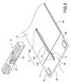
- FIG. 1shows an exploded view of the multiple-band antenna module of the present invention
- FIG. 2shows another exploded view of the multiple-band antenna module of the present invention
- FIG. 3shows yet another exploded view of the multiple-band antenna module of the present invention
- FIG. 4shows a perspective view of the multiple-band antenna module of the present invention
- FIG. 5shows a schematic view of the multiple-band antenna module of the present invention
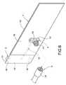
- FIG. 6shows a schematic view of the multiple-band antenna module of the present invention
- FIG. 7shows a cross-sectional view of the multiple-band antenna module of the present invention.
- FIG. 8 ashows a frequency response curve diagram of the present invention
- FIG. 8 bshows another frequency response curve diagram of the present invention
- FIG. 8 cshows a chart representing the frequency response of the present invention.
- FIG. 9shows a peak gain parameter summary of the long term evolution antenna of the present invention.
- the multiple-band antenna module of the present inventionmainly includes a substrate 1 and a carrier 2 .
- the substrate 1has a first surface 11 and a second surface 12 .
- the first surface 11has a first grounding metal surface 13 and a first micro-strip line 14 .
- the first micro-strip line 14has a front section 141 and a rear section 142 .
- the front section 141has a through hole 143 .
- the front section 141 of the first micro-strip line 14extends into the first grounding metal surface 13 .
- An interval 15is formed between the front section 141 and the first grounding metal surface 13 .
- the first grounding metal surface 13has a second micro-strip line 16 connected thereto.
- the second micro-strip line 16is parallel to the rear section 142 of the first micro-strip line 14 .
- a space 17is formed between the rear section 142 of the first micro-strip line 14 and the second micro-strip line 16 .
- the space 17 between the rear section 142 of the first micro-strip line 14 and the second micro-strip line 16is used to adjust the capacitance therebetween and thus forms a high frequency resonance point on the first grounding metal surface 13 for increasing the bandwidth.
- the first surface 11has two fixing points 18 which are used to connect with the first radiative metal portion 21 and the second radiative metal portion 22 of the carrier 2 .
- the second surface 12has a second grounding metal portion 19 for electrically connecting with a grounding portion of a connector of a coaxial cable (not shown).
- the carrier 2is of rectangular cuboid shape and is made of ceramic material with high dielectric constant.
- the carrier 2has a first radiative metal portion 21 , a second radiative metal portion 22 and a third radiative metal portion 23 .
- the first radiative metal portion 21 , the second radiative metal portion 22 and the third radiative metal portion 23each has different rectangular or stripe patterns. And the rectangular or stripe patterns are arranged on at least one surface of the carrier 2 .
- the antennacan be downsized.
- the second radiative metal portion 22is electrically connected to the first radiative metal portion 21 .
- the third radiative metal portion 23is not electrically connected to the first radiative metal portion 21 and the second radiative metal portion 22 .
- the carrier 2is electrically connected to the substrate 1 .
- the first radiative metal portion 21 and the second radiative metal portion 22are electrically connected to the two fixing points 18 on the first surface 11 of the substrate 1 .
- the carrier 2can be fixed on the first surface 11 of the substrate 1 .
- the first micro-strip line 14is electrically connected to the joint of the first radiative metal portion 21 and the second radiative metal portion 22
- the third radiative metal portion 23is electrically connected to the second micro-strip line 16 .
- FIG. 4 and FIG. 5show, after the first radiative metal portion 21 and the second radiative metal portion 22 are electrically connected to the first micro-strip line 14 , the first radiative metal portion 21 forms as a first antenna.
- the second radiative metal portion 22forms as a second antenna.
- the third radiative metal portion 23 and the second micro-strip line 16cooperatively form as a third antenna of the multiple-band antenna module.
- the signal source 3inputs through the first micro-band line 14 , and via the first radiative metal portion 21 and the second radiative metal portion 22 which form a structure including high and low frequency resonance branches.
- the width of the space 17 between the first radiative metal portion 21 and the second radiative metal portion 22can be adjusted to fine tune the coupling capacitance, thus providing a high frequency resonance point by the first grounding metal surface 13 , so as to increase the bandwidth.
- FIG. 6 and FIG. 7show a connector 4 having a shell 42 and a signal feeding probe 41 arranged inside the shell 42 .
- the signal feeding probe 41passes through the through hole 143 of the first micro-strip line 14 and electrically connects to the first micro-strip line 14 .
- the shell 42 of the connector 4is electrically connected to the second grounding metal surface 19 .
- a connector 51 of the coaxial cable 5can be connected to the connector 43 of the shell 42 .
- the first radiative metal portion 21 and the second radiative metal portion 22 and the third radiative metal portion 23can respectively used to receive signals of different frequency bands. The multiple-band antenna module is thus obtained.
- FIGS. 8 a to 8 cshow, when the multiple-band antenna module of this invention is operating at 700 MHZ, the return loss is ⁇ 3.98, the standing wave ratio is 4.20.
- the return lossis ⁇ 11.66
- the standing wave ratiois 1.73.
- the multiple-band antenna module of this inventionWhen the multiple-band antenna module of this invention is operating at 960 MHZ, the return loss is ⁇ 5.57, the standing wave ratio is 3.02.
- the return lossis ⁇ 10.39
- the standing wave ratiois 1.76.
- the return lossis ⁇ 6.38, the standing wave ratio is 2.88.
- FIG. 9shows a peak gain parameter summary of the long term evolution (LTE) antenna of the present invention.
- This inventionprovides a compact-sized surface mount device antenna module for the long term evolution antenna technology and the fourth generation communication system.
- the antenna modulecovers the bands includes 700 ⁇ 960 MHZ and 171 ⁇ 2170 MHZ, which can be applied for long term evolution antenna, global system for mobile communications (GSM), digital communications system (DCS), personal communication system (PCS), wideband code division multiple access (WCDMA).
- GSMglobal system for mobile communications
- DCSdigital communications system
- PCSpersonal communication system
- WCDMAwideband code division multiple access
Landscapes
- Engineering & Computer Science (AREA)
- Computer Networks & Wireless Communication (AREA)
- Waveguide Aerials (AREA)
- Details Of Aerials (AREA)
- Support Of Aerials (AREA)
Abstract
Description
Claims (7)
Applications Claiming Priority (3)
| Application Number | Priority Date | Filing Date | Title |
|---|---|---|---|
| TW100101869A | 2011-01-18 | ||
| TW100101869ATWI463738B (en) | 2011-01-18 | 2011-01-18 | Surface-mount multi-frequency antenna module |
| TW100101869 | 2011-01-18 |
Publications (2)
| Publication Number | Publication Date |
|---|---|
| US20120182186A1 US20120182186A1 (en) | 2012-07-19 |
| US8779988B2true US8779988B2 (en) | 2014-07-15 |
Family
ID=46490374
Family Applications (1)
| Application Number | Title | Priority Date | Filing Date |
|---|---|---|---|
| US13/351,211Active2032-08-22US8779988B2 (en) | 2011-01-18 | 2012-01-16 | Surface mount device multiple-band antenna module |
Country Status (2)
| Country | Link |
|---|---|
| US (1) | US8779988B2 (en) |
| TW (1) | TWI463738B (en) |
Cited By (9)
| Publication number | Priority date | Publication date | Assignee | Title |
|---|---|---|---|---|
| US20140253406A1 (en)* | 2013-03-11 | 2014-09-11 | Futurewei Technologies, Inc. | Segmented Antenna |
| CN104319469B (en)* | 2014-10-16 | 2017-02-15 | 云南云天化股份有限公司 | Preparation method for micro-strip ceramic antenna |
| EP3154124A1 (en)* | 2015-10-06 | 2017-04-12 | Taoglas Limited | Ten-frequency band antenna |
| EP3154125A1 (en)* | 2015-10-06 | 2017-04-12 | Taoglas Limited | Eight-frequency band antenna |
| CN106602241A (en)* | 2015-10-20 | 2017-04-26 | 锐锋股份有限公司 | Eight-frequency-band antenna |
| US20170149136A1 (en)* | 2015-11-20 | 2017-05-25 | Taoglas Limited | Eight-frequency band antenna |
| US20170149138A1 (en)* | 2015-11-20 | 2017-05-25 | Taoglas Limited | Ten-frequency band antenna |
| US20180233814A1 (en)* | 2012-10-08 | 2018-08-16 | Taoglas Group Holdings Limited | Low-cost ultra-wideband lte antenna |
| US10763578B2 (en) | 2018-07-16 | 2020-09-01 | Laird Connectivity, Inc. | Dual band multiple-input multiple-output antennas |
Families Citing this family (7)
| Publication number | Priority date | Publication date | Assignee | Title |
|---|---|---|---|---|
| USD673535S1 (en)* | 2012-06-04 | 2013-01-01 | Cheng Uei Precision Industry Co., Ltd. | Multi-band antenna |
| WO2014058926A1 (en)* | 2012-10-08 | 2014-04-17 | Zuniga Eleazar | Low cost ultra-wideband lte antenna |
| USD686599S1 (en)* | 2012-12-11 | 2013-07-23 | World Products, Llc | Multi-dimensional antenna |
| CN110676574B (en) | 2014-02-12 | 2021-01-29 | 华为终端有限公司 | Antenna and mobile terminal |
| CN106450741B (en)* | 2016-12-09 | 2023-05-05 | 广东工业大学 | Multi-frequency LTE antenna adopting novel impedance matching structure |
| TWI816140B (en)* | 2020-07-16 | 2023-09-21 | 群邁通訊股份有限公司 | Signal feeding element, antenna module, and electronc device |
| NL2033403B1 (en)* | 2022-10-27 | 2024-05-15 | The Antenna Company International N V | Antenna module which is mountable on a surface of a printed circuit board, set of two antenna modules comprising the antenna module and an auxiliary antenna module, printed circuit board on which the antenna module is mounted |
Citations (8)
| Publication number | Priority date | Publication date | Assignee | Title |
|---|---|---|---|---|
| US6323811B1 (en)* | 1999-09-30 | 2001-11-27 | Murata Manufacturing Co., Ltd. | Surface-mount antenna and communication device with surface-mount antenna |
| CN1485950A (en) | 2002-08-23 | 2004-03-31 | 株式会社村田制作所 | Antenna unit and communication device including same |
| CN1518783A (en) | 2002-07-05 | 2004-08-04 | ̫���յ���ʽ���� | Dielectric antenna, antenna mounting board, and mobile communication device |
| US20070236394A1 (en)* | 2006-04-10 | 2007-10-11 | Hitachi Metals, Ltd. | Antenna device and wireless communication apparatus using same |
| US20080238803A1 (en)* | 2007-03-30 | 2008-10-02 | Yang Tsai-Yi | Extremely miniaturized fm frequency band antenna |
| CN101308950A (en) | 2007-05-18 | 2008-11-19 | 英资莱尔德无线通信技术(北京)有限公司 | Antenna device |
| US20110043432A1 (en)* | 2007-11-26 | 2011-02-24 | Ineichen Alois | Microwave antenna for wireless networking of devices in automation technology |
| CN201994418U (en) | 2011-01-27 | 2011-09-28 | 太盟光电科技股份有限公司 | Surface mount multi-frequency antenna module |
Family Cites Families (3)
| Publication number | Priority date | Publication date | Assignee | Title |
|---|---|---|---|---|
| JP3752474B2 (en)* | 2002-06-19 | 2006-03-08 | 京セラ株式会社 | Surface mount antenna and antenna device |
| TWI245451B (en)* | 2005-02-18 | 2005-12-11 | Advanced Connectek Inc | A planar inverted-f antenna |
| TWI351786B (en)* | 2007-11-22 | 2011-11-01 | Arcadyan Technology Corp | Dual band antenna |
- 2011
- 2011-01-18TWTW100101869Apatent/TWI463738B/enactive
- 2012
- 2012-01-16USUS13/351,211patent/US8779988B2/enactiveActive
Patent Citations (9)
| Publication number | Priority date | Publication date | Assignee | Title |
|---|---|---|---|---|
| US6323811B1 (en)* | 1999-09-30 | 2001-11-27 | Murata Manufacturing Co., Ltd. | Surface-mount antenna and communication device with surface-mount antenna |
| CN1518783A (en) | 2002-07-05 | 2004-08-04 | ̫���յ���ʽ���� | Dielectric antenna, antenna mounting board, and mobile communication device |
| US20040246180A1 (en)* | 2002-07-05 | 2004-12-09 | Hironori Okado | Dielectric antenna, antenna-mounted substrate, and mobile communication machine having them therein |
| CN1485950A (en) | 2002-08-23 | 2004-03-31 | 株式会社村田制作所 | Antenna unit and communication device including same |
| US20070236394A1 (en)* | 2006-04-10 | 2007-10-11 | Hitachi Metals, Ltd. | Antenna device and wireless communication apparatus using same |
| US20080238803A1 (en)* | 2007-03-30 | 2008-10-02 | Yang Tsai-Yi | Extremely miniaturized fm frequency band antenna |
| CN101308950A (en) | 2007-05-18 | 2008-11-19 | 英资莱尔德无线通信技术(北京)有限公司 | Antenna device |
| US20110043432A1 (en)* | 2007-11-26 | 2011-02-24 | Ineichen Alois | Microwave antenna for wireless networking of devices in automation technology |
| CN201994418U (en) | 2011-01-27 | 2011-09-28 | 太盟光电科技股份有限公司 | Surface mount multi-frequency antenna module |
Non-Patent Citations (1)
| Title |
|---|
| China Official Action issued on Sep. 9, 2013. |
Cited By (27)
| Publication number | Priority date | Publication date | Assignee | Title |
|---|---|---|---|---|
| US20180233814A1 (en)* | 2012-10-08 | 2018-08-16 | Taoglas Group Holdings Limited | Low-cost ultra-wideband lte antenna |
| US11705626B2 (en) | 2012-10-08 | 2023-07-18 | Taogals Group Holdings Limited | Ultra-wideband antenna |
| US11088442B2 (en) | 2012-10-08 | 2021-08-10 | Taoglas Group Holdings Limited | Ultra-wideband LTE antenna system |
| US11081784B2 (en) | 2012-10-08 | 2021-08-03 | Taoglas Group Holdings Limited | Ultra-wideband LTE antenna system |
| US10283854B2 (en) | 2012-10-08 | 2019-05-07 | Taoglas Group Holdings Limited | Low-cost ultra wideband LTE antenna |
| US10135129B2 (en)* | 2012-10-08 | 2018-11-20 | Taoglas Group Holding Limited | Low-cost ultra wideband LTE antenna |
| US20140253406A1 (en)* | 2013-03-11 | 2014-09-11 | Futurewei Technologies, Inc. | Segmented Antenna |
| US10170837B2 (en)* | 2013-03-11 | 2019-01-01 | Futurewei Technologies, Inc. | Segmented antenna |
| CN104319469B (en)* | 2014-10-16 | 2017-02-15 | 云南云天化股份有限公司 | Preparation method for micro-strip ceramic antenna |
| EP3444896A1 (en)* | 2015-10-06 | 2019-02-20 | Taoglas Limited | Ten-frequency band antenna |
| EP3154124A1 (en)* | 2015-10-06 | 2017-04-12 | Taoglas Limited | Ten-frequency band antenna |
| EP3154125A1 (en)* | 2015-10-06 | 2017-04-12 | Taoglas Limited | Eight-frequency band antenna |
| CN106602241B (en)* | 2015-10-20 | 2020-03-31 | 锐锋股份有限公司 | Eight-frequency-band antenna |
| CN106602241A (en)* | 2015-10-20 | 2017-04-26 | 锐锋股份有限公司 | Eight-frequency-band antenna |
| US10483644B2 (en)* | 2015-11-20 | 2019-11-19 | Taoglas Group Holdings Limited | Eight-frequency band antenna |
| US10601135B2 (en)* | 2015-11-20 | 2020-03-24 | Taoglas Group Holdings Limited | Ten-frequency band antenna |
| US20170358861A1 (en)* | 2015-11-20 | 2017-12-14 | Taoglas Group Holdings Limited | Ten-frequency band antenna |
| US20170149136A1 (en)* | 2015-11-20 | 2017-05-25 | Taoglas Limited | Eight-frequency band antenna |
| US20170149138A1 (en)* | 2015-11-20 | 2017-05-25 | Taoglas Limited | Ten-frequency band antenna |
| US11264718B2 (en)* | 2015-11-20 | 2022-03-01 | Taoglas Group Holdings Limited | Eight-frequency band antenna |
| USRE49000E1 (en)* | 2015-11-20 | 2022-03-29 | Taoglas Group Holdings Limited | Ten-frequency band antenna |
| US11342674B2 (en) | 2015-11-20 | 2022-05-24 | Taoglas Group Holdings Limited | Ten-frequency band antenna |
| US20220224009A1 (en)* | 2015-11-20 | 2022-07-14 | Taoglas Group Holdings Limited | Multi-frequency band antenna |
| US11641060B2 (en) | 2015-11-20 | 2023-05-02 | Taoglas Group Holdings Limited | Multi-frequency band antenna |
| US9755310B2 (en)* | 2015-11-20 | 2017-09-05 | Taoglas Limited | Ten-frequency band antenna |
| US12034231B2 (en) | 2015-11-20 | 2024-07-09 | Taoglas Group Holdings Limited | Multi-frequency band antenna |
| US10763578B2 (en) | 2018-07-16 | 2020-09-01 | Laird Connectivity, Inc. | Dual band multiple-input multiple-output antennas |
Also Published As
| Publication number | Publication date |
|---|---|
| TWI463738B (en) | 2014-12-01 |
| US20120182186A1 (en) | 2012-07-19 |
| TW201232924A (en) | 2012-08-01 |
Similar Documents
| Publication | Publication Date | Title |
|---|---|---|
| US8779988B2 (en) | Surface mount device multiple-band antenna module | |
| US11063343B2 (en) | Mobile device and antenna structure | |
| CN106575816B (en) | Ultra-thin launch system for electronic devices | |
| TWI425713B (en) | Three-band antenna device with resonance generation | |
| US6894647B2 (en) | Inverted-F antenna | |
| US7642966B2 (en) | Carrier and device | |
| US20150364820A1 (en) | Multiband antenna apparatus and methods | |
| US20110102272A1 (en) | Mobile Communication Device and Antenna Thereof | |
| US20130113671A1 (en) | Slot antenna | |
| US20100309087A1 (en) | Chip antenna device | |
| JP2011155630A (en) | Antenna module | |
| US20210167521A1 (en) | Antenna structure | |
| US11329382B1 (en) | Antenna structure | |
| CN103943942B (en) | Antenna and portable device with the antenna | |
| CN102623801A (en) | Surface-mounted multi-frequency antenna module | |
| US9793609B2 (en) | Surface-mount multi-band antenna | |
| US8299969B2 (en) | Multiband antenna | |
| CN100399625C (en) | Concealed antenna | |
| US11996630B2 (en) | Antenna structure | |
| US9431710B2 (en) | Printed wide band monopole antenna module | |
| US20080094293A1 (en) | Broadband antenna | |
| US20080129611A1 (en) | Antenna module and electronic device using the same | |
| CN1964132B (en) | Hidden Multi-Band Antennas for Portable Devices | |
| CN108459660B (en) | electronic device | |
| CN106033834A (en) | antenna structure |
Legal Events
| Date | Code | Title | Description |
|---|---|---|---|
| AS | Assignment | Owner name:TAOGLAS GROUP HOLDINGS LIMITED., IRELAND Free format text:ASSIGNMENT OF ASSIGNORS INTEREST;ASSIGNORS:YANG, TSAI-YI;WU, CHIA-TSUNG;REEL/FRAME:027538/0795 Effective date:20110224 Owner name:CIROCOMM TECHNOLOGY CORP., TAIWAN Free format text:ASSIGNMENT OF ASSIGNORS INTEREST;ASSIGNORS:YANG, TSAI-YI;WU, CHIA-TSUNG;REEL/FRAME:027538/0795 Effective date:20110224 | |
| STCF | Information on status: patent grant | Free format text:PATENTED CASE | |
| MAFP | Maintenance fee payment | Free format text:PAYMENT OF MAINTENANCE FEE, 4TH YR, SMALL ENTITY (ORIGINAL EVENT CODE: M2551) Year of fee payment:4 | |
| FEPP | Fee payment procedure | Free format text:ENTITY STATUS SET TO UNDISCOUNTED (ORIGINAL EVENT CODE: BIG.); ENTITY STATUS OF PATENT OWNER: LARGE ENTITY Free format text:PETITION RELATED TO MAINTENANCE FEES GRANTED (ORIGINAL EVENT CODE: PTGR); ENTITY STATUS OF PATENT OWNER: LARGE ENTITY | |
| MAFP | Maintenance fee payment | Free format text:PAYMENT OF MAINTENANCE FEE UNDER 1.28(C) (ORIGINAL EVENT CODE: M1559); ENTITY STATUS OF PATENT OWNER: LARGE ENTITY | |
| FEPP | Fee payment procedure | Free format text:ENTITY STATUS SET TO SMALL (ORIGINAL EVENT CODE: SMAL); ENTITY STATUS OF PATENT OWNER: SMALL ENTITY | |
| MAFP | Maintenance fee payment | Free format text:PAYMENT OF MAINTENANCE FEE, 8TH YR, SMALL ENTITY (ORIGINAL EVENT CODE: M2552); ENTITY STATUS OF PATENT OWNER: SMALL ENTITY Year of fee payment:8 | |
| AS | Assignment | Owner name:BAIN CAPITAL CREDIT, LP, MASSACHUSETTS Free format text:SECURITY INTEREST;ASSIGNOR:TAOGLAS GROUP HOLDINGS LIMITED;REEL/FRAME:066818/0035 Effective date:20230306 |