US8779322B2 - Method and apparatus for processing metal bearing gases - Google Patents
Method and apparatus for processing metal bearing gasesDownload PDFInfo
- Publication number
- US8779322B2 US8779322B2US13/336,616US201113336616AUS8779322B2US 8779322 B2US8779322 B2US 8779322B2US 201113336616 AUS201113336616 AUS 201113336616AUS 8779322 B2US8779322 B2US 8779322B2
- Authority
- US
- United States
- Prior art keywords
- plasma
- plasma chamber
- metal
- chamber
- gas
- Prior art date
- Legal status (The legal status is an assumption and is not a legal conclusion. Google has not performed a legal analysis and makes no representation as to the accuracy of the status listed.)
- Expired - Fee Related, expires
Links
Images


Classifications
- H—ELECTRICITY
- H01—ELECTRIC ELEMENTS
- H01J—ELECTRIC DISCHARGE TUBES OR DISCHARGE LAMPS
- H01J37/00—Discharge tubes with provision for introducing objects or material to be exposed to the discharge, e.g. for the purpose of examination or processing thereof
- H01J37/32—Gas-filled discharge tubes
- H01J37/32009—Arrangements for generation of plasma specially adapted for examination or treatment of objects, e.g. plasma sources
- H01J37/32082—Radio frequency generated discharge
- H01J37/32174—Circuits specially adapted for controlling the RF discharge
- H—ELECTRICITY
- H01—ELECTRIC ELEMENTS
- H01J—ELECTRIC DISCHARGE TUBES OR DISCHARGE LAMPS
- H01J37/00—Discharge tubes with provision for introducing objects or material to be exposed to the discharge, e.g. for the purpose of examination or processing thereof
- H01J37/32—Gas-filled discharge tubes
- H01J37/32009—Arrangements for generation of plasma specially adapted for examination or treatment of objects, e.g. plasma sources
- H01J37/32082—Radio frequency generated discharge
- H01J37/321—Radio frequency generated discharge the radio frequency energy being inductively coupled to the plasma
Definitions
- This inventionrelates generally to the field of generating activated gas containing ions, free radicals, atoms and molecules and to apparatus for and methods of processing materials with activated gas.
- Plasma dischargescan be used to excite gases to produce activated gases containing ions, free radicals, atoms and molecules.
- Activated gasesare used for numerous industrial and scientific applications including processing solid materials such as semiconductor wafers, powders, and other gases.
- the parameters of the plasma and the conditions of the exposure of the plasma to the material being processedvary widely depending on the application.
- some applicationsrequire the use of ions with low kinetic energy (i.e. a few electron volts) because the material being processed is sensitive to damage.
- Other applicationssuch as anisotropic etching or planarized dielectric deposition, require the use of ions with high kinetic energy.
- Still other applications, such as reactive ion beam etching,require precise control of the ion energy.
- Some applicationsrequire direct exposure of the material being processed to a high density plasma.
- One such applicationis generating ion-activated chemical reactions.
- Other such applicationsinclude etching of and depositing material into high aspect ratio structures.
- Other applicationsrequire shielding the material being processed from the plasma because the material is sensitive to damage caused by ions or because the process has high selectivity requirements.
- Plasmascan be generated in various ways including DC discharge, radio frequency (RF) discharge, and microwave discharge.
- DC dischargesare achieved by applying a potential between two electrodes in a gas.
- RF dischargesare achieved either by electrostatically or inductively coupling energy from a power supply into a plasma.
- Parallel platesare typically used for electrostatically coupling energy into a plasma.
- Induction coilsare typically used for inducing current into the plasma.
- Microwave dischargesare achieved by directly coupling microwave energy through a microwave-passing window into a discharge chamber containing a gas. Microwave discharges are advantageous because they can be used to support a wide range of discharge conditions, including highly ionized electron cyclotron resonant (ECR) plasmas.
- ECRelectron cyclotron resonant
- RF discharges and DC dischargesinherently produce high energy ions and, therefore, are often used to generate plasmas for applications where the material being processed is in direct contact with the plasma.
- Microwave dischargesproduce dense, low ion energy plasmas and, therefore, are often used to produce streams of activated gas for “downstream” processing. Microwave discharges are also useful for applications where it is desirable to generate ions at low energy and then accelerate the ions to the process surface with an applied potential.
- microwave and inductively coupled plasma sourcesrequire expensive and complex power delivery systems. These plasma sources require precision RF or microwave power generators and complex matching networks to match the impedance of the generator to the plasma source. In addition, precision instrumentation is usually required to ascertain and control the actual power reaching the plasma.
- RF inductively coupled plasmasare particularly useful for generating large area plasmas for such applications as semiconductor wafer processing.
- prior art RF inductively coupled plasmasare not purely inductive because the drive currents are only weakly coupled to the plasma. Consequently, RF inductively coupled plasmas are inefficient and require the use of high voltages on the drive coils.
- the high voltagesproduce high electrostatic fields that cause high energy ion bombardment of reactor surfaces. The ion bombardment deteriorates the reactor and can contaminate the process chamber and the material being processed. The ion bombardment can also cause damage to the material being processed.
- Faraday shieldshave been used in inductively coupled plasma sources to contain the high electrostatic fields.
- large eddy currentsform in the shields resulting in substantial power dissipation.
- the cost, complexity, and reduced power efficiencymake the use of Faraday shields unattractive.
- the inventionin one embodiment, features an apparatus for processing metal bearing gases.
- the apparatusincludes an inlet and a plasma chamber for containing a metal bearing gas.
- the apparatusalso includes a transformer having a primary winding and a magnetic core surrounding a portion of the plasma chamber.
- the apparatusalso includes a solid state switching power supply comprising one or more switching semiconductor devices coupled to a voltage supply and having an output coupled to the primary winding, the switching power supply driving current in the primary winding, the current inducing a potential inside the chamber that directly forms a toroidal plasma which completes a secondary circuit of the transformer and which reacts with the metal bearing gas.
- At least a second gas(e.g., one or more of H 2 , H 2 O and O 2 ) is provided to the plasma chamber via the inlet. Reactions of the metal-containing gases with one or more second gases can convert the metal-containing gases to a solid form such as metals, metal oxides, or metal nitrides. Alternatively, the reactions may convert the metal-containing gases to different gaseous compounds that can be utilized or treated subsequently.
- the apparatuscan include a device for collecting a metallic material, a metal oxide material or a metal nitride material produced by the interaction of the plasma with the metal bearing gas. The device can be, for example, a filter, a particle trap, a cyclone trap and an electrostatic trap.
- the deviceis located external to the plasma chamber.
- a portion of the plasma chambere.g., a replaceable component of the plasma chamber collects a metallic material, a metal oxide material or a metal nitride material produced by the interaction of the plasma with the metal bearing gas.
- the metal bearing gascan include fluorine.
- the metal bearing gascan be, for example, WF 6 , UF 6 , SF 4 or metal organics.
- the plasma chambercan include at least one of a metallic material, coated metallic material or dielectric material. In some embodiments, the plasma chamber includes a ceramic or quartz material.
- the inventionin another aspect, features an apparatus for processing metal bearing gases.
- the apparatusincludes an inlet and a plasma chamber for containing a metal bearing gas.
- the plasma chamberincludes an electrically conductive material and at least one dielectric region that forms an electrical discontinuity in the plasma chamber.
- the apparatusalso includes a transformer having a primary winding and a magnetic core surrounding a portion of the plasma chamber.
- the apparatusalso includes a power supply having an output electrically connected to the primary winding, the power supply driving current in the primary winding, the current inducing a potential inside the chamber that forms a toroidal plasma which completes a secondary circuit of the transformer and which reacts with the metal bearing gas.
- the inventionin another aspect, relates to a method for processing metal bearing gases.
- the methodinvolves receiving a metal bearing gas in a plasma chamber at pressure via an inlet.
- the methodalso involves forming a toroidal plasma inside the plasma chamber, by passing current, generated by a solid state switching power supply comprising one or more switching semiconductor devices, through a primary winding of a transformer having a magnetic core surrounding a portion of the plasma chamber, the toroidal plasma reacting with the metal bearing gas to produce at least one of a metallic material, a metal oxide material or a metal nitride material.
- the methodalso can involve providing at least a second gas to the plasma chamber.
- the methodalso can involve producing a metal oxide material or a metal nitride material by the interaction of the plasma, the metal bearing gas and the second gas.
- the methodalso can involve outputting the at least one of a metallic material, a metal oxide material or a metal nitride material from the plasma chamber.
- the methodalso can involve collecting the at least one of a metallic material, a metal oxide material or a metal nitride material produced by the interaction of the plasma with the metal bearing gas.
- the methodalso can involve filtering the at least one of a metallic material, a metal oxide material or a metal nitride material from an output of the plasma chamber.
- the inventionin another aspect, features an apparatus for processing metal bearing gases.
- the apparatusincludes a means for receiving a metal bearing gas in a plasma chamber at pressure via an inlet.
- the apparatusalso includes a means for forming a toroidal plasma inside the plasma chamber, by passing current, generated by a solid state switching power supply comprising one or more switching semiconductor devices, through a primary winding of a transformer having a magnetic core surrounding a portion of the plasma chamber, the toroidal plasma reacting with the metal bearing gas to produce at least one of a metallic material, a metal oxide material or a metal nitride material.
- the inventionin another aspect, features a plasma source that forms a toroidal plasma that reacts with a metal bearing gas or a silicon bearing gas.
- the plasma sourcecan be a low power plasma source and/or operate at low voltage levels.
- the inventionin another aspect, features a plasma source that includes more than one high permeability magnetic core that surround the plasma chamber.
- separate switching power suppliesare coupled to the primary winding of each of the high permeability magnetic cores.
- a single power supplyis coupled to the primary winding of each of the high permeability magnetic cores.
- the plasma chamberincludes imbedded cooling channels for passing a fluid that controls the temperature of the plasma chamber.
- the plasma chamberis formed of quartz and is thermally bonded to a fluid cooled supporting structure.
- the plasma chamberis formed of anodized aluminum and is thermally bonded to a fluid cooled supporting structure.
- the plasma chamberis formed of metal.
- Metal plasma chambersinclude multiple dielectric regions that prevent induced current flow from forming in the plasma chamber.
- the metal plasma chamberis segmented with multiple dielectric gaps to reduce the potential difference between the plasma and the metal plasma chamber, thereby distributing the plasma loop voltage across multiple dielectric gaps.
- the segmented plasma chamberfacilitates operating the plasma source at relatively high loop voltages, while reducing or eliminating the plasma channel surface erosion.
- circuit elementsare used to control the voltage distribution across the metal plasma chamber.
- the power supply of the high power sourceincludes a voltage regulator circuit that provides a stable DC bus voltage that allows the user to precisely control the total power supplied to the plasma.
- the high power toroidal plasma source of the present inventionincludes an apparatus for reliably igniting the plasma.
- the inventionin another aspect, features a high power toroidal plasma source.
- the high power toroidal plasma sourcein one embodiment of the present invention, has numerous advantages.
- the high power plasma sourcegenerates a relatively high power plasma with higher operating voltages that has increased dissociation rates and that allow a wider operating pressure range.
- the high power plasma sourcehas precise process control.
- the high power plasma sourcehas relatively low plasma chamber surface erosion.
- the present inventionfeatures apparatus for dissociating or activating gases that includes a plasma chamber comprising a gas.
- the plasma chambermay comprise a portion of an outer surface of a process chamber.
- the plasma chambercomprises a dielectric material.
- the dielectric materialmay be quartz.
- the dielectric materialmay be thermally bonded to a supporting structure.
- the supporting structuremay include cooling channels that transport cooling fluid.
- the plasma chamberis formed of an electrically conductive material and at least one dielectric region that forms an electrical discontinuity in the conductive material.
- the electrically conductive materialmay be aluminum and the aluminum may be anodized.
- the electrically conductive materialmay be segmented with at least two dielectric gaps. The dielectric gaps reduce the potential difference between the plasma and the metal plasma chamber, thereby distributing the plasma loop voltage across the at least two dielectric gaps.
- a voltage divider circuitmay be electrically coupled across the at least two dielectric gaps to distribute the plasma loop voltage across the at least two dielectric gaps.
- the apparatusincludes a first and second transformer.
- the first transformerhas a first magnetic core surrounding a first portion of the plasma chamber and has a first primary winding.
- the second transformerhas a second magnetic core that surrounds a second portion of the plasma chamber and has a second primary winding.
- the apparatusalso includes first and second solid state AC switching power supply.
- the first solid state AC switching power supplyincludes one or more switching semiconductor devices that is coupled to a first voltage supply and has a first output that is coupled to the first primary winding.
- the second solid state AC switching power supplyincludes one or more switching semiconductor devices that is coupled to a second voltage supply and has a second output that is coupled to the second primary winding.
- the voltage suppliesmay include a voltage regulator circuit.
- the one or more switching semiconductor devicesmay be switching transistors. In one embodiment, the output of the one or more switching semiconductor devices is directly coupled to the primary winding.
- the solid state AC switching power suppliesmay be substantially identical. Also, the solid state AC switching power supplies may comprise a single power supply unit.
- the first solid state AC switching power supplydrives a first AC current in the first primary winding.
- the second solid state AC switching power supplydrives a second AC current in the second primary winding.
- the first AC current and the second AC currentinduce a combined AC potential inside the plasma chamber that directly forms a toroidal plasma that completes a secondary circuit of the transformer and that dissociates the gas.
- the apparatusincludes an apparatus to assist in igniting the plasma.
- an electrodeis positioned in the plasma chamber that generates free charges that assist the ignition of the plasma in the plasma chamber.
- an electrodemay be capacitively coupled externally from the dielectric plasma chamber to assist in ignition in the plasma chamber.
- the apparatusincludes a secondary winding that resonates with the primary winding and raises the voltage in the plasma chamber to assist ignition of the plasma in the plasma chamber.
- an ultraviolet light sourceis optically coupled to the plasma chamber. The ultraviolet light source generates free changes that assist the ignition of the plasma in the plasma chamber.
- the present inventionalso features a method for dissociating or activating gases.
- the methodincludes confining a gas in a plasma chamber at a pressure.
- a first and a second currentare generated with a first and a second solid state AC switching power supply.
- the first and the second currentinduce a combined AC potential inside the plasma chamber by passing the first current though a first primary winding having a first magnetic core surrounding a first portion of the plasma chamber, and by passing the second current though a second primary winding having a second magnetic core surrounding a second portion of the plasma chamber.
- the combined induced AC potentialdirectly forms a toroidal plasma that completes a secondary circuit of the transformer and dissociates the gas.
- the methodmay be used for cleaning process chambers.
- the methodmay include regulating the current generated with the first and the second solid state AC switching power supply.
- the methodmay also include providing an initial ionization event in the plasma chamber.
- the methodmay include measuring electrical parameters of the primary and secondary and adjusting a magnitude of the current generated by the first and the second solid state AC switching power supply in response to the measured electrical parameters.
- FIG. 1is a schematic representation of a toroidal low-field plasma source for producing activated gases that embodies the invention.
- FIG. 2illustrates a plot of etch rate of thermal silicon dioxide as a function of NF3 feed gas flow rate, using the toroidal low-field plasma source that embodies the invention.
- FIG. 3is a schematic cross-sectional representation of a metallic plasma chamber that may be used with the toroidal low-field plasma source described in connection with FIG. 1 .
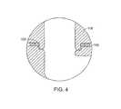
- FIG. 4is a schematic representation of a dielectric spacer suitable for the dielectric regions illustrated in FIG. 3 that prevent induced current flow from forming in the plasma chamber.
- FIG. 5is a schematic representation of a toroidal low-field ion beam source that embodies the invention and that is configured for high intensity ion beam processing.
- FIG. 6is a schematic block diagram of a solid state switching power supply that includes the one or more switching semiconductor devices of FIG. 1 .
- FIGS. 7 a and billustrate boost voltage regulator circuits that facilitate stable operation of the toroidal plasma source of an illustrative embodiment of the present invention.
- FIGS. 8 a - cillustrate apparatus for igniting a plasma in the toroidal plasma source of an illustrative embodiment of the present invention.
- FIG. 9illustrates a schematic cross-section of a high power toroidal low-field plasma source for producing activated gases according to an illustrative embodiment of the present invention.
- FIG. 10illustrates a low-field toroidal plasma source according to an illustrative embodiment of the present invention that includes a segmented plasma chamber that has relatively low surface erosion.
- FIG. 11 aillustrates a side view of one embodiment of the low-field toroidal plasma source according to an illustrative embodiment of the present invention that includes a quartz plasma chamber and a metal supporting structure.
- FIG. 11 billustrates a center cross section of the low-field toroidal plasma source according to an illustrative embodiment of the present invention that includes a quartz plasma chamber and a metal supporting structure.
- FIG. 11 cillustrates an off center cross section of the low-field toroidal plasma source according to an illustrative embodiment of the present invention that includes a quartz plasma chamber and a metal supporting structure.
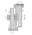
- FIG. 12is a partial schematic view of an apparatus for processing metal bearing gases that embodies the invention.
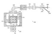
- FIG. 1is a schematic representation of a toroidal low-field plasma source 10 for producing activated gases that embodies the invention.
- the source 10includes a power transformer 12 that couples electromagnetic energy into a plasma 14 .
- the power transformer 12includes a high permeability magnetic core 16 , a primary coil 18 , and a plasma chamber 20 that contains the plasma 14 , which allows the plasma 14 to form a secondary circuit of the transformer 12 .
- the power transformer 12can include additional magnetic cores and primary coils (not shown) that form additional secondary circuits.
- One or more sides of the plasma chamber 20are exposed to a process chamber 22 to allow charged particles and activated gases generated by the plasma 14 to be in direct contact with a material to be processed (not shown).
- a sample holder 23may be positioned in the process chamber 22 to support the material to be processed.
- the material to be processedmay be biased relative to the potential of the plasma.
- the materials used in the internal surface of the plasma chamber 20 and the vacuum elements that connect the output of the plasma chamber 20 to the process chamber 22must be carefully chosen, especially if the plasma source will be used to generate chemically reactive species. Materials are selected to meet several requirements. One requirement of the materials is that the creation of contamination that results from corrosion or deterioration of the material caused by interaction of the materials with the process gases should be minimized. Another requirement of the materials is that they have minimal erosion when exposed to process gases. Another requirement of the materials is that they should minimize recombination and deactivation of the reactive gas, thus maximizing reactant delivery to the process chamber.
- Anodized aluminumhas some advantages for semiconductor processing applications.
- One advantageis that anodized aluminum can be grown directly on an underlying aluminum base through an electroplating process. The resulting film has excellent adherence properties.
- Another advantageis that anodized aluminum has a thermal conductivity that is approximately 15 times greater than the thermal conductivity of quartz. Therefore, the inside surface of plasma chambers that are formed with anodized aluminum will remain relatively cool, even with significant incident power density.
- anodized aluminumis chemically inert to many atomic species (F, O, Cl, etc.) as long as there is no or only low-energy ion bombardment present.
- Anodized aluminumis particularly advantageous for fluorine chemistries because it has a low recombination coefficient for atomic fluorine.
- anodized aluminumis a material that is commonly used and accepted for semiconductor materials processing applications.
- Quartzalso has some advantages for semiconductor processing applications. Quartz is available in extremely high purity and is commonly used and accepted in the semiconductor industry. Also, quartz is stable with numerous reactive species including O, H, N, Cl, and Br. In particular, quartz has a low surface recombination coefficient for atomic oxygen and hydrogen. Also, quartz has a low thermal coefficient of expansion and has relatively high resistance to thermal shock. In addition, quartz has a high softening and melting point and, therefore, it is relatively easy to form a process chamber from quartz.
- Fluoropolymersalso have some advantages for semiconductor processing applications. Examples of some fluoropolymers are PTFE, PFE, PFA, FEP, and TeflonTM. The recombination rate for many fluoropolymers is relatively low. Fluoropolymers also are relatively inert to most atomic species including atomic fluorine and atomic oxygen. In addition, the purity of fluoropolymers is relatively high and fluoropolymers are available in both bulk form (tube, sheet, etc.) and in thin film form.
- fluoropolymerscan be eroded by ions in the plasma. Also, the maximum operating temperature that fluoropolymers can tolerate is significantly less than the maximum temperature that quartz can tolerate. In addition, the thermal conductivity of fluoropolymers is relatively low. Therefore, in some embodiments, fluoropolymers are most useful for constructing the transport sections outside of the plasma chamber.
- a voltage supply 24which may be a line voltage supply or a bus voltage supply, is directly coupled to a switching circuit 26 containing one or more switching semiconductor devices.
- the one or more switching semiconductor devicesmay be switching transistors.
- the circuitmay be a solid state switching power supply.
- An output 28 of the switching circuit 26may be directly coupled to the primary winding 18 of the transformer 12 .
- the toroidal low field plasma source 10may include an apparatus for generating free charges that provides an initial ionization event that ignites a plasma in the plasma chamber 20 as described herein.
- a noble gassuch as argon, may also be inserted into the plasma chamber 20 to reduce the voltage required to ignite a plasma.
- Free chargescan be generated in numerous ways as described herein. For example, free charges can be generated by applying a short high voltage pulse to an electrode inside of the plasma chamber 20 . Also, free charges can be generated by applying a short high voltage pulse directly to the primary coil 18 . In another embodiment, a high electric voltage signal may be applied to an electrode, located outside of a dielectric plasma chamber 20 but capacitively coupled to the plasma volume, to generate free charges to assist ignition in the plasma chamber 20 .
- an ultraviolet light source 34is used to generate free charges that provide an initial ionization event, which ignites a plasma in the plasma chamber 20 .
- the ultraviolet (UV) light source 34is optically coupled to the plasma chamber 20 .
- the UV light source 34may be optically coupled to the plasma channel through an optically transparent window.
- the UV light source 34may either be a continuous wave (CW) light source or a pulsed light source depending on the duty cycle of the plasma source.
- the toroidal low field plasma source 10may also include a measuring circuit 36 for measuring electrical parameters of the primary winding 18 .
- Electrical parameters of the primary winding 18include the current driving the primary winding 18 , the voltage across the primary winding 18 , the bus or line voltage that is generated by the voltage supply 24 , the average power in the primary winding 18 , and the peak power in the primary winding 18 .
- the electric parameters of the primary windingmay be continuously monitored.
- the plasma source 10may also include an apparatus for measuring electrical and optical parameters of the plasma 14 itself.
- the source 10may include a current probe 38 that is positioned around the plasma chamber 20 to measure the plasma current flowing in secondary of the transformer 12 .
- the voltage on the plasma secondarycan be measured, for example, by positioning a secondary winding on the magnetic core parallel to the plasma 14 .
- the electric power applied to the plasmamay be determined from measurements of the AC line voltage and current and from known losses in the electric circuit.
- the plasma source 10may also include an optical detector 40 for measuring the optical emission from the plasma 14 .
- the electric and optical parameters of the plasma 14may be continuously monitored.
- the plasma source 10may include a power control circuit 42 that accepts data from at least one of the current probe 38 , the power detector 40 , and the switching circuit 26 and then adjusts the power in the plasma by adjusting the current in the primary winding 18 .
- a gasis bled into the plasma chamber 20 until a pressure that is substantially between 1 mtorr and 100 torr is reached. In some embodiments, a gas is bled into the chamber 20 until a pressure that is between about 0.1 mTorr and about 1,000 Torr is reached.
- the gasmay comprise a noble gas, a reactive gas or a mixture of at least one noble gas and at least one reactive gas.
- the switching circuit 26containing switching semiconductor devices that supply a current to the primary winding 18 that induces a potential inside the plasma chamber 20 .
- the magnitude of the induced potentialdepends on the magnetic field produced by the magnetic core 16 and the frequency at which the switching semiconductor devices operate according to Faraday's law of induction.
- An ionization event that forms the plasmamay be initiated in the chamber 20 .
- the ionization eventmay be the application of a voltage pulse to the primary winding or to the electrode 30 positioned in the chamber 20 as described herein.
- the ionization eventmay be exposing the inside of the plasma chamber 20 to ultraviolet radiation.
- a plasmais formed in the plasma chamber 20 that completes a secondary circuit of the transformer 12 .
- the shape of the plasma 14can vary from circular to non-circular (oval, etc.).
- the diameter of a circular plasma 14may vary from approximately 0.5 to 2.0 inches depending upon the operating conditions. Changing the diameter of the plasma 14 changes the gas flow dynamics and the plasma impedance and allows the plasma source to be optimized for different operating ranges (i.e. different power levels, pressures ranges, gases, and gas flow rates).
- the ratio of the maximum to the minimum dimensionmay vary from about 1 (i.e. a circular cross section) to 10 depending upon the particular application.
- the electric field of the plasmamay be substantially between about 1-200 V/cm. If only noble gases are present in the plasma chamber 20 , the electric fields in the plasma 14 may be as low as 1 volt/cm. If, however, electronegative gases are present in the plasma chamber 20 , then the electric fields in the plasma 14 are considerably higher. In some embodiments, operating the plasma source 10 with low electric fields in the plasma 14 is desirable because a low potential difference between the plasma 14 and the chamber 20 will substantially reduce erosion of the chamber 20 caused by energetic ions. This will substantially reduce the resulting contamination to the material being processed. Reducing erosion of the chamber 20 is not required in some embodiments.
- the power delivered to the plasmacan be accurately controlled by a feedback loop 44 that comprises the power control circuit 42 , the measuring circuit 36 for measuring electrical parameters of the primary winding 18 and the switching circuit 26 containing one or more switching semiconductor devices.
- the feedback loop 44may include the current probe 38 and optical detector 40 .
- the power control circuit 42measures the power in the plasma using the measuring circuit 36 for measuring electrical parameters of the primary winding 18 .
- the power control circuit 42compares the resulting measurement to a predetermined value representing a desired operating condition and then adjusts one or more parameters of the switching circuit 26 to control the power delivered to the plasma.
- the one or more parameters of switching circuit 26include, for example, voltage and current amplitude, frequency, pulse width, and relative phase of the drive pulses to the one or more switching semiconductor devices.
- the power control circuit 42measures the power in the plasma using the current probe 38 or the optical detector 40 .
- the power control circuit 42then compares the measurement to a predetermined value representing a desired operating condition and then adjusts one or more parameters of the switching circuit 26 to control the power delivered to the plasma.
- the plasma source 10may include protection circuits to ensure that the plasma source 10 is not damaged either through abnormal environmental conditions or through abnormal usage.
- the temperature of the plasma source 10may be monitored at numerous locations to ensure that an appropriate amount of cooling fluid is flowing and that an abnormally high amount of power is not being dissipated in the source.
- the temperature of the mounting blocks for the switching devices, the plasma chamber 20 itself, and the magnetic coremay be monitored.
- the current flowing though the FET devicesmay be monitored. If the current exceeds predetermined values the plasma source 10 may be shut down, thereby protecting the switching devices against possible damage.
- the plasma source 10is advantageous because its conversion efficiency of line power into power absorbed by the plasma is very high compared with prior art plasma sources. This is because the switching circuit 26 containing one or more switching semiconductor devices that supplies the current to the primary winding 18 is highly efficient. The conversion efficiency may be substantially greater than 90%.
- the plasma source 10is also advantageous because it does not require the use of conventional impedance matching networks or conventional RF power generators. This greatly reduces the cost and increases the reliability of the plasma source.
- the plasma source 10is advantageous because it operates with low electric fields in the plasma chamber 20 .
- Low electric fieldsare desirable because a low potential difference between the plasma and the chamber will substantially reduce energetic ion bombardment within the plasma chamber 20 .
- Reducing energetic ion bombardment in the plasma chamber 20is desirable because it minimizes the production of contaminating materials within the plasma chamber 20 , especially when chemically reactive gases are used.
- fluorine based gasessuch as NF3 and CF4/02
- the plasma source 10is useful for processing numerous materials, such as solid surfaces, powders, and gases.
- the plasma source 10is particularly useful for cleaning process chambers in semiconductor processing equipment, such as thin film deposition and etching systems.
- the plasma source 10is also particularly useful for providing an ion source for ion implantation and ion milling systems.
- the plasma source 10is particularly useful for generating activated gas for semiconductor processing.
- the plasma sourcecan be used to etch numerous materials, such as silicon, silicon dioxide, silicon nitride, aluminum, molybdenum, tungsten and organic materials like photoresists, polyimades and other polymeric materials.
- the plasma source 10can be used for plasma enhanced deposition of numerous thin films materials, such as diamond films, silicon dioxide, silicon nitride, and aluminum nitride.
- the plasma source 10can be used to generate reactive gases, such as atomic fluorine, atomic chlorine, atomic hydrogen, atomic bromine, and atomic oxygen.
- reactive gasessuch as atomic fluorine, atomic chlorine, atomic hydrogen, atomic bromine, and atomic oxygen.
- reactive gasesare useful for reducing, converting, stabilizing or passivating various oxides, such as silicon dioxide, tin oxide, zinc oxide and indium-tin oxide.
- Specific applicationsinclude fluxless soldering, removal of silicon dioxide from a silicon surface, passivation of silicon surfaces prior to wafer processing, and surface cleaning of various metal and dielectric materials such as copper, silicon, and silicon oxides.
- the plasma source 10may be used for abatement of environmentally hazardous gases including fluorine containing compounds, such as CF4, NF3, C2F6, CHF3, SF6, and organic compounds such as dioxins and furans and other volatile organic compounds.
- the plasma source 10may be used to generate high fluxes of atomic oxygen, atomic chlorine, or atomic fluorine for sterilization.
- the plasma source 10may be used to create an atmospheric pressure torch.
- the plasma current and plasma current density of the plasma 14 generated by the plasma source 10may be selected to optimize dissociation of particularly gases for particular applications.
- the plasma current and plasma current densitycan be selected to optimize NF3 dissociation.
- NF3is widely used as a source of fluorine for chamber cleaning and numerous other applications.
- NF3is relatively expensive. Optimizing the plasma source 10 for high NF3 dissociation rates improves the gas utilization rate and reduces the overall cost of operating the system.
- increasing the dissociation rate of NF3is desirable because it reduces the release of environmentally hazardous gases into the atmosphere.
- the dissociation of NF3is caused by collisions between the NF3 molecules and the electrons and hot gases in the plasma.
- the density of electrons in the plasma sourceis approximately proportional to the plasma current density.
- a toroidal plasma 14 having a length of approximately 40-60 cmthe optimal plasma current density for efficiently dissociating NF3 gas is between 5-20 A/cm 2 .
- a toroidal plasma 14 having a cross sectional area of 3-10 cm 2this current density range corresponds to a total toroidal plasma current in the range of approximately 20-200 A.
- FIG. 2illustrates a plot of etch rate of thermal silicon dioxide as a function of NF3 feed gas flow rates using the toroidal low-field plasma source 10 that embodies the invention.
- the toroidal low-field plasma source 10was configured as a downstream atomic fluorine source. The power was approximately 3.5 kW.
- FIG. 3is a schematic cross-sectional representation of a metallic plasma chamber 100 that may be used with the toroidal low-field plasma source described in connection with FIG. 1 .
- the plasma chamber 100is formed from a metal such as aluminum, copper, nickel and steel.
- the plasma chamber 100may also be formed from a coated metal such as anodized aluminum or nickel plated aluminum.
- the plasma chamber 100includes imbedded cooling channels 102 for passing a fluid that controls the temperature of the plasma chamber 100 .
- a first 104 and a second high permeability magnetic core 106surround the plasma chamber 100 .
- the magnetic cores 104 , 106are part of the transformer 12 of FIG. 1 .
- each of the first 104 and the second core 106induce a potential inside the chamber that forms a plasma which completes a secondary circuit of the transformer 12 . Only one magnetic core is required to operate the toroidal low-field plasma source.
- an inductively-driven toroidal low-field plasma sourcecan be made with a metallic plasma chamber.
- Prior art inductively coupled plasma sourcesuse plasma chambers formed from dielectric material so as to prevent induced current flow from forming in the plasma chamber itself.
- the plasma chamber 100 of this inventionincludes at least one dielectric region that electrically isolates a portion of the plasma chamber 100 so that electrical continuity through the plasma chamber 100 is broken. The electrical isolation prevents induced current flow from forming in the plasma chamber itself.
- the plasma chamber 100includes a first 108 and a second dielectric region 110 that prevents induced current flow from forming in the plasma chamber 100 .
- the dielectric regions 108 , 110electrically isolate the plasma chamber 100 into a first 112 and a second region 114 . Each of the first 112 and the second region 114 is joined with a high vacuum seal to the dielectric regions 108 , 110 to form the plasma chamber 100 .
- the high vacuum sealmay be comprised of an elastomer seal or may be formed by a permanent seal such as a brazed joint.
- the dielectric regions 108 , 110may be protected from the plasma.
- the dielectric regions 108 , 110may comprise a dielectric spacer separating mating surface 116 of the plasma chamber 100 , or may be a dielectric coating on the mating surface 116 .
- a feed gasflows into an inlet 118 .
- each of the first 104 and the second magnetic core 106induce a potential inside the plasma chamber 100 that forms a plasma which completes a secondary circuit of the transformer 12 . Note that only one magnetic core is required to operate the toroidal low-field plasma source.
- metal or coated metal chambersin toroidal low-field plasma sources is advantageous because some metals are more highly resistant to certain chemicals commonly used in plasma processing, such as fluorine based gases.
- metal or coated metal chambersmay have much higher thermal conductivity at much higher temperatures than dielectric chambers and, therefore, can generate much higher power plasmas.
- anodized aluminumis particularly advantageous for some semiconductor processing applications as described herein.
- FIG. 4is a schematic representation of a dielectric spacer 150 suitable for the dielectric regions illustrated in FIG. 3 that prevent induced current flow from forming in the plasma chamber.
- a high vacuum seal 152is formed outside the dielectric spacer 150 .
- the dielectric regionis protected from the plasma by protruded chamber wall 100 .
- FIG. 5is a schematic representation of an ion beam source 200 including a toroidal low-field plasma generator that embodies the invention.
- the ion beam source 200may be used for numerous ion beam processing applications including ion milling and ion implantation.
- the ion beam source 200includes toroidal low field plasma source 202 comprising the metallic plasma chamber 100 described in connection with FIG. 3 .
- the plasma chamber 100includes a slit 204 for extracting ions generated by the plasma out of the chamber 100 .
- Accelerating electrodes 206accelerate the ions passing out of the chamber 100 with a predetermined electric field thereby forming an ion beam where the ions have a predetermined energy.
- a mass-separating magnet 208may be positioned in the path of the accelerated ions to select a desired ion species.
- a second set of accelerating electrodesmay be used to accelerate the desired ion species to a predetermined high energy.
- An ion lensmay be used to focus the high energy ion beam.
- a vertical 212 and a horizontal axis scanner 214may be used to scan the ion beam across a sample 216 .
- a deflector 218may be used to separate the ion beam from any neutral particles so that the ion beam impacts the sample 216 and the neutral particles impact a neutral trap 220 .
- FIG. 6is a schematic block diagram of a solid state switching power supply 250 that includes the one or more switching semiconductor devices of FIG. 1 .
- switching semiconductor devicescan be used to drive the primary winding of a power transformer that couples electromagnetic energy to a plasma so as to form a secondary circuit of the transformer.
- switching power supplyin toroidal low-field plasma source is advantageous because switching power supplies are much less expensive and are physically much smaller in volume and lighter in weight than the prior art RF and microwave power supplies used to power plasma sources. This is because switching power supplies do not require a line isolation circuit or an impedance matching network. Switching power supplies are also highly efficient.
- the switching power supply 250may include a filter 252 and a rectifier circuit 254 that is coupled to a line voltage supply 256 .
- An output 258 of the filter 252 and the rectifier circuit 254produces a DC voltage that is typically several hundred volts.
- the output 258is coupled to a current mode control circuit 260 .
- the current mode control circuit 260is coupled to a first 262 , 262 a and a second isolation driver 264 , 264 a .
- the first 262 , 262 a and the second isolation driver 264 , 264 adrives a first 266 and a second pair of switching transistors 268 .
- the switching transistorsmay be IGBT or FET devices.
- the output of the first 266 and the second pair of switching transistors 268may have numerous waveforms including a sinusoidal waveform. The frequency of the waveforms depends upon the properties of the transformer.
- the output of the switching transistorsis coupled by the primary winding and magnetic core 269 to the toroidal plasma 270 , which forms the transformer secondary.
- the current mode control circuit 260may include a control circuit that receives a signal from the power control circuit 42 ( FIG. 1 ) that is characterized by the electrical parameters of the primary winding 18 or optical properties of the plasma 14 .
- the control circuitcontrols the duty cycle of the output waveform. In one embodiment, the control circuit averages the output waveform over a few switching cycles to eliminate noise and other fluctuations.
- Abrupt changeusually occur when one or more resonant components are added or removed from the output circuit as described herein, thereby changing the circuit characteristic instantly. Abrupt changes may also occur when the plasma ignites or during circuit transition from the ignition mode to normal operation mode.
- Control circuits that are optimized for normal operationmay malfunction during such abrupt change.
- the control circuitdisables the power control circuit 42 ( FIG. 1 ) and instructs the current mode control circuit 260 to produce signals that cause the switching transistors 266 , 268 to generate an output waveform having a predetermined duty cycle during one or more phases of ignition.
- the predetermined duty cyclesare selected so that the current through the switching transistors 266 , 268 is sufficient, but never exceeds the current limit for that particular phase of ignition.
- the electric power generated by the solid state switching power supply 250 and applied to the primary windingis highly regulated.
- Many material processing applications, such as deposition, etching and photoresist removalrequire precise process control.
- Precise process controlcan be achieved by precisely controlling the density of the plasma and, therefore, the amount of chemical reactants in the process gas.
- the density of the plasmais proportional to the toroidal current flowing in the plasma.
- the toroidal current flowing in the plasmais nearly identical to the driving current in the primary winding because the magnetizing impedance of the transformer is usually much higher than the plasma impedance.
- the flow rate and composition of the process gasis also highly regulated.
- FIGS. 7 a and billustrate boost voltage regulator circuits 300 , 300 ′ that facilitate stable operation of the toroidal plasma source of the present invention. Variations in AC line voltage and frequency could alter the operating characteristics of the plasma source 10 .
- the voltage regulator circuits 300generate a stable DC bus voltage that is independent of the AC line voltage and frequency. The general operation of the two circuits is similar.
- the boost voltage regulator circuits 300 , 300 ′receive an unregulated DC voltage at an input 302 , 302 ′.
- the unregulated DC voltagecan be generated by rectifying the AC line voltage.
- a switching transistor 304 , 304 ′is used to drive a current through an inductor 306 , 306 ′.
- a high frequency driver circuit 308 , 308 ′is coupled to the gate 310 , 310 ′ of the switching transistor 304 , 304 ′.
- the driver circuit 308 , 308 ′generates a control signal that controls the operation of the switching transistor 304 , 304 ′.
- driver circuit 308 , 308 ′drives the switching transistor 304 , 304 ′ to a conducting state
- currentpasses through the switching transistor 304 , 304 ′ and the inductor 306 , 306 ′.
- driver circuit 308 , 308 ′drives the transistor 304 , 304 ′ to a non-conducting state
- current that is flowing in the inductor 306 , 306 ′continues to flow in the same direction.
- the currentflows though a diode 312 , 312 ′ and charges a capacitor 314 , 314 ′.
- the voltage across the capacitor 314 , 314 ′provides a stable DC bus voltage that has an amplitude that is greater than or equal to the amplitude of the AC line voltage.
- the control signal generated by the driver circuit 308 , 308 ′adjusts the duty cycle of the switching transistor 304 , 304 ′ to provide a stable DC bus voltage.
- the driver circuit 308 , 308 ′drives the switching transistor 304 , 304 ′ at a frequency of approximately 20 kHz-2 MHz.
- the high frequency switching transistor 304 , 304 ′reduces the amount of energy that needs to be stored during each switching cycle. This reduces the size and the cost of the regulator.
- a buck regulatorcan be used to provide a regulated voltage at or below the normal AC voltage value.
- Regulating the bus voltagehas several advantages. One advantage is that regulating the bus voltage provides stable operation independent of AC line voltage and frequency variations. This is important because power in some areas of the world is unreliable.
- the voltage regulation circuitmay also be used to control and adjust the DC bus voltage to the switching power supply. This allows the user to control the voltage and power supplied to the plasma. It also allows the user to match the changing plasma impedance conditions by varying the DC voltage to the switching power supply. Thus, regulating the bus voltage extends the operating range of the plasma source and allows more control over the process.
- FIGS. 8 a - cillustrate apparatus for igniting a plasma in the toroidal plasma source of the present invention.
- FIG. 8 aillustrates a plasma source 350 that includes an electrode 352 for igniting the plasma that is positioned in the plasma chamber 20 .
- the electrode 352generates free charges that provide an initial ionization event, which ignites a plasma in the plasma chamber 20 .
- the electrode 352may be formed of a metal, a coated metal, or a metal covered with a dielectric.
- metal electrodesmay have lower breakdown voltages compared with dielectric-covered electrodes. Thus for a given applied voltage, ignition can be generally be achieved more easily and more reliably with bare metal electrodes.
- dielectric-covered electrodesare advantageous because many dielectrics are relatively chemically inert. This makes dielectric-covered electrodes more suitable for applications involving corrosive gases.
- a high-voltage source 354is electrically coupled to the electrode 352 .
- the high-voltage source 354generates a short, high voltage electric pulse that is applied to the electrode 352 .
- the high voltage electric pulsemay have a voltage that is substantially between 1-10 kV.
- a lower DC voltage that is substantially between 100-1000 Vmay also be applied to the electrode 352 across a high resistance resistor.
- the DC bias voltage that is applied to the electrode 352collects electric charges generated by the background radiation during idle time.
- the magnitude of the voltageis selected so that it does not directly cause a gas breakdown. Rather, the magnitude is selected so that the electrode 352 collects charge that facilitates gas breakdown when the high voltage electric pulses arrive.
- one or more rectifying diodesmay be connected to the output 356 of the high voltage source 354 .
- the rectifying diodescause the electrode 352 to be energized for a time duration that is longer than the duration of electric pulse itself This is because the diodes prevent the electrode 352 from being discharged after the high voltage pulse is terminated.
- the high-voltage source 354generates a CW RF voltage that is applied to the electrode 352 .
- the CW RF voltagegenerates free charges that provide an initial ionization event, which ignites a plasma in the plasma chamber 20 .
- the amplitude of the CW RF voltagemay be between 1-10 kV. Appling a CW RF voltage to the electrode 352 is advantageous because it has a higher duty cycle compared with discrete electric pulses and, therefore, increases the probability of gas breakdown in operating conditions where it is difficult to ignite the plasma.
- a short, high voltage electric pulseis applied directly to the primary coil 358 to generate free charges that provide an initial ionization event, which ignites a plasma in the plasma chamber 20 .
- a resonant circuitis used to increase the induced voltage in the plasma to approximately 1-10 times above the normal operation voltage.
- the resonant circuitmay include one or more capacitors 360 , which forms a LC circuit with the transformer at the switching frequency of the switching circuit 26 .
- the resonant circuitoutputs a high resonance voltage on the primary winding 358 of the plasma source.
- the resonance capacitor 360is removed from the primary circuit by bypassing it with an electric switch 362 , bringing the voltage on the primary winding 358 back to the power voltage generated by the switching circuit 26 .
- FIG. 8 billustrates a plasma source 370 that includes a primary winding 358 , an inductor 374 and a capacitor 372 which forms a resonating circuit to ignite a plasma in the plasma chamber 20 .
- the resonant capacitor 372is connected in a secondary circuit parallel to the plasma secondary on the transformer core.
- the capacitanceis selected so that it is in resonance with a resonant inductor 374 and the magnetizing inductance M of the transformer at the frequency of the switching circuit 26 .
- the impedance of the plasmais high, resulting in a high Q circuit that raises the voltage on the primary winding 358 of the transformer.
- the plasma impedancedrops, damping the LC resonance circuit, thereby lowering the resonance voltage.
- the electric current flowing through the plasma in this circuitis determined by V/Z L , the ratio of the switching circuit voltage and the impedance of the resonant inductance 374 at the switching frequency of the switching circuit 26 . This current is independent of the plasma impedance R, making the plasma device a constant-current plasma source.
- FIG. 8 cillustrates a plasma source 380 that includes an electrode 382 that is electrically coupled to the plasma chamber 20 .
- the electrode 382is used to generate free charges that provide an initial ionization event, which ignites a plasma in the plasma chamber 20 .
- the switching circuit 26generates a CW RF voltage that is applied to the electrode 382 .
- a resonant capacitor 384 and an RF step-up transformer 386are connected in series with the primary winding 358 of the transformer.
- a bypass switch 388is connected across the resonance capacitor 384 and is in the open position, thereby allowing the resonance capacitor 384 and the primary winding 358 to resonant at the frequency of the switching circuit 26 .
- the step-up RF transformer 386picks up the resonance voltage from the resonance capacitor 384 , and applies a high RF voltage to the electrode 386 .
- a current-limiting capacitormay be connected between the electrode 382 and the step-up transformer 386 to limit the amount of power delivered to the electrode 382 .
- a DC bias voltagemay be applied to the electrode 382 through a resistor. The DC bias voltage collects some electric charge at the electrode 382 , thereby assisting the gas breakdown when the RF high voltage arrives. After the plasma is ignited, the bypass switch 388 is closed to remove the resonant capacitor 384 and the step-up RF transformer 386 from the circuit.
- the plasma sourcemay also include a monitor and control circuit 390 for monitoring and controlling the ignition process.
- the monitor and control circuit 390first detects ignition of the plasma and then terminates the ignition sequence and switches the switching circuit 26 to a normal operation mode.
- the monitor and control circuit 390monitors the ignition process at fixed, preset time intervals.
- the time intervalmay be a fraction of the typical ignition time.
- the monitor and control circuit 390measures the plasma light or the electric characteristics of the primary winding to determine if a plasma has been ignited. If a plasma ignition is detected, the monitor and control circuit 390 terminates the ignition process and returns the switching circuit 26 to a normal operation mode. If no plasma is detected, the monitor and control circuit 390 continues the ignition process into the next time interval. A fault is generated if no plasma is generated in the entire time duration allocated to the ignition process.
- FIG. 9illustrates a schematic cross-section of a high power toroidal low-field plasma source 400 for producing activated gases.
- the plasma chamber 402is formed from a metal, as described in connection with FIG. 3 .
- the plasma chamber 402can be formed of numerous dielectric materials, such as quartz.
- the plasma chamber 402includes dielectric regions 404 that prevent induced current flow from forming in the plasma chamber 402 , as described in connection with FIG. 3 .
- the plasma chamber 402also includes cooling structures to remove heat from the plasma chamber 402 .
- the cooling structuremay be fluid-cooled metal heat sinks thermally bonded to the plasma chamber 402 .
- the cooling structurecan also be imbedded cooling channels for passing a fluid that controls the temperature of the plasma chamber 402 .
- the high power plasma source 400includes a first 406 and a second high permeability magnetic core 408 that surround the plasma chamber 402 .
- any number of magnetic coresmay be used according to the present invention.
- a first 410 and a second switching power supply 412are coupled to a first and a second primary winding, respectively.
- the first 410 and the second power supply 412may be synchronized.
- a common clockcan be used to synchronize the operation of the first 410 and the second power supply 412 .
- a single power supplyis coupled to the primary winding of each of the two high permeability magnetic cores.
- the first power supply 410drives a first AC current in the first primary winding
- the second power supply 412drives a second AC current in the second primary winding.
- the first and second AC currentsinduce a combined AC potential inside the plasma chamber 402 that forms a plasma which completes a secondary circuit of the transformer.
- the voltage applied to the plasmais a combination of the voltage applied by the first power supply 410 and the second power supply 412 .
- the plasmaitself functions as the combiner for the two RF power sources.
- the high power plasma source 400has numerous advantages.
- One advantageis that the plasma source 400 is capable of generating higher powers in comparison to a single power supply plasma source.
- One advantageis that higher powers increase the dissociation rates and allows a wider operating pressure range.
- a toroidal plasma source according to the present invention that includes a single power supplycan dissociate approximately 2 slm (standard liters per minute) flow rate of NF3, over a useful range of operating pressures.
- higher RF power and RF voltagesare required.
- the multiple power supply designis a relatively cost effective way to increase the power generated by the plasma source.
- Manufacturerscan design and manufacture one power supply module and use that module in numerous models of the plasma source. For example, manufacturer can construct a basic plasma generator unit. Higher power plasma generator units can be manufactured by constructing a plasma source with multiple power supply modules. The power of the plasma approximately increases by a factor equal to the number of power supply modules.
- Another advantage of the high power plasma source 400is that minimal additional circuitry is required to combine the power generated by the multiple power supply modules. This feature improves reliability and reduces the cost to manufacture the unit.
- the plasma source 400may also be powered with a single power supply to generate higher electric voltages to the plasma in plasma chamber 402 .
- the primary windings on the first 406 and second high permeability magnetic core 408are connected in parallel to the switching power supply. The induced electric fields by these two magnetic cores are combined in the plasma channel, resulting in a voltage on the plasma that is twice the voltage of the switching power supply. In other embodiments, any number of magnetic cores and power supplies may be used to raise the voltage on the plasma according to the present invention.
- the advantage of combining the voltage at plasmais that it allows applying a voltage on the plasma that is higher than the power supply voltage, even when the plasma is a single-turn secondary on the transformer.
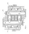
- FIG. 10illustrates a low-field toroidal plasma source 450 according to the present invention that includes a segmented plasma chamber that has relatively low surface erosion.
- the presence of energetic ions in the plasma chambercauses erosion of the inner surface of the plasma chamber.
- the reactivity of the activated and ionized gasesincreases rapidly with their energy. This erosion can contaminate the process. Therefore, it is desirable to reduce the creation of energetic ions and atoms.
- One advantage of the toroidal plasma source of one embodiment of the present inventionis that relatively low electric fields can drive the plasma. Typical electric field intensity are under 10 V/cm. Consequently, the toroidal plasma source of one embodiment of the present invention generates plasmas with low ion energies. Therefore, the surface erosion due to ion bombardment even with highly corrosive gases is relatively low.
- the plasma source of the present inventionincludes a plasma chamber that is formed of metal or a coated-metal
- electric fieldsare induced on the plasma chamber itself
- the voltage induced on the metal plasma chamber bodyappears at the ends of the metal chamber body across the dielectric region 110 ( FIG. 3 ).
- the plasma secondaryis a continuous medium. There is no corresponding abrupt potential change along the toroidal plasma. This disparity in electric potential between the metal plasma chamber and the plasma secondary creates high surface electric fields between the plasma and the metal chamber. The high surface electric fields create energetic ions that may cause surface erosion.
- the threshold energy for ion sputtering for most commonly used materialsis approximately between 20-60 eV. Sputtering damage to the plasma channel surface may become significant when the potential difference across one dielectric gap exceeds 50-100 V.
- the plasma source 450 of FIG. 10includes a plasma chamber 452 that is segmented with multiple dielectric gaps to reduce the potential disparity between the plasma and the metal plasma chamber.
- the plasma chamber 452is segmented into four parts by two dielectric gaps 454 a , 454 b , 454 c and 454 d .
- the plasma chamber 452includes a first 452 a , second 452 b , third 452 c , and fourth chamber 452 d that is segmented by a first 454 a , second 454 b , third 454 c and fourth dielectric gap 454 d .
- the plasma chamber 452is segmented in any number of chambers.
- the plasma source 450includes a transformer core for at least one of the plasma chamber segments.
- the plasma source 450includes a transformer core for each of the plasma chamber segments.
- the plasma source 450includes a first 456 a , second 456 b , third 456 c , and fourth transformer core 456 d .
- the chambers 452are grounded to an enclosure 458 in a way that there is one of dielectric gaps 454 a , 454 b , 454 c , 454 d in a grounded path that circulates one quadrant of the returning magnetic flux contained in transformer core 456 a , 456 b , 456 c or 456 d .
- the voltage on each dielectric gap 454 a , 454 b , 454 c , 454 dis then a quarter of the voltage on the toroidal plasma.
- the plasma loop voltageis distributed across any number of dielectric gaps.
- the segmented plasma chamber 452distributes the induced electric field on the plasma chamber 452 .
- the use of multiple dielectric gapsallows operating a plasma source at significantly higher loop voltages, while reducing or eliminating the plasma channel surface erosion.
- the electric voltage across each of dielectric regions 454 a , 454 b , 454 c , 454 dis reduced to ⁇ 100 V or lower.
- the distribution of loop voltage across multiple dielectric regions 454 a , 454 b , 454 c , 454 dhas been shown to greatly reduce surface erosion.
- circuit elementssuch as resistors and capacitors can be used as voltage dividers in the segmented plasma chamber 452 .
- the use of circuit elements to control the voltage distributionhas some advantages.
- One advantage of using circuit elements to control the voltage distributionis that the voltage division across the dielectric gaps 454 a , 454 b , 454 c , 454 d can be controlled.
- Advantage of using circuit elements to control the voltage distributionis that the electric potential between the plasma and plasma chamber 452 can be minimized even if the dielectric gaps 454 a , 454 b , 454 c , 454 d are not evenly spaced.
- FIG. 11 aillustrates a side view of one embodiment of a low-field toroidal plasma source 500 according to the present invention that includes a quartz plasma chamber 502 and a metal supporting structure 504 .
- FIG. 11 billustrates a center cross section of the low-field toroidal plasma source 500 according to the present invention that includes a quartz plasma chamber 502 and a metal supporting structure 504 .
- the quartz plasma chamber 502is formed in a toroidal geometry.
- the quartz process chamber 502is thermally bonded to a metal structure 504 that provides cooling and mechanical support.
- the metal support 504includes at least one electric gap 506 that prevents induced current flow from forming in the plasma chamber.
- a high thermal conductivity bonding material 508may be used to bond the quartz plasma chamber 502 to the metal structure 504 .
- the bonding materialsmay have a low mechanical hardness to accommodate thermal mismatch between the quartz plasma chamber 502 and the support structure 504 .
- the plasma chamber 502includes a gas inlet 510 and a gas outlet 512 .
- quartz flanges 514are bonded to the quartz plasma chamber 502 near the gas inlet 510 and the gas outlet 512 . Quartz flanges 514 are advantageous because in some applications o-ring seals cannot be used to directly seal the inlet and outlet tube. This is because quartz is not a good thermal conductor.
- a large amount of heatis carried by the process gas as it exits the plasma chamber 502 at the outlet 512 .
- the quartz tube at the outlet 512 of the plasma chamber 502may experience temperatures that are too hot to use an o-ring to seal at the outlet 512 .
- the bonded quartz flanges 514move the vacuum seal surface away from the plasma chamber 502 .
- One side of the quartz flange 514is cooled through the thermal bonding material 508 and the metal structure 504 . This provides a cooled surface for vacuum o-ring seal.
- the plasma source 500includes a high permeability magnetic core 516 that surrounds a portion of the plasma chamber 502 .
- at least two magnetic coressurround at least two portions of the plasma chamber 502 .
- a primary coilsurrounds the magnetic core 516 .
- a circuit containing switching semiconductor devicessupplies a current to the primary winding as described herein. The circuit induces a potential inside the plasma chamber 502 that couples electromagnetic energy to a plasma so as to form a secondary circuit of the transformer as described herein.
- FIG. 11 cillustrates an off center cross section of the low-field toroidal plasma source 500 according to the present invention that includes a quartz plasma chamber 502 and a metal supporting structure 504 .
- the off center cross sectionillustrates the cooling channels 518 in the metal structure 504 that cool the quartz plasma chamber 502 .
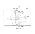
- FIG. 12is a schematic representation of an apparatus 1200 for processing metal bearing gases or silicon bearing gases that embodies the invention.
- the apparatusincludes a gas source 1204 (e.g., a metal bearing gas source) connected via a gas line 1208 to a plasma chamber 1212 .
- a valve 1216controls the flow of a metal bearing gas (e.g., WF 6 and UF 6 ) from the metal bearing gas source 1204 through the gas line 1208 and into the plasma chamber 1212 via a gas inlet 1220 .
- the plasma chamberis, for example, the toroidal plasma chamber 100 of FIG. 3 .
- the apparatusalso includes a plasma gas source 1224 connected via a gas line 1228 to the plasma chamber 1212 .
- a valve 1232controls the flow of plasma gas (e.g., O 2 , H 2 , H 2 O, N 2 , Ar, NF 3 and He) from the plasma gas source 1224 through the gas line 1228 and into the plasma chamber 1212 via a gas inlet 1236 .
- plasma gase.g., O 2 , H 2 , H 2 O, N 2 , Ar, NF 3 and He
- gas sourcesgas lines and gas inlets
- a single gas linecan be used to deliver gases to the plasma chamber 1212 in one embodiment where multiple gas sources are operably connected to the gas line.
- an operatorcan control a valve to select between each of the gas sources to provide an appropriate flow of a specific gas to the plasma chamber at an appropriate point in the process.
- there are no valves and the gas sourcesfor example, control the flow of gas to the plasma chamber.
- gasesare contemplated in alternative embodiments of the invention.
- the gas source 1204can provide, for example, a metal bearing gas or a silicon bearing gas.
- the apparatusalso includes a plasma generator 1240 that generates a plasma within the plasma chamber 1212 .
- the plasma generator 1240is a toroidal low-field gas source, for example, the toroidal low-field gas source of FIG. 1 .
- a controller 1244controls the operation of the plasma generator 1240 which ignites and provides power to a toroidal plasma formed in the plasma chamber 1212 , similarly as previously described herein.
- the plasma generator 1240ignites the plasma gas provided by the plasma gas source 1224 to form the toroidal plasma.
- the plasma chamber 1212can be, for example, formed from a metallic material or can be formed from a dielectric material. In some embodiments, the plasma chamber 1212 includes at least one of a metallic material, coated metallic material or dielectric material. In some embodiments, the plasma chamber 1212 includes a ceramic material or a quartz material.
- the interaction of the toroidal plasma and the metal bearing gas provided to the plasma chamber 1212 by the gas source 1204produces another material.
- the material produceddepends on a number of factors (e.g., power in the toroidal plasma, the type of metal bearing gas, and the types of plasma gases).
- the toroidal plasmais formed from H 2 and reacts with the metal bearing gas to produce a metallic material comprising molecules of the metal atoms contained in the metal bearing gas.
- H 2 O and O 2are used to form the toroidal plasma which reacts with the metal bearing gas to produce a metallic oxide.
- N 2is used to form the toroidal plasma which reacts with the metal bearing gas to produce a metal nitride.
- the apparatus 1200also includes a collection device 1248 that collects the material produced by the interaction of the toroidal plasma with the metal bearing gas.
- the device 1248is connected to an outlet 1252 of the plasma chamber 1212 via a passage 1256 .
- the device 1248collects at least some of the material produced by the interaction between the toroidal plasma and the metal bearing gas that is output from the chamber 1212 .
- Material (e.g., gases, fluids, particles) not collected by the device 1248passes through the passage 1256 into a receptacle 1262 .
- the metal bearing gascomprises fluorine and the receptacle 1262 collects a gas comprising fluorine as a byproduct of the interaction of the toroidal plasma with the metal bearing gas.
- the receptacle 1262 of the apparatus 1200also has an outlet 1266 .
- the outletcan, for example, exhaust to atmosphere or can be coupled to a pump (not shown).
- the device 1248can be, for example, a filter, particle trap, cyclone trap, electrostatic trap or other suitable device for collecting metallic materials, metallic oxides or metal nitrides produced by the interaction of the toroidal plasma with the metal bearing gas.
- the collection device 1248is located external to the plasma chamber 1212 .
- the collection device 1248could, alternatively, be located within the plasma chamber 1212 or partially within the plasma chamber 1212 .
- the collection device 1248is a replaceable component of the apparatus 1200 .
- the plasma source 1240 and plasma chamber 1212 used in the experimentwere an ASTRONi® remote plasma source manufactured by MKS Instruments, Inc. of Wilmington, Mass.
- the metal bearing gas source 1204provided WF 6 to the plasma chamber 1212 .
- the plasma gas source 1224provided a combination of H 2 and N 2 to the plasma chamber 1212 .
- the plasma generator 1244generated a toroidal plasma from the combination of gases located in the plasma chamber 1212 .
- the toroidal plasmareacted with the WF 6 gas to produce W particles. Some of the W metal particles coated an interior surface of the passage 1256 at the outlet of the plasma chamber 1212 .
- EDSEnergy-dispersive x-ray spectrometric
- the plasma source 1240 and plasma chamber 1212 used in the experimentwere an ASTRONi® remote plasma source manufactured by MKS Instruments, Inc. of Wilmington, Mass.
- the metal bearing gas source 1204provided WF 6 to the plasma chamber 1212 .
- the plasma gas source 1224provided a combination of O 2 and N 2 to the plasma chamber 1212 .
- the plasma generator 1244generated a toroidal plasma from the combination of gases located in the plasma chamber 1212 .
- the toroidal plasmareacted with the WF 6 gas to produce a metallic oxide material, WO 3 .
- Energy-dispersive x-ray spectrometric analysiswas conducted on the oxide material output from the plasma chamber 1212 to verify the presence of tungsten (WO 3 ).
- An exemplary EDS analysis systemis a Noran Quest EDS system sold by Thermo Electron Corporation of Madison, Wis.
Landscapes
- Physics & Mathematics (AREA)
- Engineering & Computer Science (AREA)
- Plasma & Fusion (AREA)
- Chemical & Material Sciences (AREA)
- Analytical Chemistry (AREA)
- Plasma Technology (AREA)
Abstract
Description
Claims (10)
Priority Applications (1)
| Application Number | Priority Date | Filing Date | Title |
|---|---|---|---|
| US13/336,616US8779322B2 (en) | 1997-06-26 | 2011-12-23 | Method and apparatus for processing metal bearing gases |
Applications Claiming Priority (9)
| Application Number | Priority Date | Filing Date | Title |
|---|---|---|---|
| US08/883,281US6150628A (en) | 1997-06-26 | 1997-06-26 | Toroidal low-field reactive gas source |
| US09/659,881US6486431B1 (en) | 1997-06-26 | 2000-09-12 | Toroidal low-field reactive gas source |
| US09/774,165US6924455B1 (en) | 1997-06-26 | 2001-01-26 | Integrated plasma chamber and inductively-coupled toroidal plasma source |
| US09/804,650US6815633B1 (en) | 1997-06-26 | 2001-03-12 | Inductively-coupled toroidal plasma source |
| US10/837,912US7166816B1 (en) | 1997-06-26 | 2004-05-03 | Inductively-coupled torodial plasma source |
| US62583804P | 2004-11-08 | 2004-11-08 | |
| US11/269,917US7569790B2 (en) | 1997-06-26 | 2005-11-08 | Method and apparatus for processing metal bearing gases |
| US12/511,785US8124906B2 (en) | 1997-06-26 | 2009-07-29 | Method and apparatus for processing metal bearing gases |
| US13/336,616US8779322B2 (en) | 1997-06-26 | 2011-12-23 | Method and apparatus for processing metal bearing gases |
Related Parent Applications (1)
| Application Number | Title | Priority Date | Filing Date |
|---|---|---|---|
| US12/511,785ContinuationUS8124906B2 (en) | 1997-06-26 | 2009-07-29 | Method and apparatus for processing metal bearing gases |
Publications (2)
| Publication Number | Publication Date |
|---|---|
| US20120160059A1 US20120160059A1 (en) | 2012-06-28 |
| US8779322B2true US8779322B2 (en) | 2014-07-15 |
Family
ID=36205250
Family Applications (1)
| Application Number | Title | Priority Date | Filing Date |
|---|---|---|---|
| US13/336,616Expired - Fee RelatedUS8779322B2 (en) | 1997-06-26 | 2011-12-23 | Method and apparatus for processing metal bearing gases |
Country Status (1)
| Country | Link |
|---|---|
| US (1) | US8779322B2 (en) |
Cited By (10)
| Publication number | Priority date | Publication date | Assignee | Title |
|---|---|---|---|---|
| US20130160523A1 (en)* | 2010-10-06 | 2013-06-27 | RUHR-UNIVERSITäT BOCHUM | Device and use of the device for measuring the density and/or the electron temperature and/or the collision frequency of a plasma |
| US20140141614A1 (en)* | 2012-11-16 | 2014-05-22 | Taiwan Semiconductor Manufacturing Company, Ltd. | Remote Plasma System and Method |
| US20150282289A1 (en)* | 2014-03-28 | 2015-10-01 | Agilent Technologies, Inc. | Waveguide-based apparatus for exciting and sustaining a plasma |
| US20160157331A1 (en)* | 2014-06-14 | 2016-06-02 | Plusware Corporation | Plasma generating apparatus and on-liquid melting method |
| US20170045460A1 (en)* | 2002-12-12 | 2017-02-16 | Perkinelmer Health Sciences, Inc. | Induction device |
| US9909215B2 (en) | 2013-03-15 | 2018-03-06 | Plasmability, Llc | Method of CVD plasma processing with a toroidal plasma processing apparatus |
| US9994480B2 (en)* | 2015-10-16 | 2018-06-12 | Draka Comteq, B.V. | Method for etching a primary preform |
| US10443150B2 (en) | 2015-05-21 | 2019-10-15 | Plasmability, Llc | Toroidal plasma processing apparatus with a shaped workpiece holder |
| US11189471B2 (en)* | 2020-04-16 | 2021-11-30 | Newpowerplasma Co., Ltd. | High frequency generator having dual outputs and its driving method |
| US20240407075A1 (en)* | 2023-04-10 | 2024-12-05 | Mks Instruments, Inc. | Inverted plasma source |
Families Citing this family (3)
| Publication number | Priority date | Publication date | Assignee | Title |
|---|---|---|---|---|
| CN104046785B (en)* | 2014-04-09 | 2016-06-08 | 中南大学 | The treatment process of a kind of waste and old copper iron base diamond cutter head |
| CA3229072A1 (en) | 2017-01-18 | 2018-08-09 | Shine Technologies, Llc | High power ion beam generator systems and methods |
| WO2020185353A1 (en)* | 2019-03-13 | 2020-09-17 | Applied Materials, Inc. | Plasma ignition circuit |
Citations (204)
| Publication number | Priority date | Publication date | Assignee | Title |
|---|---|---|---|---|
| US2981902A (en) | 1958-06-26 | 1961-04-25 | Telecomm Radlioelectriques Et | Automatic impedance matching device |
| US3054742A (en) | 1956-10-26 | 1962-09-18 | Atomic Energy Authority Uk | Gas discharge apparatus |
| US3109801A (en) | 1957-06-20 | 1963-11-05 | Atomic Energy Authority Uk | Gas discharge apparatus |
| US3278384A (en) | 1965-04-13 | 1966-10-11 | Lenard Andrew | Negative "v" stellarator |
| US3343022A (en) | 1965-03-16 | 1967-09-19 | Lockheed Aircraft Corp | Transpiration cooled induction plasma generator |
| US3433705A (en) | 1968-02-28 | 1969-03-18 | Atomic Energy Commission | Stellarator having multipole magnets |
| US3500118A (en) | 1967-07-17 | 1970-03-10 | Gen Electric | Electrodeless gaseous electric discharge devices utilizing ferrite cores |
| US3509500A (en) | 1966-12-05 | 1970-04-28 | Avco Corp | Automatic digital tuning apparatus |
| US3663361A (en) | 1970-02-17 | 1972-05-16 | Atomic Energy Commission | Nuclear fusion device of the air-core tokamak type |
| US3794941A (en) | 1972-05-08 | 1974-02-26 | Hughes Aircraft Co | Automatic antenna impedance tuner including digital control circuits |
| US3801438A (en) | 1970-04-03 | 1974-04-02 | Atomic Energy Commission | Toroidal apparatus for confining plasma |
| US3906405A (en) | 1974-07-01 | 1975-09-16 | Motorola Inc | Tunable antenna coupling circuit |
| US3935503A (en) | 1973-11-26 | 1976-01-27 | The Kreidl Chemico Physical K.G. | Particle accelerator |
| US3987334A (en) | 1975-01-20 | 1976-10-19 | General Electric Company | Integrally ballasted electrodeless fluorescent lamp |
| US4049940A (en) | 1974-10-31 | 1977-09-20 | Agence Nationale De Valorisation De La Recherche (Anvar) | Devices and methods of using HF waves to energize a column of gas enclosed in an insulating casing |
| US4057462A (en) | 1975-02-26 | 1977-11-08 | The United States Of America As Represented By The United States Energy Research And Development Administration | Radio frequency sustained ion energy |
| US4065369A (en) | 1975-07-18 | 1977-12-27 | Tokyo Shibaura Electric Co., Ltd. | Activated gas reaction apparatus & method |
| US4073680A (en) | 1975-06-26 | 1978-02-14 | The United States Of America As Represented By The United States Department Of Energy | Toroidal band limiter for a plasma containment device |
| US4088926A (en) | 1976-05-10 | 1978-05-09 | Nasa | Plasma cleaning device |
| US4095198A (en) | 1977-01-31 | 1978-06-13 | Gte Sylvania Incorporated | Impedance-matching network |
| US4110595A (en) | 1975-06-19 | 1978-08-29 | The United States Of America As Represented By The United States Department Of Energy | High-frequency plasma-heating apparatus |
| US4112045A (en) | 1972-10-05 | 1978-09-05 | Asahi Kasei Kogyo Kabushiki Kaisha | Separation of uranium isotopes using anion exchangers |
| US4118205A (en) | 1976-11-29 | 1978-10-03 | Wang Chia Gee | Separation of gases |
| US4180763A (en) | 1978-01-25 | 1979-12-25 | General Electric Company | High intensity discharge lamp geometries |
| US4201960A (en) | 1978-05-24 | 1980-05-06 | Motorola, Inc. | Method for automatically matching a radio frequency transmitter to an antenna |
| US4206073A (en) | 1977-03-16 | 1980-06-03 | Hoechst Aktiengesellschaft | Process for separating volatile, radioactive substances obtained in the reprocessing of nuclear fuel |
| US4252609A (en) | 1978-11-24 | 1981-02-24 | The United States Of America As Represented By The United States Department Of Energy | Crossed-field divertor for a plasma device |
| US4263096A (en) | 1976-02-02 | 1981-04-21 | The United States Of America As Represented By The United States Department Of Energy | Toroidal magnet system |
| US4282267A (en) | 1979-09-20 | 1981-08-04 | Western Electric Co., Inc. | Methods and apparatus for generating plasmas |
| US4285800A (en) | 1979-04-18 | 1981-08-25 | Branson International Plasma Corp. | Gas plasma reactor for circuit boards and the like |
| US4292125A (en) | 1978-08-21 | 1981-09-29 | Massachusetts Institute Of Technology | System and method for generating steady state confining current for a toroidal plasma fusion reactor |
| US4292124A (en) | 1978-08-21 | 1981-09-29 | Massachusetts Institute Of Technology | System and method for generating steady state confining current for a toroidal plasma fusion reactor |
| US4324611A (en) | 1980-06-26 | 1982-04-13 | Branson International Plasma Corporation | Process and gas mixture for etching silicon dioxide and silicon nitride |
| US4350578A (en) | 1981-05-11 | 1982-09-21 | International Business Machines Corporation | Cathode for etching |
| US4368092A (en) | 1981-04-02 | 1983-01-11 | The Perkin-Elmer Corporation | Apparatus for the etching for semiconductor devices |
| US4431898A (en) | 1981-09-01 | 1984-02-14 | The Perkin-Elmer Corporation | Inductively coupled discharge for plasma etching and resist stripping |
| US4431901A (en) | 1982-07-02 | 1984-02-14 | The United States Of America As Represented By The United States Department Of Energy | Induction plasma tube |
| US4461954A (en) | 1981-04-20 | 1984-07-24 | Inoue-Japax Research Incorporated | Ion-processing method and apparatus |
| US4486722A (en) | 1982-02-18 | 1984-12-04 | Rockwell International Corporation | Pin diode switched impedance matching network having diode driver circuits transparent to RF potential |
| US4486723A (en) | 1983-01-06 | 1984-12-04 | Rca Corporation | Diode switching system for a selectable impedance matching network |
| US4546611A (en) | 1983-12-21 | 1985-10-15 | Eby Robert S | UF6 -Recovery process utilizing desublimation |
| US4601871A (en) | 1983-05-17 | 1986-07-22 | The United States Of America As Represented By The United States Department Of Energy | Steady state compact toroidal plasma production |
| US4626400A (en) | 1983-06-01 | 1986-12-02 | The United States Of America As Represented By The United States Department Of Energy | Variable control of neutron albedo in toroidal fusion devices |
| US4631105A (en) | 1985-04-22 | 1986-12-23 | Branson International Plasma Corporation | Plasma etching apparatus |
| USH268H (en) | 1984-03-20 | 1987-05-05 | The United States Of America As Represented By The United States Department Of Energy | Elmo bumpy square plasma confinement device |
| US4668366A (en) | 1984-08-02 | 1987-05-26 | The Perkin-Elmer Corporation | Optical figuring by plasma assisted chemical transport and etching apparatus therefor |
| US4668336A (en) | 1985-07-23 | 1987-05-26 | Micronix Corporation | Process for making a mask used in x-ray photolithography |
| US4679007A (en) | 1985-05-20 | 1987-07-07 | Advanced Energy, Inc. | Matching circuit for delivering radio frequency electromagnetic energy to a variable impedance load |
| US4680694A (en) | 1985-04-22 | 1987-07-14 | National Distillers And Chemical Corporation | Ozonator power supply |
| US4689192A (en) | 1983-08-30 | 1987-08-25 | Mitsubishi Denki Kabushiki Kaisha | Nuclear fusion reactor |
| US4732761A (en) | 1985-03-23 | 1988-03-22 | Nippon Telegraph And Telephone Corporation | Thin film forming apparatus and method |
| US4735765A (en) | 1985-11-26 | 1988-04-05 | The United States Of America As Represented By The United States Department Of Energy | Flexible helical-axis stellarator |
| US4748383A (en) | 1985-11-04 | 1988-05-31 | U. S. Philips Corporation | DC-AC converter for igniting and supplying a discharge lamp |
| US4767590A (en) | 1986-04-25 | 1988-08-30 | The United States Of America As Represented By The United States Department Of Energy | Anomalous - viscosity current drive |
| US4769064A (en) | 1988-01-21 | 1988-09-06 | The United States Of America As Represented By The United States Department Of Energy | Method for synthesizing ultrafine powder materials |
| US4777061A (en) | 1987-12-14 | 1988-10-11 | Spectrum Cvd, Inc. | Blanket tungsten deposition for dielectric |
| US4779182A (en) | 1985-06-24 | 1988-10-18 | Metallgesellschaft Ag | Power supply for an electrostatic filter |
| US4780803A (en) | 1986-10-02 | 1988-10-25 | G. H. Industrial S.A. | High frequency generator to be used in induction heating, laser, plasma and the alike |
| EP0291181A2 (en) | 1987-04-21 | 1988-11-17 | The Board Of Trustees Of The Leland Stanford Junior University | Plasma reactor for CVD |
| US4786352A (en) | 1986-09-12 | 1988-11-22 | Benzing Technologies, Inc. | Apparatus for in-situ chamber cleaning |
| USH554H (en) | 1972-03-02 | 1988-12-06 | The United States Of America As Represented By The United States Department Of Energy | Toroidal reactor |
| US4794217A (en) | 1985-04-01 | 1988-12-27 | Qing Hua University | Induction system for rapid heat treatment of semiconductor wafers |
| US4793975A (en) | 1985-05-20 | 1988-12-27 | Tegal Corporation | Plasma Reactor with removable insert |
| US4810933A (en) | 1985-07-05 | 1989-03-07 | Universite De Montreal | Surface wave launchers to produce plasma columns and means for producing plasma of different shapes |
| USH627H (en) | 1985-10-03 | 1989-04-04 | The United States Of America As Represented By The United States Department Of Energy | Spherical torus fusion reactor |
| US4853250A (en) | 1988-05-11 | 1989-08-01 | Universite De Sherbrooke | Process of depositing particulate material on a substrate |
| US4859399A (en) | 1977-10-13 | 1989-08-22 | Fdx Patents Holding Company, N.V. | Modular fusion power apparatus using disposable core |
| US4859908A (en) | 1986-09-24 | 1989-08-22 | Matsushita Electric Industrial Co., Ltd. | Plasma processing apparatus for large area ion irradiation |
| US4861622A (en) | 1985-09-21 | 1989-08-29 | Semiconductor Energy Laboratory Co., Ltd. | Method for forming a film coat on the inside of a depression |
| US4863671A (en) | 1986-06-02 | 1989-09-05 | Hitachi, Ltd. | Plasma confinement system |
| US4878149A (en) | 1986-02-06 | 1989-10-31 | Sorbios Verfahrenstechnische Gerate Und Gmbh | Device for generating ions in gas streams |
| US4877757A (en) | 1987-07-16 | 1989-10-31 | Texas Instruments Incorporated | Method of sequential cleaning and passivating a GaAs substrate using remote oxygen plasma |
| US4897282A (en) | 1986-09-08 | 1990-01-30 | Iowa State University Reserach Foundation, Inc. | Thin film coating process using an inductively coupled plasma |
| US4908492A (en) | 1988-05-11 | 1990-03-13 | Hitachi, Ltd. | Microwave plasma production apparatus |
| US4918031A (en) | 1988-12-28 | 1990-04-17 | American Telephone And Telegraph Company,At&T Bell Laboratories | Processes depending on plasma generation using a helical resonator |
| US4948458A (en) | 1989-08-14 | 1990-08-14 | Lam Research Corporation | Method and apparatus for producing magnetically-coupled planar plasma |
| US4985113A (en) | 1989-03-10 | 1991-01-15 | Hitachi, Ltd. | Sample treating method and apparatus |
| US4996077A (en) | 1988-10-07 | 1991-02-26 | Texas Instruments Incorporated | Distributed ECR remote plasma processing and apparatus |
| US5000771A (en) | 1989-12-29 | 1991-03-19 | At&T Bell Laboratories | Method for manufacturing an article comprising a refractory dielectric body |
| US5008593A (en) | 1990-07-13 | 1991-04-16 | The United States Of America As Represented By The Secretary Of The Air Force | Coaxial liquid cooling of high power microwave excited plasma UV lamps |
| US5016332A (en) | 1990-04-13 | 1991-05-21 | Branson International Plasma Corporation | Plasma reactor and process with wafer temperature control |
| US5030889A (en) | 1989-12-21 | 1991-07-09 | General Electric Company | Lamp ballast configuration |
| US5041760A (en) | 1973-10-24 | 1991-08-20 | Koloc Paul M | Method and apparatus for generating and utilizing a compound plasma configuration |
| US5061838A (en) | 1989-06-23 | 1991-10-29 | Massachusetts Institute Of Technology | Toroidal electron cyclotron resonance reactor |
| US5099100A (en) | 1974-08-16 | 1992-03-24 | Branson International Plasma Corporation | Plasma etching device and process |
| US5106827A (en) | 1989-09-18 | 1992-04-21 | The Perkin Elmer Corporation | Plasma assisted oxidation of perovskites for forming high temperature superconductors using inductively coupled discharges |
| US5130003A (en) | 1990-06-14 | 1992-07-14 | Conrad Richard H | method of powering corona discharge in ozone generators |
| US5144196A (en) | 1991-06-12 | 1992-09-01 | Leybold Aktiengesellschaft | Particle source, especially for reactive ionic etching and plasma-supported CVD processes |
| US5153484A (en) | 1991-10-31 | 1992-10-06 | General Electric Company | Electrodeless high intensity discharge lamp excitation coil and ballast configuration for maximum efficiency |
| US5180150A (en) | 1992-01-24 | 1993-01-19 | Hughes Danbury Optical Systems, Inc. | Apparatus for providing consistent registration of semiconductor wafers |
| US5187344A (en) | 1988-11-10 | 1993-02-16 | Agency Of Industrial Science And Technology | Apparatus for decomposing halogenated organic compound |
| US5187454A (en) | 1992-01-23 | 1993-02-16 | Applied Materials, Inc. | Electronically tuned matching network using predictor-corrector control system |
| US5198718A (en) | 1989-03-06 | 1993-03-30 | Nordiko Limited | Filamentless ion source for thin film processing and surface modification |
| US5200595A (en) | 1991-04-12 | 1993-04-06 | Universite De Sherbrooke | High performance induction plasma torch with a water-cooled ceramic confinement tube |
| US5206516A (en) | 1991-04-29 | 1993-04-27 | International Business Machines Corporation | Low energy, steered ion beam deposition system having high current at low pressure |
| US5238532A (en) | 1992-02-27 | 1993-08-24 | Hughes Aircraft Company | Method and apparatus for removal of subsurface damage in semiconductor materials by plasma etching |
| US5254830A (en) | 1991-05-07 | 1993-10-19 | Hughes Aircraft Company | System for removing material from semiconductor wafers using a contained plasma |
| US5277751A (en) | 1992-06-18 | 1994-01-11 | Ogle John S | Method and apparatus for producing low pressure planar plasma using a coil with its axis parallel to the surface of a coupling window |
| US5280154A (en) | 1992-01-30 | 1994-01-18 | International Business Machines Corporation | Radio frequency induction plasma processing system utilizing a uniform field coil |
| US5285372A (en) | 1991-10-23 | 1994-02-08 | Henkel Corporation | Power supply for an ozone generator with a bridge inverter |
| US5291415A (en) | 1991-12-13 | 1994-03-01 | Hughes Aircraft Company | Method to determine tool paths for thinning and correcting errors in thickness profiles of films |
| US5290382A (en) | 1991-12-13 | 1994-03-01 | Hughes Aircraft Company | Methods and apparatus for generating a plasma for "downstream" rapid shaping of surfaces of substrates and films |
| US5298103A (en) | 1993-07-15 | 1994-03-29 | Hughes Aircraft Company | Electrode assembly useful in confined plasma assisted chemical etching |
| US5303139A (en) | 1991-07-31 | 1994-04-12 | Magtron Magneto Elektronische Gerate Gmbh | Low frequency, pulsed, bipolar power supply for a plasma chamber |
| US5336355A (en) | 1991-12-13 | 1994-08-09 | Hughes Aircraft Company | Methods and apparatus for confinement of a plasma etch region for precision shaping of surfaces of substances and films |
| US5346578A (en) | 1992-11-04 | 1994-09-13 | Novellus Systems, Inc. | Induction plasma source |
| US5353314A (en) | 1991-09-30 | 1994-10-04 | The United States Of America As Represented By The United States Department Of Energy | Electric field divertor plasma pump |
| US5352249A (en) | 1992-08-28 | 1994-10-04 | Hughes Aircraft Company | Apparatus for providing consistent, non-jamming registration of semiconductor wafers |
| JPH06291067A (en) | 1993-04-06 | 1994-10-18 | Nippon Steel Corp | Method for forming tungsten film and tungsten CVD apparatus |
| US5359180A (en) | 1992-10-02 | 1994-10-25 | General Electric Company | Power supply system for arcjet thrusters |
| US5364496A (en) | 1993-08-20 | 1994-11-15 | Hughes Aircraft Company | Highly durable noncontaminating surround materials for plasma etching |
| RU2022917C1 (en) | 1989-09-27 | 1994-11-15 | Уланов Игорь Максимович | Process of preparing nitrogen oxide |
| US5365147A (en) | 1990-11-28 | 1994-11-15 | Nichimen Kabushiki Kaisha | Plasma stabilizing apparatus employing feedback controls |
| US5364600A (en) | 1990-11-02 | 1994-11-15 | Sorbios Gmbh | Apparatus for producing ozone from oxygen |
| US5372674A (en) | 1993-05-14 | 1994-12-13 | Hughes Aircraft Company | Electrode for use in a plasma assisted chemical etching process |
| US5376224A (en) | 1992-02-27 | 1994-12-27 | Hughes Aircraft Company | Method and apparatus for non-contact plasma polishing and smoothing of uniformly thinned substrates |
| US5394061A (en) | 1993-01-14 | 1995-02-28 | Adtec Co., Ltd. | High frequency plasma power source and impedance matching device for supplying power to a semiconductor processing apparatus |
| US5397962A (en) | 1992-06-29 | 1995-03-14 | Texas Instruments Incorporated | Source and method for generating high-density plasma with inductive power coupling |
| US5401350A (en) | 1993-03-08 | 1995-03-28 | Lsi Logic Corporation | Coil configurations for improved uniformity in inductively coupled plasma systems |
| US5406177A (en) | 1994-04-18 | 1995-04-11 | General Electric Company | Gas discharge lamp ballast circuit with compact starting circuit |
| US5414238A (en) | 1992-10-02 | 1995-05-09 | Martin Marietta Corporation | Resonant power supply for an arcjet thruster |
| US5419803A (en) | 1993-11-17 | 1995-05-30 | Hughes Aircraft Company | Method of planarizing microstructures |
| US5430355A (en) | 1993-07-30 | 1995-07-04 | Texas Instruments Incorporated | RF induction plasma source for plasma processing |
| JPH07187679A (en) | 1993-12-28 | 1995-07-25 | Hitachi Ltd | Uranium enrichment device and uranium enrichment method |
| US5440206A (en) | 1992-06-26 | 1995-08-08 | Tokyo Electron Ltd. | Plasma processing apparatus comprising means for generating rotating magnetic field |
| US5458732A (en) | 1992-04-14 | 1995-10-17 | Texas Instruments Incorporated | Method and system for identifying process conditions |
| US5460689A (en) | 1994-02-28 | 1995-10-24 | Applied Materials, Inc. | High pressure plasma treatment method and apparatus |
| US5468296A (en) | 1993-12-17 | 1995-11-21 | Lsi Logic Corporation | Apparatus for igniting low pressure inductively coupled plasma |
| US5468955A (en) | 1994-12-20 | 1995-11-21 | International Business Machines Corporation | Neutral beam apparatus for in-situ production of reactants and kinetic energy transfer |
| US5472561A (en) | 1993-12-07 | 1995-12-05 | Sematech, Inc. | Radio frequency monitor for semiconductor process control |
| US5473291A (en) | 1994-11-16 | 1995-12-05 | Brounley Associates, Inc. | Solid state plasma chamber tuner |
| US5474648A (en) | 1994-07-29 | 1995-12-12 | Lsi Logic Corporation | Uniform and repeatable plasma processing |
| US5479072A (en) | 1991-11-12 | 1995-12-26 | General Electric Company | Low mercury arc discharge lamp containing neodymium |
| SU957744A1 (en) | 1980-06-09 | 1996-02-10 | Всесоюзный научно-исследовательский, проектно-конструкторский и технологический институт токов высокой частоты им.В.П.Вологдина | Transformer plasma generator |
| RU2056702C1 (en) | 1990-07-09 | 1996-03-20 | Уланов Игорь Максимович | Transformer-type plasmatron |
| US5505780A (en) | 1992-03-18 | 1996-04-09 | International Business Machines Corporation | High-density plasma-processing tool with toroidal magnetic field |
| US5506507A (en) | 1992-09-18 | 1996-04-09 | Sorbios Verfahrenstechnische Gerate Und Systeme Gmbh | Apparatus for measuring ions in a clean room gas flow using a spherical electrode |
| DE3942560C2 (en) | 1989-12-22 | 1996-05-02 | Dressler Hochfrequenztechnik G | High frequency generator for a plasma generating consumer |
| US5515167A (en) | 1994-09-13 | 1996-05-07 | Hughes Aircraft Company | Transparent optical chuck incorporating optical monitoring |
| US5514246A (en) | 1994-06-02 | 1996-05-07 | Micron Technology, Inc. | Plasma reactors and method of cleaning a plasma reactor |
| US5534231A (en) | 1990-01-04 | 1996-07-09 | Mattson Technology, Inc. | Low frequency inductive RF plasma reactor |
| US5556549A (en) | 1994-05-02 | 1996-09-17 | Lsi Logic Corporation | Power control and delivery in plasma processing equipment |
| US5563709A (en) | 1994-09-13 | 1996-10-08 | Integrated Process Equipment Corp. | Apparatus for measuring, thinning and flattening silicon structures |
| US5565036A (en) | 1994-01-19 | 1996-10-15 | Tel America, Inc. | Apparatus and method for igniting plasma in a process module |
| US5565247A (en) | 1991-08-30 | 1996-10-15 | Canon Kabushiki Kaisha | Process for forming a functional deposited film |
| US5567268A (en) | 1994-01-31 | 1996-10-22 | Sony Corporation | Plasma processing apparatus and method for carrying out plasma processing by using such plasma processing apparatus |
| US5568015A (en) | 1995-02-16 | 1996-10-22 | Applied Science And Technology, Inc. | Fluid-cooled dielectric window for a plasma system |
| US5567255A (en) | 1994-10-13 | 1996-10-22 | Integrated Process Equipment Corp. | Solid annular gas discharge electrode |
| US5573595A (en) | 1995-09-29 | 1996-11-12 | Lam Research Corporation | Methods and apparatus for generating plasma |
| US5576629A (en) | 1994-10-24 | 1996-11-19 | Fourth State Technology, Inc. | Plasma monitoring and control method and system |
| US5585766A (en) | 1994-10-27 | 1996-12-17 | Applied Materials, Inc. | Electrically tuned matching networks using adjustable inductance elements |
| US5610102A (en) | 1993-11-15 | 1997-03-11 | Integrated Process Equipment Corp. | Method for co-registering semiconductor wafers undergoing work in one or more blind process modules |
| US5618382A (en) | 1989-10-03 | 1997-04-08 | Applied Materials, Inc. | High-frequency semiconductor wafer processing apparatus and method |
| US5630880A (en) | 1996-03-07 | 1997-05-20 | Eastlund; Bernard J. | Method and apparatus for a large volume plasma processor that can utilize any feedstock material |
| US5637279A (en) | 1994-08-31 | 1997-06-10 | Applied Science & Technology, Inc. | Ozone and other reactive gas generator cell and system |
| US5643364A (en) | 1994-11-30 | 1997-07-01 | Applied Materials, Inc. | Plasma chamber with fixed RF matching |
| US5654679A (en) | 1996-06-13 | 1997-08-05 | Rf Power Products, Inc. | Apparatus for matching a variable load impedance with an RF power generator impedance |
| US5662819A (en) | 1994-02-10 | 1997-09-02 | Sony Corporation | Plasma processing method with controlled ion/radical ratio |
| USD384173S (en) | 1996-07-19 | 1997-09-23 | Osram Sylvania Inc. | Electrodeless compact fluorescent lamp |
| US5670881A (en) | 1996-02-09 | 1997-09-23 | Toshiba America, Inc. | Discrete step remotely adjustable matching circuit for MRI RF coils |
| RU2094961C1 (en) | 1989-07-20 | 1997-10-27 | Уланов Игорь Максимович | Transformer-type plasmatron |
| US5681393A (en) | 1995-01-24 | 1997-10-28 | Anelva Corporation | Plasma processing apparatus |
| US5685949A (en) | 1995-01-13 | 1997-11-11 | Seiko Epson Corporation | Plasma treatment apparatus and method |
| US5688415A (en) | 1995-05-30 | 1997-11-18 | Ipec Precision, Inc. | Localized plasma assisted chemical etching through a mask |
| US5700297A (en) | 1992-08-28 | 1997-12-23 | Ipec Precision, Inc. | Apparatus for providing consistent, non-jamming registration of notched semiconductor wafers |
| US5712592A (en) | 1995-03-06 | 1998-01-27 | Applied Materials, Inc. | RF plasma power supply combining technique for increased stability |
| JPH10109019A (en) | 1996-10-02 | 1998-04-28 | Hiroshige Watanabe | Uranium enrichment and other element isotope separation utilizing parametric resonance phenomenon and ultrahigh purity ion source or plasma source |
| US5747935A (en) | 1992-04-16 | 1998-05-05 | Advanced Energy Industries, Inc. | Method and apparatus for stabilizing switch-mode powered RF plasma processing |
| US5756400A (en) | 1995-12-08 | 1998-05-26 | Applied Materials, Inc. | Method and apparatus for cleaning by-products from plasma chamber surfaces |
| US5767628A (en) | 1995-12-20 | 1998-06-16 | International Business Machines Corporation | Helicon plasma processing tool utilizing a ferromagnetic induction coil with an internal cooling channel |
| US5773919A (en) | 1986-10-02 | 1998-06-30 | Electron Power Systems | Electron spiral toroid |
| US5798016A (en) | 1994-03-08 | 1998-08-25 | International Business Machines Corporation | Apparatus for hot wall reactive ion etching using a dielectric or metallic liner with temperature control to achieve process stability |
| US5811022A (en) | 1994-11-15 | 1998-09-22 | Mattson Technology, Inc. | Inductive plasma reactor |
| US5814154A (en) | 1997-01-23 | 1998-09-29 | Gasonics International | Short-coupled-path extender for plasma source |
| US5834905A (en) | 1995-09-15 | 1998-11-10 | Osram Sylvania Inc. | High intensity electrodeless low pressure light source driven by a transformer core arrangement |
| US5868909A (en) | 1997-04-21 | 1999-02-09 | Eastlund; Bernard John | Method and apparatus for improving the energy efficiency for separating the elements in a complex substance such as radioactive waste with a large volume plasma processor |
| US5874012A (en) | 1995-03-16 | 1999-02-23 | Hitachi, Ltd. | Plasma processing apparatus and plasma processing method |
| US5883470A (en) | 1996-02-16 | 1999-03-16 | Ebara Corporation | Fast atomic beam source with an inductively coupled plasma generator |
| US5892198A (en) | 1996-03-29 | 1999-04-06 | Lam Research Corporation | Method of and apparatus for electronically controlling r.f. energy supplied to a vacuum plasma processor and memory for same |
| US5901338A (en) | 1998-06-05 | 1999-05-04 | Starmet Corporation | Method for producing uranium oxide and silicon tetrafluoride from uranium tetrafluoride, silicon, and a gaseous oxide |
| US5914278A (en) | 1997-01-23 | 1999-06-22 | Gasonics International | Backside etch process chamber and method |
| US5918106A (en) | 1998-06-05 | 1999-06-29 | Starmet Corp. | Method for producing uranium oxide and a non-radioactive fluorine compound from uranium tetrafluoride and a solid oxide compound |
| US5965034A (en) | 1995-12-04 | 1999-10-12 | Mc Electronics Co., Ltd. | High frequency plasma process wherein the plasma is executed by an inductive structure in which the phase and anti-phase portion of the capacitive currents between the inductive structure and the plasma are balanced |
| US5998933A (en) | 1998-04-06 | 1999-12-07 | Shun'ko; Evgeny V. | RF plasma inductor with closed ferrite core |
| US6007879A (en) | 1995-04-07 | 1999-12-28 | Advanced Energy Industries, Inc. | Adjustable energy quantum thin film plasma processing system |
| US6033642A (en) | 1999-03-29 | 2000-03-07 | Starmet Corporation | Method for producing silicon tetrafluoride from uranium oxyfluoride |
| US6041735A (en) | 1998-03-02 | 2000-03-28 | Ball Semiconductor, Inc. | Inductively coupled plasma powder vaporization for fabricating integrated circuits |
| US6053810A (en) | 1996-12-23 | 2000-04-25 | Medina; Manuel Sierra | Domestic gas detection and expulsion appliance |
| US6063233A (en) | 1991-06-27 | 2000-05-16 | Applied Materials, Inc. | Thermal control apparatus for inductively coupled RF plasma reactor having an overhead solenoidal antenna |
| US6096281A (en) | 1999-03-29 | 2000-08-01 | Starmet Corporation | Method for producing uranium oxide from uranium oxyfluoride |
| US6150628A (en) | 1997-06-26 | 2000-11-21 | Applied Science And Technology, Inc. | Toroidal low-field reactive gas source |
| US6153164A (en) | 1999-10-04 | 2000-11-28 | Starmet Corporation | Method for producing uranium oxide from uranium tetrafluoride and a phyllosilicate mineral |
| US6164241A (en) | 1998-06-30 | 2000-12-26 | Lam Research Corporation | Multiple coil antenna for inductively-coupled plasma generation systems |
| US6253704B1 (en) | 1995-10-13 | 2001-07-03 | Mattson Technology, Inc. | Apparatus and method for pulsed plasma processing of a semiconductor substrate |
| US6303090B1 (en) | 2000-05-17 | 2001-10-16 | The United States Of America As Represented By The United States Department Of Energy | Conversion of depleted uranium hexafluoride to a solid uranium compound |
| EP1145759A1 (en) | 1995-12-27 | 2001-10-17 | Applied Materials, Inc. | Method and apparatus for reducing perfluorocompound gases from substrate processing equipment emissions |
| US6352677B1 (en) | 1996-06-04 | 2002-03-05 | Alliedsignal, Inc. | Process to produce commercial grade anhydrous hydrogen fluoride (AHF) and uranium oxide from the delfuorination of uranium hexafluoride (UF6) |
| US6424232B1 (en) | 1999-11-30 | 2002-07-23 | Advanced Energy's Voorhees Operations | Method and apparatus for matching a variable load impedance with an RF power generator impedance |
| US6459066B1 (en) | 2000-08-25 | 2002-10-01 | Board Of Regents, The University Of Texas System | Transmission line based inductively coupled plasma source with stable impedance |
| US6872909B2 (en) | 2003-04-16 | 2005-03-29 | Applied Science And Technology, Inc. | Toroidal low-field reactive gas and plasma source having a dielectric vacuum vessel |
| US7193369B2 (en) | 2002-11-11 | 2007-03-20 | Samsung Electronics Co., Ltd. | Method for generating gas plasma |
| US20090068082A1 (en) | 2002-01-02 | 2009-03-12 | Blacklight Power, Inc. | Synthesis and characterization of a highly stable amorphous silicon hydride as the product of a catalytic hydrogen plasma reaction |
| JP5144594B2 (en) | 2008-06-30 | 2013-02-13 | ヤフー株式会社 | Server apparatus, prediction method and program in server apparatus |
| JP5166595B2 (en) | 2011-12-16 | 2013-03-21 | 株式会社藤商事 | Game machine |
- 2011
- 2011-12-23USUS13/336,616patent/US8779322B2/ennot_activeExpired - Fee Related
Patent Citations (215)
| Publication number | Priority date | Publication date | Assignee | Title |
|---|---|---|---|---|
| US3054742A (en) | 1956-10-26 | 1962-09-18 | Atomic Energy Authority Uk | Gas discharge apparatus |
| US3109801A (en) | 1957-06-20 | 1963-11-05 | Atomic Energy Authority Uk | Gas discharge apparatus |
| US2981902A (en) | 1958-06-26 | 1961-04-25 | Telecomm Radlioelectriques Et | Automatic impedance matching device |
| US3343022A (en) | 1965-03-16 | 1967-09-19 | Lockheed Aircraft Corp | Transpiration cooled induction plasma generator |
| US3278384A (en) | 1965-04-13 | 1966-10-11 | Lenard Andrew | Negative "v" stellarator |
| US3509500A (en) | 1966-12-05 | 1970-04-28 | Avco Corp | Automatic digital tuning apparatus |
| US3500118A (en) | 1967-07-17 | 1970-03-10 | Gen Electric | Electrodeless gaseous electric discharge devices utilizing ferrite cores |
| US3433705A (en) | 1968-02-28 | 1969-03-18 | Atomic Energy Commission | Stellarator having multipole magnets |
| US3663361A (en) | 1970-02-17 | 1972-05-16 | Atomic Energy Commission | Nuclear fusion device of the air-core tokamak type |
| US3801438A (en) | 1970-04-03 | 1974-04-02 | Atomic Energy Commission | Toroidal apparatus for confining plasma |
| USH554H (en) | 1972-03-02 | 1988-12-06 | The United States Of America As Represented By The United States Department Of Energy | Toroidal reactor |
| US3794941A (en) | 1972-05-08 | 1974-02-26 | Hughes Aircraft Co | Automatic antenna impedance tuner including digital control circuits |
| US4112045A (en) | 1972-10-05 | 1978-09-05 | Asahi Kasei Kogyo Kabushiki Kaisha | Separation of uranium isotopes using anion exchangers |
| US5041760A (en) | 1973-10-24 | 1991-08-20 | Koloc Paul M | Method and apparatus for generating and utilizing a compound plasma configuration |
| US3935503A (en) | 1973-11-26 | 1976-01-27 | The Kreidl Chemico Physical K.G. | Particle accelerator |
| US3906405A (en) | 1974-07-01 | 1975-09-16 | Motorola Inc | Tunable antenna coupling circuit |
| US5099100A (en) | 1974-08-16 | 1992-03-24 | Branson International Plasma Corporation | Plasma etching device and process |
| US4049940A (en) | 1974-10-31 | 1977-09-20 | Agence Nationale De Valorisation De La Recherche (Anvar) | Devices and methods of using HF waves to energize a column of gas enclosed in an insulating casing |
| US3987334A (en) | 1975-01-20 | 1976-10-19 | General Electric Company | Integrally ballasted electrodeless fluorescent lamp |
| US4057462A (en) | 1975-02-26 | 1977-11-08 | The United States Of America As Represented By The United States Energy Research And Development Administration | Radio frequency sustained ion energy |
| US4110595A (en) | 1975-06-19 | 1978-08-29 | The United States Of America As Represented By The United States Department Of Energy | High-frequency plasma-heating apparatus |
| US4073680A (en) | 1975-06-26 | 1978-02-14 | The United States Of America As Represented By The United States Department Of Energy | Toroidal band limiter for a plasma containment device |
| US4065369A (en) | 1975-07-18 | 1977-12-27 | Tokyo Shibaura Electric Co., Ltd. | Activated gas reaction apparatus & method |
| US4263096A (en) | 1976-02-02 | 1981-04-21 | The United States Of America As Represented By The United States Department Of Energy | Toroidal magnet system |
| US4088926A (en) | 1976-05-10 | 1978-05-09 | Nasa | Plasma cleaning device |
| US4118205A (en) | 1976-11-29 | 1978-10-03 | Wang Chia Gee | Separation of gases |
| US4095198A (en) | 1977-01-31 | 1978-06-13 | Gte Sylvania Incorporated | Impedance-matching network |
| US4206073A (en) | 1977-03-16 | 1980-06-03 | Hoechst Aktiengesellschaft | Process for separating volatile, radioactive substances obtained in the reprocessing of nuclear fuel |
| US4859399A (en) | 1977-10-13 | 1989-08-22 | Fdx Patents Holding Company, N.V. | Modular fusion power apparatus using disposable core |
| US4180763A (en) | 1978-01-25 | 1979-12-25 | General Electric Company | High intensity discharge lamp geometries |
| US4201960A (en) | 1978-05-24 | 1980-05-06 | Motorola, Inc. | Method for automatically matching a radio frequency transmitter to an antenna |
| US4292125A (en) | 1978-08-21 | 1981-09-29 | Massachusetts Institute Of Technology | System and method for generating steady state confining current for a toroidal plasma fusion reactor |
| US4292124A (en) | 1978-08-21 | 1981-09-29 | Massachusetts Institute Of Technology | System and method for generating steady state confining current for a toroidal plasma fusion reactor |
| US4252609A (en) | 1978-11-24 | 1981-02-24 | The United States Of America As Represented By The United States Department Of Energy | Crossed-field divertor for a plasma device |
| US4285800A (en) | 1979-04-18 | 1981-08-25 | Branson International Plasma Corp. | Gas plasma reactor for circuit boards and the like |
| US4282267A (en) | 1979-09-20 | 1981-08-04 | Western Electric Co., Inc. | Methods and apparatus for generating plasmas |
| SU957744A1 (en) | 1980-06-09 | 1996-02-10 | Всесоюзный научно-исследовательский, проектно-конструкторский и технологический институт токов высокой частоты им.В.П.Вологдина | Transformer plasma generator |
| US4324611A (en) | 1980-06-26 | 1982-04-13 | Branson International Plasma Corporation | Process and gas mixture for etching silicon dioxide and silicon nitride |
| US4368092A (en) | 1981-04-02 | 1983-01-11 | The Perkin-Elmer Corporation | Apparatus for the etching for semiconductor devices |
| US4461954A (en) | 1981-04-20 | 1984-07-24 | Inoue-Japax Research Incorporated | Ion-processing method and apparatus |
| US4350578A (en) | 1981-05-11 | 1982-09-21 | International Business Machines Corporation | Cathode for etching |
| US4431898A (en) | 1981-09-01 | 1984-02-14 | The Perkin-Elmer Corporation | Inductively coupled discharge for plasma etching and resist stripping |
| US4486722A (en) | 1982-02-18 | 1984-12-04 | Rockwell International Corporation | Pin diode switched impedance matching network having diode driver circuits transparent to RF potential |
| US4431901A (en) | 1982-07-02 | 1984-02-14 | The United States Of America As Represented By The United States Department Of Energy | Induction plasma tube |
| US4486723A (en) | 1983-01-06 | 1984-12-04 | Rca Corporation | Diode switching system for a selectable impedance matching network |
| US4601871A (en) | 1983-05-17 | 1986-07-22 | The United States Of America As Represented By The United States Department Of Energy | Steady state compact toroidal plasma production |
| US4626400A (en) | 1983-06-01 | 1986-12-02 | The United States Of America As Represented By The United States Department Of Energy | Variable control of neutron albedo in toroidal fusion devices |
| US4689192A (en) | 1983-08-30 | 1987-08-25 | Mitsubishi Denki Kabushiki Kaisha | Nuclear fusion reactor |
| US4546611A (en) | 1983-12-21 | 1985-10-15 | Eby Robert S | UF6 -Recovery process utilizing desublimation |
| USH268H (en) | 1984-03-20 | 1987-05-05 | The United States Of America As Represented By The United States Department Of Energy | Elmo bumpy square plasma confinement device |
| US4668366A (en) | 1984-08-02 | 1987-05-26 | The Perkin-Elmer Corporation | Optical figuring by plasma assisted chemical transport and etching apparatus therefor |
| US4732761A (en) | 1985-03-23 | 1988-03-22 | Nippon Telegraph And Telephone Corporation | Thin film forming apparatus and method |
| US4794217A (en) | 1985-04-01 | 1988-12-27 | Qing Hua University | Induction system for rapid heat treatment of semiconductor wafers |
| US4680694A (en) | 1985-04-22 | 1987-07-14 | National Distillers And Chemical Corporation | Ozonator power supply |
| US4631105A (en) | 1985-04-22 | 1986-12-23 | Branson International Plasma Corporation | Plasma etching apparatus |
| US4793975A (en) | 1985-05-20 | 1988-12-27 | Tegal Corporation | Plasma Reactor with removable insert |
| US4679007A (en) | 1985-05-20 | 1987-07-07 | Advanced Energy, Inc. | Matching circuit for delivering radio frequency electromagnetic energy to a variable impedance load |
| US4779182A (en) | 1985-06-24 | 1988-10-18 | Metallgesellschaft Ag | Power supply for an electrostatic filter |
| US4810933A (en) | 1985-07-05 | 1989-03-07 | Universite De Montreal | Surface wave launchers to produce plasma columns and means for producing plasma of different shapes |
| US4906898A (en) | 1985-07-05 | 1990-03-06 | Universite De Montreal | Surface wave launchers to produce plasma columns and means for producing plasma of different shapes |
| US4668336A (en) | 1985-07-23 | 1987-05-26 | Micronix Corporation | Process for making a mask used in x-ray photolithography |
| US4861622A (en) | 1985-09-21 | 1989-08-29 | Semiconductor Energy Laboratory Co., Ltd. | Method for forming a film coat on the inside of a depression |
| USH627H (en) | 1985-10-03 | 1989-04-04 | The United States Of America As Represented By The United States Department Of Energy | Spherical torus fusion reactor |
| US4748383A (en) | 1985-11-04 | 1988-05-31 | U. S. Philips Corporation | DC-AC converter for igniting and supplying a discharge lamp |
| US4735765A (en) | 1985-11-26 | 1988-04-05 | The United States Of America As Represented By The United States Department Of Energy | Flexible helical-axis stellarator |
| US4878149A (en) | 1986-02-06 | 1989-10-31 | Sorbios Verfahrenstechnische Gerate Und Gmbh | Device for generating ions in gas streams |
| US4767590A (en) | 1986-04-25 | 1988-08-30 | The United States Of America As Represented By The United States Department Of Energy | Anomalous - viscosity current drive |
| US4863671A (en) | 1986-06-02 | 1989-09-05 | Hitachi, Ltd. | Plasma confinement system |
| US4897282A (en) | 1986-09-08 | 1990-01-30 | Iowa State University Reserach Foundation, Inc. | Thin film coating process using an inductively coupled plasma |
| US4786352A (en) | 1986-09-12 | 1988-11-22 | Benzing Technologies, Inc. | Apparatus for in-situ chamber cleaning |
| US4859908A (en) | 1986-09-24 | 1989-08-22 | Matsushita Electric Industrial Co., Ltd. | Plasma processing apparatus for large area ion irradiation |
| US4780803A (en) | 1986-10-02 | 1988-10-25 | G. H. Industrial S.A. | High frequency generator to be used in induction heating, laser, plasma and the alike |
| US5773919A (en) | 1986-10-02 | 1998-06-30 | Electron Power Systems | Electron spiral toroid |
| EP0291181A2 (en) | 1987-04-21 | 1988-11-17 | The Board Of Trustees Of The Leland Stanford Junior University | Plasma reactor for CVD |
| US4913929A (en) | 1987-04-21 | 1990-04-03 | The Board Of Trustees Of The Leland Stanford Junior University | Thermal/microwave remote plasma multiprocessing reactor and method of use |
| US4877757A (en) | 1987-07-16 | 1989-10-31 | Texas Instruments Incorporated | Method of sequential cleaning and passivating a GaAs substrate using remote oxygen plasma |
| US4777061A (en) | 1987-12-14 | 1988-10-11 | Spectrum Cvd, Inc. | Blanket tungsten deposition for dielectric |
| US4769064A (en) | 1988-01-21 | 1988-09-06 | The United States Of America As Represented By The United States Department Of Energy | Method for synthesizing ultrafine powder materials |
| US4908492A (en) | 1988-05-11 | 1990-03-13 | Hitachi, Ltd. | Microwave plasma production apparatus |
| US4853250A (en) | 1988-05-11 | 1989-08-01 | Universite De Sherbrooke | Process of depositing particulate material on a substrate |
| US4996077A (en) | 1988-10-07 | 1991-02-26 | Texas Instruments Incorporated | Distributed ECR remote plasma processing and apparatus |
| US5187344A (en) | 1988-11-10 | 1993-02-16 | Agency Of Industrial Science And Technology | Apparatus for decomposing halogenated organic compound |
| US4918031A (en) | 1988-12-28 | 1990-04-17 | American Telephone And Telegraph Company,At&T Bell Laboratories | Processes depending on plasma generation using a helical resonator |
| US5198718A (en) | 1989-03-06 | 1993-03-30 | Nordiko Limited | Filamentless ion source for thin film processing and surface modification |
| US4985113A (en) | 1989-03-10 | 1991-01-15 | Hitachi, Ltd. | Sample treating method and apparatus |
| US5061838A (en) | 1989-06-23 | 1991-10-29 | Massachusetts Institute Of Technology | Toroidal electron cyclotron resonance reactor |
| RU2094961C1 (en) | 1989-07-20 | 1997-10-27 | Уланов Игорь Максимович | Transformer-type plasmatron |
| US4948458A (en) | 1989-08-14 | 1990-08-14 | Lam Research Corporation | Method and apparatus for producing magnetically-coupled planar plasma |
| US5106827A (en) | 1989-09-18 | 1992-04-21 | The Perkin Elmer Corporation | Plasma assisted oxidation of perovskites for forming high temperature superconductors using inductively coupled discharges |
| RU2022917C1 (en) | 1989-09-27 | 1994-11-15 | Уланов Игорь Максимович | Process of preparing nitrogen oxide |
| US5618382A (en) | 1989-10-03 | 1997-04-08 | Applied Materials, Inc. | High-frequency semiconductor wafer processing apparatus and method |
| US5030889A (en) | 1989-12-21 | 1991-07-09 | General Electric Company | Lamp ballast configuration |
| DE3942560C2 (en) | 1989-12-22 | 1996-05-02 | Dressler Hochfrequenztechnik G | High frequency generator for a plasma generating consumer |
| US5000771A (en) | 1989-12-29 | 1991-03-19 | At&T Bell Laboratories | Method for manufacturing an article comprising a refractory dielectric body |
| US5534231A (en) | 1990-01-04 | 1996-07-09 | Mattson Technology, Inc. | Low frequency inductive RF plasma reactor |
| US5016332A (en) | 1990-04-13 | 1991-05-21 | Branson International Plasma Corporation | Plasma reactor and process with wafer temperature control |
| US5130003A (en) | 1990-06-14 | 1992-07-14 | Conrad Richard H | method of powering corona discharge in ozone generators |
| RU2056702C1 (en) | 1990-07-09 | 1996-03-20 | Уланов Игорь Максимович | Transformer-type plasmatron |
| US5008593A (en) | 1990-07-13 | 1991-04-16 | The United States Of America As Represented By The Secretary Of The Air Force | Coaxial liquid cooling of high power microwave excited plasma UV lamps |
| US5364600A (en) | 1990-11-02 | 1994-11-15 | Sorbios Gmbh | Apparatus for producing ozone from oxygen |
| US5365147A (en) | 1990-11-28 | 1994-11-15 | Nichimen Kabushiki Kaisha | Plasma stabilizing apparatus employing feedback controls |
| US5200595A (en) | 1991-04-12 | 1993-04-06 | Universite De Sherbrooke | High performance induction plasma torch with a water-cooled ceramic confinement tube |
| US5206516A (en) | 1991-04-29 | 1993-04-27 | International Business Machines Corporation | Low energy, steered ion beam deposition system having high current at low pressure |
| US5254830A (en) | 1991-05-07 | 1993-10-19 | Hughes Aircraft Company | System for removing material from semiconductor wafers using a contained plasma |
| US5144196A (en) | 1991-06-12 | 1992-09-01 | Leybold Aktiengesellschaft | Particle source, especially for reactive ionic etching and plasma-supported CVD processes |
| US6063233A (en) | 1991-06-27 | 2000-05-16 | Applied Materials, Inc. | Thermal control apparatus for inductively coupled RF plasma reactor having an overhead solenoidal antenna |
| US5303139A (en) | 1991-07-31 | 1994-04-12 | Magtron Magneto Elektronische Gerate Gmbh | Low frequency, pulsed, bipolar power supply for a plasma chamber |
| US5565247A (en) | 1991-08-30 | 1996-10-15 | Canon Kabushiki Kaisha | Process for forming a functional deposited film |
| US5353314A (en) | 1991-09-30 | 1994-10-04 | The United States Of America As Represented By The United States Department Of Energy | Electric field divertor plasma pump |
| US5285372A (en) | 1991-10-23 | 1994-02-08 | Henkel Corporation | Power supply for an ozone generator with a bridge inverter |
| US5153484A (en) | 1991-10-31 | 1992-10-06 | General Electric Company | Electrodeless high intensity discharge lamp excitation coil and ballast configuration for maximum efficiency |
| US5479072A (en) | 1991-11-12 | 1995-12-26 | General Electric Company | Low mercury arc discharge lamp containing neodymium |
| US5336355A (en) | 1991-12-13 | 1994-08-09 | Hughes Aircraft Company | Methods and apparatus for confinement of a plasma etch region for precision shaping of surfaces of substances and films |
| US5291415A (en) | 1991-12-13 | 1994-03-01 | Hughes Aircraft Company | Method to determine tool paths for thinning and correcting errors in thickness profiles of films |
| US5290382A (en) | 1991-12-13 | 1994-03-01 | Hughes Aircraft Company | Methods and apparatus for generating a plasma for "downstream" rapid shaping of surfaces of substrates and films |
| US5187454A (en) | 1992-01-23 | 1993-02-16 | Applied Materials, Inc. | Electronically tuned matching network using predictor-corrector control system |
| US5180150A (en) | 1992-01-24 | 1993-01-19 | Hughes Danbury Optical Systems, Inc. | Apparatus for providing consistent registration of semiconductor wafers |
| US5280154A (en) | 1992-01-30 | 1994-01-18 | International Business Machines Corporation | Radio frequency induction plasma processing system utilizing a uniform field coil |
| US5376224A (en) | 1992-02-27 | 1994-12-27 | Hughes Aircraft Company | Method and apparatus for non-contact plasma polishing and smoothing of uniformly thinned substrates |
| US5238532A (en) | 1992-02-27 | 1993-08-24 | Hughes Aircraft Company | Method and apparatus for removal of subsurface damage in semiconductor materials by plasma etching |
| US5505780A (en) | 1992-03-18 | 1996-04-09 | International Business Machines Corporation | High-density plasma-processing tool with toroidal magnetic field |
| US5458732A (en) | 1992-04-14 | 1995-10-17 | Texas Instruments Incorporated | Method and system for identifying process conditions |
| US5747935A (en) | 1992-04-16 | 1998-05-05 | Advanced Energy Industries, Inc. | Method and apparatus for stabilizing switch-mode powered RF plasma processing |
| US5277751A (en) | 1992-06-18 | 1994-01-11 | Ogle John S | Method and apparatus for producing low pressure planar plasma using a coil with its axis parallel to the surface of a coupling window |
| US5440206A (en) | 1992-06-26 | 1995-08-08 | Tokyo Electron Ltd. | Plasma processing apparatus comprising means for generating rotating magnetic field |
| US5397962A (en) | 1992-06-29 | 1995-03-14 | Texas Instruments Incorporated | Source and method for generating high-density plasma with inductive power coupling |
| US5700297A (en) | 1992-08-28 | 1997-12-23 | Ipec Precision, Inc. | Apparatus for providing consistent, non-jamming registration of notched semiconductor wafers |
| US5352249A (en) | 1992-08-28 | 1994-10-04 | Hughes Aircraft Company | Apparatus for providing consistent, non-jamming registration of semiconductor wafers |
| US5506507A (en) | 1992-09-18 | 1996-04-09 | Sorbios Verfahrenstechnische Gerate Und Systeme Gmbh | Apparatus for measuring ions in a clean room gas flow using a spherical electrode |
| US5359180A (en) | 1992-10-02 | 1994-10-25 | General Electric Company | Power supply system for arcjet thrusters |
| US5414238A (en) | 1992-10-02 | 1995-05-09 | Martin Marietta Corporation | Resonant power supply for an arcjet thruster |
| US5405480A (en) | 1992-11-04 | 1995-04-11 | Novellus Systems, Inc. | Induction plasma source |
| US5346578A (en) | 1992-11-04 | 1994-09-13 | Novellus Systems, Inc. | Induction plasma source |
| US5394061A (en) | 1993-01-14 | 1995-02-28 | Adtec Co., Ltd. | High frequency plasma power source and impedance matching device for supplying power to a semiconductor processing apparatus |
| US5401350A (en) | 1993-03-08 | 1995-03-28 | Lsi Logic Corporation | Coil configurations for improved uniformity in inductively coupled plasma systems |
| JPH06291067A (en) | 1993-04-06 | 1994-10-18 | Nippon Steel Corp | Method for forming tungsten film and tungsten CVD apparatus |
| US5372674A (en) | 1993-05-14 | 1994-12-13 | Hughes Aircraft Company | Electrode for use in a plasma assisted chemical etching process |
| US5298103A (en) | 1993-07-15 | 1994-03-29 | Hughes Aircraft Company | Electrode assembly useful in confined plasma assisted chemical etching |
| US5430355A (en) | 1993-07-30 | 1995-07-04 | Texas Instruments Incorporated | RF induction plasma source for plasma processing |
| US5364496A (en) | 1993-08-20 | 1994-11-15 | Hughes Aircraft Company | Highly durable noncontaminating surround materials for plasma etching |
| US5610102A (en) | 1993-11-15 | 1997-03-11 | Integrated Process Equipment Corp. | Method for co-registering semiconductor wafers undergoing work in one or more blind process modules |
| US5419803A (en) | 1993-11-17 | 1995-05-30 | Hughes Aircraft Company | Method of planarizing microstructures |
| US5472561A (en) | 1993-12-07 | 1995-12-05 | Sematech, Inc. | Radio frequency monitor for semiconductor process control |
| US5639519A (en) | 1993-12-17 | 1997-06-17 | Lsi Logic Corporation | Method for igniting low pressure inductively coupled plasma |
| US5468296A (en) | 1993-12-17 | 1995-11-21 | Lsi Logic Corporation | Apparatus for igniting low pressure inductively coupled plasma |
| JPH07187679A (en) | 1993-12-28 | 1995-07-25 | Hitachi Ltd | Uranium enrichment device and uranium enrichment method |
| US5565036A (en) | 1994-01-19 | 1996-10-15 | Tel America, Inc. | Apparatus and method for igniting plasma in a process module |
| US5789867A (en) | 1994-01-19 | 1998-08-04 | Tel America, Inc. | Apparatus and method for igniting plasma in a process module |
| US5567268A (en) | 1994-01-31 | 1996-10-22 | Sony Corporation | Plasma processing apparatus and method for carrying out plasma processing by using such plasma processing apparatus |
| US5662819A (en) | 1994-02-10 | 1997-09-02 | Sony Corporation | Plasma processing method with controlled ion/radical ratio |
| US5460689A (en) | 1994-02-28 | 1995-10-24 | Applied Materials, Inc. | High pressure plasma treatment method and apparatus |
| US5798016A (en) | 1994-03-08 | 1998-08-25 | International Business Machines Corporation | Apparatus for hot wall reactive ion etching using a dielectric or metallic liner with temperature control to achieve process stability |
| US5406177A (en) | 1994-04-18 | 1995-04-11 | General Electric Company | Gas discharge lamp ballast circuit with compact starting circuit |
| US5556549A (en) | 1994-05-02 | 1996-09-17 | Lsi Logic Corporation | Power control and delivery in plasma processing equipment |
| US5779849A (en) | 1994-06-02 | 1998-07-14 | Micron Technology, Inc. | Plasma reactors and method of cleaning a plasma reactor |
| US5514246A (en) | 1994-06-02 | 1996-05-07 | Micron Technology, Inc. | Plasma reactors and method of cleaning a plasma reactor |
| US5647913A (en) | 1994-06-02 | 1997-07-15 | Micron Technology, Inc. | Plasma reactors |
| US5474648A (en) | 1994-07-29 | 1995-12-12 | Lsi Logic Corporation | Uniform and repeatable plasma processing |
| US5637279A (en) | 1994-08-31 | 1997-06-10 | Applied Science & Technology, Inc. | Ozone and other reactive gas generator cell and system |
| US5932180A (en) | 1994-08-31 | 1999-08-03 | Applied Science And Technology, Inc. | Ozone and other reactive gas generator cell and system |
| US5563709A (en) | 1994-09-13 | 1996-10-08 | Integrated Process Equipment Corp. | Apparatus for measuring, thinning and flattening silicon structures |
| US5515167A (en) | 1994-09-13 | 1996-05-07 | Hughes Aircraft Company | Transparent optical chuck incorporating optical monitoring |
| US5567255A (en) | 1994-10-13 | 1996-10-22 | Integrated Process Equipment Corp. | Solid annular gas discharge electrode |
| US5939886A (en) | 1994-10-24 | 1999-08-17 | Advanced Energy Industries, Inc. | Plasma monitoring and control method and system |
| US5576629A (en) | 1994-10-24 | 1996-11-19 | Fourth State Technology, Inc. | Plasma monitoring and control method and system |
| US5585766A (en) | 1994-10-27 | 1996-12-17 | Applied Materials, Inc. | Electrically tuned matching networks using adjustable inductance elements |
| US5811022A (en) | 1994-11-15 | 1998-09-22 | Mattson Technology, Inc. | Inductive plasma reactor |
| US5473291A (en) | 1994-11-16 | 1995-12-05 | Brounley Associates, Inc. | Solid state plasma chamber tuner |
| US5643364A (en) | 1994-11-30 | 1997-07-01 | Applied Materials, Inc. | Plasma chamber with fixed RF matching |
| US5468955A (en) | 1994-12-20 | 1995-11-21 | International Business Machines Corporation | Neutral beam apparatus for in-situ production of reactants and kinetic energy transfer |
| US5685949A (en) | 1995-01-13 | 1997-11-11 | Seiko Epson Corporation | Plasma treatment apparatus and method |
| US5681393A (en) | 1995-01-24 | 1997-10-28 | Anelva Corporation | Plasma processing apparatus |
| US5568015A (en) | 1995-02-16 | 1996-10-22 | Applied Science And Technology, Inc. | Fluid-cooled dielectric window for a plasma system |
| US5712592A (en) | 1995-03-06 | 1998-01-27 | Applied Materials, Inc. | RF plasma power supply combining technique for increased stability |
| US5874012A (en) | 1995-03-16 | 1999-02-23 | Hitachi, Ltd. | Plasma processing apparatus and plasma processing method |
| US6007879A (en) | 1995-04-07 | 1999-12-28 | Advanced Energy Industries, Inc. | Adjustable energy quantum thin film plasma processing system |
| US5688415A (en) | 1995-05-30 | 1997-11-18 | Ipec Precision, Inc. | Localized plasma assisted chemical etching through a mask |
| US5834905A (en) | 1995-09-15 | 1998-11-10 | Osram Sylvania Inc. | High intensity electrodeless low pressure light source driven by a transformer core arrangement |
| US5573595A (en) | 1995-09-29 | 1996-11-12 | Lam Research Corporation | Methods and apparatus for generating plasma |
| US6253704B1 (en) | 1995-10-13 | 2001-07-03 | Mattson Technology, Inc. | Apparatus and method for pulsed plasma processing of a semiconductor substrate |
| US5965034A (en) | 1995-12-04 | 1999-10-12 | Mc Electronics Co., Ltd. | High frequency plasma process wherein the plasma is executed by an inductive structure in which the phase and anti-phase portion of the capacitive currents between the inductive structure and the plasma are balanced |
| US5756400A (en) | 1995-12-08 | 1998-05-26 | Applied Materials, Inc. | Method and apparatus for cleaning by-products from plasma chamber surfaces |
| US5767628A (en) | 1995-12-20 | 1998-06-16 | International Business Machines Corporation | Helicon plasma processing tool utilizing a ferromagnetic induction coil with an internal cooling channel |
| EP1145759A1 (en) | 1995-12-27 | 2001-10-17 | Applied Materials, Inc. | Method and apparatus for reducing perfluorocompound gases from substrate processing equipment emissions |
| US5670881A (en) | 1996-02-09 | 1997-09-23 | Toshiba America, Inc. | Discrete step remotely adjustable matching circuit for MRI RF coils |
| US5883470A (en) | 1996-02-16 | 1999-03-16 | Ebara Corporation | Fast atomic beam source with an inductively coupled plasma generator |
| US5630880A (en) | 1996-03-07 | 1997-05-20 | Eastlund; Bernard J. | Method and apparatus for a large volume plasma processor that can utilize any feedstock material |
| US5892198A (en) | 1996-03-29 | 1999-04-06 | Lam Research Corporation | Method of and apparatus for electronically controlling r.f. energy supplied to a vacuum plasma processor and memory for same |
| US6352677B1 (en) | 1996-06-04 | 2002-03-05 | Alliedsignal, Inc. | Process to produce commercial grade anhydrous hydrogen fluoride (AHF) and uranium oxide from the delfuorination of uranium hexafluoride (UF6) |
| US5654679A (en) | 1996-06-13 | 1997-08-05 | Rf Power Products, Inc. | Apparatus for matching a variable load impedance with an RF power generator impedance |
| USD384173S (en) | 1996-07-19 | 1997-09-23 | Osram Sylvania Inc. | Electrodeless compact fluorescent lamp |
| JPH10109019A (en) | 1996-10-02 | 1998-04-28 | Hiroshige Watanabe | Uranium enrichment and other element isotope separation utilizing parametric resonance phenomenon and ultrahigh purity ion source or plasma source |
| US6053810A (en) | 1996-12-23 | 2000-04-25 | Medina; Manuel Sierra | Domestic gas detection and expulsion appliance |
| US5914278A (en) | 1997-01-23 | 1999-06-22 | Gasonics International | Backside etch process chamber and method |
| US5814154A (en) | 1997-01-23 | 1998-09-29 | Gasonics International | Short-coupled-path extender for plasma source |
| US5868909A (en) | 1997-04-21 | 1999-02-09 | Eastlund; Bernard John | Method and apparatus for improving the energy efficiency for separating the elements in a complex substance such as radioactive waste with a large volume plasma processor |
| US6150628A (en) | 1997-06-26 | 2000-11-21 | Applied Science And Technology, Inc. | Toroidal low-field reactive gas source |
| US20040079287A1 (en) | 1997-06-26 | 2004-04-29 | Applied Science & Technology, Inc. | Toroidal low-field reactive gas source |
| JP2002507315A (en) | 1997-06-26 | 2002-03-05 | アプライド サイエンス アンド テクノロジー,インコーポレイテッド | Toroidal low-field reactive gas source |
| US6041735A (en) | 1998-03-02 | 2000-03-28 | Ball Semiconductor, Inc. | Inductively coupled plasma powder vaporization for fabricating integrated circuits |
| US5998933A (en) | 1998-04-06 | 1999-12-07 | Shun'ko; Evgeny V. | RF plasma inductor with closed ferrite core |
| US5918106A (en) | 1998-06-05 | 1999-06-29 | Starmet Corp. | Method for producing uranium oxide and a non-radioactive fluorine compound from uranium tetrafluoride and a solid oxide compound |
| US5901338A (en) | 1998-06-05 | 1999-05-04 | Starmet Corporation | Method for producing uranium oxide and silicon tetrafluoride from uranium tetrafluoride, silicon, and a gaseous oxide |
| US6164241A (en) | 1998-06-30 | 2000-12-26 | Lam Research Corporation | Multiple coil antenna for inductively-coupled plasma generation systems |
| US6033642A (en) | 1999-03-29 | 2000-03-07 | Starmet Corporation | Method for producing silicon tetrafluoride from uranium oxyfluoride |
| US6096281A (en) | 1999-03-29 | 2000-08-01 | Starmet Corporation | Method for producing uranium oxide from uranium oxyfluoride |
| US6153164A (en) | 1999-10-04 | 2000-11-28 | Starmet Corporation | Method for producing uranium oxide from uranium tetrafluoride and a phyllosilicate mineral |
| US6424232B1 (en) | 1999-11-30 | 2002-07-23 | Advanced Energy's Voorhees Operations | Method and apparatus for matching a variable load impedance with an RF power generator impedance |
| US6303090B1 (en) | 2000-05-17 | 2001-10-16 | The United States Of America As Represented By The United States Department Of Energy | Conversion of depleted uranium hexafluoride to a solid uranium compound |
| US6459066B1 (en) | 2000-08-25 | 2002-10-01 | Board Of Regents, The University Of Texas System | Transmission line based inductively coupled plasma source with stable impedance |
| US20090068082A1 (en) | 2002-01-02 | 2009-03-12 | Blacklight Power, Inc. | Synthesis and characterization of a highly stable amorphous silicon hydride as the product of a catalytic hydrogen plasma reaction |
| US7193369B2 (en) | 2002-11-11 | 2007-03-20 | Samsung Electronics Co., Ltd. | Method for generating gas plasma |
| US6872909B2 (en) | 2003-04-16 | 2005-03-29 | Applied Science And Technology, Inc. | Toroidal low-field reactive gas and plasma source having a dielectric vacuum vessel |
| JP5144594B2 (en) | 2008-06-30 | 2013-02-13 | ヤフー株式会社 | Server apparatus, prediction method and program in server apparatus |
| JP5166595B2 (en) | 2011-12-16 | 2013-03-21 | 株式会社藤商事 | Game machine |
Non-Patent Citations (181)
| Title |
|---|
| "An Intelligent Solution to RF Load-Power Variability," vol. 2, No. 3, 3rd Quarter (1995) pp. 1-8. |
| "International Lighting Review, Induction Lighting," The Global Lighting Magazine, Apr. 1996. |
| "Linear Circuit Analysis," Electrical Engineering Handbook, (Copyright 1993) pp. 85. |
| "Principals and Techniques," Electrical Engineers' Handbook, (Copyright 1997) pp. 3.40-3.41. |
| "Summary of the Engineering Analysis Report for the Long-term Management of Depleted Uranium Hexafluoride," Work performed under the auspices of the U.S. Department of Energy by Lawrence Livermore National Laboratory under Contract W-7405-ENG-48, UCRL-ID-124080, Sep. 1997 (105 pages). |
| "The Advanced Energy PE 2500 W, 100 kHz Generator with Load Matching User Manual," Sep. 1989. |
| Advanced Energy Industries, Inc., Presentation "Advances in 13.56 MHz Applications" by Knipp (date unknown) pp. 1-32. |
| Advanced Energy Marketing Materials, "Impedance Matching," (Copyright 1992) pp. 1-8. |
| Advanced Energy Marketing Materials, "Introducing Power Supplies and Plasma Systems," (Copyright 1992) pp. 1-8. |
| Akulina et al., "Injection and Confinement of Plasma in a Stellarator with a Multipolar (1=2) Helical Field," Proceedings of Conference of International Atomic Energy Agency (1965) pp. 733-749. |
| Amended Complaint and Jury Demand, filed in the United States District Court for the District of Colorado, by Advanced Energy Industries, Inc., dated Dec. 15, 2003. |
| Anderson, "Electrodeless Fluorescent Lamps Excited by Solenoidal Electric Field," IES Transaction, Illuminating Engineering (Apr. 1969) pp. 236-242. |
| Answer, filed in the United States District Court for the District of Delaware, by Advanced Energy Industries, Inc., dated Dec. 10, 2003. |
| Ashida et al., "Measurements of Pulsed-Power Modulated Argon Plasmas in an Inductively Coupled Plasma Source," J. Vac. Sci. Technol., (Mar./Apr. 1996) pp. 391-397. |
| Asmussen, "Electron Cyclotron Resonance Microwave Discharges for Etching and Thin-Film Deposition," Journal of Vacuum Science & Technology A: Vacuum, Surfaces, and Films, vol. 7, No. 3 (May 1989) pp. 883-893. Abstract printed from Online Journal Publishing Service. |
| Bacri et al., "Influence of Departures From Complete Thermodynamic Equilibrium on Transport Coefficient Values: Application to an Oxygen Plasma," Plasma Sources Sci. Technol., (1994) pp. 114-121. |
| Baldwin et al., "MgF2 Optical Films: Ion-Beam-Assisted Deposition of Magnesium Fluoride in a Conventional Electron Beam Evaporator and the Resulting Film Properties," Society of Vacuum Coaters 40th Annual Technical Conference Proceedings (1997) pp. 1-5. |
| Bell, "Ring Discharge Excitation of Gas Ion Lasers," Applied Physics Letters, vol. 7, No. 7 (Oct. 1965) p. 190. |
| Benesch, Breakdown in the Pretext Tokamak, "Chapter Two—The Machine," Jun. 1981, pp. 15-16. |
| Benova et al., "Axial Distributions of Metastable Atoms and Charged Particles in an Ultrahigh Frequency Argon Plasma Column at Moderate Pressures," J. Appl. Phys., vol. 79, No. 8 (Apr. 15, 1996) pp. 3848-3852. |
| Benova et al., "Theoretical Study of the Influence of a Metal Enclosure on the Parameters of a Plasma Column Sustained by a Traveling Electromagnetic Surface Wave," Physica Scripta, vol. 43 (1991) p. 68-73. |
| Bhave et al., "Two- and Three-Body Ion-Electron Recombination Rate Coefficients in Neon*," Aust. J. Phys., vol. 48 (1995) pp. 503-513. |
| Bishop et al., "Power Balance Measurements and Particle Loss Rate in Ohmically Heated Discharges in the C Stellarator," Plasma Physics and Controlled Nuclear Fusion Research: Proceedings of Second Conference of International Atomic Energy Agency, vol. 2 (1966) pp. 673-685. |
| Bluem et al., "Spatial Investigation of a Large Diameter Microwave Plasma," J. Phys. D: Appl. Phys. vol. 28 (1995) pp. 1529-1533. |
| Böhle et al., "On the Influence of Excited Atoms on the Electron Kinetics of a Surface Wave Sustained Argon Plasma," Plasma Sources Sci. Technol. vol. 3 (1994) pp. 80-87. |
| Boisse-Laporte et al., "Microwave Discharges Produced by Surface Waves in Argon Gas," Journal of Physics D: Applied Physics, vol. 20 (Feb. 14, 1987) p. 197. |
| Bol, "Density Fluctuations in the Etude Stellarator," The Physics of Fluids, vol. 7, No. 11 (Nov. 1964) pp. 1855-1856. |
| Bollinger et al., "Rapid Optical Figuring of Aspherical Surfaces With Plasma Assisted Chemical Etching (PACE)," SPIE vol. 1618 Large Optics II (1991) pp. 14-21. |
| Bollinger et al., "Rapid, Non-Contact Optical Figuring of Aspheric Surfaces With Plasma Assisted Chemical Etching (PACE)," SPIE vol. 1333 Advanced Optical Manufacturing and Testing (1990) pp. 44-57. |
| Bollinger et al., "Rapid, Nonmechanical, Damage-Free Figuring of Optical Surfaces Using Plasma-Assisted Chemical Etching (PACE): Part I Experimental Results," SPIE vol. 966 Advances in Fabrication and Metrology for Optics and Large Optics, (1988) pp. 82-90. |
| Boswell et al., "Etching of Si by SF6 in a Radio Frequency Double Cathode," Journal of Vacuum Science & Technology B: Microelectronics and Nanometer Structures, vol. 5, No. 4 (Jul. 1987) pp. 883-888. Abstract printed from Online Journal Publishing Service. |
| Bourdon et al., "Three-Body Recombination Rate of Atomic Nitrogen in Low-Pressure Plasma Flows," Physical Review E., vol. 54, No. 2 (Aug. 1996) pp. 1888-1898. |
| Carruth, Jr., et al., "Method for Determination of Neutral Atomic Oxygen Flux," Rev. Sci. Instrum., vol. 61, No. 4 (1990) pp. 1211-1216. |
| Cayless et al., "Lamps and Lighting," Third Edition, pp. 280-286. |
| Chen, "Industrial Applications of Low-Temperature Plasma Physics*," Phys. Plasmas, vol. 2, No. 6 (Jun. 1995) pp. 2164-2175. |
| Cherrington, "Chapter 8: DC Discharges-The Positive Column," Gaseous Electronics and Gas Lasers Pergamon Press-New York (1979) pp. 144-160. |
| Chiu et al., "What the DryScrub® System Can Do for PFC Gas Treatment?," Electrochemical Technology Corp. Brochure (undated). |
| Coburn et al., "Ion-and Electron-Assisted Gas-Surface Chemistry-An Important Effect in Plasma Etching," Journal of Applied Physics, vol. 50, No. 5 (May 1979) pp. 3189-3196. Abstract printed from Online Journal Publishing Service. |
| Cohen et al., "Induced Magnetic Field Effects in Inductively Coupled Plasmas," Physics of Plasma, vol. 3, No. 5 (May 1996) pp. 1839-1847. Abstract printed from Online Journal Publishing Service. |
| Collins et al., "Measurement of the Rate Coefficient for the Recombination of He+ with Electrons*," Physical Review A, vol. 6, No. 4 (Oct. 1972) pp. 1545-1558. |
| Complaint for Declaratory Judgment of Non-Infringement, filed in the United States District Court for the District of Colorado, by Advanced Energy Industries, Inc., dated Apr. 3, 2003. |
| Complaint, filed in the United States District Court for the District of Delaware, by MKS Instruments, Inc. and Applied Science and Technology, Inc., dated May 14, 2003. |
| CRC Handbook of Chemistry and Physics (1979-1980) pp. E-60. |
| Darchicourt et al., "Influence of the Radial Electron Density Profile on the Determination of the Characteristics of Surface-Wave-Produced Discharges," J. Phys. D: Applied Physics, vol. 21 (1988) pp. 293-301. |
| Denneman, "Determination of Electromagnetic Properties of Low-Pressure Electrodeless Inductive Discharges," J. Phys. D: Appl. Phys. (1990) pp. 293-298. |
| Didenko et al., "An Intense Source of Optical Emission from Electrodeless Low-Frequency Discharge in Vapors of Sulfur and Mercury," Doklady Physics, vol. 45, No. 4 (2000) pp. 155-156. |
| E. Kandler et al., "Characterization of Plasma in an Inductively Coupled High-Dense Plasma Source" Surface Coatings & Tech 74 75:539-545 (1995). |
| Eckert, "The Hundred Year History of Induction Discharges," Proceedings of the Second Annual International Conference of Plasma Chemistry and Technology (Nov. 12-13, 1984) pp. 171-202. |
| Eckhartt et al., "Comparison of Alkali Plasma Loss Rates in a Stellarator and in a Toroidal Device With Minimum Mean-B Properties," Plasma Physics and Controlled Nuclear Fusion Research: Proceedings of Second Conference of International Atomic Energy Agency, vol. 2 (1966) pp. 719-731. |
| Evans, "Discussion (of 'Electrodeless Fluorescent Lamps Excited by Solenoidal Electric Field' by Anderson)," IES Transaction, Illuminating Engineering (Apr. 1969) pp. 242-244. |
| F. Maier, "Electronic Circuits for the Generation and Transfer of High-Power Pulses in Nuclear Fusion Installations" IEEE Transactions on Plasma Science PS-12(3): 191-198 (1984). |
| Feoktistov et al., "Self-Consistent Modeling of Low-Pressure RF Discharges in Oxygen Plasma," J. Phys. D: Appl. Phys. vol. 26 (1995) pp. 1346-1353. |
| Ferreira et al., "Quasi-Neutral Theory of Positive Columns in Electronegative Gases," J. Phys. D: Appl. Phys., vol. 21 (1988) pp. 1403-1413. |
| Ferreira, "Kinetic Modeling of Microwave Discharges," Microwave Discharges: Fundamentals and Applications (1993) pp. 313-337. |
| Ferreira, "Modeling of a Low-Pressure Plasma Column Sustained by a Surface Wave," J. Phys. D: Appl. Phys. vol. 16 (1983) p. 1673-1685. |
| Ferreira, "The Similarity Laws for the Maintenance Field and the Absorbed Power per Electron in Low-Pressure Surface Wave Produced Plasmas and their Extension to HF Plasmas in General," Physica Scripta, vol. 38 (1988) pp. 382-399. |
| Ferreira, "Theory of a Plasma Column Sustained by a Surface Wave," J. Phys. D: Appl. Phys. (1981) pp. 1811-1830. |
| Fiala et al., "Two-Dimensional, Hybrid Model of Low-Pressure Glow Discharges," Physical Review E., vol. 49, No. 6 (Jun. 1994) pp. 5607-5622. |
| Foutz, "Switching-Mode Power Supply Design" (Jan. 17, 2001) pp. 1-3. |
| Fulton et al., "Application of Residual Stress Analysis for Ion-Assist-Deposited (IAD) Thin-Films Manufactured Using a Gridless End-Hall Ion Source," Optical Interference Coatings: Technical Digest Series, vol. 17 (1995) pp. 101-103. |
| Fulton, "Application of Ion-Assisted-Deposition Using a Gridless End-Hall Ion Source for Volume Manufacturing of Thin-Film Optical Filters," Optical Interference Coatings: Proceedings-SPIE The International Society for Optical Engineering (1994) pp. 374-393. |
| G. Soucy et al., "Parametric Study of the Decomposition of NH3 for an Induction Plasma Reactor Design" Plasma Chem. and Plasma Prof. 15(4):693-710 (1995). |
| Gale et al., "Characterization of a Micromachined Electrical Field-Flow Fractionation (μEFFF) System" (no date) pp. 1-6. |
| Gallatin et al., "Predicted Polishing Behavior of Plasma Assisted Chemical Etching (PACE) From a Unified Model of the Temporal Evolution of Etched Surfaces," SPIE Advances in Fabrication and Metrology for Optics and Large Optics, vol. 966 (1988) pp. 98-107. |
| Gallatin et al., "Unified Approach to the Temporal Evolution of Surface Profiles in Solid Etch and Deposition Processes," J. Appl. Phys., vol. 65, No. 12 (Jun. 1989) pp. 5078-5088. |
| Golant et al., "Plasma Compression by a Magnetic Field in a Toroidal-Type Device," Proceedings of Conference of International Atomic Energy Agency (1965) pp. 830-850. |
| Goldsborough et al., "RF Induction Excitation of CW Visible Laser Transitions in Ionized Gases," Appl. Phys. Let., vol. 8, No. 6 (Mar. 15, 1966) pp. 137-139. |
| Gousset et al., "Electron and Heavy-Particle Kinetics in the Low Pressure Oxygen Positive Column," J. Phys. D: Appl. Phys., vol. 24 (1991) pp. 290-300. |
| Gousset et al., "Experimental Study of a D.C. Oxygen Glow Discharge by V.U.V. Absorption Spectroscopy," Plasma Chemistry and Plasma Processing vol. 7, No. 4 (1987) pp. 409-427. |
| Granier et al., "Characterisation of Oxygen Discharges," Journal of Physics D: Applied Physics, vol. 22 (1989) pp. 1487-1496. |
| Granier et al., "Diagnostics in O2 Helicon Plasmas for SiO2 Deposition," Plasma Sources Sci. Technol., vol. 6 (1997) pp. 147-156. |
| H.U. Eckert, "An Electrodeless Discharge at 60 Hz" IEEE Trans on Plasma Sci PS-2:308-309 (1974). |
| H.U. Eckert, "Analysis of Thermal Induction Plasmas between Coaxial Cylinders" J Appl Phys 43(1):46-52 (1972). |
| H.U. Eckert, "Induction Plasmas as Low Frequencies" AIAA Journal 9(8):1452-1456 (1971). |
| H.U. Eckert, "The Induction Arc: A State-of-the-Art Review" High Temp Sci 6:99-134 (1974). |
| Hartney et al., "Critical Review: Oxygen Plasma Etching for Resist Stripping and Multilayer Lithography," J. Vac. Sci. Technol., pp. 1 (Jan./Feb. 1989). |
| Heckman et al., Advanced Energy Marketing Materials, "The Evolution of RF Power Delivery in Plasma Processing," (Copyright 1998) pp. 1-8. |
| Heimer et al., "Ponderomotive Transport of Charge in the Induction Plasma," J. Vac. Sci. Technol., (Jan./Feb. 1994) pp. 507-511. |
| Henriksen et al., "Electromagnetic Field in Electrodeless Discharge," Journal of Applied Physics, vol. 42, No. 13 (Dec. 1971) pp. 5460-5464. |
| Herman, "Plasma-Sprayed Coatings," Scientific American (Sep. 1988) pp. 112-117. |
| Heshmaty et al., "Approaches Explored for Producing a Variety of Ion-Assisted-Deposited Thin-Film Coatings Using an End-Hall Ion Source," Developments in Optical Component Coatings: Proceedings of SPIE Conference, vol. 2776 (1996) pp. 114-125. |
| Hiramatsu et al., "Generation of Strongly Ionized Aluminum Plasma in a Low-Temperature Tokamak Discharge," Japanese Journal of Applied Physics, vol. 31 (Jul. 1992) pp. 2243-2248. |
| Hirose et al., "STOR II A Tokamak for Plasma Heating Studies," Plasma Physics Laboratory, University of Saskatchewan, Apr. 1981, pp. 11-14. |
| Hopwood et al., "Electromagnetic Fields in a Radio-Frequency Induction Plasma," Journal of Vacuum Science & Technology A: Vacuum, Surfaces, and Films, vol. 11, No. 1 (Jan. 1993) pp. 147-151. Abstract printed from Online Journal Publishing Service. |
| Hopwood et al., "Langmuir Probe Measurements of a Radio Frequency Induction Plasma," Journal of Vacuum Science & Technology A: Vacuum, Surfaces, and Films, vol. 11, No. 1 (Jan. 1993) pp. 152-156. Abstract printed from Online Journal Publishing Service. |
| Hopwood, "Review of Inductively Coupled Plasmas for Plasma Processing," Plasma Sources Sci. Technol., (1992) pp. 109-116. |
| International Search Report dated Nov. 5, 1998 in corresponding PCT Application No. PCT/US98/13155. |
| Journal of Technical Physics, vol. 33, No. 10 (1963) pp. 1169-1172. (Russian). |
| Kassakian et al., Principles of Power Electronics, 1991, Chapter 1, pp. 1-8. |
| Kita et al., "Rocket Observation of Atomic Oxygen and Night Airglow: Measurement of Concentration with an Improved Resonance Fluorescence Technique," Annales Geophysicae, vol. 14 (1996) 227-237. |
| Kogan et al., "Research into Potential for Creating Transformer Type Plasmatrons," Teplofizika Vysokikh Temperatur, vol. 31, No. 1, 1993, pp. 1-8. |
| Kolobov et al., "Electron Kinetics and Non-Joule Heating in Near-Collisionless Inductively Coupled Plasmas," Physical Review E, vol. 55, No. 3 (Mar. 1997) 3408-3422. |
| Kortshagen et al., "Determination of Electron Energy Distribution Functions in Surface Wave Produced Plasmas: I. Modeling," J. Phys. D: Appl. Phys., vol. 24 (1991) pp. 1571-1584. |
| Kortshagen et al., "Determination of Electron Energy Distribution Functions in Surface Wave Produced Plasmas: II. Measurements," J. Phys. D: Appl. Phys., vol. 24 (1991) pp. 1585-1593. |
| Kortshagen, "Experimental and Theoretical Determination of Electron Energy Distribution Functions in Surface Wave Plasmas," Microwave Discharges: Fundamentals and Applications (1993) pp. 303-312. |
| Kouznetsov et al., "Modeling Electronegative Discharges at Low Pressure," Plasma Sources Science & Technology, vol. 5, No. 4 (Nov. 1996) Abstract printed from Insititue for Scientific Information. |
| Lee et al., "Global Model for High Pressure Electronegative Radio-Frequency Discharges," Journal of Vacuum Science & Technology A-Vacuum Surfaces and Films vol. 15, No. 1 (Jan.-Feb. 1997) 113-126. Abstract printed from Institute for Scientific Information. |
| Lenk, "Switching Power-Supply Basics," Simplified Design of Switching Power Supplies (1995) pp. 1. |
| Lichtenberg et al., "Modeling Plasma Discharges at High Electronegativity," Plasma Sources Sci. Technol. vol. 6 (1997) 437-449. |
| Lieberman et al., Principles of Plasma Discharges and Material Processing; Chapter 12 "Inductive Discharges," pp. 387-389. |
| Lister et al., "Modeling of Inductively Coupled Discharges With Internal and External Coils," Plasma Sources Sci. Technol. vol. 1 (1992) 67-73. |
| Malik et al., "Overview of Plasma Source Ion Implantation Research at University of Wisconsin-Madison," Journal of Vacuum Science & Technology B: Microelectronics and Nanometer Structures vol. 12, No. 2 (Mar. 1994) 843-849. Abstract printed from Online Journal Publishing Service. |
| Margot et al., "Modeling of Surface-Wave-Sustained Plasmas in Static Magnetic Fields: A Tool for the Study of Magnetically Assisted HF Plasmas," Microwave Discharges: Fundamentals and Applications (1993) 141-159. |
| Massey, "Fabric antennas for mobile telephony integrated within clothing" (no date) pp. 1-4. |
| Memorandum Opinion, US District Court for the District of Delaware, dated Apr. 26, 2002. |
| Memorandum Opinion, US District Court for the District of Delaware, dated Feb. 12, 2004. |
| Memorandum Opinion, US District Court for the District of Delaware, dated May 14, 2002. |
| Michelt et al., "Measurement of the Rotational Temperature of Oxygen in a High-Power Inductively Coupled Plasma," J. Phys. D: Appl. Phys. vol. 28 (1995) 2600-2606. |
| Moisan et al., "A Small Microwave Plasma Source for Long Column Production Without Magnetic Field," IEEE Transactions on Plasma Science, vol. PS-3, No. 2 (Jun. 1975) p. 55. |
| Moisan et al., "Plasma Sources Based on the Propagation of Electromagnetic Surface Waves," J. Phys. D: Appl. Phys. vol. 24 (1991) pp. 1025-1048. |
| Morrow et al., "In Situ Measurement of Atomic Nitrogen in the Ground (4S) and Metastable (2D) and (2P) States by Resonance Fluorescence for Project Aries," Centre for Research in Experimental Space Science (Apr. 1981). |
| Niederwald et al., "IAD of Oxide Coatings at Low Temperature: A Comparison of Processes based on Different Ion Sources," Proc. SPIE vol. 3133 (1997) pp. 205-213. |
| Okada et al., "Microwave Determination of the Coefficient of Dissociative Recombination of Ar2 in AR Afterglow," J. Phys. D: Appl. Phys. vol. 26 (1993) 1680-1686. |
| Ono et al., "Effect of Annealing on Mechanical Properties of Electron-Irradiated Aluminum single Crystals at 23° K1,," Applied Physics Letters vol. 7, No. 7 (Oct. 1, 1965) pp. 191. |
| Order, US District Court for the District of Delaware, dated Apr. 26, 2002. |
| Order, US District Court for the District of Delaware, dated Feb. 12, 2004. |
| Order, US District Court for the District of Delaware, dated May 13, 2002. |
| Osram ECG-SPOT Brochure, Feb. 1997, pp. 1-12. |
| Osram Endura 150W Product Information Brochure, Nov. 1996, pp. 1-4. |
| Pawlewicz et al., "Low-Energy High-Flux Reactive Ion Assisted Deposition of Oxide Optical Coatings: Performance, Durability, Stability and Scalability," SPIE Proceedings 2261 (1994) 1-12. |
| Perry et al., "The Application of the Helicon Source of Plasma Processing" Journal of Vacuum Science & Technology B: Microelectronics and Nanometer Structures vol. 9, No. 2 (Mar. 1991) 310-317. Abstract printed from Online Journal Publishing Service. |
| Persson "Brush Cathode Plasma—A Well-Behaved Plasma," Journal of Applied Physics vol. 36, No. 10 (Oct. 1965) 3086-3094. |
| Persson "Inertia-Controlled Ambipolar Diffusion," The Physics of Fluids vol. 5, No. 12 (Dec. 1962) 1625-1632. |
| Phelps "Role of Molecular Ions, Metastable Molecules, and Resonance Radiation in the Breakdown of Rare Gases," The Physical Review vol. 117, No. 3 (Feb. 1, 1960) 619-632. |
| Piejak et al., "A Simple Analysis of an Inductive RF Discharge," Plasma Source, Science and Technology, vol. 1, No. 3 (1992) pp. 179-186. |
| Piejak et al., "The Electric Field and Current Density in a Low-Pressure Inductive Discharge Measured with Different B-dot Probes," J. Appl. Phys. vol. 81, No. 8 (Apr. 15, 1997) 3416-3421. |
| Popov "Characteristics of Electron Cyclotron Resonance Plasma Sources," Journal of Vacuum Science & Technology A: Vacuum, Surfaces, and Films vol. 7, No. 3 (May 1989) 894-898. Abstract printed from Online Journal Publishing Service. |
| Pressman, Switching Power Supply Design, (no date) pp. xvii. |
| Price, "Potential Uses of Depleted Uranium," American Nuclear Society, 2000 International Winter and Embedded Topical Meetings, Washington, D.C., Nov. 12B16, 2000; Jun. 2000 (5 pages). |
| Quapp et al., "New Options for Managing Depleted Uranium Materials," Submitted for Publication to Spectrum 98 (6 pages). |
| R.A. Krakowski et al., "Prospects for Using Low-Frequency Induction Plasmas for Bulk-Chemical Processing: A Systems Analysis" First INEL Workshop on Plasma Applications to Waste Treatment, Idaho Fall, Idaho, Jan. 16-17, 1991. |
| Rapp et al., "Charge Exchange Between Gaseous Ions and Atoms," The Journal of Chemical Physics vol. 37, No. 11 (Dec. 1, 1962) 2631-2645. |
| Remote Plasma Source Chapter 2, (Mar. 2001) pp. 2-1-2-6. |
| Resonance Ltd., Operation Manual for RF Powered Line Sources (undated). |
| Resonance Ltd., Operation Manual for Vacuum Monochromator Model #VS2FS (Sep. 1993). |
| S.V. Dresvin, Physics & Tech. of Low Temp. Plasmas, H. Eckert ed, p. 234 (1977). |
| Sato, "Plasma Density Profile and Electron Temperature in Discharge Positive Columns at Intermediate Pressures: Examination of Ingold's Approximation," J. Phys. D: Appl. Phys. vol. 26 (1993) 1687-1690. |
| Schiffer et al., "Negative-Oxygen-Ion Detection by a Crossed-Beam Photodetachment Technique," Plasma Sources Sci. Technol. vol. 4 (1995) 345-352. |
| Schlier et al., "Production of High-Value Fluoride Gas from Uranium Tetrafluoride Using a Rotary Calciner," WM'01 Conference, Feb. 25-Mar. 1, 2001, Tucson, AZ (12 pages). |
| Self et al., "Static Theory of a Discharge Column at Intermediate Pressures," The Physics of Fluids vol. 9, No. 12 (Dec. 1966) 2486-2492. |
| Sirghi et al., "Nonlocal Particle Loss Effects on the Electron Kinetics in a Direct Current Helium Diffusion-Controlled Positive Column," Phys. Plasmas vol. 4, No. 4 (Apr. 1997) 1160-1165. |
| Smirnov et al., "Resonance Charge Transfer in Inert Gases," Soviet Physics-Technical Physics vol. 10, No. (1965) 83-92. |
| Smith, "Section 9.6: Plasma Chemistry," Thin-Film Deposition: Principles and Practice McGraw-Hill-New York: (1995) pp. 616-617. |
| Smith, "Thin-Film Deposition: Principles and Practice," McGraw Hill, Boston, (1995) pp. 520-525. |
| Stodiek et al., "Plasma Confinement in Low-Density C Stellarator Discharges," Proceedings of a Conference on Plasma Physics and Controlled Nuclear Fusion Research CN-21/120, International Atomic Energy Agency (1965) pp. 687-703. |
| Stowers et al., "Review of Precision Surface Generating Processes and Their Potential Application to the Fabrication of Large Optical Components*," SPIE Advances in Fabrication and Metrology for Optics and Large Optics, vol. 966 (1988) pp. 62-73. |
| Suchel et al., "Properties of TiO2 and SiO2 Films Prepared by Ion-Assisted Deposition Using a Gridless End-Hall Ion Source," Society of Vacuum Coaters: 36th Annual Technical Conference Proceedings (1993) pp. 82-87. |
| Sugai et al., "Diagnostics and Control of Radicals in an Inductively Coupled Etching Reactor," Journal of Vacuum Science & Technology A., Vac. Surf. Films, vol. 13, No. 3, Pt. 1 (May/Jun. 1995) pp. 887-893. |
| T.B. Reed, "Growth of Refractory Crystals Using the Induction Plasma Torch" J. Appl. Phys. 32(12)2534-2535 (1961). |
| T.B. Reed, "Heat-Transfer Intensity from Induction Plasma Flames and Oxy-Hydrogen Flames" J. Appl. Phys. 34(8)2266-2269 (1963). |
| T.B. Reed, "High-Power Low-Density Induction Plasmas" Communications 3146-3147 (1963). |
| T.B. Reed, "Induction-Coupled Plasma Torch" J. Appl. Phys. 32(5):821-824 (1961). |
| Talanov et al., "Measurement of the absolute penetration depth and surface resistance of superconductors and normal metals with the variable spacing parallel plate resonator," Review of Scientific Instruments, vol. 71, No. 5 (May 2000) pp. 2136-2146. |
| Toader "On the Constricted Neon Positive Column," J. Phys. D: Appl. Phys., vol. 28 (1995) 75-80. |
| Tuszewski "An Electronegative Inductive Discharge Instability," J. Appl. Phys. vol. 79, No. 12 (Jun. 15, 1996) 8967-8975. |
| Tuszewski et al., "Composition of the Oxygen Plasmas from Two Inductively Coupled Sources," J. Vac. Sci. Technol. A vol. 13, No. 3 (May/Jun. 1995) 839-842. |
| Tuszewski, "Enhanced Radio Frequency Field Penetration in an Inductively Coupled Plasma," Physical Review Letters vol. 77, No. 7 (Aug. 12, 1996) 1286-1289. |
| Tuszewski, "Inductive Electron Heating Revisited*," Phys. Plasmas vol. 4, No. 5 (May 1997) 1922-1928. |
| Ulanov et al., "Study of the Transformer-Coupled Induction Toroidal Discharge for Development of Plasma-Chemical Reactors and New Light Sources," (date unknown) pp. 1-19. |
| V.A. Kogan et al., "Investigation of the Prospect for the Design of Transformer-Type Plasmotrons" Teplofizika Vysokikh Temperatur 31(1):105-110 (1993). |
| V.M. Gol'dfarb et al., "Properties of a Low-Frequency Discharge in a Transformer Plasmatron" Teplofizika Vysokikh Temperatur 17(4):698-702 (1979). |
| Vahedi "Modeling and Simulation of RF Discharges Used for Plasma Processing," Dissertation Submitted in Partial Satisfaction of Requirement for Ph.D. in Electrical Engineering and Computer Science from University of California at Berkeley (1993). |
| Vahedi et al., "Analytic Model of the Ion Angular Distribution in a Collisional Sheath," Journal of Vacuum Science & Technology A: Vacuum, Surfaces, and Films vol. 11, No. 4 (Jul. 1993) 1275-1282. Abstract printed from Online Journal Publishing Service. |
| Van Hoornich, et al., "Recovery of Tungsten from the Exhaust of a Tungsten Chemical Vapor Deposition Tool," Journal of the Electrochemical Society, 147 (12), 2000, pp. 4665-4670. |
| Vasil'kovskaya et al., "Some Problems of Experimental Investigation of Vortex Flows of Gas in a Cylindrical Channel and Toroidal Chamber," News of the Siberian Division of the USSR Academy of Science, vol. 8, No. 2 (1982). |
| Vi{hacek over (c)}ek, "A Collisional-Rediative Model Applicable to Argon Discharges Over a Wide Range of Conditions: Formulation and Basic Data," J. App. D: Appl. Phys., vol. 22 (1989) 623-631. |
| Vialle et al., "Kinetics of O(1S) and O(1D) Metastable Atoms in a DC Oxygen Glow Discharge," J. Phys. D: Appl. Phys., vol. 24 (1991) pp. 301-308. |
| White, "Availability of Uranium Feed for the Fissile Materials Disposition Program," V-1: Depleted Uranium Hexafluoride, ORNL/TM-13417 Rev. 1, Prepared by ORNL, Oak Ridge, Tennessee 37831-6285 managed by Lockheed Martin Energy Research Corp. for the U.S. Department of Energy under Contract DE-AC05-96OR22464, Nov. 1997 (48 pages). |
| Whitmer et al., "Effects of a Velocity-Dependent Collision Frequency on Wave-Plasma Interactions," The Physics of Fluids, vol. 9 (Apr. 1966) 768-773. |
| Yoshikawa et al., "Ion Heating in the C Stellarator," Plasma Physics and Controlled Nuclear Fusion Research: Proceedings of Second Conference of International Atomic Energy Agency, (1965) 925-939. |
| Zarowin et al., "A Novel Approach to the Design of a Transistorized Inverter-Converter operating at Higher than Audio Frequencies," IEEE Journal of Solid-State Circuits, vol. SC-7. No. 4 (Aug. 1972) pp. 292-296. |
| Zarowin et al., "Quasi-CW, High Numerical Aperture, Inductively Excited Ion Laser*," Applied Physics Letters vol. 11, No. 2 (Jul. 15, 1967) pp. 47-48. |
| Zarowin et al., "Rapid, Non-Contact Damage Free Shaping of Optical & Other Surfaces With Plasma Assisted Chemical Etching," IEEE 43d Annual Symposium on Frequency Control (1989) pp. 623-626. |
| Zarowin et al., Rapid, Non-Mechanical, Damage Free Figuring of Optical Surfaces Using Plasma Assisted Chemical Etching (PACE): Part II Theory & Process Control, SPIE vol. 966 Advances in Fabrication and Metrology for Optics and Large Optics (1988) pp. 91-97. |
| Zarowin, "A Comparison Using Surface Evolution Theory of the Smoothing and Figuring of Optics by Plasma Assisted Chemical Etching and Ion Milling," SPIE vol. 1618 Large Optics II (1991) pp. 22-26. |
| Zarowin, "A Theory of Plasma-Assisted Chemical Vapor Transport Processes," J. Appl. Phys. vol. 57, No. 3 (Feb. 1985) pp. 929-942. |
| Zarowin, "New Visible CW Laser Lines in Singly-Ionized Chlorine," Appl. Phys. Let., vol. 9, No. 6 (Sep. 15, 1966) pp. 241-242. |
| Zarowin, "Relation Between the RF Discharge Parameters and Plasma Etch Rates, Selectivity, and Anisotropy," J. Vac. Science Technology (Oct.-Dec. 1984) pp. 1537-1549. |
| Zhang et al., "A High Power Radio Frequency Transformer for Plasma Production in a Toroidal Plasma Source," Rev. Sci. Instrum., vol. 69 (Jan. 1998) pp. 101-108. |
| Zhang et al., "Modification of the Density Profile in a Toroidal Plasma Source Using a Bias Electric Field," Appl. Phys. Lett., vol. 70, No. 23 (Jun. 9, 1997) pp. 3090-3092. |
| Zhelyazkov et al., "Axial Structure of Low-Pressure High-Frequency Discharges Sustained by Traveling Electromagnetic Surface Waves," Physics Reports-Review Section of Physics Letters, (1995) pp. 79-201. |
Cited By (18)
| Publication number | Priority date | Publication date | Assignee | Title |
|---|---|---|---|---|
| US20170045460A1 (en)* | 2002-12-12 | 2017-02-16 | Perkinelmer Health Sciences, Inc. | Induction device |
| US9810636B2 (en)* | 2002-12-12 | 2017-11-07 | Perkinelmer Health Sciences, Inc. | Induction device |
| US9113543B2 (en)* | 2010-10-06 | 2015-08-18 | RUHR-UNIVERSITäT BOCHUM | Device and use of the device for measuring the density and/or the electron temperature and/or the collision frequency of a plasma |
| US20130160523A1 (en)* | 2010-10-06 | 2013-06-27 | RUHR-UNIVERSITäT BOCHUM | Device and use of the device for measuring the density and/or the electron temperature and/or the collision frequency of a plasma |
| US20140141614A1 (en)* | 2012-11-16 | 2014-05-22 | Taiwan Semiconductor Manufacturing Company, Ltd. | Remote Plasma System and Method |
| US8944003B2 (en)* | 2012-11-16 | 2015-02-03 | Taiwan Semiconductor Manufacturing Company, Ltd. | Remote plasma system and method |
| US20150155185A1 (en)* | 2012-11-16 | 2015-06-04 | Taiwan Semiconductor Manufacturing Company, Ltd. | Remote Plasma System and Method |
| US10011532B2 (en)* | 2012-11-16 | 2018-07-03 | Taiwan Semiconductor Manufacturing Company, Ltd. | Remote plasma system and method |
| US9909215B2 (en) | 2013-03-15 | 2018-03-06 | Plasmability, Llc | Method of CVD plasma processing with a toroidal plasma processing apparatus |
| US20150282289A1 (en)* | 2014-03-28 | 2015-10-01 | Agilent Technologies, Inc. | Waveguide-based apparatus for exciting and sustaining a plasma |
| US9345121B2 (en)* | 2014-03-28 | 2016-05-17 | Agilent Technologies, Inc. | Waveguide-based apparatus for exciting and sustaining a plasma |
| US9474142B2 (en)* | 2014-06-14 | 2016-10-18 | Plusware Corporation | Plasma generating apparatus and on-liquid melting method |
| US20160157331A1 (en)* | 2014-06-14 | 2016-06-02 | Plusware Corporation | Plasma generating apparatus and on-liquid melting method |
| US10443150B2 (en) | 2015-05-21 | 2019-10-15 | Plasmability, Llc | Toroidal plasma processing apparatus with a shaped workpiece holder |
| US10704161B2 (en) | 2015-05-21 | 2020-07-07 | Plasmability, Llc | Toroidal plasma processing apparatus with a shaped workpiece holder |
| US9994480B2 (en)* | 2015-10-16 | 2018-06-12 | Draka Comteq, B.V. | Method for etching a primary preform |
| US11189471B2 (en)* | 2020-04-16 | 2021-11-30 | Newpowerplasma Co., Ltd. | High frequency generator having dual outputs and its driving method |
| US20240407075A1 (en)* | 2023-04-10 | 2024-12-05 | Mks Instruments, Inc. | Inverted plasma source |
Also Published As
| Publication number | Publication date |
|---|---|
| US20120160059A1 (en) | 2012-06-28 |
Similar Documents
| Publication | Publication Date | Title |
|---|---|---|
| US8124906B2 (en) | Method and apparatus for processing metal bearing gases | |
| US7541558B2 (en) | Inductively-coupled toroidal plasma source | |
| US6815633B1 (en) | Inductively-coupled toroidal plasma source | |
| US8779322B2 (en) | Method and apparatus for processing metal bearing gases | |
| EP1831425B1 (en) | Method of disposing metal bearing gases | |
| US6924455B1 (en) | Integrated plasma chamber and inductively-coupled toroidal plasma source | |
| US6559408B2 (en) | Toroidal low-field reactive gas source | |
| US6552296B2 (en) | Toroidal low-field reactive gas source | |
| US20080083701A1 (en) | Oxygen conditioning of plasma vessels | |
| EP2296166A2 (en) | Plasma apparatus comprising a heat sink |
Legal Events
| Date | Code | Title | Description |
|---|---|---|---|
| AS | Assignment | Owner name:MKS INSTRUMENTS, INC., MASSACHUSETTS Free format text:ASSIGNMENT OF ASSIGNORS INTEREST;ASSIGNORS:HOLBER, WILLIAM M.;SMITH, JOHN A.;CHEN, XING;AND OTHERS;SIGNING DATES FROM 20051216 TO 20051222;REEL/FRAME:027527/0184 | |
| AS | Assignment | Owner name:DEUTSCHE BANK AG NEW YORK BRANCH, NEW YORK Free format text:SECURITY AGREEMENT;ASSIGNORS:MKS INSTRUMENTS, INC.;NEWPORT CORPORATION;REEL/FRAME:038663/0265 Effective date:20160429 Owner name:BARCLAYS BANK PLC, NEW YORK Free format text:SECURITY AGREEMENT;ASSIGNORS:MKS INSTRUMENTS, INC.;NEWPORT CORPORATION;REEL/FRAME:038663/0139 Effective date:20160429 | |
| FEPP | Fee payment procedure | Free format text:MAINTENANCE FEE REMINDER MAILED (ORIGINAL EVENT CODE: REM.) | |
| LAPS | Lapse for failure to pay maintenance fees | Free format text:PATENT EXPIRED FOR FAILURE TO PAY MAINTENANCE FEES (ORIGINAL EVENT CODE: EXP.); ENTITY STATUS OF PATENT OWNER: LARGE ENTITY | |
| STCH | Information on status: patent discontinuation | Free format text:PATENT EXPIRED DUE TO NONPAYMENT OF MAINTENANCE FEES UNDER 37 CFR 1.362 | |
| AS | Assignment | Owner name:MKS INSTRUMENTS, INC., MASSACHUSETTS Free format text:RELEASE BY SECURED PARTY;ASSIGNOR:DEUTSCHE BANK AG NEW YORK BRANCH;REEL/FRAME:048226/0095 Effective date:20190201 Owner name:NEWPORT CORPORATION, CALIFORNIA Free format text:RELEASE BY SECURED PARTY;ASSIGNOR:DEUTSCHE BANK AG NEW YORK BRANCH;REEL/FRAME:048226/0095 Effective date:20190201 | |
| AS | Assignment | Owner name:ELECTRO SCIENTIFIC INDUSTRIES, INC., OREGON Free format text:RELEASE BY SECURED PARTY;ASSIGNOR:BARCLAYS BANK PLC;REEL/FRAME:062739/0001 Effective date:20220817 Owner name:NEWPORT CORPORATION, MASSACHUSETTS Free format text:RELEASE BY SECURED PARTY;ASSIGNOR:BARCLAYS BANK PLC;REEL/FRAME:062739/0001 Effective date:20220817 Owner name:MKS INSTRUMENTS, INC., MASSACHUSETTS Free format text:RELEASE BY SECURED PARTY;ASSIGNOR:BARCLAYS BANK PLC;REEL/FRAME:062739/0001 Effective date:20220817 |