US8778079B2 - Chemical vapor deposition reactor - Google Patents
Chemical vapor deposition reactorDownload PDFInfo
- Publication number
- US8778079B2 US8778079B2US12/248,167US24816708AUS8778079B2US 8778079 B2US8778079 B2US 8778079B2US 24816708 AUS24816708 AUS 24816708AUS 8778079 B2US8778079 B2US 8778079B2
- Authority
- US
- United States
- Prior art keywords
- flow
- wafer carrier
- flow guide
- gap
- flange assembly
- Prior art date
- Legal status (The legal status is an assumption and is not a legal conclusion. Google has not performed a legal analysis and makes no representation as to the accuracy of the status listed.)
- Expired - Fee Related, expires
Links
- 238000005229chemical vapour depositionMethods0.000titleclaimsabstractdescription26
- 239000007789gasSubstances0.000claimsdescription177
- 239000012530fluidSubstances0.000claimsdescription86
- 238000010438heat treatmentMethods0.000claimsdescription15
- 238000000926separation methodMethods0.000claimsdescription11
- 238000006243chemical reactionMethods0.000claimsdescription10
- 230000013011matingEffects0.000claimsdescription4
- 238000004891communicationMethods0.000claimsdescription3
- 230000000149penetrating effectEffects0.000claimsdescription2
- 230000009969flowable effectEffects0.000claims4
- 238000000151depositionMethods0.000abstractdescription16
- 230000008021depositionEffects0.000abstractdescription16
- 238000002488metal-organic chemical vapour depositionMethods0.000abstractdescription11
- 235000012431wafersNutrition0.000description98
- 239000000463materialSubstances0.000description42
- 238000003754machiningMethods0.000description19
- 238000013461designMethods0.000description12
- 239000000376reactantSubstances0.000description12
- 239000000203mixtureSubstances0.000description9
- 229910052594sapphireInorganic materials0.000description9
- 239000010980sapphireSubstances0.000description9
- OKTJSMMVPCPJKN-UHFFFAOYSA-NCarbonChemical compound[C]OKTJSMMVPCPJKN-UHFFFAOYSA-N0.000description8
- 239000006227byproductSubstances0.000description8
- 229910002804graphiteInorganic materials0.000description8
- 239000010439graphiteSubstances0.000description8
- 238000004519manufacturing processMethods0.000description8
- 238000000034methodMethods0.000description8
- 238000012546transferMethods0.000description8
- 230000004888barrier functionEffects0.000description7
- 238000000429assemblyMethods0.000description6
- 230000001965increasing effectEffects0.000description6
- 230000001939inductive effectEffects0.000description6
- 239000012159carrier gasSubstances0.000description4
- 239000002019doping agentSubstances0.000description4
- 238000012423maintenanceMethods0.000description4
- 230000008901benefitEffects0.000description3
- 230000007423decreaseEffects0.000description3
- 230000003247decreasing effectEffects0.000description3
- 238000009826distributionMethods0.000description3
- 230000009977dual effectEffects0.000description3
- 238000004401flow injection analysisMethods0.000description3
- 229910052751metalInorganic materials0.000description3
- 239000002184metalSubstances0.000description3
- 239000000126substanceSubstances0.000description3
- 239000000758substrateSubstances0.000description3
- IJGRMHOSHXDMSA-UHFFFAOYSA-NAtomic nitrogenChemical compoundN#NIJGRMHOSHXDMSA-UHFFFAOYSA-N0.000description2
- PNEYBMLMFCGWSK-UHFFFAOYSA-Naluminium oxideInorganic materials[O-2].[O-2].[O-2].[Al+3].[Al+3]PNEYBMLMFCGWSK-UHFFFAOYSA-N0.000description2
- 230000033228biological regulationEffects0.000description2
- 239000007795chemical reaction productSubstances0.000description2
- 238000004140cleaningMethods0.000description2
- 239000012809cooling fluidSubstances0.000description2
- 230000005764inhibitory processEffects0.000description2
- 238000002955isolationMethods0.000description2
- 239000000047productSubstances0.000description2
- 230000001105regulatory effectEffects0.000description2
- 239000004065semiconductorSubstances0.000description2
- HBMJWWWQQXIZIP-UHFFFAOYSA-Nsilicon carbideChemical compound[Si+]#[C-]HBMJWWWQQXIZIP-UHFFFAOYSA-N0.000description2
- 238000003892spreadingMethods0.000description2
- 230000007480spreadingEffects0.000description2
- RYGMFSIKBFXOCR-UHFFFAOYSA-NCopperChemical compound[Cu]RYGMFSIKBFXOCR-UHFFFAOYSA-N0.000description1
- UFHFLCQGNIYNRP-UHFFFAOYSA-NHydrogenChemical compound[H][H]UFHFLCQGNIYNRP-UHFFFAOYSA-N0.000description1
- ZOKXTWBITQBERF-UHFFFAOYSA-NMolybdenumChemical compound[Mo]ZOKXTWBITQBERF-UHFFFAOYSA-N0.000description1
- XUIMIQQOPSSXEZ-UHFFFAOYSA-NSiliconChemical compound[Si]XUIMIQQOPSSXEZ-UHFFFAOYSA-N0.000description1
- XLOMVQKBTHCTTD-UHFFFAOYSA-NZinc monoxideChemical compound[Zn]=OXLOMVQKBTHCTTD-UHFFFAOYSA-N0.000description1
- 239000006096absorbing agentSubstances0.000description1
- 238000010521absorption reactionMethods0.000description1
- 238000013459approachMethods0.000description1
- 230000000712assemblyEffects0.000description1
- 239000000969carrierSubstances0.000description1
- 239000012876carrier materialSubstances0.000description1
- 150000001875compoundsChemical class0.000description1
- 238000009833condensationMethods0.000description1
- 230000005494condensationEffects0.000description1
- 238000001816coolingMethods0.000description1
- 229910052802copperInorganic materials0.000description1
- 239000010949copperSubstances0.000description1
- 230000007812deficiencyEffects0.000description1
- 238000003795desorptionMethods0.000description1
- 230000000694effectsEffects0.000description1
- 229920001971elastomerPolymers0.000description1
- 239000000806elastomerSubstances0.000description1
- 239000012776electronic materialSubstances0.000description1
- 239000008393encapsulating agentSubstances0.000description1
- 239000011554ferrofluidSubstances0.000description1
- 229910021478group 5 elementInorganic materials0.000description1
- 239000001257hydrogenSubstances0.000description1
- 229910052739hydrogenInorganic materials0.000description1
- 230000006698inductionEffects0.000description1
- 239000011261inert gasSubstances0.000description1
- 238000002347injectionMethods0.000description1
- 239000007924injectionSubstances0.000description1
- 238000004377microelectronicMethods0.000description1
- 238000012986modificationMethods0.000description1
- 230000004048modificationEffects0.000description1
- 229910052750molybdenumInorganic materials0.000description1
- 239000011733molybdenumSubstances0.000description1
- 229910052757nitrogenInorganic materials0.000description1
- 238000009828non-uniform distributionMethods0.000description1
- 230000003287optical effectEffects0.000description1
- 230000005693optoelectronicsEffects0.000description1
- 230000035515penetrationEffects0.000description1
- 230000000737periodic effectEffects0.000description1
- 230000002265preventionEffects0.000description1
- 230000008569processEffects0.000description1
- 238000012545processingMethods0.000description1
- 239000012495reaction gasSubstances0.000description1
- 239000003870refractory metalSubstances0.000description1
- 238000007789sealingMethods0.000description1
- 229910052710siliconInorganic materials0.000description1
- 239000010703siliconSubstances0.000description1
- 229910010271silicon carbideInorganic materials0.000description1
- 239000007787solidSubstances0.000description1
- 239000011343solid materialSubstances0.000description1
- 125000006850spacer groupChemical group0.000description1
- 238000012360testing methodMethods0.000description1
- 229910052720vanadiumInorganic materials0.000description1
- XLYOFNOQVPJJNP-UHFFFAOYSA-NwaterSubstancesOXLYOFNOQVPJJNP-UHFFFAOYSA-N0.000description1
Images


Classifications
- H—ELECTRICITY
- H01—ELECTRIC ELEMENTS
- H01L—SEMICONDUCTOR DEVICES NOT COVERED BY CLASS H10
- H01L21/00—Processes or apparatus adapted for the manufacture or treatment of semiconductor or solid state devices or of parts thereof
- H01L21/67—Apparatus specially adapted for handling semiconductor or electric solid state devices during manufacture or treatment thereof; Apparatus specially adapted for handling wafers during manufacture or treatment of semiconductor or electric solid state devices or components ; Apparatus not specifically provided for elsewhere
- H01L21/67005—Apparatus not specifically provided for elsewhere
- H01L21/67011—Apparatus for manufacture or treatment
- H01L21/67017—Apparatus for fluid treatment
- C—CHEMISTRY; METALLURGY
- C23—COATING METALLIC MATERIAL; COATING MATERIAL WITH METALLIC MATERIAL; CHEMICAL SURFACE TREATMENT; DIFFUSION TREATMENT OF METALLIC MATERIAL; COATING BY VACUUM EVAPORATION, BY SPUTTERING, BY ION IMPLANTATION OR BY CHEMICAL VAPOUR DEPOSITION, IN GENERAL; INHIBITING CORROSION OF METALLIC MATERIAL OR INCRUSTATION IN GENERAL
- C23C—COATING METALLIC MATERIAL; COATING MATERIAL WITH METALLIC MATERIAL; SURFACE TREATMENT OF METALLIC MATERIAL BY DIFFUSION INTO THE SURFACE, BY CHEMICAL CONVERSION OR SUBSTITUTION; COATING BY VACUUM EVAPORATION, BY SPUTTERING, BY ION IMPLANTATION OR BY CHEMICAL VAPOUR DEPOSITION, IN GENERAL
- C23C16/00—Chemical coating by decomposition of gaseous compounds, without leaving reaction products of surface material in the coating, i.e. chemical vapour deposition [CVD] processes
- C23C16/44—Chemical coating by decomposition of gaseous compounds, without leaving reaction products of surface material in the coating, i.e. chemical vapour deposition [CVD] processes characterised by the method of coating
- C23C16/455—Chemical coating by decomposition of gaseous compounds, without leaving reaction products of surface material in the coating, i.e. chemical vapour deposition [CVD] processes characterised by the method of coating characterised by the method used for introducing gases into reaction chamber or for modifying gas flows in reaction chamber
- C23C16/45502—Flow conditions in reaction chamber
- C23C16/45508—Radial flow
- C—CHEMISTRY; METALLURGY
- C23—COATING METALLIC MATERIAL; COATING MATERIAL WITH METALLIC MATERIAL; CHEMICAL SURFACE TREATMENT; DIFFUSION TREATMENT OF METALLIC MATERIAL; COATING BY VACUUM EVAPORATION, BY SPUTTERING, BY ION IMPLANTATION OR BY CHEMICAL VAPOUR DEPOSITION, IN GENERAL; INHIBITING CORROSION OF METALLIC MATERIAL OR INCRUSTATION IN GENERAL
- C23C—COATING METALLIC MATERIAL; COATING MATERIAL WITH METALLIC MATERIAL; SURFACE TREATMENT OF METALLIC MATERIAL BY DIFFUSION INTO THE SURFACE, BY CHEMICAL CONVERSION OR SUBSTITUTION; COATING BY VACUUM EVAPORATION, BY SPUTTERING, BY ION IMPLANTATION OR BY CHEMICAL VAPOUR DEPOSITION, IN GENERAL
- C23C16/00—Chemical coating by decomposition of gaseous compounds, without leaving reaction products of surface material in the coating, i.e. chemical vapour deposition [CVD] processes
- C23C16/44—Chemical coating by decomposition of gaseous compounds, without leaving reaction products of surface material in the coating, i.e. chemical vapour deposition [CVD] processes characterised by the method of coating
- C23C16/455—Chemical coating by decomposition of gaseous compounds, without leaving reaction products of surface material in the coating, i.e. chemical vapour deposition [CVD] processes characterised by the method of coating characterised by the method used for introducing gases into reaction chamber or for modifying gas flows in reaction chamber
- C23C16/45563—Gas nozzles
- C23C16/45565—Shower nozzles
- C—CHEMISTRY; METALLURGY
- C23—COATING METALLIC MATERIAL; COATING MATERIAL WITH METALLIC MATERIAL; CHEMICAL SURFACE TREATMENT; DIFFUSION TREATMENT OF METALLIC MATERIAL; COATING BY VACUUM EVAPORATION, BY SPUTTERING, BY ION IMPLANTATION OR BY CHEMICAL VAPOUR DEPOSITION, IN GENERAL; INHIBITING CORROSION OF METALLIC MATERIAL OR INCRUSTATION IN GENERAL
- C23C—COATING METALLIC MATERIAL; COATING MATERIAL WITH METALLIC MATERIAL; SURFACE TREATMENT OF METALLIC MATERIAL BY DIFFUSION INTO THE SURFACE, BY CHEMICAL CONVERSION OR SUBSTITUTION; COATING BY VACUUM EVAPORATION, BY SPUTTERING, BY ION IMPLANTATION OR BY CHEMICAL VAPOUR DEPOSITION, IN GENERAL
- C23C16/00—Chemical coating by decomposition of gaseous compounds, without leaving reaction products of surface material in the coating, i.e. chemical vapour deposition [CVD] processes
- C23C16/44—Chemical coating by decomposition of gaseous compounds, without leaving reaction products of surface material in the coating, i.e. chemical vapour deposition [CVD] processes characterised by the method of coating
- C23C16/455—Chemical coating by decomposition of gaseous compounds, without leaving reaction products of surface material in the coating, i.e. chemical vapour deposition [CVD] processes characterised by the method of coating characterised by the method used for introducing gases into reaction chamber or for modifying gas flows in reaction chamber
- C23C16/45563—Gas nozzles
- C23C16/45574—Nozzles for more than one gas
- C—CHEMISTRY; METALLURGY
- C23—COATING METALLIC MATERIAL; COATING MATERIAL WITH METALLIC MATERIAL; CHEMICAL SURFACE TREATMENT; DIFFUSION TREATMENT OF METALLIC MATERIAL; COATING BY VACUUM EVAPORATION, BY SPUTTERING, BY ION IMPLANTATION OR BY CHEMICAL VAPOUR DEPOSITION, IN GENERAL; INHIBITING CORROSION OF METALLIC MATERIAL OR INCRUSTATION IN GENERAL
- C23C—COATING METALLIC MATERIAL; COATING MATERIAL WITH METALLIC MATERIAL; SURFACE TREATMENT OF METALLIC MATERIAL BY DIFFUSION INTO THE SURFACE, BY CHEMICAL CONVERSION OR SUBSTITUTION; COATING BY VACUUM EVAPORATION, BY SPUTTERING, BY ION IMPLANTATION OR BY CHEMICAL VAPOUR DEPOSITION, IN GENERAL
- C23C16/00—Chemical coating by decomposition of gaseous compounds, without leaving reaction products of surface material in the coating, i.e. chemical vapour deposition [CVD] processes
- C23C16/44—Chemical coating by decomposition of gaseous compounds, without leaving reaction products of surface material in the coating, i.e. chemical vapour deposition [CVD] processes characterised by the method of coating
- C23C16/458—Chemical coating by decomposition of gaseous compounds, without leaving reaction products of surface material in the coating, i.e. chemical vapour deposition [CVD] processes characterised by the method of coating characterised by the method used for supporting substrates in the reaction chamber
- C23C16/4581—Chemical coating by decomposition of gaseous compounds, without leaving reaction products of surface material in the coating, i.e. chemical vapour deposition [CVD] processes characterised by the method of coating characterised by the method used for supporting substrates in the reaction chamber characterised by material of construction or surface finish of the means for supporting the substrate
- C—CHEMISTRY; METALLURGY
- C23—COATING METALLIC MATERIAL; COATING MATERIAL WITH METALLIC MATERIAL; CHEMICAL SURFACE TREATMENT; DIFFUSION TREATMENT OF METALLIC MATERIAL; COATING BY VACUUM EVAPORATION, BY SPUTTERING, BY ION IMPLANTATION OR BY CHEMICAL VAPOUR DEPOSITION, IN GENERAL; INHIBITING CORROSION OF METALLIC MATERIAL OR INCRUSTATION IN GENERAL
- C23C—COATING METALLIC MATERIAL; COATING MATERIAL WITH METALLIC MATERIAL; SURFACE TREATMENT OF METALLIC MATERIAL BY DIFFUSION INTO THE SURFACE, BY CHEMICAL CONVERSION OR SUBSTITUTION; COATING BY VACUUM EVAPORATION, BY SPUTTERING, BY ION IMPLANTATION OR BY CHEMICAL VAPOUR DEPOSITION, IN GENERAL
- C23C16/00—Chemical coating by decomposition of gaseous compounds, without leaving reaction products of surface material in the coating, i.e. chemical vapour deposition [CVD] processes
- C23C16/44—Chemical coating by decomposition of gaseous compounds, without leaving reaction products of surface material in the coating, i.e. chemical vapour deposition [CVD] processes characterised by the method of coating
- C23C16/458—Chemical coating by decomposition of gaseous compounds, without leaving reaction products of surface material in the coating, i.e. chemical vapour deposition [CVD] processes characterised by the method of coating characterised by the method used for supporting substrates in the reaction chamber
- C23C16/4582—Rigid and flat substrates, e.g. plates or discs
- C23C16/4583—Rigid and flat substrates, e.g. plates or discs the substrate being supported substantially horizontally
- C23C16/4584—Rigid and flat substrates, e.g. plates or discs the substrate being supported substantially horizontally the substrate being rotated
- Y—GENERAL TAGGING OF NEW TECHNOLOGICAL DEVELOPMENTS; GENERAL TAGGING OF CROSS-SECTIONAL TECHNOLOGIES SPANNING OVER SEVERAL SECTIONS OF THE IPC; TECHNICAL SUBJECTS COVERED BY FORMER USPC CROSS-REFERENCE ART COLLECTIONS [XRACs] AND DIGESTS
- Y10—TECHNICAL SUBJECTS COVERED BY FORMER USPC
- Y10T—TECHNICAL SUBJECTS COVERED BY FORMER US CLASSIFICATION
- Y10T137/00—Fluid handling
- Y10T137/9247—With closure
Definitions
- the inventionpertains to chemical vapor deposition (“CVD”) reactors, including metalorganic chemical vapor deposition (“MOCVD”) reactors.
- CVDchemical vapor deposition
- MOCVDmetalorganic chemical vapor deposition
- Chemical vapor deposition (“CVD”) reactorsand in particular metalorganic chemical vapor deposition (“MOCVD”) reactors are used to deposit solid material layers onto a wafer.
- Such materialstypically include compounds of the group III column and group V column elements of the periodic table (referred to as III-V material, but also include “II-VI materials” as well).
- Materialssuch as silicon (Si), silicon carbide (SiC), zinc oxide (ZnO) and others are also deposited on wafers or other surfaces using these reactors.
- these reactorsare used in the manufacture of solid-state (semiconductor) microelectronic devices, optical devices and photovoltaic (solar) devices, and other electronic/opto-electronic materials and devices.
- a flat-cylindrical wafer carrier with one or more wafers loaded in shallow pockets on the upper surface of the wafer carrieris heated to the required temperature (450-1400° C.) by a heater assembly located (typically) below the lower surface.
- a continuously-supplied gas mixtureis directed to flow over the surface of the heated wafer carrier and wafers.
- the gas mixtureis predominantly (about 75-95%) a carrier gas, which is an appropriate inert gas (typically hydrogen or nitrogen) that functions to define the general flow pattern in the reactor and to appropriately dilute the reactant gases.
- the remainder of the gas mixtureis comprised of group V reactant gases (about 4-23%), group III reactant vapors (about 1-2%), and dopant gases or vapors (trace levels).
- the group V gasesdecompose immediately above and on the surface of the heated wafer carrier and wafers, allowing atoms of the central group V element to incorporate into the material layer being deposited (both on the wafers and on the surface of the wafer carrier).
- the group III gasessimilarly decompose to provide atoms of the group III element.
- the dopant gasessimilarly decompose to provide atoms which function to alter the electrical conductivity characteristics of the semiconductor material.
- the gas mixture(now also containing reactant by-products) exits the reactor through one or more exhaust ports.
- a vacuum pumpis typically used to draw the gas mixture through the reactor, particularly because most materials deposit optimally at pressures lower than atmospheric pressure.
- the gas mixtureAfter passing over the heated wafer carrier, the gas mixture begins to cool rapidly, which results in rapid condensation of byproducts into the solid state. These tend to coat the interior surfaces of the reactor chamber (below the wafer carrier) and exhaust tubing.
- the wafer carrieris typically rotated from 100 to over 1000 RPM to aid in uniformly distributing the flowing gas mixture, and to reduce the thickness of the mass-transport boundary layer, which increases the efficiency of reactant usage as well as byproduct removal.
- the reactantsare not supplied continuously during the batch run.
- the typical batch runis conducted as follows. During the initial stage of the run, only the carrier gas is supplied at a low flowrate. Then, in unison, the wafer carrier rotation is gradually increased to the desired value, the wafer carrier temperature is increased to the desired value, and the carrier gas flowrate is increased to the desired value.
- the group V reactant gasis typically switched into the reactor first (at a specific temperature level) to stabilize the surface of the substrate wafers (prevent desorption of group V atoms), and then the group III and dopant gases are switched in to effect “growth” of material layers (material growth only occurs when at least one group V and at least one group III source are switched to the reactor). Brief pauses where no group III or dopant gases are supplied to the reactor may occur, but at least one group V gas is typically supplied during the entire growth stage (while temperature is above about 350-400° C.).
- the temperatureis gradually decreased. Once the temperature is below about 350° C., the group V reactant gas is switched off, and the rotation, temperature and carrier gas flowrate are decreased to the starting levels.
- the wafersare then removed from the wafer carrier, either by opening the reactor chamber top or by transfer of the entire wafer carrier out of the reactor chamber by mechanical means. Depending on the material being deposited, the same wafer carrier may be used for many batch runs, or for only one run, before the excess material deposited on the exposed top surface must be cleaned off.
- One designuses a tall cylindrical vessel with a gas flow injection top lid that attempts to spread flow evenly over the entire lid area. To a limited extent, the vertical separation prevents byproduct material deposition on the internal lid surface through which the gas flows enter.
- the lid designhas disadvantages that include: ineffective isolation of the multiple gas spreading “zones” in the lid, resulting in pre-reaction and byproduct material deposition; ineffective spreading of gas flows over the large zone areas from supply gas tubes, resulting in non-optimal material characteristics as well as additional material deposition on the internal lid surface; and the high flowrates of gas required to produce a relatively uniform outlet flow from the lid through the large chamber volume.
- a second designuses a short cylindrical vessel with a gas flow injection top lid that is closely spaced to the (heated) deposition surface.
- the close spacingis effective in minimizing the reactor volume and providing effective contacting of the gas to the deposition surface, and the gas chamber isolation is effective.
- the close spacingresults in byproduct material deposition on the internal lid surface and requires cleaning after nearly every process run, which requires greater maintenance time and costs and less productive time.
- the cost to manufacture the top lidis very high due to the complexity of the lid and the large area.
- the first designhas a very high operating cost and produces a product of lower quality and performance.
- the second designhas a relatively lower operating cost, but higher system maintenance requirements.
- a CVD reactor systemthat has a lower production price and operating costs is desirable.
- a CVD reactorsuch as a MOCVD reactor conducting metalorganic chemical vapor deposition of epitaxial layers.
- the CVD or MOCVD reactorgenerally comprises one or more of a flow flange assembly, adjustable proportional flow injector assembly, a chamber assembly, and a multi-segment center rotation shaft.
- the CVD reactorprovides a novel geometry to specific components that function to reduce the gas usage while also improving the performance of the deposition.
- a number of CVD reactor components with novel geometriesare described.
- new componentsare described that address the problems of conventional CVD reactors.
- the chamber top and side wallhas a geometry that is significantly different from conventional components.
- the top and side wallsform a flared or curved conical surface.
- the exit region of the reactoralso has an improved geometry that includes a tapered or sloped surface.
- a novel gas injectoris included in one embodiment of the invention to further improve on performance and economy.
- the inventive designprovides a number of advantages.
- the CVD reactorreduces the volume of the reactor, provides a flow-guiding surface which directs entering gas flows to intimately contact a deposition surface, provides an additional flow-guiding surface to prevent back-entry of spent reaction gas into the main reaction volume, provides highly uniform fluid cooling or temperature control of key internal reactor surface, and provides means of reducing heat losses from the deposition surface.
- the reactor designaddresses a number of the problems with existing designs including but not limited to the following: (1) high/inefficient gas and chemicals usage, (2) non-uniform distribution of entering gas flows, (3) high manufacturing costs of equipment, and (4) deposition of problematic byproduct materials on internal reactor surfaces.
- the resultis advantages of lower operating cost, improved characteristics of deposited material layers, and lower machine maintenance requirements.
- the flow flange assemblycomprises a three-dimensional tapered or flared cone upper surface and thin fluid gap immediately behind the surface, in contrast to vertical cylindrical walls of other designs.
- the designreduces reactor volume and gas usage, effectively guides gas towards deposition surface for more efficient chemicals usage, and provides for approximately uniform radial velocity for improved deposition uniformity.
- the adjustable proportional flow injectorhas several features including smaller area than deposition surface, isolated flow zones, a single adjustable flow zone with no separation barriers, and uniform cooling fluid flow profile. These features address several problems in prior art injectors by providing a lower gas flowrate, lower manufacturing cost, no zone cross leak and resulting pre-reaction and by-product material deposition, and improved uniformity of deposited material.
- the adjustable proportional flow injector assemblycomprises one or more gas chambers for separately maintaining one or more reactant gas flows and a fluid cavity for regulation of gas temperature prior to injection of the gas into the reactor chamber.
- the adjustable proportional flow injector assemblyreceives one or more gas inlet streams from supply tubes and spreads/diffuses these flows for a uniform outlet flow velocity, while keeping the gas streams separated until they exit, and also regulating the temperature of the gas as the gas exits the adjustable proportional flow injector assembly.
- the chamber assemblygenerally comprises a conical or sloped lower flow guide.
- the lower flow guideprevents gas recirculation back into the reaction zone, improves smoothness of flow from the outer edge of the wafer carrier into the exhaust ports for a more stable overall reactor flow profile, reduces heat losses at the outer edge of the wafer carrier for better temperature uniformity and improved material characteristics.
- An embodiment of the wafer carrierhas a cylindrical plate made of high temperature resistant material that holds the substrate wafer(s) within the reactor volume, and, in embodiments of the invention, transfers heat received from the heater assembly to the wafers.
- the center rotation shaftis generally in communication with the wafer carrier and causes rotational movement of the wafer carrier.
- the center rotation shaftpenetrates through the base plate center axis, usually in combination with a rotary vacuum feedthrough (such as a ferrofluid sealed type), and supports and rotates the wafer carrier within the reactor.
- the reactorcomprises a two-piece wafer carrier having a top and a bottom, the top having properties optimal for holding substrate wafers and the bottom having properties optimal for heat absorption.
- a multi-segment center rotation shaftis provided in one embodiment.
- the multi-segment shafthas two or more segments that may optionally be used in the reactor. At least one segment of the multi-segment shaft is made from a material having a low thermal conductivity.
- the multi-segment shaftmay have segment interfaces designed to have a high thermal transfer resistance, to reduce thermal losses from the wafer carrier.
- the multi-segment shaftmay generate additional heat near the center of the wafer carrier and provide a thermal barrier to heat losses from the wafter carrier and/or shaft.
- FIG. 1is a perspective view of one embodiment of the entire reactor chamber assembly.
- FIG. 2is a side view of one embodiment of the entire reactor chamber assembly.
- FIGS. 3-5show cross-sectional views of one embodiment of the entire reactor chamber assembly.
- FIG. 6shows a perspective view of one embodiment of the flow flange assembly.
- FIG. 7shows an exploded side view of one embodiment of the flow flange assembly.
- FIG. 8shows an exploded underside view of an embodiment of flow flange assembly.
- FIGS. 9 a - cshow three cross-sectional side views of an embodiment of the upper flow guide.
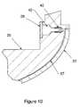
- FIG. 10shows a close up cross sectional view of an embodiment of the upper flow guide.
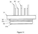
- FIG. 11shows a side view of an embodiment of the adjustable proportional flow injector assembly.
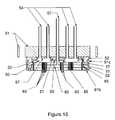
- FIG. 12shows an exploded side view of an embodiment of the adjustable proportional flow injector assembly.
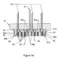
- FIGS. 13-15show three cross-sectional views of an embodiment of the adjustable proportional flow injector assembly.
- FIG. 16A-Bshows a top interior view of an embodiment of the adjustable proportional flow injector gas chamber machining.
- FIG. 17A-Bshows a bottom view of an embodiment of the adjustable proportional flow injector assembly
- FIG. 18shows a close up cross-sectional view of the dual o-ring seal of the adjustable proportional flow injector assembly sealed to a flow flange assembly.
- FIG. 19shows a perspective view of an embodiment of the chamber assembly.
- FIG. 20shows a top view of an embodiment of the chamber assembly.
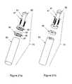
- FIGS. 21 a and 21 bshow two exploded views of an embodiment of the center rotation shaft assembly.
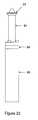
- FIG. 22shows a side view of an embodiment of the center rotation shaft assembly.
- FIG. 23shows a cross-sectional view of an embodiment of the center rotation shaft assembly.
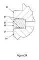
- FIG. 24shows a close up cross-sectional view of an embodiment of the center rotation shaft assembly.
- FIG. 25 a - cshows an alternate embodiment of subassemblies of the gas chambers of the adjustable proportional flow injector assembly.
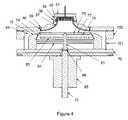
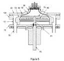
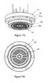
- FIG. 1illustrates a front perspective view of one embodiment of the entire reactor assembly 1 .
- the entire reactor assembly 1is comprised of three subassemblies that together form the entire reactor assembly 1 .
- the three subassembliesare the flow flange assembly 3 , the adjustable proportional flow injector assembly 5 , and the chamber assembly 7 .
- FIG. 2illustrates a side view of the reactor assembly 1 as well as some of the individual components that are visible from the exterior of the reactor 1 . Those components are discussed in more detail below.
- FIGS. 3-5illustrate a cross sectional view of the entire reactor assembly 1 showing the interconnection of the three subassemblies, and a cross-sectional view of the individual components that make up the three subassemblies.
- the flow flange assembly 3As in FIGS. 1 and 2 , the flow flange assembly 3 , the adjustable proportional flow injector assembly 5 and the chamber assembly 7 are illustrated.
- the individual components of the three subassemblies 3 , 5 , and 7are also indicated and discussed in greater detail below.
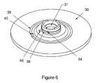
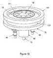
- FIGS. 6-10 and 18show several views of one embodiment of flow flange assembly 3 .
- the flow flange assembly 3comprises a main flange body 30 and has an upper opening 31 which defines a mating port for the flow injector assembly 5 on the top and mates to the chamber assembly 7 on the bottom end (shown best in the cross section view of FIGS. 3-5 .)
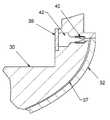
- the flow flange assembly 3has an upper flow guide 32 , which, along with the flow injector and wafer carrier, defines the reactor volume 33 and the gas flow profile within the reactor volume, fitted within the main flange body 30 .
- the upper flow guide 32preferably has a three-dimensional tapered cone outward facing surface 34 (as opposed to vertical cylindrical walls of prior art designs).
- the upper flow guide 32is positioned and fits within the main flange body 30 (as best shown in FIGS. 7 and 8 .
- the underside 35 of the main flange body 30has a corresponding shape to receive the inward facing surface 36 of the upper flow guide 32 so that a thin fluid gap or cavity 37 is formed immediately behind the upper flow guide 32 , between the upper flow guide 32 and the main flange body 30 (best illustrated in FIGS. 8-10 ).
- fluid cavity collection channels 41 , 42two points here connect with the thin fluid cavity 37 through flow orifices 40 .
- the geometry of the upper flow guide 32minimizes reactor chamber volume, suppresses recirculation eddies within the reactor chamber volume 33 and provides for efficient contacting of the reactant gas with the wafer carrier surface 77 .
- the upper flow guide 32has a first (upper) diameter D- 1 substantially equal to the diameter of the adjustable proportional flow injector (APFI) 7 and second (lower) diameter D- 2 substantially equal to the diameter d 3 of the wafer carrier 76 (as shown in FIG. 20 ).
- the first diameter D- 1is smaller than the second diameter D- 2 .
- the first diameter D- 1preferably is from about 0.2 to 0.5 of the second diameter D- 2 .
- the upper flow guide 32is not strictly conical shaped, but rather curved as the guide extends downward and flares out as it approaches D- 2 .
- the upper flow guide 32creates a gas flow pattern where a uniformly distributed, downward-flowing gas stream is directed towards the wafer carrier 76 , but the gas stream is also turned laterally and expanded, so that a smaller diameter flow injector 5 can be used to uniformly distribute flow over a substantially larger wafer carrier 76 , without the occurrence of recirculation of gas within the reactor chamber volume 33 .
- the curved or flared profile of the upper flow guide 32provides approximately equal radial gas velocity.
- An upper flow guide 32 with this geometryis alternately referred as an expanding cone upper flow guide 32 .
- the gasmust cross a continuously increasing cross sectional area (which increases with radius for cylindrical geometries), and as a result, the flow velocity must decrease.
- the height H- 1 of the containing geometrymay be gradually reduced, so that the cross sectional area (product of circumference multiplied by height) remains substantially constant, which counteracts the increase of the circumference with radius.
- the flow flange assembly 3preferably has a fluid gap 37 positioned directly behind the upper flow guide 32 (between the upper flow guide 32 and the main flange body 30 ).
- the fluid gap 37is relatively thin (about 0.1 inches or less) which, for fluid flow rates of approximately 1 gallon per minute and for fluids having density and viscosity values within an order of magnitude of water, will result in a Reynold's number value of less than 3200, which is indicative of laminar flow within the fluid gap and efficient usage of fluid. This configuration results in reduced usage of fluid and/or reduces the capacity of a fluid recirculator (if a reservoir/recirculator heat exchanger system is to be employed).
- the flow flange assembly 3may further comprise bottom/outer to top/inner flow through the fluid gap 37 for air removal and counter-flow heat exchange. That is, fluid flows in a reverse direction through the fluid gap from the direction the gas is flowing in the reactor volume.
- This type of flow path through the fluid gapis achieved in one embodiment from a supply channel 41 , optionally down through one or more supply conduits (not shown).
- Each supply channel 41has one or more flow restricting orifices 40 proximate to the end of each supply channel 41 .
- the flow restrictive orifices 40sufficiently restrict the flow such that an equal flow rate of fluid passes through each supply channel, immediately prior to entering the fluid gap 37 , producing a uniform flow delivery around the outer circumference of the fluid gap 37 .
- Fluidflows radially inward though the fluid gap 37 , and then passes through a second set of flow restricting orifices 40 within that transfers the fluid to a return channel 42 (optionally via one or more return conduits (not shown). Fluid is supplied via supply channel inlet tube 45 and returned through a fluid outlet tube 46 .
- the flow characteristics of the fluid within the fluid gap 37result in improved temperature uniformity within the reactor chamber volume 33 , which improves the uniformity of the gas flow profile and deposition uniformity.
- the bottom/outer to top/inner flow pattern in the fluid gap 37results in counter-flow heat exchange and effective removal of air from the gap 37 .
- a gap 43 between upper flow guide 32 at the outermost diameter of the upper flow guide D- 2 (i.e. at the end of the upper flow guide proximate to the wafer carrier 76 ) and wafer carrier upper surface 77 at the outermost diameter d 3 of the wafer carrier 76generally inhibits or prevents recirculation of ejected gas above the wafer carrier 76 .
- the wafer carrier 76rests on the top of a center rotation shaft 75 .
- the upper flow guide 32 outer diameter D- 2is about equal to that of the wafer carrier d 3 where the upper flow guide 32 is closest to the wafer carrier 76 .
- the gap 43facilitates the inhibition or prohibition of recirculation of the ejected gas within the reactor chamber volume 33 .
- the gapmay have a dimension H- 2 of about 1.00 inch or less, such as about 0.25 inch or less.
- the gas flowing downward from the adjustable proportional flow injector assembly 5turns laterally within the reactor chamber volume 33 and flows radially outward. When it reaches the gap 43 , the gas achieves a maximum flow velocity, and once past the gap 43 , the gas begins to expand and decelerate in an exhaust collection zone 44 that is proximate to the gap 43 , thereby preventing backward recirculation of the spent gas mixture, (i.e. the gas which has moved away from the reaction area at and above the wafer carrier 76 ).
- the reactor 1 with an expanding cone upper flow guide 32also incorporates a lower flow guide 72 (discussed in more detail below).
- the lower flow guide 72prevents gas recirculation back into the reaction zone, improves smoothness of flow from outer edge of wafer carrier into exhaust ports for more stable overall reactor flow profile, and reduces heat losses at outer edge of wafer carrier 76 for better temperature uniformity and improved material characteristics.
- the adjustable proportional flow injector assembly 5(hereinafter “APFI 5 ”) in an embodiment of the invention is shown particularly in FIGS. 11-18 and 25 .
- the adjustable proportional flow injectionis a flow injector that receives multiple gas inlet streams from supply tubes and spreads or diffuses these flows for a uniform outlet flow velocity, while keeping the gas streams separated until they exit.
- the APFI 5also regulates the temperature of the gases as they exit the adjustable proportional flow injector.
- the APFI 5is typically cylindrical in shape (circular area and vertical height) and fits within the flow flange assembly 3 .
- a cylindrical APFIis shown in the figures however, the APFI can be made in any shape and the exact shape will generally be dictated by the shape (area) of the upper opening 31 into which it is being mated. For example, if the upper opening 31 has a square or rectangular shape, then the APFI will have a corresponding square or rectangular shape so that it can be mated.
- the adjustable proportional flow injector assembly 5generally comprises a support flange 51 , which provides structural integrity for the components mated to the support flange 51 and gas chamber inlet tubes or ports 54 that penetrate through the support flange 51 .
- the support flange 51further provides for mating the entire adjustable proportional flow injector assembly 5 to a main flange body 30 .
- the APFI 5includes one or more gas chambers 52 .
- one or more of the gas chambers 50may be machined into a gas chamber machining 52 and are formed from a plurality of gas chamber top walls or surface 57 and gas chamber bottom walls or surface 58 .
- the gas chamber top wall 57can be machined to form different zones as illustrated in the top views FIGS. 16 and 17 .
- the gas chambers 50are separated from the other gas chambers 50 by gas chamber vertical walls 59 that extend from the gas chamber top walls 57 to the gas chamber bottom walls 58 thereby forming the gas chambers 50 .
- the one or more gas inlets 54which may be incorporated into the gas chamber top walls 57 , deliver gas to the one or more gas chambers 50 of the adjustable proportional flow injector 5 , such as in a vertical direction (i.e. about perpendicular to the gas chamber top walls 57 and gas chamber bottom walls 58 ).
- Each gas chamber 50may receive a different gas stream and one or more of these gas chambers may spread or diffuse the gas and keep a first gas stream separate from other gas streams or each gas stream separate from another, and create a uniform flow velocity over a specific outlet surface area. Additionally, each gas chamber 50 may be configured in the same shape or different shape as the other gas chambers 50 .
- the support flange 51is removed from the figure
- there is an outer gas chamber 50 aand four intermediate gas chambers 50 b and 50 c , and an inner gas chamber 50 d .
- the gas chamber 50 breceives Group III reactants and intermediate gas chambers 50 c receive group V reactants.
- the chambers 50 a - dare separated by the vertical walls 59 , the gas chamber top walls 57 (not shown) and the gas chamber bottom walls 58 .
- the APFI 5may also include a fluid cavity 60 , which is located below the one or more gas chambers 50 .
- the fluid cavity 60may be formed by the mating of a fluid cavity machining 53 to the gas chamber machining 52 .
- FIG. 17shows the bottom view of an embodiment of the adjustable proportional flow injector assembly 5 , showing the bottom face of the fluid cavity machining 53 .
- Gas chamber outlets 61may extend or penetrate from the bottom wall 58 of a gas chamber through the fluid cavity 60 , such as through conduit tubes 63 , into the reactor chamber volume 33 .
- the conduit tubes 63may have the same or different inner diameters and same or different outer diameters.
- the fluid cavity 60has a fluid cavity outlet 66 positioned at about the center of the fluid cavity 60 connected to a fluid cavity outlet tube 67 . Additionally, fluid cavity inlets 68 are provided through fluid cavity inlet tubes 69 towards the periphery of the fluid cavity 60 .
- the fluid cavity outlet 68is positioned inside the circumference of the diffuser 65 , while the fluid cavity inlets 68 are positioned outside of the circumference of the diffuser 65 .
- the adjustable proportional flow injector assembly 5may optionally have one or more of the following features.
- the gas outlet apertures 61are preferably a smaller size than the gas inlets 54 (for example there may be from about 100 to about 10,000 gas outlet apertures).
- the number of gas outlet apertures 61 and the inside diameter and length of the conduit tubes 63 extending through the fluid cavity 60depends on the specific gas composition, flowrate, temperature and pressure and are also limited by the total surface area of the bottom wall 58 of a gas chamber and by manufacturing capabilities and costs, the difficulty and cost increasing as the outside and inside diameters of the conduit tubes 63 decreases and as the spacing of adjacent gas outlet apertures 61 decreases.
- the total cross sectional area of all of the conduit tubes 63is preferably a factor between 2 and 6 times larger than the cross sectional area of the gas inlet 54 to a given gas chamber.
- This arrangementaccounts for the greater wall surface area and corresponding fluid shear and pressure drop of the smaller-diameter conduit tubes 63 compared to the gas inlet 54 , such that the pressure drop across the set of conduit tubes of a given gas chamber (that is, the pressure drop from the gas chamber to the reactor chamber volume 33 ) is preferably from several Torr to several tens of Torr.
- the gas chamber upper walls 57 and gas chamber bottom wallsmay preferably be substantially parallel.
- the upper walls/surface 57 of all gas chamberscan be substantially co-planar they can alternatively be on different planes.
- gas chamber bottom walls 58 of all gas chambers 50can be co-planar or alternatively on different planes.
- the adjustable proportional flow injector assembly 5may optionally comprise one or more intermediate diffusing baffle plates 55 between and substantially parallel to the gas chamber upper walls 57 and the gas chamber bottom walls 58 .
- an intermediate diffusing baffle plate 55When an intermediate diffusing baffle plate 55 is used, an upper gas chamber section 50 a and a lower gas chamber section 50 b is formed in the gas chamber 50 comprising the intermediate diffusing baffle plates 55 .
- the upper gas chamber section 50 amay be defined, generally, by the gas chamber upper wall 57 , an upper surface of the intermediate diffusing baffle plate 55 and any side wall(s) 59 and the lower gas chamber section 50 b may be defined generally by the gas chamber lower wall 58 , a lower surface of the intermediate diffusing baffle plate 55 and any side wall(s) 59 .
- Gas outlet apertures 61 of each gas chamber 50are joined to outlet conduits (preferably small diameter tubes) 63 penetrating through the fluid cavity 60 which may be attached to or otherwise joined to the fluid cavity machining 53 thereby forming a lower fluid cavity wall proximate to the lowermost side of which is a boundary surface of the reactor chamber volume 33 .
- the outlet conduits 63preferably have an aperture pattern matching that of the combined set of gas chamber outlet apertures 61 .
- a further embodiment of the adjustable proportional flow injector assembly 5concerns a fluid temperature control zone with uniform, radial flow profile. Temperature regulating fluid, for example cooling fluid, flows into an outer distribution channel 62 .
- the fluid cavity 60has a fluid cavity diffuser 65 .
- the fluid cavity diffuser 65is preferably a thin, cylindrical sheet metal ring having a height slightly larger than the height of the fluid cavity 60 and is preferably as thin as possible.
- the cylindrical sheet metal ringinserts into opposing circular grooves in the bottom surface of the gas chamber machining 53 and the upper surface of the fluid cavity machining 52 , the sum of the depth of these two grooves preferably being equal to the additional height of the flow diffusing barrier over that of the fluid cavity, so that fluid delivered to the fluid cavity 60 at multiple inlets 68 at the outermost periphery of the fluid cavity must immediately move tangentially before flowing through a plurality of preferably equally spaced small apertures 64 in the flow diffusing barrier 65 , resulting in a uniform flow distribution from the outermost periphery of the fluid cavity 60 radially inward towards the single outlet 66 at the center outlet 66 of the fluid cavity 60 .
- the small apertures 64act as flow restricting orifices, which sufficiently restrict flow so as to result in an equal flow through each aperture 64
- FIG. 25( a - c )illustrates an alternate method of fabricating the APFI. Not all APFI components previously described are shown.
- components of the APFIcan be assembled from interchangeable modules or subassemblies.
- gas outlet aperture sub-assemblies 150can be constructed from an upper plate 151 , a lower plate 152 , and multiple conduits 63 .
- the upper plate 151constitutes the bottom wall 58 of a gas chamber 50 described above.
- the lower plate 152constitutes a portion of the bottom wall 58 of the fluid cavity machining 53 previously described.
- the gas chamber machining 52is constructed to receive multiple gas outlet aperture sub-assemblies 150 , such that the upper surface 153 of the upper plate 151 mates flush to one or more lower surfaces 155 of gas chamber walls 59 previously described.
- the seam between the upper plates 151 of adjacent gas outlet aperture sub-assemblies 150falls along the centerline of a given lower surface 155 of a gas chamber wall 59 so that a seal may be formed that prevents any leakage between the fluid cavity 63 thus formed and any gas chamber 50 .
- the seam between the lower plates 152 of adjacent gas outlet aperture sub-assemblies 150 and between the lower plate 152 of a given gas outlet aperture sub-assembly 150 and the lower fluid cavity wall 157 integral with that gas chamber machining 52may be sealed to prevent any leakage between the fluid cavity 63 and the reactor chamber volume 33 .
- itmay be sealed in such a manner that the lower surface 154 of each gas outlet aperture sub-assembly 150 is flush with the lower surface 154 of all other gas outlet aperture sub-assemblies 150 and the lower surface 156 of the gas chamber machining, although this is not required.
- Fluidis thus delivered into the fluid cavity 63 through multiple fluid cavity inlets 68 and exits through one or more fluid cavity outlets 66 , where the fluid cavity diffuser 65 (not shown) is positioned in a similar manner as previously described.
- a further embodiment of the inventionconcerns methods for creating patterns of substantially equally spaced gas outlets in one or more radial patterns.
- one or more patterns of circular holesare arranged such that the holes are equidistant from each other, such as in square or hexagonal patterns.
- a methodcomprises distributing holes so that they are substantially equidistant from each other as well as area boundaries.
- This methodgenerally comprises the steps of (1) arranging a first set of holes on a first line adjacent and parallel to a first radial area boundary, with equal spacing between these holes in a radial direction, (2) determining the angle, with vertex at the center axis of the machining, between a first point on the first line at a first radial distance from the center axis and the corresponding second point on a second line adjacent and parallel to a second radial area boundary, (3) determining the length of the arc, with origin at the center of the gas chamber machining, between a first hole at a given radius lying adjacent to the first radial area boundary and the corresponding second hole at the same radius lying adjacent to the second corresponding radial area boundary, (4) dividing this arc length by the desired center-to-center hole spacing distance and (5) rounding the resulting number to the nearest integer.
- Steps (2)-(5)are repeated for each hole comprising the set described in step (1).
- This methodproduces a hole pattern with equal separation between radial sets of holes, and nearly equal separation of holes within each radial set of holes.
- This methodis particularly useful for producing substantially equidistant sets of holes in circular or semi-circular patterns over small areas, where irregularities in hole spacing are more significant than for patterns over large areas.
- the reactorsmay also comprise a gas distribution zone having adjustability with no zone separating barriers (such as illustrated in FIG. 17 ).
- the reactorscomprise two or more gas inlet tubes 54 and a plurality of outlet holes 61 that geometrically function to produce an adjustable outlet flow pattern through the plurality of holes 61 . While not bound by theory, by increasing or decreasing the amount flow to one or more of the inlet tubes 54 , without having any discrete vertical separation wall 59 between any of the inlet tubes 54 , stagnation areas that would normally be produced by the area below the separation walls, which can have not outlet flow holes, are eliminated.
- the adjustable proportional flow injector assembly 5may further comprise one or more sealed chamber tops, such as one or more o-ring sealed chamber tops, for cleaning and/or baffle changes.
- the gas chamber machining 52includes o-ring grooves machined into the top surface of the vertical walls 59 separating the gas chambers, which eliminates the gas chamber zone upper walls 57 . This is because an o-ring lying along the upper surface of the vertical walls can seal directly to the lower surface of the support flange 51 or other single intermediate sealing surface (rather than a plurality of welded surfaces). This configuration allows the gas chambers to be opened and cleaned or inspected, as well as reducing the number of parts required.
- the adjustable proportional flow injector assembly 5comprises a dual o-ring seal with vacuum barrier zone, best illustrated in FIG. 18 .
- Dual o-ring sealproduced by o-rings 91 in o-ring grooves 92 in the gas chamber machining 52 and the fluid cavity machining 53 .
- One o-ring 91 ais positioned between the gas chamber machining 52 and the main flange body 31 .
- a second 91 bis positioned between the fluid cavity machining 53 and the main flange body 30 .
- a vacuum cavity 93is created between the APFI, the main flange body 31 , and the o-rings 91 .
- a differential seal vacuum port tube 94is included in the main flange body 31 to create and release the vacuum seal.
- This configurationpermits easy removal of the adjustable proportional flow injector 5 while negating gas molecule permeation of the o-ring elastomer material, due to the significantly lower vacuum levels produced in the volume in between the two o-ring seals than on either side of each seal.
- the chamber assembly 7has a reactor baseplate main body 70 .
- the reactor baseplate main bodyis connected to a reactor jar top flange 100 via a reactor jar wall 101 .
- the reactor jar top flange 100mates with the main flange body 30 of the flow flange assembly 3 .
- the baseplate main body 70contains ports for a number of components useful in CVD reactors such as a center rotation shaft 75 (discussed in more detail below), base plate exhaust tubes 79 ; high current feedthrough 90 ; and rotary vacuum feedthrough housing 88 .
- the chamber assembly 7has components typically found in a CVD reactor such as a heater assembly comprising a heat source and heat reflecting shields for heating the wafer carrier 76 .
- a heater assemblycomprising a heat source and heat reflecting shields for heating the wafer carrier 76 .
- one or more heating elements 83are positioned under the wafer carrier 76 and one or more heat shields 84 are positioned under the heating elements 83 .
- the heat sourcemay be a filament for radiant heating or a copper tube for inductive heating, preferably arranged in a concentric circular pattern to match the circular area of the wafer carrier.
- Other types of heater assembliesmay be used for heating the wafer carrier 76 .
- the chamber assembly 7has a lower flow guide 72 .
- the lower flow guide 72has a frustoconical shape.
- the conical shaped lower flow guide 74has an inner diameter d- 1 and an outer diameter d- 2 .
- the inner diameter d- 1is slightly larger than outer diameter d 3 of the wafer carrier 76 , although the inner diameter d- 1 can be approximately the same, smaller or larger than the outer diameter d 3 of the wafer carrier 76 .
- the lower flow guide 72is aligned approximately with the top surface 77 of wafer carrier 76 .
- the outer diameter d- 2 of the lower flow guide 72is larger than the inner diameter d- 1 creating a sloping surface in the downward direction.
- the inner diameter d- 1is slightly larger than outer diameter d 3 of the wafer carrier 76 .
- the spacing between the inner diameter d- 1 of the lower flow guide 72 and the outer diameter of the wafer carrier 76forces the gas ejected from the gap 43 between the wafer carrier 76 and the upper flow guide 32 to expand gradually, and inhibits or prevents recirculation of the ejected gas below the outer edge of the wafer carrier 76 .
- the inner diameter d- 1 of the lower flow guide and the outer diameter of the wafer carrier 76are in close proximity to provide a narrow lower flow guide gap between the two, as the narrower the lower flow guide gap the more efficient ejection of the gas and greater the inhibition or prevention of the recirculation of gases within the reactor chamber volume 33 .
- the lower flow guide 72is fabricated from graphite.
- the chamber assembly 7may contain a lower flow guide reflector 74 .
- the lower flow guide reflector 74is positioned within the lower flow guide 72 and extending from the circumference of the wafer carrier 76 and angled in a downward direction.
- the reflector 74is constructed of a thin piece of metal, preferably molybdenum. The reflector 74 acts to reflects heat inward and helps keep the heat constant over the surface of the lower flow guide 72 .
- the lower flow guide 72may be constructed of one or more sections or pieces, such as a two-piece lower flow guide 72 . Due to the close spacing between the lower flow guide 72 and the wafer carrier 76 , and due to the high temperature the wafer carrier 76 reaches during processing, in an alternate embodiment, the lower flow guide 76 has a first piece that is immediately adjacent to the wafer carrier 76 fabricated from a material having a superior temperature tolerance and coefficient of thermal expansion about equal to or similar to that of the wafer carrier 76 material (typically graphite, sapphire or a refractory metal), and a second piece fabricated from a material that does not have such temperature tolerance or coefficient of thermal expansion, such as a material that is less expensive and more easily formed than the material that comprises the first piece.
- the first pieceis fabricated from graphite to provide the appropriate temperature tolerance and coefficient of thermal expansion match with the wafer carrier material.
- the lower flow guide 72may be in part or wholly an extension of the wafer carrier 76 extending from the diameter d 3 of the surface of the wafer carrier 76 that holds the wafer, i.e. an outer edge profile of the wafer carrier surface 77 that holds the wafers.
- all or a portion of the lower flow guide 76is an extension of the wafer carrier from the outer circumference of preferably the wafer carrier top surface 77 , or alternatively the lower surface 78 , or at some point along the circumference in between.
- the lower flow guide 72has a first section which is an extension of the wafer carrier 76 , such as within the first few centimeters from the narrow gap 40 between the wafer carrier outer diameter 76 and the upper flow guide 72 , and a second piece that is completely separate from the wafer carrier 76 and is formed as a separate piece adjacent to the first piece.
- the wafer carrier 76 for the reactor 1may be a conventional one piece structure, however, embodiments having alternative structures are within the scope of the invention.
- the reactormay comprise a two-piece wafer carrier 76 comprising a removable top (i.e. platter or surface that holds the wafers) and a bottom.
- the removable topmay be made from a number of materials, preferably sapphire and bottom may comprise graphite and may further comprise a means for heating, such as RF heated (for inductive heating of bottom and conductive heating of removable top and any wafers on the surface of the removable top).
- the two-piece wafer carriercan have the removable top replaced when necessary while the bottom can be reused.
- a two-piece wafer carrierhas a sapphire removable top for holding the wafers and a graphite bottom that supports the sapphire removable top.
- the sapphire topis non-porous and will not degrade, which occurs with surfaces conventionally used, such as SiC encapsulant.
- the sapphire removable topcan also be cleaned more rigorously (such as a rapid wet chemical etch, which is not easily performed with the graphite wafer carriers).
- the graphite bottom pieceis a heat absorber for conductive heat transfer into the sapphire removable top and the wafers on the surface of the removable top, such as within wafer pockets that may be machined in an upper surface of the removable top.
- the wafer carrier 76is integral with (i.e. machined directly into) a portion of the center rotation shaft 75 , which shaft 75 extends downward from the center of a bottom surface 78 of the wafer carrier 76 .
- the center shaft 75(alternatively, the center rotation shaft 75 ) extends downward through a heating coil and is comprised of a material suitable for heating, for example a material suitable for induction heating. This center rotation 75 shaft can be heated just as the main portion of the wafer carrier 76 is, and provides a thermal barrier to the conductive heat losses that may occur with conventional supporting spindle shafts.
- the center rotation shaft 75 for the wafer carrier 76may be a conventional one piece structure; however, embodiments having alternative structures may be used.
- a multi-segment shaft 75 for the rotating wafer carrieri.e. a shaft comprising one or more segments made from the same material or different material is used.
- at least one segmentwill have a substantially lower thermal conductivity than the remaining shaft segment(s) used.
- the multi-segment spindleis particularly useful in conjunction with radiant heaters although the invention is not necessarily limited in this regard.
- a shaft upper segment 81is directly in contact with the wafer carrier 76 .
- the shaft upper segment 81has a susceptor or flange 82 at the proximal end on which the bottom surface 78 of the wafer carrier 76 rests.
- the upper segmentis preferably fabricated from a material (such as alumina or sapphire) having a lower thermal conductivity than the one or more of the remaining segment(s) of the multi-segment shaft 75 . This selection of material produces the highest possible thermal transfer resistance.
- Segment interfaces between the multi-segment center shaft 75 and the wafer carrier 76can be designed with minimal surface to further enhance the thermal transfer resistance. These features improve the temperature uniformity near the center area of the wafer carrier, as well as reduce energy losses in operation of the reactor.
- the segment in contact with the wafer carrierextends downward through an inductive heating coil.
- the upper segment 81is made of a material suitable for inductive heating.
- the upper segment 81 of the multi-segment center shaft 75is preferably constructed of graphite.
- the multi-segment shaft 75has a shaft lower segment 85 is constructed of a material that does not readily heat inductively (such as sapphire).
- the shaft upper segment 81 and shaft lower segment 85are connected via a spacer 86 that is, preferably, constructed from alumina.
- the interfaces between the three (or more) segmentspreferably have minimal surface contact area to produce the highest possible thermal transfer resistance.
- the surface areamay be reduced by including machined recesses 87 in the segments at the point of interface (shown in FIG. 24 ); to create thin rails 96 around the circumference of the ends of the segments. Contact between the segments only occurs at the thin rails 96 as opposed to the entire area of the segment ends.
- the segmentsare preferably secured by way of vented head cap screws 97 .
Landscapes
- Chemical & Material Sciences (AREA)
- Engineering & Computer Science (AREA)
- General Chemical & Material Sciences (AREA)
- Chemical Kinetics & Catalysis (AREA)
- Materials Engineering (AREA)
- Mechanical Engineering (AREA)
- Metallurgy (AREA)
- Organic Chemistry (AREA)
- Physics & Mathematics (AREA)
- Condensed Matter Physics & Semiconductors (AREA)
- General Physics & Mathematics (AREA)
- Manufacturing & Machinery (AREA)
- Computer Hardware Design (AREA)
- Microelectronics & Electronic Packaging (AREA)
- Power Engineering (AREA)
- Chemical Vapour Deposition (AREA)
Abstract
Description
Claims (19)
Priority Applications (3)
| Application Number | Priority Date | Filing Date | Title |
|---|---|---|---|
| US12/248,167US8778079B2 (en) | 2007-10-11 | 2008-10-09 | Chemical vapor deposition reactor |
| US14/186,102US20140216347A1 (en) | 2007-10-11 | 2014-02-21 | Chemical vapor deposition reactor |
| US14/186,089US20140216341A1 (en) | 2007-10-11 | 2014-02-21 | Chemical vapor deposition reactor |
Applications Claiming Priority (2)
| Application Number | Priority Date | Filing Date | Title |
|---|---|---|---|
| US97918107P | 2007-10-11 | 2007-10-11 | |
| US12/248,167US8778079B2 (en) | 2007-10-11 | 2008-10-09 | Chemical vapor deposition reactor |
Related Child Applications (2)
| Application Number | Title | Priority Date | Filing Date |
|---|---|---|---|
| US14/186,089DivisionUS20140216341A1 (en) | 2007-10-11 | 2014-02-21 | Chemical vapor deposition reactor |
| US14/186,102DivisionUS20140216347A1 (en) | 2007-10-11 | 2014-02-21 | Chemical vapor deposition reactor |
Publications (2)
| Publication Number | Publication Date |
|---|---|
| US20120111271A1 US20120111271A1 (en) | 2012-05-10 |
| US8778079B2true US8778079B2 (en) | 2014-07-15 |
Family
ID=40549831
Family Applications (3)
| Application Number | Title | Priority Date | Filing Date |
|---|---|---|---|
| US12/248,167Expired - Fee RelatedUS8778079B2 (en) | 2007-10-11 | 2008-10-09 | Chemical vapor deposition reactor |
| US14/186,102AbandonedUS20140216347A1 (en) | 2007-10-11 | 2014-02-21 | Chemical vapor deposition reactor |
| US14/186,089AbandonedUS20140216341A1 (en) | 2007-10-11 | 2014-02-21 | Chemical vapor deposition reactor |
Family Applications After (2)
| Application Number | Title | Priority Date | Filing Date |
|---|---|---|---|
| US14/186,102AbandonedUS20140216347A1 (en) | 2007-10-11 | 2014-02-21 | Chemical vapor deposition reactor |
| US14/186,089AbandonedUS20140216341A1 (en) | 2007-10-11 | 2014-02-21 | Chemical vapor deposition reactor |
Country Status (6)
| Country | Link |
|---|---|
| US (3) | US8778079B2 (en) |
| EP (1) | EP2215282B1 (en) |
| JP (1) | JP2011500961A (en) |
| KR (1) | KR101177983B1 (en) |
| CN (1) | CN101802254B (en) |
| WO (1) | WO2009049020A2 (en) |
Cited By (149)
| Publication number | Priority date | Publication date | Assignee | Title |
|---|---|---|---|---|
| US20110277690A1 (en)* | 2010-05-14 | 2011-11-17 | Sierra Solar Power, Inc. | Multi-channel gas-delivery system |
| US20120152171A1 (en)* | 2009-08-31 | 2012-06-21 | Wonik Ips Co., Ltd. | Gas injection apparatus and substrate processing apparatus using same |
| US20130206338A1 (en)* | 2012-01-20 | 2013-08-15 | Tokyo Electron Limited | Plasma processing apparatus |
| US20140097270A1 (en)* | 2012-09-21 | 2014-04-10 | Applied Materials, Inc. | Chemical control features in wafer process equipment |
| US20150187629A1 (en)* | 2013-12-31 | 2015-07-02 | Lam Research Ag | Apparatus for treating surfaces of wafer-shaped articles |
| US20150187624A1 (en)* | 2013-12-31 | 2015-07-02 | Lam Research Ag | Apparatus for treating surfaces of wafer-shaped articles |
| US20150361581A1 (en)* | 2013-03-12 | 2015-12-17 | Applied Materials, Inc. | Window assembly for substrate processing system |
| US9269590B2 (en) | 2014-04-07 | 2016-02-23 | Applied Materials, Inc. | Spacer formation |
| US9287134B2 (en) | 2014-01-17 | 2016-03-15 | Applied Materials, Inc. | Titanium oxide etch |
| US9287095B2 (en) | 2013-12-17 | 2016-03-15 | Applied Materials, Inc. | Semiconductor system assemblies and methods of operation |
| US9293568B2 (en) | 2014-01-27 | 2016-03-22 | Applied Materials, Inc. | Method of fin patterning |
| US9299575B2 (en) | 2014-03-17 | 2016-03-29 | Applied Materials, Inc. | Gas-phase tungsten etch |
| US9299538B2 (en) | 2014-03-20 | 2016-03-29 | Applied Materials, Inc. | Radial waveguide systems and methods for post-match control of microwaves |
| US9299583B1 (en) | 2014-12-05 | 2016-03-29 | Applied Materials, Inc. | Aluminum oxide selective etch |
| US9299537B2 (en) | 2014-03-20 | 2016-03-29 | Applied Materials, Inc. | Radial waveguide systems and methods for post-match control of microwaves |
| US9309598B2 (en) | 2014-05-28 | 2016-04-12 | Applied Materials, Inc. | Oxide and metal removal |
| US9324576B2 (en) | 2010-05-27 | 2016-04-26 | Applied Materials, Inc. | Selective etch for silicon films |
| US9343272B1 (en) | 2015-01-08 | 2016-05-17 | Applied Materials, Inc. | Self-aligned process |
| US9349605B1 (en) | 2015-08-07 | 2016-05-24 | Applied Materials, Inc. | Oxide etch selectivity systems and methods |
| US9355863B2 (en) | 2012-12-18 | 2016-05-31 | Applied Materials, Inc. | Non-local plasma oxide etch |
| US9355856B2 (en) | 2014-09-12 | 2016-05-31 | Applied Materials, Inc. | V trench dry etch |
| US9355862B2 (en) | 2014-09-24 | 2016-05-31 | Applied Materials, Inc. | Fluorine-based hardmask removal |
| US9368364B2 (en) | 2014-09-24 | 2016-06-14 | Applied Materials, Inc. | Silicon etch process with tunable selectivity to SiO2 and other materials |
| US9373522B1 (en) | 2015-01-22 | 2016-06-21 | Applied Mateials, Inc. | Titanium nitride removal |
| US9373517B2 (en) | 2012-08-02 | 2016-06-21 | Applied Materials, Inc. | Semiconductor processing with DC assisted RF power for improved control |
| US9378978B2 (en) | 2014-07-31 | 2016-06-28 | Applied Materials, Inc. | Integrated oxide recess and floating gate fin trimming |
| US9378969B2 (en) | 2014-06-19 | 2016-06-28 | Applied Materials, Inc. | Low temperature gas-phase carbon removal |
| US9385028B2 (en) | 2014-02-03 | 2016-07-05 | Applied Materials, Inc. | Air gap process |
| US9384997B2 (en) | 2012-11-20 | 2016-07-05 | Applied Materials, Inc. | Dry-etch selectivity |
| US9390937B2 (en) | 2012-09-20 | 2016-07-12 | Applied Materials, Inc. | Silicon-carbon-nitride selective etch |
| US9396989B2 (en) | 2014-01-27 | 2016-07-19 | Applied Materials, Inc. | Air gaps between copper lines |
| US9406523B2 (en) | 2014-06-19 | 2016-08-02 | Applied Materials, Inc. | Highly selective doped oxide removal method |
| US9412608B2 (en) | 2012-11-30 | 2016-08-09 | Applied Materials, Inc. | Dry-etch for selective tungsten removal |
| US9418858B2 (en) | 2011-10-07 | 2016-08-16 | Applied Materials, Inc. | Selective etch of silicon by way of metastable hydrogen termination |
| US9425058B2 (en) | 2014-07-24 | 2016-08-23 | Applied Materials, Inc. | Simplified litho-etch-litho-etch process |
| US20160244876A1 (en)* | 2013-02-23 | 2016-08-25 | Hermes-Epitek Corporation | Gas injector and cover plate assembly for semiconductor equipment |
| US9437451B2 (en) | 2012-09-18 | 2016-09-06 | Applied Materials, Inc. | Radical-component oxide etch |
| US9449846B2 (en) | 2015-01-28 | 2016-09-20 | Applied Materials, Inc. | Vertical gate separation |
| US9449845B2 (en) | 2012-12-21 | 2016-09-20 | Applied Materials, Inc. | Selective titanium nitride etching |
| US9449850B2 (en) | 2013-03-15 | 2016-09-20 | Applied Materials, Inc. | Processing systems and methods for halide scavenging |
| US9449859B2 (en)* | 2009-10-09 | 2016-09-20 | Applied Materials, Inc. | Multi-gas centrally cooled showerhead design |
| US9472417B2 (en) | 2013-11-12 | 2016-10-18 | Applied Materials, Inc. | Plasma-free metal etch |
| US9472412B2 (en) | 2013-12-02 | 2016-10-18 | Applied Materials, Inc. | Procedure for etch rate consistency |
| US9478432B2 (en) | 2014-09-25 | 2016-10-25 | Applied Materials, Inc. | Silicon oxide selective removal |
| US9487863B2 (en)* | 2015-02-06 | 2016-11-08 | Hitachi Kokusai Electric Inc. | Substrate processing apparatus |
| US9493879B2 (en) | 2013-07-12 | 2016-11-15 | Applied Materials, Inc. | Selective sputtering for pattern transfer |
| US9496167B2 (en) | 2014-07-31 | 2016-11-15 | Applied Materials, Inc. | Integrated bit-line airgap formation and gate stack post clean |
| US9502258B2 (en) | 2014-12-23 | 2016-11-22 | Applied Materials, Inc. | Anisotropic gap etch |
| US9499898B2 (en) | 2014-03-03 | 2016-11-22 | Applied Materials, Inc. | Layered thin film heater and method of fabrication |
| US9518321B2 (en) | 2014-07-31 | 2016-12-13 | Hitachi Kokusai Electric Inc. | Atomic layer deposition processing apparatus to reduce heat energy conduction |
| US9553102B2 (en) | 2014-08-19 | 2017-01-24 | Applied Materials, Inc. | Tungsten separation |
| US9576809B2 (en) | 2013-11-04 | 2017-02-21 | Applied Materials, Inc. | Etch suppression with germanium |
| US9607856B2 (en) | 2013-03-05 | 2017-03-28 | Applied Materials, Inc. | Selective titanium nitride removal |
| US9659753B2 (en) | 2014-08-07 | 2017-05-23 | Applied Materials, Inc. | Grooved insulator to reduce leakage current |
| US9691645B2 (en) | 2015-08-06 | 2017-06-27 | Applied Materials, Inc. | Bolted wafer chuck thermal management systems and methods for wafer processing systems |
| US9721789B1 (en) | 2016-10-04 | 2017-08-01 | Applied Materials, Inc. | Saving ion-damaged spacers |
| US9728437B2 (en) | 2015-02-03 | 2017-08-08 | Applied Materials, Inc. | High temperature chuck for plasma processing systems |
| US9741593B2 (en) | 2015-08-06 | 2017-08-22 | Applied Materials, Inc. | Thermal management systems and methods for wafer processing systems |
| US9748434B1 (en) | 2016-05-24 | 2017-08-29 | Tesla, Inc. | Systems, method and apparatus for curing conductive paste |
| US9768034B1 (en) | 2016-11-11 | 2017-09-19 | Applied Materials, Inc. | Removal methods for high aspect ratio structures |
| US9773648B2 (en) | 2013-08-30 | 2017-09-26 | Applied Materials, Inc. | Dual discharge modes operation for remote plasma |
| US9842744B2 (en) | 2011-03-14 | 2017-12-12 | Applied Materials, Inc. | Methods for etch of SiN films |
| US9865484B1 (en) | 2016-06-29 | 2018-01-09 | Applied Materials, Inc. | Selective etch using material modification and RF pulsing |
| US9881805B2 (en) | 2015-03-02 | 2018-01-30 | Applied Materials, Inc. | Silicon selective removal |
| US9885117B2 (en) | 2014-03-31 | 2018-02-06 | Applied Materials, Inc. | Conditioned semiconductor system parts |
| US9887096B2 (en) | 2012-09-17 | 2018-02-06 | Applied Materials, Inc. | Differential silicon oxide etch |
| US9934942B1 (en) | 2016-10-04 | 2018-04-03 | Applied Materials, Inc. | Chamber with flow-through source |
| US9947549B1 (en) | 2016-10-10 | 2018-04-17 | Applied Materials, Inc. | Cobalt-containing material removal |
| US9954136B2 (en) | 2016-08-03 | 2018-04-24 | Tesla, Inc. | Cassette optimized for an inline annealing system |
| US9972740B2 (en) | 2015-06-07 | 2018-05-15 | Tesla, Inc. | Chemical vapor deposition tool and process for fabrication of photovoltaic structures |
| US10008368B2 (en)* | 2013-03-12 | 2018-06-26 | Applied Materials, Inc. | Multi-zone gas injection assembly with azimuthal and radial distribution control |
| US10026621B2 (en) | 2016-11-14 | 2018-07-17 | Applied Materials, Inc. | SiN spacer profile patterning |
| US10043684B1 (en) | 2017-02-06 | 2018-08-07 | Applied Materials, Inc. | Self-limiting atomic thermal etching systems and methods |
| US10043674B1 (en) | 2017-08-04 | 2018-08-07 | Applied Materials, Inc. | Germanium etching systems and methods |
| US10049891B1 (en) | 2017-05-31 | 2018-08-14 | Applied Materials, Inc. | Selective in situ cobalt residue removal |
| US10062579B2 (en) | 2016-10-07 | 2018-08-28 | Applied Materials, Inc. | Selective SiN lateral recess |
| US10062585B2 (en) | 2016-10-04 | 2018-08-28 | Applied Materials, Inc. | Oxygen compatible plasma source |
| US10062578B2 (en) | 2011-03-14 | 2018-08-28 | Applied Materials, Inc. | Methods for etch of metal and metal-oxide films |
| US10062575B2 (en) | 2016-09-09 | 2018-08-28 | Applied Materials, Inc. | Poly directional etch by oxidation |
| US10062587B2 (en) | 2012-07-18 | 2018-08-28 | Applied Materials, Inc. | Pedestal with multi-zone temperature control and multiple purge capabilities |
| US10115856B2 (en) | 2016-10-31 | 2018-10-30 | Tesla, Inc. | System and method for curing conductive paste using induction heating |
| US10128086B1 (en) | 2017-10-24 | 2018-11-13 | Applied Materials, Inc. | Silicon pretreatment for nitride removal |
| US10163696B2 (en) | 2016-11-11 | 2018-12-25 | Applied Materials, Inc. | Selective cobalt removal for bottom up gapfill |
| US10170336B1 (en) | 2017-08-04 | 2019-01-01 | Applied Materials, Inc. | Methods for anisotropic control of selective silicon removal |
| US10224210B2 (en) | 2014-12-09 | 2019-03-05 | Applied Materials, Inc. | Plasma processing system with direct outlet toroidal plasma source |
| US10242908B2 (en) | 2016-11-14 | 2019-03-26 | Applied Materials, Inc. | Airgap formation with damage-free copper |
| US10256112B1 (en) | 2017-12-08 | 2019-04-09 | Applied Materials, Inc. | Selective tungsten removal |
| US10256079B2 (en) | 2013-02-08 | 2019-04-09 | Applied Materials, Inc. | Semiconductor processing systems having multiple plasma configurations |
| US10283324B1 (en) | 2017-10-24 | 2019-05-07 | Applied Materials, Inc. | Oxygen treatment for nitride etching |
| US10283321B2 (en) | 2011-01-18 | 2019-05-07 | Applied Materials, Inc. | Semiconductor processing system and methods using capacitively coupled plasma |
| US10297458B2 (en) | 2017-08-07 | 2019-05-21 | Applied Materials, Inc. | Process window widening using coated parts in plasma etch processes |
| US10319739B2 (en) | 2017-02-08 | 2019-06-11 | Applied Materials, Inc. | Accommodating imperfectly aligned memory holes |
| US10319600B1 (en) | 2018-03-12 | 2019-06-11 | Applied Materials, Inc. | Thermal silicon etch |
| US10319649B2 (en) | 2017-04-11 | 2019-06-11 | Applied Materials, Inc. | Optical emission spectroscopy (OES) for remote plasma monitoring |
| US10354889B2 (en) | 2017-07-17 | 2019-07-16 | Applied Materials, Inc. | Non-halogen etching of silicon-containing materials |
| US10403507B2 (en) | 2017-02-03 | 2019-09-03 | Applied Materials, Inc. | Shaped etch profile with oxidation |
| US10403474B2 (en)* | 2016-07-11 | 2019-09-03 | Lam Research Corporation | Collar, conical showerheads and/or top plates for reducing recirculation in a substrate processing system |
| US10407771B2 (en)* | 2014-10-06 | 2019-09-10 | Applied Materials, Inc. | Atomic layer deposition chamber with thermal lid |
| US10424485B2 (en) | 2013-03-01 | 2019-09-24 | Applied Materials, Inc. | Enhanced etching processes using remote plasma sources |
| US10431429B2 (en) | 2017-02-03 | 2019-10-01 | Applied Materials, Inc. | Systems and methods for radial and azimuthal control of plasma uniformity |
| US10468267B2 (en) | 2017-05-31 | 2019-11-05 | Applied Materials, Inc. | Water-free etching methods |
| US10490406B2 (en) | 2018-04-10 | 2019-11-26 | Appled Materials, Inc. | Systems and methods for material breakthrough |
| US10490418B2 (en) | 2014-10-14 | 2019-11-26 | Applied Materials, Inc. | Systems and methods for internal surface conditioning assessment in plasma processing equipment |
| US10497573B2 (en) | 2018-03-13 | 2019-12-03 | Applied Materials, Inc. | Selective atomic layer etching of semiconductor materials |
| US10504754B2 (en) | 2016-05-19 | 2019-12-10 | Applied Materials, Inc. | Systems and methods for improved semiconductor etching and component protection |
| US10504700B2 (en) | 2015-08-27 | 2019-12-10 | Applied Materials, Inc. | Plasma etching systems and methods with secondary plasma injection |
| US10522371B2 (en) | 2016-05-19 | 2019-12-31 | Applied Materials, Inc. | Systems and methods for improved semiconductor etching and component protection |
| US10541246B2 (en) | 2017-06-26 | 2020-01-21 | Applied Materials, Inc. | 3D flash memory cells which discourage cross-cell electrical tunneling |
| US10541184B2 (en) | 2017-07-11 | 2020-01-21 | Applied Materials, Inc. | Optical emission spectroscopic techniques for monitoring etching |
| US10546729B2 (en) | 2016-10-04 | 2020-01-28 | Applied Materials, Inc. | Dual-channel showerhead with improved profile |
| US10566206B2 (en) | 2016-12-27 | 2020-02-18 | Applied Materials, Inc. | Systems and methods for anisotropic material breakthrough |
| US10573527B2 (en) | 2018-04-06 | 2020-02-25 | Applied Materials, Inc. | Gas-phase selective etching systems and methods |
| US10573496B2 (en) | 2014-12-09 | 2020-02-25 | Applied Materials, Inc. | Direct outlet toroidal plasma source |
| US10593560B2 (en) | 2018-03-01 | 2020-03-17 | Applied Materials, Inc. | Magnetic induction plasma source for semiconductor processes and equipment |
| US10593523B2 (en) | 2014-10-14 | 2020-03-17 | Applied Materials, Inc. | Systems and methods for internal surface conditioning in plasma processing equipment |
| US10615047B2 (en) | 2018-02-28 | 2020-04-07 | Applied Materials, Inc. | Systems and methods to form airgaps |
| US10629473B2 (en) | 2016-09-09 | 2020-04-21 | Applied Materials, Inc. | Footing removal for nitride spacer |
| US10672642B2 (en) | 2018-07-24 | 2020-06-02 | Applied Materials, Inc. | Systems and methods for pedestal configuration |
| US10679870B2 (en) | 2018-02-15 | 2020-06-09 | Applied Materials, Inc. | Semiconductor processing chamber multistage mixing apparatus |
| US10699879B2 (en) | 2018-04-17 | 2020-06-30 | Applied Materials, Inc. | Two piece electrode assembly with gap for plasma control |
| US10727080B2 (en) | 2017-07-07 | 2020-07-28 | Applied Materials, Inc. | Tantalum-containing material removal |
| US10755941B2 (en) | 2018-07-06 | 2020-08-25 | Applied Materials, Inc. | Self-limiting selective etching systems and methods |
| US10854426B2 (en) | 2018-01-08 | 2020-12-01 | Applied Materials, Inc. | Metal recess for semiconductor structures |
| US10872778B2 (en) | 2018-07-06 | 2020-12-22 | Applied Materials, Inc. | Systems and methods utilizing solid-phase etchants |
| US10886137B2 (en) | 2018-04-30 | 2021-01-05 | Applied Materials, Inc. | Selective nitride removal |
| US10892198B2 (en) | 2018-09-14 | 2021-01-12 | Applied Materials, Inc. | Systems and methods for improved performance in semiconductor processing |
| US10903054B2 (en) | 2017-12-19 | 2021-01-26 | Applied Materials, Inc. | Multi-zone gas distribution systems and methods |
| US10920319B2 (en) | 2019-01-11 | 2021-02-16 | Applied Materials, Inc. | Ceramic showerheads with conductive electrodes |
| US10920320B2 (en) | 2017-06-16 | 2021-02-16 | Applied Materials, Inc. | Plasma health determination in semiconductor substrate processing reactors |
| US10943834B2 (en) | 2017-03-13 | 2021-03-09 | Applied Materials, Inc. | Replacement contact process |
| US10964512B2 (en) | 2018-02-15 | 2021-03-30 | Applied Materials, Inc. | Semiconductor processing chamber multistage mixing apparatus and methods |
| US11049755B2 (en) | 2018-09-14 | 2021-06-29 | Applied Materials, Inc. | Semiconductor substrate supports with embedded RF shield |
| US11062887B2 (en) | 2018-09-17 | 2021-07-13 | Applied Materials, Inc. | High temperature RF heater pedestals |
| US11121002B2 (en) | 2018-10-24 | 2021-09-14 | Applied Materials, Inc. | Systems and methods for etching metals and metal derivatives |
| US11239061B2 (en) | 2014-11-26 | 2022-02-01 | Applied Materials, Inc. | Methods and systems to enhance process uniformity |
| US11257693B2 (en) | 2015-01-09 | 2022-02-22 | Applied Materials, Inc. | Methods and systems to improve pedestal temperature control |
| US11268192B2 (en)* | 2018-06-22 | 2022-03-08 | Samsung Display Co, Ltd. | Thin film processing apparatus and thin film processing method |
| US11276559B2 (en) | 2017-05-17 | 2022-03-15 | Applied Materials, Inc. | Semiconductor processing chamber for multiple precursor flow |
| US11276590B2 (en) | 2017-05-17 | 2022-03-15 | Applied Materials, Inc. | Multi-zone semiconductor substrate supports |
| US11286565B2 (en)* | 2018-12-13 | 2022-03-29 | Xia Tai Xin Semiconductor (Qing Dao) Ltd. | Apparatus and method for semiconductor fabrication |
| US20220108876A1 (en)* | 2020-10-07 | 2022-04-07 | Asm Ip Holding B.V. | Gas supply unit and substrate processing apparatus including gas supply unit |
| US11328909B2 (en) | 2017-12-22 | 2022-05-10 | Applied Materials, Inc. | Chamber conditioning and removal processes |
| US11332827B2 (en)* | 2019-03-27 | 2022-05-17 | Applied Materials, Inc. | Gas distribution plate with high aspect ratio holes and a high hole density |
| US11417534B2 (en) | 2018-09-21 | 2022-08-16 | Applied Materials, Inc. | Selective material removal |
| US11437242B2 (en) | 2018-11-27 | 2022-09-06 | Applied Materials, Inc. | Selective removal of silicon-containing materials |
| US11594428B2 (en) | 2015-02-03 | 2023-02-28 | Applied Materials, Inc. | Low temperature chuck for plasma processing systems |
| US11682560B2 (en) | 2018-10-11 | 2023-06-20 | Applied Materials, Inc. | Systems and methods for hafnium-containing film removal |
| US11721527B2 (en) | 2019-01-07 | 2023-08-08 | Applied Materials, Inc. | Processing chamber mixing systems |
| US12340979B2 (en) | 2017-05-17 | 2025-06-24 | Applied Materials, Inc. | Semiconductor processing chamber for improved precursor flow |
Families Citing this family (267)
| Publication number | Priority date | Publication date | Assignee | Title |
|---|---|---|---|---|
| EP2215282B1 (en)* | 2007-10-11 | 2016-11-30 | Valence Process Equipment, Inc. | Chemical vapor deposition reactor |
| US8895107B2 (en)* | 2008-11-06 | 2014-11-25 | Veeco Instruments Inc. | Chemical vapor deposition with elevated temperature gas injection |
| JP5410348B2 (en)* | 2010-03-26 | 2014-02-05 | 株式会社豊田中央研究所 | Surface treatment equipment |
| US10167554B2 (en) | 2010-12-30 | 2019-01-01 | Veeco Instruments Inc. | Wafer processing with carrier extension |
| US20130023129A1 (en) | 2011-07-20 | 2013-01-24 | Asm America, Inc. | Pressure transmitter for a semiconductor processing environment |
| CN103014667B (en)* | 2011-09-23 | 2015-07-01 | 理想能源设备(上海)有限公司 | Chemical vapor deposition (CVD) device |
| CN105088187B (en)* | 2011-11-23 | 2018-09-18 | 中微半导体设备(上海)有限公司 | CVD reactor or outer layer growth reactor and its support device |
| US9816184B2 (en)* | 2012-03-20 | 2017-11-14 | Veeco Instruments Inc. | Keyed wafer carrier |
| DE102012205616B4 (en)* | 2012-04-04 | 2016-07-14 | Siltronic Ag | Device for depositing a layer on a semiconductor wafer by means of vapor deposition |
| US9691641B2 (en)* | 2012-12-13 | 2017-06-27 | Taiwan Semiconductor Manufacturing Co., Ltd. | Apparatus and method of cleaning wafers |
| US9388493B2 (en) | 2013-01-08 | 2016-07-12 | Veeco Instruments Inc. | Self-cleaning shutter for CVD reactor |
| US20160376700A1 (en) | 2013-02-01 | 2016-12-29 | Asm Ip Holding B.V. | System for treatment of deposition reactor |
| US9536710B2 (en)* | 2013-02-25 | 2017-01-03 | Applied Materials, Inc. | Tunable gas delivery assembly with internal diffuser and angular injection |
| TWI502096B (en) | 2013-06-17 | 2015-10-01 | Ind Tech Res Inst | Reaction device and manufacture method for chemical vapor deposition |
| CN103436862B (en)* | 2013-08-06 | 2015-04-22 | 中国电子科技集团公司第四十八研究所 | MOCVD reactor and support shaft for MOCVD reactor |
| KR101560623B1 (en)* | 2014-01-03 | 2015-10-15 | 주식회사 유진테크 | Substrate processing apparatus and substrate processing method |
| KR101500546B1 (en)* | 2014-07-07 | 2015-03-12 | (주)앤피에스 | substrate support apparatus and substrate treatment apparatus including the same |
| US10941490B2 (en) | 2014-10-07 | 2021-03-09 | Asm Ip Holding B.V. | Multiple temperature range susceptor, assembly, reactor and system including the susceptor, and methods of using the same |
| US9657845B2 (en)* | 2014-10-07 | 2017-05-23 | Asm Ip Holding B.V. | Variable conductance gas distribution apparatus and method |
| CN104264217B (en)* | 2014-10-20 | 2017-06-16 | 佛山市中山大学研究院 | A kind of MOCVD reaction units for preparing semiconductor epitaxial wafer |
| KR102372893B1 (en) | 2014-12-04 | 2022-03-10 | 삼성전자주식회사 | Chemical vapor deposition apparatus for fabricating light emitting diode(LED) |
| CN104498904B (en)* | 2014-12-29 | 2017-04-26 | 华中科技大学 | Spray header for MOCVD equipment |
| US10276355B2 (en) | 2015-03-12 | 2019-04-30 | Asm Ip Holding B.V. | Multi-zone reactor, system including the reactor, and method of using the same |
| KR101653987B1 (en)* | 2015-04-10 | 2016-09-05 | 엔비스아나(주) | Apparatus For Analyzing Substrate Contamination And Method Thereof |
| US11139308B2 (en) | 2015-12-29 | 2021-10-05 | Asm Ip Holding B.V. | Atomic layer deposition of III-V compounds to form V-NAND devices |
| ITUB20160556A1 (en)* | 2016-02-08 | 2017-08-08 | L P E S P A | SUSCECTOR WITH HEATED PIN AND REACTOR FOR EPITAXIAL DEPOSITION |
| US10529554B2 (en) | 2016-02-19 | 2020-01-07 | Asm Ip Holding B.V. | Method for forming silicon nitride film selectively on sidewalls or flat surfaces of trenches |
| US10343920B2 (en) | 2016-03-18 | 2019-07-09 | Asm Ip Holding B.V. | Aligned carbon nanotubes |
| US11453943B2 (en) | 2016-05-25 | 2022-09-27 | Asm Ip Holding B.V. | Method for forming carbon-containing silicon/metal oxide or nitride film by ALD using silicon precursor and hydrocarbon precursor |
| US10612137B2 (en) | 2016-07-08 | 2020-04-07 | Asm Ip Holdings B.V. | Organic reactants for atomic layer deposition |
| US9859151B1 (en) | 2016-07-08 | 2018-01-02 | Asm Ip Holding B.V. | Selective film deposition method to form air gaps |
| US9812320B1 (en) | 2016-07-28 | 2017-11-07 | Asm Ip Holding B.V. | Method and apparatus for filling a gap |
| US9887082B1 (en) | 2016-07-28 | 2018-02-06 | Asm Ip Holding B.V. | Method and apparatus for filling a gap |
| EP3516090A1 (en)* | 2016-09-19 | 2019-07-31 | King Abdullah University Of Science And Technology | Susceptor |
| US11532757B2 (en) | 2016-10-27 | 2022-12-20 | Asm Ip Holding B.V. | Deposition of charge trapping layers |
| CN106480423B (en)* | 2016-10-31 | 2019-01-11 | 山东赛帝格新材料有限责任公司 | A kind of equipment and its deposition method depositing graphene film |
| US10714350B2 (en) | 2016-11-01 | 2020-07-14 | ASM IP Holdings, B.V. | Methods for forming a transition metal niobium nitride film on a substrate by atomic layer deposition and related semiconductor device structures |
| FR3058162B1 (en)* | 2016-11-02 | 2021-01-01 | Commissariat Energie Atomique | DEPOSIT PROCESS FOR THIN CHALCOGENURE FILMS |
| KR102546317B1 (en)* | 2016-11-15 | 2023-06-21 | 에이에스엠 아이피 홀딩 비.브이. | Gas supply unit and substrate processing apparatus including the same |
| US11581186B2 (en) | 2016-12-15 | 2023-02-14 | Asm Ip Holding B.V. | Sequential infiltration synthesis apparatus |
| US11447861B2 (en) | 2016-12-15 | 2022-09-20 | Asm Ip Holding B.V. | Sequential infiltration synthesis apparatus and a method of forming a patterned structure |
| US11390950B2 (en) | 2017-01-10 | 2022-07-19 | Asm Ip Holding B.V. | Reactor system and method to reduce residue buildup during a film deposition process |
| US10468261B2 (en) | 2017-02-15 | 2019-11-05 | Asm Ip Holding B.V. | Methods for forming a metallic film on a substrate by cyclical deposition and related semiconductor device structures |
| KR102096700B1 (en)* | 2017-03-29 | 2020-04-02 | 도쿄엘렉트론가부시키가이샤 | Substrate processing apparatus and substrate procesing method |
| US10770286B2 (en) | 2017-05-08 | 2020-09-08 | Asm Ip Holdings B.V. | Methods for selectively forming a silicon nitride film on a substrate and related semiconductor device structures |
| US12040200B2 (en) | 2017-06-20 | 2024-07-16 | Asm Ip Holding B.V. | Semiconductor processing apparatus and methods for calibrating a semiconductor processing apparatus |
| US11306395B2 (en) | 2017-06-28 | 2022-04-19 | Asm Ip Holding B.V. | Methods for depositing a transition metal nitride film on a substrate by atomic layer deposition and related deposition apparatus |
| KR20190009245A (en) | 2017-07-18 | 2019-01-28 | 에이에스엠 아이피 홀딩 비.브이. | Methods for forming a semiconductor device structure and related semiconductor device structures |
| US11374112B2 (en) | 2017-07-19 | 2022-06-28 | Asm Ip Holding B.V. | Method for depositing a group IV semiconductor and related semiconductor device structures |
| US10590535B2 (en) | 2017-07-26 | 2020-03-17 | Asm Ip Holdings B.V. | Chemical treatment, deposition and/or infiltration apparatus and method for using the same |
| US20190032211A1 (en)* | 2017-07-28 | 2019-01-31 | Lam Research Corporation | Monolithic ceramic gas distribution plate |
| TWI815813B (en) | 2017-08-04 | 2023-09-21 | 荷蘭商Asm智慧財產控股公司 | Showerhead assembly for distributing a gas within a reaction chamber |
| US10770336B2 (en) | 2017-08-08 | 2020-09-08 | Asm Ip Holding B.V. | Substrate lift mechanism and reactor including same |
| US10692741B2 (en) | 2017-08-08 | 2020-06-23 | Asm Ip Holdings B.V. | Radiation shield |
| US11769682B2 (en) | 2017-08-09 | 2023-09-26 | Asm Ip Holding B.V. | Storage apparatus for storing cassettes for substrates and processing apparatus equipped therewith |
| US11830730B2 (en) | 2017-08-29 | 2023-11-28 | Asm Ip Holding B.V. | Layer forming method and apparatus |
| US11295980B2 (en) | 2017-08-30 | 2022-04-05 | Asm Ip Holding B.V. | Methods for depositing a molybdenum metal film over a dielectric surface of a substrate by a cyclical deposition process and related semiconductor device structures |
| US10658205B2 (en) | 2017-09-28 | 2020-05-19 | Asm Ip Holdings B.V. | Chemical dispensing apparatus and methods for dispensing a chemical to a reaction chamber |
| US10403504B2 (en) | 2017-10-05 | 2019-09-03 | Asm Ip Holding B.V. | Method for selectively depositing a metallic film on a substrate |
| US10923344B2 (en) | 2017-10-30 | 2021-02-16 | Asm Ip Holding B.V. | Methods for forming a semiconductor structure and related semiconductor structures |
| CN111344522B (en) | 2017-11-27 | 2022-04-12 | 阿斯莫Ip控股公司 | Including clean mini-environment device |
| WO2019103613A1 (en) | 2017-11-27 | 2019-05-31 | Asm Ip Holding B.V. | A storage device for storing wafer cassettes for use with a batch furnace |
| US10872771B2 (en) | 2018-01-16 | 2020-12-22 | Asm Ip Holding B. V. | Method for depositing a material film on a substrate within a reaction chamber by a cyclical deposition process and related device structures |
| TWI799494B (en) | 2018-01-19 | 2023-04-21 | 荷蘭商Asm 智慧財產控股公司 | Deposition method |
| KR102695659B1 (en) | 2018-01-19 | 2024-08-14 | 에이에스엠 아이피 홀딩 비.브이. | Method for depositing a gap filling layer by plasma assisted deposition |
| US11081345B2 (en) | 2018-02-06 | 2021-08-03 | Asm Ip Holding B.V. | Method of post-deposition treatment for silicon oxide film |
| US10896820B2 (en) | 2018-02-14 | 2021-01-19 | Asm Ip Holding B.V. | Method for depositing a ruthenium-containing film on a substrate by a cyclical deposition process |
| WO2019158960A1 (en) | 2018-02-14 | 2019-08-22 | Asm Ip Holding B.V. | A method for depositing a ruthenium-containing film on a substrate by a cyclical deposition process |
| US10731249B2 (en) | 2018-02-15 | 2020-08-04 | Asm Ip Holding B.V. | Method of forming a transition metal containing film on a substrate by a cyclical deposition process, a method for supplying a transition metal halide compound to a reaction chamber, and related vapor deposition apparatus |
| KR102636427B1 (en) | 2018-02-20 | 2024-02-13 | 에이에스엠 아이피 홀딩 비.브이. | Substrate processing method and apparatus |
| US10975470B2 (en) | 2018-02-23 | 2021-04-13 | Asm Ip Holding B.V. | Apparatus for detecting or monitoring for a chemical precursor in a high temperature environment |
| US11473195B2 (en) | 2018-03-01 | 2022-10-18 | Asm Ip Holding B.V. | Semiconductor processing apparatus and a method for processing a substrate |
| KR102646467B1 (en) | 2018-03-27 | 2024-03-11 | 에이에스엠 아이피 홀딩 비.브이. | Method of forming an electrode on a substrate and a semiconductor device structure including an electrode |
| KR102600229B1 (en) | 2018-04-09 | 2023-11-10 | 에이에스엠 아이피 홀딩 비.브이. | Substrate supporting device, substrate processing apparatus including the same and substrate processing method |
| US12025484B2 (en) | 2018-05-08 | 2024-07-02 | Asm Ip Holding B.V. | Thin film forming method |
| US12272527B2 (en) | 2018-05-09 | 2025-04-08 | Asm Ip Holding B.V. | Apparatus for use with hydrogen radicals and method of using same |
| KR102596988B1 (en) | 2018-05-28 | 2023-10-31 | 에이에스엠 아이피 홀딩 비.브이. | Method of processing a substrate and a device manufactured by the same |
| US11718913B2 (en) | 2018-06-04 | 2023-08-08 | Asm Ip Holding B.V. | Gas distribution system and reactor system including same |
| KR102568797B1 (en) | 2018-06-21 | 2023-08-21 | 에이에스엠 아이피 홀딩 비.브이. | Substrate processing system |
| US10797133B2 (en) | 2018-06-21 | 2020-10-06 | Asm Ip Holding B.V. | Method for depositing a phosphorus doped silicon arsenide film and related semiconductor device structures |
| KR102854019B1 (en) | 2018-06-27 | 2025-09-02 | 에이에스엠 아이피 홀딩 비.브이. | Periodic deposition method for forming a metal-containing material and films and structures comprising the metal-containing material |
| TWI873894B (en) | 2018-06-27 | 2025-02-21 | 荷蘭商Asm Ip私人控股有限公司 | Cyclic deposition methods for forming metal-containing material and films and structures including the metal-containing material |
| US10755922B2 (en) | 2018-07-03 | 2020-08-25 | Asm Ip Holding B.V. | Method for depositing silicon-free carbon-containing film as gap-fill layer by pulse plasma-assisted deposition |
| US10388513B1 (en) | 2018-07-03 | 2019-08-20 | Asm Ip Holding B.V. | Method for depositing silicon-free carbon-containing film as gap-fill layer by pulse plasma-assisted deposition |
| US11430674B2 (en) | 2018-08-22 | 2022-08-30 | Asm Ip Holding B.V. | Sensor array, apparatus for dispensing a vapor phase reactant to a reaction chamber and related methods |
| CN214848503U (en) | 2018-08-29 | 2021-11-23 | 应用材料公司 | Injector apparatus, substrate processing apparatus, and structures implemented in machine-readable media |
| US11024523B2 (en) | 2018-09-11 | 2021-06-01 | Asm Ip Holding B.V. | Substrate processing apparatus and method |
| KR102707956B1 (en) | 2018-09-11 | 2024-09-19 | 에이에스엠 아이피 홀딩 비.브이. | Method for deposition of a thin film |
| CN110970344B (en) | 2018-10-01 | 2024-10-25 | Asmip控股有限公司 | Substrate holding apparatus, system comprising the same and method of using the same |
| KR102592699B1 (en) | 2018-10-08 | 2023-10-23 | 에이에스엠 아이피 홀딩 비.브이. | Substrate support unit and apparatuses for depositing thin film and processing the substrate including the same |
| KR102546322B1 (en) | 2018-10-19 | 2023-06-21 | 에이에스엠 아이피 홀딩 비.브이. | Substrate processing apparatus and substrate processing method |
| US12378665B2 (en) | 2018-10-26 | 2025-08-05 | Asm Ip Holding B.V. | High temperature coatings for a preclean and etch apparatus and related methods |
| US11087997B2 (en) | 2018-10-31 | 2021-08-10 | Asm Ip Holding B.V. | Substrate processing apparatus for processing substrates |
| KR102748291B1 (en) | 2018-11-02 | 2024-12-31 | 에이에스엠 아이피 홀딩 비.브이. | Substrate support unit and substrate processing apparatus including the same |
| US11572620B2 (en) | 2018-11-06 | 2023-02-07 | Asm Ip Holding B.V. | Methods for selectively depositing an amorphous silicon film on a substrate |
| US10818758B2 (en) | 2018-11-16 | 2020-10-27 | Asm Ip Holding B.V. | Methods for forming a metal silicate film on a substrate in a reaction chamber and related semiconductor device structures |
| US20220002866A1 (en)* | 2018-11-28 | 2022-01-06 | Lam Research Corporation | Pedestal including vapor chamber for substrate processing systems |
| DE102018130139A1 (en)* | 2018-11-28 | 2020-05-28 | Aixtron Se | Gas inlet device for a CVD reactor |
| US12040199B2 (en) | 2018-11-28 | 2024-07-16 | Asm Ip Holding B.V. | Substrate processing apparatus for processing substrates |
| KR102636428B1 (en) | 2018-12-04 | 2024-02-13 | 에이에스엠 아이피 홀딩 비.브이. | A method for cleaning a substrate processing apparatus |
| US11158513B2 (en) | 2018-12-13 | 2021-10-26 | Asm Ip Holding B.V. | Methods for forming a rhenium-containing film on a substrate by a cyclical deposition process and related semiconductor device structures |
| TWI874340B (en) | 2018-12-14 | 2025-03-01 | 荷蘭商Asm Ip私人控股有限公司 | Method of forming device structure, structure formed by the method and system for performing the method |
| TWI866480B (en) | 2019-01-17 | 2024-12-11 | 荷蘭商Asm Ip 私人控股有限公司 | Methods of forming a transition metal containing film on a substrate by a cyclical deposition process |
| TWI838458B (en) | 2019-02-20 | 2024-04-11 | 荷蘭商Asm Ip私人控股有限公司 | Apparatus and methods for plug fill deposition in 3-d nand applications |
| TWI873122B (en) | 2019-02-20 | 2025-02-21 | 荷蘭商Asm Ip私人控股有限公司 | Method of filling a recess formed within a surface of a substrate, semiconductor structure formed according to the method, and semiconductor processing apparatus |
| TWI845607B (en) | 2019-02-20 | 2024-06-21 | 荷蘭商Asm Ip私人控股有限公司 | Cyclical deposition method and apparatus for filling a recess formed within a substrate surface |
| TWI842826B (en) | 2019-02-22 | 2024-05-21 | 荷蘭商Asm Ip私人控股有限公司 | Substrate processing apparatus and method for processing substrate |
| US11742198B2 (en) | 2019-03-08 | 2023-08-29 | Asm Ip Holding B.V. | Structure including SiOCN layer and method of forming same |
| KR102858005B1 (en) | 2019-03-08 | 2025-09-09 | 에이에스엠 아이피 홀딩 비.브이. | Method for Selective Deposition of Silicon Nitride Layer and Structure Including Selectively-Deposited Silicon Nitride Layer |
| JP2020167398A (en) | 2019-03-28 | 2020-10-08 | エーエスエム・アイピー・ホールディング・ベー・フェー | Door openers and substrate processing equipment provided with door openers |
| KR102809999B1 (en) | 2019-04-01 | 2025-05-19 | 에이에스엠 아이피 홀딩 비.브이. | Method of manufacturing semiconductor device |
| KR20200123380A (en) | 2019-04-19 | 2020-10-29 | 에이에스엠 아이피 홀딩 비.브이. | Layer forming method and apparatus |
| KR20200125453A (en) | 2019-04-24 | 2020-11-04 | 에이에스엠 아이피 홀딩 비.브이. | Gas-phase reactor system and method of using same |
| KR20200130121A (en) | 2019-05-07 | 2020-11-18 | 에이에스엠 아이피 홀딩 비.브이. | Chemical source vessel with dip tube |
| KR20200130652A (en) | 2019-05-10 | 2020-11-19 | 에이에스엠 아이피 홀딩 비.브이. | Method of depositing material onto a surface and structure formed according to the method |
| US11798803B2 (en)* | 2019-05-15 | 2023-10-24 | Applied Materials, Inc. | Dynamic multi zone flow control for a processing system |
| JP7598201B2 (en) | 2019-05-16 | 2024-12-11 | エーエスエム・アイピー・ホールディング・ベー・フェー | Wafer boat handling apparatus, vertical batch furnace and method |
| JP7612342B2 (en) | 2019-05-16 | 2025-01-14 | エーエスエム・アイピー・ホールディング・ベー・フェー | Wafer boat handling apparatus, vertical batch furnace and method |
| USD947913S1 (en) | 2019-05-17 | 2022-04-05 | Asm Ip Holding B.V. | Susceptor shaft |
| USD975665S1 (en) | 2019-05-17 | 2023-01-17 | Asm Ip Holding B.V. | Susceptor shaft |
| KR20200141002A (en) | 2019-06-06 | 2020-12-17 | 에이에스엠 아이피 홀딩 비.브이. | Method of using a gas-phase reactor system including analyzing exhausted gas |
| KR20200141931A (en) | 2019-06-10 | 2020-12-21 | 에이에스엠 아이피 홀딩 비.브이. | Method for cleaning quartz epitaxial chambers |
| KR20200143254A (en) | 2019-06-11 | 2020-12-23 | 에이에스엠 아이피 홀딩 비.브이. | Method of forming an electronic structure using an reforming gas, system for performing the method, and structure formed using the method |
| KR20210005515A (en) | 2019-07-03 | 2021-01-14 | 에이에스엠 아이피 홀딩 비.브이. | Temperature control assembly for substrate processing apparatus and method of using same |
| JP7499079B2 (en) | 2019-07-09 | 2024-06-13 | エーエスエム・アイピー・ホールディング・ベー・フェー | Plasma device using coaxial waveguide and substrate processing method |
| CN112216646A (en) | 2019-07-10 | 2021-01-12 | Asm Ip私人控股有限公司 | Substrate supporting assembly and substrate processing device comprising same |
| KR20210010307A (en) | 2019-07-16 | 2021-01-27 | 에이에스엠 아이피 홀딩 비.브이. | Substrate processing apparatus |
| KR20210010816A (en) | 2019-07-17 | 2021-01-28 | 에이에스엠 아이피 홀딩 비.브이. | Radical assist ignition plasma system and method |
| KR102860110B1 (en) | 2019-07-17 | 2025-09-16 | 에이에스엠 아이피 홀딩 비.브이. | Methods of forming silicon germanium structures |
| US11643724B2 (en) | 2019-07-18 | 2023-05-09 | Asm Ip Holding B.V. | Method of forming structures using a neutral beam |
| KR20210010817A (en) | 2019-07-19 | 2021-01-28 | 에이에스엠 아이피 홀딩 비.브이. | Method of Forming Topology-Controlled Amorphous Carbon Polymer Film |
| KR102260972B1 (en)* | 2019-07-24 | 2021-06-04 | (주)유니버셜스탠다드테크놀러지 | A apparatus for treating the substrate |
| TWI851767B (en) | 2019-07-29 | 2024-08-11 | 荷蘭商Asm Ip私人控股有限公司 | Methods for selective deposition utilizing n-type dopants and/or alternative dopants to achieve high dopant incorporation |
| CN112309899A (en) | 2019-07-30 | 2021-02-02 | Asm Ip私人控股有限公司 | Substrate processing apparatus |
| US12169361B2 (en) | 2019-07-30 | 2024-12-17 | Asm Ip Holding B.V. | Substrate processing apparatus and method |
| CN112309900A (en) | 2019-07-30 | 2021-02-02 | Asm Ip私人控股有限公司 | Substrate processing apparatus |
| US11587815B2 (en) | 2019-07-31 | 2023-02-21 | Asm Ip Holding B.V. | Vertical batch furnace assembly |
| US11227782B2 (en) | 2019-07-31 | 2022-01-18 | Asm Ip Holding B.V. | Vertical batch furnace assembly |
| US11587814B2 (en) | 2019-07-31 | 2023-02-21 | Asm Ip Holding B.V. | Vertical batch furnace assembly |
| US11841036B2 (en) | 2019-08-05 | 2023-12-12 | Ichor Systems, Inc. | Laminar flow restrictor and seal for same |
| WO2021026222A1 (en)* | 2019-08-05 | 2021-02-11 | Ichor Systems, Inc. | Seal for a flow restrictor |
| CN112323048B (en) | 2019-08-05 | 2024-02-09 | Asm Ip私人控股有限公司 | Liquid level sensor for chemical source container |
| CN112342526A (en) | 2019-08-09 | 2021-02-09 | Asm Ip私人控股有限公司 | Heater assembly including cooling device and method of using same |
| USD965044S1 (en) | 2019-08-19 | 2022-09-27 | Asm Ip Holding B.V. | Susceptor shaft |
| USD965524S1 (en) | 2019-08-19 | 2022-10-04 | Asm Ip Holding B.V. | Susceptor support |
| JP2021031769A (en) | 2019-08-21 | 2021-03-01 | エーエスエム アイピー ホールディング ビー.ブイ. | Production apparatus of mixed gas of film deposition raw material and film deposition apparatus |
| USD979506S1 (en) | 2019-08-22 | 2023-02-28 | Asm Ip Holding B.V. | Insulator |
| KR20210024423A (en) | 2019-08-22 | 2021-03-05 | 에이에스엠 아이피 홀딩 비.브이. | Method for forming a structure with a hole |
| US11286558B2 (en) | 2019-08-23 | 2022-03-29 | Asm Ip Holding B.V. | Methods for depositing a molybdenum nitride film on a surface of a substrate by a cyclical deposition process and related semiconductor device structures including a molybdenum nitride film |
| US11859284B2 (en)* | 2019-08-23 | 2024-01-02 | Taiwan Semiconductor Manufacturing Company Ltd. | Shower head structure and plasma processing apparatus using the same |
| KR20210024420A (en) | 2019-08-23 | 2021-03-05 | 에이에스엠 아이피 홀딩 비.브이. | Method for depositing silicon oxide film having improved quality by peald using bis(diethylamino)silane |
| KR102806450B1 (en) | 2019-09-04 | 2025-05-12 | 에이에스엠 아이피 홀딩 비.브이. | Methods for selective deposition using a sacrificial capping layer |
| KR102733104B1 (en) | 2019-09-05 | 2024-11-22 | 에이에스엠 아이피 홀딩 비.브이. | Substrate processing apparatus |
| US11562901B2 (en) | 2019-09-25 | 2023-01-24 | Asm Ip Holding B.V. | Substrate processing method |
| CN112593212B (en) | 2019-10-02 | 2023-12-22 | Asm Ip私人控股有限公司 | Method for forming topologically selective silicon oxide film by cyclic plasma enhanced deposition process |
| TWI846953B (en) | 2019-10-08 | 2024-07-01 | 荷蘭商Asm Ip私人控股有限公司 | Substrate processing device |
| TW202128273A (en) | 2019-10-08 | 2021-08-01 | 荷蘭商Asm Ip私人控股有限公司 | Gas injection system, reactor system, and method of depositing material on surface of substratewithin reaction chamber |
| KR20210042810A (en) | 2019-10-08 | 2021-04-20 | 에이에스엠 아이피 홀딩 비.브이. | Reactor system including a gas distribution assembly for use with activated species and method of using same |
| TWI846966B (en) | 2019-10-10 | 2024-07-01 | 荷蘭商Asm Ip私人控股有限公司 | Method of forming a photoresist underlayer and structure including same |
| US12009241B2 (en) | 2019-10-14 | 2024-06-11 | Asm Ip Holding B.V. | Vertical batch furnace assembly with detector to detect cassette |
| TWI834919B (en) | 2019-10-16 | 2024-03-11 | 荷蘭商Asm Ip私人控股有限公司 | Method of topology-selective film formation of silicon oxide |
| US11637014B2 (en) | 2019-10-17 | 2023-04-25 | Asm Ip Holding B.V. | Methods for selective deposition of doped semiconductor material |
| KR102845724B1 (en) | 2019-10-21 | 2025-08-13 | 에이에스엠 아이피 홀딩 비.브이. | Apparatus and methods for selectively etching films |
| KR20210050453A (en) | 2019-10-25 | 2021-05-07 | 에이에스엠 아이피 홀딩 비.브이. | Methods for filling a gap feature on a substrate surface and related semiconductor structures |
| US11646205B2 (en) | 2019-10-29 | 2023-05-09 | Asm Ip Holding B.V. | Methods of selectively forming n-type doped material on a surface, systems for selectively forming n-type doped material, and structures formed using same |
| KR20210054983A (en) | 2019-11-05 | 2021-05-14 | 에이에스엠 아이피 홀딩 비.브이. | Structures with doped semiconductor layers and methods and systems for forming same |
| US11501968B2 (en) | 2019-11-15 | 2022-11-15 | Asm Ip Holding B.V. | Method for providing a semiconductor device with silicon filled gaps |
| KR102861314B1 (en) | 2019-11-20 | 2025-09-17 | 에이에스엠 아이피 홀딩 비.브이. | Method of depositing carbon-containing material on a surface of a substrate, structure formed using the method, and system for forming the structure |
| US11450529B2 (en) | 2019-11-26 | 2022-09-20 | Asm Ip Holding B.V. | Methods for selectively forming a target film on a substrate comprising a first dielectric surface and a second metallic surface |
| CN112951697B (en) | 2019-11-26 | 2025-07-29 | Asmip私人控股有限公司 | Substrate processing apparatus |
| CN112885692B (en) | 2019-11-29 | 2025-08-15 | Asmip私人控股有限公司 | Substrate processing apparatus |
| CN120432376A (en) | 2019-11-29 | 2025-08-05 | Asm Ip私人控股有限公司 | Substrate processing apparatus |
| JP7527928B2 (en) | 2019-12-02 | 2024-08-05 | エーエスエム・アイピー・ホールディング・ベー・フェー | Substrate processing apparatus and substrate processing method |
| KR20210070898A (en) | 2019-12-04 | 2021-06-15 | 에이에스엠 아이피 홀딩 비.브이. | Substrate processing apparatus |
| KR20210078405A (en) | 2019-12-17 | 2021-06-28 | 에이에스엠 아이피 홀딩 비.브이. | Method of forming vanadium nitride layer and structure including the vanadium nitride layer |
| KR20210080214A (en) | 2019-12-19 | 2021-06-30 | 에이에스엠 아이피 홀딩 비.브이. | Methods for filling a gap feature on a substrate and related semiconductor structures |
| JP7636892B2 (en) | 2020-01-06 | 2025-02-27 | エーエスエム・アイピー・ホールディング・ベー・フェー | Channeled Lift Pins |
| JP7730637B2 (en) | 2020-01-06 | 2025-08-28 | エーエスエム・アイピー・ホールディング・ベー・フェー | Gas delivery assembly, components thereof, and reactor system including same |
| US11993847B2 (en) | 2020-01-08 | 2024-05-28 | Asm Ip Holding B.V. | Injector |
| KR20210093163A (en) | 2020-01-16 | 2021-07-27 | 에이에스엠 아이피 홀딩 비.브이. | Method of forming high aspect ratio features |
| KR102675856B1 (en) | 2020-01-20 | 2024-06-17 | 에이에스엠 아이피 홀딩 비.브이. | Method of forming thin film and method of modifying surface of thin film |
| TWI889744B (en) | 2020-01-29 | 2025-07-11 | 荷蘭商Asm Ip私人控股有限公司 | Contaminant trap system, and baffle plate stack |
| TW202513845A (en) | 2020-02-03 | 2025-04-01 | 荷蘭商Asm Ip私人控股有限公司 | Semiconductor structures and methods for forming the same |
| KR20210100010A (en) | 2020-02-04 | 2021-08-13 | 에이에스엠 아이피 홀딩 비.브이. | Method and apparatus for transmittance measurements of large articles |
| US11776846B2 (en) | 2020-02-07 | 2023-10-03 | Asm Ip Holding B.V. | Methods for depositing gap filling fluids and related systems and devices |
| TW202146691A (en) | 2020-02-13 | 2021-12-16 | 荷蘭商Asm Ip私人控股有限公司 | Gas distribution assembly, shower plate assembly, and method of adjusting conductance of gas to reaction chamber |
| KR20210103956A (en) | 2020-02-13 | 2021-08-24 | 에이에스엠 아이피 홀딩 비.브이. | Substrate processing apparatus including light receiving device and calibration method of light receiving device |
| TWI855223B (en) | 2020-02-17 | 2024-09-11 | 荷蘭商Asm Ip私人控股有限公司 | Method for growing phosphorous-doped silicon layer |
| CN113410160A (en) | 2020-02-28 | 2021-09-17 | Asm Ip私人控股有限公司 | System specially used for cleaning parts |
| KR20210113043A (en) | 2020-03-04 | 2021-09-15 | 에이에스엠 아이피 홀딩 비.브이. | Alignment fixture for a reactor system |
| KR20210116240A (en) | 2020-03-11 | 2021-09-27 | 에이에스엠 아이피 홀딩 비.브이. | Substrate handling device with adjustable joints |
| US11876356B2 (en) | 2020-03-11 | 2024-01-16 | Asm Ip Holding B.V. | Lockout tagout assembly and system and method of using same |
| KR102775390B1 (en) | 2020-03-12 | 2025-02-28 | 에이에스엠 아이피 홀딩 비.브이. | Method for Fabricating Layer Structure Having Target Topological Profile |
| US12173404B2 (en) | 2020-03-17 | 2024-12-24 | Asm Ip Holding B.V. | Method of depositing epitaxial material, structure formed using the method, and system for performing the method |
| KR102755229B1 (en) | 2020-04-02 | 2025-01-14 | 에이에스엠 아이피 홀딩 비.브이. | Thin film forming method |
| TWI887376B (en) | 2020-04-03 | 2025-06-21 | 荷蘭商Asm Ip私人控股有限公司 | Method for manufacturing semiconductor device |
| TWI888525B (en) | 2020-04-08 | 2025-07-01 | 荷蘭商Asm Ip私人控股有限公司 | Apparatus and methods for selectively etching silcon oxide films |
| KR20210127620A (en) | 2020-04-13 | 2021-10-22 | 에이에스엠 아이피 홀딩 비.브이. | method of forming a nitrogen-containing carbon film and system for performing the method |
| KR20210128343A (en) | 2020-04-15 | 2021-10-26 | 에이에스엠 아이피 홀딩 비.브이. | Method of forming chromium nitride layer and structure including the chromium nitride layer |
| US11821078B2 (en) | 2020-04-15 | 2023-11-21 | Asm Ip Holding B.V. | Method for forming precoat film and method for forming silicon-containing film |
| US11996289B2 (en) | 2020-04-16 | 2024-05-28 | Asm Ip Holding B.V. | Methods of forming structures including silicon germanium and silicon layers, devices formed using the methods, and systems for performing the methods |
| KR20210130646A (en) | 2020-04-21 | 2021-11-01 | 에이에스엠 아이피 홀딩 비.브이. | Method for processing a substrate |
| KR20210132612A (en) | 2020-04-24 | 2021-11-04 | 에이에스엠 아이피 홀딩 비.브이. | Methods and apparatus for stabilizing vanadium compounds |
| KR20210132600A (en) | 2020-04-24 | 2021-11-04 | 에이에스엠 아이피 홀딩 비.브이. | Methods and systems for depositing a layer comprising vanadium, nitrogen, and a further element |
| KR102866804B1 (en) | 2020-04-24 | 2025-09-30 | 에이에스엠 아이피 홀딩 비.브이. | Vertical batch furnace assembly comprising a cooling gas supply |
| TW202208671A (en) | 2020-04-24 | 2022-03-01 | 荷蘭商Asm Ip私人控股有限公司 | Methods of forming structures including vanadium boride and vanadium phosphide layers |
| CN113555279A (en) | 2020-04-24 | 2021-10-26 | Asm Ip私人控股有限公司 | Methods of forming vanadium nitride-containing layers and structures comprising the same |
| KR102783898B1 (en) | 2020-04-29 | 2025-03-18 | 에이에스엠 아이피 홀딩 비.브이. | Solid source precursor vessel |
| KR20210134869A (en) | 2020-05-01 | 2021-11-11 | 에이에스엠 아이피 홀딩 비.브이. | Fast FOUP swapping with a FOUP handler |
| JP7726664B2 (en) | 2020-05-04 | 2025-08-20 | エーエスエム・アイピー・ホールディング・ベー・フェー | Substrate processing system for processing a substrate |
| KR20210137395A (en) | 2020-05-07 | 2021-11-17 | 에이에스엠 아이피 홀딩 비.브이. | Apparatus and methods for performing an in-situ etch of reaction chambers with fluorine-based radicals |
| KR102788543B1 (en) | 2020-05-13 | 2025-03-27 | 에이에스엠 아이피 홀딩 비.브이. | Laser alignment fixture for a reactor system |
| TW202146699A (en) | 2020-05-15 | 2021-12-16 | 荷蘭商Asm Ip私人控股有限公司 | Method of forming a silicon germanium layer, semiconductor structure, semiconductor device, method of forming a deposition layer, and deposition system |
| KR20210143653A (en) | 2020-05-19 | 2021-11-29 | 에이에스엠 아이피 홀딩 비.브이. | Substrate processing apparatus |
| KR102795476B1 (en) | 2020-05-21 | 2025-04-11 | 에이에스엠 아이피 홀딩 비.브이. | Structures including multiple carbon layers and methods of forming and using same |
| KR20210145079A (en) | 2020-05-21 | 2021-12-01 | 에이에스엠 아이피 홀딩 비.브이. | Flange and apparatus for processing substrates |
| TWI873343B (en) | 2020-05-22 | 2025-02-21 | 荷蘭商Asm Ip私人控股有限公司 | Reaction system for forming thin film on substrate |
| KR20210146802A (en) | 2020-05-26 | 2021-12-06 | 에이에스엠 아이피 홀딩 비.브이. | Method for depositing boron and gallium containing silicon germanium layers |
| TWI876048B (en) | 2020-05-29 | 2025-03-11 | 荷蘭商Asm Ip私人控股有限公司 | Substrate processing device |
| TW202212620A (en) | 2020-06-02 | 2022-04-01 | 荷蘭商Asm Ip私人控股有限公司 | Apparatus for processing substrate, method of forming film, and method of controlling apparatus for processing substrate |
| TW202208659A (en) | 2020-06-16 | 2022-03-01 | 荷蘭商Asm Ip私人控股有限公司 | Method for depositing boron containing silicon germanium layers |
| TW202218133A (en) | 2020-06-24 | 2022-05-01 | 荷蘭商Asm Ip私人控股有限公司 | Method for forming a layer provided with silicon |
| TWI873359B (en) | 2020-06-30 | 2025-02-21 | 荷蘭商Asm Ip私人控股有限公司 | Substrate processing method |
| TW202202649A (en) | 2020-07-08 | 2022-01-16 | 荷蘭商Asm Ip私人控股有限公司 | Substrate processing method |
| KR20220010438A (en) | 2020-07-17 | 2022-01-25 | 에이에스엠 아이피 홀딩 비.브이. | Structures and methods for use in photolithography |
| KR20220011092A (en) | 2020-07-20 | 2022-01-27 | 에이에스엠 아이피 홀딩 비.브이. | Method and system for forming structures including transition metal layers |
| TWI878570B (en) | 2020-07-20 | 2025-04-01 | 荷蘭商Asm Ip私人控股有限公司 | Method and system for depositing molybdenum layers |
| US12322591B2 (en) | 2020-07-27 | 2025-06-03 | Asm Ip Holding B.V. | Thin film deposition process |
| KR20220021863A (en) | 2020-08-14 | 2022-02-22 | 에이에스엠 아이피 홀딩 비.브이. | Method for processing a substrate |
| US12040177B2 (en) | 2020-08-18 | 2024-07-16 | Asm Ip Holding B.V. | Methods for forming a laminate film by cyclical plasma-enhanced deposition processes |
| US20230340336A1 (en)* | 2020-08-19 | 2023-10-26 | The Regents Of The University Of California | Chemical reaction and conversion in thermally heterogeneous and non-steady-state chemical reactors |
| TW202228863A (en) | 2020-08-25 | 2022-08-01 | 荷蘭商Asm Ip私人控股有限公司 | Method for cleaning a substrate, method for selectively depositing, and reaction system |
| US11725280B2 (en) | 2020-08-26 | 2023-08-15 | Asm Ip Holding B.V. | Method for forming metal silicon oxide and metal silicon oxynitride layers |
| TW202229601A (en) | 2020-08-27 | 2022-08-01 | 荷蘭商Asm Ip私人控股有限公司 | Method of forming patterned structures, method of manipulating mechanical property, device structure, and substrate processing system |
| USD990534S1 (en) | 2020-09-11 | 2023-06-27 | Asm Ip Holding B.V. | Weighted lift pin |
| KR20220036866A (en) | 2020-09-16 | 2022-03-23 | 에이에스엠 아이피 홀딩 비.브이. | Silicon oxide deposition method |
| USD1012873S1 (en) | 2020-09-24 | 2024-01-30 | Asm Ip Holding B.V. | Electrode for semiconductor processing apparatus |
| TWI889903B (en) | 2020-09-25 | 2025-07-11 | 荷蘭商Asm Ip私人控股有限公司 | Semiconductor processing method |
| US12009224B2 (en) | 2020-09-29 | 2024-06-11 | Asm Ip Holding B.V. | Apparatus and method for etching metal nitrides |
| KR20220045900A (en) | 2020-10-06 | 2022-04-13 | 에이에스엠 아이피 홀딩 비.브이. | Deposition method and an apparatus for depositing a silicon-containing material |
| TW202229613A (en) | 2020-10-14 | 2022-08-01 | 荷蘭商Asm Ip私人控股有限公司 | Method of depositing material on stepped structure |
| TW202232565A (en) | 2020-10-15 | 2022-08-16 | 荷蘭商Asm Ip私人控股有限公司 | Method of manufacturing semiconductor device, and substrate treatment apparatus using ether-cat |
| TW202217037A (en) | 2020-10-22 | 2022-05-01 | 荷蘭商Asm Ip私人控股有限公司 | Method of depositing vanadium metal, structure, device and a deposition assembly |
| TW202223136A (en) | 2020-10-28 | 2022-06-16 | 荷蘭商Asm Ip私人控股有限公司 | Method for forming layer on substrate, and semiconductor processing system |
| TW202229620A (en) | 2020-11-12 | 2022-08-01 | 特文特大學 | Deposition system, method for controlling reaction condition, method for depositing |
| TW202229795A (en) | 2020-11-23 | 2022-08-01 | 荷蘭商Asm Ip私人控股有限公司 | A substrate processing apparatus with an injector |
| TW202235649A (en) | 2020-11-24 | 2022-09-16 | 荷蘭商Asm Ip私人控股有限公司 | Methods for filling a gap and related systems and devices |
| TW202235675A (en) | 2020-11-30 | 2022-09-16 | 荷蘭商Asm Ip私人控股有限公司 | Injector, and substrate processing apparatus |
| US12255053B2 (en) | 2020-12-10 | 2025-03-18 | Asm Ip Holding B.V. | Methods and systems for depositing a layer |
| TW202233884A (en) | 2020-12-14 | 2022-09-01 | 荷蘭商Asm Ip私人控股有限公司 | Method of forming structures for threshold voltage control |
| US11946137B2 (en) | 2020-12-16 | 2024-04-02 | Asm Ip Holding B.V. | Runout and wobble measurement fixtures |
| TW202232639A (en) | 2020-12-18 | 2022-08-16 | 荷蘭商Asm Ip私人控股有限公司 | Wafer processing apparatus with a rotatable table |
| TW202226899A (en) | 2020-12-22 | 2022-07-01 | 荷蘭商Asm Ip私人控股有限公司 | Plasma treatment device having matching box |
| TW202231903A (en) | 2020-12-22 | 2022-08-16 | 荷蘭商Asm Ip私人控股有限公司 | Transition metal deposition method, transition metal layer, and deposition assembly for depositing transition metal on substrate |
| TW202242184A (en) | 2020-12-22 | 2022-11-01 | 荷蘭商Asm Ip私人控股有限公司 | Precursor capsule, precursor vessel, vapor deposition assembly, and method of loading solid precursor into precursor vessel |
| CN112941626B (en)* | 2021-01-22 | 2022-07-22 | 北京北方华创微电子装备有限公司 | Air intake components, air intake devices and semiconductor processing equipment for process chambers |
| USD980814S1 (en) | 2021-05-11 | 2023-03-14 | Asm Ip Holding B.V. | Gas distributor for substrate processing apparatus |
| USD981973S1 (en)* | 2021-05-11 | 2023-03-28 | Asm Ip Holding B.V. | Reactor wall for substrate processing apparatus |
| USD980813S1 (en) | 2021-05-11 | 2023-03-14 | Asm Ip Holding B.V. | Gas flow control plate for substrate processing apparatus |
| USD1023959S1 (en) | 2021-05-11 | 2024-04-23 | Asm Ip Holding B.V. | Electrode for substrate processing apparatus |
| CN113445129B (en)* | 2021-06-21 | 2024-10-01 | 无锡吴越半导体有限公司 | Gas phase epitaxy reaction cavity structure for preventing process gas from flowing back |
| US20230019430A1 (en)* | 2021-07-13 | 2023-01-19 | Changxin Memory Technologies, Inc. | Gas injector and diffusion furnace device |
| CN115692146A (en)* | 2021-07-29 | 2023-02-03 | 北京北方华创微电子装备有限公司 | Edge intake components and semiconductor process equipment |
| USD990441S1 (en) | 2021-09-07 | 2023-06-27 | Asm Ip Holding B.V. | Gas flow control plate |
| CN114105679B (en)* | 2021-11-25 | 2023-05-16 | 西安鑫垚陶瓷复合材料有限公司 | Chemical vapor infiltration diversion equipment and method for preparing ceramic composite pipe fitting by using same |
| USD1060598S1 (en) | 2021-12-03 | 2025-02-04 | Asm Ip Holding B.V. | Split showerhead cover |
| CN120400794A (en)* | 2025-07-02 | 2025-08-01 | 锦州精辰半导体有限公司 | Vapor deposition device and method for low-roughness silicon carbide coating on semiconductor wafer boat |
Citations (179)
| Publication number | Priority date | Publication date | Assignee | Title |
|---|---|---|---|---|
| US3398718A (en)* | 1965-03-10 | 1968-08-27 | Atomic Energy Commission Usa | Fluidized-bed coating apparatus |
| DE1521538A1 (en) | 1966-02-25 | 1969-09-11 | Telefunken Patent | Process for the production of thin oxide layers on semiconductor bodies or other substrates |
| US3621812A (en)* | 1969-06-18 | 1971-11-23 | Texas Instruments Inc | Epitaxial deposition reactor |
| US3673983A (en) | 1970-04-27 | 1972-07-04 | Rca Corp | High capacity deposition reactor |
| US4392453A (en) | 1981-08-26 | 1983-07-12 | Varian Associates, Inc. | Molecular beam converters for vacuum coating systems |
| US4579080A (en) | 1983-12-09 | 1986-04-01 | Applied Materials, Inc. | Induction heated reactor system for chemical vapor deposition |
| US4596208A (en) | 1984-11-05 | 1986-06-24 | Spire Corporation | CVD reaction chamber |
| US4641603A (en) | 1983-11-01 | 1987-02-10 | Toshiba Kikai Kabushiki Kaisha | Epitaxial growing apparatus |
| US4714091A (en) | 1985-06-10 | 1987-12-22 | Emcore, Inc. | Modular gas handling apparatus |
| US4772356A (en) | 1986-07-03 | 1988-09-20 | Emcore, Inc. | Gas treatment apparatus and method |
| US4838983A (en) | 1986-07-03 | 1989-06-13 | Emcore, Inc. | Gas treatment apparatus and method |
| US4961399A (en) | 1988-03-22 | 1990-10-09 | U.S. Philips Corporation | Epitaxial growth reactor provided with a planetary support |
| US4969416A (en) | 1986-07-03 | 1990-11-13 | Emcore, Inc. | Gas treatment apparatus and method |
| US4991540A (en) | 1987-06-30 | 1991-02-12 | Aixtron Gmbh | Quartz-glass reactor for MOCVD systems |
| US5027746A (en) | 1988-03-22 | 1991-07-02 | U.S. Philips Corporation | Epitaxial reactor having a wall which is protected from deposits |
| US5062386A (en) | 1987-07-27 | 1991-11-05 | Epitaxy Systems, Inc. | Induction heated pancake epitaxial reactor |
| US5124014A (en)* | 1990-02-27 | 1992-06-23 | At&T Bell Laboratories | Method of forming oxide layers by bias ECR plasma deposition |
| US5162256A (en) | 1989-06-02 | 1992-11-10 | Aixtron Gmbh | Process for producing doped semiconductor layers |
| US5173336A (en) | 1991-01-22 | 1992-12-22 | Santa Barbara Research Center | Metal organic chemical vapor deposition (MOCVD) reactor with recirculation suppressing flow guide |
| US5284519A (en)* | 1990-05-16 | 1994-02-08 | Simon Fraser University | Inverted diffuser stagnation point flow reactor for vapor deposition of thin films |
| US5336324A (en) | 1991-12-04 | 1994-08-09 | Emcore Corporation | Apparatus for depositing a coating on a substrate |
| US5344492A (en)* | 1992-07-23 | 1994-09-06 | Kabushiki Kaisha Toshiba | Vapor growth apparatus for semiconductor devices |
| US5368646A (en) | 1990-12-11 | 1994-11-29 | Lam Research Corporation | Reaction chamber design to minimize particle generation in chemical vapor deposition reactors |
| US5441703A (en) | 1987-06-30 | 1995-08-15 | Aixtron Gmbh | Gas inlet for a plurality of reactant gases into reaction vessel |
| US5534068A (en) | 1995-10-27 | 1996-07-09 | Specialty Coating Systems, Inc. | Parylene deposition apparatus including a tapered deposition chamber and dual vacuum outlet pumping arrangement |
| US5628829A (en) | 1994-06-03 | 1997-05-13 | Materials Research Corporation | Method and apparatus for low temperature deposition of CVD and PECVD films |
| US5759281A (en) | 1997-06-30 | 1998-06-02 | Emcore Corporation | CVD reactor for uniform heating with radiant heating filaments |
| US5792272A (en)* | 1995-07-10 | 1998-08-11 | Watkins-Johnson Company | Plasma enhanced chemical processing reactor and method |
| EP0687749B1 (en) | 1994-06-14 | 1998-09-16 | Thomas Swan And Co., Ltd. | Apparatus for chemical vapour deposition |
| US5833754A (en) | 1990-11-09 | 1998-11-10 | Fujitsu Limited | Deposition apparatus for growing a material with reduced hazard |
| US5835678A (en) | 1996-10-03 | 1998-11-10 | Emcore Corporation | Liquid vaporizer system and method |
| US5863338A (en) | 1992-11-27 | 1999-01-26 | Matsushita Electric Industrial Co., Ltd. | Apparatus and method for forming thin film |
| US5935337A (en)* | 1995-04-20 | 1999-08-10 | Ebara Corporation | Thin-film vapor deposition apparatus |
| US6001183A (en) | 1996-06-10 | 1999-12-14 | Emcore Corporation | Wafer carriers for epitaxial growth processes |
| EP0975821A1 (en) | 1998-02-18 | 2000-02-02 | AIXTRON Aktiengesellschaft | Cvd reactor and use thereof |
| US6036783A (en)* | 1996-04-05 | 2000-03-14 | Ebara Corporation | Liquid material vaporizer apparatus and gas ejection device |
| JP2000114184A (en) | 1998-10-02 | 2000-04-21 | Toshiba Corp | Semiconductor wafer vapor phase growth equipment |
| US6066836A (en) | 1996-09-23 | 2000-05-23 | Applied Materials, Inc. | High temperature resistive heater for a process chamber |
| US6080241A (en) | 1998-09-02 | 2000-06-27 | Emcore Corporation | Chemical vapor deposition chamber having an adjustable flow flange |
| US6090210A (en) | 1996-07-24 | 2000-07-18 | Applied Materials, Inc. | Multi-zone gas flow control in a process chamber |
| US6113705A (en) | 1997-08-21 | 2000-09-05 | Toshiba Ceramics Co., Ltd. | High-speed rotational vapor deposition apparatus and high-speed rotational vapor deposition thin film method |
| US6143077A (en) | 1996-08-13 | 2000-11-07 | Anelva Corporation | Chemical vapor deposition apparatus |
| WO2001007691A1 (en) | 1999-07-26 | 2001-02-01 | Emcore Corporation | Apparatus for growing epitaxial layers on wafers |
| US6197121B1 (en) | 1996-11-27 | 2001-03-06 | Emcore Corporation | Chemical vapor deposition apparatus |
| US6214121B1 (en) | 1999-07-07 | 2001-04-10 | Applied Materials, Inc. | Pedestal with a thermally controlled platen |
| US6221155B1 (en) | 1997-12-15 | 2001-04-24 | Advanced Silicon Materials, Llc | Chemical vapor deposition system for polycrystalline silicon rod production |
| US6302965B1 (en)* | 2000-08-15 | 2001-10-16 | Applied Materials, Inc. | Dispersion plate for flowing vaporizes compounds used in chemical vapor deposition of films onto semiconductor surfaces |
| US6309465B1 (en) | 1999-02-18 | 2001-10-30 | Aixtron Ag. | CVD reactor |
| US6308654B1 (en) | 1996-10-18 | 2001-10-30 | Applied Materials, Inc. | Inductively coupled parallel-plate plasma reactor with a conical dome |
| US6349270B1 (en) | 1999-05-27 | 2002-02-19 | Emcore Corporation | Method and apparatus for measuring the temperature of objects on a fast moving holder |
| US6368404B1 (en) | 1999-04-23 | 2002-04-09 | Emcore Corporation | Induction heated chemical vapor deposition reactor |
| US6432259B1 (en) | 1999-12-14 | 2002-08-13 | Applied Materials, Inc. | Plasma reactor cooled ceiling with an array of thermally isolated plasma heated mini-gas distribution plates |
| JP2002235173A (en) | 2001-02-08 | 2002-08-23 | Hitachi Ltd | Plasma CVD apparatus and deposited film cleaning method |
| US6444263B1 (en) | 2000-09-15 | 2002-09-03 | Cvc Products, Inc. | Method of chemical-vapor deposition of a material |
| US6492625B1 (en) | 2000-09-27 | 2002-12-10 | Emcore Corporation | Apparatus and method for controlling temperature uniformity of substrates |
| US6506450B2 (en) | 1994-06-24 | 2003-01-14 | Aixtron Ag | Reactor for coating flat substrates and process for manufacturing such substrates |
| US20030019428A1 (en)* | 2001-04-28 | 2003-01-30 | Applied Materials, Inc. | Chemical vapor deposition chamber |
| US6530992B1 (en) | 1999-07-09 | 2003-03-11 | Applied Materials, Inc. | Method of forming a film in a chamber and positioning a substitute in a chamber |
| US6533867B2 (en) | 2000-11-20 | 2003-03-18 | Applied Epi Inc | Surface sealing showerhead for vapor deposition reactor having integrated flow diverters |
| US6547876B2 (en) | 2001-02-07 | 2003-04-15 | Emcore Corporation | Apparatus for growing epitaxial layers on wafers by chemical vapor deposition |
| US6548112B1 (en) | 1999-11-18 | 2003-04-15 | Tokyo Electron Limited | Apparatus and method for delivery of precursor vapor from low vapor pressure liquid sources to a CVD chamber |
| US20030082307A1 (en)* | 2001-10-26 | 2003-05-01 | Applied Materials, Inc. | Integration of ALD tantalum nitride and alpha-phase tantalum for copper metallization application |
| US20030108674A1 (en)* | 2001-12-07 | 2003-06-12 | Applied Materials, Inc. | Cyclical deposition of refractory metal silicon nitride |
| US20030121608A1 (en)* | 2001-10-26 | 2003-07-03 | Applied Materials, Inc. | Gas delivery apparatus for atomic layer deposition |
| US20030129308A1 (en)* | 2001-11-16 | 2003-07-10 | Applied Materials, Inc. | Atomic layer deposition of copper using a reducing gas and non-fluorinated copper precursors |
| US6596133B1 (en) | 2001-06-14 | 2003-07-22 | Cvc Products, Inc. | Method and system for physically-assisted chemical-vapor deposition |
| US20030177977A1 (en)* | 2000-09-22 | 2003-09-25 | Gerd Strauch | Gas-admission element for CVD processes, and device |
| US20030198740A1 (en)* | 2001-10-05 | 2003-10-23 | Applied Materials, Inc. | Apparatus and method for evenly flowing processing gas onto a semiconductor wafer |
| US20030203616A1 (en)* | 2002-04-24 | 2003-10-30 | Applied Materials, Inc. | Atomic layer deposition of tungsten barrier layers using tungsten carbonyls and boranes for copper metallization |
| WO2003098667A1 (en) | 2002-05-13 | 2003-11-27 | Cree Inc. | Susceptor for mocvd reactor |
| US6660096B2 (en) | 1998-01-07 | 2003-12-09 | Tokyo Electron Limited | Gas treatment apparatus |
| US20040009336A1 (en)* | 2002-07-11 | 2004-01-15 | Applied Materials, Inc. | Titanium silicon nitride (TISIN) barrier layer for copper diffusion |
| US6685774B2 (en) | 2001-02-07 | 2004-02-03 | Emcore Corporation | Susceptorless reactor for growing epitaxial layers on wafers by chemical vapor deposition |
| US6709523B1 (en) | 1999-11-18 | 2004-03-23 | Tokyo Electron Limited | Silylation treatment unit and method |
| US6776874B2 (en) | 1997-06-04 | 2004-08-17 | Tokyo Electron Limited | Processing method and apparatus for removing oxide film |
| US6786973B2 (en) | 2000-09-22 | 2004-09-07 | Aixtron Ag | Method for depositing in particular crystalline layers, gas-admission element and device for carrying out the method |
| US6800139B1 (en) | 1999-08-31 | 2004-10-05 | Tokyo Electron Limited | Film deposition apparatus and method |
| US6811614B2 (en) | 2000-11-08 | 2004-11-02 | Aixtron Ag | CVD reactor with substrate holder which is rotatably driven and mounted by a gas stream |
| US20040256351A1 (en)* | 2003-01-07 | 2004-12-23 | Hua Chung | Integration of ALD/CVD barriers with porous low k materials |
| US20040261704A1 (en) | 2001-10-17 | 2004-12-30 | Michael Heuken | Method and device for monitoring a CVD-process |
| US20040266175A1 (en)* | 2002-09-11 | 2004-12-30 | Applied Materials, Inc. | Methods and apparatus for forming barrier layers in high aspect ratio vias |
| US20050009325A1 (en)* | 2003-06-18 | 2005-01-13 | Hua Chung | Atomic layer deposition of barrier materials |
| US6849241B2 (en) | 2000-02-04 | 2005-02-01 | Aixtron Ag. | Device and method for depositing one or more layers on a substrate |
| US6886491B2 (en) | 2001-03-19 | 2005-05-03 | Apex Co. Ltd. | Plasma chemical vapor deposition apparatus |
| US6902623B2 (en) | 2001-06-07 | 2005-06-07 | Veeco Instruments Inc. | Reactor having a movable shutter |
| WO2005054537A2 (en) | 2003-12-01 | 2005-06-16 | Structured Materials Industries, Inc. | System and method for forming multi-component films |
| US6908838B2 (en) | 2000-12-23 | 2005-06-21 | Aixtron Ag | Method and device for treating semiconductor substrates |
| US6964876B2 (en) | 2001-05-17 | 2005-11-15 | Aixtron Ag | Method and device for depositing layers |
| WO2006020424A2 (en) | 2004-08-02 | 2006-02-23 | Veeco Instruments Inc. | Multi-gas distribution injector for chemical vapor deposition reactors |
| US7078318B2 (en) | 2001-12-21 | 2006-07-18 | Aixtron Ag | Method for depositing III-V semiconductor layers on a non-III-V substrate |
| US7128786B2 (en) | 2001-12-21 | 2006-10-31 | Aixtron Ag | Process for depositing III-V semiconductor layers on a non-III-V substrate |
| US7128785B2 (en) | 2001-04-11 | 2006-10-31 | Aixtron Ag | Method for depositing especially crystalline layers from the gas phase onto especially crystalline substrates |
| US7135073B2 (en) | 1998-12-02 | 2006-11-14 | Aixtron Ag | Method and system for semiconductor crystal production with temperature management |
| US20060272578A1 (en) | 2004-02-18 | 2006-12-07 | Aixtron Ag | CVD reactor comprising a photodiode array |
| US7147718B2 (en) | 2000-09-01 | 2006-12-12 | Aixtron Ag | Device and method for the deposition of, in particular, crystalline layers on, in particular, crystalline substrates |
| US20070044719A1 (en)* | 2002-10-09 | 2007-03-01 | Applied Materials, Inc. | Processing chamber configured for uniform gas flow |
| US7204886B2 (en)* | 2002-11-14 | 2007-04-17 | Applied Materials, Inc. | Apparatus and method for hybrid chemical processing |
| DE102005055468A1 (en) | 2005-11-22 | 2007-05-24 | Aixtron Ag | Coating one or more substrates comprises supplying gases to process chamber via chambers with gas outlet openings |
| US7228873B2 (en)* | 2002-07-19 | 2007-06-12 | Applied Materials, Inc. | Valve design and configuration for fast delivery system |
| US20070134419A1 (en) | 2003-08-20 | 2007-06-14 | Bojan Mitrovic | Density-matching alkyl push flow for vertical flow rotating disk reactors |
| US7235139B2 (en) | 2003-10-28 | 2007-06-26 | Veeco Instruments Inc. | Wafer carrier for growing GaN wafers |
| US7252716B2 (en)* | 2002-11-15 | 2007-08-07 | Samsung Electronics Co., Ltd. | Gas injection apparatus for semiconductor processing system |
| US7255898B2 (en) | 2000-12-29 | 2007-08-14 | Lam Research Corporation | Zirconia toughened ceramic components and coatings in semiconductor processing equipment and method of manufacture thereof |
| US7275861B2 (en) | 2005-01-31 | 2007-10-02 | Veeco Instruments Inc. | Calibration wafer and method of calibrating in situ temperatures |
| US20070254100A1 (en) | 2006-04-26 | 2007-11-01 | Applied Materials, Inc. | MOCVD reactor without metalorganic-source temperature control |
| WO2008024932A2 (en) | 2006-08-24 | 2008-02-28 | Applied Materials, Inc. | Hotwall reactor and method for reducing particle formation in gan mocvd |
| US20080069953A1 (en) | 2004-02-25 | 2008-03-20 | Aixtron Ag | Inlet system for an MOCVD reactor |
| US20080102199A1 (en) | 2006-10-26 | 2008-05-01 | Veeco Instruments Inc. | Multi-wafer rotating disc reactor with wafer planetary motion induced by vibration |
| US7368368B2 (en) | 2004-08-18 | 2008-05-06 | Cree, Inc. | Multi-chamber MOCVD growth apparatus for high performance/high throughput |
| US7410670B2 (en) | 2003-09-17 | 2008-08-12 | Aixtron Ag | Process and apparatus for depositing single-component or multi-component layers and layer sequences using discontinuous injection of liquid and dissolved starting substances via a multi-channel injection unit |
| US20080206464A1 (en) | 2004-12-04 | 2008-08-28 | Aixtron Inc. | Method and Device for the Depositing of Gallium Nitrite Layers on a Sapphire Substrate and Associated Substrate Holder |
| US7473316B1 (en) | 2000-04-12 | 2009-01-06 | Aixtron Ag | Method of growing nitrogenous semiconductor crystal materials |
| US7524532B2 (en) | 2002-04-22 | 2009-04-28 | Aixtron Ag | Process for depositing thin layers on a substrate in a process chamber of adjustable height |
| WO2009075747A1 (en) | 2007-12-12 | 2009-06-18 | Veeco Instruments Inc. | Wafer carrier with hub |
| WO2009099776A1 (en) | 2008-01-31 | 2009-08-13 | Applied Materials, Inc. | Closed loop mocvd deposition control |
| US7645342B2 (en) | 2004-11-15 | 2010-01-12 | Cree, Inc. | Restricted radiated heating assembly for high temperature processing |
| WO2010024943A2 (en) | 2008-08-29 | 2010-03-04 | Veeco Instruments Inc. | Wafer carrier with varying thermal resistance |
| WO2010040011A2 (en) | 2008-10-03 | 2010-04-08 | Veeco Compound Semiconductor, Inc. | Vapor phase epitaxy system |
| US7709398B2 (en) | 2003-04-30 | 2010-05-04 | Aixtron Ag | Process and apparatus for depositing semiconductor layers using two process gases, one of which is preconditioned |
| WO2010054184A2 (en) | 2008-11-06 | 2010-05-14 | Veeco Instruments Inc. | Chemical vapor deposition with elevated temperature gas injection |
| US7722719B2 (en)* | 2005-03-07 | 2010-05-25 | Applied Materials, Inc. | Gas baffle and distributor for semiconductor processing chamber |
| US7732308B2 (en) | 2003-09-17 | 2010-06-08 | Aixtron, Inc. | Process for depositing layers containing silicon and germanium |
| US7740706B2 (en)* | 2006-11-28 | 2010-06-22 | Applied Materials, Inc. | Gas baffle and distributor for semiconductor processing chamber |
| US7758698B2 (en)* | 2006-11-28 | 2010-07-20 | Applied Materials, Inc. | Dual top gas feed through distributor for high density plasma chamber |
| US7762208B2 (en) | 2002-07-19 | 2010-07-27 | Aixtron Ag | Loading and unloading apparatus for a coating device |
| US7794544B2 (en)* | 2004-05-12 | 2010-09-14 | Applied Materials, Inc. | Control of gas flow and delivery to suppress the formation of particles in an MOCVD/ALD system |
| US7799704B2 (en)* | 2006-11-28 | 2010-09-21 | Applied Materials, Inc. | Gas baffle and distributor for semiconductor processing chamber |
| US20100273320A1 (en) | 2007-02-24 | 2010-10-28 | Kaeppeler Johannes | Device and method for selectively depositing crystalline layers using mocvd or hvpe |
| WO2010129289A2 (en) | 2009-04-28 | 2010-11-11 | Applied Materials, Inc. | Decontamination of mocvd chamber using nh3 purge after in-situ cleaning |
| WO2010129292A2 (en) | 2009-04-28 | 2010-11-11 | Applied Materials, Inc. | Cluster tool for leds |
| WO2010129183A2 (en) | 2009-04-28 | 2010-11-11 | Applied Materials, Inc. | Mocvd single chamber split process for led manufacturing |
| US7850779B2 (en)* | 2005-11-04 | 2010-12-14 | Applied Materisals, Inc. | Apparatus and process for plasma-enhanced atomic layer deposition |
| WO2010144302A2 (en) | 2009-06-07 | 2010-12-16 | Veeco Instruments Inc. | Roll-to-roll chemical vapor deposition system |
| US20110126761A1 (en)* | 2009-12-02 | 2011-06-02 | Woongjin polysilicon Co., Ltd. | Cvd reactor with energy efficient thermal-radiation shield |
| WO2011068660A2 (en) | 2009-12-02 | 2011-06-09 | Veeco Instruments Inc. | Method for improving performance of a substrate carrier |
| US7964151B2 (en)* | 2007-09-06 | 2011-06-21 | Semes Co., Ltd. | Apparatus and method for producing carbon nanotubes |
| US7976631B2 (en) | 2007-10-16 | 2011-07-12 | Applied Materials, Inc. | Multi-gas straight channel showerhead |
| WO2011106064A1 (en) | 2010-02-24 | 2011-09-01 | Veeco Instruments Inc. | Processing methods and apparatus with temperature distribution control |
| US20110215071A1 (en)* | 2010-03-03 | 2011-09-08 | Veeco Instruments Inc. | Wafer carrier with sloped edge |
| WO2011117064A1 (en) | 2010-03-26 | 2011-09-29 | Aixtron Se | Process and apparatus for deposition of multicomponent semiconductor layers |
| US20110259879A1 (en) | 2010-04-22 | 2011-10-27 | Applied Materials, Inc. | Multi-Zone Induction Heating for Improved Temperature Uniformity in MOCVD and HVPE Chambers |
| US20120003822A1 (en) | 2004-11-16 | 2012-01-05 | Sumitomo Electric Industries, Ltd. | Wafer Guide, MOCVD Equipment, and Nitride Semiconductor Growth Method |
| US20120003389A1 (en) | 2009-03-16 | 2012-01-05 | Daniel Brien | Mocvd reactor having a ceiling panel coupled locally differently to a heat dissipation member |
| WO2012003715A1 (en) | 2010-07-09 | 2012-01-12 | 江苏中晟半导体设备有限公司 | Mocvd system having multiple epitaxial reactor chambers and operation method thereof |
| WO2012022111A1 (en) | 2010-08-19 | 2012-02-23 | 江苏中晟半导体设备有限公司 | Epitaxial wafer tray and supportive and rotational connection apparatus matching same |
| WO2012033639A1 (en) | 2010-09-08 | 2012-03-15 | Veeco Process Equipment, Inc. | Linear cluster deposition system |
| US20120083060A1 (en) | 2010-09-30 | 2012-04-05 | Jie Cui | Integration of cluster mocvd and hvpe reactors with other process chambers |
| US8152924B2 (en) | 2005-11-25 | 2012-04-10 | Aixtron Inc. | CVD reactor comprising a gas inlet member |
| US8157915B2 (en) | 2006-04-21 | 2012-04-17 | Aixtron Inc. | CVD reactor having a process-chamber ceiling which can be lowered |
| US20120094474A1 (en) | 2009-06-15 | 2012-04-19 | Aixtron Se | Method for equipping an epitaxy reactor |
| US20120111271A1 (en)* | 2007-10-11 | 2012-05-10 | Begarney Michael J | Chemical vapor deposition reactor |
| US20120118234A1 (en) | 2006-07-05 | 2012-05-17 | Sumitomo Electric Industries, Ltd. | Metal organic chemical vapor deposition equipment |
| WO2012071929A1 (en) | 2010-12-01 | 2012-06-07 | 北京北方微电子基地设备工艺研究中心有限责任公司 | Tray device and crystal membrane growth apparatus |
| WO2012079467A1 (en) | 2010-12-13 | 2012-06-21 | 北京北方微电子基地设备工艺研究中心有限责任公司 | Cavity component and metal-organic chemical vapor deposition device with same |
| WO2012079485A1 (en) | 2010-12-14 | 2012-06-21 | 北京北方微电子基地设备工艺研究中心有限责任公司 | Substrate bearing apparatus and substrate processing device using same |
| WO2012083846A1 (en) | 2010-12-21 | 2012-06-28 | 北京北方微电子基地设备工艺研究中心有限责任公司 | Metal organic chemical vapor deposition apparatus and chamber assembly therefor |
| US8211230B2 (en)* | 2005-01-18 | 2012-07-03 | Asm America, Inc. | Reaction system for growing a thin film |
| WO2012092008A1 (en) | 2010-12-30 | 2012-07-05 | Veeco Instruments Inc. | Wafer carrier with selective control of emissivity |
| WO2012092127A1 (en) | 2010-12-30 | 2012-07-05 | Veeco Instruments Inc. | Methods and systems for in-situ pyrometer calibration |
| US8216419B2 (en) | 2008-03-28 | 2012-07-10 | Bridgelux, Inc. | Drilled CVD shower head |
| US8268078B2 (en)* | 2006-03-16 | 2012-09-18 | Tokyo Electron Limited | Method and apparatus for reducing particle contamination in a deposition system |
| US8282735B2 (en)* | 2007-11-27 | 2012-10-09 | Asm Genitech Korea Ltd. | Atomic layer deposition apparatus |
| WO2012136052A1 (en) | 2011-04-08 | 2012-10-11 | 北京北方微电子基地设备工艺研究中心有限责任公司 | Gas transmission device and substrate treatment apparatus having same |
| US8287646B2 (en) | 2007-01-12 | 2012-10-16 | Veeco Instruments Inc. | Gas treatment systems |
| US8298337B2 (en) | 2005-01-28 | 2012-10-30 | Aixtron, Inc. | Gas inlet element for a CVD reactor |
| US8298336B2 (en)* | 2005-04-01 | 2012-10-30 | Lam Research Corporation | High strip rate downstream chamber |
| US20120272892A1 (en) | 2011-04-07 | 2012-11-01 | Veeco Instruments Inc. | Metal-Organic Vapor Phase Epitaxy System and Process |
| WO2012151830A1 (en) | 2011-05-09 | 2012-11-15 | 北京北方微电子基地设备工艺研究中心有限责任公司 | Gas inlet ring, gas inlet component, process chamber device and cvd equipment |
| US20120304926A1 (en) | 2011-05-31 | 2012-12-06 | Veeco Instruments Inc. | Heated wafer carrier profiling |
| WO2012167565A1 (en) | 2011-06-10 | 2012-12-13 | 北京北方微电子基地设备工艺研究中心有限责任公司 | Heat reflecting device and semiconductor processing apparatus |
| US20130005118A1 (en) | 2011-07-01 | 2013-01-03 | Sung Won Jun | Formation of iii-v materials using mocvd with chlorine cleans operations |
| US8349081B2 (en) | 2005-01-31 | 2013-01-08 | Aixtron Se | Gas distributor with pre-chambers arranged in planes |
| WO2013012549A2 (en) | 2011-07-18 | 2013-01-24 | Veeco Instruments Inc. | Multi-chamber cvd processing system |
| US20130040054A1 (en) | 2010-02-17 | 2013-02-14 | Aixtron Se | Coating device and method for operating a coating device having a shielding plate |
| WO2013033315A2 (en) | 2011-09-01 | 2013-03-07 | Veeco Instruments Inc. | Wafer carrier with thermal features |
| WO2013029500A1 (en) | 2011-08-26 | 2013-03-07 | 杭州士兰明芯科技有限公司 | Shower of large diameter mocvd reactor |
| WO2013033428A2 (en) | 2011-08-30 | 2013-03-07 | Applied Materials, Inc. | In situ process kit clean for mocvd chambers |
| US20130125820A1 (en) | 2011-11-23 | 2013-05-23 | Gerald Zheyao Yin | Chemical vapor deposition or epitaxial-layer growth reactor and supporter thereof |
| US8460466B2 (en) | 2010-08-02 | 2013-06-11 | Veeco Instruments Inc. | Exhaust for CVD reactor |
Family Cites Families (10)
| Publication number | Priority date | Publication date | Assignee | Title |
|---|---|---|---|---|
| FR2737588B1 (en)* | 1995-08-01 | 2001-11-02 | Kodak Pathe | NEW PRODUCT FOR INDUSTRIAL RADIOGRAPHY |
| US6053982A (en)* | 1995-09-01 | 2000-04-25 | Asm America, Inc. | Wafer support system |
| US5891348A (en)* | 1996-01-26 | 1999-04-06 | Applied Materials, Inc. | Process gas focusing apparatus and method |
| US6313443B1 (en)* | 1999-04-20 | 2001-11-06 | Steag Cvd Systems, Ltd. | Apparatus for processing material at controlled temperatures |
| US6410462B1 (en)* | 2000-05-12 | 2002-06-25 | Sharp Laboratories Of America, Inc. | Method of making low-K carbon doped silicon oxide |
| KR100815009B1 (en)* | 2000-09-28 | 2008-03-18 | 프레지던트 앤드 펠로우즈 오브 하바드 칼리지 | Precipitation Using Vapors of Oxides, Silicates and Phosphates |
| JP4615859B2 (en)* | 2001-10-26 | 2011-01-19 | アプライド マテリアルズ インコーポレイテッド | Gas delivery device for atomic layer deposition |
| JP3912208B2 (en)* | 2002-02-28 | 2007-05-09 | 東京エレクトロン株式会社 | Heat treatment equipment |
| US7312422B2 (en)* | 2006-03-17 | 2007-12-25 | Momentive Performance Materials Inc. | Semiconductor batch heating assembly |
| CA2834809A1 (en)* | 2011-05-13 | 2012-11-22 | Greencentre Canada | Group 11 mono-metallic precursor compounds and use thereof in metal deposition |
- 2008
- 2008-10-09EPEP08837292.5Apatent/EP2215282B1/ennot_activeNot-in-force
- 2008-10-09JPJP2010529021Apatent/JP2011500961A/enactivePending
- 2008-10-09USUS12/248,167patent/US8778079B2/ennot_activeExpired - Fee Related
- 2008-10-09WOPCT/US2008/079301patent/WO2009049020A2/enactiveApplication Filing
- 2008-10-09KRKR1020107006204Apatent/KR101177983B1/ennot_activeExpired - Fee Related
- 2008-10-09CNCN2008801060341Apatent/CN101802254B/ennot_activeExpired - Fee Related
- 2014
- 2014-02-21USUS14/186,102patent/US20140216347A1/ennot_activeAbandoned
- 2014-02-21USUS14/186,089patent/US20140216341A1/ennot_activeAbandoned
Patent Citations (220)
| Publication number | Priority date | Publication date | Assignee | Title |
|---|---|---|---|---|
| US3398718A (en)* | 1965-03-10 | 1968-08-27 | Atomic Energy Commission Usa | Fluidized-bed coating apparatus |
| DE1521538A1 (en) | 1966-02-25 | 1969-09-11 | Telefunken Patent | Process for the production of thin oxide layers on semiconductor bodies or other substrates |
| US3621812A (en)* | 1969-06-18 | 1971-11-23 | Texas Instruments Inc | Epitaxial deposition reactor |
| US3673983A (en) | 1970-04-27 | 1972-07-04 | Rca Corp | High capacity deposition reactor |
| US4392453A (en) | 1981-08-26 | 1983-07-12 | Varian Associates, Inc. | Molecular beam converters for vacuum coating systems |
| US4641603A (en) | 1983-11-01 | 1987-02-10 | Toshiba Kikai Kabushiki Kaisha | Epitaxial growing apparatus |
| US4579080A (en) | 1983-12-09 | 1986-04-01 | Applied Materials, Inc. | Induction heated reactor system for chemical vapor deposition |
| US4596208A (en) | 1984-11-05 | 1986-06-24 | Spire Corporation | CVD reaction chamber |
| US4714091A (en) | 1985-06-10 | 1987-12-22 | Emcore, Inc. | Modular gas handling apparatus |
| US4969416A (en) | 1986-07-03 | 1990-11-13 | Emcore, Inc. | Gas treatment apparatus and method |
| US4838983A (en) | 1986-07-03 | 1989-06-13 | Emcore, Inc. | Gas treatment apparatus and method |
| US4772356A (en) | 1986-07-03 | 1988-09-20 | Emcore, Inc. | Gas treatment apparatus and method |
| US4991540A (en) | 1987-06-30 | 1991-02-12 | Aixtron Gmbh | Quartz-glass reactor for MOCVD systems |
| US5441703A (en) | 1987-06-30 | 1995-08-15 | Aixtron Gmbh | Gas inlet for a plurality of reactant gases into reaction vessel |
| US5062386A (en) | 1987-07-27 | 1991-11-05 | Epitaxy Systems, Inc. | Induction heated pancake epitaxial reactor |
| US4961399A (en) | 1988-03-22 | 1990-10-09 | U.S. Philips Corporation | Epitaxial growth reactor provided with a planetary support |
| US5027746A (en) | 1988-03-22 | 1991-07-02 | U.S. Philips Corporation | Epitaxial reactor having a wall which is protected from deposits |
| US5162256A (en) | 1989-06-02 | 1992-11-10 | Aixtron Gmbh | Process for producing doped semiconductor layers |
| US5124014A (en)* | 1990-02-27 | 1992-06-23 | At&T Bell Laboratories | Method of forming oxide layers by bias ECR plasma deposition |
| US5284519A (en)* | 1990-05-16 | 1994-02-08 | Simon Fraser University | Inverted diffuser stagnation point flow reactor for vapor deposition of thin films |
| US5833754A (en) | 1990-11-09 | 1998-11-10 | Fujitsu Limited | Deposition apparatus for growing a material with reduced hazard |
| US5368646A (en) | 1990-12-11 | 1994-11-29 | Lam Research Corporation | Reaction chamber design to minimize particle generation in chemical vapor deposition reactors |
| US5173336A (en) | 1991-01-22 | 1992-12-22 | Santa Barbara Research Center | Metal organic chemical vapor deposition (MOCVD) reactor with recirculation suppressing flow guide |
| US5336324A (en) | 1991-12-04 | 1994-08-09 | Emcore Corporation | Apparatus for depositing a coating on a substrate |
| US5344492A (en)* | 1992-07-23 | 1994-09-06 | Kabushiki Kaisha Toshiba | Vapor growth apparatus for semiconductor devices |
| US5863338A (en) | 1992-11-27 | 1999-01-26 | Matsushita Electric Industrial Co., Ltd. | Apparatus and method for forming thin film |
| US5628829A (en) | 1994-06-03 | 1997-05-13 | Materials Research Corporation | Method and apparatus for low temperature deposition of CVD and PECVD films |
| EP0687749B1 (en) | 1994-06-14 | 1998-09-16 | Thomas Swan And Co., Ltd. | Apparatus for chemical vapour deposition |
| US5871586A (en) | 1994-06-14 | 1999-02-16 | T. Swan & Co. Limited | Chemical vapor deposition |
| US6506450B2 (en) | 1994-06-24 | 2003-01-14 | Aixtron Ag | Reactor for coating flat substrates and process for manufacturing such substrates |
| US5935337A (en)* | 1995-04-20 | 1999-08-10 | Ebara Corporation | Thin-film vapor deposition apparatus |
| US6178918B1 (en)* | 1995-07-10 | 2001-01-30 | Applied Materials, Inc. | Plasma enhanced chemical processing reactor |
| US5792272A (en)* | 1995-07-10 | 1998-08-11 | Watkins-Johnson Company | Plasma enhanced chemical processing reactor and method |
| US6375750B1 (en)* | 1995-07-10 | 2002-04-23 | Applied Materials, Inc. | Plasma enhanced chemical processing reactor and method |
| US6001267A (en)* | 1995-07-10 | 1999-12-14 | Watkins-Johnson Company | Plasma enchanced chemical method |
| US5534068A (en) | 1995-10-27 | 1996-07-09 | Specialty Coating Systems, Inc. | Parylene deposition apparatus including a tapered deposition chamber and dual vacuum outlet pumping arrangement |
| US6036783A (en)* | 1996-04-05 | 2000-03-14 | Ebara Corporation | Liquid material vaporizer apparatus and gas ejection device |
| US6001183A (en) | 1996-06-10 | 1999-12-14 | Emcore Corporation | Wafer carriers for epitaxial growth processes |
| US6090210A (en) | 1996-07-24 | 2000-07-18 | Applied Materials, Inc. | Multi-zone gas flow control in a process chamber |
| US6143077A (en) | 1996-08-13 | 2000-11-07 | Anelva Corporation | Chemical vapor deposition apparatus |
| US6066836A (en) | 1996-09-23 | 2000-05-23 | Applied Materials, Inc. | High temperature resistive heater for a process chamber |
| US5835678A (en) | 1996-10-03 | 1998-11-10 | Emcore Corporation | Liquid vaporizer system and method |
| US6308654B1 (en) | 1996-10-18 | 2001-10-30 | Applied Materials, Inc. | Inductively coupled parallel-plate plasma reactor with a conical dome |
| US6197121B1 (en) | 1996-11-27 | 2001-03-06 | Emcore Corporation | Chemical vapor deposition apparatus |
| US6776874B2 (en) | 1997-06-04 | 2004-08-17 | Tokyo Electron Limited | Processing method and apparatus for removing oxide film |
| US5759281A (en) | 1997-06-30 | 1998-06-02 | Emcore Corporation | CVD reactor for uniform heating with radiant heating filaments |
| US6113705A (en) | 1997-08-21 | 2000-09-05 | Toshiba Ceramics Co., Ltd. | High-speed rotational vapor deposition apparatus and high-speed rotational vapor deposition thin film method |
| US6221155B1 (en) | 1997-12-15 | 2001-04-24 | Advanced Silicon Materials, Llc | Chemical vapor deposition system for polycrystalline silicon rod production |
| US6660096B2 (en) | 1998-01-07 | 2003-12-09 | Tokyo Electron Limited | Gas treatment apparatus |
| EP0975821A1 (en) | 1998-02-18 | 2000-02-02 | AIXTRON Aktiengesellschaft | Cvd reactor and use thereof |
| US6080241A (en) | 1998-09-02 | 2000-06-27 | Emcore Corporation | Chemical vapor deposition chamber having an adjustable flow flange |
| JP2000114184A (en) | 1998-10-02 | 2000-04-21 | Toshiba Corp | Semiconductor wafer vapor phase growth equipment |
| US7135073B2 (en) | 1998-12-02 | 2006-11-14 | Aixtron Ag | Method and system for semiconductor crystal production with temperature management |
| US6309465B1 (en) | 1999-02-18 | 2001-10-30 | Aixtron Ag. | CVD reactor |
| US6368404B1 (en) | 1999-04-23 | 2002-04-09 | Emcore Corporation | Induction heated chemical vapor deposition reactor |
| US6349270B1 (en) | 1999-05-27 | 2002-02-19 | Emcore Corporation | Method and apparatus for measuring the temperature of objects on a fast moving holder |
| US6214121B1 (en) | 1999-07-07 | 2001-04-10 | Applied Materials, Inc. | Pedestal with a thermally controlled platen |
| US6530992B1 (en) | 1999-07-09 | 2003-03-11 | Applied Materials, Inc. | Method of forming a film in a chamber and positioning a substitute in a chamber |
| WO2001007691A1 (en) | 1999-07-26 | 2001-02-01 | Emcore Corporation | Apparatus for growing epitaxial layers on wafers |
| US6800139B1 (en) | 1999-08-31 | 2004-10-05 | Tokyo Electron Limited | Film deposition apparatus and method |
| US6709523B1 (en) | 1999-11-18 | 2004-03-23 | Tokyo Electron Limited | Silylation treatment unit and method |
| US6548112B1 (en) | 1999-11-18 | 2003-04-15 | Tokyo Electron Limited | Apparatus and method for delivery of precursor vapor from low vapor pressure liquid sources to a CVD chamber |
| US6432259B1 (en) | 1999-12-14 | 2002-08-13 | Applied Materials, Inc. | Plasma reactor cooled ceiling with an array of thermally isolated plasma heated mini-gas distribution plates |
| US6849241B2 (en) | 2000-02-04 | 2005-02-01 | Aixtron Ag. | Device and method for depositing one or more layers on a substrate |
| US7473316B1 (en) | 2000-04-12 | 2009-01-06 | Aixtron Ag | Method of growing nitrogenous semiconductor crystal materials |
| US6302965B1 (en)* | 2000-08-15 | 2001-10-16 | Applied Materials, Inc. | Dispersion plate for flowing vaporizes compounds used in chemical vapor deposition of films onto semiconductor surfaces |
| US7147718B2 (en) | 2000-09-01 | 2006-12-12 | Aixtron Ag | Device and method for the deposition of, in particular, crystalline layers on, in particular, crystalline substrates |
| US6444263B1 (en) | 2000-09-15 | 2002-09-03 | Cvc Products, Inc. | Method of chemical-vapor deposition of a material |
| US7294207B2 (en)* | 2000-09-22 | 2007-11-13 | Aixtron Ag | Gas-admission element for CVD processes, and device |
| US6786973B2 (en) | 2000-09-22 | 2004-09-07 | Aixtron Ag | Method for depositing in particular crystalline layers, gas-admission element and device for carrying out the method |
| US20030177977A1 (en)* | 2000-09-22 | 2003-09-25 | Gerd Strauch | Gas-admission element for CVD processes, and device |
| US6492625B1 (en) | 2000-09-27 | 2002-12-10 | Emcore Corporation | Apparatus and method for controlling temperature uniformity of substrates |
| US6811614B2 (en) | 2000-11-08 | 2004-11-02 | Aixtron Ag | CVD reactor with substrate holder which is rotatably driven and mounted by a gas stream |
| US6533867B2 (en) | 2000-11-20 | 2003-03-18 | Applied Epi Inc | Surface sealing showerhead for vapor deposition reactor having integrated flow diverters |
| US6908838B2 (en) | 2000-12-23 | 2005-06-21 | Aixtron Ag | Method and device for treating semiconductor substrates |
| US7255898B2 (en) | 2000-12-29 | 2007-08-14 | Lam Research Corporation | Zirconia toughened ceramic components and coatings in semiconductor processing equipment and method of manufacture thereof |
| US6685774B2 (en) | 2001-02-07 | 2004-02-03 | Emcore Corporation | Susceptorless reactor for growing epitaxial layers on wafers by chemical vapor deposition |
| US6547876B2 (en) | 2001-02-07 | 2003-04-15 | Emcore Corporation | Apparatus for growing epitaxial layers on wafers by chemical vapor deposition |
| US6726769B2 (en) | 2001-02-07 | 2004-04-27 | Emcore Corporation | Susceptorless reactor for growing epitaxial layers on wafers by chemical vapor deposition |
| JP2002235173A (en) | 2001-02-08 | 2002-08-23 | Hitachi Ltd | Plasma CVD apparatus and deposited film cleaning method |
| US6886491B2 (en) | 2001-03-19 | 2005-05-03 | Apex Co. Ltd. | Plasma chemical vapor deposition apparatus |
| US7128785B2 (en) | 2001-04-11 | 2006-10-31 | Aixtron Ag | Method for depositing especially crystalline layers from the gas phase onto especially crystalline substrates |
| US20030019428A1 (en)* | 2001-04-28 | 2003-01-30 | Applied Materials, Inc. | Chemical vapor deposition chamber |
| US6964876B2 (en) | 2001-05-17 | 2005-11-15 | Aixtron Ag | Method and device for depositing layers |
| US6902623B2 (en) | 2001-06-07 | 2005-06-07 | Veeco Instruments Inc. | Reactor having a movable shutter |
| US6596133B1 (en) | 2001-06-14 | 2003-07-22 | Cvc Products, Inc. | Method and system for physically-assisted chemical-vapor deposition |
| US20030198740A1 (en)* | 2001-10-05 | 2003-10-23 | Applied Materials, Inc. | Apparatus and method for evenly flowing processing gas onto a semiconductor wafer |
| US20040261704A1 (en) | 2001-10-17 | 2004-12-30 | Michael Heuken | Method and device for monitoring a CVD-process |
| US20070003698A1 (en)* | 2001-10-26 | 2007-01-04 | Ling Chen | Enhanced copper growth with ultrathin barrier layer for high performance interconnects |
| US7780788B2 (en)* | 2001-10-26 | 2010-08-24 | Applied Materials, Inc. | Gas delivery apparatus for atomic layer deposition |
| US7780785B2 (en)* | 2001-10-26 | 2010-08-24 | Applied Materials, Inc. | Gas delivery apparatus for atomic layer deposition |
| US20030082307A1 (en)* | 2001-10-26 | 2003-05-01 | Applied Materials, Inc. | Integration of ALD tantalum nitride and alpha-phase tantalum for copper metallization application |
| US7699023B2 (en)* | 2001-10-26 | 2010-04-20 | Applied Materials, Inc. | Gas delivery apparatus for atomic layer deposition |
| US20030079686A1 (en)* | 2001-10-26 | 2003-05-01 | Ling Chen | Gas delivery apparatus and method for atomic layer deposition |
| CN1774525A (en) | 2001-10-26 | 2006-05-17 | 应用材料有限公司 | Gas Delivery Devices for Atomic Layer Deposition |
| US6916398B2 (en)* | 2001-10-26 | 2005-07-12 | Applied Materials, Inc. | Gas delivery apparatus and method for atomic layer deposition |
| US20050173068A1 (en)* | 2001-10-26 | 2005-08-11 | Ling Chen | Gas delivery apparatus and method for atomic layer deposition |
| US20030124262A1 (en)* | 2001-10-26 | 2003-07-03 | Ling Chen | Integration of ALD tantalum nitride and alpha-phase tantalum for copper metallization application |
| US20030121608A1 (en)* | 2001-10-26 | 2003-07-03 | Applied Materials, Inc. | Gas delivery apparatus for atomic layer deposition |
| US20030129308A1 (en)* | 2001-11-16 | 2003-07-10 | Applied Materials, Inc. | Atomic layer deposition of copper using a reducing gas and non-fluorinated copper precursors |
| US20030108674A1 (en)* | 2001-12-07 | 2003-06-12 | Applied Materials, Inc. | Cyclical deposition of refractory metal silicon nitride |
| US7078318B2 (en) | 2001-12-21 | 2006-07-18 | Aixtron Ag | Method for depositing III-V semiconductor layers on a non-III-V substrate |
| US7128786B2 (en) | 2001-12-21 | 2006-10-31 | Aixtron Ag | Process for depositing III-V semiconductor layers on a non-III-V substrate |
| US7524532B2 (en) | 2002-04-22 | 2009-04-28 | Aixtron Ag | Process for depositing thin layers on a substrate in a process chamber of adjustable height |
| US20030203616A1 (en)* | 2002-04-24 | 2003-10-30 | Applied Materials, Inc. | Atomic layer deposition of tungsten barrier layers using tungsten carbonyls and boranes for copper metallization |
| WO2003098667A1 (en) | 2002-05-13 | 2003-11-27 | Cree Inc. | Susceptor for mocvd reactor |
| EP1504463A1 (en) | 2002-05-13 | 2005-02-09 | Cree Inc. | Susceptor for mocvd reactor |
| US8372204B2 (en) | 2002-05-13 | 2013-02-12 | Cree, Inc. | Susceptor for MOCVD reactor |
| US20040009336A1 (en)* | 2002-07-11 | 2004-01-15 | Applied Materials, Inc. | Titanium silicon nitride (TISIN) barrier layer for copper diffusion |
| US7762208B2 (en) | 2002-07-19 | 2010-07-27 | Aixtron Ag | Loading and unloading apparatus for a coating device |
| US7228873B2 (en)* | 2002-07-19 | 2007-06-12 | Applied Materials, Inc. | Valve design and configuration for fast delivery system |
| US20040266175A1 (en)* | 2002-09-11 | 2004-12-30 | Applied Materials, Inc. | Methods and apparatus for forming barrier layers in high aspect ratio vias |
| US20070044719A1 (en)* | 2002-10-09 | 2007-03-01 | Applied Materials, Inc. | Processing chamber configured for uniform gas flow |
| US7422637B2 (en)* | 2002-10-09 | 2008-09-09 | Applied Materials, Inc. | Processing chamber configured for uniform gas flow |
| US7204886B2 (en)* | 2002-11-14 | 2007-04-17 | Applied Materials, Inc. | Apparatus and method for hybrid chemical processing |
| US7591907B2 (en)* | 2002-11-14 | 2009-09-22 | Applied Materials, Inc. | Apparatus for hybrid chemical processing |
| US8070879B2 (en)* | 2002-11-14 | 2011-12-06 | Applied Materials, Inc. | Apparatus and method for hybrid chemical processing |
| US7402210B2 (en)* | 2002-11-14 | 2008-07-22 | Applied Materials, Inc. | Apparatus and method for hybrid chemical processing |
| US20080274299A1 (en)* | 2002-11-14 | 2008-11-06 | Ling Chen | Apparatus and method for hybrid chemical processing |
| US7252716B2 (en)* | 2002-11-15 | 2007-08-07 | Samsung Electronics Co., Ltd. | Gas injection apparatus for semiconductor processing system |
| US20040256351A1 (en)* | 2003-01-07 | 2004-12-23 | Hua Chung | Integration of ALD/CVD barriers with porous low k materials |
| US7709398B2 (en) | 2003-04-30 | 2010-05-04 | Aixtron Ag | Process and apparatus for depositing semiconductor layers using two process gases, one of which is preconditioned |
| US20050009325A1 (en)* | 2003-06-18 | 2005-01-13 | Hua Chung | Atomic layer deposition of barrier materials |
| US20070134419A1 (en) | 2003-08-20 | 2007-06-14 | Bojan Mitrovic | Density-matching alkyl push flow for vertical flow rotating disk reactors |
| US7410670B2 (en) | 2003-09-17 | 2008-08-12 | Aixtron Ag | Process and apparatus for depositing single-component or multi-component layers and layer sequences using discontinuous injection of liquid and dissolved starting substances via a multi-channel injection unit |
| US7732308B2 (en) | 2003-09-17 | 2010-06-08 | Aixtron, Inc. | Process for depositing layers containing silicon and germanium |
| US7235139B2 (en) | 2003-10-28 | 2007-06-26 | Veeco Instruments Inc. | Wafer carrier for growing GaN wafers |
| WO2005054537A2 (en) | 2003-12-01 | 2005-06-16 | Structured Materials Industries, Inc. | System and method for forming multi-component films |
| US20060272578A1 (en) | 2004-02-18 | 2006-12-07 | Aixtron Ag | CVD reactor comprising a photodiode array |
| US8052796B2 (en) | 2004-02-18 | 2011-11-08 | Aixtron Ag | CVD reactor comprising a photodiode array |
| US20080069953A1 (en) | 2004-02-25 | 2008-03-20 | Aixtron Ag | Inlet system for an MOCVD reactor |
| US7625448B2 (en) | 2004-02-25 | 2009-12-01 | Aixtron Ag | Inlet system for an MOCVD reactor |
| US7794544B2 (en)* | 2004-05-12 | 2010-09-14 | Applied Materials, Inc. | Control of gas flow and delivery to suppress the formation of particles in an MOCVD/ALD system |
| US8343279B2 (en)* | 2004-05-12 | 2013-01-01 | Applied Materials, Inc. | Apparatuses for atomic layer deposition |
| US8282992B2 (en)* | 2004-05-12 | 2012-10-09 | Applied Materials, Inc. | Methods for atomic layer deposition of hafnium-containing high-K dielectric materials |
| WO2006020424A2 (en) | 2004-08-02 | 2006-02-23 | Veeco Instruments Inc. | Multi-gas distribution injector for chemical vapor deposition reactors |
| US7368368B2 (en) | 2004-08-18 | 2008-05-06 | Cree, Inc. | Multi-chamber MOCVD growth apparatus for high performance/high throughput |
| US7645342B2 (en) | 2004-11-15 | 2010-01-12 | Cree, Inc. | Restricted radiated heating assembly for high temperature processing |
| US20120003822A1 (en) | 2004-11-16 | 2012-01-05 | Sumitomo Electric Industries, Ltd. | Wafer Guide, MOCVD Equipment, and Nitride Semiconductor Growth Method |
| US20080206464A1 (en) | 2004-12-04 | 2008-08-28 | Aixtron Inc. | Method and Device for the Depositing of Gallium Nitrite Layers on a Sapphire Substrate and Associated Substrate Holder |
| US8211230B2 (en)* | 2005-01-18 | 2012-07-03 | Asm America, Inc. | Reaction system for growing a thin film |
| US8298337B2 (en) | 2005-01-28 | 2012-10-30 | Aixtron, Inc. | Gas inlet element for a CVD reactor |
| US7275861B2 (en) | 2005-01-31 | 2007-10-02 | Veeco Instruments Inc. | Calibration wafer and method of calibrating in situ temperatures |
| US8349081B2 (en) | 2005-01-31 | 2013-01-08 | Aixtron Se | Gas distributor with pre-chambers arranged in planes |
| US7722719B2 (en)* | 2005-03-07 | 2010-05-25 | Applied Materials, Inc. | Gas baffle and distributor for semiconductor processing chamber |
| US8298336B2 (en)* | 2005-04-01 | 2012-10-30 | Lam Research Corporation | High strip rate downstream chamber |
| US7850779B2 (en)* | 2005-11-04 | 2010-12-14 | Applied Materisals, Inc. | Apparatus and process for plasma-enhanced atomic layer deposition |
| DE102005055468A1 (en) | 2005-11-22 | 2007-05-24 | Aixtron Ag | Coating one or more substrates comprises supplying gases to process chamber via chambers with gas outlet openings |
| US20100003405A1 (en) | 2005-11-22 | 2010-01-07 | Kaeppeler Johannes | Method for depositing layers in a cvd reactor and gas inlet element for a cvd reactor |
| TW200728495A (en) | 2005-11-22 | 2007-08-01 | Aixtron Ag | Method of deposite thin film with CVD reactor and the gas inlet element for a CVD reactor |
| US8152924B2 (en) | 2005-11-25 | 2012-04-10 | Aixtron Inc. | CVD reactor comprising a gas inlet member |
| US8268078B2 (en)* | 2006-03-16 | 2012-09-18 | Tokyo Electron Limited | Method and apparatus for reducing particle contamination in a deposition system |
| US8157915B2 (en) | 2006-04-21 | 2012-04-17 | Aixtron Inc. | CVD reactor having a process-chamber ceiling which can be lowered |
| US20070254100A1 (en) | 2006-04-26 | 2007-11-01 | Applied Materials, Inc. | MOCVD reactor without metalorganic-source temperature control |
| US20120118234A1 (en) | 2006-07-05 | 2012-05-17 | Sumitomo Electric Industries, Ltd. | Metal organic chemical vapor deposition equipment |
| WO2008024932A2 (en) | 2006-08-24 | 2008-02-28 | Applied Materials, Inc. | Hotwall reactor and method for reducing particle formation in gan mocvd |
| US20080102199A1 (en) | 2006-10-26 | 2008-05-01 | Veeco Instruments Inc. | Multi-wafer rotating disc reactor with wafer planetary motion induced by vibration |
| US7799704B2 (en)* | 2006-11-28 | 2010-09-21 | Applied Materials, Inc. | Gas baffle and distributor for semiconductor processing chamber |
| US7740706B2 (en)* | 2006-11-28 | 2010-06-22 | Applied Materials, Inc. | Gas baffle and distributor for semiconductor processing chamber |
| US7758698B2 (en)* | 2006-11-28 | 2010-07-20 | Applied Materials, Inc. | Dual top gas feed through distributor for high density plasma chamber |
| US8287646B2 (en) | 2007-01-12 | 2012-10-16 | Veeco Instruments Inc. | Gas treatment systems |
| US20100273320A1 (en) | 2007-02-24 | 2010-10-28 | Kaeppeler Johannes | Device and method for selectively depositing crystalline layers using mocvd or hvpe |
| US7964151B2 (en)* | 2007-09-06 | 2011-06-21 | Semes Co., Ltd. | Apparatus and method for producing carbon nanotubes |
| US20120111271A1 (en)* | 2007-10-11 | 2012-05-10 | Begarney Michael J | Chemical vapor deposition reactor |
| US7976631B2 (en) | 2007-10-16 | 2011-07-12 | Applied Materials, Inc. | Multi-gas straight channel showerhead |
| US8282735B2 (en)* | 2007-11-27 | 2012-10-09 | Asm Genitech Korea Ltd. | Atomic layer deposition apparatus |
| WO2009075747A1 (en) | 2007-12-12 | 2009-06-18 | Veeco Instruments Inc. | Wafer carrier with hub |
| US8231940B2 (en) | 2007-12-12 | 2012-07-31 | Veeco Instruments Inc. | Wafer processing method with carrier hub removal |
| WO2009099776A1 (en) | 2008-01-31 | 2009-08-13 | Applied Materials, Inc. | Closed loop mocvd deposition control |
| US8216419B2 (en) | 2008-03-28 | 2012-07-10 | Bridgelux, Inc. | Drilled CVD shower head |
| WO2010024943A3 (en) | 2008-08-29 | 2010-06-17 | Veeco Instruments Inc. | Wafer carrier with varying thermal resistance |
| WO2010024943A2 (en) | 2008-08-29 | 2010-03-04 | Veeco Instruments Inc. | Wafer carrier with varying thermal resistance |
| WO2010040011A2 (en) | 2008-10-03 | 2010-04-08 | Veeco Compound Semiconductor, Inc. | Vapor phase epitaxy system |
| WO2010040011A3 (en) | 2008-10-03 | 2010-07-01 | Veeco Compound Semiconductor, Inc. | Vapor phase epitaxy system |
| WO2010054184A2 (en) | 2008-11-06 | 2010-05-14 | Veeco Instruments Inc. | Chemical vapor deposition with elevated temperature gas injection |
| WO2010054184A3 (en) | 2008-11-06 | 2010-07-22 | Veeco Instruments Inc. | Chemical vapor deposition with elevated temperature gas injection |
| US20120003389A1 (en) | 2009-03-16 | 2012-01-05 | Daniel Brien | Mocvd reactor having a ceiling panel coupled locally differently to a heat dissipation member |
| WO2010129183A3 (en) | 2009-04-28 | 2011-01-20 | Applied Materials, Inc. | Mocvd single chamber split process for led manufacturing |
| WO2010129289A3 (en) | 2009-04-28 | 2011-02-24 | Applied Materials, Inc. | Decontamination of mocvd chamber using nh3 purge after in-situ cleaning |
| WO2010129183A2 (en) | 2009-04-28 | 2010-11-11 | Applied Materials, Inc. | Mocvd single chamber split process for led manufacturing |
| WO2010129292A2 (en) | 2009-04-28 | 2010-11-11 | Applied Materials, Inc. | Cluster tool for leds |
| WO2010129289A2 (en) | 2009-04-28 | 2010-11-11 | Applied Materials, Inc. | Decontamination of mocvd chamber using nh3 purge after in-situ cleaning |
| WO2010144302A2 (en) | 2009-06-07 | 2010-12-16 | Veeco Instruments Inc. | Roll-to-roll chemical vapor deposition system |
| EP2441085A2 (en) | 2009-06-07 | 2012-04-18 | Veeco Instruments Inc. | Roll-to-roll chemical vapor deposition system |
| US20120094474A1 (en) | 2009-06-15 | 2012-04-19 | Aixtron Se | Method for equipping an epitaxy reactor |
| WO2011068660A3 (en) | 2009-12-02 | 2011-09-22 | Veeco Instruments Inc. | Method for improving performance of a substrate carrier |
| WO2011068660A2 (en) | 2009-12-02 | 2011-06-09 | Veeco Instruments Inc. | Method for improving performance of a substrate carrier |
| US20110126761A1 (en)* | 2009-12-02 | 2011-06-02 | Woongjin polysilicon Co., Ltd. | Cvd reactor with energy efficient thermal-radiation shield |
| US20130040054A1 (en) | 2010-02-17 | 2013-02-14 | Aixtron Se | Coating device and method for operating a coating device having a shielding plate |
| WO2011106064A1 (en) | 2010-02-24 | 2011-09-01 | Veeco Instruments Inc. | Processing methods and apparatus with temperature distribution control |
| US20110215071A1 (en)* | 2010-03-03 | 2011-09-08 | Veeco Instruments Inc. | Wafer carrier with sloped edge |
| WO2011109348A2 (en) | 2010-03-03 | 2011-09-09 | Veeco Instruments Inc. | Wafer carrier with sloped edge |
| EP2543063A2 (en) | 2010-03-03 | 2013-01-09 | Veeco Instruments Inc. | Wafer carrier with sloped edge |
| WO2011117064A1 (en) | 2010-03-26 | 2011-09-29 | Aixtron Se | Process and apparatus for deposition of multicomponent semiconductor layers |
| EP2553140A1 (en) | 2010-03-26 | 2013-02-06 | Aixtron SE | Process and apparatus for deposition of multicomponent semiconductor layers |
| US20110259879A1 (en) | 2010-04-22 | 2011-10-27 | Applied Materials, Inc. | Multi-Zone Induction Heating for Improved Temperature Uniformity in MOCVD and HVPE Chambers |
| WO2012003715A1 (en) | 2010-07-09 | 2012-01-12 | 江苏中晟半导体设备有限公司 | Mocvd system having multiple epitaxial reactor chambers and operation method thereof |
| US8460466B2 (en) | 2010-08-02 | 2013-06-11 | Veeco Instruments Inc. | Exhaust for CVD reactor |
| WO2012022111A1 (en) | 2010-08-19 | 2012-02-23 | 江苏中晟半导体设备有限公司 | Epitaxial wafer tray and supportive and rotational connection apparatus matching same |
| US20130061805A1 (en) | 2010-08-19 | 2013-03-14 | Jiangsu Zhongsheng Semiconductor Equipment Co., Ltd. | Epitaxial wafer susceptor and supportive and rotational connection apparatus matching the susceptor |
| WO2012033639A1 (en) | 2010-09-08 | 2012-03-15 | Veeco Process Equipment, Inc. | Linear cluster deposition system |
| US20120083060A1 (en) | 2010-09-30 | 2012-04-05 | Jie Cui | Integration of cluster mocvd and hvpe reactors with other process chambers |
| WO2012071929A1 (en) | 2010-12-01 | 2012-06-07 | 北京北方微电子基地设备工艺研究中心有限责任公司 | Tray device and crystal membrane growth apparatus |
| WO2012079467A1 (en) | 2010-12-13 | 2012-06-21 | 北京北方微电子基地设备工艺研究中心有限责任公司 | Cavity component and metal-organic chemical vapor deposition device with same |
| WO2012079485A1 (en) | 2010-12-14 | 2012-06-21 | 北京北方微电子基地设备工艺研究中心有限责任公司 | Substrate bearing apparatus and substrate processing device using same |
| WO2012083846A1 (en) | 2010-12-21 | 2012-06-28 | 北京北方微电子基地设备工艺研究中心有限责任公司 | Metal organic chemical vapor deposition apparatus and chamber assembly therefor |
| WO2012092008A1 (en) | 2010-12-30 | 2012-07-05 | Veeco Instruments Inc. | Wafer carrier with selective control of emissivity |
| WO2012092127A1 (en) | 2010-12-30 | 2012-07-05 | Veeco Instruments Inc. | Methods and systems for in-situ pyrometer calibration |
| US20120272892A1 (en) | 2011-04-07 | 2012-11-01 | Veeco Instruments Inc. | Metal-Organic Vapor Phase Epitaxy System and Process |
| WO2012136052A1 (en) | 2011-04-08 | 2012-10-11 | 北京北方微电子基地设备工艺研究中心有限责任公司 | Gas transmission device and substrate treatment apparatus having same |
| WO2012151830A1 (en) | 2011-05-09 | 2012-11-15 | 北京北方微电子基地设备工艺研究中心有限责任公司 | Gas inlet ring, gas inlet component, process chamber device and cvd equipment |
| US20120304926A1 (en) | 2011-05-31 | 2012-12-06 | Veeco Instruments Inc. | Heated wafer carrier profiling |
| WO2012167565A1 (en) | 2011-06-10 | 2012-12-13 | 北京北方微电子基地设备工艺研究中心有限责任公司 | Heat reflecting device and semiconductor processing apparatus |
| US20130005118A1 (en) | 2011-07-01 | 2013-01-03 | Sung Won Jun | Formation of iii-v materials using mocvd with chlorine cleans operations |
| WO2013012549A2 (en) | 2011-07-18 | 2013-01-24 | Veeco Instruments Inc. | Multi-chamber cvd processing system |
| WO2013029500A1 (en) | 2011-08-26 | 2013-03-07 | 杭州士兰明芯科技有限公司 | Shower of large diameter mocvd reactor |
| WO2013033428A2 (en) | 2011-08-30 | 2013-03-07 | Applied Materials, Inc. | In situ process kit clean for mocvd chambers |
| WO2013033315A2 (en) | 2011-09-01 | 2013-03-07 | Veeco Instruments Inc. | Wafer carrier with thermal features |
| WO2013033315A3 (en) | 2011-09-01 | 2013-05-16 | Veeco Instruments Inc. | Wafer carrier with thermal features |
| US20130125820A1 (en) | 2011-11-23 | 2013-05-23 | Gerald Zheyao Yin | Chemical vapor deposition or epitaxial-layer growth reactor and supporter thereof |
Non-Patent Citations (4)
| Title |
|---|
| English Language Abstract for JP 2000-114184 A Apr. 21, 2000. |
| English Language Abstract for JP 2000-114184 A, Apr. 21, 2000. |
| European Search Report for related Application EP 08 837 292.5 mailed Oct. 10, 2012. |
| Fotiadis, Dimitrios I.; Kieda, Shigekazu; Transport Phenomena in Vertical Reactors for Metalorganic Vapor Phase Epitaxy; Article from Journal of Crystal Growth (Department of Chemical Engineering and Materials Science and Minnesota Supercomputer Institute, University of Minnesota); 1990, vol. 102, pp. 441-470. |
Cited By (214)
| Publication number | Priority date | Publication date | Assignee | Title |
|---|---|---|---|---|
| US20120152171A1 (en)* | 2009-08-31 | 2012-06-21 | Wonik Ips Co., Ltd. | Gas injection apparatus and substrate processing apparatus using same |
| US9732424B2 (en)* | 2009-08-31 | 2017-08-15 | Wonik Ips Co., Ltd. | Gas injection apparatus and substrate processing apparatus using same |
| US9449859B2 (en)* | 2009-10-09 | 2016-09-20 | Applied Materials, Inc. | Multi-gas centrally cooled showerhead design |
| US20110277690A1 (en)* | 2010-05-14 | 2011-11-17 | Sierra Solar Power, Inc. | Multi-channel gas-delivery system |
| US9441295B2 (en)* | 2010-05-14 | 2016-09-13 | Solarcity Corporation | Multi-channel gas-delivery system |
| US9754800B2 (en) | 2010-05-27 | 2017-09-05 | Applied Materials, Inc. | Selective etch for silicon films |
| US9324576B2 (en) | 2010-05-27 | 2016-04-26 | Applied Materials, Inc. | Selective etch for silicon films |
| US10283321B2 (en) | 2011-01-18 | 2019-05-07 | Applied Materials, Inc. | Semiconductor processing system and methods using capacitively coupled plasma |
| US10062578B2 (en) | 2011-03-14 | 2018-08-28 | Applied Materials, Inc. | Methods for etch of metal and metal-oxide films |
| US9842744B2 (en) | 2011-03-14 | 2017-12-12 | Applied Materials, Inc. | Methods for etch of SiN films |
| US9418858B2 (en) | 2011-10-07 | 2016-08-16 | Applied Materials, Inc. | Selective etch of silicon by way of metastable hydrogen termination |
| US20130206338A1 (en)* | 2012-01-20 | 2013-08-15 | Tokyo Electron Limited | Plasma processing apparatus |
| US9055661B2 (en)* | 2012-01-20 | 2015-06-09 | Tokyo Electron Limited | Plasma processing apparatus |
| US10062587B2 (en) | 2012-07-18 | 2018-08-28 | Applied Materials, Inc. | Pedestal with multi-zone temperature control and multiple purge capabilities |
| US10032606B2 (en) | 2012-08-02 | 2018-07-24 | Applied Materials, Inc. | Semiconductor processing with DC assisted RF power for improved control |
| US9373517B2 (en) | 2012-08-02 | 2016-06-21 | Applied Materials, Inc. | Semiconductor processing with DC assisted RF power for improved control |
| US9887096B2 (en) | 2012-09-17 | 2018-02-06 | Applied Materials, Inc. | Differential silicon oxide etch |
| US9437451B2 (en) | 2012-09-18 | 2016-09-06 | Applied Materials, Inc. | Radical-component oxide etch |
| US9390937B2 (en) | 2012-09-20 | 2016-07-12 | Applied Materials, Inc. | Silicon-carbon-nitride selective etch |
| US20140097270A1 (en)* | 2012-09-21 | 2014-04-10 | Applied Materials, Inc. | Chemical control features in wafer process equipment |
| US11264213B2 (en)* | 2012-09-21 | 2022-03-01 | Applied Materials, Inc. | Chemical control features in wafer process equipment |
| US10354843B2 (en)* | 2012-09-21 | 2019-07-16 | Applied Materials, Inc. | Chemical control features in wafer process equipment |
| US9978564B2 (en)* | 2012-09-21 | 2018-05-22 | Applied Materials, Inc. | Chemical control features in wafer process equipment |
| US9132436B2 (en)* | 2012-09-21 | 2015-09-15 | Applied Materials, Inc. | Chemical control features in wafer process equipment |
| US9384997B2 (en) | 2012-11-20 | 2016-07-05 | Applied Materials, Inc. | Dry-etch selectivity |
| US9412608B2 (en) | 2012-11-30 | 2016-08-09 | Applied Materials, Inc. | Dry-etch for selective tungsten removal |
| US9355863B2 (en) | 2012-12-18 | 2016-05-31 | Applied Materials, Inc. | Non-local plasma oxide etch |
| US9449845B2 (en) | 2012-12-21 | 2016-09-20 | Applied Materials, Inc. | Selective titanium nitride etching |
| US11024486B2 (en) | 2013-02-08 | 2021-06-01 | Applied Materials, Inc. | Semiconductor processing systems having multiple plasma configurations |
| US10256079B2 (en) | 2013-02-08 | 2019-04-09 | Applied Materials, Inc. | Semiconductor processing systems having multiple plasma configurations |
| US20160244876A1 (en)* | 2013-02-23 | 2016-08-25 | Hermes-Epitek Corporation | Gas injector and cover plate assembly for semiconductor equipment |
| US9855575B2 (en)* | 2013-02-23 | 2018-01-02 | Hermes-Epitek Corporation | Gas injector and cover plate assembly for semiconductor equipment |
| US10424485B2 (en) | 2013-03-01 | 2019-09-24 | Applied Materials, Inc. | Enhanced etching processes using remote plasma sources |
| US9607856B2 (en) | 2013-03-05 | 2017-03-28 | Applied Materials, Inc. | Selective titanium nitride removal |
| US10008368B2 (en)* | 2013-03-12 | 2018-06-26 | Applied Materials, Inc. | Multi-zone gas injection assembly with azimuthal and radial distribution control |
| US20150361581A1 (en)* | 2013-03-12 | 2015-12-17 | Applied Materials, Inc. | Window assembly for substrate processing system |
| US11139150B2 (en) | 2013-03-12 | 2021-10-05 | Applied Materials, Inc. | Nozzle for multi-zone gas injection assembly |
| US10410841B2 (en)* | 2013-03-12 | 2019-09-10 | Applied Materials, Inc. | Side gas injection kit for multi-zone gas injection assembly |
| US9659792B2 (en) | 2013-03-15 | 2017-05-23 | Applied Materials, Inc. | Processing systems and methods for halide scavenging |
| US9449850B2 (en) | 2013-03-15 | 2016-09-20 | Applied Materials, Inc. | Processing systems and methods for halide scavenging |
| US9704723B2 (en) | 2013-03-15 | 2017-07-11 | Applied Materials, Inc. | Processing systems and methods for halide scavenging |
| US9493879B2 (en) | 2013-07-12 | 2016-11-15 | Applied Materials, Inc. | Selective sputtering for pattern transfer |
| US9773648B2 (en) | 2013-08-30 | 2017-09-26 | Applied Materials, Inc. | Dual discharge modes operation for remote plasma |
| US9576809B2 (en) | 2013-11-04 | 2017-02-21 | Applied Materials, Inc. | Etch suppression with germanium |
| US9520303B2 (en) | 2013-11-12 | 2016-12-13 | Applied Materials, Inc. | Aluminum selective etch |
| US9472417B2 (en) | 2013-11-12 | 2016-10-18 | Applied Materials, Inc. | Plasma-free metal etch |
| US9711366B2 (en) | 2013-11-12 | 2017-07-18 | Applied Materials, Inc. | Selective etch for metal-containing materials |
| US9472412B2 (en) | 2013-12-02 | 2016-10-18 | Applied Materials, Inc. | Procedure for etch rate consistency |
| US9287095B2 (en) | 2013-12-17 | 2016-03-15 | Applied Materials, Inc. | Semiconductor system assemblies and methods of operation |
| US9597701B2 (en)* | 2013-12-31 | 2017-03-21 | Lam Research Ag | Apparatus for treating surfaces of wafer-shaped articles |
| US20150187624A1 (en)* | 2013-12-31 | 2015-07-02 | Lam Research Ag | Apparatus for treating surfaces of wafer-shaped articles |
| US20150187629A1 (en)* | 2013-12-31 | 2015-07-02 | Lam Research Ag | Apparatus for treating surfaces of wafer-shaped articles |
| US9657397B2 (en)* | 2013-12-31 | 2017-05-23 | Lam Research Ag | Apparatus for treating surfaces of wafer-shaped articles |
| US9287134B2 (en) | 2014-01-17 | 2016-03-15 | Applied Materials, Inc. | Titanium oxide etch |
| US9396989B2 (en) | 2014-01-27 | 2016-07-19 | Applied Materials, Inc. | Air gaps between copper lines |
| US9293568B2 (en) | 2014-01-27 | 2016-03-22 | Applied Materials, Inc. | Method of fin patterning |
| US9385028B2 (en) | 2014-02-03 | 2016-07-05 | Applied Materials, Inc. | Air gap process |
| US9499898B2 (en) | 2014-03-03 | 2016-11-22 | Applied Materials, Inc. | Layered thin film heater and method of fabrication |
| US9299575B2 (en) | 2014-03-17 | 2016-03-29 | Applied Materials, Inc. | Gas-phase tungsten etch |
| US9299538B2 (en) | 2014-03-20 | 2016-03-29 | Applied Materials, Inc. | Radial waveguide systems and methods for post-match control of microwaves |
| US9837249B2 (en) | 2014-03-20 | 2017-12-05 | Applied Materials, Inc. | Radial waveguide systems and methods for post-match control of microwaves |
| US9564296B2 (en) | 2014-03-20 | 2017-02-07 | Applied Materials, Inc. | Radial waveguide systems and methods for post-match control of microwaves |
| US9299537B2 (en) | 2014-03-20 | 2016-03-29 | Applied Materials, Inc. | Radial waveguide systems and methods for post-match control of microwaves |
| US9903020B2 (en) | 2014-03-31 | 2018-02-27 | Applied Materials, Inc. | Generation of compact alumina passivation layers on aluminum plasma equipment components |
| US9885117B2 (en) | 2014-03-31 | 2018-02-06 | Applied Materials, Inc. | Conditioned semiconductor system parts |
| US9269590B2 (en) | 2014-04-07 | 2016-02-23 | Applied Materials, Inc. | Spacer formation |
| US10465294B2 (en) | 2014-05-28 | 2019-11-05 | Applied Materials, Inc. | Oxide and metal removal |
| US9309598B2 (en) | 2014-05-28 | 2016-04-12 | Applied Materials, Inc. | Oxide and metal removal |
| US9406523B2 (en) | 2014-06-19 | 2016-08-02 | Applied Materials, Inc. | Highly selective doped oxide removal method |
| US9378969B2 (en) | 2014-06-19 | 2016-06-28 | Applied Materials, Inc. | Low temperature gas-phase carbon removal |
| US9425058B2 (en) | 2014-07-24 | 2016-08-23 | Applied Materials, Inc. | Simplified litho-etch-litho-etch process |
| US9773695B2 (en) | 2014-07-31 | 2017-09-26 | Applied Materials, Inc. | Integrated bit-line airgap formation and gate stack post clean |
| US9496167B2 (en) | 2014-07-31 | 2016-11-15 | Applied Materials, Inc. | Integrated bit-line airgap formation and gate stack post clean |
| US9518321B2 (en) | 2014-07-31 | 2016-12-13 | Hitachi Kokusai Electric Inc. | Atomic layer deposition processing apparatus to reduce heat energy conduction |
| US9378978B2 (en) | 2014-07-31 | 2016-06-28 | Applied Materials, Inc. | Integrated oxide recess and floating gate fin trimming |
| US9659753B2 (en) | 2014-08-07 | 2017-05-23 | Applied Materials, Inc. | Grooved insulator to reduce leakage current |
| US9553102B2 (en) | 2014-08-19 | 2017-01-24 | Applied Materials, Inc. | Tungsten separation |
| US9355856B2 (en) | 2014-09-12 | 2016-05-31 | Applied Materials, Inc. | V trench dry etch |
| US9478434B2 (en) | 2014-09-24 | 2016-10-25 | Applied Materials, Inc. | Chlorine-based hardmask removal |
| US9355862B2 (en) | 2014-09-24 | 2016-05-31 | Applied Materials, Inc. | Fluorine-based hardmask removal |
| US9368364B2 (en) | 2014-09-24 | 2016-06-14 | Applied Materials, Inc. | Silicon etch process with tunable selectivity to SiO2 and other materials |
| US9478432B2 (en) | 2014-09-25 | 2016-10-25 | Applied Materials, Inc. | Silicon oxide selective removal |
| US9613822B2 (en) | 2014-09-25 | 2017-04-04 | Applied Materials, Inc. | Oxide etch selectivity enhancement |
| US9837284B2 (en) | 2014-09-25 | 2017-12-05 | Applied Materials, Inc. | Oxide etch selectivity enhancement |
| US10407771B2 (en)* | 2014-10-06 | 2019-09-10 | Applied Materials, Inc. | Atomic layer deposition chamber with thermal lid |
| US10490418B2 (en) | 2014-10-14 | 2019-11-26 | Applied Materials, Inc. | Systems and methods for internal surface conditioning assessment in plasma processing equipment |
| US10796922B2 (en) | 2014-10-14 | 2020-10-06 | Applied Materials, Inc. | Systems and methods for internal surface conditioning assessment in plasma processing equipment |
| US10707061B2 (en) | 2014-10-14 | 2020-07-07 | Applied Materials, Inc. | Systems and methods for internal surface conditioning in plasma processing equipment |
| US10593523B2 (en) | 2014-10-14 | 2020-03-17 | Applied Materials, Inc. | Systems and methods for internal surface conditioning in plasma processing equipment |
| US11239061B2 (en) | 2014-11-26 | 2022-02-01 | Applied Materials, Inc. | Methods and systems to enhance process uniformity |
| US11637002B2 (en) | 2014-11-26 | 2023-04-25 | Applied Materials, Inc. | Methods and systems to enhance process uniformity |
| US9299583B1 (en) | 2014-12-05 | 2016-03-29 | Applied Materials, Inc. | Aluminum oxide selective etch |
| US10224210B2 (en) | 2014-12-09 | 2019-03-05 | Applied Materials, Inc. | Plasma processing system with direct outlet toroidal plasma source |
| US10573496B2 (en) | 2014-12-09 | 2020-02-25 | Applied Materials, Inc. | Direct outlet toroidal plasma source |
| US9502258B2 (en) | 2014-12-23 | 2016-11-22 | Applied Materials, Inc. | Anisotropic gap etch |
| US9343272B1 (en) | 2015-01-08 | 2016-05-17 | Applied Materials, Inc. | Self-aligned process |
| US11257693B2 (en) | 2015-01-09 | 2022-02-22 | Applied Materials, Inc. | Methods and systems to improve pedestal temperature control |
| US9373522B1 (en) | 2015-01-22 | 2016-06-21 | Applied Mateials, Inc. | Titanium nitride removal |
| US9449846B2 (en) | 2015-01-28 | 2016-09-20 | Applied Materials, Inc. | Vertical gate separation |
| US9728437B2 (en) | 2015-02-03 | 2017-08-08 | Applied Materials, Inc. | High temperature chuck for plasma processing systems |
| US11594428B2 (en) | 2015-02-03 | 2023-02-28 | Applied Materials, Inc. | Low temperature chuck for plasma processing systems |
| US10468285B2 (en) | 2015-02-03 | 2019-11-05 | Applied Materials, Inc. | High temperature chuck for plasma processing systems |
| US12009228B2 (en) | 2015-02-03 | 2024-06-11 | Applied Materials, Inc. | Low temperature chuck for plasma processing systems |
| US9487863B2 (en)* | 2015-02-06 | 2016-11-08 | Hitachi Kokusai Electric Inc. | Substrate processing apparatus |
| US9881805B2 (en) | 2015-03-02 | 2018-01-30 | Applied Materials, Inc. | Silicon selective removal |
| US9972740B2 (en) | 2015-06-07 | 2018-05-15 | Tesla, Inc. | Chemical vapor deposition tool and process for fabrication of photovoltaic structures |
| US10468276B2 (en) | 2015-08-06 | 2019-11-05 | Applied Materials, Inc. | Thermal management systems and methods for wafer processing systems |
| US10147620B2 (en) | 2015-08-06 | 2018-12-04 | Applied Materials, Inc. | Bolted wafer chuck thermal management systems and methods for wafer processing systems |
| US9691645B2 (en) | 2015-08-06 | 2017-06-27 | Applied Materials, Inc. | Bolted wafer chuck thermal management systems and methods for wafer processing systems |
| US10607867B2 (en) | 2015-08-06 | 2020-03-31 | Applied Materials, Inc. | Bolted wafer chuck thermal management systems and methods for wafer processing systems |
| US9741593B2 (en) | 2015-08-06 | 2017-08-22 | Applied Materials, Inc. | Thermal management systems and methods for wafer processing systems |
| US11158527B2 (en) | 2015-08-06 | 2021-10-26 | Applied Materials, Inc. | Thermal management systems and methods for wafer processing systems |
| US10424463B2 (en) | 2015-08-07 | 2019-09-24 | Applied Materials, Inc. | Oxide etch selectivity systems and methods |
| US9349605B1 (en) | 2015-08-07 | 2016-05-24 | Applied Materials, Inc. | Oxide etch selectivity systems and methods |
| US10424464B2 (en) | 2015-08-07 | 2019-09-24 | Applied Materials, Inc. | Oxide etch selectivity systems and methods |
| US10504700B2 (en) | 2015-08-27 | 2019-12-10 | Applied Materials, Inc. | Plasma etching systems and methods with secondary plasma injection |
| US11476093B2 (en) | 2015-08-27 | 2022-10-18 | Applied Materials, Inc. | Plasma etching systems and methods with secondary plasma injection |
| US10504754B2 (en) | 2016-05-19 | 2019-12-10 | Applied Materials, Inc. | Systems and methods for improved semiconductor etching and component protection |
| US10522371B2 (en) | 2016-05-19 | 2019-12-31 | Applied Materials, Inc. | Systems and methods for improved semiconductor etching and component protection |
| US11735441B2 (en) | 2016-05-19 | 2023-08-22 | Applied Materials, Inc. | Systems and methods for improved semiconductor etching and component protection |
| US10074765B2 (en) | 2016-05-24 | 2018-09-11 | Tesla, Inc. | Systems, method and apparatus for curing conductive paste |
| US9748434B1 (en) | 2016-05-24 | 2017-08-29 | Tesla, Inc. | Systems, method and apparatus for curing conductive paste |
| US12057329B2 (en) | 2016-06-29 | 2024-08-06 | Applied Materials, Inc. | Selective etch using material modification and RF pulsing |
| US9865484B1 (en) | 2016-06-29 | 2018-01-09 | Applied Materials, Inc. | Selective etch using material modification and RF pulsing |
| US10840061B2 (en) | 2016-07-11 | 2020-11-17 | Lam Research Corporation | Substrate processing chamber including conical surface for reducing recirculation |
| US10403474B2 (en)* | 2016-07-11 | 2019-09-03 | Lam Research Corporation | Collar, conical showerheads and/or top plates for reducing recirculation in a substrate processing system |
| US9954136B2 (en) | 2016-08-03 | 2018-04-24 | Tesla, Inc. | Cassette optimized for an inline annealing system |
| US10062575B2 (en) | 2016-09-09 | 2018-08-28 | Applied Materials, Inc. | Poly directional etch by oxidation |
| US10629473B2 (en) | 2016-09-09 | 2020-04-21 | Applied Materials, Inc. | Footing removal for nitride spacer |
| US10546729B2 (en) | 2016-10-04 | 2020-01-28 | Applied Materials, Inc. | Dual-channel showerhead with improved profile |
| US9934942B1 (en) | 2016-10-04 | 2018-04-03 | Applied Materials, Inc. | Chamber with flow-through source |
| US10062585B2 (en) | 2016-10-04 | 2018-08-28 | Applied Materials, Inc. | Oxygen compatible plasma source |
| US10224180B2 (en) | 2016-10-04 | 2019-03-05 | Applied Materials, Inc. | Chamber with flow-through source |
| US9721789B1 (en) | 2016-10-04 | 2017-08-01 | Applied Materials, Inc. | Saving ion-damaged spacers |
| US10541113B2 (en) | 2016-10-04 | 2020-01-21 | Applied Materials, Inc. | Chamber with flow-through source |
| US11049698B2 (en) | 2016-10-04 | 2021-06-29 | Applied Materials, Inc. | Dual-channel showerhead with improved profile |
| US10319603B2 (en) | 2016-10-07 | 2019-06-11 | Applied Materials, Inc. | Selective SiN lateral recess |
| US10062579B2 (en) | 2016-10-07 | 2018-08-28 | Applied Materials, Inc. | Selective SiN lateral recess |
| US9947549B1 (en) | 2016-10-10 | 2018-04-17 | Applied Materials, Inc. | Cobalt-containing material removal |
| US10115856B2 (en) | 2016-10-31 | 2018-10-30 | Tesla, Inc. | System and method for curing conductive paste using induction heating |
| US10186428B2 (en) | 2016-11-11 | 2019-01-22 | Applied Materials, Inc. | Removal methods for high aspect ratio structures |
| US9768034B1 (en) | 2016-11-11 | 2017-09-19 | Applied Materials, Inc. | Removal methods for high aspect ratio structures |
| US10163696B2 (en) | 2016-11-11 | 2018-12-25 | Applied Materials, Inc. | Selective cobalt removal for bottom up gapfill |
| US10770346B2 (en) | 2016-11-11 | 2020-09-08 | Applied Materials, Inc. | Selective cobalt removal for bottom up gapfill |
| US10242908B2 (en) | 2016-11-14 | 2019-03-26 | Applied Materials, Inc. | Airgap formation with damage-free copper |
| US10600639B2 (en) | 2016-11-14 | 2020-03-24 | Applied Materials, Inc. | SiN spacer profile patterning |
| US10026621B2 (en) | 2016-11-14 | 2018-07-17 | Applied Materials, Inc. | SiN spacer profile patterning |
| US10566206B2 (en) | 2016-12-27 | 2020-02-18 | Applied Materials, Inc. | Systems and methods for anisotropic material breakthrough |
| US10431429B2 (en) | 2017-02-03 | 2019-10-01 | Applied Materials, Inc. | Systems and methods for radial and azimuthal control of plasma uniformity |
| US10903052B2 (en) | 2017-02-03 | 2021-01-26 | Applied Materials, Inc. | Systems and methods for radial and azimuthal control of plasma uniformity |
| US10403507B2 (en) | 2017-02-03 | 2019-09-03 | Applied Materials, Inc. | Shaped etch profile with oxidation |
| US10043684B1 (en) | 2017-02-06 | 2018-08-07 | Applied Materials, Inc. | Self-limiting atomic thermal etching systems and methods |
| US10319739B2 (en) | 2017-02-08 | 2019-06-11 | Applied Materials, Inc. | Accommodating imperfectly aligned memory holes |
| US10529737B2 (en) | 2017-02-08 | 2020-01-07 | Applied Materials, Inc. | Accommodating imperfectly aligned memory holes |
| US10325923B2 (en) | 2017-02-08 | 2019-06-18 | Applied Materials, Inc. | Accommodating imperfectly aligned memory holes |
| US10943834B2 (en) | 2017-03-13 | 2021-03-09 | Applied Materials, Inc. | Replacement contact process |
| US10319649B2 (en) | 2017-04-11 | 2019-06-11 | Applied Materials, Inc. | Optical emission spectroscopy (OES) for remote plasma monitoring |
| US11276590B2 (en) | 2017-05-17 | 2022-03-15 | Applied Materials, Inc. | Multi-zone semiconductor substrate supports |
| US11276559B2 (en) | 2017-05-17 | 2022-03-15 | Applied Materials, Inc. | Semiconductor processing chamber for multiple precursor flow |
| US11915950B2 (en) | 2017-05-17 | 2024-02-27 | Applied Materials, Inc. | Multi-zone semiconductor substrate supports |
| US11361939B2 (en) | 2017-05-17 | 2022-06-14 | Applied Materials, Inc. | Semiconductor processing chamber for multiple precursor flow |
| US12340979B2 (en) | 2017-05-17 | 2025-06-24 | Applied Materials, Inc. | Semiconductor processing chamber for improved precursor flow |
| US10049891B1 (en) | 2017-05-31 | 2018-08-14 | Applied Materials, Inc. | Selective in situ cobalt residue removal |
| US10468267B2 (en) | 2017-05-31 | 2019-11-05 | Applied Materials, Inc. | Water-free etching methods |
| US10497579B2 (en) | 2017-05-31 | 2019-12-03 | Applied Materials, Inc. | Water-free etching methods |
| US10920320B2 (en) | 2017-06-16 | 2021-02-16 | Applied Materials, Inc. | Plasma health determination in semiconductor substrate processing reactors |
| US10541246B2 (en) | 2017-06-26 | 2020-01-21 | Applied Materials, Inc. | 3D flash memory cells which discourage cross-cell electrical tunneling |
| US10727080B2 (en) | 2017-07-07 | 2020-07-28 | Applied Materials, Inc. | Tantalum-containing material removal |
| US10541184B2 (en) | 2017-07-11 | 2020-01-21 | Applied Materials, Inc. | Optical emission spectroscopic techniques for monitoring etching |
| US10354889B2 (en) | 2017-07-17 | 2019-07-16 | Applied Materials, Inc. | Non-halogen etching of silicon-containing materials |
| US10593553B2 (en) | 2017-08-04 | 2020-03-17 | Applied Materials, Inc. | Germanium etching systems and methods |
| US10043674B1 (en) | 2017-08-04 | 2018-08-07 | Applied Materials, Inc. | Germanium etching systems and methods |
| US10170336B1 (en) | 2017-08-04 | 2019-01-01 | Applied Materials, Inc. | Methods for anisotropic control of selective silicon removal |
| US11101136B2 (en) | 2017-08-07 | 2021-08-24 | Applied Materials, Inc. | Process window widening using coated parts in plasma etch processes |
| US10297458B2 (en) | 2017-08-07 | 2019-05-21 | Applied Materials, Inc. | Process window widening using coated parts in plasma etch processes |
| US10128086B1 (en) | 2017-10-24 | 2018-11-13 | Applied Materials, Inc. | Silicon pretreatment for nitride removal |
| US10283324B1 (en) | 2017-10-24 | 2019-05-07 | Applied Materials, Inc. | Oxygen treatment for nitride etching |
| US10256112B1 (en) | 2017-12-08 | 2019-04-09 | Applied Materials, Inc. | Selective tungsten removal |
| US12148597B2 (en) | 2017-12-19 | 2024-11-19 | Applied Materials, Inc. | Multi-zone gas distribution systems and methods |
| US10903054B2 (en) | 2017-12-19 | 2021-01-26 | Applied Materials, Inc. | Multi-zone gas distribution systems and methods |
| US11328909B2 (en) | 2017-12-22 | 2022-05-10 | Applied Materials, Inc. | Chamber conditioning and removal processes |
| US10861676B2 (en) | 2018-01-08 | 2020-12-08 | Applied Materials, Inc. | Metal recess for semiconductor structures |
| US10854426B2 (en) | 2018-01-08 | 2020-12-01 | Applied Materials, Inc. | Metal recess for semiconductor structures |
| US10964512B2 (en) | 2018-02-15 | 2021-03-30 | Applied Materials, Inc. | Semiconductor processing chamber multistage mixing apparatus and methods |
| US10699921B2 (en) | 2018-02-15 | 2020-06-30 | Applied Materials, Inc. | Semiconductor processing chamber multistage mixing apparatus |
| US10679870B2 (en) | 2018-02-15 | 2020-06-09 | Applied Materials, Inc. | Semiconductor processing chamber multistage mixing apparatus |
| US10615047B2 (en) | 2018-02-28 | 2020-04-07 | Applied Materials, Inc. | Systems and methods to form airgaps |
| US10593560B2 (en) | 2018-03-01 | 2020-03-17 | Applied Materials, Inc. | Magnetic induction plasma source for semiconductor processes and equipment |
| US11004689B2 (en) | 2018-03-12 | 2021-05-11 | Applied Materials, Inc. | Thermal silicon etch |
| US10319600B1 (en) | 2018-03-12 | 2019-06-11 | Applied Materials, Inc. | Thermal silicon etch |
| US10497573B2 (en) | 2018-03-13 | 2019-12-03 | Applied Materials, Inc. | Selective atomic layer etching of semiconductor materials |
| US10573527B2 (en) | 2018-04-06 | 2020-02-25 | Applied Materials, Inc. | Gas-phase selective etching systems and methods |
| US10490406B2 (en) | 2018-04-10 | 2019-11-26 | Appled Materials, Inc. | Systems and methods for material breakthrough |
| US10699879B2 (en) | 2018-04-17 | 2020-06-30 | Applied Materials, Inc. | Two piece electrode assembly with gap for plasma control |
| US10886137B2 (en) | 2018-04-30 | 2021-01-05 | Applied Materials, Inc. | Selective nitride removal |
| US11268192B2 (en)* | 2018-06-22 | 2022-03-08 | Samsung Display Co, Ltd. | Thin film processing apparatus and thin film processing method |
| US10755941B2 (en) | 2018-07-06 | 2020-08-25 | Applied Materials, Inc. | Self-limiting selective etching systems and methods |
| US10872778B2 (en) | 2018-07-06 | 2020-12-22 | Applied Materials, Inc. | Systems and methods utilizing solid-phase etchants |
| US10672642B2 (en) | 2018-07-24 | 2020-06-02 | Applied Materials, Inc. | Systems and methods for pedestal configuration |
| US11049755B2 (en) | 2018-09-14 | 2021-06-29 | Applied Materials, Inc. | Semiconductor substrate supports with embedded RF shield |
| US10892198B2 (en) | 2018-09-14 | 2021-01-12 | Applied Materials, Inc. | Systems and methods for improved performance in semiconductor processing |
| US11062887B2 (en) | 2018-09-17 | 2021-07-13 | Applied Materials, Inc. | High temperature RF heater pedestals |
| US11417534B2 (en) | 2018-09-21 | 2022-08-16 | Applied Materials, Inc. | Selective material removal |
| US11682560B2 (en) | 2018-10-11 | 2023-06-20 | Applied Materials, Inc. | Systems and methods for hafnium-containing film removal |
| US11121002B2 (en) | 2018-10-24 | 2021-09-14 | Applied Materials, Inc. | Systems and methods for etching metals and metal derivatives |
| US11437242B2 (en) | 2018-11-27 | 2022-09-06 | Applied Materials, Inc. | Selective removal of silicon-containing materials |
| US11680321B2 (en)* | 2018-12-13 | 2023-06-20 | Xia Tai Xin Semiconductor (Qing Dao) Ltd. | Apparatus and method for semiconductor fabrication |
| US20220178030A1 (en)* | 2018-12-13 | 2022-06-09 | Xia Tai Xin Semiconductor (Qing Dao) Ltd. | Apparatus and method for semiconductor fabrication |
| US11286565B2 (en)* | 2018-12-13 | 2022-03-29 | Xia Tai Xin Semiconductor (Qing Dao) Ltd. | Apparatus and method for semiconductor fabrication |
| US11721527B2 (en) | 2019-01-07 | 2023-08-08 | Applied Materials, Inc. | Processing chamber mixing systems |
| US10920319B2 (en) | 2019-01-11 | 2021-02-16 | Applied Materials, Inc. | Ceramic showerheads with conductive electrodes |
| US11332827B2 (en)* | 2019-03-27 | 2022-05-17 | Applied Materials, Inc. | Gas distribution plate with high aspect ratio holes and a high hole density |
| US12051567B2 (en)* | 2020-10-07 | 2024-07-30 | Asm Ip Holding B.V. | Gas supply unit and substrate processing apparatus including gas supply unit |
| US20220108876A1 (en)* | 2020-10-07 | 2022-04-07 | Asm Ip Holding B.V. | Gas supply unit and substrate processing apparatus including gas supply unit |
Also Published As
| Publication number | Publication date |
|---|---|
| EP2215282A4 (en) | 2010-11-17 |
| CN101802254A (en) | 2010-08-11 |
| US20120111271A1 (en) | 2012-05-10 |
| JP2011500961A (en) | 2011-01-06 |
| CN101802254B (en) | 2013-11-27 |
| US20140216341A1 (en) | 2014-08-07 |
| US20140216347A1 (en) | 2014-08-07 |
| KR101177983B1 (en) | 2012-08-29 |
| KR20100070333A (en) | 2010-06-25 |
| WO2009049020A2 (en) | 2009-04-16 |
| EP2215282B1 (en) | 2016-11-30 |
| EP2215282A2 (en) | 2010-08-11 |
| WO2009049020A3 (en) | 2009-07-16 |
Similar Documents
| Publication | Publication Date | Title |
|---|---|---|
| US8778079B2 (en) | Chemical vapor deposition reactor | |
| US7641939B2 (en) | Chemical vapor deposition reactor having multiple inlets | |
| US20050011436A1 (en) | Chemical vapor deposition reactor | |
| US11441236B2 (en) | Chamber components for epitaxial growth apparatus | |
| US11371147B2 (en) | Microwave plasma reactor for manufacturing synthetic diamond material | |
| TWI523974B (en) | A CVD reactor carried by a multi-zone air cushion, and a method of controlling the temperature of the surface temperature of the substrate base | |
| WO2009052002A1 (en) | Multi-gas concentric injection showerhead | |
| WO1999066101A1 (en) | Dual channel gas distribution plate | |
| US20140239091A1 (en) | Gas Injector and Cover Plate Assembly for Semiconductor Equipment | |
| CN115305458A (en) | Gas distribution part, gas conveying device and film processing device thereof | |
| US20240337020A1 (en) | Gas injector for epitaxy and cvd chamber | |
| JPH04233723A (en) | Variable distribution ratio gas flow reaction chamber | |
| CN218812237U (en) | Improve film quality's air inlet structure | |
| CN117821934A (en) | Chamber assembly, air inlet device and substrate processing equipment | |
| KR20040091651A (en) | Method and device for depositing semi-conductor layers | |
| CN221480063U (en) | Gas spray head and vapor deposition equipment | |
| CN120575154A (en) | Gas mixing device and semiconductor process equipment | |
| GB2469225A (en) | Chemical vapor deposition reactor having multiple inlets | |
| HK1131643B (en) | Chemical vapor deposition reactor having multiple inlets |
Legal Events
| Date | Code | Title | Description |
|---|---|---|---|
| AS | Assignment | Owner name:VALENCE PROCESS EQUIPMENT, INC., PENNSYLVANIA Free format text:ASSIGNMENT OF ASSIGNORS INTEREST;ASSIGNORS:BEGARNEY, MICHAEL J.;CAMPANALE, FRANK J.;REEL/FRAME:022325/0832 Effective date:20090108 | |
| AS | Assignment | Owner name:VALENCE PROCESS EQUIPMENT, INC., NEW JERSEY Free format text:CHANGE OF ADDRESS;ASSIGNORS:BEGARNEY, MICHAEL J.;CAMPANALE, FRANK J.;REEL/FRAME:027983/0536 Effective date:20090108 | |
| AS | Assignment | Owner name:MARCUS, G. ROBERT, NEW YORK Free format text:SECURITY INTEREST;ASSIGNOR:VALENCE PROCESS EQUIPMENT, INC.;REEL/FRAME:033741/0781 Effective date:20140820 Owner name:MARCUS, G. ROBERT, NEW YORK Free format text:SECURITY INTEREST;ASSIGNOR:VALENCE PROCESS EQUIPMENT, INC.;REEL/FRAME:033741/0660 Effective date:20140820 | |
| FEPP | Fee payment procedure | Free format text:MAINTENANCE FEE REMINDER MAILED (ORIGINAL EVENT CODE: REM.) | |
| LAPS | Lapse for failure to pay maintenance fees | Free format text:PATENT EXPIRED FOR FAILURE TO PAY MAINTENANCE FEES (ORIGINAL EVENT CODE: EXP.) | |
| STCH | Information on status: patent discontinuation | Free format text:PATENT EXPIRED DUE TO NONPAYMENT OF MAINTENANCE FEES UNDER 37 CFR 1.362 | |
| FP | Lapsed due to failure to pay maintenance fee | Effective date:20180715 |