US8774065B2 - Radio front end and power management architecture for LTE-advanced - Google Patents
Radio front end and power management architecture for LTE-advancedDownload PDFInfo
- Publication number
- US8774065B2 US8774065B2US13/460,861US201213460861AUS8774065B2US 8774065 B2US8774065 B2US 8774065B2US 201213460861 AUS201213460861 AUS 201213460861AUS 8774065 B2US8774065 B2US 8774065B2
- Authority
- US
- United States
- Prior art keywords
- throw
- terminal
- close
- band
- duplexer
- Prior art date
- Legal status (The legal status is an assumption and is not a legal conclusion. Google has not performed a legal analysis and makes no representation as to the accuracy of the status listed.)
- Active, expires
Links
- 239000000969carrierSubstances0.000claimsabstractdescription16
- 230000002776aggregationEffects0.000claimsdescription9
- 238000004220aggregationMethods0.000claimsdescription9
- 230000005540biological transmissionEffects0.000description18
- 230000009977dual effectEffects0.000description9
- 230000003321amplificationEffects0.000description7
- 238000003199nucleic acid amplification methodMethods0.000description7
- 238000000034methodMethods0.000description6
- 230000008901benefitEffects0.000description3
- 238000012986modificationMethods0.000description3
- 230000004048modificationEffects0.000description3
- 238000010586diagramMethods0.000description2
- 230000007774longtermEffects0.000description2
- 230000004044responseEffects0.000description2
- 238000000926separation methodMethods0.000description2
- 238000001228spectrumMethods0.000description2
- 238000013459approachMethods0.000description1
- 238000012937correctionMethods0.000description1
- 238000013461designMethods0.000description1
- 238000001914filtrationMethods0.000description1
- 238000002955isolationMethods0.000description1
- 239000000463materialSubstances0.000description1
- 238000012544monitoring processMethods0.000description1
- 230000008569processEffects0.000description1
- 238000012545processingMethods0.000description1
Images


Classifications
- H—ELECTRICITY
- H04—ELECTRIC COMMUNICATION TECHNIQUE
- H04B—TRANSMISSION
- H04B1/00—Details of transmission systems, not covered by a single one of groups H04B3/00 - H04B13/00; Details of transmission systems not characterised by the medium used for transmission
- H04B1/005—Details of transmission systems, not covered by a single one of groups H04B3/00 - H04B13/00; Details of transmission systems not characterised by the medium used for transmission adapting radio receivers, transmitters andtransceivers for operation on two or more bands, i.e. frequency ranges
- H04B1/0067—Details of transmission systems, not covered by a single one of groups H04B3/00 - H04B13/00; Details of transmission systems not characterised by the medium used for transmission adapting radio receivers, transmitters andtransceivers for operation on two or more bands, i.e. frequency ranges with one or more circuit blocks in common for different bands
- H—ELECTRICITY
- H03—ELECTRONIC CIRCUITRY
- H03F—AMPLIFIERS
- H03F1/00—Details of amplifiers with only discharge tubes, only semiconductor devices or only unspecified devices as amplifying elements
- H03F1/02—Modifications of amplifiers to raise the efficiency, e.g. gliding Class A stages, use of an auxiliary oscillation
- H03F1/0205—Modifications of amplifiers to raise the efficiency, e.g. gliding Class A stages, use of an auxiliary oscillation in transistor amplifiers
- H03F1/0211—Modifications of amplifiers to raise the efficiency, e.g. gliding Class A stages, use of an auxiliary oscillation in transistor amplifiers with control of the supply voltage or current
- H03F1/0216—Continuous control
- H03F1/0222—Continuous control by using a signal derived from the input signal
- H03F1/0227—Continuous control by using a signal derived from the input signal using supply converters
- H—ELECTRICITY
- H03—ELECTRONIC CIRCUITRY
- H03F—AMPLIFIERS
- H03F3/00—Amplifiers with only discharge tubes or only semiconductor devices as amplifying elements
- H03F3/20—Power amplifiers, e.g. Class B amplifiers, Class C amplifiers
- H03F3/24—Power amplifiers, e.g. Class B amplifiers, Class C amplifiers of transmitter output stages
- H—ELECTRICITY
- H03—ELECTRONIC CIRCUITRY
- H03F—AMPLIFIERS
- H03F3/00—Amplifiers with only discharge tubes or only semiconductor devices as amplifying elements
- H03F3/68—Combinations of amplifiers, e.g. multi-channel amplifiers for stereophonics
- H—ELECTRICITY
- H03—ELECTRONIC CIRCUITRY
- H03F—AMPLIFIERS
- H03F3/00—Amplifiers with only discharge tubes or only semiconductor devices as amplifying elements
- H03F3/72—Gated amplifiers, i.e. amplifiers which are rendered operative or inoperative by means of a control signal
- H—ELECTRICITY
- H04—ELECTRIC COMMUNICATION TECHNIQUE
- H04L—TRANSMISSION OF DIGITAL INFORMATION, e.g. TELEGRAPHIC COMMUNICATION
- H04L5/00—Arrangements affording multiple use of the transmission path
- H04L5/0001—Arrangements for dividing the transmission path
- H04L5/0003—Two-dimensional division
- H04L5/0005—Time-frequency
- H04L5/0007—Time-frequency the frequencies being orthogonal, e.g. OFDM(A) or DMT
- H04L5/001—Time-frequency the frequencies being orthogonal, e.g. OFDM(A) or DMT the frequencies being arranged in component carriers
- H—ELECTRICITY
- H03—ELECTRONIC CIRCUITRY
- H03F—AMPLIFIERS
- H03F2203/00—Indexing scheme relating to amplifiers with only discharge tubes or only semiconductor devices as amplifying elements covered by H03F3/00
- H03F2203/72—Indexing scheme relating to gated amplifiers, i.e. amplifiers which are rendered operative or inoperative by means of a control signal
- H03F2203/7209—Indexing scheme relating to gated amplifiers, i.e. amplifiers which are rendered operative or inoperative by means of a control signal the gated amplifier being switched from a first band to a second band
- H—ELECTRICITY
- H03—ELECTRONIC CIRCUITRY
- H03F—AMPLIFIERS
- H03F2203/00—Indexing scheme relating to amplifiers with only discharge tubes or only semiconductor devices as amplifying elements covered by H03F3/00
- H03F2203/72—Indexing scheme relating to gated amplifiers, i.e. amplifiers which are rendered operative or inoperative by means of a control signal
- H03F2203/7221—Indexing scheme relating to gated amplifiers, i.e. amplifiers which are rendered operative or inoperative by means of a control signal the gated amplifier being switched on or off by a switch at the output of the amplifier
- H—ELECTRICITY
- H04—ELECTRIC COMMUNICATION TECHNIQUE
- H04B—TRANSMISSION
- H04B1/00—Details of transmission systems, not covered by a single one of groups H04B3/00 - H04B13/00; Details of transmission systems not characterised by the medium used for transmission
- H04B1/02—Transmitters
- H04B1/04—Circuits
- H04B2001/0408—Circuits with power amplifiers
- H04B2001/045—Circuits with power amplifiers with means for improving efficiency
Definitions
- the present disclosurerelates to front end radio architectures (FERAS) directed towards long term evolution advanced (LTE-Advanced) user equipment (UE).
- FERASfront end radio architectures
- LTE-Advancedlong term evolution advanced
- UEuser equipment
- LTE-AdvancedA long term evolution advanced (LTE-Advanced) network standard has been developed to provide wireless data rates of 1 Gbps downlink and 500 Mbps uplink.
- the LTE-Advanced network standardalso offers multi-carrier transmission and reception within a single band as well as multi-carrier transmission and reception within two separate bands. Multi-carrier transmission within a single band is referred to as intra-band transmission and reception. In contrast, multi-carrier transmission and reception within two different bands is referred to as inter-band transmission and reception.
- LTE-Advanced technologyis also known as fourth generation (4G) technology.
- LTE-Advanced operationrequires a simultaneous dual carrier transmission in the same band (i.e., intra-band) and into different bands (i.e., inter-band).
- a transmission of dual LTE-Advanced carriers in a single band in a non-contiguous mannerwill result in an increased peak-to average ratio (PAR) of around 1 dB.
- PARpeak-to average ratio
- SC-FDMAclustered single carrier frequency division multiple access
- the combined increase in PARresults in a significant negative impact on efficiency of a transmitter chain made up of a transceiver and a power amplifier (PA).
- envelope following techniques for linear modulationare highly desirable for LTE-Advanced customers and others in the years to come because envelope following and pseudo-envelope following enables a very efficient use of energy.
- Envelope following techniquesemploy envelope following systems that are power management systems that control power amplifiers (PAs) in such a way that the PA collector/drain voltage (referred to herein as VCC) follows an RF input signal envelope.
- the RF input signal envelopeis an instantaneous voltage of a PA input RF signal, (referred to herein as VIN).
- envelope following systemsinclude pseudo-envelope following systems, wherein pseudo-envelope following is envelope tracking that includes power amplifier (PA) collector/drain voltage pre-distortion to ameliorate power amplifier nonlinearity.
- PApower amplifier
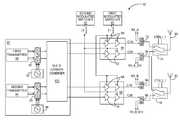
- FIG. 1is a schematic of a related art front end radio architecture (FERA) 10 that is not configured to accept power from power management architectures that employ envelope following.
- the FERA 10includes a transmitter block 12 for transmitting LTE Advanced multi-carrier signals.
- the FERA 10also includes a first power amplifier (PA) 14 powered by a first switcher 16 and a second PA 18 powered by a second switcher 20 .
- PApower amplifier
- a first duplexer 22 for an RF band A and a first receive (RX) diversity/multiple-input multiple-output (MIMO) filter 24 for an RF band Bare coupled between the first PA 14 and a first band switch 26 .
- the first duplexer 22 and the first RX diversity/MIMO filter 24are selectively coupled to a first antenna 28 through the first band switch 26 .
- the first duplexer 22outputs signals RX_A captured by the first antenna 28 .
- the first RX diversity/MIMO filter 24outputs signals RX_B_DIV also captured by the first antenna 28 .
- the band switch 26is controlled by a control signal CTRL 1 .
- a second duplexer 30 for the RF band B and a second RX diversity/MIMO filter 32are coupled between the second PA 18 and a second band switch 34 .
- the second duplexer 30is selectively coupled to a second antenna 36 through the second band switch 34 .
- the second duplexer 30outputs signals RX_B captured by the second antenna 36 .
- the second RX diversity/MIMO filter 32outputs signals RX_A_DIV also captured by the second antenna 36 .
- the transmitter block 12includes a first transmitter 38 , a first RF modulator 40 , a first radio frequency (RF) phase locked loop (PLL) 42 , a second transmitter 44 , a second RF modulator 46 , and a second RF PLL 48 .
- the transmitter block 12further includes a multi-carrier combiner 50 for combining signals output from the first RF modulator 40 and the second RF modulator 46 .
- the related art FERA 10can operate in an intra-band multi-carrier mode.
- the first transmitter 38outputs analog baseband (ABB) signals to the first RF modulator 40 .
- the second transmitter 44outputs ABB signals to the second RF modulator 46 .
- the first RF modulator 40in cooperation with the first RF PLL 42 outputs a first carrier within the RF band A while the second RF modulator 46 in cooperation with the second RF PLL 48 outputs a second carrier that is also within the band A.
- the first PA 14provides power amplification of the first carrier and the second carrier which are output through the first duplexer 22 to the first antenna 28 .
- the related art FERA 10also includes an inter-band multicarrier mode.
- the first RF modulator 40in cooperation with the first RF PLL 42 outputs a first carrier within the RF band A while the second RF modulator 46 in cooperation with the second RF PLL 48 outputs a second carrier within the RF band B.
- the first PA 14provides power amplification of the first carrier which is output through the first duplexer 22 to the first antenna 28 .
- the second PA 18provides power amplification of the second carrier which is output through the second duplexer 30 to the second antenna 36 .
- the related art FERA 10offers a realizable architecture for LTE-Advanced operation
- the related art FERA 10is wasteful with regard to energy, in that the FERA 10 is not structured to take advantage of a high energy efficiency operation provided by envelope following systems.
- Energy efficiency in battery powered user equipment (UE)such as mobile terminals that implement LTE-Advanced operation is very important, since a relatively long operation time between battery charges is desirable.
- UEbattery powered user equipment
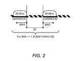
- FIG. 2is a spectrum diagram that illustrates a common collector voltage (VCC) bandwidth (BW) switcher modulation requirement for intra-band dual carrier transmission.
- VCCcommon collector voltage
- BWbandwidth
- the modulation bandwidth of the switcher 16 ( FIG. 1 ) and the switcher 20 ( FIG. 1 )is a function of an offset frequency Df between a carrier # 1 and a carrier # 2 . Therefore, the higher the offset frequency Df between the carrier # 1 and the carrier # 2 , the higher the modulation bandwidth must be. At some point, the offset frequency Df is large enough that related art approaches for modulating a VCC pseudo envelope following (PEF) signal via either the switcher 16 or the switcher 20 are no longer practical.
- PEFVCC pseudo envelope following
- the supply modulation bandwidth needed for envelope trackingis about 1.5 ⁇ (40 MHz+20 MHz) or about 90 MHz for LTE-Advanced carriers having around 20 MHz of bandwidth.
- a multiplier of 1.5is a result of a square root operation of PEF calculation.
- the offset frequency Dfis equal to zero between two adjacent carriers having a 20 MHz bandwidth each, a resulting 50 MHz VCC BW is too large for efficient modulation of the VCC PEF via either the switcher 16 or the switcher 20 .
- Embodiments of the present disclosureprovide a front end radio architecture (FERA) and power management architecture for LTE-Advanced operation.
- the FERAincludes a first power amplifier (PA) block having a first-first PA and a first-second PA, and a second PA block having a second-first PA and a second-second PA.
- First and second modulated switchersare adapted to selectively supply power to the first-first PA and the second-first PA, and to supply power to the first-second PA and the second-second PA, respectively.
- the first and second modulated switchershave a modulation bandwidth of at least 20 MHz and are both suitable for envelope tracking modulation.
- a control systemis adapted to selectively enable and disable the first-first PA, first-second PA, the second-first PA, and the second-second PA.
- First and second switchesare responsive to control signals to route carriers and received signals between first and second antennas depending upon a selectable mode of operation such as intra-band or inter-band operation.
- the first modulated switcheris adapted to supply power to the first-first PA and the second-first PA, while the second modulated switcher is adapted to supply power to the first-second PA and the second-second PA.
- the first switchhas a first control input, a first throw terminal, a second throw terminal, and a first pole terminal coupled to a first throw and a second throw, wherein the first switch is responsive to a first control signal to selectively close and open the first throw with the first throw terminal, and to selectively close and open the second throw with the second throw terminal.
- the second switchhas a second control input, a third throw terminal, a fourth throw terminal, and a second pole terminal coupled to a third throw and a fourth throw, wherein the second switch is responsive to a second control signal to selectively close and open the third throw with the third throw terminal, and to selectively close and open the fourth throw with the fourth throw terminal.
- the first duplexeris coupled between an output of the first-first PA and the first throw terminal, whereas the second duplexer is coupled between an output of the first-second PA and the second throw terminal.
- the third duplexeris coupled between an output of the second-first PA and the third throw terminal, whereas a fourth duplexer is coupled between an output of the second-second PA and the fourth throw terminal.
- the control systemis adapted to selectively enable and disable the first-first PA, the first-second PA, the second-first PA, and the second-second PA, and to provide the first control signal and the second control signal.
- FIG. 1is a schematic of a related art front end radio architecture (FERA) that is not configured to accept power from power management architectures that employ envelope following.
- FERAfront end radio architecture
- FIG. 2is a spectrum diagram that illustrates a common collector voltage (VCC) bandwidth (BW) switcher modulation requirement for intra-band dual carrier transmission.
- VCCcommon collector voltage
- BWbandwidth
- FIG. 3is a schematic of a FERA that in accordance with the present disclosure is configured for operation with envelope following techniques.
- FIG. 4is a schematic of the FERA during intra-band operation for band A.
- FIG. 5is a schematic of the FERA during intra-band operation for band B.
- FIG. 6is a schematic of the FERA during intra-band operation between band A and band B.
- FIG. 7is a schematic of the FERA during intra-band operation between band A and band B with receive diversity using MIMO.
- FIG. 8is a schematic of the FERA during intra-band operation between band A and band B with receive diversity/MIMO and swapped carrier transmission.
- FIG. 9is a schematic of the FERA that is modified to reduce BOM costs by including split band duplexers for band A.
- FIG. 10is a schematic of the FERA that is modified to reduce BOM costs by including split band duplexers for band B.
- FIG. 11depicts a mobile terminal that incorporates the FERA of the present disclosure.
- Embodiments of the present disclosureprovide front end radio architecture (FERA) and power management architecture for LTE-Advanced operation.
- FERAfront end radio architecture
- the FERA and power management of the present disclosureis configured to employ envelope following that is compatible with existing bandwidth limited to 20 MHz LTE-Advanced for dual carriers implemented in both intra-band and inter-band scenarios.
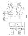
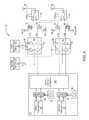
- FIG. 3is a schematic of a FERA 52 that in accordance with the present disclosure is configured for operation with envelope following techniques.
- the FERA 52includes a transmitter block 54 for transmitting LTE Advanced multi-carrier signals.
- the FERA 52also includes a first PA block 56 having a first-first PA 58 that is selectively powered by a first modulated switcher 60 and a first-second PA 62 that is selectively powered by a second modulated switcher 64 .
- the FERA 52further includes a second PA block 66 having a second-first PA 68 that is selectively powered by the first modulated switcher 60 and a second-second PA 70 that is selectively powered by the second modulated switcher 64 .
- the first modulated switcher 60has a first output filter comprising a first inductor L 1
- the second modulated switcher 64includes a second output filter comprising a second inductor L 2 .
- a first duplexer 72 for a first band A carrier C 1 A and a band A receive signal RX_Ais coupled between an output of the first-first PA 58 and a first terminal of a first single pole double throw (SP2T) switch 74 .
- a second duplexer 76 for a second band A carrier C 2 A and a band A diversity/MIMO receive signal RX_A_Divis coupled between an output of the first-second PA 62 and a first terminal of a second SP2T switch 78 .
- the first duplexer 72is selectively coupled to a first antenna 80 through the first SP2T switch 74 .
- the first duplexer 72outputs the receive signal RX_A captured by the first antenna 80 .
- the second duplexer 76is selectively coupled to a second antenna 82 through the second SP2T switch 78 .
- the second duplexer 76outputs the diversity/MIMO receive signal RX_A_DIV captured by the second antenna 82 .
- the first SP2T switch 74is controllable by a first control signal CTRL 1 _ 1
- the second SP2T switch 78is controllable by a second control signal CTRL 2 _ 1 .
- a third duplexer 84 for a first band B carrier C 1 B and a band B receive signal RX_Bis coupled between an output of the second-first PA 68 and a second terminal of the first SP2T switch 74 .
- a fourth duplexer 86 for a second band B carrier C 2 B and a band B diversity/MIMO receive signal RX_B_Divis coupled between an output of the second-second PA 70 and a second terminal of a second SP2T switch 78 .
- the third duplexer 84is selectively coupled to the first antenna 80 through the first SP2T switch 74 .
- the third duplexer 84outputs the receive signal RX_B captured by the first antenna 80 .
- the fourth duplexer 86is selectively coupled to the second antenna 82 through the second SP2T switch 78 .
- the fourth duplexer 86outputs the diversity/MIMO receive signal RX_B_DIV captured by the second antenna 82 .
- the transmitter block 54includes a first transmitter 88 , a first RF modulator 90 , a first radio frequency (RF) phase locked loop (PLL) 92 , a second transmitter 94 , a second RF modulator 96 , and a second RF PLL 98 .
- the transmitter block 54further includes a multi-carrier combiner 100 for combining signals output from the first RF modulator 90 and the second RF modulator 96 .
- the FERA 52can operate in an intra-band multi-carrier mode.
- the first transmitter 88outputs analog baseband (ABB) signals to the first RF modulator 90 .
- the second transmitter 94outputs ABB signals to the second RF modulator 96 .
- the first RF modulator 90in cooperation with the first RF PLL 92 outputs a first carrier, C 1 A, within RF band A while the second RF modulator 96 in cooperation with the second RF PLL 98 outputs a second carrier, C 2 A, that is also within the band A.
- the first-first PA 58provides power amplification of the first carrier, C 1 A, which is output through the first duplexer 72 to the first antenna 80 .
- the first-second PA 62provides power amplification of the second carrier, C 2 A, which is output through the second duplexer 76 to the second antenna 82 .
- the FERA 52also includes an inter-band multicarrier mode.
- the first RF modulator 90in cooperation with the first RF PLL 92 outputs a first carrier within the RF band A while the second RF modulator 96 in cooperation with the second RF PLL 98 outputs a second carrier within the RF band B.
- the first PA block 56provides power amplification of the first carrier, which is output through the first duplexer 72 to the first antenna 80 .
- the second PA block 66provides power amplification of the second carrier, which is output through the fourth duplexer 86 to the second antenna 82 .
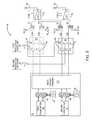
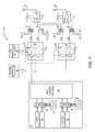
- FIG. 4is a schematic of the FERA 52 during intra-band operation for band A. Dashed lines in FIG. 4 represent deactivated or unused components.
- the second PA block 66is deactivated, while the third duplexer 84 and the fourth duplexer 86 are unused.
- the first PA block 56remains completely energized with the first-first PA 58 being supplied with power from the first modulated switcher 60 and the first-second PA 62 being supplied with power from the second modulated switcher 64 .
- the CTRL 1 _ 1 signalcloses the first throw of the first SP2T switch 74 so that the first carrier C 1 A is transmitted from the first antenna 80 , while the band A receive signal RX_A is captured by the first antenna 80 and output from the first duplexer 72 .
- the CTRL 2 _ 1 signalcloses a first throw of the second SP2T switch 78 so that the second carrier C 2 A is transmitted from the second antenna 82 , and so that the band A diversity/MIMO receive signal RX_A_DIV captured by the second antenna 82 is output from the second duplexer 76 .
- FIG. 5is a schematic of the FERA 52 during intra-band operation for band B. Dashed lines in FIG. 5 represent deactivated or unused components.
- the first PA block 56is deactivated, while the first duplexer 72 and the second duplexer 76 are unused.
- the second PA block 66remains completely energized with the second-first PA 68 being supplied with power from the first modulated switcher 60 , and the second-second PA 70 being supplied with power from the second modulated switcher 64 .
- the CTRL 1 _ 1 signalcloses a second throw of the first SP2T switch 74 so that the first carrier C 1 B is transmitted from the first antenna 80 , and so that the band B receive signal RX_B captured by the first antenna 80 is output from the third duplexer 84 .
- the CTRL 2 _ 1 signalcloses a second throw of the second SP2T switch 78 so that the second carrier C 2 B is transmitted from the second antenna 82 , and so that the band B diversity/MIMO receive signal RX_B_DIV captured by the second antenna 82 is output from the fourth duplexer 86 .
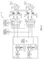
- FIG. 6is a schematic of the FERA 52 during intra-band operation between band A and band B. Dashed lines represent deactivated or unused components.
- the first PA block 56 and the second PA block 66are only partially energized.
- the first-first PA 58is powered by the first modulated switcher 60 and the second-second PA 70 is powered by the second modulated switcher 64 , while the second-first PA 68 and the first-second PA 62 are deactivated.
- the second duplexer 76 and the third duplexer 84are unused.
- the control signal CTRL 1 _ 1closes the first throw of the first SP2T switch 74 so that the first carrier C 1 A is transmitted from the first antenna 80 , and so that the band A receive signal RX_A is output from the first duplexer 72 .
- the control signal CTRL 2 _ 1closes the second throw of the second SP2T switch 78 so that the second carrier C 2 B is transmitted from the second antenna 82 , and so that the diversity/MIMO receive signal RX_B_DIV is output from the fourth duplexer 86 .
- FIG. 7is a schematic of the FERA 52 during intra-band operation between band A and band B with receive diversity using MIMO. Dashed lines represent deactivated or unused components.
- the first PA block 56 and the second PA block 66are only partially energized as in FIG. 6 .
- the first and second throws of the first SP2T switch 74 and the second switch 78are closed by the control signals CTRL 1 _ 1 and CTRL 2 _ 1 .
- the first carrier C 1 Ais transmitted from the first antenna 80 , while the band A receive signal RX_A captured by the first antenna 80 is output from the first duplexer 72 , and the diversity/MIMO receive signal RX_A_DIV captured by the second antenna 82 is output from the second duplexer 76 .
- the second carrier C 2 Bis transmitted from the second antenna 82 , while the band B receive signal RX_B captured by the first antenna 80 is output from the third duplexer 84 , and the diversity/MIMO receive signal RX_B_DIV captured by the second antenna 82 is output from the fourth duplexer 86 .
- FIG. 8is a schematic of the FERA 52 during intra-band operation between band A and band B with receive diversity using MIMO and swapped carrier transmission. Dashed lines represent deactivated or unused components.
- the first PA block 56 and the second PA block 66are only partially energized.
- the first-first PA 58 and the second-second PA 70are deactivated, while the second first PA 68 is energized by the first modulated switcher 60 and the first-second PA 62 is energized by the second modulated switcher 64 .
- the first and second throws of the first SP2T switch 74 and the second switch 78remain closed by the control signals CTRL 1 _ 1 and CTRL 2 _ 1 .
- the band A receive signal RX_A captured by the first antenna 80is output from the first duplexer 72
- the band B receive signal RX_B also captured by first antenna 80is output from the third duplexer 84
- the band A diversity/MIMO receive signal RX_A_DIV captured by the second antenna 82is output from the second duplexer 76
- the band B diversity/MIMO receive signalis output from the fourth duplexer 86 .
- the carrier C 2 Ais transmitted from the second antenna 82
- the carrier C 1 Bis transmitted from the first antenna 80 .
- the FERA 52allows envelope tracking for dual carriers in both intra-band and inter-band operation, which eliminates a need for an extra 1 dB of PAR. As a result, the FERA 52 offers improved efficiency for dual carrier operation. Moreover, intermodulation distortion is reduced due to separated transmitter chains comprised of the first PA block 56 and the second PA block 66 . Further still, the configuration of the first SP2T switch 74 and the second SP2T switch 78 combined with the first duplexer 72 , the second duplexer 76 , the third duplexer 84 , and the fourth duplexer 86 allows for carrier transmission diversity. However, these advantages offered by the FERA 52 come with an increased bill of materials (BOM) cost of an extra TX filter per band. Also, unless the extra complexity of a half-power split type amplifier is implemented an additional cost of an extra PA block is included in the FERA 52 .
- BOMbill of materials
- FIG. 9is a schematic of the FERA 52 that is modified to reduce BOM costs by replacing the first duplexer 72 with a first split band duplexer 102 , and by replacing the second duplexer 76 with a second split band duplexer 104 .
- the first split band duplexer 102includes a first TX filter 106 for passing the carrier C 1 A located in the lower half TX band of band A.
- the second split band duplexer 104includes a second TX filter 108 for passing the carrier C 2 A located in the upper half TX band of band A.
- the combined bandwidth of the first TX filter 106 and the second TX filter 108is adaptable to cover the upper and lower halves of a given TX band.
- FIG. 10is a schematic of the FERA 52 that is also modified to reduce BOM costs by replacing the third duplexer 84 with a third split band duplexer 103 , and by replacing the fourth duplexer 86 with a fourth split band duplexer 105 .
- a third TX filter 107passes the carrier C 1 B located in the lower half TX band of band B.
- a fourth TX filter 109passes the carrier C 2 B located in the upper half TX band of band B.
- One modification to the FERA 52would allow a transmission of both halves of band A from the first antenna 80 and both halves of band B from the other antenna 82 by tuning the first PA block 56 for the carriers C 1 A and C 1 B, and the second PA block 66 for the carriers C 2 A and C 2 B.
- the first modulated switcher 60would supply the second-second PA 70 and the second modulated switcher 64 would supply the second-first PA 68 .
- the first antenna 80would only be associated with band A and the second antenna 82 would only be associated with band B.
- IMDcould be an issue with this implementation since the two half band carriers may not have enough antenna isolation between them.
- the RX_A_DIV output and the RX_B_DIV outputcould remain as is shown in FIG. 3 .
- the resulting receiver and transmitter separationwould be relatively large. Thus, reducing the design requirements for filtering.
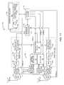
- FIG. 11depicts user equipment (UE) in the form of a mobile terminal 110 that incorporates a preferred embodiment of the FERA 52 of the present disclosure.
- the mobile terminal 110may be, but is not limited to, a mobile telephone, a personal digital assistant (PDA), or the like.
- the basic architecture of the mobile terminal 110may also include a baseband processor 112 , a control system 114 , and an interface 116 .
- the first antenna 80receives information-bearing RF signals from one or more remote transmitters provided by a base station (not shown).
- the first switch 74under the control of the CTRL 1 _ 1 signal output from the control system 114 allows the information-bearing RF signals to feed through the first duplexer 72 and into a band A RX 118 .
- the band A RX 118includes a low noise amplifier (LNA) 120 that amplifies the signal, and a first filter circuit 122 that minimizes broadband interference in the received signals.
- the band A RX 118also includes downconversion and digitization circuitry 124 , which downconverts the filtered, received signals to intermediate or baseband frequency signals, which are then digitized into one or more digital streams.
- LNAlow noise amplifier
- the second antenna 82receives information-bearing RF signals from one or more remote transmitters provided by a base station (not shown).
- the second switch 78under the control of the CTRL 2 _ 1 signal output from the control system 114 allows the information-bearing signals to feed through the fourth duplexer 86 and into a band B RX 126 .
- the band B RX 126includes a second LNA 128 that amplifies the signals, and a second filter circuit 130 that minimizes broadband interference in the received signals.
- the band B RX 126also includes downconversion and digitization circuitry 132 , which downconverts the filtered, received signals to intermediate or baseband frequency signals, which are then digitized into one or more digital streams.
- the baseband processor 112processes the digitized received signals to extract the information or data bits conveyed in the received signals. This processing typically comprises demodulation, decoding, and error correction operations. As such, the baseband processor 112 is generally implemented in one or more digital signal processors (DSPs).
- DSPsdigital signal processors
- the baseband processor 112receives digitized data, which may represent voice, data, or control information, which it encodes for transmission, from the control system 114 .
- the encoded datais output to the transmitter block 54 .
- the PA blocks 56 and 66amplify the carriers C 1 A, C 2 A, C 1 B, and C 2 B to levels appropriate for transmission from the first antenna 80 and the second antenna 82 . Different combinations of the carriers C 1 A, C 2 A, C 1 B, and C 2 B may also be transmitted from the first antenna 80 and the second antenna 82 under control of the control signals CTRL 1 _ 1 and CTRL 2 _ 1 , as described previously.
- a usermay interact with the mobile terminal 110 via the interface 116 , which may include interface circuitry 134 associated with a microphone 136 , a speaker 138 , a keypad 140 , and a display 142 .
- the interface circuitry 134typically includes analog-to-digital converters, digital-to-analog converters, amplifiers, and the like. Additionally, it may include a voice encoder/decoder, in which case it may communicate directly with the baseband processor 112 .
- the microphone 136will typically convert audio input, such as the user's voice, into an electrical signal, which is then digitized and passed directly or indirectly to the baseband processor 112 . Audio information encoded in the received signal is recovered by the baseband processor 112 and converted by the interface circuitry 134 into an analog signal suitable for driving the speaker 138 .
- the keypad 140 and the display 142enable the user to interact with the mobile terminal 110 , inputting numbers to be dialed, address book information, or the like, as well as monitoring call progress information.
Landscapes
- Engineering & Computer Science (AREA)
- Power Engineering (AREA)
- Signal Processing (AREA)
- Computer Networks & Wireless Communication (AREA)
- Transmitters (AREA)
Abstract
Description
Claims (26)
Priority Applications (2)
| Application Number | Priority Date | Filing Date | Title |
|---|---|---|---|
| US13/460,861US8774065B2 (en) | 2011-05-02 | 2012-05-01 | Radio front end and power management architecture for LTE-advanced |
| US14/051,601US9220067B2 (en) | 2011-05-02 | 2013-10-11 | Front end radio architecture (FERA) with power management |
Applications Claiming Priority (2)
| Application Number | Priority Date | Filing Date | Title |
|---|---|---|---|
| US201161481311P | 2011-05-02 | 2011-05-02 | |
| US13/460,861US8774065B2 (en) | 2011-05-02 | 2012-05-01 | Radio front end and power management architecture for LTE-advanced |
Related Child Applications (1)
| Application Number | Title | Priority Date | Filing Date |
|---|---|---|---|
| US14/051,601Continuation-In-PartUS9220067B2 (en) | 2011-05-02 | 2013-10-11 | Front end radio architecture (FERA) with power management |
Publications (2)
| Publication Number | Publication Date |
|---|---|
| US20120281597A1 US20120281597A1 (en) | 2012-11-08 |
| US8774065B2true US8774065B2 (en) | 2014-07-08 |
Family
ID=47090182
Family Applications (1)
| Application Number | Title | Priority Date | Filing Date |
|---|---|---|---|
| US13/460,861Active2032-09-16US8774065B2 (en) | 2011-05-02 | 2012-05-01 | Radio front end and power management architecture for LTE-advanced |
Country Status (1)
| Country | Link |
|---|---|
| US (1) | US8774065B2 (en) |
Cited By (52)
| Publication number | Priority date | Publication date | Assignee | Title |
|---|---|---|---|---|
| US9078211B2 (en) | 2012-10-11 | 2015-07-07 | Rf Micro Devices, Inc. | Power management configuration for TX MIMO and UL carrier aggregation |
| US9143208B2 (en) | 2012-07-18 | 2015-09-22 | Rf Micro Devices, Inc. | Radio front end having reduced diversity switch linearity requirement |
| US9172441B2 (en) | 2013-02-08 | 2015-10-27 | Rf Micro Devices, Inc. | Front end circuitry for carrier aggregation configurations |
| US9203596B2 (en) | 2012-10-02 | 2015-12-01 | Rf Micro Devices, Inc. | Tunable diplexer for carrier aggregation applications |
| US9219594B2 (en) | 2012-06-18 | 2015-12-22 | Rf Micro Devices, Inc. | Dual antenna integrated carrier aggregation front end solution |
| US9220067B2 (en) | 2011-05-02 | 2015-12-22 | Rf Micro Devices, Inc. | Front end radio architecture (FERA) with power management |
| US9515622B2 (en) | 2014-12-23 | 2016-12-06 | Nokia Technologies Oy | Reconfigurable bias and supply drivers for radio frequency power amplifiers |
| US9991065B2 (en) | 2012-07-11 | 2018-06-05 | Qorvo Us, Inc. | Contact MEMS architecture for improved cycle count and hot-switching and ESD |
| US10326490B2 (en) | 2017-08-31 | 2019-06-18 | Qorvo Us, Inc. | Multi radio access technology power management circuit |
| US10439557B2 (en) | 2018-01-15 | 2019-10-08 | Qorvo Us, Inc. | Envelope tracking power management circuit |
| US10530311B2 (en) | 2017-04-25 | 2020-01-07 | Qorvo Us, Inc. | Envelope tracking amplifier circuit |
| US10530305B2 (en) | 2017-10-06 | 2020-01-07 | Qorvo Us, Inc. | Nonlinear bandwidth compression circuitry |
| US10637408B2 (en) | 2018-01-18 | 2020-04-28 | Qorvo Us, Inc. | Envelope tracking voltage tracker circuit and related power management circuit |
| US10680556B2 (en) | 2018-11-05 | 2020-06-09 | Qorvo Us, Inc. | Radio frequency front-end circuit |
| US10742170B2 (en) | 2018-02-01 | 2020-08-11 | Qorvo Us, Inc. | Envelope tracking circuit and related power amplifier system |
| US10797649B2 (en) | 2017-07-17 | 2020-10-06 | Qorvo Us, Inc. | Multi-mode envelope tracking amplifier circuit |
| US10911001B2 (en) | 2018-10-02 | 2021-02-02 | Qorvo Us, Inc. | Envelope tracking amplifier circuit |
| US10938351B2 (en) | 2018-10-31 | 2021-03-02 | Qorvo Us, Inc. | Envelope tracking system |
| US10944365B2 (en) | 2018-06-28 | 2021-03-09 | Qorvo Us, Inc. | Envelope tracking amplifier circuit |
| US10985702B2 (en) | 2018-10-31 | 2021-04-20 | Qorvo Us, Inc. | Envelope tracking system |
| US10998859B2 (en) | 2019-02-07 | 2021-05-04 | Qorvo Us, Inc. | Dual-input envelope tracking integrated circuit and related apparatus |
| US11018638B2 (en) | 2018-10-31 | 2021-05-25 | Qorvo Us, Inc. | Multimode envelope tracking circuit and related apparatus |
| US11018627B2 (en) | 2019-04-17 | 2021-05-25 | Qorvo Us, Inc. | Multi-bandwidth envelope tracking integrated circuit and related apparatus |
| US11025458B2 (en) | 2019-02-07 | 2021-06-01 | Qorvo Us, Inc. | Adaptive frequency equalizer for wide modulation bandwidth envelope tracking |
| US11031911B2 (en) | 2019-05-02 | 2021-06-08 | Qorvo Us, Inc. | Envelope tracking integrated circuit and related apparatus |
| US11031909B2 (en) | 2018-12-04 | 2021-06-08 | Qorvo Us, Inc. | Group delay optimization circuit and related apparatus |
| US11082007B2 (en) | 2018-12-19 | 2021-08-03 | Qorvo Us, Inc. | Envelope tracking integrated circuit and related apparatus |
| US11082009B2 (en) | 2019-04-12 | 2021-08-03 | Qorvo Us, Inc. | Envelope tracking power amplifier apparatus |
| US11088618B2 (en) | 2018-09-05 | 2021-08-10 | Qorvo Us, Inc. | PWM DC-DC converter with linear voltage regulator for DC assist |
| US11146213B2 (en) | 2019-01-15 | 2021-10-12 | Qorvo Us, Inc. | Multi-radio access technology envelope tracking amplifier apparatus |
| US11196392B2 (en) | 2020-03-30 | 2021-12-07 | Qorvo Us, Inc. | Device and device protection system |
| US11233481B2 (en) | 2019-02-18 | 2022-01-25 | Qorvo Us, Inc. | Modulated power apparatus |
| US11309922B2 (en) | 2019-12-13 | 2022-04-19 | Qorvo Us, Inc. | Multi-mode power management integrated circuit in a small formfactor wireless apparatus |
| US11349513B2 (en) | 2019-12-20 | 2022-05-31 | Qorvo Us, Inc. | Envelope tracking system |
| US11349436B2 (en) | 2019-05-30 | 2022-05-31 | Qorvo Us, Inc. | Envelope tracking integrated circuit |
| US11374482B2 (en) | 2019-04-02 | 2022-06-28 | Qorvo Us, Inc. | Dual-modulation power management circuit |
| US11424719B2 (en) | 2019-04-18 | 2022-08-23 | Qorvo Us, Inc. | Multi-bandwidth envelope tracking integrated circuit |
| US11539289B2 (en) | 2019-08-02 | 2022-12-27 | Qorvo Us, Inc. | Multi-level charge pump circuit |
| US11539330B2 (en) | 2020-01-17 | 2022-12-27 | Qorvo Us, Inc. | Envelope tracking integrated circuit supporting multiple types of power amplifiers |
| US11588449B2 (en) | 2020-09-25 | 2023-02-21 | Qorvo Us, Inc. | Envelope tracking power amplifier apparatus |
| US11716057B2 (en) | 2020-01-28 | 2023-08-01 | Qorvo Us, Inc. | Envelope tracking circuitry |
| US11728774B2 (en) | 2020-02-26 | 2023-08-15 | Qorvo Us, Inc. | Average power tracking power management integrated circuit |
| US11728796B2 (en) | 2020-10-14 | 2023-08-15 | Qorvo Us, Inc. | Inverted group delay circuit |
| US20240048105A1 (en)* | 2020-06-30 | 2024-02-08 | Apple Inc. | Multi-frequency band communication based on filter sharing |
| US11909385B2 (en) | 2020-10-19 | 2024-02-20 | Qorvo Us, Inc. | Fast-switching power management circuit and related apparatus |
| US12063018B2 (en) | 2021-06-10 | 2024-08-13 | Qorvo Us, Inc. | Envelope tracking integrated circuit operable with multiple types of power amplifiers |
| US12068720B2 (en) | 2021-02-26 | 2024-08-20 | Qorvo Us, Inc. | Barely Doherty dual envelope tracking (BD2E) circuit |
| US12126305B2 (en) | 2021-05-27 | 2024-10-22 | Qorvo Us, Inc. | Radio frequency (RF) equalizer in an envelope tracking (ET) circuit |
| US12212285B2 (en) | 2020-12-22 | 2025-01-28 | Qorvo Us, Inc. | Power management apparatus operable with multiple configurations |
| US12212286B2 (en) | 2021-03-05 | 2025-01-28 | Qorvo Us, Inc. | Complementary envelope detector |
| US12267046B2 (en) | 2021-02-15 | 2025-04-01 | Qorvo Us, Inc. | Power amplifier system |
| US12265442B2 (en) | 2020-12-04 | 2025-04-01 | Qorvo Us, Inc. | Power management integrated circuit |
Families Citing this family (16)
| Publication number | Priority date | Publication date | Assignee | Title |
|---|---|---|---|---|
| EP2856654A4 (en)* | 2012-06-05 | 2016-03-09 | Rivada Networks Llc | Method and system for providing diverse multiple carrier aggregation |
| TWI445332B (en)* | 2012-06-18 | 2014-07-11 | Hon Hai Prec Ind Co Ltd | Multiple input multiple output transceiver |
| US9185705B2 (en)* | 2012-06-19 | 2015-11-10 | Samsung Electronics Co., Ltd. | Apparatus and methods for flexible RF configuration in multi-antenna wireless systems |
| US20140328436A1 (en)* | 2013-05-03 | 2014-11-06 | Nvidia Corporation | Receiver front-end architecture for carrier aggregation |
| GB2519361B (en)* | 2013-10-21 | 2015-09-16 | Nujira Ltd | Reduced bandwidth of signal in an envelope path for envelope tracking system |
| US20150109977A1 (en)* | 2013-10-21 | 2015-04-23 | Samsung Electronics Co., Ltd. | Front end configurations supporting inter-band carrier aggregation |
| WO2015168403A1 (en)* | 2014-05-01 | 2015-11-05 | Paragon Communications, Ltd. | Method and apparatus for multiple-output partial envelope tracking |
| US9941908B2 (en) | 2014-10-20 | 2018-04-10 | Infineon Technologies Ag | System and method for a radio frequency filter |
| US9860898B1 (en) | 2015-11-16 | 2018-01-02 | Sprint Communications Company L.P. | Long term evolution (LTE) network control of carrier aggregation for user equipment |
| US10749274B2 (en) | 2016-02-19 | 2020-08-18 | Hewlett-Packard Development Company, L.P. | Separate antenna |
| US10171037B2 (en) | 2017-04-25 | 2019-01-01 | Qorvo Us, Inc. | Multi-mode power management system supporting fifth-generation new radio |
| US10879852B2 (en) | 2017-08-08 | 2020-12-29 | Qorvo Us, Inc. | Power management circuit and related radio frequency front-end circuit |
| US10090809B1 (en)* | 2017-08-15 | 2018-10-02 | Qorvo Us, Inc. | Multi-mode mobile power management circuit |
| US10326408B2 (en) | 2017-09-18 | 2019-06-18 | Qorvo Us, Inc. | Envelope tracking power management circuit |
| US10553530B2 (en) | 2017-09-29 | 2020-02-04 | Qorvo Us, Inc. | Three-dimensional (3D) inductor-capacitor (LC) circuit |
| US10361667B2 (en) | 2017-12-08 | 2019-07-23 | Qorvo Us, Inc. | Low noise amplifier circuit |
Citations (7)
| Publication number | Priority date | Publication date | Assignee | Title |
|---|---|---|---|---|
| US20060012425A1 (en)* | 2001-07-31 | 2006-01-19 | Renesas Technology Corp. | Radio frequency power amplifier |
| US20080003797A1 (en) | 2006-06-29 | 2008-01-03 | Hynix Semiconductor Inc. | Method for forming tungsten layer of semiconductor device and method for forming tungsten wiring layer using the same |
| US20090180403A1 (en) | 2008-01-11 | 2009-07-16 | Bogdan Tudosoiu | Multi-band and multi-mode radio frequency front-end module architecture |
| US20100099366A1 (en) | 2002-04-22 | 2010-04-22 | Ipr Licensing, Inc. | Multiple-input multiple-output radio transceiver |
| US20110241787A1 (en) | 2010-03-30 | 2011-10-06 | Stefan Mastovich | Technique for detecting crystals |
| US20120235735A1 (en) | 2009-12-03 | 2012-09-20 | Erwin Spits | Power amplifier circuit and front end circuit |
| US20120320803A1 (en) | 2010-12-15 | 2012-12-20 | Skarp Filip | Wireless Terminals Including Smart Antenna Systems Having Multiple Antennas |
- 2012
- 2012-05-01USUS13/460,861patent/US8774065B2/enactiveActive
Patent Citations (7)
| Publication number | Priority date | Publication date | Assignee | Title |
|---|---|---|---|---|
| US20060012425A1 (en)* | 2001-07-31 | 2006-01-19 | Renesas Technology Corp. | Radio frequency power amplifier |
| US20100099366A1 (en) | 2002-04-22 | 2010-04-22 | Ipr Licensing, Inc. | Multiple-input multiple-output radio transceiver |
| US20080003797A1 (en) | 2006-06-29 | 2008-01-03 | Hynix Semiconductor Inc. | Method for forming tungsten layer of semiconductor device and method for forming tungsten wiring layer using the same |
| US20090180403A1 (en) | 2008-01-11 | 2009-07-16 | Bogdan Tudosoiu | Multi-band and multi-mode radio frequency front-end module architecture |
| US20120235735A1 (en) | 2009-12-03 | 2012-09-20 | Erwin Spits | Power amplifier circuit and front end circuit |
| US20110241787A1 (en) | 2010-03-30 | 2011-10-06 | Stefan Mastovich | Technique for detecting crystals |
| US20120320803A1 (en) | 2010-12-15 | 2012-12-20 | Skarp Filip | Wireless Terminals Including Smart Antenna Systems Having Multiple Antennas |
Non-Patent Citations (3)
| Title |
|---|
| Non-Final Office Action for U.S. Appl. No. 13/045,621, mailed May 31, 2013, 13 pages. |
| Notice of Allowance for U.S. Appl. No. 13/045,604, mailed May 17, 2013, 11 pages. |
| Notice of Allowance for U.S. Appl. No. 13/045,621, mailed Sep. 24, 2013, 10 pages. |
Cited By (54)
| Publication number | Priority date | Publication date | Assignee | Title |
|---|---|---|---|---|
| US9220067B2 (en) | 2011-05-02 | 2015-12-22 | Rf Micro Devices, Inc. | Front end radio architecture (FERA) with power management |
| US9219594B2 (en) | 2012-06-18 | 2015-12-22 | Rf Micro Devices, Inc. | Dual antenna integrated carrier aggregation front end solution |
| US9991065B2 (en) | 2012-07-11 | 2018-06-05 | Qorvo Us, Inc. | Contact MEMS architecture for improved cycle count and hot-switching and ESD |
| US9143208B2 (en) | 2012-07-18 | 2015-09-22 | Rf Micro Devices, Inc. | Radio front end having reduced diversity switch linearity requirement |
| US9203596B2 (en) | 2012-10-02 | 2015-12-01 | Rf Micro Devices, Inc. | Tunable diplexer for carrier aggregation applications |
| US9078211B2 (en) | 2012-10-11 | 2015-07-07 | Rf Micro Devices, Inc. | Power management configuration for TX MIMO and UL carrier aggregation |
| US9172441B2 (en) | 2013-02-08 | 2015-10-27 | Rf Micro Devices, Inc. | Front end circuitry for carrier aggregation configurations |
| US9515622B2 (en) | 2014-12-23 | 2016-12-06 | Nokia Technologies Oy | Reconfigurable bias and supply drivers for radio frequency power amplifiers |
| US10530311B2 (en) | 2017-04-25 | 2020-01-07 | Qorvo Us, Inc. | Envelope tracking amplifier circuit |
| US10797649B2 (en) | 2017-07-17 | 2020-10-06 | Qorvo Us, Inc. | Multi-mode envelope tracking amplifier circuit |
| US11283407B2 (en) | 2017-07-17 | 2022-03-22 | Qorvo Us, Inc. | Multi-mode envelope tracking amplifier circuit |
| US10326490B2 (en) | 2017-08-31 | 2019-06-18 | Qorvo Us, Inc. | Multi radio access technology power management circuit |
| US10530305B2 (en) | 2017-10-06 | 2020-01-07 | Qorvo Us, Inc. | Nonlinear bandwidth compression circuitry |
| US10680559B2 (en) | 2017-10-06 | 2020-06-09 | Qorvo Us, Inc. | Envelope tracking system for transmitting a wide modulation bandwidth signal(s) |
| US10439557B2 (en) | 2018-01-15 | 2019-10-08 | Qorvo Us, Inc. | Envelope tracking power management circuit |
| US10637408B2 (en) | 2018-01-18 | 2020-04-28 | Qorvo Us, Inc. | Envelope tracking voltage tracker circuit and related power management circuit |
| US10742170B2 (en) | 2018-02-01 | 2020-08-11 | Qorvo Us, Inc. | Envelope tracking circuit and related power amplifier system |
| US10944365B2 (en) | 2018-06-28 | 2021-03-09 | Qorvo Us, Inc. | Envelope tracking amplifier circuit |
| US11088618B2 (en) | 2018-09-05 | 2021-08-10 | Qorvo Us, Inc. | PWM DC-DC converter with linear voltage regulator for DC assist |
| US10911001B2 (en) | 2018-10-02 | 2021-02-02 | Qorvo Us, Inc. | Envelope tracking amplifier circuit |
| US10938351B2 (en) | 2018-10-31 | 2021-03-02 | Qorvo Us, Inc. | Envelope tracking system |
| US10985702B2 (en) | 2018-10-31 | 2021-04-20 | Qorvo Us, Inc. | Envelope tracking system |
| US11018638B2 (en) | 2018-10-31 | 2021-05-25 | Qorvo Us, Inc. | Multimode envelope tracking circuit and related apparatus |
| US10680556B2 (en) | 2018-11-05 | 2020-06-09 | Qorvo Us, Inc. | Radio frequency front-end circuit |
| US11031909B2 (en) | 2018-12-04 | 2021-06-08 | Qorvo Us, Inc. | Group delay optimization circuit and related apparatus |
| US11082007B2 (en) | 2018-12-19 | 2021-08-03 | Qorvo Us, Inc. | Envelope tracking integrated circuit and related apparatus |
| US11146213B2 (en) | 2019-01-15 | 2021-10-12 | Qorvo Us, Inc. | Multi-radio access technology envelope tracking amplifier apparatus |
| US11025458B2 (en) | 2019-02-07 | 2021-06-01 | Qorvo Us, Inc. | Adaptive frequency equalizer for wide modulation bandwidth envelope tracking |
| US10998859B2 (en) | 2019-02-07 | 2021-05-04 | Qorvo Us, Inc. | Dual-input envelope tracking integrated circuit and related apparatus |
| US11233481B2 (en) | 2019-02-18 | 2022-01-25 | Qorvo Us, Inc. | Modulated power apparatus |
| US11374482B2 (en) | 2019-04-02 | 2022-06-28 | Qorvo Us, Inc. | Dual-modulation power management circuit |
| US11082009B2 (en) | 2019-04-12 | 2021-08-03 | Qorvo Us, Inc. | Envelope tracking power amplifier apparatus |
| US11018627B2 (en) | 2019-04-17 | 2021-05-25 | Qorvo Us, Inc. | Multi-bandwidth envelope tracking integrated circuit and related apparatus |
| US11424719B2 (en) | 2019-04-18 | 2022-08-23 | Qorvo Us, Inc. | Multi-bandwidth envelope tracking integrated circuit |
| US11031911B2 (en) | 2019-05-02 | 2021-06-08 | Qorvo Us, Inc. | Envelope tracking integrated circuit and related apparatus |
| US11349436B2 (en) | 2019-05-30 | 2022-05-31 | Qorvo Us, Inc. | Envelope tracking integrated circuit |
| US11539289B2 (en) | 2019-08-02 | 2022-12-27 | Qorvo Us, Inc. | Multi-level charge pump circuit |
| US11309922B2 (en) | 2019-12-13 | 2022-04-19 | Qorvo Us, Inc. | Multi-mode power management integrated circuit in a small formfactor wireless apparatus |
| US11349513B2 (en) | 2019-12-20 | 2022-05-31 | Qorvo Us, Inc. | Envelope tracking system |
| US11539330B2 (en) | 2020-01-17 | 2022-12-27 | Qorvo Us, Inc. | Envelope tracking integrated circuit supporting multiple types of power amplifiers |
| US11716057B2 (en) | 2020-01-28 | 2023-08-01 | Qorvo Us, Inc. | Envelope tracking circuitry |
| US11728774B2 (en) | 2020-02-26 | 2023-08-15 | Qorvo Us, Inc. | Average power tracking power management integrated circuit |
| US11196392B2 (en) | 2020-03-30 | 2021-12-07 | Qorvo Us, Inc. | Device and device protection system |
| US20240048105A1 (en)* | 2020-06-30 | 2024-02-08 | Apple Inc. | Multi-frequency band communication based on filter sharing |
| US11588449B2 (en) | 2020-09-25 | 2023-02-21 | Qorvo Us, Inc. | Envelope tracking power amplifier apparatus |
| US11728796B2 (en) | 2020-10-14 | 2023-08-15 | Qorvo Us, Inc. | Inverted group delay circuit |
| US11909385B2 (en) | 2020-10-19 | 2024-02-20 | Qorvo Us, Inc. | Fast-switching power management circuit and related apparatus |
| US12265442B2 (en) | 2020-12-04 | 2025-04-01 | Qorvo Us, Inc. | Power management integrated circuit |
| US12212285B2 (en) | 2020-12-22 | 2025-01-28 | Qorvo Us, Inc. | Power management apparatus operable with multiple configurations |
| US12267046B2 (en) | 2021-02-15 | 2025-04-01 | Qorvo Us, Inc. | Power amplifier system |
| US12068720B2 (en) | 2021-02-26 | 2024-08-20 | Qorvo Us, Inc. | Barely Doherty dual envelope tracking (BD2E) circuit |
| US12212286B2 (en) | 2021-03-05 | 2025-01-28 | Qorvo Us, Inc. | Complementary envelope detector |
| US12126305B2 (en) | 2021-05-27 | 2024-10-22 | Qorvo Us, Inc. | Radio frequency (RF) equalizer in an envelope tracking (ET) circuit |
| US12063018B2 (en) | 2021-06-10 | 2024-08-13 | Qorvo Us, Inc. | Envelope tracking integrated circuit operable with multiple types of power amplifiers |
Also Published As
| Publication number | Publication date |
|---|---|
| US20120281597A1 (en) | 2012-11-08 |
Similar Documents
| Publication | Publication Date | Title |
|---|---|---|
| US8774065B2 (en) | Radio front end and power management architecture for LTE-advanced | |
| US9220067B2 (en) | Front end radio architecture (FERA) with power management | |
| US8537723B2 (en) | LTE-Advanced (4G) front end radio architecture | |
| US10153789B2 (en) | Remote radio head unit system with wideband power amplifier | |
| US8552816B2 (en) | Multiband simultaneous transmission and reception front end architecture | |
| US9106453B2 (en) | Remote radio head unit system with wideband power amplifier and method | |
| US8588713B2 (en) | Power management system for multi-carriers transmitter | |
| CN103780280B (en) | Radio frequency path | |
| US8509718B2 (en) | Broadband receive only tuner combined with receive switch | |
| US9374122B2 (en) | Integrated on-chip duplexer for simultaneous wireless transmission | |
| CN101167256A (en) | Wireless transmission apparatus, polar modulation transmission apparatus, and wireless communication apparatus | |
| CN104092526B (en) | Multi-carrier communicating method and device for TDD mode MIMO wireless communicating system | |
| CN109644012A (en) | Reconfigurable radio frequency (RF) bandstop/intermediate frequency (IF) bandpass filters | |
| US20220255508A1 (en) | Load modulated doherty power amplifiers | |
| CN105141335A (en) | Antenna oscillator multiplexing method and device and antenna assembly | |
| US9071210B2 (en) | Efficient power transfer power amplifier (PA) architecture | |
| KR20130103732A (en) | Apparatus and method for a multiband radio operating in a wireless network | |
| US20230097428A1 (en) | Single matching inductor for receivers to operate frequency bands in a multi-band radio frequency device | |
| WO2018143043A1 (en) | Wireless device and wireless communication method | |
| US11923879B2 (en) | Radio unit for unsynchronized TDD multi-band operation | |
| EP2101541A1 (en) | Radio head for roads or rurual environments | |
| US20250023703A1 (en) | Multiple antenna feed for time division duplexing filter bypassing in receive carrier aggregation | |
| CN120301443A (en) | Radio frequency communication related devices | |
| CN120812705A (en) | Radio frequency front-end module, radio frequency architecture and electronic equipment |
Legal Events
| Date | Code | Title | Description |
|---|---|---|---|
| AS | Assignment | Owner name:RF MICRO DEVICES, INC., NORTH CAROLINA Free format text:ASSIGNMENT OF ASSIGNORS INTEREST;ASSIGNORS:KHLAT, NADIM;HIETALA, ALEXANDER WAYNE;SIGNING DATES FROM 20120427 TO 20120430;REEL/FRAME:028132/0562 | |
| AS | Assignment | Owner name:BANK OF AMERICA, N.A., AS ADMINISTRATIVE AGENT, TE Free format text:NOTICE OF GRANT OF SECURITY INTEREST IN PATENTS;ASSIGNOR:RF MICRO DEVICES, INC.;REEL/FRAME:030045/0831 Effective date:20130319 | |
| STCF | Information on status: patent grant | Free format text:PATENTED CASE | |
| AS | Assignment | Owner name:RF MICRO DEVICES, INC., NORTH CAROLINA Free format text:TERMINATION AND RELEASE OF SECURITY INTEREST IN PATENTS (RECORDED 3/19/13 AT REEL/FRAME 030045/0831);ASSIGNOR:BANK OF AMERICA, N.A., AS ADMINISTRATIVE AGENT;REEL/FRAME:035334/0363 Effective date:20150326 | |
| AS | Assignment | Owner name:QORVO US, INC., NORTH CAROLINA Free format text:MERGER;ASSIGNOR:RF MICRO DEVICES, INC.;REEL/FRAME:039196/0941 Effective date:20160330 | |
| FEPP | Fee payment procedure | Free format text:MAINTENANCE FEE REMINDER MAILED (ORIGINAL EVENT CODE: REM.) | |
| FEPP | Fee payment procedure | Free format text:SURCHARGE FOR LATE PAYMENT, LARGE ENTITY (ORIGINAL EVENT CODE: M1554) | |
| MAFP | Maintenance fee payment | Free format text:PAYMENT OF MAINTENANCE FEE, 4TH YEAR, LARGE ENTITY (ORIGINAL EVENT CODE: M1551) Year of fee payment:4 | |
| MAFP | Maintenance fee payment | Free format text:PAYMENT OF MAINTENANCE FEE, 8TH YEAR, LARGE ENTITY (ORIGINAL EVENT CODE: M1552); ENTITY STATUS OF PATENT OWNER: LARGE ENTITY Year of fee payment:8 |