US8772908B2 - Conductive pads defined by embedded traces - Google Patents
Conductive pads defined by embedded tracesDownload PDFInfo
- Publication number
- US8772908B2 US8772908B2US13/589,359US201213589359AUS8772908B2US 8772908 B2US8772908 B2US 8772908B2US 201213589359 AUS201213589359 AUS 201213589359AUS 8772908 B2US8772908 B2US 8772908B2
- Authority
- US
- United States
- Prior art keywords
- component
- assembly
- conductive
- conductive element
- pad
- Prior art date
- Legal status (The legal status is an assumption and is not a legal conclusion. Google has not performed a legal analysis and makes no representation as to the accuracy of the status listed.)
- Active
Links
Images


Classifications
- H—ELECTRICITY
- H01—ELECTRIC ELEMENTS
- H01L—SEMICONDUCTOR DEVICES NOT COVERED BY CLASS H10
- H01L24/00—Arrangements for connecting or disconnecting semiconductor or solid-state bodies; Methods or apparatus related thereto
- H01L24/01—Means for bonding being attached to, or being formed on, the surface to be connected, e.g. chip-to-package, die-attach, "first-level" interconnects; Manufacturing methods related thereto
- H01L24/02—Bonding areas ; Manufacturing methods related thereto
- H01L24/04—Structure, shape, material or disposition of the bonding areas prior to the connecting process
- H01L24/05—Structure, shape, material or disposition of the bonding areas prior to the connecting process of an individual bonding area
- H—ELECTRICITY
- H01—ELECTRIC ELEMENTS
- H01L—SEMICONDUCTOR DEVICES NOT COVERED BY CLASS H10
- H01L23/00—Details of semiconductor or other solid state devices
- H01L23/48—Arrangements for conducting electric current to or from the solid state body in operation, e.g. leads, terminal arrangements ; Selection of materials therefor
- H01L23/488—Arrangements for conducting electric current to or from the solid state body in operation, e.g. leads, terminal arrangements ; Selection of materials therefor consisting of soldered or bonded constructions
- H01L23/498—Leads, i.e. metallisations or lead-frames on insulating substrates, e.g. chip carriers
- H01L23/49838—Geometry or layout
- H—ELECTRICITY
- H01—ELECTRIC ELEMENTS
- H01L—SEMICONDUCTOR DEVICES NOT COVERED BY CLASS H10
- H01L24/00—Arrangements for connecting or disconnecting semiconductor or solid-state bodies; Methods or apparatus related thereto
- H01L24/01—Means for bonding being attached to, or being formed on, the surface to be connected, e.g. chip-to-package, die-attach, "first-level" interconnects; Manufacturing methods related thereto
- H01L24/02—Bonding areas ; Manufacturing methods related thereto
- H01L24/03—Manufacturing methods
- H—ELECTRICITY
- H01—ELECTRIC ELEMENTS
- H01L—SEMICONDUCTOR DEVICES NOT COVERED BY CLASS H10
- H01L2224/00—Indexing scheme for arrangements for connecting or disconnecting semiconductor or solid-state bodies and methods related thereto as covered by H01L24/00
- H01L2224/01—Means for bonding being attached to, or being formed on, the surface to be connected, e.g. chip-to-package, die-attach, "first-level" interconnects; Manufacturing methods related thereto
- H01L2224/02—Bonding areas; Manufacturing methods related thereto
- H01L2224/023—Redistribution layers [RDL] for bonding areas
- H—ELECTRICITY
- H01—ELECTRIC ELEMENTS
- H01L—SEMICONDUCTOR DEVICES NOT COVERED BY CLASS H10
- H01L2224/00—Indexing scheme for arrangements for connecting or disconnecting semiconductor or solid-state bodies and methods related thereto as covered by H01L24/00
- H01L2224/01—Means for bonding being attached to, or being formed on, the surface to be connected, e.g. chip-to-package, die-attach, "first-level" interconnects; Manufacturing methods related thereto
- H01L2224/02—Bonding areas; Manufacturing methods related thereto
- H01L2224/03—Manufacturing methods
- H01L2224/03001—Involving a temporary auxiliary member not forming part of the manufacturing apparatus, e.g. removable or sacrificial coating, film or substrate
- H01L2224/03003—Involving a temporary auxiliary member not forming part of the manufacturing apparatus, e.g. removable or sacrificial coating, film or substrate for holding or transferring a preform
- H—ELECTRICITY
- H01—ELECTRIC ELEMENTS
- H01L—SEMICONDUCTOR DEVICES NOT COVERED BY CLASS H10
- H01L2224/00—Indexing scheme for arrangements for connecting or disconnecting semiconductor or solid-state bodies and methods related thereto as covered by H01L24/00
- H01L2224/01—Means for bonding being attached to, or being formed on, the surface to be connected, e.g. chip-to-package, die-attach, "first-level" interconnects; Manufacturing methods related thereto
- H01L2224/02—Bonding areas; Manufacturing methods related thereto
- H01L2224/03—Manufacturing methods
- H01L2224/031—Manufacture and pre-treatment of the bonding area preform
- H01L2224/0311—Shaping
- H—ELECTRICITY
- H01—ELECTRIC ELEMENTS
- H01L—SEMICONDUCTOR DEVICES NOT COVERED BY CLASS H10
- H01L2224/00—Indexing scheme for arrangements for connecting or disconnecting semiconductor or solid-state bodies and methods related thereto as covered by H01L24/00
- H01L2224/01—Means for bonding being attached to, or being formed on, the surface to be connected, e.g. chip-to-package, die-attach, "first-level" interconnects; Manufacturing methods related thereto
- H01L2224/02—Bonding areas; Manufacturing methods related thereto
- H01L2224/04—Structure, shape, material or disposition of the bonding areas prior to the connecting process
- H01L2224/0401—Bonding areas specifically adapted for bump connectors, e.g. under bump metallisation [UBM]
- H—ELECTRICITY
- H01—ELECTRIC ELEMENTS
- H01L—SEMICONDUCTOR DEVICES NOT COVERED BY CLASS H10
- H01L2224/00—Indexing scheme for arrangements for connecting or disconnecting semiconductor or solid-state bodies and methods related thereto as covered by H01L24/00
- H01L2224/01—Means for bonding being attached to, or being formed on, the surface to be connected, e.g. chip-to-package, die-attach, "first-level" interconnects; Manufacturing methods related thereto
- H01L2224/02—Bonding areas; Manufacturing methods related thereto
- H01L2224/04—Structure, shape, material or disposition of the bonding areas prior to the connecting process
- H01L2224/04026—Bonding areas specifically adapted for layer connectors
- H—ELECTRICITY
- H01—ELECTRIC ELEMENTS
- H01L—SEMICONDUCTOR DEVICES NOT COVERED BY CLASS H10
- H01L2224/00—Indexing scheme for arrangements for connecting or disconnecting semiconductor or solid-state bodies and methods related thereto as covered by H01L24/00
- H01L2224/01—Means for bonding being attached to, or being formed on, the surface to be connected, e.g. chip-to-package, die-attach, "first-level" interconnects; Manufacturing methods related thereto
- H01L2224/02—Bonding areas; Manufacturing methods related thereto
- H01L2224/04—Structure, shape, material or disposition of the bonding areas prior to the connecting process
- H01L2224/05—Structure, shape, material or disposition of the bonding areas prior to the connecting process of an individual bonding area
- H01L2224/0554—External layer
- H01L2224/0555—Shape
- H01L2224/05551—Shape comprising apertures or cavities
- H—ELECTRICITY
- H01—ELECTRIC ELEMENTS
- H01L—SEMICONDUCTOR DEVICES NOT COVERED BY CLASS H10
- H01L2224/00—Indexing scheme for arrangements for connecting or disconnecting semiconductor or solid-state bodies and methods related thereto as covered by H01L24/00
- H01L2224/01—Means for bonding being attached to, or being formed on, the surface to be connected, e.g. chip-to-package, die-attach, "first-level" interconnects; Manufacturing methods related thereto
- H01L2224/02—Bonding areas; Manufacturing methods related thereto
- H01L2224/04—Structure, shape, material or disposition of the bonding areas prior to the connecting process
- H01L2224/05—Structure, shape, material or disposition of the bonding areas prior to the connecting process of an individual bonding area
- H01L2224/0554—External layer
- H01L2224/0555—Shape
- H01L2224/05552—Shape in top view
- H01L2224/05555—Shape in top view being circular or elliptic
- H—ELECTRICITY
- H01—ELECTRIC ELEMENTS
- H01L—SEMICONDUCTOR DEVICES NOT COVERED BY CLASS H10
- H01L2224/00—Indexing scheme for arrangements for connecting or disconnecting semiconductor or solid-state bodies and methods related thereto as covered by H01L24/00
- H01L2224/01—Means for bonding being attached to, or being formed on, the surface to be connected, e.g. chip-to-package, die-attach, "first-level" interconnects; Manufacturing methods related thereto
- H01L2224/02—Bonding areas; Manufacturing methods related thereto
- H01L2224/04—Structure, shape, material or disposition of the bonding areas prior to the connecting process
- H01L2224/05—Structure, shape, material or disposition of the bonding areas prior to the connecting process of an individual bonding area
- H01L2224/0554—External layer
- H01L2224/0556—Disposition
- H01L2224/05568—Disposition the whole external layer protruding from the surface
- H—ELECTRICITY
- H01—ELECTRIC ELEMENTS
- H01L—SEMICONDUCTOR DEVICES NOT COVERED BY CLASS H10
- H01L2224/00—Indexing scheme for arrangements for connecting or disconnecting semiconductor or solid-state bodies and methods related thereto as covered by H01L24/00
- H01L2224/01—Means for bonding being attached to, or being formed on, the surface to be connected, e.g. chip-to-package, die-attach, "first-level" interconnects; Manufacturing methods related thereto
- H01L2224/02—Bonding areas; Manufacturing methods related thereto
- H01L2224/04—Structure, shape, material or disposition of the bonding areas prior to the connecting process
- H01L2224/05—Structure, shape, material or disposition of the bonding areas prior to the connecting process of an individual bonding area
- H01L2224/0554—External layer
- H01L2224/0556—Disposition
- H01L2224/0557—Disposition the external layer being disposed on a via connection of the semiconductor or solid-state body
- H—ELECTRICITY
- H01—ELECTRIC ELEMENTS
- H01L—SEMICONDUCTOR DEVICES NOT COVERED BY CLASS H10
- H01L2224/00—Indexing scheme for arrangements for connecting or disconnecting semiconductor or solid-state bodies and methods related thereto as covered by H01L24/00
- H01L2224/01—Means for bonding being attached to, or being formed on, the surface to be connected, e.g. chip-to-package, die-attach, "first-level" interconnects; Manufacturing methods related thereto
- H01L2224/02—Bonding areas; Manufacturing methods related thereto
- H01L2224/04—Structure, shape, material or disposition of the bonding areas prior to the connecting process
- H01L2224/05—Structure, shape, material or disposition of the bonding areas prior to the connecting process of an individual bonding area
- H01L2224/0554—External layer
- H01L2224/0556—Disposition
- H01L2224/05571—Disposition the external layer being disposed in a recess of the surface
- H01L2224/05572—Disposition the external layer being disposed in a recess of the surface the external layer extending out of an opening
- H—ELECTRICITY
- H01—ELECTRIC ELEMENTS
- H01L—SEMICONDUCTOR DEVICES NOT COVERED BY CLASS H10
- H01L2224/00—Indexing scheme for arrangements for connecting or disconnecting semiconductor or solid-state bodies and methods related thereto as covered by H01L24/00
- H01L2224/01—Means for bonding being attached to, or being formed on, the surface to be connected, e.g. chip-to-package, die-attach, "first-level" interconnects; Manufacturing methods related thereto
- H01L2224/02—Bonding areas; Manufacturing methods related thereto
- H01L2224/04—Structure, shape, material or disposition of the bonding areas prior to the connecting process
- H01L2224/05—Structure, shape, material or disposition of the bonding areas prior to the connecting process of an individual bonding area
- H01L2224/0554—External layer
- H01L2224/05575—Plural external layers
- H01L2224/05576—Plural external layers being mutually engaged together, e.g. through inserts
- H—ELECTRICITY
- H01—ELECTRIC ELEMENTS
- H01L—SEMICONDUCTOR DEVICES NOT COVERED BY CLASS H10
- H01L2224/00—Indexing scheme for arrangements for connecting or disconnecting semiconductor or solid-state bodies and methods related thereto as covered by H01L24/00
- H01L2224/01—Means for bonding being attached to, or being formed on, the surface to be connected, e.g. chip-to-package, die-attach, "first-level" interconnects; Manufacturing methods related thereto
- H01L2224/02—Bonding areas; Manufacturing methods related thereto
- H01L2224/04—Structure, shape, material or disposition of the bonding areas prior to the connecting process
- H01L2224/05—Structure, shape, material or disposition of the bonding areas prior to the connecting process of an individual bonding area
- H01L2224/0554—External layer
- H01L2224/05599—Material
- H01L2224/056—Material with a principal constituent of the material being a metal or a metalloid, e.g. boron [B], silicon [Si], germanium [Ge], arsenic [As], antimony [Sb], tellurium [Te] and polonium [Po], and alloys thereof
- H01L2224/05638—Material with a principal constituent of the material being a metal or a metalloid, e.g. boron [B], silicon [Si], germanium [Ge], arsenic [As], antimony [Sb], tellurium [Te] and polonium [Po], and alloys thereof the principal constituent melting at a temperature of greater than or equal to 950°C and less than 1550°C
- H01L2224/05644—Gold [Au] as principal constituent
- H—ELECTRICITY
- H01—ELECTRIC ELEMENTS
- H01L—SEMICONDUCTOR DEVICES NOT COVERED BY CLASS H10
- H01L2224/00—Indexing scheme for arrangements for connecting or disconnecting semiconductor or solid-state bodies and methods related thereto as covered by H01L24/00
- H01L2224/01—Means for bonding being attached to, or being formed on, the surface to be connected, e.g. chip-to-package, die-attach, "first-level" interconnects; Manufacturing methods related thereto
- H01L2224/02—Bonding areas; Manufacturing methods related thereto
- H01L2224/04—Structure, shape, material or disposition of the bonding areas prior to the connecting process
- H01L2224/05—Structure, shape, material or disposition of the bonding areas prior to the connecting process of an individual bonding area
- H01L2224/0554—External layer
- H01L2224/05599—Material
- H01L2224/056—Material with a principal constituent of the material being a metal or a metalloid, e.g. boron [B], silicon [Si], germanium [Ge], arsenic [As], antimony [Sb], tellurium [Te] and polonium [Po], and alloys thereof
- H01L2224/05638—Material with a principal constituent of the material being a metal or a metalloid, e.g. boron [B], silicon [Si], germanium [Ge], arsenic [As], antimony [Sb], tellurium [Te] and polonium [Po], and alloys thereof the principal constituent melting at a temperature of greater than or equal to 950°C and less than 1550°C
- H01L2224/05655—Nickel [Ni] as principal constituent
- H—ELECTRICITY
- H01—ELECTRIC ELEMENTS
- H01L—SEMICONDUCTOR DEVICES NOT COVERED BY CLASS H10
- H01L2224/00—Indexing scheme for arrangements for connecting or disconnecting semiconductor or solid-state bodies and methods related thereto as covered by H01L24/00
- H01L2224/01—Means for bonding being attached to, or being formed on, the surface to be connected, e.g. chip-to-package, die-attach, "first-level" interconnects; Manufacturing methods related thereto
- H01L2224/02—Bonding areas; Manufacturing methods related thereto
- H01L2224/04—Structure, shape, material or disposition of the bonding areas prior to the connecting process
- H01L2224/05—Structure, shape, material or disposition of the bonding areas prior to the connecting process of an individual bonding area
- H01L2224/0554—External layer
- H01L2224/05599—Material
- H01L2224/05686—Material with a principal constituent of the material being a non metallic, non metalloid inorganic material
- H—ELECTRICITY
- H01—ELECTRIC ELEMENTS
- H01L—SEMICONDUCTOR DEVICES NOT COVERED BY CLASS H10
- H01L2224/00—Indexing scheme for arrangements for connecting or disconnecting semiconductor or solid-state bodies and methods related thereto as covered by H01L24/00
- H01L2224/01—Means for bonding being attached to, or being formed on, the surface to be connected, e.g. chip-to-package, die-attach, "first-level" interconnects; Manufacturing methods related thereto
- H01L2224/02—Bonding areas; Manufacturing methods related thereto
- H01L2224/04—Structure, shape, material or disposition of the bonding areas prior to the connecting process
- H01L2224/05—Structure, shape, material or disposition of the bonding areas prior to the connecting process of an individual bonding area
- H01L2224/0554—External layer
- H01L2224/05599—Material
- H01L2224/0569—Material with a principal constituent of the material being a polymer, e.g. polyester, phenolic based polymer, epoxy
- H—ELECTRICITY
- H01—ELECTRIC ELEMENTS
- H01L—SEMICONDUCTOR DEVICES NOT COVERED BY CLASS H10
- H01L2224/00—Indexing scheme for arrangements for connecting or disconnecting semiconductor or solid-state bodies and methods related thereto as covered by H01L24/00
- H01L2224/01—Means for bonding being attached to, or being formed on, the surface to be connected, e.g. chip-to-package, die-attach, "first-level" interconnects; Manufacturing methods related thereto
- H01L2224/10—Bump connectors; Manufacturing methods related thereto
- H01L2224/12—Structure, shape, material or disposition of the bump connectors prior to the connecting process
- H01L2224/13—Structure, shape, material or disposition of the bump connectors prior to the connecting process of an individual bump connector
- H01L2224/13001—Core members of the bump connector
- H01L2224/1302—Disposition
- H01L2224/13022—Disposition the bump connector being at least partially embedded in the surface
- H—ELECTRICITY
- H01—ELECTRIC ELEMENTS
- H01L—SEMICONDUCTOR DEVICES NOT COVERED BY CLASS H10
- H01L2224/00—Indexing scheme for arrangements for connecting or disconnecting semiconductor or solid-state bodies and methods related thereto as covered by H01L24/00
- H01L2224/01—Means for bonding being attached to, or being formed on, the surface to be connected, e.g. chip-to-package, die-attach, "first-level" interconnects; Manufacturing methods related thereto
- H01L2224/10—Bump connectors; Manufacturing methods related thereto
- H01L2224/12—Structure, shape, material or disposition of the bump connectors prior to the connecting process
- H01L2224/13—Structure, shape, material or disposition of the bump connectors prior to the connecting process of an individual bump connector
- H01L2224/13001—Core members of the bump connector
- H01L2224/1302—Disposition
- H01L2224/13023—Disposition the whole bump connector protruding from the surface
- H—ELECTRICITY
- H01—ELECTRIC ELEMENTS
- H01L—SEMICONDUCTOR DEVICES NOT COVERED BY CLASS H10
- H01L2224/00—Indexing scheme for arrangements for connecting or disconnecting semiconductor or solid-state bodies and methods related thereto as covered by H01L24/00
- H01L2224/01—Means for bonding being attached to, or being formed on, the surface to be connected, e.g. chip-to-package, die-attach, "first-level" interconnects; Manufacturing methods related thereto
- H01L2224/10—Bump connectors; Manufacturing methods related thereto
- H01L2224/15—Structure, shape, material or disposition of the bump connectors after the connecting process
- H01L2224/16—Structure, shape, material or disposition of the bump connectors after the connecting process of an individual bump connector
- H01L2224/161—Disposition
- H01L2224/16135—Disposition the bump connector connecting between different semiconductor or solid-state bodies, i.e. chip-to-chip
- H01L2224/16145—Disposition the bump connector connecting between different semiconductor or solid-state bodies, i.e. chip-to-chip the bodies being stacked
- H—ELECTRICITY
- H01—ELECTRIC ELEMENTS
- H01L—SEMICONDUCTOR DEVICES NOT COVERED BY CLASS H10
- H01L2224/00—Indexing scheme for arrangements for connecting or disconnecting semiconductor or solid-state bodies and methods related thereto as covered by H01L24/00
- H01L2224/01—Means for bonding being attached to, or being formed on, the surface to be connected, e.g. chip-to-package, die-attach, "first-level" interconnects; Manufacturing methods related thereto
- H01L2224/10—Bump connectors; Manufacturing methods related thereto
- H01L2224/15—Structure, shape, material or disposition of the bump connectors after the connecting process
- H01L2224/16—Structure, shape, material or disposition of the bump connectors after the connecting process of an individual bump connector
- H01L2224/161—Disposition
- H01L2224/16151—Disposition the bump connector connecting between a semiconductor or solid-state body and an item not being a semiconductor or solid-state body, e.g. chip-to-substrate, chip-to-passive
- H01L2224/16221—Disposition the bump connector connecting between a semiconductor or solid-state body and an item not being a semiconductor or solid-state body, e.g. chip-to-substrate, chip-to-passive the body and the item being stacked
- H—ELECTRICITY
- H01—ELECTRIC ELEMENTS
- H01L—SEMICONDUCTOR DEVICES NOT COVERED BY CLASS H10
- H01L2224/00—Indexing scheme for arrangements for connecting or disconnecting semiconductor or solid-state bodies and methods related thereto as covered by H01L24/00
- H01L2224/01—Means for bonding being attached to, or being formed on, the surface to be connected, e.g. chip-to-package, die-attach, "first-level" interconnects; Manufacturing methods related thereto
- H01L2224/26—Layer connectors, e.g. plate connectors, solder or adhesive layers; Manufacturing methods related thereto
- H01L2224/28—Structure, shape, material or disposition of the layer connectors prior to the connecting process
- H01L2224/29—Structure, shape, material or disposition of the layer connectors prior to the connecting process of an individual layer connector
- H01L2224/29001—Core members of the layer connector
- H01L2224/2901—Shape
- H01L2224/29016—Shape in side view
- H01L2224/29018—Shape in side view comprising protrusions or indentations
- H—ELECTRICITY
- H01—ELECTRIC ELEMENTS
- H01L—SEMICONDUCTOR DEVICES NOT COVERED BY CLASS H10
- H01L2224/00—Indexing scheme for arrangements for connecting or disconnecting semiconductor or solid-state bodies and methods related thereto as covered by H01L24/00
- H01L2224/01—Means for bonding being attached to, or being formed on, the surface to be connected, e.g. chip-to-package, die-attach, "first-level" interconnects; Manufacturing methods related thereto
- H01L2224/26—Layer connectors, e.g. plate connectors, solder or adhesive layers; Manufacturing methods related thereto
- H01L2224/28—Structure, shape, material or disposition of the layer connectors prior to the connecting process
- H01L2224/29—Structure, shape, material or disposition of the layer connectors prior to the connecting process of an individual layer connector
- H01L2224/29001—Core members of the layer connector
- H01L2224/2902—Disposition
- H01L2224/29026—Disposition relative to the bonding area, e.g. bond pad, of the semiconductor or solid-state body
- H—ELECTRICITY
- H01—ELECTRIC ELEMENTS
- H01L—SEMICONDUCTOR DEVICES NOT COVERED BY CLASS H10
- H01L2224/00—Indexing scheme for arrangements for connecting or disconnecting semiconductor or solid-state bodies and methods related thereto as covered by H01L24/00
- H01L2224/01—Means for bonding being attached to, or being formed on, the surface to be connected, e.g. chip-to-package, die-attach, "first-level" interconnects; Manufacturing methods related thereto
- H01L2224/26—Layer connectors, e.g. plate connectors, solder or adhesive layers; Manufacturing methods related thereto
- H01L2224/31—Structure, shape, material or disposition of the layer connectors after the connecting process
- H01L2224/32—Structure, shape, material or disposition of the layer connectors after the connecting process of an individual layer connector
- H01L2224/321—Disposition
- H01L2224/32135—Disposition the layer connector connecting between different semiconductor or solid-state bodies, i.e. chip-to-chip
- H01L2224/32145—Disposition the layer connector connecting between different semiconductor or solid-state bodies, i.e. chip-to-chip the bodies being stacked
- H—ELECTRICITY
- H01—ELECTRIC ELEMENTS
- H01L—SEMICONDUCTOR DEVICES NOT COVERED BY CLASS H10
- H01L2224/00—Indexing scheme for arrangements for connecting or disconnecting semiconductor or solid-state bodies and methods related thereto as covered by H01L24/00
- H01L2224/01—Means for bonding being attached to, or being formed on, the surface to be connected, e.g. chip-to-package, die-attach, "first-level" interconnects; Manufacturing methods related thereto
- H01L2224/26—Layer connectors, e.g. plate connectors, solder or adhesive layers; Manufacturing methods related thereto
- H01L2224/31—Structure, shape, material or disposition of the layer connectors after the connecting process
- H01L2224/32—Structure, shape, material or disposition of the layer connectors after the connecting process of an individual layer connector
- H01L2224/321—Disposition
- H01L2224/32151—Disposition the layer connector connecting between a semiconductor or solid-state body and an item not being a semiconductor or solid-state body, e.g. chip-to-substrate, chip-to-passive
- H01L2224/32221—Disposition the layer connector connecting between a semiconductor or solid-state body and an item not being a semiconductor or solid-state body, e.g. chip-to-substrate, chip-to-passive the body and the item being stacked
- H01L2224/32225—Disposition the layer connector connecting between a semiconductor or solid-state body and an item not being a semiconductor or solid-state body, e.g. chip-to-substrate, chip-to-passive the body and the item being stacked the item being non-metallic, e.g. insulating substrate with or without metallisation
- H—ELECTRICITY
- H01—ELECTRIC ELEMENTS
- H01L—SEMICONDUCTOR DEVICES NOT COVERED BY CLASS H10
- H01L2225/00—Details relating to assemblies covered by the group H01L25/00 but not provided for in its subgroups
- H01L2225/03—All the devices being of a type provided for in the same main group of the same subclass of class H10, e.g. assemblies of rectifier diodes
- H01L2225/04—All the devices being of a type provided for in the same main group of the same subclass of class H10, e.g. assemblies of rectifier diodes the devices not having separate containers
- H01L2225/065—All the devices being of a type provided for in the same main group of the same subclass of class H10
- H01L2225/06503—Stacked arrangements of devices
- H01L2225/06513—Bump or bump-like direct electrical connections between devices, e.g. flip-chip connection, solder bumps
- H—ELECTRICITY
- H01—ELECTRIC ELEMENTS
- H01L—SEMICONDUCTOR DEVICES NOT COVERED BY CLASS H10
- H01L2225/00—Details relating to assemblies covered by the group H01L25/00 but not provided for in its subgroups
- H01L2225/03—All the devices being of a type provided for in the same main group of the same subclass of class H10, e.g. assemblies of rectifier diodes
- H01L2225/04—All the devices being of a type provided for in the same main group of the same subclass of class H10, e.g. assemblies of rectifier diodes the devices not having separate containers
- H01L2225/065—All the devices being of a type provided for in the same main group of the same subclass of class H10
- H01L2225/06503—Stacked arrangements of devices
- H01L2225/06541—Conductive via connections through the device, e.g. vertical interconnects, through silicon via [TSV]
- H—ELECTRICITY
- H01—ELECTRIC ELEMENTS
- H01L—SEMICONDUCTOR DEVICES NOT COVERED BY CLASS H10
- H01L24/00—Arrangements for connecting or disconnecting semiconductor or solid-state bodies; Methods or apparatus related thereto
- H01L24/01—Means for bonding being attached to, or being formed on, the surface to be connected, e.g. chip-to-package, die-attach, "first-level" interconnects; Manufacturing methods related thereto
- H01L24/10—Bump connectors ; Manufacturing methods related thereto
- H01L24/12—Structure, shape, material or disposition of the bump connectors prior to the connecting process
- H01L24/13—Structure, shape, material or disposition of the bump connectors prior to the connecting process of an individual bump connector
- H—ELECTRICITY
- H01—ELECTRIC ELEMENTS
- H01L—SEMICONDUCTOR DEVICES NOT COVERED BY CLASS H10
- H01L24/00—Arrangements for connecting or disconnecting semiconductor or solid-state bodies; Methods or apparatus related thereto
- H01L24/01—Means for bonding being attached to, or being formed on, the surface to be connected, e.g. chip-to-package, die-attach, "first-level" interconnects; Manufacturing methods related thereto
- H01L24/10—Bump connectors ; Manufacturing methods related thereto
- H01L24/15—Structure, shape, material or disposition of the bump connectors after the connecting process
- H01L24/16—Structure, shape, material or disposition of the bump connectors after the connecting process of an individual bump connector
- H—ELECTRICITY
- H01—ELECTRIC ELEMENTS
- H01L—SEMICONDUCTOR DEVICES NOT COVERED BY CLASS H10
- H01L24/00—Arrangements for connecting or disconnecting semiconductor or solid-state bodies; Methods or apparatus related thereto
- H01L24/01—Means for bonding being attached to, or being formed on, the surface to be connected, e.g. chip-to-package, die-attach, "first-level" interconnects; Manufacturing methods related thereto
- H01L24/26—Layer connectors, e.g. plate connectors, solder or adhesive layers; Manufacturing methods related thereto
- H01L24/28—Structure, shape, material or disposition of the layer connectors prior to the connecting process
- H01L24/29—Structure, shape, material or disposition of the layer connectors prior to the connecting process of an individual layer connector
- H—ELECTRICITY
- H01—ELECTRIC ELEMENTS
- H01L—SEMICONDUCTOR DEVICES NOT COVERED BY CLASS H10
- H01L24/00—Arrangements for connecting or disconnecting semiconductor or solid-state bodies; Methods or apparatus related thereto
- H01L24/01—Means for bonding being attached to, or being formed on, the surface to be connected, e.g. chip-to-package, die-attach, "first-level" interconnects; Manufacturing methods related thereto
- H01L24/26—Layer connectors, e.g. plate connectors, solder or adhesive layers; Manufacturing methods related thereto
- H01L24/31—Structure, shape, material or disposition of the layer connectors after the connecting process
- H01L24/32—Structure, shape, material or disposition of the layer connectors after the connecting process of an individual layer connector
- H—ELECTRICITY
- H01—ELECTRIC ELEMENTS
- H01L—SEMICONDUCTOR DEVICES NOT COVERED BY CLASS H10
- H01L25/00—Assemblies consisting of a plurality of semiconductor or other solid state devices
- H01L25/03—Assemblies consisting of a plurality of semiconductor or other solid state devices all the devices being of a type provided for in a single subclass of subclasses H10B, H10D, H10F, H10H, H10K or H10N, e.g. assemblies of rectifier diodes
- H01L25/04—Assemblies consisting of a plurality of semiconductor or other solid state devices all the devices being of a type provided for in a single subclass of subclasses H10B, H10D, H10F, H10H, H10K or H10N, e.g. assemblies of rectifier diodes the devices not having separate containers
- H01L25/065—Assemblies consisting of a plurality of semiconductor or other solid state devices all the devices being of a type provided for in a single subclass of subclasses H10B, H10D, H10F, H10H, H10K or H10N, e.g. assemblies of rectifier diodes the devices not having separate containers the devices being of a type provided for in group H10D89/00
- H01L25/0657—Stacked arrangements of devices
- H—ELECTRICITY
- H01—ELECTRIC ELEMENTS
- H01L—SEMICONDUCTOR DEVICES NOT COVERED BY CLASS H10
- H01L2924/00—Indexing scheme for arrangements or methods for connecting or disconnecting semiconductor or solid-state bodies as covered by H01L24/00
- H01L2924/01—Chemical elements
- H01L2924/01005—Boron [B]
- H—ELECTRICITY
- H01—ELECTRIC ELEMENTS
- H01L—SEMICONDUCTOR DEVICES NOT COVERED BY CLASS H10
- H01L2924/00—Indexing scheme for arrangements or methods for connecting or disconnecting semiconductor or solid-state bodies as covered by H01L24/00
- H01L2924/01—Chemical elements
- H01L2924/01006—Carbon [C]
- H—ELECTRICITY
- H01—ELECTRIC ELEMENTS
- H01L—SEMICONDUCTOR DEVICES NOT COVERED BY CLASS H10
- H01L2924/00—Indexing scheme for arrangements or methods for connecting or disconnecting semiconductor or solid-state bodies as covered by H01L24/00
- H01L2924/01—Chemical elements
- H01L2924/01013—Aluminum [Al]
- H—ELECTRICITY
- H01—ELECTRIC ELEMENTS
- H01L—SEMICONDUCTOR DEVICES NOT COVERED BY CLASS H10
- H01L2924/00—Indexing scheme for arrangements or methods for connecting or disconnecting semiconductor or solid-state bodies as covered by H01L24/00
- H01L2924/01—Chemical elements
- H01L2924/01014—Silicon [Si]
- H—ELECTRICITY
- H01—ELECTRIC ELEMENTS
- H01L—SEMICONDUCTOR DEVICES NOT COVERED BY CLASS H10
- H01L2924/00—Indexing scheme for arrangements or methods for connecting or disconnecting semiconductor or solid-state bodies as covered by H01L24/00
- H01L2924/01—Chemical elements
- H01L2924/01023—Vanadium [V]
- H—ELECTRICITY
- H01—ELECTRIC ELEMENTS
- H01L—SEMICONDUCTOR DEVICES NOT COVERED BY CLASS H10
- H01L2924/00—Indexing scheme for arrangements or methods for connecting or disconnecting semiconductor or solid-state bodies as covered by H01L24/00
- H01L2924/01—Chemical elements
- H01L2924/01027—Cobalt [Co]
- H—ELECTRICITY
- H01—ELECTRIC ELEMENTS
- H01L—SEMICONDUCTOR DEVICES NOT COVERED BY CLASS H10
- H01L2924/00—Indexing scheme for arrangements or methods for connecting or disconnecting semiconductor or solid-state bodies as covered by H01L24/00
- H01L2924/01—Chemical elements
- H01L2924/01029—Copper [Cu]
- H—ELECTRICITY
- H01—ELECTRIC ELEMENTS
- H01L—SEMICONDUCTOR DEVICES NOT COVERED BY CLASS H10
- H01L2924/00—Indexing scheme for arrangements or methods for connecting or disconnecting semiconductor or solid-state bodies as covered by H01L24/00
- H01L2924/01—Chemical elements
- H01L2924/01033—Arsenic [As]
- H—ELECTRICITY
- H01—ELECTRIC ELEMENTS
- H01L—SEMICONDUCTOR DEVICES NOT COVERED BY CLASS H10
- H01L2924/00—Indexing scheme for arrangements or methods for connecting or disconnecting semiconductor or solid-state bodies as covered by H01L24/00
- H01L2924/01—Chemical elements
- H01L2924/01047—Silver [Ag]
- H—ELECTRICITY
- H01—ELECTRIC ELEMENTS
- H01L—SEMICONDUCTOR DEVICES NOT COVERED BY CLASS H10
- H01L2924/00—Indexing scheme for arrangements or methods for connecting or disconnecting semiconductor or solid-state bodies as covered by H01L24/00
- H01L2924/01—Chemical elements
- H01L2924/01075—Rhenium [Re]
- H—ELECTRICITY
- H01—ELECTRIC ELEMENTS
- H01L—SEMICONDUCTOR DEVICES NOT COVERED BY CLASS H10
- H01L2924/00—Indexing scheme for arrangements or methods for connecting or disconnecting semiconductor or solid-state bodies as covered by H01L24/00
- H01L2924/01—Chemical elements
- H01L2924/01078—Platinum [Pt]
- H—ELECTRICITY
- H01—ELECTRIC ELEMENTS
- H01L—SEMICONDUCTOR DEVICES NOT COVERED BY CLASS H10
- H01L2924/00—Indexing scheme for arrangements or methods for connecting or disconnecting semiconductor or solid-state bodies as covered by H01L24/00
- H01L2924/01—Chemical elements
- H01L2924/01079—Gold [Au]
- H—ELECTRICITY
- H01—ELECTRIC ELEMENTS
- H01L—SEMICONDUCTOR DEVICES NOT COVERED BY CLASS H10
- H01L2924/00—Indexing scheme for arrangements or methods for connecting or disconnecting semiconductor or solid-state bodies as covered by H01L24/00
- H01L2924/01—Chemical elements
- H01L2924/01082—Lead [Pb]
- H—ELECTRICITY
- H01—ELECTRIC ELEMENTS
- H01L—SEMICONDUCTOR DEVICES NOT COVERED BY CLASS H10
- H01L2924/00—Indexing scheme for arrangements or methods for connecting or disconnecting semiconductor or solid-state bodies as covered by H01L24/00
- H01L2924/013—Alloys
- H01L2924/014—Solder alloys
- H—ELECTRICITY
- H01—ELECTRIC ELEMENTS
- H01L—SEMICONDUCTOR DEVICES NOT COVERED BY CLASS H10
- H01L2924/00—Indexing scheme for arrangements or methods for connecting or disconnecting semiconductor or solid-state bodies as covered by H01L24/00
- H01L2924/10—Details of semiconductor or other solid state devices to be connected
- H01L2924/102—Material of the semiconductor or solid state bodies
- H01L2924/1025—Semiconducting materials
- H01L2924/10251—Elemental semiconductors, i.e. Group IV
- H01L2924/10253—Silicon [Si]
- H—ELECTRICITY
- H01—ELECTRIC ELEMENTS
- H01L—SEMICONDUCTOR DEVICES NOT COVERED BY CLASS H10
- H01L2924/00—Indexing scheme for arrangements or methods for connecting or disconnecting semiconductor or solid-state bodies as covered by H01L24/00
- H01L2924/10—Details of semiconductor or other solid state devices to be connected
- H01L2924/102—Material of the semiconductor or solid state bodies
- H01L2924/1025—Semiconducting materials
- H01L2924/1026—Compound semiconductors
- H01L2924/1032—III-V
- H01L2924/10329—Gallium arsenide [GaAs]
- H—ELECTRICITY
- H01—ELECTRIC ELEMENTS
- H01L—SEMICONDUCTOR DEVICES NOT COVERED BY CLASS H10
- H01L2924/00—Indexing scheme for arrangements or methods for connecting or disconnecting semiconductor or solid-state bodies as covered by H01L24/00
- H01L2924/10—Details of semiconductor or other solid state devices to be connected
- H01L2924/102—Material of the semiconductor or solid state bodies
- H01L2924/1025—Semiconducting materials
- H01L2924/1026—Compound semiconductors
- H01L2924/1037—II-VI
- H—ELECTRICITY
- H01—ELECTRIC ELEMENTS
- H01L—SEMICONDUCTOR DEVICES NOT COVERED BY CLASS H10
- H01L2924/00—Indexing scheme for arrangements or methods for connecting or disconnecting semiconductor or solid-state bodies as covered by H01L24/00
- H01L2924/10—Details of semiconductor or other solid state devices to be connected
- H01L2924/11—Device type
- H01L2924/12—Passive devices, e.g. 2 terminal devices
- H01L2924/1203—Rectifying Diode
- H—ELECTRICITY
- H01—ELECTRIC ELEMENTS
- H01L—SEMICONDUCTOR DEVICES NOT COVERED BY CLASS H10
- H01L2924/00—Indexing scheme for arrangements or methods for connecting or disconnecting semiconductor or solid-state bodies as covered by H01L24/00
- H01L2924/10—Details of semiconductor or other solid state devices to be connected
- H01L2924/11—Device type
- H01L2924/12—Passive devices, e.g. 2 terminal devices
- H01L2924/1204—Optical Diode
- H01L2924/12042—LASER
- H—ELECTRICITY
- H01—ELECTRIC ELEMENTS
- H01L—SEMICONDUCTOR DEVICES NOT COVERED BY CLASS H10
- H01L2924/00—Indexing scheme for arrangements or methods for connecting or disconnecting semiconductor or solid-state bodies as covered by H01L24/00
- H01L2924/10—Details of semiconductor or other solid state devices to be connected
- H01L2924/11—Device type
- H01L2924/13—Discrete devices, e.g. 3 terminal devices
- H01L2924/1304—Transistor
- H—ELECTRICITY
- H01—ELECTRIC ELEMENTS
- H01L—SEMICONDUCTOR DEVICES NOT COVERED BY CLASS H10
- H01L2924/00—Indexing scheme for arrangements or methods for connecting or disconnecting semiconductor or solid-state bodies as covered by H01L24/00
- H01L2924/10—Details of semiconductor or other solid state devices to be connected
- H01L2924/11—Device type
- H01L2924/14—Integrated circuits
- H01L2924/143—Digital devices
- H01L2924/1433—Application-specific integrated circuit [ASIC]
- H—ELECTRICITY
- H01—ELECTRIC ELEMENTS
- H01L—SEMICONDUCTOR DEVICES NOT COVERED BY CLASS H10
- H01L2924/00—Indexing scheme for arrangements or methods for connecting or disconnecting semiconductor or solid-state bodies as covered by H01L24/00
- H01L2924/10—Details of semiconductor or other solid state devices to be connected
- H01L2924/11—Device type
- H01L2924/14—Integrated circuits
- H01L2924/143—Digital devices
- H01L2924/1434—Memory
- H01L2924/1435—Random access memory [RAM]
- H01L2924/1436—Dynamic random-access memory [DRAM]
- H—ELECTRICITY
- H01—ELECTRIC ELEMENTS
- H01L—SEMICONDUCTOR DEVICES NOT COVERED BY CLASS H10
- H01L2924/00—Indexing scheme for arrangements or methods for connecting or disconnecting semiconductor or solid-state bodies as covered by H01L24/00
- H01L2924/10—Details of semiconductor or other solid state devices to be connected
- H01L2924/11—Device type
- H01L2924/14—Integrated circuits
- H01L2924/143—Digital devices
- H01L2924/1434—Memory
- H01L2924/1435—Random access memory [RAM]
- H01L2924/1437—Static random-access memory [SRAM]
- H—ELECTRICITY
- H01—ELECTRIC ELEMENTS
- H01L—SEMICONDUCTOR DEVICES NOT COVERED BY CLASS H10
- H01L2924/00—Indexing scheme for arrangements or methods for connecting or disconnecting semiconductor or solid-state bodies as covered by H01L24/00
- H01L2924/10—Details of semiconductor or other solid state devices to be connected
- H01L2924/146—Mixed devices
- H01L2924/1461—MEMS
- H—ELECTRICITY
- H01—ELECTRIC ELEMENTS
- H01L—SEMICONDUCTOR DEVICES NOT COVERED BY CLASS H10
- H01L2924/00—Indexing scheme for arrangements or methods for connecting or disconnecting semiconductor or solid-state bodies as covered by H01L24/00
- H01L2924/20—Parameters
- H01L2924/201—Temperature ranges
- H01L2924/20107—Temperature range 250 C=<T<300 C, 523.15K =<T< 573.15K
Definitions
- the present inventionrelates to formation of microelectronic devices, especially the formation of conductive pads.
- Microelectronic devicesgenerally comprise a thin slab of a semiconductor material, such as silicon or gallium arsenide, commonly called a die or a semiconductor chip.
- Semiconductor chipsare commonly provided as individual, prepackaged units. In some unit designs, the semiconductor chip is mounted to a substrate or chip carrier, which is in turn mounted on a circuit panel, such as a printed circuit board.
- the active circuitryis fabricated in a first face of the semiconductor chip (e.g., a front surface). To facilitate electrical connection to the active circuitry, the chip is provided with bond pads on the same face.
- the bond padsare generally made of a conductive metal, such as copper, or aluminum, around 0.5 ⁇ m thick.
- the bond padscould include a single layer or multiple layers of metal. The size of the bond pads will vary with the device type but will typically measure tens to hundreds of microns on a side.
- Microelectronic devicesare typically mounted in packages which include a dielectric element having a set of conductive elements thereon, such as terminals or other conductive pads.
- a packaged chip or in some cases a bare chipcan be mounted to and electrically interconnected with the conductive pads of a circuit panel.
- the conductive pads on such dielectric element or circuit panelcan be formed by rastering or photolithography. These processes can involve drawbacks. Laser formation of conductive pads by rastering can create pads with uneven surfaces, as each successive rastered segment partially overlaps the previous segment. Photolithography can be inefficient, particularly for small production quantities, pads, as it can be burdensome to design, test and correct a mask that is optimized for a particular application or system.
- Sizeis a significant consideration in any physical arrangement of chips.
- devices commonly referred to as “smart phones”integrate the functions of a cellular telephone with powerful data processors, memory and ancillary devices such as global positioning system receivers, electronic cameras, and local area network connections along with high-resolution displays and associated image processing chips.
- Such devicescan provide capabilities such as full internet connectivity, entertainment including full-resolution video, navigation, electronic banking and more, all in a pocket-size device.
- Complex portable devicesrequire packing numerous chips into a small space.
- I/O'sinput and output connections
- the interconnectionsshould be short and should have low impedance to minimize signal propagation delays.
- the components which form the interconnectionsshould not greatly increase the size of the assembly. Similar needs arise in other applications as, for example, in data servers such as those used in internet search engines. For example, structures which provide numerous short, low-impedance interconnects between complex chips can increase the bandwidth of the search engine and reduce its power consumption.
- a first aspect of the present inventionis an assembly including a first component including a dielectric region having an exposed surface; a conductive pad at the surface permitting electrical interconnection of the first component with a second component, the conductive pad defined by a conductive element having at least a portion extending in at least one of an oscillating or spiral path along the surface such that a theoretical straight line intersects at least three segments of the path, and at least two adjacent segments of the conductive element are separated by a portion of the surface not covered by the conductive element, the conductive element extending from the surface to a top surface at a height above the surface and having a length along the surface that is at least ten times the height; and an electrically conductive bonding material having a melting temperature below 300° C. joined to the conductive pad and bridging the exposed portion of the surface between the at least two adjacent segments, wherein the conductive element has edge surfaces extending away from the top surface and the electrically conductive bonding material contacts the top and edge surfaces of the conductive element.
- the assemblymay further include the second component having a terminal joined to the conductive pad through the electrically conductive bonding material.
- the path of the conductive elementmay not overlap or cross itself.
- the path of the conductive elementmay at least overlap or cross itself.
- the conductive elementmay occupy less than seventy-five percent of an area of the surface of the dielectric region within a circular boundary defined by outermost edges of the pad.
- the first componentmay further include a substrate having a substrate surface, the dielectric region at least partly overlying the substrate surface.
- the substrate surfacemay be a top surface of the substrate, the substrate further having a bottom surface remote from the top surface, an opening extending between the top and bottom surfaces, and a second conductive element disposed at the bottom surface, the pad being electrically connected to the second conductive element through the opening in the substrate and an opening in the dielectric region.
- the surface of the dielectric regionmay be exposed at the exposed surface of the first component, the first component further having a bottom surface remote from the exposed surface, an opening extending between the top and bottom surfaces, and a second conductive element disposed at the bottom surface, the pad being electrically connected to the second conductive element through the opening in the first component and an opening in the dielectric region.
- the exposed surfacemay be a rear face, and the first component may have a front face remote from the rear face and an opening extending between front and rear faces, and wherein the conductive element is exposed at the rear face and at least a portion of the conductive element extends along an interior surface of the opening.
- the first componentmay have at least one contact at the front face, wherein electrical connection between the at least one contact and the conductive element may be made through the opening.
- the first componentmay be a microelectronic element having a plurality of active semiconductor devices adjacent the front face.
- the first componentmay be a microelectronic element having a plurality of contacts at the surface, and the assembly may further include a trace electrically connecting the conductive pad with at least one of the plurality of contacts.
- the first componentmay be a dielectric element having a plurality of traces thereon, wherein the conductive pad is electrically connected with at least one of the traces.
- the surfacemay be a first surface, the first component may be a microelectronic element having a plurality of contacts at a second surface remote from the first surface, and the conductive pad may be electrically connected with at least one of the plurality of contacts.
- the electrically conductive bonding materialmay be solder.
- the padmay include a surface layer including at least one of nickel or gold, and the electrically conductive bonding material contacts the surface layer.
- a systemmay include an assembly as described above and one or more other electronic components electrically connected to the assembly.
- the systemmay further include a housing, the assembly and the other electronic components being mounted to the housing.
- a second aspect of the present inventionis an assembly including a first component including a dielectric region having an exposed surface; a continuous groove extending along the surface and having at least a portion extending in a curved path along the surface, the groove having a floor disposed below the surface; a conductive pad exposed at the surface permitting electrical interconnection of the first component with a second component, the conductive pad defined by a conductive element having cross-sectional dimensions at least partly defined by the groove, extending from the floor of the groove to a height above the floor, and having at least a portion extending in at least one of an oscillating or spiral path along the surface such that a theoretical straight line intersects at least three segments of the path, the conductive element having at least two adjacent segments separated by an exposed portion of the surface of the dielectric region, and the conductive element having a length along the surface that is at least ten times greater than the height; and a an electrically conductive bonding material having a melting temperature below 300° C. joined to the conductive pad and bridging the exposed portion of
- the first componentmay be a microelectronic element having a plurality of contacts at the surface thereof and a plurality of active semiconductor devices adjacent the surface, and the assembly may further include a trace electrically connecting the conductive pad with at least one of the plurality of contacts.
- the first componentmay be a dielectric element having a plurality of traces thereon, wherein the conductive pad may be electrically connected with at least one of the traces.
- the surfacemay be a first surface, the first component may be a microelectronic element having a plurality of contacts at a second surface remote from the first surface, and a plurality of active semiconductor devices adjacent the second surface, and the conductive pad may be electrically connected with at least one of the plurality of contacts.
- the assemblymay further include the second component, the electrically conductive bonding material joining the conductive pad with a terminal of the second component.
- the electrically conductive bonding materialmay be solder.
- the first componentmay include an opening extending between the front and rear faces and at least a portion of the conductive element extending along an interior surface of the opening, at least a portion of the groove extending along the interior surface, the conductive element extending within the portion of the groove. Electrical connection between the at least one contact and the conductive element may be made through the opening.
- the height of the conductive elementmay be greater than a distance between the floor and the surface of the dielectric region.
- the height of the conductive elementmay be equal to or less than a distance between the floor and the surface of the dielectric region.
- Outermost edges of the padmay define a circular or square-shaped boundary with respect to the surface.
- the path of the conductive elementmay not overlap or cross itself.
- the path of the conductive elementmay at least overlap or cross itself.
- the conductive elementmay occupy less than seventy-five percent of the surface area of the surface within the boundary.
- the height of the conductive elementmay be greater than a distance between the floor and the surface such that the conductive element has top surface exposed at the surface of the dielectric region and edge surfaces extending away from the top surface, the electrically conductive bonding material contacting the top and edge surfaces of the conductive element.
- the padmay include a surface layer including at least one of nickel or gold.
- the surface of the dielectric regionmay be exposed at the exposed surface of the first component, the first component may further include a bottom surface opposed from the exposed surface, an opening extending between the exposed and bottom surfaces, and a second conductive element overlying the bottom surface, the pad being electrically connected to the second conductive element through the opening in the first component and an opening in the dielectric region.
- the dielectric regionmay include a solder mask.
- the dielectric regionmay be a polymeric material.
- the dielectric regionmay be an inorganic material.
- the dielectric regionmay include two or more stacked layers of dielectric materials, at least two adjacent layers thereof including different materials.
- a systemmay include an assembly as described above and one or more other electronic components electrically connected to the assembly.
- the systemmay further include a housing, the assembly and the other electronic components being mounted to the housing.
- a third aspect of the present inventionis a method of forming a conductive structure on a first component, including (a) forming a continuous groove extending along an exposed surface of a dielectric region of a first component by removing a portion of the dielectric region, the groove having at least a portion extending in a curved path, the groove having a floor disposed below the surface; (b) forming a conductive pad exposed at the surface permitting electrical interconnection of the first component with a second component, the conductive pad defined by a conductive element having cross-sectional dimensions and a path at least partly defined by the path of the groove and extending from the floor of the groove to a height above the floor, the conductive element having at least a portion extending in at least one of an oscillating or spiral path along the surface such that a theoretical straight line intersects at least three segments of the path, the conductive element having at least two adjacent segments separated by a portion of the surface, the conductive element having a length along the surface that is at least ten times greater than the height
- the electrically conductive bonding materialbridging the exposed portion of the surface between the at least two adjacent segments; or assembling the component with the second component with an electrically conductive bonding material having a melting temperature below 300° C. joining the conductive pad to a conductive pad of the second component, the electrically conductive bonding material bridging the exposed portion of the surface of the dielectric region between the at least two adjacent segments.
- the height of the conductive elementmay be greater than a distance between the floor and the surface.
- the conductive elementmay include an exposed top surface parallel to the surface of the dielectric region and exposed vertical surfaces extending between the top surface thereof and the surface of the dielectric region, the electrically conductive bonding material being in contact with the top and vertical surfaces of the conductive element.
- the height of the conductive elementmay be equal to or less than a distance between the floor and the surface.
- a distance between the floor and the surfacemay be greater than a width of the conductive element.
- Step (b)may include forming the conductive element such that it does not overlap or cross itself.
- Step (b)may include forming the conductive element such that it at least overlaps or crosses itself.
- Step (c)may include forming a catalyst layer overlying at least the floor of the groove, and then selectively depositing a metal onto an area where the catalyst layer may be present to form the conductive element.
- the electrically conductive bonding materialmay extend at least between outermost edges of the pad of the first component.
- Step (b)may include plating a surface layer including at least one of nickel or gold exposed at a surface of the pad of the first component.
- the first componentmay include a second region, the dielectric region overlying the second region when step (a) and step (b) are performed.
- the substratemay have a bottom surface opposed from the top surface, an opening extending between the top and bottom surfaces, and a conductive element overlying the bottom surface, the pad of the first component being electrically connected to the conductive element through the opening in the substrate and an adjacent opening in the dielectric region.
- Step (a)may be performed by processing including at least one of: directing a laser toward at least the surface to ablate the portion of the dielectric region, mechanical milling, or sandblasting.
- Step (b)may include positioning a metal stencil to overlie the dielectric region, the metal stencil having at least one opening, and removing the portion of the dielectric region exposed through the at least one opening by sandblasting.
- Step (b)may include removing a portion of the dielectric region by mechanical milling.
- Step (b)may include depositing a conductive material overlying the surface of the dielectric region and at least a portion of the groove, and removing the conductive material overlying at least a portion of the surface to expose the surface of the dielectric region.
- Step (c)may include applying the electrically conductive bonding material to the conductive pad, the electrically conductive bonding material bridging the exposed portion of the surface between the at least two adjacent segments.
- Step (c)may include assembling the component with the second component with the electrically conductive bonding material joining the conductive pad to the conductive pad of the second component, the electrically conductive bonding material bridging the exposed portion of the surface of the dielectric region between the at least two adjacent segments.
- a fourth aspect of the present inventionis a method of forming a first component assembly, the method including (a) plating a conductive pad onto a planar surface of a mandrel, the conductive pad defined by a conductive element extending along the surface and having at least a portion extending in a curved path along the surface; (b) at least partially embedding the conductive pad into a dielectric material; (c) removing the mandrel to form the first component having a dielectric region and the conductive pad exposed at a surface of the dielectric region for permitting electrical interconnection of the component with a second component, the conductive element of the conductive pad having at least a portion extending in at least one of an oscillating or spiral path along the surface of the dielectric region such that a theoretical straight line intersects at least three segments of the path, the conductive element having at least two adjacent segments thereof separated by a portion of the surface of the dielectric region, at least a portion of the surface of the dielectric region being exposed between the at least two segments, the
- the electrically conductive bonding materialbridging the exposed portion of the surface between the at least two adjacent segments; or assembling the component with the second component with an electrically conductive bonding material having a melting temperature below 300° C. joining the conductive pad to a conductive pad of the second component, the electrically conductive bonding material bridging the exposed portion of the surface of the dielectric region between the at least two adjacent segments.
- the mandrelmay include a metal sheet, and step (c) may include etching the metal sheet to expose the pad of the first component.
- step (b)may include embedding the conductive pad of the first component into an at least partially cured dielectric region which includes the dielectric material.
- Step (b)may include depositing the dielectric material to contact at least a portion of the conductive pad of the first component.
- Step (d)may include applying the electrically conductive bonding material to the conductive pad, the electrically conductive bonding material bridging the exposed portion of the surface between the at least two adjacent segments.
- Step (d)may include assembling the component with the second component with the electrically conductive bonding material joining the conductive pad to a conductive pad of the second component, the electrically conductive bonding material bridging the exposed portion of the surface of the dielectric region between the at least two adjacent segments.
- a fifth aspect of the present inventionis a method of forming a component assembly, the method including (a) providing a lead frame having a conductive pad, the conductive pad defined by a conductive element extending along the surface and having at least a portion extending in a curved path along the surface; (b) at least partially embedding the lead frame in a dielectric material, wherein the conductive pad may be exposed at a surface of the dielectric material for permitting electrical interconnection of the component with a second component, the conductive element of the conductive pad having at least a portion extending in at least one of an oscillating or spiral path along the surface of the dielectric region such that a theoretical straight line intersects at least three segments of the path, the conductive element having at least two adjacent segments thereof separated by a portion of the surface of the dielectric region, at least a portion of the surface of the dielectric region being exposed between the at least two segments, the conductive element having a length along the surface of the dielectric region that may be at least ten times greater than the height; and
- the electrically conductive bonding materialbridging the exposed portion of the surface between the at least two adjacent segments; or assembling the component with the second component with an electrically conductive bonding material having a melting temperature below 300° C. joining the conductive pad to a conductive pad of the second component, the an electrically conductive bonding material bridging the exposed portion of the surface of the dielectric region between the at least two adjacent segments.
- step (c)may include applying the conductive bonding material to the conductive pad, the conductive bonding material bridging the exposed portion of the surface between the at least two adjacent segments.
- step (c)may include assembling the component with the second component with the electrically conductive bonding material joining the conductive pad to a conductive pad of the second component, the electrically conductive bonding material bridging the exposed portion of the surface of the dielectric region between the at least two adjacent segments.
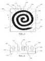
- FIG. 1is a top plan view of a substrate having a groove in accordance with the present invention.
- FIG. 2is a side sectional view of the substrate of FIG. 1 taken along the line A-A.
- FIG. 3is a top plan view of the substrate of FIG. 1 having a pad.
- FIG. 4is a side sectional view of the substrate of FIG. 3 taken along the line B-B.
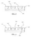
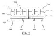
- FIGS. 5-7are side sectional views of alternative embodiments of the substrate and pad of FIG. 3 .
- FIG. 8is a top plan view of the substrate and pad of FIG. 3 with a bonding material.
- FIG. 9is a side sectional view of the substrate and bonding material of FIG. 8 taken along the line C-C.
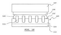
- FIG. 10is a side sectional view of the substrate, pad, and bonding material of FIG. 8 attached to a second component.
- FIG. 11is a top plan view of an alternative embodiment of a substrate having a pad.
- FIG. 12is a top plan view of the pad of FIG. 3 shown positioned within a boundary.
- FIGS. 13 and 14are top plan views of alternative embodiments of a substrate having a pad in accordance with the present invention.
- FIG. 15is a top perspective view of a substrate having a pad electrically connected with a chip in accordance with the present invention.
- FIG. 16is a side sectional view of the substrate of FIG. 15 taken along the line E-E.
- FIG. 17is a side sectional view of an alternative embodiment of the substrate and pad of FIG. 15 .
- FIG. 18is a side sectional view of the substrate and pad of FIG. 17 with a bonding material.
- FIG. 19is a top perspective view of a mandrel having a pad formed thereon in accordance with the present invention.
- FIG. 20is a side sectional view of the mandrel and pad of FIG. 15 taken along the line F-F.
- FIGS. 21 and 22are side sectional views showing the pad of FIG. 19 being embedded into a dielectric region.
- FIG. 23is a schematic depiction of a system according to one embodiment of the invention.
- an electrically conductive elementis “exposed at” a surface of a dielectric element indicates that the electrically conductive element is available for contact with a theoretical point moving in a direction perpendicular to the surface of the dielectric element toward the surface of the dielectric element from outside the dielectric element.
- a terminal or other conductive element which is exposed at a surface of a dielectric elementmay project from such surface; may be flush with such surface; or may be recessed relative to such surface and exposed through a hole or depression in the dielectric.
- Assembly 100includes a first component 105 as shown, for example, in FIGS. 1 and 2 .
- the componentincludes at least a dielectric region 120 and may also include a supporting element, e.g., a substrate, underlying the dielectric region 120 .
- the first componentmay be, for example, a dielectric element to be fabricated into a chip carrier, other component of a package, or a circuit panel.
- Substrate 110can be an additional dielectric layer of the component 105 or can be other structure, as described further below. As seen in FIGS. 1-2 .
- a continuous groove 124 having a floor 126is formed extending along the surface 122 of the dielectric region.
- Floor 126is defined as the lowest portion of groove 124 .
- At least a portion of groove 124extends in a curved path with respect to surface 122 .
- Groove 124can be formed by removing a portion of dielectric region 120 , which in one example can be done by laser ablation by directing a laser at surface 122 .
- a systeme.g., a computer, can be used to move an illumination spot produced by the laser to different locations of surface 122 .
- the laserablates or otherwise removes a portion of a sacrificial layer (if present) and a portion of dielectric region 120 .
- Groove 124is depicted with floor 126 being curved or rounded, though other cross-sections, such as rectangular, may be formed either purposefully or as a result of the constraints of using a laser.
- the sacrificial layermay be provided overlying surface 122 of dielectric region 120 prior to the step of ablating with the laser.
- the sacrificial layertypically can be a polymeric material and has an exposed surface that conforms to a contour of surface 122 .
- the sacrificial layercan be applied by spray-coating, spin-coating, dipping, or other method.
- the sacrificial layeris removable by chemical means, such as by using an etchant.
- the sacrificial layeris removable by peeling. While a sacrificial layer can be used, formation of groove 124 does not require the use of a sacrificial layer.
- a conductive elementis formed which extends in a direction of the groove along surface 122 .
- catalyst layercan be formed overlying the exposed portions of dielectric region 120 and/or the sacrificial layer, if present.
- the catalyst layeroverlies at least floor 126 of groove 124 and is typically comprised of a thin layer of metal particles which can catalyze a subsequent metal deposition process, for example, a subsequent aqueous deposition process used in plating metal layers thereon.
- the catalyst layercan include platinum particles.
- the catalyst layercan be formed by providing a liquid containing the catalyst particles to the exposed surfaces of the sacrificial layer, for example, by dipping the substrate in a bath containing the catalyst particles.
- the catalyst layertypically uniformly coats first component 105 .
- the sacrificial layerif present, is removed from first component 105 , thereby also removing the catalyst layer disposed on the sacrificial layer. In this way, after the sacrificial layer has been removed the catalyst layer is disposed only in groove 124 . If no sacrificial layer is present, the catalyst layer can be deposited only in or along areas of first component 105 that are to be plated to form a conductive element, which, for example, can be only the area in groove 124 .
- a seed layercan then be selectively deposited onto the catalyst layer, and the process can continue with the deposition of one or more metal layers, which can include any of or all of an adhesion layer, a barrier metal layer, and a primary metal layer.
- metal layerscan include any of or all of an adhesion layer, a barrier metal layer, and a primary metal layer.
- seed layer, adhesion layer, barrier metal layer or primary metal layeris deposited by plating.
- the result of this process of selectively depositing a metal onto an area where the catalyst layer is presentis the formation of a conductive element 132 , as seen in FIGS. 3 and 4 , formed in groove 124 . Shown more clearly in FIG.
- cross-sectional dimensions of conductive element 134i.e., a width and a height or thickness of conductive element 132 above floor 126 of groove 124 , are at least partly defined by the groove 124 .
- Conductive element 132is depicted as having a planar top surface 135 , although in practice, some degree of a “U” shaped surface may occur. The height of conductive element 132 may thusly be defined as extending from its lowest point (i.e., the lowest point of groove 124 ) to its highest point.
- Corresponding cross-sectional dimensions of a depth 128 and a width 130 of groove 124aid in defining conductive element 132 .
- Depth 128is measured between floor 126 and surface 122 of dielectric region 120 .
- the depthcan be greater than the width 130 of the groove, as measured in a perpendicular direction along surface 122 , being perpendicular to the depth 128 and a lengthwise direction 125 of the groove 124 .
- depth 128may be greater than a width of conductive element 132 , which corresponds to width 130 .
- conductive element 132can have a contour which conforms to the inner surface of groove 124 and is at least partially embedded within groove 124 in dielectric region 120 .
- the height of conductive element 132can be at least substantially the same throughout the path of the conductive element along the segments thereof.
- the sacrificial layercan be removed after one or more of the metal layers is deposited which make up conductive element 132 .
- the sacrificial layercan be removed after depositing any or all of a seed layer, an adhesion layer, a barrier metal layer or other metal layer provided before the primary metal layer is deposited.
- the sacrificial layermay be removed in a “lift-off” process from the dielectric region, such as by etching, peeling or other method. Then, after removing the sacrificial layer, the metal deposition can continue with the deposition of one or more subsequent metal layers including the primary metal layer to form conductive element 132 .
- Conductive element 132forms a pad 134 exposed at surface 122 of dielectric region 120 .
- Pad 134can be connected to or be formed integrally with one or more other conductive elements (not shown) such as a conductive trace, other conductive pad, or other circuit component.
- Such other conductive elementcan extend from or be connected to one or more locations of conductive element 134 , such as end 139 or path location 141 .
- Pad 134permits electrical interconnection of first component 105 with a second component 107 , shown in FIG. 10 .
- Pad 134is defined by conductive element 132 , which has cross-sectional dimensions and a path at least partly defined by the path of groove 124 .
- Conductive element 132extends from floor 126 of groove 124 to a height above floor 126 . As shown in FIG. 4 , the height of conductive element 132 is greater than a distance between floor 126 and surface 122 . However, in alternative embodiments of the present invention shown in FIGS. 5 and 6 , the height of the conductive element above the floor can be equal to or less than such distance, respectively. In FIG.
- a conductive element 232extends to a height above a floor 226 equal to the distance between floor 226 and a surface 222 of a dielectric region 220 .
- top surface 244 of conductive element 232can be co-planar with surface 222 of the dielectric region.
- FIG. 6shows a conductive element 332 extending to a height above a floor 326 less than the distance between floor 326 and a surface 322 of a dielectric region 320 . Such that a top surface 344 of the conductive element is disposed below the surface 322 of the dielectric region.
- conductive element 132includes at least two adjacent segments 136 , 138 that are separated by a portion 137 of dielectric region 120 . Accordingly, it can be said that a theoretical straight line 199 intersects at least three segments 136 , 138 , and 150 of conductive element 132 .
- Conductive element 132 in its entiretyhas a length along surface 122 that is at least ten times greater than its height 133 , e.g., as, measured from floor 126 to top surface 135 .
- Pad 134can be constructed such that conductive element 132 occupies less than about seventy-five percent of an area of surface 122 of dielectric region 120 within a generally circular-shaped boundary 146 , shown in FIG.
- a conductive element according to the present inventionoccupies ten to seventy-five percent of an area within such boundary, and in certain embodiments, a conductive element can occupy about twenty-five percent of an area within such boundary.
- First component 105is shown and described in one configuration, although other configurations of assembly 100 and first component 105 may be realized by the present invention and will be described more thoroughly below.
- first component 105includes conductive element 132 that has a spiral path (as shown in FIGS. 1 and 3 ).
- a first component 505can include a conductive element 532 having a sinusoidal path on a surface 522 (as shown in FIG. 13 ), or a first component 605 can include a conductive element 632 having an oscillating path on a surface 622 (as shown in FIG. 14 ).
- a sinusoidal pathis generally wave-shaped, and an oscillating path is one that generally extends in a side-to-side manner along the direction from the beginning to the end of the conductive element.
- An “oscillating path”broadly describes an array of configurations of a conductive element, including a sinusoidal path. Moreover, an oscillating path need not be uniform as shown in FIG. 14 .
- Conductive element 632may form an oscillating path that forms a portion of a pad, with one or more portions being configured in other manners.
- a padmay include a portion that forms an oscillating path and another portion that crosses the oscillating path but cannot be characterized by any particular type of shape.
- An oscillating pathcan, for instance, be a triangular wave shape, a zig-zag pattern, or any other similar pattern. It is not necessary that the oscillating path have segments 636 of uniform length or that the path reverse direction with the same angle 634 between segments. At least some adjacent segments of the path may not be joined together at both ends thereof. Rather, in some cases, the conductive element can have an oscillating path which “meanders” within a defined area set for a conductive pad, in which segments of the path can be of varying length and can have varying angles between segments.
- conductive elements 532 and 632each may occupy less than about seventy-five percent of an area of their respective surface 522 , 622 within a generally square-shaped boundary defined in general by the outermost edges of conductive elements 532 and 632 , respectively.
- any other desired shape or configuration of a conductive elementmay be realized to form a pad.
- One advantage of the present inventionis the ability to define a general outer boundary of a pad with any pattern of a conductive element disposed within said boundary.
- the conductive elementdoes not require a precise pattern, but is effective due to its overall structure as a pad.
- Conductive element 132does not overlap or cross itself along its path.
- a conductive element 432 of a first component 405may overlap or cross itself in one or more areas on a surface 422 .
- a conductive materialcan be deposited overlying surface 122 of dielectric region 120 and at least a portion of groove 124 . Certain of the conductive material overlying at least a portion of surface 122 can then be removed to expose surface 122 of dielectric region 120 .
- an electrically conductive bonding material 140can be deposited at least partly overlying pad 134 , as shown in FIGS. 8 and 9 .
- the electrically conductive bonding material 140which preferably has a melting temperature below 300° C. and may be a solder material, can extend at least between outermost edges of pad 134 so as to entirely cover pad 134 when viewed from a direction normal to surface 122 , as shown in FIG. 8 .
- the electrically conductive bonding material 140is joined to conductive pad 134 to bridge portion 137 of dielectric region 120 between segments 136 , 138 of conductive element 132 , shown more clearly in FIG. 3 .
- Second component 107shown in FIG.
- bonding material 140can be applied directly to pad 132 prior to assembling first component 105 with second component 107 , bonding material 140 can alternately be applied only to the terminal 108 of the second component 107 or can be applied separately to each of the pad 132 and the terminal 108 before assembling the components together.
- conductive element 132includes an exposed top surface 144 exposed above surface 122 of dielectric region 120 and exposed “vertical surfaces” 142 extending between top surface 144 and surface 122 .
- “Vertical surfaces” 142are edge surfaces that extend away from top surface 144 , although they may or may not be in a vertical or normal direction with respect to the top surface 144 and dielectric region surface 122 .
- Bonding material 140is in contact with top surface 144 and vertical surfaces 142 . In alternate embodiments, such as those depicted in FIGS. 5 and 6 , the bonding material contacts the conductive element and surface in a different manner. In FIG.
- a top surface 244is essentially flush with surface 222 of dielectric region 220 .
- the bonding materialwould have an essentially planar contact surface with the top surfaces 244 of conductive element 232 and surface 222 .
- the bonding materialalso contacts vertical surfaces 348 of groove 324 exposed between top surface 344 of conductive element 332 and surface 322 of dielectric region 320 .
- a surface layer including nickel, gold, or another metalcan be plated or otherwise exposed at one or more surface of pad 134 , such as at the top and edge surfaces 142 , 144 .
- embodiments of the first componentcan be comprised of a single dielectric region, can include a substrate underlying a dielectric region, or can comprise more than one dielectric regions or layers in a stacked formation.
- the dielectric regioncan comprise two or more stacked layers of dielectric materials, with at least two adjacent layers thereof including different materials.
- the dielectric regiontypically includes one or more dielectric materials such as silicon dioxide in any form, other dielectric compound of silicon, a polymeric material, or other inorganic dielectric material, such as a ceramic material, among others.
- a substrate according to the present inventiontypically consists essentially of a monocrystalline semiconductor material such as, for example, silicon, an alloy of silicon with another material, one or more III-V semiconductor compounds such as gallium arsenide among others, or one or more II-VI semiconductor compounds.
- the substratecan be a silicon-on-insulator substrate which includes a buried oxide (“BOX”) layer that separates an active semiconductor device layer at a front face from a bulk semiconductor region at a rear face.
- BOXburied oxide
- substrate 110includes an opening 116 extending between the rear face 112 and front face 114 , and a plurality of conductive elements 118 disposed at front face 114 .
- Conductive element 132electrically connects pad 134 to at least one of conductive elements 118 by extending through opening 116 in substrate 110 and an adjacent opening in dielectric region 120 .
- At least a portion of groove 124can extend along an interior surface of opening 116 , and conductive element 132 can extend within the portion of groove 124 .
- FIGS. 15-18Another embodiment of a first component 705 is shown in FIGS. 15-18 , and includes a chip 710 and a passivation layer 703 overlying an upper surface of chip 710 .
- a bond pad 750is disposed on an exposed surface 704 of passivation layer 703 , which is a dielectric region having an exposed surface.
- a conductive pad 734is also formed on surface 704 in a manner as described above.
- a trace 752is electrically connected with chip 710 and extends along surface 704 to electrically connect with a portion of pad 734 . Trace 752 may be formed in conjunction with pad 734 during a process as outlined above, or may be formed to electrically connect chip 710 with pad 734 after pad 734 has been formed.
- a plurality of tracescan also or alternatively be positioned in the position where trace 752 is disposed, as shown in FIG. 15 .
- Pad 734allows for electrical connection between chip 710 and an external component that can be joined thereto as described above with reference to FIG. 10 , for example.
- a solder mask 756may be deposited overlying passivation layer 703 and trace 752 , such as by using a photolithographic method.
- Pad 132is thusly left exposed and may be covered by an electrically conductive bonding material 740 ( FIG. 18 ).
- Another componentmay then be electrically connected to chip 710 through the bonding material 740 in a manner similar to that depicted in FIG. 10 .
- a second component having a terminal with bonding material thereoncan be joined to pad 734 to form the electrical connection.
- FIGS. 19-22shows another method of forming a first component 805 in accordance with the present invention.
- a conductive pad 834( FIGS. 19-20 ) is formed on a planar surface 862 of a mandrel 860 or other type of lead frame.
- Pad 834is formed as a plated conductive element in a similar configuration as discussed above.
- Mandrel 860is then positioned adjacent a dielectric region 820 such that pad 834 is adjacent a surface 822 of dielectric region 820 ( FIG. 21 ). Force is applied to mandrel 860 to embed pad 834 into dielectric region 820 , which may be at least partially cured.
- Mandrel 860is then removed, with the resulting first component 805 ( FIG. 22 ) being similar to those in the above-described embodiments.
- mandrel 860may be comprised of one or more metal sheets, and the step of removing mandrel 860 is conducted by etching away each metal sheet to expose the pad 834 .
- dielectric region 820may not be pre-formed, but rather, a dielectric material may be deposited onto surface 862 of mandrel 860 , and then mandrel 860 removed to form first component 805 .
- a first component having a spiral or oscillating path conductive pad as described above, or formed according to a technique described abovecan be joined or electrically connected to a second component with an electrically conductive bonding material contacting surfaces of the conductive pad in a manner as described above, and contacting a terminal of the second component.
- the bonding materialbridges the portion of the surface of the dielectric region between the at least two adjacent segments of the conductive pad.
- the bonding materialcan be applied to such conductive pad before assembling the first component with the second component, in which case the bonding material on the conductive pad will form part of the joint or electrically conductive connection between the first and second components.
- the bonding materialcan be applied to a terminal of the second component and not applied to such conductive pad.
- the bonding material from the terminal of the second componentwill flow onto surfaces of the conductive pad and will then bridge the portion of the surface of the dielectric region between the at least two adjacent segments.
- an electrically conductive jointcan be formed by heating a bond metal such as solder to a temperature sufficient to cause the bond metal to flow, the bond metal then contacting surfaces of such pad and a terminal of the second component juxtaposed therewith. The bond metal then re-solidifies again to form the electrically conductive joint.
- a bonding materialcan be applied separately to such conductive pad and to a terminal of a second component, after which the first and second components can be brought together and joined as described above.
- a first component according to the present inventioncan be a microelectronic element having a plurality of active semiconductor devices adjacent the surface of the dielectric region.
- the first componentcan be a microelectronic element having a plurality of contacts at its surface, and can further include a trace electrically connecting the conductive pad with at least one of the plurality of contacts.
- the first componentcan be a microelectronic element having a plurality of contacts at surface, and the conductive pad can be electrically connected with at least one of the plurality of contacts.
- a substrateconsists essentially of monocrystalline semiconductor material, and a dielectric region overlying the substrate includes a layer of dielectric material conforming to a contour of a sloped surface of the substrate.
- the substratemay consist essentially of dielectric material, or may include a region consisting essentially of conductive material with a dielectric region overlying the region of conductive material.
- the embodiments described abovecan include grooves and apertures formed such as by a direct writing method, e.g., using a laser to define a path.
- a direct writing methode.g., using a laser to define a path.
- other methodscan be used to form such features according to the present invention.
- Mechanical millingcan be utilized, wherein a small diameter element, which can be referred to as a hammer, repeatedly strikes the sacrificial layer, if present, and the dielectric region to loosen and remove such material to form a groove or aperture.
- Another method that can be utilizedis a sandblasting technique together with a metal stencil, which is positioned to overlie sacrificial layer and/or dielectric region and includes openings that are shaped in accordance with a desired final pattern of the conductive elements.
- a sandblasting techniqueis employed by directing a sand-based material at the dielectric region in a direction such that the sand-based material will strike the sacrificial layer and/or the dielectric region in the areas exposed through the openings. One or more grooves are thereby formed in the dielectric region.
- These particular techniques of mechanical milling and sand-blastingcan be considered “non-photolithographic techniques” because they do not rely primarily on patterning using exposure of a photoresist through a photomask. Description of such patterning techniques and other structures which can be formed therewith is found in commonly owned U.S. application Ser. No. 12/842,669 filed Jul. 23, 2010, the disclosure of which is incorporated by reference herein. The remaining steps of the method of constructing a structure in accordance with the present invention are as set forth above.
- the methods herein disclosedcan achieve a top surface of a pad having greater planarity than those formed by existing methods, such as rastering.
- the pads according to the present inventiontypically include segments separated by gaps, the planarity of the top surface can be achieved by top surfaces of adjacent segments being co-planar or substantially defining a single plane.
- sacrificial layercertain methods of removing sacrificial layer require the sacrificial layer to be more brittle in nature. For instance, the sandblasting technique described above is more effectively carried out with a more brittle sacrificial layer, so that the sand-based material does not become embedded in the sacrificial layer rather than breaking and removing same.
- the resulting assembliescan be or include a microelectronic unit having active circuit elements, e.g., transistors, diodes, or other microelectronic or microelectromechanical devices therein, among others, and can have traces which are formed by one or more of the techniques, e.g., even non-photolithographic techniques, as described above.
- the resulting assembliescan be or include an interposer structure having a substrate of at least one of semiconductor or dielectric material which has traces formed as described above but which does not have active circuit elements therein.
- An interposer structure or component in accordance such embodimentscan have conductive elements exposed at one or more of the front and rear faces for interconnection with one or more external components such as, for example, a microelectronic element, substrate or circuit panel.
- the resulting assembliescan be or include a microelectronic unit having active circuit elements, e.g., transistors, diodes, or other microelectronic or microelectromechanical devices therein, among others, and have traces formed by one or more of the methods described above.
- the resulting assembliescan be or include an interposer structure having a substrate of at least one of semiconductor or dielectric material which has traces formed by one or more of the above-described methods, but which does not have active circuit elements therein.
- An interposer structure or component in accordance such embodimentscan have conductive elements exposed at one or more of the front and rear faces for interconnection with one or more external components such as, for example, a microelectronic element, substrate or circuit panel.
- a system 900 in accordance with a further embodiment of the inventionincludes a structure 906 as described above in conjunction with other electronic components 908 and 910 .
- component 908is a semiconductor chip whereas component 910 is a display screen, but any other components can be used.
- the structure 906 as described abovemay be, for example, a composite chip or a structure incorporating plural chips. In a further variant, both may be provided, and any number of such structures may be used.
- Structure 906 and components 908 and 910are mounted in a common housing 901 , schematically depicted in broken lines, and are electrically interconnected with one another as necessary to form the desired circuit.
- the systemincludes a circuit panel 902 such as a flexible printed circuit board, and the circuit panel includes numerous conductors 904 , of which only one is depicted in FIG. 23 , interconnecting the components with one another.
- the housing 901is depicted as a portable housing of the type usable, for example, in a cellular telephone or personal digital assistant, and screen 910 is exposed at the surface of the housing.
- structure 906includes a light-sensitive element such as an imaging chip
- a lens 911 or other optical devicealso may be provided for routing light to the structure.
- the simplified system shown in FIG. 23is merely exemplary; other systems, including systems commonly regarded as fixed structures, such as desktop computers, routers and the like can be made using the structures discussed above.
Landscapes
- Engineering & Computer Science (AREA)
- Computer Hardware Design (AREA)
- Microelectronics & Electronic Packaging (AREA)
- Power Engineering (AREA)
- Physics & Mathematics (AREA)
- General Physics & Mathematics (AREA)
- Geometry (AREA)
- Condensed Matter Physics & Semiconductors (AREA)
- Manufacturing & Machinery (AREA)
- Internal Circuitry In Semiconductor Integrated Circuit Devices (AREA)
- Structures For Mounting Electric Components On Printed Circuit Boards (AREA)
- Electric Connection Of Electric Components To Printed Circuits (AREA)
- Wire Bonding (AREA)
- Piezo-Electric Or Mechanical Vibrators, Or Delay Or Filter Circuits (AREA)
- Coils Or Transformers For Communication (AREA)
- Micromachines (AREA)
Abstract
Description
Claims (26)
Priority Applications (1)
| Application Number | Priority Date | Filing Date | Title |
|---|---|---|---|
| US13/589,359US8772908B2 (en) | 2010-11-15 | 2012-08-20 | Conductive pads defined by embedded traces |
Applications Claiming Priority (4)
| Application Number | Priority Date | Filing Date | Title |
|---|---|---|---|
| KR10-2010-0113272 | 2010-11-15 | ||
| KR1020100113272AKR101059490B1 (en) | 2010-11-15 | 2010-11-15 | Conductive pads constructed by embedded traces |
| US12/963,938US8432045B2 (en) | 2010-11-15 | 2010-12-09 | Conductive pads defined by embedded traces |
| US13/589,359US8772908B2 (en) | 2010-11-15 | 2012-08-20 | Conductive pads defined by embedded traces |
Related Parent Applications (1)
| Application Number | Title | Priority Date | Filing Date |
|---|---|---|---|
| US12/963,938ContinuationUS8432045B2 (en) | 2010-11-15 | 2010-12-09 | Conductive pads defined by embedded traces |
Publications (2)
| Publication Number | Publication Date |
|---|---|
| US20120306092A1 US20120306092A1 (en) | 2012-12-06 |
| US8772908B2true US8772908B2 (en) | 2014-07-08 |
Family
ID=44933774
Family Applications (2)
| Application Number | Title | Priority Date | Filing Date |
|---|---|---|---|
| US12/963,938Expired - Fee RelatedUS8432045B2 (en) | 2010-11-15 | 2010-12-09 | Conductive pads defined by embedded traces |
| US13/589,359ActiveUS8772908B2 (en) | 2010-11-15 | 2012-08-20 | Conductive pads defined by embedded traces |
Family Applications Before (1)
| Application Number | Title | Priority Date | Filing Date |
|---|---|---|---|
| US12/963,938Expired - Fee RelatedUS8432045B2 (en) | 2010-11-15 | 2010-12-09 | Conductive pads defined by embedded traces |
Country Status (6)
| Country | Link |
|---|---|
| US (2) | US8432045B2 (en) |
| JP (1) | JP2014503992A (en) |
| KR (1) | KR101059490B1 (en) |
| CN (1) | CN103299419B (en) |
| TW (2) | TWI401781B (en) |
| WO (1) | WO2012067992A2 (en) |
Cited By (2)
| Publication number | Priority date | Publication date | Assignee | Title |
|---|---|---|---|---|
| US20120146273A1 (en)* | 2009-04-22 | 2012-06-14 | Tiefenboeck Herbert | Receiving device for receiving semiconductor substrates |
| US10958006B2 (en) | 2016-06-02 | 2021-03-23 | Te Connectivity Germany Gmbh | Contact element and method for production thereof |
Families Citing this family (5)
| Publication number | Priority date | Publication date | Assignee | Title |
|---|---|---|---|---|
| WO2016159245A1 (en)* | 2015-03-31 | 2016-10-06 | 株式会社NejiLaw | Conduction-path-equipped member, method for patterning conduction path, and method for measuring changes in member |
| US9653419B2 (en) | 2015-04-08 | 2017-05-16 | Intel Corporation | Microelectronic substrate having embedded trace layers with integral attachment structures |
| CN104752443B (en)* | 2015-04-20 | 2016-03-02 | 京东方科技集团股份有限公司 | Substrate support plate, flexible display panels and corresponding manufacture method, flexible display apparatus |
| US10080290B2 (en)* | 2015-11-17 | 2018-09-18 | Intel Corporation | Stretchable embedded electronic package |
| TWI736093B (en) | 2019-12-31 | 2021-08-11 | 財團法人工業技術研究院 | Package structure |
Citations (129)
| Publication number | Priority date | Publication date | Assignee | Title |
|---|---|---|---|---|
| US4682074A (en) | 1984-11-28 | 1987-07-21 | U.S. Philips Corporation | Electron-beam device and semiconductor device for use in such an electron-beam device |
| US4765864A (en) | 1987-07-15 | 1988-08-23 | Sri International | Etching method for producing an electrochemical cell in a crystalline substrate |
| US5481133A (en) | 1994-03-21 | 1996-01-02 | United Microelectronics Corporation | Three-dimensional multichip package |
| US5686762A (en) | 1995-12-21 | 1997-11-11 | Micron Technology, Inc. | Semiconductor device with improved bond pads |
| US5700735A (en) | 1996-08-22 | 1997-12-23 | Taiwan Semiconductor Manufacturing Company, Ltd. | Method of forming bond pad structure for the via plug process |
| US5703408A (en) | 1995-04-10 | 1997-12-30 | United Microelectronics Corporation | Bonding pad structure and method thereof |
| US5808874A (en) | 1996-05-02 | 1998-09-15 | Tessera, Inc. | Microelectronic connections with liquid conductive elements |
| EP0926723A1 (en) | 1997-11-26 | 1999-06-30 | STMicroelectronics S.r.l. | Process for forming front-back through contacts in micro-integrated electronic devices |
| US6002161A (en)* | 1995-12-27 | 1999-12-14 | Nec Corporation | Semiconductor device having inductor element made of first conductive layer of spiral configuration electrically connected to second conductive layer of insular configuration |
| US6005466A (en) | 1994-07-29 | 1999-12-21 | Mitel Semiconductor Limited | Trimmable inductor structure |
| KR19990088037A (en) | 1998-05-04 | 1999-12-27 | 루센트 테크놀러지스 인크 | Bond pad design for integrated circuits |
| US6013948A (en) | 1995-11-27 | 2000-01-11 | Micron Technology, Inc. | Stackable chip scale semiconductor package with mating contacts on opposed surfaces |
| US6022758A (en) | 1994-07-10 | 2000-02-08 | Shellcase Ltd. | Process for manufacturing solder leads on a semiconductor device package |
| US6031274A (en) | 1996-10-11 | 2000-02-29 | Hamamatsu Photonics K.K. | Back irradiation type light-receiving device and method of making the same |
| US6103552A (en) | 1998-08-10 | 2000-08-15 | Lin; Mou-Shiung | Wafer scale packaging scheme |
| US6143369A (en) | 1996-01-12 | 2000-11-07 | Matsushita Electric Works, Ltd. | Process of impregnating substrate and impregnated substrate |
| US6143396A (en) | 1997-05-01 | 2000-11-07 | Texas Instruments Incorporated | System and method for reinforcing a bond pad |
| US6169319B1 (en) | 1999-08-12 | 2001-01-02 | Tower Semiconductor Ltd. | Backside illuminated image sensor |
| US6181016B1 (en)* | 1999-06-08 | 2001-01-30 | Winbond Electronics Corp | Bond-pad with a single anchoring structure |
| US6261865B1 (en) | 1998-10-06 | 2001-07-17 | Micron Technology, Inc. | Multi chip semiconductor package and method of construction |
| JP2001217386A (en) | 2000-02-03 | 2001-08-10 | Seiko Epson Corp | Semiconductor device, method of manufacturing the same, and electronic device |
| US6277669B1 (en) | 1999-09-15 | 2001-08-21 | Industrial Technology Research Institute | Wafer level packaging method and packages formed |
| US20010028098A1 (en)* | 1998-08-07 | 2001-10-11 | Ping Liou | Method and structure of manufacturing a high-q inductor with an air trench |
| US6313540B1 (en) | 1998-12-25 | 2001-11-06 | Nec Corporation | Electrode structure of semiconductor element |
| US20010048591A1 (en) | 1997-11-25 | 2001-12-06 | Joseph Fjelstad | Microelectronics component with rigid interposer |
| US6368410B1 (en) | 1999-06-28 | 2002-04-09 | General Electric Company | Semiconductor processing article |
| US20020048668A1 (en)* | 1997-09-13 | 2002-04-25 | Kabushiki Kaisha Toshiba | Ferrite magnetic film structure having magnetic anisotropy, method of manufacturing the same, and planar magnetic device employing ferrite magnetic film structure having magnetic anisotropy |
| US20020061723A1 (en) | 2000-11-17 | 2002-05-23 | Duescher Wayne O. | Raised island abrasive and process of manufacture |
| US20020109236A1 (en) | 2001-02-09 | 2002-08-15 | Samsung Electronics Co., Ltd. | Three-dimensional multi-chip package having chip selection pads and manufacturing method thereof |
| US6472247B1 (en) | 2000-06-26 | 2002-10-29 | Ricoh Company, Ltd. | Solid-state imaging device and method of production of the same |
| US6492201B1 (en) | 1998-07-10 | 2002-12-10 | Tessera, Inc. | Forming microelectronic connection components by electrophoretic deposition |
| US6498387B1 (en) | 2000-02-15 | 2002-12-24 | Wen-Ken Yang | Wafer level package and the process of the same |
| US20030059976A1 (en) | 2001-09-24 | 2003-03-27 | Nathan Richard J. | Integrated package and methods for making same |
| WO2003025998A2 (en) | 2001-09-14 | 2003-03-27 | Motorola, Inc. | Method of forming a bond pad and structure thereof |
| US6555913B1 (en)* | 1998-07-17 | 2003-04-29 | Murata Manufacturing Co., Ltd. | Electronic component having a coil conductor with photosensitive conductive paste |
| US6586955B2 (en) | 2000-03-13 | 2003-07-01 | Tessera, Inc. | Methods and structures for electronic probing arrays |
| US6608377B2 (en) | 2001-01-30 | 2003-08-19 | Samsung Electronics Co., Ltd. | Wafer level package including ground metal layer |
| US20040016942A1 (en) | 2002-04-24 | 2004-01-29 | Seiko Epson Corporation | Semiconductor device and a method of manufacturing the same, a circuit board and an electronic apparatus |
| US6693358B2 (en) | 2000-10-23 | 2004-02-17 | Matsushita Electric Industrial Co., Ltd. | Semiconductor chip, wiring board and manufacturing process thereof as well as semiconductor device |
| US20040043607A1 (en) | 2002-08-29 | 2004-03-04 | Farnworth Warren M. | Methods for creating electrophoretically insulated vias in semiconductive substrates and resulting structures |
| US6727576B2 (en) | 2001-10-31 | 2004-04-27 | Infineon Technologies Ag | Transfer wafer level packaging |
| TW200406884A (en) | 2002-10-30 | 2004-05-01 | Intelligent Sources Dev Corp | Method of forming a stacked-gate cell structure and its NAND-type flash memory array |
| US6737300B2 (en) | 2001-01-24 | 2004-05-18 | Advanced Semiconductor Engineering, Inc. | Chip scale package and manufacturing method |
| US6743660B2 (en) | 2002-01-12 | 2004-06-01 | Taiwan Semiconductor Manufacturing Co., Ltd | Method of making a wafer level chip scale package |
| US20040104454A1 (en) | 2002-10-10 | 2004-06-03 | Rohm Co., Ltd. | Semiconductor device and method of producing the same |
| US20040155354A1 (en) | 2000-06-02 | 2004-08-12 | Seiko Epson Corporation | Semiconductor device, method of fabricating the same, stack-type semiconductor device, circuit board and electronic instrument |
| US20040178495A1 (en) | 2003-03-14 | 2004-09-16 | Yean Tay Wuu | Microelectronic devices and methods for packaging microelectronic devices |
| US20040188819A1 (en) | 2003-03-31 | 2004-09-30 | Farnworth Warren M. | Wafer level methods for fabricating multi-dice chip scale semiconductor components |
| US20040188822A1 (en) | 2003-01-15 | 2004-09-30 | Kazumi Hara | Semiconductor chip, semiconductor wafer, semiconductor device and method of manufacturing the same, circuit board, and electronic instrument |
| US6812549B2 (en) | 2001-03-07 | 2004-11-02 | Seiko Epson Corporation | Wiring board and fabricating method thereof, semiconductor device and fabricating method thereof, circuit board and electronic instrument |
| US20040217483A1 (en) | 2003-04-30 | 2004-11-04 | Infineon Technologies Ag | Semiconductor device and method for fabricating the semiconductor device |
| US20040222508A1 (en) | 2003-03-18 | 2004-11-11 | Akiyoshi Aoyagi | Semiconductor device, electronic device, electronic apparatus, method of manufacturing semiconductor device, and method of manufacturing electronic device |
| EP1482553A2 (en) | 2003-05-26 | 2004-12-01 | Sanyo Electric Co., Ltd. | Semiconductor device and manufacturing method thereof |
| US6828175B2 (en) | 2002-08-29 | 2004-12-07 | Micron Technology, Inc. | Semiconductor component with backside contacts and method of fabrication |
| US20040251525A1 (en) | 2003-06-16 | 2004-12-16 | Shellcase Ltd. | Methods and apparatus for packaging integrated circuit devices |
| WO2004114397A1 (en) | 2003-06-20 | 2004-12-29 | Koninklijke Philips Electronics N.V. | Electronic device, assembly and methods of manufacturing an electronic device |
| US20050012225A1 (en) | 2002-11-15 | 2005-01-20 | Choi Seung-Yong | Wafer-level chip scale package and method for fabricating and using the same |
| US20050046002A1 (en) | 2003-08-26 | 2005-03-03 | Kang-Wook Lee | Chip stack package and manufacturing method thereof |
| US6864172B2 (en) | 2002-06-18 | 2005-03-08 | Sanyo Electric Co., Ltd. | Manufacturing method of semiconductor device |
| US6867123B2 (en) | 2001-02-08 | 2005-03-15 | Renesas Technology Corp. | Semiconductor integrated circuit device and its manufacturing method |
| US20050056903A1 (en) | 2003-08-28 | 2005-03-17 | Satoshi Yamamoto | Semiconductor package and method of manufacturing same |
| EP1519410A1 (en) | 2003-09-25 | 2005-03-30 | Interuniversitair Microelektronica Centrum vzw ( IMEC) | Method for producing electrical through hole interconnects and devices made thereof |
| JP2005093486A (en) | 2003-09-12 | 2005-04-07 | Seiko Epson Corp | Semiconductor device manufacturing method and semiconductor device |
| US6879049B1 (en) | 1998-01-23 | 2005-04-12 | Rohm Co., Ltd. | Damascene interconnection and semiconductor device |
| US20050099259A1 (en)* | 2003-09-30 | 2005-05-12 | Harris Edward B. | Inductor formed in an integrated circuit |
| TW200522274A (en) | 2003-12-26 | 2005-07-01 | Intelligent Sources Dev Corp | Paired stack-gate flash cell structure and its contactless nand-type flash memory arrays |
| US20050148160A1 (en)* | 2002-03-06 | 2005-07-07 | Farnworth Warren M. | Encapsulated semiconductor components and methods of fabrication |
| US20050156330A1 (en) | 2004-01-21 | 2005-07-21 | Harris James M. | Through-wafer contact to bonding pad |
| TW200535435A (en) | 2004-03-29 | 2005-11-01 | Applied Materials Inc | High throughput measurement of via defects in interconnects |
| US20050260794A1 (en) | 2002-09-03 | 2005-11-24 | Industrial Technology Research Institute | Method for fabrication of wafer level package incorporating dual compliant layers |
| US20050279916A1 (en) | 2004-05-03 | 2005-12-22 | Tessera, Inc. | Image sensor package and fabrication method |
| US20050282374A1 (en) | 2004-06-22 | 2005-12-22 | Samsung Electronics Co., Ltd. | Method of forming a thin wafer stack for a wafer level package |
| US20050287783A1 (en) | 2004-06-29 | 2005-12-29 | Kirby Kyle K | Microelectronic devices and methods for forming interconnects in microelectronic devices |
| US6982475B1 (en) | 1998-03-20 | 2006-01-03 | Mcsp, Llc | Hermetic wafer scale integrated circuit structure |
| EP1619722A1 (en) | 2003-04-16 | 2006-01-25 | Hamamatsu Photonics K. K. | Method for manufacturing backside-illuminated optical sensor |
| US20060017161A1 (en) | 2004-07-22 | 2006-01-26 | Jae-Sik Chung | Semiconductor package having protective layer for re-routing lines and method of manufacturing the same |
| US20060046348A1 (en) | 2004-09-01 | 2006-03-02 | Kang Byoung Y | Semiconductor chip packages and methods for fabricating the same |
| US20060043598A1 (en) | 2004-08-31 | 2006-03-02 | Kirby Kyle K | Methods of manufacture of a via structure comprising a plurality of conductive elements, semiconductor die, multichip module, and system including same |
| US20060046471A1 (en) | 2004-08-27 | 2006-03-02 | Kirby Kyle K | Methods for forming vias of varying lateral dimensions and semiconductor components and assemblies including same |
| US20060068580A1 (en) | 2004-09-28 | 2006-03-30 | Sharp Kabushiki Kaisha | Semiconductor device and fabrication method thereof |
| US20060079019A1 (en) | 2004-10-08 | 2006-04-13 | Easetech Korea Co., Ltd. | Method for manufacturing wafer level chip scale package using redistribution substrate |
| EP1653510A2 (en) | 2004-10-28 | 2006-05-03 | Sanyo Electric Co., Ltd. | Semiconductor device and manufacturing method of the same |
| EP1653521A1 (en) | 2003-07-29 | 2006-05-03 | Hamamatsu Photonics K.K. | Backside-illuminated photodetector and method for manufacturing same |
| US20060094231A1 (en) | 2004-10-28 | 2006-05-04 | Lane Ralph L | Method of creating a tapered via using a receding mask and resulting structure |
| US20060115932A1 (en) | 1997-12-18 | 2006-06-01 | Farnworth Warren M | Method for fabricating semiconductor components with conductive vias |
| EP1686627A1 (en) | 2005-01-28 | 2006-08-02 | Samsung Electro-Mechanics Co., Ltd. | Semiconductor package and method of manufacturing the same |
| US20060175697A1 (en) | 2005-02-02 | 2006-08-10 | Tetsuya Kurosawa | Semiconductor device having semiconductor chips stacked and mounted thereon and manufacturing method thereof |
| US7091062B2 (en) | 2003-10-15 | 2006-08-15 | Infineon Technologies Ag | Wafer level packages for chips with sawn edge protection |
| US20060197217A1 (en) | 2005-03-02 | 2006-09-07 | Advanced Semiconductor Engineering, Inc. | Semiconductor package structure and method for manufacturing the same |
| US20060197216A1 (en) | 2005-03-02 | 2006-09-07 | Advanced Semiconductor Engineering, Inc. | Semiconductor package structure and method for manufacturing the same |
| US20060264029A1 (en) | 2005-05-23 | 2006-11-23 | Intel Corporation | Low inductance via structures |
| US20060292866A1 (en) | 2005-06-23 | 2006-12-28 | Borwick Robert L | Low temperature method for fabricating high-aspect ratio vias and devices fabricated by said method |
| JP2007053149A (en) | 2005-08-16 | 2007-03-01 | Renesas Technology Corp | Semiconductor wafer and its manufacturing method |
| US20070052050A1 (en) | 2005-09-07 | 2007-03-08 | Bart Dierickx | Backside thinned image sensor with integrated lens stack |
| JP2007157844A (en) | 2005-12-01 | 2007-06-21 | Sharp Corp | Semiconductor device and manufacturing method of semiconductor device |
| US7271033B2 (en) | 2001-12-31 | 2007-09-18 | Megica Corporation | Method for fabricating chip package |
| US20070269931A1 (en) | 2006-05-22 | 2007-11-22 | Samsung Electronics Co., Ltd. | Wafer level package and method of fabricating the same |
| US20080002460A1 (en) | 2006-03-01 | 2008-01-03 | Tessera, Inc. | Structure and method of making lidded chips |
| US20080020898A1 (en) | 2005-08-29 | 2008-01-24 | Johnson Health Tech Co., Ltd. | Rapid circuit training machine with dual resistance |
| JP2008091632A (en) | 2006-10-02 | 2008-04-17 | Manabu Bonshihara | Structure of external circuit connection section in semiconductor device and method of forming the same |
| US20080090333A1 (en) | 2006-10-17 | 2008-04-17 | Tessera, Inc. | Microelectronic packages fabricated at the wafer level and methods therefor |
| US20080116544A1 (en) | 2006-11-22 | 2008-05-22 | Tessera, Inc. | Packaged semiconductor chips with array |
| US20080157273A1 (en) | 2007-01-03 | 2008-07-03 | Stmicroelectronics Sa | Integrated electronic circuit chip comprising an inductor |
| US20080164574A1 (en) | 2006-12-06 | 2008-07-10 | Sergey Savastiouk | Integrated circuits with conductive features in through holes passing through other conductive features and through a semiconductor substrate |
| JP2008177249A (en) | 2007-01-16 | 2008-07-31 | Sharp Corp | Bonding pad for semiconductor integrated circuit, method for manufacturing the same, semiconductor integrated circuit, and electronic device |
| US7413929B2 (en) | 2001-12-31 | 2008-08-19 | Megica Corporation | Integrated chip package structure using organic substrate and method of manufacturing the same |
| US20080246136A1 (en) | 2007-03-05 | 2008-10-09 | Tessera, Inc. | Chips having rear contacts connected by through vias to front contacts |
| JP2008258258A (en) | 2007-04-02 | 2008-10-23 | Sanyo Electric Co Ltd | Semiconductor device |
| US7446036B1 (en) | 2007-12-18 | 2008-11-04 | International Business Machines Corporation | Gap free anchored conductor and dielectric structure and method for fabrication thereof |
| US20080284041A1 (en) | 2007-05-18 | 2008-11-20 | Samsung Electronics Co., Ltd. | Semiconductor package with through silicon via and related method of fabrication |
| US7456479B2 (en) | 2005-12-15 | 2008-11-25 | United Microelectronics Corp. | Method for fabricating a probing pad of an integrated circuit chip |
| US20090014843A1 (en) | 2007-06-06 | 2009-01-15 | Kawashita Michihiro | Manufacturing process and structure of through silicon via |
| US20090032966A1 (en) | 2007-08-01 | 2009-02-05 | Jong Ho Lee | Method of fabricating a 3-D device and device made thereby |
| US20090032951A1 (en) | 2007-08-02 | 2009-02-05 | International Business Machines Corporation | Small Area, Robust Silicon Via Structure and Process |
| US20090039491A1 (en) | 2007-08-10 | 2009-02-12 | Samsung Electronics Co., Ltd. | Semiconductor package having buried post in encapsulant and method of manufacturing the same |
| US20090065907A1 (en) | 2007-07-31 | 2009-03-12 | Tessera, Inc. | Semiconductor packaging process using through silicon vias |
| US20090085208A1 (en) | 2007-09-28 | 2009-04-02 | Nec Electronics Corporation | Semiconductor device |
| US20090212381A1 (en) | 2008-02-26 | 2009-08-27 | Tessera, Inc. | Wafer level packages for rear-face illuminated solid state image sensors |
| US20090263214A1 (en) | 2008-04-22 | 2009-10-22 | Taiwan Semiconductor Manufacturing Co., Ltd. | Fixture for p-through silicon via assembly |
| US20090309235A1 (en) | 2008-06-11 | 2009-12-17 | Stats Chippac, Ltd. | Method and Apparatus for Wafer Level Integration Using Tapered Vias |
| JP2010028601A (en) | 2008-07-23 | 2010-02-04 | Nippon Dempa Kogyo Co Ltd | Surface-mounted oscillator and electronic device with the oscillator packaged therein |
| US7719121B2 (en) | 2006-10-17 | 2010-05-18 | Tessera, Inc. | Microelectronic packages and methods therefor |
| US20100148371A1 (en) | 2008-12-12 | 2010-06-17 | Qualcomm Incorporated | Via First Plus Via Last Technique for IC Interconnects |
| US20100164062A1 (en) | 2008-12-31 | 2010-07-01 | Industrial Technology Research Institute | Method of manufacturing through-silicon-via and through-silicon-via structure |
| US7750487B2 (en) | 2004-08-11 | 2010-07-06 | Intel Corporation | Metal-metal bonding of compliant interconnect |
| US7767497B2 (en) | 2007-07-12 | 2010-08-03 | Tessera, Inc. | Microelectronic package element and method of fabricating thereof |
| KR20100087566A (en) | 2009-01-28 | 2010-08-05 | 삼성전자주식회사 | Method of forming the semiconductor device package |
| US7791199B2 (en) | 2006-11-22 | 2010-09-07 | Tessera, Inc. | Packaged semiconductor chips |
| US20120018894A1 (en) | 2010-07-23 | 2012-01-26 | Tessera Research Llc | Non-lithographic formation of three-dimensional conductive elements |
Family Cites Families (10)
| Publication number | Priority date | Publication date | Assignee | Title |
|---|---|---|---|---|
| JPS60160645A (en) | 1984-02-01 | 1985-08-22 | Hitachi Ltd | Laminated semiconductor integrated circuit device |
| JPH03285338A (en)* | 1990-04-02 | 1991-12-16 | Toshiba Corp | Bonding pad |
| JP3699237B2 (en)* | 1996-03-13 | 2005-09-28 | セイコーインスツル株式会社 | Semiconductor integrated circuit |
| US5791911A (en)* | 1996-10-25 | 1998-08-11 | International Business Machines Corporation | Coaxial interconnect devices and methods of making the same |
| US6878633B2 (en)* | 2002-12-23 | 2005-04-12 | Freescale Semiconductor, Inc. | Flip-chip structure and method for high quality inductors and transformers |
| JP2005347442A (en)* | 2004-06-02 | 2005-12-15 | Sanyo Electric Co Ltd | Semiconductor device |
| KR100764055B1 (en)* | 2006-09-07 | 2007-10-08 | 삼성전자주식회사 | Wafer Level Chip Scale Package and Manufacturing Method of Chip Scale Package |
| US7807508B2 (en) | 2006-10-31 | 2010-10-05 | Tessera Technologies Hungary Kft. | Wafer-level fabrication of lidded chips with electrodeposited dielectric coating |
| JP2008147601A (en)* | 2006-12-13 | 2008-06-26 | Yoshihiro Shimada | Flip chip bonding method, and method for manufacturing semiconductor device |
| US8932906B2 (en)* | 2008-08-19 | 2015-01-13 | Taiwan Semiconductor Manufacturing Company, Ltd. | Through silicon via bonding structure |
- 2010
- 2010-11-15KRKR1020100113272Apatent/KR101059490B1/ennot_activeExpired - Fee Related
- 2010-12-09USUS12/963,938patent/US8432045B2/ennot_activeExpired - Fee Related
- 2011
- 2011-04-19TWTW100113585Apatent/TWI401781B/ennot_activeIP Right Cessation
- 2011-04-19TWTW101144063Apatent/TWI482255B/ennot_activeIP Right Cessation
- 2011-11-14WOPCT/US2011/060553patent/WO2012067992A2/enactiveApplication Filing
- 2011-11-14CNCN201180064944.XApatent/CN103299419B/ennot_activeExpired - Fee Related
- 2011-11-14JPJP2013538966Apatent/JP2014503992A/enactivePending
- 2012
- 2012-08-20USUS13/589,359patent/US8772908B2/enactiveActive
Patent Citations (136)
| Publication number | Priority date | Publication date | Assignee | Title |
|---|---|---|---|---|
| US4682074A (en) | 1984-11-28 | 1987-07-21 | U.S. Philips Corporation | Electron-beam device and semiconductor device for use in such an electron-beam device |
| US4765864A (en) | 1987-07-15 | 1988-08-23 | Sri International | Etching method for producing an electrochemical cell in a crystalline substrate |
| US5481133A (en) | 1994-03-21 | 1996-01-02 | United Microelectronics Corporation | Three-dimensional multichip package |
| US6022758A (en) | 1994-07-10 | 2000-02-08 | Shellcase Ltd. | Process for manufacturing solder leads on a semiconductor device package |
| US6005466A (en) | 1994-07-29 | 1999-12-21 | Mitel Semiconductor Limited | Trimmable inductor structure |
| US5703408A (en) | 1995-04-10 | 1997-12-30 | United Microelectronics Corporation | Bonding pad structure and method thereof |
| US6013948A (en) | 1995-11-27 | 2000-01-11 | Micron Technology, Inc. | Stackable chip scale semiconductor package with mating contacts on opposed surfaces |
| US5686762A (en) | 1995-12-21 | 1997-11-11 | Micron Technology, Inc. | Semiconductor device with improved bond pads |
| US6002161A (en)* | 1995-12-27 | 1999-12-14 | Nec Corporation | Semiconductor device having inductor element made of first conductive layer of spiral configuration electrically connected to second conductive layer of insular configuration |
| US6143369A (en) | 1996-01-12 | 2000-11-07 | Matsushita Electric Works, Ltd. | Process of impregnating substrate and impregnated substrate |
| US5808874A (en) | 1996-05-02 | 1998-09-15 | Tessera, Inc. | Microelectronic connections with liquid conductive elements |
| US5700735A (en) | 1996-08-22 | 1997-12-23 | Taiwan Semiconductor Manufacturing Company, Ltd. | Method of forming bond pad structure for the via plug process |
| US6031274A (en) | 1996-10-11 | 2000-02-29 | Hamamatsu Photonics K.K. | Back irradiation type light-receiving device and method of making the same |
| US6143396A (en) | 1997-05-01 | 2000-11-07 | Texas Instruments Incorporated | System and method for reinforcing a bond pad |
| US20020048668A1 (en)* | 1997-09-13 | 2002-04-25 | Kabushiki Kaisha Toshiba | Ferrite magnetic film structure having magnetic anisotropy, method of manufacturing the same, and planar magnetic device employing ferrite magnetic film structure having magnetic anisotropy |
| US20010048591A1 (en) | 1997-11-25 | 2001-12-06 | Joseph Fjelstad | Microelectronics component with rigid interposer |
| EP0926723A1 (en) | 1997-11-26 | 1999-06-30 | STMicroelectronics S.r.l. | Process for forming front-back through contacts in micro-integrated electronic devices |
| US20060115932A1 (en) | 1997-12-18 | 2006-06-01 | Farnworth Warren M | Method for fabricating semiconductor components with conductive vias |
| US6879049B1 (en) | 1998-01-23 | 2005-04-12 | Rohm Co., Ltd. | Damascene interconnection and semiconductor device |
| US6982475B1 (en) | 1998-03-20 | 2006-01-03 | Mcsp, Llc | Hermetic wafer scale integrated circuit structure |
| KR19990088037A (en) | 1998-05-04 | 1999-12-27 | 루센트 테크놀러지스 인크 | Bond pad design for integrated circuits |
| US6492201B1 (en) | 1998-07-10 | 2002-12-10 | Tessera, Inc. | Forming microelectronic connection components by electrophoretic deposition |
| US6555913B1 (en)* | 1998-07-17 | 2003-04-29 | Murata Manufacturing Co., Ltd. | Electronic component having a coil conductor with photosensitive conductive paste |
| US20010028098A1 (en)* | 1998-08-07 | 2001-10-11 | Ping Liou | Method and structure of manufacturing a high-q inductor with an air trench |
| US6103552A (en) | 1998-08-10 | 2000-08-15 | Lin; Mou-Shiung | Wafer scale packaging scheme |
| US6261865B1 (en) | 1998-10-06 | 2001-07-17 | Micron Technology, Inc. | Multi chip semiconductor package and method of construction |
| US6313540B1 (en) | 1998-12-25 | 2001-11-06 | Nec Corporation | Electrode structure of semiconductor element |
| US6181016B1 (en)* | 1999-06-08 | 2001-01-30 | Winbond Electronics Corp | Bond-pad with a single anchoring structure |
| US6368410B1 (en) | 1999-06-28 | 2002-04-09 | General Electric Company | Semiconductor processing article |
| US6169319B1 (en) | 1999-08-12 | 2001-01-02 | Tower Semiconductor Ltd. | Backside illuminated image sensor |
| US6277669B1 (en) | 1999-09-15 | 2001-08-21 | Industrial Technology Research Institute | Wafer level packaging method and packages formed |
| JP2001217386A (en) | 2000-02-03 | 2001-08-10 | Seiko Epson Corp | Semiconductor device, method of manufacturing the same, and electronic device |
| US6498387B1 (en) | 2000-02-15 | 2002-12-24 | Wen-Ken Yang | Wafer level package and the process of the same |
| US6586955B2 (en) | 2000-03-13 | 2003-07-01 | Tessera, Inc. | Methods and structures for electronic probing arrays |
| US20040155354A1 (en) | 2000-06-02 | 2004-08-12 | Seiko Epson Corporation | Semiconductor device, method of fabricating the same, stack-type semiconductor device, circuit board and electronic instrument |
| US6472247B1 (en) | 2000-06-26 | 2002-10-29 | Ricoh Company, Ltd. | Solid-state imaging device and method of production of the same |
| US6693358B2 (en) | 2000-10-23 | 2004-02-17 | Matsushita Electric Industrial Co., Ltd. | Semiconductor chip, wiring board and manufacturing process thereof as well as semiconductor device |
| US20020061723A1 (en) | 2000-11-17 | 2002-05-23 | Duescher Wayne O. | Raised island abrasive and process of manufacture |
| US6737300B2 (en) | 2001-01-24 | 2004-05-18 | Advanced Semiconductor Engineering, Inc. | Chip scale package and manufacturing method |
| US6608377B2 (en) | 2001-01-30 | 2003-08-19 | Samsung Electronics Co., Ltd. | Wafer level package including ground metal layer |
| US6867123B2 (en) | 2001-02-08 | 2005-03-15 | Renesas Technology Corp. | Semiconductor integrated circuit device and its manufacturing method |
| US20020109236A1 (en) | 2001-02-09 | 2002-08-15 | Samsung Electronics Co., Ltd. | Three-dimensional multi-chip package having chip selection pads and manufacturing method thereof |
| US6812549B2 (en) | 2001-03-07 | 2004-11-02 | Seiko Epson Corporation | Wiring board and fabricating method thereof, semiconductor device and fabricating method thereof, circuit board and electronic instrument |
| WO2003025998A2 (en) | 2001-09-14 | 2003-03-27 | Motorola, Inc. | Method of forming a bond pad and structure thereof |
| US20030059976A1 (en) | 2001-09-24 | 2003-03-27 | Nathan Richard J. | Integrated package and methods for making same |
| US6727576B2 (en) | 2001-10-31 | 2004-04-27 | Infineon Technologies Ag | Transfer wafer level packaging |
| US7413929B2 (en) | 2001-12-31 | 2008-08-19 | Megica Corporation | Integrated chip package structure using organic substrate and method of manufacturing the same |
| US7271033B2 (en) | 2001-12-31 | 2007-09-18 | Megica Corporation | Method for fabricating chip package |
| US6743660B2 (en) | 2002-01-12 | 2004-06-01 | Taiwan Semiconductor Manufacturing Co., Ltd | Method of making a wafer level chip scale package |
| US20050181540A1 (en)* | 2002-03-06 | 2005-08-18 | Farnworth Warren M. | Semiconductor component and system having thinned, encapsulated dice |
| US20050148160A1 (en)* | 2002-03-06 | 2005-07-07 | Farnworth Warren M. | Encapsulated semiconductor components and methods of fabrication |
| US20040016942A1 (en) | 2002-04-24 | 2004-01-29 | Seiko Epson Corporation | Semiconductor device and a method of manufacturing the same, a circuit board and an electronic apparatus |
| US6864172B2 (en) | 2002-06-18 | 2005-03-08 | Sanyo Electric Co., Ltd. | Manufacturing method of semiconductor device |
| US6828175B2 (en) | 2002-08-29 | 2004-12-07 | Micron Technology, Inc. | Semiconductor component with backside contacts and method of fabrication |
| US20040043607A1 (en) | 2002-08-29 | 2004-03-04 | Farnworth Warren M. | Methods for creating electrophoretically insulated vias in semiconductive substrates and resulting structures |
| US20050260794A1 (en) | 2002-09-03 | 2005-11-24 | Industrial Technology Research Institute | Method for fabrication of wafer level package incorporating dual compliant layers |
| US20040104454A1 (en) | 2002-10-10 | 2004-06-03 | Rohm Co., Ltd. | Semiconductor device and method of producing the same |
| TW200406884A (en) | 2002-10-30 | 2004-05-01 | Intelligent Sources Dev Corp | Method of forming a stacked-gate cell structure and its NAND-type flash memory array |
| US20050012225A1 (en) | 2002-11-15 | 2005-01-20 | Choi Seung-Yong | Wafer-level chip scale package and method for fabricating and using the same |
| US20040188822A1 (en) | 2003-01-15 | 2004-09-30 | Kazumi Hara | Semiconductor chip, semiconductor wafer, semiconductor device and method of manufacturing the same, circuit board, and electronic instrument |
| US20040178495A1 (en) | 2003-03-14 | 2004-09-16 | Yean Tay Wuu | Microelectronic devices and methods for packaging microelectronic devices |
| US7754531B2 (en) | 2003-03-14 | 2010-07-13 | Micron Technology, Inc. | Method for packaging microelectronic devices |
| US20040222508A1 (en) | 2003-03-18 | 2004-11-11 | Akiyoshi Aoyagi | Semiconductor device, electronic device, electronic apparatus, method of manufacturing semiconductor device, and method of manufacturing electronic device |
| US20040188819A1 (en) | 2003-03-31 | 2004-09-30 | Farnworth Warren M. | Wafer level methods for fabricating multi-dice chip scale semiconductor components |
| EP1619722A1 (en) | 2003-04-16 | 2006-01-25 | Hamamatsu Photonics K. K. | Method for manufacturing backside-illuminated optical sensor |
| US20040217483A1 (en) | 2003-04-30 | 2004-11-04 | Infineon Technologies Ag | Semiconductor device and method for fabricating the semiconductor device |
| EP1482553A2 (en) | 2003-05-26 | 2004-12-01 | Sanyo Electric Co., Ltd. | Semiconductor device and manufacturing method thereof |
| US20040251525A1 (en) | 2003-06-16 | 2004-12-16 | Shellcase Ltd. | Methods and apparatus for packaging integrated circuit devices |
| WO2004114397A1 (en) | 2003-06-20 | 2004-12-29 | Koninklijke Philips Electronics N.V. | Electronic device, assembly and methods of manufacturing an electronic device |
| EP1653521A1 (en) | 2003-07-29 | 2006-05-03 | Hamamatsu Photonics K.K. | Backside-illuminated photodetector and method for manufacturing same |
| US20050046002A1 (en) | 2003-08-26 | 2005-03-03 | Kang-Wook Lee | Chip stack package and manufacturing method thereof |
| US20050056903A1 (en) | 2003-08-28 | 2005-03-17 | Satoshi Yamamoto | Semiconductor package and method of manufacturing same |
| JP2005093486A (en) | 2003-09-12 | 2005-04-07 | Seiko Epson Corp | Semiconductor device manufacturing method and semiconductor device |
| EP1519410A1 (en) | 2003-09-25 | 2005-03-30 | Interuniversitair Microelektronica Centrum vzw ( IMEC) | Method for producing electrical through hole interconnects and devices made thereof |
| US20050099259A1 (en)* | 2003-09-30 | 2005-05-12 | Harris Edward B. | Inductor formed in an integrated circuit |
| US7068139B2 (en) | 2003-09-30 | 2006-06-27 | Agere Systems Inc. | Inductor formed in an integrated circuit |
| US7091062B2 (en) | 2003-10-15 | 2006-08-15 | Infineon Technologies Ag | Wafer level packages for chips with sawn edge protection |
| TW200522274A (en) | 2003-12-26 | 2005-07-01 | Intelligent Sources Dev Corp | Paired stack-gate flash cell structure and its contactless nand-type flash memory arrays |
| US20050156330A1 (en) | 2004-01-21 | 2005-07-21 | Harris James M. | Through-wafer contact to bonding pad |
| US7026175B2 (en) | 2004-03-29 | 2006-04-11 | Applied Materials, Inc. | High throughput measurement of via defects in interconnects |
| TW200535435A (en) | 2004-03-29 | 2005-11-01 | Applied Materials Inc | High throughput measurement of via defects in interconnects |
| US20050279916A1 (en) | 2004-05-03 | 2005-12-22 | Tessera, Inc. | Image sensor package and fabrication method |
| US20050282374A1 (en) | 2004-06-22 | 2005-12-22 | Samsung Electronics Co., Ltd. | Method of forming a thin wafer stack for a wafer level package |
| US20050287783A1 (en) | 2004-06-29 | 2005-12-29 | Kirby Kyle K | Microelectronic devices and methods for forming interconnects in microelectronic devices |
| US7531453B2 (en) | 2004-06-29 | 2009-05-12 | Micron Technology, Inc. | Microelectronic devices and methods for forming interconnects in microelectronic devices |
| US20060017161A1 (en) | 2004-07-22 | 2006-01-26 | Jae-Sik Chung | Semiconductor package having protective layer for re-routing lines and method of manufacturing the same |
| US7750487B2 (en) | 2004-08-11 | 2010-07-06 | Intel Corporation | Metal-metal bonding of compliant interconnect |
| US20060046471A1 (en) | 2004-08-27 | 2006-03-02 | Kirby Kyle K | Methods for forming vias of varying lateral dimensions and semiconductor components and assemblies including same |
| US20060043598A1 (en) | 2004-08-31 | 2006-03-02 | Kirby Kyle K | Methods of manufacture of a via structure comprising a plurality of conductive elements, semiconductor die, multichip module, and system including same |
| US20060046348A1 (en) | 2004-09-01 | 2006-03-02 | Kang Byoung Y | Semiconductor chip packages and methods for fabricating the same |
| KR20060020822A (en) | 2004-09-01 | 2006-03-07 | 동부아남반도체 주식회사 | Semiconductor chip package and manufacturing method thereof |
| US20060068580A1 (en) | 2004-09-28 | 2006-03-30 | Sharp Kabushiki Kaisha | Semiconductor device and fabrication method thereof |
| US20060079019A1 (en) | 2004-10-08 | 2006-04-13 | Easetech Korea Co., Ltd. | Method for manufacturing wafer level chip scale package using redistribution substrate |
| US20060094231A1 (en) | 2004-10-28 | 2006-05-04 | Lane Ralph L | Method of creating a tapered via using a receding mask and resulting structure |
| EP1653510A2 (en) | 2004-10-28 | 2006-05-03 | Sanyo Electric Co., Ltd. | Semiconductor device and manufacturing method of the same |
| EP1686627A1 (en) | 2005-01-28 | 2006-08-02 | Samsung Electro-Mechanics Co., Ltd. | Semiconductor package and method of manufacturing the same |
| US20070249095A1 (en) | 2005-01-28 | 2007-10-25 | Samsung Electro-Mechanics Co., Ltd. | Semiconductor package and method of manufacturing the same |
| US20060175697A1 (en) | 2005-02-02 | 2006-08-10 | Tetsuya Kurosawa | Semiconductor device having semiconductor chips stacked and mounted thereon and manufacturing method thereof |
| US20060197216A1 (en) | 2005-03-02 | 2006-09-07 | Advanced Semiconductor Engineering, Inc. | Semiconductor package structure and method for manufacturing the same |
| US20060197217A1 (en) | 2005-03-02 | 2006-09-07 | Advanced Semiconductor Engineering, Inc. | Semiconductor package structure and method for manufacturing the same |
| US20060264029A1 (en) | 2005-05-23 | 2006-11-23 | Intel Corporation | Low inductance via structures |
| US20060292866A1 (en) | 2005-06-23 | 2006-12-28 | Borwick Robert L | Low temperature method for fabricating high-aspect ratio vias and devices fabricated by said method |
| JP2007053149A (en) | 2005-08-16 | 2007-03-01 | Renesas Technology Corp | Semiconductor wafer and its manufacturing method |
| US20080020898A1 (en) | 2005-08-29 | 2008-01-24 | Johnson Health Tech Co., Ltd. | Rapid circuit training machine with dual resistance |
| US20070052050A1 (en) | 2005-09-07 | 2007-03-08 | Bart Dierickx | Backside thinned image sensor with integrated lens stack |
| JP2007157844A (en) | 2005-12-01 | 2007-06-21 | Sharp Corp | Semiconductor device and manufacturing method of semiconductor device |
| US7456479B2 (en) | 2005-12-15 | 2008-11-25 | United Microelectronics Corp. | Method for fabricating a probing pad of an integrated circuit chip |
| US20080002460A1 (en) | 2006-03-01 | 2008-01-03 | Tessera, Inc. | Structure and method of making lidded chips |
| US20070269931A1 (en) | 2006-05-22 | 2007-11-22 | Samsung Electronics Co., Ltd. | Wafer level package and method of fabricating the same |
| JP2008091632A (en) | 2006-10-02 | 2008-04-17 | Manabu Bonshihara | Structure of external circuit connection section in semiconductor device and method of forming the same |
| US20080090333A1 (en) | 2006-10-17 | 2008-04-17 | Tessera, Inc. | Microelectronic packages fabricated at the wafer level and methods therefor |
| US7719121B2 (en) | 2006-10-17 | 2010-05-18 | Tessera, Inc. | Microelectronic packages and methods therefor |
| US20080116544A1 (en) | 2006-11-22 | 2008-05-22 | Tessera, Inc. | Packaged semiconductor chips with array |
| US7791199B2 (en) | 2006-11-22 | 2010-09-07 | Tessera, Inc. | Packaged semiconductor chips |
| US20080164574A1 (en) | 2006-12-06 | 2008-07-10 | Sergey Savastiouk | Integrated circuits with conductive features in through holes passing through other conductive features and through a semiconductor substrate |
| US20080157273A1 (en) | 2007-01-03 | 2008-07-03 | Stmicroelectronics Sa | Integrated electronic circuit chip comprising an inductor |
| JP2008177249A (en) | 2007-01-16 | 2008-07-31 | Sharp Corp | Bonding pad for semiconductor integrated circuit, method for manufacturing the same, semiconductor integrated circuit, and electronic device |
| US20080246136A1 (en) | 2007-03-05 | 2008-10-09 | Tessera, Inc. | Chips having rear contacts connected by through vias to front contacts |
| JP2008258258A (en) | 2007-04-02 | 2008-10-23 | Sanyo Electric Co Ltd | Semiconductor device |
| US20080284041A1 (en) | 2007-05-18 | 2008-11-20 | Samsung Electronics Co., Ltd. | Semiconductor package with through silicon via and related method of fabrication |
| US20090014843A1 (en) | 2007-06-06 | 2009-01-15 | Kawashita Michihiro | Manufacturing process and structure of through silicon via |
| US7767497B2 (en) | 2007-07-12 | 2010-08-03 | Tessera, Inc. | Microelectronic package element and method of fabricating thereof |
| US20090065907A1 (en) | 2007-07-31 | 2009-03-12 | Tessera, Inc. | Semiconductor packaging process using through silicon vias |
| US20090032966A1 (en) | 2007-08-01 | 2009-02-05 | Jong Ho Lee | Method of fabricating a 3-D device and device made thereby |
| US20090032951A1 (en) | 2007-08-02 | 2009-02-05 | International Business Machines Corporation | Small Area, Robust Silicon Via Structure and Process |
| US20090039491A1 (en) | 2007-08-10 | 2009-02-12 | Samsung Electronics Co., Ltd. | Semiconductor package having buried post in encapsulant and method of manufacturing the same |
| US20090085208A1 (en) | 2007-09-28 | 2009-04-02 | Nec Electronics Corporation | Semiconductor device |
| US7446036B1 (en) | 2007-12-18 | 2008-11-04 | International Business Machines Corporation | Gap free anchored conductor and dielectric structure and method for fabrication thereof |
| US20090212381A1 (en) | 2008-02-26 | 2009-08-27 | Tessera, Inc. | Wafer level packages for rear-face illuminated solid state image sensors |
| US20090263214A1 (en) | 2008-04-22 | 2009-10-22 | Taiwan Semiconductor Manufacturing Co., Ltd. | Fixture for p-through silicon via assembly |
| US20090309235A1 (en) | 2008-06-11 | 2009-12-17 | Stats Chippac, Ltd. | Method and Apparatus for Wafer Level Integration Using Tapered Vias |
| JP2010028601A (en) | 2008-07-23 | 2010-02-04 | Nippon Dempa Kogyo Co Ltd | Surface-mounted oscillator and electronic device with the oscillator packaged therein |
| US20100148371A1 (en) | 2008-12-12 | 2010-06-17 | Qualcomm Incorporated | Via First Plus Via Last Technique for IC Interconnects |
| US20100164062A1 (en) | 2008-12-31 | 2010-07-01 | Industrial Technology Research Institute | Method of manufacturing through-silicon-via and through-silicon-via structure |
| KR20100087566A (en) | 2009-01-28 | 2010-08-05 | 삼성전자주식회사 | Method of forming the semiconductor device package |
| US20120018894A1 (en) | 2010-07-23 | 2012-01-26 | Tessera Research Llc | Non-lithographic formation of three-dimensional conductive elements |
Non-Patent Citations (15)
| Title |
|---|
| International Search Report and Written Opinion for Application No. PCT/US2011/060553 dated Oct. 26, 2012. |
| International Search Report and Written Opinion, PCT/US2008/009356 dated Feb. 19, 2009. |
| International Search Report and Written Opinion, PCT/US2010/002318, dated Nov. 22, 2010. |
| International Search Report and Written Opinion, PCT/US2010/052458, dated Jan. 31, 2011. |
| International Search Report and Written Opinion, PCT/US2010/052785, Dated Dec. 20, 2010. |
| International Search Report, PCT/US10/52783, Dated Dec. 10, 2010. |
| International Search Report, PCT/US2008/002659, Oct. 17, 2008. |
| International Searching Authority, Search Report for Application No. PCT/US2011/060553 dated Jun. 27, 2012. |
| Partial International Search Report, PCT/US2008/002659. |
| PCT/US08/09207, "Reconstituted Wafer Stack Packaging With After Applied Pad Extensions," filed Jul. 25, 2008. |
| Supplementary European Search Report, EP 08795005 dated Jul. 5, 2010. |
| Taiwan Office Action for Application No. 100113585 dated Jun. 5, 2012. |
| U.S. Appl. No. 11/590,616, filed Oct. 31, 2006. |
| U.S. Appl. No. 11/789,694, filed Apr. 25, 2007. |
| U.S. Appl. No. 12/143,743, "Recontituted Wafer Level Stacking", filed Jun. 20, 2008. |
Cited By (3)
| Publication number | Priority date | Publication date | Assignee | Title |
|---|---|---|---|---|
| US20120146273A1 (en)* | 2009-04-22 | 2012-06-14 | Tiefenboeck Herbert | Receiving device for receiving semiconductor substrates |
| US9278433B2 (en)* | 2009-04-22 | 2016-03-08 | Ev Group Gmbh | Receiving device for receiving semiconductor substrates |
| US10958006B2 (en) | 2016-06-02 | 2021-03-23 | Te Connectivity Germany Gmbh | Contact element and method for production thereof |
Also Published As
| Publication number | Publication date |
|---|---|
| TW201312720A (en) | 2013-03-16 |
| US20120119367A1 (en) | 2012-05-17 |
| KR101059490B1 (en) | 2011-08-25 |
| JP2014503992A (en) | 2014-02-13 |
| WO2012067992A3 (en) | 2012-12-20 |
| US8432045B2 (en) | 2013-04-30 |
| TWI482255B (en) | 2015-04-21 |
| CN103299419B (en) | 2016-05-18 |
| WO2012067992A2 (en) | 2012-05-24 |
| CN103299419A (en) | 2013-09-11 |
| US20120306092A1 (en) | 2012-12-06 |
| TWI401781B (en) | 2013-07-11 |
| TW201218346A (en) | 2012-05-01 |
Similar Documents
| Publication | Publication Date | Title |
|---|---|---|
| US8772908B2 (en) | Conductive pads defined by embedded traces | |
| US9355901B2 (en) | Non-lithographic formation of three-dimensional conductive elements | |
| JP5986178B2 (en) | Microelectronic unit | |
| US7338891B2 (en) | Semiconductor chip, mounting structure thereof, and methods for forming a semiconductor chip and printed circuit board for the mounting structure thereof | |
| JP4660643B2 (en) | Semiconductor package substrate for forming pre-solder structure, semiconductor package substrate on which pre-solder structure is formed, and manufacturing method thereof | |
| TWI464842B (en) | Electronic component package and method of manufacturing same | |
| EP1267402A2 (en) | Semiconductor device and method of production of same | |
| WO2012011932A1 (en) | Methods of forming semiconductor elements using micro-abrasive particle stream | |
| US6642615B2 (en) | Semiconductor device and method of manufacturing the same, circuit board and electronic instrument | |
| WO2012011931A1 (en) | Microelectronic elements having metallic pads overlying vias | |
| KR20070120449A (en) | Wiring board, its manufacturing method, and semiconductor device | |
| CN101276809A (en) | Semiconductor device and manufacturing method thereof | |
| US10651374B2 (en) | Semiconductor device, and method for manufacturing the same | |
| JP2009064897A (en) | Semiconductor device, and its manufacturing method | |
| CN100505224C (en) | Semiconductor device and semiconductor chip | |
| US6734554B2 (en) | Semiconductor wafer with bumps of uniform height | |
| JP3458056B2 (en) | Semiconductor device and its mounting body | |
| JPH11354578A (en) | Semiconductor device and manufacturing method thereof | |
| JP2003152132A (en) | Semiconductor multi-chip package and method of manufacturing semiconductor multi-chip package | |
| JPH10163251A (en) | Semiconductor device and its manufacture |
Legal Events
| Date | Code | Title | Description |
|---|---|---|---|
| AS | Assignment | Owner name:TESSERA, INC., CALIFORNIA Free format text:ASSIGNMENT OF ASSIGNORS INTEREST;ASSIGNOR:HABA, BELGACEM;REEL/FRAME:028825/0259 Effective date:20101208 | |
| STCF | Information on status: patent grant | Free format text:PATENTED CASE | |
| AS | Assignment | Owner name:ROYAL BANK OF CANADA, AS COLLATERAL AGENT, CANADA Free format text:SECURITY INTEREST;ASSIGNORS:INVENSAS CORPORATION;TESSERA, INC.;TESSERA ADVANCED TECHNOLOGIES, INC.;AND OTHERS;REEL/FRAME:040797/0001 Effective date:20161201 | |
| MAFP | Maintenance fee payment | Free format text:PAYMENT OF MAINTENANCE FEE, 4TH YEAR, LARGE ENTITY (ORIGINAL EVENT CODE: M1551) Year of fee payment:4 | |
| AS | Assignment | Owner name:BANK OF AMERICA, N.A., NORTH CAROLINA Free format text:SECURITY INTEREST;ASSIGNORS:ROVI SOLUTIONS CORPORATION;ROVI TECHNOLOGIES CORPORATION;ROVI GUIDES, INC.;AND OTHERS;REEL/FRAME:053468/0001 Effective date:20200601 | |
| AS | Assignment | Owner name:PHORUS, INC., CALIFORNIA Free format text:RELEASE BY SECURED PARTY;ASSIGNOR:ROYAL BANK OF CANADA;REEL/FRAME:052920/0001 Effective date:20200601 Owner name:DTS LLC, CALIFORNIA Free format text:RELEASE BY SECURED PARTY;ASSIGNOR:ROYAL BANK OF CANADA;REEL/FRAME:052920/0001 Effective date:20200601 Owner name:TESSERA, INC., CALIFORNIA Free format text:RELEASE BY SECURED PARTY;ASSIGNOR:ROYAL BANK OF CANADA;REEL/FRAME:052920/0001 Effective date:20200601 Owner name:INVENSAS BONDING TECHNOLOGIES, INC. (F/K/A ZIPTRONIX, INC.), CALIFORNIA Free format text:RELEASE BY SECURED PARTY;ASSIGNOR:ROYAL BANK OF CANADA;REEL/FRAME:052920/0001 Effective date:20200601 Owner name:IBIQUITY DIGITAL CORPORATION, MARYLAND Free format text:RELEASE BY SECURED PARTY;ASSIGNOR:ROYAL BANK OF CANADA;REEL/FRAME:052920/0001 Effective date:20200601 Owner name:DTS, INC., CALIFORNIA Free format text:RELEASE BY SECURED PARTY;ASSIGNOR:ROYAL BANK OF CANADA;REEL/FRAME:052920/0001 Effective date:20200601 Owner name:INVENSAS CORPORATION, CALIFORNIA Free format text:RELEASE BY SECURED PARTY;ASSIGNOR:ROYAL BANK OF CANADA;REEL/FRAME:052920/0001 Effective date:20200601 Owner name:TESSERA ADVANCED TECHNOLOGIES, INC, CALIFORNIA Free format text:RELEASE BY SECURED PARTY;ASSIGNOR:ROYAL BANK OF CANADA;REEL/FRAME:052920/0001 Effective date:20200601 Owner name:FOTONATION CORPORATION (F/K/A DIGITALOPTICS CORPORATION AND F/K/A DIGITALOPTICS CORPORATION MEMS), CALIFORNIA Free format text:RELEASE BY SECURED PARTY;ASSIGNOR:ROYAL BANK OF CANADA;REEL/FRAME:052920/0001 Effective date:20200601 | |
| MAFP | Maintenance fee payment | Free format text:PAYMENT OF MAINTENANCE FEE, 8TH YEAR, LARGE ENTITY (ORIGINAL EVENT CODE: M1552); ENTITY STATUS OF PATENT OWNER: LARGE ENTITY Year of fee payment:8 |