US8772100B2 - Structure and method for forming a low gate resistance high-K metal gate transistor device - Google Patents
Structure and method for forming a low gate resistance high-K metal gate transistor deviceDownload PDFInfo
- Publication number
- US8772100B2 US8772100B2US13/654,987US201213654987AUS8772100B2US 8772100 B2US8772100 B2US 8772100B2US 201213654987 AUS201213654987 AUS 201213654987AUS 8772100 B2US8772100 B2US 8772100B2
- Authority
- US
- United States
- Prior art keywords
- layer
- nwf
- forming
- over
- gate
- Prior art date
- Legal status (The legal status is an assumption and is not a legal conclusion. Google has not performed a legal analysis and makes no representation as to the accuracy of the status listed.)
- Active, expires
Links
- 229910052751metalInorganic materials0.000titleclaimsabstractdescription54
- 239000002184metalSubstances0.000titleclaimsabstractdescription54
- 238000000034methodMethods0.000titleclaimsdescription27
- 239000007789gasSubstances0.000claimsabstractdescription23
- 230000004888barrier functionEffects0.000claimsabstractdescription20
- 239000000758substrateSubstances0.000claimsabstractdescription18
- 238000009832plasma treatmentMethods0.000claimsabstractdescription13
- QJGQUHMNIGDVPM-UHFFFAOYSA-Nnitrogen groupChemical group[N]QJGQUHMNIGDVPM-UHFFFAOYSA-N0.000claimsabstractdescription9
- IJGRMHOSHXDMSA-UHFFFAOYSA-NAtomic nitrogenChemical compoundN#NIJGRMHOSHXDMSA-UHFFFAOYSA-N0.000claimsdescription11
- QGZKDVFQNNGYKY-UHFFFAOYSA-NAmmoniaChemical compoundNQGZKDVFQNNGYKY-UHFFFAOYSA-N0.000claimsdescription10
- 229910052782aluminiumInorganic materials0.000claimsdescription7
- 238000013459approachMethods0.000claimsdescription7
- XAGFODPZIPBFFR-UHFFFAOYSA-NaluminiumChemical compound[Al]XAGFODPZIPBFFR-UHFFFAOYSA-N0.000claimsdescription4
- 238000005229chemical vapour depositionMethods0.000claimsdescription4
- 229910000069nitrogen hydrideInorganic materials0.000claimsdescription4
- 238000005240physical vapour depositionMethods0.000claimsdescription4
- 229910045601alloyInorganic materials0.000claimsdescription3
- 239000000956alloySubstances0.000claimsdescription3
- 229910021529ammoniaInorganic materials0.000claimsdescription3
- 229910018575Al—TiInorganic materials0.000claims1
- XUIMIQQOPSSXEZ-UHFFFAOYSA-NSiliconChemical compound[Si]XUIMIQQOPSSXEZ-UHFFFAOYSA-N0.000abstractdescription3
- 229910052710siliconInorganic materials0.000abstractdescription3
- 239000010703siliconSubstances0.000abstractdescription3
- 230000006870functionEffects0.000description17
- NRTOMJZYCJJWKI-UHFFFAOYSA-NTitanium nitrideChemical compound[Ti]#NNRTOMJZYCJJWKI-UHFFFAOYSA-N0.000description14
- 239000004065semiconductorSubstances0.000description11
- 230000008569processEffects0.000description8
- 238000012545processingMethods0.000description5
- OQPDWFJSZHWILH-UHFFFAOYSA-N[Al].[Al].[Al].[Ti]Chemical compound[Al].[Al].[Al].[Ti]OQPDWFJSZHWILH-UHFFFAOYSA-N0.000description4
- CJNBYAVZURUTKZ-UHFFFAOYSA-Nhafnium(iv) oxideChemical compoundO=[Hf]=OCJNBYAVZURUTKZ-UHFFFAOYSA-N0.000description4
- 229910052757nitrogenInorganic materials0.000description4
- MZLGASXMSKOWSE-UHFFFAOYSA-Ntantalum nitrideChemical compound[Ta]#NMZLGASXMSKOWSE-UHFFFAOYSA-N0.000description4
- 229910021324titanium aluminideInorganic materials0.000description4
- 230000015556catabolic processEffects0.000description3
- 238000006731degradation reactionMethods0.000description3
- 238000009792diffusion processMethods0.000description3
- 229910010037TiAlNInorganic materials0.000description2
- 230000015572biosynthetic processEffects0.000description2
- 238000013461designMethods0.000description2
- 230000005669field effectEffects0.000description2
- 229910052735hafniumInorganic materials0.000description2
- 238000004519manufacturing processMethods0.000description2
- 229910044991metal oxideInorganic materials0.000description2
- 150000004706metal oxidesChemical class0.000description2
- 238000012986modificationMethods0.000description2
- 230000004048modificationEffects0.000description2
- 229910052719titaniumInorganic materials0.000description2
- 239000010936titaniumSubstances0.000description2
- 241000252073AnguilliformesSpecies0.000description1
- BPQQTUXANYXVAA-UHFFFAOYSA-NOrthosilicateChemical compound[O-][Si]([O-])([O-])[O-]BPQQTUXANYXVAA-UHFFFAOYSA-N0.000description1
- GEIAQOFPUVMAGM-UHFFFAOYSA-NOxozirconiumChemical compound[Zr]=OGEIAQOFPUVMAGM-UHFFFAOYSA-N0.000description1
- KJTLSVCANCCWHF-UHFFFAOYSA-NRutheniumChemical compound[Ru]KJTLSVCANCCWHF-UHFFFAOYSA-N0.000description1
- UQZIWOQVLUASCR-UHFFFAOYSA-Nalumane;titaniumChemical compound[AlH3].[Ti]UQZIWOQVLUASCR-UHFFFAOYSA-N0.000description1
- 238000004458analytical methodMethods0.000description1
- 238000003491arrayMethods0.000description1
- 239000002131composite materialSubstances0.000description1
- 230000003247decreasing effectEffects0.000description1
- 238000011161developmentMethods0.000description1
- 230000018109developmental processEffects0.000description1
- 238000010586diagramMethods0.000description1
- 238000005430electron energy loss spectroscopyMethods0.000description1
- 238000005516engineering processMethods0.000description1
- VBJZVLUMGGDVMO-UHFFFAOYSA-Nhafnium atomChemical compound[Hf]VBJZVLUMGGDVMO-UHFFFAOYSA-N0.000description1
- 229910052909inorganic silicateInorganic materials0.000description1
- 238000003780insertionMethods0.000description1
- 230000037431insertionEffects0.000description1
- 230000010354integrationEffects0.000description1
- 238000001459lithographyMethods0.000description1
- 230000007246mechanismEffects0.000description1
- 238000001465metallisationMethods0.000description1
- 229910052760oxygenInorganic materials0.000description1
- 229910021420polycrystalline siliconInorganic materials0.000description1
- 229920005591polysiliconPolymers0.000description1
- 230000000717retained effectEffects0.000description1
- 229910052707rutheniumInorganic materials0.000description1
- 229910052715tantalumInorganic materials0.000description1
- 229910052721tungstenInorganic materials0.000description1
- 239000011800void materialSubstances0.000description1
- 229910052845zirconInorganic materials0.000description1
- GFQYVLUOOAAOGM-UHFFFAOYSA-Nzirconium(iv) silicateChemical compound[Zr+4].[O-][Si]([O-])([O-])[O-]GFQYVLUOOAAOGM-UHFFFAOYSA-N0.000description1
Images


Classifications
- H—ELECTRICITY
- H01—ELECTRIC ELEMENTS
- H01L—SEMICONDUCTOR DEVICES NOT COVERED BY CLASS H10
- H01L21/00—Processes or apparatus adapted for the manufacture or treatment of semiconductor or solid state devices or of parts thereof
- H01L21/02—Manufacture or treatment of semiconductor devices or of parts thereof
- H01L21/04—Manufacture or treatment of semiconductor devices or of parts thereof the devices having potential barriers, e.g. a PN junction, depletion layer or carrier concentration layer
- H01L21/18—Manufacture or treatment of semiconductor devices or of parts thereof the devices having potential barriers, e.g. a PN junction, depletion layer or carrier concentration layer the devices having semiconductor bodies comprising elements of Group IV of the Periodic Table or AIIIBV compounds with or without impurities, e.g. doping materials
- H01L21/28—Manufacture of electrodes on semiconductor bodies using processes or apparatus not provided for in groups H01L21/20 - H01L21/268
- H01L21/28008—Making conductor-insulator-semiconductor electrodes
- H01L21/28017—Making conductor-insulator-semiconductor electrodes the insulator being formed after the semiconductor body, the semiconductor being silicon
- H01L21/28026—Making conductor-insulator-semiconductor electrodes the insulator being formed after the semiconductor body, the semiconductor being silicon characterised by the conductor
- H01L21/28088—Making conductor-insulator-semiconductor electrodes the insulator being formed after the semiconductor body, the semiconductor being silicon characterised by the conductor the final conductor layer next to the insulator being a composite, e.g. TiN
- H—ELECTRICITY
- H10—SEMICONDUCTOR DEVICES; ELECTRIC SOLID-STATE DEVICES NOT OTHERWISE PROVIDED FOR
- H10D—INORGANIC ELECTRIC SEMICONDUCTOR DEVICES
- H10D64/00—Electrodes of devices having potential barriers
- H10D64/60—Electrodes characterised by their materials
- H10D64/66—Electrodes having a conductor capacitively coupled to a semiconductor by an insulator, e.g. MIS electrodes
- H10D64/667—Electrodes having a conductor capacitively coupled to a semiconductor by an insulator, e.g. MIS electrodes the conductor comprising a layer of alloy material, compound material or organic material contacting the insulator, e.g. TiN workfunction layers
- H—ELECTRICITY
- H10—SEMICONDUCTOR DEVICES; ELECTRIC SOLID-STATE DEVICES NOT OTHERWISE PROVIDED FOR
- H10D—INORGANIC ELECTRIC SEMICONDUCTOR DEVICES
- H10D84/00—Integrated devices formed in or on semiconductor substrates that comprise only semiconducting layers, e.g. on Si wafers or on GaAs-on-Si wafers
- H10D84/01—Manufacture or treatment
- H10D84/0123—Integrating together multiple components covered by H10D12/00 or H10D30/00, e.g. integrating multiple IGBTs
- H10D84/0126—Integrating together multiple components covered by H10D12/00 or H10D30/00, e.g. integrating multiple IGBTs the components including insulated gates, e.g. IGFETs
- H10D84/0165—Integrating together multiple components covered by H10D12/00 or H10D30/00, e.g. integrating multiple IGBTs the components including insulated gates, e.g. IGFETs the components including complementary IGFETs, e.g. CMOS devices
- H10D84/0172—Manufacturing their gate conductors
- H10D84/0177—Manufacturing their gate conductors the gate conductors having different materials or different implants
- H—ELECTRICITY
- H10—SEMICONDUCTOR DEVICES; ELECTRIC SOLID-STATE DEVICES NOT OTHERWISE PROVIDED FOR
- H10D—INORGANIC ELECTRIC SEMICONDUCTOR DEVICES
- H10D84/00—Integrated devices formed in or on semiconductor substrates that comprise only semiconducting layers, e.g. on Si wafers or on GaAs-on-Si wafers
- H10D84/01—Manufacture or treatment
- H10D84/02—Manufacture or treatment characterised by using material-based technologies
- H10D84/03—Manufacture or treatment characterised by using material-based technologies using Group IV technology, e.g. silicon technology or silicon-carbide [SiC] technology
- H10D84/038—Manufacture or treatment characterised by using material-based technologies using Group IV technology, e.g. silicon technology or silicon-carbide [SiC] technology using silicon technology, e.g. SiGe
- H—ELECTRICITY
- H10—SEMICONDUCTOR DEVICES; ELECTRIC SOLID-STATE DEVICES NOT OTHERWISE PROVIDED FOR
- H10D—INORGANIC ELECTRIC SEMICONDUCTOR DEVICES
- H10D84/00—Integrated devices formed in or on semiconductor substrates that comprise only semiconducting layers, e.g. on Si wafers or on GaAs-on-Si wafers
- H10D84/80—Integrated devices formed in or on semiconductor substrates that comprise only semiconducting layers, e.g. on Si wafers or on GaAs-on-Si wafers characterised by the integration of at least one component covered by groups H10D12/00 or H10D30/00, e.g. integration of IGFETs
- H10D84/82—Integrated devices formed in or on semiconductor substrates that comprise only semiconducting layers, e.g. on Si wafers or on GaAs-on-Si wafers characterised by the integration of at least one component covered by groups H10D12/00 or H10D30/00, e.g. integration of IGFETs of only field-effect components
- H10D84/83—Integrated devices formed in or on semiconductor substrates that comprise only semiconducting layers, e.g. on Si wafers or on GaAs-on-Si wafers characterised by the integration of at least one component covered by groups H10D12/00 or H10D30/00, e.g. integration of IGFETs of only field-effect components of only insulated-gate FETs [IGFET]
- H10D84/85—Complementary IGFETs, e.g. CMOS
- H—ELECTRICITY
- H10—SEMICONDUCTOR DEVICES; ELECTRIC SOLID-STATE DEVICES NOT OTHERWISE PROVIDED FOR
- H10D—INORGANIC ELECTRIC SEMICONDUCTOR DEVICES
- H10D64/00—Electrodes of devices having potential barriers
- H10D64/60—Electrodes characterised by their materials
- H10D64/66—Electrodes having a conductor capacitively coupled to a semiconductor by an insulator, e.g. MIS electrodes
- H10D64/68—Electrodes having a conductor capacitively coupled to a semiconductor by an insulator, e.g. MIS electrodes characterised by the insulator, e.g. by the gate insulator
Definitions
- This inventionrelates generally to the field of semiconductors and, more particularly, to improved approaches for fabricating a replacement high-k metal gate transistor device.
- Replacement high-k metal gate stackshave been commonly adopted as a way to meet aggressive scaling in metal-oxide semiconductor field effect transistor (MOSFET) technology. While there may be different integration processes to achieve a final structure, a common step in many schemes involves first forming a polysilicon “dummy” gate. The dummy gate is removed by an etch process, which can be wet or a combination of wet and RIE, and the space is then backfilled with the metal gate stack. In one approach, the high-k dielectric is deposited during the dummy gate build process, and the dielectric is then retained. In another last scheme, a high-k dielectric is deposited first before the metal gate stack into the space left after the poly gate removal. Two sets of metal gate stacks are needed to satisfy the different work function requirement of the PFET and NFET transistors.
- MOSFETmetal-oxide semiconductor field effect transistor
- a typical PFET metal gate stackmay comprise titanium nitride (TiN), ruthenium (Ru), titanium nitride (TiNi), and an NFET metal gate may comprise titanium aluminum (TiAl).
- TiNtitanium nitride
- Ruruthenium
- TiNititanium nitride
- TiAltitanium aluminum
- a layer of metalsuch as aluminum (Al) is deposited over the work function metal.
- CMOS FETcomplimentary metal-oxide semiconductor field effect transistor
- some schememay have an additional etch barrier.
- PFET metal first schemePFET metal is deposited firstly followed by its removal from NFET transistor, then NFET metal is deposited on both NFET and PFET.
- NFET and PFET work function metal deposition sequenceis opposite.
- a structure and method for forming/providing a low gate resistance high-k metal gate transistor deviceis provided that maximizes the volume and eliminates voids in the metal (e.g., Al) fill in the replacement metal gates (RMGs).
- the deviceis formed by providing a set of gate stacks (e.g., replacement metal gate (RMG) stacks) in a trench on a silicon substrate.
- the gate stacks in the trenchmay have various layers such as: a high-k layer (e.g., hafnium dioxide (HfO 2) )) formed over the substrate; a barrier layer (e.g., titanium nitride (TiN), tantalum nitride (TaN), etc.) formed over the high-k layer; a p-type work function (pWF) layer (e.g., titanium nitride (TiN)) formed over the barrier layer; and a n-type work function (nWF) layer (e.g., titanium aluminide (TiAl)) formed over the pWF layer.
- a high-k layere.g., hafnium dioxide (HfO 2)
- a barrier layere.g., titanium nitride (TiN), tantalum nitride (TaN), etc.
- pWFp-type work function
- nWFn-type
- the nWF layerwill be subjected to a nitrogen containing plasma treatment (e.g., nitrogen (N 2 ), ammonia (NH 3 ) gas, etc.) to form a nitridized nWF layer on a top surface of the gate stacks, and an Al containing layer will then be applied over the gas plasma treated layer.
- a nitrogen containing plasma treatmente.g., nitrogen (N 2 ), ammonia (NH 3 ) gas, etc.
- a gas plasma treatmente.g., as opposed to applying an additional layer of TiN or the like over the nWF layer
- the gap within the trenchmay remain wider, and thus allow for improved Al fill and reflow at high temperature (400° C.-480° C.) subsequently applied thereto.
- a first aspect of the present inventionprovides a method for forming a low gate resistance high-k metal gate transistor device, comprising: forming a set of gate stacks in a trench over a substrate, the set of gate stacks having an initial n-type work function (nWF) layer on a top surface of the set of gate stacks; nitridizing the initial nWF layer with a nitrogen containing gas plasma, thereby forming a nitridized nWF layer at the top surface; and applying an aluminum (Al) containing layer over the nitridized nWF layer and reflowing the device to fill the trench.
- nWFn-type work function
- a second aspect of the present inventionprovides a method for forming a low gate resistance high-k metal gate transistor device, comprising: forming a set of gate stacks and a trench over a substrate, the set of gate stacks and the trench having a n-type work function (nWF) layer along a top surface; applying a gas plasma over the n-type work function (nWF) layer of the set of gate stacks and the trench; forming a metal layer over the gas plasma treated layer; and applying a temperature in a range of about 400° C. to about 480° C. to the device to cause a reflow of the metal layer.
- nWFn-type work function
- a third aspect of the present inventionprovides a low gate resistance high-k metal gate transistor device, comprising: a set of gate stacks in a trench formed over a substrate; the set of gate stacks having an initial n-type work function (nWF) layer on top surface of the device; a nitridized nWF layer formed on the top surface of the nWF layer through a nitrogen containing gas plasma treatment; and an aluminum (Al) containing layer formed over the gas nitridized nWF layer to fill the trench during device reflow.
- nWFn-type work function
- Alaluminum
- FIG. 1shows a structure of a replacement high-k metal gate semiconductor device.
- FIG. 2shows a structure of another replacement high-k metal gate semiconductor device.
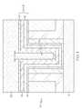
- FIG. 3shows a structure of a replacement high-k metal gate semiconductor device according to an embodiment of the present invention.
- FIGS. 4A-Cshows a process flow diagram which illustrates the progression/method for forming a replacement high-k metal gate semiconductor device according to an embodiment of the present invention.
- FIG. 5show graphs of nitrogen presence during an approach according to an embodiment of the present invention.
- first elementsuch as a first structure (e.g., a first layer) is present on a second element, such as a second structure (e.g. a second layer) wherein intervening elements, such as an interface structure (e.g. interface layer) may be present between the first element and the second element.
- first structuree.g., a first layer
- second structuree.g. a second layer
- intervening elementssuch as an interface structure (e.g. interface layer) may be present between the first element and the second element.
- a structure and method for forming/providing a low gate resistance high-k metal gate transistor deviceis provided that maximizes the volume and eliminates voids in the metal (e.g., Al) fill in the replacement metal gates (RMGs).
- the deviceis formed by providing a set of gate stacks (e.g., replacement metal gate (RMG) stacks) in a trench on a silicon substrate.
- the gate stacks in the trenchmay have various layers such as: a high-k layer (e.g., hafnium dioxide (HfO 2) )) formed over the substrate; a barrier layer (e.g., titanium nitride (TiN), tantalum nitride (TaN), etc.) formed over the high-k layer; a p-type work function (pWF) layer (e.g., titanium nitride (TiN)) formed over the barrier layer; and a n-type work function (nWF) layer (e.g., titanium aluminide (TiAl)) formed over the pWF layer.
- a high-k layere.g., hafnium dioxide (HfO 2)
- a barrier layere.g., titanium nitride (TiN), tantalum nitride (TaN), etc.
- pWFp-type work function
- nWFn-type
- the nWF layerwill be subjected to a nitrogen containing plasma treatment (e.g., nitrogen (N 2 ), ammonia (NH 3 ) gas, etc.) to form a nitridized nWF layer on a top surface of the gate stacks, and an Al containing layer will then be applied over the gas plasma treated layer.
- a nitrogen containing plasma treatmente.g., nitrogen (N 2 ), ammonia (NH 3 ) gas, etc.
- a replacement high-k metal gate semiconductor device 10is shown. As depicted, device 10 includes a set of replacement metal gate (RMG) stacks 24 A-B in a trench 22 formed over a substrate 12 . Various layers such as shown may be utilized to create such features.
- RMGreplacement metal gate
- gate stacks 24 A-B in trench 22may have a high-k dielectric layer (e.g., hafnium dioxide (HfO 2 )) 14 formed over substrate 12 ; a barrier layer (e.g., titanium nitride (TiN), tantalum nitride (TaN)) 16 formed over high-k layer 14 ; a p-type work function (pWF) layer (e.g., titanium nitride (TiN)) 18 formed over barrier layer 16 ; and a n-type work function (nWF) layer (e.g., titanium aluminide (TiAl)) 20 formed over the pWF layer 18 .
- pWFp-type work function
- nWFn-type work function
- trench 22has a gap 26 therein.
- typical processinginvolves applying an Al containing layer 28 over nWF layer 20 so that Al may fill gap 26 and trench 22 with a reflow at high temperature (400° C.-480° C.).
- high temperature400° C.-480° C.
- One problem with this reflow processis the fast diffusion rate of Al at high temperature. Specifically, Al could penetrate through the underneath gate stacks and cause gate leakage and device reliability degradation.
- an additional barrier layere.g., titanium nitride (TiN) 30 is provided.
- This barrier layercan effectively suppress Al diffusion at high reflow temperature.
- application of such a layerhas caused gap 26 of trench 22 to become significantly narrower.
- Such an approachreduced the ability of a subsequent Al 28 to fully fill trench 22 even with high reflow temperature (400° C.-480° C.).
- the void formed in the replacement metal gatewould result in high gate resistance.
- device 100includes a set of replacement metal gate (RMG) stacks 114 A-B in a trench 112 formed over a substrate 102 .
- RMGreplacement metal gate
- Various layerssuch as shown may be utilized to create such features.
- gate stacks 114 A-B in trench 112may have a high-k dielectric layer (e.g., hafnium dioxide (HfO 2 ), hafnium silicate (Hf SiO 4 ), zirconium oxide (ZrO), zirconium silicate (ZrSiO 4 ) or a composite layer of thereof) 104 formed over substrate 102 ; a barrier layer (e.g., titanium nitride (TiN), tantalum nitride (TaN)) 106 formed over high-k layer 104 ; a p-type work function (pWF) layer (e.g., titanium nitride (TiN)) 108 formed over barrier layer 106 ; and a n-type work function (nWF) layer (e.g., titanium aluminide (TiAl)) 110 formed over the pWF layer 108 .
- a high-k dielectric layere.g., hafnium dioxide (
- trench 112has a gap 116 therein.
- a nitrogen containing gas plasma treatmentis applied over nWF layer 110 (e.g. TiAl) to form a top nitridized nWF metal layer 118 (e.g. TiAlN).
- the subsequent stepsinvolve the deposit of an Al containing layer 120 through chemical vapor deposition (CVD) or physical vapor deposition (PVD) approach and Al reflow at high temperature to fill the trench 112 .
- Plasma treatment 122instead of the insertion of additional barrier layer, can maintain the width of gap 116 and allow the full fill of subsequent Al in replacement metal gate trench 112 .
- FIG. 5graphs of element presence (in counts) versus position on device are shown, according to an embodiment of the present invention.
- EELS graph 300 and EDX graph 301 analysisprovides information of element (N, O, Ti, Hf, Ta and Al) intensity versus the position distance from the Si substrate.
- Nitrogen contentis approaching 2.5 ⁇ 10 5 counts at an interface 302 of nWF TiAl and Al (or Al containing alloy). Nitrogen concentration increase is caused by the N containing plasma treatment over nWF metal.
- Both Ti and Al in TiAl alloywas nitridized to form TiAlN at the top surface.
- High nitrogen contentwould retard the Al diffusion in the subsequent Al reflow at high temperature (400° C.-480° C.), which minimizes gate leakage and improves device reliability. Under high reflow temperature, Al can easily fill the replacement high-k metal gate and provides low gate resistance.
- the plasma treatmentcan occur on a nWF metal surface in the presence of an nitrogen containing gas (for example N 2 , NH 3 ) at power range of about 100 W-4000 W, at a temperature range of about 25° C. to about 400° C., at a pressure range of about 0.01-5 Torr.
- an nitrogen containing gasfor example N 2 , NH 3
- the nitridation processis carried out in the presence of N 2 gas, at RF power of 3000 W and pressure of 0.6 Torr, in a single wafer chamber with RPS (remote plasma source).
- design toolscan be provided and configured to create the data sets used to pattern the semiconductor layers as described herein. For example, data sets can be created to generate photomasks used during lithography operations to pattern the layers for structures as described herein.
- Such design toolscan include a collection of one or more modules and can also include hardware, software, or a combination thereof.
- a toolcan be a collection of one or more software modules, hardware modules, software/hardware modules, or any combination or permutation thereof.
- a toolcan be a computing device or other appliance on which software runs or in which hardware is implemented.
- a modulemight be implemented utilizing any form of hardware, software, or a combination thereof.
- processorsfor example, one or more processors, controllers, application-specific integrated circuits (ASIC), programmable logic arrays (PLA)s, logical components, software routines, or other mechanisms might be implemented to make up a module.
- ASICapplication-specific integrated circuits
- PDAprogrammable logic arrays
- logical componentssoftware routines, or other mechanisms might be implemented to make up a module.
- the various modules described hereinmight be implemented as discrete modules or the functions and features described can be shared in part or in total among one or more modules.
- the various features and functionality described hereinmay be implemented in any given application and can be implemented in one or more separate or shared modules in various combinations and permutations.
Landscapes
- Engineering & Computer Science (AREA)
- Chemical & Material Sciences (AREA)
- Composite Materials (AREA)
- Physics & Mathematics (AREA)
- Condensed Matter Physics & Semiconductors (AREA)
- General Physics & Mathematics (AREA)
- Manufacturing & Machinery (AREA)
- Computer Hardware Design (AREA)
- Microelectronics & Electronic Packaging (AREA)
- Power Engineering (AREA)
- Electrodes Of Semiconductors (AREA)
Abstract
Description
Claims (10)
Priority Applications (1)
| Application Number | Priority Date | Filing Date | Title |
|---|---|---|---|
| US13/654,987US8772100B2 (en) | 2012-10-18 | 2012-10-18 | Structure and method for forming a low gate resistance high-K metal gate transistor device |
Applications Claiming Priority (1)
| Application Number | Priority Date | Filing Date | Title |
|---|---|---|---|
| US13/654,987US8772100B2 (en) | 2012-10-18 | 2012-10-18 | Structure and method for forming a low gate resistance high-K metal gate transistor device |
Publications (2)
| Publication Number | Publication Date |
|---|---|
| US20140110790A1 US20140110790A1 (en) | 2014-04-24 |
| US8772100B2true US8772100B2 (en) | 2014-07-08 |
Family
ID=50484588
Family Applications (1)
| Application Number | Title | Priority Date | Filing Date |
|---|---|---|---|
| US13/654,987Active2032-11-27US8772100B2 (en) | 2012-10-18 | 2012-10-18 | Structure and method for forming a low gate resistance high-K metal gate transistor device |
Country Status (1)
| Country | Link |
|---|---|
| US (1) | US8772100B2 (en) |
Cited By (2)
| Publication number | Priority date | Publication date | Assignee | Title |
|---|---|---|---|---|
| US20150076623A1 (en)* | 2013-09-13 | 2015-03-19 | United Microelectronics Corp. | Metal gate transistor and method for fabricating the same |
| US10529823B2 (en) | 2018-05-29 | 2020-01-07 | International Business Machines Corporation | Method of manufacturing a semiconductor device having a metal gate with different lateral widths between spacers |
Families Citing this family (9)
| Publication number | Priority date | Publication date | Assignee | Title |
|---|---|---|---|---|
| US20140120711A1 (en)* | 2012-10-26 | 2014-05-01 | United Microelectronics Corp. | Method of forming metal gate |
| CN104347411B (en)* | 2013-08-01 | 2018-04-13 | 中国科学院微电子研究所 | Method for Adjusting Equivalent Work Function of Metal Gate Electrode |
| KR20160021564A (en)* | 2014-08-18 | 2016-02-26 | 삼성전자주식회사 | Semiconductor device and method for the same |
| CN105514105B (en)* | 2014-09-26 | 2019-08-06 | 联华电子股份有限公司 | Integrated circuit and forming method thereof |
| CN105552116B (en)* | 2014-10-30 | 2021-05-11 | 联华电子股份有限公司 | Metal gate structure and method of forming the same |
| US9502301B2 (en) | 2014-12-29 | 2016-11-22 | Globalfoundries Inc. | Fabrication methods for multi-layer semiconductor structures |
| US9698241B1 (en) | 2016-03-16 | 2017-07-04 | GlobalFoundries, Inc. | Integrated circuits with replacement metal gates and methods for fabricating the same |
| KR102399497B1 (en) | 2017-05-29 | 2022-05-19 | 에스케이하이닉스 주식회사 | Semiconductor device having buried gate structure and method for manufacturing the same |
| JP7387685B2 (en)* | 2021-09-17 | 2023-11-28 | 株式会社Kokusai Electric | Semiconductor device manufacturing method, substrate processing method, program, and substrate processing device |
Citations (12)
| Publication number | Priority date | Publication date | Assignee | Title |
|---|---|---|---|---|
| US5244535A (en) | 1991-03-15 | 1993-09-14 | Texas Instruments Incorporated | Method of manufacturing a semiconductor device including plasma treatment of contact holes |
| US6074941A (en) | 1998-04-20 | 2000-06-13 | United Semiconductor Corp. | Method of forming a via with plasma treatment of SOG |
| US6232217B1 (en) | 2000-06-05 | 2001-05-15 | Chartered Semiconductor Manufacturing Ltd. | Post treatment of via opening by N-containing plasma or H-containing plasma for elimination of fluorine species in the FSG near the surfaces of the via opening |
| US6431182B1 (en) | 1999-10-27 | 2002-08-13 | Advanced Micro Devices, Inc. | Plasma treatment for polymer removal after via etch |
| US20060205192A1 (en) | 2005-03-09 | 2006-09-14 | Varian Semiconductor Equipment Associates, Inc. | Shallow-junction fabrication in semiconductor devices via plasma implantation and deposition |
| US20060249755A1 (en) | 2005-05-06 | 2006-11-09 | Hsiu-Lan Kuo | Method to prevent arcing during deep via plasma etching |
| US7217652B1 (en) | 2000-09-21 | 2007-05-15 | Spansion Llc | Method of forming highly conductive semiconductor structures via plasma etch |
| US7531896B1 (en) | 2004-04-09 | 2009-05-12 | National Semiconductor Corporation | Semiconductor device having a minimal via resistance created by applying a nitrogen plasma to a titanium via liner |
| US7759796B2 (en) | 2007-05-24 | 2010-07-20 | Kabushiki Kaisha Toshiba | Semiconductor device with two barrier layers formed between copper-containing line layer and aluminum-containing conductive layer |
| US7786005B2 (en) | 2005-03-25 | 2010-08-31 | Nec Electronics Corporation | Method for manufacturing semiconductor device to form a via hole |
| US8207595B2 (en) | 2010-10-05 | 2012-06-26 | Taiwan Semiconductor Manufacturing Company, Ltd. | Semiconductor having a high aspect ratio via |
| US8564072B2 (en)* | 2010-04-02 | 2013-10-22 | Taiwan Semiconductor Manufacturing Company, Ltd. | Semiconductor device having a blocking structure and method of manufacturing the same |
- 2012
- 2012-10-18USUS13/654,987patent/US8772100B2/enactiveActive
Patent Citations (12)
| Publication number | Priority date | Publication date | Assignee | Title |
|---|---|---|---|---|
| US5244535A (en) | 1991-03-15 | 1993-09-14 | Texas Instruments Incorporated | Method of manufacturing a semiconductor device including plasma treatment of contact holes |
| US6074941A (en) | 1998-04-20 | 2000-06-13 | United Semiconductor Corp. | Method of forming a via with plasma treatment of SOG |
| US6431182B1 (en) | 1999-10-27 | 2002-08-13 | Advanced Micro Devices, Inc. | Plasma treatment for polymer removal after via etch |
| US6232217B1 (en) | 2000-06-05 | 2001-05-15 | Chartered Semiconductor Manufacturing Ltd. | Post treatment of via opening by N-containing plasma or H-containing plasma for elimination of fluorine species in the FSG near the surfaces of the via opening |
| US7217652B1 (en) | 2000-09-21 | 2007-05-15 | Spansion Llc | Method of forming highly conductive semiconductor structures via plasma etch |
| US7531896B1 (en) | 2004-04-09 | 2009-05-12 | National Semiconductor Corporation | Semiconductor device having a minimal via resistance created by applying a nitrogen plasma to a titanium via liner |
| US20060205192A1 (en) | 2005-03-09 | 2006-09-14 | Varian Semiconductor Equipment Associates, Inc. | Shallow-junction fabrication in semiconductor devices via plasma implantation and deposition |
| US7786005B2 (en) | 2005-03-25 | 2010-08-31 | Nec Electronics Corporation | Method for manufacturing semiconductor device to form a via hole |
| US20060249755A1 (en) | 2005-05-06 | 2006-11-09 | Hsiu-Lan Kuo | Method to prevent arcing during deep via plasma etching |
| US7759796B2 (en) | 2007-05-24 | 2010-07-20 | Kabushiki Kaisha Toshiba | Semiconductor device with two barrier layers formed between copper-containing line layer and aluminum-containing conductive layer |
| US8564072B2 (en)* | 2010-04-02 | 2013-10-22 | Taiwan Semiconductor Manufacturing Company, Ltd. | Semiconductor device having a blocking structure and method of manufacturing the same |
| US8207595B2 (en) | 2010-10-05 | 2012-06-26 | Taiwan Semiconductor Manufacturing Company, Ltd. | Semiconductor having a high aspect ratio via |
Cited By (5)
| Publication number | Priority date | Publication date | Assignee | Title |
|---|---|---|---|---|
| US20150076623A1 (en)* | 2013-09-13 | 2015-03-19 | United Microelectronics Corp. | Metal gate transistor and method for fabricating the same |
| US9196546B2 (en)* | 2013-09-13 | 2015-11-24 | United Microelectronics Corp. | Metal gate transistor |
| US9825144B2 (en) | 2013-09-13 | 2017-11-21 | United Microelectronics Corp. | Semiconductor device having metal gate structure |
| US10529823B2 (en) | 2018-05-29 | 2020-01-07 | International Business Machines Corporation | Method of manufacturing a semiconductor device having a metal gate with different lateral widths between spacers |
| US10734501B2 (en) | 2018-05-29 | 2020-08-04 | International Business Machines Corporation | Metal gate structure having gate metal layer with a top portion width smaller than a bottom portion width to reduce transistor gate resistance |
Also Published As
| Publication number | Publication date |
|---|---|
| US20140110790A1 (en) | 2014-04-24 |
Similar Documents
| Publication | Publication Date | Title |
|---|---|---|
| US8772100B2 (en) | Structure and method for forming a low gate resistance high-K metal gate transistor device | |
| US9685441B2 (en) | Semiconductor device with tunable work function | |
| US10340192B2 (en) | FinFET gate structure and method for fabricating the same | |
| US10276697B1 (en) | Negative capacitance FET with improved reliability performance | |
| US10832974B2 (en) | FinFET gate structure and method for fabricating the same | |
| US9257349B2 (en) | Method of scavenging impurities in forming a gate stack having an interfacial layer | |
| US9054130B2 (en) | Bottle-neck recess in a semiconductor device | |
| CN104241291B (en) | In-line memory and forming method thereof | |
| US8952462B2 (en) | Method and apparatus of forming a gate | |
| US20110256682A1 (en) | Multiple Deposition, Multiple Treatment Dielectric Layer For A Semiconductor Device | |
| CN103854982B (en) | Method for manufacturing semiconductor device | |
| CN106409677B (en) | Semiconductor device and method of forming the same | |
| US10008494B2 (en) | Semiconductor component and method for fabricating the same | |
| US8853069B2 (en) | Field effect transistor and method of fabrication | |
| US10276447B2 (en) | Semiconductor structures and methods of forming the same | |
| CN101740372A (en) | Gate structure including modified high-k gate dielectric and metal gate interface | |
| CN104979391A (en) | Semiconductor element and manufacturing method thereof | |
| CN103730418A (en) | Method for manufacturing semiconductor device | |
| US8658490B2 (en) | Passivating point defects in high-K gate dielectric layers during gate stack formation | |
| CN106328529B (en) | MOS transistor and forming method thereof | |
| US9269626B2 (en) | Integrated circuit structure and method for manufacturing thereof | |
| CN106571299A (en) | PMOS transistor and formation method thereof |
Legal Events
| Date | Code | Title | Description |
|---|---|---|---|
| AS | Assignment | Owner name:GLOBALFOUNDRIES INC., CAYMAN ISLANDS Free format text:ASSIGNMENT OF ASSIGNORS INTEREST;ASSIGNORS:HUANG, JINGYAN;WONG, KEITH KWONG HON;REEL/FRAME:029269/0687 Effective date:20121016 Owner name:INTERNATIONAL BUSINESS MACHINES CORPORATION, NEW Y Free format text:ASSIGNMENT OF ASSIGNORS INTEREST;ASSIGNORS:HUANG, JINGYAN;WONG, KEITH KWONG HON;REEL/FRAME:029269/0687 Effective date:20121016 | |
| STCF | Information on status: patent grant | Free format text:PATENTED CASE | |
| CC | Certificate of correction | ||
| AS | Assignment | Owner name:GLOBALFOUNDRIES U.S. 2 LLC, NEW YORK Free format text:ASSIGNMENT OF ASSIGNORS INTEREST;ASSIGNOR:INTERNATIONAL BUSINESS MACHINES CORPORATION;REEL/FRAME:036550/0001 Effective date:20150629 | |
| AS | Assignment | Owner name:GLOBALFOUNDRIES INC., CAYMAN ISLANDS Free format text:ASSIGNMENT OF ASSIGNORS INTEREST;ASSIGNORS:GLOBALFOUNDRIES U.S. 2 LLC;GLOBALFOUNDRIES U.S. INC.;REEL/FRAME:036779/0001 Effective date:20150910 | |
| MAFP | Maintenance fee payment | Free format text:PAYMENT OF MAINTENANCE FEE, 4TH YEAR, LARGE ENTITY (ORIGINAL EVENT CODE: M1551) Year of fee payment:4 | |
| AS | Assignment | Owner name:WILMINGTON TRUST, NATIONAL ASSOCIATION, DELAWARE Free format text:SECURITY AGREEMENT;ASSIGNOR:GLOBALFOUNDRIES INC.;REEL/FRAME:049490/0001 Effective date:20181127 | |
| AS | Assignment | Owner name:GLOBALFOUNDRIES U.S. INC., CALIFORNIA Free format text:ASSIGNMENT OF ASSIGNORS INTEREST;ASSIGNOR:GLOBALFOUNDRIES INC.;REEL/FRAME:054633/0001 Effective date:20201022 | |
| AS | Assignment | Owner name:GLOBALFOUNDRIES INC., CAYMAN ISLANDS Free format text:RELEASE BY SECURED PARTY;ASSIGNOR:WILMINGTON TRUST, NATIONAL ASSOCIATION;REEL/FRAME:054636/0001 Effective date:20201117 | |
| AS | Assignment | Owner name:GLOBALFOUNDRIES U.S. INC., NEW YORK Free format text:RELEASE BY SECURED PARTY;ASSIGNOR:WILMINGTON TRUST, NATIONAL ASSOCIATION;REEL/FRAME:056987/0001 Effective date:20201117 | |
| MAFP | Maintenance fee payment | Free format text:PAYMENT OF MAINTENANCE FEE, 8TH YEAR, LARGE ENTITY (ORIGINAL EVENT CODE: M1552); ENTITY STATUS OF PATENT OWNER: LARGE ENTITY Year of fee payment:8 |