US8771577B2 - Light emitting device with molded wavelength converting layer - Google Patents
Light emitting device with molded wavelength converting layerDownload PDFInfo
- Publication number
- US8771577B2 US8771577B2US12/706,149US70614910AUS8771577B2US 8771577 B2US8771577 B2US 8771577B2US 70614910 AUS70614910 AUS 70614910AUS 8771577 B2US8771577 B2US 8771577B2
- Authority
- US
- United States
- Prior art keywords
- light source
- mold
- flexible film
- wavelength converting
- film
- Prior art date
- Legal status (The legal status is an assumption and is not a legal conclusion. Google has not performed a legal analysis and makes no representation as to the accuracy of the status listed.)
- Active, expires
Links
Images


Classifications
- H—ELECTRICITY
- H10—SEMICONDUCTOR DEVICES; ELECTRIC SOLID-STATE DEVICES NOT OTHERWISE PROVIDED FOR
- H10H—INORGANIC LIGHT-EMITTING SEMICONDUCTOR DEVICES HAVING POTENTIAL BARRIERS
- H10H20/00—Individual inorganic light-emitting semiconductor devices having potential barriers, e.g. light-emitting diodes [LED]
- H10H20/80—Constructional details
- H10H20/85—Packages
- H10H20/851—Wavelength conversion means
- B—PERFORMING OPERATIONS; TRANSPORTING
- B29—WORKING OF PLASTICS; WORKING OF SUBSTANCES IN A PLASTIC STATE IN GENERAL
- B29C—SHAPING OR JOINING OF PLASTICS; SHAPING OF MATERIAL IN A PLASTIC STATE, NOT OTHERWISE PROVIDED FOR; AFTER-TREATMENT OF THE SHAPED PRODUCTS, e.g. REPAIRING
- B29C43/00—Compression moulding, i.e. applying external pressure to flow the moulding material; Apparatus therefor
- B29C43/02—Compression moulding, i.e. applying external pressure to flow the moulding material; Apparatus therefor of articles of definite length, i.e. discrete articles
- B29C43/18—Compression moulding, i.e. applying external pressure to flow the moulding material; Apparatus therefor of articles of definite length, i.e. discrete articles incorporating preformed parts or layers, e.g. compression moulding around inserts or for coating articles
- H—ELECTRICITY
- H10—SEMICONDUCTOR DEVICES; ELECTRIC SOLID-STATE DEVICES NOT OTHERWISE PROVIDED FOR
- H10H—INORGANIC LIGHT-EMITTING SEMICONDUCTOR DEVICES HAVING POTENTIAL BARRIERS
- H10H20/00—Individual inorganic light-emitting semiconductor devices having potential barriers, e.g. light-emitting diodes [LED]
- H10H20/01—Manufacture or treatment
- H10H20/011—Manufacture or treatment of bodies, e.g. forming semiconductor layers
- H10H20/013—Manufacture or treatment of bodies, e.g. forming semiconductor layers having light-emitting regions comprising only Group III-V materials
- H10H20/0137—Manufacture or treatment of bodies, e.g. forming semiconductor layers having light-emitting regions comprising only Group III-V materials the light-emitting regions comprising nitride materials
- H—ELECTRICITY
- H10—SEMICONDUCTOR DEVICES; ELECTRIC SOLID-STATE DEVICES NOT OTHERWISE PROVIDED FOR
- H10H—INORGANIC LIGHT-EMITTING SEMICONDUCTOR DEVICES HAVING POTENTIAL BARRIERS
- H10H20/00—Individual inorganic light-emitting semiconductor devices having potential barriers, e.g. light-emitting diodes [LED]
- H10H20/01—Manufacture or treatment
- H10H20/011—Manufacture or treatment of bodies, e.g. forming semiconductor layers
- H10H20/018—Bonding of wafers
- H—ELECTRICITY
- H10—SEMICONDUCTOR DEVICES; ELECTRIC SOLID-STATE DEVICES NOT OTHERWISE PROVIDED FOR
- H10H—INORGANIC LIGHT-EMITTING SEMICONDUCTOR DEVICES HAVING POTENTIAL BARRIERS
- H10H20/00—Individual inorganic light-emitting semiconductor devices having potential barriers, e.g. light-emitting diodes [LED]
- H10H20/80—Constructional details
- H10H20/85—Packages
- H10H20/851—Wavelength conversion means
- H10H20/8511—Wavelength conversion means characterised by their material, e.g. binder
- H10H20/8512—Wavelength conversion materials
- H10H20/8513—Wavelength conversion materials having two or more wavelength conversion materials
- H—ELECTRICITY
- H10—SEMICONDUCTOR DEVICES; ELECTRIC SOLID-STATE DEVICES NOT OTHERWISE PROVIDED FOR
- H10H—INORGANIC LIGHT-EMITTING SEMICONDUCTOR DEVICES HAVING POTENTIAL BARRIERS
- H10H20/00—Individual inorganic light-emitting semiconductor devices having potential barriers, e.g. light-emitting diodes [LED]
- H10H20/80—Constructional details
- H10H20/85—Packages
- H10H20/852—Encapsulations
- H10H20/854—Encapsulations characterised by their material, e.g. epoxy or silicone resins
- H—ELECTRICITY
- H10—SEMICONDUCTOR DEVICES; ELECTRIC SOLID-STATE DEVICES NOT OTHERWISE PROVIDED FOR
- H10H—INORGANIC LIGHT-EMITTING SEMICONDUCTOR DEVICES HAVING POTENTIAL BARRIERS
- H10H20/00—Individual inorganic light-emitting semiconductor devices having potential barriers, e.g. light-emitting diodes [LED]
- H10H20/80—Constructional details
- H10H20/85—Packages
- H10H20/855—Optical field-shaping means, e.g. lenses
- H—ELECTRICITY
- H01—ELECTRIC ELEMENTS
- H01L—SEMICONDUCTOR DEVICES NOT COVERED BY CLASS H10
- H01L25/00—Assemblies consisting of a plurality of semiconductor or other solid state devices
- H01L25/03—Assemblies consisting of a plurality of semiconductor or other solid state devices all the devices being of a type provided for in a single subclass of subclasses H10B, H10D, H10F, H10H, H10K or H10N, e.g. assemblies of rectifier diodes
- H01L25/04—Assemblies consisting of a plurality of semiconductor or other solid state devices all the devices being of a type provided for in a single subclass of subclasses H10B, H10D, H10F, H10H, H10K or H10N, e.g. assemblies of rectifier diodes the devices not having separate containers
- H01L25/075—Assemblies consisting of a plurality of semiconductor or other solid state devices all the devices being of a type provided for in a single subclass of subclasses H10B, H10D, H10F, H10H, H10K or H10N, e.g. assemblies of rectifier diodes the devices not having separate containers the devices being of a type provided for in group H10H20/00
- H01L25/0753—Assemblies consisting of a plurality of semiconductor or other solid state devices all the devices being of a type provided for in a single subclass of subclasses H10B, H10D, H10F, H10H, H10K or H10N, e.g. assemblies of rectifier diodes the devices not having separate containers the devices being of a type provided for in group H10H20/00 the devices being arranged next to each other
- H—ELECTRICITY
- H01—ELECTRIC ELEMENTS
- H01L—SEMICONDUCTOR DEVICES NOT COVERED BY CLASS H10
- H01L2924/00—Indexing scheme for arrangements or methods for connecting or disconnecting semiconductor or solid-state bodies as covered by H01L24/00
- H01L2924/0001—Technical content checked by a classifier
- H01L2924/0002—Not covered by any one of groups H01L24/00, H01L24/00 and H01L2224/00
Definitions
- the present inventionrelates to a wavelength converted light emitting device.
- LEDslight emitting diodes
- RCLEDsresonant cavity light emitting diodes
- VCSELsvertical cavity laser diodes
- edge emitting lasersare among the most efficient light sources currently available.
- Materials systems currently of interest in the manufacture of high-brightness light emitting devices capable of operation across the visible spectruminclude Group III-V semiconductors, particularly binary, ternary, and quaternary alloys of gallium, aluminum, indium, and nitrogen, also referred to as III-nitride materials.
- III-nitride light emitting devicesare fabricated by epitaxially growing a stack of semiconductor layers of different compositions and dopant concentrations on a sapphire, silicon carbide, III-nitride, or other suitable substrate by metal-organic chemical vapor deposition (MOCVD), molecular beam epitaxy (MBE), or other epitaxial techniques.
- MOCVDmetal-organic chemical vapor deposition
- MBEmolecular beam epitaxy
- the stackoften includes one or more n-type layers doped with, for example, Si, formed over the substrate, one or more light emitting layers in an active region formed over the n-type layer or layers, and one or more p-type layers doped with, for example, Mg, formed over the active region. Electrical contacts are formed on the n- and p-type regions.
- FIG. 1illustrates an LED described in more detail in U.S. Pat. No. 7,352,011, which is incorporated herein by reference.
- An LED 10is mounted on a support structure (not shown in FIG. 1 ).
- An inner lens 64is molded over LED 10 .
- Lens 64is formed as follows: a mold in the shape of lens 64 is positioned over LED 10 .
- the moldmay be lined with a non-stick film.
- the moldis filled with a suitable transparent heat-curable liquid lens material such as silicone or epoxy.
- a vacuum sealis created between the periphery of the support structure and the mold, and the two pieces are pressed against each other so that each LED die 10 is inserted into the liquid lens material and the lens material is under compression.
- the moldis then heated to about 150 degrees centigrade (or other suitable temperature) for a time to harden the lens material.
- the support structureis then separated from the mold.
- an outer phosphor/silicone shell 66 of any thicknessis formed directly over the inner lens 64 .
- An outer lens 68may be formed over the phosphor/silicone shell 66 using another mold to further shape the beam.
- the thickness of the wavelength converting materialmay be tightly controlled.
- a flexible filmcomprising a wavelength converting material is positioned over a light source.
- the flexible filmis conformed to a predetermined shape.
- the light sourceis a light emitting diode mounted on a support substrate.
- the diodeis aligned with an indentation in a mold such that the flexible film is disposed between the support substrate and the mold.
- Transparent molding materialis disposed between the support substrate and the mold. The support substrate and the mold are pressed together to cause the molding material to fill the indentation.
- the flexible filmconforms to the shape of the light source or the mold.
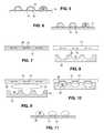
- FIG. 1illustrates a prior art LED mounted on a support structure and covered with a molded lens.
- FIG. 2illustrates a flexible wavelength converting film disposed between a mold and multiple LEDs mounted on a support substrate.
- FIG. 3illustrates molding material disposed between LEDs mounted on a support substrate and a wavelength converting film lining a mold.
- FIG. 4illustrates the molding material of FIG. 3 molded into lenses over the LEDs.
- FIG. 5illustrates the structure of FIG. 4 after removing the mold.
- FIG. 6illustrates the structure of FIG. 5 after removing a support film.
- FIG. 7illustrates a flexible wavelength converting film positioned over LEDs mounted on a support substrate.
- FIG. 8illustrates the structure of FIG. 7 flipped over and positioned over a mold.
- FIG. 9illustrates molding material disposed between a wavelength converting film and a mold.
- FIG. 10illustrates the molding material of FIG. 9 molded into lenses over the LEDs.
- FIG. 11illustrates the structure of FIG. 10 after removing the mold.
- FIG. 12illustrates a first wavelength converting film positioned under LEDs mounted on a support substrate and a second wavelength converting film positioned over a mold.
- FIG. 13illustrates molding material disposed between the two wavelength converting films illustrated in FIG. 13 .
- FIG. 14illustrates the molding material of FIG. 13 formed into lenses over the LEDs.
- FIG. 15illustrates the structure of FIG. 14 after removing the mold.
- FIG. 16illustrates the structure of FIG. 15 after removing a support film.
- the thickness of phosphor layer 66determines the characteristics such as the color temperature of the light emitted by the device.
- the thickness of phosphor layer 66can vary based on variations in the alignment of the phosphor mold, which may undesirably alter the characteristics of the emitted light.
- phosphor layer 66may be in the range of 100 ⁇ m thick.
- the mold-alignment tolerance of the phosphor moldmay be in the range of 30-50 ⁇ m.
- the high mold-alignment tolerance relative to the target thickness of the phosphorcan cause variations in the thickness of the phosphor that undesirably shift the color point of light emitted from the device.
- a wavelength converting materialis formed into a flexible film which is molded over a light source such as a semiconductor light emitting device.
- the filmmay be fully or partially cured transparent material, such as silicone, which is filled with phosphor.
- the wavelength converting filmmay be formed separate from the molding process, which permits tight control of the thickness of the wavelength converting film as well as testing and verification of the characteristics of the film prior to molding. Molding and other processing steps according to the invention may be performed as described in U.S. Pat. No. 7,352,011.
- the wavelength converting flexible filmis formed on a support film such as an ethylene tetrafluoroethylene film, for example by spreading a mixture of phosphor and silicone over the support film then fully or partially curing the silicone in the wavelength converting film.
- the wavelength converting materialmay be temporarily protected by another ethylene tetrafluorethylene film, which is removed before the processing described below. After processing, the support film is generally peeled away from the wavelength converting film.
- the support filmsserves as a release film, which releases a molded lens from the mold.
- a heat dissipating material such as diamondmay be added to the wavelength converting film.
- a material such as diamondmay be added to the wavelength converting film to adjust the refractive index of the film, to improve optical transmission, and/or to improve conversion.
- a light sourceis provided.
- the light sourceis an LED
- any suitable light sourcemay be used.
- the light sourceis a III-nitride LED that emits blue or UV light
- semiconductor light emitting devices besides LEDs and semiconductor light emitting devices made from other materials systemssuch as other III-V materials, III-phosphide, III-arsenide, II-VI materials, or Si-based materials may be used.
- a conventional III-nitride LED 10is formed by first growing a semiconductor structure on a growth substrate.
- An n-type regionis typically grown first and may include multiple layers of different compositions and dopant concentration including, for example, preparation layers such as buffer layers or nucleation layers, which may be n-type or not intentionally doped, release layers designed to facilitate later release of the substrate or thinning of the semiconductor structure after substrate removal, and n- or even p-type device layers designed for particular optical or electrical properties desirable for the light emitting region to efficiently emit light.
- a light emitting or active regionis grown over the n-type region.
- suitable light emitting regionsinclude a single thick or thin light emitting layer, or a multiple quantum well light emitting region including multiple thin or thick quantum well light emitting layers separated by barrier layers.
- a p-type regionis grown over the light emitting region. Like the n-type region, the p-type region may include multiple layers of different composition, thickness, and dopant concentration, including layers that are not intentionally doped, or n-type layers.
- n-layersPortions of the p-layers and active layer are etched away to expose an n-layer for metallization. In this way the p-contact and n-contact are on the same side of the chip and can be directly electrically attached to contact pads on a suitable mount.
- the devicecan be mounted such that light is extracted from the top surface (i.e. the surface on which the electrical contacts are formed) or the bottom surface (i.e. a flip chip with reflective contacts).
- the growth substratemay be removed from the semiconductor structure or may remain a part of the completed device.
- the semiconductor structuremay be thinned, and the surface of the n-type region exposed by removing the substrate may be textured to improve light extraction, for example by roughening or forming a photonic crystal structure.
- an n-contactis formed on one side of the semiconductor structure, and a p-contact is formed on the other side of the semiconductor structure. Electrical contact to one of the p- or n-contacts is typically made with a wire or a metal bridge, and the other contact is directly bonded to a contact pad on the mount.
- the examples belowinclude a flip chip device from which the growth substrate has been removed, any suitable device structure may be used.
- One or more wavelength converting materialssuch as phosphors or dyes may be included in the flexible film molded over the LED.
- Non-wavelength-converting materialssuch as TiO x particles may be included in the flexible film, for example to cause light scattering or to improve the off-state white appearance of the device.
- the flexible filmmay be textured to change the optical properties, for example by embossing microlenses to improve light extraction.
- An LED combined with one or more wavelength converting materialsmay be used to create white light or monochromatic light of other colors. All or only a portion of the light emitted by the LED may be converted by the wavelength converting material. Though in the examples below the wavelength converting materials are powder phosphors, any suitable wavelength converting material may be used. Unconverted light may be part of the final spectrum of light, though it need not be.
- Examples of common combinationsinclude a blue-emitting LED combined with a yellow-emitting phosphor, a blue-emitting LED combined with green- and red-emitting phosphors, a UV-emitting LED combined with blue- and yellow-emitting phosphors, and a UV-emitting LED combined with blue-, green-, and red-emitting phosphors.
- Wavelength converting materials emitting other colors of lightmay be added to tailor the spectrum of light emitted from the device. Multiple wavelength converting materials may be mixed and formed in a single film, formed as discrete layers in a single film, or formed as mixed or discrete layers in multiple films.
- Wavelength converting materials formed in a flexible filmmay be combined in a device with other conventional wavelength converting materials, such as pre-formed ceramic phosphor layers that are glued or bonded to the LED, or a powder phosphor disposed in an organic encapsulant that is stenciled, screen printed, sprayed, sedimented, evaporated, sputtered, or otherwise dispensed over the LED.
- other conventional wavelength converting materialssuch as pre-formed ceramic phosphor layers that are glued or bonded to the LED, or a powder phosphor disposed in an organic encapsulant that is stenciled, screen printed, sprayed, sedimented, evaporated, sputtered, or otherwise dispensed over the LED.
- FIGS. 2-6illustrate forming a first embodiment of the invention.
- FIG. 2several LEDs 10 mounted on a support substrate 12 are aligned with indentations 22 corresponding to each LED 10 in a mold 20 .
- a wavelength converting flexible film 14is disposed on a support film 16 .
- the wavelength converting film 14 and support film 16are disposed between support substrate 12 and mold 20 .
- the wavelength converting filmis fully cured.
- support film 16is a material which prevents the molding material 24 described in FIG. 3 from adhering to mold 20 , such as ethylene tetrafluoroethylene.
- the thickness of wavelength converting film 14depends on the wavelength converting material used and the desired characteristics of the light emitted from the device.
- the thickness of wavelength converting film 14may be between 10 and 200 ⁇ m in some embodiments, between 40 and 60 ⁇ m in some embodiments, and 50 ⁇ m in some embodiments.
- support film 16 and wavelength converting film 14are pressed against mold 20 such that they line the indentations 22 in mold 20 .
- support film 16 and wavelength converting film 14may be stretched over the mold indentations, then a reduced pressure environment or vacuum may be created which pulls the films into the mold indentations as illustrated in FIG. 3 .
- Molding material 24is disposed between mold 20 and support substrate 12 .
- indentations 22may take any suitable shape, typically indentations 22 are shaped as lenses and molding material 24 is transparent.
- molding material 24is often silicone, any suitable molding material may be used.
- mold 20 and support substrate 12are pressed together to force molding material 24 to fill indentations 22 in mold 20 and to adhere to LEDs 10 and support substrate 12 .
- a vacuum or reduced pressure environmentmay be applied to draw molding material 24 into indentations 22 .
- Lenses 26are formed on each LED 10 .
- Molding material 24may be cured as appropriate to the molding material, for example by heating, to form solid lenses 26 .
- mold 20is removed, leaving lenses 26 formed of molding material 24 over each LED 10 .
- Wavelength converting film 14 and support film 16are disposed over each lens 26 and between adjacent lenses.
- wavelength converting film 14is spaced apart from LED 10 by lens 26 .
- FIGS. 7-11illustrate forming a device with the wavelength converting film in direct contact with the LED.
- Wavelength converting film 28is positioned over LEDs 10 , which are attached to support substrate 12 .
- Wavelength converting film 28may have the same characteristics as the wavelength converting film 14 described above, and may be formed on a support film. In some embodiments, wavelength converting film 28 is only partially cured.
- LEDs 10are aligned with indentations 22 corresponding to each LED 10 in a mold 20 .
- molding material 24is disposed between mold 20 and wavelength converting film 28 .
- Mold 20may be lined with an optional release film, not shown in FIG. 9 .
- mold 20 and support substrate 12are pressed together to force molding material 24 to take the shape of indentations 22 in mold 20 to form lenses 26 over each LED 10 .
- Molding material 24forces wavelength converting film 28 to conform to the shape of LEDs 10 and support substrate 12 and to adhere to LEDs 10 and support substrate 12 .
- Molding material 24adheres to wavelength converting film 28 .
- Molding material 24may be cured as described above.
- wavelength converting film 28is in direct contact with LEDs 10 and support substrate 12 between LEDs 10 . Lenses 26 are disposed over wavelength converting film 28 .
- FIGS. 12-16illustrate forming a device with two wavelength converting films.
- a flexible wavelength converting film 28is positioned over LEDs 10 and support substrate 12 , as described above in reference to FIG. 7 .
- Wavelength converting film 28may be formed on a support film and in some embodiments is partially cured.
- a wavelength converting film 14 and a support film 16 as described above in reference to FIG. 2are positioned over a mold 20 .
- wavelength converting film 14is fully cured.
- Indentations 22 in mold 20are aligned with LEDs 10 .
- wavelength converting film 14 and support film 16are pressed into the indentations 22 in mold 20 such that they line mold 20 , as described above in reference to FIG. 3 .
- Molding material 24is dispensed between wavelength converting film 28 and wavelength converting film 14 .
- mold 20 and support structure 12are pressed together. Molding material 24 fills the indentations 22 in mold 20 to form lenses over LEDs 10 . Molding material 24 forces wavelength converting film 28 to conform to the shape of LEDs 10 and support substrate 12 .
- FIG. 16support film 16 is removed.
- a first wavelength converting film 28directly contacts the top surface of LEDs 10 .
- Lenses 26are disposed over first wavelength converting film 28 .
- a second wavelength converting film 14is disposed over lenses 26 .
- the first and second wavelength converting filmsmay include different wavelength converting materials.
- LEDs 10may emit blue light
- one of the wavelength converting filmsmay include a yellow- or green-emitting phosphor
- the other of the wavelength converting filmsmay include a red-emitting phosphor.
- an optional, additional transparent layermay be molded over the devices illustrated in FIGS. 6 and 16 to protect wavelength converting film 14 .
- the additional transparent layermay be shaped to increase extraction efficiency and/or sized to provide a desired source size.
- the materialmay be selected to improve color vs. angle of the light emitted from the device or to increase overall light output. All or part of the surface of the additional transparent layer may be textured to improve light extraction.
- lens 26has smaller index of refraction than the additional transparent layer, which may reduce the number of unconverted blue photons scattered back toward the LED where they can be lost to absorption.
- the index of refraction of lens 26is 1.4 or lower and the index of refraction of the additional transparent layer is 1.5 or higher.
- a molded wavelength converting film as described in the embodiments abovemay have several advantages over conventional wavelength converting layers.
- the flexible wavelength converting filmsmay be formed separate from the molding process. Color measurements can be performed in advance to achieve a desired color and films may be tailored to a given LED emission color. Wavelength converting films may be manufactured in large areas at low cost.
- the distance between LED 10 and wavelength converting film 14 , the thickness of the wavelength converting films, and the uniformity of the thickness of the wavelength converting films over the LEDmay be tightly controlled and optimized to improve extraction efficiency, color control, and source size.
- a near-remote wavelength converting filmmay be exposed to less heat from the LED, which may allow the use of wavelength converting materials that are temperature sensitive.
- the photon density in a near-remote wavelength converting layermay be decreased, which may increase light output from the device.
- the absorption cross section of the LEDmay be reduced with a near-remote wavelength converting film, which may increase extraction efficiency.
Landscapes
- Engineering & Computer Science (AREA)
- Power Engineering (AREA)
- Microelectronics & Electronic Packaging (AREA)
- Mechanical Engineering (AREA)
- Physics & Mathematics (AREA)
- Condensed Matter Physics & Semiconductors (AREA)
- General Physics & Mathematics (AREA)
- Computer Hardware Design (AREA)
- Led Device Packages (AREA)
Abstract
Description
Claims (19)
Priority Applications (9)
| Application Number | Priority Date | Filing Date | Title |
|---|---|---|---|
| US12/706,149US8771577B2 (en) | 2010-02-16 | 2010-02-16 | Light emitting device with molded wavelength converting layer |
| TW104143940ATWI612693B (en) | 2010-02-16 | 2011-01-12 | Light emitting device and method of manufacturing same |
| TW100101110ATWI529974B (en) | 2010-02-16 | 2011-01-12 | Light-emitting device with molded wavelength conversion layer |
| KR1020127024000AKR101780728B1 (en) | 2010-02-16 | 2011-02-03 | Light emitting device with molded wavelength converting layer |
| JP2012552497AJP5718368B2 (en) | 2010-02-16 | 2011-02-03 | Light emitting device having a molded wavelength conversion layer |
| PCT/IB2011/050472WO2011101764A1 (en) | 2010-02-16 | 2011-02-03 | Light emitting device with molded wavelength converting layer |
| CN201180009652.6ACN102763231B (en) | 2010-02-16 | 2011-02-03 | Light emitting device with molded wavelength conversion layer |
| EP11707915.2AEP2537190B1 (en) | 2010-02-16 | 2011-02-03 | Light emitting device with molded wavelength converting layer |
| US14/295,370US9847465B2 (en) | 2010-02-16 | 2014-06-04 | Light emitting device with molded wavelength converting layer |
Applications Claiming Priority (1)
| Application Number | Priority Date | Filing Date | Title |
|---|---|---|---|
| US12/706,149US8771577B2 (en) | 2010-02-16 | 2010-02-16 | Light emitting device with molded wavelength converting layer |
Related Child Applications (1)
| Application Number | Title | Priority Date | Filing Date |
|---|---|---|---|
| US14/295,370ContinuationUS9847465B2 (en) | 2010-02-16 | 2014-06-04 | Light emitting device with molded wavelength converting layer |
Publications (2)
| Publication Number | Publication Date |
|---|---|
| US20110198780A1 US20110198780A1 (en) | 2011-08-18 |
| US8771577B2true US8771577B2 (en) | 2014-07-08 |
Family
ID=44041702
Family Applications (2)
| Application Number | Title | Priority Date | Filing Date |
|---|---|---|---|
| US12/706,149Active2030-10-23US8771577B2 (en) | 2010-02-16 | 2010-02-16 | Light emitting device with molded wavelength converting layer |
| US14/295,370Active2031-04-24US9847465B2 (en) | 2010-02-16 | 2014-06-04 | Light emitting device with molded wavelength converting layer |
Family Applications After (1)
| Application Number | Title | Priority Date | Filing Date |
|---|---|---|---|
| US14/295,370Active2031-04-24US9847465B2 (en) | 2010-02-16 | 2014-06-04 | Light emitting device with molded wavelength converting layer |
Country Status (7)
| Country | Link |
|---|---|
| US (2) | US8771577B2 (en) |
| EP (1) | EP2537190B1 (en) |
| JP (1) | JP5718368B2 (en) |
| KR (1) | KR101780728B1 (en) |
| CN (1) | CN102763231B (en) |
| TW (2) | TWI612693B (en) |
| WO (1) | WO2011101764A1 (en) |
Cited By (8)
| Publication number | Priority date | Publication date | Assignee | Title |
|---|---|---|---|---|
| US20120083056A1 (en)* | 2010-09-30 | 2012-04-05 | Nitto Denko Corporation | Light emitting diode sealing member and method for producing light emitting diode device |
| US20120168795A1 (en)* | 2010-12-31 | 2012-07-05 | Intematix Technology Center Corporation | Light emitting diode package and method for manufacturing same |
| US20140268762A1 (en)* | 2013-03-15 | 2014-09-18 | Cree, Inc. | Multi-Layer Polymeric Lens and Unitary Optic Member for LED Light Fixtures and Method of Manufacture |
| US20160172554A1 (en)* | 2013-07-19 | 2016-06-16 | Koninklijke Philips N.V. | Pc led with optical element and without ssubstrate carrier |
| US9922963B2 (en) | 2015-09-18 | 2018-03-20 | Genesis Photonics Inc. | Light-emitting device |
| US9953956B2 (en) | 2015-03-18 | 2018-04-24 | Genesis Photonics Inc. | Package substrate and package structure using the same |
| US10388838B2 (en) | 2016-10-19 | 2019-08-20 | Genesis Photonics Inc. | Light-emitting device and manufacturing method thereof |
| US10784423B2 (en) | 2017-11-05 | 2020-09-22 | Genesis Photonics Inc. | Light emitting device |
Families Citing this family (36)
| Publication number | Priority date | Publication date | Assignee | Title |
|---|---|---|---|---|
| US20080029720A1 (en) | 2006-08-03 | 2008-02-07 | Intematix Corporation | LED lighting arrangement including light emitting phosphor |
| JP2011219597A (en)* | 2010-04-08 | 2011-11-04 | Nitto Denko Corp | Silicone resin sheet |
| US20110309393A1 (en) | 2010-06-21 | 2011-12-22 | Micron Technology, Inc. | Packaged leds with phosphor films, and associated systems and methods |
| US9394238B2 (en) | 2010-07-21 | 2016-07-19 | Lonza Ltd. | Process for the production of carnitine from β-lactones |
| US8835199B2 (en)* | 2010-07-28 | 2014-09-16 | GE Lighting Solutions, LLC | Phosphor suspended in silicone, molded/formed and used in a remote phosphor configuration |
| US9546765B2 (en) | 2010-10-05 | 2017-01-17 | Intematix Corporation | Diffuser component having scattering particles |
| TWI445216B (en)* | 2010-11-17 | 2014-07-11 | Harvatek Corp | Light-emitting diode package structure with deposition type fluorescent coating layer and manufacturing method thereof |
| KR102044048B1 (en)* | 2011-10-13 | 2019-11-12 | 인터매틱스 코포레이션 | Photoluminescence wavelength conversion components for solid-state light emitting devices and lamps |
| JP5751154B2 (en) | 2011-12-14 | 2015-07-22 | 豊田合成株式会社 | Light emitting device and manufacturing method thereof |
| WO2013112435A1 (en)* | 2012-01-24 | 2013-08-01 | Cooledge Lighting Inc. | Light - emitting devices having discrete phosphor chips and fabrication methods |
| US8896010B2 (en) | 2012-01-24 | 2014-11-25 | Cooledge Lighting Inc. | Wafer-level flip chip device packages and related methods |
| WO2013118072A2 (en)* | 2012-02-10 | 2013-08-15 | Koninklijke Philips N.V. | Wavelength converted light emitting device |
| US20130309792A1 (en)* | 2012-05-21 | 2013-11-21 | Michael A. Tischler | Light-emitting dies incorporating wavelength-conversion materials and related methods |
| US10866034B2 (en) | 2012-10-01 | 2020-12-15 | Fractal Antenna Systems, Inc. | Superconducting wire and waveguides with enhanced critical temperature, incorporating fractal plasmonic surfaces |
| US10914534B2 (en) | 2012-10-01 | 2021-02-09 | Fractal Antenna Systems, Inc. | Directional antennas from fractal plasmonic surfaces |
| US11322850B1 (en) | 2012-10-01 | 2022-05-03 | Fractal Antenna Systems, Inc. | Deflective electromagnetic shielding |
| US11268771B2 (en) | 2012-10-01 | 2022-03-08 | Fractal Antenna Systems, Inc. | Enhanced gain antenna systems employing fractal metamaterials |
| EP3435751A1 (en) | 2012-10-01 | 2019-01-30 | Fractal Antenna Systems, Inc. | Radiative transfer and power control with fractal metamaterial and plasmonics |
| US20140185269A1 (en) | 2012-12-28 | 2014-07-03 | Intermatix Corporation | Solid-state lamps utilizing photoluminescence wavelength conversion components |
| WO2014151263A1 (en) | 2013-03-15 | 2014-09-25 | Intematix Corporation | Photoluminescence wavelength conversion components |
| TWI527274B (en)* | 2013-04-29 | 2016-03-21 | 新世紀光電股份有限公司 | Light emitting diode package structure |
| JP2015079926A (en)* | 2013-09-10 | 2015-04-23 | 旭化成ケミカルズ株式会社 | Optical device and manufacturing method of the same |
| TW201517327A (en)* | 2013-10-21 | 2015-05-01 | Lextar Electronics Corp | Wavelength conversion film structure, wavelength conversion film bonding structure, light emitting structure and manufacturing method thereof |
| US9997676B2 (en) | 2014-05-14 | 2018-06-12 | Genesis Photonics Inc. | Light emitting device and manufacturing method thereof |
| US10439111B2 (en) | 2014-05-14 | 2019-10-08 | Genesis Photonics Inc. | Light emitting device and manufacturing method thereof |
| TWI557952B (en)* | 2014-06-12 | 2016-11-11 | 新世紀光電股份有限公司 | Light-emitting element |
| KR20160010206A (en)* | 2014-07-18 | 2016-01-27 | 서울바이오시스 주식회사 | Method of fabricating lighting emitting device using wafer level packaging process and lighting emitting device fabricated by the same |
| KR101504139B1 (en) | 2014-12-30 | 2015-03-19 | 주식회사 루멘스 | Manufacturing method of light emitting device package |
| DE102015101143A1 (en)* | 2015-01-27 | 2016-07-28 | Osram Opto Semiconductors Gmbh | Optoelectronic semiconductor component and method for its production |
| JP2016181689A (en) | 2015-03-18 | 2016-10-13 | 新世紀光電股▲ふん▼有限公司Genesis Photonics Inc. | Light emitting diode structure and method for manufacturing the same |
| US20170338387A1 (en)* | 2015-06-30 | 2017-11-23 | Seoul Semiconductor Co., Ltd. | Light emitting diode |
| KR102499548B1 (en)* | 2015-11-06 | 2023-03-03 | 엘지이노텍 주식회사 | light emitting Package and automobile lamp using the same |
| CN107403862B (en)* | 2016-05-20 | 2020-02-11 | 厦门市三安光电科技有限公司 | Manufacturing method of light emitting diode packaging structure |
| KR102415343B1 (en)* | 2017-09-25 | 2022-06-30 | 엘지전자 주식회사 | Display device |
| US11005014B2 (en)* | 2018-07-30 | 2021-05-11 | Facebook Technologies, Llc | Optics formation using pick-up tools |
| CN110797448B (en)* | 2018-08-02 | 2021-09-21 | 深圳光峰科技股份有限公司 | Wavelength conversion element and method for manufacturing same |
Citations (17)
| Publication number | Priority date | Publication date | Assignee | Title |
|---|---|---|---|---|
| US5959316A (en)* | 1998-09-01 | 1999-09-28 | Hewlett-Packard Company | Multiple encapsulation of phosphor-LED devices |
| US20020141006A1 (en)* | 2001-03-30 | 2002-10-03 | Pocius Douglas W. | Forming an optical element on the surface of a light emitting device for improved light extraction |
| US20040257797A1 (en)* | 2003-06-18 | 2004-12-23 | Yoshinobu Suehiro | Light emitting device |
| US20050151147A1 (en) | 2003-12-22 | 2005-07-14 | Kunihiro Izuno | Semiconductor device and method for manufacturing the same |
| US6977188B2 (en)* | 2002-09-06 | 2005-12-20 | Towa Corporation | Resin encapsulation molding method of electronic part and resin encapsulation molding apparatus used therefor |
| US20060102914A1 (en)* | 2004-11-15 | 2006-05-18 | Lumileds Lighting U.S., Llc | Wide emitting lens for LED useful for backlighting |
| US20060171152A1 (en) | 2005-01-20 | 2006-08-03 | Toyoda Gosei Co., Ltd. | Light emitting device and method of making the same |
| WO2007049187A1 (en) | 2005-10-28 | 2007-05-03 | Koninklijke Philips Electronics N.V. | Laminating encapsulant film containing phosphor over leds |
| US20070164300A1 (en)* | 2004-03-05 | 2007-07-19 | Konica Minolta Holdings, Inc. | White light emitting diode (white led) and method of manufacturing white led |
| US7452737B2 (en)* | 2004-11-15 | 2008-11-18 | Philips Lumileds Lighting Company, Llc | Molded lens over LED die |
| WO2008149256A1 (en) | 2007-06-05 | 2008-12-11 | Koninklijke Philips Electronics N.V. | Self-supporting luminescent film and phosphor-enhanced illumination system |
| US20090186433A1 (en)* | 2007-12-27 | 2009-07-23 | Toyoda Gosei Co., Ltd. | Method of making phosphor containing glass plate, method of making light emitting device |
| US20100155738A1 (en)* | 2005-02-22 | 2010-06-24 | Hiroyuki Nabeta | Light Emitting Diode and Method for Manufacturing Same |
| US20100308354A1 (en)* | 2009-06-09 | 2010-12-09 | Koninklijke Philips Electronics N.V. | Led with remote phosphor layer and reflective submount |
| US20110031516A1 (en)* | 2009-08-07 | 2011-02-10 | Koninklijke Philips Electronics N.V. | Led with silicone layer and laminated remote phosphor layer |
| US7943952B2 (en)* | 2006-07-31 | 2011-05-17 | Cree, Inc. | Method of uniform phosphor chip coating and LED package fabricated using method |
| US20120168795A1 (en)* | 2010-12-31 | 2012-07-05 | Intematix Technology Center Corporation | Light emitting diode package and method for manufacturing same |
Family Cites Families (19)
| Publication number | Priority date | Publication date | Assignee | Title |
|---|---|---|---|---|
| US6252254B1 (en)* | 1998-02-06 | 2001-06-26 | General Electric Company | Light emitting device with phosphor composition |
| US6686676B2 (en)* | 2001-04-30 | 2004-02-03 | General Electric Company | UV reflectors and UV-based light sources having reduced UV radiation leakage incorporating the same |
| JP2005259847A (en) | 2004-03-10 | 2005-09-22 | Nitto Denko Corp | Manufacturing method of optical semiconductor device |
| JP2006140362A (en) | 2004-11-15 | 2006-06-01 | Nitto Denko Corp | Optical semiconductor element sealing sheet and method for manufacturing optical semiconductor device using the sheet |
| US7344902B2 (en)* | 2004-11-15 | 2008-03-18 | Philips Lumileds Lighting Company, Llc | Overmolded lens over LED die |
| JP5196711B2 (en) | 2005-07-26 | 2013-05-15 | 京セラ株式会社 | LIGHT EMITTING DEVICE AND LIGHTING DEVICE USING THE SAME |
| JP3120556U (en)* | 2005-11-29 | 2006-04-13 | 東貝光電科技股▲ふん▼有限公司 | Mixed light emitting diode structure |
| KR20080089486A (en)* | 2006-01-16 | 2008-10-06 | 코닌클리즈케 필립스 일렉트로닉스 엔.브이. | Light-Emitting Element with EV-Containing Phosphor Material |
| JP4876760B2 (en) | 2006-08-01 | 2012-02-15 | 大日本印刷株式会社 | Light emitting device and white conversion sheet |
| JP2008227119A (en)* | 2007-03-13 | 2008-09-25 | Shin Etsu Chem Co Ltd | Integrated structure of light-emitting diode chip and lens and method for manufacturing the same |
| JP2009094262A (en)* | 2007-10-09 | 2009-04-30 | Toyoda Gosei Co Ltd | Method for manufacturing light emitting device |
| US7984999B2 (en) | 2007-10-17 | 2011-07-26 | Xicato, Inc. | Illumination device with light emitting diodes and moveable light adjustment member |
| EP2252830A1 (en) | 2008-03-07 | 2010-11-24 | Koninklijke Philips Electronics N.V. | Color variable light emitting device |
| EP2297278A1 (en) | 2008-06-02 | 2011-03-23 | Panasonic Corporation | Semiconductor light emitting apparatus and light source apparatus using the same |
| TWI372175B (en)* | 2008-06-10 | 2012-09-11 | Gigno Technology Co Ltd | Phosphor film |
| US9074751B2 (en)* | 2008-06-20 | 2015-07-07 | Seoul Semiconductor Co., Ltd. | Lighting apparatus |
| JP5107886B2 (en)* | 2008-12-24 | 2012-12-26 | 日東電工株式会社 | Manufacturing method of optical semiconductor device |
| CN101533886B (en)* | 2009-04-28 | 2010-08-18 | 友达光电股份有限公司 | Packaging method of light emitting module |
| JP5310536B2 (en) | 2009-12-25 | 2013-10-09 | 豊田合成株式会社 | Method for manufacturing light emitting device |
- 2010
- 2010-02-16USUS12/706,149patent/US8771577B2/enactiveActive
- 2011
- 2011-01-12TWTW104143940Apatent/TWI612693B/enactive
- 2011-01-12TWTW100101110Apatent/TWI529974B/enactive
- 2011-02-03KRKR1020127024000Apatent/KR101780728B1/enactiveActive
- 2011-02-03WOPCT/IB2011/050472patent/WO2011101764A1/enactiveApplication Filing
- 2011-02-03JPJP2012552497Apatent/JP5718368B2/enactiveActive
- 2011-02-03EPEP11707915.2Apatent/EP2537190B1/enactiveActive
- 2011-02-03CNCN201180009652.6Apatent/CN102763231B/enactiveActive
- 2014
- 2014-06-04USUS14/295,370patent/US9847465B2/enactiveActive
Patent Citations (20)
| Publication number | Priority date | Publication date | Assignee | Title |
|---|---|---|---|---|
| US5959316A (en)* | 1998-09-01 | 1999-09-28 | Hewlett-Packard Company | Multiple encapsulation of phosphor-LED devices |
| US20020141006A1 (en)* | 2001-03-30 | 2002-10-03 | Pocius Douglas W. | Forming an optical element on the surface of a light emitting device for improved light extraction |
| US6977188B2 (en)* | 2002-09-06 | 2005-12-20 | Towa Corporation | Resin encapsulation molding method of electronic part and resin encapsulation molding apparatus used therefor |
| US20040257797A1 (en)* | 2003-06-18 | 2004-12-23 | Yoshinobu Suehiro | Light emitting device |
| US20050151147A1 (en) | 2003-12-22 | 2005-07-14 | Kunihiro Izuno | Semiconductor device and method for manufacturing the same |
| US7528077B2 (en) | 2003-12-22 | 2009-05-05 | Nichia Corporation | Semiconductor device and method for manufacturing the same |
| US20070164300A1 (en)* | 2004-03-05 | 2007-07-19 | Konica Minolta Holdings, Inc. | White light emitting diode (white led) and method of manufacturing white led |
| US7452737B2 (en)* | 2004-11-15 | 2008-11-18 | Philips Lumileds Lighting Company, Llc | Molded lens over LED die |
| US7352011B2 (en)* | 2004-11-15 | 2008-04-01 | Philips Lumileds Lighting Company, Llc | Wide emitting lens for LED useful for backlighting |
| US20060102914A1 (en)* | 2004-11-15 | 2006-05-18 | Lumileds Lighting U.S., Llc | Wide emitting lens for LED useful for backlighting |
| US20060171152A1 (en) | 2005-01-20 | 2006-08-03 | Toyoda Gosei Co., Ltd. | Light emitting device and method of making the same |
| US20100155738A1 (en)* | 2005-02-22 | 2010-06-24 | Hiroyuki Nabeta | Light Emitting Diode and Method for Manufacturing Same |
| WO2007049187A1 (en) | 2005-10-28 | 2007-05-03 | Koninklijke Philips Electronics N.V. | Laminating encapsulant film containing phosphor over leds |
| US7943952B2 (en)* | 2006-07-31 | 2011-05-17 | Cree, Inc. | Method of uniform phosphor chip coating and LED package fabricated using method |
| WO2008149256A1 (en) | 2007-06-05 | 2008-12-11 | Koninklijke Philips Electronics N.V. | Self-supporting luminescent film and phosphor-enhanced illumination system |
| US20090186433A1 (en)* | 2007-12-27 | 2009-07-23 | Toyoda Gosei Co., Ltd. | Method of making phosphor containing glass plate, method of making light emitting device |
| US7989236B2 (en)* | 2007-12-27 | 2011-08-02 | Toyoda Gosei Co., Ltd. | Method of making phosphor containing glass plate, method of making light emitting device |
| US20100308354A1 (en)* | 2009-06-09 | 2010-12-09 | Koninklijke Philips Electronics N.V. | Led with remote phosphor layer and reflective submount |
| US20110031516A1 (en)* | 2009-08-07 | 2011-02-10 | Koninklijke Philips Electronics N.V. | Led with silicone layer and laminated remote phosphor layer |
| US20120168795A1 (en)* | 2010-12-31 | 2012-07-05 | Intematix Technology Center Corporation | Light emitting diode package and method for manufacturing same |
Cited By (12)
| Publication number | Priority date | Publication date | Assignee | Title |
|---|---|---|---|---|
| US20120083056A1 (en)* | 2010-09-30 | 2012-04-05 | Nitto Denko Corporation | Light emitting diode sealing member and method for producing light emitting diode device |
| US20120168795A1 (en)* | 2010-12-31 | 2012-07-05 | Intematix Technology Center Corporation | Light emitting diode package and method for manufacturing same |
| US20140268762A1 (en)* | 2013-03-15 | 2014-09-18 | Cree, Inc. | Multi-Layer Polymeric Lens and Unitary Optic Member for LED Light Fixtures and Method of Manufacture |
| US10400984B2 (en)* | 2013-03-15 | 2019-09-03 | Cree, Inc. | LED light fixture and unitary optic member therefor |
| US11112083B2 (en) | 2013-03-15 | 2021-09-07 | Ideal Industries Lighting Llc | Optic member for an LED light fixture |
| US20160172554A1 (en)* | 2013-07-19 | 2016-06-16 | Koninklijke Philips N.V. | Pc led with optical element and without ssubstrate carrier |
| US9953956B2 (en) | 2015-03-18 | 2018-04-24 | Genesis Photonics Inc. | Package substrate and package structure using the same |
| US9922963B2 (en) | 2015-09-18 | 2018-03-20 | Genesis Photonics Inc. | Light-emitting device |
| US10497681B2 (en) | 2015-09-18 | 2019-12-03 | Genesis Photonics Inc. | Light-emitting device |
| US10957674B2 (en) | 2015-09-18 | 2021-03-23 | Genesis Photonics Inc | Manufacturing method |
| US10388838B2 (en) | 2016-10-19 | 2019-08-20 | Genesis Photonics Inc. | Light-emitting device and manufacturing method thereof |
| US10784423B2 (en) | 2017-11-05 | 2020-09-22 | Genesis Photonics Inc. | Light emitting device |
Also Published As
| Publication number | Publication date |
|---|---|
| JP5718368B2 (en) | 2015-05-13 |
| EP2537190B1 (en) | 2014-05-07 |
| TWI529974B (en) | 2016-04-11 |
| US20140284648A1 (en) | 2014-09-25 |
| TW201133956A (en) | 2011-10-01 |
| US20110198780A1 (en) | 2011-08-18 |
| TW201613144A (en) | 2016-04-01 |
| TWI612693B (en) | 2018-01-21 |
| WO2011101764A1 (en) | 2011-08-25 |
| JP2013520004A (en) | 2013-05-30 |
| KR20120126104A (en) | 2012-11-20 |
| CN102763231B (en) | 2017-10-27 |
| CN102763231A (en) | 2012-10-31 |
| US9847465B2 (en) | 2017-12-19 |
| KR101780728B1 (en) | 2017-09-21 |
| EP2537190A1 (en) | 2012-12-26 |
Similar Documents
| Publication | Publication Date | Title |
|---|---|---|
| US8771577B2 (en) | Light emitting device with molded wavelength converting layer | |
| US11133442B2 (en) | Wavelength converted light emitting device with small source size | |
| EP2997610B1 (en) | Light emitting device with an optical element and a reflector | |
| US10868224B2 (en) | Wavelength converted light emitting device | |
| EP2831932B1 (en) | Light emitting device with wavelength converting side coat | |
| US9985186B2 (en) | Light emitting diode laminated with a phosphor sheet and manufacturing method thereof | |
| US11404608B2 (en) | Light emitting device with reflective sidewall | |
| US8987771B2 (en) | Carrier for a light emitting device | |
| KR20150142033A (en) | Top emitting semiconductor light emitting device | |
| US20150380617A1 (en) | Semiconductor light emitting device lamp that emits light at large angles | |
| WO2013038304A1 (en) | Reflective coating for a light emitting device mount |
Legal Events
| Date | Code | Title | Description |
|---|---|---|---|
| AS | Assignment | Owner name:PHILIPS LUMILEDS LIGHTING COMPANY, LLC, CALIFORNIA Free format text:ASSIGNMENT OF ASSIGNORS INTEREST;ASSIGNORS:BASIN, GRIGORIY;MARTIN, PAUL S.;SIGNING DATES FROM 20100201 TO 20100212;REEL/FRAME:023939/0543 Owner name:KONINKLIJKE PHILIPS ELECTRONICS N V, NETHERLANDS Free format text:ASSIGNMENT OF ASSIGNORS INTEREST;ASSIGNORS:BASIN, GRIGORIY;MARTIN, PAUL S.;SIGNING DATES FROM 20100201 TO 20100212;REEL/FRAME:023939/0543 | |
| STCF | Information on status: patent grant | Free format text:PATENTED CASE | |
| AS | Assignment | Owner name:LUMILEDS LLC, CALIFORNIA Free format text:CHANGE OF NAME;ASSIGNOR:PHILIPS LUMILEDS LIGHTING COMPANY LLC;REEL/FRAME:036283/0864 Effective date:20150326 Owner name:KONINKLIJKE PHILIPS N.V., NETHERLANDS Free format text:CHANGE OF NAME;ASSIGNOR:KONINKLIJKE PHILIPS ELECTRONICS N.V.;REEL/FRAME:036283/0867 Effective date:20130515 | |
| AS | Assignment | Owner name:DEUTSCHE BANK AG NEW YORK BRANCH, AS COLLATERAL AGENT, NEW YORK Free format text:SECURITY INTEREST;ASSIGNOR:LUMILEDS LLC;REEL/FRAME:043108/0001 Effective date:20170630 Owner name:DEUTSCHE BANK AG NEW YORK BRANCH, AS COLLATERAL AG Free format text:SECURITY INTEREST;ASSIGNOR:LUMILEDS LLC;REEL/FRAME:043108/0001 Effective date:20170630 | |
| AS | Assignment | Owner name:LUMILEDS LLC, CALIFORNIA Free format text:ASSIGNMENT OF ASSIGNORS INTEREST;ASSIGNOR:KONINKLIJKE PHILIPS N.V.;REEL/FRAME:044932/0043 Effective date:20170428 | |
| MAFP | Maintenance fee payment | Free format text:PAYMENT OF MAINTENANCE FEE, 4TH YEAR, LARGE ENTITY (ORIGINAL EVENT CODE: M1551) Year of fee payment:4 | |
| MAFP | Maintenance fee payment | Free format text:PAYMENT OF MAINTENANCE FEE, 8TH YEAR, LARGE ENTITY (ORIGINAL EVENT CODE: M1552); ENTITY STATUS OF PATENT OWNER: LARGE ENTITY Year of fee payment:8 | |
| AS | Assignment | Owner name:SOUND POINT AGENCY LLC, NEW YORK Free format text:SECURITY INTEREST;ASSIGNORS:LUMILEDS LLC;LUMILEDS HOLDING B.V.;REEL/FRAME:062299/0338 Effective date:20221230 | |
| AS | Assignment | Owner name:LUMILEDS HOLDING B.V., NETHERLANDS Free format text:RELEASE BY SECURED PARTY;ASSIGNOR:SOUND POINT AGENCY LLC;REEL/FRAME:070046/0001 Effective date:20240731 Owner name:LUMILEDS LLC, CALIFORNIA Free format text:RELEASE BY SECURED PARTY;ASSIGNOR:SOUND POINT AGENCY LLC;REEL/FRAME:070046/0001 Effective date:20240731 | |
| AS | Assignment | Owner name:LUMILEDS SINGAPORE PTE. LTD., SINGAPORE Free format text:ASSIGNMENT OF ASSIGNORS INTEREST;ASSIGNOR:LUMILEDS LLC;REEL/FRAME:071888/0086 Effective date:20250708 |