US8766954B2 - Active stylus for use with touch-sensitive interfaces and corresponding method - Google Patents
Active stylus for use with touch-sensitive interfaces and corresponding methodDownload PDFInfo
- Publication number
- US8766954B2 US8766954B2US12/974,252US97425210AUS8766954B2US 8766954 B2US8766954 B2US 8766954B2US 97425210 AUS97425210 AUS 97425210AUS 8766954 B2US8766954 B2US 8766954B2
- Authority
- US
- United States
- Prior art keywords
- stylus
- electrode
- touch
- electric field
- active circuit
- Prior art date
- Legal status (The legal status is an assumption and is not a legal conclusion. Google has not performed a legal analysis and makes no representation as to the accuracy of the status listed.)
- Expired - Fee Related, expires
Links
Images


Classifications
- G—PHYSICS
- G06—COMPUTING OR CALCULATING; COUNTING
- G06F—ELECTRIC DIGITAL DATA PROCESSING
- G06F3/00—Input arrangements for transferring data to be processed into a form capable of being handled by the computer; Output arrangements for transferring data from processing unit to output unit, e.g. interface arrangements
- G06F3/01—Input arrangements or combined input and output arrangements for interaction between user and computer
- G06F3/03—Arrangements for converting the position or the displacement of a member into a coded form
- G06F3/033—Pointing devices displaced or positioned by the user, e.g. mice, trackballs, pens or joysticks; Accessories therefor
- G06F3/0354—Pointing devices displaced or positioned by the user, e.g. mice, trackballs, pens or joysticks; Accessories therefor with detection of 2D relative movements between the device, or an operating part thereof, and a plane or surface, e.g. 2D mice, trackballs, pens or pucks
- G06F3/03545—Pens or stylus
- G—PHYSICS
- G06—COMPUTING OR CALCULATING; COUNTING
- G06F—ELECTRIC DIGITAL DATA PROCESSING
- G06F3/00—Input arrangements for transferring data to be processed into a form capable of being handled by the computer; Output arrangements for transferring data from processing unit to output unit, e.g. interface arrangements
- G06F3/01—Input arrangements or combined input and output arrangements for interaction between user and computer
- G06F3/03—Arrangements for converting the position or the displacement of a member into a coded form
- G06F3/041—Digitisers, e.g. for touch screens or touch pads, characterised by the transducing means
- G06F3/044—Digitisers, e.g. for touch screens or touch pads, characterised by the transducing means by capacitive means
- G06F3/0441—Digitisers, e.g. for touch screens or touch pads, characterised by the transducing means by capacitive means using active external devices, e.g. active pens, for receiving changes in electrical potential transmitted by the digitiser, e.g. tablet driving signals
- G—PHYSICS
- G06—COMPUTING OR CALCULATING; COUNTING
- G06F—ELECTRIC DIGITAL DATA PROCESSING
- G06F3/00—Input arrangements for transferring data to be processed into a form capable of being handled by the computer; Output arrangements for transferring data from processing unit to output unit, e.g. interface arrangements
- G06F3/01—Input arrangements or combined input and output arrangements for interaction between user and computer
- G06F3/03—Arrangements for converting the position or the displacement of a member into a coded form
- G06F3/041—Digitisers, e.g. for touch screens or touch pads, characterised by the transducing means
- G06F3/044—Digitisers, e.g. for touch screens or touch pads, characterised by the transducing means by capacitive means
- G06F3/0442—Digitisers, e.g. for touch screens or touch pads, characterised by the transducing means by capacitive means using active external devices, e.g. active pens, for transmitting changes in electrical potential to be received by the digitiser
Definitions
- This inventionrelates generally to styluses, and more particularly to styluses configured for operation with touch-sensitive user interfaces.
- Touch-sensitive devicessuch as smart phones, portable digital assistants, and tablet-style computers, are becoming increasingly popular. While electronic computing devices of the past traditionally were manufactured with numeric keypads or QWERTY keyboards, an increasing number of devices are being manufactured today exclusively with touch-sensitive screens and touchpads.
- Capacitive touch-sensitive devicesgenerally work by emitting a periodic waveform, such as a square wave or sine wave.
- a periodic waveformsuch as a square wave or sine wave.
- the objectWhen an object, like a user's finger for example, comes in close proximity with the surface of the touch-sensitive device, the object disturbs electric field lines between the periodic waveform generator and receptor electrodes.
- a sensing circuitcan detect this distortion as user input.
- Touch-sensitive devicesare convenient in that a wide variety of “virtual” keypad configurations can be presented to a user.
- Touch-sensitive deviceshave physical limitations due to the width of a user's finger, which can be wider than the various touch-sensitive targets presented on the touch-sensitive device. Accordingly, the granularity with which small objects can be selected can be limited by the surface area of the user's finger. Said differently, a user will find it difficult to accurately select “touchable objects” on a touch-sensitive device must that are spaced closer than, or have a size smaller than, the size of a fingertip.
- FIG. 1illustrates one embodiment of an active stylus configured in accordance with one or more embodiments of the invention.
- FIG. 2illustrates one active stylus interacting with an electronic device having a touch-sensitive interface in accordance with one or more embodiments of the invention.
- FIG. 3illustrates one active stylus configured in accordance with one or more embodiments of the invention interacting with a touch-sensitive interface.
- FIG. 4illustrates a schematic block diagram of one active circuit suitable for use in a stylus configured in accordance with one or more embodiments of the invention.
- FIG. 5illustrates another schematic diagram of an active circuit and corresponding electrodes configured in accordance with embodiments of the invention.
- FIG. 6illustrates a method of interacting with a touch-sensitive device in accordance with one or more embodiments of the invention.
- FIG. 7illustrates a stimulus received by a touch-sensitive device from a stylus that does not include an active circuit.
- FIG. 8illustrates a stimulus received by a touch-sensitive device from a stylus configured in accordance with one or more embodiments of the invention.
- FIG. 9illustrates a schematic diagram of an alternate active circuit configured in accordance with one or more embodiments of the invention.
- FIG. 10illustrates one embodiment of a stylus having a retractable center electrode in accordance with one or more embodiments of the invention.
- FIG. 11illustrates a double-ended stylus configured in accordance with one or more embodiments of the invention.
- Embodiments of the present inventionprovide an active stylus configured for interaction with a touch-sensitive interface such as an interface employing a capacitive touch sensor.
- activeis used herein to refer to circuit components within the stylus that are powered by an electrical energy source, such as a battery or other power supply. Examples of active components include integrated circuits, operational amplifiers, comparators, buffers, inverters, and the like. This contrasts with “passive” components that do not require an energy source, examples of which include capacitors, resistors, inductors, and transmission lines.
- the active styluses described hereininclude an active circuit and one or more electrodes.
- a center electrode and a shroud electrodedisposed concentrically about the center electrode, are operable with an active circuit to “inject” charge into sensors disposed within a touch-sensitive display.
- the injection of chargeworks to increase, or in some complementary embodiments decrease, the effective capacitance presented to a capacitively-enabled touch-sensitive device.
- Embodiments of the inventioncreate an adjustable capacitive-coupling through the injection of electrical charge into the touch-sensitive interface.
- most capacitive touch-sensitive systemswork by emitting a periodic wave that establishes electrical field lines between transmission electrodes and reception electrodes.
- a stylusconfigured in accordance with embodiments of the present invention has a center electrode that can detect the emitted periodic wave.
- An active circuit disposed within the stylusapplies a gain, which can be positive or negative, to the detected signal and causes the shroud electrode of the stylus to change potential synchronously with the received signal so as to inject charge into the touch-sensitive display.
- the injection of chargecreates a much stronger signal in the touch-sensitive device, which is easier to detect.
- capacitive touch-sensitive systemswill be used as an illustrative embodiment in describing one or more embodiments, it will be clear to those of ordinary skill in the art having the benefit of this disclosure that the methods, devices, techniques, and circuits described herein can be adapted to work with other types of touch-sensitive devices without departing from the spirit and scope of this disclosure.
- the electrodes of styluses described hereinare configured to inject charge through a Miller capacitance created between the electrodes and the touch-sensitive device.
- Miller capacitancecan be undesirable in some active circuits, in that it can compromise gain.
- itworks to increase (or in complementary embodiments decrease) the capacitive coupling between the stylus and the touch-sensitive display.
- FIG. 1illustrates one illustrative stylus 100 configured in accordance with embodiments described herein.
- the stylus 100includes a stylus body 104 and a compound tip 105 .
- the compound tip 105extends axially 106 outward from the stylus body 104 .
- the compound tip 105includes a center electrode 101 and a shroud electrode 102 .
- the shroud electrode 102is disposed concentrically about the center electrode 101 .
- the shroud electrode 102is electrically isolated from the center electrode.
- a dielectric materialmay be disposed between the shroud electrode 102 and the center electrode 101 .
- the mechanical configuration of the compound tip 105can be configured such that an air gap exists between the shroud electrode 102 and the center electrode 101 .
- the shroud electrode 102is configured geometrically to be conical.
- the shroud electrode 102is conical in shape with a broader portion 109 being proximately located with the stylus body 104 .
- a narrower portion 110 of the conical shapebeing disposed distally located from the stylus body 104 .
- the use of a conical shapecan be advantageous in that a conically shaped shroud electrode can deliver a linear slant detection indication to the touch-sensitive device.
- the illustrative stylus 100 of FIG. 1is an “active” stylus in that it includes an active circuit 103 .
- the circuitis “active” because it is powered by an energy source (not shown). Examples of suitable energy sources include batteries, super capacitors, solar panels, charge harvesting circuits, and so forth.
- the active circuit 103is coupled between the center electrode 101 and the shroud electrode 102 .
- the center electrode 101is configured to detect electric field variations 107 .
- the center electrode 101when the center electrode 101 is disposed near a touch-sensitive device that emits a periodic wave to detect touch, the center electrode 101 can be configured to detect the electric field variations 107 emanating from the touch-sensitive surface.
- the active circuit 103is configured to apply a gain to the detected electric field variations 107 .
- the gainis set to be greater than one.
- the gainis negative and greater than one such that an inversion occurs. It will be clear to those of ordinary skill in the art having the benefit of this disclosure that the gain can be configured in a variety of ways. For example, it may be inverting, non-inverting, amplifying, non-amplifying, and so forth.
- the active circuit 103Upon applying the gain, the active circuit 103 is configured to change the potential of the shroud electrode 102 relative to a common node. In one embodiment, the potential change occurs synchronously with the detected electric field variations 107 such that the compound tip 105 emits corresponding electric field variations 108 .
- the active circuit 103enhances the effective capacitance presented by the center electrode 101 to the touch-sensitive device. Accordingly, the center electrode 101 can be configured with a finely pointed tip while still delivering a suitable detection signal to the touch-sensitive device.
- the embodiment shown in FIG. 1can be manufactured using low-cost circuitry.
- the active circuit 103uses only one active logic gate integrated circuit and a small number of passive components.
- the configuration of the compound tip 105 shown in FIG. 1offers advantages in that it works to reduce noise detected by the center electrode 101 while also increasing the magnitude of the signal injected into the touch-sensitive device.
- FIG. 2illustrates the stylus 100 of FIG. 1 being used with an electronic device 200 that includes a touch-sensitive interface 201 .
- the illustrative touch-sensitive user interface 201 of FIG. 2is a capacitive touch-sensitive user interface, although other technologies may be used.
- Capacitive touch-sensitive devicesinclude a plurality of capacitive sensors, e.g., electrodes, which are disposed along a substrate. Each capacitive sensor is configured, in conjunction with associated control circuitry, to detect an object in close proximity with—or touching—the surface of the electronic device 200 by establishing electric field lines between pairs of capacitive sensors and then detecting perturbations of those field lines.
- the electric field linescan be established in accordance with a periodic waveform, such as a square wave, sine wave, triangle wave, or other periodic waveform that is emitted by one sensor and detected by another.
- the capacitive sensorscan be formed, for example, by disposing indium tin oxide patterned as electrodes on the substrate. Indium tin oxide is useful for such systems because it is transparent and conductive. Further, it is capable of being deposited in thin layers by way of a printing process.
- the capacitive sensorsmay also be deposited on the substrate by electron beam evaporation, physical vapor deposition, or other various sputter deposition techniques.
- a user 202provides an electrical return path between the stylus 100 and the electronic device 200 as follows: Both the stylus 100 and electronic device 200 are capacitively coupled to the user 202 through the user's hands 203 , 204 . The user 202 is also capacitively coupled to earth ground. This capacitive return to earth ground provides a reference point from which the compound tip 105 can inject charge into the touch-sensitive interface 201 . While a user 202 is shown holding the stylus 100 in FIG. 2 , this need not be the case for the stylus 100 to work. Said differently, the stylus 100 also works when the electronic device 200 is somewhere other than in the user's hand 204 .
- the electronic device 200were sitting on a non-conductive surface such as a wooden table rather than being in the user's hand 204 , even though there is no direct return path to earth ground through the user's hand 204 and body, the table and surrounding environment would still provide sufficient coupling to earth ground for the stylus 100 to work.
- the compound tip 105“sniffs” the electric field variations emitted from the touch-sensitive interface 201 through the center electrode 101 .
- the active circuit ( 103 )then applies the gain, which in one embodiment is inverting and amplifying, and injects charge into the touch-sensitive interface 201 to alter the capacitance formed between the touch-sensitive interface 201 and the compound tip 105 .
- An advantage offered by the stylus 100is that the electronic device 200 need not be configured with special software or application specific hardware components to detect the stylus's compound tip 105 .
- the Miller capacitance formed between the compound tip 105 and the touch-sensitive interface 201works to increase the capacitive coupling between a signal source embedded within the electronic device 200 and the dynamic node of the compound tip 105 .
- the stylus 100is configured with an energy harvesting circuit 205 . Since the power required to run the active circuit ( 103 ) is relatively small, in a stylus having advanced power management the energy harvesting circuit 205 can be configured to draw power from the received electric field variations by way of capacitive coupling circuitry. In another embodiment, where the stylus 100 includes a battery, the energy harvesting circuit 205 can be configured to periodically charge the battery, thereby extending its operable life. Alternate methods of harvesting energy use a mechanical strain component between the center electrode 101 and the stylus body 104 , or use a heat sensor configured to absorb heat from the user's hand 203 . In yet another embodiment, the stylus 100 can be configured with a micro-USB connector for harvesting power.
- the compound tip 105is configured with a sensor, such as an optical sensor, mechanical sensor, or switch.
- the sensorcan be configured to detect when the center electrode 101 comes directly in contact with, or very close to, the touch-sensitive interface 201 .
- the sensorcan be used to actuate the active circuit ( 103 ) when the sensor detects that the center electrode 101 is close to or directly in contact with the touch-sensitive interface 201 .
- the sensorcan be used to deactivate the active circuit ( 103 ) when, or after, the stylus 100 is removed from the electronic device 200 .
- the stylus 100is configured to perform “intentional hovering.”
- the stylus body 104includes a button.
- the user 202can press the button, thereby causing the stylus 100 to enter a unique internal mode.
- the center electrode 101can become more sensitive.
- the active circuit ( 103 )can be configured to only inject charge on signals detected by the center electrode 101 that exceed a predetermined threshold.
- the active circuit ( 103 )can be configured to do this when configured as in a peak-detection mode, for example.
- This unique internal modewould enable “icon hoist” operability that allows the user 202 to “grab” an icon presented on the touch-sensitive interface 201 by pressing the button.
- the user 202could then “lift and tow” the icon by lifting the compound tip 105 slightly from the touch-sensitive interface 201 and moving the compound tip 105 to another part of the touch-sensitive interface 201 .
- the user 202could then “drop” the icon by releasing the button on the stylus body 104 .
- the stylus 100includes a communication circuit 207 configured for communicating with a corresponding communication circuit disposed within the electronic device 200 .
- suitable communication circuitsinclude Bluetooth, infrared, magnetic field modulation, and Wi-Fi circuits.
- the ability for the stylus 100 to communicate with the electronic device 200enables the stylus 100 to obtain real-time phase information for scanning purposes. Rather than this information being detected by the compound tip 105 , it can be obtained from the communication circuit 207 . Where the communication circuit 207 is included, the communication circuit 207 provides dual-mode functionality in that one function of the stylus 100 can be initiated with charge injection from the compound tip 105 , while another is initiated by the communication circuit 207 .
- FIG. 3illustrates a sectional view of one embodiment of the stylus 100 interacting with one embodiment of a touch-sensitive interface 201 .
- the touch-sensitive interface 201includes a touch-sensitive surface 331 .
- a signal generator 332generates a periodic waveform 307 , which can be a square wave, sine wave, triangle wave, or other periodic waveform.
- the periodic waveform 307establishes an electric field between the signal generator 332 and an array 333 of receive electrodes.
- Circuits 334 and 335represent the capacitive coupling to earth ground provided by the user's hands ( 203 , 204 ).
- a Miller capacitance 336is formed between the compound tip 105 and the touch-sensitive interface 201 .
- the center electrode 101which works here as a receive electrode, detects the electric field variations 307 .
- the active circuit 103then applies gain to the detected field variations and injects 337 charge into the touch sensitive interface 201 by varying a potential of the concentrically aligned shroud electrode 102 , which works here as a transmit electrode.
- the injection of chargeoccurs synchronously with the electric field variations detected by the receive electrode of the compound tip 105 .
- the periodic waveform 307comprises positive transitions 338 and negative transitions 339 that establish electric field variations between electric the signal generator 332 and the array 333 of receive electrodes.
- the active circuit 103can be configured to respond to these transitions in a variety of ways.
- the active circuit 103can be configured to inject 337 charge only on a predetermined sequence of transitions.
- the active circuit 103is configured to inject 337 charge only on the positive transitions 338 .
- the active circuit 103is configured to inject 337 charge only on negative transitions 339 .
- the active circuit 103is configured to inject 337 charge only on every other positive transition 338 .
- Other configurationswill be obvious to those of ordinary skill in the art having the benefit of this disclosure.
- Different responses to the electric field variations 307can be used to modify the charge injection so that the stylus 100 responds to some events while ignoring others. For instance, one implementation might inject negative charge after detecting a rising edge, and then to inject negative charge after detecting the immediately following falling edge. Upon the next pair of rising and falling edges occurring, the compound tip 105 could be configured not to inject charge. In this way, the touch-sensitive interface 201 can distinguish the stylus 100 from a user's finger.
- the stylus 100is configured with an optional force sensor 350 .
- an optional force sensor 350By changing the impedance of the electrical pathway between the active circuit 103 and either one or both of the center electrode 101 and shroud electrode 102 in response to force, it is possible to change the magnitude of the capacitive coupling by a corresponding amount.
- the force sensor 350is shown as a mechanical force sensor, such as a spring, disposed between the center electrode 101 and the stylus body 104 .
- the force sensor 350can be used to activate the active circuit 103 when the center electrode 101 is in contact with the touch-sensitive surface 331 .
- the active circuitcan use output information from the force sensor 350 to alter the magnitude of the injected charge as a function of forces detected by the force sensor 350 . Accordingly, a user may be able to draw darker lines, for example, by applying more pressure.
- the force sensor 350could be used with, or substituted for, the force sensor 350 .
- these sensorsinclude a switch, communication circuit, or optical sensor.
- piezoresistive elementsmay be disposed between the stylus body 104 and the center electrode 101 .
- the force sensor 350enables the stylus 100 to deliver a varying capacitance based upon detected, applied force. This capability is well suited for applications such as signature recognition, in which user-applied force is a measurable biometric.
- the stylus 100is configured to deliver a slant detection indication to the touch sensitive interface 201 .
- a slant detection indicationto the touch sensitive interface 201 .
- the stylus 100extends from the touch-sensitive surface 331 at a downward angle.
- the shroud electrode 102has a conical shape.
- the active circuit 103injects 337 charge
- the lower side of the shroud electrode 102is closer to the touch sensitive surface 331 than the upper side. Consequently, the charge 340 injected by the lower side is greater than the charge 341 injected by the upper side.
- the array 333 of sense electrodes within the touch-sensitive interface 201can be configured to interpret this as a slant detection indication, and can use this information in manipulation of objects presented on the touch-sensitive interface 201 .
- the conical shape of the shroud electrode 102ensures that the slant detection indication is linearly increasing as the stylus 100 is further inclined.
- FIG. 4illustrates a schematic block diagram of one illustrative active circuit 403 configured in accordance with one or more embodiments of the invention.
- the active circuit 403comprises a buffer 441 powered by a voltage source 442 .
- the buffer 441has an input 443 that is coupled to the center electrode 401 .
- An output 444 of the buffer 441is coupled to the shroud electrode 402 .
- the gain of the buffer 441is negative such that rising edges detected by the center electrode 401 corresponds to negative charge injection by the shroud electrode 402 .
- a voltage divider 445is coupled across the voltage source 442 , with a central node 446 of the voltage divider 445 coupled to the input 443 of the buffer 441 .
- the voltage divider 445is configured such that the potential established at the central node 446 is set at a transition-threshold level of the buffer 441 . This transition-threshold level is the voltage at which the output 444 toggles from an active high state to an active low state or vice-versa.
- the output 444 of the buffer 441is coupled to the stylus body.
- circuit 434represents the coupling of the stylus body 404 to earth ground by way of the user's hand ( 203 ).
- the buffer 441toggles and changes the potential of the shroud electrode 402 .
- negative chargeis injected into the touch-sensitive interface ( 201 ) when a rising (or positive-going) edge is detected by the center electrode 401 .
- positive chargeis injected into the touch-sensitive interface ( 201 ) when a falling (or negative-going) edge is detected by the center electrode 401 .
- This “bang-bang” action on rising and falling edgesenhances the capacitive coupling between the compound tip 405 and the touch-sensitive interface ( 201 ).
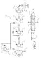
- FIG. 5illustrates one exemplary schematic diagram 500 suitable for implementing the block diagram of FIG. 4 . It will be clear to those of ordinary skill in the art having the benefit of this disclosure that any number of circuits can be created to execute the steps of receiving a signal from a touch-sensitive interface ( 201 ) and injecting ( 337 ) charge synchronously back into (or sinking charge out of) the touch-sensitive interface ( 201 ) after applying a predetermined gain.
- the schematic diagram 500 of FIG. 5is but one realization, and is not intended to be limiting.
- the circuit of FIG. 5employs a hex-buffer integrated circuit that includes six buffer/converters (inverters).
- a bufferis the MC74HCU04A Hex Unbuffered Inverter manufactured by ON Semiconductor.
- Anotheris the M54HC4049 RAD-Hard Hex Buffer/Converter manufactured by ST Microelectronics.
- Other similar hex-buffersare manufactured by Fairchild Semiconductor, Toshiba Semiconductor, and R&E International.
- the first electrode 501is coupled to a first inverter 551 .
- a second inverter 552also coupled to the input of the first inverter 551 , is biased at the toggle voltage of the first inverter 551 .
- This configurationallows the first inverter 551 to toggle from an active low state to an active high state, or vice versa, in response to very small signals that the first electrode 501 receives.
- the periodic waveform ( 307 ) emitted by touch-sensitive interfaces ( 201 )are generally periodic waves with frequencies of between 100 kHz and 200 kHz.
- the amplitude of such signals, which are capacitively-coupled through the touch-sensitive interface ( 201 ) to an electronic circuit,is often on the order of 50 mV. Accordingly, biasing the second inverter 552 at the “trip point” of the first inverter 551 can be advantageous in ensuring that the first inverter 551 toggles when the first electrode 501 receives these high frequency, small magnitude signals.
- the shroud electrode 502is coupled to a common node 553 of the circuit.
- This common node 553sometimes referred to as a “local return,” is the node to which the voltage source 554 is referenced.
- each of the buffers 551 , 552is accordingly coupled both to the voltage source 554 and the common node 553 .
- the shroud electrode 502performs two functions. First, it provides a reference against which the potential difference between the center electrode 501 and the shroud electrode 502 can be “yanked around” by the buffers to inject ( 337 ) charge into the touch-sensitive interface ( 201 ). Second, it shields the first electrode 501 from external noise sources.
- the series string of inverters 551 , 555 , 556 , 557provide a circuit equivalent to the buffer ( 441 ) shown in FIG. 4 .
- the first electrode 501is the input of the series string, and the output 558 is coupled to the stylus body ( 404 ) and then through circuit 534 to earth ground by way of the user's hand ( 203 ).
- This series string“clamps” the output to the rails provided by the voltage source 554 and the common node 553 . Whether the output 558 of the series string is active high or active low will depend upon whether the first electrode 501 is detecting a falling edge or a rising edge.
- the first inverter 551toggles. This causes the output 558 to be pulled active high. Since a user ( 202 ) is holding the stylus body ( 404 ) with his hand ( 203 ) the common node 553 is pulled down by way of circuit 534 . To the touch-sensitive interface ( 201 ), this looks like a large negative edge at the shroud electrode 502 . This synchronous “pulling down” of the common node 553 introduces the Miller capacitance ( 336 ) between the compound tip 505 and the touch-sensitive interface ( 201 ), and further increases the effective capacitance presented by the compound tip 505 to the touch-sensitive interface ( 201 ). In short, the effect is that the touch-sensitive interface ( 201 ) detects a touch, despite the fact that the compound tip 505 is significantly smaller than a user's finger.
- a first optional componentis a timer 560 .
- the timer 560can be used to power-down the circuit after a predetermined time.
- the voltage source 554is a battery
- the timer 560is configured to start timing upon use and reset with each subsequent use. Accordingly, when the user ( 202 ) stops using the stylus, and the timer 560 has expired, the circuit can be placed into a low-power or sleep mode.
- the timer 560can be configured to respond to electric field variations detected by the center electrode 501 .
- the timer 560may be configured to place the circuit into a low power or sleep mode upon non-detections of the electric field variations at the center electrode 501 for at least a predetermined time threshold.
- a second optional componentis a coding modulator 561 .
- the injected signalcan be a replication of the detected signal. Alternatively, some rising or falling edges can be ignored to provide a characteristic identifier to the touch-sensitive interface.
- a coding modulator 561can be included such that the circuit injects charge in accordance with a rolling code signal.
- a third optional componentis the force sensor 562 , one embodiment of which was described with reference to FIG. 3 (force sensor 350 ).
- the compound tip 505can transmit signals, in some embodiments it can further serve as a type of electronic key that transmits rolling codes.
- the circuitresponds to a pair of adjacent rising and falling edges by injecting ( 337 ) a negative charge in response to the rising edge, and a positive charge in response to the falling edge, so as to indicate a binary “1.”
- the coding modulator 561can cause the circuit to ignore an adjacent rising and falling edge.
- the received signalfunctions like a “clock” signal, while the charge injection signal from the compound tip 505 serves as a “data” signal.
- the data signalcan be used to unlock applications presented on the touch-sensitive interface ( 201 ).
- the coding modulator 561can be configured to function only selectively, such as when the user ( 202 ) presses a button disposed along the stylus body ( 404 ).
- FIG. 6illustrates one method 600 for interacting with a touch-sensitive interface by injecting charge into (or sinking charge from) the interface in accordance with one or more embodiments of the invention.
- the functions of the various stepshave been generally described above. Accordingly, each step will be only briefly described here.
- a receive electrode in a compound tip of a stylusdetects electric field variations emitted by the touch-sensitive interface.
- an active circuitapplies a gain to a signal corresponding to the detected electric field variations.
- a transmit electrodeinjects charge into, or sinks charge from, the touch-sensitive interface. In one embodiment, this step 605 occurs synchronously with the signal corresponding to the detected electric field variations. In one embodiment, the active circuit accomplishes this by altering an electric field defined between the receive electrode and the transmit electrode. In one embodiment, the active circuit first inverts the signal corresponding to the detected electric field variations with the active circuit, and then applies a gain.
- other inputscan be used to alter the gain applied by the active circuit. Whether optional components providing other inputs are included is determined at decision 603 . Where they are, the active circuit can alter the gain in response to these inputs at step 604 . Examples of other inputs include a force signal 606 generated by a force detector operable with the compound tip and an identification code 607 from a coding modulator.
- FIGS. 7 and 8illustrate the charge detected by a stylus that does not include an active circuit coming into contact with a touch-sensitive interface, and a stylus configured in accordance with embodiments of the present invention, respectively.
- horizontal axes 702 , 703 and 802 , 803represent the planar surface area of a touch-sensitive surface
- the vertical axes 704 , 804represent the magnitude of detection signals along that planar surface area.
- FIG. 7shows a charge detection peak 701 of the latter, i.e., a fine-tipped stylus having no active circuit.
- Examples of prior art passive stylusesinclude the Pogo Stylus manufactured by Ten-1 and the DAGi stylus manufactured by DAGi Corporation. These passive devices provide small touch-signals, similar to that shown in FIG. 7 . The actual signal delivered will change some based upon the width of the stylus tip.
- the charge detection peak 801 of embodiments of the present inventionis shown in FIG. 8 . As shown, it is orders of magnitude higher than those presented by passive prior art styluses. Further, the compound tip of embodiments of the present invention can be configured as a finer point, such as with a 2.5-millimeter center electrode, thereby resembling a ballpoint pen.
- Embodiments of the present inventionemploy a simple, active circuit that requires no alteration to the electronic device with which the stylus is used. Further, embodiments of the present invention work with a wide variety of touch-sensitive systems universally. No hardware or software alteration is required in the touch-sensitive system. Accordingly, embodiments of the present invention provide seamless transitions between finger-based input and stylus-based input. Further, embodiments of the present invention employ very few circuit components and can be manufactured robustly and inexpensively.
- FIG. 9illustrates an alternate active circuit 903 configured in accordance with embodiments of the invention.
- the active circuit 903is configured as a gyrator.
- a gyratorcan be thought of as a two-port device that couples current on one port to the voltage on the other port, and vice versa.
- the gyratorinverts and magnifies detected signals for charge injection, and is well suited to work with continuous touch-sensitive interface detection waveforms, such as sine waves.
- the suppression shroud 990is concentrically disposed about the center electrode 901 between the center electrode 901 and the shroud electrode 902 . Further, in one embodiment the suppression shroud 990 is electrically isolated from each of the center electrode 901 and the shroud electrode 902 .
- the suppression shroud 990can be electrically coupled to the common node 953 of the active circuit 903 . Circuit 999 illustrates the relationship between the common node 953 and ground 998 . Specifically, capacitive coupling 997 through a user or other object provides a return path between the common node 953 and ground 998 .
- Some capacitive touch-sensitive systemsuse discontinuous waveforms to perform capacitive measurements. Such systems are susceptible to electrical noise that also contains discontinuous waveforms. Examples of electrical noise include the common-mode noise produced by a battery charger, which is frequently included in an electronic device.
- the suppression shroud 990works to reduce the detection of the extraneous noise by the center electrode 901 .
- suppression shroud 990Another function of the suppression shroud 990 is the prevention of negative feedback occurring between the shroud electrode 902 and the center electrode 901 . Such negative feedback can work to sabotage the gain applied to the received signal at the output of the active circuit 903 .
- the suppression shroud 990can function in a manner analogous to the operation of a “screen grid” found in Tetrode and Pentode vacuum tubes. The screen grid worked to block Miller capacitance established between the control grid and the plate in these vacuum tubes.
- three capacitors 991 , 992 , 993 of the “gyrator”define a negative feedback loop about buffer 994 .
- these capacitors 991 , 992 , 993establish gain.
- capacitors 991 , 993establish a first gain for signals of the center electrode 901 relative to the suppression shroud 990
- capacitors 992 , 993define a gain for signals of the center electrode relative to the shroud electrode 902 .
- the capacitors 991 , 992 , 993work to invert the current-voltage characteristic of the active circuit 903 , thereby causing a “one-way” reversal of signal polarity. Said differently, the capacitors 991 , 992 , 993 cause a reversal of signal polarity for signals detected by the center electrode 901 , but not for either the shroud electrode 902 or the suppression shroud 990 .
- FIGS. 10 and 11illustrate optional features that can be incorporated into various embodiments of the invention.
- the compound tip 1005can be configured to be retractable.
- a push-button 1010can be provided along the stylus body 1004 .
- the push-button 1010functions as a mechanical retraction mechanism operable with the compound tip to selectively retract the compound tip within the stylus body 1004 .
- the push-buttoncan be configured to retract only the center electrode within the shroud electrode.
- the center electrode 1001when the push-button 1010 is in a first state 1011 , the center electrode 1001 is retracted within the stylus body 1004 .
- the center electrode 1001extends distally from the stylus body 1004 .
- the stylusresembles a ballpoint pen in that the center electrode 1001 can be extended when in use, but retracted otherwise.
- the push-button 1010can also be used as a power switch that disconnects the battery or other voltage source from the active circuit.
- FIG. 11illustrated therein is a stylus 1100 having compound tips 1105 , 1115 at both ends.
- the configuration of FIG. 11permits the second compound tip 1115 to respond differently from the first compound tip 1105 .
- the first compound tip 1105injects charge upon detecting a rising transition
- the second compound tip 1115may withdraw charge on rising transitions.
- the first compound tip 1105may respond to every transition, the second compound tip 1115 may respond to only positive transitions.
- the touch-sensitive interfacecan identify the different ends of the stylus 1100 . Accordingly, different features can be delivered by the different end, such as a writing tool at the first end and an eraser at the other.
- “gloved hand” operationis generally not supported by most touch-sensitive interfaces.
- the various styluses described hereinpermit gloved-hand operation.
- embodiments of the inventioncould also be configured as thimbles suitable for user wear under a glove, for incorporation into one or more fingertips of a glove, or other configurations.
- embodiments described hereinincrease capacitive coupling—even when the user is wearing gloves—so that the touch-sensitive interface can detect touches of the stylus.
- embodiments of the present inventionprovide stylus interaction that appears, to the touch-sensitive interface, as a “finger touch.”
- the styluses described hereincan be used in conjunction with fingers to perform multi-finger gesture operations.
Landscapes
- Engineering & Computer Science (AREA)
- General Engineering & Computer Science (AREA)
- Theoretical Computer Science (AREA)
- Human Computer Interaction (AREA)
- Physics & Mathematics (AREA)
- General Physics & Mathematics (AREA)
- Position Input By Displaying (AREA)
- Electronic Switches (AREA)
Abstract
Description
Claims (19)
Priority Applications (4)
| Application Number | Priority Date | Filing Date | Title |
|---|---|---|---|
| US12/974,252US8766954B2 (en) | 2010-12-21 | 2010-12-21 | Active stylus for use with touch-sensitive interfaces and corresponding method |
| PCT/US2011/065713WO2012087858A1 (en) | 2010-12-21 | 2011-12-19 | Active stylus for use with touch-sensitive interfaces and corresponding method |
| CN201180061916.2ACN103329073B (en) | 2010-12-21 | 2011-12-19 | Active stylus for use with touch-sensitive interface and corresponding method |
| EP11808495.3AEP2656183B1 (en) | 2010-12-21 | 2011-12-19 | Active stylus for use with touch-sensitive interfaces and corresponding method |
Applications Claiming Priority (1)
| Application Number | Priority Date | Filing Date | Title |
|---|---|---|---|
| US12/974,252US8766954B2 (en) | 2010-12-21 | 2010-12-21 | Active stylus for use with touch-sensitive interfaces and corresponding method |
Publications (2)
| Publication Number | Publication Date |
|---|---|
| US20120154340A1 US20120154340A1 (en) | 2012-06-21 |
| US8766954B2true US8766954B2 (en) | 2014-07-01 |
Family
ID=45478551
Family Applications (1)
| Application Number | Title | Priority Date | Filing Date |
|---|---|---|---|
| US12/974,252Expired - Fee RelatedUS8766954B2 (en) | 2010-12-21 | 2010-12-21 | Active stylus for use with touch-sensitive interfaces and corresponding method |
Country Status (4)
| Country | Link |
|---|---|
| US (1) | US8766954B2 (en) |
| EP (1) | EP2656183B1 (en) |
| CN (1) | CN103329073B (en) |
| WO (1) | WO2012087858A1 (en) |
Cited By (19)
| Publication number | Priority date | Publication date | Assignee | Title |
|---|---|---|---|---|
| US20150205391A1 (en)* | 2014-01-17 | 2015-07-23 | Egalax_Empia Technology Inc. | Active stylus having switching function |
| US20160018906A1 (en)* | 2013-03-15 | 2016-01-21 | Stacey Gottlieb | Fingernail System for Use with Capacitive Touchscreens |
| WO2016094564A1 (en)* | 2014-12-09 | 2016-06-16 | Cirque Corporation | Paint brush capacitive stylus tip |
| US9417738B2 (en) | 2009-06-12 | 2016-08-16 | Synaptics Incorporated | Untethered active pen and a method for communicating with a capacitive sensing device using the untethered active pen |
| EP3153959A2 (en) | 2015-10-09 | 2017-04-12 | Wacom Co., Ltd. | Position indicator |
| US20170262122A1 (en)* | 2016-03-08 | 2017-09-14 | Egalax_Empia Technology Inc. | Touch control apparatus for detecting tilt angle and axial direction of stylus and control method thereof |
| US9874966B2 (en) | 2015-04-28 | 2018-01-23 | Microsoft Technology Licensing, Llc | Electrostatic device having spaced electrodes |
| US20180046272A1 (en)* | 2015-05-21 | 2018-02-15 | Wacom Co., Ltd. | Active stylus |
| US10019079B2 (en) | 2014-12-07 | 2018-07-10 | Microsoft Technology Licensing, Llc | Stylus for operating a digitizer system |
| US10025403B2 (en) | 2016-07-25 | 2018-07-17 | Microsoft Technology Licensing, Llc | Stylus communication channels |
| US10359869B2 (en) | 2016-03-28 | 2019-07-23 | Samsung Electronics Co., Ltd | Stylus pen, electronic apparatus for receiving signal from stylus pen, and control method thereof |
| US20190384424A1 (en)* | 2016-06-09 | 2019-12-19 | Wacom Co., Ltd. | Active stylus with multiple sensors for receiving signals from a touch sensor |
| US10572063B2 (en) | 2017-01-09 | 2020-02-25 | Microsoft Technology Licensing, Llc | Position, tilt, and twist detection for stylus |
| US10579169B2 (en) | 2016-03-08 | 2020-03-03 | Egalax_Empia Technology Inc. | Stylus and touch control apparatus for detecting tilt angle of stylus and control method thereof |
| US10732695B2 (en) | 2018-09-09 | 2020-08-04 | Microsoft Technology Licensing, Llc | Transitioning a computing device from a low power state based on sensor input of a pen device |
| US10895928B1 (en)* | 2012-01-06 | 2021-01-19 | Steve Dabell | Method and apparatus for emulating touch and gesture events on a capacitive touch sensor |
| US11016586B2 (en)* | 2015-04-20 | 2021-05-25 | Wacom Co., Ltd. | Method using active stylus and sensor controller, sensor controller, and active stylus |
| US11269428B2 (en) | 2018-09-09 | 2022-03-08 | Microsoft Technology Licensing, Llc | Changing a mode of operation of a computing device by a pen device |
| US12229372B2 (en)* | 2011-04-11 | 2025-02-18 | Wacom Co., Ltd. | Position pointer |
Families Citing this family (111)
| Publication number | Priority date | Publication date | Assignee | Title |
|---|---|---|---|---|
| WO2010118313A1 (en)* | 2009-04-10 | 2010-10-14 | Immerz Inc. | Systems and methods for acousto-haptic speakers |
| US9310923B2 (en) | 2010-12-03 | 2016-04-12 | Apple Inc. | Input device for touch sensitive devices |
| US8638320B2 (en)* | 2011-06-22 | 2014-01-28 | Apple Inc. | Stylus orientation detection |
| US8928635B2 (en) | 2011-06-22 | 2015-01-06 | Apple Inc. | Active stylus |
| US9329703B2 (en) | 2011-06-22 | 2016-05-03 | Apple Inc. | Intelligent stylus |
| US9104251B1 (en)* | 2011-07-27 | 2015-08-11 | Cypress Semiconductor Corporation | Full-bridge tip driver for active stylus |
| US9507441B2 (en)* | 2011-09-08 | 2016-11-29 | Jcm Electronic Stylus Llc | Electronic stylus with low skew tip for capacitive touch screens |
| US9110523B2 (en) | 2011-09-08 | 2015-08-18 | JCM Electronics Stylus, LLC | Stylus and stylus circuitry for capacitive touch screens |
| US9182856B2 (en)* | 2011-10-28 | 2015-11-10 | Atmel Corporation | Capacitive force sensor |
| US9557833B2 (en)* | 2011-10-28 | 2017-01-31 | Atmel Corporation | Dynamic adjustment of received signal threshold in an active stylus |
| US10725564B2 (en)* | 2011-10-28 | 2020-07-28 | Wacom Co., Ltd. | Differential sensing in an active stylus |
| US9086745B2 (en)* | 2011-10-28 | 2015-07-21 | Atmel Corporation | Dynamic reconfiguration of electrodes in an active stylus |
| US10082889B2 (en) | 2011-10-28 | 2018-09-25 | Atmel Corporation | Multi-electrode active stylus tip |
| CN103105956B (en)* | 2011-11-11 | 2015-05-06 | 汉王科技股份有限公司 | Position indicating device and position indicating method |
| WO2013132486A1 (en)* | 2012-03-06 | 2013-09-12 | N-Trig Ltd. | Digitizer system |
| KR101335892B1 (en)* | 2012-04-23 | 2013-12-02 | 한국과학기술원 | Signal detecting system of multi wide capacitive touch-screen |
| EP2856289A4 (en) | 2012-05-25 | 2016-01-06 | Immerz Inc | Haptic interface for portable electronic device |
| US9857889B2 (en)* | 2012-06-29 | 2018-01-02 | Samsung Electronic Co., Ltd | Method and device for handling event invocation using a stylus pen |
| US20140011164A1 (en)* | 2012-07-09 | 2014-01-09 | Vtech Electronics, Ltd. | Drawing toy with stylus detection |
| US9176604B2 (en)* | 2012-07-27 | 2015-11-03 | Apple Inc. | Stylus device |
| US20140028635A1 (en)* | 2012-07-27 | 2014-01-30 | Christoph Horst Krah | Modular stylus device |
| US9557845B2 (en) | 2012-07-27 | 2017-01-31 | Apple Inc. | Input device for and method of communication with capacitive devices through frequency variation |
| US9652090B2 (en) | 2012-07-27 | 2017-05-16 | Apple Inc. | Device for digital communication through capacitive coupling |
| JP6021174B2 (en)* | 2012-08-08 | 2016-11-09 | 株式会社ワコム | Position detecting device and position indicator thereof |
| US9563304B2 (en)* | 2012-08-15 | 2017-02-07 | Atmel Corporation | Active stylus with passive mutual measurements |
| GB2519475A (en)* | 2012-08-21 | 2015-04-22 | Immerz Inc | Systems and methods for a vibrating input device |
| US9921626B2 (en)* | 2012-09-28 | 2018-03-20 | Atmel Corporation | Stylus communication with near-field coupling |
| US10031590B2 (en)* | 2012-10-16 | 2018-07-24 | Atmel Corporation | Active stylus with a parallel communication channel |
| EP2743798A1 (en)* | 2012-12-13 | 2014-06-18 | BlackBerry Limited | Magnetically coupling stylus and host electronic device |
| CN103984422B (en)* | 2013-02-08 | 2017-06-16 | 汉王科技股份有限公司 | Capacitive pen, capacitive touch panel and touch device |
| WO2014127383A2 (en)* | 2013-02-17 | 2014-08-21 | Zeliff Zachary Joseph | Stylus for capacitive touchscreen |
| WO2014130355A2 (en)* | 2013-02-19 | 2014-08-28 | Jcm Electronic Stylus Llc | Electronic stylus with low skew tip for capacitive touch screens |
| US10048775B2 (en) | 2013-03-14 | 2018-08-14 | Apple Inc. | Stylus detection and demodulation |
| US9035919B2 (en)* | 2013-03-15 | 2015-05-19 | Microchip Technology Incorporated | Electrostatics stylus |
| US9256330B2 (en)* | 2013-05-22 | 2016-02-09 | Qualcomm Technologies, Inc. | Capacitive touch panel configured to sense both active and passive input with a single sensor |
| FR3006461B1 (en) | 2013-05-29 | 2015-06-05 | Bic Soc | MANUAL DEVICE COMPRISING AN INVERTER CAP FOR A CAPACITIVE SCREEN |
| TWI628576B (en)* | 2013-06-03 | 2018-07-01 | 蕭景中 | Active capacitive touch device |
| KR101489813B1 (en)* | 2013-06-28 | 2015-02-04 | 삼성전기주식회사 | Touch panel including Active stylus pen and controlling method thereof |
| DE102013214021A1 (en)* | 2013-07-17 | 2015-01-22 | Stabilo International Gmbh | power savings |
| WO2015013537A2 (en)* | 2013-07-24 | 2015-01-29 | FiftyThree, Inc. | Stylus having a deformable tip and methods of using the same |
| WO2015013533A2 (en)* | 2013-07-24 | 2015-01-29 | FiftyThree, Inc. | Methods and apparatus for implementing dual tip functionality in a stylus device |
| US10067580B2 (en) | 2013-07-31 | 2018-09-04 | Apple Inc. | Active stylus for use with touch controller architecture |
| CN103455176B (en)* | 2013-08-16 | 2017-05-24 | 汉王科技股份有限公司 | Active capacitance pen, capacitance touch panel and touch device |
| US9785263B2 (en) | 2013-08-22 | 2017-10-10 | Microchip Technology Incorporated | Touch screen stylus with force and/or angle sensing functionality |
| KR102135678B1 (en)* | 2013-09-27 | 2020-07-20 | 삼성전자주식회사 | Auxiliary device having energy harvester and electronic device including the auxiliary device |
| TWI536208B (en)* | 2013-10-02 | 2016-06-01 | 翰碩電子股份有限公司 | Active capacitive touch pen |
| US9395824B2 (en)* | 2013-10-18 | 2016-07-19 | Synaptics Incorporated | Active pen with improved interference performance |
| CN108279815B (en)* | 2013-11-08 | 2020-07-07 | 禾瑞亚科技股份有限公司 | Transmitter and its position detection and calculation method, touch processing device and system |
| US9298285B2 (en)* | 2013-12-05 | 2016-03-29 | Wacom Co., Ltd. | Stylus tip shape |
| US9436325B2 (en) | 2013-12-20 | 2016-09-06 | Synaptics Incorporated | Active pen for matrix sensor |
| CN103729073B (en)* | 2013-12-20 | 2016-07-06 | 艾攀科技有限公司 | Active capacitance pen |
| US10055033B2 (en) | 2013-12-23 | 2018-08-21 | Shanghai Yishang Information Technology Co., Ltd. | Active capacitive pen, and touch detection and feedback driving methods therefor |
| TWI526917B (en)* | 2014-03-24 | 2016-03-21 | 義隆電子股份有限公司 | Capacitive touch device and method for simultaneously detecting active stylus and object on capacitive touch device |
| JP6304814B2 (en) | 2014-05-23 | 2018-04-04 | 株式会社ワコム | Position detecting device and position indicator |
| CN104077001B (en)* | 2014-06-19 | 2017-04-12 | 艾攀科技有限公司 | A method for identifying touch screen contact objects and a method for transmitting signals by a capacitive pen |
| WO2015200396A1 (en)* | 2014-06-27 | 2015-12-30 | 3M Innovative Properties Company | Touch systems stylus and methods |
| CN106796459B (en)* | 2014-07-31 | 2020-09-18 | 惠普发展公司,有限责任合伙企业 | Touch pen |
| US9569016B2 (en)* | 2014-08-18 | 2017-02-14 | Atmel Corporation | Low-power and low-frequency data transmission for stylus |
| US9798396B2 (en)* | 2014-08-18 | 2017-10-24 | Atmel Corporation | Low-power and low-frequency data transmission for stylus and associated signal processing |
| US11079862B2 (en) | 2014-08-18 | 2021-08-03 | Wacom Co., Ltd. | Low-power and low-frequency data transmission for stylus and associated signal processing |
| US10331284B2 (en)* | 2014-10-08 | 2019-06-25 | Generalplus Technology Inc. | Touch-control communication system and touch-control communication method |
| FR3028629B1 (en) | 2014-11-19 | 2017-01-27 | SOCIéTé BIC | MANUAL DEVICE COMPRISING AN INVERTER CAP FOR A CAPACITIVE SCREEN |
| US10180736B2 (en)* | 2014-11-26 | 2019-01-15 | Synaptics Incorporated | Pen with inductor |
| US10067618B2 (en) | 2014-12-04 | 2018-09-04 | Apple Inc. | Coarse scan and targeted active mode scan for touch |
| US9830000B2 (en)* | 2014-12-12 | 2017-11-28 | Microsoft Technology Licensing, Llc | Active stylus synchronization |
| US10175827B2 (en) | 2014-12-23 | 2019-01-08 | Synaptics Incorporated | Detecting an active pen using a capacitive sensing device |
| KR102310484B1 (en)* | 2014-12-31 | 2021-10-08 | 엘지디스플레이 주식회사 | Touch screen device |
| KR102260600B1 (en)* | 2014-12-31 | 2021-06-04 | 엘지디스플레이 주식회사 | Touch screen device |
| CN107209599B (en)* | 2015-02-09 | 2020-10-16 | 株式会社和冠 | Communication method, communication system, sensor controller and touch pen |
| US9977519B2 (en)* | 2015-02-25 | 2018-05-22 | Synaptics Incorporated | Active pen with bidirectional communication |
| TWI574178B (en)* | 2015-03-31 | 2017-03-11 | 義隆電子股份有限公司 | Active stylus and its position information correction method |
| KR102356636B1 (en) | 2015-06-26 | 2022-01-28 | 삼성전자주식회사 | Input device, electronic apparatus for receiving signal from the input device and controlling method thereof |
| EP3314380A4 (en)* | 2015-06-26 | 2018-08-22 | Samsung Electronics Co., Ltd. | Input device, electronic device for receiving signal from input device, and control method thereof |
| US9720546B2 (en) | 2015-09-15 | 2017-08-01 | Microsoft Technology Licensing, Llc | Calibration of a force sensitive device |
| US10037111B2 (en)* | 2015-09-16 | 2018-07-31 | Synaptics Incorporated | Single point charger |
| US10037112B2 (en) | 2015-09-30 | 2018-07-31 | Synaptics Incorporated | Sensing an active device'S transmission using timing interleaved with display updates |
| DE102015219484A1 (en)* | 2015-10-08 | 2017-04-13 | Stabilo International Gmbh | Energy savings in a pointing instrument for capacitive sensor surfaces by temporal modulation |
| DE202015105327U1 (en)* | 2015-10-08 | 2017-01-11 | Stabilo International Gmbh | Energy savings in a pointing instrument for capacitive sensor surfaces by temporal modulation |
| DE102015219487A1 (en)* | 2015-10-08 | 2017-04-13 | Stabilo International Gmbh | Energy savings in a pointing instrument for capacitive sensor surfaces by inclination measurement |
| DE102015219494A1 (en)* | 2015-10-08 | 2017-04-13 | Stabilo International Gmbh | Pointing instrument for capacitive sensor surfaces with ultrasonic control |
| DE102015220811A1 (en)* | 2015-10-23 | 2017-04-27 | Stabilo International Gmbh | Pencil with thin tip for capacitive touch fields |
| DE102015220814A1 (en)* | 2015-10-23 | 2017-04-27 | Stabilo International Gmbh | Active stylus for capacitive sensor surfaces with hand recognition |
| DE202015105664U1 (en)* | 2015-10-23 | 2017-01-24 | Stabilo International Gmbh | Pencil with thin tip for capacitive touch fields |
| FR3042887B1 (en) | 2015-10-27 | 2017-11-17 | SOCIéTé BIC | RETRACTABLE POINT WRITING INSTRUMENT COMPRISING CAPACITIVE SHIELD CUSHION |
| TWI592835B (en)* | 2016-01-14 | 2017-07-21 | 明基電通股份有限公司 | Interactive system and related handheld components that can switch between different writing modes |
| US9965056B2 (en) | 2016-03-02 | 2018-05-08 | FiftyThree, Inc. | Active stylus and control circuit thereof |
| US10254857B2 (en) | 2016-03-06 | 2019-04-09 | Microsoft Technology Licensing, Llc | Soft touch detection of a stylus |
| US10514803B2 (en)* | 2016-03-06 | 2019-12-24 | Microsoft Technology Licensing, Llc | Pen in field force sensing calibration |
| KR102523154B1 (en)* | 2016-04-22 | 2023-04-21 | 삼성전자주식회사 | Display apparatus, input device and control method thereof |
| US9891724B2 (en)* | 2016-05-04 | 2018-02-13 | Adonit Co., Ltd. | Circuit and stylus for capacitive touchscreen |
| US10474277B2 (en) | 2016-05-31 | 2019-11-12 | Apple Inc. | Position-based stylus communication |
| WO2018081939A1 (en) | 2016-11-02 | 2018-05-11 | 深圳市汇顶科技股份有限公司 | Method for determining target working frequency of stylus, touchscreen, and stylus |
| TWI608385B (en)* | 2016-12-16 | 2017-12-11 | 矽統科技股份有限公司 | Active stylus |
| US10797697B2 (en)* | 2017-08-02 | 2020-10-06 | Tactual Labs Co. | Phase relationship sensing system |
| TWI630513B (en)* | 2017-08-04 | 2018-07-21 | Waltop International Corporation | Capacitive stylus providing signals for tilt and orientation detection |
| CN109683730A (en)* | 2017-10-18 | 2019-04-26 | 中强光电股份有限公司 | Stylus and touch-control system with it |
| TWI697814B (en)* | 2018-07-16 | 2020-07-01 | 禾瑞亞科技股份有限公司 | Functional modular touch pen |
| WO2020023640A1 (en)* | 2018-07-24 | 2020-01-30 | Shapirten Laboratories Llc | Power efficient stylus for an electronic device |
| CN109766018B (en)* | 2019-01-16 | 2022-03-01 | 深圳市绘王动漫科技有限公司 | Active capacitance pen and gain feedback control method thereof |
| WO2021022552A1 (en)* | 2019-08-08 | 2021-02-11 | 深圳市汇顶科技股份有限公司 | Signal driving circuit generating positive and negative voltages, chip, active pen, and signal driving method |
| US11449175B2 (en) | 2020-03-31 | 2022-09-20 | Apple Inc. | System and method for multi-frequency projection scan for input device detection |
| CN115552361A (en) | 2020-03-31 | 2022-12-30 | 夏皮滕实验室有限责任公司 | Electrostatic discharge protection for high-efficiency stylus for electronic devices |
| US11243619B2 (en) | 2020-06-30 | 2022-02-08 | Dell Products L.P. | Information handling system stylus with integrated push button and charging port |
| EP4204933A1 (en) | 2020-08-27 | 2023-07-05 | Shapirten Laboratories Llc | Mechanically sensitive power efficient stylus for an electronic device |
| US11460933B2 (en) | 2020-09-24 | 2022-10-04 | Apple Inc. | Shield electrode for input device |
| US11997777B2 (en) | 2020-09-24 | 2024-05-28 | Apple Inc. | Electrostatic discharge robust design for input device |
| US11287926B1 (en) | 2020-09-25 | 2022-03-29 | Apple Inc. | System and machine learning method for detecting input device distance from touch sensitive surfaces |
| US11526240B1 (en) | 2020-09-25 | 2022-12-13 | Apple Inc. | Reducing sensitivity to leakage variation for passive stylus |
| US12153764B1 (en) | 2020-09-25 | 2024-11-26 | Apple Inc. | Stylus with receive architecture for position determination |
| CN113220144B (en)* | 2021-03-15 | 2022-06-07 | 荣耀终端有限公司 | Stylus |
| US12242695B1 (en) | 2022-09-06 | 2025-03-04 | Apple Inc. | System and method for stylus detection |
Citations (60)
| Publication number | Priority date | Publication date | Assignee | Title |
|---|---|---|---|---|
| US4076428A (en) | 1975-05-15 | 1978-02-28 | Tokyo Boshi Kabushiki Kaisha | Pen points for writing instruments |
| US4654648A (en) | 1984-12-17 | 1987-03-31 | Herrington Richard A | Wireless cursor control system |
| US4672154A (en) | 1985-04-03 | 1987-06-09 | Kurta Corporation | Low power, high resolution digitizing system with cordless pen/mouse |
| US5528002A (en)* | 1993-07-15 | 1996-06-18 | Pentel Kabushiki Kaisha | Noiseproof digitizing apparatus with low power cordless pen |
| US5693914A (en) | 1995-02-28 | 1997-12-02 | Wacom Co., Ltd. | Digitizer and method of detecting positions |
| US5828011A (en)* | 1994-02-04 | 1998-10-27 | At&T Global Information Solutions Company | High voltage stylus for portable computer |
| US5913629A (en) | 1998-05-07 | 1999-06-22 | Ttools, Llc | Writing implement including an input stylus |
| US6050490A (en) | 1997-10-31 | 2000-04-18 | Hewlett-Packard Company | Handheld writing device and related data entry system |
| US6133906A (en) | 1993-03-15 | 2000-10-17 | Microtouch Systems, Inc. | Display-integrated stylus detection system |
| US6175773B1 (en) | 1987-10-19 | 2001-01-16 | Lg Electronics, Inc. | High resolution system for sensing spatial coordinates |
| US20020040817A1 (en) | 2000-10-06 | 2002-04-11 | International Business Machines Corporation | Data steering flip pen system |
| US6396481B1 (en) | 1999-04-19 | 2002-05-28 | Ecrio Inc. | Apparatus and method for portable handwriting capture |
| WO2002058029A2 (en) | 2000-11-29 | 2002-07-25 | Sekendur Oral F | Optical position determination on any surface |
| US6450721B1 (en) | 2001-08-17 | 2002-09-17 | A.T.X. International, Inc. | Stylus and retractable pen |
| US6473072B1 (en)* | 1998-05-12 | 2002-10-29 | E Ink Corporation | Microencapsulated electrophoretic electrostatically-addressed media for drawing device applications |
| US6550997B1 (en) | 2000-10-20 | 2003-04-22 | Silverbrook Research Pty Ltd | Printhead/ink cartridge for pen |
| US6577299B1 (en) | 1998-08-18 | 2003-06-10 | Digital Ink, Inc. | Electronic portable pen apparatus and method |
| US20030118391A1 (en) | 2001-12-14 | 2003-06-26 | Adams Guy De Warrenne Bruce | Writing implement |
| US20030164821A1 (en)* | 2002-02-05 | 2003-09-04 | Omid Rezania | Writing instrument with variable display |
| US20040041799A1 (en)* | 2001-10-16 | 2004-03-04 | Vincent Kent D. | Electronic writing and erasing pencil |
| US6749354B2 (en) | 2002-04-26 | 2004-06-15 | Kotobuki & Co., Ltd. | Composite writing implement |
| US20040201580A1 (en)* | 2003-04-09 | 2004-10-14 | Koji Fujiwara | Pen input/display device |
| US6812685B2 (en) | 2001-03-22 | 2004-11-02 | Actuant Corporation | Auto-selecting, auto-ranging contact/noncontact voltage and continuity tester |
| US20050051550A1 (en) | 2003-09-04 | 2005-03-10 | Hiroyuki Hagano | Fuel cap |
| US6867765B2 (en) | 2000-10-06 | 2005-03-15 | International Business Machines Corporation | Use of a paper pad with uniquely identified pages in a digitizer system |
| US20050122319A1 (en)* | 2003-12-08 | 2005-06-09 | Fujitsu Component Limited | Input pen and input device |
| US20060227121A1 (en) | 2005-03-30 | 2006-10-12 | Microsoft Corporation | Systems and methods for providing a dual mode input device in a computing system |
| US20060244738A1 (en) | 2005-04-29 | 2006-11-02 | Nishimura Ken A | Pen input device and method for tracking pen position |
| US20070025805A1 (en) | 2005-08-01 | 2007-02-01 | Silverbrook Research Pty Ltd | Pen with side loading cartridge |
| US7236161B2 (en) | 2003-03-21 | 2007-06-26 | 3M Innovative Properties Company | Remote touch simulation systems and methods |
| US20070146351A1 (en)* | 2005-12-12 | 2007-06-28 | Yuji Katsurahira | Position input device and computer system |
| JP2007183809A (en) | 2006-01-06 | 2007-07-19 | Sony Corp | Stylus input device and stylus input method |
| US20070188477A1 (en)* | 2006-02-13 | 2007-08-16 | Rehm Peter H | Sketch pad and optical stylus for a personal computer |
| US20080030486A1 (en) | 2006-08-04 | 2008-02-07 | Quiteso Technologies, Llc | Multi-functional pen input device |
| US20090012806A1 (en) | 2007-06-10 | 2009-01-08 | Camillo Ricordi | System, method and apparatus for data capture and management |
| US7477242B2 (en) | 2002-05-20 | 2009-01-13 | 3M Innovative Properties Company | Capacitive touch screen with conductive polymer |
| US7483018B2 (en) | 2005-05-04 | 2009-01-27 | Microsoft Corporation | Systems and methods for providing a combined pen and mouse input device in a computing system |
| US20090027349A1 (en)* | 2007-07-26 | 2009-01-29 | Comerford Liam D | Interactive Display Device |
| US7489308B2 (en) | 2003-02-14 | 2009-02-10 | Microsoft Corporation | Determining the location of the tip of an electronic stylus |
| EP2065797A2 (en) | 2007-11-27 | 2009-06-03 | Seiko Epson Corporation | Display system, display device, and program |
| US20090183929A1 (en) | 2005-06-08 | 2009-07-23 | Guanglie Zhang | Writing system with camera |
| US7612767B1 (en) | 2005-08-24 | 2009-11-03 | Griffin Technology, Inc. | Trackpad pen for use with computer touchpad |
| US7646377B2 (en) | 2005-05-06 | 2010-01-12 | 3M Innovative Properties Company | Position digitizing using an optical stylus to image a display |
| US20100006350A1 (en) | 2008-07-11 | 2010-01-14 | Elias John G | Stylus Adapted For Low Resolution Touch Sensor Panels |
| EP2159669A2 (en) | 2008-09-01 | 2010-03-03 | E Turbotouch Technology Inc. | Electromagnetic stylus for operating a capacitive touch panel |
| US7685538B2 (en) | 2003-01-31 | 2010-03-23 | Wacom Co., Ltd. | Method of triggering functions in a computer application using a digitizer having a stylus and a digitizer system |
| US7719515B2 (en) | 2002-04-19 | 2010-05-18 | Sharp Kabushiki Kaisha | Input device and I/O-integrated display |
| US20100170726A1 (en)* | 2009-01-06 | 2010-07-08 | Elan Microelectronics Corporation | Electronic stylus, capacitive touchpad module, and apparatus for touch input |
| US20100177121A1 (en) | 2008-12-12 | 2010-07-15 | Fuminori Homma | Information processing apparatus, information processing method, and program |
| US20100315384A1 (en) | 2009-06-12 | 2010-12-16 | Kirk Hargreaves | Untethered active pen and a method for communicating with a capacitive sensing device using the untethered active pen |
| WO2011008533A2 (en) | 2009-06-29 | 2011-01-20 | Gerald Leto | Multifunctional writing apparatus with capacitive touch screen stylus |
| US20110193776A1 (en)* | 2010-02-05 | 2011-08-11 | Wacom Co., Ltd. | Pointer, position detection apparatus and position detection method |
| US8031177B2 (en) | 1999-05-25 | 2011-10-04 | Silverbrook Research Pty Ltd | Electronic pen with retractable nib |
| US20110304577A1 (en)* | 2010-06-11 | 2011-12-15 | Sp Controls, Inc. | Capacitive touch screen stylus |
| US20120050207A1 (en)* | 2010-08-30 | 2012-03-01 | Perceptive Pixel Inc. | Localizing an Electrostatic Stylus Within a Capacitive Touch Sensor |
| US20120050231A1 (en) | 2010-08-30 | 2012-03-01 | Perceptive Pixel Inc. | Systems for an Electrostatic Stylus Within a Capacitive Touch Sensor |
| US20120068964A1 (en) | 2010-09-22 | 2012-03-22 | Cypress Semiconductor Corporation | Capacitive stylus for a touch screen |
| US8217918B2 (en)* | 2002-08-29 | 2012-07-10 | N-Trig Ltd. | Transparent digitiser |
| US8226315B1 (en) | 2007-06-15 | 2012-07-24 | Marvell International Ltd. | Electronic pens with dynamic features |
| US8253702B2 (en)* | 2003-11-14 | 2012-08-28 | Wacom Co., Ltd. | Position detecting apparatus and position pointer |
Family Cites Families (1)
| Publication number | Priority date | Publication date | Assignee | Title |
|---|---|---|---|---|
| US20050156912A1 (en)* | 2003-09-12 | 2005-07-21 | Brian Taylor | Tethered stylyus for use with a capacitance-sensitive touchpad |
- 2010
- 2010-12-21USUS12/974,252patent/US8766954B2/ennot_activeExpired - Fee Related
- 2011
- 2011-12-19WOPCT/US2011/065713patent/WO2012087858A1/enactiveApplication Filing
- 2011-12-19EPEP11808495.3Apatent/EP2656183B1/enactiveActive
- 2011-12-19CNCN201180061916.2Apatent/CN103329073B/enactiveActive
Patent Citations (63)
| Publication number | Priority date | Publication date | Assignee | Title |
|---|---|---|---|---|
| US4076428A (en) | 1975-05-15 | 1978-02-28 | Tokyo Boshi Kabushiki Kaisha | Pen points for writing instruments |
| US4654648A (en) | 1984-12-17 | 1987-03-31 | Herrington Richard A | Wireless cursor control system |
| US4672154A (en) | 1985-04-03 | 1987-06-09 | Kurta Corporation | Low power, high resolution digitizing system with cordless pen/mouse |
| US6175773B1 (en) | 1987-10-19 | 2001-01-16 | Lg Electronics, Inc. | High resolution system for sensing spatial coordinates |
| US6133906A (en) | 1993-03-15 | 2000-10-17 | Microtouch Systems, Inc. | Display-integrated stylus detection system |
| US5528002A (en)* | 1993-07-15 | 1996-06-18 | Pentel Kabushiki Kaisha | Noiseproof digitizing apparatus with low power cordless pen |
| US5828011A (en)* | 1994-02-04 | 1998-10-27 | At&T Global Information Solutions Company | High voltage stylus for portable computer |
| US5693914A (en) | 1995-02-28 | 1997-12-02 | Wacom Co., Ltd. | Digitizer and method of detecting positions |
| US6050490A (en) | 1997-10-31 | 2000-04-18 | Hewlett-Packard Company | Handheld writing device and related data entry system |
| US5913629A (en) | 1998-05-07 | 1999-06-22 | Ttools, Llc | Writing implement including an input stylus |
| US6473072B1 (en)* | 1998-05-12 | 2002-10-29 | E Ink Corporation | Microencapsulated electrophoretic electrostatically-addressed media for drawing device applications |
| US6577299B1 (en) | 1998-08-18 | 2003-06-10 | Digital Ink, Inc. | Electronic portable pen apparatus and method |
| US6396481B1 (en) | 1999-04-19 | 2002-05-28 | Ecrio Inc. | Apparatus and method for portable handwriting capture |
| US8031177B2 (en) | 1999-05-25 | 2011-10-04 | Silverbrook Research Pty Ltd | Electronic pen with retractable nib |
| US20020040817A1 (en) | 2000-10-06 | 2002-04-11 | International Business Machines Corporation | Data steering flip pen system |
| US6867765B2 (en) | 2000-10-06 | 2005-03-15 | International Business Machines Corporation | Use of a paper pad with uniquely identified pages in a digitizer system |
| US6550997B1 (en) | 2000-10-20 | 2003-04-22 | Silverbrook Research Pty Ltd | Printhead/ink cartridge for pen |
| WO2002058029A2 (en) | 2000-11-29 | 2002-07-25 | Sekendur Oral F | Optical position determination on any surface |
| US6812685B2 (en) | 2001-03-22 | 2004-11-02 | Actuant Corporation | Auto-selecting, auto-ranging contact/noncontact voltage and continuity tester |
| US6450721B1 (en) | 2001-08-17 | 2002-09-17 | A.T.X. International, Inc. | Stylus and retractable pen |
| US20040041799A1 (en)* | 2001-10-16 | 2004-03-04 | Vincent Kent D. | Electronic writing and erasing pencil |
| US20030118391A1 (en) | 2001-12-14 | 2003-06-26 | Adams Guy De Warrenne Bruce | Writing implement |
| US20030164821A1 (en)* | 2002-02-05 | 2003-09-04 | Omid Rezania | Writing instrument with variable display |
| US7719515B2 (en) | 2002-04-19 | 2010-05-18 | Sharp Kabushiki Kaisha | Input device and I/O-integrated display |
| US6749354B2 (en) | 2002-04-26 | 2004-06-15 | Kotobuki & Co., Ltd. | Composite writing implement |
| US7477242B2 (en) | 2002-05-20 | 2009-01-13 | 3M Innovative Properties Company | Capacitive touch screen with conductive polymer |
| US8217918B2 (en)* | 2002-08-29 | 2012-07-10 | N-Trig Ltd. | Transparent digitiser |
| US7685538B2 (en) | 2003-01-31 | 2010-03-23 | Wacom Co., Ltd. | Method of triggering functions in a computer application using a digitizer having a stylus and a digitizer system |
| US7489308B2 (en) | 2003-02-14 | 2009-02-10 | Microsoft Corporation | Determining the location of the tip of an electronic stylus |
| US7236161B2 (en) | 2003-03-21 | 2007-06-26 | 3M Innovative Properties Company | Remote touch simulation systems and methods |
| US20040201580A1 (en)* | 2003-04-09 | 2004-10-14 | Koji Fujiwara | Pen input/display device |
| US20050051550A1 (en) | 2003-09-04 | 2005-03-10 | Hiroyuki Hagano | Fuel cap |
| US8253702B2 (en)* | 2003-11-14 | 2012-08-28 | Wacom Co., Ltd. | Position detecting apparatus and position pointer |
| US20050122319A1 (en)* | 2003-12-08 | 2005-06-09 | Fujitsu Component Limited | Input pen and input device |
| US7528825B2 (en)* | 2003-12-08 | 2009-05-05 | Fujitsu Component Limited | Input pen and input device |
| US20060227121A1 (en) | 2005-03-30 | 2006-10-12 | Microsoft Corporation | Systems and methods for providing a dual mode input device in a computing system |
| US7889186B2 (en) | 2005-04-29 | 2011-02-15 | Avago Technologies Ecbu Ip (Singapore) Pte. Ltd. | Pen input device and method for tracking pen position |
| US20060244738A1 (en) | 2005-04-29 | 2006-11-02 | Nishimura Ken A | Pen input device and method for tracking pen position |
| US7483018B2 (en) | 2005-05-04 | 2009-01-27 | Microsoft Corporation | Systems and methods for providing a combined pen and mouse input device in a computing system |
| US7646377B2 (en) | 2005-05-06 | 2010-01-12 | 3M Innovative Properties Company | Position digitizing using an optical stylus to image a display |
| US20090183929A1 (en) | 2005-06-08 | 2009-07-23 | Guanglie Zhang | Writing system with camera |
| US7794167B2 (en) | 2005-08-01 | 2010-09-14 | Silverbrook Research Pty Ltd | Pen with side loading cartridge |
| US20070025805A1 (en) | 2005-08-01 | 2007-02-01 | Silverbrook Research Pty Ltd | Pen with side loading cartridge |
| US7612767B1 (en) | 2005-08-24 | 2009-11-03 | Griffin Technology, Inc. | Trackpad pen for use with computer touchpad |
| US20070146351A1 (en)* | 2005-12-12 | 2007-06-28 | Yuji Katsurahira | Position input device and computer system |
| JP2007183809A (en) | 2006-01-06 | 2007-07-19 | Sony Corp | Stylus input device and stylus input method |
| US20070188477A1 (en)* | 2006-02-13 | 2007-08-16 | Rehm Peter H | Sketch pad and optical stylus for a personal computer |
| US20080030486A1 (en) | 2006-08-04 | 2008-02-07 | Quiteso Technologies, Llc | Multi-functional pen input device |
| US20090012806A1 (en) | 2007-06-10 | 2009-01-08 | Camillo Ricordi | System, method and apparatus for data capture and management |
| US8226315B1 (en) | 2007-06-15 | 2012-07-24 | Marvell International Ltd. | Electronic pens with dynamic features |
| US20090027349A1 (en)* | 2007-07-26 | 2009-01-29 | Comerford Liam D | Interactive Display Device |
| EP2065797A2 (en) | 2007-11-27 | 2009-06-03 | Seiko Epson Corporation | Display system, display device, and program |
| US20100006350A1 (en) | 2008-07-11 | 2010-01-14 | Elias John G | Stylus Adapted For Low Resolution Touch Sensor Panels |
| EP2159669A2 (en) | 2008-09-01 | 2010-03-03 | E Turbotouch Technology Inc. | Electromagnetic stylus for operating a capacitive touch panel |
| US20100177121A1 (en) | 2008-12-12 | 2010-07-15 | Fuminori Homma | Information processing apparatus, information processing method, and program |
| US20100170726A1 (en)* | 2009-01-06 | 2010-07-08 | Elan Microelectronics Corporation | Electronic stylus, capacitive touchpad module, and apparatus for touch input |
| US20100315384A1 (en) | 2009-06-12 | 2010-12-16 | Kirk Hargreaves | Untethered active pen and a method for communicating with a capacitive sensing device using the untethered active pen |
| WO2011008533A2 (en) | 2009-06-29 | 2011-01-20 | Gerald Leto | Multifunctional writing apparatus with capacitive touch screen stylus |
| US20110193776A1 (en)* | 2010-02-05 | 2011-08-11 | Wacom Co., Ltd. | Pointer, position detection apparatus and position detection method |
| US20110304577A1 (en)* | 2010-06-11 | 2011-12-15 | Sp Controls, Inc. | Capacitive touch screen stylus |
| US20120050207A1 (en)* | 2010-08-30 | 2012-03-01 | Perceptive Pixel Inc. | Localizing an Electrostatic Stylus Within a Capacitive Touch Sensor |
| US20120050231A1 (en) | 2010-08-30 | 2012-03-01 | Perceptive Pixel Inc. | Systems for an Electrostatic Stylus Within a Capacitive Touch Sensor |
| US20120068964A1 (en) | 2010-09-22 | 2012-03-22 | Cypress Semiconductor Corporation | Capacitive stylus for a touch screen |
Non-Patent Citations (18)
| Title |
|---|
| B&H Foto & Electronics Corp., "Targus 3-in-1 Stylus for Capacitive Devices", www.bhpotovideo.com/c/product/808841-REG/Targus-AMMO4TBUS-3-in-1-Stylus-for-Capacitive.html, downloaded from internet Mar. 20, 2012, 2 pages. |
| Dagi Corporation Ltd. "iPad Stylus" electronic catalog page, http://www.dagi.com.tw/front/bin/home.phtml, printed Aug. 23, 2011, 2 pages. |
| Dell Axim x30 Stylus with Ballpoint Pen, http://www.cel-phone-accessories.com/aximx.30.html, 2011, 1 page. |
| Fisher Spacepen, "Fisher Bullet Space Pen Stylus w/Clip-Chrome", http://www.styluscentral.com/shopexd.asp?id=200, downloaded from Internet Jun. 11, 2012, 1 page. |
| Hardcandy Cases, "CandyStylus+Pen", http://www.hardcandycases.com/candy-ipad-stylus.html, 2011, 2 pages. |
| Intellipen, "IntelliPen PRO: Digital Pen & USB Flash Drive", http://www.intellipens.com/?CategoryID=182, 2009, 2 pages. |
| Jiri Slaby et al., "Dual Mode Active Stylus for Writing Both on a Capacitive Touchscreen and Paper", U.S. Appl. No. 13/426,860, filed Mar. 22, 2012, 44 pages. |
| Kevin Purcell, "LunaTik Touch Pen Stylus-Ballpoint Pen in an iPad Stylus Tip", GottaBe Mobile: Mobile News & Reviews, www.gottabemobile.com/2011/12/13/lunatik-tough-pen-stylus-ballpoint-pen-in-an-ipad-stylus-tip/#, Dec. 13, 2011, 2 pages. |
| Mark D. Hansen et al., "Touchscreen Writing System", U.S. Appl. No. 13/450,906, filed Apr. 19, 2012, 25 pages. |
| More/Real, "Stylus Caps", http://more-real.com, downloaded from internet Mar. 20, 2012, 3 pages. |
| N-TRIG Ltd., "DuoSense Pen and Multi-Touch Solution" internet brochure, http://www.ntrig.com, downloaded from internet Jun. 11, 2012, 3 pages. |
| Patent Cooperation Treaty, "PCT Search Report and Written Opinion of the International Searching Authority" for International Application No. PCT/US2011/065713, Apr. 12, 2012, 14 pages. |
| Patent Cooperation Treaty, "PCT Search Report and Written Opinion of the International Searching Authority" for International Application No. PCT/US2013/026976, Jun. 11, 2013, 10 pages. |
| Patent Cooperation Treaty, "PCT Search Report and Written Opinion of the International Searching Authority" for International Application No. PCT/US2013/037273, Jul. 5, 2013, 12 pages. |
| Ten One Design LLC, "Pogo Stylus for iPhone & iPod touch", http://tenonedesign.com/stylus.php, 2011, 3 pages. |
| United States Patent and Trademark Office, "Non-Final Rejection" for U.S. Appl. No. 13/426,860 dated Oct. 28, 2013, 15 pages. |
| United States Patent and Trademark Office, "Non-Final Rejection" for U.S. Appl. No. 13/450,906, Jan. 13, 2014, 28 pages. |
| Wacom, "Bamboo User's Manual for Windows & Macintosh", 2009, 90 pages. |
Cited By (42)
| Publication number | Priority date | Publication date | Assignee | Title |
|---|---|---|---|---|
| US9417738B2 (en) | 2009-06-12 | 2016-08-16 | Synaptics Incorporated | Untethered active pen and a method for communicating with a capacitive sensing device using the untethered active pen |
| US20250156014A1 (en)* | 2011-04-11 | 2025-05-15 | Wacom Co., Ltd. | Position pointer |
| US12229372B2 (en)* | 2011-04-11 | 2025-02-18 | Wacom Co., Ltd. | Position pointer |
| US10895928B1 (en)* | 2012-01-06 | 2021-01-19 | Steve Dabell | Method and apparatus for emulating touch and gesture events on a capacitive touch sensor |
| US9753551B2 (en)* | 2013-03-15 | 2017-09-05 | Stacey Gottlieb | Fingernail system for use with capacitive touchscreens |
| US20160018906A1 (en)* | 2013-03-15 | 2016-01-21 | Stacey Gottlieb | Fingernail System for Use with Capacitive Touchscreens |
| US10303267B2 (en)* | 2013-03-15 | 2019-05-28 | Stacey Gottlieb | Fingernail system for use with capacitive touchscreens |
| US10025394B2 (en) | 2013-03-15 | 2018-07-17 | Stacey Gottlieb | Fingernail system for use with capacitive touchscreens |
| US9665192B2 (en)* | 2014-01-17 | 2017-05-30 | Egalax_Empia Technology Inc. | Active stylus having switching function |
| US20150205391A1 (en)* | 2014-01-17 | 2015-07-23 | Egalax_Empia Technology Inc. | Active stylus having switching function |
| US10019079B2 (en) | 2014-12-07 | 2018-07-10 | Microsoft Technology Licensing, Llc | Stylus for operating a digitizer system |
| WO2016094564A1 (en)* | 2014-12-09 | 2016-06-16 | Cirque Corporation | Paint brush capacitive stylus tip |
| US11016586B2 (en)* | 2015-04-20 | 2021-05-25 | Wacom Co., Ltd. | Method using active stylus and sensor controller, sensor controller, and active stylus |
| US9874966B2 (en) | 2015-04-28 | 2018-01-23 | Microsoft Technology Licensing, Llc | Electrostatic device having spaced electrodes |
| US10401985B2 (en)* | 2015-05-21 | 2019-09-03 | Wacom Co., Ltd. | Active stylus |
| US10514785B1 (en) | 2015-05-21 | 2019-12-24 | Wacom Co., Ltd. | Active stylus |
| US12124642B2 (en)* | 2015-05-21 | 2024-10-22 | Wacom Co., Ltd. | Active stylus |
| US11132074B2 (en)* | 2015-05-21 | 2021-09-28 | Wacom Co., Ltd. | Active stylus |
| US20180046272A1 (en)* | 2015-05-21 | 2018-02-15 | Wacom Co., Ltd. | Active stylus |
| US10877580B2 (en) | 2015-05-21 | 2020-12-29 | Wacom Co., Ltd. | Active stylus |
| US10429962B2 (en) | 2015-10-09 | 2019-10-01 | Wacon Co., Ltd. | Position indicator |
| KR20170042472A (en) | 2015-10-09 | 2017-04-19 | 가부시키가이샤 와코무 | Position indicator |
| EP3153959A2 (en) | 2015-10-09 | 2017-04-12 | Wacom Co., Ltd. | Position indicator |
| JP2017073078A (en)* | 2015-10-09 | 2017-04-13 | 株式会社ワコム | Position indicator |
| TWI702521B (en)* | 2015-10-09 | 2020-08-21 | 日商和冠股份有限公司 | Position indicator |
| EP3153959A3 (en)* | 2015-10-09 | 2017-08-30 | Wacom Co., Ltd. | Position indicator |
| US10503288B2 (en) | 2016-03-08 | 2019-12-10 | Egalax_Empia Technology Inc. | Stylus and control method thereof |
| US20170262122A1 (en)* | 2016-03-08 | 2017-09-14 | Egalax_Empia Technology Inc. | Touch control apparatus for detecting tilt angle and axial direction of stylus and control method thereof |
| US10579169B2 (en) | 2016-03-08 | 2020-03-03 | Egalax_Empia Technology Inc. | Stylus and touch control apparatus for detecting tilt angle of stylus and control method thereof |
| US10261610B2 (en) | 2016-03-08 | 2019-04-16 | Egalax_Empia Technology Inc. | Touch control apparatus for detecting tilt angle and axial direction of stylus and control method thereof |
| US10001847B2 (en)* | 2016-03-08 | 2018-06-19 | Egalax_Empia Technology Inc. | Touch control apparatus for detecting tilt angle and axial direction of stylus and control method thereof |
| US10359869B2 (en) | 2016-03-28 | 2019-07-23 | Samsung Electronics Co., Ltd | Stylus pen, electronic apparatus for receiving signal from stylus pen, and control method thereof |
| US10955942B2 (en)* | 2016-06-09 | 2021-03-23 | Wacom Co., Ltd. | Active stylus with multiple sensors for receiving signals from a touch sensor |
| US11360582B2 (en) | 2016-06-09 | 2022-06-14 | Wacom Co., Ltd. | Active stylus with multiple sensors for receiving signals from a touch sensor |
| US11720186B2 (en) | 2016-06-09 | 2023-08-08 | Wacom Co., Ltd. | Active stylus with multiple sensors for receiving signals from a touch sensor |
| US11921938B2 (en) | 2016-06-09 | 2024-03-05 | Wacom Co., Ltd. | Active stylus with multiple sensors for receiving signals from a touch sensor |
| US12229351B2 (en) | 2016-06-09 | 2025-02-18 | Wacom Co., Ltd. | Touch sensor and method for deriving a stylus position |
| US20190384424A1 (en)* | 2016-06-09 | 2019-12-19 | Wacom Co., Ltd. | Active stylus with multiple sensors for receiving signals from a touch sensor |
| US10025403B2 (en) | 2016-07-25 | 2018-07-17 | Microsoft Technology Licensing, Llc | Stylus communication channels |
| US10572063B2 (en) | 2017-01-09 | 2020-02-25 | Microsoft Technology Licensing, Llc | Position, tilt, and twist detection for stylus |
| US10732695B2 (en) | 2018-09-09 | 2020-08-04 | Microsoft Technology Licensing, Llc | Transitioning a computing device from a low power state based on sensor input of a pen device |
| US11269428B2 (en) | 2018-09-09 | 2022-03-08 | Microsoft Technology Licensing, Llc | Changing a mode of operation of a computing device by a pen device |
Also Published As
| Publication number | Publication date |
|---|---|
| CN103329073A (en) | 2013-09-25 |
| WO2012087858A1 (en) | 2012-06-28 |
| CN103329073B (en) | 2016-04-27 |
| EP2656183B1 (en) | 2019-07-24 |
| EP2656183A1 (en) | 2013-10-30 |
| US20120154340A1 (en) | 2012-06-21 |
Similar Documents
| Publication | Publication Date | Title |
|---|---|---|
| US8766954B2 (en) | Active stylus for use with touch-sensitive interfaces and corresponding method | |
| US11921938B2 (en) | Active stylus with multiple sensors for receiving signals from a touch sensor | |
| US9354737B2 (en) | Active stylus self-capacitance measurement | |
| US9946408B2 (en) | Communication between a master active stylus and a slave touch-sensor device | |
| US20190155412A1 (en) | Timing synchronization of active stylus and touch sensor | |
| EP2325736B1 (en) | Touch screen and method of driving the same | |
| CN105531654B (en) | Injected Touch Noise Analysis | |
| US20130249870A1 (en) | Dual mode active stylus for writing both on a capacitive touchscreen and paper | |
| US9696826B2 (en) | Stylus with low-power detector | |
| CN111164553B (en) | Touch sensing method, touch chip, electronic equipment and touch system | |
| CN107003754A (en) | Stylus for operating digitizer system | |
| KR101394465B1 (en) | Driving method of touch sensing apparatus and touch sensing apparatus using the same | |
| US11995262B2 (en) | Touch apparatus and touch detection method thereof | |
| US20200210019A1 (en) | Touch sensor object and sense signal detection | |
| KR20230165742A (en) | Touch device and touch detection method thereof | |
| KR20200045286A (en) | Touch device and touch detection method thereof | |
| KR101210991B1 (en) | Touch-screen controller integrated circuit | |
| KR20130096308A (en) | Active stylus for use with touch-sensitive interfaces and corresponding method | |
| CN204087172U (en) | A kind of key type capacitance touch screen of multi-point touch | |
| KR102170298B1 (en) | Touch device and touch detection method thereof | |
| CN115461703A (en) | Touch device and touch detection method thereof |
Legal Events
| Date | Code | Title | Description |
|---|---|---|---|
| AS | Assignment | Owner name:MOTOROLA MOBILITY, INC., ILLINOIS Free format text:ASSIGNMENT OF ASSIGNORS INTEREST;ASSIGNORS:VUPPU, SANDEEP, MR.;CRANFILL, DAVID, MR.;VALENTINE, MARK, MR.;AND OTHERS;SIGNING DATES FROM 20101130 TO 20101220;REEL/FRAME:025548/0381 | |
| AS | Assignment | Owner name:MOTOROLA MOBILITY LLC, ILLINOIS Free format text:CHANGE OF NAME;ASSIGNOR:MOTOROLA MOBILITY, INC.;REEL/FRAME:028441/0265 Effective date:20120622 | |
| STCF | Information on status: patent grant | Free format text:PATENTED CASE | |
| AS | Assignment | Owner name:GOOGLE TECHNOLOGY HOLDINGS LLC, CALIFORNIA Free format text:ASSIGNMENT OF ASSIGNORS INTEREST;ASSIGNOR:MOTOROLA MOBILITY LLC;REEL/FRAME:034301/0001 Effective date:20141028 | |
| MAFP | Maintenance fee payment | Free format text:PAYMENT OF MAINTENANCE FEE, 4TH YEAR, LARGE ENTITY (ORIGINAL EVENT CODE: M1551) Year of fee payment:4 | |
| FEPP | Fee payment procedure | Free format text:MAINTENANCE FEE REMINDER MAILED (ORIGINAL EVENT CODE: REM.); ENTITY STATUS OF PATENT OWNER: LARGE ENTITY | |
| LAPS | Lapse for failure to pay maintenance fees | Free format text:PATENT EXPIRED FOR FAILURE TO PAY MAINTENANCE FEES (ORIGINAL EVENT CODE: EXP.); ENTITY STATUS OF PATENT OWNER: LARGE ENTITY | |
| STCH | Information on status: patent discontinuation | Free format text:PATENT EXPIRED DUE TO NONPAYMENT OF MAINTENANCE FEES UNDER 37 CFR 1.362 | |
| FP | Lapsed due to failure to pay maintenance fee | Effective date:20220701 |