US8765598B2 - Conductive structures, systems and devices including conductive structures and related methods - Google Patents
Conductive structures, systems and devices including conductive structures and related methodsDownload PDFInfo
- Publication number
- US8765598B2 US8765598B2US13/151,945US201113151945AUS8765598B2US 8765598 B2US8765598 B2US 8765598B2US 201113151945 AUS201113151945 AUS 201113151945AUS 8765598 B2US8765598 B2US 8765598B2
- Authority
- US
- United States
- Prior art keywords
- conductive
- contact
- steps
- contacts
- forming
- Prior art date
- Legal status (The legal status is an assumption and is not a legal conclusion. Google has not performed a legal analysis and makes no representation as to the accuracy of the status listed.)
- Active, expires
Links
Images


Classifications
- H—ELECTRICITY
- H01—ELECTRIC ELEMENTS
- H01L—SEMICONDUCTOR DEVICES NOT COVERED BY CLASS H10
- H01L23/00—Details of semiconductor or other solid state devices
- H01L23/52—Arrangements for conducting electric current within the device in operation from one component to another, i.e. interconnections, e.g. wires, lead frames
- H01L23/522—Arrangements for conducting electric current within the device in operation from one component to another, i.e. interconnections, e.g. wires, lead frames including external interconnections consisting of a multilayer structure of conductive and insulating layers inseparably formed on the semiconductor body
- H01L23/5226—Via connections in a multilevel interconnection structure
- H—ELECTRICITY
- H01—ELECTRIC ELEMENTS
- H01L—SEMICONDUCTOR DEVICES NOT COVERED BY CLASS H10
- H01L21/00—Processes or apparatus adapted for the manufacture or treatment of semiconductor or solid state devices or of parts thereof
- H01L21/70—Manufacture or treatment of devices consisting of a plurality of solid state components formed in or on a common substrate or of parts thereof; Manufacture of integrated circuit devices or of parts thereof
- H01L21/71—Manufacture of specific parts of devices defined in group H01L21/70
- H01L21/768—Applying interconnections to be used for carrying current between separate components within a device comprising conductors and dielectrics
- H01L21/76801—Applying interconnections to be used for carrying current between separate components within a device comprising conductors and dielectrics characterised by the formation and the after-treatment of the dielectrics, e.g. smoothing
- H01L21/76802—Applying interconnections to be used for carrying current between separate components within a device comprising conductors and dielectrics characterised by the formation and the after-treatment of the dielectrics, e.g. smoothing by forming openings in dielectrics
- H01L21/76805—Applying interconnections to be used for carrying current between separate components within a device comprising conductors and dielectrics characterised by the formation and the after-treatment of the dielectrics, e.g. smoothing by forming openings in dielectrics the opening being a via or contact hole penetrating the underlying conductor
- H—ELECTRICITY
- H01—ELECTRIC ELEMENTS
- H01L—SEMICONDUCTOR DEVICES NOT COVERED BY CLASS H10
- H01L21/00—Processes or apparatus adapted for the manufacture or treatment of semiconductor or solid state devices or of parts thereof
- H01L21/70—Manufacture or treatment of devices consisting of a plurality of solid state components formed in or on a common substrate or of parts thereof; Manufacture of integrated circuit devices or of parts thereof
- H01L21/71—Manufacture of specific parts of devices defined in group H01L21/70
- H01L21/768—Applying interconnections to be used for carrying current between separate components within a device comprising conductors and dielectrics
- H01L21/76801—Applying interconnections to be used for carrying current between separate components within a device comprising conductors and dielectrics characterised by the formation and the after-treatment of the dielectrics, e.g. smoothing
- H01L21/76802—Applying interconnections to be used for carrying current between separate components within a device comprising conductors and dielectrics characterised by the formation and the after-treatment of the dielectrics, e.g. smoothing by forming openings in dielectrics
- H01L21/76816—Aspects relating to the layout of the pattern or to the size of vias or trenches
- H—ELECTRICITY
- H01—ELECTRIC ELEMENTS
- H01L—SEMICONDUCTOR DEVICES NOT COVERED BY CLASS H10
- H01L21/00—Processes or apparatus adapted for the manufacture or treatment of semiconductor or solid state devices or of parts thereof
- H01L21/70—Manufacture or treatment of devices consisting of a plurality of solid state components formed in or on a common substrate or of parts thereof; Manufacture of integrated circuit devices or of parts thereof
- H01L21/71—Manufacture of specific parts of devices defined in group H01L21/70
- H01L21/768—Applying interconnections to be used for carrying current between separate components within a device comprising conductors and dielectrics
- H01L21/76801—Applying interconnections to be used for carrying current between separate components within a device comprising conductors and dielectrics characterised by the formation and the after-treatment of the dielectrics, e.g. smoothing
- H01L21/76829—Applying interconnections to be used for carrying current between separate components within a device comprising conductors and dielectrics characterised by the formation and the after-treatment of the dielectrics, e.g. smoothing characterised by the formation of thin functional dielectric layers, e.g. dielectric etch-stop, barrier, capping or liner layers
- H01L21/76831—Applying interconnections to be used for carrying current between separate components within a device comprising conductors and dielectrics characterised by the formation and the after-treatment of the dielectrics, e.g. smoothing characterised by the formation of thin functional dielectric layers, e.g. dielectric etch-stop, barrier, capping or liner layers in via holes or trenches, e.g. non-conductive sidewall liners
- H—ELECTRICITY
- H01—ELECTRIC ELEMENTS
- H01L—SEMICONDUCTOR DEVICES NOT COVERED BY CLASS H10
- H01L21/00—Processes or apparatus adapted for the manufacture or treatment of semiconductor or solid state devices or of parts thereof
- H01L21/70—Manufacture or treatment of devices consisting of a plurality of solid state components formed in or on a common substrate or of parts thereof; Manufacture of integrated circuit devices or of parts thereof
- H01L21/71—Manufacture of specific parts of devices defined in group H01L21/70
- H01L21/768—Applying interconnections to be used for carrying current between separate components within a device comprising conductors and dielectrics
- H01L21/76838—Applying interconnections to be used for carrying current between separate components within a device comprising conductors and dielectrics characterised by the formation and the after-treatment of the conductors
- H01L21/76877—Filling of holes, grooves or trenches, e.g. vias, with conductive material
- H—ELECTRICITY
- H10—SEMICONDUCTOR DEVICES; ELECTRIC SOLID-STATE DEVICES NOT OTHERWISE PROVIDED FOR
- H10B—ELECTRONIC MEMORY DEVICES
- H10B41/00—Electrically erasable-and-programmable ROM [EEPROM] devices comprising floating gates
- H10B41/20—Electrically erasable-and-programmable ROM [EEPROM] devices comprising floating gates characterised by three-dimensional arrangements, e.g. with cells on different height levels
- H10B41/23—Electrically erasable-and-programmable ROM [EEPROM] devices comprising floating gates characterised by three-dimensional arrangements, e.g. with cells on different height levels with source and drain on different levels, e.g. with sloping channels
- H10B41/27—Electrically erasable-and-programmable ROM [EEPROM] devices comprising floating gates characterised by three-dimensional arrangements, e.g. with cells on different height levels with source and drain on different levels, e.g. with sloping channels the channels comprising vertical portions, e.g. U-shaped channels
- H—ELECTRICITY
- H10—SEMICONDUCTOR DEVICES; ELECTRIC SOLID-STATE DEVICES NOT OTHERWISE PROVIDED FOR
- H10B—ELECTRONIC MEMORY DEVICES
- H10B41/00—Electrically erasable-and-programmable ROM [EEPROM] devices comprising floating gates
- H10B41/50—Electrically erasable-and-programmable ROM [EEPROM] devices comprising floating gates characterised by the boundary region between the core region and the peripheral circuit region
- H—ELECTRICITY
- H10—SEMICONDUCTOR DEVICES; ELECTRIC SOLID-STATE DEVICES NOT OTHERWISE PROVIDED FOR
- H10B—ELECTRONIC MEMORY DEVICES
- H10B43/00—EEPROM devices comprising charge-trapping gate insulators
- H10B43/20—EEPROM devices comprising charge-trapping gate insulators characterised by three-dimensional arrangements, e.g. with cells on different height levels
- H10B43/23—EEPROM devices comprising charge-trapping gate insulators characterised by three-dimensional arrangements, e.g. with cells on different height levels with source and drain on different levels, e.g. with sloping channels
- H10B43/27—EEPROM devices comprising charge-trapping gate insulators characterised by three-dimensional arrangements, e.g. with cells on different height levels with source and drain on different levels, e.g. with sloping channels the channels comprising vertical portions, e.g. U-shaped channels
- H—ELECTRICITY
- H10—SEMICONDUCTOR DEVICES; ELECTRIC SOLID-STATE DEVICES NOT OTHERWISE PROVIDED FOR
- H10B—ELECTRONIC MEMORY DEVICES
- H10B43/00—EEPROM devices comprising charge-trapping gate insulators
- H10B43/50—EEPROM devices comprising charge-trapping gate insulators characterised by the boundary region between the core and peripheral circuit regions
- H—ELECTRICITY
- H01—ELECTRIC ELEMENTS
- H01L—SEMICONDUCTOR DEVICES NOT COVERED BY CLASS H10
- H01L2924/00—Indexing scheme for arrangements or methods for connecting or disconnecting semiconductor or solid-state bodies as covered by H01L24/00
- H01L2924/0001—Technical content checked by a classifier
- H01L2924/0002—Not covered by any one of groups H01L24/00, H01L24/00 and H01L2224/00
Definitions
- Embodiments of the present disclosurerelate to conductive structures having contacts extending through at least a portion of the conductive structure, to devices including such conductive structures, to systems including such devices, to methods of forming such conductive structures and to methods of forming electrical connections for a stair step conductive structure.
- RAMrandom-access memory
- ROMread-only memory
- SDRAMsynchronous dynamic random-access memory
- DRAMdynamic random-access memory
- non-volatile memorynon-volatile memory.
- RAMrandom-access memory
- ROMread-only memory
- SDRAMsynchronous dynamic random-access memory
- DRAMdynamic random-access memory
- non-volatile memorynon-volatile memory.
- RAMrandom-access memory
- ROMread-only memory
- SDRAMsynchronous dynamic random-access memory
- DRAMdynamic random-access memory
- non-volatile memorynon-volatile memory
- a vertical memory arraywhich is also referred to as a three-dimensional (3-D) array.
- Such vertical memory arraysare disclosed in, for example, U.S. Patent Application Publication No. 2007/0252201 to Kito et al.
- Conventional vertical memory arraysrequire electrical connection between the conductive plates and access lines (e.g., word lines) so that memory cells in the array may be uniquely selected for writing or reading functions.
- One type of vertical memory arrayincludes semiconductor pillars that extend through holes in layered conductive plates (also referred to as word line plates or control gate plates), with dielectric materials at each junction of the pillars and the conductive plates.
- each pillarcan be formed along each pillar.
- This structureenables a greater number of transistors to be located in a unit of die area by building the array upwards (vertically) on a die.
- each memory cellmust include multiple conductive connections (e.g., word lines, bit lines, selection gates, etc.) in order to read, write, and erase each individual memory cell or plurality of memory cells.
- conductive connectionse.g., word lines, bit lines, selection gates, etc.
- FIG. 1is a schematic block diagram of an embodiment of an electric system including a conductive structure and a semiconductor device in accordance with an embodiment of the present disclosure
- FIG. 2is a simplified cross-sectional side view of a portion of a conductive structure in accordance with an embodiment of the present disclosure
- FIGS. 3 through 11are cross-sectional side views of a portion of a workpiece and illustrate embodiments of methods of the present disclosure that may be used to form a conductive structure like that shown in FIG. 2 ;
- FIGS. 12 through 14are cross-sectional side views of a portion of a workpiece and illustrate another embodiment of a method of the present disclosure that may be used to form a conductive structure like that shown in FIG. 2 ;
- FIGS. 15 and 16are cross-sectional side views of a portion of a workpiece and illustrate yet another embodiment of a method of the present disclosure that may be used to form a conductive structure like that shown in FIG. 2 .
- any relational teemsuch as “first,” “second,” “over,” “under,” “on,” “underlying,” “overlying,” etc. is used for clarity and convenience in understanding the disclosure and drawings and does not connote or depend on any specific preference, orientation, or order.
- distal and proximaldescribe positions of elements of conductive structures in relation to a substrate upon which the conductive structures are formed.
- distalrefers to a position relatively more distant from the substrate
- proximalrefers to a position in closer relative proximity to the substrate.
- the terms “lateral” and “longitudinal”describe directions of elements of the conductive structures in relation to a substrate upon which the conductive structures are formed and in relation to how the conductive structures are depicted in the figures.
- the term “lateral”refers to a direction perpendicular to an axis ending from a proximal end to a distal end of the conductive structures (e.g., a direction extending across (i.e., side to side) the figures).
- the term “longitudinal”refers to a direction extending parallel to an axis ending from a proximal end to a distal end of the conductive structures (e.g., a direction extending up and down along the figures).
- FIG. 1is a schematic block diagram of an electronic system such as, for example, a non-volatile memory device (e.g., a vertical memory device such as a three-dimensional NAND memory device) including one or more conductive structures 100 and one or more semiconductor devices 102 (e.g., a plurality of memory cells, a CMOS device, etc.).
- the electronic systemmay include one or more conductive structures 100 directly or indirectly connected to and in communication with (e.g., in electrical communication with, in direct or indirect contact with) one or more semiconductor devices 102 .
- conductive structures described hereinmay make specific reference to use with a NAND device, the disclosure is not so limited and may be applied to other semiconductor and memory devices.
- the electronic system shown in FIG. 1may comprise, for example, a computer or computer hardware component, a server or other networking hardware component, a cellular telephone, a digital camera, a personal digital assistant (PDA), portable media (e.g., music) player, etc.
- the electronic systemfurther may include at least one electronic signal processor device (often referred to as a “microprocessor”).
- the electronic systemmay, optionally, further include one or more input devices for inputting information into the electronic system by a user, such as, for example, a mouse or other pointing device, a keyboard, a touchpad, a button, or a control panel and one or more output devices for outputting information (e.g., visual or audio output) to a user such as, for example, a monitor, display, printer, speaker, etc.
- a usersuch as, for example, a mouse or other pointing device, a keyboard, a touchpad, a button, or a control panel
- output devicesfor outputting information (e.g., visual or audio output) to a user such as, for example, a monitor, display, printer, speaker, etc.
- FIG. 2is a simplified illustration of a conductive structure 100 that may be used in conjunction with a semiconductor device 102 ( FIG. 1 ) that may include a conductive material (e.g., an interconnect 103 ) on a substrate 104 .
- the interconnect 103may be formed from a material such as, for example, a metal (e.g., W, Ni, tantalum nitride (TaN), Pt, tungsten nitride (WN), Au, titanium nitride (TiN), or titanium aluminum nitride (TiAlN)), polysilicon, other conductive materials, or combinations thereof.
- a metale.g., W, Ni, tantalum nitride (TaN), Pt, tungsten nitride (WN), Au, titanium nitride (TiN), or titanium aluminum nitride (TiAlN)
- a metale.g., W, Ni, tantalum
- the substrate 104may include any structure that includes a semiconductor type material including, for example, silicon, germanium, gallium arsenide, indium phosphide, and other III-V or II-VI type semiconductor materials.
- Substrates 104may include, for example, not only conventional substrates but also other bulk semiconductor substrates such as, by way of example and not limitation, silicon-on-insulator (SOI) type substrates, silicon-on-sapphire (SOS) type substrates, and epitaxial layers of silicon supported by another material.
- SOIsilicon-on-insulator
- SOSsilicon-on-sapphire
- the substrate 104may include any structure that the conductive structure 100 may be formed over (e.g., on) including, for example, other portions of an electronic system or semiconductor device 102 ( FIG. 1 ).
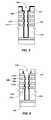
- One or more portions of the conductive structure 100may be formed as a so-called “stair step” structure including a plurality of steps 106 (e.g., steps 107 , 108 , 109 , 110 ), each step 107 , 108 , 109 , 110 being formed at least from a conductive material 112 (e.g., polysilicon).
- the conductive materials 112may form a stair step structure over the interconnect 103 and the substrate 104 .
- Each conductive step 107 , 108 , 109 , 110may be insulated from (e.g., electrically insulated, separated, or isolated from) one or more adjacent steps 106 by insulative material 114 (e.g., an electrically insulative material such as a dielectric material).
- one or more steps 106may be formed by more than one conductive material 112 where each of the conductive steps 106 are at least partially insulated from one another with one or more insulative materials 114 .
- the conductive material 112 of the step most proximal to the interconnect 103 and the substrate 104may be separated from the interconnect 103 by an insulative material 115 .
- insulative materialsmay also be disposed on a distal portion of each of the steps 106 .
- insulative materialse.g., insulative materials 114 , 115 , 117
- insulative materialsmay include any suitable at least partially electrically insulating materials such as an oxide material (e.g., SiO 2 , Al 2 O 3 , etc.), a nitride material (e.g., Si 3 N 4 , MN, etc.), or a combination of oxide and nitride materials such as, for example, an oxynitride material, a re-oxidized oxynitride material, or a so-called “oxide-nitride-oxide” (ONO) structure.
- the insulative material 114 , 115 , 117may each comprise similar materials, dissimilar materials, or combinations thereof.
- the conductive material 112 of each of the steps 106may form a conductive plate (e.g., a word line plate) for supplying electrical signals to a semiconductor device 102 ( FIG. 1 ) such as, for example, a plurality of memory cells.
- a conductive platee.g., a word line plate
- Each of the steps 106 of the stair step structuremay include a contact portion 105 to facilitate forming one or more connections (e.g., electrical connections) with each of the individual steps 106 as discussed in further detail below.
- each step 106may include a contact portion 105 that is laterally offset from one or more adjacent steps 106 .
- step 108includes a contact portion 105 (e.g., a lateral end portion of conductive material 112 ) extending laterally beyond an adjacent step (e.g., step 107 ). In other words, step 108 does not laterally extend the same distance as step 107 .
- an openingsuch as, for example, a contact hole 116 (e.g., a via) may extend through each of the steps 106 at the contact portion 105 of the steps 106 to enable each of the steps 106 to be individually contacted in order to provide a connection to each of the steps 106 .
- each of the steps 106may include a contact 118 formed in the contact hole 116 extending therethrough. The contact 118 may extend through the conductive materials 112 of each of the steps 106 .
- the contact 118may be formed from a conductive material such as, for example, a metal (e.g., W, Ni, tantalum nitride (TaN), Pt, tungsten nitride (WN), Au, titanium nitride (TiN), or titanium aluminum nitride (TiAlN)), polysilicon, or other conductive materials.
- a metale.g., W, Ni, tantalum nitride (TaN), Pt, tungsten nitride (WN), Au, titanium nitride (TiN), or titanium aluminum nitride (TiAlN)
- the contact 118may include one or more conductive materials foamed therein.
- the contact 118may include an outer portion formed from a different material (e.g., a liner 132 ( FIG.
- a distal portion 128 of the contact hole 116may be formed to have a lateral width (e.g., diameter) that is relatively greater than a width of a proximal portion 130 of the contact hole 116 .
- Such embodimentsmay enable the contact 118 to contact (and be in communication with) both a lateral side surface of the conductive material 112 of a step 106 (e.g., a surface extending along the contact hole 116 ) and a distal surface of the conductive material 112 of the step 106 .
- the contact 118may enable a respective one of the steps 106 to be in communication with the interconnect 103 (e.g., a conductive interconnect in communication with a CMOS device such a word line driver).
- the contact hole 116 and contact 118 formed thereinmay extend through a first step 107 and each step 108 , 109 , 110 underlying (e.g., positioned below in a direction extending toward the substrate 104 ). Stated in another way, the contact hole 116 and contact 118 formed therein may extend through one or more steps 106 in a direction extending from a distal portion of the conductive structure 100 to a proximal portion of the conductive structure 100 .
- the contact hole 116 and contact 118 formed thereinmay extend through step 107 and each step that step 107 is formed over (e.g., steps 108 , 109 , 110 ).
- the contact holes 116 and contacts 118may be positioned such that each contact hole 116 and contact 118 extends through a differing distal portion (e.g., contact portion 105 ) of the steps 106 forming the stair step structure.
- contact 119 formed in a contact hole 116may be positioned such that the contact 119 extends through a distal portion of step 107 (e.g., the conductive material 112 of step 107 ).
- Contact 120may be positioned to extend through a distal portion of step 108 (e.g., the conductive material 112 of step 108 ) while not extending through the distal portion of step 107 .
- each contact 118may be positioned such that the contact (e.g., contact 119 ) extends through a conductive material 112 of a step (e.g., step 107 ) that is positioned more distal from (i.e., a greater distance from) the interconnect 103 than a conductive material 112 of an adjacent step (e.g., step 108 ).
- one or more steps 106may be at least partially insulated from the contact 118 extending through the conductive steps 106 while one or more other conductive steps 106 may be in connection with the contact 118 .
- each step 108 , 109 , and 110 underlying step 107may be isolated from electrical communication with the contact 118 in the contact hole 116 by a liner 122 comprising an insulative material extending along a portion of the conductive structure forming the contact hole 116 , while step 107 is in contact with the contact 118 .
- the liner 122is formed between the contact 118 and the conductive materials 112 of steps 108 , 109 , and 110 , such that the conductive materials 112 of steps 108 , 109 , and 110 are insulated from the contact 118 .
- the liner 122is formed such that at least a portion of the contact 118 and the conductive material 112 of step 107 are in communication (e.g., in contact to enable electrical signals to pass between the contact 118 and the conductive material 112 of step 107 ).
- Each contact 118may be in electrical communication with a respective at least one of the steps 106 .
- contact 119may be in electrical communication with conductive step 107
- contact 120may be in electrical communication with conductive step 108 , etc.
- the liner 122may be formed from an insulative material such as those listed above.
- the conductive structure 100may have a stair step structure that enables the contacts 118 (e.g., contacts 119 , 120 , 121 ) to be formed as columns.
- the contacts 118may extend through a different number of steps 106 and be in communication with a selected (e.g., particular) one of the steps 106 .
- the contacts 118may each be in contact with the most distal of the steps 106 that the contact 118 extends through (e.g., the step 106 furthest from the interconnect 103 ). As shown in FIG.
- a contact 119may form a first column through the stair step structure of the conductive structure 100 and may be in communication with step 107 while being isolated from the steps 108 , 109 , and 110 by the liner 122 .
- a contact 120may form a second column through the stair step structure of the conductive structure 100 and may be in communication with step 108 while being isolated from steps 109 and 110 by the liner 122 , and so on. This or a similar pattern may continue in a similar manner until a contact 121 is in communication the most proximal of the steps 106 (e.g., step 110 ). It is noted that while the embodiment of FIG.
- conductive structures 100may be formed with any number of steps including any number of conductive materials and insulative materials. It is further noted that while the embodiment of FIG. 2 illustrates each of the steps 106 having one conductive material 112 separated by an insulative material 114 , in other embodiments, the steps 106 may include one or more conductive materials (e.g., one or more conductive materials, each separated by insulative material). It is also noted that while the embodiment of FIG. 2 illustrates a conductive material 112 formed over (e.g., on) insulative material 114 , in other embodiments, the order of the conductive material 112 and the insulative material 114 may be reversed. Further, in yet other embodiments, contacts extending through the steps may be in communication with or isolation from any number of conductive materials in each step or in the overall conductive structure.
- the liner 122may be formed to enable an interface between the conductive material 112 of the steps 106 and the contact 118 on a lateral surface (e.g., a side surface) of the conductive material 112 and a distal surface of the conductive material. Such a configuration may be utilized to enhance the connection between the conductive material 112 of the steps 106 and the contact 118 .
- the liner 122may be formed to insulate one or more of the conductive steps 106 while enabling communication with one or more of the remaining conductive steps 106 while also enabling communication with the interconnect 103 formed at a proximal end of the contacts 118 .
- elements of the conductive structure 100e.g., the contact holes 116 , the contacts 118 , the liner 122 , etc.
- contact holes and contactsare shown in the drawings as having contact holes and contacts as being positioned substantially in the same cross-sectional plane for convenience and clarity. It is contemplated that the contact holes and contacts may be formed in the same cross-sectional planes, differing cross-sectional planes, or combinations thereof.
- conductive structuressuch as the conductive structure shown in FIG. 2
- the methodsare described, in some instances, with reference to a portion of the conductive structures (e.g., illustrating one contact hole and a contact disposed therein extending through a portion of conductive materials that form, for example, a portion a stair step structure).
- a plurality of contact holes and contactsmay be formed substantially simultaneously in one or more conductive structures.
- the materials forming the conductive structuresmay be formed by, for example, growing, diffusing, depositing, or otherwise providing thereon.
- the various materialsmay be formed using, for example, deposition techniques (e.g., chemical vapor deposition (CVD), physical vapor deposition (PVD), atomic layer deposition (ALD), sputtering, thermal evaporation, or plating), oxidation processes (e.g., thermal oxidation, ISSG oxidation), and patterning techniques (e.g., masking and etching) known in the art of integrated circuit fabrication.
- the insulative materialsmay be formed by chemical vapor deposition, by decomposing tetraethyl orthosilicate (TEOS), or by any other process known in the art of integrated circuit fabrication.
- the materials or portions thereofmay be removed using, for example, an abrasion or polishing process (e.g., a chemical-mechanical planarization (CMP) process, a chemical polishing process, a mechanical planarization process), an etching process, a lift-off process, or a combination thereof.
- Etching processesmay include, for example, wet or dry etching such as removing portions of a material using a mask and an anisotropic etching process (e.g., a reactive ion etching process, such as using a plasma) or removing portions of a material using a mask and an isotropic process (e.g., a chemical etching process).
- abrasion or polishing processe.g., a chemical-mechanical planarization (CMP) process, a chemical polishing process, a mechanical planarization process
- Etching processesmay include, for example, wet or dry etching such as removing portions of a material using a mask and an anisotropic
- the conductive structure 100may be formed, for example, as a stair step structure by forming a plurality of steps 106 (e.g., steps 107 , 108 , 109 , 110 ) including conductive materials 112 at least partially separated by insulative materials 114 , removing a portion of the conductive materials 112 and insulative materials 114 to form the steps 106 , forming an insulative material (e.g., insulative material 117 ) over the steps 106 , and planarizing the structure, such as through an abrasion process.
- steps 106e.g., steps 107 , 108 , 109 , 110
- One or more contact holes 116may be formed (e.g., through an etching process such as an anisotropic etch) in a workpiece (e.g., stair step structure) extending through the insulative materials (e.g., insulative materials 114 , 115 , 117 ) and through one or more conductive steps 106 .
- the contact holes 116may extend substantially to the interconnect 103 .
- the contact holes 116may be positioned such that each contact hole 116 extends through a distal portion of each step 106 (e.g., the contact portion 105 ( FIG. 2 ).
- the contact holes 116extend from a distal portion of the conductive structure 100 (e.g., a surface of insulative material 117 ) to a proximal portion (e.g., the interconnect 103 ) of the conductive structure 100 .
- Each contact hole 116may be positioned to first extend through, in a direction from a distal portion to a proximal portion of the conductive structure 100 , a differing step 106 .
- a first contact hole 116e.g., contact hole 124
- a second contact hole 116first extends, in a direction from a distal portion to a proximal portion of the conductive structure 100 , through step 108 and so on.
- a distal portion 128 of the contact holes 116may be formed to have a width (e.g., diameter) greater than a width of a proximal portion 130 of the contact holes 116 .
- the insulative material 114 , 117may be etched to form the wider distal portion 128 of the contact holes 116 extending from the most distal conductive material 112 of each of the steps 106 to a distal end of the insulative material 117 .
- the wider distal portions 128 of the contact holes 116may be formed by etching (e.g., an isometric etch including an etchant with selectivity to the insulative materials 114 , 117 ).
- the chemistry of the etchantmay be configured to remove the insulative materials 114 , 117 at a faster rate as compared to the removal rate of other materials.
- FIGS. 5 through 11illustrate a single contact hole 116 and contact 118 of a portion of the workpiece shown in FIGS. 3 and 4 .
- one or more contact holesmay be processed in a similar manner either substantially simultaneously with the contact hole 116 shown in FIG. 5 or in separate processes.
- the etchinge.g., isometric etching
- the etching of the insulative material 114 , 115 , 117may also form recesses in the insulative material 114 extending between the steps 106 and in the insulative materials 115 , 117 . If present, the recesses may increase portions of the width of the contact hole 116 .
- forming the contact holes 116 in the insulative materials 114 , 115 , 117may not substantially form recesses in the insulative material 114 extending between the conductive steps 106 or in the insulative materials 115 , 117 such as the contact holes shown in FIGS. 12 through 16 .
- the liner 122may be formed in contact hole 116 .
- the liner 112may at least substantially cover the conductive material 112 of each of the steps 106 exposed in the contact hole 116 .
- the liner 122may be formed (e.g., conformally deposited) in the contact hole 116 such that a portion of the contact hole 116 remains unfilled.
- a portion of the liner 122may be removed to expose one or more of the conductive steps 106 .
- Another portion of the liner 122may be removed to expose the interconnect 103 .
- Portions of the liner 112may be removed using one or more etching processes such as, for example, one of more anisotropic etching processes.
- an etchant with selectivity to the insulative material forming the liner 122may be applied to the workpiece in an anisotropic etching process that removes horizontal surfaces (e.g., surfaces of the liner 122 extending in a lateral direction) faster than vertical surfaces (e.g., surfaces extending in a longitudinal direction).
- the same etching process or a different etching processmay also remove vertical portions of the liner 122 overlying the most distal of the steps 106 (e.g., step 107 ). As shown in FIG. 6 , such a process may expose the lateral and longitudinal surfaces of the conductive material 112 of the most distal of the steps 106 (e.g., step 107 ) while the conductive materials 112 of steps 108 , 109 , and 110 may remain substantially covered with the liner 122 .
- materials selected for the liner 122 and the insulative material 114 , 115 , 117may affect the structure of the liner 122 after portions of the liner 112 have been removed.
- the liner 122 and the insulative material 117are formed from the same material (e.g., an oxide), the distal portion of the liner 122 may not recess in the manner shown in FIG. 6 . Nonetheless, any suitable materials and removal process may be utilized to at least partially expose a portion of one or more selected conductive steps 106 in order to make a connection between the contact 118 and the one or more selected conductive steps 106 .
- a conductive liner 132may be formed in the contact hole 116 to enable communication between one or more selected conductive steps 106 , the interconnect 103 , and a contact 118 ( FIG. 8 ) that is formed in the contact hole 116 .
- the conductive liner 132(or processes utilized to prepare the workpiece for the conductive liner 132 ) may act to clean surfaces of the conductive materials 112 and the interconnect 103 in order to enable communication between the conductive materials 112 , the interconnect 103 , and the contact 118 ( FIG. 8 ).
- the conductive liner 132may comprise a conductive material and may be in communication with the conductive materials 112 and the interconnect 103 .
- the contact 118FIG. 8
- the contact 118may be in communication with the conductive materials 112 and the interconnect 103 via the conductive liner 132 .
- FIG. 8illustrates forming a conductive material in the contact hole 116 in accordance with an embodiment of the present disclosure.
- the conductive materialmay be conformally deposited. As shown in FIG. 8 , in some embodiments, the conductive material may substantially fill the contact hole 116 , forming the contact 118 . In some embodiments where the conductive material is conformally deposited, a distal portion 128 of the contact hole 116 may be sized to have a width (e.g., diameter) that enables the conductive material of the contact 118 to pinch-off within a proximal portion 130 of the contact hole 116 .
- a widthe.g., diameter
- the distal portion 128 of the contact hole 116may be sized to have a width that enables the substantial closing off of the contact hole 116 with the conductive material of the contact 118 at the proximal potion 130 of the contact hole 116 .
- the distal portion 128 of the contact hole 116may be sized to have a width sufficient to enable pinching-off of the contact 118 in the proximal portion 130 of the contact hole 116 but not in the distal portion 128 of the contact hole 116 .
- the width of the distal portion 128 of the contact hole 116 enabling the material to pinch-off thereinwill vary based at least partially on the material used to fill the contact hole 116 and the technique used to deposit the material.
- the conductive materialmay also extend over the insulative material 117 .
- the conductive material forming the contact 118may be deposited such that the contact 118 is in communication with one or more of the conductive steps 106 and the interconnect 103 . As discussed above, in some embodiments, both the conductive material deposited in the act shown in FIG. 8 and the liner 132 ( FIG. 7 ) may form the contact 118 .
- FIG. 9illustrates forming a conductive material in the contact hole 116 in accordance with another embodiment of the present disclosure.
- the conductive materialmay also extend over the insulative material 117 .
- a distal portion 128 of the contact hole 116may be sized to have a width (e.g., diameter) that enables conductive material deposited in the contact hole 116 to form the contact 118 to pinch-off within the distal portion 128 of the contact hole 116 .
- the distal portion 128 of the contact hole 116may be sized to have a width that enables the substantial closing off of the contact hole 116 with the conductive material of the contact 118 at the distal potion 128 of the contact hole 116 .
- the distal portion 128 of the contact hole 116may be sized to have a width sufficient to enable pinching-off of the contact 118 in the distal portion 128 of the contact hole 116 rather than a width where the conductive material of the contact 118 will at least partially not pinch-off in the distal portion 128 of the contact hole 116 (see, e.g., FIG. 8 ). It is noted that the width of the distal portion 128 of the contact hole 116 enabling the material to pinch-off therein will vary based at least partially on the material used to fill the contact hole 116 and the technique used to deposit the material.
- FIGS. 10 and 11illustrate partially removing material of the workpiece (e.g., the conductive material of the contact 118 overlying the insulative material 117 and portions of the conductive material in the contact hole 116 ) in accordance with embodiments of the present disclosure such as, for example, by etching as shown in FIG. 10 and by an abrasion process as shown in FIG. 11 .
- material of the contact 118may be removed using an etching process such as, for example, an isotropic dry etch.
- the material of the contact 118may be removed such that a portion of the contact 118 is in communication with one or more conductive steps 106 .
- the etching processmay remove the material of the contact 118 overlying the insulative material 117 and a portion of the material within the distal portion 128 .
- the material of the contact 118may be etched such that the contact 118 does not extend past a distal end of the insulative material 117 .
- the material of the contact 118may be at least partially recessed with the distal portion 128 of the contact hole 116 .
- material of the contact 118may be removed using an abrasion process such as, for example, a polishing process (e.g., a chemical-mechanical planarization (CMP) process).
- the material of the contact 118may be removed such that a portion of the contact 118 is in communication with one or more conductive steps 106 .
- the material of the contact 118may be etched such that the contact 118 does not extend past a distal end of the insulative material 117 .
- the material of the contact 118may be substantially planar with the distal portion 128 of the contact hole 116 (e.g., substantially planar with a distal end of the insulative material 117 ). It is noted that the embodiments described above with reference to FIGS. 10 and 11 may also include removing at least a portion of other materials of the workpiece such as, for example, a portion of the insulative material 117 .
- FIG. 12Another embodiment of a method that may be used to form, for example, the conductive structure 100 shown in FIG. 2 is described with reference to FIGS. 12 through 14 .
- one or more contact holes 116 similar to the contact holes 116 shown and described with reference to FIG. 3may be formed in the workpiece extending through the insulative materials (e.g., insulative materials 114 , 115 , 117 ) and through one or more conductive steps 106 .
- the contact holes 116may extend substantially to the interconnect 103 .
- the contact holes 116may be formed by forming a mask 134 (e.g., a hard mask (amorphous carbon or transparent carbon), a photoresist, etc.) on a distal end of the workpiece (e.g., the distal end of the insulative material 117 ) and etching (e.g., an anisotropic etch) a pattern of the mask 134 through the workpiece.
- a mask 134e.g., a hard mask (amorphous carbon or transparent carbon), a photoresist, etc.
- etchinge.g., an anisotropic etch
- one or more openings (e.g., apertures 136 ) in the mask 134may define a first width of each of the contact holes 116 (e.g., the width of the proximal portion 130 of the contact holes 116 ).
- a portion of the mask 134may be removed (e.g., trimmed) to increase the width of the apertures 136 of the mask 134 .
- the mask 134 including the relatively wider apertures 136 ′may be used to etch another portion of the workpiece.
- the insulative material 117may be etched (e.g., an anisotropic etch) to form a distal portion 128 of the contact holes 116 .
- the distal portion 128 of the contact holes 116may be formed to have a width (e.g., diameter) greater than a width of a proximal portion 130 of the contact holes 116 .
- the relatively wider distal portion 128 of the contact hole 116may extend from a distal end of the workpiece (e.g., a distal end of the insulative material 117 ) to the distal surface of the conductive step 106 (e.g., the conductive material 112 of the most distal of the steps 106 ).
- the workpiecemay be formed into a conductive structure (e.g., conductive structure 100 as shown in FIG. 2 ) by forming a liner and contacts in the contact holes through processes such as, for example, those described above with reference to FIGS. 5 through 11 .
- the mask 134may also be removed from the workpiece.
- the mask 134may be removed through an etching or abrasion process such as those described above with reference to FIGS. 11 and 12 (e.g., concurrently with the removal of the material of the contact 118 ).
- one or more contact holes 116 similar to the contact holes 116 shown and described with reference to FIG. 3may be formed in the workpiece extending through the insulative materials (e.g., insulative materials 114 , 115 , 117 ) and through one or more conductive steps 106 .
- the contact holes 116may extend substantially to the interconnect 103 .
- a mask 134e.g., a hard mask, a photoresist, etc.
- one or more apertures 136 in the mask 134may define a first width of each of the contact holes 116 (e.g., the width of a distal portion 128 of the contact hole 116 ).
- the apertures 136 formed by the mask 134may be used to etch (e.g., an anisotropic etch) the insulative material 117 to form a portion of the contact holes 118 (e.g., a distal portion 128 of the contact holes 118 ).
- the distal portion 128 of the contact hole 116may extend from a distal end of the workpiece (e.g., a distal end of the insulative material 117 ) to a conductive step 106 (e.g., the conductive material 112 of the most distal of the steps 106 ).
- a spacer 138may be formed on vertical sidewalls of the mask 134 and the insulative material 117 , at least partially within the distal portion 132 of the contact hole 116 .
- the spacer 138may reduce (e.g., narrow) the first width of the apertures 136 ′.
- the spacer 138may be formed from a material that is selectively etchable relative to the conductive material 112 and the insulative material 114 .
- the spacer 138may be used to define a width of each of the contact holes 116 (e.g., the width of a proximal portion 130 of the contact holes 116 ).
- An etching process(e.g., anisotropic etch with selectivity to the conductive material 112 and insulative materials 114 , 115 ) through the relative narrower apertures 136 ′ may be used to form the remaining portion of the contact holes 116 (e.g., proximal portion 130 of the contact holes 116 ) at a width less than the width of the distal portion 128 of the contact hole 116 .
- the spacer 138 and the mask 134 formed on the distal end of insulative material 117may be removed (e.g., through an etching process, an abrasion process, or combination thereof).
- the workpiecemay be formed into a conductive structure (e.g., conductive structure 100 as shown in FIG. 2 ) by depositing a liner and contacts in the contact holes through processes such as, for example, those described above with reference to FIGS. 5 through 11 .
- a conductive structuree.g., conductive structure 100 as shown in FIG. 2
- Embodiments of the present disclosuremay be particularly useful in forming conductive structures (e.g., a stair step structure) that enable communication with one or more semiconductor devices (e.g., a CMOS device such a word line driver, memory cells, etc.) utilizing contacts extending at least partially through the conductive structure.
- conductive structurese.g., a stair step structure
- semiconductor devicese.g., a CMOS device such a word line driver, memory cells, etc.
- Such configurationsmay enable a relatively more direct route of connection through the conductive structure as compared to conventional conductive structures in which contacts extend up from and over the stair step conductive structure.
- Such a configuration with contacts extending through the conductive structuremay reduce the need for forming tight pitch wiring above the stair step conductive structure by enabling a relatively simplified and shortened route of connection to conductive elements positioned beneath the conductive structure.
- a conductive structurein an embodiment, includes a plurality of conductive steps extending laterally along the conductive structure where each conductive step of the plurality of conductive steps is at least partially separated from an adjacent conductive step of the plurality of conductive steps by insulative material.
- the conductive structurefurther includes a contact extending at least partially through at least two conductive steps of the plurality of conductive steps, wherein the contact is in communication with at least one of the conductive steps and insulated from at least another one of the conductive steps.
- a devicein a further embodiment, includes a plurality of memory cells and a conductive structure.
- the conductive structureincludes a plurality of conductive steps where each conductive step of the plurality of conductive steps is in electrical communication with a respective at least one memory cell of the plurality of memory cells.
- the conductive structurefurther includes a plurality of contacts each extending through at least one conductive step of the plurality of conductive steps, each contact of the plurality of contacts being in electrical communication with a respective at least one of the plurality of conductive steps and being insulated from another conductive step of the plurality of conductive steps with insulative material at least partially between the contact and the another conductive step.
- a systemin electrical communication with the semiconductor device.
- the conductive structureincludes a stair step structure comprising a plurality of steps each having a lateral end portion laterally offset from a lateral end portion of an adjacent step. Each step comprising conductive material and insulative material at least partially separating a respective step of the plurality of steps from an adjacent step of the plurality of steps.
- the conductive structurefurther includes a plurality of contacts, each contact of the plurality of contacts extending through at least one step of the plurality of steps and being in communication with at least one respective step of the plurality of steps.
- a method of forming a conductive structureincludes forming a plurality of openings through at least one of a plurality of conductive materials, each conductive material being at least partially separated by a respective insulative material of a plurality of insulative materials, forming a liner in each opening of the plurality of openings, exposing a portion of a respective at least one conductive material of the plurality of conductive materials in each opening of the plurality of openings, and foaming a respective contact in each opening of the plurality of openings in communication with the exposed portion of the respective at least one conductive material of the plurality of conductive materials.
- a method of forming electrical connections for a stair step conductive structureincludes forming a plurality of steps each having a lateral end portion laterally offset from a lateral end portion of an adjacent step over an interconnect, forming an opening through each step of the plurality of steps extending through the plurality of steps to the interconnect, and forming a contact in the opening in electrical communication with at least one of the plurality of steps and the interconnect.
Landscapes
- Engineering & Computer Science (AREA)
- Physics & Mathematics (AREA)
- Condensed Matter Physics & Semiconductors (AREA)
- General Physics & Mathematics (AREA)
- Computer Hardware Design (AREA)
- Microelectronics & Electronic Packaging (AREA)
- Power Engineering (AREA)
- Manufacturing & Machinery (AREA)
- Internal Circuitry In Semiconductor Integrated Circuit Devices (AREA)
Abstract
Description
Claims (27)
Priority Applications (10)
| Application Number | Priority Date | Filing Date | Title |
|---|---|---|---|
| US13/151,945US8765598B2 (en) | 2011-06-02 | 2011-06-02 | Conductive structures, systems and devices including conductive structures and related methods |
| CN201610935237.8ACN106847789B (en) | 2011-06-02 | 2012-05-23 | Conductive structures, systems and devices incorporating conductive structures, and related methods |
| PCT/US2012/039042WO2012166451A2 (en) | 2011-06-02 | 2012-05-23 | Conductive structures, systems and devices including conductive structures and related methods |
| CN201280026880.9ACN103582944B (en) | 2011-06-02 | 2012-05-23 | Conductive structures, systems and devices incorporating conductive structures, and related methods |
| KR1020137030533AKR101533521B1 (en) | 2011-06-02 | 2012-05-23 | Conductive structures, systems and devices including conductive structures and related methods |
| TW101119863ATWI492333B (en) | 2011-06-02 | 2012-06-01 | Conductive structure, system and apparatus including conductive structure, and related methods |
| US14/308,339US9536823B2 (en) | 2011-06-02 | 2014-06-18 | Conductive structures, systems and devices including conductive structures and related methods |
| US15/393,553US9911692B2 (en) | 2011-06-02 | 2016-12-29 | Conductive structures, systems and devices including conductive structures and related methods |
| US15/885,086US10290575B2 (en) | 2011-06-02 | 2018-01-31 | Memory devices, semiconductor devices and related methods |
| US16/409,464US10930585B2 (en) | 2011-06-02 | 2019-05-10 | Memory devices, semiconductor devices and related methods |
Applications Claiming Priority (1)
| Application Number | Priority Date | Filing Date | Title |
|---|---|---|---|
| US13/151,945US8765598B2 (en) | 2011-06-02 | 2011-06-02 | Conductive structures, systems and devices including conductive structures and related methods |
Related Child Applications (1)
| Application Number | Title | Priority Date | Filing Date |
|---|---|---|---|
| US14/308,339ContinuationUS9536823B2 (en) | 2011-06-02 | 2014-06-18 | Conductive structures, systems and devices including conductive structures and related methods |
Publications (2)
| Publication Number | Publication Date |
|---|---|
| US20120306090A1 US20120306090A1 (en) | 2012-12-06 |
| US8765598B2true US8765598B2 (en) | 2014-07-01 |
Family
ID=47260189
Family Applications (5)
| Application Number | Title | Priority Date | Filing Date |
|---|---|---|---|
| US13/151,945Active2031-11-09US8765598B2 (en) | 2011-06-02 | 2011-06-02 | Conductive structures, systems and devices including conductive structures and related methods |
| US14/308,339Active2031-06-20US9536823B2 (en) | 2011-06-02 | 2014-06-18 | Conductive structures, systems and devices including conductive structures and related methods |
| US15/393,553ActiveUS9911692B2 (en) | 2011-06-02 | 2016-12-29 | Conductive structures, systems and devices including conductive structures and related methods |
| US15/885,086ActiveUS10290575B2 (en) | 2011-06-02 | 2018-01-31 | Memory devices, semiconductor devices and related methods |
| US16/409,464ActiveUS10930585B2 (en) | 2011-06-02 | 2019-05-10 | Memory devices, semiconductor devices and related methods |
Family Applications After (4)
| Application Number | Title | Priority Date | Filing Date |
|---|---|---|---|
| US14/308,339Active2031-06-20US9536823B2 (en) | 2011-06-02 | 2014-06-18 | Conductive structures, systems and devices including conductive structures and related methods |
| US15/393,553ActiveUS9911692B2 (en) | 2011-06-02 | 2016-12-29 | Conductive structures, systems and devices including conductive structures and related methods |
| US15/885,086ActiveUS10290575B2 (en) | 2011-06-02 | 2018-01-31 | Memory devices, semiconductor devices and related methods |
| US16/409,464ActiveUS10930585B2 (en) | 2011-06-02 | 2019-05-10 | Memory devices, semiconductor devices and related methods |
Country Status (5)
| Country | Link |
|---|---|
| US (5) | US8765598B2 (en) |
| KR (1) | KR101533521B1 (en) |
| CN (2) | CN106847789B (en) |
| TW (1) | TWI492333B (en) |
| WO (1) | WO2012166451A2 (en) |
Cited By (22)
| Publication number | Priority date | Publication date | Assignee | Title |
|---|---|---|---|---|
| US20130307160A1 (en)* | 2012-05-21 | 2013-11-21 | International Business Machines Corporation | Via Structure For Three-Dimensional Circuit Integration |
| US20160056206A1 (en)* | 2014-08-25 | 2016-02-25 | HGST, Inc. | 3-d planes memory device |
| US9466531B2 (en) | 2011-06-02 | 2016-10-11 | Micron Technology, Inc. | Apparatuses including stair-step structures and methods of forming the same |
| US9570392B2 (en)* | 2015-04-30 | 2017-02-14 | Kabushiki Kaisha Toshiba | Memory device and method for manufacturing the same |
| US9716104B2 (en) | 2015-08-07 | 2017-07-25 | Samsung Electronics Co., Ltd. | Vertical memory devices having dummy channel regions |
| US9991271B2 (en) | 2016-06-09 | 2018-06-05 | Samsung Electronics Co., Ltd. | Integrated circuit device including vertical memory device and method of manufacturing the same |
| US10141330B1 (en) | 2017-05-26 | 2018-11-27 | Micron Technology, Inc. | Methods of forming semiconductor device structures, and related semiconductor device structures, semiconductor devices, and electronic systems |
| US10269625B1 (en) | 2017-12-28 | 2019-04-23 | Micron Technology, Inc. | Methods of forming semiconductor structures having stair step structures |
| US10381362B1 (en)* | 2018-05-15 | 2019-08-13 | Sandisk Technologies Llc | Three-dimensional memory device including inverted memory stack structures and methods of making the same |
| US10685975B2 (en) | 2018-09-13 | 2020-06-16 | Samsung Electronics Co., Ltd. | Vertical memory device and method of fabrication the same |
| US10748923B2 (en) | 2018-04-20 | 2020-08-18 | Samsung Electronics Co., Ltd. | Vertical memory devices and methods of manufacturing the same |
| US10978475B2 (en) | 2018-12-14 | 2021-04-13 | Samsung Electronics Co., Ltd. | Three-dimensional semiconductor memory device |
| US11049768B2 (en) | 2019-10-29 | 2021-06-29 | Micron Technology, Inc. | Methods of forming microelectronic devices, and related microelectronic devices, and electronic systems |
| US11164886B2 (en) | 2019-05-15 | 2021-11-02 | Samsung Electronics Co., Ltd. | Three-dimensional semiconductor memory device |
| US11251192B2 (en) | 2018-06-11 | 2022-02-15 | Samsung Electronics Co., Ltd. | Semiconductor devices and manufacturing methods of the same |
| US11437318B2 (en) | 2020-06-12 | 2022-09-06 | Micron Technology, Inc. | Microelectronic devices including staircase structures, and related memory devices and electronic systems |
| US11495540B2 (en)* | 2019-10-22 | 2022-11-08 | Tokyo Electron Limited | Semiconductor apparatus having stacked devices and method of manufacture thereof |
| US11824041B2 (en) | 2016-12-29 | 2023-11-21 | Intel Corporation | Hyperchip |
| EP4373235A1 (en)* | 2022-11-18 | 2024-05-22 | Samsung Electronics Co., Ltd. | Semiconductor device and electronic system including the semiconductor device |
| US12075624B2 (en) | 2020-11-17 | 2024-08-27 | Samsung Electronics Co., Ltd. | Three-dimensional semiconductor memory device |
| US12347778B2 (en) | 2021-08-13 | 2025-07-01 | Samsung Electronics Co., Ltd. | Semiconductor device and electronic system including the same |
| US12355003B2 (en) | 2021-04-16 | 2025-07-08 | Samsung Electronics Co., Ltd. | Semiconductor devices and data storage systems including the same |
Families Citing this family (69)
| Publication number | Priority date | Publication date | Assignee | Title |
|---|---|---|---|---|
| US8765598B2 (en) | 2011-06-02 | 2014-07-01 | Micron Technology, Inc. | Conductive structures, systems and devices including conductive structures and related methods |
| US9595533B2 (en) | 2012-08-30 | 2017-03-14 | Micron Technology, Inc. | Memory array having connections going through control gates |
| US20150187701A1 (en) | 2013-03-12 | 2015-07-02 | Taiwan Semiconductor Manufacturing Company, Ltd. | Semiconductor Devices and Methods of Manufacture Thereof |
| US10056353B2 (en) | 2013-12-19 | 2018-08-21 | Taiwan Semiconductor Manufacturing Company, Ltd. | 3DIC interconnect apparatus and method |
| US9412719B2 (en) | 2013-12-19 | 2016-08-09 | Taiwan Semiconductor Manufacturing Company, Ltd. | 3DIC interconnect apparatus and method |
| KR20150073251A (en)* | 2013-12-20 | 2015-07-01 | 에스케이하이닉스 주식회사 | Semiconductor device and method of manufacturing the same |
| US9601348B2 (en)* | 2014-03-13 | 2017-03-21 | Taiwan Semiconductor Manufacturing Company, Ltd. | Interconnect structure and method of forming same |
| US9455158B2 (en) | 2014-05-30 | 2016-09-27 | Taiwan Semiconductor Manufacturing Company, Ltd. | 3DIC interconnect devices and methods of forming same |
| US9449914B2 (en) | 2014-07-17 | 2016-09-20 | Taiwan Semiconductor Manufacturing Company, Ltd. | Stacked integrated circuits with redistribution lines |
| KR20160013756A (en) | 2014-07-28 | 2016-02-05 | 에스케이하이닉스 주식회사 | Interconnection structure, semiconductor device and manufaturing method thereof |
| TWI571907B (en)* | 2015-06-18 | 2017-02-21 | 旺宏電子股份有限公司 | Opening structure and manufacturing method thereof and interconnect structure |
| US10541204B2 (en)* | 2015-10-20 | 2020-01-21 | Taiwan Semiconductor Manufacturing Co., Ltd. | Interconnection structure and method of forming the same |
| US9941209B2 (en) | 2016-03-11 | 2018-04-10 | Micron Technology, Inc. | Conductive structures, systems and devices including conductive structures and related methods |
| US10283520B2 (en) | 2016-07-12 | 2019-05-07 | Micron Technology, Inc. | Elevationally-extending string of memory cells individually comprising a programmable charge storage transistor and method of forming an elevationally-extending string of memory cells individually comprising a programmable charge storage transistor |
| US10090318B2 (en) | 2016-08-05 | 2018-10-02 | Micron Technology, Inc. | Vertical string of memory cells individually comprising a programmable charge storage transistor comprising a control gate and a charge storage structure and method of forming a vertical string of memory cells individually comprising a programmable charge storage transistor comprising a control gate and a charge storage structure |
| KR102679478B1 (en)* | 2016-12-09 | 2024-07-01 | 삼성전자주식회사 | Semiconductor memory device |
| US10707121B2 (en) | 2016-12-31 | 2020-07-07 | Intel Corporatino | Solid state memory device, and manufacturing method thereof |
| US20180197874A1 (en)* | 2017-01-11 | 2018-07-12 | Toshiba Memory Corporation | Semiconductor device and method for manufacturing same |
| US10192929B2 (en)* | 2017-03-24 | 2019-01-29 | Sandisk Technologies Llc | Three-dimensional memory devices having through-stack contact via structures and method of making thereof |
| KR20180110797A (en)* | 2017-03-30 | 2018-10-11 | 에스케이하이닉스 주식회사 | Semiconductor device and manufacturing method thereof |
| US10923492B2 (en) | 2017-04-24 | 2021-02-16 | Micron Technology, Inc. | Elevationally-extending string of memory cells and methods of forming an elevationally-extending string of memory cells |
| US10373904B2 (en)* | 2017-08-28 | 2019-08-06 | Micron Technology, Inc. | Semiconductor devices including capacitors, related electronic systems, and related methods |
| US11177271B2 (en)* | 2017-09-14 | 2021-11-16 | Micron Technology, Inc. | Device, a method used in forming a circuit structure, a method used in forming an array of elevationally-extending transistors and a circuit structure adjacent thereto |
| CN107994024B (en)* | 2017-11-23 | 2020-05-12 | 长江存储科技有限责任公司 | Preparation method of 3D NAND wire hole including silicon-rich silicon nitride isolation dielectric layer |
| EP3732704A4 (en) | 2017-12-27 | 2021-07-28 | INTEL Corporation | INTEGRATED CIRCUITS WITH LINE INTERRUPTIONS AND LINE BRIDGES WITHIN A SINGLE CONNECTION LEVEL |
| DE112017008330T5 (en) | 2017-12-27 | 2020-09-03 | Intel Corporation | INTEGRATED CIRCUITS (ICS) WITH ELECTROMIGRATION (EM) RESISTANT SEGMENTS IN ONE CONNECTING LEVEL |
| WO2019132897A1 (en)* | 2017-12-27 | 2019-07-04 | Intel Corporation | Multiple layer metal-insulator-metal (mim) structure |
| US10971393B2 (en) | 2017-12-27 | 2021-04-06 | Intel Corporation | Metal-insulator-metal (MIM) structure supporting high voltage applications and low voltage applications |
| US10727248B2 (en)* | 2018-02-15 | 2020-07-28 | Sandisk Technologies Llc | Three-dimensional memory device containing through-memory-level contact via structures |
| US10971507B2 (en)* | 2018-02-15 | 2021-04-06 | Sandisk Technologies Llc | Three-dimensional memory device containing through-memory-level contact via structures |
| US10903230B2 (en) | 2018-02-15 | 2021-01-26 | Sandisk Technologies Llc | Three-dimensional memory device containing through-memory-level contact via structures and method of making the same |
| US10892267B2 (en) | 2018-02-15 | 2021-01-12 | Sandisk Technologies Llc | Three-dimensional memory device containing through-memory-level contact via structures and method of making the same |
| US10490569B2 (en)* | 2018-03-08 | 2019-11-26 | Sandisk Technologies Llc | Three-dimensional memory device and method of making the same using concurrent formation of memory openings and contact openings |
| JP2019161094A (en)* | 2018-03-15 | 2019-09-19 | 東芝メモリ株式会社 | Semi-conductor memory |
| JP2019161080A (en) | 2018-03-15 | 2019-09-19 | 東芝メモリ株式会社 | Semiconductor memory device |
| EP3667712A1 (en)* | 2018-12-12 | 2020-06-17 | IMEC vzw | Improved routing contacts for 3d memory |
| CN109716521A (en) | 2018-12-12 | 2019-05-03 | 长江存储科技有限责任公司 | Contact structures for three-dimensional storage part |
| CN109863587B (en) | 2019-01-25 | 2021-04-27 | 长江存储科技有限责任公司 | Method of forming a hole structure in a semiconductor device |
| CN109923668A (en)* | 2019-01-30 | 2019-06-21 | 长江存储科技有限责任公司 | Use the hybrid bonded of illusory bonding contacts |
| KR102618755B1 (en) | 2019-01-30 | 2023-12-27 | 양쯔 메모리 테크놀로지스 씨오., 엘티디. | Hybrid bonding using dummy bonded contacts and dummy interconnects |
| WO2020188775A1 (en) | 2019-03-19 | 2020-09-24 | キオクシア株式会社 | Semiconductor storage device |
| CN110112133A (en)* | 2019-03-29 | 2019-08-09 | 长江存储科技有限责任公司 | Three-dimensional storage part and preparation method thereof |
| KR102793136B1 (en)* | 2019-05-03 | 2025-04-10 | 삼성전자주식회사 | Semiconductor device |
| US11251200B2 (en)* | 2019-05-23 | 2022-02-15 | Tokyo Electron Limited | Coaxial contacts for 3D logic and memory |
| KR102812029B1 (en)* | 2019-06-20 | 2025-05-26 | 삼성전자주식회사 | Semiconductor devices |
| US11600519B2 (en)* | 2019-09-16 | 2023-03-07 | International Business Machines Corporation | Skip-via proximity interconnect |
| KR102740535B1 (en)* | 2019-10-22 | 2024-12-09 | 삼성전자주식회사 | Vertical memory devices |
| KR102735208B1 (en)* | 2019-12-19 | 2024-11-27 | 삼성전자주식회사 | Vertical memory devices |
| WO2021142747A1 (en)* | 2020-01-17 | 2021-07-22 | Yangtze Memory Technologies Co., Ltd. | Dual deck three-dimensional nand memory and method for forming the same |
| US11374000B2 (en) | 2020-03-10 | 2022-06-28 | Taiwan Semiconductor Manufacturing Company, Ltd. | Trench capacitor with lateral protrusion structure |
| JP2021150413A (en)* | 2020-03-18 | 2021-09-27 | キオクシア株式会社 | Semiconductor storage device and method for manufacturing semiconductor storage device |
| US11839166B2 (en)* | 2020-04-06 | 2023-12-05 | Globalfoundries Singapore Pte. Ltd. | RRAM devices and methods of forming RRAM devices |
| US11152284B1 (en)* | 2020-05-07 | 2021-10-19 | Sandisk Technologies Llc | Three-dimensional memory device with a dielectric isolation spacer and methods of forming the same |
| US11264275B2 (en)* | 2020-05-12 | 2022-03-01 | Micron Technology, Inc. | Integrated assemblies and methods of forming integrated assemblies |
| CN111540752B (en)* | 2020-05-14 | 2021-05-18 | 长江存储科技有限责任公司 | 3D NAND memory and method of forming the same |
| KR102769746B1 (en)* | 2020-05-25 | 2025-02-17 | 에스케이하이닉스 주식회사 | Three dimensional memory device and method for fabricating threrof |
| KR102771196B1 (en) | 2020-06-03 | 2025-02-24 | 삼성전자주식회사 | Vertical memory devices |
| KR20220076804A (en)* | 2020-12-01 | 2022-06-08 | 삼성전자주식회사 | Semiconductor devices and data storage systems including the same |
| KR20220099039A (en) | 2021-01-05 | 2022-07-12 | 삼성전자주식회사 | Three-dimensional semiconductor memory device, manufacturing method of the same and electronic system including the same |
| KR102847561B1 (en) | 2021-02-09 | 2025-08-19 | 삼성전자주식회사 | Semiconductor device and electronic system including the same |
| US11735624B2 (en) | 2021-03-05 | 2023-08-22 | Taiwan Semiconductor Manufacturing Company, Ltd. | Multi-lateral recessed MIM structure |
| JP7706903B2 (en) | 2021-03-19 | 2025-07-14 | キオクシア株式会社 | Memory System |
| KR20220166892A (en) | 2021-06-10 | 2022-12-20 | 삼성전자주식회사 | Semiconductor devices and data storage systems including the same |
| KR20230025602A (en) | 2021-08-13 | 2023-02-22 | 삼성전자주식회사 | Semiconductor devices and data storage systems including the same |
| US12191249B2 (en)* | 2021-09-03 | 2025-01-07 | Micron Technology, Inc. | Microelectronic devices including staircase structures, and related memory devices, electronic systems, and methods |
| WO2023220968A1 (en)* | 2022-05-18 | 2023-11-23 | 华为技术有限公司 | Chip and preparation method therefor, and electronic device |
| WO2024036141A1 (en)* | 2022-08-08 | 2024-02-15 | Applied Materials, Inc. | Wordline sidewall contacts in 3d nand structures |
| CN118175848A (en)* | 2022-12-09 | 2024-06-11 | 长江存储科技有限责任公司 | Semiconductor device, preparation method and storage system |
| US20240213145A1 (en)* | 2022-12-21 | 2024-06-27 | Sandisk Technologies Llc | Three-dimensional memory device containing integrated contact-and-support assemblies and methods of making the same |
Citations (23)
| Publication number | Priority date | Publication date | Assignee | Title |
|---|---|---|---|---|
| JPS59182570A (en) | 1983-03-31 | 1984-10-17 | Fujitsu Ltd | semiconductor equipment |
| US5707885A (en) | 1995-05-26 | 1998-01-13 | Samsung Electronics Co., Ltd. | Method for manufacturing a vertical transistor having a storage node vertical transistor |
| US6858906B2 (en) | 2001-06-28 | 2005-02-22 | Samsung Electronics Co., Ltd. | Floating trap non-volatile semiconductor memory devices including high dielectric constant blocking insulating layers |
| US20060180851A1 (en) | 2001-06-28 | 2006-08-17 | Samsung Electronics Co., Ltd. | Non-volatile memory devices and methods of operating the same |
| US7253467B2 (en) | 2001-06-28 | 2007-08-07 | Samsung Electronics Co., Ltd. | Non-volatile semiconductor memory devices |
| US20070252201A1 (en) | 2006-03-27 | 2007-11-01 | Masaru Kito | Nonvolatile semiconductor memory device and manufacturing method thereof |
| US7315474B2 (en) | 2005-01-03 | 2008-01-01 | Macronix International Co., Ltd | Non-volatile memory cells, memory arrays including the same and methods of operating cells and arrays |
| US7361554B2 (en) | 2004-11-10 | 2008-04-22 | Samsung Electronics Co., Ltd. | Multi-bit non-volatile memory device, method of operating the same, and method of manufacturing the multi-bit non-volatile memory device |
| US20090020744A1 (en)* | 2007-06-29 | 2009-01-22 | Kabushiki Kaisha Toshiba | Stacked multilayer structure and manufacturing method thereof |
| US20090212350A1 (en) | 2008-02-25 | 2009-08-27 | Kabushiki Kaisha Toshiba | Nonvolatile semiconductor storage device and method of manufacturing the same |
| US20090310415A1 (en) | 2008-06-11 | 2009-12-17 | Jin Beom-Jun | Non-volatile memory devices including vertical nand strings and methods of forming the same |
| US20100090188A1 (en) | 2008-10-15 | 2010-04-15 | Takuya Futatsuyama | Semiconductor device |
| US7701771B2 (en) | 2006-08-04 | 2010-04-20 | Samsung Electronics Co., Ltd. | Memory device including 3-dimensionally arranged memory cell transistors and methods of operating the same |
| US20100133599A1 (en) | 2008-12-03 | 2010-06-03 | Samsung Electronics Co., Ltd. | Nonvolatile memory device and method for fabricating the same |
| US7776683B2 (en) | 2005-03-28 | 2010-08-17 | Micron Technology, Inc. | Integrated circuit fabrication |
| US20100224962A1 (en)* | 2009-03-03 | 2010-09-09 | Samsung Electronics Co., Ltd. | Integrated circuit resistive devices including multiple interconnected resistance layers |
| US20100230724A1 (en) | 2009-03-11 | 2010-09-16 | Micron Technology, Inc. | Methods for forming three-dimensional memory devices, and related structures |
| US7875985B2 (en) | 2006-12-22 | 2011-01-25 | Qimonda Ag | Memory device |
| US20110018036A1 (en) | 2009-07-22 | 2011-01-27 | Samsung Electronics Co., Ltd. | Vertical non-volatile memory device and method of fabricating the same |
| US20110031630A1 (en)* | 2009-08-04 | 2011-02-10 | Junichi Hashimoto | Semiconductor device manufacturing method and semiconductor device |
| JP2011060958A (en) | 2009-09-09 | 2011-03-24 | Toshiba Corp | Semiconductor device, and method of manufacturing the same |
| US20120261722A1 (en)* | 2011-04-12 | 2012-10-18 | Tang Sanh D | Stack Of Horizontally Extending And Vertically Overlapping Features, Methods Of Forming Circuitry Components, And Methods Of Forming An Array Of Memory Cells |
| US20120306089A1 (en) | 2011-06-02 | 2012-12-06 | Micron Technology, Inc. | Apparatuses including stair-step structures and methods of forming the same |
Family Cites Families (12)
| Publication number | Priority date | Publication date | Assignee | Title |
|---|---|---|---|---|
| NO20001360D0 (en)* | 2000-03-15 | 2000-03-15 | Thin Film Electronics Asa | Vertical electrical connections in stack |
| TW479294B (en)* | 2000-07-20 | 2002-03-11 | Vanguard Int Semiconduct Corp | Manufacturing method of shallow trench isolation structure |
| US6933224B2 (en)* | 2003-03-28 | 2005-08-23 | Micron Technology, Inc. | Method of fabricating integrated circuitry |
| JP2008277543A (en)* | 2007-04-27 | 2008-11-13 | Toshiba Corp | Nonvolatile semiconductor memory device |
| US20090277670A1 (en)* | 2008-05-10 | 2009-11-12 | Booth Jr Roger A | High Density Printed Circuit Board Interconnect and Method of Assembly |
| JP4956598B2 (en)* | 2009-02-27 | 2012-06-20 | シャープ株式会社 | Nonvolatile semiconductor memory device and manufacturing method thereof |
| US8383512B2 (en)* | 2011-01-19 | 2013-02-26 | Macronix International Co., Ltd. | Method for making multilayer connection structure |
| KR101602451B1 (en)* | 2010-01-22 | 2016-03-16 | 삼성전자주식회사 | Method of forming semiconductor device having contact plug and related device |
| US8765598B2 (en) | 2011-06-02 | 2014-07-01 | Micron Technology, Inc. | Conductive structures, systems and devices including conductive structures and related methods |
| US9478561B2 (en)* | 2015-01-30 | 2016-10-25 | Samsung Electronics Co., Ltd. | Semiconductor memory device and method of fabricating the same |
| US9818753B2 (en)* | 2015-10-20 | 2017-11-14 | Toshiba Memory Corporation | Semiconductor memory device and method for manufacturing the same |
| US9768233B1 (en)* | 2016-03-01 | 2017-09-19 | Toshiba Memory Corporation | Semiconductor device and method of manufacturing the same |
- 2011
- 2011-06-02USUS13/151,945patent/US8765598B2/enactiveActive
- 2012
- 2012-05-23KRKR1020137030533Apatent/KR101533521B1/enactiveActive
- 2012-05-23CNCN201610935237.8Apatent/CN106847789B/enactiveActive
- 2012-05-23CNCN201280026880.9Apatent/CN103582944B/enactiveActive
- 2012-05-23WOPCT/US2012/039042patent/WO2012166451A2/enactiveApplication Filing
- 2012-06-01TWTW101119863Apatent/TWI492333B/enactive
- 2014
- 2014-06-18USUS14/308,339patent/US9536823B2/enactiveActive
- 2016
- 2016-12-29USUS15/393,553patent/US9911692B2/enactiveActive
- 2018
- 2018-01-31USUS15/885,086patent/US10290575B2/enactiveActive
- 2019
- 2019-05-10USUS16/409,464patent/US10930585B2/enactiveActive
Patent Citations (24)
| Publication number | Priority date | Publication date | Assignee | Title |
|---|---|---|---|---|
| JPS59182570A (en) | 1983-03-31 | 1984-10-17 | Fujitsu Ltd | semiconductor equipment |
| US5707885A (en) | 1995-05-26 | 1998-01-13 | Samsung Electronics Co., Ltd. | Method for manufacturing a vertical transistor having a storage node vertical transistor |
| US6858906B2 (en) | 2001-06-28 | 2005-02-22 | Samsung Electronics Co., Ltd. | Floating trap non-volatile semiconductor memory devices including high dielectric constant blocking insulating layers |
| US20060180851A1 (en) | 2001-06-28 | 2006-08-17 | Samsung Electronics Co., Ltd. | Non-volatile memory devices and methods of operating the same |
| US7253467B2 (en) | 2001-06-28 | 2007-08-07 | Samsung Electronics Co., Ltd. | Non-volatile semiconductor memory devices |
| US7361554B2 (en) | 2004-11-10 | 2008-04-22 | Samsung Electronics Co., Ltd. | Multi-bit non-volatile memory device, method of operating the same, and method of manufacturing the multi-bit non-volatile memory device |
| US7315474B2 (en) | 2005-01-03 | 2008-01-01 | Macronix International Co., Ltd | Non-volatile memory cells, memory arrays including the same and methods of operating cells and arrays |
| US7776683B2 (en) | 2005-03-28 | 2010-08-17 | Micron Technology, Inc. | Integrated circuit fabrication |
| US20070252201A1 (en) | 2006-03-27 | 2007-11-01 | Masaru Kito | Nonvolatile semiconductor memory device and manufacturing method thereof |
| US7701771B2 (en) | 2006-08-04 | 2010-04-20 | Samsung Electronics Co., Ltd. | Memory device including 3-dimensionally arranged memory cell transistors and methods of operating the same |
| US7875985B2 (en) | 2006-12-22 | 2011-01-25 | Qimonda Ag | Memory device |
| US20110065272A1 (en) | 2007-06-29 | 2011-03-17 | Kabushiki Kaisha Toshiba | Stacked multilayer structure and manufacturing method thereof |
| US20090020744A1 (en)* | 2007-06-29 | 2009-01-22 | Kabushiki Kaisha Toshiba | Stacked multilayer structure and manufacturing method thereof |
| US20090212350A1 (en) | 2008-02-25 | 2009-08-27 | Kabushiki Kaisha Toshiba | Nonvolatile semiconductor storage device and method of manufacturing the same |
| US20090310415A1 (en) | 2008-06-11 | 2009-12-17 | Jin Beom-Jun | Non-volatile memory devices including vertical nand strings and methods of forming the same |
| US20100090188A1 (en) | 2008-10-15 | 2010-04-15 | Takuya Futatsuyama | Semiconductor device |
| US20100133599A1 (en) | 2008-12-03 | 2010-06-03 | Samsung Electronics Co., Ltd. | Nonvolatile memory device and method for fabricating the same |
| US20100224962A1 (en)* | 2009-03-03 | 2010-09-09 | Samsung Electronics Co., Ltd. | Integrated circuit resistive devices including multiple interconnected resistance layers |
| US20100230724A1 (en) | 2009-03-11 | 2010-09-16 | Micron Technology, Inc. | Methods for forming three-dimensional memory devices, and related structures |
| US20110018036A1 (en) | 2009-07-22 | 2011-01-27 | Samsung Electronics Co., Ltd. | Vertical non-volatile memory device and method of fabricating the same |
| US20110031630A1 (en)* | 2009-08-04 | 2011-02-10 | Junichi Hashimoto | Semiconductor device manufacturing method and semiconductor device |
| JP2011060958A (en) | 2009-09-09 | 2011-03-24 | Toshiba Corp | Semiconductor device, and method of manufacturing the same |
| US20120261722A1 (en)* | 2011-04-12 | 2012-10-18 | Tang Sanh D | Stack Of Horizontally Extending And Vertically Overlapping Features, Methods Of Forming Circuitry Components, And Methods Of Forming An Array Of Memory Cells |
| US20120306089A1 (en) | 2011-06-02 | 2012-12-06 | Micron Technology, Inc. | Apparatuses including stair-step structures and methods of forming the same |
Non-Patent Citations (7)
| Title |
|---|
| Endoh, et al., "Novel Ultrahigh Density Flash Memory with a Stacked Surrounding Gate Transistor (S-SGT) Structured Cell," IEEE Transactions on Electron Devices, vol. 50, No. 4, pp. 945-951 (Apr. 2003). |
| Freeman et al., U.S. Appl. No. 13/151,892, entitled Apparatuses Including Stair-Step Structures and Methods of Forming the Same, filed Jun. 2, 2012. |
| Fukuzumi, et al., "Optimal Integration and Characteristics of Vertical Array Devices for Ultra High Density, Bit Cost Scalable Flash Memory," IEDM Technical Digest, pp. 449-452 (2007). |
| PCT International Search Report, Application No. PCT/US2012/039042, mailed Dec. 26, 2012, three (3) pages. |
| PCT Written Opinion of the International Searching Authority, Application No. PCT/US2012/039042, mailed Dec. 26, 2012, eight (8) pages. |
| Tanaka, et al., "Bit Cost Scalable Technology with Punch and Plug Process for Ultra High Density Flash Memory," Symposium on VLSI Technology Digest of Technical Papers, pp. 14-15 (2007). |
| Taylor, Colleen, Toshiba Touts 3D NAND Cell Array as Ticket to Higher Density NAND, EDN, Jun. 12, 2007, http://www.edn.com/article/462070-toshiba-touts-3D-NAND-cell, 2 pages. |
Cited By (47)
| Publication number | Priority date | Publication date | Assignee | Title |
|---|---|---|---|---|
| US10325847B2 (en) | 2011-06-02 | 2019-06-18 | Micron Technology, Inc. | Semiconductor devices including stair-step structures |
| US9466531B2 (en) | 2011-06-02 | 2016-10-11 | Micron Technology, Inc. | Apparatuses including stair-step structures and methods of forming the same |
| US9870990B2 (en) | 2011-06-02 | 2018-01-16 | Micron Technology, Inc. | Apparatuses including stair-step structures and methods of forming the same |
| US10910310B2 (en) | 2011-06-02 | 2021-02-02 | Micron Technology, Inc. | Methods of forming semiconductor devices |
| US9214435B2 (en)* | 2012-05-21 | 2015-12-15 | Globalfoundries Inc. | Via structure for three-dimensional circuit integration |
| US20130307160A1 (en)* | 2012-05-21 | 2013-11-21 | International Business Machines Corporation | Via Structure For Three-Dimensional Circuit Integration |
| US20160056206A1 (en)* | 2014-08-25 | 2016-02-25 | HGST, Inc. | 3-d planes memory device |
| US9679946B2 (en)* | 2014-08-25 | 2017-06-13 | HGST, Inc. | 3-D planes memory device |
| US9570392B2 (en)* | 2015-04-30 | 2017-02-14 | Kabushiki Kaisha Toshiba | Memory device and method for manufacturing the same |
| US9716104B2 (en) | 2015-08-07 | 2017-07-25 | Samsung Electronics Co., Ltd. | Vertical memory devices having dummy channel regions |
| US9972636B2 (en) | 2015-08-07 | 2018-05-15 | Samsung Electronics Co., Ltd. | Vertical memory devices having dummy channel regions |
| US10153292B2 (en) | 2015-08-07 | 2018-12-11 | Samsung Electronics Co., Ltd. | Vertical memory devices having dummy channel regions |
| USRE50547E1 (en) | 2016-06-09 | 2025-08-19 | Samsung Electronics Co., Ltd. | Integrated circuit device including vertical memory device and method of manufacturing the same |
| USRE50225E1 (en) | 2016-06-09 | 2024-11-26 | Samsung Electronics Co., Ltd. | Integrated circuit device including vertical memory device and method of manufacturing the same |
| US9991271B2 (en) | 2016-06-09 | 2018-06-05 | Samsung Electronics Co., Ltd. | Integrated circuit device including vertical memory device and method of manufacturing the same |
| US10886289B2 (en) | 2016-06-09 | 2021-01-05 | Samsung Electronics Co., Ltd. | Integrated circuit device including vertical memory device and method of manufacturing the same |
| US12355002B2 (en) | 2016-12-29 | 2025-07-08 | Intel Corporation | Hyperchip |
| US12074138B2 (en) | 2016-12-29 | 2024-08-27 | Intel Corporation | Hyperchip |
| US11984430B2 (en) | 2016-12-29 | 2024-05-14 | Intel Corporation | Hyperchip |
| US11824041B2 (en) | 2016-12-29 | 2023-11-21 | Intel Corporation | Hyperchip |
| US10978474B2 (en) | 2017-05-26 | 2021-04-13 | Micron Technology, Inc. | Devices including stack structures, and related methods and electronic systems |
| US10141330B1 (en) | 2017-05-26 | 2018-11-27 | Micron Technology, Inc. | Methods of forming semiconductor device structures, and related semiconductor device structures, semiconductor devices, and electronic systems |
| US10446579B2 (en) | 2017-05-26 | 2019-10-15 | Micron Technology, Inc. | Three-dimensional memory devices, and related methods and electronic systems |
| US11088017B2 (en) | 2017-12-28 | 2021-08-10 | Micron Technology, Inc. | Stair step structures including insulative materials, and related devices |
| US10269625B1 (en) | 2017-12-28 | 2019-04-23 | Micron Technology, Inc. | Methods of forming semiconductor structures having stair step structures |
| US10600682B2 (en) | 2017-12-28 | 2020-03-24 | Micron Technology, Inc. | Semiconductor devices including a stair step structure, and related methods |
| US11696442B2 (en) | 2018-04-20 | 2023-07-04 | Samsung Electronics Co., Ltd. | Vertical memory devices and methods of manufacturing the same |
| US10748923B2 (en) | 2018-04-20 | 2020-08-18 | Samsung Electronics Co., Ltd. | Vertical memory devices and methods of manufacturing the same |
| US10381362B1 (en)* | 2018-05-15 | 2019-08-13 | Sandisk Technologies Llc | Three-dimensional memory device including inverted memory stack structures and methods of making the same |
| US11251192B2 (en) | 2018-06-11 | 2022-02-15 | Samsung Electronics Co., Ltd. | Semiconductor devices and manufacturing methods of the same |
| US11626421B2 (en) | 2018-09-13 | 2023-04-11 | Samsung Electronics Co., Ltd. | Vertical memory device and method of fabrication the same |
| US10950628B2 (en) | 2018-09-13 | 2021-03-16 | Samsung Electronics Co., Ltd. | Vertical memory device and method of fabrication the same |
| US10685975B2 (en) | 2018-09-13 | 2020-06-16 | Samsung Electronics Co., Ltd. | Vertical memory device and method of fabrication the same |
| US10978475B2 (en) | 2018-12-14 | 2021-04-13 | Samsung Electronics Co., Ltd. | Three-dimensional semiconductor memory device |
| US12328876B2 (en)* | 2018-12-14 | 2025-06-10 | Samsung Electronics Co., Ltd. | Three-dimensional semiconductor memory device |
| US20210202522A1 (en)* | 2018-12-14 | 2021-07-01 | Samsung Electronics Co., Ltd. | Three-dimensional semiconductor memory device |
| US11678488B2 (en) | 2019-05-15 | 2023-06-13 | Samsung Electronics Co., Ltd. | Three-dimensional semiconductor memory device |
| US11164886B2 (en) | 2019-05-15 | 2021-11-02 | Samsung Electronics Co., Ltd. | Three-dimensional semiconductor memory device |
| US12014984B2 (en) | 2019-10-22 | 2024-06-18 | Tokyo Electron Limited | Method of manufacturing a semiconductor apparatus having stacked devices |
| US11495540B2 (en)* | 2019-10-22 | 2022-11-08 | Tokyo Electron Limited | Semiconductor apparatus having stacked devices and method of manufacture thereof |
| US11049768B2 (en) | 2019-10-29 | 2021-06-29 | Micron Technology, Inc. | Methods of forming microelectronic devices, and related microelectronic devices, and electronic systems |
| US12080644B2 (en) | 2020-06-12 | 2024-09-03 | Micron Technology, Inc. | Microelectronic devices including staircase structures, and related memory devices and electronic systems |
| US11437318B2 (en) | 2020-06-12 | 2022-09-06 | Micron Technology, Inc. | Microelectronic devices including staircase structures, and related memory devices and electronic systems |
| US12075624B2 (en) | 2020-11-17 | 2024-08-27 | Samsung Electronics Co., Ltd. | Three-dimensional semiconductor memory device |
| US12355003B2 (en) | 2021-04-16 | 2025-07-08 | Samsung Electronics Co., Ltd. | Semiconductor devices and data storage systems including the same |
| US12347778B2 (en) | 2021-08-13 | 2025-07-01 | Samsung Electronics Co., Ltd. | Semiconductor device and electronic system including the same |
| EP4373235A1 (en)* | 2022-11-18 | 2024-05-22 | Samsung Electronics Co., Ltd. | Semiconductor device and electronic system including the semiconductor device |
Also Published As
| Publication number | Publication date |
|---|---|
| US10930585B2 (en) | 2021-02-23 |
| KR101533521B1 (en) | 2015-07-02 |
| US10290575B2 (en) | 2019-05-14 |
| TWI492333B (en) | 2015-07-11 |
| CN103582944A (en) | 2014-02-12 |
| WO2012166451A2 (en) | 2012-12-06 |
| US20140300006A1 (en) | 2014-10-09 |
| US9911692B2 (en) | 2018-03-06 |
| TW201304063A (en) | 2013-01-16 |
| US20180174960A1 (en) | 2018-06-21 |
| WO2012166451A3 (en) | 2013-02-28 |
| US9536823B2 (en) | 2017-01-03 |
| US20170110402A1 (en) | 2017-04-20 |
| US20120306090A1 (en) | 2012-12-06 |
| CN103582944B (en) | 2016-11-23 |
| US20190267323A1 (en) | 2019-08-29 |
| CN106847789B (en) | 2019-10-18 |
| KR20140000719A (en) | 2014-01-03 |
| CN106847789A (en) | 2017-06-13 |
Similar Documents
| Publication | Publication Date | Title |
|---|---|---|
| US10930585B2 (en) | Memory devices, semiconductor devices and related methods | |
| US11430734B2 (en) | Methods of forming memory devices including stair step structures | |
| TW202205634A (en) | Memory array and manufacturing method thereof and semiconductor device | |
| TW202034515A (en) | Method for forming a 3-dimensional memory device | |
| CN113745238B (en) | Three-dimensional storage device and method | |
| CN113517299B (en) | Ferroelectric random access memory device and method of forming the same | |
| TWI889220B (en) | Memory device | |
| US20230411473A1 (en) | Self-aligned gate jumper connecting adjacent gates |
Legal Events
| Date | Code | Title | Description |
|---|---|---|---|
| AS | Assignment | Owner name:MICRON TECHNOLOGY, INC., IDAHO Free format text:ASSIGNMENT OF ASSIGNORS INTEREST;ASSIGNORS:SMITH, MICHAEL A.;FREEMAN, ERIC H.;REEL/FRAME:026379/0839 Effective date:20110509 | |
| FEPP | Fee payment procedure | Free format text:PAYOR NUMBER ASSIGNED (ORIGINAL EVENT CODE: ASPN); ENTITY STATUS OF PATENT OWNER: LARGE ENTITY | |
| STCF | Information on status: patent grant | Free format text:PATENTED CASE | |
| AS | Assignment | Owner name:U.S. BANK NATIONAL ASSOCIATION, AS COLLATERAL AGENT, CALIFORNIA Free format text:SECURITY INTEREST;ASSIGNOR:MICRON TECHNOLOGY, INC.;REEL/FRAME:038669/0001 Effective date:20160426 Owner name:U.S. BANK NATIONAL ASSOCIATION, AS COLLATERAL AGEN Free format text:SECURITY INTEREST;ASSIGNOR:MICRON TECHNOLOGY, INC.;REEL/FRAME:038669/0001 Effective date:20160426 | |
| AS | Assignment | Owner name:MORGAN STANLEY SENIOR FUNDING, INC., AS COLLATERAL AGENT, MARYLAND Free format text:PATENT SECURITY AGREEMENT;ASSIGNOR:MICRON TECHNOLOGY, INC.;REEL/FRAME:038954/0001 Effective date:20160426 Owner name:MORGAN STANLEY SENIOR FUNDING, INC., AS COLLATERAL Free format text:PATENT SECURITY AGREEMENT;ASSIGNOR:MICRON TECHNOLOGY, INC.;REEL/FRAME:038954/0001 Effective date:20160426 | |
| AS | Assignment | Owner name:U.S. BANK NATIONAL ASSOCIATION, AS COLLATERAL AGENT, CALIFORNIA Free format text:CORRECTIVE ASSIGNMENT TO CORRECT THE REPLACE ERRONEOUSLY FILED PATENT #7358718 WITH THE CORRECT PATENT #7358178 PREVIOUSLY RECORDED ON REEL 038669 FRAME 0001. ASSIGNOR(S) HEREBY CONFIRMS THE SECURITY INTEREST;ASSIGNOR:MICRON TECHNOLOGY, INC.;REEL/FRAME:043079/0001 Effective date:20160426 Owner name:U.S. BANK NATIONAL ASSOCIATION, AS COLLATERAL AGEN Free format text:CORRECTIVE ASSIGNMENT TO CORRECT THE REPLACE ERRONEOUSLY FILED PATENT #7358718 WITH THE CORRECT PATENT #7358178 PREVIOUSLY RECORDED ON REEL 038669 FRAME 0001. ASSIGNOR(S) HEREBY CONFIRMS THE SECURITY INTEREST;ASSIGNOR:MICRON TECHNOLOGY, INC.;REEL/FRAME:043079/0001 Effective date:20160426 | |
| MAFP | Maintenance fee payment | Free format text:PAYMENT OF MAINTENANCE FEE, 4TH YEAR, LARGE ENTITY (ORIGINAL EVENT CODE: M1551) Year of fee payment:4 | |
| AS | Assignment | Owner name:JPMORGAN CHASE BANK, N.A., AS COLLATERAL AGENT, ILLINOIS Free format text:SECURITY INTEREST;ASSIGNORS:MICRON TECHNOLOGY, INC.;MICRON SEMICONDUCTOR PRODUCTS, INC.;REEL/FRAME:047540/0001 Effective date:20180703 Owner name:JPMORGAN CHASE BANK, N.A., AS COLLATERAL AGENT, IL Free format text:SECURITY INTEREST;ASSIGNORS:MICRON TECHNOLOGY, INC.;MICRON SEMICONDUCTOR PRODUCTS, INC.;REEL/FRAME:047540/0001 Effective date:20180703 | |
| AS | Assignment | Owner name:MICRON TECHNOLOGY, INC., IDAHO Free format text:RELEASE BY SECURED PARTY;ASSIGNOR:U.S. BANK NATIONAL ASSOCIATION, AS COLLATERAL AGENT;REEL/FRAME:047243/0001 Effective date:20180629 | |
| AS | Assignment | Owner name:MICRON TECHNOLOGY, INC., IDAHO Free format text:RELEASE BY SECURED PARTY;ASSIGNOR:MORGAN STANLEY SENIOR FUNDING, INC., AS COLLATERAL AGENT;REEL/FRAME:050937/0001 Effective date:20190731 | |
| AS | Assignment | Owner name:MICRON TECHNOLOGY, INC., IDAHO Free format text:RELEASE BY SECURED PARTY;ASSIGNOR:JPMORGAN CHASE BANK, N.A., AS COLLATERAL AGENT;REEL/FRAME:051028/0001 Effective date:20190731 Owner name:MICRON SEMICONDUCTOR PRODUCTS, INC., IDAHO Free format text:RELEASE BY SECURED PARTY;ASSIGNOR:JPMORGAN CHASE BANK, N.A., AS COLLATERAL AGENT;REEL/FRAME:051028/0001 Effective date:20190731 | |
| MAFP | Maintenance fee payment | Free format text:PAYMENT OF MAINTENANCE FEE, 8TH YEAR, LARGE ENTITY (ORIGINAL EVENT CODE: M1552); ENTITY STATUS OF PATENT OWNER: LARGE ENTITY Year of fee payment:8 |