US8765581B2 - Self-aligned cross-point phase change memory-switch array - Google Patents
Self-aligned cross-point phase change memory-switch arrayDownload PDFInfo
- Publication number
- US8765581B2 US8765581B2US13/472,053US201213472053AUS8765581B2US 8765581 B2US8765581 B2US 8765581B2US 201213472053 AUS201213472053 AUS 201213472053AUS 8765581 B2US8765581 B2US 8765581B2
- Authority
- US
- United States
- Prior art keywords
- memory
- switch
- layer
- phase change
- lines
- Prior art date
- Legal status (The legal status is an assumption and is not a legal conclusion. Google has not performed a legal analysis and makes no representation as to the accuracy of the status listed.)
- Active
Links
Images


Classifications
- H—ELECTRICITY
- H10—SEMICONDUCTOR DEVICES; ELECTRIC SOLID-STATE DEVICES NOT OTHERWISE PROVIDED FOR
- H10B—ELECTRONIC MEMORY DEVICES
- H10B63/00—Resistance change memory devices, e.g. resistive RAM [ReRAM] devices
- H10B63/80—Arrangements comprising multiple bistable or multi-stable switching components of the same type on a plane parallel to the substrate, e.g. cross-point arrays
- H—ELECTRICITY
- H10—SEMICONDUCTOR DEVICES; ELECTRIC SOLID-STATE DEVICES NOT OTHERWISE PROVIDED FOR
- H10B—ELECTRONIC MEMORY DEVICES
- H10B63/00—Resistance change memory devices, e.g. resistive RAM [ReRAM] devices
- H10B63/20—Resistance change memory devices, e.g. resistive RAM [ReRAM] devices comprising selection components having two electrodes, e.g. diodes
- H10B63/24—Resistance change memory devices, e.g. resistive RAM [ReRAM] devices comprising selection components having two electrodes, e.g. diodes of the Ovonic threshold switching type
- H—ELECTRICITY
- H10—SEMICONDUCTOR DEVICES; ELECTRIC SOLID-STATE DEVICES NOT OTHERWISE PROVIDED FOR
- H10N—ELECTRIC SOLID-STATE DEVICES NOT OTHERWISE PROVIDED FOR
- H10N70/00—Solid-state devices having no potential barriers, and specially adapted for rectifying, amplifying, oscillating or switching
- H10N70/011—Manufacture or treatment of multistable switching devices
- H10N70/021—Formation of switching materials, e.g. deposition of layers
- H—ELECTRICITY
- H10—SEMICONDUCTOR DEVICES; ELECTRIC SOLID-STATE DEVICES NOT OTHERWISE PROVIDED FOR
- H10N—ELECTRIC SOLID-STATE DEVICES NOT OTHERWISE PROVIDED FOR
- H10N70/00—Solid-state devices having no potential barriers, and specially adapted for rectifying, amplifying, oscillating or switching
- H10N70/011—Manufacture or treatment of multistable switching devices
- H10N70/061—Shaping switching materials
- H10N70/063—Shaping switching materials by etching of pre-deposited switching material layers, e.g. lithography
- H—ELECTRICITY
- H10—SEMICONDUCTOR DEVICES; ELECTRIC SOLID-STATE DEVICES NOT OTHERWISE PROVIDED FOR
- H10N—ELECTRIC SOLID-STATE DEVICES NOT OTHERWISE PROVIDED FOR
- H10N70/00—Solid-state devices having no potential barriers, and specially adapted for rectifying, amplifying, oscillating or switching
- H10N70/20—Multistable switching devices, e.g. memristors
- H10N70/231—Multistable switching devices, e.g. memristors based on solid-state phase change, e.g. between amorphous and crystalline phases, Ovshinsky effect
- H—ELECTRICITY
- H10—SEMICONDUCTOR DEVICES; ELECTRIC SOLID-STATE DEVICES NOT OTHERWISE PROVIDED FOR
- H10N—ELECTRIC SOLID-STATE DEVICES NOT OTHERWISE PROVIDED FOR
- H10N70/00—Solid-state devices having no potential barriers, and specially adapted for rectifying, amplifying, oscillating or switching
- H10N70/801—Constructional details of multistable switching devices
- H10N70/821—Device geometry
- H10N70/826—Device geometry adapted for essentially vertical current flow, e.g. sandwich or pillar type devices
- H—ELECTRICITY
- H10—SEMICONDUCTOR DEVICES; ELECTRIC SOLID-STATE DEVICES NOT OTHERWISE PROVIDED FOR
- H10N—ELECTRIC SOLID-STATE DEVICES NOT OTHERWISE PROVIDED FOR
- H10N70/00—Solid-state devices having no potential barriers, and specially adapted for rectifying, amplifying, oscillating or switching
- H10N70/801—Constructional details of multistable switching devices
- H10N70/841—Electrodes
- H—ELECTRICITY
- H10—SEMICONDUCTOR DEVICES; ELECTRIC SOLID-STATE DEVICES NOT OTHERWISE PROVIDED FOR
- H10N—ELECTRIC SOLID-STATE DEVICES NOT OTHERWISE PROVIDED FOR
- H10N70/00—Solid-state devices having no potential barriers, and specially adapted for rectifying, amplifying, oscillating or switching
- H10N70/801—Constructional details of multistable switching devices
- H10N70/881—Switching materials
- H10N70/882—Compounds of sulfur, selenium or tellurium, e.g. chalcogenides
- H10N70/8828—Tellurides, e.g. GeSbTe
Definitions
- Subject matter disclosed hereinrelates to a memory device, and more particularly to a self-aligned cross-point phase change memory-switch array and methods of fabricating same.
- Phase change memorymay operate based, at least in part, on behavior and properties of one or more particular phase change materials, such as chalcogenide glass and/or germanium antimony telluride (GST), just to name a few examples. Crystalline and amorphous states of such materials may have different electrical resistivities, thus presenting a basis by which information may be stored. The amorphous, high resistance state may represent a stored first binary state and the crystalline, low resistance state may represent a stored second binary state. Of course, such a binary representation of stored information is merely an example: Phase change memory may also be used to store multiple memory states, represented by varying degrees of phase change material resistivity, for example.
- phase change material resistivityfor example.
- FIG. 1is a schematic top view showing a cross-point array of phase change memory-switch (PCMS) cells, according to an embodiment.
- PCMSphase change memory-switch
- FIG. 2is a schematic view showing a PCMS cell, according to an embodiment.
- FIG. 3is a schematic perspective view of multiple PCMS cells arranged in a portion of a cross-point array, according to an embodiment.
- FIG. 4is a schematic perspective view of multiple PCMS cells arranged in a portion of a cross-point array, according to another embodiment.
- FIGS. 5-10are schematic perspective views of PCMS cells, according to multiple embodiments.
- FIG. 11is a flow diagram of a process for fabricating a PCMS cell, according to an embodiment.
- FIGS. 12-20are schematic perspective views showing structures resulting from various portions of a process to fabricate a PCMS cell, according to an embodiment.
- FIG. 21shows a perspective view of PCMS cell, according to an embodiment.
- FIG. 22is a schematic view of a computing system, according to an embodiment.
- a phase change memory-switchmay comprise a plurality of PCMS cells arranged in an array.
- such an array of PCMS cellsmay be located at intersections of rows and columns of signal lines, thus forming a cross-point array structure.
- a memory controllermay select a particular PCMS cell for a write, read, and/or erase operation by applying such an operation via a particular pair of row-column lines intersecting at an affected PCMS cell.
- FIG. 1is a schematic top view showing a cross-point array 100 of PCMS cells 130 located at intersections of column signal lines 120 and row signal lines 110 , according to an embodiment. Individual column and/or row signal lines may be electrically connected to a memory controller to selectively operate PCMS cells 130 , for example.
- FIG. 2is a schematic view showing a PCMS cell 200 , according to an embodiment.
- PCMS cell 200may comprise a specific example of PCMS cell 130 shown in FIG. 1 , for example, though claimed subject matter is not so limited.
- PCMS cell 200may comprise switch portion 230 and memory portion 240 electrically connected in series.
- switch portion 230may be electrically connected and adjacent to column line 210 while memory portion 240 may be electrically connected and adjacent to row line 220 .
- switch portion 230may be electrically connected and adjacent to row line 220 while memory portion 240 may be electrically connected and adjacent to column line 210 .
- Such implementationswill be described in further detail below.
- memory cell or PCMS cellmeans a structure that comprises a switch portion in series with a memory portion, such as shown in the example of FIG. 2 , though claimed subject matter is not so limited.
- a switch portionmay be operated by a memory controller to provide a relatively low impedance path to a connected memory portion, for example.
- a process to fabricate a PCMS cellmay include using a first mask to mask a row metal layer covered with a memory material layer.
- the memory material layer and the row metal layermay be subsequently etched using the first etch mask to form first trenches between substantially parallel rows of the etched memory material layer and etched row metal layer.
- Such an etched memory material layermay result in a memory device or memory portion of a PCMS cell, for example.
- First trenchesmay then be filled with a first passivation material to form a first resulting structure that is subsequently covered with additional layers that will be etched to form a switch portion of a PCMS cell. Additional layers may be masked with a second etch mask to define substantially parallel columns that are substantially perpendicular to the rows described above.
- the additional layersmay then be etched using the second etch mask to form second trenches between substantially parallel columns of the etched additional layers.
- Such etched additional layersmay result in a switch device or switch portion of a PCMS cell, for example.
- Such a processmay provide benefits including avoiding separate lithographic process for defining a memory portion and a switch portion.
- Such a processmay be used to fabricate an array of PCMS cells in a cross-point configuration. In such an array, individual memory cells, including a memory portion and a switch portion electrically connected in series, may be formed between row and column lines.
- a process to fabricate such a relatively complex structurethat may merely involve two masking processes leading to reduced fabrication cost and improved yield, for example.
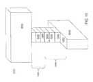
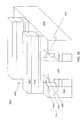
- FIG. 3is a schematic perspective view of multiple PCMS cells arranged in a portion 300 of a cross-point array, according to an embodiment.
- PCMS cellsmay be formed from a fabrication process described above and in further detail below.
- a PCMS cellmay comprise a memory portion 350 adjacent to row lines 340 and a switch portion 360 adjacent to column lines 310 .
- Row lines 340 and column lines 310extending across a plurality of such PCMS cells, may carry electrical signals to/from a memory controller, memory write circuitry, and/or memory read circuitry (not shown) including sense amplifiers, for example.
- Row lines 340may be substantially perpendicular to column lines 310 in a cross-point array, wherein a PCMS cell may be located at intersections of row lines 340 and column lines 310 .
- Memory portion 350may include a memory bottom electrode 353 , a memory phase change material (PCM) 355 , and a top memory electrode 358 .
- Switch portion 360may include a switch bottom electrode 363 , a switch PCM 365 , and a top switch electrode 368 .
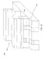
- FIG. 4is a schematic perspective view of multiple PCMS cells arranged in a portion 400 of a cross-point array, according to another embodiment.
- Such PCMS cellsmay be similar to PCMS cells shown in FIG. 3 , for example, except that memory portion 450 may be adjacent to column lines 410 and switch portion 460 may be adjacent to row lines 440 .
- Such PCMS cellsmay be formed from a fabrication process used to fabricate portion 300 , except that particular materials for switch portion 460 may be deposited before those of memory portion 450 , for example.
- row lines 440 and column lines 410may carry electrical signals to/from a memory controller, memory write circuitry and/or memory read circuitry (not shown) including sense amplifiers, for example.
- Row lines 440may be substantially perpendicular to column lines 410 in a cross-point array.
- Memory portion 450may include a memory bottom electrode 453 , a memory PCM 455 , and a top memory electrode 458 .
- Switch portion 460may include a switch bottom electrode 463 , a switch PCM 465 , and a top switch electrode 468 .
- cross-point array portions 300 and 400are merely examples, and claimed subject matter is not so limited.
- FIGS. 5-10are schematic perspective views of PCMS cells, according to different embodiments. Differences between such illustrated embodiments may be directed to whether particular switch and/or memory material layers extend from a memory cell to beyond one or more neighboring memory cells. Thus, such differences may relate to varying degrees of isolation among neighboring PCMS cells, for example. As described in further detail below, applying different etching materials and/or etching times during fabrication processes, for example, may lead to such different embodiments. Also as described in further detail below, whether particular switch and/or memory material layers extend from a memory cell to beyond one or more neighboring memory cells may affect behavior of the memory cells. Such memory cell behavior may involve distribution and/or control of generated heat, electrical current, and/or parasitic memory cell parameters such as capacitance and so on.
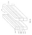
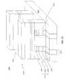
- FIG. 5is a schematic perspective view of a PCMS cell 500 , according to an embodiment.
- a cellmay include at least a portion of row metal 540 and column metal 510 , which may comprise signal lines that extend across a plurality of memory cells in a cross-point memory cell array.
- signal or control linesmay carry electrical signals addressed to one or more particular memory cells and generated by a memory controller during write and/or read processes.
- row metal 540 and column metal 510may comprise an electrically-conducting material such as gold, copper, aluminum, and so on.
- electrically-conducting materialmay comprise a doped semiconductor, though claimed subject matter is not so limited.
- a memory portion 550 adjacent to row metal 540may include a memory bottom electrode 553 , memory PCM 555 , and memory top electrode 558 .
- Memory PCM 555may comprise chalcogenide glass and/or germanium antimony telluride (GST), for example.
- Memory bottom and/or top electrodesmay comprise titanium nitride (TiN), platinum or other noble metals, and/or carbon, just to name a few examples.
- a switch portion 560 adjacent to column metal 510may include a switch bottom electrode 563 , switch PCM 565 , and switch top electrode 568 .
- Switch PCM 565may comprise chalcogenide glass and/or GST, for example.
- Switch bottom and/or top electrodesmay comprise titanium nitride (TiN), platinum or other noble metals, and/or carbon, just to name a few examples.
- Memory bottom electrode 553 , memory PCM 555 , switch PCM 565 , and/or switch top electrode 568may extend from PCMS cell 500 to beyond one or more neighboring memory cells along row metal 540 and column metal 510 , respectively. Accordingly, memory top electrode 558 and/or switch bottom electrode 563 may be isolated from such neighboring memory cells.
- a relatively high density electrical currentmay be generated inside memory top electrode 558 and/or adjacent portions of PCMS 500 that are relatively close to memory top electrode 558 .
- phase change action during operation of PCMS 500may occur near an interface between the memory PCM 555 and the memory top electrode 558 .
- PCMS cell 500are merely examples, and claimed subject matter is not so limited.
- FIG. 6is a schematic perspective view of a PCMS cell 600 , according to an embodiment.
- a cellmay include at least a portion of row metal 640 and column metal 610 , which may comprise signal lines that extend across a plurality of memory cells in a cross-point memory cell array.
- a memory portion 650 adjacent to row metal 640may include a memory bottom electrode 653 , memory PCM 655 , and memory top electrode 658 .
- a switch portion 660 adjacent to column metal 610may include a switch bottom electrode 663 , switch PCM 665 , and switch top electrode 668 .
- Memory bottom electrode 653 , switch PCM 665 , and/or switch top electrode 668may extend from PCMS cell 600 to beyond one or more neighboring memory cells along row metal 640 and column metal 610 , respectively.
- memory PCM 655 , memory top electrode 658 , and/or switch bottom electrode 663may not extend from PCMS cell 600 to beyond one or more neighboring memory cells. Accordingly, memory PCM 655 , memory top electrode 658 , and/or switch bottom electrode 663 may be physically separated and isolated from such neighboring memory cells.
- a relatively high density electrical currentmay be generated inside memory PCM 655 . Thus, heat generation and phase change action during operation of PCMS 600 may occur throughout PCMS 600 .
- materials having particular electrical and/or thermal propertiesmay be selected for top and bottom memory electrodes in order to adjust a temperature profile within PCMS 600 .
- Such adjustmentmay be used in a process to optimize performance of a memory device that includes PCMS 600 .
- PCMS cell 600is merely examples, and claimed subject matter is not so limited.
- FIG. 7is a schematic perspective view of a PCMS cell 700 , according to an embodiment.
- a cellmay include at least a portion of row metal 740 and column metal 710 , which may comprise signal lines that extend across a plurality of memory cells in a cross-point memory cell array.
- a memory portion 750 adjacent to row metal 740may include a memory bottom electrode 753 , memory PCM 755 , and memory top electrode 758 .
- a switch portion 760 adjacent to column metal 710may include a switch bottom electrode 763 , switch PCM 765 , and switch top electrode 768 .
- Switch PCM 765 and/or switch top electrode 768may extend from PCMS cell 700 to beyond one or more neighboring memory cells along column metal 710 .
- memory bottom electrode 753 , memory PCM 755 , memory top electrode 758 , and/or switch bottom electrode 763may not extend from PCMS cell 700 to beyond one or more neighboring memory cells. Accordingly, memory bottom electrode 753 , memory PCM 755 , memory top electrode 758 , and/or switch bottom electrode 763 may be physically separated and be isolated from such neighboring memory cells. A relatively high density electrical current may be generated inside memory PCM 755 , memory top electrode 758 , and/or memory bottom electrode 753 . Electrical current in memory bottom electrode 753 may be relatively isolated among neighboring memory cells, thus providing an improved ability, relative to embodiments described above, for example, to adjust a temperature profile within PCMS 700 by altering electrode material. Of course, such details of PCMS cell 700 are merely examples, and claimed subject matter is not so limited.
- FIG. 8is a schematic perspective view of a PCMS cell 800 , according to an embodiment.
- a cellmay include at least a portion of row metal 840 and column metal 810 , which may comprise signal lines that extend across a plurality of memory cells in a cross-point memory cell array.
- a memory portion 850 adjacent to row metal 840may include a memory bottom electrode 853 , memory PCM 855 , and memory top electrode 858 .
- a switch portion 860 adjacent to column metal 810may include a switch bottom electrode 863 , switch PCM 865 , and switch top electrode 868 .
- Memory bottom electrode 853 and/or memory PCM 855may extend from PCMS cell 800 to beyond one or more neighboring memory cells along row metal 840 .
- memory top electrode 858 , switch bottom electrode 863 , switch PCM 865 , and/or switch top electrode 868may not extend from PCMS cell 800 to beyond one or more neighboring memory cells. Accordingly, memory top electrode 858 , switch bottom electrode 863 , switch PCM 865 , and/or switch top electrode 868 may be physically separated and isolated from such neighboring memory cells.
- PCMS cell 800such details of PCMS cell 800 are merely examples, and claimed subject matter is not so limited.
- FIG. 9is a schematic perspective view of a PCMS cell 900 , according to an embodiment.
- a cellmay include at least a portion of row metal 940 and column metal 910 , which may comprise signal lines that extend across a plurality of memory cells in a cross-point memory cell array.
- a memory portion 950 adjacent to row metal 940may include a memory bottom electrode 953 , memory PCM 955 , and memory top electrode 958 .
- a switch portion 960 adjacent to column metal 910may include a switch bottom electrode 963 , switch PCM 965 , and switch top electrode 968 .
- Memory bottom electrode 953may extend from PCMS cell 900 to beyond one or more neighboring memory cells along row metal 940 .
- memory PCM 955 , memory top electrode 958 , switch bottom electrode 963 , switch PCM 965 , and/or switch top electrode 968may not extend from PCMS cell 900 to beyond one or more neighboring memory cells. Accordingly, memory PCM 955 , memory top electrode 958 , switch bottom electrode 963 , switch PCM 965 , and/or switch top electrode 968 may be physically separated and isolated from such neighboring memory cells.
- PCMS cell 900are merely examples, and claimed subject matter is not so limited.
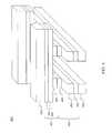
- FIG. 10is a schematic perspective view of a PCMS cell 1000 , according to an embodiment.
- a cellmay include at least a portion of row metal 1040 and column metal 1010 , which may comprise signal lines that extend across a plurality of memory cells in a cross-point memory cell array.
- a memory portion 1050 adjacent to row metal 1040may include a memory bottom electrode 1053 , memory PCM 1055 , and memory top electrode 1058 .
- a switch portion 1060 adjacent to column metal 1010may include a switch bottom electrode 1063 , switch PCM 1065 , and switch top electrode 1068 .
- portions of memory portion 1050 and/or switch portion 1060may not extend from PCMS cell 1000 to beyond one or more neighboring memory cells.
- memory bottom electrode 1053 , memory PCM 1055 , memory top electrode 1058 , switch bottom electrode 1063 , switch PCM 1065 , and/or switch top electrode 1068may not extend from PCMS cell 1000 to beyond one or more neighboring memory cells. Accordingly, memory bottom electrode 1053 , memory PCM 1055 , memory top electrode 1058 , switch bottom electrode 1063 , switch PCM 1065 , and/or switch top electrode 1068 may be physically separated and isolated from such neighboring memory cells.
- PCMS cell 1000are merely examples, and claimed subject matter is not so limited.
- FIG. 11is a flow diagram of a fabrication process 1100 , according to an embodiment.
- a planer composite filmcomprising row metal 1240 , memory bottom electrode 1253 , memory PCM 1255 , memory top electrode 1258 , and either switch bottom electrode or sacrificial material 1263 may be deposited ( FIG. 12 ).
- material for switch bottom electrode or sacrificial material 1263may be relatively resistant to a subsequent chemical-mechanical polish process. Details and benefits of using such a sacrificial material will be described below.
- an etch maskmay be deposited and patterned into set of etch mask lines 1205 , resulting in a masked film stack 1200 shown in FIG. 12 , for example.
- Such an etch maskmay comprise a photoresist, a dielectric, or other material that is relatively easy to etch into a line pattern, for example.
- Patterningmay be performed using photolithography (e.g., direct print, expose/shift/expose, expose/positive develop/negative develop), photolithography with pitch doubling process (e.g., spacers), and imprinting, just to name a few examples.
- an isolation etch of film stack 1200may be performed using a plasma etch process. Such an isolation etch may result in a self-aligned memory device active region and row metal structure, such as that shown in FIG. 13 , for example.
- Adjacent lines 1370which may be separated by isolation trench 1380 , may comprise patterned row metal 1340 , patterned memory bottom electrode 1353 , patterned memory PCM 1355 , patterned memory top electrode 1358 , and either patterned switch bottom electrode or patterned sacrificial material.
- sidewalls of isolation trench 1380may be cleaned using a combination of plasma treatment, a wet chemical process, and/or thin film deposition, for example.
- a subsequent passivation processmay comprise filling isolation trench 1380 with an insulating dielectric material using a deposition process comprising PECVD, CVD, ALD, or spin-on, just to name a few examples. Excess insulating dielectric material may then be removed using a chemical-mechanical polish in order to expose a top of the device structure, resulting in a structure 1400 having insulating material 1420 , such as that shown in FIG. 14 , for example.
- particular switch bottom electrode/sacrificial materialwhich may comprise a top layer of film stack 1200 , for example, may be selected so that film stack layer 1200 may act as a polish stop, thus providing an opportunity to adjust a resulting height of structure 1400 .
- top layer of structure 1400comprises a sacrificial material, such as sacrificial material 1263
- sacrificial materialmay be replaced with another material suitable for bottom switch electrode, as shown in FIG. 15 .
- Such replacementmay be performed using a process involving a plasma etch or a wet etch, replacement material deposition, and a subsequent chemical-mechanical polish.
- Such an optional replacement processmay be used to separate selection of material suitable for a switch device electrode and selection of material suitable for an isolation oxide polish stop.
- a composite film 1650comprising switch PCM 1665 , switch top electrode 1668 , and column metal 1610 may be deposited on structure 1400 .
- an etch maskmay be deposited on top of such a film stack. Patterning such an etch mask into a set of lines 1605 may result in structure 1600 , shown in FIG. 16 , for example.
- process 1100may next include applying an etching process to structure 1600 using lines 1605 as an etch mask. Such an etching process may etch composite film 1650 between lines 1605 to form trenches 1785 between switch devices 1705 , shown in FIG. 17 , for example.
- insulating material 1420may act as an etch stop to such an etch process. Accordingly, such an etch process may terminate at a top of structure 1400 over insulating material 1420 . However, such an etch process may continue to etch portions of structure 1400 between insulating material 1420 , depending, at least in part, on a duration of the etching process.
- memory portion 1750 between insulating material 1420may be etched below an upper surface of insulating material 1420 . Depth of etch of memory portion 1750 may be adjusted in order to etch to various patterned layers of memory portion 1750 . As mentioned above, such an adjustment may be performed by selecting a duration of the etching process, for example. Accordingly, by performing such an adjustment, structure 1600 may be formed into a particular PCMS cell, such as PCMS cells shown in FIGS. 5-10 , as described in further detail below.
- FIG. 17shows a perspective view of structure 1700 , wherein an etching process applied to structure 1600 , such as that described for block 1160 in FIG. 11 , may be used to isolate switch devices 1705 and middle electrodes 1770 comprising a switch bottom electrode 1763 and memory top electrode 1758 , for example, as shown in FIG. 17 .
- etchingmay be terminated after removing the middle electrodes 1770 to form a well 1783 in isolation trench 1780 .
- Resulting structure 1700may comprise PCMS cell 500 , for example
- FIG. 18shows a perspective view of structure 1800 , wherein an etching process applied to structure 1600 , such as that described for block 1160 in FIG. 11 , may be used to isolate switch devices 1805 , middle electrodes 1870 , and memory PCM 1855 .
- switch devicesmay comprise a switch bottom electrode 1863 and memory top electrode 1858 , for example, as shown in FIG. 18 .
- etchingmay be terminated after removing memory PCM 1855 to form a well 1883 in isolation trench 1880 .
- Resulting structure 1800may comprise PCMS cell 600 , for example.
- an additional etching processmay be performed to address a difficulty in removing a relatively large portion of memory PCM from well 1883 inside isolation trench 1880 .
- Such an additional etching processmay include removing a portion 1920 of insulation 1820 in trench 1880 , as shown in FIG. 19 , for example.
- FIG. 20shows a perspective view of structure 2000 , wherein an etching process applied to structure 1600 , such as that described for block 1160 in FIG. 11 , may be used to isolate switch devices 2005 , middle electrodes 2070 , memory PCM 2055 , and memory bottom electrode 2053 .
- switch devicesmay comprise a switch bottom electrode 2063 and memory top electrode 2058 , for example, as shown in FIG. 20 .
- etchingmay be terminated after removing memory bottom electrode 2053 to form a well 2083 in isolation trench 1880 .
- Resulting structure 2000may comprise PCMS cell 700 , for example.
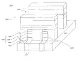
- FIG. 21shows a perspective view of structure 2100 , according to an embodiment.
- Structure 2100may result from a process including cleaning sidewalls of isolation trenches 1880 and adding a passivation material such as by a combination of plasma treatment, wet chemical, and/or thin film deposition, for example.
- a passivation materialsuch as by a combination of plasma treatment, wet chemical, and/or thin film deposition, for example.
- isolation trench 1880 between device structuresmay be filled with insulating dielectric material 2120 .
- a method of filler depositionmay comprise plasma-enhanced chemical vapor deposition (PECVD), chemical vapor deposition (CVD), atomic layer deposition (ALD), and/or a spin-on process, for example.
- PECVDplasma-enhanced chemical vapor deposition
- CVDchemical vapor deposition
- ALDatomic layer deposition
- spin-on processfor example.
- Structure 2100may comprise a portion of a cross-point array, such as that shown in FIGS. 1-3 , for example.
- process 1100is merely examples, and claimed subject matter is not so limited.
- FIG. 22is a schematic diagram illustrating an exemplary embodiment of a computing system 2200 including a memory device 2210 .
- a computing devicemay comprise one or more processors, for example, to execute an application and/or other code.
- memory device 2210may comprise a memory that includes a cross-point array 100 of PCMS cells, shown in FIG. 1 .
- a computing device 2204may be representative of any device, appliance, or machine that may be configurable to manage memory device 2210 .
- Memory device 2210may include a memory controller 2215 and a memory 2222 .
- computing device 2204may include: one or more computing devices and/or platforms, such as, e.g., a desktop computer, a laptop computer, a workstation, a server device, or the like; one or more personal computing or communication devices or appliances, such as, e.g., a personal digital assistant, mobile communication device, or the like; a computing system and/or associated service provider capability, such as, e.g., a database or data storage service provider/system; and/or any combination thereof.
- computing devices and/or platformssuch as, e.g., a desktop computer, a laptop computer, a workstation, a server device, or the like
- personal computing or communication devices or appliancessuch as, e.g., a personal digital assistant, mobile communication device, or the like
- a computing system and/or associated service provider capabilitysuch as, e.g., a database or data storage service provider/system; and/or any combination thereof.
- computing device 2204may include at least one processing unit 2220 that is operatively coupled to memory 2222 through a bus 2240 and a host or memory controller 2215 .
- Processing unit 2220is representative of one or more circuits configurable to perform at least a portion of a data computing procedure or process.
- processing unit 2220may include one or more processors, controllers, microprocessors, microcontrollers, application specific integrated circuits, digital signal processors, programmable logic devices, field programmable gate arrays, and the like, or any combination thereof.
- Processing unit 2220may include an operating system configured to communicate with memory controller 2215 . Such an operating system may, for example, generate commands to be sent to memory controller 2215 over bus 2240 .
- Memory 2222is representative of any data storage mechanism.
- Memory 2222may include, for example, a primary memory 2224 and/or a secondary memory 2226 .
- Primary memory 2224may include, for example, a random access memory, read only memory, etc. While illustrated in this example as being separate from processing unit 2220 , it should be understood that all or part of primary memory 2224 may be provided within or otherwise co-located/coupled with processing unit 2220 .
- Secondary memory 2226may include, for example, the same or similar type of memory as primary memory and/or one or more data storage devices or systems, such as, for example, a disk drive, an optical disc drive, a tape drive, a solid state memory drive, etc.
- secondary memory 2226may be operatively receptive of, or otherwise configurable to couple to, a computer-readable medium 2228 .
- Computer-readable medium 2228may include, for example, any medium that can carry and/or make accessible data, code, and/or instructions for one or more of the devices in system 2200 .
- Computing device 2204may include, for example, an input/output 2232 .
- Input/output 2232is representative of one or more devices or features that may be configurable to accept or otherwise introduce human and/or machine inputs, and/or one or more devices or features that may be configurable to deliver or otherwise provide for human and/or machine outputs.
- input/output device 2232may include an operatively configured display, speaker, keyboard, mouse, trackball, touch screen, data port, etc.
Landscapes
- Engineering & Computer Science (AREA)
- Manufacturing & Machinery (AREA)
- Semiconductor Memories (AREA)
Abstract
Description
Claims (11)
Priority Applications (4)
| Application Number | Priority Date | Filing Date | Title |
|---|---|---|---|
| US13/472,053US8765581B2 (en) | 2009-11-30 | 2012-05-15 | Self-aligned cross-point phase change memory-switch array |
| US14/320,275US9590012B2 (en) | 2009-11-30 | 2014-06-30 | Self-aligned cross-point phase change memory-switch array |
| US15/414,144US10692930B2 (en) | 2009-11-30 | 2017-01-24 | Self-aligned cross-point phase change memory-switch array |
| US16/877,166US11563055B2 (en) | 2009-11-30 | 2020-05-18 | Self-aligned cross-point phase change memory-switch array |
Applications Claiming Priority (2)
| Application Number | Priority Date | Filing Date | Title |
|---|---|---|---|
| US62708009A | 2009-11-30 | 2009-11-30 | |
| US13/472,053US8765581B2 (en) | 2009-11-30 | 2012-05-15 | Self-aligned cross-point phase change memory-switch array |
Related Parent Applications (1)
| Application Number | Title | Priority Date | Filing Date |
|---|---|---|---|
| US62708009ADivision | 2009-11-30 | 2009-11-30 |
Related Child Applications (1)
| Application Number | Title | Priority Date | Filing Date |
|---|---|---|---|
| US14/320,275ContinuationUS9590012B2 (en) | 2009-11-30 | 2014-06-30 | Self-aligned cross-point phase change memory-switch array |
Publications (2)
| Publication Number | Publication Date |
|---|---|
| US20120225534A1 US20120225534A1 (en) | 2012-09-06 |
| US8765581B2true US8765581B2 (en) | 2014-07-01 |
Family
ID=46753581
Family Applications (4)
| Application Number | Title | Priority Date | Filing Date |
|---|---|---|---|
| US13/472,053ActiveUS8765581B2 (en) | 2009-11-30 | 2012-05-15 | Self-aligned cross-point phase change memory-switch array |
| US14/320,275ActiveUS9590012B2 (en) | 2009-11-30 | 2014-06-30 | Self-aligned cross-point phase change memory-switch array |
| US15/414,144Active2030-03-27US10692930B2 (en) | 2009-11-30 | 2017-01-24 | Self-aligned cross-point phase change memory-switch array |
| US16/877,166Active2030-01-21US11563055B2 (en) | 2009-11-30 | 2020-05-18 | Self-aligned cross-point phase change memory-switch array |
Family Applications After (3)
| Application Number | Title | Priority Date | Filing Date |
|---|---|---|---|
| US14/320,275ActiveUS9590012B2 (en) | 2009-11-30 | 2014-06-30 | Self-aligned cross-point phase change memory-switch array |
| US15/414,144Active2030-03-27US10692930B2 (en) | 2009-11-30 | 2017-01-24 | Self-aligned cross-point phase change memory-switch array |
| US16/877,166Active2030-01-21US11563055B2 (en) | 2009-11-30 | 2020-05-18 | Self-aligned cross-point phase change memory-switch array |
Country Status (1)
| Country | Link |
|---|---|
| US (4) | US8765581B2 (en) |
Cited By (11)
| Publication number | Priority date | Publication date | Assignee | Title |
|---|---|---|---|---|
| US20150171321A1 (en)* | 2013-12-13 | 2015-06-18 | Micron Technology, Inc. | Methods of forming metal on inhomogeneous surfaces and structures incorporating metal on inhomogeneous surfaces |
| US9659997B2 (en) | 2014-03-27 | 2017-05-23 | Micron Technology, Inc. | Replacement materials processes for forming cross point memory |
| US9934850B2 (en) | 2013-09-10 | 2018-04-03 | Micron Technology, Inc. | Accessing memory cells in parallel in a cross-point array |
| US10157965B2 (en) | 2014-02-25 | 2018-12-18 | Micron Technology, Inc. | Cross-point memory and methods for fabrication of same |
| US10163982B2 (en) | 2017-03-30 | 2018-12-25 | Intel Corporation | Multi-deck memory device with inverted deck |
| US10164178B2 (en) | 2012-11-21 | 2018-12-25 | Micron Technology, Inc. | Methods for forming narrow vertical pillars and integrated circuit devices having the same |
| US10236444B2 (en) | 2016-08-11 | 2019-03-19 | Samsung Electronics Co., Ltd. | Variable resistance memory device and method of manufacturing the same |
| US10283703B2 (en) | 2014-08-25 | 2019-05-07 | Micron Technology, Inc. | Cross-point memory and methods for forming of the same |
| US10367033B2 (en) | 2013-11-21 | 2019-07-30 | Micron Technology, Inc. | Cross-point memory and methods for fabrication of same |
| US10396125B2 (en) | 2014-11-07 | 2019-08-27 | Micron Technology, Inc. | Cross-point memory and methods for fabrication of same |
| US10854674B2 (en) | 2014-02-25 | 2020-12-01 | Micron Technology, Inc. | Cross-point memory and methods for fabrication of same |
Families Citing this family (34)
| Publication number | Priority date | Publication date | Assignee | Title |
|---|---|---|---|---|
| US9454997B2 (en) | 2010-12-02 | 2016-09-27 | Micron Technology, Inc. | Array of nonvolatile memory cells having at least five memory cells per unit cell, having a plurality of the unit cells which individually comprise three elevational regions of programmable material, and/or having a continuous volume having a combination of a plurality of vertically oriented memory cells and a plurality of horizontally oriented memory cells; array of vertically stacked tiers of nonvolatile memory cells |
| KR102166506B1 (en)* | 2012-12-26 | 2020-10-15 | 소니 세미컨덕터 솔루션즈 가부시키가이샤 | Storage apparatus and method for manufacturing same |
| KR102050502B1 (en) | 2013-03-18 | 2020-01-08 | 삼성전자주식회사 | Hybrid vertical cavity laer and method of manufacturing the same |
| US9997703B2 (en)* | 2013-07-25 | 2018-06-12 | Hewlett Packard Enterprise Development Lp | Resistive memory device having field enhanced features |
| US9257431B2 (en) | 2013-09-25 | 2016-02-09 | Micron Technology, Inc. | Memory cell with independently-sized electrode |
| US9153483B2 (en)* | 2013-10-30 | 2015-10-06 | Taiwan Semiconductor Manufacturing Company, Ltd. | Method of semiconductor integrated circuit fabrication |
| US11223014B2 (en) | 2014-02-25 | 2022-01-11 | Micron Technology, Inc. | Semiconductor structures including liners comprising alucone and related methods |
| US9484196B2 (en) | 2014-02-25 | 2016-11-01 | Micron Technology, Inc. | Semiconductor structures including liners comprising alucone and related methods |
| US10249819B2 (en) | 2014-04-03 | 2019-04-02 | Micron Technology, Inc. | Methods of forming semiconductor structures including multi-portion liners |
| US11133461B2 (en)* | 2014-09-26 | 2021-09-28 | Intel Corporation | Laminate diffusion barriers and related devices and methods |
| US9397145B1 (en)* | 2015-05-14 | 2016-07-19 | Micron Technology, Inc. | Memory structures and related cross-point memory arrays, electronic systems, and methods of forming memory structures |
| US10510957B2 (en)* | 2017-07-26 | 2019-12-17 | Micron Technology, Inc. | Self-aligned memory decks in cross-point memory arrays |
| KR102593112B1 (en) | 2017-10-23 | 2023-10-25 | 삼성전자주식회사 | Variable resistance memory device and method of forming the same |
| US10930705B2 (en) | 2018-03-28 | 2021-02-23 | International Business Machines Corporation | Crystallized silicon vertical diode on BEOL for access device for confined PCM arrays |
| US10693060B2 (en)* | 2018-04-27 | 2020-06-23 | Taiwan Semiconductor Manufacturing Company Ltd. | Phase change memory structure and the same |
| US10892406B2 (en) | 2018-06-04 | 2021-01-12 | Intel Corporation | Phase change memory structures and devices |
| US10541365B1 (en) | 2018-08-15 | 2020-01-21 | Taiwan Semiconductor Manufacturing Co., Ltd. | Phase change memory and method of fabricating same |
| US10803933B2 (en) | 2018-08-21 | 2020-10-13 | International Business Machines Corporation | Self-aligned high density and size adjustable phase change memory |
| KR102722150B1 (en)* | 2019-07-23 | 2024-10-28 | 삼성전자주식회사 | Variable resistance memory devices and methods of manufacturing the same |
| US11404480B2 (en) | 2019-12-26 | 2022-08-02 | Taiwan Semiconductor Manufacturing Company, Ltd. | Memory arrays including continuous line-shaped random access memory strips and method forming same |
| US11282815B2 (en) | 2020-01-14 | 2022-03-22 | Micron Technology, Inc. | Methods of forming microelectronic devices, and related microelectronic devices and electronic systems |
| US11411181B2 (en) | 2020-03-30 | 2022-08-09 | Taiwan Semiconductor Manufacturing Co., Ltd. | Phase-change memory device and method |
| US11355554B2 (en) | 2020-05-08 | 2022-06-07 | Micron Technology, Inc. | Sense lines in three-dimensional memory arrays, and methods of forming the same |
| US11380669B2 (en) | 2020-06-18 | 2022-07-05 | Micron Technology, Inc. | Methods of forming microelectronic devices |
| US11557569B2 (en) | 2020-06-18 | 2023-01-17 | Micron Technology, Inc. | Microelectronic devices including source structures overlying stack structures, and related electronic systems |
| US11699652B2 (en) | 2020-06-18 | 2023-07-11 | Micron Technology, Inc. | Microelectronic devices and electronic systems |
| US11563018B2 (en) | 2020-06-18 | 2023-01-24 | Micron Technology, Inc. | Microelectronic devices, and related methods, memory devices, and electronic systems |
| US11335602B2 (en) | 2020-06-18 | 2022-05-17 | Micron Technology, Inc. | Methods of forming microelectronic devices, and related microelectronic devices and electronic systems |
| US11705367B2 (en) | 2020-06-18 | 2023-07-18 | Micron Technology, Inc. | Methods of forming microelectronic devices, and related microelectronic devices, memory devices, electronic systems, and additional methods |
| US11825658B2 (en) | 2020-08-24 | 2023-11-21 | Micron Technology, Inc. | Methods of forming microelectronic devices and memory devices |
| US11417676B2 (en) | 2020-08-24 | 2022-08-16 | Micron Technology, Inc. | Methods of forming microelectronic devices and memory devices, and related microelectronic devices, memory devices, and electronic systems |
| US11751408B2 (en) | 2021-02-02 | 2023-09-05 | Micron Technology, Inc. | Methods of forming microelectronic devices, and related microelectronic devices, memory devices, and electronic systems |
| US11709553B2 (en) | 2021-02-25 | 2023-07-25 | International Business Machines Corporation | Automated prediction of a location of an object using machine learning |
| US12402329B2 (en)* | 2021-11-03 | 2025-08-26 | International Business Machines Corporation | Top via containing random-access memory cross-bar array |
Citations (10)
| Publication number | Priority date | Publication date | Assignee | Title |
|---|---|---|---|---|
| US4809044A (en) | 1986-08-22 | 1989-02-28 | Energy Conversion Devices, Inc. | Thin film overvoltage protection devices |
| US5845315A (en) | 1995-09-14 | 1998-12-01 | Micron Technology, Inc. | Method and apparatus for reducing the access time of a memory device by decoding a row address during a precharge period of the memory device |
| US20040100828A1 (en) | 2002-11-26 | 2004-05-27 | Garney John I. | Stacked memory device having shared bitlines and method of making the same |
| US20050214953A1 (en)* | 2004-03-29 | 2005-09-29 | Heon Lee | Method of fabricating a mram device |
| US20070297213A1 (en) | 2005-01-18 | 2007-12-27 | Intel Corporation | Forming a carbon layer between phase change layers of a phase change memory |
| US20090194756A1 (en)* | 2008-01-31 | 2009-08-06 | Kau Derchang | Self-aligned eletrode phase change memory |
| US20100008124A1 (en)* | 2008-07-09 | 2010-01-14 | Sandisk 3D Llc | Cross point memory cell with distributed diodes and method of making same |
| US20100163818A1 (en) | 2008-12-30 | 2010-07-01 | Stmicroelectronics S.R.L. | Forming a carbon passivated ovonic threshold switch |
| US20100176368A1 (en)* | 2009-01-14 | 2010-07-15 | Ko Nikka | Method of manufacturing semiconductor memory device, and semiconductor memory device |
| US20110002161A1 (en)* | 2009-07-06 | 2011-01-06 | Seagate Technology Llc | Phase change memory cell with selecting element |
Family Cites Families (9)
| Publication number | Priority date | Publication date | Assignee | Title |
|---|---|---|---|---|
| US6567293B1 (en)* | 2000-09-29 | 2003-05-20 | Ovonyx, Inc. | Single level metal memory cell using chalcogenide cladding |
| US6753561B1 (en)* | 2002-08-02 | 2004-06-22 | Unity Semiconductor Corporation | Cross point memory array using multiple thin films |
| WO2004061851A2 (en)* | 2002-12-19 | 2004-07-22 | Matrix Semiconductor, Inc | An improved method for making high-density nonvolatile memory |
| US7220983B2 (en)* | 2004-12-09 | 2007-05-22 | Macronix International Co., Ltd. | Self-aligned small contact phase-change memory method and device |
| US7846785B2 (en)* | 2007-06-29 | 2010-12-07 | Sandisk 3D Llc | Memory cell that employs a selectively deposited reversible resistance-switching element and methods of forming the same |
| US7824956B2 (en)* | 2007-06-29 | 2010-11-02 | Sandisk 3D Llc | Memory cell that employs a selectively grown reversible resistance-switching element and methods of forming the same |
| KR101097866B1 (en)* | 2008-04-29 | 2011-12-23 | 주식회사 하이닉스반도체 | Method of manufacturing phase change ram device |
| KR100962019B1 (en)* | 2008-06-30 | 2010-06-08 | 주식회사 하이닉스반도체 | Phase change memory device comprising a protective film and method of manufacturing the same |
| US8093576B1 (en) | 2009-11-30 | 2012-01-10 | Micron Technology, Inc. | Chemical-mechanical polish termination layer to build electrical device isolation |
- 2012
- 2012-05-15USUS13/472,053patent/US8765581B2/enactiveActive
- 2014
- 2014-06-30USUS14/320,275patent/US9590012B2/enactiveActive
- 2017
- 2017-01-24USUS15/414,144patent/US10692930B2/enactiveActive
- 2020
- 2020-05-18USUS16/877,166patent/US11563055B2/enactiveActive
Patent Citations (10)
| Publication number | Priority date | Publication date | Assignee | Title |
|---|---|---|---|---|
| US4809044A (en) | 1986-08-22 | 1989-02-28 | Energy Conversion Devices, Inc. | Thin film overvoltage protection devices |
| US5845315A (en) | 1995-09-14 | 1998-12-01 | Micron Technology, Inc. | Method and apparatus for reducing the access time of a memory device by decoding a row address during a precharge period of the memory device |
| US20040100828A1 (en) | 2002-11-26 | 2004-05-27 | Garney John I. | Stacked memory device having shared bitlines and method of making the same |
| US20050214953A1 (en)* | 2004-03-29 | 2005-09-29 | Heon Lee | Method of fabricating a mram device |
| US20070297213A1 (en) | 2005-01-18 | 2007-12-27 | Intel Corporation | Forming a carbon layer between phase change layers of a phase change memory |
| US20090194756A1 (en)* | 2008-01-31 | 2009-08-06 | Kau Derchang | Self-aligned eletrode phase change memory |
| US20100008124A1 (en)* | 2008-07-09 | 2010-01-14 | Sandisk 3D Llc | Cross point memory cell with distributed diodes and method of making same |
| US20100163818A1 (en) | 2008-12-30 | 2010-07-01 | Stmicroelectronics S.R.L. | Forming a carbon passivated ovonic threshold switch |
| US20100176368A1 (en)* | 2009-01-14 | 2010-07-15 | Ko Nikka | Method of manufacturing semiconductor memory device, and semiconductor memory device |
| US20110002161A1 (en)* | 2009-07-06 | 2011-01-06 | Seagate Technology Llc | Phase change memory cell with selecting element |
Cited By (27)
| Publication number | Priority date | Publication date | Assignee | Title |
|---|---|---|---|---|
| US10756265B2 (en) | 2012-11-21 | 2020-08-25 | Micron Technology, Inc. | Methods for forming narrow vertical pillars and integrated circuit devices having the same |
| US10164178B2 (en) | 2012-11-21 | 2018-12-25 | Micron Technology, Inc. | Methods for forming narrow vertical pillars and integrated circuit devices having the same |
| US10971683B2 (en) | 2012-11-21 | 2021-04-06 | Micron Technology, Inc. | Methods for forming narrow vertical pillars and integrated circuit devices having the same |
| US9934850B2 (en) | 2013-09-10 | 2018-04-03 | Micron Technology, Inc. | Accessing memory cells in parallel in a cross-point array |
| US10854287B2 (en) | 2013-09-10 | 2020-12-01 | Micron Technology, Inc. | Accessing memory cells in parallel in a cross-point array |
| US10360975B2 (en) | 2013-09-10 | 2019-07-23 | Micron Technology, Inc. | Accessing memory cells in parallel in a cross-point array |
| US10910437B2 (en) | 2013-11-21 | 2021-02-02 | Micron Technology, Inc. | Cross-point memory and methods for fabrication of same |
| US10367033B2 (en) | 2013-11-21 | 2019-07-30 | Micron Technology, Inc. | Cross-point memory and methods for fabrication of same |
| US10510805B2 (en) | 2013-12-13 | 2019-12-17 | Micron Technology, Inc. | Methods of forming metal on inhomogeneous surfaces and structures incorporating metal on inhomogeneous surfaces |
| US10903276B2 (en) | 2013-12-13 | 2021-01-26 | Micron Technology, Inc. | Methods of forming metal on inhomogeneous surfaces and structures incorporating metal on inhomogeneous surfaces |
| US20150171321A1 (en)* | 2013-12-13 | 2015-06-18 | Micron Technology, Inc. | Methods of forming metal on inhomogeneous surfaces and structures incorporating metal on inhomogeneous surfaces |
| US10854675B2 (en) | 2014-02-25 | 2020-12-01 | Micron Technology, Inc. | Cross-point memory and methods for fabrication of same |
| US11600665B2 (en) | 2014-02-25 | 2023-03-07 | Micron Technology, Inc. | Cross-point memory and methods for fabrication of same |
| US10439001B2 (en) | 2014-02-25 | 2019-10-08 | Micron Technology, Inc. | Cross-point memory and methods for fabrication of same |
| US11011579B2 (en) | 2014-02-25 | 2021-05-18 | Micron Technology, Inc. | Cross-point memory and methods for fabrication of same |
| US10854674B2 (en) | 2014-02-25 | 2020-12-01 | Micron Technology, Inc. | Cross-point memory and methods for fabrication of same |
| US10157965B2 (en) | 2014-02-25 | 2018-12-18 | Micron Technology, Inc. | Cross-point memory and methods for fabrication of same |
| US10475853B2 (en) | 2014-03-27 | 2019-11-12 | Micron Technology, Inc. | Replacement materials processes for forming cross point memory |
| US9659997B2 (en) | 2014-03-27 | 2017-05-23 | Micron Technology, Inc. | Replacement materials processes for forming cross point memory |
| US10050084B2 (en) | 2014-03-27 | 2018-08-14 | Micron Technology, Inc. | Replacement materials processes for forming cross point memory |
| US10283703B2 (en) | 2014-08-25 | 2019-05-07 | Micron Technology, Inc. | Cross-point memory and methods for forming of the same |
| US10680170B2 (en) | 2014-08-25 | 2020-06-09 | Micron Technology, Inc. | Cross-point memory and methods for forming of the same |
| US10396125B2 (en) | 2014-11-07 | 2019-08-27 | Micron Technology, Inc. | Cross-point memory and methods for fabrication of same |
| US10680037B2 (en) | 2014-11-07 | 2020-06-09 | Micron Technology, Inc. | Cross-point memory and methods for fabrication of same |
| US10636968B2 (en) | 2016-08-11 | 2020-04-28 | Samsung Electronics Co., Ltd. | Variable resistance memory device and method of manufacturing the same |
| US10236444B2 (en) | 2016-08-11 | 2019-03-19 | Samsung Electronics Co., Ltd. | Variable resistance memory device and method of manufacturing the same |
| US10163982B2 (en) | 2017-03-30 | 2018-12-25 | Intel Corporation | Multi-deck memory device with inverted deck |
Also Published As
| Publication number | Publication date |
|---|---|
| US20170133433A1 (en) | 2017-05-11 |
| US10692930B2 (en) | 2020-06-23 |
| US11563055B2 (en) | 2023-01-24 |
| US9590012B2 (en) | 2017-03-07 |
| US20200279889A1 (en) | 2020-09-03 |
| US20150001458A1 (en) | 2015-01-01 |
| US20120225534A1 (en) | 2012-09-06 |
Similar Documents
| Publication | Publication Date | Title |
|---|---|---|
| US11563055B2 (en) | Self-aligned cross-point phase change memory-switch array | |
| CN110036479B (en) | Selector of memory cell and doping of memory material | |
| US10163982B2 (en) | Multi-deck memory device with inverted deck | |
| US11322546B2 (en) | Current delivery and spike mitigation in a memory cell array | |
| CN1819297B (en) | Sidewall active pin memory and manufacturing method thereof | |
| US8932897B2 (en) | Phase change memory cell | |
| CN104659206B (en) | Form improved resistive random access memory of voltage characteristic and forming method thereof | |
| CN101013736A (en) | Tubular Phase Change Memory | |
| TW201539731A (en) | Scalable base 矽-based resistive memory device | |
| CN104037187A (en) | One transistor and one resistive (1t1r) random access memory (rram) structure with dual spacers | |
| JP2007073779A (en) | Nonvolatile memory element and its manufacturing method | |
| US9705080B2 (en) | Forming self-aligned conductive lines for resistive random access memories | |
| JP2007273964A (en) | Phase change memory formed using self-aligned process | |
| CN100578753C (en) | Memory element and manufacturing method thereof | |
| US8981330B2 (en) | Thermally-confined spacer PCM cells | |
| CN101981720B (en) | vertical phase change memory cell | |
| CN101136426B (en) | Semiconductor device and method of manufacturing the same | |
| US8093576B1 (en) | Chemical-mechanical polish termination layer to build electrical device isolation | |
| CN102280465A (en) | Resistive random access memory device and manufacturing method thereof | |
| US8067766B2 (en) | Multi-level memory cell | |
| CN116830199A (en) | Two-bit magnetoresistive random access memory device architecture | |
| JP2023521874A (en) | Electronic device containing pillars in arrayed and non-arrayed regions, and related systems and methods | |
| US12219782B2 (en) | Folded access line for memory cell access in a memory device | |
| US11862215B2 (en) | Access line having a resistive layer for memory cell access | |
| TWI757895B (en) | Pillar-shaped cell, manufacturing method thereof and integrated circuit memory device |
Legal Events
| Date | Code | Title | Description |
|---|---|---|---|
| FEPP | Fee payment procedure | Free format text:PAYOR NUMBER ASSIGNED (ORIGINAL EVENT CODE: ASPN); ENTITY STATUS OF PATENT OWNER: LARGE ENTITY | |
| STCF | Information on status: patent grant | Free format text:PATENTED CASE | |
| AS | Assignment | Owner name:U.S. BANK NATIONAL ASSOCIATION, AS COLLATERAL AGENT, CALIFORNIA Free format text:SECURITY INTEREST;ASSIGNOR:MICRON TECHNOLOGY, INC.;REEL/FRAME:038669/0001 Effective date:20160426 Owner name:U.S. BANK NATIONAL ASSOCIATION, AS COLLATERAL AGEN Free format text:SECURITY INTEREST;ASSIGNOR:MICRON TECHNOLOGY, INC.;REEL/FRAME:038669/0001 Effective date:20160426 | |
| AS | Assignment | Owner name:MORGAN STANLEY SENIOR FUNDING, INC., AS COLLATERAL AGENT, MARYLAND Free format text:PATENT SECURITY AGREEMENT;ASSIGNOR:MICRON TECHNOLOGY, INC.;REEL/FRAME:038954/0001 Effective date:20160426 Owner name:MORGAN STANLEY SENIOR FUNDING, INC., AS COLLATERAL Free format text:PATENT SECURITY AGREEMENT;ASSIGNOR:MICRON TECHNOLOGY, INC.;REEL/FRAME:038954/0001 Effective date:20160426 | |
| AS | Assignment | Owner name:U.S. BANK NATIONAL ASSOCIATION, AS COLLATERAL AGENT, CALIFORNIA Free format text:CORRECTIVE ASSIGNMENT TO CORRECT THE REPLACE ERRONEOUSLY FILED PATENT #7358718 WITH THE CORRECT PATENT #7358178 PREVIOUSLY RECORDED ON REEL 038669 FRAME 0001. ASSIGNOR(S) HEREBY CONFIRMS THE SECURITY INTEREST;ASSIGNOR:MICRON TECHNOLOGY, INC.;REEL/FRAME:043079/0001 Effective date:20160426 Owner name:U.S. BANK NATIONAL ASSOCIATION, AS COLLATERAL AGEN Free format text:CORRECTIVE ASSIGNMENT TO CORRECT THE REPLACE ERRONEOUSLY FILED PATENT #7358718 WITH THE CORRECT PATENT #7358178 PREVIOUSLY RECORDED ON REEL 038669 FRAME 0001. ASSIGNOR(S) HEREBY CONFIRMS THE SECURITY INTEREST;ASSIGNOR:MICRON TECHNOLOGY, INC.;REEL/FRAME:043079/0001 Effective date:20160426 | |
| MAFP | Maintenance fee payment | Free format text:PAYMENT OF MAINTENANCE FEE, 4TH YEAR, LARGE ENTITY (ORIGINAL EVENT CODE: M1551) Year of fee payment:4 | |
| AS | Assignment | Owner name:JPMORGAN CHASE BANK, N.A., AS COLLATERAL AGENT, ILLINOIS Free format text:SECURITY INTEREST;ASSIGNORS:MICRON TECHNOLOGY, INC.;MICRON SEMICONDUCTOR PRODUCTS, INC.;REEL/FRAME:047540/0001 Effective date:20180703 Owner name:JPMORGAN CHASE BANK, N.A., AS COLLATERAL AGENT, IL Free format text:SECURITY INTEREST;ASSIGNORS:MICRON TECHNOLOGY, INC.;MICRON SEMICONDUCTOR PRODUCTS, INC.;REEL/FRAME:047540/0001 Effective date:20180703 | |
| AS | Assignment | Owner name:MICRON TECHNOLOGY, INC., IDAHO Free format text:RELEASE BY SECURED PARTY;ASSIGNOR:U.S. BANK NATIONAL ASSOCIATION, AS COLLATERAL AGENT;REEL/FRAME:047243/0001 Effective date:20180629 | |
| AS | Assignment | Owner name:MICRON TECHNOLOGY, INC., IDAHO Free format text:RELEASE BY SECURED PARTY;ASSIGNOR:MORGAN STANLEY SENIOR FUNDING, INC., AS COLLATERAL AGENT;REEL/FRAME:050937/0001 Effective date:20190731 | |
| AS | Assignment | Owner name:MICRON SEMICONDUCTOR PRODUCTS, INC., IDAHO Free format text:RELEASE BY SECURED PARTY;ASSIGNOR:JPMORGAN CHASE BANK, N.A., AS COLLATERAL AGENT;REEL/FRAME:051028/0001 Effective date:20190731 Owner name:MICRON TECHNOLOGY, INC., IDAHO Free format text:RELEASE BY SECURED PARTY;ASSIGNOR:JPMORGAN CHASE BANK, N.A., AS COLLATERAL AGENT;REEL/FRAME:051028/0001 Effective date:20190731 | |
| MAFP | Maintenance fee payment | Free format text:PAYMENT OF MAINTENANCE FEE, 8TH YEAR, LARGE ENTITY (ORIGINAL EVENT CODE: M1552); ENTITY STATUS OF PATENT OWNER: LARGE ENTITY Year of fee payment:8 |