US8762900B2 - Method for proximity correction - Google Patents
Method for proximity correctionDownload PDFInfo
- Publication number
- US8762900B2 US8762900B2US13/534,765US201213534765AUS8762900B2US 8762900 B2US8762900 B2US 8762900B2US 201213534765 AUS201213534765 AUS 201213534765AUS 8762900 B2US8762900 B2US 8762900B2
- Authority
- US
- United States
- Prior art keywords
- design layout
- outer boundary
- modified
- feature
- exposure system
- Prior art date
- Legal status (The legal status is an assumption and is not a legal conclusion. Google has not performed a legal analysis and makes no representation as to the accuracy of the status listed.)
- Active
Links
Images


Classifications
- G—PHYSICS
- G06—COMPUTING OR CALCULATING; COUNTING
- G06F—ELECTRIC DIGITAL DATA PROCESSING
- G06F30/00—Computer-aided design [CAD]
- G06F30/30—Circuit design
- G06F30/39—Circuit design at the physical level
- G06F30/398—Design verification or optimisation, e.g. using design rule check [DRC], layout versus schematics [LVS] or finite element methods [FEM]
- G—PHYSICS
- G03—PHOTOGRAPHY; CINEMATOGRAPHY; ANALOGOUS TECHNIQUES USING WAVES OTHER THAN OPTICAL WAVES; ELECTROGRAPHY; HOLOGRAPHY
- G03F—PHOTOMECHANICAL PRODUCTION OF TEXTURED OR PATTERNED SURFACES, e.g. FOR PRINTING, FOR PROCESSING OF SEMICONDUCTOR DEVICES; MATERIALS THEREFOR; ORIGINALS THEREFOR; APPARATUS SPECIALLY ADAPTED THEREFOR
- G03F1/00—Originals for photomechanical production of textured or patterned surfaces, e.g., masks, photo-masks, reticles; Mask blanks or pellicles therefor; Containers specially adapted therefor; Preparation thereof
- G03F1/36—Masks having proximity correction features; Preparation thereof, e.g. optical proximity correction [OPC] design processes
- G—PHYSICS
- G03—PHOTOGRAPHY; CINEMATOGRAPHY; ANALOGOUS TECHNIQUES USING WAVES OTHER THAN OPTICAL WAVES; ELECTROGRAPHY; HOLOGRAPHY
- G03F—PHOTOMECHANICAL PRODUCTION OF TEXTURED OR PATTERNED SURFACES, e.g. FOR PRINTING, FOR PROCESSING OF SEMICONDUCTOR DEVICES; MATERIALS THEREFOR; ORIGINALS THEREFOR; APPARATUS SPECIALLY ADAPTED THEREFOR
- G03F1/00—Originals for photomechanical production of textured or patterned surfaces, e.g., masks, photo-masks, reticles; Mask blanks or pellicles therefor; Containers specially adapted therefor; Preparation thereof
- G03F1/68—Preparation processes not covered by groups G03F1/20 - G03F1/50
- G03F1/70—Adapting basic layout or design of masks to lithographic process requirements, e.g., second iteration correction of mask patterns for imaging
Definitions
- OPCoptical proximity correction
- FIG. 1is a simplified block diagram of an embodiment of an integrated circuit (IC) manufacturing system and an associated IC manufacturing flow.
- ICintegrated circuit
- FIG. 2is a flowchart of an example method of modifying an IC design layout before mask fabrication according to various aspects of the present disclosure.
- FIG. 3is an example dissection performed on an IC feature.
- FIG. 4is an example of an IC feature after it has undergone optical proximity correction.
- first and second featuresare formed in direct contact
- additional featuresmay be formed between the first and second features, such that the first and second features may not be in direct contact
- FIG. 1is a simplified block diagram of an embodiment of an integrated circuit (IC) manufacturing system 100 and an IC manufacturing flow associated with the IC manufacturing system.
- the IC manufacturing system 100includes a plurality of entities, such as a design house 120 , a mask house 130 , and an IC manufacturer (fab) 150 , that interact with one another in the design, development, and manufacturing cycles and/or services related to manufacturing an integrated circuit (IC) device 160 .
- the plurality of entitiesare connected by a communications network, which may be a single network or a variety of different networks, such as an intranet and the Internet, and may include wired and/or wireless communication channels.
- Each entitymay interact with other entities and may provide services to and/or receive services from the other entities.
- the design house 120 , mask house 130 , and/or IC manufacturer 150may together be parts of a larger corporate entity.
- the design house (or design team) 120generates an IC design layout 122 .
- the IC design layout 122includes various geometrical patterns designed for an IC product, based on a specification of the IC product to be manufactured.
- the geometrical patternscorrespond to patterns of metal, oxide, or semiconductor layers that make up the various components of the IC device 160 to be fabricated.
- the various layerscombine to form various IC features.
- a portion of the IC design layout 122includes various IC features, such as an active region, gate electrode, source and drain, metal lines or vias of an interlayer interconnection, and openings for bonding pads, to be formed in a semiconductor substrate (such as a silicon wafer) and various material layers disposed on the semiconductor substrate.
- the design house 120implements a proper design procedure to form the IC design layout 122 .
- the design proceduremay include logic design, physical design, and/or place and route.
- the IC design layout 122is presented in one or more data files having information of the geometrical patterns.
- the IC design layout 122can be expressed in a GDSII file format (or DFII file format).
- the mask house 130uses the IC design layout 122 to manufacture one or more masks to be used for fabricating the various layers of the IC product according to the IC design layout 122 .
- the mask house 130performs mask data preparation 132 , where the IC design layout 122 is translated into a form that can be physically written by a mask writer, and mask fabrication 144 , where the design layout prepared by the mask data preparation 132 is modified to comply with a particular mask writer and/or mask manufacturer and is then fabricated.
- the mask data preparation 132 and mask fabrication 144are illustrated as separate elements, however, the mask data preparation 132 and mask fabrication 144 can be collectively referred to as mask data preparation.
- the mask data preparation 132includes an optical proximity correction (OPC) and/or an electron proximity correction (OPC/EPC) 138 , and a lithography process check (LPC) 140 .
- OPC/EPC 138is a lithography enhancement technique used to compensate for image errors, such as those that can arise from diffraction, interference, or other process effects.
- OPC/EPC 138may add features, such as scattering bars, serif, and/or hammerheads to the IC design layout 122 according to optical models or rules such that, after a lithography process, a final pattern on a wafer is improved with enhanced resolution and precision.
- Optical proximity checkingaccording to the illustrated embodiment will be described in greater detail below.
- the mask data preparation 132can include further resolution enhancement techniques, such as off-axis illumination, sub-resolution assist features, phase-shifting masks, other suitable techniques, or combinations thereof.
- the LPC 140simulates processing that will be implemented by the IC manufacturer 150 to fabricate the IC device 160 .
- the LPC 140simulates this processing based on the IC design layout 122 to create a simulated manufactured device, such as the IC device 160 .
- the simulated manufactured deviceincludes simulated contours of all or a portion of the IC design layout.
- the LPC 140simulates processing of the modified IC design layout, which has been subjected to the OPC /or EPC 138 .
- the LPC 140uses one or more LPC models (or rules) 142 .
- the LPC models (or rules) 142may be based on actual processing parameters of the IC manufacturer 150 .
- the processing parameterscan include parameters associated with various processes of the IC manufacturing cycle, parameters associated with tools used for manufacturing the IC, and/or other aspects of the manufacturing process.
- LPC 140takes into account various factors, such as aerial image contrast, depth of focus (“DOF”), mask error sensitivity (“MEEF”), other suitable factors, or combinations thereof.
- DOFdepth of focus
- MEEFmask error sensitivity
- the mask data preparation 132may include additional features such as a logic operation (LOP) to modify the IC design layout according to manufacturing rules, a retarget process (RET) to modify the IC design layout to compensate for limitations in lithographic processes used by IC manufacturer 150 , and a mask rule check (MRC) to modify the IC design layout to compensate for limitations during mask fabrication 144 .
- LOPlogic operation
- RETretarget process
- MRCmask rule check
- the processes applied to the IC design layout 122 during data preparation 132may be executed in a variety of different orders.
- a mask or group of masksare fabricated based on the modified IC design layout.
- an electron-beam (e-beam) or a mechanism of multiple e-beamsis used as an exposure source to form a pattern on a mask (photomask or reticle) based on the modified IC design layout.
- the IC manufacturer 150uses the mask (or masks) fabricated by the mask house 130 to fabricate the IC device 160 .
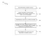
- FIG. 2is a flowchart of a method 200 of modifying an IC design layout before mask fabrication according to various aspects of the present disclosure.
- the method 200may be implemented in the mask data preparation 132 of mask house 130 shown in FIG. 1 .
- the method 200 in FIG. 2is an overview and details associated with each step in the method will be described in association with the subsequent figures in the present disclosure.
- the method 200begins at step 202 by receiving an IC design layout 300 .
- the IC design layout 300is presented in one or more data files having the information of the geometrical patterns.
- the IC design layout 300is expressed in a “GDS” format known in the art.
- the IC design layout 300may be transmitted between the components in IC manufacturing system 100 in alternate file formats such as DFII, CIF, OASIS, or any other suitable file type.
- the IC design layout 300includes various geometrical patterns representing features of an integrated circuit.
- the IC design layout 300may includes main IC features such as active regions, gate electrodes, sources and drains, metal lines, interlayer interconnection vias, and openings for bonding pads that may be formed in a semiconductor substrate (such as a silicon wafer) and various material layers disposed over the semiconductor substrate.
- the IC design layout 300may also include certain assist features, such as those features for imaging effect, processing enhancement, and/or mask identification information.
- FIG. 3illustrates an example IC feature 302 that is a feature contained in the IC design layout 300 .
- the IC feature 302is a gate electrode, but, in alternative embodiments, it may be a interconnection feature or any other IC feature.
- the IC feature 302has an original outer boundary 304 (referred to as a first outer boundary) that defines the shape of the IC feature 302 . Ideally, when the IC feature 302 is formed on the integrated circuit 160 , it will maintain the same shape as defined by the first outer boundary 304 , but this is not always so.
- the method 200proceeds to step 204 by dissecting the IC feature 302 and assigning first target points 310 to the first outer boundary 304 .
- the first outer boundary 304is dissected into multiple discrete segments by a plurality of dissection points (or stitching points) 306 .
- a segmentis a portion of the first outer boundary 304 defined by two adjacent dissection points 306 .
- the first target points 310are assigned to the first outer boundary 304 .
- the first target points 310are utilized in conjunction with the photolithography simulation of the IC feature 302 during LPC 140 .
- the first target points 310are used to determine if the contours of the simulated feature match the first outer boundary 304 .
- a greater or fewer number of the first target points 310may be assigned to the first outer boundary 304 depending on an error tolerance of the final integrated circuit.
- each segmentis associated with a single first target points 310 .
- the method 200proceeds to step 206 by generating a second outer boundary 404 for the IC feature 302 .
- the second outer boundary 404contains one or more rounding corners.
- the second outer boundary 404is generated by employing a convolution of the IC design layout 300 with a predetermined function. Briefly, a convolution is a mathematical algorithm applied on two functions F 1 and F 2 to generate a third function F 3 to show the amount of overlap of one of two functions as it is shifted over by another function.
- the exposure systemis an optical system with a wavelength ( ⁇ ).
- the resolution blur size ⁇can be calculated by (k 1 ⁇ /NA), where k 1 is a constant, ⁇ is the wavelength of photon, and NA is the numerical aperture of the exposure system.
- the predetermined functionincludes a Sinc function in a form of [sin 2 (x/ ⁇ )/(x/ ⁇ ) 2 ] ⁇ [sin 2 (y/ ⁇ )/(y/ ⁇ ) 2 ], where ⁇ is resolution blur size of an exposure system.
- the exposure systemis a charged-particle beam writer.
- the predetermined functionincludes a Gaussian function in a form of exp[ ⁇ x 2 /(2 ⁇ x 2 ) ⁇ y 2 /(2 ⁇ y 2 )], where ⁇ x and ⁇ y is resolution blur size of an exposure system in x direction and y direction, respectively
- the method 200proceeds to step 208 by moving all the first target points 310 from the first outer boundary 304 to the second outer boundary 404 and generating a modified IC design layout 400 containing a modified IC feature 402 .
- the first target points 310are moved inward and outward to the second outer boundary 404 .
- the first target points 310are moved along a direction, which is perpendicular to its original location in the first outer boundary 304 .
- the target points 310is referred to as a second target points 410 for the sake of clarity.
- the modified IC design layout 400contains the modified IC feature 402 having the second outer boundary 404 with the second target points 410 on it and will be used in subsequent pattern correction processes.
- the method 200proceeds to step 210 by performing a proximity correction on the modified IC design layout 400 .
- the proximity correctionincludes an optical proximity correction (OPC).
- OPCoptical proximity correction
- the OPCis utilized to modify the shape of an IC feature to compensate for diffraction or other process effects so that the shape of the feature as formed in the final integrated circuit closely matches the shape of the feature in the IC design layout.
- the OPCmay add various assist features, such as scattering bars, serifs or hammerheads to the modified IC feature 402 .
- the assist featuresmay be placed a distance away from the main feature (such as scattering bars) or be placed adjacent to the main feature (such as serifs and hammerheads).
- the proximity correctionincludes an electron proximity correction (EPC).
- EPCis a compensation process for critical dimensions due to the electron scattering from the wafer substrate.
- the EPC processmay include size bias correction, shape correction, dose correction and background dose equalization (GHOST) correction.
- GHOSTbackground dose equalization
- the method 200further includes performing a photolithography simulation and an error evaluation on the modified IC design layout 400 to define a final IC design layout to be used in the mask fabrication 144 .
- the present disclosureoffers a method for modifying the original IC design layout.
- the methodhas demonstrated to achieve a stable convergence of pattern fidelity in the layout shape correction or dosage correction.
- a method for an integrated circuit (IC) designincludes receiving an IC design layout.
- the IC design layoutincludes an IC feature with a first outer boundary and first target points assigned to the first outer boundary.
- the methodalso includes generating a second outer boundary for the IC feature, moving all the first target points to the second outer boundary to form a modified IC design layout.
- a method for an integrated circuit (IC) design methodincludes receiving an IC design layout having an IC feature with a first outer boundary, assigning first target points to the first outer boundary, applying a convolution on the IC design layout with a predetermined function to generate a second outer boundary of the IC feature, moving all the first target points to the second outer boundary to form a modified IC design layout, performing a proximity correction and a photolithography simulation on the modified IC design layout.
- ICintegrated circuit
- a method for an integrated circuit (IC) design methodincludes receiving an IC design layout having an IC feature with a first outer boundary and first target points on the first outer boundary, generating a second outer boundary of the IC feature by applying a convolution on the IC design layout with a predetermined function, wherein the second outer boundary containing one or more rounding corners, moving all the first target points to the second outer boundary to form a modified IC design layout, performing a proximity correction and a photolithography simulation on the modified IC design layout.
- ICintegrated circuit
Landscapes
- Physics & Mathematics (AREA)
- General Physics & Mathematics (AREA)
- Engineering & Computer Science (AREA)
- Computer Hardware Design (AREA)
- Theoretical Computer Science (AREA)
- Evolutionary Computation (AREA)
- Geometry (AREA)
- General Engineering & Computer Science (AREA)
- Preparing Plates And Mask In Photomechanical Process (AREA)
- Exposure And Positioning Against Photoresist Photosensitive Materials (AREA)
Abstract
Description
The semiconductor integrated circuit (IC) industry has experienced exponential growth. Technological advances in IC design and materials have produced generations of ICs where each generation has scaled down to smaller and more complex circuits than the previous generation. In the course of IC evolution, functional density (i.e., the number of interconnected devices per chip area) has generally increased while geometry size (i.e., the smallest component (or line) that can be created using a fabrication process) has decreased.
This scaling down process generally provides benefits by increasing production efficiency and lowering associated costs. Such scaling down has also increased the complexity of IC processing and manufacturing. For these advances to be realized, similar developments in IC processing and manufacturing are needed. For example an optical proximity correction (OPC) technique is implemented in a mask fabrication. OPC employs a lithographic model to predict contours of the patterns after the lithography process. Before applying a correction, edges of the patterns are dissected into small segments and a target point is defined for each segment. Usually, several iterations are needed in order to achieve a convergence between the edge positions and the target points. A resolution limitation in lithography introduces rounding corners in the contours. A difference between the target point and rounding corner contour causes an unstable correction convergence, which results in a failure of pattern fidelity correction. It is desired to have improvements in this area.
The present disclosure is best understood from the following detailed description when read with the accompanying figures. It is emphasized that, in accordance with the standard practice in the industry, various features are not drawn to scale and are used for illustration purposes only. In fact, the dimensions of the various features may be arbitrarily increased or reduced for clarity of discussion.
It is to be understood that the following disclosure provides many different embodiments, or examples, for implementing different features of the invention. Specific examples of components and arrangements are described below to simplify the present disclosure. These are, of course, merely examples and are not intended to be limiting. Moreover, the performance of a first process before a second process in the description that follows may include embodiments in which the second process is performed immediately after the first process, and may also include embodiments in which additional processes may be performed between the first and second processes. Various features may be arbitrarily drawn in different scales for the sake of simplicity and clarity. Furthermore, the formation of a first feature over or on a second feature in the description that follows may include embodiments in which the first and second features are formed in direct contact, and may also include embodiments in which additional features may be formed between the first and second features, such that the first and second features may not be in direct contact.
The design house (or design team)120 generates anIC design layout 122. TheIC design layout 122 includes various geometrical patterns designed for an IC product, based on a specification of the IC product to be manufactured. The geometrical patterns correspond to patterns of metal, oxide, or semiconductor layers that make up the various components of theIC device 160 to be fabricated. The various layers combine to form various IC features. For example, a portion of theIC design layout 122 includes various IC features, such as an active region, gate electrode, source and drain, metal lines or vias of an interlayer interconnection, and openings for bonding pads, to be formed in a semiconductor substrate (such as a silicon wafer) and various material layers disposed on the semiconductor substrate. Thedesign house 120 implements a proper design procedure to form theIC design layout 122. The design procedure may include logic design, physical design, and/or place and route. TheIC design layout 122 is presented in one or more data files having information of the geometrical patterns. For example, theIC design layout 122 can be expressed in a GDSII file format (or DFII file format).
Themask house 130 uses theIC design layout 122 to manufacture one or more masks to be used for fabricating the various layers of the IC product according to theIC design layout 122. Themask house 130 performsmask data preparation 132, where theIC design layout 122 is translated into a form that can be physically written by a mask writer, andmask fabrication 144, where the design layout prepared by themask data preparation 132 is modified to comply with a particular mask writer and/or mask manufacturer and is then fabricated. In the present embodiment, themask data preparation 132 andmask fabrication 144 are illustrated as separate elements, however, themask data preparation 132 andmask fabrication 144 can be collectively referred to as mask data preparation.
Themask data preparation 132 includes an optical proximity correction (OPC) and/or an electron proximity correction (OPC/EPC)138, and a lithography process check (LPC)140. The OPC/EPC 138 is a lithography enhancement technique used to compensate for image errors, such as those that can arise from diffraction, interference, or other process effects. OPC/EPC 138 may add features, such as scattering bars, serif, and/or hammerheads to theIC design layout 122 according to optical models or rules such that, after a lithography process, a final pattern on a wafer is improved with enhanced resolution and precision. Optical proximity checking according to the illustrated embodiment will be described in greater detail below. Themask data preparation 132 can include further resolution enhancement techniques, such as off-axis illumination, sub-resolution assist features, phase-shifting masks, other suitable techniques, or combinations thereof.
TheLPC 140 simulates processing that will be implemented by theIC manufacturer 150 to fabricate theIC device 160. TheLPC 140 simulates this processing based on theIC design layout 122 to create a simulated manufactured device, such as theIC device 160. The simulated manufactured device includes simulated contours of all or a portion of the IC design layout. In the present embodiment, theLPC 140 simulates processing of the modified IC design layout, which has been subjected to the OPC /orEPC 138. TheLPC 140 uses one or more LPC models (or rules)142. The LPC models (or rules)142 may be based on actual processing parameters of theIC manufacturer 150. The processing parameters can include parameters associated with various processes of the IC manufacturing cycle, parameters associated with tools used for manufacturing the IC, and/or other aspects of the manufacturing process.LPC 140 takes into account various factors, such as aerial image contrast, depth of focus (“DOF”), mask error sensitivity (“MEEF”), other suitable factors, or combinations thereof.
After a simulated device has been created by theLPC 140, if the simulated device is not close enough in shape to satisfy design rules, certain steps in themask data preparation 132, such as OPC/EPC 138, may be repeated to refine theIC design layout 122 further. It should be understood that the above description of themask data preparation 132 has been simplified for the purposes of clarity, and data preparation may include additional features such as a logic operation (LOP) to modify the IC design layout according to manufacturing rules, a retarget process (RET) to modify the IC design layout to compensate for limitations in lithographic processes used byIC manufacturer 150, and a mask rule check (MRC) to modify the IC design layout to compensate for limitations duringmask fabrication 144. Additionally, the processes applied to theIC design layout 122 duringdata preparation 132 may be executed in a variety of different orders.
Aftermask data preparation 132 and duringmask fabrication 144, a mask or group of masks are fabricated based on the modified IC design layout. For example, an electron-beam (e-beam) or a mechanism of multiple e-beams is used as an exposure source to form a pattern on a mask (photomask or reticle) based on the modified IC design layout. TheIC manufacturer 150 uses the mask (or masks) fabricated by themask house 130 to fabricate theIC device 160.
Referring toFIGS. 2 and 3 , themethod 200 begins atstep 202 by receiving anIC design layout 300. TheIC design layout 300 is presented in one or more data files having the information of the geometrical patterns. In one example, theIC design layout 300 is expressed in a “GDS” format known in the art. In alternative embodiments, theIC design layout 300 may be transmitted between the components inIC manufacturing system 100 in alternate file formats such as DFII, CIF, OASIS, or any other suitable file type. TheIC design layout 300 includes various geometrical patterns representing features of an integrated circuit. For example, theIC design layout 300 may includes main IC features such as active regions, gate electrodes, sources and drains, metal lines, interlayer interconnection vias, and openings for bonding pads that may be formed in a semiconductor substrate (such as a silicon wafer) and various material layers disposed over the semiconductor substrate. TheIC design layout 300 may also include certain assist features, such as those features for imaging effect, processing enhancement, and/or mask identification information.
In this regard,FIG. 3 illustrates anexample IC feature 302 that is a feature contained in theIC design layout 300. In one embodiment, theIC feature 302 is a gate electrode, but, in alternative embodiments, it may be a interconnection feature or any other IC feature. The IC feature302 has an original outer boundary304 (referred to as a first outer boundary) that defines the shape of theIC feature 302. Ideally, when theIC feature 302 is formed on theintegrated circuit 160, it will maintain the same shape as defined by the firstouter boundary 304, but this is not always so.
Themethod 200 proceeds to step204 by dissecting theIC feature 302 and assigning first target points310 to the firstouter boundary 304. The firstouter boundary 304 is dissected into multiple discrete segments by a plurality of dissection points (or stitching points)306. A segment is a portion of the firstouter boundary 304 defined by two adjacent dissection points306. Next, the first target points310 are assigned to the firstouter boundary 304. The first target points310 are utilized in conjunction with the photolithography simulation of the IC feature302 duringLPC 140. Specifically, the first target points310 are used to determine if the contours of the simulated feature match the firstouter boundary 304. A greater or fewer number of the first target points310 may be assigned to the firstouter boundary 304 depending on an error tolerance of the final integrated circuit. Further, as shown inFIG. 3 , each segment is associated with a single first target points310.
Referring toFIGS. 2-4 , themethod 200 proceeds to step206 by generating a secondouter boundary 404 for theIC feature 302. In the present embodiment, the secondouter boundary 404 contains one or more rounding corners. The secondouter boundary 404 is generated by employing a convolution of theIC design layout 300 with a predetermined function. Briefly, a convolution is a mathematical algorithm applied on two functions F1and F2to generate a third function F3to show the amount of overlap of one of two functions as it is shifted over by another function. In one embodiment, the exposure system is an optical system with a wavelength (λ). The resolution blur size σ can be calculated by (k1×λ/NA), where k1is a constant, λ is the wavelength of photon, and NA is the numerical aperture of the exposure system. The predetermined function includes a Sinc function in a form of [sin2(x/σ)/(x/σ)2]×[sin2(y/σ)/(y/σ)2], where σ is resolution blur size of an exposure system. In another embodiment, the exposure system is a charged-particle beam writer. The predetermined function includes a Gaussian function in a form of exp[−x2/(2σx2)−y2/(2σy2)], where σxand σyis resolution blur size of an exposure system in x direction and y direction, respectively
Themethod 200 proceeds to step208 by moving all the first target points310 from the firstouter boundary 304 to the secondouter boundary 404 and generating a modifiedIC design layout 400 containing a modifiedIC feature 402. The first target points310 are moved inward and outward to the secondouter boundary 404. For example, the first target points310 are moved along a direction, which is perpendicular to its original location in the firstouter boundary 304. After moving to the second outer boundary, the target points310 is referred to as a second target points410 for the sake of clarity. The modifiedIC design layout 400 contains the modifiedIC feature 402 having the secondouter boundary 404 with the second target points410 on it and will be used in subsequent pattern correction processes.
Themethod 200 proceeds to step210 by performing a proximity correction on the modifiedIC design layout 400. In one embodiment, the proximity correction includes an optical proximity correction (OPC). In general, the OPC is utilized to modify the shape of an IC feature to compensate for diffraction or other process effects so that the shape of the feature as formed in the final integrated circuit closely matches the shape of the feature in the IC design layout. As an example, the OPC may add various assist features, such as scattering bars, serifs or hammerheads to the modifiedIC feature 402. The assist features may be placed a distance away from the main feature (such as scattering bars) or be placed adjacent to the main feature (such as serifs and hammerheads).
In another embodiment, the proximity correction includes an electron proximity correction (EPC). An EPC is a compensation process for critical dimensions due to the electron scattering from the wafer substrate. The EPC process may include size bias correction, shape correction, dose correction and background dose equalization (GHOST) correction.
Themethod 200 further includes performing a photolithography simulation and an error evaluation on the modifiedIC design layout 400 to define a final IC design layout to be used in themask fabrication 144.
Based on the above, it can be seen that the present disclosure offers a method for modifying the original IC design layout. The method has demonstrated to achieve a stable convergence of pattern fidelity in the layout shape correction or dosage correction.
The present disclosure provides many different embodiments of fabricating a semiconductor IC that provide one or more improvements over the prior art. In one embodiment, a method for an integrated circuit (IC) design includes receiving an IC design layout. The IC design layout includes an IC feature with a first outer boundary and first target points assigned to the first outer boundary. The method also includes generating a second outer boundary for the IC feature, moving all the first target points to the second outer boundary to form a modified IC design layout.
In another embodiment, a method for an integrated circuit (IC) design method includes receiving an IC design layout having an IC feature with a first outer boundary, assigning first target points to the first outer boundary, applying a convolution on the IC design layout with a predetermined function to generate a second outer boundary of the IC feature, moving all the first target points to the second outer boundary to form a modified IC design layout, performing a proximity correction and a photolithography simulation on the modified IC design layout.
In yet another embodiment, a method for an integrated circuit (IC) design method includes receiving an IC design layout having an IC feature with a first outer boundary and first target points on the first outer boundary, generating a second outer boundary of the IC feature by applying a convolution on the IC design layout with a predetermined function, wherein the second outer boundary containing one or more rounding corners, moving all the first target points to the second outer boundary to form a modified IC design layout, performing a proximity correction and a photolithography simulation on the modified IC design layout.
The foregoing outlines features of several embodiments so that those skilled in the art may better understand the aspects of the present disclosure. Those skilled in the art should appreciate that they may readily use the present disclosure as a basis for designing or modifying other processes and structures for carrying out the same purposes and/or achieving the same advantages of the embodiments introduced herein. Those skilled in the art should also realize that such equivalent constructions do not depart from the spirit and scope of the present disclosure, and that they may make various changes, substitutions, and alterations herein without departing from the spirit and scope of the present disclosure.
Claims (13)
1. A method for making a mask for an integrated circuit (IC) design, the method comprising:
receiving an IC design layout, the IC design layout including:
an IC feature with a first outer boundary, and
first target points assigned to the first outer boundary;
generating, using a computing system, a second outer boundary for the IC feature;
moving all the first target points to the second outer boundary to form a modified IC design layout; and
providing the modified IC design layout for fabrication of the mask,
wherein the second outer boundary is generated by applying convolution of the IC design layout with a predetermined function, and
wherein the predetermined function includes a Sinc function in a form of [sin2(x/σ)/(x/σ)2]×[sin2(y/σ)/(y/σ)2], where x and y are positions in an x direction and a y direction, respectively, and σ is a resolution blur size of an exposure system.
2. The method ofclaim 1 , wherein the exposure system includes a photon exposure system with a wavelength (λ).
3. The method ofclaim 1 , wherein the resolution blur size is calculated by (k1×λ/NA), where k1is a constant, λ is a wavelength of a photon, and NA is a numerical aperture of the photon exposure system.
4. The method ofclaim 1 , wherein the second outer boundary contains one or more rounding corners.
5. The method ofclaim 1 , wherein the first target points are moved to the second outer boundary in a perpendicular direction to the first outer boundary.
6. The method ofclaim 1 , wherein after moving the first target points to the second outer boundary and forming the modified IC design layout and before providing the modified IC design layout for fabrication, the method further comprising:
performing optical proximity correction (OPC) on the modified IC design layout.
7. The method ofclaim 1 , wherein after moving the first target points to the second outer boundary and forming the modified IC design layout and before providing the modified IC design layout for fabrication, the method further comprising:
performing electron proximity correction (EPC) on the modified IC design layout.
8. The method ofclaim 1 , further comprising:
performing a photolithography simulation on the modified IC design layout; and
performing an error evaluation on the modified IC design layout.
9. A method for making a mask for an integrated circuit (IC) design layout, the method comprising:
receiving the IC design layout having an IC feature with a first outer boundary;
assigning first target points to the first outer boundary;
applying, using a computer, a convolution on the IC design layout with a predetermined function to generate a second outer boundary of the IC feature;
moving the first target points to the second outer boundary to form a modified IC design layout;
performing a proximity correction on the modified IC design layout; and
performing a photolithography simulation on the modified IC design layout, wherein the predetermined function includes a Gaussian function employed in a form of where exp[−x2/(2σx2)−y2/(2σy2)], where x and y are positions in an x direction and a y direction, respectively, and σxand σyis a resolution blur size of an exposure system in the x direction and the y direction, respectively.
10. The method ofclaim 9 , wherein the exposure system includes a charged-particle exposure system.
11. The method ofclaim 9 , wherein the second outer boundary contains one or more rounding corners.
12. A method comprising:
receiving a design layout having a feature, wherein the feature has a first boundary;
assigning a target point to the first boundary;
using a computing system, performing a photolithographic simulation on the design layout to determine a second boundary for the feature, wherein the photolithographic simulation includes performing a mathematical convolution of the design layout with an equation modeling a photolithographic blur of a photolithographic exposure system;
relocating the target point based on the second boundary of the feature; and
providing the design layout having the relocated target point for performing a proximity correction thereupon,
wherein the equation includes at least one of: a Sinc function in a form of [sin2(x/σ)/(x/σ)2]×[sin2(y/σ)/(y/σ)2], where x and y are positions in an x direction and a y direction, respectively, and σ is a resolution blur size of an exposure system, and a Gaussian function employed in a form of exp[−x2/(2σx2)−y2/(2σy2)], where x and y are positions in an x direction and a y direction, respectively, and σxand σyare a resolution blur size of an exposure system in the x direction and the y direction, respectively.
13. The method ofclaim 12 , wherein the assigning of the target point to the first boundary of the feature includes assigning a number of target points to the feature based on an error tolerance.
Priority Applications (3)
| Application Number | Priority Date | Filing Date | Title |
|---|---|---|---|
| US13/534,765US8762900B2 (en) | 2012-06-27 | 2012-06-27 | Method for proximity correction |
| CN201210387301.5ACN103513507B (en) | 2012-06-27 | 2012-10-12 | For the contiguous method revised |
| TW102122906ATWI476509B (en) | 2012-06-27 | 2013-06-27 | Method for making a mask for an integrated circuit design |
Applications Claiming Priority (1)
| Application Number | Priority Date | Filing Date | Title |
|---|---|---|---|
| US13/534,765US8762900B2 (en) | 2012-06-27 | 2012-06-27 | Method for proximity correction |
Publications (2)
| Publication Number | Publication Date |
|---|---|
| US20140007023A1 US20140007023A1 (en) | 2014-01-02 |
| US8762900B2true US8762900B2 (en) | 2014-06-24 |
Family
ID=49779646
Family Applications (1)
| Application Number | Title | Priority Date | Filing Date |
|---|---|---|---|
| US13/534,765ActiveUS8762900B2 (en) | 2012-06-27 | 2012-06-27 | Method for proximity correction |
Country Status (3)
| Country | Link |
|---|---|
| US (1) | US8762900B2 (en) |
| CN (1) | CN103513507B (en) |
| TW (1) | TWI476509B (en) |
Cited By (69)
| Publication number | Priority date | Publication date | Assignee | Title |
|---|---|---|---|---|
| US9449139B2 (en) | 2014-07-03 | 2016-09-20 | Taiwan Semiconductor Manufacturing Company, Ltd. | System and method for tracing a net |
| US9471738B2 (en) | 2015-02-05 | 2016-10-18 | Taiwan Semiconductor Manufacturing Company, Ltd. | Method and apparatus for capacitance extraction |
| US9589764B2 (en) | 2015-03-27 | 2017-03-07 | Taiwan Semiconductor Manufacturing Company, Ltd. | Electron beam lithography process with multiple columns |
| US9625808B2 (en) | 2015-02-13 | 2017-04-18 | Taiwan Semiconductor Manufacturing Company, Ltd. | Durable metal film deposition for mask repair |
| US9632428B2 (en) | 2014-04-15 | 2017-04-25 | Taiwan Semiconductor Manufacturing Company, Ltd. | Method of determining device type and device properties and system of performing the same |
| US9659768B2 (en) | 2014-12-23 | 2017-05-23 | Taiwan Semiconductor Manufacturing Company, Ltd. | Focused radiation beam induced thin film deposition |
| US9672320B2 (en) | 2015-06-30 | 2017-06-06 | Taiwan Semiconductor Manufacturing Company, Ltd. | Method for integrated circuit manufacturing |
| US9679100B2 (en) | 2015-08-21 | 2017-06-13 | Taiwan Semiconductor Manufacturing Company, Ltd. | Environmental-surrounding-aware OPC |
| US9703911B2 (en) | 2015-04-30 | 2017-07-11 | Taiwan Semiconductor Manufacturing Company, Ltd. | Method for library having base cell and VT-related |
| US9741537B1 (en) | 2016-02-19 | 2017-08-22 | Taiwan Semiconductor Manufacturing Co., Ltd. | Method and apparatus for supplying ion beam in ion implantation process |
| US9747408B2 (en) | 2015-08-21 | 2017-08-29 | Taiwan Semiconductor Manufacturing Company, Ltd. | Generating final mask pattern by performing inverse beam technology process |
| US9761411B2 (en) | 2015-01-20 | 2017-09-12 | Taiwain Semiconductor Manufacturing Company, Ltd. | System and method for maskless direct write lithography |
| US9773076B2 (en) | 2014-05-19 | 2017-09-26 | Taiwan Semiconductor Manufacturing Company, Ltd. | Conductive lines in circuits |
| US9793183B1 (en) | 2016-07-29 | 2017-10-17 | Taiwan Semiconductor Manufacturing Co., Ltd. | System and method for measuring and improving overlay using electronic microscopic imaging and digital processing |
| US9805154B2 (en) | 2015-05-15 | 2017-10-31 | Taiwan Semiconductor Manufacturing Company, Ltd. | Method of lithography process with inserting scattering bars |
| US9835680B2 (en) | 2015-03-16 | 2017-12-05 | Taiwan Semiconductor Manufacturing Company, Ltd. | Method, device and computer program product for circuit testing |
| US9892224B2 (en) | 2015-02-12 | 2018-02-13 | Taiwan Semiconductor Manufacturing Company, Ltd. | Method of forming masks |
| US9899190B2 (en) | 2013-11-25 | 2018-02-20 | Taiwan Semiconductor Manufacturing Company, Ltd. | Method and apparatus for transferring pixel data for electron beam lithography |
| US9915866B2 (en) | 2015-11-16 | 2018-03-13 | Taiwan Semiconductor Manufacturing Co., Ltd. | Focused radiation beam induced deposition |
| US9940424B2 (en) | 2016-05-25 | 2018-04-10 | Taiwan Semiconductor Manufacturing Co., Ltd. | Systems and methods for minimum-implant-area aware detailed placement |
| US9946827B2 (en) | 2015-07-16 | 2018-04-17 | Taiwan Semiconductor Manufacturing Company, Ltd. | Method and structure for mandrel and spacer patterning |
| US9953122B2 (en) | 2016-07-14 | 2018-04-24 | Taiwan Semiconductor Manufacturing Company Ltd. | Integrated circuit design method and associated non-transitory computer-readable medium |
| US9960013B2 (en) | 2016-01-13 | 2018-05-01 | Taiwan Semiconductor Manufacturing Company, Ltd. | Continuous writing of pattern |
| US9990460B2 (en) | 2016-09-30 | 2018-06-05 | Taiwan Semiconductor Manufacturing Co., Ltd. | Source beam optimization method for improving lithography printability |
| US10001698B2 (en) | 2015-12-15 | 2018-06-19 | Taiwan Semiconductor Manufacturing Company, Ltd | Layout hierachical structure defined in polar coordinate |
| US10049851B2 (en) | 2016-04-29 | 2018-08-14 | Taiwan Semiconductor Manufacturing Co., Ltd. | Data processing of electron beam lithography system |
| US10078718B2 (en) | 2015-12-30 | 2018-09-18 | Taiwan Semiconductor Manufacturing Co., Ltd. | Multiple patterning method for semiconductor devices |
| US10089433B2 (en) | 2016-05-03 | 2018-10-02 | Taiwan Semiconductor Manufacturing Co., Ltd. | Method for triple-patterning friendly placement |
| US10108764B2 (en) | 2016-04-15 | 2018-10-23 | Taiwan Semiconductor Manufacturing Company, Ltd. | Power consumption estimation method for system on chip (SOC), system for implementing the method |
| US10151971B2 (en) | 2016-07-01 | 2018-12-11 | Taiwan Semiconductor Manufacturing Company, Ltd. | System for and method of seeding an optical proximity correction (OPC) process |
| US10162929B2 (en) | 2016-05-03 | 2018-12-25 | Taiwan Semiconductor Manufacturing Co., Ltd. | Systems and methods for using multiple libraries with different cell pre-coloring |
| US10176284B2 (en) | 2016-09-30 | 2019-01-08 | Taiwan Semiconductor Manufacturing Company Ltd. | Semiconductor circuit design and manufacture method |
| US10276426B2 (en) | 2016-05-31 | 2019-04-30 | Taiwan Semiconductor Manufacturing Co., Ltd. | System and method for performing spin dry etching |
| US10276375B2 (en) | 2016-11-18 | 2019-04-30 | Taiwan Semiconductor Manufacturing Co., Ltd. | Assistant pattern for measuring critical dimension of main pattern in semiconductor manufacturing |
| US10283496B2 (en) | 2016-06-30 | 2019-05-07 | Taiwan Semiconductor Manufacturing Co., Ltd. | Integrated circuit filler and method thereof |
| US10360339B2 (en) | 2014-04-25 | 2019-07-23 | Taiwan Semiconductor Manufacturing Company, Ltd. | Method for integrated circuit manufacturing |
| US10366200B2 (en) | 2016-09-07 | 2019-07-30 | Taiwan Semiconductor Manufacturing Company, Ltd. | System for and method of manufacturing a layout design of an integrated circuit |
| US10396063B2 (en) | 2016-05-31 | 2019-08-27 | Taiwan Semiconductor Manufacturing Company Ltd. | Circuit with combined cells and method for manufacturing the same |
| US10430544B2 (en) | 2016-09-02 | 2019-10-01 | Taiwan Semiconductor Manufacturing Co., Ltd. | Multi-patterning graph reduction and checking flow method |
| US10460070B2 (en) | 2016-01-28 | 2019-10-29 | Taiwan Semiconductor Manufacturing Co., Ltd. | Optimized electromigration analysis |
| US10466586B2 (en) | 2016-11-29 | 2019-11-05 | Taiwan Semiconductor Manufacturing Co., Ltd. | Method of modeling a mask having patterns with arbitrary angles |
| US10475700B2 (en) | 2017-08-31 | 2019-11-12 | Taiwan Semiconductor Manufacturing Company, Ltd. | Etching to reduce line wiggling |
| US10489547B2 (en) | 2016-09-08 | 2019-11-26 | Taiwan Semiconductor Manufacturing Company, Ltd. | Multiple patterning method, system for implementing the method and layout formed |
| US10495967B2 (en) | 2017-09-28 | 2019-12-03 | Taiwan Semiconductor Manufacturing Co., Ltd. | Method of mask simulation model for OPC and mask making |
| US10509882B2 (en) | 2016-08-09 | 2019-12-17 | Taiwan Semiconductor Manufacturing Co., Ltd. | Systems and methods for cell abutment |
| US10514613B2 (en) | 2016-11-28 | 2019-12-24 | Taiwan Semiconductor Manufacturing Co., Ltd. | Pattern modification and patterning process |
| US10521545B2 (en) | 2016-04-15 | 2019-12-31 | Taiwan Semiconductor Manufacturing Co., Ltd. | Placement constraint method for multiple patterning of cell-based chip design |
| US10520829B2 (en) | 2017-09-26 | 2019-12-31 | Taiwan Semiconductor Manufacturing Co., Ltd. | Optical proximity correction methodology using underlying layer information |
| US10521538B2 (en) | 2016-04-27 | 2019-12-31 | Taiwan Semiconductor Manufacturing Co., Ltd | Method and system for integrated circuit design with on-chip variation and spatial correlation |
| US10527928B2 (en) | 2016-12-20 | 2020-01-07 | Taiwan Semiconductor Manufacturing Co., Ltd. | Optical proximity correction methodology using pattern classification for target placement |
| US10671786B2 (en) | 2016-11-29 | 2020-06-02 | Taiwan Semiconductor Manufacturing Co., Ltd. | Method of modeling a mask by taking into account of mask pattern edge interaction |
| US10671052B2 (en) | 2017-11-15 | 2020-06-02 | Taiwan Semiconductor Manufacturing Co., Ltd. | Synchronized parallel tile computation for large area lithography simulation |
| US10685950B2 (en) | 2017-06-29 | 2020-06-16 | Taiwan Semiconductor Manufacturing Co., Ltd. | Photomask design for generating plasmonic effect |
| US10816893B2 (en) | 2016-05-31 | 2020-10-27 | Csmc Technologies Fab2 Co., Ltd. | Method and system for correction of optical proximity effect |
| US10859922B1 (en) | 2019-07-18 | 2020-12-08 | Taiwan Semiconductor Manufacturing Company, Ltd. | Lithography system and method |
| US10866508B2 (en) | 2018-05-18 | 2020-12-15 | Taiwan Semiconductor Manufacturing Company Ltd. | Method for manufacturing photomask and semiconductor manufacturing method thereof |
| US10867805B2 (en) | 2018-06-29 | 2020-12-15 | Taiwan Semiconductor Manufacturing Co., Ltd. | Selective removal of an etching stop layer for improving overlay shift tolerance |
| US10908494B2 (en) | 2017-05-31 | 2021-02-02 | Taiwan Semiconductor Manufacturing Company, Ltd. | Photomask and manufacturing method thereof |
| US11054742B2 (en) | 2018-06-15 | 2021-07-06 | Taiwan Semiconductor Manufacturing Co., Ltd. | EUV metallic resist performance enhancement via additives |
| US11069526B2 (en) | 2018-06-27 | 2021-07-20 | Taiwan Semiconductor Manufacturing Co., Ltd. | Using a self-assembly layer to facilitate selective formation of an etching stop layer |
| US11099478B2 (en) | 2018-08-14 | 2021-08-24 | Taiwan Semiconductor Manufacturing Co., Ltd. | Photomask having recessed region |
| US11172142B2 (en) | 2018-09-25 | 2021-11-09 | Taiwan Semiconductor Manufacturing Co., Ltd. | Image sensor for sensing LED light with reduced flickering |
| US11209728B2 (en) | 2018-06-27 | 2021-12-28 | Taiwan Semiconductor Manufacturing Company Ltd. | Mask and method for fabricating the same |
| US11244858B2 (en) | 2017-08-31 | 2022-02-08 | Taiwan Semiconductor Manufacturing Company, Ltd. | Etching to reduce line wiggling |
| US11262658B2 (en) | 2020-04-28 | 2022-03-01 | Taiwan Semiconductor Manufacturing Company, Ltd. | Photomask, photolithography system and manufacturing process |
| US11289376B2 (en) | 2019-07-31 | 2022-03-29 | Taiwan Semiconductor Manufacturing Co., Ltd | Methods for forming self-aligned interconnect structures |
| US11308254B2 (en) | 2019-08-30 | 2022-04-19 | Taiwan Semiconductor Manufacturing Company Ltd. | Method and system for reducing layout distortion due to exposure non-uniformity |
| US11682647B2 (en) | 2020-04-01 | 2023-06-20 | Taiwan Semiconductor Manufacturing Company, Ltd. | Semiconductor package and method for manufacturing the same |
| US12009400B2 (en) | 2021-02-14 | 2024-06-11 | Taiwan Semiconductor Manufacturing Company, Ltd. | Device providing multiple threshold voltages and methods of making the same |
Families Citing this family (10)
| Publication number | Priority date | Publication date | Assignee | Title |
|---|---|---|---|---|
| CN104865788B (en)* | 2015-06-07 | 2019-05-31 | 上海华虹宏力半导体制造有限公司 | A kind of lithography layout OPC method |
| CN108121830A (en)* | 2016-11-28 | 2018-06-05 | 深圳市中兴微电子技术有限公司 | A kind of manufacturing method of chip and its device |
| US11604451B2 (en) | 2018-12-22 | 2023-03-14 | D2S, Inc. | Method and system of reducing charged particle beam write time |
| US10884395B2 (en) | 2018-12-22 | 2021-01-05 | D2S, Inc. | Method and system of reducing charged particle beam write time |
| US20230124768A1 (en) | 2019-05-24 | 2023-04-20 | D2S, Inc. | Method and system for determining a charged particle beam exposure for a local pattern density |
| US10748744B1 (en) | 2019-05-24 | 2020-08-18 | D2S, Inc. | Method and system for determining a charged particle beam exposure for a local pattern density |
| US11756765B2 (en) | 2019-05-24 | 2023-09-12 | D2S, Inc. | Method and system for determining a charged particle beam exposure for a local pattern density |
| KR20250133977A (en)* | 2020-06-03 | 2025-09-09 | 에이에스엠엘 네델란즈 비.브이. | Systems, products, and methods for generating patterning devices and patterns therefor |
| KR20220080768A (en)* | 2020-12-07 | 2022-06-15 | 삼성전자주식회사 | Error verifying method for optical proximity correction model |
| JP2023045120A (en)* | 2021-09-21 | 2023-04-03 | キオクシア株式会社 | Mask design method and recording medium for the same |
Citations (4)
| Publication number | Priority date | Publication date | Assignee | Title |
|---|---|---|---|---|
| US6430737B1 (en)* | 2000-07-10 | 2002-08-06 | Mentor Graphics Corp. | Convergence technique for model-based optical and process correction |
| US20070006118A1 (en)* | 2000-12-01 | 2007-01-04 | Synopsys Inc. | Displacing Edge Segments On A Fabrication Layout Based On Proximity Effects Model Amplitudes For Correcting Proximity Effects |
| US20080178140A1 (en) | 2007-01-18 | 2008-07-24 | United Microelectronics Corp. | Method for correcting photomask pattern |
| US20090307649A1 (en)* | 2008-06-10 | 2009-12-10 | Dipankar Pramanik | System and method for modifying a data set of a photomask |
Family Cites Families (3)
| Publication number | Priority date | Publication date | Assignee | Title |
|---|---|---|---|---|
| US7784019B1 (en)* | 2006-11-01 | 2010-08-24 | Cadence Design Systems, Inc. | Yield based retargeting for semiconductor design flow |
| CN101750878B (en)* | 2008-12-22 | 2011-12-07 | 中芯国际集成电路制造(上海)有限公司 | optical proximity correction method |
| CN102135725B (en)* | 2011-03-20 | 2012-07-04 | 北京理工大学 | Method for acquiring total number of cut rectangles of PBOPC (Pixel-Based Optical Proximity Correction) optimal mask pattern |
- 2012
- 2012-06-27USUS13/534,765patent/US8762900B2/enactiveActive
- 2012-10-12CNCN201210387301.5Apatent/CN103513507B/enactiveActive
- 2013
- 2013-06-27TWTW102122906Apatent/TWI476509B/enactive
Patent Citations (4)
| Publication number | Priority date | Publication date | Assignee | Title |
|---|---|---|---|---|
| US6430737B1 (en)* | 2000-07-10 | 2002-08-06 | Mentor Graphics Corp. | Convergence technique for model-based optical and process correction |
| US20070006118A1 (en)* | 2000-12-01 | 2007-01-04 | Synopsys Inc. | Displacing Edge Segments On A Fabrication Layout Based On Proximity Effects Model Amplitudes For Correcting Proximity Effects |
| US20080178140A1 (en) | 2007-01-18 | 2008-07-24 | United Microelectronics Corp. | Method for correcting photomask pattern |
| US20090307649A1 (en)* | 2008-06-10 | 2009-12-10 | Dipankar Pramanik | System and method for modifying a data set of a photomask |
Cited By (117)
| Publication number | Priority date | Publication date | Assignee | Title |
|---|---|---|---|---|
| US9899190B2 (en) | 2013-11-25 | 2018-02-20 | Taiwan Semiconductor Manufacturing Company, Ltd. | Method and apparatus for transferring pixel data for electron beam lithography |
| US9632428B2 (en) | 2014-04-15 | 2017-04-25 | Taiwan Semiconductor Manufacturing Company, Ltd. | Method of determining device type and device properties and system of performing the same |
| US10747938B2 (en) | 2014-04-25 | 2020-08-18 | Taiwan Semiconductor Manufacturing Company, Ltd. | Method for integrated circuit manufacturing |
| US10360339B2 (en) | 2014-04-25 | 2019-07-23 | Taiwan Semiconductor Manufacturing Company, Ltd. | Method for integrated circuit manufacturing |
| US9773076B2 (en) | 2014-05-19 | 2017-09-26 | Taiwan Semiconductor Manufacturing Company, Ltd. | Conductive lines in circuits |
| US10360314B2 (en) | 2014-05-19 | 2019-07-23 | Taiwan Semiconductor Manufacturing Company, Ltd. | Method of forming conductive lines in circuits |
| US11106835B2 (en) | 2014-05-19 | 2021-08-31 | Taiwan Semiconductor Manufacturing Company, Ltd. | Method of manufacturing conductive lines in a circuit |
| US12165972B2 (en) | 2014-05-19 | 2024-12-10 | Taiwan Semiconductor Manufacturing Company, Ltd. | Method of manufacturing conductive lines in a circuit |
| US9449139B2 (en) | 2014-07-03 | 2016-09-20 | Taiwan Semiconductor Manufacturing Company, Ltd. | System and method for tracing a net |
| US9659768B2 (en) | 2014-12-23 | 2017-05-23 | Taiwan Semiconductor Manufacturing Company, Ltd. | Focused radiation beam induced thin film deposition |
| US9761411B2 (en) | 2015-01-20 | 2017-09-12 | Taiwain Semiconductor Manufacturing Company, Ltd. | System and method for maskless direct write lithography |
| US9471738B2 (en) | 2015-02-05 | 2016-10-18 | Taiwan Semiconductor Manufacturing Company, Ltd. | Method and apparatus for capacitance extraction |
| US9892224B2 (en) | 2015-02-12 | 2018-02-13 | Taiwan Semiconductor Manufacturing Company, Ltd. | Method of forming masks |
| US9625808B2 (en) | 2015-02-13 | 2017-04-18 | Taiwan Semiconductor Manufacturing Company, Ltd. | Durable metal film deposition for mask repair |
| US9835680B2 (en) | 2015-03-16 | 2017-12-05 | Taiwan Semiconductor Manufacturing Company, Ltd. | Method, device and computer program product for circuit testing |
| US9589764B2 (en) | 2015-03-27 | 2017-03-07 | Taiwan Semiconductor Manufacturing Company, Ltd. | Electron beam lithography process with multiple columns |
| US9703911B2 (en) | 2015-04-30 | 2017-07-11 | Taiwan Semiconductor Manufacturing Company, Ltd. | Method for library having base cell and VT-related |
| US9805154B2 (en) | 2015-05-15 | 2017-10-31 | Taiwan Semiconductor Manufacturing Company, Ltd. | Method of lithography process with inserting scattering bars |
| US9672320B2 (en) | 2015-06-30 | 2017-06-06 | Taiwan Semiconductor Manufacturing Company, Ltd. | Method for integrated circuit manufacturing |
| US12412016B2 (en) | 2015-07-16 | 2025-09-09 | Taiwan Semiconductor Manufacturing Company, Ltd. | Method and structure for mandrel and spacer patterning |
| US9946827B2 (en) | 2015-07-16 | 2018-04-17 | Taiwan Semiconductor Manufacturing Company, Ltd. | Method and structure for mandrel and spacer patterning |
| US11010526B2 (en) | 2015-07-16 | 2021-05-18 | Taiwan Semiconductor Manufacturing Company, Ltd. | Method and structure for mandrel and spacer patterning |
| US10521541B2 (en) | 2015-07-16 | 2019-12-31 | Taiwan Semiconductor Manufacturing Company, Ltd. | Method and structure for mandrel and spacer patterning |
| US11748540B2 (en) | 2015-07-16 | 2023-09-05 | Taiwan Semiconductor Manufacturing Company, Ltd. | Method and structure for mandrel and spacer patterning |
| US9747408B2 (en) | 2015-08-21 | 2017-08-29 | Taiwan Semiconductor Manufacturing Company, Ltd. | Generating final mask pattern by performing inverse beam technology process |
| US9679100B2 (en) | 2015-08-21 | 2017-06-13 | Taiwan Semiconductor Manufacturing Company, Ltd. | Environmental-surrounding-aware OPC |
| US10036948B2 (en) | 2015-08-21 | 2018-07-31 | Taiwan Semiconductor Manufacturing Company, Ltd. | Environmental-surrounding-aware OPC |
| US10061193B2 (en) | 2015-11-16 | 2018-08-28 | Taiwan Semiconductor Manufacturing Co., Ltd. | Focused radiation beam induced deposition |
| US9915866B2 (en) | 2015-11-16 | 2018-03-13 | Taiwan Semiconductor Manufacturing Co., Ltd. | Focused radiation beam induced deposition |
| US10001698B2 (en) | 2015-12-15 | 2018-06-19 | Taiwan Semiconductor Manufacturing Company, Ltd | Layout hierachical structure defined in polar coordinate |
| US10078718B2 (en) | 2015-12-30 | 2018-09-18 | Taiwan Semiconductor Manufacturing Co., Ltd. | Multiple patterning method for semiconductor devices |
| US10817635B2 (en) | 2015-12-30 | 2020-10-27 | Taiwan Semiconductor Manufacturing Co., Ltd. | Multiple patterning method for semiconductor devices |
| US9960013B2 (en) | 2016-01-13 | 2018-05-01 | Taiwan Semiconductor Manufacturing Company, Ltd. | Continuous writing of pattern |
| US10460070B2 (en) | 2016-01-28 | 2019-10-29 | Taiwan Semiconductor Manufacturing Co., Ltd. | Optimized electromigration analysis |
| US9741537B1 (en) | 2016-02-19 | 2017-08-22 | Taiwan Semiconductor Manufacturing Co., Ltd. | Method and apparatus for supplying ion beam in ion implantation process |
| US10108764B2 (en) | 2016-04-15 | 2018-10-23 | Taiwan Semiconductor Manufacturing Company, Ltd. | Power consumption estimation method for system on chip (SOC), system for implementing the method |
| US10521545B2 (en) | 2016-04-15 | 2019-12-31 | Taiwan Semiconductor Manufacturing Co., Ltd. | Placement constraint method for multiple patterning of cell-based chip design |
| US10521538B2 (en) | 2016-04-27 | 2019-12-31 | Taiwan Semiconductor Manufacturing Co., Ltd | Method and system for integrated circuit design with on-chip variation and spatial correlation |
| US10860769B2 (en) | 2016-04-27 | 2020-12-08 | Taiwan Semiconductor Manufacturing Co., Ltd. | Method and system for integrated circuit design with on-chip variation and spatial correlation |
| US10446358B2 (en) | 2016-04-29 | 2019-10-15 | Taiwan Semiconductor Manufacturing Co., Ltd | Data processing of electron beam lithography system |
| US10804066B2 (en) | 2016-04-29 | 2020-10-13 | Taiwan Semiconductor Manufacturing Co., Ltd. | Data processing of electron beam lithography system |
| US10049851B2 (en) | 2016-04-29 | 2018-08-14 | Taiwan Semiconductor Manufacturing Co., Ltd. | Data processing of electron beam lithography system |
| US10089433B2 (en) | 2016-05-03 | 2018-10-02 | Taiwan Semiconductor Manufacturing Co., Ltd. | Method for triple-patterning friendly placement |
| US10162929B2 (en) | 2016-05-03 | 2018-12-25 | Taiwan Semiconductor Manufacturing Co., Ltd. | Systems and methods for using multiple libraries with different cell pre-coloring |
| US9940424B2 (en) | 2016-05-25 | 2018-04-10 | Taiwan Semiconductor Manufacturing Co., Ltd. | Systems and methods for minimum-implant-area aware detailed placement |
| US10276426B2 (en) | 2016-05-31 | 2019-04-30 | Taiwan Semiconductor Manufacturing Co., Ltd. | System and method for performing spin dry etching |
| US11854861B2 (en) | 2016-05-31 | 2023-12-26 | Taiwan Semiconductor Manufacturing Co., Ltd. | System and method for performing spin dry etching |
| US10396063B2 (en) | 2016-05-31 | 2019-08-27 | Taiwan Semiconductor Manufacturing Company Ltd. | Circuit with combined cells and method for manufacturing the same |
| US10816893B2 (en) | 2016-05-31 | 2020-10-27 | Csmc Technologies Fab2 Co., Ltd. | Method and system for correction of optical proximity effect |
| US11309307B2 (en) | 2016-06-30 | 2022-04-19 | Taiwan Semiconductor Manufacturing Co., Ltd. | Integrated circuit filler and method thereof |
| US10388645B2 (en) | 2016-06-30 | 2019-08-20 | Taiwan Semiconductor Manufacturing Co., Ltd. | Integrated circuit filler and method thereof |
| US10679980B2 (en) | 2016-06-30 | 2020-06-09 | Taiwan Semiconductor Manufacturing Co., Ltd. | Integrated circuit filler and method thereof |
| US12183729B2 (en) | 2016-06-30 | 2024-12-31 | Taiwan Semiconductor Manufacturing Co., Ltd. | Integrated circuit filler and method thereof |
| US11776948B2 (en) | 2016-06-30 | 2023-10-03 | Taiwan Semiconductor Manufacturing Co., Ltd. | Integrated circuit filler and method thereof |
| US10283496B2 (en) | 2016-06-30 | 2019-05-07 | Taiwan Semiconductor Manufacturing Co., Ltd. | Integrated circuit filler and method thereof |
| US10151971B2 (en) | 2016-07-01 | 2018-12-11 | Taiwan Semiconductor Manufacturing Company, Ltd. | System for and method of seeding an optical proximity correction (OPC) process |
| US9953122B2 (en) | 2016-07-14 | 2018-04-24 | Taiwan Semiconductor Manufacturing Company Ltd. | Integrated circuit design method and associated non-transitory computer-readable medium |
| US9793183B1 (en) | 2016-07-29 | 2017-10-17 | Taiwan Semiconductor Manufacturing Co., Ltd. | System and method for measuring and improving overlay using electronic microscopic imaging and digital processing |
| US10424519B2 (en) | 2016-07-29 | 2019-09-24 | Taiwan Semiconductor Manufacturing Co., Ltd. | System and method for measuring and improving overlay using electronic microscopic imaging and digital processing |
| US10734294B2 (en) | 2016-07-29 | 2020-08-04 | Taiwan Semiconductor Manufacturing Co., Ltd. | System and method for measuring and improving overlay using electronic microscopic imaging and digital processing |
| US10509882B2 (en) | 2016-08-09 | 2019-12-17 | Taiwan Semiconductor Manufacturing Co., Ltd. | Systems and methods for cell abutment |
| US10430544B2 (en) | 2016-09-02 | 2019-10-01 | Taiwan Semiconductor Manufacturing Co., Ltd. | Multi-patterning graph reduction and checking flow method |
| US11681850B2 (en) | 2016-09-02 | 2023-06-20 | Taiwan Semiconductor Manufacturing Co., Ltd. | Multi-patterning graph reduction and checking flow method |
| US11017148B2 (en) | 2016-09-02 | 2021-05-25 | Taiwan Semiconductor Manufacturing Co., Ltd. | Multi-patterning graph reduction and checking flow method |
| US10565348B2 (en) | 2016-09-07 | 2020-02-18 | Taiwan Semiconductor Manufacturing Company, Ltd. | System for and method of fabricating an integrated circuit |
| US10977421B2 (en) | 2016-09-07 | 2021-04-13 | Taiwan Semiconductor Manufacturing Company, Ltd. | System for and method of manufacturing an integrated circuit |
| US10366200B2 (en) | 2016-09-07 | 2019-07-30 | Taiwan Semiconductor Manufacturing Company, Ltd. | System for and method of manufacturing a layout design of an integrated circuit |
| US10489547B2 (en) | 2016-09-08 | 2019-11-26 | Taiwan Semiconductor Manufacturing Company, Ltd. | Multiple patterning method, system for implementing the method and layout formed |
| US10990741B2 (en) | 2016-09-08 | 2021-04-27 | Taiwan Semiconductor Manufacturing Company, Ltd. | Multiple patterning method and system for implementing the method |
| US10417376B2 (en) | 2016-09-30 | 2019-09-17 | Taiwan Semiconductor Manufacturing Co., Ltd. | Source beam optimization method for improving lithography printability |
| US9990460B2 (en) | 2016-09-30 | 2018-06-05 | Taiwan Semiconductor Manufacturing Co., Ltd. | Source beam optimization method for improving lithography printability |
| US10176284B2 (en) | 2016-09-30 | 2019-01-08 | Taiwan Semiconductor Manufacturing Company Ltd. | Semiconductor circuit design and manufacture method |
| US10276375B2 (en) | 2016-11-18 | 2019-04-30 | Taiwan Semiconductor Manufacturing Co., Ltd. | Assistant pattern for measuring critical dimension of main pattern in semiconductor manufacturing |
| US10514613B2 (en) | 2016-11-28 | 2019-12-24 | Taiwan Semiconductor Manufacturing Co., Ltd. | Pattern modification and patterning process |
| US10671786B2 (en) | 2016-11-29 | 2020-06-02 | Taiwan Semiconductor Manufacturing Co., Ltd. | Method of modeling a mask by taking into account of mask pattern edge interaction |
| US11994796B2 (en) | 2016-11-29 | 2024-05-28 | Taiwan Semiconductor Manufacturing Co., Ltd. | Method of modeling a mask having patterns with arbitrary angles |
| US10466586B2 (en) | 2016-11-29 | 2019-11-05 | Taiwan Semiconductor Manufacturing Co., Ltd. | Method of modeling a mask having patterns with arbitrary angles |
| US11645443B2 (en) | 2016-11-29 | 2023-05-09 | Taiwan Semiconductor Manufacturing Co., Ltd. | Method of modeling a mask by taking into account of mask pattern edge interaction |
| TWI747977B (en)* | 2016-11-29 | 2021-12-01 | 台灣積體電路製造股份有限公司 | Method of modeling a mask having patterns with arbitrary angles |
| US11143955B2 (en) | 2016-11-29 | 2021-10-12 | Taiwan Semiconductor Manufacturing Co., Ltd. | Method of modeling a mask having patterns with arbitrary angles |
| US10527928B2 (en) | 2016-12-20 | 2020-01-07 | Taiwan Semiconductor Manufacturing Co., Ltd. | Optical proximity correction methodology using pattern classification for target placement |
| US11048161B2 (en) | 2016-12-20 | 2021-06-29 | Taiwan Semiconductor Manufacturing Co., Ltd. | Optical proximity correction methodology using pattern classification for target placement |
| US10908494B2 (en) | 2017-05-31 | 2021-02-02 | Taiwan Semiconductor Manufacturing Company, Ltd. | Photomask and manufacturing method thereof |
| US11211374B2 (en) | 2017-06-29 | 2021-12-28 | Taiwan Semiconductor Manufacturing Co., Ltd. | Photomask design for generating plasmonic effect |
| US10685950B2 (en) | 2017-06-29 | 2020-06-16 | Taiwan Semiconductor Manufacturing Co., Ltd. | Photomask design for generating plasmonic effect |
| US11244858B2 (en) | 2017-08-31 | 2022-02-08 | Taiwan Semiconductor Manufacturing Company, Ltd. | Etching to reduce line wiggling |
| US12322651B2 (en) | 2017-08-31 | 2025-06-03 | Taiwan Semiconductor Manufacturing Company, Ltd. | Etching to reduce line wiggling |
| US10475700B2 (en) | 2017-08-31 | 2019-11-12 | Taiwan Semiconductor Manufacturing Company, Ltd. | Etching to reduce line wiggling |
| US10520829B2 (en) | 2017-09-26 | 2019-12-31 | Taiwan Semiconductor Manufacturing Co., Ltd. | Optical proximity correction methodology using underlying layer information |
| US10962875B2 (en) | 2017-09-28 | 2021-03-30 | Taiwan Semiconductor Manufacturing Co., Ltd. | Method of mask simulation model for OPC and mask making |
| US10495967B2 (en) | 2017-09-28 | 2019-12-03 | Taiwan Semiconductor Manufacturing Co., Ltd. | Method of mask simulation model for OPC and mask making |
| US10671052B2 (en) | 2017-11-15 | 2020-06-02 | Taiwan Semiconductor Manufacturing Co., Ltd. | Synchronized parallel tile computation for large area lithography simulation |
| US10915090B2 (en) | 2017-11-15 | 2021-02-09 | Taiwan Semiconductor Manufacturing Co., Ltd. | Synchronized parallel tile computation for large area lithography simulation |
| US11747786B2 (en) | 2017-11-15 | 2023-09-05 | Taiwan Semiconductor Manufacturing Co., Ltd | Synchronized parallel tile computation for large area lithography simulation |
| US11340584B2 (en) | 2017-11-15 | 2022-05-24 | Taiwan Semiconductor Manufacturing Co., Ltd. | Synchronized parallel tile computation for large area lithography simulation |
| US10866508B2 (en) | 2018-05-18 | 2020-12-15 | Taiwan Semiconductor Manufacturing Company Ltd. | Method for manufacturing photomask and semiconductor manufacturing method thereof |
| US12253800B2 (en) | 2018-06-15 | 2025-03-18 | Taiwan Semiconductor Manufacturing Co., Ltd. | EUV metallic resist performance enhancement via additives |
| US11054742B2 (en) | 2018-06-15 | 2021-07-06 | Taiwan Semiconductor Manufacturing Co., Ltd. | EUV metallic resist performance enhancement via additives |
| US12360456B2 (en) | 2018-06-15 | 2025-07-15 | Taiwan Semiconductor Manufacturing Co., Tld. | EUV metallic resist performance enhancement via additives |
| US12009202B2 (en) | 2018-06-27 | 2024-06-11 | Taiwan Semiconductor Manufacturing Co., Ltd. | Using a self-assembly layer to facilitate selective formation of an etching stop layer |
| US11069526B2 (en) | 2018-06-27 | 2021-07-20 | Taiwan Semiconductor Manufacturing Co., Ltd. | Using a self-assembly layer to facilitate selective formation of an etching stop layer |
| US11209728B2 (en) | 2018-06-27 | 2021-12-28 | Taiwan Semiconductor Manufacturing Company Ltd. | Mask and method for fabricating the same |
| US11664237B2 (en) | 2018-06-29 | 2023-05-30 | Taiwan Semiconductor Manufacturing Co., Ltd. | Semiconductor device having improved overlay shift tolerance |
| US10867805B2 (en) | 2018-06-29 | 2020-12-15 | Taiwan Semiconductor Manufacturing Co., Ltd. | Selective removal of an etching stop layer for improving overlay shift tolerance |
| US12211700B2 (en) | 2018-06-29 | 2025-01-28 | Taiwan Semiconductor Manufacturing Co., Ltd. | Selective removal of an etching stop layer for improving overlay shift tolerance |
| US11914288B2 (en) | 2018-08-14 | 2024-02-27 | Taiwan Semiconductor Manufacturing Co., Ltd. | Photomask having recessed region |
| US11099478B2 (en) | 2018-08-14 | 2021-08-24 | Taiwan Semiconductor Manufacturing Co., Ltd. | Photomask having recessed region |
| US11956553B2 (en) | 2018-09-25 | 2024-04-09 | Taiwan Semiconductor Manufacturing Co., Ltd. | Image sensor for sensing LED light with reduced flickering |
| US11172142B2 (en) | 2018-09-25 | 2021-11-09 | Taiwan Semiconductor Manufacturing Co., Ltd. | Image sensor for sensing LED light with reduced flickering |
| US10859922B1 (en) | 2019-07-18 | 2020-12-08 | Taiwan Semiconductor Manufacturing Company, Ltd. | Lithography system and method |
| US12020984B2 (en) | 2019-07-31 | 2024-06-25 | Taiwan Semiconductor Manufacturing Co., Ltd. | Methods for forming self-aligned interconnect structures |
| US11289376B2 (en) | 2019-07-31 | 2022-03-29 | Taiwan Semiconductor Manufacturing Co., Ltd | Methods for forming self-aligned interconnect structures |
| US11308254B2 (en) | 2019-08-30 | 2022-04-19 | Taiwan Semiconductor Manufacturing Company Ltd. | Method and system for reducing layout distortion due to exposure non-uniformity |
| US11682647B2 (en) | 2020-04-01 | 2023-06-20 | Taiwan Semiconductor Manufacturing Company, Ltd. | Semiconductor package and method for manufacturing the same |
| US11262658B2 (en) | 2020-04-28 | 2022-03-01 | Taiwan Semiconductor Manufacturing Company, Ltd. | Photomask, photolithography system and manufacturing process |
| US12317574B2 (en) | 2021-02-14 | 2025-05-27 | Taiwan Semiconductor Manufacturing Company, Ltd. | Device providing multiple threshold voltages and methods of making the same |
| US12009400B2 (en) | 2021-02-14 | 2024-06-11 | Taiwan Semiconductor Manufacturing Company, Ltd. | Device providing multiple threshold voltages and methods of making the same |
Also Published As
| Publication number | Publication date |
|---|---|
| TWI476509B (en) | 2015-03-11 |
| TW201407264A (en) | 2014-02-16 |
| CN103513507B (en) | 2016-04-27 |
| CN103513507A (en) | 2014-01-15 |
| US20140007023A1 (en) | 2014-01-02 |
Similar Documents
| Publication | Publication Date | Title |
|---|---|---|
| US8762900B2 (en) | Method for proximity correction | |
| US11748549B2 (en) | Method and apparatus for integrated circuit mask patterning | |
| US8589830B2 (en) | Method and apparatus for enhanced optical proximity correction | |
| US11079672B2 (en) | Method and system for layout enhancement based on inter-cell correlation | |
| US9465906B2 (en) | System and method for integrated circuit manufacturing | |
| US11714349B2 (en) | Mask optimization process | |
| US10877380B1 (en) | Using inverse lithography technology in a method of mask data preparation for generating integrated circuit | |
| US11636248B2 (en) | Metal cut region location system | |
| US20220164514A1 (en) | Region based shrinking methodology for integrated circuit layout migration | |
| US20170168385A1 (en) | Layout Hierachical Structure Defined in Polar Coordinate | |
| US9805154B2 (en) | Method of lithography process with inserting scattering bars | |
| US12346645B2 (en) | Semiconductor device and method and system of arranging patterns of the same | |
| US20230343775A1 (en) | Method for semiconductor manufacturing and system for arranging a layout | |
| US20250111123A1 (en) | Standard cell spacing quality checking | |
| US20250038070A1 (en) | Backside Contact and Metal over Diffusion | |
| US20230387102A1 (en) | Method of manufacturing semiconductor device having staggered gate-stub-size profile and system for same |
Legal Events
| Date | Code | Title | Description |
|---|---|---|---|
| AS | Assignment | Owner name:TAIWAN SEMICONDUCTOR MANUFACTURING COMPANY, LTD., Free format text:ASSIGNMENT OF ASSIGNORS INTEREST;ASSIGNORS:SHIN, JAW-JUNG;LIN, SHY-JAY;LIN, HUA-TAI;AND OTHERS;SIGNING DATES FROM 20120625 TO 20120628;REEL/FRAME:028985/0222 | |
| STCF | Information on status: patent grant | Free format text:PATENTED CASE | |
| MAFP | Maintenance fee payment | Free format text:PAYMENT OF MAINTENANCE FEE, 4TH YEAR, LARGE ENTITY (ORIGINAL EVENT CODE: M1551) Year of fee payment:4 | |
| MAFP | Maintenance fee payment | Free format text:PAYMENT OF MAINTENANCE FEE, 8TH YEAR, LARGE ENTITY (ORIGINAL EVENT CODE: M1552); ENTITY STATUS OF PATENT OWNER: LARGE ENTITY Year of fee payment:8 |