US8760818B1 - Systems and methods for providing magnetic storage elements with high magneto-resistance using heusler alloys - Google Patents
Systems and methods for providing magnetic storage elements with high magneto-resistance using heusler alloysDownload PDFInfo
- Publication number
- US8760818B1 US8760818B1US13/737,374US201313737374AUS8760818B1US 8760818 B1US8760818 B1US 8760818B1US 201313737374 AUS201313737374 AUS 201313737374AUS 8760818 B1US8760818 B1US 8760818B1
- Authority
- US
- United States
- Prior art keywords
- layer
- magnetic storage
- storage element
- alloy
- magnetic
- Prior art date
- Legal status (The legal status is an assumption and is not a legal conclusion. Google has not performed a legal analysis and makes no representation as to the accuracy of the status listed.)
- Active
Links
- 230000005291magnetic effectEffects0.000titleclaimsabstractdescription96
- 229910001291heusler alloyInorganic materials0.000titleclaimsabstractdescription63
- 238000003860storageMethods0.000titleclaimsabstractdescription56
- 238000000034methodMethods0.000titleclaimsabstractdescription38
- 239000000758substrateSubstances0.000claimsabstractdescription41
- 229910001030Iron–nickel alloyInorganic materials0.000claimsabstractdescription25
- 230000008569processEffects0.000claimsdescription29
- 239000000463materialSubstances0.000claimsdescription20
- 125000006850spacer groupChemical group0.000claimsdescription17
- 239000000956alloySubstances0.000claimsdescription12
- 230000005290antiferromagnetic effectEffects0.000claimsdescription11
- 229910045601alloyInorganic materials0.000claimsdescription10
- 229910003321CoFeInorganic materials0.000claimsdescription7
- 229910019236CoFeBInorganic materials0.000claimsdescription7
- 229910052715tantalumInorganic materials0.000claimsdescription7
- 229910052719titaniumInorganic materials0.000claimsdescription6
- 230000008859changeEffects0.000claimsdescription4
- 230000008878couplingEffects0.000claimsdescription4
- 238000010168coupling processMethods0.000claimsdescription4
- 238000005859coupling reactionMethods0.000claimsdescription4
- 229910052709silverInorganic materials0.000claimsdescription4
- 229910001316Ag alloyInorganic materials0.000claimsdescription2
- 229910000599Cr alloyInorganic materials0.000claimsdescription2
- 229910000881Cu alloyInorganic materials0.000claimsdescription2
- 229910000943NiAlInorganic materials0.000claimsdescription2
- NPXOKRUENSOPAO-UHFFFAOYSA-NRaney nickelChemical compound[Al].[Ni]NPXOKRUENSOPAO-UHFFFAOYSA-N0.000claimsdescription2
- 229910000929Ru alloyInorganic materials0.000claimsdescription2
- 229910001362Ta alloysInorganic materials0.000claimsdescription2
- 229910001080W alloyInorganic materials0.000claimsdescription2
- 229910052782aluminiumInorganic materials0.000claimsdescription2
- 238000000137annealingMethods0.000claimsdescription2
- 229910052804chromiumInorganic materials0.000claimsdescription2
- 238000001953recrystallisationMethods0.000claimsdescription2
- 229910052721tungstenInorganic materials0.000claimsdescription2
- 238000000151depositionMethods0.000abstractdescription6
- 239000010410layerSubstances0.000description246
- 238000009812interlayer coupling reactionMethods0.000description10
- 230000015572biosynthetic processEffects0.000description8
- 238000013500data storageMethods0.000description3
- 239000010408filmSubstances0.000description3
- 229910052742ironInorganic materials0.000description3
- 229910052751metalInorganic materials0.000description3
- 239000002184metalSubstances0.000description3
- 239000000725suspensionSubstances0.000description3
- 229910052802copperInorganic materials0.000description2
- 230000005294ferromagnetic effectEffects0.000description2
- 239000003302ferromagnetic materialSubstances0.000description2
- 238000009413insulationMethods0.000description2
- 238000004519manufacturing processMethods0.000description2
- 150000002739metalsChemical class0.000description2
- 230000010287polarizationEffects0.000description2
- 229910015136FeMnInorganic materials0.000description1
- 229910019041PtMnInorganic materials0.000description1
- 230000002730additional effectEffects0.000description1
- 239000002885antiferromagnetic materialSubstances0.000description1
- 239000013078crystalSubstances0.000description1
- 230000000694effectsEffects0.000description1
- 230000001939inductive effectEffects0.000description1
- 239000000696magnetic materialSubstances0.000description1
- 230000005302magnetic orderingEffects0.000description1
- 239000000203mixtureSubstances0.000description1
- 230000009467reductionEffects0.000description1
- 239000010409thin filmSubstances0.000description1
Images


Classifications
- G—PHYSICS
- G11—INFORMATION STORAGE
- G11B—INFORMATION STORAGE BASED ON RELATIVE MOVEMENT BETWEEN RECORD CARRIER AND TRANSDUCER
- G11B5/00—Recording by magnetisation or demagnetisation of a record carrier; Reproducing by magnetic means; Record carriers therefor
- G11B5/127—Structure or manufacture of heads, e.g. inductive
- G11B5/31—Structure or manufacture of heads, e.g. inductive using thin films
- G11B5/3109—Details
- G11B5/313—Disposition of layers
- G11B5/3143—Disposition of layers including additional layers for improving the electromagnetic transducing properties of the basic structure, e.g. for flux coupling, guiding or shielding
- G—PHYSICS
- G11—INFORMATION STORAGE
- G11B—INFORMATION STORAGE BASED ON RELATIVE MOVEMENT BETWEEN RECORD CARRIER AND TRANSDUCER
- G11B5/00—Recording by magnetisation or demagnetisation of a record carrier; Reproducing by magnetic means; Record carriers therefor
- G11B5/127—Structure or manufacture of heads, e.g. inductive
- G11B5/33—Structure or manufacture of flux-sensitive heads, i.e. for reproduction only; Combination of such heads with means for recording or erasing only
- G11B5/39—Structure or manufacture of flux-sensitive heads, i.e. for reproduction only; Combination of such heads with means for recording or erasing only using magneto-resistive devices or effects
- G11B5/3903—Structure or manufacture of flux-sensitive heads, i.e. for reproduction only; Combination of such heads with means for recording or erasing only using magneto-resistive devices or effects using magnetic thin film layers or their effects, the films being part of integrated structures
- G11B5/3906—Details related to the use of magnetic thin film layers or to their effects
- G11B5/3912—Arrangements in which the active read-out elements are transducing in association with active magnetic shields, e.g. magnetically coupled shields
- B—PERFORMING OPERATIONS; TRANSPORTING
- B82—NANOTECHNOLOGY
- B82Y—SPECIFIC USES OR APPLICATIONS OF NANOSTRUCTURES; MEASUREMENT OR ANALYSIS OF NANOSTRUCTURES; MANUFACTURE OR TREATMENT OF NANOSTRUCTURES
- B82Y10/00—Nanotechnology for information processing, storage or transmission, e.g. quantum computing or single electron logic
- G—PHYSICS
- G01—MEASURING; TESTING
- G01R—MEASURING ELECTRIC VARIABLES; MEASURING MAGNETIC VARIABLES
- G01R33/00—Arrangements or instruments for measuring magnetic variables
- G01R33/02—Measuring direction or magnitude of magnetic fields or magnetic flux
- G01R33/06—Measuring direction or magnitude of magnetic fields or magnetic flux using galvano-magnetic devices
- G01R33/09—Magnetoresistive devices
- G01R33/093—Magnetoresistive devices using multilayer structures, e.g. giant magnetoresistance sensors
- G—PHYSICS
- G11—INFORMATION STORAGE
- G11B—INFORMATION STORAGE BASED ON RELATIVE MOVEMENT BETWEEN RECORD CARRIER AND TRANSDUCER
- G11B5/00—Recording by magnetisation or demagnetisation of a record carrier; Reproducing by magnetic means; Record carriers therefor
- G11B5/127—Structure or manufacture of heads, e.g. inductive
- G11B5/31—Structure or manufacture of heads, e.g. inductive using thin films
- G11B5/3109—Details
- G11B5/313—Disposition of layers
- G—PHYSICS
- G11—INFORMATION STORAGE
- G11B—INFORMATION STORAGE BASED ON RELATIVE MOVEMENT BETWEEN RECORD CARRIER AND TRANSDUCER
- G11B5/00—Recording by magnetisation or demagnetisation of a record carrier; Reproducing by magnetic means; Record carriers therefor
- G11B5/127—Structure or manufacture of heads, e.g. inductive
- G11B5/33—Structure or manufacture of flux-sensitive heads, i.e. for reproduction only; Combination of such heads with means for recording or erasing only
- G11B5/39—Structure or manufacture of flux-sensitive heads, i.e. for reproduction only; Combination of such heads with means for recording or erasing only using magneto-resistive devices or effects
- G11B2005/3996—Structure or manufacture of flux-sensitive heads, i.e. for reproduction only; Combination of such heads with means for recording or erasing only using magneto-resistive devices or effects large or giant magnetoresistive effects [GMR], e.g. as generated in spin-valve [SV] devices
Definitions
- the present inventionrelates generally to read sensors for magnetic disk drives, and more specifically to systems and methods for providing magnetic storage elements with high magneto-resistance using Heusler alloys.
- a magnetic disk data storage system 10includes a sealed enclosure 12 , a disk drive motor 14 , and a magnetic disk, or media, 16 supported for rotation by a drive spindle 17 of motor 14 . Also included are an actuator 18 and an arm 20 attached to an actuator spindle 21 of actuator 18 .
- a suspension 22is coupled at one end to the arm 20 and at another end to a read/write head 24 .
- the suspension 22 and the read/write head 24are commonly collectively referred to as a head gimbal assembly (HGA).
- HGAhead gimbal assembly
- the read/write head 24typically includes an inductive write element and a magneto-resistive read element that are held in a very close proximity to the magnetic disk 16 .
- an air bearingis formed under the read/write head 24 causing the read/write head to lift slightly off of the surface of the magnetic disk 16 , or, as it is commonly termed in the art, to “fly” above the magnetic disk 16 .
- Data bitscan be written or read along a magnetic “track” of the magnetic disk 16 as the magnetic disk 16 rotates past the read/write head 24 .
- the actuator 18moves the read/write head 24 from one magnetic track to another by pivoting the arm 20 and the suspension 22 in an arc indicated by arrows P.
- the design of magnetic disk data storage system 10is well known to those skilled in the art.
- FIG. 3shows a cross-sectional view of a read/write head 24 .
- the read/write head 24includes a write element 30 for writing data bits to the magnetic disk and a read element 32 for reading the data bits.
- the write element 30includes a yoke 34 and one or more layers of electrically conductive coils 36 wound around the yoke 34 . In operation, an electric current is passed through the coils 36 to induce a magnetic field in the yoke 34 .
- the yoke 34includes a lower pole 38 connected to an upper pole 40 by a back gap 42 at a back gap end. The lower and upper poles 38 , 40 oppose each other across a write gap 44 at an air bearing end.
- the yoke 34is commonly formed of ferromagnetic materials.
- the read element 32includes a first shield 46 , a second shield 48 , a read insulation layer 50 disposed between the first shield 46 and the second shield 48 , and a read sensor 52 disposed within the read insulation layer 50 and exposed at an air bearing surface (ABS).
- ABSair bearing surface
- second shield 48 and lower pole 38are the same layer.
- a thin insulating layer 54separates the second shield 48 from the lower pole 38 .
- the inventionrelates to a method for manufacturing a magnetic storage element, the method including depositing a substrate including NiFe, depositing a seed layer on the substrate, depositing a buffer layer on the seed layer, and growing, epitaxially, an upper layer on the buffer layer, the upper layer including a Heusler alloy.
- the inventionin another embodiment, relates to a magnetic storage element including a substrate including NiFe, a seed layer on the substrate, a buffer layer on the seed layer, and an upper layer on the buffer layer, the upper layer including a Heusler alloy grown epitaxially.
- the substratehas a first crystalline structure
- the seed layer and the buffer layerare configured to provide a foundation structure for the Heusler alloy of the upper layer that is different from the first crystalline structure.
- FIG. 1is a partial cross sectional view of a magnetic data storage system in accordance with the prior art.
- FIG. 2is a partial cross sectional view taken along line 2 - 2 of FIG. 1 in accordance with the prior art.
- FIG. 3is a cross sectional view of a read/write head in accordance with the prior art.
- FIG. 4is a cross sectional view of a magnetic storage element with high magneto-resistance in a top spin valve configuration with seed and buffer layers on a NiFe substrate that are configured to support formation of one or more Heusler alloy layers in accordance with one embodiment of the invention.
- FIG. 5is a cross sectional view of a magnetic storage element with high magneto-resistance in a bottom spin valve configuration with seed and buffer layers on a NiFe substrate that are configured to support formation of one or more Heusler alloy layers in accordance with one embodiment of the invention.
- FIG. 6is a cross sectional view of a magnetic storage element with high magneto-resistance in a pseudo spin valve configuration with seed and buffer layers on a NiFe substrate that are configured to support formation of one or more Heusler alloy layers in accordance with one embodiment of the invention.
- FIG. 7is a flowchart of a process for forming a magnetic storage element with high magneto-resistance having seed and buffer layers on a NiFe substrate that are configured to support formation of one or more Heusler alloy layers in accordance with one embodiment of the invention.
- the systemsinclude a substrate made of NiFe, a seed layer on the substrate, a buffer layer on the seed layer, and an upper layer on the buffer layer, where the upper layer includes a Heusler alloy grown epitaxially.
- the seed and buffer layersare configured to facilitate the epitaxial growth of the Heusler alloy with a crystalline structure that is substantially independent of that of the NiFe substrate.
- the systemscan include additional layers (e.g., free layer, reference layer, spacer layer, and/or capping layer) in various configurations to form a top spin valve, a bottom spin valve, or a pseudo spin valve magnetic storage element.
- the methodsinclude processes for forming these magnetic storage elements.
- the Heusler alloyhas a L21/B2 ordering and/or includes a Co 2 Fe x Mn 1-x Si or CFMS alloy, where x is between 0 and 1.
- the improved magnetic storage elementscan provide enhanced electrical characteristics such as high magneto-resistance and signal output while also providing enhanced physical characteristics such as thin Heusler layer stacking that results in small shield to shield spacing.
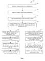
- FIG. 4is a cross sectional view of a magnetic storage element 100 with high magneto-resistance in a top spin valve configuration with seed and buffer layers on a NiFe substrate that are configured to support formation of one or more Heusler alloy layers in accordance with one embodiment of the invention.
- the magnetic storage element 100includes a multi-layer stacked structure with a bottom shield layer 102 , a substrate 104 on the bottom shield layer 102 , a seed layer 106 on the substrate 104 , a buffer layer 108 on the seed layer 106 , a free layer 110 on the buffer layer 108 , a spacer layer 112 on the free layer 110 , a sub-reference layer 114 on the spacer layer 112 , an interlayer coupling layer 116 on the sub-reference layer 114 , a pinned layer 118 on the interlayer coupling layer 116 , an anti-ferromagnetic (AFM) pinning layer 120 on the pinned layer 118 , a capping layer 122 on the AFM pinning layer 120 , and a top shield layer 124 on the capping layer 122 .
- AFManti-ferromagnetic
- the sub-reference layer 114 , the interlayer coupling layer 116 , and the pinned layer 118are collectively referred to as the reference layer.
- the AFM pinning layer 120is an optional layer.
- the bottom and top shield layers ( 102 , 124 )are made of suitable shield materials known in the art.
- the substrate 102is made of NiFe and other suitable materials.
- the seed layer 106can be made of a multi-layer structure that includes one or more materials such as NiFe, Ta, Ti, amorphous CoFeB, CoFe, a material including a magnetic CFMS Heusler alloy, and combinations thereof.
- the seed layer 106is made of a bottom NiFe layer that is about 2 nanometers (nm) thick, a CoFeB layer that is about 2 nm thick, and a CoFe layer that is about 4.5 nm thick.
- other suitable layers and thicknessescan be used.
- the buffer layer 108can be made of a multi-layer structure that includes one or more materials such as Ta, Ti, Cr, Ru, Cu, Ag, Al, W, a Ta alloy, a Cr alloy, a Ru alloy, a Cu alloy, a Ag alloy, a W alloy, a NiAl alloy, and combinations thereof.
- buffer layer 108is made of a bottom Cr layer that is about 1 nm thick and a Ag layer that is about 1 nm thick.
- the seed layer 106can be made of a bottom NiFe layer that is about 2 nanometers (nm) thick, a CoFeB layer that is about 2 nm thick, and a CoFe25 layer that is about 4.5 nm thick.
- the NiFe layer of the seed layer 106provides a contact layer for wafer substrate 104 for adhesion and stress adjustment.
- the CoFeBprovides an amorphous platform upon which the CoFe25 layer is grown to form a body-centered cubic (BCC) like structure.
- BCCbody-centered cubic
- the buffer layer 108 of Cr/Agis grown to provide (110) orientated texture and lattice match with Heusler alloy layers (e.g., free layer 110 ) that are to be grown epitaxially.
- the free layer 110can be a single or multi-layer structure made of one or more Heusler alloys grown epitaxially on the buffer layer 108 .
- the Heusler alloyscan have a L21/B2 ordering and/or include a Co 2 Fe x Mn 1-x Si or CFMS alloy, where x is between 0 and 1.
- the spacer layer 112can be made of suitable materials known in the art.
- the sub-reference layer 114can be a single or multi-layer structure made of Co, Fe, CoFe, and/or one or more Heusler alloys grown epitaxially on the spacer layer 112 .
- the Heusler alloyscan have a L21/B2 ordering and/or include a CFMS alloy.
- the interlayer coupling layer 116can be made of Ru, Cr, Cu, Ta, Ag, and/or other suitable materials known in the art.
- the pinned layer 118can be made of Co, Fe, CoFe, one or more Heusler alloys, and/or other suitable ferromagnetic materials.
- the AFM pinning layer 120can be made of anti-ferromagnetic materials such as IrMn, FeMn, PtMn, and/or other suitable materials known in the art.
- the capping layer 122can be made of Ru, Ta, Ti, and/or other suitable materials known in the art.
- the seed layer 106 and buffer layer 108are configured to facilitate an epitaxial growth of the Heusler alloy of the free layer 110 . More specifically, the seed layer 106 can be configured to substantially obstruct a transfer of a first crystalline structure of the substrate 104 to the buffer layer 108 and the free layer 110 , thereby preventing the transfer of the first crystalline structure to the Heusler alloy of the free layer 110 . In several embodiments, the seed layer 106 is configured to provide a second crystalline structure different from the first crystalline structure of the NiFe substrate 104 .
- the buffer layer 108is configured to substantially maintain the second crystalline structure of the seed layer 106 , and a crystalline structure of the free layer 110 (e.g., Heusler alloy) grown epitaxially on the buffer layer 106 should substantially match the second crystalline structure of the buffer layer 108 and the seed layer 106 .
- the first crystalline structurehas a face-centered cubic (FCC) structure
- the second crystalline structurehas a structure that is about body-centered cubic (BCC).
- the seed layer 106includes a first magnetic sub-layer with an amorphous structure and a second magnetic sub-layer with the second crystalline structure that is about body-centered cubic.
- the second crystalline structureis developed through a process for changing the amorphous structure of the first magnetic sub-layer, where the process is an annealing process, a phase change process, a re-crystallization process, a combination of those processes, and/or another suitable process known in the art.
- the seed layer 106 and the buffer layer 108are configured to provide a foundation structure for the Heusler alloy of the free layer 110 (e.g., upper layer) that is different from the first crystalline structure of the NiFe substrate 104 .
- the seed layer 106has substantially magnetic characteristics
- the buffer layer 108has substantially non-magnetic characteristics.
- the buffer layer 108includes one or more materials selected from the group consisting of Cu2CrAl, Cu2AlSi, a material including a non-magnetic Heusler alloy, and combinations thereof.
- the magnetic storage element 100is a current perpendicular to plane (CPP) giant magneto-resistance (GMR) reader.
- the substrate 104 and the seed layer 106can act as a shield layer for the GMR reader.
- one or both of shield layers ( 102 , 124 )are omitted.
- magnetic seed layers, buffer layers and their combined structureprovide a platform and base on which the Heusler alloy multi-layers and stacks are grown expitaxially to maximize the crystalline structure match and enhance L21/B2 ordering and stoichiometric homogeneity.
- the magnetic seed layerscan also act as part of the shielding and the use of which can be optional for MRAM applications but preferable for hard drive applications.
- the total Heusler alloy layersare less than 15 nm in thickness.
- the maximum CPP GMR ratiois about 9.0 and 13.0% for a device, corresponding to a maximum change in RA of about 4.5 and 7.0 m ⁇ m 2 , respectively. In one embodiment, the maximum CPP GMR of 13.0% and change in RA of about 9.0 m ⁇ m 2 are obtained for a CPP GMR device.
- the reference/pinned layershave multi-layer structures. They consist of two ferromagnetic layers anti-ferromagentically coupled by nonmagnetic coupling metal layers.
- the FM layersare made of Co, Fe, or Ni or their alloy or Heusler alloy layers.
- the interlayer coupling layerscan be nonmagnetic metals (their alloys) such as Ru, Cr, Cu, Ta, and Ag.
- An optional intermediate layercan be included as a thin interfacial layer of less than 20 Angstroms in thickness can be inserted in between the ferromagnetic and interlayer coupling layer.
- the intermediate layersare preferably made of magnetic metals or alloys that can enhance interlayer coupling and set forth texture and crystalline structures of the magnetic Heusler alloy layers and other magnetic layers.
- the epitaxial growth of the stacking layerse.g., Fe/Cr SAF pinned layers
- a resultant modulated crystalline structure with homogeneity in stoichiometry, of the device utilizing the Fe/Cr SAF pinned layersimproves homogeneity in the long-range ordering, and eventually the CPP GMR and device performance.
- the magnetic storage elementsprovide for large spin polarization and CPP GMR in magnetic elements utilizing Heusler systems, and the signal output on such devices is achieved with highly ordered L21/B2 Heusler phase using low temperature processes.
- the magnetic ordering temperatureis reduced for maximizing GMR and device performance for thin stack designs, while having scalability of device design to increase recording density.
- the magnetic storage elementsprovide for reduced shield-to-shield spacing (e.g., reduced by up to 10 nm as compared to conventional magnetic storage elements) and GMR gain up to two times conventional gain.
- the large output signal and amplitudeare available at low bias applied on the device, facilitating noise reduction including those from the spin transfer torque (STT) effect, and enhancement of SNR.
- the improved magnetic storage elementscan be used with MRAM device development and manufacturing in addition to hard drive applications.
- FIG. 5is a cross sectional view of a magnetic storage element 200 with high magneto-resistance in a bottom spin valve configuration with seed and buffer layers on a NiFe substrate that are configured to support formation of one or more Heusler alloy layers in accordance with one embodiment of the invention.
- the magnetic storage element 200includes a multi-layer stacked structure with a bottom shield layer 202 , a substrate 204 on the bottom shield layer 202 , a seed layer 206 on the substrate 204 , a buffer layer 208 on the seed layer 206 , an AFM pinning layer 220 on the buffer layer 208 , a pinned layer 218 on the AFM pinning layer 220 , an interlayer coupling layer 216 on the pinned layer 218 , a sub-reference layer 214 on the interlayer coupling layer 216 , a spacer layer 212 on the sub-reference layer 214 , a free layer 210 on the spacer layer 212 , a capping layer 222 on the free layer 210 , and a top shield layer 224 on the capping layer 222 .
- the sub-reference layer 214 , the interlayer coupling layer 216 , and the pinned layer 218are collectively referred to as the reference layer.
- the AFM pinning layer 220is an optional layer.
- the materials and function of the layers of the magnetic storage element 200can be the same, or substantially the same, as those described above for the magnetic storage element 100 of FIG. 4 .
- the magnetic storage element 200can also include the variations described above for the magnetic storage element 100 of FIG. 4 .
- FIG. 6is a cross sectional view of a magnetic storage element 300 with high magneto-resistance in a pseudo spin valve configuration with seed and buffer layers on a NiFe substrate that are configured to support formation of one or more Heusler alloy layers in accordance with one embodiment of the invention.
- the magnetic storage element 300includes a multi-layer stacked structure with a bottom shield layer 302 , a substrate 304 on the bottom shield layer 302 , a seed layer 306 on the substrate 304 , a buffer layer 308 on the seed layer 306 , a free layer 310 on the buffer layer 308 , a spacer layer 312 on the free layer 310 , a reference layer 315 on the spacer layer 312 , a capping layer 322 on the reference layer 315 , and a top shield layer 324 on the capping layer 322 .
- the materials and function of the layers of the magnetic storage element 300can be the same, or substantially the same, as those described above for the magnetic storage element 100 of FIG. 4 .
- the magnetic storage element 300can also include the variations described above for the magnetic storage element 100 of FIG. 4 .
- FIG. 7is a flowchart of a process 400 for forming a magnetic storage element with high magneto-resistance having seed and buffer layers on a NiFe substrate that are configured to support formation of one or more Heusler alloy layers in accordance with one embodiment of the invention.
- the process 400can be used to form one or more of the magnetic storage elements of FIGS. 4-6 .
- the processfirst deposits ( 402 ) a substrate including NiFe.
- the substratecan be deposited on a shield. In other embodiments, the substrate can act as a shield.
- the processdeposits ( 404 ) a seed layer on the substrate.
- the processdeposits ( 406 ) a buffer layer on the seed layer.
- the seed layer and buffer layerare configured to facilitate an epitaxial growth of a Heusler alloy about to be deposited.
- the processthen grows ( 408 ), epitaxially, an upper layer on the buffer layer where the upper layer includes a Heusler alloy.
- the upper layeris ( 410 ) to be a free layer to form a top spin valve or pseudo spin valve configuration for the magnetic storage element.
- the processdeposits ( 412 ) a spacer layer on the free layer.
- the processdeposits ( 414 ) a reference layer on the spacer layer where the reference layer includes a Heusler alloy.
- the reference layermay be a multi-layer structure.
- the processthen deposits ( 416 ) a capping layer on the reference layer.
- the upper layeris ( 418 ) to be a reference layer to form a bottom spin valve configuration magnetic storage element.
- the processdeposits ( 420 ) a spacer layer on the reference layer.
- the processdeposits ( 422 ) a free layer on the spacer layer where the free layer includes a Heusler alloy.
- the processthen deposits ( 424 ) a capping layer on the free layer.
- the processcan perform the sequence of actions in a different order. In another embodiment, the process can skip one or more of the actions. In other embodiments, one or more of the actions are performed simultaneously. In some embodiments, additional actions can be performed.
- the magnetic storage elementsinclude multi-layer stacked structures with the particular layers depicted in FIGS. 4-6 .
- additional layerscan be included or some of the layers may be omitted.
- the additional layersmay include one or more intervening layers positioned between the depicted layers.
- one or more layersmay be formed of a Heusler alloy grown epitaxially.
- the Heusler alloycan have be CFMS alloy and/or have a L21/B2 ordering.
Landscapes
- Engineering & Computer Science (AREA)
- Physics & Mathematics (AREA)
- Manufacturing & Machinery (AREA)
- Chemical & Material Sciences (AREA)
- Nanotechnology (AREA)
- Condensed Matter Physics & Semiconductors (AREA)
- General Physics & Mathematics (AREA)
- Mathematical Physics (AREA)
- Theoretical Computer Science (AREA)
- Crystallography & Structural Chemistry (AREA)
- Electromagnetism (AREA)
- Hall/Mr Elements (AREA)
Abstract
Description
Claims (13)
Priority Applications (2)
| Application Number | Priority Date | Filing Date | Title |
|---|---|---|---|
| US13/737,374US8760818B1 (en) | 2013-01-09 | 2013-01-09 | Systems and methods for providing magnetic storage elements with high magneto-resistance using heusler alloys |
| US14/290,961US9042057B1 (en) | 2013-01-09 | 2014-05-29 | Methods for providing magnetic storage elements with high magneto-resistance using Heusler alloys |
Applications Claiming Priority (1)
| Application Number | Priority Date | Filing Date | Title |
|---|---|---|---|
| US13/737,374US8760818B1 (en) | 2013-01-09 | 2013-01-09 | Systems and methods for providing magnetic storage elements with high magneto-resistance using heusler alloys |
Related Child Applications (1)
| Application Number | Title | Priority Date | Filing Date |
|---|---|---|---|
| US14/290,961DivisionUS9042057B1 (en) | 2013-01-09 | 2014-05-29 | Methods for providing magnetic storage elements with high magneto-resistance using Heusler alloys |
Publications (1)
| Publication Number | Publication Date |
|---|---|
| US8760818B1true US8760818B1 (en) | 2014-06-24 |
Family
ID=50944096
Family Applications (2)
| Application Number | Title | Priority Date | Filing Date |
|---|---|---|---|
| US13/737,374ActiveUS8760818B1 (en) | 2013-01-09 | 2013-01-09 | Systems and methods for providing magnetic storage elements with high magneto-resistance using heusler alloys |
| US14/290,961ActiveUS9042057B1 (en) | 2013-01-09 | 2014-05-29 | Methods for providing magnetic storage elements with high magneto-resistance using Heusler alloys |
Family Applications After (1)
| Application Number | Title | Priority Date | Filing Date |
|---|---|---|---|
| US14/290,961ActiveUS9042057B1 (en) | 2013-01-09 | 2014-05-29 | Methods for providing magnetic storage elements with high magneto-resistance using Heusler alloys |
Country Status (1)
| Country | Link |
|---|---|
| US (2) | US8760818B1 (en) |
Cited By (117)
| Publication number | Priority date | Publication date | Assignee | Title |
|---|---|---|---|---|
| US8917581B1 (en) | 2013-12-18 | 2014-12-23 | Western Digital Technologies, Inc. | Self-anneal process for a near field transducer and chimney in a hard disk drive assembly |
| US20150028439A1 (en)* | 2013-07-23 | 2015-01-29 | Micron Technology, Inc. | Memory cells, methods of fabrication, semiconductor device structures, memory systems, and electronic systems |
| US8947985B1 (en) | 2013-07-16 | 2015-02-03 | Western Digital (Fremont), Llc | Heat assisted magnetic recording transducers having a recessed pole |
| US8953422B1 (en) | 2014-06-10 | 2015-02-10 | Western Digital (Fremont), Llc | Near field transducer using dielectric waveguide core with fine ridge feature |
| US8958272B1 (en) | 2014-06-10 | 2015-02-17 | Western Digital (Fremont), Llc | Interfering near field transducer for energy assisted magnetic recording |
| US8971160B1 (en) | 2013-12-19 | 2015-03-03 | Western Digital (Fremont), Llc | Near field transducer with high refractive index pin for heat assisted magnetic recording |
| US8970988B1 (en) | 2013-12-31 | 2015-03-03 | Western Digital (Fremont), Llc | Electric gaps and method for making electric gaps for multiple sensor arrays |
| US8976635B1 (en) | 2014-06-10 | 2015-03-10 | Western Digital (Fremont), Llc | Near field transducer driven by a transverse electric waveguide for energy assisted magnetic recording |
| US8980109B1 (en) | 2012-12-11 | 2015-03-17 | Western Digital (Fremont), Llc | Method for providing a magnetic recording transducer using a combined main pole and side shield CMP for a wraparound shield scheme |
| US8988812B1 (en) | 2013-11-27 | 2015-03-24 | Western Digital (Fremont), Llc | Multi-sensor array configuration for a two-dimensional magnetic recording (TDMR) operation |
| US8984740B1 (en) | 2012-11-30 | 2015-03-24 | Western Digital (Fremont), Llc | Process for providing a magnetic recording transducer having a smooth magnetic seed layer |
| US8988825B1 (en) | 2014-02-28 | 2015-03-24 | Western Digital (Fremont, LLC | Method for fabricating a magnetic writer having half-side shields |
| US8993217B1 (en) | 2013-04-04 | 2015-03-31 | Western Digital (Fremont), Llc | Double exposure technique for high resolution disk imaging |
| US8995087B1 (en) | 2006-11-29 | 2015-03-31 | Western Digital (Fremont), Llc | Perpendicular magnetic recording write head having a wrap around shield |
| US9001467B1 (en) | 2014-03-05 | 2015-04-07 | Western Digital (Fremont), Llc | Method for fabricating side shields in a magnetic writer |
| US8997832B1 (en) | 2010-11-23 | 2015-04-07 | Western Digital (Fremont), Llc | Method of fabricating micrometer scale components |
| US9007719B1 (en) | 2013-10-23 | 2015-04-14 | Western Digital (Fremont), Llc | Systems and methods for using double mask techniques to achieve very small features |
| US9007725B1 (en) | 2014-10-07 | 2015-04-14 | Western Digital (Fremont), Llc | Sensor with positive coupling between dual ferromagnetic free layer laminates |
| US9007879B1 (en) | 2014-06-10 | 2015-04-14 | Western Digital (Fremont), Llc | Interfering near field transducer having a wide metal bar feature for energy assisted magnetic recording |
| US9013836B1 (en) | 2013-04-02 | 2015-04-21 | Western Digital (Fremont), Llc | Method and system for providing an antiferromagnetically coupled return pole |
| US9042051B2 (en) | 2013-08-15 | 2015-05-26 | Western Digital (Fremont), Llc | Gradient write gap for perpendicular magnetic recording writer |
| US9042052B1 (en) | 2014-06-23 | 2015-05-26 | Western Digital (Fremont), Llc | Magnetic writer having a partially shunted coil |
| US9042057B1 (en) | 2013-01-09 | 2015-05-26 | Western Digital (Fremont), Llc | Methods for providing magnetic storage elements with high magneto-resistance using Heusler alloys |
| US9042058B1 (en) | 2013-10-17 | 2015-05-26 | Western Digital Technologies, Inc. | Shield designed for middle shields in a multiple sensor array |
| US9053735B1 (en) | 2014-06-20 | 2015-06-09 | Western Digital (Fremont), Llc | Method for fabricating a magnetic writer using a full-film metal planarization |
| US9064507B1 (en) | 2009-07-31 | 2015-06-23 | Western Digital (Fremont), Llc | Magnetic etch-stop layer for magnetoresistive read heads |
| US9065043B1 (en) | 2012-06-29 | 2015-06-23 | Western Digital (Fremont), Llc | Tunnel magnetoresistance read head with narrow shield-to-shield spacing |
| US9082423B1 (en) | 2013-12-18 | 2015-07-14 | Western Digital (Fremont), Llc | Magnetic recording write transducer having an improved trailing surface profile |
| US9087527B1 (en) | 2014-10-28 | 2015-07-21 | Western Digital (Fremont), Llc | Apparatus and method for middle shield connection in magnetic recording transducers |
| US9087534B1 (en) | 2011-12-20 | 2015-07-21 | Western Digital (Fremont), Llc | Method and system for providing a read transducer having soft and hard magnetic bias structures |
| US9104107B1 (en) | 2013-04-03 | 2015-08-11 | Western Digital (Fremont), Llc | DUV photoresist process |
| US9111558B1 (en) | 2014-03-14 | 2015-08-18 | Western Digital (Fremont), Llc | System and method of diffractive focusing of light in a waveguide |
| US9111564B1 (en) | 2013-04-02 | 2015-08-18 | Western Digital (Fremont), Llc | Magnetic recording writer having a main pole with multiple flare angles |
| US9111550B1 (en) | 2014-12-04 | 2015-08-18 | Western Digital (Fremont), Llc | Write transducer having a magnetic buffer layer spaced between a side shield and a write pole by non-magnetic layers |
| US9123362B1 (en) | 2011-03-22 | 2015-09-01 | Western Digital (Fremont), Llc | Methods for assembling an electrically assisted magnetic recording (EAMR) head |
| US9123358B1 (en) | 2012-06-11 | 2015-09-01 | Western Digital (Fremont), Llc | Conformal high moment side shield seed layer for perpendicular magnetic recording writer |
| US9123374B1 (en) | 2015-02-12 | 2015-09-01 | Western Digital (Fremont), Llc | Heat assisted magnetic recording writer having an integrated polarization rotation plate |
| US9135930B1 (en) | 2014-03-06 | 2015-09-15 | Western Digital (Fremont), Llc | Method for fabricating a magnetic write pole using vacuum deposition |
| US9135937B1 (en) | 2014-05-09 | 2015-09-15 | Western Digital (Fremont), Llc | Current modulation on laser diode for energy assisted magnetic recording transducer |
| US9142233B1 (en) | 2014-02-28 | 2015-09-22 | Western Digital (Fremont), Llc | Heat assisted magnetic recording writer having a recessed pole |
| US9147404B1 (en) | 2015-03-31 | 2015-09-29 | Western Digital (Fremont), Llc | Method and system for providing a read transducer having a dual free layer |
| US9147408B1 (en) | 2013-12-19 | 2015-09-29 | Western Digital (Fremont), Llc | Heated AFM layer deposition and cooling process for TMR magnetic recording sensor with high pinning field |
| US9153255B1 (en) | 2014-03-05 | 2015-10-06 | Western Digital (Fremont), Llc | Method for fabricating a magnetic writer having an asymmetric gap and shields |
| US9183854B2 (en) | 2014-02-24 | 2015-11-10 | Western Digital (Fremont), Llc | Method to make interferometric taper waveguide for HAMR light delivery |
| US9190079B1 (en) | 2014-09-22 | 2015-11-17 | Western Digital (Fremont), Llc | Magnetic write pole having engineered radius of curvature and chisel angle profiles |
| US9190085B1 (en) | 2014-03-12 | 2015-11-17 | Western Digital (Fremont), Llc | Waveguide with reflective grating for localized energy intensity |
| US9202493B1 (en) | 2014-02-28 | 2015-12-01 | Western Digital (Fremont), Llc | Method of making an ultra-sharp tip mode converter for a HAMR head |
| US9202480B2 (en) | 2009-10-14 | 2015-12-01 | Western Digital (Fremont), LLC. | Double patterning hard mask for damascene perpendicular magnetic recording (PMR) writer |
| US9214165B1 (en) | 2014-12-18 | 2015-12-15 | Western Digital (Fremont), Llc | Magnetic writer having a gradient in saturation magnetization of the shields |
| US9214169B1 (en) | 2014-06-20 | 2015-12-15 | Western Digital (Fremont), Llc | Magnetic recording read transducer having a laminated free layer |
| US9213322B1 (en) | 2012-08-16 | 2015-12-15 | Western Digital (Fremont), Llc | Methods for providing run to run process control using a dynamic tuner |
| US9214172B2 (en) | 2013-10-23 | 2015-12-15 | Western Digital (Fremont), Llc | Method of manufacturing a magnetic read head |
| US9230565B1 (en) | 2014-06-24 | 2016-01-05 | Western Digital (Fremont), Llc | Magnetic shield for magnetic recording head |
| US9236560B1 (en) | 2014-12-08 | 2016-01-12 | Western Digital (Fremont), Llc | Spin transfer torque tunneling magnetoresistive device having a laminated free layer with perpendicular magnetic anisotropy |
| US9245562B1 (en) | 2015-03-30 | 2016-01-26 | Western Digital (Fremont), Llc | Magnetic recording writer with a composite main pole |
| US9245543B1 (en) | 2010-06-25 | 2016-01-26 | Western Digital (Fremont), Llc | Method for providing an energy assisted magnetic recording head having a laser integrally mounted to the slider |
| US9245545B1 (en) | 2013-04-12 | 2016-01-26 | Wester Digital (Fremont), Llc | Short yoke length coils for magnetic heads in disk drives |
| US9251813B1 (en) | 2009-04-19 | 2016-02-02 | Western Digital (Fremont), Llc | Method of making a magnetic recording head |
| US20160043301A1 (en)* | 2014-08-06 | 2016-02-11 | Samsung Electronics Co., Ltd. | Method and system for providing magnetic junctions including heusler multilayers |
| US9263071B1 (en) | 2015-03-31 | 2016-02-16 | Western Digital (Fremont), Llc | Flat NFT for heat assisted magnetic recording |
| US9269382B1 (en) | 2012-06-29 | 2016-02-23 | Western Digital (Fremont), Llc | Method and system for providing a read transducer having improved pinning of the pinned layer at higher recording densities |
| US9280990B1 (en) | 2013-12-11 | 2016-03-08 | Western Digital (Fremont), Llc | Method for fabricating a magnetic writer using multiple etches |
| US9286919B1 (en) | 2014-12-17 | 2016-03-15 | Western Digital (Fremont), Llc | Magnetic writer having a dual side gap |
| US9305583B1 (en) | 2014-02-18 | 2016-04-05 | Western Digital (Fremont), Llc | Method for fabricating a magnetic writer using multiple etches of damascene materials |
| US9312064B1 (en) | 2015-03-02 | 2016-04-12 | Western Digital (Fremont), Llc | Method to fabricate a magnetic head including ion milling of read gap using dual layer hard mask |
| US9318130B1 (en) | 2013-07-02 | 2016-04-19 | Western Digital (Fremont), Llc | Method to fabricate tunneling magnetic recording heads with extended pinned layer |
| US9336814B1 (en) | 2013-03-12 | 2016-05-10 | Western Digital (Fremont), Llc | Inverse tapered waveguide for use in a heat assisted magnetic recording head |
| US9343098B1 (en) | 2013-08-23 | 2016-05-17 | Western Digital (Fremont), Llc | Method for providing a heat assisted magnetic recording transducer having protective pads |
| US9343087B1 (en) | 2014-12-21 | 2016-05-17 | Western Digital (Fremont), Llc | Method for fabricating a magnetic writer having half shields |
| US9349392B1 (en) | 2012-05-24 | 2016-05-24 | Western Digital (Fremont), Llc | Methods for improving adhesion on dielectric substrates |
| US9349394B1 (en) | 2013-10-18 | 2016-05-24 | Western Digital (Fremont), Llc | Method for fabricating a magnetic writer having a gradient side gap |
| US9361914B1 (en) | 2014-06-18 | 2016-06-07 | Western Digital (Fremont), Llc | Magnetic sensor with thin capping layer |
| US9361913B1 (en) | 2013-06-03 | 2016-06-07 | Western Digital (Fremont), Llc | Recording read heads with a multi-layer AFM layer methods and apparatuses |
| US9368134B1 (en) | 2010-12-16 | 2016-06-14 | Western Digital (Fremont), Llc | Method and system for providing an antiferromagnetically coupled writer |
| US9384763B1 (en) | 2015-03-26 | 2016-07-05 | Western Digital (Fremont), Llc | Dual free layer magnetic reader having a rear bias structure including a soft bias layer |
| US9384765B1 (en) | 2015-09-24 | 2016-07-05 | Western Digital (Fremont), Llc | Method and system for providing a HAMR writer having improved optical efficiency |
| US9396742B1 (en) | 2012-11-30 | 2016-07-19 | Western Digital (Fremont), Llc | Magnetoresistive sensor for a magnetic storage system read head, and fabrication method thereof |
| US9396743B1 (en) | 2014-02-28 | 2016-07-19 | Western Digital (Fremont), Llc | Systems and methods for controlling soft bias thickness for tunnel magnetoresistance readers |
| US9406331B1 (en) | 2013-06-17 | 2016-08-02 | Western Digital (Fremont), Llc | Method for making ultra-narrow read sensor and read transducer device resulting therefrom |
| US9424866B1 (en) | 2015-09-24 | 2016-08-23 | Western Digital (Fremont), Llc | Heat assisted magnetic recording write apparatus having a dielectric gap |
| US9431032B1 (en) | 2013-08-14 | 2016-08-30 | Western Digital (Fremont), Llc | Electrical connection arrangement for a multiple sensor array usable in two-dimensional magnetic recording |
| US9431039B1 (en) | 2013-05-21 | 2016-08-30 | Western Digital (Fremont), Llc | Multiple sensor array usable in two-dimensional magnetic recording |
| US9431047B1 (en) | 2013-05-01 | 2016-08-30 | Western Digital (Fremont), Llc | Method for providing an improved AFM reader shield |
| US9431038B1 (en) | 2015-06-29 | 2016-08-30 | Western Digital (Fremont), Llc | Method for fabricating a magnetic write pole having an improved sidewall angle profile |
| US9431031B1 (en) | 2015-03-24 | 2016-08-30 | Western Digital (Fremont), Llc | System and method for magnetic transducers having multiple sensors and AFC shields |
| US9437251B1 (en) | 2014-12-22 | 2016-09-06 | Western Digital (Fremont), Llc | Apparatus and method having TDMR reader to reader shunts |
| US9443541B1 (en) | 2015-03-24 | 2016-09-13 | Western Digital (Fremont), Llc | Magnetic writer having a gradient in saturation magnetization of the shields and return pole |
| US9449625B1 (en) | 2014-12-24 | 2016-09-20 | Western Digital (Fremont), Llc | Heat assisted magnetic recording head having a plurality of diffusion barrier layers |
| US9449621B1 (en) | 2015-03-26 | 2016-09-20 | Western Digital (Fremont), Llc | Dual free layer magnetic reader having a rear bias structure having a high aspect ratio |
| US9472216B1 (en) | 2015-09-23 | 2016-10-18 | Western Digital (Fremont), Llc | Differential dual free layer magnetic reader |
| US9484051B1 (en) | 2015-11-09 | 2016-11-01 | The Provost, Fellows, Foundation Scholars and the other members of Board, of the College of the Holy and Undivided Trinity of Queen Elizabeth near Dublin | Method and system for reducing undesirable reflections in a HAMR write apparatus |
| US9508365B1 (en) | 2015-06-24 | 2016-11-29 | Western Digital (Fremont), LLC. | Magnetic reader having a crystal decoupling structure |
| US9508363B1 (en) | 2014-06-17 | 2016-11-29 | Western Digital (Fremont), Llc | Method for fabricating a magnetic write pole having a leading edge bevel |
| US9508372B1 (en) | 2015-06-03 | 2016-11-29 | Western Digital (Fremont), Llc | Shingle magnetic writer having a low sidewall angle pole |
| US9530443B1 (en) | 2015-06-25 | 2016-12-27 | Western Digital (Fremont), Llc | Method for fabricating a magnetic recording device having a high aspect ratio structure |
| US9564150B1 (en) | 2015-11-24 | 2017-02-07 | Western Digital (Fremont), Llc | Magnetic read apparatus having an improved read sensor isolation circuit |
| US9595273B1 (en) | 2015-09-30 | 2017-03-14 | Western Digital (Fremont), Llc | Shingle magnetic writer having nonconformal shields |
| US9646639B2 (en) | 2015-06-26 | 2017-05-09 | Western Digital (Fremont), Llc | Heat assisted magnetic recording writer having integrated polarization rotation waveguides |
| US9666214B1 (en) | 2015-09-23 | 2017-05-30 | Western Digital (Fremont), Llc | Free layer magnetic reader that may have a reduced shield-to-shield spacing |
| US9711202B2 (en)* | 2015-11-30 | 2017-07-18 | SK Hynix Inc. | Electronic device |
| US9721595B1 (en) | 2014-12-04 | 2017-08-01 | Western Digital (Fremont), Llc | Method for providing a storage device |
| US9740805B1 (en) | 2015-12-01 | 2017-08-22 | Western Digital (Fremont), Llc | Method and system for detecting hotspots for photolithographically-defined devices |
| US9741366B1 (en) | 2014-12-18 | 2017-08-22 | Western Digital (Fremont), Llc | Method for fabricating a magnetic writer having a gradient in saturation magnetization of the shields |
| US9754611B1 (en) | 2015-11-30 | 2017-09-05 | Western Digital (Fremont), Llc | Magnetic recording write apparatus having a stepped conformal trailing shield |
| US9767831B1 (en) | 2015-12-01 | 2017-09-19 | Western Digital (Fremont), Llc | Magnetic writer having convex trailing surface pole and conformal write gap |
| US9786301B1 (en) | 2014-12-02 | 2017-10-10 | Western Digital (Fremont), Llc | Apparatuses and methods for providing thin shields in a multiple sensor array |
| US9799351B1 (en) | 2015-11-30 | 2017-10-24 | Western Digital (Fremont), Llc | Short yoke length writer having assist coils |
| US9812155B1 (en) | 2015-11-23 | 2017-11-07 | Western Digital (Fremont), Llc | Method and system for fabricating high junction angle read sensors |
| US9842615B1 (en) | 2015-06-26 | 2017-12-12 | Western Digital (Fremont), Llc | Magnetic reader having a nonmagnetic insertion layer for the pinning layer |
| US9858951B1 (en) | 2015-12-01 | 2018-01-02 | Western Digital (Fremont), Llc | Method for providing a multilayer AFM layer in a read sensor |
| US9881638B1 (en) | 2014-12-17 | 2018-01-30 | Western Digital (Fremont), Llc | Method for providing a near-field transducer (NFT) for a heat assisted magnetic recording (HAMR) device |
| US9934811B1 (en) | 2014-03-07 | 2018-04-03 | Western Digital (Fremont), Llc | Methods for controlling stray fields of magnetic features using magneto-elastic anisotropy |
| US9953670B1 (en) | 2015-11-10 | 2018-04-24 | Western Digital (Fremont), Llc | Method and system for providing a HAMR writer including a multi-mode interference device |
| US10037770B1 (en) | 2015-11-12 | 2018-07-31 | Western Digital (Fremont), Llc | Method for providing a magnetic recording write apparatus having a seamless pole |
| US10074387B1 (en) | 2014-12-21 | 2018-09-11 | Western Digital (Fremont), Llc | Method and system for providing a read transducer having symmetric antiferromagnetically coupled shields |
| CN112993148A (en)* | 2019-12-17 | 2021-06-18 | Tdk株式会社 | Magnetoresistive effect element |
| US20210318394A1 (en)* | 2020-03-10 | 2021-10-14 | Tdk Corporation | Magnetoresistance effect element |
Families Citing this family (6)
| Publication number | Priority date | Publication date | Assignee | Title |
|---|---|---|---|---|
| US10566015B2 (en) | 2016-12-12 | 2020-02-18 | Western Digital Technologies, Inc. | Spin transfer torque (STT) device with template layer for heusler alloy magnetic layers |
| US10355204B2 (en) | 2017-03-07 | 2019-07-16 | International Business Machines Corporation | Selective growth of seed layer for magneto-resistive random access memory |
| US10867625B1 (en) | 2019-03-28 | 2020-12-15 | Western Digital Technologies, Inc | Spin transfer torque (STT) device with template layer for Heusler alloy magnetic layers |
| US11528038B2 (en) | 2020-11-06 | 2022-12-13 | Western Digital Technologies, Inc. | Content aware decoding using shared data statistics |
| US11925124B2 (en) | 2021-01-12 | 2024-03-05 | Samsung Electronics Co., Ltd. | Insertion layers for perpendicularly magnetized Heusler layers with reduced magnetic damping |
| US12106784B2 (en) | 2022-12-08 | 2024-10-01 | Western Digital Technologies, Inc. | Read sensor with ordered heusler alloy free layer and semiconductor barrier layer |
Citations (22)
| Publication number | Priority date | Publication date | Assignee | Title |
|---|---|---|---|---|
| US4828966A (en) | 1987-12-04 | 1989-05-09 | Digital Equipment Corporation | Method for producing hall effect sensor for magnetic recording head |
| US6375761B1 (en) | 1998-08-28 | 2002-04-23 | The Research Foundation Of State University Of New York | Magnetoresistive material with two metallic magnetic phases |
| US6707649B2 (en) | 2001-03-22 | 2004-03-16 | Alps Electric Co., Ltd. | Magnetic sensing element permitting decrease in effective element size while maintaining large optical element size |
| JP2004146480A (en) | 2002-10-23 | 2004-05-20 | Hitachi Ltd | Magnetoresistance effect element and magnetic head in which a Heusler magnetic layer and a body-centered cubic non-magnetic intermediate layer are stacked |
| US6828897B1 (en) | 1996-08-26 | 2004-12-07 | Western Digital (Fremont), Inc. | Methods and compositions for optimizing interfacial properties of magnetoresistive sensors |
| JP2005116703A (en) | 2003-10-06 | 2005-04-28 | Alps Electric Co Ltd | Magnetic detecting element |
| US20050266274A1 (en) | 2004-06-01 | 2005-12-01 | Alps Electric Co., Ltd. | Magnetic sensor using half-metal for pinned magnetic layer |
| US20060050444A1 (en) | 2004-09-03 | 2006-03-09 | Hideaki Fukuzawa | Magnetoresistive element, magnetic head, magnetic recording apparatus, and magnetic memory |
| US7042686B2 (en) | 2001-01-22 | 2006-05-09 | Matsushita Electric Industrial Co., Ltd. | Magnetoresistive element and method for producing the same |
| US7310208B2 (en)* | 2004-06-21 | 2007-12-18 | Alps Electric Co., Ltd. | Magnetoresistive sensor containing self-pinned layer containing a plurality of magnetic sublayers with magnetostriction-enhancing layer made of a nonmagnetic material |
| US7336453B2 (en) | 2003-10-06 | 2008-02-26 | Alps Electric Co., Ltd. | Magnetic sensing element including pinned layer and/or free layer composed of [110] crystal planes-oriented Heusler alloy |
| US7336451B2 (en) | 2002-01-24 | 2008-02-26 | Alps Electric Co., Ltd. | Magnetic sensing element containing half-metallic alloy |
| US20080239591A1 (en)* | 2007-03-30 | 2008-10-02 | Kabushiki Kaisha Toshiba | Magneto-resistance effect element, and method for manufacturing the same |
| US7466525B2 (en) | 2004-09-03 | 2008-12-16 | Tdk Corporation | Magnetic sensing element including laminated film composed of half-metal and NiFe alloy as free layer |
| US7480122B2 (en) | 2005-03-02 | 2009-01-20 | Tdk Corporation | Magnetic detecting device having free layer or pinned layer formed by lamination of magnetic alloy and Cu layer and method of manufacturing magnetic detecting device |
| US7554776B2 (en) | 2004-09-01 | 2009-06-30 | Tdk Corporation | CCP magnetic detecting element including a self-pinned CoFe layer |
| US7558028B2 (en) | 2005-11-16 | 2009-07-07 | Hitachi Global Storage Technologies Netherlands B.V. | Magnetic head with improved CPP sensor using Heusler alloys |
| US7602592B2 (en) | 2005-05-26 | 2009-10-13 | Kabushiki Kaisha Toshiba | Magnetoresistive element including connection layers with magnetization alignment angles therebetween of 30 to 60° between metallic magnetic layers |
| US7667933B2 (en) | 2005-03-31 | 2010-02-23 | Kabushiki Kaisha Toshiba | Magnetic oscillating device based on spin transfer torque and magnetic sensor using the same |
| US20100072529A1 (en) | 2008-09-25 | 2010-03-25 | Takao Marukame | Stack having heusler alloy, magnetoresistive element and spin transistor using the stack, and method of manufacturing the same |
| US7760473B2 (en) | 2006-02-24 | 2010-07-20 | Tdk Corporation | Magnetoresistance element employing Heusler alloy as magnetic layer |
| US20120182647A1 (en)* | 2009-07-31 | 2012-07-19 | Hiromi Fuke | Magnetoresistive element |
Family Cites Families (532)
| Publication number | Priority date | Publication date | Assignee | Title |
|---|---|---|---|---|
| US6078479A (en) | 1993-08-10 | 2000-06-20 | Read-Rite Corporation | Magnetic tape head with flux sensing element |
| US6219205B1 (en) | 1995-10-10 | 2001-04-17 | Read-Rite Corporation | High density giant magnetoresistive transducer with recessed sensor |
| US5801531A (en) | 1996-01-18 | 1998-09-01 | Read-Rite Corporation | Apparatus and method for testing magnetic heads using translational slides and a rotatable arm |
| JPH09235669A (en) | 1996-02-27 | 1997-09-09 | Read Rite S M I Kk | Oxide film forming method and electronic device |
| US5764451A (en) | 1996-03-28 | 1998-06-09 | Read-Rite Corporation | Multi-tapped coil having tapped segments casaded for amplification for improving signal-to-noise ratio |
| US5793550A (en) | 1996-04-23 | 1998-08-11 | Read-Rite Corporation | Magnetoresistive head using sense currents of opposite polarities |
| US6103073A (en) | 1996-07-15 | 2000-08-15 | Read-Rite Corporation | Magnetic thin film head zero throat pole tip definition |
| US6178150B1 (en) | 1996-07-30 | 2001-01-23 | Seagate Technology Inc. | Offset optics for use with optical heads |
| US6058094A (en) | 1996-07-30 | 2000-05-02 | Seagate Technology Inc. | Flying magneto-optical head with a steerable mirror |
| US6081499A (en) | 1997-05-05 | 2000-06-27 | Seagate Technology, Inc. | Magneto-optical data storage system having an optical-processing flying head |
| US6034938A (en) | 1996-07-30 | 2000-03-07 | Seagate Technology, Inc. | Data storage system having an optical processing flying head |
| US6307715B1 (en) | 1996-08-30 | 2001-10-23 | Read-Rite Corporation | Head suspension having reduced torsional vibration |
| JPH10143820A (en) | 1996-11-08 | 1998-05-29 | Read Rite S M I Kk | Inductive/mr composite type thin film magnetic head |
| JPH10188222A (en) | 1996-12-20 | 1998-07-21 | Read Rite S M I Kk | Combined thin-film magnetic head |
| US5758406A (en) | 1997-02-07 | 1998-06-02 | Read-Rite Corporation | Method for assembling and electrical testing of a magnetic head |
| US6173486B1 (en) | 1997-03-04 | 2001-01-16 | Read-Rite Corporation | Thin film magnetic head with self-aligned pole tips |
| US5859754A (en) | 1997-04-03 | 1999-01-12 | Read-Rite Corporation | Magnetoresistive transducer having a common magnetic bias using assertive and complementary signals |
| US6032353A (en) | 1997-05-15 | 2000-03-07 | Read-Rite Corporation | Magnetic head with low stack height and self-aligned pole tips |
| JPH113510A (en) | 1997-06-10 | 1999-01-06 | Read Rite S M I Kk | Composite thin film magnetic head |
| US6166891A (en) | 1997-06-30 | 2000-12-26 | Read-Rite Corporation | Magnetoresistive sensor for high temperature environment using iridium manganese |
| US5966800A (en) | 1997-07-28 | 1999-10-19 | Read-Rite Corporation | Method of making a magnetic head with aligned pole tips and pole layers formed of high magnetic moment material |
| US6775902B1 (en) | 1997-07-28 | 2004-08-17 | Western Digital (Fremont) Inc. | Method of making a magnetic head with aligned pole tips |
| US5966591A (en) | 1997-08-07 | 1999-10-12 | Read-Rite Corporation | Method and tool for handling micro-mechanical structures |
| US6073338A (en) | 1997-08-19 | 2000-06-13 | Read-Rite Corporation | Thin film read head with coplanar pole tips |
| US6188549B1 (en) | 1997-12-10 | 2001-02-13 | Read-Rite Corporation | Magnetoresistive read/write head with high-performance gap layers |
| US6275354B1 (en) | 1998-01-21 | 2001-08-14 | Read-Rite Corporation | Magnetic head with a toroidal coil encompassing only one yoke layer |
| US5996213A (en) | 1998-01-30 | 1999-12-07 | Read-Rite Corporation | Thin film MR head and method of making wherein pole trim takes place at the wafer level |
| US6108166A (en) | 1998-03-12 | 2000-08-22 | Read-Rite Corporation | Current-pinned spin valve sensor |
| US6043959A (en) | 1998-03-23 | 2000-03-28 | Read-Rite Corporation | Inductive write head formed with flat yoke and merged with magnetoresistive read transducer |
| US6136166A (en) | 1998-03-27 | 2000-10-24 | Read-Rite Corporation | Apparatus for producing a uniform magnetic field over a large surface area of a wafer |
| US6046885A (en) | 1998-04-03 | 2000-04-04 | Intri-Plex Technologies, Inc. | Base plate suspension assembly in a hard disk drive with step in flange |
| US6399179B1 (en) | 1998-04-03 | 2002-06-04 | Intri-Plex Technologies, Inc. | Base plate for suspension assembly in hard disk drive with stress isolation |
| US6137662A (en) | 1998-04-07 | 2000-10-24 | Read-Rite Corporation | Magnetoresistive sensor with pinned SAL |
| US6034851A (en) | 1998-04-07 | 2000-03-07 | Read-Rite Corporation | Shorting bar and test clip for protecting magnetic heads from damage caused by electrostatic discharge during manufacture |
| US6049650A (en) | 1998-04-17 | 2000-04-11 | Seagate Technology, Inc. | Structure for micro-machine optical tooling and method for making and using |
| US6055138A (en) | 1998-05-06 | 2000-04-25 | Read-Rite Corporation | Thin film pedestal pole tips write head having narrower lower pedestal pole tip |
| US6178066B1 (en) | 1998-05-27 | 2001-01-23 | Read-Rite Corporation | Method of fabricating an improved thin film device having a small element with well defined corners |
| JPH11354859A (en) | 1998-06-05 | 1999-12-24 | Read Rite Smi Kk | Magnetoresistive element and magnetic head |
| US6018441A (en) | 1998-06-08 | 2000-01-25 | Read-Rite Corporation | Disk drive pivot bearing and actuator arm assembly |
| JPH11354860A (en) | 1998-06-10 | 1999-12-24 | Read Rite Smi Kk | Spin valve magnetic conversion element and magnetic head |
| US6377535B1 (en) | 1998-07-06 | 2002-04-23 | Read-Rite Corporation | High numerical aperture optical focusing device having a conical incident facet and a parabolic reflector for use in data storage systems |
| US6130779A (en) | 1998-07-06 | 2000-10-10 | Read-Rite Corporation | Near field magneto-optical head made using wafer processing techniques |
| US6229782B1 (en) | 1998-07-06 | 2001-05-08 | Read-Rite Corporation | High numerical aperture optical focusing device for use in data storage systems |
| US6212153B1 (en) | 1998-07-06 | 2001-04-03 | Read-Rite Corporation | High NA solid catadioptric focusing device having a flat kinoform phase profile |
| US6175476B1 (en) | 1998-08-18 | 2001-01-16 | Read-Rite Corporation | Synthetic spin-valve device having high resistivity anti parallel coupling layer |
| US6445536B1 (en) | 1998-08-27 | 2002-09-03 | Read-Rite Corporation | Dielectric stencil-defined write head for MR, GMR, and spin valve high density recording heads |
| JP2000091667A (en) | 1998-09-09 | 2000-03-31 | Read Rite Smi Kk | Spin valve magnetoresistance sensor and thin-film magnetic head |
| US6181525B1 (en) | 1998-09-23 | 2001-01-30 | Read-Rite Corporation | Read/write head with a limited range of motion relative to a load beam |
| JP2000113437A (en) | 1998-10-08 | 2000-04-21 | Read Rite Smi Kk | Manufacturing method for magnetic head device, magnetic head device and intermediate product of magnetic head device |
| US6330136B1 (en) | 1998-10-14 | 2001-12-11 | Read-Rite Corporation | Magnetic read sensor with SDT tri-layer and method for making same |
| US6137661A (en) | 1998-10-19 | 2000-10-24 | Read-Rite Corporation | System for providing a magnetoresistive head having higher efficiency |
| US6252743B1 (en) | 1998-11-02 | 2001-06-26 | Read-Rite Corporation | Read/write positioning arm with interspaced amplifier chips |
| US6118638A (en) | 1998-11-02 | 2000-09-12 | Read-Rite Corporation | CPP magnetoresistive device and method for making same |
| US6333830B2 (en) | 1998-11-09 | 2001-12-25 | Read-Rite Corporation | Low resistance coil structure for high speed writer |
| US6198609B1 (en) | 1998-11-09 | 2001-03-06 | Read-Rite Corporation | CPP Magnetoresistive device with reduced edge effect and method for making same |
| JP2000149233A (en) | 1998-11-11 | 2000-05-30 | Read Rite Smi Kk | Magnetic head device and its manufacture |
| US6160684A (en) | 1998-11-12 | 2000-12-12 | Read-Rite Corporation | Head suspension having tabs and force isolation welds for gram load reduction during swaging |
| US6233116B1 (en) | 1998-11-13 | 2001-05-15 | Read-Rite Corporation | Thin film write head with improved laminated flux carrying structure and method of fabrication |
| US6452765B1 (en) | 1998-11-18 | 2002-09-17 | Read-Rite Corporation | CoNbTi as high resistivity SAL material for high-density MR |
| US6190764B1 (en) | 1998-11-23 | 2001-02-20 | Read-Rite Corporation | Inductive write head for magnetic data storage media |
| US6221218B1 (en) | 1998-11-23 | 2001-04-24 | Read-Rite Corporation | Method of forming an inductive write head for magnetic data storage media |
| JP2000163713A (en) | 1998-11-27 | 2000-06-16 | Read Rite Smi Kk | Forming method of upper magnetic pole layer of thin film magnetic head, forming method of fine block pattern of high aspect ratio on bottom of step on surface having steps, and thin film magnetic head |
| US6633464B2 (en) | 1998-12-09 | 2003-10-14 | Read-Rite Corporation | Synthetic antiferromagnetic pinned layer with Fe/FeSi/Fe system |
| US6025988A (en) | 1998-12-17 | 2000-02-15 | Read-Rite Corporation | Interconnect adapter and head suspension assembly |
| US6258468B1 (en) | 1998-12-22 | 2001-07-10 | Read-Rite Corporation | AMR read sensor structure and method with high magnetoresistive coefficient |
| US6204999B1 (en) | 1998-12-23 | 2001-03-20 | Read-Rite Corporation | Method and system for providing a write head having a conforming pole structure |
| US6462920B1 (en) | 1998-12-23 | 2002-10-08 | Read-Rite Corporation | Method and system for reducing MR head instability |
| US6222707B1 (en) | 1998-12-28 | 2001-04-24 | Read-Rite Corporation | Bottom or dual spin valve having a seed layer that results in an improved antiferromagnetic layer |
| US6215625B1 (en) | 1999-01-04 | 2001-04-10 | Read-Rite Corporation | Apparatus and method for adhesive bridge suspension attachment |
| US6185077B1 (en) | 1999-01-06 | 2001-02-06 | Read-Rite Corporation | Spin valve sensor with antiferromagnetic and magnetostatically coupled pinning structure |
| JP2000207714A (en) | 1999-01-13 | 2000-07-28 | Read Rite Smi Kk | Magneto resistance effect type thin film magnetic head and manufacture of the same |
| US6277505B1 (en) | 1999-01-21 | 2001-08-21 | Read-Rite Corporation | Read sensor with improved thermal stability and manufacturing method therefor |
| US6094803A (en) | 1999-01-21 | 2000-08-01 | Read-Rite Corporation | Wafer processing techniques for near field magneto-optical head |
| US6418000B1 (en) | 1999-01-21 | 2002-07-09 | Read-Rite Corporation | Dual, synthetic spin valve sensor using current pinning |
| JP2000222709A (en) | 1999-02-01 | 2000-08-11 | Read Rite Smi Kk | Spin valve magnetoresistance sensor and thin film magnetic head |
| US6351355B1 (en) | 1999-02-09 | 2002-02-26 | Read-Rite Corporation | Spin valve device with improved thermal stability |
| US6801411B1 (en) | 1999-02-10 | 2004-10-05 | Western Digital (Fremont), Inc. | Dual stripe spin valve sensor without antiferromagnetic pinning layer |
| US6629357B1 (en) | 1999-02-10 | 2003-10-07 | Read-Rite Smi Corp. | Method of magnetic head manufacture |
| US6178070B1 (en) | 1999-02-11 | 2001-01-23 | Read-Rite Corporation | Magnetic write head and method for making same |
| US6404706B1 (en) | 1999-02-12 | 2002-06-11 | Read-Rite Corporation | Laser mounting for a thermally assisted GMR head |
| US6016290A (en) | 1999-02-12 | 2000-01-18 | Read-Rite Corporation | Read/write head with shifted waveguide |
| JP2000251223A (en) | 1999-02-23 | 2000-09-14 | Read Rite Smi Kk | Spin valve magnetoresistance sensor and thin-film magnetic head |
| US6134089A (en) | 1999-03-11 | 2000-10-17 | Read-Rite Corporation | Current perpendicular to plane magnetoresistive device with low resistance lead |
| US6765756B1 (en) | 1999-03-12 | 2004-07-20 | Western Digital (Fremont), Inc. | Ultra-short yoke and ultra-low stack height writer and method of fabrication |
| US6691226B1 (en) | 1999-03-16 | 2004-02-10 | Western Digital Ventures, Inc. | Computer system with disk drive having private key validation means for enabling features |
| US6532823B1 (en) | 1999-03-18 | 2003-03-18 | Read-Rite Corporation | Insulator layers for magnetoresistive transducers |
| US6198608B1 (en) | 1999-03-18 | 2001-03-06 | Read-Rite Corporation | MR sensor with blunt contiguous junction and slow-milling-rate read gap |
| US6417998B1 (en) | 1999-03-23 | 2002-07-09 | Read-Rite Corporation | Ultra small advanced write transducer and method for making same |
| US6297955B1 (en) | 1999-03-31 | 2001-10-02 | Western Digital Ventures, Inc. | Host assembly for an integrated computer module |
| US6411522B1 (en) | 1999-04-01 | 2002-06-25 | Western Digital Ventures, Inc. | Integrated computer module with EMI shielding plate |
| US6201673B1 (en) | 1999-04-02 | 2001-03-13 | Read-Rite Corporation | System for biasing a synthetic free layer in a magnetoresistance sensor |
| US6445553B2 (en) | 1999-04-02 | 2002-09-03 | Read-Rite Corporation | Method and system for fabricating a high density magnetoresistive device |
| US6359779B1 (en) | 1999-04-05 | 2002-03-19 | Western Digital Ventures, Inc. | Integrated computer module with airflow accelerator |
| US6282056B1 (en) | 1999-04-08 | 2001-08-28 | Read-Rite Corporation | Tapered stitch pole writer for high density magnetic recording |
| US6490125B1 (en) | 1999-04-09 | 2002-12-03 | Read-Rite Corporation | Thin film write head with improved yoke to pole stitch |
| US6657816B1 (en) | 1999-04-09 | 2003-12-02 | Ronald A. Barr | Thin film inductive read/write head with a sloped pole |
| US6654195B1 (en) | 1999-04-27 | 2003-11-25 | Western Digital Ventures, Inc. | Disk drive having a register set for providing real time position variables to a host |
| US6944938B1 (en) | 1999-05-03 | 2005-09-20 | Western Digital (Fremont), Inc. | Method of forming a magnetoresistive device |
| US6829819B1 (en) | 1999-05-03 | 2004-12-14 | Western Digital (Fremont), Inc. | Method of forming a magnetoresistive device |
| US6424505B1 (en) | 1999-05-06 | 2002-07-23 | Read-Rite Corporation | Method and system for providing electrostatic discharge protection for flex-on suspension, trace-suspension assembly, or cable-on suspension |
| JP2000315302A (en) | 1999-05-06 | 2000-11-14 | Read Rite Smi Kk | Composite thin film magnetic head |
| US6271604B1 (en) | 1999-05-10 | 2001-08-07 | Western Digital Corporation | Integrated computer module having a data integrity latch |
| US6349014B1 (en) | 1999-05-14 | 2002-02-19 | Read-Rite Corporation | Magnetic read/write device with insulated coil layer recessed into pole |
| US6410170B1 (en) | 1999-05-20 | 2002-06-25 | Read-Rite Corporation | High resistivity FeXN sputtered films for magnetic storage devices and method of fabrication |
| US6296955B1 (en) | 1999-05-24 | 2001-10-02 | Read-Rite Corporation | High moment and high permeability transducer structures and formation |
| US6400526B2 (en) | 1999-05-26 | 2002-06-04 | Read-Rite Corporation | Advanced writer for chip-on-load beam |
| US6193584B1 (en) | 1999-05-27 | 2001-02-27 | Read-Rite Corporation | Apparatus and method of device stripe height control |
| US6466401B1 (en) | 1999-06-02 | 2002-10-15 | Read-Rite Corporation | Thin film write head with interlaced coil winding and method of fabrication |
| US6762910B1 (en) | 1999-06-03 | 2004-07-13 | Western Digital (Fremont), Inc. | Data storage and retrieval apparatus with thin film read head having inset extra gap insulation layer and method of fabrication |
| US6433970B1 (en) | 1999-06-07 | 2002-08-13 | Read-Rite Corporation | Structure and method for redeposition free thin film CPP read sensor fabrication |
| US6389499B1 (en) | 1999-06-09 | 2002-05-14 | Western Digital Ventures, Inc. | Integrated computer module |
| US6330137B1 (en) | 1999-06-11 | 2001-12-11 | Read-Rite Corporation | Magnetoresistive read sensor including a carbon barrier layer and method for making same |
| US6353511B1 (en) | 1999-06-15 | 2002-03-05 | Read-Rite Corporation | Thin film write head for improved high speed and high density recording |
| US6469877B1 (en) | 1999-06-15 | 2002-10-22 | Read-Rite Corporation | Spin valve device with improved exchange layer defined track width and method of fabrication |
| US6466402B1 (en) | 1999-06-18 | 2002-10-15 | Read-Rite Corporation | Compact MR write structure |
| US6185051B1 (en) | 1999-06-23 | 2001-02-06 | Read-Rite Corporation | High numerical aperture optical focusing device for use in data storage systems |
| US6310746B1 (en) | 1999-06-23 | 2001-10-30 | Read-Rite Corporation | Piezoelectric vibration damping for disk drives |
| US6181485B1 (en) | 1999-06-23 | 2001-01-30 | Read-Rite Corporation | High numerical aperture optical focusing device for use in data storage systems |
| US6185081B1 (en) | 1999-06-30 | 2001-02-06 | Read-Rite Corporation | Bias layers which are formed on underlayers promoting in-plane alignment of the c-axis of cobalt used in magnetoresistive transducers |
| US6687098B1 (en) | 1999-07-08 | 2004-02-03 | Western Digital (Fremont), Inc. | Top spin valve with improved seed layer |
| US7027268B1 (en) | 1999-07-08 | 2006-04-11 | Western Digital (Fremont), Inc. | Method and system for providing a dual spin filter |
| US6483662B1 (en) | 1999-07-09 | 2002-11-19 | Read-Rite Corporation | High density multi-coil magnetic write head having a reduced yoke length and short flux rise time |
| US7196880B1 (en) | 1999-07-19 | 2007-03-27 | Western Digital (Fremont), Inc. | Spin valve sensor having a nonmagnetic enhancement layer adjacent an ultra thin free layer |
| US6304414B1 (en) | 1999-07-20 | 2001-10-16 | Read-Rite Corporation | Thin film magnetic write head having an ultra-low stack height |
| US6611398B1 (en) | 1999-08-09 | 2003-08-26 | Quantum Corporation | Tape head with support bars |
| US6369983B1 (en) | 1999-08-13 | 2002-04-09 | Read-Rite Corporation | Write head having a dry-etchable antireflective intermediate layer |
| US6396660B1 (en) | 1999-08-23 | 2002-05-28 | Read-Rite Corporation | Magnetic write element having a thermally dissipative structure |
| US6381095B1 (en) | 1999-08-31 | 2002-04-30 | Read-Rite Corporation | High performance thin film magnetic write element having high Bsat poles and method for making same |
| US6317290B1 (en) | 1999-08-31 | 2001-11-13 | Read-Rite Corporation | Advance pole trim writer with moment P1 and low apex angle |
| US6452742B1 (en) | 1999-09-02 | 2002-09-17 | Read-Rite Corporation | Thin film write having reduced resistance conductor coil partially recessed within middle coat insulation |
| US6496330B1 (en) | 1999-09-09 | 2002-12-17 | Read-Rite Corporation | Magnetic write head having a splitcoil structure |
| US6421212B1 (en) | 1999-09-21 | 2002-07-16 | Read-Rite Corporation | Thin film read head structure with improved bias magnet-to-magnetoresistive element interface and method of fabrication |
| US6356412B1 (en) | 1999-09-30 | 2002-03-12 | Read-Rite Corporation | Air bearing facilitating load/unload of a magnetic read/write head |
| US6317297B1 (en) | 1999-10-06 | 2001-11-13 | Read-Rite Corporation | Current pinned dual spin valve with synthetic pinned layers |
| US6310750B1 (en) | 1999-10-20 | 2001-10-30 | Read-Rite Corporation | Disk drive actuator arm with microactuated read/write head positioning |
| US6381105B1 (en) | 1999-10-22 | 2002-04-30 | Read-Rite Corporation | Hybrid dual spin valve sensor and method for making same |
| JP2001126219A (en) | 1999-10-28 | 2001-05-11 | Read Rite Corp | Spin valve magneto-resistive sensor and thin film magnetic head |
| US6448765B1 (en) | 1999-10-28 | 2002-09-10 | Read-Rite Corporation | Microscopic tips having stable magnetic moments and disposed on cantilevers for sensing magnetic characteristics of adjacent structures |
| US6456465B1 (en) | 1999-11-09 | 2002-09-24 | Read-Rite Corporation | Vertical giant magnetoresistance sensor using a recessed shield |
| US6661621B1 (en) | 1999-11-19 | 2003-12-09 | Read-Rite Smi Corp. | Compound thin film magnetic head |
| US6447935B1 (en) | 1999-11-23 | 2002-09-10 | Read-Rite Corporation | Method and system for reducing assymetry in a spin valve having a synthetic pinned layer |
| US6479096B1 (en) | 1999-12-03 | 2002-11-12 | Read-Rite Corporation | Method for manufacturing a GMR spin valve having a smooth interface between magnetic and non-magnetic layers |
| US6650506B1 (en) | 1999-12-15 | 2003-11-18 | Patrick Risse | Double-sided disk storage using a single configuration of magnetoresistive head |
| US6437945B1 (en) | 1999-12-28 | 2002-08-20 | Read-Rite Corporation | Airflow assisted ramp loading and unloading of sliders in hard disk drives |
| US7046490B1 (en) | 2000-01-06 | 2006-05-16 | Western Digital (Fremont), Inc. | Spin valve magnetoresistance sensor and thin film magnetic head |
| US6404601B1 (en) | 2000-01-25 | 2002-06-11 | Read-Rite Corporation | Merged write head with magnetically isolated poletip |
| US6417999B1 (en) | 2000-02-04 | 2002-07-09 | Read-Rite Corporation | Magnetoresistive head stabilized structure and method of fabrication thereof |
| US7023658B1 (en) | 2000-02-08 | 2006-04-04 | Western Digital (Fremont), Inc. | Submicron track-width pole-tips for electromagnetic transducers |
| US6721149B1 (en) | 2000-02-11 | 2004-04-13 | Western Digital (Fremont), Inc. | Tunneling magnetoresistance spin-valve read sensor with LaNiO3 spacer |
| US6724569B1 (en) | 2000-02-16 | 2004-04-20 | Western Digital (Fremont), Inc. | Thin film writer with multiplayer write gap |
| US6433965B1 (en) | 2000-03-02 | 2002-08-13 | Read-Rite Corporation | Laminated carbon-containing overcoats for information storage system transducers |
| US6445542B1 (en) | 2000-03-06 | 2002-09-03 | Read-Rite Corporation | Air bearing slider |
| US7059868B1 (en) | 2000-03-07 | 2006-06-13 | Western Digital (Fremont), Inc. | Connection of trace circuitry in a computer disk drive system |
| US6353318B1 (en) | 2000-03-10 | 2002-03-05 | Read-Rite Corporation | Magnetoresistive sensor having hard biased current perpendicular to the plane sensor |
| US6445554B1 (en) | 2000-03-10 | 2002-09-03 | Read-Rite Corporation | Method and system for providing edge-junction TMR for high areal density magnetic recording |
| JP2001308411A (en) | 2000-04-11 | 2001-11-02 | Read Rite Corp | Spin bubble type magnetoresistance sensor and thin film magnetic head |
| US6433968B1 (en) | 2000-05-02 | 2002-08-13 | Read-Rite Corporation | Merged read/write head and method of fabricating same |
| US6552874B1 (en) | 2000-05-17 | 2003-04-22 | Read-Rite Corporation | Shared pole magnetic read-write head for achieving optimized erase band width and method of fabricating the same |
| US6496334B1 (en) | 2000-05-26 | 2002-12-17 | Read-Rite Corportion | Data storage and retrieval apparatus with thin film read head having planarized extra gap and shield layers and method of fabrication thereof |
| US6700759B1 (en) | 2000-06-02 | 2004-03-02 | Western Digital (Fremont), Inc. | Narrow track width magnetoresistive sensor and method of making |
| US6674610B1 (en) | 2000-06-16 | 2004-01-06 | Western Digital (Fremont), Inc. | Thin film write head with universal coil design |
| US6515573B1 (en) | 2000-06-19 | 2003-02-04 | Read-Rite Corporation | Method and system for providing edge-junction TMR utilizing a hard magnet as a pinned layer |
| US6430806B1 (en) | 2000-06-23 | 2002-08-13 | Read-Rite Corporation | Method for manufacturing an inductive write element employing bi-layer photoresist to define a thin high moment pole pedestal |
| US6512657B2 (en) | 2000-07-17 | 2003-01-28 | Read-Rite Corporation | Head suspension having gram load change reduction and method of assembly |
| US6618223B1 (en) | 2000-07-18 | 2003-09-09 | Read-Rite Corporation | High speed, high areal density inductive writer |
| US6512661B1 (en) | 2000-08-10 | 2003-01-28 | Read-Rite Corporation | Vertical giant magnetoresistance sensor utilizing an insulating bias layer |
| US6859997B1 (en) | 2000-09-19 | 2005-03-01 | Western Digital (Fremont), Inc. | Method for manufacturing a magnetic write element |
| US6989962B1 (en) | 2000-09-26 | 2006-01-24 | Western Digital (Fremont), Inc. | Inductive write head having high magnetic moment poles and low magnetic moment thin layer in the back gap, and methods for making |
| US6801408B1 (en) | 2000-11-02 | 2004-10-05 | Western Digital (Fremont), Inc. | Data storage and retrieval apparatus with thin film read head having a planar sensor element and an extra gap and method of fabrication thereof |
| US6807332B1 (en) | 2000-11-06 | 2004-10-19 | Western Digital (Fremont), Inc. | Piezoelectric actuated optical switch |
| US6958885B1 (en) | 2000-12-21 | 2005-10-25 | Western Digital (Fremont), Inc. | Insulation layer structure for inductive write heads and method of fabrication |
| US6785955B1 (en) | 2001-01-23 | 2004-09-07 | Western Digital (Fremont), Inc. | Method for providing pedestal-defined zero throat writer |
| US6577470B1 (en) | 2001-01-25 | 2003-06-10 | Read-Rite Corporation | Method and system for providing a tape head subassembly structure having an integrated wear bar and outrigger rail |
| US6661625B1 (en) | 2001-02-20 | 2003-12-09 | Kyusik Sin | Spin-dependent tunneling sensor with low resistance metal oxide tunnel barrier |
| US6888184B1 (en) | 2001-02-23 | 2005-05-03 | Western Digital (Fremont), Inc. | Shielded magnetic ram cells |
| US6552928B1 (en) | 2001-02-23 | 2003-04-22 | Read-Rite Corporation | Read-write control circuit for magnetic tunnel junction MRAM |
| US6687178B1 (en) | 2001-02-23 | 2004-02-03 | Western Digital (Fremont), Inc. | Temperature dependent write current source for magnetic tunnel junction MRAM |
| US6721203B1 (en) | 2001-02-23 | 2004-04-13 | Western Digital (Fremont), Inc. | Designs of reference cells for magnetic tunnel junction (MTJ) MRAM |
| US6803615B1 (en) | 2001-02-23 | 2004-10-12 | Western Digital (Fremont), Inc. | Magnetic tunnel junction MRAM with improved stability |
| US6873547B1 (en) | 2001-02-23 | 2005-03-29 | Read Rite Corporation | High capacity MRAM memory array architecture |
| US6700738B1 (en) | 2001-03-16 | 2004-03-02 | Kyusik Sin | Read/write head coil tap having upper and lower portions |
| US7289303B1 (en) | 2001-04-05 | 2007-10-30 | Western Digital (Fremont), Llc | Spin valve sensors having synthetic antiferromagnet for longitudinal bias |
| US6515791B1 (en) | 2001-04-06 | 2003-02-04 | Read-Rite Corporation | Active reflection and anti-reflection optical switch |
| US6829160B1 (en) | 2001-04-06 | 2004-12-07 | Western Digital (Fremont), Inc. | Magnetic ram cell with amplification circuitry and MRAM memory array formed using the MRAM cells |
| US6704158B2 (en) | 2001-06-05 | 2004-03-09 | Western Digital (Fremont), Inc. | Shear mode multilayered collocated micro-actuator for dual-stage servo controllers in disk drives |
| US6376964B1 (en) | 2001-05-16 | 2002-04-23 | Read-Rite Corporation | Collocated rotating flexure microactuator for dual-stage servo in disk drives |
| US6760196B1 (en) | 2001-12-12 | 2004-07-06 | Western Digital, Inc. | Microactuator with offsetting hinges and method for high-resolution positioning of magnetic read/write head |
| US6870712B2 (en) | 2001-06-05 | 2005-03-22 | Western Digital (Fremont), Inc. | Inductive writer with flat top pole and pedestal defined zero throat |
| US6798616B1 (en) | 2001-07-10 | 2004-09-28 | Western Digital (Fremont), Inc. | Write head architecture for improved manufacturability |
| US7349179B1 (en) | 2001-07-16 | 2008-03-25 | Western Digital (Fremont), Llc | Write head for improved manufacturability larger write field and reduced adjacent track erasure |
| US6683763B1 (en) | 2001-08-15 | 2004-01-27 | Western Digital (Fremont), Inc. | Method and system for providing a self-aligned electrical contact for a TMR element |
| US6512690B1 (en) | 2001-08-15 | 2003-01-28 | Read-Rite Corporation | High sensitivity common source amplifier MRAM cell, memory array and read/write scheme |
| US6418048B1 (en) | 2001-08-15 | 2002-07-09 | Read-Rite Corporation | Spin-dependent tunneling sensor suitable for a magnetic memory |
| US6809899B1 (en) | 2001-08-20 | 2004-10-26 | Western Digital (Fremont), Inc. | Magnetic heads for perpendicular recording with trapezoidal pole tips |
| US7027274B1 (en) | 2001-08-30 | 2006-04-11 | Western Digital (Fremont), Inc. | Spin-dependent tunneling read/write sensor for hard disk drives |
| US6791793B1 (en) | 2001-09-14 | 2004-09-14 | Western Digital (Fremont), Inc. | Perpendicular recording write head having a recessed magnetic adjunct pole and method of making the same |
| US6816345B1 (en) | 2001-09-24 | 2004-11-09 | Western Digital (Fremont), Inc. | Magnetoresistive sensors having submicron track widths and method of making |
| US6754049B1 (en) | 2001-10-16 | 2004-06-22 | Western Digital (Fremont), Inc. | Transducers for perpendicular recording with inductive cancellation at MR sensor |
| US6987643B1 (en) | 2001-10-23 | 2006-01-17 | Western Digital (Fremont), Inc. | Pole structure to relieve adjacent track writing |
| US6721138B1 (en) | 2001-10-24 | 2004-04-13 | Western Digital (Fremont), Inc. | Inductive transducer with stitched pole tip and pedestal defining zero throat height |
| US7054113B1 (en) | 2001-10-25 | 2006-05-30 | Western Digital (Fremont), Inc. | Reader/writer for magnetic memory |
| US6583968B1 (en) | 2001-10-31 | 2003-06-24 | Western Digital Technologies, Inc. | Spindle motor hub having equivalent MR read element bias voltage to mitigate potential between disk and MR read element |
| US6807030B1 (en) | 2001-12-18 | 2004-10-19 | Western Digital (Fremont), Inc. | Enclosed piezoelectric microactuators coupled between head and suspension |
| US6961221B1 (en) | 2001-12-18 | 2005-11-01 | Western Digital (Fremont), Inc. | Piezoelectric microactuators with substantially fixed axis of rotation and magnified stroke |
| US6737281B1 (en) | 2002-01-08 | 2004-05-18 | Western Digital (Fremont), Inc. | Method of making transducer with inorganic nonferromagnetic apex region |
| US6751055B1 (en) | 2002-01-08 | 2004-06-15 | Western Digital (Fremont), Inc. | Inductive transducer with reduced pole tip protrusion |
| US6747301B1 (en) | 2002-02-06 | 2004-06-08 | Western Digital (Fremont), Inc. | Spin dependent tunneling barriers formed with a magnetic alloy |
| US6639291B1 (en) | 2002-02-06 | 2003-10-28 | Western Digital (Fremont), Inc. | Spin dependent tunneling barriers doped with magnetic particles |
| US6724572B1 (en) | 2002-02-28 | 2004-04-20 | Western Digital, Inc. | Inductive transducer with recessed leading pole layer |
| US7307814B1 (en) | 2002-03-01 | 2007-12-11 | Western Digital (Fremont), Llc | Pedestal defined zero throat writer having a recessed pedestal |
| US6859343B1 (en) | 2002-03-19 | 2005-02-22 | Western Digital, Inc. | Hybrid diffuser for minimizing thermal pole tip protrusion and reader sensor temperature |
| US7035046B1 (en) | 2002-03-19 | 2006-04-25 | Western Digital (Fremont), Inc. | System and method for minimizing thermal pole tip protrusion |
| US6757140B1 (en) | 2002-03-19 | 2004-06-29 | Western Digital, Inc. | Electrostatic microelectromechanical (MEM) microactuator for precise read/write head positioning |
| US6873494B2 (en) | 2002-04-29 | 2005-03-29 | Western Digital (Fremont), Inc. | Write head with high moment film layer having tapered portion extending beyond write gap layer |
| US7522377B1 (en) | 2002-05-01 | 2009-04-21 | Western Digital (Fremont), Llc | Magnetic write head with high moment magnetic thin film formed over seed layer |
| US6778358B1 (en) | 2002-05-01 | 2004-08-17 | Western Digital (Fremont), Inc. | Magnetically soft, high saturation magnetization laminates of iron-cobalt-nitrogen and iron-nickel |
| US6744608B1 (en) | 2002-05-14 | 2004-06-01 | Western Digital (Fremont), Inc. | Method and system for making TMR junctions |
| US6942824B1 (en) | 2002-05-22 | 2005-09-13 | Western Digital (Fremont), Inc. | UV curable and electrically conductive adhesive for bonding magnetic disk drive components |
| US6909578B1 (en) | 2002-05-30 | 2005-06-21 | Western Digital (Fremont), Inc. | Method and system for reducing thermal pole tip protrusion |
| US7133253B1 (en) | 2002-06-03 | 2006-11-07 | Western Digital (Fremont), Inc. | Pole tip with sides flared at media-facing surface |
| US6806035B1 (en) | 2002-06-25 | 2004-10-19 | Western Digital (Fremont), Inc. | Wafer serialization manufacturing process for read/write heads using photolithography and selective reactive ion etching |
| US6861937B1 (en) | 2002-06-25 | 2005-03-01 | Western Digital (Fremont), Inc. | Double winding twin coil for thin-film head writer |
| US6680863B1 (en) | 2002-07-09 | 2004-01-20 | Western Digital (Fremont), Inc. | MRAM memory array having merged word lines |
| US6707083B1 (en) | 2002-07-09 | 2004-03-16 | Western Digital (Fremont), Inc. | Magnetic tunneling junction with improved power consumption |
| US6713801B1 (en) | 2002-07-09 | 2004-03-30 | Western Digital (Fremont), Inc. | α-tantalum lead for use with magnetic tunneling junctions |
| US6975486B2 (en) | 2002-08-06 | 2005-12-13 | Western Digital (Fremont), Inc. | Thin film write head having a laminated, flat top pole with bottom shaper and method of fabrication |
| US6912106B1 (en) | 2002-08-06 | 2005-06-28 | Western Digital (Fremont), Inc. | Writer with a hot seed zero throat and substantially flat top pole |
| US6894871B2 (en) | 2002-08-07 | 2005-05-17 | Western Digital (Fremont), Inc. | Technique for reducing pole tip protrusion in a magnetic write head and GMR stripe temperature in an associated read head structure utilizing one or more internal diffuser regions |
| US6879464B2 (en) | 2002-08-16 | 2005-04-12 | Western Digital (Fremont), Inc. | Air bearing having a cavity patch surface coplanar with a leading edge pad surface |
| US7211339B1 (en) | 2002-08-22 | 2007-05-01 | Western Digital (Fremont), Inc. | Highly conductive lead adjoining MR stripe and extending beyond stripe height at junction |
| US6989972B1 (en) | 2002-09-30 | 2006-01-24 | Western Digital (Fremont), Inc. | Magnetoresistive sensor with overlapping leads having distributed current |
| US6934129B1 (en) | 2002-09-30 | 2005-08-23 | Western Digital (Fremont), Inc. | Magnetoresistive sensor with overlapping lead layers including alpha tantalum and conductive layers |
| US6940688B2 (en) | 2002-10-21 | 2005-09-06 | Western Digital (Fremont), Inc. | Coil inductive writer having a low inductance and short yoke length |
| US6950266B1 (en) | 2002-10-28 | 2005-09-27 | Western Digital (Fremont), Inc. | Active fly height control crown actuator |
| US6891702B1 (en) | 2002-10-31 | 2005-05-10 | Western Digital Technologies, Inc. | Method and devices for providing magnetoresistive heads with protection from electrostatic discharge and electric overstress events |
| US7113366B1 (en) | 2002-11-07 | 2006-09-26 | Western Digital (Fremont), Inc. | Double-nosed inductive transducer with reduced off-track writing |
| US7116517B1 (en) | 2002-12-18 | 2006-10-03 | Western Digital (Fremont), Inc. | Stitched pole write element with a T-shaped pole tip portion |
| US7057857B1 (en) | 2002-12-20 | 2006-06-06 | Western Digital (Fremont), Inc. | Dimple pivot post for a rotary co-located microactuator |
| US6888704B1 (en) | 2003-01-22 | 2005-05-03 | Western Digital (Fremont), Inc. | Method and system for providing high sensitivity giant magnetoresistive sensors |
| US6943993B2 (en) | 2003-02-11 | 2005-09-13 | Western Digital (Fremont), Inc. | Magnetic recording head with a side shield structure for controlling side reading of thin film read sensor |
| US7006327B2 (en) | 2003-02-27 | 2006-02-28 | Western Digital (Fremont), Inc. | Thin film recording head with a buried coil providing a shortened yoke and improved dimension control |
| US7286329B1 (en) | 2003-04-02 | 2007-10-23 | Western Digital (Fremont), Llc | GMR sensor with shallow contiguous junction and bias layers aligned with free sensor layers |
| US7012832B1 (en) | 2003-10-31 | 2006-03-14 | Western Digital (Fremont), Inc. | Magnetic memory cell with plural read transistors |
| US7126788B1 (en) | 2003-11-26 | 2006-10-24 | Western Digital (Fremont), Inc. | Trailing edge recording magnetic head with reversed double bias coil and deflection pole for perpendicular recording with a non-perpendicular write field |
| US7126790B1 (en) | 2003-11-26 | 2006-10-24 | Western Digital (Fremont), Inc. | Magnetic head for perpendicular recording with magnetic loop providing non-perpendicular write field |
| US7310204B1 (en) | 2003-12-19 | 2007-12-18 | Western Digital (Fremont), Llc | Inductive writer design for using a soft magnetic pedestal having a high magnetic saturation layer |
| US8104166B1 (en) | 2003-12-19 | 2012-01-31 | Western Digital (Fremont), Llc | Self-aligned method for fabricating a high density GMR read element |
| US7342752B1 (en) | 2004-01-31 | 2008-03-11 | Western Digital (Fremont), Llc | Magnetoresistive read head having a bias structure with at least one dusting layer |
| US7239478B1 (en) | 2004-01-31 | 2007-07-03 | Western Digital (Fremont), Inc. | Write element for perpendicular recording in a data storage system |
| US7199974B1 (en) | 2004-02-02 | 2007-04-03 | Western Digital (Fremont), Inc. | Read/write head with reduced pole tip protrusion |
| US7248433B1 (en) | 2004-02-02 | 2007-07-24 | Western Digital (Fremont), Inc. | Magnetic head with stitched top pole layer and single layer coil or solenoidal coil |
| US7292409B1 (en) | 2004-02-27 | 2007-11-06 | Western Digital (Fremont), Llc | Magnetic head with thin trailing pedestal layer |
| US7212384B1 (en) | 2004-02-27 | 2007-05-01 | Western Digital (Fremont), Inc. | Magnetic read head with recessed hard bias and current leads |
| US7639457B1 (en) | 2004-02-27 | 2009-12-29 | Western Digital (Fremont), Llc | Magnetic sensor with underlayers promoting high-coercivity, in-plane bias layers |
| US7333295B1 (en) | 2004-03-31 | 2008-02-19 | Western Digital (Fremont), Llc | Magnetic recording head with high saturation magnetic flux density CoNiFe thin film composition |
| US7280325B1 (en) | 2004-03-31 | 2007-10-09 | Western Digital (Fremont), Llc | Ferromagnetic structure including a first section separated from a ferromagnetic layer by an electrically conductive nonmagnetic spacer and a second section elongated relative to the first section in at least one dimension |
| US7248449B1 (en) | 2004-03-31 | 2007-07-24 | Western Digital (Fremont), Inc. | Magnetoresistive read sensor with reduced effective shield-to-shield spacing |
| US6934113B1 (en) | 2004-03-31 | 2005-08-23 | Western Digital (Fremont), Inc. | Method and system for providing dynamic actuation of a write head using a strain element |
| US8670211B1 (en) | 2004-03-31 | 2014-03-11 | Western Digital (Fremont), Llc | Method and system for providing high magnetic flux saturation CoFe films |
| US7110289B1 (en) | 2004-03-31 | 2006-09-19 | Western Digital (Fremont), Inc. | Method and system for controlling MRAM write current to reduce power consumption |
| US7193815B1 (en) | 2004-04-06 | 2007-03-20 | Western Digital (Fremont), Inc. | Shielded pole magnetic head for perpendicular recording |
| US7672086B1 (en) | 2004-04-28 | 2010-03-02 | Western Digital (Fremont), Llc | Method and system for providing a magnetic element having a current confined layer |
| US7660080B1 (en) | 2004-04-30 | 2010-02-09 | Western Digital (Fremont), Llc | Read/write head with dynamic flying height control by magnetostriction |
| US7248431B1 (en) | 2004-04-30 | 2007-07-24 | Yinshi Liu | Method of fabricating a perpendicular recording write head having a gap with two portions |
| US7307818B1 (en) | 2004-04-30 | 2007-12-11 | Western Digital (Fremont), Llc | Method and system for providing a stable spin filter |
| US7199975B1 (en) | 2004-05-15 | 2007-04-03 | Western Digital (Fremont), Inc. | Magnetic head for perpendicular recording with hard bias structure for write pole tip |
| US7092195B1 (en) | 2004-05-28 | 2006-08-15 | Western Digital (Fremont), Inc. | Method of using a magnetic write head having an internal heater |
| US7522379B1 (en) | 2004-07-30 | 2009-04-21 | Western Digital (Fremont), Llc | Write element with recessed pole and heat sink layer for ultra-high density writing |
| US7238292B1 (en) | 2004-07-30 | 2007-07-03 | Western Digital (Fremont), Inc. | Method of fabricating a write element with a reduced yoke length |
| US7379269B1 (en) | 2004-07-30 | 2008-05-27 | Western Digital (Fremont), Llc | Write element with reduced yoke length for ultra-high density writing |
| US7318947B1 (en) | 2004-08-31 | 2008-01-15 | Western Digital (Fremont), Llc | Method and apparatus for controlling magnetostriction in a spin valve sensor |
| US7170725B1 (en) | 2004-09-01 | 2007-01-30 | Western Digital (Fremont), Inc. | Magnetic sensor having an aluminum-nitride seed layer for an anti-ferromagnetic layer |
| US7595967B1 (en) | 2004-09-07 | 2009-09-29 | Western Digital (Fremont), Llp | Method for fabricating a spacer layer for a magnetoresistive element |
| US7296339B1 (en) | 2004-09-08 | 2007-11-20 | Western Digital (Fremont), Llc | Method for manufacturing a perpendicular magnetic recording head |
| US7124654B1 (en) | 2004-09-30 | 2006-10-24 | Western Digital (Fremont), Inc. | Method for determining a microactuator range of movement |
| US7131346B1 (en) | 2004-10-15 | 2006-11-07 | Western Digital (Fremont), Inc. | Spin stand testing system with fine positioner for head stack assembly |
| US7041985B1 (en) | 2004-11-12 | 2006-05-09 | Western Digital (Fremont), Inc. | Manipulator for microscopy sample preparation and methods for making and use thereof |
| US7284316B1 (en) | 2004-11-17 | 2007-10-23 | Western Digital (Fremont), Llc | Method for forming a hard bias structure in a magnetoresistive sensor |
| US7428124B1 (en) | 2005-01-18 | 2008-09-23 | Western Digital (Fremont), Llc | Magnetic recording head with resistive heating element and thermal barrier layer |
| US7430098B1 (en) | 2005-01-18 | 2008-09-30 | Western Digital (Fremont), Llc | Perpendicular magnetic recording head with dynamic flying height heating element |
| US7372665B1 (en) | 2005-01-18 | 2008-05-13 | Western Digital (Fremont), Llc | Magnetic recording head with resistive heating element located near the write coil |
| US7819979B1 (en) | 2005-01-31 | 2010-10-26 | Western Digital (Fremont), Llc | Method and system for cleaning magnetic artifacts using a carbonyl reactive ion etch |
| US7444740B1 (en) | 2005-01-31 | 2008-11-04 | Western Digital (Fremont), Llc | Damascene process for fabricating poles in recording heads |
| US7363697B1 (en) | 2005-02-18 | 2008-04-29 | Western Digital (Fremont), Llc | Method for manufacturing a group of head gimbal assemblies |
| US6969989B1 (en) | 2005-03-11 | 2005-11-29 | Western Digital (Fremont), Inc. | Method for characterizing a perpendicular recording head writing pole |
| US7417832B1 (en) | 2005-04-26 | 2008-08-26 | Western Digital (Fremont), Llc | Magnetoresistive structure having a novel specular and filter layer combination |
| US7869160B1 (en) | 2005-04-27 | 2011-01-11 | Western Digital (Fremont), Llc | Perpendicular recording head with shaped pole surfaces for higher linear data densities |
| US7552523B1 (en) | 2005-07-01 | 2009-06-30 | Western Digital (Fremont), Llc | Method for manufacturing a perpendicular magnetic recording transducer |
| US7551406B1 (en) | 2005-07-01 | 2009-06-23 | Western Digital (Fremont), Llc | Dual electrical lapping guides with common bonding pad |
| US7554767B1 (en) | 2005-07-01 | 2009-06-30 | Western Digital (Fremont), Llc | Electrical lapping guide disposed laterally relative to a shield pedestal |
| US8333008B1 (en) | 2005-07-29 | 2012-12-18 | Western Digital (Fremont), Llc | Method for manufacturing a perpendicular magnetic recording transducer |
| US8424192B1 (en) | 2005-08-08 | 2013-04-23 | Western Digital (Fremont), Llc | Method for manufacturing a pole for a magnetic recording head |
| US7522382B1 (en) | 2005-08-22 | 2009-04-21 | Western Digital (Fremont), Llc | Head stack assembly with interleaved flexure tail bond pad rows |
| US7684160B1 (en) | 2006-02-06 | 2010-03-23 | Western Digital (Fremont), Llc | Magnetoresistive structure having a novel specular and barrier layer combination |
| US7493688B1 (en) | 2006-02-13 | 2009-02-24 | Western Digital (Fremont), Llc | Method of manufacturing a magnetic recording transducer |
| US7419891B1 (en) | 2006-02-13 | 2008-09-02 | Western Digital (Fremont), Llc | Method and system for providing a smaller critical dimension magnetic element utilizing a single layer mask |
| US7508627B1 (en) | 2006-03-03 | 2009-03-24 | Western Digital (Fremont), Llc | Method and system for providing perpendicular magnetic recording transducers |
| US7542246B1 (en) | 2006-04-18 | 2009-06-02 | Western Digital (Fremont), Llc | Transducer with pole tip protrusion compensation layer |
| US7349170B1 (en) | 2006-04-28 | 2008-03-25 | Western Digital (Fremont), Llc | Method of monitoring operation of a disk drive by analyzing the envelope of a read-back signal in the frequency domain |
| US8141235B1 (en) | 2006-06-09 | 2012-03-27 | Western Digital (Fremont), Llc | Method for manufacturing a perpendicular magnetic recording transducers |
| US7672080B1 (en) | 2006-09-15 | 2010-03-02 | Western Digital (Fremont), Llc | Laminated perpendicular writer head including amorphous metal |
| US7719795B2 (en) | 2006-11-15 | 2010-05-18 | Western Digital (Fremont), Llc | Head having a transducer heater and an air bearing surface with a flow-diversion dam and pressure-relief trough disposed upstream of the transducer |
| US8689430B1 (en) | 2006-11-29 | 2014-04-08 | Western Digital (Fremont), Llc | Method for providing a perpendicular magnetic recording (PMR)head |
| US7695761B1 (en) | 2006-12-21 | 2010-04-13 | Western Digital (Fremont), Llc | Method and system for providing a spin tunneling magnetic element having a crystalline barrier layer |
| US7688546B1 (en) | 2006-12-21 | 2010-03-30 | Western Digital (Fremont), Llc | Perpendicular magnetic recording head having nonmagnetic insertion layers |
| US8308921B1 (en) | 2006-12-21 | 2012-11-13 | Western Digital (Fremont), Llc | Mask for increased uniformity in ion beam deposition |
| US7371152B1 (en) | 2006-12-22 | 2008-05-13 | Western Digital (Fremont), Llc | Non-uniform subaperture polishing |
| US7911735B1 (en) | 2007-03-09 | 2011-03-22 | Western Digital (Fremont), Llc | Perpendicular magnetic recording head utilizing a nonmagnetic underlayer layer |
| US7911737B1 (en) | 2007-03-23 | 2011-03-22 | Western Digital (Fremont), Llc | Method and system for providing a PMR head having an antiferromagnetically coupled pole |
| US7855854B2 (en) | 2007-04-17 | 2010-12-21 | Western Digital (Fremont), Llc | Head with an air bearing surface having a shallow recessed trailing air flow dam |
| US7872833B2 (en) | 2007-04-17 | 2011-01-18 | Western Digital (Fremont) , LLC | Head with a transducer overcoat having a trailing air flow dam that is shallowly recessed from an air bearing surface |
| US8373945B1 (en) | 2007-04-23 | 2013-02-12 | Western Digital (Fremont), Llc | Magnetic writer having a split yoke |
| US8559141B1 (en) | 2007-05-07 | 2013-10-15 | Western Digital (Fremont), Llc | Spin tunneling magnetic element promoting free layer crystal growth from a barrier layer interface |
| US7736823B1 (en) | 2007-05-11 | 2010-06-15 | Western Digital (Fremont), Llc | Method and system for providing optical proximity correction for structures such as a PMR nose |
| US8072705B1 (en) | 2007-05-11 | 2011-12-06 | Western Digital (Fremont), Llc | Method and system for providing a magnetic writer using a BARC |
| US7440220B1 (en) | 2007-05-29 | 2008-10-21 | Western Digital (Fremont), Llc | Method for defining a touch-down power for head having a flying height actuator |
| US7436620B1 (en) | 2007-05-29 | 2008-10-14 | Western Digital (Fremont), Llc | Method for selecting an electrical power to be applied to a head-based flying height actuator |
| US7872824B1 (en) | 2007-06-11 | 2011-01-18 | Western Digital (Fremont), Llc | Setting an operating bias current for a magnetoresistive head by computing a target operating voltage |
| US7389577B1 (en) | 2007-06-26 | 2008-06-24 | Western Digital (Fremont), Llc | Method to fabricate an ESD resistant tunneling magnetoresistive read transducer |
| US8357244B1 (en) | 2007-06-28 | 2013-01-22 | Western Digital (Fremont), Llc | Method for lifting off photoresist beneath an overlayer |
| US7829264B1 (en) | 2007-08-09 | 2010-11-09 | Western Digital (Fremont), Llc | Method and system for providing a microelectronic device using a plurality of focus distances |
| US7846643B1 (en) | 2007-11-02 | 2010-12-07 | Western Digital (Fremont), Llc | Method and system for providing a structure in a microelectronic device using a chromeless alternating phase shift mask |
| US8537494B1 (en) | 2007-11-06 | 2013-09-17 | Western Digital (Fremont), Llc | PMR head with an angled stitch layer |
| US8015692B1 (en) | 2007-11-07 | 2011-09-13 | Western Digital (Fremont), Llc | Method for providing a perpendicular magnetic recording (PMR) head |
| US7583466B2 (en) | 2007-11-15 | 2009-09-01 | Western Digital (Fremont), Llc | Disk drive determining operating fly height by detecting head disk contact from disk rotation time |
| US8077434B1 (en) | 2007-11-19 | 2011-12-13 | Western Digital (Fremont), Llc | Perpendicular magnetic recording head having a recessed magnetic base layer |
| US7916426B2 (en) | 2007-11-30 | 2011-03-29 | Western Digital (Fremont), Llc | Head with an air bearing surface having left and right leading pressurizing steps, each with short and long regions |
| US7785666B1 (en) | 2007-12-12 | 2010-08-31 | Western Digital (Fremont), Llc | Methods for fabricating a magnetic recording device |
| US8079135B1 (en) | 2007-12-13 | 2011-12-20 | Western Digital (Fremont), Llc | Method for providing a perpendicular magnetic recording (PMR) transducer |
| US8793866B1 (en) | 2007-12-19 | 2014-08-05 | Western Digital (Fremont), Llc | Method for providing a perpendicular magnetic recording head |
| US8545999B1 (en) | 2008-02-21 | 2013-10-01 | Western Digital (Fremont), Llc | Method and system for providing a magnetoresistive structure |
| US8091210B1 (en) | 2008-03-05 | 2012-01-10 | Western Digital (Fremont), Llc | Method for providing a structure in magnetic recording transducer |
| US8179636B1 (en) | 2008-03-05 | 2012-05-15 | Western Digital (Fremont), Llc | Method and system for providing a perpendicular magnetic recording writer |
| US8151441B1 (en) | 2008-03-27 | 2012-04-10 | Western Digital (Fremont), Llc | Method for providing and utilizing an electronic lapping guide in a magnetic recording transducer |
| US8169473B1 (en) | 2008-03-27 | 2012-05-01 | Western Digital (Fremont), Llc | Method and system for exposing a photoresist in a magnetic device |
| US8166632B1 (en) | 2008-03-28 | 2012-05-01 | Western Digital (Fremont), Llc | Method for providing a perpendicular magnetic recording (PMR) transducer |
| US8146236B1 (en) | 2008-03-28 | 2012-04-03 | Western Digital (Fremont), Llc | Method for providing a perpendicular magnetic recording (PMR) transducer |
| US8163185B1 (en) | 2008-03-31 | 2012-04-24 | Western Digital (Fremont), Llc | Method and apparatus for lifting off photoresist beneath an overlayer |
| US8316527B2 (en) | 2008-04-01 | 2012-11-27 | Western Digital (Fremont), Llc | Method for providing at least one magnetoresistive device |
| US8136225B1 (en) | 2008-05-15 | 2012-03-20 | Western Digital (Fremont), Llc | Method and system for providing a perpendicular magnetic recording head |
| US8136224B1 (en) | 2008-05-15 | 2012-03-20 | Western Digital (Fremont), Llc | Method and system for providing a perpendicular magnetic recording head utilizing a mask having an undercut line |
| US8259410B1 (en) | 2008-05-23 | 2012-09-04 | Western Digital (Fremont), Llc | Method and system for providing a magnetic head using a composite magnetic material in the recording transducer |
| US8270126B1 (en) | 2008-06-16 | 2012-09-18 | Western Digital (Fremont), Llc | Method and system for providing an improved hard bias structure |
| US8416540B1 (en) | 2008-06-26 | 2013-04-09 | Western Digital (Fremont), Llc | Method for defining a magnetoresistive junction using multiple mills at a plurality of angles |
| US8320076B1 (en) | 2008-06-26 | 2012-11-27 | Western Digital (Fremont), Llc | Method and system for providing a magnetic recording transducer including an assist pole having surfaces angled with respect to the ABS |
| US8349195B1 (en) | 2008-06-27 | 2013-01-08 | Western Digital (Fremont), Llc | Method and system for providing a magnetoresistive structure using undercut free mask |
| US8228633B1 (en) | 2008-08-21 | 2012-07-24 | Western Digital (Fremont), Llc | Method and system for providing a magnetic recording transducer having a hybrid moment pole |
| US8276258B1 (en) | 2008-08-26 | 2012-10-02 | Western Digital (Fremont), Llc | Method for fabricating a magnetic recording transducer |
| US8166631B1 (en) | 2008-08-27 | 2012-05-01 | Western Digital (Fremont), Llc | Method for fabricating a magnetic recording transducer having side shields |
| US8343319B1 (en) | 2008-09-25 | 2013-01-01 | Western Digital (Fremont), Llc | Method and system for providing an improved hard bias structure |
| US8720044B1 (en) | 2008-09-26 | 2014-05-13 | Western Digital (Fremont), Llc | Method for manufacturing a magnetic recording transducer having side shields |
| US8334093B2 (en) | 2008-10-31 | 2012-12-18 | Western Digital (Fremont), Llc | Method and system for providing a perpendicular magnetic recording head |
| US8136805B1 (en) | 2008-11-19 | 2012-03-20 | Western Digital (Fremont), Llc | Row bar holder |
| US8077435B1 (en) | 2008-11-20 | 2011-12-13 | Western Digital (Fremont), Llc | Current perpendicular-to-plane read sensor with back shield |
| US8649123B1 (en) | 2008-11-26 | 2014-02-11 | Western Digital (Fremont), Llc | Method to eliminate reactive ion etching (RIE) loading effects for damascene perpendicular magnetic recording (PMR) fabrication |
| US8018678B1 (en) | 2008-11-26 | 2011-09-13 | Western Digital (Fremont), Llc | Method for simultaneous electronic lapping guide (ELG) and perpendicular magnetic recording (PMR) pole formation |
| US8547667B1 (en) | 2008-11-26 | 2013-10-01 | Western Digital (Fremont), Llc | Method and system for providing a hard bias structure in a magnetic recording transducer |
| US8231796B1 (en) | 2008-12-09 | 2012-07-31 | Western Digital (Fremont), Llc | Method and system for providing a magnetic recording transducer having side shields |
| US7910267B1 (en) | 2008-12-12 | 2011-03-22 | Western Digital (Fremont), Llc | Method and system for providing optical proximity correction for structures such as a PMR nose |
| US8643980B1 (en) | 2008-12-15 | 2014-02-04 | Western Digital (Fremont), Llc | Micro-actuator enabling single direction motion of a magnetic disk drive head |
| US8320077B1 (en) | 2008-12-15 | 2012-11-27 | Western Digital (Fremont), Llc | Method and system for providing a high moment film |
| US8008912B1 (en) | 2008-12-16 | 2011-08-30 | Western Digital (Fremont), Llc | Method and system for testing P2 stiffness of a magnetoresistance transducer at the wafer level |
| US8259539B1 (en) | 2008-12-17 | 2012-09-04 | Western Digital (Fremont), Llc | Integration of a vertical cavity surface emitting laser (VCSEL) on an energy-assisted magnetic recording (EAMR) head |
| US8196285B1 (en) | 2008-12-17 | 2012-06-12 | Western Digital (Fremont), Llc | Method and system for providing a pole for a perpendicular magnetic recording head using a multi-layer hard mask |
| US8537502B1 (en) | 2009-01-30 | 2013-09-17 | Western Digital (Fremont), Llc | Method and system for providing a magnetic transducer having improved shield-to-shield spacing |
| US8404128B1 (en) | 2009-02-23 | 2013-03-26 | Western Digital (Fremont), Llc | Method and system for providing a perpendicular magnetic recording head |
| US8097846B1 (en) | 2009-02-25 | 2012-01-17 | Western Digital (Fremont), Llc | Metrology and 3D reconstruction of devices in a wafer |
| US8165709B1 (en) | 2009-02-26 | 2012-04-24 | Western Digital (Fremont), Llc | Four pad self-calibrating electronic lapping guide |
| US8203800B2 (en) | 2009-03-05 | 2012-06-19 | Western Digital (Fremont), Llc | Servo design in data storage media |
| US8262918B1 (en) | 2009-03-25 | 2012-09-11 | Western Digital (Fremont), Llc | Methods of producing damascene main pole for perpendicular magnetic recording head |
| US8077418B1 (en) | 2009-03-31 | 2011-12-13 | Western Digital (Fremont), Llc | Reducing thermal protrusion of a near field transducer in an energy assisted magnetic recording head |
| US8315019B1 (en) | 2009-03-31 | 2012-11-20 | Western Digital (Fremont), Llc | Method and system for providing an improved magnetoresistive structure utilizing an oxidation buffer layer |
| US8222599B1 (en) | 2009-04-15 | 2012-07-17 | Western Digital (Fremont), Llc | Precise metrology with adaptive milling |
| US8254060B1 (en) | 2009-04-17 | 2012-08-28 | Western Digital (Fremont), Llc | Straight top main pole for PMR bevel writer |
| US8400731B1 (en) | 2009-04-19 | 2013-03-19 | Western Digital (Fremont), Llc | Write head with variable side shield gaps |
| US8200054B1 (en) | 2009-04-19 | 2012-06-12 | Western Digital (Fremont), Llc | High efficiency grating coupling for light delivery in EAMR |
| US7796356B1 (en) | 2009-05-04 | 2010-09-14 | Western Digital (Fremont), Llc | Head integrated touchdown sensor for hard disk drives |
| US7800858B1 (en) | 2009-05-04 | 2010-09-21 | Western Digital (Fremont), Llc | Differential head integrated touchdown sensors for hard disk drives |
| US20100290157A1 (en) | 2009-05-14 | 2010-11-18 | Western Digital (Fremont), Llc | Damascene coil processes and structures |
| US8074345B1 (en) | 2009-05-18 | 2011-12-13 | Western Digital (Fremont), Llc | Method of measuring a bevel angle in a write head |
| US8077557B1 (en) | 2009-05-19 | 2011-12-13 | Western Digital (Fremont), Llc | Multiple aperture VCSEL EAMR heads |
| US8191237B1 (en) | 2009-05-21 | 2012-06-05 | Western Digital (Fremont), Llc | Method for providing a structure in a magnetic transducer |
| US8225488B1 (en) | 2009-05-22 | 2012-07-24 | Western Digital (Fremont), Llc | Method for providing a perpendicular magnetic recording (PMR) pole |
| US8227023B1 (en) | 2009-05-27 | 2012-07-24 | Western Digital (Fremont), Llc | Method and system for fabricating magnetic transducers with improved pinning |
| US8291743B1 (en) | 2009-05-27 | 2012-10-23 | Western Digital (Fremont), Llc | Method and system for calibrating an electronic lapping guide for a beveled pole in a magnetic recording transducer |
| US8443510B1 (en) | 2009-05-28 | 2013-05-21 | Western Digital (Fremont), Llc | Method for utilizing an electronic lapping guide for a beveled pole in a magnetic recording transducer |
| US8171618B1 (en) | 2009-06-17 | 2012-05-08 | Western Digital (Fremont), Llc | Tunable pole trim processes for fabricating trapezoidal perpendicular magnetic recording (PMR) write poles |
| US8381391B2 (en) | 2009-06-26 | 2013-02-26 | Western Digital (Fremont), Llc | Method for providing a magnetic recording transducer |
| US8164864B2 (en) | 2009-07-16 | 2012-04-24 | Western Digital (Fremont), Llc | Method and system for fabricating magnetic transducers with improved pinning |
| US8498084B1 (en) | 2009-07-21 | 2013-07-30 | Western Digital (Fremont), Llc | Magnetoresistive sensors having an improved free layer |
| US8611055B1 (en) | 2009-07-31 | 2013-12-17 | Western Digital (Fremont), Llc | Magnetic etch-stop layer for magnetoresistive read heads |
| US8486285B2 (en) | 2009-08-20 | 2013-07-16 | Western Digital (Fremont), Llc | Damascene write poles produced via full film plating |
| US8194365B1 (en) | 2009-09-03 | 2012-06-05 | Western Digital (Fremont), Llc | Method and system for providing a read sensor having a low magnetostriction free layer |
| US8024748B1 (en) | 2009-09-09 | 2011-09-20 | Western Digital Technologies, Inc. | Method and system for coupling a laser with a slider in an energy assisted magnetic recording disk drive |
| US8449948B2 (en) | 2009-09-10 | 2013-05-28 | Western Digital (Fremont), Llc | Method and system for corrosion protection of layers in a structure of a magnetic recording transducer |
| US8233248B1 (en) | 2009-09-16 | 2012-07-31 | Western Digital (Fremont), Llc | Method and system for providing a magnetic recording transducer using a line hard mask |
| US8307539B1 (en) | 2009-09-30 | 2012-11-13 | Western Digital (Fremont), Llc | Method for modeling devices in a wafer |
| US8385157B1 (en) | 2009-09-30 | 2013-02-26 | Western Digital Technologies, Inc. | Method and system for performing EAMR recording at high density using a large thermal spot size |
| US8279719B1 (en) | 2009-10-01 | 2012-10-02 | Western Digital (Fremont), Llc | Method and system for coupling a laser with a slider in an energy assisted magnetic recording disk drive |
| US8385158B1 (en) | 2009-10-06 | 2013-02-26 | Western Digital (Fremont), Llc | Method and system for providing a magnetic recording transducer having a planarized near-field transducer and a sloped pole |
| US8194366B1 (en) | 2009-10-14 | 2012-06-05 | Western Digital (Fremont), Llc | TMR read head structures with differential stripe heights |
| US9202480B2 (en) | 2009-10-14 | 2015-12-01 | Western Digital (Fremont), LLC. | Double patterning hard mask for damascene perpendicular magnetic recording (PMR) writer |
| US8336194B2 (en) | 2009-11-03 | 2012-12-25 | Western Digital (Fremont), Llc | Method of fabricating a tunneling magnetoresistive (TMR) reader |
| US8125856B1 (en) | 2009-11-05 | 2012-02-28 | Western Digital (Fremont), Llc | Method and system for optically coupling a laser with a transducer in an energy assisted magnetic recording disk drive |
| US8394280B1 (en) | 2009-11-06 | 2013-03-12 | Western Digital (Fremont), Llc | Resist pattern protection technique for double patterning application |
| US8164855B1 (en) | 2009-11-06 | 2012-04-24 | Western Digital (Fremont), Llc | Method and system for providing a write pole in an energy assisted magnetic recording disk drive |
| US8322023B1 (en) | 2009-11-10 | 2012-12-04 | Western Digital (Fremont), Llc | Method for providing a wrap-around shield for a magnetic recording transducer |
| US8116171B1 (en) | 2009-11-11 | 2012-02-14 | Western Digital (Fremont), Llc | Method and system for providing energy assisted magnetic recording disk drive using a vertical surface emitting laser |
| US8375564B1 (en) | 2009-12-08 | 2013-02-19 | Western Digital (Fremont), Llc | Method for fabricating a pole of a magnetic transducer |
| US8116043B2 (en) | 2009-12-09 | 2012-02-14 | Western Digital (Fremont), Llc | Method and system for providing a magnetic transducer having an improved read sensor synthetic antiferromagnet |
| US8264797B2 (en) | 2009-12-21 | 2012-09-11 | Western Digital (Fremont), Llc | Head gimbal assembly having a radial rotary piezoelectric microactuator between a read head and a flexure tongue |
| US8277669B1 (en) | 2009-12-21 | 2012-10-02 | Western Digital (Fremont), Llc | Method and system for providing a perpendicular magnetic recording pole having a leading edge bevel |
| US7982989B1 (en) | 2009-12-23 | 2011-07-19 | Western Digital (Fremont), Llc | Method and system for measuring magnetic interference width |
| US8532450B1 (en) | 2009-12-23 | 2013-09-10 | Western Digital (Fremont), Llc | Optical grating and method of manufacture |
| US8012804B1 (en) | 2009-12-23 | 2011-09-06 | Western Digital (Fremont), Llc | Method and system for mounting lasers on energy assisted magnetic recording heads |
| US8451556B1 (en) | 2009-12-23 | 2013-05-28 | Western Digital (Fremont), Llc | Method and system for providing a molded capping layer for an energy assisted magnetic recording head |
| US8134794B1 (en) | 2009-12-23 | 2012-03-13 | Western Digital (Fremont), Llc | Method and system for providing an energy assisted magnetic recording head in a wafer packaging configuration |
| US8257597B1 (en) | 2010-03-03 | 2012-09-04 | Western Digital (Fremont), Llc | Double rie damascene process for nose length control |
| US8164760B2 (en) | 2010-03-11 | 2012-04-24 | Western Digital (Fremont), Llc | Method and system for interrogating the thickness of a carbon layer |
| US8813324B2 (en) | 2010-03-24 | 2014-08-26 | Western Digital (Fremont), Llc | Method for providing a piezoelectric multilayer |
| US8404129B1 (en) | 2010-03-31 | 2013-03-26 | Western Digital (Fremont), Llc | Method and system for providing a curved surface in a magnetic recording head |
| US8607439B1 (en) | 2010-03-31 | 2013-12-17 | Western Digital (Fremont), Llc | Method for providing an energy assisted magnetic recording (EAMR) head |
| US8456963B1 (en) | 2010-04-12 | 2013-06-04 | Western Digital (Fremont), Llc | Method and system for an energy assisted magnetic recording head having a suspension-mounted laser |
| US8341826B1 (en) | 2010-04-12 | 2013-01-01 | Western Digital (Fremont), Llc | Method for fabricating a magnetic recording transducer using a split seed layer |
| US8320722B1 (en) | 2010-04-13 | 2012-11-27 | Western Digital (Fremont), Llc | Non-linear optical grating |
| US8458892B2 (en) | 2010-05-11 | 2013-06-11 | Western Digital (Fremont), Llc | Method for providing a perpendicular magnetic recording transducer using a low energy mill |
| US8409453B1 (en) | 2010-05-12 | 2013-04-02 | Western Digital (Fremont), Llc | Method and system for providing a wrap-around shield using a patterned seed layer |
| US8422841B1 (en) | 2010-05-13 | 2013-04-16 | Western Digital (Fremont), Llc | Double optical grating |
| US8625941B1 (en) | 2010-05-20 | 2014-01-07 | Western Digital (Fremont), Llc | Broadband reflective waveguide metal gratings and their formation |
| US8375565B2 (en) | 2010-05-28 | 2013-02-19 | Western Digital (Fremont), Llc | Method for providing an electronic lapping guide corresponding to a near-field transducer of an energy assisted magnetic recording transducer |
| US8351307B1 (en) | 2010-06-04 | 2013-01-08 | Western Digital (Fremont), Llc | Trailing edge optimized near field transducer having non-rectangular pin cross section |
| US8343364B1 (en) | 2010-06-08 | 2013-01-01 | Western Digital (Fremont), Llc | Double hard-mask mill back method of fabricating a near field transducer for energy assisted magnetic recording |
| US8310901B1 (en) | 2010-06-09 | 2012-11-13 | Western Digital (Fremont), Llc | Method and system for providing separate write and optical modules in an energy assisted magnetic recording disk drive |
| US8320219B1 (en) | 2010-06-15 | 2012-11-27 | Western Digital (Fremont), Llc | Trailing edge optimized near field transducer |
| US8454846B1 (en) | 2010-06-17 | 2013-06-04 | Western Digital (Fremont), Llc | Method and system for providing a full wrap-around shield using a frame configured wet etch in a damascene process |
| US8264798B1 (en) | 2010-06-23 | 2012-09-11 | Western Digital (Fremont), Llc | Systems and methods for providing magnetic recording heads adapted for writing shingled tracks |
| US8248896B1 (en) | 2010-06-24 | 2012-08-21 | Western Digital (Fremont), Llc | Method and system for providing an energy assisted magnetic recording disk drive having improved heat dissipation |
| US8262919B1 (en) | 2010-06-25 | 2012-09-11 | Western Digital (Fremont), Llc | Method and system for providing a perpendicular magnetic recording pole using multiple chemical mechanical planarizations |
| US8422342B1 (en) | 2010-06-25 | 2013-04-16 | Western Digital (Fremont), Llc | Energy assisted magnetic recording disk drive using a distributed feedback laser |
| US8322022B1 (en) | 2010-06-28 | 2012-12-04 | Western Digital (Fremont), Llc | Method for providing an energy assisted magnetic recording head in a wafer packaging configuration |
| US8790524B1 (en) | 2010-09-13 | 2014-07-29 | Western Digital (Fremont), Llc | Method and system for providing a magnetic recording transducer using a line hard mask and a wet-etchable mask |
| US8220140B1 (en) | 2010-09-13 | 2012-07-17 | Western Digital (Fremont), Llc | System for performing bonding a first substrate to a second substrate |
| US8444866B1 (en) | 2010-09-21 | 2013-05-21 | Westen Digital (Fremont), LLC | Method and system for providing a perpendicular magnetic recording pole with a multi-layer side gap |
| US9018100B2 (en) | 2010-11-10 | 2015-04-28 | Western Digital (Fremont), Llc | Damascene process using PVD sputter carbon film as CMP stop layer for forming a magnetic recording head |
| US8413317B1 (en) | 2010-11-12 | 2013-04-09 | Western Digital (Fremont), Llc | Method for fabricating a structure for a microelectric device |
| US8518279B1 (en) | 2010-11-15 | 2013-08-27 | Western Digital (Fremont), Llc | Method and system for providing a laser cavity for an energy assisted magnetic recording head |
| US8456964B1 (en) | 2010-11-16 | 2013-06-04 | Western Digital (Fremont), Llc | Energy assisted magnetic recording head having a reflector for improving efficiency of the light beam |
| US8462592B1 (en) | 2010-11-17 | 2013-06-11 | Western Digital (Fremont), Llc | Energy-assisted magnetic recording head having waveguide capable of providing small beam spots |
| US8441756B1 (en) | 2010-12-16 | 2013-05-14 | Western Digital (Fremont), Llc | Method and system for providing an antiferromagnetically coupled writer |
| US8456966B1 (en) | 2010-12-17 | 2013-06-04 | Western Digital (Fremont), Llc | Method and system for enhancing optical efficiency for an EAMR head |
| US8670295B1 (en) | 2010-12-20 | 2014-03-11 | Western Digital (Fremont), Llc | Method and system for optically coupling a laser with a transducer in an energy assisted magnetic recording disk drive |
| US8289821B1 (en) | 2010-12-21 | 2012-10-16 | Western Digital (Fremont), Llc | Method and system for pulsing EAMR disk drives |
| US8486286B1 (en) | 2010-12-21 | 2013-07-16 | Western Digital (Fremont), Llc | Method and system for providing an energy assisted magnetic recording writer having an integrated NFT, heat sink, and pole |
| US8593914B2 (en) | 2010-12-22 | 2013-11-26 | Western Digital (Fremont), Llc | Method and system for optically coupling a laser with a transducer in an energy assisted magnetic recording disk drive |
| US8797686B1 (en) | 2010-12-23 | 2014-08-05 | Western Digital (Fremont), Llc | Magnetic recording transducer with short effective throat height and method of fabrication |
| US8760819B1 (en) | 2010-12-23 | 2014-06-24 | Western Digital (Fremont), Llc | Magnetic recording sensor with sputtered antiferromagnetic coupling trilayer between plated ferromagnetic shields |
| US8588039B1 (en) | 2011-03-02 | 2013-11-19 | Western Digital (Fremont), Llc | Energy-assisted magnetic recording head having multiple cores of different lengths |
| US8491802B1 (en) | 2011-03-08 | 2013-07-23 | Western Digital (Fremont), Llc | Method of forming a dielectric slope for EAMR and magnetic writer |
| US8307540B1 (en) | 2011-03-10 | 2012-11-13 | Western Digital (Fremont), Llc | Method for providing an energy assisted magnetic recording (EAMR) transducer |
| US8721902B1 (en) | 2011-03-11 | 2014-05-13 | Western Digital (Fremont), Llc | Method and system for providing an energy assisted magnetic recording writer having a heat sink and NFT |
| US20120237878A1 (en) | 2011-03-18 | 2012-09-20 | Western Digital (Fremont), Llc | Method and system for providing a side shield for a perpendicular magnetic recording pole |
| US8790527B1 (en) | 2011-03-22 | 2014-07-29 | Western Digital (Fremont), Llc | Method and system for manufacturing tapered waveguide structures in an energy assisted magnetic recording head |
| US8456961B1 (en) | 2011-03-22 | 2013-06-04 | Western Digital (Fremont), Llc | Systems and methods for mounting and aligning a laser in an electrically assisted magnetic recording assembly |
| US8405930B1 (en) | 2011-03-23 | 2013-03-26 | Western Digital (Fremont), Llc | Method and system for providing a transducer having dual, ABS recessed auxiliary poles on opposite sides of a main pole with non-magnetic spacer adjoining back portion of main pole and positioned between auxiliary poles |
| US8597528B1 (en) | 2011-03-30 | 2013-12-03 | Western Digital (Fremont), Llc | Method and system for defining a read sensor using an ion mill planarization |
| US8547659B1 (en) | 2011-05-09 | 2013-10-01 | Western Digital (Fremont), Llc | System for providing a transducer having a main coil and an additional coil separated from the main pole by a write shield |
| US8871102B2 (en) | 2011-05-25 | 2014-10-28 | Western Digital (Fremont), Llc | Method and system for fabricating a narrow line structure in a magnetic recording head |
| US8578594B2 (en) | 2011-06-06 | 2013-11-12 | Western Digital (Fremont), Llc | Process for fabricating a magnetic pole and shields |
| US8634280B1 (en) | 2011-06-21 | 2014-01-21 | Western Digital (Fremont), Llc | Method and system for providing an energy assisted magnetic recording writer having a ring shaped NFT |
| US8563146B1 (en) | 2011-06-27 | 2013-10-22 | Western Digital (Fremont), Llc | Method and system for providing a magnetic recording pole having a dual sidewall angle |
| US8325569B1 (en) | 2011-06-27 | 2012-12-04 | Western Digital (Fremont), Llc | EAMR head having improved optical coupling efficiency |
| US8518832B1 (en) | 2011-06-27 | 2013-08-27 | Western Digital (Fremont), Llc | Process for masking and removal of residue from complex shapes |
| US8705205B1 (en) | 2011-06-27 | 2014-04-22 | Western Digital (Fremont), Llc | Magnetic recording head having a dual sidewall angle |
| US8493695B1 (en) | 2011-06-28 | 2013-07-23 | Western Digital (Fremont), Llc | Method and system for providing a magnetic read transducer having an improved signal to noise ratio |
| US8506828B1 (en) | 2011-06-28 | 2013-08-13 | Western Digital (Fremont), Llc | Method and system for providing a magnetic recording transducer using an ion beam scan polishing planarization |
| US8419953B1 (en) | 2011-06-28 | 2013-04-16 | Western Digital (Fremont), Llc | Method and system for removing an antiferromagnetic seed structure |
| US8514517B1 (en) | 2011-06-30 | 2013-08-20 | Western Digital (Fremont), Llc | Systems and methods for providing hybrid coils for magnetic write heads |
| US8480911B1 (en) | 2011-06-30 | 2013-07-09 | Western Digital (Fremont), Llc | Method and system for providing a read sensor in a magnetic recording transducer using focused ion beam scan polishing |
| US8524068B2 (en) | 2011-08-30 | 2013-09-03 | Western Digital (Fremont), Llc | Low-rate electrochemical etch of thin film metals and alloys |
| US8288204B1 (en) | 2011-08-30 | 2012-10-16 | Western Digital (Fremont), Llc | Methods for fabricating components with precise dimension control |
| US8456967B1 (en) | 2011-10-12 | 2013-06-04 | Western Digital (Fremont), Llc | Systems and methods for providing a pole pedestal for microwave assisted magnetic recording |
| US8320220B1 (en) | 2011-10-13 | 2012-11-27 | Western Digital (Fremont), Llc | Method and system for providing an energy assisted magnetic recording disk drive having a non-conformal heat spreader |
| US8533937B1 (en) | 2011-10-18 | 2013-09-17 | Western Digital (Fremont), Llc | Method of forming a fully wrapped-around shielded PMR writer pole |
| US8582238B1 (en) | 2011-10-21 | 2013-11-12 | Western Digital (Fremont), Llc | Systems and methods for providing perpendicular magnetic writers having gradient magnetic moment side shields |
| US8419954B1 (en) | 2011-10-31 | 2013-04-16 | Western Digital (Fremont), Llc | Method for providing a side shield for a magnetic recording transducer |
| US8693141B1 (en) | 2011-11-08 | 2014-04-08 | Western Digital (Fremont), Llc | Systems and methods for providing stacked writer leads for magnetic transducers |
| US8491801B1 (en) | 2011-11-08 | 2013-07-23 | Western Digital (Fremont), Llc | Method and system for providing an NFT using a sacrificial NFT structure |
| US8422176B1 (en) | 2011-11-15 | 2013-04-16 | Western Digital (Fremont), Llc | Method and system for providing a magnetic read transducer having a bilayer magnetic seed layer |
| US8630068B1 (en) | 2011-11-15 | 2014-01-14 | Western Digital (Fremont), Llc | Method and system for providing a side shielded read transducer |
| US8675318B1 (en) | 2011-11-22 | 2014-03-18 | Western Digital (Fremont), Llc | Method and system for providing a read transducer having a reduced shield-to-shield spacing |
| US8607438B1 (en) | 2011-12-01 | 2013-12-17 | Western Digital (Fremont), Llc | Method for fabricating a read sensor for a read transducer |
| US8555486B1 (en) | 2011-12-06 | 2013-10-15 | Western Digital (Fremont), Llc | Method for providing a pole in a magnetic recording transducer using a cathodic etch |
| US8520336B1 (en) | 2011-12-08 | 2013-08-27 | Western Digital (Fremont), Llc | Magnetic recording head with nano scale pole tip bulge |
| US8749790B1 (en) | 2011-12-08 | 2014-06-10 | Western Digital (Fremont), Llc | Structure and method to measure waveguide power absorption by surface plasmon element |
| US8749920B1 (en) | 2011-12-16 | 2014-06-10 | Western Digital (Fremont), Llc | Magnetic recording head with dynamic fly height heating and having thermally controlled pole tip protrusion to control and protect reader element |
| US8670214B1 (en) | 2011-12-20 | 2014-03-11 | Western Digital (Fremont), Llc | Method and system for providing enhanced thermal expansion for hard disk drives |
| US8797684B1 (en) | 2011-12-20 | 2014-08-05 | Western Digital (Fremont), Llc | Magnetic writer configured for high data rate recording |
| US8451563B1 (en) | 2011-12-20 | 2013-05-28 | Western Digital (Fremont), Llc | Method for providing a side shield for a magnetic recording transducer using an air bridge |
| US8599520B1 (en) | 2011-12-20 | 2013-12-03 | Western Digital (Fremont), Llc | Method and system for providing a read transducer having an adaptive read sensor track width |
| US8760823B1 (en) | 2011-12-20 | 2014-06-24 | Western Digital (Fremont), Llc | Method and system for providing a read transducer having soft and hard magnetic bias structures |
| US8611035B1 (en) | 2012-02-06 | 2013-12-17 | Western Digital (Fremont), Llc | Capacitance sensor for determining a distance between a head and a magnetic storage medium |
| US8670294B1 (en) | 2012-02-17 | 2014-03-11 | Western Digital (Fremont), Llc | Systems and methods for increasing media absorption efficiency using interferometric waveguides |
| US8675455B1 (en) | 2012-02-17 | 2014-03-18 | Western Digital (Fremont), Llc | Systems and methods for controlling light phase difference in interferometric waveguides at near field transducers |
| US9093639B2 (en) | 2012-02-21 | 2015-07-28 | Western Digital (Fremont), Llc | Methods for manufacturing a magnetoresistive structure utilizing heating and cooling |
| US8670213B1 (en) | 2012-03-16 | 2014-03-11 | Western Digital (Fremont), Llc | Methods for tunable plating seed step coverage |
| US8703397B1 (en) | 2012-03-29 | 2014-04-22 | Western Digital (Fremont), Llc | Method for providing side shields for a magnetic recording transducer |
| US8860407B2 (en) | 2012-03-30 | 2014-10-14 | Western Digital (Fremont), Llc | Method and system for performing on-wafer testing of heads |
| US8493693B1 (en) | 2012-03-30 | 2013-07-23 | Western Digital (Fremont), Llc | Perpendicular magnetic recording transducer with AFM insertion layer |
| US8520337B1 (en) | 2012-03-30 | 2013-08-27 | Western Digital (Fremont), Llc | Perpendicular magnetic recording writer pole with leading and trailing bevel side wall angles at air bearing surface |
| US8611054B1 (en) | 2012-04-11 | 2013-12-17 | Western Digital (Fremont), Llc | Antiferromagnetically-coupled soft bias magnetoresistive read head, and fabrication method therefore |
| US8526275B1 (en) | 2012-04-27 | 2013-09-03 | Westerni Digital (Fremont), LLC | Systems and methods for dissipating heat from a near-field transducer in an energy assisted magnetic recording assembly |
| US8753903B1 (en) | 2012-05-22 | 2014-06-17 | Western Digital (Fremont), Llc | Methods and apparatuses for performing wafer level characterization of a plasmon element |
| US8582241B1 (en) | 2012-05-23 | 2013-11-12 | Western Digital (Fremont), Llc | Method and system for providing a magnetic transducer having a high moment bilayer magnetic seed layer for a trailing shield |
| US8792208B1 (en) | 2012-05-25 | 2014-07-29 | Western Digital (Fremont), Llc | Method for providing side shields having non-conformal regions for a magnetic recording transducer |
| US8582253B1 (en) | 2012-06-04 | 2013-11-12 | Western Digital (Fremont), Llc | Magnetic sensor having a high spin polarization reference layer |
| US8724259B1 (en) | 2012-06-11 | 2014-05-13 | Western Digital (Fremont), Llc | Conformal high moment side shield seed layer for perpendicular magnetic recording writer |
| US8619512B1 (en) | 2012-06-22 | 2013-12-31 | Western Digital (Fremont), Llc | Stress buffer for near-field transducer in energy assisted magnetic recording and methods for fabricating the same |
| US8786983B1 (en) | 2012-06-25 | 2014-07-22 | Western Digital (Fremont), Llc | Magnetic writer having a low aspect ratio two layer coil |
| US8565049B1 (en) | 2012-06-26 | 2013-10-22 | Western Digital (Fremont), Llc | Method and system for reducing thermal protrusion of an NFT |
| US8628672B1 (en) | 2012-06-27 | 2014-01-14 | Western Digital (Fremont), Llc | Process for manufacturing a perpendicular magnetic recording writer pole with nonmagnetic bevel |
| US8711528B1 (en) | 2012-06-29 | 2014-04-29 | Western Digital (Fremont), Llc | Tunnel magnetoresistance read head with narrow shield-to-shield spacing |
| US8797692B1 (en) | 2012-09-07 | 2014-08-05 | Western Digital (Fremont), Llc | Magnetic recording sensor with AFM exchange coupled shield stabilization |
| US8625233B1 (en) | 2012-09-20 | 2014-01-07 | Western Digital (Fremont), Llc | System and method for fabricating a magnetic recording pole |
| US8711518B1 (en) | 2012-09-27 | 2014-04-29 | Western Digital (Fremont), Llc | System and method for deposition in high aspect ratio magnetic writer heads |
| US8681594B1 (en) | 2012-09-28 | 2014-03-25 | Western Digital (Fremont), Llc | Method and system for improving laser alignment and optical transmission efficiency of an energy assisted magnetic recording head |
| US8760807B1 (en) | 2012-09-28 | 2014-06-24 | Western Digital (Fremont), Llc | Method for providing a wraparound shield for a magnetic recording transducer using a damascene process |
| US8760822B1 (en) | 2012-11-28 | 2014-06-24 | Western Digital (Fremont), Llc | Method and system for providing a read transducer having an extended pinned layer and soft magnetic bias structures with improved stability |
| US9053719B2 (en) | 2012-11-30 | 2015-06-09 | Western Digital (Fremont), Llc | Magnetoresistive sensor for a magnetic storage system read head, and fabrication method thereof |
| US8531801B1 (en) | 2012-12-20 | 2013-09-10 | Western Digital (Fremont), Llc | Method and system for providing a read transducer having a composite magnetic shield with smooth interfaces |
| US20140175050A1 (en) | 2012-12-21 | 2014-06-26 | Western Digital (Fremont), Llc | Method for providing a magnetic recording transducer including a wraparound shield and a rectangular pole |
| US8760818B1 (en) | 2013-01-09 | 2014-06-24 | Western Digital (Fremont), Llc | Systems and methods for providing magnetic storage elements with high magneto-resistance using heusler alloys |
| US8780505B1 (en) | 2013-03-12 | 2014-07-15 | Western Digital (Fremont), Llc | Method and system for providing a read transducer having an improved composite magnetic shield |
- 2013
- 2013-01-09USUS13/737,374patent/US8760818B1/enactiveActive
- 2014
- 2014-05-29USUS14/290,961patent/US9042057B1/enactiveActive
Patent Citations (24)
| Publication number | Priority date | Publication date | Assignee | Title |
|---|---|---|---|---|
| US4828966A (en) | 1987-12-04 | 1989-05-09 | Digital Equipment Corporation | Method for producing hall effect sensor for magnetic recording head |
| US6828897B1 (en) | 1996-08-26 | 2004-12-07 | Western Digital (Fremont), Inc. | Methods and compositions for optimizing interfacial properties of magnetoresistive sensors |
| US6375761B1 (en) | 1998-08-28 | 2002-04-23 | The Research Foundation Of State University Of New York | Magnetoresistive material with two metallic magnetic phases |
| US7042686B2 (en) | 2001-01-22 | 2006-05-09 | Matsushita Electric Industrial Co., Ltd. | Magnetoresistive element and method for producing the same |
| US6707649B2 (en) | 2001-03-22 | 2004-03-16 | Alps Electric Co., Ltd. | Magnetic sensing element permitting decrease in effective element size while maintaining large optical element size |
| US7336451B2 (en) | 2002-01-24 | 2008-02-26 | Alps Electric Co., Ltd. | Magnetic sensing element containing half-metallic alloy |
| JP2004146480A (en) | 2002-10-23 | 2004-05-20 | Hitachi Ltd | Magnetoresistance effect element and magnetic head in which a Heusler magnetic layer and a body-centered cubic non-magnetic intermediate layer are stacked |
| US7310207B2 (en) | 2003-10-06 | 2007-12-18 | Alps Electric Co., Ltd. | Magnetic sensing element including magnetic layer composed of Heusler alloy disposed on underlayer having {111}-oriented fcc structure |
| JP2005116703A (en) | 2003-10-06 | 2005-04-28 | Alps Electric Co Ltd | Magnetic detecting element |
| US7336453B2 (en) | 2003-10-06 | 2008-02-26 | Alps Electric Co., Ltd. | Magnetic sensing element including pinned layer and/or free layer composed of [110] crystal planes-oriented Heusler alloy |
| US20050266274A1 (en) | 2004-06-01 | 2005-12-01 | Alps Electric Co., Ltd. | Magnetic sensor using half-metal for pinned magnetic layer |
| US7310208B2 (en)* | 2004-06-21 | 2007-12-18 | Alps Electric Co., Ltd. | Magnetoresistive sensor containing self-pinned layer containing a plurality of magnetic sublayers with magnetostriction-enhancing layer made of a nonmagnetic material |
| US7554776B2 (en) | 2004-09-01 | 2009-06-30 | Tdk Corporation | CCP magnetic detecting element including a self-pinned CoFe layer |
| US20060050444A1 (en) | 2004-09-03 | 2006-03-09 | Hideaki Fukuzawa | Magnetoresistive element, magnetic head, magnetic recording apparatus, and magnetic memory |
| US7466525B2 (en) | 2004-09-03 | 2008-12-16 | Tdk Corporation | Magnetic sensing element including laminated film composed of half-metal and NiFe alloy as free layer |
| US7480122B2 (en) | 2005-03-02 | 2009-01-20 | Tdk Corporation | Magnetic detecting device having free layer or pinned layer formed by lamination of magnetic alloy and Cu layer and method of manufacturing magnetic detecting device |
| US7667933B2 (en) | 2005-03-31 | 2010-02-23 | Kabushiki Kaisha Toshiba | Magnetic oscillating device based on spin transfer torque and magnetic sensor using the same |
| US7602592B2 (en) | 2005-05-26 | 2009-10-13 | Kabushiki Kaisha Toshiba | Magnetoresistive element including connection layers with magnetization alignment angles therebetween of 30 to 60° between metallic magnetic layers |
| US7558028B2 (en) | 2005-11-16 | 2009-07-07 | Hitachi Global Storage Technologies Netherlands B.V. | Magnetic head with improved CPP sensor using Heusler alloys |
| US7760473B2 (en) | 2006-02-24 | 2010-07-20 | Tdk Corporation | Magnetoresistance element employing Heusler alloy as magnetic layer |
| US20080239591A1 (en)* | 2007-03-30 | 2008-10-02 | Kabushiki Kaisha Toshiba | Magneto-resistance effect element, and method for manufacturing the same |
| US20130128391A1 (en)* | 2007-03-30 | 2013-05-23 | Tdk Corporation | Magneto-resistance effect element, and method for manufacturing the same |
| US20100072529A1 (en) | 2008-09-25 | 2010-03-25 | Takao Marukame | Stack having heusler alloy, magnetoresistive element and spin transistor using the stack, and method of manufacturing the same |
| US20120182647A1 (en)* | 2009-07-31 | 2012-07-19 | Hiromi Fuke | Magnetoresistive element |
Non-Patent Citations (3)
| Title |
|---|
| J. Sato, et al., "Large Magnetoresistance Effect in Epitaxial Co2Fe0.4Mn0.6Si/Ag/Co2Fe0.4Mn0.6Si Devices", Appl. Phys. Exp., vol. 4, 2011, pp. 113005-113007. |
| J.R. Childress, et al., "All Metal Current-Perpendicular-to-Plane Giant Magnetoresistance Sensors for Narrow-Track Magnetic Recording", IEEE Transactions on Magnetics, vol. 44, No. 1, Jan. 2008, pp. 90-94. |
| T. Iwase, et al., "Large Interface Spin-Asymmetry and Magnetoresistance in Fully Epitaxial Co2MnSi/Ag/Co2MnSi Current-Perpendicular-to-Plane Magnetoresistive Devices", Appl. Phys. Exp., vol. 2, 2009, pp. 063003-063003-3. |
Cited By (147)
| Publication number | Priority date | Publication date | Assignee | Title |
|---|---|---|---|---|
| US8995087B1 (en) | 2006-11-29 | 2015-03-31 | Western Digital (Fremont), Llc | Perpendicular magnetic recording write head having a wrap around shield |
| US9251813B1 (en) | 2009-04-19 | 2016-02-02 | Western Digital (Fremont), Llc | Method of making a magnetic recording head |
| US9064507B1 (en) | 2009-07-31 | 2015-06-23 | Western Digital (Fremont), Llc | Magnetic etch-stop layer for magnetoresistive read heads |
| US9202480B2 (en) | 2009-10-14 | 2015-12-01 | Western Digital (Fremont), LLC. | Double patterning hard mask for damascene perpendicular magnetic recording (PMR) writer |
| US9245543B1 (en) | 2010-06-25 | 2016-01-26 | Western Digital (Fremont), Llc | Method for providing an energy assisted magnetic recording head having a laser integrally mounted to the slider |
| US9159345B1 (en) | 2010-11-23 | 2015-10-13 | Western Digital (Fremont), Llc | Micrometer scale components |
| US9672847B2 (en) | 2010-11-23 | 2017-06-06 | Western Digital (Fremont), Llc | Micrometer scale components |
| US8997832B1 (en) | 2010-11-23 | 2015-04-07 | Western Digital (Fremont), Llc | Method of fabricating micrometer scale components |
| US9368134B1 (en) | 2010-12-16 | 2016-06-14 | Western Digital (Fremont), Llc | Method and system for providing an antiferromagnetically coupled writer |
| US9123362B1 (en) | 2011-03-22 | 2015-09-01 | Western Digital (Fremont), Llc | Methods for assembling an electrically assisted magnetic recording (EAMR) head |
| US9087534B1 (en) | 2011-12-20 | 2015-07-21 | Western Digital (Fremont), Llc | Method and system for providing a read transducer having soft and hard magnetic bias structures |
| US9940950B2 (en) | 2012-05-24 | 2018-04-10 | Western Digital (Fremont), Llc | Methods for improving adhesion on dielectric substrates |
| US9349392B1 (en) | 2012-05-24 | 2016-05-24 | Western Digital (Fremont), Llc | Methods for improving adhesion on dielectric substrates |
| US9123358B1 (en) | 2012-06-11 | 2015-09-01 | Western Digital (Fremont), Llc | Conformal high moment side shield seed layer for perpendicular magnetic recording writer |
| US9269382B1 (en) | 2012-06-29 | 2016-02-23 | Western Digital (Fremont), Llc | Method and system for providing a read transducer having improved pinning of the pinned layer at higher recording densities |
| US9065043B1 (en) | 2012-06-29 | 2015-06-23 | Western Digital (Fremont), Llc | Tunnel magnetoresistance read head with narrow shield-to-shield spacing |
| US9412400B2 (en) | 2012-06-29 | 2016-08-09 | Western Digital (Fremont), Llc | Tunnel magnetoresistance read head with narrow shield-to-shield spacing |
| US9213322B1 (en) | 2012-08-16 | 2015-12-15 | Western Digital (Fremont), Llc | Methods for providing run to run process control using a dynamic tuner |
| US8984740B1 (en) | 2012-11-30 | 2015-03-24 | Western Digital (Fremont), Llc | Process for providing a magnetic recording transducer having a smooth magnetic seed layer |
| US9396742B1 (en) | 2012-11-30 | 2016-07-19 | Western Digital (Fremont), Llc | Magnetoresistive sensor for a magnetic storage system read head, and fabrication method thereof |
| US8980109B1 (en) | 2012-12-11 | 2015-03-17 | Western Digital (Fremont), Llc | Method for providing a magnetic recording transducer using a combined main pole and side shield CMP for a wraparound shield scheme |
| US9042057B1 (en) | 2013-01-09 | 2015-05-26 | Western Digital (Fremont), Llc | Methods for providing magnetic storage elements with high magneto-resistance using Heusler alloys |
| US9336814B1 (en) | 2013-03-12 | 2016-05-10 | Western Digital (Fremont), Llc | Inverse tapered waveguide for use in a heat assisted magnetic recording head |
| US9013836B1 (en) | 2013-04-02 | 2015-04-21 | Western Digital (Fremont), Llc | Method and system for providing an antiferromagnetically coupled return pole |
| US9111564B1 (en) | 2013-04-02 | 2015-08-18 | Western Digital (Fremont), Llc | Magnetic recording writer having a main pole with multiple flare angles |
| US9104107B1 (en) | 2013-04-03 | 2015-08-11 | Western Digital (Fremont), Llc | DUV photoresist process |
| US8993217B1 (en) | 2013-04-04 | 2015-03-31 | Western Digital (Fremont), Llc | Double exposure technique for high resolution disk imaging |
| US9245545B1 (en) | 2013-04-12 | 2016-01-26 | Wester Digital (Fremont), Llc | Short yoke length coils for magnetic heads in disk drives |
| US9431047B1 (en) | 2013-05-01 | 2016-08-30 | Western Digital (Fremont), Llc | Method for providing an improved AFM reader shield |
| US9431039B1 (en) | 2013-05-21 | 2016-08-30 | Western Digital (Fremont), Llc | Multiple sensor array usable in two-dimensional magnetic recording |
| US9361913B1 (en) | 2013-06-03 | 2016-06-07 | Western Digital (Fremont), Llc | Recording read heads with a multi-layer AFM layer methods and apparatuses |
| US9406331B1 (en) | 2013-06-17 | 2016-08-02 | Western Digital (Fremont), Llc | Method for making ultra-narrow read sensor and read transducer device resulting therefrom |
| US9318130B1 (en) | 2013-07-02 | 2016-04-19 | Western Digital (Fremont), Llc | Method to fabricate tunneling magnetic recording heads with extended pinned layer |
| US8947985B1 (en) | 2013-07-16 | 2015-02-03 | Western Digital (Fremont), Llc | Heat assisted magnetic recording transducers having a recessed pole |
| US9876053B2 (en) | 2013-07-23 | 2018-01-23 | Micron Technology, Inc. | Semiconductor devices comprising magnetic memory cells and methods of fabrication |
| US9466787B2 (en)* | 2013-07-23 | 2016-10-11 | Micron Technology, Inc. | Memory cells, methods of fabrication, semiconductor device structures, memory systems, and electronic systems |
| US11393872B2 (en) | 2013-07-23 | 2022-07-19 | Micron Technology, Inc. | Electronic devices with seed and magnetic regions and methods of fabrication |
| US20150028439A1 (en)* | 2013-07-23 | 2015-01-29 | Micron Technology, Inc. | Memory cells, methods of fabrication, semiconductor device structures, memory systems, and electronic systems |
| US10515996B2 (en) | 2013-07-23 | 2019-12-24 | Micron Technology, Inc. | Semiconductor devices with seed and magnetic regions and methods of fabrication |
| US12048167B2 (en) | 2013-07-23 | 2024-07-23 | Micron Technology, Inc. | Electronic devices including a seed region and magnetic regions |
| US9431032B1 (en) | 2013-08-14 | 2016-08-30 | Western Digital (Fremont), Llc | Electrical connection arrangement for a multiple sensor array usable in two-dimensional magnetic recording |
| US9042051B2 (en) | 2013-08-15 | 2015-05-26 | Western Digital (Fremont), Llc | Gradient write gap for perpendicular magnetic recording writer |
| US9343098B1 (en) | 2013-08-23 | 2016-05-17 | Western Digital (Fremont), Llc | Method for providing a heat assisted magnetic recording transducer having protective pads |
| US9042058B1 (en) | 2013-10-17 | 2015-05-26 | Western Digital Technologies, Inc. | Shield designed for middle shields in a multiple sensor array |
| US9349394B1 (en) | 2013-10-18 | 2016-05-24 | Western Digital (Fremont), Llc | Method for fabricating a magnetic writer having a gradient side gap |
| US9214172B2 (en) | 2013-10-23 | 2015-12-15 | Western Digital (Fremont), Llc | Method of manufacturing a magnetic read head |
| US9007719B1 (en) | 2013-10-23 | 2015-04-14 | Western Digital (Fremont), Llc | Systems and methods for using double mask techniques to achieve very small features |
| US9830936B2 (en) | 2013-10-23 | 2017-11-28 | Western Digital (Fremont), Llc | Magnetic read head with antiferromagentic layer |
| US8988812B1 (en) | 2013-11-27 | 2015-03-24 | Western Digital (Fremont), Llc | Multi-sensor array configuration for a two-dimensional magnetic recording (TDMR) operation |
| US9280990B1 (en) | 2013-12-11 | 2016-03-08 | Western Digital (Fremont), Llc | Method for fabricating a magnetic writer using multiple etches |
| US8917581B1 (en) | 2013-12-18 | 2014-12-23 | Western Digital Technologies, Inc. | Self-anneal process for a near field transducer and chimney in a hard disk drive assembly |
| US9082423B1 (en) | 2013-12-18 | 2015-07-14 | Western Digital (Fremont), Llc | Magnetic recording write transducer having an improved trailing surface profile |
| US8971160B1 (en) | 2013-12-19 | 2015-03-03 | Western Digital (Fremont), Llc | Near field transducer with high refractive index pin for heat assisted magnetic recording |
| US9147408B1 (en) | 2013-12-19 | 2015-09-29 | Western Digital (Fremont), Llc | Heated AFM layer deposition and cooling process for TMR magnetic recording sensor with high pinning field |
| US8970988B1 (en) | 2013-12-31 | 2015-03-03 | Western Digital (Fremont), Llc | Electric gaps and method for making electric gaps for multiple sensor arrays |
| US9305583B1 (en) | 2014-02-18 | 2016-04-05 | Western Digital (Fremont), Llc | Method for fabricating a magnetic writer using multiple etches of damascene materials |
| US9183854B2 (en) | 2014-02-24 | 2015-11-10 | Western Digital (Fremont), Llc | Method to make interferometric taper waveguide for HAMR light delivery |
| US9202493B1 (en) | 2014-02-28 | 2015-12-01 | Western Digital (Fremont), Llc | Method of making an ultra-sharp tip mode converter for a HAMR head |
| US9396743B1 (en) | 2014-02-28 | 2016-07-19 | Western Digital (Fremont), Llc | Systems and methods for controlling soft bias thickness for tunnel magnetoresistance readers |
| US8988825B1 (en) | 2014-02-28 | 2015-03-24 | Western Digital (Fremont, LLC | Method for fabricating a magnetic writer having half-side shields |
| US9142233B1 (en) | 2014-02-28 | 2015-09-22 | Western Digital (Fremont), Llc | Heat assisted magnetic recording writer having a recessed pole |
| US9349393B2 (en) | 2014-03-05 | 2016-05-24 | Western Digital (Fremont), Llc | Magnetic writer having an asymmetric gap and shields |
| US9001467B1 (en) | 2014-03-05 | 2015-04-07 | Western Digital (Fremont), Llc | Method for fabricating side shields in a magnetic writer |
| US9153255B1 (en) | 2014-03-05 | 2015-10-06 | Western Digital (Fremont), Llc | Method for fabricating a magnetic writer having an asymmetric gap and shields |
| US9135930B1 (en) | 2014-03-06 | 2015-09-15 | Western Digital (Fremont), Llc | Method for fabricating a magnetic write pole using vacuum deposition |
| US9934811B1 (en) | 2014-03-07 | 2018-04-03 | Western Digital (Fremont), Llc | Methods for controlling stray fields of magnetic features using magneto-elastic anisotropy |
| US9495984B2 (en) | 2014-03-12 | 2016-11-15 | Western Digital (Fremont), Llc | Waveguide with reflective grating for localized energy intensity |
| US9190085B1 (en) | 2014-03-12 | 2015-11-17 | Western Digital (Fremont), Llc | Waveguide with reflective grating for localized energy intensity |
| US9111558B1 (en) | 2014-03-14 | 2015-08-18 | Western Digital (Fremont), Llc | System and method of diffractive focusing of light in a waveguide |
| US9135937B1 (en) | 2014-05-09 | 2015-09-15 | Western Digital (Fremont), Llc | Current modulation on laser diode for energy assisted magnetic recording transducer |
| US8958272B1 (en) | 2014-06-10 | 2015-02-17 | Western Digital (Fremont), Llc | Interfering near field transducer for energy assisted magnetic recording |
| US9007879B1 (en) | 2014-06-10 | 2015-04-14 | Western Digital (Fremont), Llc | Interfering near field transducer having a wide metal bar feature for energy assisted magnetic recording |
| US8976635B1 (en) | 2014-06-10 | 2015-03-10 | Western Digital (Fremont), Llc | Near field transducer driven by a transverse electric waveguide for energy assisted magnetic recording |
| US9311952B2 (en) | 2014-06-10 | 2016-04-12 | Western Digital (Fremont), Llc | Interfering near field transducer for energy assisted magnetic recording |
| US9159346B1 (en) | 2014-06-10 | 2015-10-13 | Western Digital (Fremont), Llc | Near field transducer using dielectric waveguide core with fine ridge feature |
| US8953422B1 (en) | 2014-06-10 | 2015-02-10 | Western Digital (Fremont), Llc | Near field transducer using dielectric waveguide core with fine ridge feature |
| US9508363B1 (en) | 2014-06-17 | 2016-11-29 | Western Digital (Fremont), Llc | Method for fabricating a magnetic write pole having a leading edge bevel |
| US9361914B1 (en) | 2014-06-18 | 2016-06-07 | Western Digital (Fremont), Llc | Magnetic sensor with thin capping layer |
| US9214169B1 (en) | 2014-06-20 | 2015-12-15 | Western Digital (Fremont), Llc | Magnetic recording read transducer having a laminated free layer |
| US9053735B1 (en) | 2014-06-20 | 2015-06-09 | Western Digital (Fremont), Llc | Method for fabricating a magnetic writer using a full-film metal planarization |
| US9042052B1 (en) | 2014-06-23 | 2015-05-26 | Western Digital (Fremont), Llc | Magnetic writer having a partially shunted coil |
| US9230565B1 (en) | 2014-06-24 | 2016-01-05 | Western Digital (Fremont), Llc | Magnetic shield for magnetic recording head |
| US9634241B2 (en)* | 2014-08-06 | 2017-04-25 | Samsung Electronics Co., Ltd. | Method and system for providing magnetic junctions including Heusler multilayers |
| US20160043301A1 (en)* | 2014-08-06 | 2016-02-11 | Samsung Electronics Co., Ltd. | Method and system for providing magnetic junctions including heusler multilayers |
| US9190079B1 (en) | 2014-09-22 | 2015-11-17 | Western Digital (Fremont), Llc | Magnetic write pole having engineered radius of curvature and chisel angle profiles |
| US9007725B1 (en) | 2014-10-07 | 2015-04-14 | Western Digital (Fremont), Llc | Sensor with positive coupling between dual ferromagnetic free layer laminates |
| US9087527B1 (en) | 2014-10-28 | 2015-07-21 | Western Digital (Fremont), Llc | Apparatus and method for middle shield connection in magnetic recording transducers |
| US9786301B1 (en) | 2014-12-02 | 2017-10-10 | Western Digital (Fremont), Llc | Apparatuses and methods for providing thin shields in a multiple sensor array |
| US9721595B1 (en) | 2014-12-04 | 2017-08-01 | Western Digital (Fremont), Llc | Method for providing a storage device |
| US9111550B1 (en) | 2014-12-04 | 2015-08-18 | Western Digital (Fremont), Llc | Write transducer having a magnetic buffer layer spaced between a side shield and a write pole by non-magnetic layers |
| US10460751B2 (en) | 2014-12-04 | 2019-10-29 | Western Digital (Fremont), Llc | Stripe height lapping control structures for a multiple sensor array |
| US10008222B2 (en) | 2014-12-04 | 2018-06-26 | Western Digital (Fremont), Llc | Stripe height lapping control structures for a multiple sensor array |
| US9236560B1 (en) | 2014-12-08 | 2016-01-12 | Western Digital (Fremont), Llc | Spin transfer torque tunneling magnetoresistive device having a laminated free layer with perpendicular magnetic anisotropy |
| US9705072B2 (en) | 2014-12-08 | 2017-07-11 | Western Digital (Fremont), Llc | Spin transfer torque tunneling magnetoresistive device having a laminated free layer with perpendicular magnetic anisotropy |
| US9881638B1 (en) | 2014-12-17 | 2018-01-30 | Western Digital (Fremont), Llc | Method for providing a near-field transducer (NFT) for a heat assisted magnetic recording (HAMR) device |
| US10553241B2 (en) | 2014-12-17 | 2020-02-04 | Western Digital Technologies, Inc. | Near-field transducer (NFT) for a heat assisted magnetic recording (HAMR) device |
| US9286919B1 (en) | 2014-12-17 | 2016-03-15 | Western Digital (Fremont), Llc | Magnetic writer having a dual side gap |
| US9741366B1 (en) | 2014-12-18 | 2017-08-22 | Western Digital (Fremont), Llc | Method for fabricating a magnetic writer having a gradient in saturation magnetization of the shields |
| US9214165B1 (en) | 2014-12-18 | 2015-12-15 | Western Digital (Fremont), Llc | Magnetic writer having a gradient in saturation magnetization of the shields |
| US9343087B1 (en) | 2014-12-21 | 2016-05-17 | Western Digital (Fremont), Llc | Method for fabricating a magnetic writer having half shields |
| US10074387B1 (en) | 2014-12-21 | 2018-09-11 | Western Digital (Fremont), Llc | Method and system for providing a read transducer having symmetric antiferromagnetically coupled shields |
| US9437251B1 (en) | 2014-12-22 | 2016-09-06 | Western Digital (Fremont), Llc | Apparatus and method having TDMR reader to reader shunts |
| US9449625B1 (en) | 2014-12-24 | 2016-09-20 | Western Digital (Fremont), Llc | Heat assisted magnetic recording head having a plurality of diffusion barrier layers |
| US9123374B1 (en) | 2015-02-12 | 2015-09-01 | Western Digital (Fremont), Llc | Heat assisted magnetic recording writer having an integrated polarization rotation plate |
| US9312064B1 (en) | 2015-03-02 | 2016-04-12 | Western Digital (Fremont), Llc | Method to fabricate a magnetic head including ion milling of read gap using dual layer hard mask |
| US10115419B2 (en) | 2015-03-24 | 2018-10-30 | Western Digital (Fremont), Llc | Method for AFC shields for multiple sensor magnetic transducers and magnetic transducers having multiple sensors and AFC shields |
| US9443541B1 (en) | 2015-03-24 | 2016-09-13 | Western Digital (Fremont), Llc | Magnetic writer having a gradient in saturation magnetization of the shields and return pole |
| US9431031B1 (en) | 2015-03-24 | 2016-08-30 | Western Digital (Fremont), Llc | System and method for magnetic transducers having multiple sensors and AFC shields |
| US9754613B2 (en) | 2015-03-24 | 2017-09-05 | Western Digital (Fremont), Llc | Method for AFC shields for multiple sensor magnetic transducers and magnetic transducers having multiple sensors and AFC shields |
| US9384763B1 (en) | 2015-03-26 | 2016-07-05 | Western Digital (Fremont), Llc | Dual free layer magnetic reader having a rear bias structure including a soft bias layer |
| US9922672B1 (en) | 2015-03-26 | 2018-03-20 | Western Digital (Fremont), Llc | Dual free layer magnetic reader having a rear bias structure having a high aspect ratio |
| US9449621B1 (en) | 2015-03-26 | 2016-09-20 | Western Digital (Fremont), Llc | Dual free layer magnetic reader having a rear bias structure having a high aspect ratio |
| US9245562B1 (en) | 2015-03-30 | 2016-01-26 | Western Digital (Fremont), Llc | Magnetic recording writer with a composite main pole |
| US9147404B1 (en) | 2015-03-31 | 2015-09-29 | Western Digital (Fremont), Llc | Method and system for providing a read transducer having a dual free layer |
| US9263071B1 (en) | 2015-03-31 | 2016-02-16 | Western Digital (Fremont), Llc | Flat NFT for heat assisted magnetic recording |
| US9508372B1 (en) | 2015-06-03 | 2016-11-29 | Western Digital (Fremont), Llc | Shingle magnetic writer having a low sidewall angle pole |
| US9508365B1 (en) | 2015-06-24 | 2016-11-29 | Western Digital (Fremont), LLC. | Magnetic reader having a crystal decoupling structure |
| US9530443B1 (en) | 2015-06-25 | 2016-12-27 | Western Digital (Fremont), Llc | Method for fabricating a magnetic recording device having a high aspect ratio structure |
| US10037773B2 (en) | 2015-06-26 | 2018-07-31 | Western Digital (Fremont), Llc | Heat assisted magnetic recording writer having integrated polarization rotation waveguides |
| US10242700B2 (en) | 2015-06-26 | 2019-03-26 | Western Digital (Fremont), Llc | Magnetic reader having a nonmagnetic insertion layer for the pinning layer |
| US9842615B1 (en) | 2015-06-26 | 2017-12-12 | Western Digital (Fremont), Llc | Magnetic reader having a nonmagnetic insertion layer for the pinning layer |
| US9646639B2 (en) | 2015-06-26 | 2017-05-09 | Western Digital (Fremont), Llc | Heat assisted magnetic recording writer having integrated polarization rotation waveguides |
| US9431038B1 (en) | 2015-06-29 | 2016-08-30 | Western Digital (Fremont), Llc | Method for fabricating a magnetic write pole having an improved sidewall angle profile |
| US9666214B1 (en) | 2015-09-23 | 2017-05-30 | Western Digital (Fremont), Llc | Free layer magnetic reader that may have a reduced shield-to-shield spacing |
| US9472216B1 (en) | 2015-09-23 | 2016-10-18 | Western Digital (Fremont), Llc | Differential dual free layer magnetic reader |
| US10121501B2 (en) | 2015-09-23 | 2018-11-06 | Western Digital (Fremont), Llc | Free layer magnetic reader that may have a reduced shield-to-shield spacing |
| US9384765B1 (en) | 2015-09-24 | 2016-07-05 | Western Digital (Fremont), Llc | Method and system for providing a HAMR writer having improved optical efficiency |
| US9424866B1 (en) | 2015-09-24 | 2016-08-23 | Western Digital (Fremont), Llc | Heat assisted magnetic recording write apparatus having a dielectric gap |
| US9595273B1 (en) | 2015-09-30 | 2017-03-14 | Western Digital (Fremont), Llc | Shingle magnetic writer having nonconformal shields |
| US9484051B1 (en) | 2015-11-09 | 2016-11-01 | The Provost, Fellows, Foundation Scholars and the other members of Board, of the College of the Holy and Undivided Trinity of Queen Elizabeth near Dublin | Method and system for reducing undesirable reflections in a HAMR write apparatus |
| US9953670B1 (en) | 2015-11-10 | 2018-04-24 | Western Digital (Fremont), Llc | Method and system for providing a HAMR writer including a multi-mode interference device |
| US10381029B2 (en) | 2015-11-10 | 2019-08-13 | Western Digital (Fremont), Llc | Method and system for providing a HAMR writer including a multi-mode interference device |
| US10037770B1 (en) | 2015-11-12 | 2018-07-31 | Western Digital (Fremont), Llc | Method for providing a magnetic recording write apparatus having a seamless pole |
| US9812155B1 (en) | 2015-11-23 | 2017-11-07 | Western Digital (Fremont), Llc | Method and system for fabricating high junction angle read sensors |
| US9564150B1 (en) | 2015-11-24 | 2017-02-07 | Western Digital (Fremont), Llc | Magnetic read apparatus having an improved read sensor isolation circuit |
| US9754611B1 (en) | 2015-11-30 | 2017-09-05 | Western Digital (Fremont), Llc | Magnetic recording write apparatus having a stepped conformal trailing shield |
| US10062424B2 (en) | 2015-11-30 | 2018-08-28 | SK Hynix Inc. | Electronic device |
| US10121495B2 (en) | 2015-11-30 | 2018-11-06 | Western Digital (Fremont), Llc | Magnetic recording write apparatus having a stepped conformal trailing shield |
| US9799351B1 (en) | 2015-11-30 | 2017-10-24 | Western Digital (Fremont), Llc | Short yoke length writer having assist coils |
| US9711202B2 (en)* | 2015-11-30 | 2017-07-18 | SK Hynix Inc. | Electronic device |
| US9858951B1 (en) | 2015-12-01 | 2018-01-02 | Western Digital (Fremont), Llc | Method for providing a multilayer AFM layer in a read sensor |
| US9740805B1 (en) | 2015-12-01 | 2017-08-22 | Western Digital (Fremont), Llc | Method and system for detecting hotspots for photolithographically-defined devices |
| US9767831B1 (en) | 2015-12-01 | 2017-09-19 | Western Digital (Fremont), Llc | Magnetic writer having convex trailing surface pole and conformal write gap |
| US9997177B2 (en) | 2015-12-01 | 2018-06-12 | Western Digital (Fremont), Llc | Magnetic writer having convex trailing surface pole and conformal write gap |
| CN112993148A (en)* | 2019-12-17 | 2021-06-18 | Tdk株式会社 | Magnetoresistive effect element |
| US20210318394A1 (en)* | 2020-03-10 | 2021-10-14 | Tdk Corporation | Magnetoresistance effect element |
| US11927649B2 (en)* | 2020-03-10 | 2024-03-12 | Tdk Corporation | Magnetoresistance effect element |
Also Published As
| Publication number | Publication date |
|---|---|
| US9042057B1 (en) | 2015-05-26 |
Similar Documents
| Publication | Publication Date | Title |
|---|---|---|
| US9042057B1 (en) | Methods for providing magnetic storage elements with high magneto-resistance using Heusler alloys | |
| US6313973B1 (en) | Laminated magnetorestrictive element of an exchange coupling film, an antiferromagnetic film and a ferromagnetic film and a magnetic disk drive using same | |
| US8873204B1 (en) | Current-perpendicular-to-the-plane (CPP) magnetoresistive (MR) sensor structure with multiple stacked sensors and center shield with CoFeB insertion layer | |
| US6633464B2 (en) | Synthetic antiferromagnetic pinned layer with Fe/FeSi/Fe system | |
| US9177575B1 (en) | Tunneling magnetoresistive (TMR) read head with reduced gap thickness | |
| US8514527B2 (en) | Magnetoresistive effect head having a multilayered pinned layer and/or free layer having amorphous and crystalline layers, and systems thereof | |
| US8611053B2 (en) | Current-perpendicular-to-the-plane (CPP) magnetoresistive sensor with multilayer reference layer including a Heusler alloy | |
| US8218270B1 (en) | Current-perpendicular-to-the-plane (CPP) magnetoresistive (MR) sensor with improved hard magnet biasing structure | |
| US8648589B2 (en) | Magnetoresistive sensor employing nitrogenated Cu/Ag under-layers with (100) textured growth as templates for CoFe, CoFeX, and Co2(MnFe)X alloys | |
| US20090168267A1 (en) | Current-perpendicular-to-plane (cpp) read sensor with multiple reference layers | |
| US20080198514A1 (en) | Magnetoresistive device, magnetic head, magnetic storage apparatus, and magnetic memory | |
| US20080144234A1 (en) | Current-perpendicular-to-plane sensor with dual keeper layers | |
| CN101276878A (en) | Magnetoresistance effect element and manufacturing method thereof | |
| JP2008004944A (en) | Ferromagnetic structure, spin valve structure and manufacturing method thereof, magnetoresistive effect element and manufacturing method thereof | |
| CN1967661A (en) | Magnetic head with improved cpp sensor using heusler alloys | |
| US20130064971A1 (en) | Method for making a current-perpendicular-to-the-plane (cpp) magnetoresistive (mr) sensor with an antiparallel free (apf) structure formed of an alloy requiring post-deposition high temperature annealing | |
| JP2010093157A (en) | Magneto-resistance effect element, magnetic reproducing head, magnetoresistive device, and information storage device | |
| US7796364B2 (en) | Current-perpendicular-to-plane sensor epitaxially grown on a bottom shield | |
| US8670218B1 (en) | Current-perpendicular-to-the-plane (CPP) magnetoresistive (MR) sensor with hard magnet biasing structure having a MgO insulating layer | |
| JP2009283499A (en) | Magnetoresistance effect element, magnetoresistive head, magnetic recording and reproducing device, and magnetic memory | |
| KR100642696B1 (en) | Magnetoresistive effect element, magnetic head, and magnetic recording device | |
| US20080241596A1 (en) | Magnetoresistive Multilayer Film | |
| JP2010147213A (en) | Magnetoresistance effect element and method of manufacturing the same, magnetic reproducing head and information storage device | |
| US8852963B2 (en) | Method for making a current-perpendicular-to-the-plane (CPP) magnetoresistive sensor having a low-coercivity reference layer | |
| US12040114B2 (en) | Magnetoresistive device comprising a synthetic antiferromagnetic coupling layer of RuAl having a (001) texture |
Legal Events
| Date | Code | Title | Description |
|---|---|---|---|
| AS | Assignment | Owner name:WESTERN DIGITAL (FREMONT), LLC, CALIFORNIA Free format text:ASSIGNMENT OF ASSIGNORS INTEREST;ASSIGNORS:DIAO, ZHITAO;LENG, QUNWEN;SIGNING DATES FROM 20130114 TO 20130116;REEL/FRAME:029759/0134 | |
| STCF | Information on status: patent grant | Free format text:PATENTED CASE | |
| AS | Assignment | Owner name:JPMORGAN CHASE BANK, N.A., AS COLLATERAL AGENT, IL Free format text:SECURITY AGREEMENT;ASSIGNOR:WESTERN DIGITAL (FREMONT), LLC;REEL/FRAME:038710/0845 Effective date:20160512 Owner name:JPMORGAN CHASE BANK, N.A., AS COLLATERAL AGENT, IL Free format text:SECURITY AGREEMENT;ASSIGNOR:WESTERN DIGITAL (FREMONT), LLC;REEL/FRAME:038744/0755 Effective date:20160512 Owner name:U.S. BANK NATIONAL ASSOCIATION, AS COLLATERAL AGEN Free format text:SECURITY AGREEMENT;ASSIGNOR:WESTERN DIGITAL (FREMONT), LLC;REEL/FRAME:038744/0675 Effective date:20160512 | |
| MAFP | Maintenance fee payment | Free format text:PAYMENT OF MAINTENANCE FEE, 4TH YEAR, LARGE ENTITY (ORIGINAL EVENT CODE: M1551) Year of fee payment:4 | |
| AS | Assignment | Owner name:WESTERN DIGITAL (FREMONT), LLC, CALIFORNIA Free format text:RELEASE BY SECURED PARTY;ASSIGNOR:U.S. BANK NATIONAL ASSOCIATION, AS COLLATERAL AGENT;REEL/FRAME:045501/0158 Effective date:20180227 | |
| AS | Assignment | Owner name:WESTERN DIGITAL TECHNOLOGIES, INC., CALIFORNIA Free format text:ASSIGNMENT OF ASSIGNORS INTEREST;ASSIGNOR:WESTERN DIGITAL (FREMONT), LLC;REEL/FRAME:050450/0582 Effective date:20190508 | |
| MAFP | Maintenance fee payment | Free format text:PAYMENT OF MAINTENANCE FEE, 8TH YEAR, LARGE ENTITY (ORIGINAL EVENT CODE: M1552); ENTITY STATUS OF PATENT OWNER: LARGE ENTITY Year of fee payment:8 | |
| AS | Assignment | Owner name:WESTERN DIGITAL TECHNOLOGIES, INC., CALIFORNIA Free format text:RELEASE OF SECURITY INTEREST AT REEL 038710 FRAME 0845;ASSIGNOR:JPMORGAN CHASE BANK, N.A.;REEL/FRAME:058965/0445 Effective date:20220203 Owner name:WESTERN DIGITAL (FREMONT), LLC, CALIFORNIA Free format text:RELEASE OF SECURITY INTEREST AT REEL 038710 FRAME 0845;ASSIGNOR:JPMORGAN CHASE BANK, N.A.;REEL/FRAME:058965/0445 Effective date:20220203 | |
| AS | Assignment | Owner name:JPMORGAN CHASE BANK, N.A., ILLINOIS Free format text:PATENT COLLATERAL AGREEMENT - A&R LOAN AGREEMENT;ASSIGNOR:WESTERN DIGITAL TECHNOLOGIES, INC.;REEL/FRAME:064715/0001 Effective date:20230818 Owner name:JPMORGAN CHASE BANK, N.A., ILLINOIS Free format text:PATENT COLLATERAL AGREEMENT - DDTL LOAN AGREEMENT;ASSIGNOR:WESTERN DIGITAL TECHNOLOGIES, INC.;REEL/FRAME:067045/0156 Effective date:20230818 |