US8756375B2 - Non-volatile cache - Google Patents
Non-volatile cacheDownload PDFInfo
- Publication number
- US8756375B2 US8756375B2US13/931,897US201313931897AUS8756375B2US 8756375 B2US8756375 B2US 8756375B2US 201313931897 AUS201313931897 AUS 201313931897AUS 8756375 B2US8756375 B2US 8756375B2
- Authority
- US
- United States
- Prior art keywords
- data
- cache
- storage
- logical
- module
- Prior art date
- Legal status (The legal status is an assumption and is not a legal conclusion. Google has not performed a legal analysis and makes no representation as to the accuracy of the status listed.)
- Active
Links
Images


Classifications
- G—PHYSICS
- G06—COMPUTING OR CALCULATING; COUNTING
- G06F—ELECTRIC DIGITAL DATA PROCESSING
- G06F1/00—Details not covered by groups G06F3/00 - G06F13/00 and G06F21/00
- G06F1/16—Constructional details or arrangements
- G06F1/18—Packaging or power distribution
- G06F1/183—Internal mounting support structures, e.g. for printed circuit boards, internal connecting means
- G—PHYSICS
- G06—COMPUTING OR CALCULATING; COUNTING
- G06F—ELECTRIC DIGITAL DATA PROCESSING
- G06F12/00—Accessing, addressing or allocating within memory systems or architectures
- G06F12/02—Addressing or allocation; Relocation
- G06F12/08—Addressing or allocation; Relocation in hierarchically structured memory systems, e.g. virtual memory systems
- G06F12/0802—Addressing of a memory level in which the access to the desired data or data block requires associative addressing means, e.g. caches
- G06F12/0891—Addressing of a memory level in which the access to the desired data or data block requires associative addressing means, e.g. caches using clearing, invalidating or resetting means
- G—PHYSICS
- G06—COMPUTING OR CALCULATING; COUNTING
- G06F—ELECTRIC DIGITAL DATA PROCESSING
- G06F11/00—Error detection; Error correction; Monitoring
- G06F11/07—Responding to the occurrence of a fault, e.g. fault tolerance
- G06F11/08—Error detection or correction by redundancy in data representation, e.g. by using checking codes
- G06F11/10—Adding special bits or symbols to the coded information, e.g. parity check, casting out 9's or 11's
- G06F11/1076—Parity data used in redundant arrays of independent storages, e.g. in RAID systems
- G06F11/108—Parity data distribution in semiconductor storages, e.g. in SSD
- G—PHYSICS
- G06—COMPUTING OR CALCULATING; COUNTING
- G06F—ELECTRIC DIGITAL DATA PROCESSING
- G06F12/00—Accessing, addressing or allocating within memory systems or architectures
- G06F12/02—Addressing or allocation; Relocation
- G06F12/08—Addressing or allocation; Relocation in hierarchically structured memory systems, e.g. virtual memory systems
- G06F12/0802—Addressing of a memory level in which the access to the desired data or data block requires associative addressing means, e.g. caches
- G06F12/0804—Addressing of a memory level in which the access to the desired data or data block requires associative addressing means, e.g. caches with main memory updating
- G—PHYSICS
- G06—COMPUTING OR CALCULATING; COUNTING
- G06F—ELECTRIC DIGITAL DATA PROCESSING
- G06F12/00—Accessing, addressing or allocating within memory systems or architectures
- G06F12/02—Addressing or allocation; Relocation
- G06F12/08—Addressing or allocation; Relocation in hierarchically structured memory systems, e.g. virtual memory systems
- G06F12/0802—Addressing of a memory level in which the access to the desired data or data block requires associative addressing means, e.g. caches
- G06F12/0866—Addressing of a memory level in which the access to the desired data or data block requires associative addressing means, e.g. caches for peripheral storage systems, e.g. disk cache
- G06F12/0868—Data transfer between cache memory and other subsystems, e.g. storage devices or host systems
- G—PHYSICS
- G06—COMPUTING OR CALCULATING; COUNTING
- G06F—ELECTRIC DIGITAL DATA PROCESSING
- G06F12/00—Accessing, addressing or allocating within memory systems or architectures
- G06F12/02—Addressing or allocation; Relocation
- G06F12/08—Addressing or allocation; Relocation in hierarchically structured memory systems, e.g. virtual memory systems
- G06F12/0802—Addressing of a memory level in which the access to the desired data or data block requires associative addressing means, e.g. caches
- G06F12/0866—Addressing of a memory level in which the access to the desired data or data block requires associative addressing means, e.g. caches for peripheral storage systems, e.g. disk cache
- G06F12/0871—Allocation or management of cache space
- G—PHYSICS
- G06—COMPUTING OR CALCULATING; COUNTING
- G06F—ELECTRIC DIGITAL DATA PROCESSING
- G06F3/00—Input arrangements for transferring data to be processed into a form capable of being handled by the computer; Output arrangements for transferring data from processing unit to output unit, e.g. interface arrangements
- G06F3/06—Digital input from, or digital output to, record carriers, e.g. RAID, emulated record carriers or networked record carriers
- G06F3/0601—Interfaces specially adapted for storage systems
- G06F3/0602—Interfaces specially adapted for storage systems specifically adapted to achieve a particular effect
- G06F3/061—Improving I/O performance
- G06F3/0613—Improving I/O performance in relation to throughput
- G—PHYSICS
- G06—COMPUTING OR CALCULATING; COUNTING
- G06F—ELECTRIC DIGITAL DATA PROCESSING
- G06F3/00—Input arrangements for transferring data to be processed into a form capable of being handled by the computer; Output arrangements for transferring data from processing unit to output unit, e.g. interface arrangements
- G06F3/06—Digital input from, or digital output to, record carriers, e.g. RAID, emulated record carriers or networked record carriers
- G06F3/0601—Interfaces specially adapted for storage systems
- G06F3/0628—Interfaces specially adapted for storage systems making use of a particular technique
- G06F3/0655—Vertical data movement, i.e. input-output transfer; data movement between one or more hosts and one or more storage devices
- G06F3/0656—Data buffering arrangements
- G—PHYSICS
- G06—COMPUTING OR CALCULATING; COUNTING
- G06F—ELECTRIC DIGITAL DATA PROCESSING
- G06F3/00—Input arrangements for transferring data to be processed into a form capable of being handled by the computer; Output arrangements for transferring data from processing unit to output unit, e.g. interface arrangements
- G06F3/06—Digital input from, or digital output to, record carriers, e.g. RAID, emulated record carriers or networked record carriers
- G06F3/0601—Interfaces specially adapted for storage systems
- G06F3/0668—Interfaces specially adapted for storage systems adopting a particular infrastructure
- G06F3/0671—In-line storage system
- G06F3/0683—Plurality of storage devices
- G06F3/0685—Hybrid storage combining heterogeneous device types, e.g. hierarchical storage, hybrid arrays
- G—PHYSICS
- G06—COMPUTING OR CALCULATING; COUNTING
- G06F—ELECTRIC DIGITAL DATA PROCESSING
- G06F3/00—Input arrangements for transferring data to be processed into a form capable of being handled by the computer; Output arrangements for transferring data from processing unit to output unit, e.g. interface arrangements
- G06F3/06—Digital input from, or digital output to, record carriers, e.g. RAID, emulated record carriers or networked record carriers
- G06F3/0601—Interfaces specially adapted for storage systems
- G06F3/0668—Interfaces specially adapted for storage systems adopting a particular infrastructure
- G06F3/0671—In-line storage system
- G06F3/0683—Plurality of storage devices
- G06F3/0688—Non-volatile semiconductor memory arrays
- H—ELECTRICITY
- H04—ELECTRIC COMMUNICATION TECHNIQUE
- H04L—TRANSMISSION OF DIGITAL INFORMATION, e.g. TELEGRAPHIC COMMUNICATION
- H04L12/00—Data switching networks
- H04L12/28—Data switching networks characterised by path configuration, e.g. LAN [Local Area Networks] or WAN [Wide Area Networks]
- H04L12/40—Bus networks
- H04L12/403—Bus networks with centralised control, e.g. polling
- H—ELECTRICITY
- H05—ELECTRIC TECHNIQUES NOT OTHERWISE PROVIDED FOR
- H05K—PRINTED CIRCUITS; CASINGS OR CONSTRUCTIONAL DETAILS OF ELECTRIC APPARATUS; MANUFACTURE OF ASSEMBLAGES OF ELECTRICAL COMPONENTS
- H05K7/00—Constructional details common to different types of electric apparatus
- H05K7/14—Mounting supporting structure in casing or on frame or rack
- H05K7/1438—Back panels or connecting means therefor; Terminals; Coding means to avoid wrong insertion
- H05K7/1439—Back panel mother boards
- H05K7/1444—Complex or three-dimensional-arrangements; Stepped or dual mother boards
- H—ELECTRICITY
- H05—ELECTRIC TECHNIQUES NOT OTHERWISE PROVIDED FOR
- H05K—PRINTED CIRCUITS; CASINGS OR CONSTRUCTIONAL DETAILS OF ELECTRIC APPARATUS; MANUFACTURE OF ASSEMBLAGES OF ELECTRICAL COMPONENTS
- H05K7/00—Constructional details common to different types of electric apparatus
- H05K7/14—Mounting supporting structure in casing or on frame or rack
- H05K7/1485—Servers; Data center rooms, e.g. 19-inch computer racks
- H05K7/1487—Blade assemblies, e.g. blade cases or inner arrangements within a blade
- G—PHYSICS
- G06—COMPUTING OR CALCULATING; COUNTING
- G06F—ELECTRIC DIGITAL DATA PROCESSING
- G06F2211/00—Indexing scheme relating to details of data-processing equipment not covered by groups G06F3/00 - G06F13/00
- G06F2211/10—Indexing scheme relating to G06F11/10
- G06F2211/1002—Indexing scheme relating to G06F11/1076
- G06F2211/103—Hybrid, i.e. RAID systems with parity comprising a mix of RAID types
- G—PHYSICS
- G06—COMPUTING OR CALCULATING; COUNTING
- G06F—ELECTRIC DIGITAL DATA PROCESSING
- G06F2212/00—Indexing scheme relating to accessing, addressing or allocation within memory systems or architectures
- G06F2212/22—Employing cache memory using specific memory technology
- G06F2212/222—Non-volatile memory
- G—PHYSICS
- G06—COMPUTING OR CALCULATING; COUNTING
- G06F—ELECTRIC DIGITAL DATA PROCESSING
- G06F2212/00—Indexing scheme relating to accessing, addressing or allocation within memory systems or architectures
- G06F2212/72—Details relating to flash memory management
- G06F2212/7201—Logical to physical mapping or translation of blocks or pages
- H—ELECTRICITY
- H04—ELECTRIC COMMUNICATION TECHNIQUE
- H04L—TRANSMISSION OF DIGITAL INFORMATION, e.g. TELEGRAPHIC COMMUNICATION
- H04L67/00—Network arrangements or protocols for supporting network services or applications
- H04L67/01—Protocols
- H04L67/10—Protocols in which an application is distributed across nodes in the network
- H04L67/1097—Protocols in which an application is distributed across nodes in the network for distributed storage of data in networks, e.g. transport arrangements for network file system [NFS], storage area networks [SAN] or network attached storage [NAS]
Definitions
- This inventionrelates to caching data and more particularly relates to caching data using solid-state storage media.
- Data storage cachesare typically direct mapped, fully associative, or set associative.
- direct mapped cacheseach storage block of a backing store is directly mapped to a single cache block, but since a cache typically has a smaller capacity than an associated backing store, several storage blocks often share the same cache block, causing cache collisions.
- Direct mapped cachesusually address a cache collision for a cache block by overwriting the cache block with the most recently accessed data.
- fully associative cachesstorage blocks typically are not mapped to a specific cache block, but can be cached in any cache block.
- the processing overhead for locating cached data in a fully associative cacheis typically greater than for a direct mapped cache, because a cache map, cache index, cache tags, or another separate cache translation layer is used to locate the cached data.
- Set associative cachestypically divide cache storage into sets, where each storage block of a backing store is mapped to a set and can be stored in any cache block in the set.
- Set associative cachestypically have more cache collision issues than fully associative caches and more processing overhead for locating cached data than direct mapped caches.
- a methodincludes directly mapping a logical address of a backing store to a logical address of a non-volatile cache.
- a methodin a further embodiment, includes mapping, in a logical-to-physical mapping structure, a logical address of a non-volatile cache to a physical location in the non-volatile cache.
- a physical locationin certain embodiments, stores data associated with a logical address of a backing store.
- a methodin one embodiment, includes removing a mapping from a logical-to-physical mapping structure in response to evicting data from a non-volatile cache so that membership in the logical-to-physical mapping structure denotes storage in the non-volatile cache.
- a direct mapping moduleis configured to associate logical addresses of a storage device directly with logical addresses of a non-volatile cache device.
- a direct mapping modulein a further embodiment, is configured to map logical addresses of a cache device to physical addresses of data on non-volatile media of the cache device.
- a cache fulfillment modulein certain embodiments, is configured to service input/output requests for a storage device using a cache device based on a mapping of logical addresses of the cache device to physical addresses of the data.
- an apparatusincludes means for directly mapping a logical address of a backing store to a logical address of a cache.
- An apparatusin certain embodiments, includes means for maintaining a fully associative relationship between a logical address of a backing store and physical addresses of a cache.
- an apparatusincludes means for satisfying a storage request for a backing store using a cache based on a logical address of the backing store.
- FIG. 1is a schematic block diagram illustrating one embodiment of a system for caching data in accordance with the present invention
- FIG. 2is a schematic block diagram illustrating one embodiment of a solid-state storage device controller in a cache device in accordance with the present invention
- FIG. 3is a schematic block diagram illustrating one embodiment of a solid-state storage controller with a write data pipeline and a read data pipeline in a solid-state storage device in accordance with the present invention
- FIG. 4is a schematic block diagram illustrating one embodiment of a bank interleave controller in the solid-state storage controller in accordance with the present invention
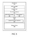
- FIG. 5is a schematic block diagram illustrating one embodiment of a host device in accordance with the present invention.
- FIG. 6is a schematic block diagram illustrating one embodiment of a direct cache module in accordance with the present invention.
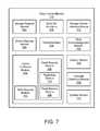
- FIG. 7is a schematic block diagram illustrating another embodiment of a direct cache module in accordance with the present invention.
- FIG. 8is a schematic block diagram illustrating one embodiment of a storage controller in accordance with the present invention.
- FIG. 9is a schematic block diagram illustrating another embodiment of a storage controller in accordance with the present invention.
- FIG. 10is a schematic block diagram illustrating one embodiment of a forward map and a reverse map in accordance with the present invention.
- FIG. 11is a schematic block diagram illustrating one embodiment of a mapping structure, a logical address space of a cache, a sequential, log-based, append-only writing structure, and an address space of a storage device in accordance with the present invention
- FIG. 12is a schematic flow chart diagram illustrating one embodiment of a method for caching data in accordance with the present invention.
- FIG. 13is a schematic flow chart diagram illustrating another embodiment of a method for caching data in accordance with the present invention.
- aspects of the present inventionmay be embodied as a system, method or computer program product. Accordingly, aspects of the present invention may take the form of an entirely hardware embodiment, an entirely software embodiment (including firmware, resident software, micro-code, etc.) or an embodiment combining software and hardware aspects that may all generally be referred to herein as a “circuit,” “module” or “system.” Furthermore, aspects of the present invention may take the form of a computer program product embodied in one or more computer readable medium(s) having computer readable program code embodied thereon.
- modulesmay be implemented as a hardware circuit comprising custom VLSI circuits or gate arrays, off-the-shelf semiconductors such as logic chips, transistors, or other discrete components.
- a modulemay also be implemented in programmable hardware devices such as field programmable gate arrays, programmable array logic, programmable logic devices or the like.
- Modulesmay also be implemented in software for execution by various types of processors.
- An identified module of computer readable program codemay, for instance, comprise one or more physical or logical blocks of computer instructions which may, for instance, be organized as an object, procedure, or function. Nevertheless, the executables of an identified module need not be physically located together, but may comprise disparate instructions stored in different locations which, when joined logically together, comprise the module and achieve the stated purpose for the module.
- a module of computer readable program codemay be a single instruction, or many instructions, and may even be distributed over several different code segments, among different programs, and across several memory devices.
- operational datamay be identified and illustrated herein within modules, and may be embodied in any suitable form and organized within any suitable type of data structure. The operational data may be collected as a single data set, or may be distributed over different locations including over different storage devices, and may exist, at least partially, merely as electronic signals on a system or network.
- the computer readable program codemay be stored and/or propagated on or in one or more computer readable medium(s).
- the computer readable mediummay be a tangible computer readable storage medium storing the computer readable program code.
- the computer readable storage mediummay be, for example, but not limited to, an electronic, magnetic, optical, electromagnetic, infrared, holographic, micromechanical, or semiconductor system, apparatus, or device, or any suitable combination of the foregoing.
- the computer readable mediummay include but are not limited to a portable computer diskette, a hard disk, a random access memory (RAM), a read-only memory (ROM), an erasable programmable read-only memory (EPROM or Flash memory), a portable compact disc read-only memory (CD-ROM), a digital versatile disc (DVD), an optical storage device, a magnetic storage device, a holographic storage medium, a micromechanical storage device, or any suitable combination of the foregoing.
- a computer readable storage mediummay be any tangible medium that can contain, and/or store computer readable program code for use by and/or in connection with an instruction execution system, apparatus, or device.
- the computer readable mediummay also be a computer readable signal medium.
- a computer readable signal mediummay include a propagated data signal with computer readable program code embodied therein, for example, in baseband or as part of a carrier wave. Such a propagated signal may take any of a variety of forms, including, but not limited to, electrical, electro-magnetic, magnetic, optical, or any suitable combination thereof.
- a computer readable signal mediummay be any computer readable medium that is not a computer readable storage medium and that can communicate, propagate, or transport computer readable program code for use by or in connection with an instruction execution system, apparatus, or device.
- Computer readable program code embodied on a computer readable signal mediummay be transmitted using any appropriate medium, including but not limited to wireless, wireline, optical fiber cable, Radio Frequency (RF), or the like, or any suitable combination of the foregoing.
- the computer readable mediummay comprise a combination of one or more computer readable storage mediums and one or more computer readable signal mediums.
- computer readable program codemay be both propagated as an electro-magnetic signal through a fiber optic cable for execution by a processor and stored on RAM storage device for execution by the processor.
- Computer readable program code for carrying out operations for aspects of the present inventionmay be written in any combination of one or more programming languages, including an object oriented programming language such as Java, Smalltalk, C++ or the like and conventional procedural programming languages, such as the “C” programming language or similar programming languages.
- the computer readable program codemay execute entirely on the user's computer, partly on the user's computer, as a stand-alone software package, partly on the user's computer and partly on a remote computer or entirely on the remote computer or server.
- the remote computermay be connected to the user's computer through any type of network, including a local area network (LAN) or a wide area network (WAN), or the connection may be made to an external computer (for example, through the Internet using an Internet Service Provider).
- LANlocal area network
- WANwide area network
- Internet Service Providerfor example, AT&T, MCI, Sprint, EarthLink, MSN, GTE, etc.
- These computer readable program codemay be provided to a processor of a general purpose computer, special purpose computer, sequencer, or other programmable data processing apparatus to produce a machine, such that the instructions, which execute via the processor of the computer or other programmable data processing apparatus, create means for implementing the functions/acts specified in the schematic flowchart diagrams and/or schematic block diagrams block or blocks.
- the computer readable program codemay also be stored in a computer readable medium that can direct a computer, other programmable data processing apparatus, or other devices to function in a particular manner, such that the instructions stored in the computer readable medium produce an article of manufacture including instructions which implement the function/act specified in the schematic flowchart diagrams and/or schematic block diagrams block or blocks.
- the computer readable program codemay also be loaded onto a computer, other programmable data processing apparatus, or other devices to cause a series of operational steps to be performed on the computer, other programmable apparatus or other devices to produce a computer implemented process such that the program code which execute on the computer or other programmable apparatus provide processes for implementing the functions/acts specified in the flowchart and/or block diagram block or blocks.
- each block in the schematic flowchart diagrams and/or schematic block diagramsmay represent a module, segment, or portion of code, which comprises one or more executable instructions of the program code for implementing the specified logical function(s).
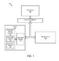
- FIG. 1depicts one embodiment of a system 100 for caching data in accordance with the present invention.
- the system 100in the depicted embodiment, includes a cache 102 a host device 114 , a direct cache module 116 , and a storage device 118 .
- the cache 102in the depicted embodiment, includes a solid-state storage controller 104 , a write data pipeline 106 , a read data pipeline 108 , and a solid-state storage media 110 .
- the system 100caches data for the storage device 118 in the cache 102 .
- the system 100includes a single cache 102 .
- the system 100may include two or more caches 102 .
- the system 100may mirror cached data between several caches 102 , may virtually stripe cached data across multiple caches 102 , or otherwise cache data in more than one cache 102 .
- the cache 102serves as a read and/or a write cache for the storage device 118 and the storage device 118 is a backing store for the cache 102 .
- the cache 102is embodied by a non-volatile, solid-state storage device, with a solid-state storage controller 104 and non-volatile, solid-state storage media 110 .
- the non-volatile, solid-state storage media 110may include flash memory, nano random access memory (“nano RAM or NRAM”), magneto-resistive RAM (“MRAM”), phase change RAM (“PRAM”), etc.
- the cache 102may include other types of non-volatile and/or volatile data storage, such as dynamic RAM (“DRAM”), static RAM (“SRAM”), magnetic data storage, optical data storage, and/or other data storage technologies.
- Embodiments of the cache 102 that include a solid-state storage controller 104 and solid-state storage media 110are described in more detail with respect to FIGS. 2 and 3 .
- the solid-state storage controller 104may mask differences in latency for storage operations performed on the solid-state storage media 110 by grouping erase blocks by access time, wear level, and/or health, by queuing storage operations based on expected completion times, by splitting storage operations, by coordinating storage operation execution in parallel among multiple buses, or the like.
- the cache 102caches data for the storage device 118 .
- the storage device 118in one embodiment, is a backing store associated with the cache 102 and/or with the direct cache module 116 .
- the storage device 118may include a hard disk drive, an optical drive with optical media, a magnetic tape drive, or another type of storage device.
- the storage device 118may have a greater data storage capacity than the cache 102 .
- the storage device 118may have a higher latency, a lower throughput, or the like, than the cache 102 .
- the storage device 118may have a higher latency, a lower throughput, or the like due to properties of the storage device 118 itself, or due to properties of a connection to the storage device 118 .
- the cache 102 and the storage device 118may each include non-volatile, solid-state storage media 110 with similar properties, but the storage device 118 may be in communication with the host device 114 over a data network, while the cache 102 may be directly connected to the host device 114 , causing the storage device 118 to have a higher latency relative to the host 114 than the cache 102 .
- the cache 102 and the storage device 118are in communication with the host device 114 through the direct cache module 116 .
- the cache 102 and/or the storage device 118may be direct attached storage (“DAS”) of the host device 114 .
- DASis data storage that is connected to a device, either internally or externally, without a storage network in between.
- the cache 102 and/or the storage device 118are internal to the host device 114 and are connected using a system bus, such as a peripheral component interconnect express (“PCI-e”) bus, a Serial Advanced Technology Attachment (“SATA”) bus, or the like.
- PCI-eperipheral component interconnect express
- SATASerial Advanced Technology Attachment
- the cache 102 and/or the storage device 118may be external to the host device 114 and may be connected using a universal serial bus (“USB”) connection, an Institute of Electrical and Electronics Engineers (“IEEE”) 1394 bus (“FireWire”), an external SATA (“eSATA”) connection, or the like.
- USBuniversal serial bus
- IEEEInstitute of Electrical and Electronics Engineers
- eSATAexternal SATA
- the cache 102 and/or the storage device 118may be connected to the host device 114 using a peripheral component interconnect (“PCI”) express bus using external electrical or optical bus extension or bus networking solution such as Infiniband or PCI Express Advanced Switching (“PCIe-AS”), or the like.
- PCIe-ASPeripheral Component Interconnect
- the cache 102 and/or the storage device 118may be in the form of a dual-inline memory module (“DIMM”), a daughter card, or a micro-module.
- DIMMdual-inline memory module
- the cache 102 and/or the storage device 118may be elements within a rack-mounted blade.
- the cache 102 and/or the storage device 118may be contained within packages that are integrated directly onto a higher level assembly (e.g. mother board, lap top, graphics processor).
- individual components comprising the cache 102 and/or the storage device 118are integrated directly onto a higher level assembly without intermediate packaging.
- the cache 102includes one or more solid-state storage controllers 104 with a write data pipeline 106 and a read data pipeline 108 , and a solid-state storage media 110 , which are described in more detail below with respect to FIGS. 2 and 3 .
- the cache 102 and/or the storage device 118may be connected to the host device 114 over a data network.
- the cache 102 and/or the storage device 118may include a storage area network (“SAN”) storage device, a network attached storage (“NAS”) device, a network share, or the like.
- the system 100may include a data network, such as the Internet, a wide area network (“WAN”), a metropolitan area network (“MAN”), a local area network (“LAN”), a token ring, a wireless network, a fiber channel network, a SAN, a NAS, ESCON, or the like, or any combination of networks.
- a data networkmay also include a network from the IEEE 802 family of network technologies, such Ethernet, token ring, Wi-Fi, Wi-Max, and the like.
- a data networkmay include servers, switches, routers, cabling, radios, and other equipment used to facilitate networking between the host device 114 and the cache 102 and/or the storage device 118 .
- the cache 102is connected directly to the host device 114 as a DAS device.
- the cache 102is directly connected to the host device 114 as a DAS device and the storage device 118 is directly connected to the cache 102 .
- the cache 102may be connected directly to the host device 114
- the storage device 118may be connected directly to the cache 102 using a direct, wireline connection, such as a PCI express bus, an SATA bus, a USB connection, an IEEE 1394 connection, an eSATA connection, a proprietary direct connection, an external electrical or optical bus extension or bus networking solution such as Infiniband or PCIe-AS, or the like.
- a direct, wireline connectionsuch as a PCI express bus, an SATA bus, a USB connection, an IEEE 1394 connection, an eSATA connection, a proprietary direct connection, an external electrical or optical bus extension or bus networking solution such as Infiniband or PCIe-AS, or the like.
- the system 100includes the host device 114 in communication with the cache 102 and the storage device 118 through the direct cache module 116 .
- a host device 114may be a host, a server, a storage controller of a SAN, a workstation, a personal computer, a laptop computer, a handheld computer, a supercomputer, a computer cluster, a network switch, router, or appliance, a database or storage appliance, a data acquisition or data capture system, a diagnostic system, a test system, a robot, a portable electronic device, a wireless device, or the like.
- the host device 114is in communication with the direct cache module 116 .
- the direct cache module 116receives or otherwise detects read and write requests from the host device 114 for the storage device 118 and manages the caching of data in the cache 102 .
- the direct cache module 116comprises a software application, file system filter driver, or the like.
- the direct cache module 116may include one or more software drivers on the host device 114 , one or more storage controllers, such as the solid-state storage controllers 104 of the cache 102 , a combination of one or more software drivers and storage controllers, or the like.
- hardware and/or software of the direct cache module 116comprises a cache controller that is in communication with the solid-state storage controller 104 to manage operation of the cache 102 .
- the host device 114loads one or more device drivers for the cache 102 and/or the storage device 118 and the direct cache module 116 communicates with the one or more device drivers on the host device 114 .
- the direct cache module 116may communicate directly with a hardware interface of the cache 102 and/or the storage device 118 .
- the direct cache module 116may be integrated with the cache 102 and/or the storage device 118 .
- the cache 102 and/or the storage device 118have block device interfaces that support block device commands.
- the cache 102 and/or the storage device 118may support the standard block device interface, the ATA interface standard, the ATA Packet Interface (“ATAPI”) standard, the small computer system interface (“SCSI”) standard, and/or the Fibre Channel standard which are maintained by the InterNational Committee for Information Technology Standards (“INCITS”).
- the direct cache module 116may interact with the cache 102 and/or the storage device 118 using block device commands to read, write, and clear (or trim) data.
- the direct cache module 116serves as a proxy for the storage device 118 , receiving read and write requests for the storage device 118 directly from the host device 114 .
- the direct cache module 116may represent itself to the host device 114 as a storage device having a capacity similar to and/or matching the capacity of the storage device 118 .
- the direct cache module 116 and/or the solid-state storage controller 104dynamically reduce a cache size for the cache 102 in response to an age characteristic for the solid-state storage media 110 of the cache 102 . For example, as storage elements of the cache 102 age, the direct cache module 116 and/or the solid-state storage controller 104 may remove the storage elements from operation, thereby reducing the cache size for the cache 102 .
- age characteristicsin various embodiments, may include a program/erase count, a bit error rate, an uncorrectable bit error rate, or the like that satisfies a predefined age threshold.
- the direct cache module 116upon receiving a read request or write request from the host device 114 , in one embodiment, fulfills the request by caching write data in the cache 102 or by retrieving read data from one of the cache 102 and the storage device 118 and returning the read data to the host device 114 .
- Data cachesare typically organized into cache lines which divide up the physical capacity of the cache, these cache lines may be divided into several sets.
- a cache lineis typically larger than a block or sector of a backing store associated with a data cache, to provide for prefetching of additional blocks or sectors and to reduce cache misses and increase the cache hit rate.
- Data cachesalso typically evict an entire, fixed size, cache line at a time to make room for newly requested data in satisfying a cache miss.
- Data cachesmay be direct mapped, fully associative, N-way set associative, or the like.
- each block or sector of a backing storehas a one-to-one mapping to a cache line in the direct mapped cache. For example, if a direct mapped cache has T number of cache lines, the backing store associated with the direct mapped cache may be divided into T sections, and the direct mapped cache caches data from a section exclusively in the cache line corresponding to the section. Because a direct mapped cache always caches a block or sector in the same location or cache line, the mapping between a block or sector address and a cache line can be a simple manipulation of an address of the block or sector.
- any cache linecan store data from any block or sector of a backing store.
- a fully associative cachetypically has lower cache miss rates than a direct mapped cache, but has longer hit times (i.e. it takes longer to locate data in the cache) than a direct mapped cache.
- To locate data in a fully associative cacheeither cache tags of the entire cache can be searched, a separate cache index can be used, or the like.
- each sector or block of a backing storemay be cached in any of a set of N different cache lines.
- a 2-way set associative cacheeither of two different cache lines may cache data for a sector or block.
- both the cache and the backing storeare typically divided into sections or sets, with one or more sets of sectors or blocks of the backing store assigned to a set of N cache lines.
- To locate data in an N-way set associative cachea block or sector address is typically mapped to a set of cache lines, and cache tags of the set of cache lines are searched, a separate cache index is searched, or the like to determine which cache line in the set is storing data for the block or sector.
- An N-way set associative cachetypically has miss rates and hit rates between those of a direct mapped cache and those of a fully associative cache.
- the cache 102has characteristics of both a directly mapped cache and a fully associative cache.
- a logical address space of the cache 102in one embodiment, is directly mapped to an address space of the storage device 118 while the physical storage media 110 of the cache 102 is fully associative with regard to the storage device 118 .
- each block or sector of the storage device 118in one embodiment, is directly mapped to a single logical address of the cache 102 while any portion of the physical storage media 110 of the cache 102 may store data for any block or sector of the storage device 118 .
- a logical addressis an identifier of a block of data and is distinct from a physical address of the block of data, but may be mapped to the physical address of the block of data.
- Examples of logical addressesinclude logical block addresses (“LBAs”), logical identifiers, object identifiers, pointers, references, and the like.
- the cache 102has logical or physical cache data blocks associated with each logical address that are equal in size to a block or sector of the storage device 118 .
- the cache 102caches ranges and/or sets of ranges of blocks or sectors for the storage device 118 at a time, providing dynamic or variable length cache line functionality.
- a range or set of ranges of blocks or sectorsmay include a mixture of contiguous and/or noncontiguous blocks.
- the cache 102in one embodiment, supports block device requests that include a mixture of contiguous and/or noncontiguous blocks and that may include “holes” or intervening blocks that the cache 102 does not cache or otherwise store.
- one or more groups of addresses of the storage device 118are directly mapped to corresponding logical addresses of the cache 102 .
- the addresses of the storage device 118may comprise physical addresses or logical addresses.
- Directly mapping logical addresses of the storage device 118 to logical addresses of the cache 102in one embodiment, provides a one-to-one relationship between the logical addresses of the storage device 118 and the logical addresses of the cache 102 .
- Directly mapping logical or physical address space of the storage device 118 to logical addresses of the cache 102precludes the use of an extra translation layer in the direct cache module 116 , such as the use of cache tags, a cache index, the maintenance of a translation data structure, or the like.
- both logical address spacesinclude at least logical addresses 0-N.
- at least a portion of the logical address space of the cache 102represents or appears as the logical address space of the storage device 118 to a client, such as the host device 114 .
- At least a portion of logical addresses in a logical address space of the cache 102may be mapped to physical addresses of the storage device 118 .
- At least a portion of the logical address space of the cache 102in one embodiment, may correspond to the physical address space of the storage device 118 .
- At least a subset of the logical addresses of the cache 102in this embodiment, are directly mapped to corresponding physical addresses of the storage device 118 .
- the logical address space of the cache 102is a sparse address space that is either as large as or is larger than the physical storage capacity of the cache 102 . This allows the storage device 118 to have a larger storage capacity than the cache 102 , while maintaining a direct mapping between the logical addresses of the cache 102 and logical or physical addresses of the storage device 118 .
- the sparse logical address spacemay be thinly provisioned, in one embodiment.
- the cache 102directly maps the logical addresses to distinct physical addresses or locations on the solid-state storage media 110 of the cache 102 , such that the physical addresses or locations of data on the solid-state storage media 110 are fully associative with the storage device 118 .
- the direct cache module 116 and/or the cache 102use the same single mapping structure to map addresses (either logical or physical) of the storage device 118 to logical addresses of the cache 102 and to map logical addresses of the cache 102 to locations/physical addresses of a block or sector (or range of blocks or sectors) on the physical solid state storage media 110 .
- using a single mapping structure for both functionseliminates the need for a separate cache map, cache index, cache tags, or the like, decreasing access times of the cache 102 .
- the solid state storage media 110 in the depicted embodimentare freed to store data for other logical addresses.
- the solid state storage controller 104stores the data at the physical addresses using a log-based, append only writing structure such that data evicted from the cache 102 or overwritten by a subsequent write request invalidates other data in the log. Consequently, a garbage collection process recovers the physical capacity of the invalid data in the log.
- One embodiment of the log-based, append only writing structureis a logically ring-like, cyclic data structure, as new data is appended to the log-based writing structure, previously used physical capacity is reused in a circular, theoretically infinite manner.
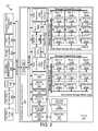
- FIG. 2is a schematic block diagram illustrating one embodiment 201 of a solid-state storage device controller 202 that includes a write data pipeline 106 and a read data pipeline 108 in a cache 102 in accordance with the present invention.
- the solid-state storage device controller 202may be embodied as hardware, as software, or as a combination of hardware and software.
- the solid-state storage device controller 202may include a number of solid-state storage controllers 0-N 104 a - n , each controlling solid-state storage media 110 .
- solid-state controller 0 104 acontrols solid-state storage media 110 a - n .
- solid-state storage controller 0 104 acontrols a data channel so that the attached solid-state storage media 110 a stores data.
- Solid-state storage controller N 104 ncontrols an index metadata channel associated with the stored data and the associated solid-state storage media 110 n stores index metadata.
- the solid-state storage device controller 202includes a single solid-state controller 104 a with a single solid-state storage media 110 a .
- At least one solid-state controller 104is field-programmable gate array (“FPGA”) and controller functions are programmed into the FPGA.
- the FPGAis a Xilinx® FPGA.
- the solid-state storage controller 104comprises components specifically designed as a solid-state storage controller 104 , such as an application-specific integrated circuit (“ASIC”) or custom logic solution.
- ASICapplication-specific integrated circuit
- Each solid-state storage controller 104typically includes a write data pipeline 106 and a read data pipeline 108 , which are describe further in relation to FIG. 3 .
- at least one solid-state storage controller 104is made up of a combination FPGA, ASIC, and custom logic components.
- the solid-state storage media 110is an array of non-volatile solid-state storage elements 216 , 218 , 220 , arranged in banks 214 , and accessed in parallel through a bi-directional storage input/output (“I/O”) bus 210 .
- the storage I/O bus 210in one embodiment, is capable of unidirectional communication at any one time. For example, when data is being written to the solid-state storage media 110 , data cannot be read from the solid-state storage media 110 . In another embodiment, data can flow both directions simultaneously.
- bi-directionalrefers to a data pathway that can have data flowing in only one direction at a time, but when data flowing one direction on the bi-directional data bus is stopped, data can flow in the opposite direction on the bi-directional data bus.
- a solid-state storage element(e.g. SSS 0.0 216 a ) is typically configured as a chip (a package of one or more dies) or a die on a circuit board.
- a solid-state storage element(e.g. 216 a ) operates independently or semi-independently of other solid-state storage elements (e.g. 218 a ) even if these several elements are packaged together in a chip package, a stack of chip packages, or some other package element.
- a column of solid-state storage elements 216 , 218 , 220is designated as a bank 214 .
- each solid-state storage element 216 , 218 , 220is comprised of a single-level cell (“SLC”) devices.
- each solid-state storage element 216 , 218 , 220is comprised of multi-level cell (“MLC”) devices.
- solid-state storage elements for multiple banks that share a common storage I/O bus 210 a roware packaged together.
- a solid-state storage element 216 , 218 , 220may have one or more dies per chip with one or more chips stacked vertically and each die may be accessed independently.
- a solid-state storage elemente.g. SSS 0.0 216 a
- SSS 0.0 216 amay have one or more virtual dies per die and one or more dies per chip and one or more chips stacked vertically and each virtual die may be accessed independently.
- a solid-state storage element SSS 0.0 216 amay have one or more virtual dies per die and one or more dies per chip with some or all of the one or more dies stacked vertically and each virtual die may be accessed independently.
- two diesare stacked vertically with four stacks per group to form eight storage elements (e.g. SSS 0.0-SSS 0.8) 216 a - 220 a , each in a separate bank 214 a - n .
- 20 storage elements (e.g. SSS 0.0-SSS 20.0) 216form a virtual bank 214 a so that each of the eight virtual banks has 20 storage elements (e.g. SSS0.0-SSS 20.8).
- Datais sent to the solid-state storage media 110 over the storage I/O bus 210 to all storage elements of a particular group of storage elements (SSS 0.0-SSS 0.8) 216 a , 218 a , 220 a .
- the storage control bus 212 ais used to select a particular bank (e.g. Bank-0 214 a ) so that the data received over the storage I/O bus 210 connected to all banks 214 is written just to the selected bank 214 a.
- the storage control bus 212 and storage I/O bus 210are used together by the solid-state controller 104 to communicate addressing information, storage element command information, and data to be stored.
- this address, data, and command informationmay be communicated using one or the other of these buses 212 , 210 , or using separate buses for each type of control information.
- addressing information, storage element command information, and storage datatravel on the storage I/O bus 210 and the storage control bus 212 carries signals for activating a bank as well as identifying whether the data on the storage I/O bus 210 lines constitute addressing information, storage element command information, or storage data.
- a control signal on the storage control bus 212such as “command enable” may indicate that the data on the storage I/O bus 210 lines is a storage element command such as program, erase, reset, read, and the like.
- a control signal on the storage control bus 212such as “address enable” may indicate that the data on the storage I/O bus 210 lines is addressing information such as erase block identifier, page identifier, and optionally offset within the page within a particular storage element.
- an absence of a control signal on the storage control bus 212 for both “command enable” and “address enable”may indicate that the data on the storage I/O bus 210 lines is storage data that is to be stored on the storage element at a previously addressed erase block, physical page, and optionally offset within the page of a particular storage element.
- the storage I/O bus 210is comprised of one or more independent I/O buses (“IIOBa-m” comprising 210 a.a - m , 210 n.a - m ) wherein the solid-state storage elements within each row share one of the independent I/O buses across each solid-state storage element 216 , 218 , 220 in parallel so that all banks 214 are accessed simultaneously.
- IIOBa-mindependent I/O buses
- a second IIOB 210 a.b of the storage I/O bus 210may access a second solid-state storage element 216 b , 218 b , 220 b of each bank 214 a - n simultaneously. Each row of solid-state storage elements 216 , 218 , 220 is accessed simultaneously. In one embodiment, where solid-state storage elements 216 , 218 , 220 are multi-level (physically stacked), all physical levels of the solid-state storage elements 216 , 218 , 220 are accessed simultaneously. As used herein, “simultaneously” also includes near simultaneous access where devices are accessed at slightly different intervals to avoid switching noise. Simultaneously is used in this context to be distinguished from a sequential or serial access wherein commands and/or data are sent individually one after the other.
- banks 214 a - nare independently selected using the storage control bus 212 .
- a bank 214is selected using a chip enable or chip select. Where both chip select and chip enable are available, the storage control bus 212 may select one level of a multi-level solid-state storage element 216 , 218 , 220 using either of the chip select signal and the chip enable signal. In other embodiments, other commands are used by the storage control bus 212 to individually select one level of a multi-level solid-state storage element 216 , 218 , 220 .
- Solid-state storage elements 216 , 218 , 220may also be selected through a combination of control and of address information transmitted on storage I/O bus 210 and the storage control bus 212 .
- each solid-state storage element 216 , 218 , 220is partitioned into erase blocks and each erase block is partitioned into pages.
- a typical pageis 2000 bytes (“2 kB”).
- a solid-state storage elemente.g. SSS0.0
- SSS0.0includes two registers and can program two pages so that a two-register solid-state storage element has a page size of 4 kB.
- a single bank 214 a of 20 solid-state storage elements 216 a - mwould then have an 80 kB capacity of pages accessed with the same address going out of the storage I/O bus 210 .
- This group of pages in a bank 214 of solid-state storage elements 216 , 218 , 220 of 80 kBmay be called a logical or virtual page.
- an erase block of each storage element 216 a - m of a bank 214 amay be grouped to form a logical erase block.
- erasing a logical erase blockcauses a physical erase block of each storage element 216 a - m of a bank 214 a to be erased.
- an erase block of pages within a solid-state storage element 216 , 218 , 220is erased when an erase command is received within a solid-state storage element 216 , 218 , 220 .
- a single physical erase block on each storage elementcollectively forms a logical erase block for the solid-state storage media 110 a .
- erasing a logical erase blockcomprises erasing an erase block at the same address within each storage element (e.g. SSS M.N) in the solid-state storage media 110 a .
- the size and number of erase blocks, pages, planes, or other logical and physical divisions within a solid-state storage element 216 , 218 , 220may change over time with advancements in technology, it is to be expected that many embodiments consistent with new configurations are possible and are consistent with the general description herein.
- datais written in packets to the storage elements.
- the solid-state controller 104uses the storage I/O bus 210 and storage control bus 212 to address a particular bank 214 , storage element 216 , 218 , 220 , physical erase block, physical page, and optionally offset within a physical page for writing the data packet.
- the solid-state controller 104sends the address information for the data packet by way of the storage I/O bus 210 and signals that the data on the storage I/O bus 210 is address data by way of particular signals set on the storage control bus 212 .
- the solid-state controller 104follows the transmission of the address information with transmission of the data packet of data that is to be stored.
- the physical addresscontains enough information for the solid-state storage element 216 , 218 , 220 to direct the data packet to the designated location within the page.
- the storage I/O bus 210 a.aconnects to each storage element in a row of storage elements (e.g. SSS 0.0-SSS 0.N 216 a , 218 a , 220 a ).
- the solid-state controller 104 aactivates a desired bank 214 a using the storage control bus 212 a , such that data on storage I/O bus 210 a.a reaches the proper page of a single storage element (e.g. SSS 0.0 216 a ).
- the solid-state controller 104 asimultaneously activates the same bank 214 a using the storage control bus 212 a , such that different data (a different data packet) on storage I/O bus 210 a.b reaches the proper page of a single storage element on another row (e.g. SSS 1.0 216 b ). In this manner, multiple physical pages of multiple storage elements 216 , 218 , 220 may be written to simultaneously within a single bank 214 to store a logical page.
- a read commandmay require a command on the storage control bus 212 to select a single bank 214 a and the appropriate page within that bank 214 a .
- a read commandreads an entire physical page from each storage element, and because there are multiple solid-state storage elements 216 , 218 , 220 in parallel in a bank 214 , an entire logical page is read with a read command.
- the read commandmay be broken into subcommands, as will be explained below with respect to bank interleave.
- a logical pagemay also be accessed in a write operation.
- a solid-state controller 104may send an erase block erase command over all the lines of the storage I/O bus 210 to erase a physical erase block having a particular erase block address.
- the solid-state controller 104may simultaneously activate a single bank 214 using the storage control bus 212 such that each physical erase block in the single activated bank 214 is erased as part of a logical erase block.
- the solid-state controller 104may send an erase block erase command over all the lines of the storage I/O bus 210 to erase a physical erase block having a particular erase block address on each storage element 216 , 218 , 220 (SSS 0.0-SSS M.N). These particular physical erase blocks together may form a logical erase block. Once the address of the physical erase blocks is provided to the storage elements 216 , 218 , 220 , the solid-state controller 104 may initiate the erase command on a bank 214 a by bank 214 b by bank 214 n basis (either in order or based on some other sequence). Other commands may also be sent to a particular location using a combination of the storage I/O bus 210 and the storage control bus 212 . One of skill in the art will recognize other ways to select a particular storage location using the bi-directional storage I/O bus 210 and the storage control bus 212 .
- the storage controller 104sequentially writes data on the solid-state storage media 110 in a log structured format and within one or more physical structures of the storage elements, the data is sequentially stored on the solid-state storage media 110 .
- Sequentially writing datainvolves the storage controller 104 streaming data packets into storage write buffers for storage elements, such as a chip (a package of one or more dies) or a die on a circuit board.
- the storage write buffersare full, the data packets are programmed to a designated virtual or logical page (“LP”).
- LPvirtual or logical page
- Data packetsthen refill the storage write buffers and, when full, the data packets are written to the next LP.
- the next virtual pagemay be in the same bank 214 a or another bank (e.g. 214 b ). This process continues, LP after LP, typically until a virtual or logical erase block (“LEB”) is filled.
- LEBvirtual or logical erase block
- the streamingmay continue across LEB boundaries with the process continuing, LEB after LEB.
- the storage controller 104sequentially stores data packets in an LEB by order of processing.
- the storage controller 104stores packets in the order that they come out of the write data pipeline 106 . This order may be a result of data segments arriving from a requesting device mixed with packets of valid data that are being read from another storage location as valid data is being recovered from another LEB during a recovery operation.
- the sequentially stored datacan serve as a log to reconstruct data indexes and other metadata using information from data packet headers.
- the storage controller 104may reconstruct a storage index by reading headers to determine the data structure to which each packet belongs and sequence information to determine where in the data structure the data or metadata belongs.
- the storage controller 104uses physical address information for each packet and timestamp or sequence information to create a mapping between the physical locations of the packets and the data structure identifier and data segment sequence. Timestamp or sequence information is used by the storage controller 104 to replay the sequence of changes made to the index and thereby reestablish the most recent state.
- erase blocksare time stamped or given a sequence number as packets are written and the timestamp or sequence information of an erase block is used along with information gathered from container headers and packet headers to reconstruct the storage index.
- timestamp or sequence informationis written to an erase block when the erase block is recovered.
- a read, modify, write operationdata packets associated with the logical structure are located and read in a read operation.
- Data segments of the modified structure that have been modifiedare not written to the location from which they are read. Instead, the modified data segments are again converted to data packets and then written to the next available location in the virtual page currently being written.
- Index entries for the respective data packetsare modified to point to the packets that contain the modified data segments.
- the entry or entries in the index for data packets associated with the same logical structure that have not been modifiedwill include pointers to original location of the unmodified data packets.
- the original logical structureis maintained, for example to maintain a previous version of the logical structure, the original logical structure will have pointers in the index to all data packets as originally written.
- the new logical structurewill have pointers in the index to some of the original data packets and pointers to the modified data packets in the virtual page that is currently being written.
- the indexincludes an entry for the original logical structure mapped to a number of packets stored on the solid-state storage media 110 .
- a new logical structureis created and a new entry is created in the index mapping the new logical structure to the original packets.
- the new logical structureis also written to the solid-state storage media 110 with its location mapped to the new entry in the index.
- the new logical structure packetsmay be used to identify the packets within the original logical structure that are referenced in case changes have been made in the original logical structure that have not been propagated to the copy and the index is lost or corrupted.
- the indexincludes a logical entry for a logical block.
- sequentially writing packetsfacilitates a more even use of the solid-state storage media 110 and allows the solid-storage device controller 202 to monitor storage hot spots and level usage of the various virtual pages in the solid-state storage media 110 .
- Sequentially writing packetsalso facilitates a powerful, efficient garbage collection system, which is described in detail below.
- One of skill in the artwill recognize other benefits of sequential storage of data packets.
- the system 100may comprise a log-structured storage system or log-structured array similar to a log-structured file system and the order that data is stored may be used to recreate an index.
- an index that includes a logical-to-physical mappingis stored in volatile memory. If the index is corrupted or lost, the index may be reconstructed by addressing the solid-state storage media 110 in the order that the data was written.
- a logical erase block (“LEB”)data is typically stored sequentially by filling a first logical page, then a second logical page, etc. until the LEB is filled.
- the solid-state storage controller 104then chooses another LEB and the process repeats.
- the indexcan be rebuilt by traversing the solid-state storage media 110 in order from beginning to end.
- the solid-state storage controller 104may only need to replay a portion of the solid-state storage media 110 to rebuild a portion of the index that was not stored in non-volatile memory.
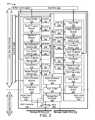
- the solid-state storage device controller 202also includes a data bus 204 , a local bus 206 , a buffer controller 208 , buffers 0-N 222 a - n , a master controller 224 , a direct memory access (“DMA”) controller 226 , a memory controller 228 , a dynamic memory array 230 , a static random memory array 232 , a management controller 234 , a management bus 236 , a bridge 238 to a system bus 240 , and miscellaneous logic 242 , which are described below.
- DMAdirect memory access
- the system bus 240is coupled to one or more network interface cards (“NICs”) 244 , some of which may include remote DMA (“RDMA”) controllers 246 , one or more central processing unit (“CPU”) 248 , one or more external memory controllers 250 and associated external memory arrays 252 , one or more storage controllers 254 , peer controllers 256 , and application specific processors 258 , which are described below.
- NICsnetwork interface cards
- RDMAremote DMA
- CPUcentral processing unit
- external memory controllers 250 and associated external memory arrays 252one or more storage controllers 254
- peer controllers 256peer controllers 256
- application specific processors 258application specific processors
- the solid-state storage controller(s) 104communicate data to the solid-state storage media 110 over a storage I/O bus 210 .
- the storage I/O bus 210comprises an array of busses, one for each row of storage elements 216 , 218 , 220 spanning the banks 214 .
- the term “storage I/O bus”may refer to one storage I/O bus 210 or an array of data independent busses 204 .
- each storage I/O bus 210accessing a row of storage elements (e.g.
- 216 a , 218 a , 220 amay include a logical-to-physical mapping for storage divisions (e.g. erase blocks) accessed in a row of storage elements 216 a , 218 a , 220 a .
- This mappingallows a logical address mapped to a physical address of a storage division to be remapped to a different storage division if the first storage division fails, partially fails, is inaccessible, or has some other problem. Remapping is explained further in relation to the remapping module 430 of FIG. 4 .
- Datamay also be communicated to the solid-state storage controller(s) 104 from a requesting device 155 through the system bus 240 , bridge 238 , local bus 206 , buffer(s) 222 , and finally over a data bus 204 .
- the data bus 204typically is connected to one or more buffers 222 a - n controlled with a buffer controller 208 .
- the buffer controller 208typically controls transfer of data from the local bus 206 to the buffers 222 and through the data bus 204 to the pipeline input buffer 306 and output buffer 330 .
- the buffer controller 208typically controls how data arriving from a requesting device 155 can be temporarily stored in a buffer 222 and then transferred onto a data bus 204 , or vice versa, to account for different clock domains, to prevent data collisions, etc.
- the buffer controller 208typically works in conjunction with the master controller 224 to coordinate data flow. As data arrives, the data will arrive on the system bus 240 , be transferred to the local bus 206 through a bridge 238 .
- the datais transferred from the local bus 206 to one or more data buffers 222 as directed by the master controller 224 and the buffer controller 208 .
- the datathen flows out of the buffer(s) 222 to the data bus 204 , through a solid-state controller 104 , and on to the solid-state storage media 110 such as NAND flash or other storage media.
- data and associated out-of-band metadata (“metadata”) arriving with the datais communicated using one or more data channels comprising one or more solid-state storage controllers 104 a - 104 n ⁇ 1 and associated solid-state storage media 110 a - 110 n ⁇ 1 while at least one channel (solid-state storage controller 104 n , solid-state storage media 110 n ) is dedicated to in-band metadata, such as index information and other metadata generated internally to the cache 102 .
- the local bus 206is typically a bidirectional bus or set of busses that allows for communication of data and commands between devices internal to the solid-state storage device controller 202 and between devices internal to the cache 102 and devices 244 - 258 connected to the system bus 240 .
- the bridge 238facilitates communication between the local bus 206 and system bus 240 .
- One of skill in the artwill recognize other embodiments such as ring structures or switched star configurations and functions of buses 240 , 206 , 204 and bridges 238 .
- the system bus 240is typically a bus of a host device 114 or other device in which the cache 102 is installed or connected.
- the system bus 240may be a PCI-e bus, a Serial Advanced Technology Attachment (“serial ATA”) bus, parallel ATA, or the like.
- the system bus 240is an external bus such as small computer system interface (“SCSI”), FireWire, Fiber Channel, USB, PCIe-AS, or the like.
- SCSIsmall computer system interface
- FireWireFireWire
- Fiber ChannelUniversal Serial Bus
- USBPeripheral Component Interconnect Express
- the solid-state storage device controller 202includes a master controller 224 that controls higher-level functions within the cache 102 .
- the master controller 224controls data flow by interpreting requests, directs creation of indexes to map identifiers associated with data to physical locations of associated data, coordinating DMA requests, etc. Many of the functions described herein are controlled wholly or in part by the master controller 224 .
- the master controller 224uses embedded controller(s). In another embodiment, the master controller 224 uses local memory such as a dynamic memory array 230 (dynamic random access memory “DRAM”), a static memory array 232 (static random access memory “SRAM”), etc. In one embodiment, the local memory is controlled using the master controller 224 . In another embodiment, the master controller 224 accesses the local memory via a memory controller 228 . In another embodiment, the master controller 224 runs a Linux server and may support various common server interfaces, such as the World Wide Web, hyper-text markup language (“HTML”), etc. In another embodiment, the master controller 224 uses a nano-processor. The master controller 224 may be constructed using programmable or standard logic, or any combination of controller types listed above. The master controller 224 may be embodied as hardware, as software, or as a combination of hardware and software. One skilled in the art will recognize many embodiments for the master controller 224 .
- DRAMdynamic random access memory
- SRAMstatic memory array 232
- the local memoryis
- the master controller 224divides the work load among internal controllers, such as the solid-state storage controllers 104 a - n .
- the master controller 224may divide a data structure to be written to the data storage devices (e.g. solid-state storage media 110 a - n ) so that a portion of the data structure is stored on each of the attached data storage devices. This feature is a performance enhancement allowing quicker storage and access to a data structure.
- the master controller 224is implemented using an FPGA.
- the firmware within the master controller 224may be updated through the management bus 236 , the system bus 240 over a network connected to a NIC 244 or other device connected to the system bus 240 .
- the master controller 224emulates block storage such that a host device 114 or other device connected to the storage device/cache 102 views the storage device/cache 102 as a block storage device and sends data to specific physical or logical addresses in the storage device/cache 102 .
- the master controller 224then divides up the blocks and stores the data blocks.
- the master controller 224maps the blocks and physical or logical address sent with the block to the actual locations determined by the master controller 224 . The mapping is stored in the index.
- a block device application program interface (“API”)is provided in a driver in the host device 114 , or other device wishing to use the storage device/cache 102 as a block storage device.
- APIapplication program interface
- the master controller 224coordinates with NIC controllers 244 and embedded RDMA controllers 246 to deliver just-in-time RDMA transfers of data and command sets.
- NIC controller 244may be hidden behind a non-transparent port to enable the use of custom drivers.
- a driver on a host device 114may have access to a computer network through an I/O memory driver using a standard stack API and operating in conjunction with NICs 244 .
- the master controller 224is also a redundant array of independent drive (“RAID”) controller. Where the data storage device/cache 102 is networked with one or more other data storage devices, the master controller 224 may be a RAID controller for single tier RAID, multi-tier RAID, progressive RAID, etc. The master controller 224 may also allows some objects and other data structures to be stored in a RAID array and other data structures to be stored without RAID. In another embodiment, the master controller 224 may be a distributed RAID controller element. In another embodiment, the master controller 224 may comprise many RAID, distributed RAID, and other functions as described elsewhere.
- RAIDredundant array of independent drive
- the master controller 224coordinates with single or redundant network managers (e.g. switches) to establish routing, to balance bandwidth utilization, failover, etc.
- the master controller 224coordinates with integrated application specific logic (via local bus 206 ) and associated driver software.
- the master controller 224coordinates with attached application specific processors 258 or logic (via the external system bus 240 ) and associated driver software.
- the master controller 224coordinates with remote application specific logic (via a computer network) and associated driver software.
- the master controller 224coordinates with the local bus 206 or external bus attached hard disk drive (“HDD”) storage controller.
- HDDhard disk drive
- the master controller 224communicates with one or more storage controllers 254 where the storage device/cache 102 may appear as a storage device connected through a SCSI bus, Internet SCSI (“iSCSI”), fiber channel, etc. Meanwhile the storage device/cache 102 may autonomously manage objects or other data structures and may appear as an object file system or distributed object file system.
- the master controller 224may also be accessed by peer controllers 256 and/or application specific processors 258 .
- the master controller 224coordinates with an autonomous integrated management controller to periodically validate FPGA code and/or controller software, validate FPGA code while running (reset) and/or validate controller software during power on (reset), support external reset requests, support reset requests due to watchdog timeouts, and support voltage, current, power, temperature, and other environmental measurements and setting of threshold interrupts.
- the master controller 224manages garbage collection to free erase blocks for reuse.
- the master controller 224manages wear leveling.
- the master controller 224allows the data storage device/cache 102 to be partitioned into multiple virtual devices and allows partition-based media encryption.
- the master controller 224supports a solid-state storage controller 104 with advanced, multi-bit ECC correction.
- One of skill in the artwill recognize other features and functions of a master controller 224 in a storage controller 152 , or more specifically in a cache 102 .
- the solid-state storage device controller 202includes a memory controller 228 which controls a dynamic random memory array 230 and/or a static random memory array 232 .
- the memory controller 228may be independent or integrated with the master controller 224 .
- the memory controller 228typically controls volatile memory of some type, such as DRAM (dynamic random memory array 230 ) and SRAM (static random memory array 232 ).
- the memory controller 228also controls other memory types such as electrically erasable programmable read only memory (“EEPROM”), etc.
- EEPROMelectrically erasable programmable read only memory
- the memory controller 228controls two or more memory types and the memory controller 228 may include more than one controller.
- the memory controller 228controls as much SRAM 232 as is feasible and by DRAM 230 to supplement the SRAM 232 .
- the logical-to-physical indexis stored in memory 230 , 232 and then periodically off-loaded to a channel of the solid-state storage media 110 n or other non-volatile memory.
- the memory controller 228dynamic memory array 230
- static memory array 232static memory array
- the solid-state storage device controller 202includes a DMA controller 226 that controls DMA operations between the storage device/cache 102 and one or more external memory controllers 250 and associated external memory arrays 252 and CPUs 248 .
- the external memory controllers 250 and external memory arrays 252are called external because they are external to the storage device/cache 102 .
- the DMA controller 226may also control RDMA operations with requesting devices through a NIC 244 and associated RDMA controller 246 .
- the solid-state storage device controller 202includes a management controller 234 connected to a management bus 236 .
- the management controller 234manages environmental metrics and status of the storage device/cache 102 .
- the management controller 234may monitor device temperature, fan speed, power supply settings, etc. over the management bus 236 .
- the management controller 234may support the reading and programming of erasable programmable read only memory (“EEPROM”) for storage of FPGA code and controller software.
- EEPROMerasable programmable read only memory
- the management bus 236is connected to the various components within the storage device/cache 102 .
- the management controller 234may communicate alerts, interrupts, etc. over the local bus 206 or may include a separate connection to a system bus 240 or other bus.
- the management bus 236is an Inter-Integrated Circuit (“I2C”) bus.
- I2CInter-Integrated Circuit
- the solid-state storage device controller 202includes miscellaneous logic 242 that may be customized for a specific application. Typically where the solid-state device controller 202 or master controller 224 is/are configured using a FPGA or other configurable controller, custom logic may be included based on a particular application, customer requirement, storage requirement, etc.
- FIG. 3is a schematic block diagram illustrating one embodiment 300 of a solid-state storage controller 104 with a write data pipeline 106 and a read data pipeline 108 in a cache 102 in accordance with the present invention.
- the embodiment 300includes a data bus 204 , a local bus 206 , and buffer control 208 , which are substantially similar to those described in relation to the solid-state storage device controller 202 of FIG. 2 .
- the write data pipeline 106includes a packetizer 302 and an error-correcting code (“ECC”) generator 304 .
- ECCerror-correcting code
- the write data pipeline 106includes an input buffer 306 , a write synchronization buffer 308 , a write program module 310 , a compression module 312 , an encryption module 314 , a garbage collector bypass 316 (with a portion within the read data pipeline 108 ), a media encryption module 318 , and a write buffer 320 .
- the read data pipeline 108includes a read synchronization buffer 328 , an ECC correction module 322 , a depacketizer 324 , an alignment module 326 , and an output buffer 330 .
- the read data pipeline 108may include a media decryption module 332 , a portion of the garbage collector bypass 316 , a decryption module 334 , a decompression module 336 , and a read program module 338 .
- the solid-state storage controller 104may also include control and status registers 340 and control queues 342 , a bank interleave controller 344 , a synchronization buffer 346 , a storage bus controller 348 , and a multiplexer (“MUX”) 350 .
- MUXmultiplexer
- the write data pipeline 106includes a packetizer 302 that receives a data or metadata segment to be written to the solid-state storage, either directly or indirectly through another write data pipeline 106 stage, and creates one or more packets sized for the solid-state storage media 110 .
- the data or metadata segmentis typically part of a data structure such as an object, but may also include an entire data structure. In another embodiment, the data segment is part of a block of data, but may also include an entire block of data.
- a set of datasuch as a data structure is received from a computer such as the host device 114 , or other computer or device and is transmitted to the cache 102 in data segments streamed to the cache 102 and/or the host device 114 .
- a data segmentmay also be known by another name, such as data parcel, but as referenced herein includes all or a portion of a data structure or data block.
- Each data structureis stored as one or more packets.
- Each data structuremay have one or more container packets.
- Each packetcontains a header.
- the headermay include a header type field. Type fields may include data, attribute, metadata, data segment delimiters (multi-packet), data structures, data linkages, and the like.
- the headermay also include information regarding the size of the packet, such as the number of bytes of data included in the packet. The length of the packet may be established by the packet type.
- the headermay include information that establishes the relationship of the packet to a data structure. An example might be the use of an offset in a data packet header to identify the location of the data segment within the data structure.
- One of skill in the artwill recognize other information that may be included in a header added to data by a packetizer 302 and other information that may be added to a data packet.
- Each packetincludes a header and possibly data from the data or metadata segment.
- the header of each packetincludes pertinent information to relate the packet to the data structure to which the packet belongs.
- the headermay include an object identifier or other data structure identifier and offset that indicate the data segment, object, data structure or data block from which the data packet was formed.
- the headermay also include a logical address used by the storage bus controller 348 to store the packet.
- the headermay also include information regarding the size of the packet, such as the number of bytes included in the packet.
- the headermay also include a sequence number that identifies where the data segment belongs with respect to other packets within the data structure when reconstructing the data segment or data structure.
- the headermay include a header type field.
- Type fieldsmay include data, data structure attributes, metadata, data segment delimiters (multi-packet), data structure types, data structure linkages, and the like.
- data segment delimitersmulti-packet
- data structure typesdata structure linkages, and the like.
- packetizer 302One of skill in the art will recognize other information that may be included in a header added to data or metadata by a packetizer 302 and other information that may be added to a packet.
- the write data pipeline 106includes an ECC generator 304 that that generates one or more error-correcting codes (“ECC”) for the one or more packets received from the packetizer 302 .
- the ECC generator 304typically uses an error correcting algorithm to generate ECC check bits which are stored with the one or more data packets.
- the ECC codes generated by the ECC generator 304 together with the one or more data packets associated with the ECC codescomprise an ECC chunk.
- the ECC data stored with the one or more data packetsis used to detect and to correct errors introduced into the data through transmission and storage.
- packetsare streamed into the ECC generator 304 as un-encoded blocks of length N.
- a syndrome of length Sis calculated, appended and output as an encoded block of length N+S.
- N and Sare dependent upon the characteristics of the algorithm which is selected to achieve specific performance, efficiency, and robustness metrics.
- ECC algorithmsare not dynamically modified.
- the ECC data stored with the data packetsis robust enough to correct errors in more than two bits.
- the life of the solid-state storage media 110allows the life of the solid-state storage media 110 to be extended.
- the flash memorymay be written approximately 100,000 times without error per erase cycle. This usage limit may be extended using a robust ECC algorithm.
- the cache 102can internally correct errors and has a longer useful life than if a less robust ECC algorithm is used, such as single bit correction.
- the ECC generator 304may use a less robust algorithm and may correct single-bit or double-bit errors.
- the solid-state storage device 110may comprise less reliable storage such as multi-level cell (“MLC”) flash in order to increase capacity, which storage may not be sufficiently reliable without more robust ECC algorithms.
- MLCmulti-level cell
- the write pipeline 106includes an input buffer 306 that receives a data segment to be written to the solid-state storage media 110 and stores the incoming data segments until the next stage of the write data pipeline 106 , such as the packetizer 302 (or other stage for a more complex write data pipeline 106 ) is ready to process the next data segment.
- the input buffer 306typically allows for discrepancies between the rate data segments are received and processed by the write data pipeline 106 using an appropriately sized data buffer.
- the input buffer 306also allows the data bus 204 to transfer data to the write data pipeline 106 at rates greater than can be sustained by the write data pipeline 106 in order to improve efficiency of operation of the data bus 204 .
- a buffering functionis performed elsewhere, such as in the cache 102 , but outside the write data pipeline 106 , in the host device 114 , such as within a network interface card (“NIC”), or at another device, for example when using remote direct memory access (“RDMA”).
- NICnetwork interface card
- RDMAremote direct memory access
- the write data pipeline 106also includes a write synchronization buffer 308 that buffers packets received from the ECC generator 304 prior to writing the packets to the solid-state storage media 110 .
- the write synch buffer 308is located at a boundary between a local clock domain and a solid-state storage clock domain and provides buffering to account for the clock domain differences.
- synchronous solid-state storage media 110may be used and synchronization buffers 308 328 may be eliminated.
- the write data pipeline 106also includes a media encryption module 318 that receives the one or more packets from the packetizer 302 , either directly or indirectly, and encrypts the one or more packets using an encryption key unique to the cache 102 prior to sending the packets to the ECC generator 304 .
- the entire packetis encrypted, including the headers.
- headersare not encrypted.
- encryption keyis understood to mean a secret encryption key that is managed externally from a solid-state storage controller 104 .
- the media encryption module 318 and corresponding media decryption module 332provide a level of security for data stored in the solid-state storage media 110 .
- datais encrypted with the media encryption module 318
- the solid-state storage media 110is connected to a different solid-state storage controller 104 , cache 102 , or server, the contents of the solid-state storage media 110 typically could not be read without use of the same encryption key used during the write of the data to the solid-state storage media 110 without significant effort.
- the cache 102does not store the encryption key in non-volatile storage and allows no external access to the encryption key.
- the encryption keyis provided to the solid-state storage controller 104 during initialization.
- the cache 102may use and store a non-secret cryptographic nonce that is used in conjunction with an encryption key. A different nonce may be stored with every packet. Data segments may be split between multiple packets with unique nonces for the purpose of improving protection by the encryption algorithm.
- the encryption keymay be received from a host device 114 , a server, key manager, or other device that manages the encryption key to be used by the solid-state storage controller 104 .
- the solid-state storage media 110may have two or more partitions and the solid-state storage controller 104 behaves as though it was two or more solid-state storage controllers 104 , each operating on a single partition within the solid-state storage media 110 .
- a unique media encryption keymay be used with each partition.
- the write data pipeline 106also includes an encryption module 314 that encrypts a data or metadata segment received from the input buffer 306 , either directly or indirectly, prior sending the data segment to the packetizer 302 , the data segment encrypted using an encryption key received in conjunction with the data segment.
- the encryption keys used by the encryption module 314 to encrypt datamay not be common to all data stored within the cache 102 but may vary on a per data structure basis and received in conjunction with receiving data segments as described below. For example, an encryption key for a data segment to be encrypted by the encryption module 314 may be received with the data segment or may be received as part of a command to write a data structure to which the data segment belongs.
- the cache 102may use and store a non-secret cryptographic nonce in each data structure packet that is used in conjunction with the encryption key.
- a different noncemay be stored with every packet.
- Data segmentsmay be split between multiple packets with unique nonces for the purpose of improving protection by the encryption algorithm.
- the encryption keymay be received from a host device 114 , a computer, key manager, or other device that holds the encryption key to be used to encrypt the data segment.
- encryption keysare transferred to the solid-state storage controller 104 from one of a cache 102 , a computer, a host device 114 , or other external agent which has the ability to execute industry standard methods to securely transfer and protect private and public keys.
- the encryption module 314encrypts a first packet with a first encryption key received in conjunction with the packet and encrypts a second packet with a second encryption key received in conjunction with the second packet. In another embodiment, the encryption module 314 encrypts a first packet with a first encryption key received in conjunction with the packet and passes a second data packet on to the next stage without encryption.
- the encryption module 314 included in the write data pipeline 106 of the cache 102allows data structure-by-data structure or segment-by-segment data encryption without a single file system or other external system to keep track of the different encryption keys used to store corresponding data structures or data segments.
- Each requesting device 155 or related key managerindependently manages encryption keys used to encrypt only the data structures or data segments sent by the requesting device 155 .
- the encryption module 314may encrypt the one or more packets using an encryption key unique to the cache 102 .
- the encryption module 314may perform this media encryption independently, or in addition to the encryption described above.
- the entire packetis encrypted, including the headers.
- headersare not encrypted.
- the media encryption by the encryption module 314provides a level of security for data stored in the solid-state storage media 110 .
- the contents of the solid-state storage media 110typically could not be read without use of the same encryption key used during the write of the data to the solid-state storage media 110 without significant effort.
- the write data pipeline 106includes a compression module 312 that compresses the data for metadata segment prior to sending the data segment to the packetizer 302 .
- the compression module 312typically compresses a data or metadata segment using a compression routine known to those of skill in the art to reduce the storage size of the segment. For example, if a data segment includes a string of 512 zeros, the compression module 312 may replace the 512 zeros with code or token indicating the 512 zeros where the code is much more compact than the space taken by the 512 zeros.
- the compression module 312compresses a first segment with a first compression routine and passes along a second segment without compression. In another embodiment, the compression module 312 compresses a first segment with a first compression routine and compresses the second segment with a second compression routine. Having this flexibility within the cache 102 is beneficial so that the host device 114 or other devices writing data to the cache 102 may each specify a compression routine or so that one can specify a compression routine while another specifies no compression. Selection of compression routines may also be selected according to default settings on a per data structure type or data structure class basis.
- a first data structure of a specific data structuremay be able to override default compression routine settings and a second data structure of the same data structure class and data structure type may use the default compression routine and a third data structure of the same data structure class and data structure type may use no compression.
- the write data pipeline 106includes a garbage collector bypass 316 that receives data segments from the read data pipeline 108 as part of a data bypass in a garbage collection system.
- a garbage collection systemtypically marks packets that are no longer valid, typically because the packet is marked for deletion or has been modified and the modified data is stored in a different location.
- the garbage collection systemdetermines that a particular section of storage may be recovered. This determination may be due to a lack of available storage capacity, the percentage of data marked as invalid reaching a threshold, a consolidation of valid data, an error detection rate for that section of storage reaching a threshold, or improving performance based on data distribution, etc. Numerous factors may be considered by a garbage collection algorithm to determine when a section of storage is to be recovered.
- the garbage collector bypass 316allows packets to be read into the read data pipeline 108 and then transferred directly to the write data pipeline 106 without being routed out of the solid-state storage controller 104 .
- the garbage collector bypass 316is part of an autonomous garbage collector system that operates within the cache 102 . This allows the cache 102 to manage data so that data is systematically spread throughout the solid-state storage media 110 to improve performance, data reliability and to avoid overuse and underuse of any one location or area of the solid-state storage media 110 and to lengthen the useful life of the solid-state storage media 110 .
- the garbage collector bypass 316coordinates insertion of segments into the write data pipeline 106 with other segments being written by a host device 114 or other devices.
- the garbage collector bypass 316is before the packetizer 302 in the write data pipeline 106 and after the depacketizer 324 in the read data pipeline 108 , but may also be located elsewhere in the read and write data pipelines 106 , 108 .
- the garbage collector bypass 316may be used during a flush of the write pipeline 108 to fill the remainder of the virtual page in order to improve the efficiency of storage within the solid-state storage media 110 and thereby reduce the frequency of garbage collection.
- the write data pipeline 106includes a write buffer 320 that buffers data for efficient write operations.
- the write buffer 320includes enough capacity for packets to fill at least one virtual page in the solid-state storage media 110 . This allows a write operation to send an entire page of data to the solid-state storage media 110 without interruption.
- By sizing the write buffer 320 of the write data pipeline 106 and buffers within the read data pipeline 108 to be the same capacity or larger than a storage write buffer within the solid-state storage media 110writing and reading data is more efficient since a single write command may be crafted to send a full virtual page of data to the solid-state storage media 110 instead of multiple commands.
- the solid-state storage media 110may be used for other read operations. This is advantageous because other solid-state devices with a smaller write buffer or no write buffer may tie up the solid-state storage when data is written to a storage write buffer and data flowing into the storage write buffer stalls. Read operations will be blocked until the entire storage write buffer is filled and programmed.
- Another approach for systems without a write buffer or a small write bufferis to flush the storage write buffer that is not full in order to enable reads. Again this is inefficient because multiple write/program cycles are required to fill a page.
- a single write commandwhich includes numerous subcommands, can then be followed by a single program command to transfer the page of data from the storage write buffer in each solid-state storage element 216 , 218 , 220 to the designated page within each solid-state storage element 216 , 218 , 220 .
- This techniquehas the benefits of eliminating partial page programming, which is known to reduce data reliability and durability and freeing up the destination bank for reads and other commands while the buffer fills.
- the write buffer 320is a ping-pong buffer where one side of the buffer is filled and then designated for transfer at an appropriate time while the other side of the ping-pong buffer is being filled.
- the write buffer 320includes a first-in first-out (“FIFO”) register with a capacity of more than a virtual page of data segments.
- FIFOfirst-in first-out
- the write buffer 320is sized smaller than a virtual page so that less than a page of information could be written to a storage write buffer in the solid-state storage media 110 .
- datais queued using the garbage collection system that needs to be moved from one location to another as part of the garbage collection process.
- the datacan be fed through the garbage collector bypass 316 to the write buffer 320 and then on to the storage write buffer in the solid-state storage media 110 to fill the pages of a virtual page prior to programming the data. In this way a data stall in the write data pipeline 106 would not stall reading from the cache 102 .
- the write data pipeline 106includes a write program module 310 with one or more user-definable functions within the write data pipeline 106 .
- the write program module 310allows a user to customize the write data pipeline 106 .
- a usermay customize the write data pipeline 106 based on a particular data requirement or application.
- the solid-state storage controller 104is an FPGA
- the usermay program the write data pipeline 106 with custom commands and functions relatively easily.
- a usermay also use the write program module 310 to include custom functions with an ASIC, however, customizing an ASIC may be more difficult than with an FPGA.
- the write program module 310may include buffers and bypass mechanisms to allow a first data segment to execute in the write program module 310 while a second data segment may continue through the write data pipeline 106 .
- the write program module 310may include a processor core that can be programmed through software.
- write program module 310is shown between the input buffer 306 and the compression module 312 , however, the write program module 310 could be anywhere in the write data pipeline 106 and may be distributed among the various stages 302 - 320 . In addition, there may be multiple write program modules 310 distributed among the various states 302 - 320 that are programmed and operate independently. In addition, the order of the stages 302 - 320 may be altered. One of skill in the art will recognize workable alterations to the order of the stages 302 - 320 based on particular user requirements.
- the read data pipeline 108includes an ECC correction module 322 that determines if a data error exists in ECC blocks a requested packet received from the solid-state storage media 110 by using ECC stored with each ECC block of the requested packet. The ECC correction module 322 then corrects any errors in the requested packet if any error exists and the errors are correctable using the ECC. For example, if the ECC can detect an error in six bits but can only correct three bit errors, the ECC correction module 322 corrects ECC blocks of the requested packet with up to three bits in error. The ECC correction module 322 corrects the bits in error by changing the bits in error to the correct one or zero state so that the requested data packet is identical to when it was written to the solid-state storage media 110 and the ECC was generated for the packet.
- the ECC correction module 322determines that the requested packets contains more bits in error than the ECC can correct, the ECC correction module 322 cannot correct the errors in the corrupted ECC blocks of the requested packet and sends an interrupt.
- the ECC correction module 322sends an interrupt with a message indicating that the requested packet is in error.
- the messagemay include information that the ECC correction module 322 cannot correct the errors or the inability of the ECC correction module 322 to correct the errors may be implied.
- the ECC correction module 322sends the corrupted ECC blocks of the requested packet with the interrupt and/or the message.
- a corrupted ECC block or portion of a corrupted ECC block of the requested packet that cannot be corrected by the ECC correction module 322is read by the master controller 224 , corrected, and returned to the ECC correction module 322 for further processing by the read data pipeline 108 .
- a corrupted ECC block or portion of a corrupted ECC block of the requested packetis sent to the device requesting the data.
- the requesting device 155may correct the ECC block or replace the data using another copy, such as a backup or mirror copy, and then may use the replacement data of the requested data packet or return it to the read data pipeline 108 .
- the requesting device 155may use header information in the requested packet in error to identify data required to replace the corrupted requested packet or to replace the data structure to which the packet belongs.
- the solid-state storage controller 104stores data using some type of RAID and is able to recover the corrupted data.
- the ECC correction module 322sends an interrupt and/or message and the receiving device fails the read operation associated with the requested data packet.
- One of skill in the artwill recognize other options and actions to be taken as a result of the ECC correction module 322 determining that one or more ECC blocks of the requested packet are corrupted and that the ECC correction module 322 cannot correct the errors.
- the read data pipeline 108includes a depacketizer 324 that receives ECC blocks of the requested packet from the ECC correction module 322 , directly or indirectly, and checks and removes one or more packet headers.
- the depacketizer 324may validate the packet headers by checking packet identifiers, data length, data location, etc. within the headers.
- the headerincludes a hash code that can be used to validate that the packet delivered to the read data pipeline 108 is the requested packet.
- the depacketizer 324also removes the headers from the requested packet added by the packetizer 302 .
- the depacketizer 324may directed to not operate on certain packets but pass these forward without modification.
- An examplemight be a container label that is requested during the course of a rebuild process where the header information is required for index reconstruction. Further examples include the transfer of packets of various types destined for use within the cache 102 . In another embodiment, the depacketizer 324 operation may be packet type dependent.
- the read data pipeline 108includes an alignment module 326 that receives data from the depacketizer 324 and removes unwanted data.
- a read command sent to the solid-state storage media 110retrieves a packet of data.
- a device requesting the datamay not require all data within the retrieved packet and the alignment module 326 removes the unwanted data. If all data within a retrieved page is requested data, the alignment module 326 does not remove any data.
- the alignment module 326re-formats the data as data segments of a data structure in a form compatible with a device requesting the data segment prior to forwarding the data segment to the next stage.
- the alignment module 326uses received data to format the data into data segments suitable to be sent to the requesting device 155 and joined to form a response. For example, data from a portion of a first data packet may be combined with data from a portion of a second data packet. If a data segment is larger than a data requested by the requesting device 155 , the alignment module 326 may discard the unwanted data.
- the read data pipeline 108includes a read synchronization buffer 328 that buffers one or more requested packets read from the solid-state storage media 110 prior to processing by the read data pipeline 108 .
- the read synchronization buffer 328is at the boundary between the solid-state storage clock domain and the local bus clock domain and provides buffering to account for the clock domain differences.
- the read data pipeline 108includes an output buffer 330 that receives requested packets from the alignment module 326 and stores the packets prior to transmission to the requesting device 155 .
- the output buffer 330accounts for differences between when data segments are received from stages of the read data pipeline 108 and when the data segments are transmitted to other parts of the solid-state storage controller 104 or to the requesting device 155 .
- the output buffer 330also allows the data bus 204 to receive data from the read data pipeline 108 at rates greater than can be sustained by the read data pipeline 108 in order to improve efficiency of operation of the data bus 204 .
- the read data pipeline 108includes a media decryption module 332 that receives one or more encrypted requested packets from the ECC correction module 322 and decrypts the one or more requested packets using the encryption key unique to the cache 102 prior to sending the one or more requested packets to the depacketizer 324 .
- the encryption key used to decrypt data by the media decryption module 332is identical to the encryption key used by the media encryption module 318 .
- the solid-state storage media 110may have two or more partitions and the solid-state storage controller 104 behaves as though it was two or more solid-state storage controllers 104 each operating on a single partition within the solid-state storage media 110 . In this embodiment, a unique media encryption key may be used with each partition.
- the read data pipeline 108includes a decryption module 334 that decrypts a data segment formatted by the depacketizer 324 prior to sending the data segment to the output buffer 330 .
- the data segmentmay be decrypted using an encryption key received in conjunction with the read request that initiates retrieval of the requested packet received by the read synchronization buffer 328 .
- the decryption module 334may decrypt a first packet with an encryption key received in conjunction with the read request for the first packet and then may decrypt a second packet with a different encryption key or may pass the second packet on to the next stage of the read data pipeline 108 without decryption.
- the nonceWhen the packet was stored with a non-secret cryptographic nonce, the nonce is used in conjunction with an encryption key to decrypt the data packet.
- the encryption keymay be received from a host device 114 , a computer, key manager, or other device that manages the encryption key to be used by the solid-state storage controller 104 .
- the read data pipeline 108includes a decompression module 336 that decompresses a data segment formatted by the depacketizer 324 .
- the decompression module 336uses compression information stored in one or both of the packet header and the container label to select a complementary routine to that used to compress the data by the compression module 312 .
- the decompression routine used by the decompression module 336is dictated by the device requesting the data segment being decompressed.
- the decompression module 336selects a decompression routine according to default settings on a per data structure type or data structure class basis.
- a first packet of a first objectmay be able to override a default decompression routine and a second packet of a second data structure of the same data structure class and data structure type may use the default decompression routine and a third packet of a third data structure of the same data structure class and data structure type may use no decompression.
- the read data pipeline 108includes a read program module 338 that includes one or more user-definable functions within the read data pipeline 108 .
- the read program module 338has similar characteristics to the write program module 310 and allows a user to provide custom functions to the read data pipeline 108 .
- the read program module 338may be located as shown in FIG. 3 , may be located in another position within the read data pipeline 108 , or may include multiple parts in multiple locations within the read data pipeline 108 . Additionally, there may be multiple read program modules 338 within multiple locations within the read data pipeline 108 that operate independently.
- One of skill in the artwill recognize other forms of a read program module 338 within a read data pipeline 108 .
- the stages of the read data pipeline 108may be rearranged and one of skill in the art will recognize other orders of stages within the read data pipeline 108 .
- the solid-state storage controller 104includes control and status registers 340 and corresponding control queues 342 .
- the control and status registers 340 and control queues 342facilitate control and sequencing commands and subcommands associated with data processed in the write and read data pipelines 106 , 108 .
- a data segment in the packetizer 302may have one or more corresponding control commands or instructions in a control queue 342 associated with the ECC generator 304 .
- some of the instructions or commandsmay be executed within the packetizer 302 .
- Other commands or instructionsmay be passed to the next control queue 342 through the control and status registers 340 as the newly formed data packet created from the data segment is passed to the next stage.
- Commands or instructionsmay be simultaneously loaded into the control queues 342 for a packet being forwarded to the write data pipeline 106 with each pipeline stage pulling the appropriate command or instruction as the respective packet is executed by that stage.
- commands or instructionsmay be simultaneously loaded into the control queues 342 for a packet being requested from the read data pipeline 108 with each pipeline stage pulling the appropriate command or instruction as the respective packet is executed by that stage.
- One of skill in the artwill recognize other features and functions of control and status registers 340 and control queues 342 .
- the solid-state storage controller 104 and or the cache 102may also include a bank interleave controller 344 , a synchronization buffer 346 , a storage bus controller 348 , and a multiplexer (“MUX”) 350 , which are described in relation to FIG. 4 .
- MUXmultiplexer
- FIG. 4is a schematic block diagram illustrating one embodiment 400 of a bank interleave controller 344 in the solid-state storage controller 104 in accordance with the present invention.
- the bank interleave controller 344is connected to the control and status registers 340 and to the storage I/O bus 210 and storage control bus 212 through the MUX 350 , storage bus controller 348 , and synchronization buffer 346 , which are described below.
- the bank interleave controller 344includes a read agent 402 , a write agent 404 , an erase agent 406 , a management agent 408 , read queues 410 a - n , write queues 412 a - n , erase queues 414 a - n , and management queues 416 a - n for the banks 214 in the solid-state storage media 110 , bank controllers 418 a - n , a bus arbiter 420 , and a status MUX 422 , which are described below.
- the storage bus controller 348includes a mapping module 424 with a remapping module 430 , a status capture module 426 , and a NAND bus controller 428 , which are described below.
- the bank interleave controller 344directs one or more commands to two or more queues in the bank interleave controller 104 and coordinates among the banks 214 of the solid-state storage media 110 execution of the commands stored in the queues, such that a command of a first type executes on one bank 214 a while a command of a second type executes on a second bank 214 b .
- the one or more commandsare separated by command type into the queues.
- Each bank 214 of the solid-state storage media 110has a corresponding set of queues within the bank interleave controller 344 and each set of queues includes a queue for each command type.
- the bank interleave controller 344coordinates among the banks 214 of the solid-state storage media 110 execution of the commands stored in the queues. For example, a command of a first type executes on one bank 214 a while a command of a second type executes on a second bank 214 b .
- the command types and queue typesinclude read and write commands and queues 410 , 412 , but may also include other commands and queues that are storage media specific.
- erase and management queues 414 , 416are included and would be appropriate for flash memory, NRAM, MRAM, DRAM, PRAM, etc.
- solid-state storage media 110For other types of solid-state storage media 110 , other types of commands and corresponding queues may be included without straying from the scope of the invention.
- the flexible nature of an FPGA solid-state storage controller 104allows flexibility in storage media. If flash memory were changed to another solid-state storage type, the bank interleave controller 344 , storage bus controller 348 , and MUX 350 could be altered to accommodate the media type without significantly affecting the data pipelines 106 , 108 and other solid-state storage controller 104 functions.
- the bank interleave controller 344includes, for each bank 214 , a read queue 410 for reading data from the solid-state storage media 110 , a write queue 412 for write commands to the solid-state storage media 110 , an erase queue 414 for erasing an erase block in the solid-state storage, an a management queue 416 for management commands.
- the bank interleave controller 344also includes corresponding read, write, erase, and management agents 402 , 404 , 406 , 408 .
- the control and status registers 340 and control queues 342 or similar componentsqueue commands for data sent to the banks 214 of the solid-state storage media 110 without a bank interleave controller 344 .
- the agents 402 , 404 , 406 , 408direct commands of the appropriate type destined for a particular bank 214 a to the correct queue for the bank 214 a .
- the read agent 402may receive a read command for bank-1 214 b and directs the read command to the bank-1 read queue 410 b .
- the write agent 404may receive a write command to write data to a location in bank-0 214 a of the solid-state storage media 110 and will then send the write command to the bank-0 write queue 412 a .
- the erase agent 406may receive an erase command to erase an erase block in bank-1 214 b and will then pass the erase command to the bank-1 erase queue 414 b .
- the management agent 408typically receives management commands, status requests, and the like, such as a reset command or a request to read a configuration register of a bank 214 , such as bank-0 214 a .
- the management agent 408sends the management command to the bank-0 management queue 416 a.
- the agents 402 , 404 , 406 , 408typically also monitor status of the queues 410 , 412 , 414 , 416 and send status, interrupt, or other messages when the queues 410 , 412 , 414 , 416 are full, nearly full, non-functional, etc.
- the agents 402 , 404 , 406 , 408receive commands and generate corresponding sub-commands.
- the agents 402 , 404 , 406 , 408receive commands through the control & status registers 340 and generate corresponding sub-commands which are forwarded to the queues 410 , 412 , 414 , 416 .
- One of skill in the artwill recognize other functions of the agents 402 , 404 , 406 , 408 .
- the queues 410 , 412 , 414 , 416typically receive commands and store the commands until required to be sent to the solid-state storage banks 214 .
- the queues 410 , 412 , 414 , 416are first-in, first-out (“FIFO”) registers or a similar component that operates as a FIFO.
- the queues 410 , 412 , 414 , 416store commands in an order that matches data, order of importance, or other criteria.
- the bank controllers 418typically receive commands from the queues 410 , 412 , 414 , 416 and generate appropriate subcommands.
- the bank-0 write queue 412 amay receive a command to write a page of data packets to bank-0 214 a .
- the bank-0 controller 418 amay receive the write command at an appropriate time and may generate one or more write subcommands for each data packet stored in the write buffer 320 to be written to the page in bank-0 214 a .
- bank-0 controller 418 amay generate commands to validate the status of bank 0 214 a and the solid-state storage array 216 , select the appropriate location for writing one or more data packets, clear the input buffers within the solid-state storage memory array 216 , transfer the one or more data packets to the input buffers, program the input buffers into the selected location, verify that the data was correctly programmed, and if program failures occur do one or more of interrupting the master controller 224 , retrying the write to the same physical location, and retrying the write to a different physical location.
- the storage bus controller 348will cause the one or more commands to multiplied to each of the each of the storage I/O buses 210 a - n with the logical address of the command mapped to a first physical addresses for storage I/O bus 210 a , and mapped to a second physical address for storage I/O bus 210 b , and so forth as further described below.
- bus arbiter 420selects from among the bank controllers 418 and pulls subcommands from output queues within the bank controllers 418 and forwards these to the Storage Bus Controller 348 in a sequence that optimizes the performance of the banks 214 .
- the bus arbiter 420may respond to a high level interrupt and modify the normal selection criteria.
- the master controller 224can control the bus arbiter 420 through the control and status registers 340 .
- One of skill in the artwill recognize other means by which the bus arbiter 420 may control and interleave the sequence of commands from the bank controllers 418 to the solid-state storage media 110 .
- the bus arbiter 420typically coordinates selection of appropriate commands, and corresponding data when required for the command type, from the bank controllers 418 and sends the commands and data to the storage bus controller 348 .
- the bus arbiter 420typically also sends commands to the storage control bus 212 to select the appropriate bank 214 .
- only one command (control information) or set of datacan be transmitted at a time.
- write commands or dataare being transmitted to the solid-state storage media 110 on the storage I/O bus 210
- read commands, data being read, erase commands, management commands, or other status commandscannot be transmitted on the storage I/O bus 210 .
- datacannot be written to the solid-state storage media 110 .
- the bus arbiter 420selects the bank-0 controller 418 a which may have a write command or a series of write sub-commands on the top of its queue which cause the storage bus controller 348 to execute the following sequence.
- the bus arbiter 420forwards the write command to the storage bus controller 348 , which sets up a write command by selecting bank-0 214 a through the storage control bus 212 , sending a command to clear the input buffers of the solid-state storage elements 110 associated with the bank-0 214 a , and sending a command to validate the status of the solid-state storage elements 216 , 218 , 220 associated with the bank-0 214 a .
- the storage bus controller 348then transmits a write subcommand on the storage I/O bus 210 , which contains the physical addresses including the address of the logical erase block for each individual physical erase solid-stage storage element 216 a - m as mapped from the logical erase block address.
- the storage bus controller 348then muxes the write buffer 320 through the write sync buffer 308 to the storage I/O bus 210 through the MUX 350 and streams write data to the appropriate page.
- storage bus controller 348causes the solid-state storage elements 216 a - m associated with the bank-0 214 a to program the input buffer to the memory cells within the solid-state storage elements 216 a - m .
- the storage bus controller 348validates the status to ensure that page was correctly programmed.
- a read operationis similar to the write example above.
- the bus arbiter 420or other component of the bank interleave controller 344 , receives data and corresponding status information and sends the data to the read data pipeline 108 while sending the status information on to the control and status registers 340 .
- a read data command forwarded from bus arbiter 420 to the storage bus controller 348will cause the MUX 350 to gate the read data on storage I/O bus 210 to the read data pipeline 108 and send status information to the appropriate control and status registers 340 through the status MUX 422 .
- the bus arbiter 420coordinates the various command types and data access modes so that only an appropriate command type or corresponding data is on the bus at any given time. If the bus arbiter 420 has selected a write command, and write subcommands and corresponding data are being written to the solid-state storage media 110 , the bus arbiter 420 will not allow other command types on the storage I/O bus 210 . Beneficially, the bus arbiter 420 uses timing information, such as predicted command execution times, along with status information received concerning bank 214 status to coordinate execution of the various commands on the bus with the goal of minimizing or eliminating idle time of the busses.
- the master controller 224 through the bus arbiter 420typically uses expected completion times of the commands stored in the queues 410 , 412 , 414 , 416 , along with status information, so that when the subcommands associated with a command are executing on one bank 214 a , other subcommands of other commands are executing on other banks 214 b - n .
- the bus arbiter 420directs another command to the bank 214 a .
- the bus arbiter 420may also coordinate commands stored in the queues 410 , 412 , 414 , 416 with other commands that are not stored in the queues 410 , 412 , 414 , 416 .
- an erase commandmay be sent out to erase a group of erase blocks within the solid-state storage media 110 .
- An erase commandmay take 10 to 1000 times more time to execute than a write or a read command or 10 to 100 times more time to execute than a program command.
- the bank interleave controller 344may split the erase command into N commands, each to erase a virtual erase block of a bank 214 a .
- the bus arbiter 420may select other commands for execution on the other banks 214 b - n .
- the bus arbiter 420may also work with other components, such as the storage bus controller 348 , the master controller 224 , etc., to coordinate command execution among the buses.
- the solid-state controller 104includes one bank interleave controller 344 that serves all of the storage elements 216 , 218 , 220 of the solid-state storage media 110 .
- the solid-state controller 104includes a bank interleave controller 344 for each column of storage elements 216 a - m , 218 a - m , 220 a - m .
- one bank interleave controller 344serves one column of storage elements SSS 0.0-SSS M.0 216 a , 216 b , . . . 216 m
- a second bank interleave controller 344serves a second column of storage elements SSS 0.1-SSS M.1 218 a , 218 b , . . . 218 m etc.
- the solid-state storage controller 104includes a synchronization buffer 346 that buffers commands and status messages sent and received from the solid-state storage media 110 .
- the synchronization buffer 346is located at the boundary between the solid-state storage clock domain and the local bus clock domain and provides buffering to account for the clock domain differences.
- the synchronization buffer 346 , write synchronization buffer 308 , and read synchronization buffer 328may be independent or may act together to buffer data, commands, status messages, etc.
- the synchronization buffer 346is located where there are the fewest number of signals crossing the clock domains.
- synchronization between clock domainsmay be arbitrarily moved to other locations within the cache 102 in order to optimize some aspect of design implementation.
- the solid-state storage controller 104includes a storage bus controller 348 that interprets and translates commands for data sent to and read from the solid-state storage media 110 and status messages received from the solid-state storage media 110 based on the type of solid-state storage media 110 .
- the storage bus controller 348may have different timing requirements for different types of storage, storage with different performance characteristics, storage from different manufacturers, etc.
- the storage bus controller 348also sends control commands to the storage control bus 212 .
- the solid-state storage controller 104includes a MUX 350 that comprises an array of multiplexers 350 a - n where each multiplexer is dedicated to a row in the solid-state storage array 110 .
- multiplexer 350 ais associated with solid-state storage elements 216 a , 218 a , 220 a .
- MUX 350routes the data from the write data pipeline 106 and commands from the storage bus controller 348 to the solid-state storage media 110 via the storage I/O bus 210 and routes data and status messages from the solid-state storage media 110 via the storage I/O bus 210 to the read data pipeline 108 and the control and status registers 340 through the storage bus controller 348 , synchronization buffer 346 , and bank interleave controller 344 .
- the solid-state storage controller 104includes a MUX 350 for each row of solid-state storage elements (e.g. SSS 0.1 216 a , SSS 0.2 218 a , SSS 0.N 220 a ).
- a MUX 350combines data from the write data pipeline 106 and commands sent to the solid-state storage media 110 via the storage I/O bus 210 and separates data to be processed by the read data pipeline 108 from commands
- Packets stored in the write buffer 320are directed on busses out of the write buffer 320 through a write synchronization buffer 308 for each row of solid-state storage elements (SSS x.0 to SSS x.N 216 , 218 , 220 ) to the MUX 350 for each row of solid-state storage elements (SSS x.0 to SSS x.N 216 , 218 , 220 ).
- the commands and read dataare received by the MUXes 350 from the storage I/O bus 210 .
- the storage bus controller 348includes a mapping module 424 .
- the mapping module 424maps a logical address of an erase block to one or more physical addresses of an erase block.
- a solid-state storage media 110 with an array of twenty storage elements (e.g. SSS 0.0 to SSS M.0 216 ) per block 214 amay have a logical address for a particular erase block mapped to twenty physical addresses of the erase block, one physical address per storage element. Because the storage elements are accessed in parallel, erase blocks at the same position in each storage element in a row of storage elements 216 a , 218 a , 220 a will share a physical address. To select one erase block (e.g.
- the remapping module 430changes a mapping of a logical address of an erase block to one or more physical addresses of a virtual erase block (spread over the array of storage elements). For example, virtual erase block 1 may be mapped to erase block 1 of storage element SSS 0.0 216 a , to erase block 1 of storage element SSS 1.0 216 b , . . .
- virtual erase block 2may be mapped to erase block 2 of storage element SSS 0.1 218 a , to erase block 2 of storage element SSS 1.1 218 b , . . . , and to storage element M.1 218 m , etc.
- virtual erase block 1may be mapped to one erase block from each storage element in an array such that virtual erase block 1 includes erase block 1 of storage element SSS 0.0 216 a to erase block 1 of storage element SSS 1.0 216 b to storage element M.0 216 m , and erase block 1 of storage element SSS 0.1 218 a to erase block 1 of storage element SSS 1.1 218 b , . . . , and to storage element M.1 218 m , for each storage element in the array up to erase block 1 of storage element M.N 220 m.
- the remapping module 430could change the logical-to-physical mapping for the logical address that pointed to erase block 1 of virtual erase block 1. If a spare erase block (call it erase block 221 ) of storage element SSS 0.0 216 a is available and currently not mapped, the remapping module 430 could change the mapping of virtual erase block 1 to point to erase block 221 of storage element SSS 0.0 216 a , while continuing to point to erase block 1 of storage element SSS 1.0 216 b , erase block 1 of storage element SSS 2.0 (not shown) . . .
- mapping module 424 or remapping module 430could map erase blocks in a prescribed order (virtual erase block 1 to erase block 1 of the storage elements, virtual erase block 2 to erase block 2 of the storage elements, etc.) or may map erase blocks of the storage elements 216 , 218 , 220 in another order based on some other criteria.
- the erase blockscould be grouped by access time. Grouping by access time, meaning time to execute a command, such as programming (writing) data into pages of specific erase blocks, can level command completion so that a command executed across the erase blocks of a virtual erase block is not limited by the slowest erase block.
- the erase blocksmay be grouped by wear level, health, etc.
- One of skill in the artwill recognize other factors to consider when mapping or remapping erase blocks.
- the storage bus controller 348includes a status capture module 426 that receives status messages from the solid-state storage media 110 and sends the status messages to the status MUX 422 .
- the storage bus controller 348includes a NAND bus controller 428 .
- the NAND bus controller 428directs commands from the read and write data pipelines 106 , 108 to the correct location in the solid-state storage media 110 , coordinates timing of command execution based on characteristics of the flash memory, etc. If the solid-state storage media 110 is another solid-state storage type, the NAND bus controller 428 would be replaced by a bus controller specific to the storage type.
- One of skill in the artwill recognize other functions of a NAND bus controller 428 .
- FIG. 5depicts one embodiment of a host device 114 .
- the host device 114may be similar, in certain embodiments, to the host device 114 depicted in FIG. 1 .
- the depicted embodimentincludes a user application 502 in communication with a storage client 504 .
- the storage client 504is in communication with a direct cache module 116 , which, in one embodiment, is substantially similar to the direct cache module 116 of FIG. 1 , described above.
- the direct cache module 116in the depicted embodiment, is in communication with the cache 102 and the storage device 118 .
- the user application 502is a software application operating on or in conjunction with the storage client 504 .
- the storage client 504manages file systems, files, data, and the like and utilizes the functions and features of the direct cache module 116 , the cache 102 , and the storage device 118 .
- Representative examples of storage clientsinclude, but are not limited to, a server, a file system, an operating system, a database management system (“DBMS”), a volume manager, and the like.
- DBMSdatabase management system
- the storage client 504is in communication with the direct cache module 116 .
- the storage client 504may also be in communication with the cache 102 and/or the storage device 118 directly.
- the storage client 504in one embodiment, reads data from and writes data to the storage device 118 through the direct cache module 116 , which uses the cache 102 to cache read data and write data for the storage device 118 .
- the direct cache module 116caches data in a manner that is substantially transparent to the storage client 504 , with the storage client 504 sending read requests and write requests directly to the direct cache module 116 .
- the direct cache module 116has exclusive access to, and/or control over the cache 102 and the storage device 118 .
- the direct cache module 116may represent itself to the storage client 504 as a storage device.
- the direct cache module 116may represent itself as a conventional block storage device.
- the direct cache module 116may represent itself to the storage client 504 as a storage device having the same number of logical blocks (0 to N) as the storage device 118 .
- the direct cache module 116may be embodied by one or more of a storage controller of the cache 102 and/or a storage controller of the storage device 118 ; a separate hardware controller device that interfaces with the cache 102 and the storage device 118 ; a device driver/software controller loaded on the host device 114 ; and the like.
- the host device 114loads a device driver for the direct cache module 116 .
- the host device 114loads device drivers for the cache 102 and/or the storage device 118 .
- the direct cache module 116may communicate with the cache 102 and/or the storage device 118 through device drivers loaded on the host device 114 , through a storage controller of the cache 102 and/or through a storage controller of the storage device 118 , or the like.
- Hardware and/or software elements of the direct cache module 116may form a cache controller for the cache 102 and may be in communication with the solid-state storage controller 104 , sending commands to the solid-state storage controller 104 to manage operation of the cache 102 .
- the storage client 504communicates with the direct cache module 116 through an input/output (“I/O”) interface represented by a block I/O emulation layer 506 .
- I/Oinput/output
- the fact that the direct cache module 116 is providing caching services in front of one or more caches 102 , and/or one or more backing stores, such as the storage device 118may be transparent to the storage client 504 .
- the direct cache module 116may present (i.e. identify itself as) a conventional block device to the storage client 504 .
- the cache 102 and/or the storage device 118either include a distinct block I/O emulation layer 506 or are conventional block storage devices.
- Certain conventional block storage devicesdivide the storage media into volumes or partitions. Each volume or partition may include a plurality of sectors. One or more sectors are organized into a logical block.
- the logical blocksare referred to as clusters.
- the logical blocksare referred to simply as blocks.
- a logical block or clusterrepresents a smallest physical amount of storage space on the storage media that is addressable by the storage client 504 .
- a block storage devicemay associate n logical blocks available for user data storage across the storage media with a logical block address, numbered from 0 to n.
- the logical block addressesmay range from 0 to n per volume or partition.
- a logical block addressmaps directly to a particular logical block.
- each logical blockmaps to a particular set of physical sectors on the storage media.
- the direct cache module 116 , the cache 102 and/or the storage device 118may not directly or necessarily associate logical block addresses with particular physical blocks.
- the direct cache module 116 , the cache 102 , and/or the storage device 118may emulate a conventional block storage interface to maintain compatibility with block storage clients 504 and with conventional block storage commands and protocols.
- the direct cache module 116appears to the storage client 504 as a conventional block storage device.
- the direct cache module 116provides the block I/O emulation layer 506 which serves as a block device interface, or API.
- the storage client 504communicates with the direct cache module 116 through this block device interface.
- the block I/O emulation layer 506receives commands and logical block addresses from the storage client 504 in accordance with this block device interface.
- the block I/O emulation layer 506provides the direct cache module 116 compatibility with block storage clients 504 .
- the direct cache module 116may communicate with the cache 102 and/or the storage device 118 using corresponding block device interfaces.
- a storage client 504communicates with the direct cache module 116 through a direct interface layer 508 .
- the direct cache module 116directly exchanges information specific to the cache 102 and/or the storage device 118 with the storage client 504 .
- the direct cache module 116in one embodiment, may communicate with the cache 102 and/or the storage device 118 through direct interface layers 508 .
- a direct cache module 116 using the direct interface 508may store data on the cache 102 and/or the storage device 118 as blocks, sectors, pages, logical blocks, logical pages, erase blocks, logical erase blocks, ECC chunks or in any other format or structure advantageous to the technical characteristics of the cache 102 and/or the storage device 118 .
- the storage device 118comprises a hard disk drive and the direct cache module 116 stores data on the storage device 118 as contiguous sectors of 512 bytes, or the like, using physical cylinder-head-sector addresses for each sector, logical block addresses for each sector, or the like.
- the direct cache module 116may receive a logical address and a command from the storage client 504 and perform the corresponding operation in relation to the cache 102 , and/or the storage device 118 .
- the direct cache module 116 , the cache 102 , and/or the storage device 118may support a block I/O emulation layer 506 , a direct interface 508 , or both a block I/O emulation layer 506 and a direct interface 508 .
- certain storage deviceswhile appearing to a storage client 504 to be a block storage device, do not directly associate particular logical block addresses with particular physical blocks, also referred to in the art as sectors.
- Such storage devicesmay use a logical-to-physical translation layer 510 .
- the cache 102includes a logical-to-physical translation layer 510 .
- the storage device 118may also include a logical-to-physical translation layer 510 .
- the direct cache module 116maintains a single logical-to-physical translation layer 510 for the cache 102 and the storage device 118 .
- the direct cache module 116maintains a distinct logical-to-physical translation layer 510 for each of the cache 102 and the storage device 118 .
- the logical-to-physical translation layer 510provides a level of abstraction between the logical block addresses used by the storage client 504 and the physical block addresses at which the cache 102 and/or the storage device 118 store the data.
- the logical-to-physical translation layer 510maps logical block addresses to physical block addresses of data stored on the media of the cache 102 . This mapping allows data to be referenced in a logical address space using logical identifiers, such as a logical block address. A logical identifier does not indicate the physical location of data in the cache 102 , but is an abstract reference to the data.
- a logical-to-physical translation layer 510is one example of a logical-to-physical translation layer 510 .
- Further examples of a logical-to-physical translation layer 510include the direct mapping module 606 of FIGS. 6 and 7 , the forward mapping module 802 of FIG. 8 , and the reverse mapping module 804 of FIG. 8 , each of which are discussed below.
- the cache 102 and the storage device 118separately manage the physical block addresses in the distinct, separate physical address spaces of the cache 102 and the storage device 118 .
- contiguous logical block addressesmay in fact be stored in non-contiguous physical block addresses as the logical-to-physical translation layer 510 determines the location on the physical media of the cache 102 at which to perform data operations.
- the logical address space of the cache 102is substantially larger than the physical address space or storage capacity of the cache 102 .
- This “thinly provisioned” or “sparse address space” embodimentallows the number of logical addresses for data references to greatly exceed the number of possible physical addresses.
- a thinly provisioned and/or sparse address spacealso allows the cache 102 to cache data for a storage device 118 with a larger address space (i.e. a larger storage capacity) than the physical address space of the cache 102 .
- the logical-to-physical translation layer 510includes a map or index that maps logical block addresses to physical block addresses.
- the map or indexmay be in the form of a B-tree, a content addressable memory (“CAM”), a binary tree, and/or a hash table, and the like.
- the logical-to-physical translation layer 510is a tree with nodes that represent logical block addresses and include references to corresponding physical block addresses. Example embodiments of B-tree mapping structure are described below with regard to FIGS. 10 and 11 .
- a logical block addressmaps directly to a particular physical block.
- the storage client 504may note that the particular logical block address is deleted and can re-use the physical block associated with that deleted logical block address without the need to perform any other action.
- a storage client 504communicating with a storage controller 104 or device driver with a logical-to-physical translation layer 510 (a storage controller 104 or device driver that does not map a logical block address directly to a particular physical block), deletes data of a logical block address, the corresponding physical block address may remain allocated because the storage client 504 may not communicate the change in used blocks to the storage controller 104 or device driver.
- the storage client 504may not be configured to communicate changes in used blocks (also referred to herein as “data block usage information”).
- the storage client 504may erroneously believe that the direct cache module 116 , the cache 102 , and/or the storage device 118 is a conventional block storage device that would not utilize the data block usage information. Or, in certain embodiments, other software layers between the storage client 504 and the direct cache module 116 , the cache 102 , and/or the storage device 118 may fail to pass on data block usage information.
- the storage controller 104 or device drivermay preserve the relationship between the logical block address and a physical address and the data on the cache 102 and/or the storage device 118 corresponding to the physical block. As the number of allocated blocks increases, the performance of the cache 102 and/or the storage device 118 may suffer depending on the configuration of the cache 102 and/or the storage device 118 .
- the cache 102 , and/or the storage device 118are configured to store data sequentially, using an append-only writing process, and use a storage space recovery process that re-uses non-volatile storage media storing deallocated/unused logical blocks.
- the cache 102 , and/or the storage device 118may sequentially write data on the solid-state storage media 110 in a log structured format and within one or more physical structures of the storage elements, the data is sequentially stored on the solid-state storage media 110 .
- Those of skill in the artwill recognize that other embodiments that include several caches 102 can use the same append-only writing process and storage space recovery process.
- the cache 102 and/or the storage device 118achieve a high write throughput and a high number of I/O operations per second (“IOPS”).
- the cache 102 and/or the storage device 118may include a storage space recovery, or garbage collection process that re-uses data storage cells to provide sufficient storage capacity.
- the storage space recovery processreuses storage cells for logical blocks marked as deallocated, invalid, unused, or otherwise designated as available for storage space recovery in the logical-physical translation layer 510 .
- the direct cache module 116marks logical blocks as deallocated or invalid based on a cache eviction policy, to recover storage capacity for caching additional data for the storage device 118 .
- the storage space recovery processis described in greater detail below with regard to the garbage collection module 710 of FIG. 7 .
- the storage space recovery processdetermines that a particular section of storage may be recovered. Once a section of storage has been marked for recovery, the cache 102 and/or the storage device 118 may relocate valid blocks in the section. The storage space recovery process, when relocating valid blocks, copies the packets and writes them to another location so that the particular section of storage may be reused as available storage space, typically after an erase operation on the particular section. The cache 102 and/or the storage device 118 may then use the available storage space to continue sequentially writing data in an append-only fashion. Consequently, the storage controller 104 expends resources and overhead in preserving data in valid blocks. Therefore, physical blocks corresponding to deleted logical blocks may be unnecessarily preserved by the storage controller 104 , which expends unnecessary resources in relocating the physical blocks during storage space recovery.
- Some storage devicesare configured to receive messages or commands notifying the storage device of these unused logical blocks so that the storage device may deallocate the corresponding physical blocks.
- to deallocate a physical blockincludes marking the physical block as invalid, unused, or otherwise designating the physical block as available for storage space recovery, its contents on storage media no longer needing to be preserved by the storage device.
- Data block usage informationmay also refer to information maintained by a storage device regarding which physical blocks are allocated and/or deallocated/unallocated and changes in the allocation of physical blocks and/or logical-to-physical block mapping information.
- Data block usage informationmay also refer to information maintained by a storage device regarding which blocks are in use and which blocks are not in use by a storage client 504 . Use of a block may include storing of data in the block on behalf of the storage client 504 , reserving the block for use by the storage client 504 , and the like.
- While physical blocksmay be deallocated, in certain embodiments, the cache 102 and/or the storage device 118 may not immediately erase the data on the storage media. An erase operation may be performed later in time. In certain embodiments, the data in a deallocated physical block may be marked as unavailable by the cache 102 and/or the storage device 118 such that subsequent requests for data in the physical block return a null result or an empty set of data.
- a storage deviceupon receiving a TRIM command, may deallocate physical blocks for logical blocks whose data is no longer needed by the storage client 504 .
- a storage device that deallocates physical blocksmay achieve better performance and increased storage space, especially storage devices that write data using certain processes and/or use a similar data storage recovery process as that described above.
- the performance of the storage deviceis enhanced as physical blocks are deallocated when they are no longer needed such as through the TRIM command or other similar deallocation commands issued to the cache 102 and/or the storage device 118 .
- the direct cache module 116clears, trims, and/or evicts cached data from the cache 102 based on a cache eviction policy, or the like.
- clearing, trimming, or evicting dataincludes deallocating physical media associated with the data, marking the data as invalid or unused (using either a logical or physical address of the data), erasing physical media associated with the data, overwriting the data with different data, issuing a TRIM command or other deallocation command relative to the data, or otherwise recovering storage capacity of physical storage media corresponding to the data.
- Clearing cached data from the cache 102 based on a cache eviction policyfrees storage capacity in the cache 102 to cache more data for the storage device 118 .
- the direct cache module 116may represent itself, the cache 102 , and the storage device 118 to the storage client 504 in different configurations.
- the direct cache module 116may represent itself to the storage client 504 as a single storage device (i.e. as the storage device 118 , as a storage device with a similar physical capacity as the storage device 118 , or the like) and the cache 102 may be transparent or invisible to the storage client 504 .
- the direct cache module 116may represent itself to the direct cache module 116 as a cache device (i.e.
- the direct cache module 116may represent itself to the storage client 504 as a hybrid cache/storage device including both the cache 102 and the storage device 118 .
- the direct cache module 116may pass certain commands down to the cache 102 and/or to the storage device 118 and may not pass down other commands.
- the direct cache module 116may support certain custom or new block I/O commands.
- the direct cache module 116supports a deallocation or trim command that clears corresponding data from both the cache 102 and the storage device 118 , i.e. the direct cache module 116 passes the command to both the cache 102 and the storage device 118 .
- the direct cache module 116supports a flush type trim or deallocation command that ensures that corresponding data is stored in the storage device 118 (i.e.
- the direct cache module 116supports an evict type trim or deallocation command that evicts corresponding data from the cache 102 , marks corresponding data for eviction in the cache 102 , or the like, without clearing the corresponding data from the storage device 118 .
- the direct cache module 116may receive, detect, and/or intercept one or more predefined commands that a storage client 504 or another storage manager sent to the storage device 118 , that a storage manager sends to a storage client 504 , or the like.
- the direct cache module 116 or a portion of the direct cache module 116may be part of a filter driver that receives or detects the predefined commands, the direct cache module 116 may register with an event server to receive a notification of the predefined commands, or the like.
- the direct cache module 116may present an API through which the direct cache module 116 receives predefined commands.
- the direct cache module 116performs one or more actions on the cache 102 in response to detecting or receiving one or more predefined commands for the storage device 118 , such as writing or flushing data related to a command from the cache 102 to the storage device 118 , evicting data related to a command from the cache 102 , switching from a write back policy to a write through policy for data related to a command, or the like.
- One example of predefined commands that the direct cache module 116 may intercept or respond toincludes a “freeze/thaw” commands “Freeze/thaw” commands are used in SANs, storage arrays, and the like, to suspend storage access, such as access to the storage device 118 or the like, to take an snapshot or backup of the storage without interrupting operation of the applications using the storage.
- Freeze/thaw commandsalert a storage client 504 that a snapshot is about to take place, the storage client 504 flushes pending operations, for example in-flight transactions, or data cached in volatile memory, the snapshot takes place while the storage client 504 use of the storage is in a “frozen” or ready state, and once the snapshot is complete the storage client 504 continues normal use of the storage in response to a thaw command.
- the direct cache module 116flushes or cleans dirty data from the cache 102 to the storage device 118 in response to detecting a “freeze/thaw” command.
- the direct cache module 116suspends access to the storage device 118 during a snapshot or other backup of a detected “freeze/thaw” command and resumes access in response to a completion of the snapshot or other backup.
- the direct cache module 116may cache data for the storage device 118 during a snapshot or other backup without interrupting the snapshot or other backup procedure. In other words, rather than the backup/snapshot software signaling the application to quiesce I/O operations, the direct cache module 116 receives and responds to the freeze/thaw commands.
- Other embodiments of predefined commandsmay include one or more of a read command, a write command, a TRIM command, an erase command, a flush command, a pin command, an unpin command, and the like.
- FIG. 6depicts one embodiment of the direct cache module 116 .
- the direct cache module 116includes a storage request module 602 , a cache fulfillment module 604 , and a direct mapping module 606 .
- the direct cache module 116 of FIG. 6in one embodiment, is substantially similar to the direct cache module 116 described above with regard to FIG. 1 and/or FIG. 5 .
- the direct cache module 116caches data for the storage device 118 without an extra cache mapping layer.
- the direct cache module 116directly maps logical addresses of the storage device 118 to logical addresses of the cache 102 using the same mapping structure that maps the logical addresses of the cache 102 to the physical storage media 110 of the cache 102 .
- the storage request module 602detects input/output (“I/O”) requests for the storage device 118 , such as read requests, write requests, erase requests, TRIM requests, and/or other I/O requests for the storage device 118 .
- the storage request module 602may detect an I/O request by receiving the I/O request directly, detecting an I/O request sent to a different module or entity (such as detecting an I/O request sent directly to the storage device 118 ), or the like.
- the host device 114sends the I/O request.
- the direct cache module 116in one embodiment, represents itself to the host device 114 as a storage device, and the host device 114 sends I/O requests directly to the storage request module 602 .
- An I/O requestmay include or may request data that is not stored on the cache 102 .
- Data that is not stored on the cache 102may include new data not yet stored on the storage device 118 , modifications to data that is stored on the storage device 118 , data that is stored on the storage device 118 but not currently stored in the cache 102 , or the like.
- An I/O requestin various embodiments, may directly include data, may include a reference, a pointer, or an address for data, or the like.
- an I/O request(such as a write request or the like) may include a range of addresses indicating data to be stored on the storage device 118 by way of a Direct Memory Access (“DMA”) or Remote DMA (“RDMA”) operation.
- DMADirect Memory Access
- RDMARemote DMA
- a single I/O requestmay include several different contiguous and/or noncontiguous ranges of addresses or blocks.
- an I/O requestmay include one or more destination addresses for data, such as logical and/or physical addresses for the data on the cache 102 and/or on the storage device 118 .
- the storage request module 602 and/or another cooperating modulemay retrieve the data of an I/O request directly from an I/O request itself, from a storage location referenced by an I/O request (i.e. from a location in system memory or other data storage referenced in a DMA or RDMA request), or the like.
- the direct mapping module 606directly maps logical or physical addresses of the storage device 118 to logical addresses of the cache 102 and directly maps logical addresses of the cache 102 to logical addresses of the storage device 118 .
- direct mapping of addressesmeans that for a given address in a first address space there is exactly one corresponding address in a second address space with no translation or manipulation of the address to get from an address in the first address space to the corresponding address in the second address space.
- the direct mapping module 606maps addresses of the storage device 118 to logical addresses of the cache 102 such that each storage device 118 address has a one to one relationship with a logical address of the cache 102 .
- logical addresses of the cache 102are independent of physical storage addresses of the solid-state storage media 110 for the cache 102 , making the physical storage addresses of the solid-state storage media 110 fully associative with the storage device 118 . Because the solid-state storage media 110 is fully associative with the storage device 118 , any physical storage block of the cache 102 may store data associated with any storage device address of the storage device 118 .
- the cache 102in one embodiment, is logically directly mapped and physically fully associative, combining the benefits of both cache types.
- the direct mapping module 606maps each storage block of the storage device 118 to a distinct unique logical address of the cache 102 and associated distinct unique entry in the mapping structure, which may be associated with any distinct storage address of the solid-state storage media 110 . This means that the direct mapping module 606 maps a storage block of the storage device 118 (represented by an LBA or other address) consistently to the same distinct unique logical address of the cache 102 while any distinct storage address of the solid-state storage media 110 may store the associated data, depending on a location of an append point of a sequential log-based writing structure, or the like.
- the combination of logical direct mapping and full physical associativity that the direct mapping module 606 providesprecludes cache collisions from occurring because logical addresses of the cache 102 are not shared and any storage block of the solid-state storage media 110 may store data for any address of the storage device 118 , providing caching flexibility and optimal cache performance.
- a garbage collection module 710 and/or an eviction module 712clear invalid or old data from the cache 102 to free storage capacity for caching data.
- the direct mapping module 606maps storage device addresses to logical addresses of the cache 102 directly, in certain embodiments, the cache 102 provides fully associative physical storage media 110 without the processing overhead and memory consumption of a separate cache map, cache index, cache tags, or other lookup means traditionally associated with fully associative caches, eliminating a cache translation layer.
- the direct mapping module 606(which may be embodied by the logical-to-physical translation layer 510 described above and/or the forward mapping module 802 described below) and the associated single mapping structure serve as both a cache index or lookup structure and as a storage address mapping layer.
- the direct mapping module 606maps addresses of the storage device 118 directly to logical addresses of the cache 102 so that the addresses of the storage device 118 and the logical addresses of the cache 102 are equal or equivalent. In one example of this embodiment, the addresses of the storage device 118 and the logical addresses of the cache 102 share a lower range of the logical address space of the cache 102 , such as 0-2 32 , or the like. In embodiments where the direct mapping module 606 maps addresses of the storage device 118 as equivalents of logical addresses of the cache 102 , the direct mapping module 606 may use the addresses of the storage device 118 and the logical addresses of the cache 102 interchangeably, substituting one for the other without translating between them.
- the direct mapping module 606directly maps addresses of the storage device 118 to logical addresses of the cache 102 , an address of an I/O request directly identifies both an entry in the mapping structure for a logical address of the cache 102 and an associated address of the storage device 118 .
- logical block addresses of the storage device 118are used to index both the logical address space of the cache 102 and the logical address space of the storage device 118 . This is enabled by the direct mapping module 606 presenting an address space to the host device 114 that is the same size or larger than the address space of the storage device 118 .
- the direct mapping module 606maps logical addresses of the cache 102 (and associated addresses of the storage device 118 ) to physical addresses and/or locations on the physical storage media 110 of the cache 102 .
- the direct mapping module 606uses a single mapping structure to map addresses of the storage device 118 to logical addresses of the cache 102 and to map logical addresses of the cache 102 to locations on the physical storage media 110 of the cache 102 .
- the direct mapping module 606references the single mapping structure to determine whether or not the cache 102 stores data associated with an address of an I/O request.
- An address of an I/O requestmay comprise an address of the storage device 118 , a logical address of the cache 102 , or the like.
- the single mapping structuremay include a B-tree, B*-tree, B+-tree, a CAM, a binary tree, a hash table, an index, an array, a linked-list, a lookup table, or another mapping data structure.
- Use of a B-tree as the mapping structure in certain embodimentsis particularly advantageous where the logical address space presented to the client is a very large address space (2 ⁇ 64 addressable blocks—which may or may not be sparsely populated). Because B-trees maintain an ordered structure, searching such a large space remains very fast.
- Example embodiments of a B-tree as a mapping structureare described in greater detail with regard to FIGS. 10 and 11 .
- the mapping structureincludes a B-tree with multiple nodes and each node may store several entries.
- each entrymay map a variable sized range or ranges of logical addresses of the cache 102 to a location on the physical storage media 110 of the cache 102 .
- the number of nodes in the B-treemay vary as the B-tree grows wider and/or deeper.
- Caching variable sized ranges of data associated with contiguous and/or non-contiguous ranges of storage device addressesin certain embodiments, is more efficient than caching fixed size cache lines, as the cache 102 may more closely match data use patterns without restrictions imposed by fixed size cache lines.
- the mapping structure of the direct mapping module 606only includes a node or entry for logical addresses of the cache 102 that are associated with currently cached data in the cache 102 .
- membership in the mapping structurerepresents membership in the cache 102 .
- the direct mapping module 606adds entries, nodes, and the like to the mapping structure as data is stored in the cache and removes entries, nodes, and the like from the mapping structure in response to data being evicted, cleared, trimmed, or otherwise removed from the cache 102 .
- membership in the mapping structuremay represent valid allocated blocks on the solid-state storage media 110 .
- the solid-state storage controller 104adds entries, nodes, and the like to the mapping structure as data is stored on the solid-state storage media 110 and removes entries, nodes, and the like from the mapping structure in response to data being invalidated cleared, trimmed, or otherwise removed from the solid-state storage media 110 .
- the mapping structureis shared for both cache management and data storage management on the solid-state storage media, the present invention also tracks whether the data is dirty or not to determine whether the data is persisted on the storage device 118 .
- the mapping structure of the direct mapping module 606may include one or more nodes or entries for logical addresses of the cache 102 that are not associated with currently stored data in the cache 102 , but that are mapped to addresses of the storage device 118 that currently store data.
- the nodes or entries for logical addresses of the cache 102 that are not associated with currently stored data in the cache 102are not mapped to locations on the physical storage media 110 of the cache 102 , but include an indicator that the cache 102 does not store data corresponding to the logical addresses.
- the nodes or entriesin a further embodiment, may include information that the data resides in the storage device 118 .
- Nodes, entries, records, or the like of the mapping structuremay include information (such as physical addresses, offsets, indicators, etc.) directly, as part of the mapping structure, or may include pointers, references, or the like for locating information in memory, in a table, or in another data structure.
- the direct mapping module 606in one embodiment, optimizes the mapping structure by monitoring the shape of the mapping structure, monitoring the size of the mapping structure, balancing the mapping structure, enforcing one or more predefined rules with regard to the mapping structure, ensuring that leaf nodes of the mapping structure are at the same depth, combining nodes, splitting nodes, and/or otherwise optimizing the mapping structure.
- the direct mapping module 606stores at least a copy of the mapping structure to the solid-state storage media 110 of the cache 102 periodically.
- the mapping of addresses of the storage device 118 to the logical addresses of the cache 102 and/or the mapping of the logical addresses of the cache 102 to locations on the physical storage media 110 of the cache 102are persistent, even if the cache 102 is subsequently paired with a different host device 114 , the cache 102 undergoes an unexpected or improper shutdown, the cache 102 undergoes a power loss, or the like.
- the storage device 118is also subsequently paired with the different host device 114 along with the cache 102 .
- the cache 102rebuilds or restores at least a portion of data from the storage device 118 on a new storage device associated with the different host device 114 , based on the mapping structure and data stored on the cache 102 .
- the direct mapping module 606reconstructs the mapping structure and included entries by scanning data on the solid-state storage media 110 , such as a sequential log-based writing structure or the like, and extracting logical addresses, sequence indicators, and the like from data at physical locations on the solid-state storage media 110 .
- the cache fulfillment module 604stores data of I/O requests in a format that associates the data with sequence indicators for the data and with respective logical addresses of the cache 102 for the data. If the mapping structure becomes lost or corrupted, the direct mapping module 606 may use the physical address or location of data on the solid-state storage media 110 with the associated sequence indicators, logical addresses, and/or other metadata stored with the data, to reconstruct entries of the mapping structure.
- the forward map module 802 described below with regard to FIGS. 8 and 9is another embodiment of the direct mapping module 606 .
- the direct mapping module 606receives one or more addresses of an I/O request, such as logical block addresses of the storage device 118 or the like, from the storage request module 602 and the direct mapping module 606 references the mapping structure to determine whether or not the cache 102 stores data associated with the I/O request.
- the direct mapping module 606in response to referencing the mapping structure, may provide information from the mapping structure to the cache fulfillment module 604 , such as a determination whether the cache 102 stores data of the I/O request, a physical storage address on the solid-state storage media 110 for data of the I/O request, or the like to assist the cache fulfillment module 604 in satisfying the I/O request.
- the direct mapping module 606updates the mapping structure to reflect changes or updates to the cache 102 that the cache fulfillment module 604 made to satisfy the I/O request.
- the cache fulfillment module 604satisfies I/O requests that the storage request module 602 detects.
- the direct mapping module 606determines that the cache 102 stores data of an I/O request, such as storing at least one data block of the I/O request or the like
- the cache fulfillment module 604satisfies the I/O request at least partially using the cache 102 .
- the cache fulfillment module 604satisfies an I/O request based on the type of I/O request. For example, the cache fulfillment module 604 may satisfy a write I/O request by storing data of the I/O request to the cache 102 , may satisfy a read I/O request by reading data of the I/O request from the cache 102 , and the like.
- An embodiment of the cache fulfillment module 604 that includes a write request module 703 for fulfilling write I/O requests and a read request module 704 for fulfilling read I/O requestsis described below in greater detail with regard to FIG. 7 .
- the cache fulfillment module 604stores data of the I/O request to the cache 102 .
- the cache fulfillment module 604in response to a write I/O request, a cache miss, or the like, in certain embodiments, stores data of an I/O request to the solid-state storage media 110 of the cache 102 sequentially to preserve an ordered sequence of I/O operations performed on the solid-state storage media 110 .
- the cache fulfillment module 604may store the data of I/O requests to the cache 102 sequentially by appending the data to an append point of a sequential, log-based, cyclic writing structure of the solid-state storage media 110 , in the order that the storage request module 602 receives the I/O requests.
- a sequential, log-based, cyclic writing structureis described below with regard to FIG. 11 .
- the cache fulfillment module 604stores data in a manner that associates the data with a sequence indicator for the data.
- the cache fulfillment module 604may store a numerical sequence indicator as metadata with data of an I/O request, may use the sequential order of a log-based writing structure as a sequence indicator, or the like.
- the cache fulfillment module 604stores data in a manner that associates the data with respective logical addresses of the data, storing one or more logical block addresses of the data with the data in a sequential, log-based writing structure or the like.
- the cache fulfillment module 604enables the direct mapping module 606 to reconstruct, rebuild, and/or recover entries in the mapping structure using the stored sequence indicators and logical addresses, as described above.
- FIG. 7depicts another embodiment of the direct cache module 116 .
- the direct cache module 116includes the block I/O emulation layer 506 , the direct interface layer 508 , the storage request module 602 , the cache fulfillment module 604 , and the direct mapping module 606 , substantially as described above with regard to FIGS. 5 and 6 .
- the direct cache module 116in the depicted embodiment, further includes a storage device interface module 702 , a write acknowledgement module 706 , a cleaner module 708 , a garbage collection module 710 , and an eviction module 712 .
- the cache fulfillment module 604in the depicted embodiment, includes a write request module 703 and a read request module 704 .
- the write request module 703services and satisfies write I/O requests that the storage request module 602 detects.
- a write requestin one embodiment, includes data that is not stored on the storage device 118 , such as new data not yet stored on the storage device 118 , modifications to data that is stored on the storage device 118 , and the like.
- a write requestin various embodiments, may directly include the data, may include a reference, a pointer, or an address for the data, or the like.
- a write requestincludes a range of addresses indicating data to be stored on the storage device 118 by way of a Direct Memory Access (“DMA”) or Remote DMA (“RDMA”) operation.
- DMADirect Memory Access
- RDMARemote DMA
- a single write requestmay include several different contiguous and/or noncontiguous ranges of addresses or blocks.
- a write requestincludes one or more destination addresses for the associated data, such as logical and/or physical addresses for the data on the storage device 118 .
- the write request module 703 and/or another cooperating modulemay retrieve the data of a write request directly from the write request itself, from a storage location referenced by a write request (i.e. from a location in system memory or other data storage referenced in a DMA or RDMA request), or the like to service the write request.
- the write request module 703in one embodiment, writes data of a write request to the cache 102 at one or more logical addresses of the cache 102 corresponding to the addresses of the write request as mapped by the direct mapping module 606 .
- the write request module 703writes the data of the write request to the cache 102 by appending the data to a sequential, log-based, cyclic writing structure of the physical solid-state storage media 110 of the cache 102 at an append point.
- the write request module 703in one embodiment, returns one or more physical addresses or locations corresponding to the append point and the direct mapping module 606 maps the one or more logical addresses of the cache 102 to the one or more physical addresses corresponding to the append point.
- the read request module 704services and satisfies read I/O requests that the storage request module 602 detects for data stored in the cache 102 and/or the storage device 118 .
- a read requestis a read command with an indicator, such as a logical address or range of logical addresses, of the data being requested.
- the read request module 704supports read requests with several contiguous and/or noncontiguous ranges of logical addresses, as discussed above with regard to the storage request module 602 .
- the read request module 704includes a read miss module 718 and a read retrieve module 720 .
- the read miss module 718determines whether or not requested data is stored in the cache 102 , in cooperation with the direct mapping module 606 or the like.
- the read miss module 718may query the cache 102 directly, query the direct mapping module 606 , query the mapping structure of the direct mapping module 606 , or the like to determine whether or not requested data is stored in the cache 102 .
- the read retrieve module 720returns requested data to the requesting entity, such as the host device 114 . If the read miss module 718 and/or the direct mapping module 606 determine that the cache 102 stores the requested data, in one embodiment, the read retrieve module 720 reads the requested data from the cache 102 and returns the data to the requesting entity.
- the direct mapping module 606provides the read retrieve module 720 with one or more physical addresses of the requested data in the cache 102 by mapping one or more logical addresses of the requested data to the one or more physical addresses of the requested data.
- the read retrieve module 720reads the requested data from the storage device 118 , stores the requested data to the cache 102 , and returns the requested data to the requesting entity to satisfy the associated read request. In one embodiment, the read retrieve module 720 writes the requested data to the cache 102 by appending the requested data to an append point of a sequential, log-based, cyclic writing structure of the cache 102 .
- the read retrieve module 720provides one or more physical addresses corresponding to the append point to the direct mapping module 606 with the one or more logical addresses of the requested data and the direct mapping module 606 adds and/or updates the mapping structure with the mapping of logical and physical addresses for the requested data.
- the read retrieve module 720in one embodiment, writes the requested data to the cache 102 using and/or in conjunction with the cache fulfillment module 604 .
- the read miss module 718detects a partial miss, where the cache 102 stores one portion of the requested data but does not store another.
- a partial missin various embodiments, may be the result of eviction of the unstored data, a block I/O request for noncontiguous data, or the like.
- the read miss module 718in one embodiment, reads the missing data or “hole” data from the storage device 118 and returns both the portion of the requested data from the cache 102 and the portion of the requested data from the storage device 118 to the requesting entity. In one embodiment, the read miss module 718 stores the missing data retrieved from the storage device 118 in the cache 102 .
- the write acknowledgement module 706acknowledges, to a requesting entity such as the host device 114 , a write request that the storage request module 602 receives.
- the write acknowledgement module 706acknowledges persistence of the write request.
- the write acknowledgement module 706implements a particular data integrity policy.
- embodiments of the present inventionpermit variations in the data integrity policy that is implemented.
- the write acknowledgement module 706in one embodiment, acknowledges the write request in response to the cache fulfillment module 604 writing data of the write request to the cache 102 .
- the write acknowledgement module 706acknowledges the write request in response to the cleaner module 708 writing data of the write request to the storage device 118 , as described below.
- the cleaner module 708writes data from the cache 102 to the storage device 118 , destaging or cleaning the data.
- Data that is stored in the cache 102 that is not yet stored in the storage device 118is referred to as “dirty” data.
- the datais referred to as “clean.”
- the cleaner module 708cleans data in the cache 102 by writing the data to the storage device 118 .
- the cleaner module 708may determine an address for the data in the storage device 118 based on a write request corresponding to the data.
- the cleaner module 708determines an address for the data in the storage device 118 based on a logical address of the data in the cache 102 , based on the mapping structure of the direct mapping module 606 , or the like. In another embodiment, the cleaner module 708 uses the reverse mapping module 804 to determine an address for the data in the storage device 118 based on a physical address of the data in the cache 102 .
- the cleaner module 708writes data to the storage device 118 based on a write policy.
- the cleaner module 708uses a write-back write policy, and does not immediately write data of a write request to the storage device 118 upon receiving the write request. Instead, the cleaner module 708 , in one embodiment, performs an opportunistic or “lazy” write, writing data to the storage device 118 when the data is evicted from the cache 102 , when the cache 102 and/or the direct cache module 116 has a light load, when available storage capacity in the cache 102 falls below a threshold, or the like.
- the cleaner module 708reads data from the cache 102 , writes the data to the storage device 118 , and sets an indicator that the storage device 118 stores the data, in response to successfully writing the data to the storage device 118 .
- Setting the indicator that the storage device 118 stores the dataalerts the garbage collection module 710 that the data may be cleared from the cache 102 and/or alerts the eviction module 712 that the data may be evicted from the cache 102 .
- the cleaner module 708sets an indicator that the storage device 118 stores data by marking the data as clean in the cache 102 .
- the cleaner module 708may set an indicator that the storage device 118 stores data by communicating an address of the data to the direct mapping module 606 , sending a request to the direct mapping module 606 to update an indicator in a logical to physical mapping or other mapping structure, or the like.
- the cleaner module 708maintains a separate data structure indicating which data in the cache 102 is clean and which data is dirty. In another embodiment, the cleaner module 708 references indicators in a mapping of logical addresses to physical media addresses, such as a mapping structure maintained by the direct mapping module 606 , to determine which data in the cache 102 is clean and which data is dirty.
- the cleaner module 708uses a write-through policy, performing a synchronous write to the storage device 118 for each write request that the storage request module 602 receives.
- the cleaner module 708transitions from a write-back to a write-through write policy in response to a predefined error condition, such as an error or failure of the cache 102 , or the like.
- the garbage collection module 710recovers storage capacity of physical storage media corresponding to data that is marked as invalid, such as data cleaned by the cleaner module 708 and/or evicted by the eviction module 712 .
- the garbage collection module 710recovers storage capacity of physical storage media corresponding to data that the cleaner module 708 has cleaned and that the eviction module 712 has evicted, or that has been otherwise marked as invalid.
- the garbage collection module 710allows clean data to remain in the cache 102 as long as possible until the eviction module 712 evicts the data or the data is otherwise marked as invalid, to decrease the number of cache misses.
- the garbage collection module 710recovers storage capacity of physical storage media corresponding to invalid data opportunistically. For example, the garbage collection module 710 may recover storage capacity in response to a lack of available storage capacity, a percentage of data marked as invalid reaching a predefined threshold level, a consolidation of valid data, an error detection rate for a section of physical storage media reaching a threshold value, performance crossing a threshold value, a scheduled garbage collection cycle, identifying a section of the physical storage media 110 with a high amount of invalid data, identifying a section of the physical storage media 110 with a low amount of wear, or the like.
- the garbage collection module 710relocates valid data that is in a section of the physical storage media 110 in the cache 102 that the garbage collection module 710 is recovering to preserve the valid data.
- the garbage collection module 710is part of an autonomous garbage collector system that operates within the cache 102 . This allows the cache 102 to manage data so that data is systematically spread throughout the solid-state storage media 110 , or other physical storage media, to improve performance, data reliability and to avoid overuse and underuse of any one location or area of the solid-state storage media 110 and to lengthen the useful life of the solid-state storage media 110 .
- the garbage collection module 710upon recovering a section of the physical storage media 110 , allows the cache 102 to re-use the section of the physical storage media 110 to store different data. In one embodiment, the garbage collection module 710 adds the recovered section of physical storage media to an available storage pool for the cache 102 , or the like. The garbage collection module 710 , in one embodiment, erases existing data in a recovered section. In a further embodiment, the garbage collection module 710 allows the cache 102 to overwrite existing data in a recovered section. Whether or not the garbage collection module 710 , in one embodiment, erases existing data in a recovered section may depend on the nature of the physical storage media. For example, Flash media requires that cells be erased prior to reuse where magnetic media such as hard drives does not have that requirement.
- the garbage collection module 710may mark the data in the recovered section as unavailable to service read requests so that subsequent requests for data in the recovered section return a null result or an empty set of data until the cache 102 overwrites the data.
- the garbage collection module 710recovers storage capacity of the cache 102 one or more storage divisions at a time.
- a storage divisionin one embodiment, is an erase block or other predefined division. For flash memory, an erase operation on an erase block writes ones to every bit in the erase block. This is a lengthy process compared to a program operation which starts with a location being all ones, and as data is written, some bits are changed to zero.
- the eviction module 712may erase the data of a storage division as it evicts data, instead of the garbage collection module 710 .
- allowing the eviction module 712 to mark data as invalid rather than actually erasing the data and allowing the garbage collection module 710 to recover the physical media associated with invalid dataincreases efficiency because, as mentioned above, for flash memory and other similar storage an erase operation takes a significant amount of time. Allowing the garbage collection module 710 to operate autonomously and opportunistically within the cache 102 provides a way to separate erase operations from reads, writes, and other faster operations so that the cache 102 operates very efficiently.
- the garbage collection module 710is integrated with and/or works in conjunction with the cleaner module 708 and/or the eviction module 712 .
- the garbage collection module 710clears data from the cache 102 in response to an indicator that the storage device stores the data (i.e. that the cleaner module 708 has cleaned the data) based on a cache eviction policy (i.e. in response to the eviction module 712 evicting the data).
- the eviction module 712in one embodiment, evicts data by marking the data as invalid. In other embodiments, the eviction module 712 may evict data by erasing the data, overwriting the data, trimming the data, deallocating physical storage media associated with the data, or otherwise clearing the data from the cache 102 .
- the eviction module 712evicts data from the cache 102 based on a cache eviction policy.
- the cache eviction policyin one embodiment, is based on a combination or a comparison of one or more cache eviction factors.
- the cache eviction factorsinclude wear leveling of the physical storage media 110 .
- the cache eviction factorsinclude a determined reliability of a section of the physical storage media 110 .
- the cache eviction factorsinclude a failure of a section of the physical storage media 110 .
- the cache eviction factorsin one embodiment, include a least recently used (“LRU”) block of data.
- LRUleast recently used
- the cache eviction factorsinclude a frequency of access of a block of data, i.e. how “hot” or “cold” a block of data is. In one embodiment, the cache eviction factors include a position of a block of data in the physical storage media 110 relative to other “hot” data.
- the direct mapping module 606determines one or more of the cache eviction factors based on a history of access to the mapping structure.
- the direct mapping module 606identifies areas of high frequency, “hot,” use and/or low frequency, “cold,” use by monitoring accesses of branches or nodes in the mapping structure.
- the direct mapping module 606determines a count or frequency of access to a branch, directed edge, or node in the mapping structure. In one embodiment, a count associated with each node of a b-tree like mapping structure may be incremented for each I/O read operation and/or each I/O write operation that visits the node in a traversal of the mapping structure.
- the eviction module 712evicts data from the cache 102 intelligently and/or opportunistically based on activity in the mapping structure monitored by the direct mapping module 606 , based on information about the physical storage media 110 , and/or based on other cache eviction factors.
- the direct mapping module 606 , the eviction module 712 , and/or the garbage collection module 710share information to increase the efficiency of the cache 102 , to reduce cache misses, to make intelligent eviction decisions, and the like.
- the direct mapping module 606tracks or monitors a frequency that I/O requests access logical addresses in the mapping structure.
- the direct mapping module 606in a further embodiment, stores the access frequency information in the mapping structure, communicates the access frequency information to the eviction module 712 and/or to the garbage collection module 710 , or the like.
- the direct mapping module 606may track, collect, or monitor other usage/access statistics relating to the logical to physical mapping of addresses for the cache 102 and/or relating to the mapping between the logical address space of the cache 102 and the address space of the storage device 118 , and may share that data with the eviction module 712 and/or with the garbage collection module 710 .
- One example of a benefit of sharing information between the direct mapping module 606 , the eviction module 712 , and the garbage collection module 710 , in certain embodiments,is that write amplification can be reduced.
- the garbage collection module 710copies any valid data in an erase block forward to the current append point of the log-based append-only writing structure of the cache 102 before recovering the physical storage capacity of the erase block.
- the garbage collection module 710may clear certain valid data from an erase block without copying the data forward (for example because the replacement algorithm for the eviction module 712 indicates that the valid data is unlikely to be re-requested soon), reducing write amplification, increasing available physical storage capacity and efficiency.
- the garbage collection module 710preserves valid data with an access frequency in the mapping structure that is above a predefined threshold, and clears valid data from an erase block if the valid data has an access frequency below the predefined threshold.
- the eviction module 712may mark certain data as conditionally evictable, conditionally invalid, or the like, and the garbage collection module 710 may evict the conditionally invalid data based on an access frequency or other data that the direct mapping module 606 provides.
- the direct mapping module 606 , the eviction module 712 , and the garbage collection module 710cooperate such that valid data that is in the cache 102 and is dirty gets stored on the storage device 118 by the garbage collection module 710 rather than copied to the front of the log, because the eviction module 712 indicated that it is more advantageous to do so.
- modules responsible for managing the non-volatile storage media that uses a log-based append-only writing structurecan leverage the information available in the direct cache module 116 .
- modules responsible for managing the cache 102can leverage the information available in solid-state controller 104 regarding the condition of the non-volatile storage media.
- the direct mapping module 606 , the eviction module 712 , and the garbage collection module 710cooperate such that selection of one or more blocks of data by the eviction module 712 is influenced by the Uncorrectable Bit Error Rates (UBER), Correctable Bit Error Rates (BER), Program/Erase (PE) cycle counts, read frequency, or other non-volatile solid state storage specific attributes of the region of the solid-state storage media 110 in the cache 102 that presently holds the valid data.
- UBERUncorrectable Bit Error Rates
- BERCorrectable Bit Error Rates
- PEProgram/Erase
- High BER, UBER, PEsmay be used as factors to increase the likelihood that the eviction module 712 will evict a particular block range stored on media having those characteristics.
- the storage device interface module 702provides an interface between the direct cache module 116 , the cache 102 , and/or the storage device 118 .
- the direct cache module 116may interact with the cache 102 and/or the storage device 118 through a block device interface, a direct interface, a device driver on the host device 114 , a storage controller, or the like.
- the storage device interface module 702provides the direct cache module 116 with access to one or more of these interfaces.
- the storage device interface module 702may receive read commands, write commands, and clear (or TRIM) commands from one or more of the cache fulfillment module 604 , the direct mapping module 606 , the read request module 704 , the cleaner module 708 , the garbage collection module 710 , and the like and relay the commands to the cache 102 and/or the storage device 118 .
- the storage device interface module 702may translate or format a command into a format compatible with an interface for the cache 102 and/or the storage device 118 .
- the storage device interface module 702has exclusive ownership over the storage device 118 and the direct cache module 116 is an exclusive gateway to accessing the storage device 118 .
- Providing the storage device interface module 702 with exclusive ownership over the storage device 118 and preventing access to the storage device 118 by other routesobviates stale data issues and cache coherency requirements, because all changes to data in the storage device 114 are processed by the direct cache module 116 .
- the storage device interface module 702does not have exclusive ownership of the storage device 118 , and the storage device interface module 702 manages cache coherency for the cache 102 .
- the storage device interface module 702may access a common directory with other users of the storage device 118 to maintain coherency, may monitor write operations from other users of the storage device 118 , may participate in a predefined coherency protocol with other users of the storage device 118 , or the like.
- FIG. 8is a schematic block diagram illustrating one embodiment of an apparatus 800 to efficiently map physical and logical addresses in accordance with the present invention.
- the apparatus 800includes a forward mapping module 802 , a reverse mapping module 804 , and a storage space recovery module 806 , which are described below. At least a portion of one or more of the forward mapping module 802 , the reverse mapping module 804 , and the storage space recovery module 806 is located within one or more of a requesting device that transmits the storage request, the solid-state storage media 110 , the storage controller 104 , and a computing device separate from the requesting device, the solid-state storage media 110 , and the storage controller 104 .
- the forward mapping module 802 and the reverse mapping module 804work in conjunction with the direct mapping module 606 .
- the forward mapping module 802 and the reverse mapping module 804may be part of the direct mapping module 606 , may be separate and work together with the direct mapping module 606 , or the like.
- the apparatus 800includes a forward mapping module 802 that uses a forward map to identify one or more physical addresses of data of a data segment.
- the physical addressesare identified from one or more logical addresses of the data segment, which are identified in a storage request directed to the solid-state storage media 110 .
- a storage requestmay include a request to read data stored in the solid-state storage media 110 .
- the storage request to read dataincludes a logical address or logical identifier associated with the data stored on the solid-state storage media 110 .
- the read requestmay include a logical or virtual address of a file from which the data segment originated, which may be interpreted that the read request is a request to read an entire data segment associated with the logical or virtual address.
- the read requestin another example, includes a logical address along with an offset as well a data length of the data requested in the read request. For example, if a data segment is 20 blocks, a read request may include an offset of 16 blocks (i.e. start at block 16 of 20) and a data length of 5 so that the read request reads the last 5 blocks of the data segment.
- the read requestmay include an offset and data length also in a request to read an entire data segment or to read from the beginning of a data segment.
- Other requestsmay also be included in a storage request, such as a status request. Other types and other forms of storage requests are contemplated within the scope of the present invention and will be recognized by one of skill in the art.
- the apparatus 800includes a forward map that maps of one or more logical addresses to one or more physical addresses of data stored in the solid-state storage media 110 .
- the logical addressescorrespond to one or more data segments relating to the data stored in the solid-state storage media 110 .
- the one or more logical addressestypically include discrete addresses within a logical address space where the logical addresses sparsely populate the logical address space.
- data length informationmay also be associated with the logical address and may also be included in the forward map.
- the data lengthtypically corresponds to the size of the data segment. Combining a logical address and data length information associated with the logical address may be used to facilitate reading a particular portion within a data segment.
- the forward mapis typically a data structure that facilitates quickly traversing the forward map to find a physical address based on a logical address.
- the forward mapmay include a B-tree, a content addressable memory (“CAM”), a binary tree, a hash table, or other data structure that facilitates quickly searching a sparsely populated space or range.
- the apparatus 800includes a reverse mapping module 804 that uses a reverse map to determine a logical address of a data segment from a physical address.
- the reverse mapis used to map the one or more physical addresses to one or more logical addresses and can be used by the reverse mapping module 804 or other process to determine a logical address from a physical address.
- the reverse mapbeneficially maps the solid-state storage media 110 into erase regions such that a portion of the reverse map spans an erase region of the solid-state storage media 110 erased together during a storage space recovery operation.
- the storage space recovery operation(or garbage collection operation) recovers erase regions for future storage of data. By organizing the reverse map by erase region, the storage space recovery module 806 can efficiently identify an erase region for storage space recovery and identify valid data.
- the storage space recovery module 806is discussed in more detail below.
- the physical addresses in the reverse mapare associated or linked with the forward map so that if logical address A is mapped to physical address B in the forward map, physical address B is mapped to logical address A in the reverse map.
- the forward mapincludes physical addresses that are linked to entries in the reverse map.
- the forward mapincludes pointers to physical addresses in the reverse map or some other intermediate list, table, etc.
- the reverse mapincludes one or more source parameters.
- the source parametersare typically received in conjunction with a storage request and include at least one or more logical addresses.
- the source parametersmay also include data lengths associated with data of a data segment received in conjunction with a storage request.
- the reverse mapdoes not include source parameters in the form of logical addresses or data lengths and the source are stored with data of the data segment stored on the solid-state storage media 110 .
- the source parametersmay be discovered from a physical address in the reverse map which leads to the source parameters stored with the data. Said differently, the reverse map may use the primary logical-to-physical map rather than the secondary-logical-to-physical map.
- Storing the source parameters with the datais advantageous in a sequential storage device because the data stored in the solid-state storage media 110 becomes a log that can be replayed to rebuild the forward and reverse maps. This is due to the fact that the data is stored in a sequence matching when storage requests are received, and thus the source data serves a dual role; rebuilding the forward and reverse maps and determining a logical address from a physical address.
- the apparatus 800includes a storage space recovery module 806 that uses the reverse map to identify valid data in an erase region prior to an operation to recover the erase region.
- the identified valid datais moved to another erase region prior to the recovery operation.
- the storage space recovery module 806can scan through a portion of the reverse map corresponding to an erase region to quickly identify valid data or to determine a quantity of valid data in the erase region.
- An erase regionmay include an erase block, a fixed number of pages, etc. erased together.
- the reverse mapmay be organized so that once the entries for a particular erase region are scanned, the contents of the erase region are known.
- the reversemay include a table, data base, or other structure that allows entries for data of an erase region to be stored together to facilitate operations on data of an erase region.
- the forward map and the reverse mapare independent of a file structure, a name space, a directory, etc. that organize data for the requesting device transmitting the storage request, such as a file server or client operating in a server or the host device 114 .
- the apparatus 800is able to emulate a random access, logical block storage device storing data as requested by the storage request.
- the apparatus 800uses the forward map and reverse map to appear to be storing data in specific locations as directed by a storage request while actually storing data sequentially in the solid-state storage media 110 .
- the apparatus 800overcomes problems that random access causes for solid-state storage, such as flash memory, by emulating logical block storage while actually storing data sequentially.
- the apparatus 800also allows flexibility because one storage request may be a logical block storage request while a second storage request may be an object storage request, file storage request, etc. Maintaining independence from file structures, namespaces, etc. of the requesting device provides great flexibility as to which type of storage requests may be serviced by the apparatus 800 .
- FIG. 9is a schematic block diagram illustrating another embodiment of an apparatus 900 for efficient mapping of logical and physical addresses in accordance with the present invention.
- the apparatus 900includes a forward mapping module 802 , a reverse mapping module 804 , and a storage space recovery module 806 , which are substantially similar to those described above in relation to the apparatus 800 of FIG. 8 .
- the apparatus 900also includes a map rebuild module 902 , a checkpoint module 904 , a map sync module 906 , an invalidate module 908 , and a map update module 910 , which are described below.
- the apparatus 900includes a map rebuild module 902 that rebuilds the forward map and the reverse map using the source parameters stored with the data.
- a map rebuild module 902that rebuilds the forward map and the reverse map using the source parameters stored with the data.
- datais stored on the solid-state storage media 110 sequentially, by keeping track of the order in which erase regions or erase blocks in the solid-state storage media 110 were filled and by storing source parameters with the data, the solid-state storage media 110 becomes a sequential log.
- the map rebuild module 902replays the log by sequentially reading data packets stored on the solid-state storage media 110 . Each physical address and data packet length is paired with the source parameters found in each data packet to recreate the forward and reverse maps.
- the apparatus 900includes a checkpoint module 904 that stores information related to the forward map and the reverse map where the checkpoint is related to a point in time or state of the data storage device.
- the stored informationis sufficient to restore the forward map and the reverse map to a status related to the checkpoint.
- the stored informationmay include storing the forward and reverse maps in non-volatile storage, such as on the data storage device, along with some identifier indicating a state or time checkpoint.
- a timestampcould be stored with the checkpoint information. The timestamp could then be correlated with a location in the solid-state storage media 110 where data packets were currently being stored at the checkpoint.
- state informationis stored with the checkpoint information, such as a location in the solid-state storage media 110 where data is currently being stored.
- the apparatus 900includes a map sync module 906 that updates the forward map and the reverse map from the status related to the checkpoint to a current status by sequentially applying source parameters and physical addresses.
- the source parameters appliedare stored with data that was sequentially stored after the checkpoint.
- the physical addressesare derived from a location of the data on the solid-state storage media 110 .
- the map sync module 906restores the forward and reverse maps to a current state from a checkpoint rather than starting from scratch and replaying the entire contents of the solid-state storage media 110 .
- the map sync module 906uses the checkpoint to go to the data packet stored just after the checkpoint and then replays data packets from that point to a current state where data packets are currently being stored on the solid-state storage media 110 .
- the map sync module 906typically takes less time to restore the forward and reverse maps than the map rebuild module 902 .
- the forward and reverse mapsare stored on the solid-state storage media 110 and another set of forward and reverse maps are created to map the stored forward and reverse maps.
- data packetsmay be stored on a first storage channel while the forward and reverse maps for the stored data packets may be stored as data on a second storage channel; the forward and reverse maps for the data on the second storage channel may be stored as data on a third storage channel, and so forth. This recursive process may continue as needed for additional forward and reverse maps.
- the storage channelsmay be on a single element of solid-state storage media 110 or on separate elements of solid-state storage media 110 .
- the apparatus 900includes an invalidate module 908 that marks an entry for data in the reverse map indicating that data referenced by the entry is invalid in response to an operation resulting in the data being invalidated.
- the invalidate module 908may mark an entry invalid as a result of a delete request, a read-modify-write request, and the like.
- the reverse mapincludes some type of invalid marker or tag that may be changed by the invalidate module 908 to indicate data associated with an entry in the reverse map is invalid.
- the reverse mapmay include a bit that is set by the invalidate module 908 when data is invalid.
- the reverse mapincludes information for valid data and invalid data stored in the solid-state storage media 110 and the forward includes information for valid data stored in the solid-state storage media 110 . Since the reverse map is useful for storage space recovery operations, information indicating which data in an erase block is invalid is included in the reverse map. By maintaining the information indicating invalid data in the reverse map, the forward map, in one embodiment, need only maintain information related to valid data stored on the solid-state storage media 110 , thus improving the efficiency and speed of forward lookup.
- the storage space recovery module 806may then use the invalid marker to determine a quantity of invalid data in an erase region by scanning the reverse map for the erase region to determine a quantity of invalid data in relation to a storage capacity of the erase region. The storage space recovery module 806 can then use the determined quantity of invalid data in the erase region to select an erase region for recovery. By scanning several erase regions, or even all available erase regions, the storage space recovery module 806 can use selection criteria, such as highest amount of invalid data in an erase region, to then select an erase region for recovery.
- the storage space recovery module 806may then write valid data from the selected erase region to a new location in the solid-state storage media 110 .
- the new locationis typically within a page of an erase region where data is currently being stored sequentially.
- the storage space recovery module 806may write the valid data using a data pipeline as described in U.S. patent application Ser. No. 11/952,091 entitled “Apparatus, System, and Method for Managing Data Using a Data Pipeline” for David Flynn et al. and filed Dec. 6, 2007, which is hereinafter incorporated by reference.
- the storage space recovery module 806also updates the reverse map to indicate that the valid data written to the new location is invalid in the selected erase region and updates the forward and reverse maps based on the valid data written to the new location. In another embodiment, the storage space recovery module 806 coordinates with the map update module 910 (described below) to update the forward and reverse maps.
- the storage space recovery module 806operates autonomously with respect to data storage and retrieval associated with storage requests and other commands Storage space recovery operations that may be incorporated in the storage space recovery module 806 are described in more detail in the Storage Space Recovery Application referenced above.
- the apparatus 900includes a map update module 910 that updates the forward map and/or the reverse map in response to contents of the solid-state storage media 110 being altered.
- the map update module 910receives information linking a physical address of stored data to a logical address from the data storage device based on a location where the data storage device stored the data. In the embodiment, the location where a data packet is stored may not be available until the solid-state storage media 110 stores the data packet.
- the size of each data packetmay be unknown until after compression.
- the solid-state storage media 110stores data sequentially, once a data packet is compressed and stored, an append point is set to a location after the stored data packet and a next data packet is stored. Once the append point is known, the solid-state storage media 110 may then report back the physical address corresponding to the append point where the next data packet is stored.
- the map update module 910uses the reported physical address and associated data length of the stored data packet to update the forward and reverse maps.
- One of skill in the artwill recognize other embodiments of a map update module 910 to update the forward and reverse maps based on physical addresses and associated data lengths of data stored on the solid-state storage media 110 .
- FIG. 10is a schematic block diagram of an example of a forward map 1004 and a reverse map 1022 in accordance with the present invention.
- the apparatus 800 , 900receives a storage request, such as storage request to read an address.
- the apparatus 800 , 900may receive a logical block storage request 1002 to start reading read address “182” and read 3 blocks.
- the forward map 1004stores logical block addresses as virtual/logical addresses along with other virtual/logical addresses so the forward mapping module 802 uses forward map 1004 to identify a physical address from the virtual/logical address “182” of the storage request 1002 .
- a forward map 1004may include alpha-numerical characters, hexadecimal characters, and the like.
- the forward map 1004is a simple B-tree.
- the forward map 1004may be a content addressable memory (“CAM”), a binary tree, a hash table, or other data structure known to those of skill in the art.
- a B-Treeincludes nodes (e.g. the root node 1008 ) that may include entries of two logical addresses. Each entry, in one embodiment, may include a range of logical addresses.
- a logical addressmay be in the form of a logical identifier with a range (e.g. offset and length) or may represent a range using a first and a last address or location.
- a logical address 1006 being searchedis lower than the logical address of the node, the search will continue down a directed edge 1010 to the left of the node 1008 . If the searched logical address 1006 matches the current node 1008 (i.e. is located within the range identified in the node), the search stops and the pointer, link, physical address, etc. at the current node 1008 is identified. If the searched logical address 1006 is greater than the range of the current node 1008 , the search continues down directed edge 1012 to the right of the current node 1008 .
- a nodeincludes two logical addresses and a searched logical address 1006 falls between the listed logical addresses of the node
- the searchcontinues down a center directed edge (not shown) to nodes with logical addresses that fall between the two logical addresses of the current node 1008 .
- a searchcontinues down the B-tree until either locating a desired logical address or determining that the searched logical address 1006 does not exist in the B-tree.
- membership in the B-treedenotes membership in the cache 102 , and determining that the searched logical address 1006 is not in the B-tree is a cache miss.
- the forward mapping module 802searches for logical address “182” 1006 starting at the root node 1008 . Since the searched logical address 1006 is lower than the logical address of 205-212 in the root node 1008 , the forward mapping module 802 searches down the directed edge 1010 to the left to the next node 1014 . The searched logical address “182” 1006 is more than the logical address (072-083) stored in the next node 1014 so the forward mapping module 802 searches down a directed edge 1016 to the right of the node 1014 to the next node 1018 .
- next node 1018includes a logical address of 178-192 so that the searched logical address “182” 1006 matches the logical address 178-192 of this node 1018 because the searched logical address “182” 1006 falls within the range 178-192 of the node 1018 .
- the forward mapping module 802determines a match in the forward map 1004 , the forward mapping module 802 returns a physical address, either found within the node 1018 or linked to the node 1018 .
- the node 1018 identified by the forward mapping module 802 as containing the searched logical address 1006includes a link “f” that maps to an entry 1020 in the reverse map 1022 .
- the reverse map 1022includes an entry ID 1024 , a physical address 1026 , a data length 1028 associated with the data stored at the physical address 1026 on the solid-state storage media 110 (in this case the data is compressed), a valid tag 1030 , a logical address 1032 (optional), a data length 1034 (optional) associated with the logical address 1032 , and other miscellaneous data 1036 .
- the reverse map 1022is organized into erase blocks (erase regions). In this example, the entry 1020 that corresponds to the selected node 1018 is located in erase block n 1038 .
- Erase block n 1038is preceded by erase block n ⁇ 1 1040 and followed by erase block n+1 1042 (the contents of erase blocks n ⁇ 1 and n+1 are not shown).
- An erase blockmay be some erase region that includes a predetermined number of pages.
- An erase regionis an area in the solid-state storage media 110 erased together in a storage recovery operation.
- the entry ID 1024is shown as being part of the reverse map 1022 , the entry ID 1024 may be an address, a virtual link, or other means to tie an entry in the reverse map 1022 to a node in the forward map 1004 .
- the physical address 1026is an address in the solid-state storage media 110 where data that corresponds to the searched logical address 1006 resides.
- the data length 1028 associated with the physical address 1026identifies a length of the data packet stored at the physical address 1026 .
- the physical address 1026 and data length 1028may be called destination parameters 1044 and the logical address 1032 and associated data length 1034 may be called source parameters 1046 for convenience.
- the data length 1028 of the destination parameters 1044is different from the data length 1034 of the source parameters 1046 in one embodiment compression the data packet stored on the solid-state storage media 110 was compressed prior to storage. For the data associated with the entry 1020 , the data was highly compressible and was compressed from 64 blocks to 1 block.
- the valid tag 1030indicates if the data mapped to the entry 1020 is valid or not. In this case, the data associated with the entry 1020 is valid and is depicted in FIG. 10 as a “Y” in the row of the entry 1020 .
- the reverse map 1022tracks both valid and invalid data and the forward map 1004 tracks valid data.
- entry “c” 1048indicates that data associated with the entry 1048 is invalid.
- the forward map 1004does not include logical addresses associated with entry “c” 1048 .
- the reverse map 1022typically maintains entries for invalid data so that valid and invalid data can be quickly distinguished during a storage recovery operation.
- the depicted reverse map 1022includes source parameters 1046 for convenience, but the reverse map 1022 may or may not include the source parameters 1046 .
- the reverse map 1022could identify a logical address indirectly by including a physical address 1026 associated with the data and the source parameters 1046 could be identified from the stored data.
- One of skill in the artwill recognize when storing source parameters 1046 in a reverse map 1022 would be beneficial.
- the reverse map 1022may also include other miscellaneous data 1036 , such as a file name, object name, source data, etc.
- miscellaneous data 1036such as a file name, object name, source data, etc.
- physical addresses 1026are depicted in the reverse map 1022 , in other embodiments, physical addresses 1026 , or other destination parameters 1044 , may be included in other locations, such as in the forward map 1004 , an intermediate table or data structure, etc.
- the reverse map 1022is arranged by erase block or erase region so that traversing a section of the map associated with an erase block (e.g. erase block n 1038 ) allows the storage space recovery module 806 to identify valid data in the erase block 1 038 and to quantify an amount of valid data, or conversely invalid data, in the erase block 1 038 .
- Arranging an index into a forward map 1004 that can be quickly searched to identify a physical address 1026 from a logical address 1006 and a reverse map 1022 that can be quickly searched to identify valid data and quantity of valid data in an erase block 1 038is beneficial because the index may be optimized for searches and storage recovery operations.
- One of skill in the artwill recognize other benefits of an index with a forward map 1004 and a reverse map 1022 .
- FIG. 11depicts one embodiment of a mapping structure 1100 , a logical address space 1120 of the cache 102 , a combined logical address space 1119 that is accessible to a storage client, a sequential, log-based, append-only writing structure 1140 , and a storage device address space 1170 of the storage device 118 .
- the mapping structure 1100in one embodiment, is maintained by the direct mapping module 606 .
- the mapping structure 1100in the depicted embodiment, is a B-tree that is substantially similar to the forward map 1004 described above with regard to FIG. 10 , with several additional entries. Further, instead of links that map to entries in a reverse map 1022 , the nodes of the mapping structure 1100 include direct references to physical locations in the cache 102 .
- the mapping structure 1100may be used either with or without a reverse map 1022 .
- the references in the mapping structure 1100may include alpha-numerical characters, hexadecimal characters, pointers, links, and the like.
- the mapping structure 1100includes a plurality of nodes.
- Each nodein the depicted embodiment, is capable of storing two entries. In other embodiments, each node may be capable of storing a greater number of entries, the number of entries at each level may change as the mapping structure 1100 grows or shrinks through use, or the like.
- Each entrymaps a variable length range of logical addresses of the cache 102 to a physical location in the storage media 110 for the cache 102 .
- variable length ranges of logical addressesin the depicted embodiment, are represented by a starting address and an ending address, in other embodiments, a variable length range of addresses may be represented by a starting address and a length, or the like.
- the capital letters ‘A’ through ‘M’represent a logical or physical erase block in the physical storage media 110 of the cache 102 that stores the data of the corresponding range of logical addresses. In other embodiments, the capital letters may represent other physical addresses or locations of the cache 102 .
- the capital letters ‘A’ through ‘M’are also depicted in the writing structure 1140 which represents the physical storage media 110 of the cache 102 .
- membership in the mapping structure 1100denotes membership (or storage) in the cache 102 .
- an entrymay further include an indicator of whether the cache 102 stores data corresponding to a logical block within the range of logical addresses, data of the reverse map 1022 described above, and/or other data.
- the mapping structure 1100may also map logical addresses of the storage device 118 to physical addresses or locations within the storage device 118 , and an entry may include an indicator that the cache 102 does not store the data and a physical address or location for the data on the storage device 118 .
- the mapping structure 1100in the depicted embodiment, is accessed and traversed in a similar manner as that described above with regard to the forward map 1004 .
- the root node 1008includes entries 1102 , 1104 with noncontiguous ranges of logical addresses.
- a “hole”exists at logical address “208” between the two entries 1102 , 1104 of the root node.
- a “hole”indicates that the cache 102 does not store data corresponding to one or more logical addresses corresponding to the “hole.”
- a “hole”may exist because the eviction module 712 evicted data corresponding to the “hole” from the cache 102 .
- the storage device 118still stores data corresponding to the “hole.”
- the cache 102 and/or the storage device 118supports block I/O requests (read, write, trim, etc.) with multiple contiguous and/or noncontiguous ranges of addresses (i.e. ranges that include one or more “holes” in them).
- a “hole,” in one embodiment,may be the result of a single block I/O request with two or more noncontiguous ranges of addresses.
- a “hole”may be the result of several different block I/O requests with address ranges bordering the “hole.”
- the root node 1008includes a single entry with a logical address range of “205-212,” without the hole at “208.” If the entry of the root node 1008 were a fixed size cache line of a traditional cache, the entire range of logical addresses “205-212” would be evicted together. Instead, in the embodiment depicted in FIG. 11 , the eviction module 712 evicts data of a single logical address “208” and splits the range of logical addresses into two separate entries 1102 , 1104 .
- the direct mapping module 606may rebalance the mapping structure 1100 , adjust the location of a directed edge, root node, or child node, or the like in response to splitting a range of logical addresses.
- each range of logical addressesmay have a dynamic and/or variable length, allowing the cache 102 to store dynamically selected and/or variable lengths of logical block ranges.
- similar “holes” or noncontiguous ranges of logical addressesexist between the entries 1106 , 1108 of the node 1014 , between the entries 1110 , 1112 of the left child node of the node 1014 , between entries 1114 , 1116 of the node 1018 , and between entries of the node 1118 .
- similar “holes”may also exist between entries in parent nodes and child nodes.
- a “hole” of logical addresses “060-071”exists between the left entry 1106 of the node 1014 and the right entry 1112 of the left child node of the node 1014 .
- the “hole” at logical address “003,” in the depicted embodiment,can also be seen in the logical address space 1120 of the cache 102 at logical address “003” 1130 .
- the hash marks at logical address “003” 1140represent an empty location, or a location for which the cache 102 does not store data.
- storage device address “003” 1180 of the storage device address space 1170does store data (identified as ‘b’), indicating that the eviction module 712 evicted data from logical address “003” 1130 of the cache 102 .
- the “hole” at logical address 1134 in the logical address space 1120has no corresponding data in storage device address 1184 , indicating that the “hole” is due to one or more block I/O requests with noncontiguous ranges, a trim or other deallocation command to both the cache 102 and the storage device 118 , or the like.
- the “hole” at logical address “003” 1130 of the logical address space 1120is not viewable or detectable to a storage client.
- the combined logical address space 1119represents the data that is available to a storage client, with data that is stored in the cache 102 and data that is stored in the storage device 118 but not in the cache 102 .
- the read miss module 718 of FIG. 7handles misses and returns requested data to a requesting entity.
- the read miss module 718will retrieve the data from the storage device 118 , as depicted at address “003” 1180 of the storage device address space 1170 , and return the requested data to the storage client.
- the requested data at logical address “003” 1130may then also be placed back in the cache 102 and thus logical address 1130 would indicate ‘b’ as present in the cache 102 .
- the read miss module 718may return a combination of data from both the cache 102 and the storage device 118 .
- the combined logical address space 1119includes data ‘b’ at logical address “003” 1130 , and the “hole” in the logical address space 1120 of the cache 102 is transparent.
- the combined logical address space 1119is the size of the logical address space 1120 of the cache 102 and is larger than the storage device address space 1180 .
- the direct cache module 116may size the combined logical address space 1119 as the size of the storage device address space 1180 , or as another size.
- the logical address space 1120 of the cache 102is larger than the physical storage capacity and corresponding storage device address space 1170 of the storage device 118 .
- the cache 102has a 64 bit logical address space 1120 beginning at logical address “0” 1122 and extending to logical address “2 64 ⁇ 1” 1126 .
- the storage device address space 1170begins at storage device address “0” 1172 and extends to storage device address “N” 1174 .
- Storage device address “N” 1174in the depicted embodiment, corresponds to logical address “N” 1124 in the logical address space 1120 of the cache 102 .
- the storage device address space 1170corresponds to only a subset of the logical address space 1120 of the cache 102 , the rest of the logical address space 1120 may be shared with an additional cache 102 , may be mapped to a different storage device 118 , may store data in the cache 102 (such as a Non-volatile memory cache) that is not stored in the storage device 1170 , or the like.
- the first range of logical addresses “000-002” 1128stores data corresponding to the first range of storage device addresses “000-002” 1178 .
- Data corresponding to logical address “003” 1130was evicted from the cache 102 forming a “hole” and a potential cache miss.
- the second range of logical addresses “004-059” 1132corresponds to the second range of storage device addresses “004-059” 1182 .
- the final range of logical addresses 1136 extending from logical address “N” 1124extends beyond storage device address “N” 1174 .
- No storage device address in the storage device address space 1170corresponds to the final range of logical addresses 1136 .
- the cache 102may store the data corresponding to the final range of logical addresses 1136 until the data storage device 118 is replaced with larger storage or is expanded logically, until an additional data storage device 118 is added, simply use the non-volatile storage capability of the cache to indefinitely provide storage capacity directly to a storage client 504 independent of a storage device 118 , or the like.
- the direct cache module 116alerts a storage client 504 , an operating system, a user application 502 , or the like in response to detecting a write request with a range of addresses, such as the final range of logical addresses 1136 , that extends beyond the storage device address space 1170 . The user may then perform some maintenance or other remedial operation to address the situation. Depending on the nature of the data, no further action may be taken. For example, the data may represent temporary data which if lost would cause no ill effects.
- the sequential, log-based, append-only writing structure 1140is a logical representation of the physical storage media 110 of the cache 102 .
- the storage device 118may use a substantially similar sequential, log-based, append-only writing structure 1140 .
- the cache 102stores data sequentially, appending data to the writing structure 1140 at an append point 1144 .
- the cache 102uses a storage space recovery process, such as the garbage collection module 710 and/or the storage space recovery module 806 that re-uses non-volatile storage media storing deallocated/unused logical blocks.
- Non-volatile storage media storing deallocated/unused logical blocksin the depicted embodiment, is added to an available storage pool 1146 for the cache 102 .
- the writing structure 1140is cyclic, ring-like, and has a theoretically infinite capacity.
- the append point 1144progresses around the log-based, append-only writing structure 1140 in a circular pattern 1142 .
- the circular pattern 1142wear balances the solid-state storage media 110 , increasing a usable life of the solid-state storage media 110 .
- the eviction module 712 and/or the garbage collection module 710have marked several blocks 1148 , 1150 , 1152 , 1154 as invalid, represented by an “X” marking on the blocks 1148 , 1150 , 1152 , 1154 .
- the garbage collection module 710will recover the physical storage capacity of the invalid blocks 1148 , 1150 , 1152 , 1154 and add the recovered capacity to the available storage pool 1146 .
- modified versions of the blocks 1148 , 1150 , 1152 , 1154have been appended to the writing structure 1140 as new blocks 1156 , 1158 , 1160 , 1162 in a read, modify, write operation or the like, allowing the original blocks 1148 , 1150 , 1152 , 1154 to be recovered.
- FIG. 12depicts one embodiment of a method 1200 for caching data.
- the method 1200begins and the storage request module 602 detects 1202 an I/O request for a storage device 118 cached by solid-state storage media 110 of a cache 102 .
- the direct mapping module 606references 1204 a single mapping structure to determine whether the cache 102 comprises data of the detected 1202 I/O request.
- the single mapping structuremaps each logical block address of the storage device 102 directly to a logical block address of the cache 102 and also comprises a fully associative relationship between logical block addresses of the storage device 118 and physical storage addresses of the solid-state storage media 110 .
- the cache fulfillment module 604satisfies 1206 the detected 1202 I/O request using the cache 102 in response to the direct mapping module 606 determining 1204 that the cache 102 comprises at least one data block of the detected 1202 I/O request.
- the storage request module 602continues to detect 1202 I/O requests and the method 1200 repeats.
- FIG. 13depicts another embodiment of a method 1300 for caching data.
- the method 1300begins and the storage request module 602 determines 1302 whether there are any I/O requests for a storage device 118 cached by solid-state storage media 110 of a cache 102 . If the storage request module 602 does not detect 1302 an I/O request, the storage request module 602 continues to monitor 1302 I/O requests. If the storage request module 602 detects 1302 an I/O request, the storage request module 602 determines 1304 a storage device logical block address for the I/O request.
- the direct mapping module 606references 1306 a single mapping structure using the determined 1304 storage device logical block address to determine 1308 whether the cache 102 comprises/stores data of the I/O request. If the direct mapping module 606 determines 1308 that the cache 102 does not comprise data of the I/O request, the cache fulfillment module 604 stores 1310 data of the I/O request to the cache 102 in a manner that associates the data with the determined 1304 logical block address and a sequence indicator for the I/O request, to satisfy the I/O request.
- the cache fulfillment module 604satisfies 1312 the I/O request, at least partially, using the cache 102 .
- the cache fulfillment module 604may satisfy 1312 the I/O request by storing data of the I/O request to the cache 102 sequentially on the solid-state storage media 110 to preserve an ordered sequence of storage operations.
- the cache fulfillment module 604may satisfy 1312 the I/O request by reading data of the I/O request from the cache 102 using a physical storage address of the solid-state storage media 110 associated with the determined 1304 logical block address of the I/O request.
- the direct mapping module 606determines 1314 whether to update the mapping structure to maintain an entry in the mapping structure associating the determined 1304 logical block address and physical storage locations or addresses on the solid-state storage media 110 . For example, the direct mapping module 606 may determine 1314 to update the mapping structure if storing 1310 data of the I/O request to the cache 102 or otherwise satisfying 1312 the I/O request changed the state of data on the cache 102 , such as for a write I/O request, a cache miss, a TRIM request, an erase request, or the like.
- the direct mapping module 606determines 1314 to update the mapping structure, the direct mapping module 606 updates 1316 the mapping structure to map the determined 1304 storage device logical block address for the I/O request directly to a logical block address of the cache 102 and to a physical storage address or location of data associated with the I/O request on the solid-state storage media 110 of the cache 102 . If the direct mapping module 606 determines 1314 not to update the mapping structure, for a read I/O request resulting in a cache hit or the like, the method 1300 continues without the direct mapping module 606 updating 1316 the mapping structure.
- the direct mapping module 606determines 1318 whether to reconstruct the mapping structure, in response to a reconstruction event such as a power failure, a corruption of the mapping structure, an improper shutdown, or the like. If the direct mapping module 606 determines 1318 to reconstruct the mapping structure, the direct mapping module 606 reconstructs 1320 the mapping structure using the logical block addresses and sequence indicators associated with data on the solid-state storage media 110 of the cache 102 , scanning a sequential, log-based, cyclic writing structure or the like. If the direct mapping module 606 determines 1318 not to reconstruct the mapping structure, the method 1300 skips the reconstruction step 1320 and the storage request module 602 continues to monitor 1302 I/O requests for the storage device 118 .
- a reconstruction eventsuch as a power failure, a corruption of the mapping structure, an improper shutdown, or the like.
Landscapes
- Engineering & Computer Science (AREA)
- Theoretical Computer Science (AREA)
- General Engineering & Computer Science (AREA)
- Physics & Mathematics (AREA)
- General Physics & Mathematics (AREA)
- Human Computer Interaction (AREA)
- Microelectronics & Electronic Packaging (AREA)
- Computer Hardware Design (AREA)
- Quality & Reliability (AREA)
- Computer Networks & Wireless Communication (AREA)
- Signal Processing (AREA)
- Power Engineering (AREA)
- Memory System Of A Hierarchy Structure (AREA)
Abstract
Description
Claims (20)
Priority Applications (1)
| Application Number | Priority Date | Filing Date | Title |
|---|---|---|---|
| US13/931,897US8756375B2 (en) | 2006-12-06 | 2013-06-29 | Non-volatile cache |
Applications Claiming Priority (9)
| Application Number | Priority Date | Filing Date | Title |
|---|---|---|---|
| US87311106P | 2006-12-06 | 2006-12-06 | |
| US11/952,123US8019938B2 (en) | 2006-12-06 | 2007-12-06 | Apparatus, system, and method for solid-state storage as cache for high-capacity, non-volatile storage |
| US24057309P | 2009-09-08 | 2009-09-08 | |
| US24096609P | 2009-09-09 | 2009-09-09 | |
| US37327110P | 2010-08-12 | 2010-08-12 | |
| US12/877,971US8719501B2 (en) | 2009-09-08 | 2010-09-08 | Apparatus, system, and method for caching data on a solid-state storage device |
| US12/879,004US8578127B2 (en) | 2009-09-09 | 2010-09-09 | Apparatus, system, and method for allocating storage |
| US13/209,007US8489817B2 (en) | 2007-12-06 | 2011-08-12 | Apparatus, system, and method for caching data |
| US13/931,897US8756375B2 (en) | 2006-12-06 | 2013-06-29 | Non-volatile cache |
Related Parent Applications (2)
| Application Number | Title | Priority Date | Filing Date |
|---|---|---|---|
| US12/877,971Continuation-In-PartUS8719501B2 (en) | 2006-12-06 | 2010-09-08 | Apparatus, system, and method for caching data on a solid-state storage device |
| US13/209,007ContinuationUS8489817B2 (en) | 2006-12-06 | 2011-08-12 | Apparatus, system, and method for caching data |
Related Child Applications (1)
| Application Number | Title | Priority Date | Filing Date |
|---|---|---|---|
| US13/209,007Continuation-In-PartUS8489817B2 (en) | 2006-12-06 | 2011-08-12 | Apparatus, system, and method for caching data |
Publications (2)
| Publication Number | Publication Date |
|---|---|
| US20130297880A1 US20130297880A1 (en) | 2013-11-07 |
| US8756375B2true US8756375B2 (en) | 2014-06-17 |
Family
ID=46637784
Family Applications (2)
| Application Number | Title | Priority Date | Filing Date |
|---|---|---|---|
| US13/209,007Active2028-05-18US8489817B2 (en) | 2006-12-06 | 2011-08-12 | Apparatus, system, and method for caching data |
| US13/931,897ActiveUS8756375B2 (en) | 2006-12-06 | 2013-06-29 | Non-volatile cache |
Family Applications Before (1)
| Application Number | Title | Priority Date | Filing Date |
|---|---|---|---|
| US13/209,007Active2028-05-18US8489817B2 (en) | 2006-12-06 | 2011-08-12 | Apparatus, system, and method for caching data |
Country Status (1)
| Country | Link |
|---|---|
| US (2) | US8489817B2 (en) |
Cited By (34)
| Publication number | Priority date | Publication date | Assignee | Title |
|---|---|---|---|---|
| US20120102265A1 (en)* | 2008-09-19 | 2012-04-26 | Microsoft Corporation | Aggregation of Write Traffic to a Data Store |
| US8918392B1 (en)* | 2012-03-29 | 2014-12-23 | Amazon Technologies, Inc. | Data storage mapping and management |
| US8930364B1 (en) | 2012-03-29 | 2015-01-06 | Amazon Technologies, Inc. | Intelligent data integration |
| US8935203B1 (en) | 2012-03-29 | 2015-01-13 | Amazon Technologies, Inc. | Environment-sensitive distributed data management |
| US20150143020A1 (en)* | 2013-11-18 | 2015-05-21 | International Business Machines Corporation | Low Latency Memory Access Control for Non-Volatile Memories |
| US9122588B1 (en)* | 2013-03-15 | 2015-09-01 | Virident Systems Inc. | Managing asymmetric memory system as a cache device |
| US20160110125A1 (en)* | 2014-10-20 | 2016-04-21 | Fusion-Io, Inc. | Storage error management |
| US9531809B1 (en) | 2012-03-29 | 2016-12-27 | Amazon Technologies, Inc. | Distributed data storage controller |
| US9529716B2 (en) | 2005-12-16 | 2016-12-27 | Microsoft Technology Licensing, Llc | Optimizing write and wear performance for a memory |
| CN106326061A (en)* | 2015-06-26 | 2017-01-11 | 伊姆西公司 | High-speed cache data processing method and equipment |
| US9632927B2 (en) | 2014-09-25 | 2017-04-25 | International Business Machines Corporation | Reducing write amplification in solid-state drives by separating allocation of relocate writes from user writes |
| US9690496B2 (en) | 2004-10-21 | 2017-06-27 | Microsoft Technology Licensing, Llc | Using external memory devices to improve system performance |
| US9733840B2 (en) | 2013-03-15 | 2017-08-15 | Virident Systems, Llc | Managing the write performance of an asymmetric memory system |
| US9734027B2 (en) | 2013-03-15 | 2017-08-15 | Virident Systems, Llc | Synchronous mirroring in non-volatile memory systems |
| US9779021B2 (en) | 2014-12-19 | 2017-10-03 | International Business Machines Corporation | Non-volatile memory controller cache architecture with support for separation of data streams |
| US9811285B1 (en) | 2012-12-28 | 2017-11-07 | Virident Systems, Llc | Dynamic restriping in nonvolatile memory systems |
| US9836224B2 (en) | 2014-04-21 | 2017-12-05 | Samsung Electronics Co., Ltd. | Storage controller, storage system and method of operating storage controller |
| US9842660B1 (en) | 2012-12-28 | 2017-12-12 | Virident Systems, Llc | System and method to improve enterprise reliability through tracking I/O performance metrics in non-volatile random access memory |
| US9852025B2 (en) | 2016-03-29 | 2017-12-26 | Alibaba Group Holding Limited | Protecting data stored on a solid state drive |
| US20180024947A1 (en)* | 2016-07-22 | 2018-01-25 | Intel Corporation | Technologies for a low-latency interface to data storage |
| US9886208B2 (en) | 2015-09-25 | 2018-02-06 | International Business Machines Corporation | Adaptive assignment of open logical erase blocks to data streams |
| US9898196B1 (en) | 2013-03-15 | 2018-02-20 | Virident Systems, Llc | Small block write operations in non-volatile memory systems |
| US10078582B2 (en) | 2014-12-10 | 2018-09-18 | International Business Machines Corporation | Non-volatile memory system having an increased effective number of supported heat levels |
| US10216637B2 (en) | 2004-05-03 | 2019-02-26 | Microsoft Technology Licensing, Llc | Non-volatile memory cache performance improvement |
| US10229051B2 (en) | 2015-12-30 | 2019-03-12 | Samsung Electronics Co., Ltd. | Storage device including nonvolatile memory device and controller, operating method of storage device, and method for accessing storage device |
| US10372566B2 (en) | 2016-09-16 | 2019-08-06 | Micron Technology, Inc. | Storing memory array operational information in nonvolatile subarrays |
| US10387313B2 (en) | 2008-09-15 | 2019-08-20 | Microsoft Technology Licensing, Llc | Method and system for ensuring reliability of cache data and metadata subsequent to a reboot |
| US10402101B2 (en) | 2016-01-07 | 2019-09-03 | Red Hat, Inc. | System and method for using persistent memory to accelerate write performance |
| US10831656B2 (en) | 2018-10-10 | 2020-11-10 | Western Digital Technologies, Inc. | System and method to improve input output command latency by dynamic size logical to physical caching |
| US11016665B2 (en) | 2018-01-23 | 2021-05-25 | Seagate Technology Llc | Event-based dynamic memory allocation in a data storage device |
| US11099948B2 (en) | 2018-09-21 | 2021-08-24 | Microsoft Technology Licensing, Llc | Persistent storage segment caching for data recovery |
| US20210279182A1 (en)* | 2018-06-29 | 2021-09-09 | Micron Technology, Inc. | Host side caching security for flash memory |
| US11204869B2 (en)* | 2019-12-05 | 2021-12-21 | Alibaba Group Holding Limited | System and method for facilitating data storage with low-latency input/output and persistent data |
| WO2024072499A1 (en)* | 2022-09-29 | 2024-04-04 | Western Digital Technologies, Inc. | Finding and releasing trapped memory in ulayer |
Families Citing this family (150)
| Publication number | Priority date | Publication date | Assignee | Title |
|---|---|---|---|---|
| US8489817B2 (en)* | 2007-12-06 | 2013-07-16 | Fusion-Io, Inc. | Apparatus, system, and method for caching data |
| US8019938B2 (en) | 2006-12-06 | 2011-09-13 | Fusion-I0, Inc. | Apparatus, system, and method for solid-state storage as cache for high-capacity, non-volatile storage |
| US7836226B2 (en) | 2007-12-06 | 2010-11-16 | Fusion-Io, Inc. | Apparatus, system, and method for coordinating storage requests in a multi-processor/multi-thread environment |
| US9519540B2 (en) | 2007-12-06 | 2016-12-13 | Sandisk Technologies Llc | Apparatus, system, and method for destaging cached data |
| US8954654B2 (en)* | 2008-06-18 | 2015-02-10 | Super Talent Technology, Corp. | Virtual memory device (VMD) application/driver with dual-level interception for data-type splitting, meta-page grouping, and diversion of temp files to ramdisks for enhanced flash endurance |
| US8219528B1 (en)* | 2009-03-31 | 2012-07-10 | Symantec Corporation | Method and apparatus for simultaneous comparison of multiple backup sets maintained in a computer system |
| US9355109B2 (en)* | 2010-06-11 | 2016-05-31 | The Research Foundation For The State University Of New York | Multi-tier caching |
| US9348712B1 (en)* | 2010-12-22 | 2016-05-24 | Netapp, Inc. | Policy-based volume caching in a clustered storage system |
| WO2012116369A2 (en) | 2011-02-25 | 2012-08-30 | Fusion-Io, Inc. | Apparatus, system, and method for managing contents of a cache |
| US8886911B2 (en)* | 2011-05-31 | 2014-11-11 | Micron Technology, Inc. | Dynamic memory cache size adjustment in a memory device |
| US8635407B2 (en)* | 2011-09-30 | 2014-01-21 | International Business Machines Corporation | Direct memory address for solid-state drives |
| US9047068B2 (en)* | 2011-10-31 | 2015-06-02 | Dell Products L.P. | Information handling system storage device management information access |
| KR101730497B1 (en)* | 2011-11-04 | 2017-04-27 | 삼성전자 주식회사 | Method for enhanced error correction performance and storage device using the same |
| US9251086B2 (en) | 2012-01-24 | 2016-02-02 | SanDisk Technologies, Inc. | Apparatus, system, and method for managing a cache |
| US20130198453A1 (en)* | 2012-01-26 | 2013-08-01 | Korea Electronics Technology Institute | Hybrid storage device inclucing non-volatile memory cache having ring structure |
| US9317375B1 (en)* | 2012-03-30 | 2016-04-19 | Lenovoemc Limited | Managing cache backup and restore for continuous data replication and protection |
| US20130339583A1 (en)* | 2012-06-19 | 2013-12-19 | Marvell World Trade Ltd. | Systems and methods for transferring data out of order in next generation solid state drive controllers |
| US20140006537A1 (en)* | 2012-06-28 | 2014-01-02 | Wiliam H. TSO | High speed record and playback system |
| US20140006681A1 (en)* | 2012-06-29 | 2014-01-02 | Broadcom Corporation | Memory management in a virtualization environment |
| US9390020B2 (en) | 2012-07-06 | 2016-07-12 | Seagate Technology Llc | Hybrid memory with associative cache |
| US9104578B2 (en) | 2012-07-06 | 2015-08-11 | Seagate Technology Llc | Defining address ranges used to cache speculative read data |
| US9529724B2 (en)* | 2012-07-06 | 2016-12-27 | Seagate Technology Llc | Layered architecture for hybrid controller |
| US9594685B2 (en) | 2012-07-06 | 2017-03-14 | Seagate Technology Llc | Criteria for selection of data for a secondary cache |
| US9477591B2 (en) | 2012-07-06 | 2016-10-25 | Seagate Technology Llc | Memory access requests in hybrid memory system |
| US9772948B2 (en) | 2012-07-06 | 2017-09-26 | Seagate Technology Llc | Determining a criterion for movement of data from a primary cache to a secondary cache |
| US9405621B2 (en)* | 2012-12-28 | 2016-08-02 | Super Talent Technology, Corp. | Green eMMC device (GeD) controller with DRAM data persistence, data-type splitting, meta-page grouping, and diversion of temp files for enhanced flash endurance |
| US20140199044A1 (en)* | 2013-01-15 | 2014-07-17 | Qualcomm Incorporated | Supporting transport diversity and time-shifted buffers for media streaming over a network |
| US10445229B1 (en) | 2013-01-28 | 2019-10-15 | Radian Memory Systems, Inc. | Memory controller with at least one address segment defined for which data is striped across flash memory dies, with a common address offset being used to obtain physical addresses for the data in each of the dies |
| US9652376B2 (en) | 2013-01-28 | 2017-05-16 | Radian Memory Systems, Inc. | Cooperative flash memory control |
| GB2510348A (en)* | 2013-01-31 | 2014-08-06 | Ibm | Data transmissions using RDMA, data structures and fingerprints of the data structures |
| US8898410B1 (en)* | 2013-02-20 | 2014-11-25 | Google Inc. | Efficient garbage collection in a data storage device |
| US9176895B2 (en)* | 2013-03-16 | 2015-11-03 | Intel Corporation | Increased error correction for cache memories through adaptive replacement policies |
| JP5924819B2 (en)* | 2013-06-10 | 2016-05-25 | 日本電気株式会社 | Data integrity processing apparatus and data integrity processing program |
| US9417815B1 (en)* | 2013-06-21 | 2016-08-16 | Amazon Technologies, Inc. | Capturing snapshots of storage volumes |
| CN103353856A (en)* | 2013-07-02 | 2013-10-16 | 华为技术有限公司 | Hard disk and method for forwarding and obtaining hard disk data |
| US9785545B2 (en)* | 2013-07-15 | 2017-10-10 | Cnex Labs, Inc. | Method and apparatus for providing dual memory access to non-volatile memory |
| US9785564B2 (en)* | 2013-08-20 | 2017-10-10 | Seagate Technology Llc | Hybrid memory with associative cache |
| US9507719B2 (en) | 2013-08-20 | 2016-11-29 | Seagate Technology Llc | Garbage collection in hybrid memory system |
| US9069474B2 (en) | 2013-08-20 | 2015-06-30 | Seagate Technology Llc | Retention based defecting in a hybrid memory system |
| US9367247B2 (en)* | 2013-08-20 | 2016-06-14 | Seagate Technology Llc | Memory access requests in hybrid memory system |
| US9928177B2 (en)* | 2013-08-21 | 2018-03-27 | Lite-On Electronics (Guangzhou) Limited | Managing method for cache memory of solid state drive |
| US9460008B1 (en)* | 2013-09-20 | 2016-10-04 | Amazon Technologies, Inc. | Efficient garbage collection for a log-structured data store |
| US9361973B2 (en)* | 2013-10-28 | 2016-06-07 | Cypress Semiconductor Corporation | Multi-channel, multi-bank memory with wide data input/output |
| US9348747B2 (en)* | 2013-10-29 | 2016-05-24 | Seagate Technology Llc | Solid state memory command queue in hybrid device |
| US9262415B2 (en)* | 2013-11-08 | 2016-02-16 | Sybase, Inc. | Cache efficiency in a shared disk database cluster |
| US9430508B2 (en) | 2013-12-30 | 2016-08-30 | Microsoft Technology Licensing, Llc | Disk optimized paging for column oriented databases |
| US9723054B2 (en) | 2013-12-30 | 2017-08-01 | Microsoft Technology Licensing, Llc | Hierarchical organization for scale-out cluster |
| US9898398B2 (en) | 2013-12-30 | 2018-02-20 | Microsoft Technology Licensing, Llc | Re-use of invalidated data in buffers |
| US9800684B2 (en)* | 2014-01-20 | 2017-10-24 | Prevoty, Inc. | Systems and methods for statistical caching |
| US10120792B1 (en)* | 2014-01-29 | 2018-11-06 | Avago Technologies General Ip (Singapore) Pte. Ltd. | Programming an embedded flash storage device |
| US9933980B2 (en) | 2014-02-24 | 2018-04-03 | Toshiba Memory Corporation | NAND raid controller for connection between an SSD controller and multiple non-volatile storage units |
| US20150261810A1 (en)* | 2014-03-13 | 2015-09-17 | Electronics And Telecommunications Research Institute | Data transfer apparatus and method |
| US9838346B2 (en) | 2014-03-17 | 2017-12-05 | Splunk Inc. | Alerting on dual-queue systems |
| US9836358B2 (en) | 2014-03-17 | 2017-12-05 | Splunk Inc. | Ephemeral remote data store for dual-queue systems |
| US9838467B2 (en) | 2014-03-17 | 2017-12-05 | Splunk Inc. | Dynamically instantiating dual-queue systems |
| US9753818B2 (en)* | 2014-09-19 | 2017-09-05 | Splunk Inc. | Data forwarding using multiple data pipelines |
| US9660930B2 (en) | 2014-03-17 | 2017-05-23 | Splunk Inc. | Dynamic data server nodes |
| US9286209B2 (en) | 2014-04-21 | 2016-03-15 | Avago Technologies General Ip (Singapore) Pte. Ltd. | System, method and computer-readable medium using map tables in a cache to manage write requests to a raid storage array |
| US9280383B2 (en) | 2014-06-12 | 2016-03-08 | International Business Machines Corporation | Checkpointing for a hybrid computing node |
| US20160004715A1 (en)* | 2014-07-02 | 2016-01-07 | International Business Machines Corporation | Minimizing Metadata Representation In A Compressed Storage System |
| US9495207B1 (en)* | 2014-07-09 | 2016-11-15 | Google Inc. | Cataloging data sets for reuse in pipeline applications |
| US9507721B2 (en) | 2014-07-21 | 2016-11-29 | Seagate Technology Llc | Disk cache allocation |
| US10474618B2 (en) | 2014-09-04 | 2019-11-12 | Western Digital Technologies, Inc. | Debug data saving in host memory on PCIE solid state drive |
| US9542118B1 (en) | 2014-09-09 | 2017-01-10 | Radian Memory Systems, Inc. | Expositive flash memory control |
| US20160088083A1 (en)* | 2014-09-21 | 2016-03-24 | Cisco Technology, Inc. | Performance monitoring and troubleshooting in a storage area network environment |
| US9904688B2 (en)* | 2014-09-30 | 2018-02-27 | International Business Machines Corporation | Buffering and replicating data written to a distributed storage system |
| US9916325B2 (en)* | 2014-09-30 | 2018-03-13 | International Business Machines Corporation | Quick initialization of data regions in a distributed storage system |
| US10127157B2 (en)* | 2014-10-06 | 2018-11-13 | SK Hynix Inc. | Sizing a cache while taking into account a total bytes written requirement |
| US9652384B2 (en)* | 2014-12-16 | 2017-05-16 | Intel Corporation | Apparatus, system and method for caching compressed data |
| US10198185B2 (en)* | 2014-12-31 | 2019-02-05 | Samsung Electronics Co., Ltd. | Computing system with processing and method of operation thereof |
| US9853873B2 (en) | 2015-01-10 | 2017-12-26 | Cisco Technology, Inc. | Diagnosis and throughput measurement of fibre channel ports in a storage area network environment |
| US10175885B2 (en)* | 2015-01-19 | 2019-01-08 | Toshiba Memory Corporation | Memory device managing data in accordance with command and non-transitory computer readable recording medium |
| US10503445B2 (en)* | 2015-03-23 | 2019-12-10 | Netapp, Inc. | Data structure store and data management |
| US9900250B2 (en) | 2015-03-26 | 2018-02-20 | Cisco Technology, Inc. | Scalable handling of BGP route information in VXLAN with EVPN control plane |
| WO2016175762A1 (en)* | 2015-04-28 | 2016-11-03 | Hewlett Packard Enterprise Development Lp | Storage cache management |
| US10222986B2 (en) | 2015-05-15 | 2019-03-05 | Cisco Technology, Inc. | Tenant-level sharding of disks with tenant-specific storage modules to enable policies per tenant in a distributed storage system |
| US11093397B1 (en) | 2015-05-19 | 2021-08-17 | EMC IP Holding Company LLC | Container-based flash cache with a survival queue |
| US11588783B2 (en) | 2015-06-10 | 2023-02-21 | Cisco Technology, Inc. | Techniques for implementing IPV6-based distributed storage space |
| US9910791B1 (en)* | 2015-06-30 | 2018-03-06 | EMC IP Holding Company LLC | Managing system-wide encryption keys for data storage systems |
| US9842054B2 (en)* | 2015-07-08 | 2017-12-12 | Hon Hai Precision Industry Co., Ltd. | Computing device and method for processing data in cache memory of the computing device |
| US10778765B2 (en) | 2015-07-15 | 2020-09-15 | Cisco Technology, Inc. | Bid/ask protocol in scale-out NVMe storage |
| US10310748B2 (en) | 2015-08-26 | 2019-06-04 | Pivotal Software, Inc. | Determining data locality in a distributed system using aggregation of locality summaries |
| US10203893B2 (en) | 2015-10-22 | 2019-02-12 | American Megatrends, Inc. | Memory channel storage device detection |
| US10558468B2 (en) | 2015-10-22 | 2020-02-11 | American Megatrends International, Llc | Memory channel storage device initialization |
| KR20170051563A (en)* | 2015-10-29 | 2017-05-12 | 에스케이하이닉스 주식회사 | Data storage device and operating method thereof |
| KR20170053278A (en)* | 2015-11-06 | 2017-05-16 | 에스케이하이닉스 주식회사 | Data storage device and operating method thereof |
| US9892075B2 (en) | 2015-12-10 | 2018-02-13 | Cisco Technology, Inc. | Policy driven storage in a microserver computing environment |
| KR20170075359A (en)* | 2015-12-23 | 2017-07-03 | 에스케이하이닉스 주식회사 | Memory system and operation method of memory controller |
| US10254967B2 (en) | 2016-01-13 | 2019-04-09 | Sandisk Technologies Llc | Data path control for non-volatile memory |
| US10140172B2 (en) | 2016-05-18 | 2018-11-27 | Cisco Technology, Inc. | Network-aware storage repairs |
| US20170351639A1 (en) | 2016-06-06 | 2017-12-07 | Cisco Technology, Inc. | Remote memory access using memory mapped addressing among multiple compute nodes |
| US10567460B2 (en)* | 2016-06-09 | 2020-02-18 | Apple Inc. | Managing data using a time-based directory structure |
| US10037149B2 (en)* | 2016-06-17 | 2018-07-31 | Seagate Technology Llc | Read cache management |
| US10664169B2 (en) | 2016-06-24 | 2020-05-26 | Cisco Technology, Inc. | Performance of object storage system by reconfiguring storage devices based on latency that includes identifying a number of fragments that has a particular storage device as its primary storage device and another number of fragments that has said particular storage device as its replica storage device |
| US10289544B2 (en)* | 2016-07-19 | 2019-05-14 | Western Digital Technologies, Inc. | Mapping tables for storage devices |
| US11563695B2 (en) | 2016-08-29 | 2023-01-24 | Cisco Technology, Inc. | Queue protection using a shared global memory reserve |
| US10057061B1 (en)* | 2016-09-13 | 2018-08-21 | Wells Fargo Bank, N.A. | Secure digital communications |
| US10075300B1 (en) | 2016-09-13 | 2018-09-11 | Wells Fargo Bank, N.A. | Secure digital communications |
| US10359933B2 (en) | 2016-09-19 | 2019-07-23 | Micron Technology, Inc. | Memory devices and electronic systems having a hybrid cache including static and dynamic caches with single and multiple bits per cell, and related methods |
| US10528286B2 (en) | 2016-11-11 | 2020-01-07 | Sandisk Technologies Llc | Interface for non-volatile memory |
| US10528255B2 (en) | 2016-11-11 | 2020-01-07 | Sandisk Technologies Llc | Interface for non-volatile memory |
| US10528267B2 (en) | 2016-11-11 | 2020-01-07 | Sandisk Technologies Llc | Command queue for storage operations |
| US10114589B2 (en) | 2016-11-16 | 2018-10-30 | Sandisk Technologies Llc | Command control for multi-core non-volatile memory |
| US10853798B1 (en) | 2016-11-28 | 2020-12-01 | Wells Fargo Bank, N.A. | Secure wallet-to-wallet transactions |
| US10592115B1 (en)* | 2016-11-30 | 2020-03-17 | EMC IP Holding Company LLC | Cache management system and method |
| CN106775466A (en)* | 2016-12-05 | 2017-05-31 | 深圳市金泰克半导体有限公司 | A kind of FTL read buffers management method and device without DRAM |
| US10057225B1 (en) | 2016-12-29 | 2018-08-21 | Wells Fargo Bank, N.A. | Wireless peer to peer mobile wallet connections |
| US10115440B2 (en) | 2017-01-10 | 2018-10-30 | Sandisk Technologies Llc | Word line contact regions for three-dimensional non-volatile memory |
| US10545914B2 (en) | 2017-01-17 | 2020-01-28 | Cisco Technology, Inc. | Distributed object storage |
| US10656846B2 (en)* | 2017-02-23 | 2020-05-19 | SK Hynix Inc. | Operating method of memory system |
| US10243823B1 (en) | 2017-02-24 | 2019-03-26 | Cisco Technology, Inc. | Techniques for using frame deep loopback capabilities for extended link diagnostics in fibre channel storage area networks |
| US10713203B2 (en) | 2017-02-28 | 2020-07-14 | Cisco Technology, Inc. | Dynamic partition of PCIe disk arrays based on software configuration / policy distribution |
| US10254991B2 (en) | 2017-03-06 | 2019-04-09 | Cisco Technology, Inc. | Storage area network based extended I/O metrics computation for deep insight into application performance |
| US10452558B2 (en) | 2017-06-30 | 2019-10-22 | Western Digital Technologies, Inc. | Address range mapping for storage devices |
| US10380015B2 (en) | 2017-06-30 | 2019-08-13 | Western Digital Technologies, Inc. | Logical address range mapping for storage devices |
| US10303534B2 (en) | 2017-07-20 | 2019-05-28 | Cisco Technology, Inc. | System and method for self-healing of application centric infrastructure fabric memory |
| US10776777B1 (en) | 2017-08-04 | 2020-09-15 | Wells Fargo Bank, N.A. | Consolidating application access in a mobile wallet |
| US10831935B2 (en)* | 2017-08-31 | 2020-11-10 | Pure Storage, Inc. | Encryption management with host-side data reduction |
| US10404596B2 (en) | 2017-10-03 | 2019-09-03 | Cisco Technology, Inc. | Dynamic route profile storage in a hardware trie routing table |
| US10942666B2 (en) | 2017-10-13 | 2021-03-09 | Cisco Technology, Inc. | Using network device replication in distributed storage clusters |
| US10437476B2 (en) | 2017-10-23 | 2019-10-08 | Micron Technology, Inc. | Namespaces allocation in non-volatile memory devices |
| US10678703B2 (en) | 2017-11-16 | 2020-06-09 | Micron Technology, Inc. | Namespace mapping structual adjustment in non-volatile memory devices |
| US11580034B2 (en)* | 2017-11-16 | 2023-02-14 | Micron Technology, Inc. | Namespace encryption in non-volatile memory devices |
| JP2019121195A (en)* | 2018-01-05 | 2019-07-22 | 東芝メモリ株式会社 | Memory system and processor system |
| CN110058964B (en)* | 2018-01-18 | 2023-05-02 | 伊姆西Ip控股有限责任公司 | Data recovery method, data recovery system, and computer readable medium |
| EP3746902B1 (en)* | 2018-01-29 | 2023-09-27 | Micron Technology, Inc. | Memory controller |
| FR3080509B1 (en)* | 2018-04-19 | 2021-05-14 | Zodiac Data Systems | DATA ACQUISITION DEVICE FOR THE INSTRUMENTATION OF A STRUCTURE |
| JP2020035352A (en)* | 2018-08-31 | 2020-03-05 | キオクシア株式会社 | Storage device and control method |
| KR102612911B1 (en)* | 2018-08-31 | 2023-12-13 | 에스케이하이닉스 주식회사 | Controller and operation method thereof |
| US11308109B2 (en)* | 2018-10-12 | 2022-04-19 | International Business Machines Corporation | Transfer between different combinations of source and destination nodes |
| CN109710183B (en)* | 2018-12-17 | 2022-09-06 | 杭州宏杉科技股份有限公司 | Data synchronization method and device |
| US20200241792A1 (en)* | 2019-01-29 | 2020-07-30 | Sap Se | Selective Restriction of Large Object Pages in a Database |
| CN111913898B (en)* | 2019-05-10 | 2024-07-09 | 恩智浦美国有限公司 | PCIE root complex message interrupt generation method using endpoint |
| US11487616B2 (en)* | 2019-05-24 | 2022-11-01 | Texas Instruments Incorporated | Write control for read-modify-write operations in cache memory |
| KR102687354B1 (en) | 2019-08-01 | 2024-07-22 | 삼성전자주식회사 | Storage device |
| US10977189B2 (en)* | 2019-09-06 | 2021-04-13 | Seagate Technology Llc | Reducing forward mapping table size using hashing |
| KR20220021186A (en)* | 2020-08-13 | 2022-02-22 | 에스케이하이닉스 주식회사 | Apparatus and method for sharing data in a data processing system |
| JP2022048701A (en)* | 2020-09-15 | 2022-03-28 | 富士通株式会社 | Processor, information processing device, program and information processing method |
| KR20220075945A (en)* | 2020-11-30 | 2022-06-08 | 에스케이하이닉스 주식회사 | Memory system and operating method thereof |
| JP7735173B2 (en)* | 2021-12-15 | 2025-09-08 | キオクシア株式会社 | Memory system and method |
| US20230244606A1 (en)* | 2022-02-03 | 2023-08-03 | Arm Limited | Circuitry and method |
| KR20240063607A (en)* | 2022-11-03 | 2024-05-10 | 삼성전자주식회사 | Swap memory device providing data and data block, method of operating the same, and method of operating electronic device including the same |
| US12189525B2 (en)* | 2023-01-19 | 2025-01-07 | Dell Products L.P. | System and method for deferred processing of metadata log flush operations |
| KR20240126708A (en)* | 2023-02-14 | 2024-08-21 | 에스케이하이닉스 주식회사 | Storage device including controller and method of operating controller |
| US20240370365A1 (en)* | 2023-05-04 | 2024-11-07 | Micron Technology, Inc. | Logical-to-physical table compression using an exception list and a logical tree |
| US20240385958A1 (en)* | 2023-05-19 | 2024-11-21 | Micron Technology, Inc. | Exception list compression for logical-to-physical tables |
| US20250044982A1 (en)* | 2023-08-02 | 2025-02-06 | Qualcomm Incorporated | Unmapping a write buffer portion for access during a write to a memory device |
| US12170583B1 (en)* | 2023-09-28 | 2024-12-17 | Dell Products L.P. | Managing communications for host devices which are part of a multi-host link aggregation group |
| US20250291492A1 (en)* | 2024-03-14 | 2025-09-18 | Zscaler, Inc. | Memory surge protection for application segmentation models |
| CN119831056B (en)* | 2025-03-14 | 2025-08-12 | 荣耀终端股份有限公司 | Data processing method, terminal device, storage medium, chip system and computer program product |
Citations (433)
| Publication number | Priority date | Publication date | Assignee | Title |
|---|---|---|---|---|
| US4571674A (en) | 1982-09-27 | 1986-02-18 | International Business Machines Corporation | Peripheral storage system having multiple data transfer rates |
| US4980861A (en) | 1987-01-16 | 1990-12-25 | Microchip Technology Incorporated | NAND stack ROM |
| US5151905A (en) | 1988-10-14 | 1992-09-29 | Sony Corporation | Data recording method |
| US5193184A (en) | 1990-06-18 | 1993-03-09 | Storage Technology Corporation | Deleted data file space release system for a dynamically mapped virtual data storage subsystem |
| US5261068A (en) | 1990-05-25 | 1993-11-09 | Dell Usa L.P. | Dual path memory retrieval system for an interleaved dynamic RAM memory unit |
| US5291496A (en) | 1990-10-18 | 1994-03-01 | The United States Of America As Represented By The United States Department Of Energy | Fault-tolerant corrector/detector chip for high-speed data processing |
| US5307497A (en) | 1990-06-25 | 1994-04-26 | International Business Machines Corp. | Disk operating system loadable from read only memory using installable file system interface |
| US5313475A (en) | 1991-10-31 | 1994-05-17 | International Business Machines Corporation | ECC function with self-contained high performance partial write or read/modify/write and parity look-ahead interface scheme |
| US5325509A (en) | 1991-03-05 | 1994-06-28 | Zitel Corporation | Method of operating a cache memory including determining desirability of cache ahead or cache behind based on a number of available I/O operations |
| US5381528A (en) | 1992-10-15 | 1995-01-10 | Maxtor Corporation | Demand allocation of read/write buffer partitions favoring sequential read cache |
| US5392427A (en) | 1989-10-31 | 1995-02-21 | Microsoft Corporation | System for updating data stored on a flash-erasable, programmable, read-only memory (FEPROM) based upon predetermined bit value of indicating pointers |
| US5404485A (en) | 1993-03-08 | 1995-04-04 | M-Systems Flash Disk Pioneers Ltd. | Flash file system |
| US5438671A (en) | 1991-07-19 | 1995-08-01 | Dell U.S.A., L.P. | Method and system for transferring compressed bytes of information between separate hard disk drive units |
| US5469555A (en) | 1991-12-19 | 1995-11-21 | Opti, Inc. | Adaptive write-back method and apparatus wherein the cache system operates in a combination of write-back and write-through modes for a cache-based microprocessor system |
| US5499354A (en) | 1993-05-19 | 1996-03-12 | International Business Machines Corporation | Method and means for dynamic cache management by variable space and time binding and rebinding of cache extents to DASD cylinders |
| US5504882A (en) | 1994-06-20 | 1996-04-02 | International Business Machines Corporation | Fault tolerant data storage subsystem employing hierarchically arranged controllers |
| US5535399A (en) | 1993-09-30 | 1996-07-09 | Quantum Corporation | Solid state disk drive unit having on-board backup non-volatile memory |
| US5551003A (en) | 1992-12-11 | 1996-08-27 | International Business Machines Corporation | System for managing log structured array (LSA) of DASDS by managing segment space availability and reclaiming regions of segments using garbage collection procedure |
| US5553261A (en) | 1994-04-01 | 1996-09-03 | Intel Corporation | Method of performing clean-up of a solid state disk while executing a read command |
| US5559988A (en) | 1993-12-30 | 1996-09-24 | Intel Corporation | Method and circuitry for queuing snooping, prioritizing and suspending commands |
| US5586291A (en) | 1994-12-23 | 1996-12-17 | Emc Corporation | Disk controller with volatile and non-volatile cache memories |
| US5594883A (en) | 1993-04-14 | 1997-01-14 | International Business Machines Corporation | Hierarchical data storage system employing contemporaneous transfer of designated data pages to long write and short read cycle memory |
| US5596736A (en) | 1992-07-22 | 1997-01-21 | Fujitsu Limited | Data transfers to a backing store of a dynamically mapped data storage system in which data has nonsequential logical addresses |
| US5598370A (en) | 1993-02-24 | 1997-01-28 | International Business Machines Corporation | Nonvolatile memory with cluster-erase flash capability and solid state file apparatus using the same |
| US5603001A (en) | 1994-05-09 | 1997-02-11 | Kabushiki Kaisha Toshiba | Semiconductor disk system having a plurality of flash memories |
| US5651133A (en) | 1995-02-01 | 1997-07-22 | Hewlett-Packard Company | Methods for avoiding over-commitment of virtual capacity in a redundant hierarchic data storage system |
| US5680579A (en) | 1994-11-10 | 1997-10-21 | Kaman Aerospace Corporation | Redundant array of solid state memory devices |
| US5682497A (en) | 1993-09-28 | 1997-10-28 | Intel Corporation | Managing file structures for a flash memory file system in a computer |
| US5682499A (en) | 1995-06-06 | 1997-10-28 | International Business Machines Corporation | Directory rebuild method and apparatus for maintaining and rebuilding directory information for compressed data on direct access storage device (DASD) |
| US5701434A (en) | 1995-03-16 | 1997-12-23 | Hitachi, Ltd. | Interleave memory controller with a common access queue |
| US5734861A (en) | 1995-12-12 | 1998-03-31 | International Business Machines Corporation | Log-structured disk array with garbage collection regrouping of tracks to preserve seek affinity |
| US5745671A (en) | 1995-02-28 | 1998-04-28 | International Business Machines Corporation | Data storage system with localized XOR function |
| US5745792A (en) | 1993-04-29 | 1998-04-28 | Sbc Technology Resources, Inc. | System for automatically and continuously tuning tunable parameters by setting tuning mechanism to tune a next tunable parameter after maintaining means maintained paramenter change |
| US5754563A (en) | 1995-09-11 | 1998-05-19 | Ecc Technologies, Inc. | Byte-parallel system for implementing reed-solomon error-correcting codes |
| US5754567A (en) | 1996-10-15 | 1998-05-19 | Micron Quantum Devices, Inc. | Write reduction in flash memory systems through ECC usage |
| US5757567A (en) | 1996-02-08 | 1998-05-26 | International Business Machines Corporation | Method and apparatus for servo control with high efficiency gray code for servo track ID |
| US5787486A (en) | 1995-12-15 | 1998-07-28 | International Business Machines Corporation | Bus protocol for locked cycle cache hit |
| US5797022A (en) | 1995-07-21 | 1998-08-18 | International Business Machines Corporation | Disk control method and apparatus |
| US5798968A (en) | 1996-09-24 | 1998-08-25 | Sandisk Corporation | Plane decode/virtual sector architecture |
| US5802602A (en) | 1997-01-17 | 1998-09-01 | Intel Corporation | Method and apparatus for performing reads of related data from a set-associative cache memory |
| US5809543A (en) | 1993-12-23 | 1998-09-15 | Unisys Corporation | Fault tolerant extended processing complex for redundant nonvolatile file caching |
| US5809527A (en) | 1993-12-23 | 1998-09-15 | Unisys Corporation | Outboard file cache system |
| US5822759A (en) | 1996-11-22 | 1998-10-13 | Versant Object Technology | Cache system |
| US5835935A (en) | 1995-09-13 | 1998-11-10 | Lexar Media, Inc. | Method of and architecture for controlling system data with automatic wear leveling in a semiconductor non-volatile mass storage memory |
| US5845329A (en) | 1993-01-29 | 1998-12-01 | Sanyo Electric Co., Ltd. | Parallel computer |
| US5845313A (en) | 1995-07-31 | 1998-12-01 | Lexar | Direct logical block addressing flash memory mass storage architecture |
| US5860083A (en) | 1996-11-26 | 1999-01-12 | Kabushiki Kaisha Toshiba | Data storage system having flash memory and disk drive |
| US5890192A (en) | 1996-11-05 | 1999-03-30 | Sandisk Corporation | Concurrent write of multiple chunks of data into multiple subarrays of flash EEPROM |
| US5893138A (en) | 1995-10-02 | 1999-04-06 | International Business Machines Corporation | System and method for improving channel hardware performance for an array controller |
| US5907856A (en) | 1995-07-31 | 1999-05-25 | Lexar Media, Inc. | Moving sectors within a block of information in a flash memory mass storage architecture |
| US5930815A (en) | 1995-07-31 | 1999-07-27 | Lexar Media, Inc. | Moving sequential sectors within a block of information in a flash memory mass storage architecture |
| US5957158A (en) | 1998-05-11 | 1999-09-28 | Automatic Switch Company | Visual position indicator |
| US5960462A (en) | 1996-09-26 | 1999-09-28 | Intel Corporation | Method and apparatus for analyzing a main memory configuration to program a memory controller |
| US5961660A (en) | 1997-03-03 | 1999-10-05 | International Business Machines Corporation | Method and apparatus for optimizing ECC memory performance |
| US5969986A (en) | 1998-06-23 | 1999-10-19 | Invox Technology | High-bandwidth read and write architectures for non-volatile memories |
| US6000019A (en) | 1995-06-06 | 1999-12-07 | Hewlett-Packard Company | SDRAM data allocation system and method utilizing dual bank storage and retrieval |
| US6014724A (en) | 1995-10-27 | 2000-01-11 | Scm Microsystems (U.S.) Inc. | Flash translation layer block indication map revision system and method |
| US6061511A (en) | 1998-06-12 | 2000-05-09 | Ikos Systems, Inc. | Reconstruction engine for a hardware circuit emulator |
| US6073232A (en) | 1997-02-25 | 2000-06-06 | International Business Machines Corporation | Method for minimizing a computer's initial program load time after a system reset or a power-on using non-volatile storage |
| US6101601A (en) | 1998-04-20 | 2000-08-08 | International Business Machines Corporation | Method and apparatus for hibernation within a distributed data processing system |
| US6105076A (en) | 1999-04-23 | 2000-08-15 | International Business Machines Corporation | Method, system, and program for performing data transfer operations on user data |
| JP2000259525A (en) | 1999-03-10 | 2000-09-22 | Nec Corp | Response returning method for communication protocol, and communication controller |
| US6128695A (en) | 1995-07-31 | 2000-10-03 | Lexar Media, Inc. | Identification and verification of a sector within a block of mass storage flash memory |
| US6141249A (en) | 1999-04-01 | 2000-10-31 | Lexar Media, Inc. | Organization of blocks within a nonvolatile memory unit to effectively decrease sector write operation time |
| US6170047B1 (en) | 1994-11-16 | 2001-01-02 | Interactive Silicon, Inc. | System and method for managing system memory and/or non-volatile memory using a memory controller with integrated compression and decompression capabilities |
| US6170039B1 (en) | 1997-05-16 | 2001-01-02 | Nec Corporation | Memory controller for interchanging memory against memory error in interleave memory system |
| US6172906B1 (en) | 1995-07-31 | 2001-01-09 | Lexar Media, Inc. | Increasing the memory performance of flash memory devices by writing sectors simultaneously to multiple flash memory devices |
| US6173381B1 (en) | 1994-11-16 | 2001-01-09 | Interactive Silicon, Inc. | Memory controller including embedded data compression and decompression engines |
| US6185654B1 (en) | 1998-07-17 | 2001-02-06 | Compaq Computer Corporation | Phantom resource memory address mapping system |
| US6209088B1 (en) | 1998-09-21 | 2001-03-27 | Microsoft Corporation | Computer hibernation implemented by a computer operating system |
| US6236593B1 (en) | 1999-04-27 | 2001-05-22 | Samsung Electronics Co., Ltd. | Method for simultaneously programming plural flash memories having invalid blocks |
| US6240040B1 (en) | 2000-03-15 | 2001-05-29 | Advanced Micro Devices, Inc. | Multiple bank simultaneous operation for a flash memory |
| US6256642B1 (en) | 1992-01-29 | 2001-07-03 | Microsoft Corporation | Method and system for file system management using a flash-erasable, programmable, read-only memory |
| US6278633B1 (en) | 1999-11-05 | 2001-08-21 | Multi Level Memory Technology | High bandwidth flash memory that selects programming parameters according to measurements of previous programming operations |
| US6279069B1 (en) | 1996-12-26 | 2001-08-21 | Intel Corporation | Interface for flash EEPROM memory arrays |
| US6289413B1 (en) | 1996-10-18 | 2001-09-11 | International Business Machines Corp. | Cached synchronous DRAM architecture having a mode register programmable cache policy |
| US6330688B1 (en) | 1995-10-31 | 2001-12-11 | Intel Corporation | On chip error correction for devices in a solid state drive |
| US6334173B1 (en) | 1997-11-17 | 2001-12-25 | Hyundai Electronics Industries Co. Ltd. | Combined cache with main memory and a control method thereof |
| US6336174B1 (en) | 1999-08-09 | 2002-01-01 | Maxtor Corporation | Hardware assisted memory backup system and method |
| US6385688B1 (en) | 1994-06-03 | 2002-05-07 | Intel Corporation | Asynchronous interface for a nonvolatile memory |
| US6385710B1 (en) | 1996-02-23 | 2002-05-07 | Sun Microsystems, Inc. | Multiple-mode external cache subsystem |
| US20020069317A1 (en) | 2000-12-01 | 2002-06-06 | Chow Yan Chiew | E-RAID system and method of operating the same |
| US6404647B1 (en) | 2000-08-24 | 2002-06-11 | Hewlett-Packard Co. | Solid-state mass memory storage device |
| US6412080B1 (en) | 1999-02-23 | 2002-06-25 | Microsoft Corporation | Lightweight persistent storage system for flash memory devices |
| US6418509B1 (en) | 1990-09-24 | 2002-07-09 | Emc Corporation | System and method for disk mapping and data retrieval |
| US6418478B1 (en) | 1997-10-30 | 2002-07-09 | Commvault Systems, Inc. | Pipelined high speed data transfer mechanism |
| US6424872B1 (en) | 1996-08-23 | 2002-07-23 | Fieldbus Foundation | Block oriented control system |
| US20020103819A1 (en) | 2000-12-12 | 2002-08-01 | Fresher Information Corporation | Technique for stabilizing data in a non-log based information storage and retrieval system |
| US6467022B1 (en) | 1998-04-16 | 2002-10-15 | International Business Machines Corporation | Extending adapter memory with solid state disks in JBOD and RAID environments |
| US20020161855A1 (en) | 2000-12-05 | 2002-10-31 | Olaf Manczak | Symmetric shared file storage system |
| US6477617B1 (en) | 1998-03-07 | 2002-11-05 | Hewlett-Packard Company | Method for performing atomic, concurrent read and write operations on multiple storage devices |
| US20020181134A1 (en) | 2001-06-04 | 2002-12-05 | Xerox Corporation | Secure data file erasure |
| US20020194451A1 (en) | 2001-06-19 | 2002-12-19 | Tdk Corporation | Memory controller, flash memory system employing memory controller and method for controlling flash memory device |
| US6507911B1 (en) | 1998-07-22 | 2003-01-14 | Entrust Technologies Limited | System and method for securely deleting plaintext data |
| US6515928B2 (en) | 2000-11-30 | 2003-02-04 | Fujitsu Limited | Semiconductor memory device having a plurality of low power consumption modes |
| US6516380B2 (en) | 2001-02-05 | 2003-02-04 | International Business Machines Corporation | System and method for a log-based non-volatile write cache in a storage controller |
| US6519185B2 (en) | 1989-04-13 | 2003-02-11 | Sandisk Corporation | Flash EEprom system |
| US6523102B1 (en) | 2000-04-14 | 2003-02-18 | Interactive Silicon, Inc. | Parallel compression/decompression system and method for implementation of in-memory compressed cache improving storage density and access speed for industry standard memory subsystems and in-line memory modules |
| US6532527B2 (en) | 2000-06-19 | 2003-03-11 | Storage Technology Corporation | Using current recovery mechanisms to implement dynamic mapping operations |
| US20030061296A1 (en) | 2001-09-24 | 2003-03-27 | International Business Machines Corporation | Memory semantic storage I/O |
| US20030070034A1 (en) | 2001-10-05 | 2003-04-10 | Friedman David R. | Write-many memory device and method for limiting a number of writes to the write-many memory device |
| US6552955B1 (en) | 2001-10-30 | 2003-04-22 | Mitsubishi Denki Kabushiki Kaisha | Semiconductor memory device with reduced power consumption |
| US20030093741A1 (en) | 2001-11-14 | 2003-05-15 | Cenk Argon | Parallel decoder for product codes |
| US6567889B1 (en) | 1997-12-19 | 2003-05-20 | Lsi Logic Corporation | Apparatus and method to provide virtual solid state disk in cache memory in a storage controller |
| US6587915B1 (en) | 1999-09-29 | 2003-07-01 | Samsung Electronics Co., Ltd. | Flash memory having data blocks, spare blocks, a map block and a header block and a method for controlling the same |
| US20030131182A1 (en) | 2002-01-09 | 2003-07-10 | Andiamo Systems | Methods and apparatus for implementing virtualization of storage within a storage area network through a virtual enclosure |
| US20030140051A1 (en) | 2002-01-23 | 2003-07-24 | Hitachi, Ltd. | System and method for virtualizing a distributed network storage as a single-view file system |
| US20030145230A1 (en) | 2002-01-31 | 2003-07-31 | Huimin Chiu | System for exchanging data utilizing remote direct memory access |
| US20030149753A1 (en) | 2001-10-05 | 2003-08-07 | Lamb Michael Loren | Storage area network methods and apparatus for associating a logical identification with a physical identification |
| EP1100001B1 (en) | 1999-10-25 | 2003-08-13 | Sun Microsystems, Inc. | Storage system supporting file-level and block-level accesses |
| US6608793B2 (en) | 2000-05-02 | 2003-08-19 | Korea Advanced Institute Of Science And Technology | Efficient management method of memory cell array |
| US20030163633A1 (en) | 2002-02-27 | 2003-08-28 | Aasheim Jered Donald | System and method for achieving uniform wear levels in a flash memory device |
| US20030163630A1 (en) | 2002-02-27 | 2003-08-28 | Aasheim Jered Donald | Dynamic data structures for tracking data stored in a flash memory device |
| US20030165076A1 (en) | 2001-09-28 | 2003-09-04 | Gorobets Sergey Anatolievich | Method of writing data to non-volatile memory |
| US6625685B1 (en) | 2000-09-20 | 2003-09-23 | Broadcom Corporation | Memory controller with programmable configuration |
| US6629112B1 (en) | 1998-12-31 | 2003-09-30 | Nortel Networks Limited | Resource management for CORBA-based applications |
| US6633956B1 (en) | 2000-04-14 | 2003-10-14 | Mitsubishi Denki Kabushiki Kaisha | Memory card with task registers storing physical addresses |
| US20030198084A1 (en) | 2002-04-18 | 2003-10-23 | Hitachi, Ltd. | Nonvolatile semiconductor memory |
| US6658438B1 (en) | 2000-08-14 | 2003-12-02 | Matrix Semiconductor, Inc. | Method for deleting stored digital data from write-once memory device |
| US6671757B1 (en) | 2000-01-26 | 2003-12-30 | Fusionone, Inc. | Data transfer and synchronization system |
| US20040003002A1 (en) | 2002-06-26 | 2004-01-01 | Adelmann Todd Christopher | Systems and methods for storing information to allow users to manage files |
| US6675349B1 (en) | 2000-05-11 | 2004-01-06 | International Business Machines Corporation | Error correction coding of data blocks with included parity bits |
| US6710901B2 (en) | 2001-11-02 | 2004-03-23 | Canadian Production Promotion Group Inc. | Method and apparatus for two-photon, volumetric spatially resolved holographic data storage in photosensitive glass |
| US20040059870A1 (en) | 2002-09-24 | 2004-03-25 | International Business Machines Corporation | Method, system, and program for restoring data in cache |
| US6715046B1 (en) | 2001-11-29 | 2004-03-30 | Cisco Technology, Inc. | Method and apparatus for reading from and writing to storage using acknowledged phases of sets of data |
| US6715027B2 (en) | 2000-12-27 | 2004-03-30 | Electronics And Telecommunications Research Institute | Ranked cleaning policy and error recovery method for file systems using flash memory |
| US6728851B1 (en) | 1995-07-31 | 2004-04-27 | Lexar Media, Inc. | Increasing the memory performance of flash memory devices by writing sectors simultaneously to multiple flash memory devices |
| US6735546B2 (en) | 2001-08-31 | 2004-05-11 | Matrix Semiconductor, Inc. | Memory device and method for temperature-based control over write and/or read operations |
| EP1418502A2 (en) | 2002-10-28 | 2004-05-12 | SanDisk Corporation | Unusable block management within a non-volatile memory system |
| US20040093463A1 (en) | 2002-11-06 | 2004-05-13 | Rung-Ji Shang | RAID-5 disk having cache memory implemented using non-volatile RAM |
| US20040103245A1 (en) | 2002-11-21 | 2004-05-27 | Hitachi Global Storage Technologies Nertherlands B.V. | Data storage apparatus and method for managing buffer memory |
| US6745292B1 (en) | 1995-12-08 | 2004-06-01 | Ncr Corporation | Apparatus and method for selectively allocating cache lines in a partitioned cache shared by multiprocessors |
| US6751155B2 (en) | 2001-09-28 | 2004-06-15 | Lexar Media, Inc. | Non-volatile memory control |
| US6754774B2 (en) | 2001-07-06 | 2004-06-22 | Juniper Networks, Inc. | Streaming output engine facilitating data transfers between application engines and memory |
| US6754800B2 (en) | 2001-11-14 | 2004-06-22 | Sun Microsystems, Inc. | Methods and apparatus for implementing host-based object storage schemes |
| US6757800B1 (en) | 1995-07-31 | 2004-06-29 | Lexar Media, Inc. | Increasing the memory performance of flash memory devices by writing sectors simultaneously to multiple flash memory devices |
| US6760806B2 (en) | 2001-09-20 | 2004-07-06 | Hynix Semiconductor Inc. | Low power semiconductor memory device having a normal mode and a partial array self refresh mode |
| US20040148360A1 (en) | 2003-01-24 | 2004-07-29 | Hewlett-Packard Development Company | Communication-link-attached persistent memory device |
| US6779088B1 (en) | 2000-10-24 | 2004-08-17 | International Business Machines Corporation | Virtual uncompressed cache size control in compressed memory systems |
| US6779094B2 (en) | 2000-06-19 | 2004-08-17 | Storage Technology Corporation | Apparatus and method for instant copy of data by writing new data to an additional physical storage area |
| US6785785B2 (en) | 2000-01-25 | 2004-08-31 | Hewlett-Packard Development Company, L.P. | Method for supporting multi-level stripping of non-homogeneous memory to maximize concurrency |
| US6785768B2 (en) | 1997-12-24 | 2004-08-31 | Avid Technology, Inc. | Computer system and process for transferring streams of data between multiple storage units and multiple applications in a scalable and reliable manner |
| US6785776B2 (en) | 2001-07-26 | 2004-08-31 | International Business Machines Corporation | DMA exclusive cache state providing a fully pipelined input/output DMA write mechanism |
| US20040186946A1 (en) | 2003-03-19 | 2004-09-23 | Jinaeon Lee | Flash file system |
| US6801979B1 (en) | 1995-07-31 | 2004-10-05 | Lexar Media, Inc. | Method and apparatus for memory control circuit |
| US6804755B2 (en) | 2000-06-19 | 2004-10-12 | Storage Technology Corporation | Apparatus and method for performing an instant copy of data based on a dynamically changeable virtual mapping scheme |
| US6816917B2 (en) | 2003-01-15 | 2004-11-09 | Hewlett-Packard Development Company, L.P. | Storage system with LUN virtualization |
| US20040225719A1 (en) | 2003-05-07 | 2004-11-11 | International Business Machines Corporation | Distributed file serving architecture system with metadata storage virtualization and data access at the data server connection speed |
| US20040268359A1 (en) | 2003-06-27 | 2004-12-30 | Hanes David H. | Computer-readable medium, method and computer system for processing input/output requests |
| US6839819B2 (en) | 2001-12-28 | 2005-01-04 | Storage Technology Corporation | Data management appliance |
| US20050002263A1 (en) | 2003-05-20 | 2005-01-06 | Yasuaki Iwase | Writing control method and writing control system of semiconductor storage device, and portable electronic apparatus |
| US6845428B1 (en) | 1998-01-07 | 2005-01-18 | Emc Corporation | Method and apparatus for managing the dynamic assignment of resources in a data storage system |
| US6845053B2 (en) | 2002-11-15 | 2005-01-18 | Micron Technology, Inc. | Power throughput adjustment in flash memory |
| US20050015539A1 (en) | 2002-01-09 | 2005-01-20 | Takashi Horii | Memory system and memory card |
| US20050055497A1 (en) | 1995-07-31 | 2005-03-10 | Petro Estakhri | Faster write operations to nonvolatile memory by manipulation of frequently-accessed sectors |
| US6871257B2 (en) | 2002-02-22 | 2005-03-22 | Sandisk Corporation | Pipelined parallel programming operation in a non-volatile memory system |
| US20050076107A1 (en) | 2003-09-24 | 2005-04-07 | Goud Gundrala D. | Virtual management controller to coordinate processing blade management in a blade server environment |
| US20050080994A1 (en) | 2003-10-14 | 2005-04-14 | International Business Machines Corporation | Method of dynamically controlling cache size |
| US6883079B1 (en) | 2000-09-01 | 2005-04-19 | Maxtor Corporation | Method and apparatus for using data compression as a means of increasing buffer bandwidth |
| US6883068B2 (en) | 2001-12-17 | 2005-04-19 | Sun Microsystems, Inc. | Methods and apparatus for implementing a chche replacement scheme |
| US6883069B2 (en) | 2002-07-05 | 2005-04-19 | Fujitsu Limited | Cache control device and manufacturing method thereof |
| US20050120177A1 (en) | 2000-06-27 | 2005-06-02 | Emc Corporation | Method and apparatus for identifying logical volumes in multiple element computer storage domains |
| US20050132148A1 (en) | 2003-12-10 | 2005-06-16 | International Business Machines Corp. | Method and system for thread-based memory speculation in a memory subsystem of a data processing system |
| US20050132259A1 (en) | 2003-12-12 | 2005-06-16 | Emmot Darel N. | Error correction method and system |
| US6910170B2 (en) | 2001-01-08 | 2005-06-21 | Samsung Electronics Co., Ltd. | Pre-decoder for a turbo decoder, for recovering punctured parity symbols, and a method for recovering a turbo code |
| US6912537B2 (en) | 2000-06-20 | 2005-06-28 | Storage Technology Corporation | Dynamically changeable virtual mapping scheme |
| US20050144361A1 (en) | 2003-12-30 | 2005-06-30 | Gonzalez Carlos J. | Adaptive mode switching of flash memory address mapping based on host usage characteristics |
| US20050141313A1 (en) | 2003-12-30 | 2005-06-30 | Gorobets Sergey A. | Non-volatile memory and method with memory planes alignment |
| US20050149819A1 (en) | 2003-12-15 | 2005-07-07 | Daewoo Electronics Corporation | Three-dimensional error correction method |
| US20050149618A1 (en) | 2003-12-23 | 2005-07-07 | Mobile Action Technology Inc. | System and method of transmitting electronic files over to a mobile phone |
| US6922754B2 (en) | 2002-12-09 | 2005-07-26 | Infabric Technologies, Inc. | Data-aware data flow manager |
| US6928505B1 (en) | 1998-11-12 | 2005-08-09 | Edwin E. Klingman | USB device controller |
| US20050177687A1 (en) | 2004-02-10 | 2005-08-11 | Sun Microsystems, Inc. | Storage system including hierarchical cache metadata |
| US20050177672A1 (en) | 2004-02-10 | 2005-08-11 | Sun Microsystems, Inc. | Storage system structure for storing relational cache metadata |
| US6938133B2 (en) | 2001-09-28 | 2005-08-30 | Hewlett-Packard Development Company, L.P. | Memory latency and bandwidth optimizations |
| US20050216653A1 (en) | 2002-02-27 | 2005-09-29 | Microsoft Corporation | Transactional file system for flash memory |
| US20050229090A1 (en) | 2004-04-05 | 2005-10-13 | Ba-Zhong Shen | LDPC (Low Density Parity Check) coded signal decoding using parallel and simultaneous bit node and check node processing |
| US6957158B1 (en) | 2002-12-23 | 2005-10-18 | Power Measurement Ltd. | High density random access memory in an intelligent electric device |
| US20050235132A1 (en) | 2003-11-26 | 2005-10-20 | Veritas Operating Corporation | System and method for dynamic LUN mapping |
| US6959369B1 (en) | 2003-03-06 | 2005-10-25 | International Business Machines Corporation | Method, system, and program for data backup |
| US20050240713A1 (en) | 2004-04-22 | 2005-10-27 | V-Da Technology | Flash memory device with ATA/ATAPI/SCSI or proprietary programming interface on PCI express |
| US20050246510A1 (en) | 2003-11-13 | 2005-11-03 | Retnamma Manoj V | System and method for combining data streams in pipelined storage operations in a storage network |
| US20050257213A1 (en) | 2004-05-14 | 2005-11-17 | International Business Machines Corporation | Management module failover across multiple blade center chassis |
| US20050257017A1 (en) | 2004-05-14 | 2005-11-17 | Hideki Yagi | Method and apparatus to erase hidden memory in a memory card |
| US20050273476A1 (en) | 2004-05-18 | 2005-12-08 | Oracle International Corporation | Automated disk-oriented backups |
| US20050276092A1 (en) | 2004-06-14 | 2005-12-15 | Hansen Peter A | Virtual mass storage device for server management information |
| US6977599B2 (en) | 2001-05-08 | 2005-12-20 | International Business Machines Corporation | 8B/10B encoding and decoding for high speed applications |
| US6978342B1 (en) | 1995-07-31 | 2005-12-20 | Lexar Media, Inc. | Moving sectors within a block of information in a flash memory mass storage architecture |
| US6981070B1 (en) | 2000-07-12 | 2005-12-27 | Shun Hang Luk | Network storage device having solid-state non-volatile memory |
| US20060004955A1 (en) | 2002-06-20 | 2006-01-05 | Rambus Inc. | Dynamic memory supporting simultaneous refresh and data-access transactions |
| US20060020744A1 (en) | 2004-07-21 | 2006-01-26 | Sandisk Corporation | Method and apparatus for maintaining data on non-volatile memory systems |
| US20060026339A1 (en) | 2004-07-30 | 2006-02-02 | Arad Rostampour | Providing block data access for an operating system using solid-state memory |
| US6996676B2 (en) | 2002-11-14 | 2006-02-07 | International Business Machines Corporation | System and method for implementing an adaptive replacement cache policy |
| US7010662B2 (en) | 2002-02-27 | 2006-03-07 | Microsoft Corporation | Dynamic data structures for tracking file system free space in a flash memory device |
| US7010663B2 (en) | 2002-03-22 | 2006-03-07 | Sun Microsystems, Inc. | Method and system for dividing a plurality of existing volumes of storage into a plurality of virtual logical units of storage |
| US7013376B2 (en) | 2000-12-20 | 2006-03-14 | Hewlett-Packard Development Company, L.P. | Method and system for data block sparing in a solid-state storage device |
| US7013379B1 (en) | 2001-12-10 | 2006-03-14 | Incipient, Inc. | I/O primitives |
| US20060075057A1 (en) | 2004-08-30 | 2006-04-06 | International Business Machines Corporation | Remote direct memory access system and method |
| US20060085626A1 (en) | 2004-10-20 | 2006-04-20 | Seagate Technology Llc | Updating system configuration information |
| US20060085471A1 (en) | 2004-10-15 | 2006-04-20 | Vijayan Rajan | System and method for reclaiming unused space from a thinly provisioned data container |
| US20060090048A1 (en) | 2004-10-27 | 2006-04-27 | Katsuhiro Okumoto | Storage system and storage control device |
| US7047366B1 (en) | 2003-06-17 | 2006-05-16 | Emc Corporation | QOS feature knobs |
| US20060106968A1 (en) | 2004-11-15 | 2006-05-18 | Wooi Teoh Gary C | Intelligent platform management bus switch system |
| US20060106990A1 (en) | 2004-11-18 | 2006-05-18 | Benhase Michael T | Apparatus, system, and method for flushing cache data |
| US20060107097A1 (en) | 2004-10-22 | 2006-05-18 | Ofir Zohar | Data protection in a mass storage system |
| US7057936B2 (en) | 2002-06-20 | 2006-06-06 | Kabushiki Kaisha Toshiba | Nonvolatile semiconductor memory device |
| US7058769B1 (en) | 2002-08-07 | 2006-06-06 | Nvidia Corporation | Method and system of improving disk access time by compression |
| US20060129778A1 (en) | 2004-12-09 | 2006-06-15 | Clark Thomas K | Apparatus, system, and method for managing storage space allocation |
| WO2006062511A1 (en) | 2004-12-06 | 2006-06-15 | Teac Aerospace Technologies, Inc. | System and method of erasing non-volatile recording media |
| WO2006065626A1 (en) | 2004-12-14 | 2006-06-22 | Network Appliance, Inc. | Rendering disk data unrecoverable using encryption |
| US20060136657A1 (en) | 2004-12-22 | 2006-06-22 | Intel Corporation | Embedding a filesystem into a non-volatile device |
| US7069380B2 (en) | 2003-04-10 | 2006-06-27 | Hitachi, Ltd. | File access method in storage-device system, and programs for the file access |
| US20060143396A1 (en) | 2004-12-29 | 2006-06-29 | Mason Cabot | Method for programmer-controlled cache line eviction policy |
| US20060149893A1 (en) | 2004-12-30 | 2006-07-06 | Barfuss Dale C | Data storage management for flash memory devices |
| US7076723B2 (en) | 2003-03-14 | 2006-07-11 | Quantum Corporation | Error correction codes |
| US20060152981A1 (en) | 2005-01-11 | 2006-07-13 | Ryu Dong-Ryul | Solid state disk controller apparatus |
| US7082512B2 (en) | 2002-11-21 | 2006-07-25 | Microsoft Corporation | Dynamic data structures for tracking file system free space in a flash memory device |
| US7082495B2 (en) | 2002-06-27 | 2006-07-25 | Microsoft Corporation | Method and apparatus to reduce power consumption and improve read/write performance of hard disk drives using non-volatile memory |
| US7089391B2 (en) | 2000-04-14 | 2006-08-08 | Quickshift, Inc. | Managing a codec engine for memory compression/decompression operations using a data movement engine |
| US20060179263A1 (en) | 2005-02-04 | 2006-08-10 | Dong-Hyun Song | Flash memory device and associated data merge method |
| US20060184736A1 (en) | 2005-02-17 | 2006-08-17 | Benhase Michael T | Apparatus, system, and method for storing modified data |
| US20060184722A1 (en) | 2005-02-16 | 2006-08-17 | Sinclair Alan W | Direct data file storage implementation techniques in flash memories |
| US7096321B2 (en) | 2003-10-21 | 2006-08-22 | International Business Machines Corporation | Method and system for a cache replacement technique with adaptive skipping |
| US20060190552A1 (en) | 2005-02-24 | 2006-08-24 | Henze Richard H | Data retention system with a plurality of access protocols |
| WO2005103878A3 (en) | 2004-04-26 | 2006-08-24 | Storewiz Inc | Method and system for compression of files for storage and operation on compressed files |
| US20060224849A1 (en) | 2005-03-31 | 2006-10-05 | Rezaul Islam Shah M | Storage of data in cache and non-volatile media |
| US20060230295A1 (en) | 2005-04-08 | 2006-10-12 | Schumacher Derek S | Memory module with on-board power-consumption monitoring |
| US20060236061A1 (en) | 2005-04-18 | 2006-10-19 | Creek Path Systems | Systems and methods for adaptively deriving storage policy and configuration rules |
| US7130960B1 (en) | 2005-04-21 | 2006-10-31 | Hitachi, Ltd. | System and method for managing disk space in a thin-provisioned storage subsystem |
| US20060248387A1 (en) | 2005-04-15 | 2006-11-02 | Microsoft Corporation | In-line non volatile memory disk read cache and write buffer |
| US20060265624A1 (en) | 2000-12-22 | 2006-11-23 | Simple Tech, Inc. | Protection against data corruption due to power failure in solid-state memory device |
| US20060265636A1 (en) | 2005-05-19 | 2006-11-23 | Klaus Hummler | Optimized testing of on-chip error correction circuit |
| US7143228B2 (en) | 2004-03-05 | 2006-11-28 | Hitachi, Ltd. | Storage control system and method for storing block level data in internal or external storage control system based on control information via networks |
| US7149947B1 (en) | 2003-09-04 | 2006-12-12 | Emc Corporation | Method of and system for validating an error correction code and parity information associated with a data word |
| US7162571B2 (en) | 2003-12-09 | 2007-01-09 | Emc Corporation | Methods and apparatus for parsing a content address to facilitate selection of a physical storage location in a data storage system |
| US20070016699A1 (en) | 2005-07-14 | 2007-01-18 | Canon Kabushiki Kaisha | Memory control apparatus and method |
| US7167944B1 (en) | 2000-07-21 | 2007-01-23 | Lexar Media, Inc. | Block management for mass storage |
| US20070028053A1 (en) | 2005-07-19 | 2007-02-01 | Dell Products Lp. | System and method for dynamically adjusting the caching characteristics for each logical unit of a storage array |
| US7173852B2 (en) | 2003-10-03 | 2007-02-06 | Sandisk Corporation | Corrected data storage and handling methods |
| US20070033325A1 (en) | 2005-08-03 | 2007-02-08 | Sinclair Alan W | Non-volatile memory with scheduled reclaim operations |
| US20070033362A1 (en) | 2005-02-04 | 2007-02-08 | Sinclair Alan W | Mass data storage system |
| US7178081B2 (en) | 2002-12-24 | 2007-02-13 | Electronics And Telecommunications Research Institute | Simplified message-passing decoder for low-density parity-check codes |
| US7177197B2 (en) | 2001-09-17 | 2007-02-13 | Sandisk Corporation | Latched programming of memory and method |
| US7181572B2 (en) | 2002-12-02 | 2007-02-20 | Silverbrook Research Pty Ltd | Cache updating method and apparatus |
| US20070043900A1 (en) | 2005-08-20 | 2007-02-22 | Samsung Electronics Co., Ltd. | Flash memory management method and flash memory system |
| US20070050571A1 (en) | 2005-09-01 | 2007-03-01 | Shuji Nakamura | Storage system, storage device, and control method thereof |
| US20070061515A1 (en) | 2004-09-29 | 2007-03-15 | Hitachi, Ltd. | Method for managing volume groups considering storage tiers |
| US20070061508A1 (en) | 2005-09-13 | 2007-03-15 | Quantum Corporation | Data storage cartridge with built-in tamper-resistant clock |
| US7194740B1 (en) | 1999-05-28 | 2007-03-20 | Oracle International Corporation | System for extending an addressable range of memory |
| US7197657B1 (en) | 2003-04-03 | 2007-03-27 | Advanced Micro Devices, Inc. | BMC-hosted real-time clock and non-volatile RAM replacement |
| US20070073975A1 (en) | 2005-09-28 | 2007-03-29 | Yong Ju Lee | Fractional caching method and adaptive contents transmitting method using the same |
| US20070074092A1 (en) | 2005-09-23 | 2007-03-29 | Intel Corporation | Techniques to determine integrity of information |
| US7203815B2 (en) | 2004-07-30 | 2007-04-10 | International Business Machines Corporation | Multi-level page cache for enhanced file system performance via read ahead |
| US20070088666A1 (en) | 2003-11-18 | 2007-04-19 | Hiroshi Saito | File recording apparatus |
| US7219238B2 (en) | 2002-03-20 | 2007-05-15 | Seiko Epson Corporation | Data transfer control device, electronic instrument, and data transfer control method |
| US7219197B2 (en) | 2002-10-30 | 2007-05-15 | Kabushiki Kaisha Toshiba | Cache memory, processor and cache control method |
| US20070118713A1 (en) | 2005-11-22 | 2007-05-24 | Guterman Daniel C | Memory system for legacy hosts |
| US20070118676A1 (en) | 2005-11-23 | 2007-05-24 | Yoshiki Kano | System, method and apparatus for multiple-protocol-accessible OSD storage subsystem |
| US20070124474A1 (en) | 2005-11-30 | 2007-05-31 | Digital Display Innovations, Llc | Multi-user display proxy server |
| US20070124540A1 (en) | 2005-11-30 | 2007-05-31 | Red. Hat, Inc. | Method for tuning a cache |
| US7227777B2 (en) | 2002-11-21 | 2007-06-05 | Micron Technology, Inc. | Mode selection in a flash memory device |
| US20070136555A1 (en) | 2005-12-13 | 2007-06-14 | Sinclair Alan W | Logically-addressed file storage methods |
| US7234082B2 (en) | 2003-10-09 | 2007-06-19 | Quanta Computer Inc. | Apparatus of remote server console redirection |
| US20070143566A1 (en) | 2005-12-21 | 2007-06-21 | Gorobets Sergey A | Non-volatile memories with data alignment in a directly mapped file storage system |
| US20070143567A1 (en) | 2005-12-21 | 2007-06-21 | Gorobets Sergey A | Methods for data alignment in non-volatile memories with a directly mapped file storage system |
| US20070143560A1 (en) | 2005-12-21 | 2007-06-21 | Gorobets Sergey A | Non-volatile memories with memory allocation for a directly mapped file storage system |
| US20070143532A1 (en) | 2005-12-21 | 2007-06-21 | Gorobets Sergey A | Method and system for accessing non-volatile storage devices |
| US7237141B2 (en) | 2003-06-19 | 2007-06-26 | Lsi Corporation | Method for recovering data from a redundant storage object |
| US20070150689A1 (en) | 2005-12-22 | 2007-06-28 | Pandit Anil K | Effective wear-leveling and concurrent reclamation method for embedded linear flash file systems |
| US20070156998A1 (en) | 2005-12-21 | 2007-07-05 | Gorobets Sergey A | Methods for memory allocation in non-volatile memories with a directly mapped file storage system |
| US7243203B2 (en) | 2003-06-13 | 2007-07-10 | Sandisk 3D Llc | Pipeline circuit for low latency memory |
| US20070162830A1 (en) | 2002-01-21 | 2007-07-12 | Koninklijke Philips Electronics, N.V. | Method of encoding and decoding |
| US7246179B2 (en) | 2000-10-17 | 2007-07-17 | Microsoft Corporation | System and method for controlling mass storage class digital imaging devices |
| US20070168698A1 (en) | 2005-11-03 | 2007-07-19 | Coulson Richard L | Recovering from a non-volatile memory failure |
| US7248691B1 (en) | 2000-10-31 | 2007-07-24 | Microsoft Corporation | Hashing using multiple sub-hashes |
| EP1814039A2 (en) | 2005-12-27 | 2007-08-01 | Intel Corporation | Device, system and method of multistate cache coherence scheme |
| US7257129B2 (en) | 2000-11-22 | 2007-08-14 | Silicon Image | Memory architecture with multiple serial communications ports |
| US20070204128A1 (en) | 2003-09-10 | 2007-08-30 | Super Talent Electronics Inc. | Two-Level RAM Lookup Table for Block and Page Allocation and Wear-Leveling in Limited-Write Flash-Memories |
| US20070204197A1 (en) | 2005-12-20 | 2007-08-30 | Takashi Yokokawa | Decoding device, control method, and program |
| US20070204199A1 (en) | 2006-02-13 | 2007-08-30 | Samsung Electronics Co., Ltd. | Semiconductor memory device and memory system including the same |
| US20070208790A1 (en) | 2006-03-06 | 2007-09-06 | Reuter James M | Distributed data-storage system |
| US7275135B2 (en) | 2001-08-31 | 2007-09-25 | Intel Corporation | Hardware updated metadata for non-volatile mass storage cache |
| US20070230253A1 (en) | 2006-03-29 | 2007-10-04 | Jin-Ki Kim | Non-volatile semiconductor memory with page erase |
| US20070233937A1 (en) | 2006-03-31 | 2007-10-04 | Coulson Richard L | Reliability of write operations to a non-volatile memory |
| US20070233455A1 (en) | 2006-03-28 | 2007-10-04 | Zimmer Vincent J | Techniques for unified management communication for virtualization systems |
| US20070233938A1 (en) | 2006-03-30 | 2007-10-04 | Silicon Image, Inc. | Shared nonvolatile memory architecture |
| US20070234021A1 (en) | 2006-03-30 | 2007-10-04 | Silicon Image, Inc. | Inter-port communication in a multi-port memory device |
| US7280536B2 (en) | 2001-12-10 | 2007-10-09 | Incipient, Inc. | Fast path for performing data operations |
| US20070245217A1 (en) | 2006-03-28 | 2007-10-18 | Stmicroelectronics S.R.L. | Low-density parity check decoding |
| US20070250660A1 (en) | 2006-04-20 | 2007-10-25 | International Business Machines Corporation | Method and system for adaptive back-off and advance for non-volatile storage (NVS) occupancy level management |
| US7293183B2 (en) | 2002-08-28 | 2007-11-06 | Samsung Electronics Co., Ltd. | System for storing working context in a non-volatile memory while in a power-off suspend mode and restoring the working context when the power-off suspend mode is released |
| US20070261030A1 (en) | 2006-05-04 | 2007-11-08 | Gaurav Wadhwa | Method and system for tracking and prioritizing applications |
| US20070260608A1 (en) | 2006-05-02 | 2007-11-08 | Ben Hertzberg | System and method for allocating and deallocating memory within transactional code |
| US20070266037A1 (en) | 2004-11-05 | 2007-11-15 | Data Robotics Incorporated | Filesystem-Aware Block Storage System, Apparatus, and Method |
| US20070263514A1 (en) | 2004-08-30 | 2007-11-15 | Yoshiaki Iwata | Recorder |
| US20070271572A1 (en) | 1998-12-18 | 2007-11-22 | Emc Corporation | Messaging mechanism for inter processor communication |
| US20070271468A1 (en) | 2006-05-05 | 2007-11-22 | Mckenney Paul E | Method and Apparatus for Maintaining Data Integrity When Switching Between Different Data Protection Methods |
| US20070276897A1 (en) | 2006-05-23 | 2007-11-29 | Takashi Tameshige | Method of deploying a production environment using a development environment |
| US7305520B2 (en) | 2004-01-30 | 2007-12-04 | Hewlett-Packard Development Company, L.P. | Storage system with capability to allocate virtual storage segments among a plurality of controllers |
| US7310711B2 (en) | 2004-10-29 | 2007-12-18 | Hitachi Global Storage Technologies Netherlands B.V. | Hard disk drive with support for atomic transactions |
| US20070300008A1 (en) | 2006-06-23 | 2007-12-27 | Microsoft Corporation | Flash management techniques |
| US20080005748A1 (en) | 2006-06-28 | 2008-01-03 | Mathew Tisson K | Virtual machine monitor management from a management service processor in the host processing platform |
| US20080005465A1 (en) | 2006-06-30 | 2008-01-03 | Matthews Jeanna N | Write ordering on disk cached platforms |
| US20080010395A1 (en) | 2006-07-06 | 2008-01-10 | Nokia Corporation | Performance optimization in solid-state media |
| US20080016301A1 (en) | 2006-07-12 | 2008-01-17 | Inventec Corporation | System for backing up cache memory in a double backup server structure |
| US20080022187A1 (en) | 2006-06-30 | 2008-01-24 | Intel Corporation | Memory device that reflects back error detection signals |
| US7328307B2 (en) | 2004-01-22 | 2008-02-05 | Tquist, Llc | Method and apparatus for improving update performance of non-uniform access time persistent storage media |
| US20080034153A1 (en) | 1999-08-04 | 2008-02-07 | Super Talent Electronics Inc. | Flash Module with Plane-Interleaved Sequential Writes to Restricted-Write Flash Chips |
| US20080043769A1 (en) | 2006-08-16 | 2008-02-21 | Tyan Computer Corporation | Clustering system and system management architecture thereof |
| US7337201B1 (en) | 2003-10-08 | 2008-02-26 | Sun Microsystems, Inc. | System and method to increase memory allocation efficiency |
| US20080052377A1 (en) | 2006-07-11 | 2008-02-28 | Robert Light | Web-Based User-Dependent Customer Service Interaction with Co-Browsing |
| US20080052483A1 (en) | 2006-08-25 | 2008-02-28 | Dell Products L.P. | Thermal control of memory modules using proximity information |
| US20080052477A1 (en) | 2006-08-23 | 2008-02-28 | Lg Electronics, Inc. | Controlling access to non-volatile memory |
| US7340566B2 (en) | 2002-10-21 | 2008-03-04 | Microsoft Corporation | System and method for initializing a memory device from block oriented NAND flash |
| US20080059820A1 (en) | 2006-08-29 | 2008-03-06 | Vaden Thomas L | Method of reducing power consumption of a computing system by evacuating selective platform memory components thereof |
| US20080059752A1 (en) | 2006-08-31 | 2008-03-06 | Hitachi, Ltd. | Virtualization system and region allocation control method |
| US20080080243A1 (en) | 2006-09-29 | 2008-04-03 | Kabushiki Kaisha Toshiba | Semiconductor memory device |
| US7356651B2 (en) | 2004-01-30 | 2008-04-08 | Piurata Technologies, Llc | Data-aware cache state machine |
| US7360037B2 (en) | 2004-10-01 | 2008-04-15 | Hitachi, Ltd. | Storage controller, storage control system, and storage control method |
| US7360015B2 (en) | 2004-05-04 | 2008-04-15 | Intel Corporation | Preventing storage of streaming accesses in a cache |
| US20080091876A1 (en) | 2006-10-11 | 2008-04-17 | Akira Fujibayashi | Storage apparatus and control method thereof |
| US20080098159A1 (en) | 2006-10-23 | 2008-04-24 | Samsung Electronics Co., Ltd. | Memory system including flash memory and merge method thereof |
| US20080104344A1 (en) | 2006-10-25 | 2008-05-01 | Norio Shimozono | Storage system comprising volatile cache memory and nonvolatile memory |
| US7370163B2 (en) | 2004-05-03 | 2008-05-06 | Gemini Storage | Adaptive cache engine for storage area network including systems and methods related thereto |
| US20080120469A1 (en) | 2006-11-22 | 2008-05-22 | International Business Machines Corporation | Systems and Arrangements for Cache Management |
| US20080117686A1 (en) | 2006-11-16 | 2008-05-22 | Micron Technology, Inc. | Method and system for selectively limiting peak power consumption during programming or erase of non-volatile memory devices |
| US20080126507A1 (en) | 2006-08-31 | 2008-05-29 | Keith Iain Wilkinson | Shared memory message switch and cache |
| US20080126700A1 (en) | 2006-11-27 | 2008-05-29 | Lsi Logic Corporation | System for optimizing the performance and reliability of a storage controller cache offload circuit |
| US20080126852A1 (en) | 2006-08-14 | 2008-05-29 | Brandyberry Mark A | Handling Fatal Computer Hardware Errors |
| US20080123211A1 (en) | 2006-11-29 | 2008-05-29 | Seagate Technology Llc | Solid state device pattern for non-solid state storage media |
| US20080133963A1 (en) | 2006-12-04 | 2008-06-05 | Katano Shingo | Method and computer system for failover |
| US20080137658A1 (en) | 2006-12-06 | 2008-06-12 | Inventec Corporation | Apparatus and method for computer management |
| US20080141043A1 (en) | 2006-12-06 | 2008-06-12 | David Flynn | Apparatus, system, and method for managing data using a data pipeline |
| US20080140737A1 (en) | 2006-12-08 | 2008-06-12 | Apple Computer, Inc. | Dynamic memory management |
| US20080140819A1 (en) | 2006-12-11 | 2008-06-12 | International Business Machines | Method of effectively establishing and maintaining communication linkages with a network interface controller |
| WO2008073421A2 (en) | 2006-12-11 | 2008-06-19 | Marvell World Trade Ltd. | Hybrid non-volatile solid state memory system |
| US7398348B2 (en) | 2004-08-24 | 2008-07-08 | Sandisk 3D Llc | Method and apparatus for using a one-time or few-time programmable memory with a host device designed for erasable/rewritable memory |
| US20080183965A1 (en) | 2007-01-29 | 2008-07-31 | Kenta Shiga | Controller for controlling a plurality of logical resources of a storage system |
| US20080183968A1 (en) | 2007-01-30 | 2008-07-31 | Chi-Ting Huang | Computer system having cache system directly connected to nonvolatile storage device and method thereof |
| US20080195801A1 (en) | 2007-02-13 | 2008-08-14 | Cheon Won-Moon | Method for operating buffer cache of storage device including flash memory |
| US20080201535A1 (en) | 2007-02-21 | 2008-08-21 | Hitachi, Ltd. | Method and Apparatus for Provisioning Storage Volumes |
| US20080205286A1 (en) | 2007-02-26 | 2008-08-28 | Inventec Corporation | Test system using local loop to establish connection to baseboard management control and method therefor |
| US20080229045A1 (en) | 2007-03-16 | 2008-09-18 | Lsi Logic Corporation | Storage system provisioning architecture |
| US20080229046A1 (en) | 2007-03-13 | 2008-09-18 | Microsoft Corporation | Unified support for solid state storage |
| US20080235443A1 (en) | 2000-01-06 | 2008-09-25 | Super Talent Electronics Inc. | Intelligent Solid-State Non-Volatile Memory Device (NVMD) System With Multi-Level Caching of Multiple Channels |
| US20080243966A1 (en) | 2007-04-02 | 2008-10-02 | Croisettier Ramanakumari M | System and method for managing temporary storage space of a database management system |
| US7437510B2 (en) | 2005-09-30 | 2008-10-14 | Intel Corporation | Instruction-assisted cache management for efficient use of cache and memory |
| US7441081B2 (en) | 2004-12-29 | 2008-10-21 | Lsi Corporation | Write-back caching for disk drives |
| US7441067B2 (en) | 2004-11-15 | 2008-10-21 | Sandisk Corporation | Cyclic flash memory wear leveling |
| US20080263569A1 (en) | 2007-04-19 | 2008-10-23 | Microsoft Corporation | Composite solid state drive identification and optimization technologies |
| US20080263305A1 (en) | 2007-04-19 | 2008-10-23 | Microsoft Corporation | Remove-on-delete technologies for solid state drive optimization |
| US20080263259A1 (en) | 2007-04-23 | 2008-10-23 | Microsoft Corporation | Hints model for optimization of storage devices connected to host and write optimization schema for storage devices |
| US20080266973A1 (en) | 2007-04-25 | 2008-10-30 | Deepak Chandra Sekar | Reducing power consumption during read operations in non-volatile storage |
| US7447847B2 (en) | 2004-07-19 | 2008-11-04 | Micron Technology, Inc. | Memory device trims |
| US20080276040A1 (en) | 2007-05-02 | 2008-11-06 | Naoki Moritoki | Storage apparatus and data management method in storage apparatus |
| US20080294847A1 (en) | 2006-02-27 | 2008-11-27 | Fujitsu Limited | Cache control device and computer-readable recording medium storing cache control program |
| US7460432B2 (en) | 2004-08-20 | 2008-12-02 | Micron Technology, Inc. | Sequential access memory with system and method |
| US7463521B2 (en) | 2005-04-01 | 2008-12-09 | Sandisk Corporation | Method for non-volatile memory with managed execution of cached data |
| US7480766B2 (en) | 2005-08-03 | 2009-01-20 | Sandisk Corporation | Interfacing systems operating through a logical address space and on a direct data file basis |
| US7487235B2 (en) | 2003-09-24 | 2009-02-03 | Dell Products L.P. | Dynamically varying a raid cache policy in order to optimize throughput |
| US7487320B2 (en) | 2004-12-15 | 2009-02-03 | International Business Machines Corporation | Apparatus and system for dynamically allocating main memory among a plurality of applications |
| US7500000B2 (en) | 2003-12-17 | 2009-03-03 | International Business Machines Corporation | Method and system for assigning or creating a resource |
| US20090070541A1 (en) | 2007-03-23 | 2009-03-12 | Yechiel Yochai | Automated information life-cycle management with thin provisioning |
| US20090070526A1 (en) | 2007-09-12 | 2009-03-12 | Tetrick R Scott | Using explicit disk block cacheability attributes to enhance i/o caching efficiency |
| US20090083485A1 (en) | 2007-09-25 | 2009-03-26 | Cheng Steven S | Nonvolatile memory with self recovery |
| US20090083478A1 (en) | 2007-03-28 | 2009-03-26 | Kabushiki Kaisha Toshiba | Integrated memory management and memory management method |
| US20090089485A1 (en) | 2007-09-27 | 2009-04-02 | Phison Electronics Corp. | Wear leveling method and controller using the same |
| US20090089518A1 (en) | 2007-09-28 | 2009-04-02 | Jeffrey Hobbet | Solid state storage reclamation apparatus and method |
| US20090091996A1 (en) | 2007-10-09 | 2009-04-09 | Ming-Dar Chen | Solid state semiconductor storage device with temperature control function, application system thereof and control element thereof |
| US7523546B2 (en) | 2005-05-04 | 2009-04-28 | Nokia Corporation | Method for manufacturing a composite layer for an electronic device |
| US7529905B2 (en) | 2005-10-13 | 2009-05-05 | Sandisk Corporation | Method of storing transformed units of data in a memory system having fixed sized storage blocks |
| US20090125650A1 (en) | 2007-11-05 | 2009-05-14 | Nokia Siemens Networks Oy | Buffer status reporting apparatus, system, and method |
| US20090125700A1 (en) | 2007-09-11 | 2009-05-14 | Michael Kisel | Processing system having memory partitioning |
| JP2009122850A (en) | 2007-11-13 | 2009-06-04 | Toshiba Corp | Block device control apparatus and access range management method |
| US20090144496A1 (en) | 2007-11-30 | 2009-06-04 | Hitachi, Ltd. | Fast accessible compressed thin provisioning volume |
| US20090150641A1 (en) | 2007-12-06 | 2009-06-11 | David Flynn | Apparatus, system, and method for efficient mapping of virtual and physical addresses |
| US20090150621A1 (en) | 2007-12-06 | 2009-06-11 | Silicon Image, Inc. | Bank sharing and refresh in a shared multi-port memory device |
| US20090150599A1 (en) | 2005-04-21 | 2009-06-11 | Bennett Jon C R | Method and system for storage of data in non-volatile media |
| US20090150605A1 (en) | 2007-12-06 | 2009-06-11 | David Flynn | Apparatus, system, and method for converting a storage request into an append data storage command |
| US7552271B2 (en) | 2005-08-03 | 2009-06-23 | Sandisk Corporation | Nonvolatile memory with block management |
| US20090172250A1 (en) | 2007-12-28 | 2009-07-02 | Spansion Llc | Relocating data in a memory device |
| US7580287B2 (en) | 2005-09-01 | 2009-08-25 | Micron Technology, Inc. | Program and read trim setting |
| US20090216944A1 (en) | 2008-02-22 | 2009-08-27 | International Business Machines Corporation | Efficient validation of writes for protection against dropped writes |
| US20090228637A1 (en) | 2008-03-10 | 2009-09-10 | Moon Yang Gi | High-speed solid state storage system having a hierarchy of different control units that process data in a corresponding memory area and method of controlling the same |
| US20090276588A1 (en) | 2008-04-30 | 2009-11-05 | Atsushi Murase | Free space utilization in tiered storage systems |
| US20090276654A1 (en) | 2008-05-02 | 2009-11-05 | International Business Machines Corporation | Systems and methods for implementing fault tolerant data processing services |
| US20090287887A1 (en) | 2008-05-14 | 2009-11-19 | Hitachi, Ltd. | Storage system and method of managing a storage system using a management apparatus |
| US20090292861A1 (en) | 2008-05-23 | 2009-11-26 | Netapp, Inc. | Use of rdma to access non-volatile solid-state memory in a network storage system |
| US20090300277A1 (en) | 2008-05-27 | 2009-12-03 | Micron Technology, Inc. | Devices and methods for operating a solid state drive |
| US20090307424A1 (en) | 2008-06-06 | 2009-12-10 | Pivot3 | Method and system for placement of data on a storage device |
| US20090313453A1 (en) | 2008-06-17 | 2009-12-17 | Seagate Technology Llc | Data conflict resolution for solid-state memory devices |
| US7640390B2 (en) | 2006-05-31 | 2009-12-29 | Hitachi, Ltd. | Flash memory storage system |
| US20090327602A1 (en) | 2008-06-30 | 2009-12-31 | Sun Microsystems, Inc. | Method and system for managing wear-level aware file systems |
| US20090327804A1 (en) | 2008-06-25 | 2009-12-31 | Stec, Inc. | Wear leveling in flash storage devices |
| US7644239B2 (en) | 2004-05-03 | 2010-01-05 | Microsoft Corporation | Non-volatile memory cache performance improvement |
| US20100005228A1 (en) | 2008-07-07 | 2010-01-07 | Kabushiki Kaisha Toshiba | Data control apparatus, storage system, and computer program product |
| US20100017556A1 (en) | 2008-07-19 | 2010-01-21 | Nanostar Corporationm U.S.A. | Non-volatile memory storage system with two-stage controller architecture |
| US20100023682A1 (en) | 2007-10-11 | 2010-01-28 | Super Talent Electronics Inc. | Flash-Memory System with Enhanced Smart-Storage Switch and Packed Meta-Data Cache for Mitigating Write Amplification by Delaying and Merging Writes until a Host Read |
| US20100023676A1 (en) | 2008-07-25 | 2010-01-28 | Moon Yang-Gi | Solid state storage system for data merging and method of controlling the same according to both in-place method and out-of-place method |
| US20100023674A1 (en) | 2008-07-28 | 2010-01-28 | Aviles Joaquin J | Flash DIMM in a Standalone Cache Appliance System and Methodology |
| US20100030946A1 (en) | 2008-07-30 | 2010-02-04 | Hitachi, Ltd. | Storage apparatus, memory area managing method thereof, and flash memory package |
| US7660911B2 (en) | 2006-12-20 | 2010-02-09 | Smart Modular Technologies, Inc. | Block-based data striping to flash memory |
| US7664239B2 (en) | 2004-08-09 | 2010-02-16 | Cox Communications, Inc. | Methods and computer-readable media for managing and configuring options for the real-time notification and disposition of voice services in a cable services network |
| US7676628B1 (en) | 2006-03-31 | 2010-03-09 | Emc Corporation | Methods, systems, and computer program products for providing access to shared storage by computing grids and clusters with large numbers of nodes |
| US20100077194A1 (en) | 2008-09-24 | 2010-03-25 | Qun Zhao | Turbo boot systems and methods |
| US20100076936A1 (en) | 2006-10-31 | 2010-03-25 | Vijayan Rajan | System and method for examining client generated content stored on a data container exported by a storage system |
| US20100091535A1 (en) | 2007-03-12 | 2010-04-15 | Anobit Technologies Ltd | Adaptive estimation of memory cell read thresholds |
| US7702873B2 (en) | 2005-04-25 | 2010-04-20 | Network Appliance, Inc. | Managing common storage by allowing delayed allocation of storage after reclaiming reclaimable space in a logical volume |
| US20100102999A1 (en) | 2008-10-29 | 2010-04-29 | Seung-Jong Lee | Coding system for memory systems employing high-speed serial links |
| US20100106917A1 (en) | 2008-10-29 | 2010-04-29 | Alan Ruberg | Method and system for improving serial port memory communication latency and reliability |
| US7725628B1 (en) | 2004-04-20 | 2010-05-25 | Lexar Media, Inc. | Direct secondary device interface by a host |
| US20100169542A1 (en) | 2008-12-30 | 2010-07-01 | Sinclair Alan W | Dynamic mapping of logical ranges to write blocks |
| US20100174870A1 (en) | 2009-01-02 | 2010-07-08 | Arindam Banerjee | System and method to preserve and recover unwritten data present in data cache of a disk subsystem across power outages |
| US20100205368A1 (en) | 2009-02-11 | 2010-08-12 | Sun Microsystems, Inc. | Method and system for caching data in a storage system |
| US20100205231A1 (en) | 2004-05-13 | 2010-08-12 | Cousins Robert E | Transaction-based storage system and method that uses variable sized objects to store data |
| US20100211737A1 (en) | 2006-12-06 | 2010-08-19 | David Flynn | Apparatus, system, and method for data block usage information synchronization for a non-volatile storage volume |
| US20100235597A1 (en) | 2009-03-10 | 2010-09-16 | Hiroshi Arakawa | Method and apparatus for conversion between conventional volumes and thin provisioning with automated tier management |
| US20100262767A1 (en) | 2009-04-08 | 2010-10-14 | Google Inc. | Data storage device |
| US20100262762A1 (en) | 2009-04-08 | 2010-10-14 | Google Inc. | Raid configuration in a flash memory data storage device |
| US20100262979A1 (en) | 2009-04-08 | 2010-10-14 | Google Inc. | Circular command queues for communication between a host and a data storage device |
| US7853772B2 (en) | 2005-06-29 | 2010-12-14 | Sandisk Corporation | Method for managing partitions in a storage device |
| US7856528B1 (en) | 2009-08-11 | 2010-12-21 | Texas Memory Systems, Inc. | Method and apparatus for protecting data using variable size page stripes in a FLASH-based storage system |
| US20110016260A1 (en) | 2009-07-15 | 2011-01-20 | Lsi Corporation | Managing backup device metadata in a high availability disk subsystem |
| US20110022819A1 (en) | 2009-07-24 | 2011-01-27 | Daniel Jeffrey Post | Index cache tree |
| US20110047437A1 (en) | 2006-12-06 | 2011-02-24 | Fusion-Io, Inc. | Apparatus, system, and method for graceful cache device degradation |
| US20110055458A1 (en) | 2009-09-03 | 2011-03-03 | 248 Solid State, Inc. | Page based management of flash storage |
| US7908501B2 (en) | 2007-03-23 | 2011-03-15 | Silicon Image, Inc. | Progressive power control of a multi-port memory device |
| US7913051B1 (en) | 2006-12-22 | 2011-03-22 | Emc Corporation | Methods and apparatus for increasing the storage capacity of a zone of a storage system |
| US7984230B2 (en) | 2006-09-12 | 2011-07-19 | Hitachi, Ltd. | Allocation of logical volumes to flash memory drives |
| US20110182119A1 (en) | 2010-01-27 | 2011-07-28 | Fusion-Io, Inc. | Apparatus, system, and method for determining a read voltage threshold for solid-state storage media |
| US20110258391A1 (en) | 2007-12-06 | 2011-10-20 | Fusion-Io, Inc. | Apparatus, system, and method for destaging cached data |
| US8214583B2 (en) | 2005-02-16 | 2012-07-03 | Sandisk Technologies Inc. | Direct file data programming and deletion in flash memories |
| US8489817B2 (en)* | 2007-12-06 | 2013-07-16 | Fusion-Io, Inc. | Apparatus, system, and method for caching data |
Family Cites Families (2)
| Publication number | Priority date | Publication date | Assignee | Title |
|---|---|---|---|---|
| US6412030B1 (en) | 1999-04-16 | 2002-06-25 | Koninklijke Philips Electronics N.V. | System and method to optimize read performance while accepting write data in a PCI bus architecture |
| US7197567B1 (en) | 2002-02-28 | 2007-03-27 | Cisco Technology, Inc. | Devices, softwares and methods for enabling SIP devices to operate in H.323 networks and H.323 devices to operate in sip networks |
- 2011
- 2011-08-12USUS13/209,007patent/US8489817B2/enactiveActive
- 2013
- 2013-06-29USUS13/931,897patent/US8756375B2/enactiveActive
Patent Citations (534)
| Publication number | Priority date | Publication date | Assignee | Title |
|---|---|---|---|---|
| US4571674A (en) | 1982-09-27 | 1986-02-18 | International Business Machines Corporation | Peripheral storage system having multiple data transfer rates |
| US4980861A (en) | 1987-01-16 | 1990-12-25 | Microchip Technology Incorporated | NAND stack ROM |
| US5151905A (en) | 1988-10-14 | 1992-09-29 | Sony Corporation | Data recording method |
| US6519185B2 (en) | 1989-04-13 | 2003-02-11 | Sandisk Corporation | Flash EEprom system |
| US5392427A (en) | 1989-10-31 | 1995-02-21 | Microsoft Corporation | System for updating data stored on a flash-erasable, programmable, read-only memory (FEPROM) based upon predetermined bit value of indicating pointers |
| US5261068A (en) | 1990-05-25 | 1993-11-09 | Dell Usa L.P. | Dual path memory retrieval system for an interleaved dynamic RAM memory unit |
| US5193184A (en) | 1990-06-18 | 1993-03-09 | Storage Technology Corporation | Deleted data file space release system for a dynamically mapped virtual data storage subsystem |
| US5307497A (en) | 1990-06-25 | 1994-04-26 | International Business Machines Corp. | Disk operating system loadable from read only memory using installable file system interface |
| US6418509B1 (en) | 1990-09-24 | 2002-07-09 | Emc Corporation | System and method for disk mapping and data retrieval |
| US5291496A (en) | 1990-10-18 | 1994-03-01 | The United States Of America As Represented By The United States Department Of Energy | Fault-tolerant corrector/detector chip for high-speed data processing |
| US5325509A (en) | 1991-03-05 | 1994-06-28 | Zitel Corporation | Method of operating a cache memory including determining desirability of cache ahead or cache behind based on a number of available I/O operations |
| US5438671A (en) | 1991-07-19 | 1995-08-01 | Dell U.S.A., L.P. | Method and system for transferring compressed bytes of information between separate hard disk drive units |
| US5313475A (en) | 1991-10-31 | 1994-05-17 | International Business Machines Corporation | ECC function with self-contained high performance partial write or read/modify/write and parity look-ahead interface scheme |
| US5469555A (en) | 1991-12-19 | 1995-11-21 | Opti, Inc. | Adaptive write-back method and apparatus wherein the cache system operates in a combination of write-back and write-through modes for a cache-based microprocessor system |
| US6256642B1 (en) | 1992-01-29 | 2001-07-03 | Microsoft Corporation | Method and system for file system management using a flash-erasable, programmable, read-only memory |
| US5596736A (en) | 1992-07-22 | 1997-01-21 | Fujitsu Limited | Data transfers to a backing store of a dynamically mapped data storage system in which data has nonsequential logical addresses |
| US5381528A (en) | 1992-10-15 | 1995-01-10 | Maxtor Corporation | Demand allocation of read/write buffer partitions favoring sequential read cache |
| US5551003A (en) | 1992-12-11 | 1996-08-27 | International Business Machines Corporation | System for managing log structured array (LSA) of DASDS by managing segment space availability and reclaiming regions of segments using garbage collection procedure |
| US5845329A (en) | 1993-01-29 | 1998-12-01 | Sanyo Electric Co., Ltd. | Parallel computer |
| US5598370A (en) | 1993-02-24 | 1997-01-28 | International Business Machines Corporation | Nonvolatile memory with cluster-erase flash capability and solid state file apparatus using the same |
| US5404485A (en) | 1993-03-08 | 1995-04-04 | M-Systems Flash Disk Pioneers Ltd. | Flash file system |
| US5594883A (en) | 1993-04-14 | 1997-01-14 | International Business Machines Corporation | Hierarchical data storage system employing contemporaneous transfer of designated data pages to long write and short read cycle memory |
| US5745792A (en) | 1993-04-29 | 1998-04-28 | Sbc Technology Resources, Inc. | System for automatically and continuously tuning tunable parameters by setting tuning mechanism to tune a next tunable parameter after maintaining means maintained paramenter change |
| US5499354A (en) | 1993-05-19 | 1996-03-12 | International Business Machines Corporation | Method and means for dynamic cache management by variable space and time binding and rebinding of cache extents to DASD cylinders |
| US5682497A (en) | 1993-09-28 | 1997-10-28 | Intel Corporation | Managing file structures for a flash memory file system in a computer |
| US5535399A (en) | 1993-09-30 | 1996-07-09 | Quantum Corporation | Solid state disk drive unit having on-board backup non-volatile memory |
| US5809527A (en) | 1993-12-23 | 1998-09-15 | Unisys Corporation | Outboard file cache system |
| US5809543A (en) | 1993-12-23 | 1998-09-15 | Unisys Corporation | Fault tolerant extended processing complex for redundant nonvolatile file caching |
| US5559988A (en) | 1993-12-30 | 1996-09-24 | Intel Corporation | Method and circuitry for queuing snooping, prioritizing and suspending commands |
| US5553261A (en) | 1994-04-01 | 1996-09-03 | Intel Corporation | Method of performing clean-up of a solid state disk while executing a read command |
| US5603001A (en) | 1994-05-09 | 1997-02-11 | Kabushiki Kaisha Toshiba | Semiconductor disk system having a plurality of flash memories |
| US6385688B1 (en) | 1994-06-03 | 2002-05-07 | Intel Corporation | Asynchronous interface for a nonvolatile memory |
| US6564285B1 (en) | 1994-06-03 | 2003-05-13 | Intel Corporation | Synchronous interface for a nonvolatile memory |
| US5504882A (en) | 1994-06-20 | 1996-04-02 | International Business Machines Corporation | Fault tolerant data storage subsystem employing hierarchically arranged controllers |
| US5680579A (en) | 1994-11-10 | 1997-10-21 | Kaman Aerospace Corporation | Redundant array of solid state memory devices |
| US6370631B1 (en) | 1994-11-16 | 2002-04-09 | Interactive Silicon, Inc. | Memory controller including compression/decompression capabilities for improved data access |
| US6173381B1 (en) | 1994-11-16 | 2001-01-09 | Interactive Silicon, Inc. | Memory controller including embedded data compression and decompression engines |
| US6170047B1 (en) | 1994-11-16 | 2001-01-02 | Interactive Silicon, Inc. | System and method for managing system memory and/or non-volatile memory using a memory controller with integrated compression and decompression capabilities |
| US5586291A (en) | 1994-12-23 | 1996-12-17 | Emc Corporation | Disk controller with volatile and non-volatile cache memories |
| US5651133A (en) | 1995-02-01 | 1997-07-22 | Hewlett-Packard Company | Methods for avoiding over-commitment of virtual capacity in a redundant hierarchic data storage system |
| US5745671A (en) | 1995-02-28 | 1998-04-28 | International Business Machines Corporation | Data storage system with localized XOR function |
| US5701434A (en) | 1995-03-16 | 1997-12-23 | Hitachi, Ltd. | Interleave memory controller with a common access queue |
| US5682499A (en) | 1995-06-06 | 1997-10-28 | International Business Machines Corporation | Directory rebuild method and apparatus for maintaining and rebuilding directory information for compressed data on direct access storage device (DASD) |
| US6000019A (en) | 1995-06-06 | 1999-12-07 | Hewlett-Packard Company | SDRAM data allocation system and method utilizing dual bank storage and retrieval |
| US5797022A (en) | 1995-07-21 | 1998-08-18 | International Business Machines Corporation | Disk control method and apparatus |
| US6757800B1 (en) | 1995-07-31 | 2004-06-29 | Lexar Media, Inc. | Increasing the memory performance of flash memory devices by writing sectors simultaneously to multiple flash memory devices |
| US6912618B2 (en) | 1995-07-31 | 2005-06-28 | Lexar Media, Inc. | Direct logical block addressing flash memory mass storage architecture |
| US7549013B2 (en) | 1995-07-31 | 2009-06-16 | Lexar Media, Inc. | Increasing the memory performance of flash memory devices by writing sectors simultaneously to multiple flash memory devices |
| US6393513B2 (en) | 1995-07-31 | 2002-05-21 | Lexar Media, Inc. | Identification and verification of a sector within a block of mass storage flash memory |
| US5907856A (en) | 1995-07-31 | 1999-05-25 | Lexar Media, Inc. | Moving sectors within a block of information in a flash memory mass storage architecture |
| US5924113A (en) | 1995-07-31 | 1999-07-13 | Lexar Media, Inc. | Direct logical block addressing flash memory mass storage architecture |
| US5930815A (en) | 1995-07-31 | 1999-07-27 | Lexar Media, Inc. | Moving sequential sectors within a block of information in a flash memory mass storage architecture |
| US6801979B1 (en) | 1995-07-31 | 2004-10-05 | Lexar Media, Inc. | Method and apparatus for memory control circuit |
| US7523249B1 (en) | 1995-07-31 | 2009-04-21 | Lexar Media, Inc. | Direct logical block addressing flash memory mass storage architecture |
| US5845313A (en) | 1995-07-31 | 1998-12-01 | Lexar | Direct logical block addressing flash memory mass storage architecture |
| US20090043952A1 (en) | 1995-07-31 | 2009-02-12 | Lexar Media, Inc. | Moving sectors within a block of information in a flash memory mass storage architecture |
| US7111140B2 (en) | 1995-07-31 | 2006-09-19 | Lexar Media, Inc. | Increasing the memory performance of flash memory devices by writing sectors simultaneously to multiple flash memory devices |
| US20090235017A1 (en) | 1995-07-31 | 2009-09-17 | Petro Estakhri | Increasing the memory performance of flash memory devices by writing sectors simultaneously to multiple flash memory devices |
| US7441090B2 (en) | 1995-07-31 | 2008-10-21 | Lexar Media, Inc. | System and method for updating data sectors in a non-volatile memory using logical block addressing |
| US7424593B2 (en) | 1995-07-31 | 2008-09-09 | Micron Technology, Inc. | Increasing the memory performance of flash memory devices by writing sectors simultaneously to multiple flash memory devices |
| US20040117586A1 (en) | 1995-07-31 | 2004-06-17 | Petro Estakhri | Direct logical block addressing flash memory mass storage architecture |
| US20050055497A1 (en) | 1995-07-31 | 2005-03-10 | Petro Estakhri | Faster write operations to nonvolatile memory by manipulation of frequently-accessed sectors |
| US20090204750A1 (en) | 1995-07-31 | 2009-08-13 | Petro Estakhri | Direct logical block addressing flash memory mass storage architecture |
| US6128695A (en) | 1995-07-31 | 2000-10-03 | Lexar Media, Inc. | Identification and verification of a sector within a block of mass storage flash memory |
| US7263591B2 (en) | 1995-07-31 | 2007-08-28 | Lexar Media, Inc. | Increasing the memory performance of flash memory devices by writing sectors simultaneously to multiple flash memory devices |
| US6145051A (en) | 1995-07-31 | 2000-11-07 | Lexar Media, Inc. | Moving sectors within a block of information in a flash memory mass storage architecture |
| US6230234B1 (en) | 1995-07-31 | 2001-05-08 | Lexar Media, Inc. | Direct logical block addressing flash memory mass storage architecture |
| US6728851B1 (en) | 1995-07-31 | 2004-04-27 | Lexar Media, Inc. | Increasing the memory performance of flash memory devices by writing sectors simultaneously to multiple flash memory devices |
| US6172906B1 (en) | 1995-07-31 | 2001-01-09 | Lexar Media, Inc. | Increasing the memory performance of flash memory devices by writing sectors simultaneously to multiple flash memory devices |
| US6223308B1 (en) | 1995-07-31 | 2001-04-24 | Lexar Media, Inc. | Identification and verification of a sector within a block of mass STO rage flash memory |
| US6978342B1 (en) | 1995-07-31 | 2005-12-20 | Lexar Media, Inc. | Moving sectors within a block of information in a flash memory mass storage architecture |
| US5754563A (en) | 1995-09-11 | 1998-05-19 | Ecc Technologies, Inc. | Byte-parallel system for implementing reed-solomon error-correcting codes |
| US5835935A (en) | 1995-09-13 | 1998-11-10 | Lexar Media, Inc. | Method of and architecture for controlling system data with automatic wear leveling in a semiconductor non-volatile mass storage memory |
| US5893138A (en) | 1995-10-02 | 1999-04-06 | International Business Machines Corporation | System and method for improving channel hardware performance for an array controller |
| US6014724A (en) | 1995-10-27 | 2000-01-11 | Scm Microsystems (U.S.) Inc. | Flash translation layer block indication map revision system and method |
| US6330688B1 (en) | 1995-10-31 | 2001-12-11 | Intel Corporation | On chip error correction for devices in a solid state drive |
| US6745292B1 (en) | 1995-12-08 | 2004-06-01 | Ncr Corporation | Apparatus and method for selectively allocating cache lines in a partitioned cache shared by multiprocessors |
| US5734861A (en) | 1995-12-12 | 1998-03-31 | International Business Machines Corporation | Log-structured disk array with garbage collection regrouping of tracks to preserve seek affinity |
| US5787486A (en) | 1995-12-15 | 1998-07-28 | International Business Machines Corporation | Bus protocol for locked cycle cache hit |
| US5757567A (en) | 1996-02-08 | 1998-05-26 | International Business Machines Corporation | Method and apparatus for servo control with high efficiency gray code for servo track ID |
| US6385710B1 (en) | 1996-02-23 | 2002-05-07 | Sun Microsystems, Inc. | Multiple-mode external cache subsystem |
| US6424872B1 (en) | 1996-08-23 | 2002-07-23 | Fieldbus Foundation | Block oriented control system |
| US5798968A (en) | 1996-09-24 | 1998-08-25 | Sandisk Corporation | Plane decode/virtual sector architecture |
| US6356986B1 (en) | 1996-09-26 | 2002-03-12 | Intel Corporation | Method and apparatus for analyzing a main memory configuration |
| US5960462A (en) | 1996-09-26 | 1999-09-28 | Intel Corporation | Method and apparatus for analyzing a main memory configuration to program a memory controller |
| US5754567A (en) | 1996-10-15 | 1998-05-19 | Micron Quantum Devices, Inc. | Write reduction in flash memory systems through ECC usage |
| US6601211B1 (en) | 1996-10-15 | 2003-07-29 | Micron Technology, Inc. | Write reduction in flash memory systems through ECC usage |
| US6289413B1 (en) | 1996-10-18 | 2001-09-11 | International Business Machines Corp. | Cached synchronous DRAM architecture having a mode register programmable cache policy |
| US5890192A (en) | 1996-11-05 | 1999-03-30 | Sandisk Corporation | Concurrent write of multiple chunks of data into multiple subarrays of flash EEPROM |
| US5822759A (en) | 1996-11-22 | 1998-10-13 | Versant Object Technology | Cache system |
| US5860083A (en) | 1996-11-26 | 1999-01-12 | Kabushiki Kaisha Toshiba | Data storage system having flash memory and disk drive |
| US6279069B1 (en) | 1996-12-26 | 2001-08-21 | Intel Corporation | Interface for flash EEPROM memory arrays |
| US5802602A (en) | 1997-01-17 | 1998-09-01 | Intel Corporation | Method and apparatus for performing reads of related data from a set-associative cache memory |
| US6073232A (en) | 1997-02-25 | 2000-06-06 | International Business Machines Corporation | Method for minimizing a computer's initial program load time after a system reset or a power-on using non-volatile storage |
| US5961660A (en) | 1997-03-03 | 1999-10-05 | International Business Machines Corporation | Method and apparatus for optimizing ECC memory performance |
| US6170039B1 (en) | 1997-05-16 | 2001-01-02 | Nec Corporation | Memory controller for interchanging memory against memory error in interleave memory system |
| US6418478B1 (en) | 1997-10-30 | 2002-07-09 | Commvault Systems, Inc. | Pipelined high speed data transfer mechanism |
| US6334173B1 (en) | 1997-11-17 | 2001-12-25 | Hyundai Electronics Industries Co. Ltd. | Combined cache with main memory and a control method thereof |
| US6567889B1 (en) | 1997-12-19 | 2003-05-20 | Lsi Logic Corporation | Apparatus and method to provide virtual solid state disk in cache memory in a storage controller |
| US6785768B2 (en) | 1997-12-24 | 2004-08-31 | Avid Technology, Inc. | Computer system and process for transferring streams of data between multiple storage units and multiple applications in a scalable and reliable manner |
| US6845428B1 (en) | 1998-01-07 | 2005-01-18 | Emc Corporation | Method and apparatus for managing the dynamic assignment of resources in a data storage system |
| US6477617B1 (en) | 1998-03-07 | 2002-11-05 | Hewlett-Packard Company | Method for performing atomic, concurrent read and write operations on multiple storage devices |
| US6467022B1 (en) | 1998-04-16 | 2002-10-15 | International Business Machines Corporation | Extending adapter memory with solid state disks in JBOD and RAID environments |
| US6101601A (en) | 1998-04-20 | 2000-08-08 | International Business Machines Corporation | Method and apparatus for hibernation within a distributed data processing system |
| US5957158A (en) | 1998-05-11 | 1999-09-28 | Automatic Switch Company | Visual position indicator |
| US6061511A (en) | 1998-06-12 | 2000-05-09 | Ikos Systems, Inc. | Reconstruction engine for a hardware circuit emulator |
| US5969986A (en) | 1998-06-23 | 1999-10-19 | Invox Technology | High-bandwidth read and write architectures for non-volatile memories |
| US6185654B1 (en) | 1998-07-17 | 2001-02-06 | Compaq Computer Corporation | Phantom resource memory address mapping system |
| US6507911B1 (en) | 1998-07-22 | 2003-01-14 | Entrust Technologies Limited | System and method for securely deleting plaintext data |
| US6209088B1 (en) | 1998-09-21 | 2001-03-27 | Microsoft Corporation | Computer hibernation implemented by a computer operating system |
| US6928505B1 (en) | 1998-11-12 | 2005-08-09 | Edwin E. Klingman | USB device controller |
| US20070271572A1 (en) | 1998-12-18 | 2007-11-22 | Emc Corporation | Messaging mechanism for inter processor communication |
| US6629112B1 (en) | 1998-12-31 | 2003-09-30 | Nortel Networks Limited | Resource management for CORBA-based applications |
| US6412080B1 (en) | 1999-02-23 | 2002-06-25 | Microsoft Corporation | Lightweight persistent storage system for flash memory devices |
| JP2000259525A (en) | 1999-03-10 | 2000-09-22 | Nec Corp | Response returning method for communication protocol, and communication controller |
| US6141249A (en) | 1999-04-01 | 2000-10-31 | Lexar Media, Inc. | Organization of blocks within a nonvolatile memory unit to effectively decrease sector write operation time |
| US6105076A (en) | 1999-04-23 | 2000-08-15 | International Business Machines Corporation | Method, system, and program for performing data transfer operations on user data |
| US6236593B1 (en) | 1999-04-27 | 2001-05-22 | Samsung Electronics Co., Ltd. | Method for simultaneously programming plural flash memories having invalid blocks |
| US7194740B1 (en) | 1999-05-28 | 2007-03-20 | Oracle International Corporation | System for extending an addressable range of memory |
| US20080034153A1 (en) | 1999-08-04 | 2008-02-07 | Super Talent Electronics Inc. | Flash Module with Plane-Interleaved Sequential Writes to Restricted-Write Flash Chips |
| US6336174B1 (en) | 1999-08-09 | 2002-01-01 | Maxtor Corporation | Hardware assisted memory backup system and method |
| US6587915B1 (en) | 1999-09-29 | 2003-07-01 | Samsung Electronics Co., Ltd. | Flash memory having data blocks, spare blocks, a map block and a header block and a method for controlling the same |
| EP1100001B1 (en) | 1999-10-25 | 2003-08-13 | Sun Microsystems, Inc. | Storage system supporting file-level and block-level accesses |
| US6278633B1 (en) | 1999-11-05 | 2001-08-21 | Multi Level Memory Technology | High bandwidth flash memory that selects programming parameters according to measurements of previous programming operations |
| US20080235443A1 (en) | 2000-01-06 | 2008-09-25 | Super Talent Electronics Inc. | Intelligent Solid-State Non-Volatile Memory Device (NVMD) System With Multi-Level Caching of Multiple Channels |
| US8171204B2 (en) | 2000-01-06 | 2012-05-01 | Super Talent Electronics, Inc. | Intelligent solid-state non-volatile memory device (NVMD) system with multi-level caching of multiple channels |
| US20050027951A1 (en) | 2000-01-25 | 2005-02-03 | Piccirillo Gary J. | Method for supporting multi-level striping of non-homogeneous memory to maximize concurrency |
| US6785785B2 (en) | 2000-01-25 | 2004-08-31 | Hewlett-Packard Development Company, L.P. | Method for supporting multi-level stripping of non-homogeneous memory to maximize concurrency |
| US7010652B2 (en) | 2000-01-25 | 2006-03-07 | Hewlett-Packard Development Company, L.P. | Method for supporting multi-level striping of non-homogeneous memory to maximize concurrency |
| US6671757B1 (en) | 2000-01-26 | 2003-12-30 | Fusionone, Inc. | Data transfer and synchronization system |
| US6240040B1 (en) | 2000-03-15 | 2001-05-29 | Advanced Micro Devices, Inc. | Multiple bank simultaneous operation for a flash memory |
| US7089391B2 (en) | 2000-04-14 | 2006-08-08 | Quickshift, Inc. | Managing a codec engine for memory compression/decompression operations using a data movement engine |
| US6633956B1 (en) | 2000-04-14 | 2003-10-14 | Mitsubishi Denki Kabushiki Kaisha | Memory card with task registers storing physical addresses |
| US6523102B1 (en) | 2000-04-14 | 2003-02-18 | Interactive Silicon, Inc. | Parallel compression/decompression system and method for implementation of in-memory compressed cache improving storage density and access speed for industry standard memory subsystems and in-line memory modules |
| US6608793B2 (en) | 2000-05-02 | 2003-08-19 | Korea Advanced Institute Of Science And Technology | Efficient management method of memory cell array |
| US6675349B1 (en) | 2000-05-11 | 2004-01-06 | International Business Machines Corporation | Error correction coding of data blocks with included parity bits |
| US6779094B2 (en) | 2000-06-19 | 2004-08-17 | Storage Technology Corporation | Apparatus and method for instant copy of data by writing new data to an additional physical storage area |
| US6804755B2 (en) | 2000-06-19 | 2004-10-12 | Storage Technology Corporation | Apparatus and method for performing an instant copy of data based on a dynamically changeable virtual mapping scheme |
| US6532527B2 (en) | 2000-06-19 | 2003-03-11 | Storage Technology Corporation | Using current recovery mechanisms to implement dynamic mapping operations |
| US7392365B2 (en) | 2000-06-20 | 2008-06-24 | Storage Technology Corporation | Dynamically changeable virtual mapping scheme |
| US6912537B2 (en) | 2000-06-20 | 2005-06-28 | Storage Technology Corporation | Dynamically changeable virtual mapping scheme |
| US20080120303A1 (en) | 2000-06-20 | 2008-05-22 | Storage Technology Corporation | Dynamically changeable virtual mapping scheme |
| US20050120177A1 (en) | 2000-06-27 | 2005-06-02 | Emc Corporation | Method and apparatus for identifying logical volumes in multiple element computer storage domains |
| US6981070B1 (en) | 2000-07-12 | 2005-12-27 | Shun Hang Luk | Network storage device having solid-state non-volatile memory |
| US7167944B1 (en) | 2000-07-21 | 2007-01-23 | Lexar Media, Inc. | Block management for mass storage |
| US6658438B1 (en) | 2000-08-14 | 2003-12-02 | Matrix Semiconductor, Inc. | Method for deleting stored digital data from write-once memory device |
| US6404647B1 (en) | 2000-08-24 | 2002-06-11 | Hewlett-Packard Co. | Solid-state mass memory storage device |
| US6883079B1 (en) | 2000-09-01 | 2005-04-19 | Maxtor Corporation | Method and apparatus for using data compression as a means of increasing buffer bandwidth |
| US6877076B1 (en) | 2000-09-20 | 2005-04-05 | Broadcom Corporation | Memory controller with programmable configuration |
| US6625685B1 (en) | 2000-09-20 | 2003-09-23 | Broadcom Corporation | Memory controller with programmable configuration |
| US7246179B2 (en) | 2000-10-17 | 2007-07-17 | Microsoft Corporation | System and method for controlling mass storage class digital imaging devices |
| US6779088B1 (en) | 2000-10-24 | 2004-08-17 | International Business Machines Corporation | Virtual uncompressed cache size control in compressed memory systems |
| US7248691B1 (en) | 2000-10-31 | 2007-07-24 | Microsoft Corporation | Hashing using multiple sub-hashes |
| US7257129B2 (en) | 2000-11-22 | 2007-08-14 | Silicon Image | Memory architecture with multiple serial communications ports |
| US7340558B2 (en) | 2000-11-22 | 2008-03-04 | Silicon Image, Inc. | Multisection memory bank system |
| US6515928B2 (en) | 2000-11-30 | 2003-02-04 | Fujitsu Limited | Semiconductor memory device having a plurality of low power consumption modes |
| US20020069317A1 (en) | 2000-12-01 | 2002-06-06 | Chow Yan Chiew | E-RAID system and method of operating the same |
| US20020069318A1 (en) | 2000-12-01 | 2002-06-06 | Chow Yan Chiew | Real time application accelerator and method of operating the same |
| US20020161855A1 (en) | 2000-12-05 | 2002-10-31 | Olaf Manczak | Symmetric shared file storage system |
| US20020103819A1 (en) | 2000-12-12 | 2002-08-01 | Fresher Information Corporation | Technique for stabilizing data in a non-log based information storage and retrieval system |
| US7013376B2 (en) | 2000-12-20 | 2006-03-14 | Hewlett-Packard Development Company, L.P. | Method and system for data block sparing in a solid-state storage device |
| US20060265624A1 (en) | 2000-12-22 | 2006-11-23 | Simple Tech, Inc. | Protection against data corruption due to power failure in solid-state memory device |
| US6715027B2 (en) | 2000-12-27 | 2004-03-30 | Electronics And Telecommunications Research Institute | Ranked cleaning policy and error recovery method for file systems using flash memory |
| US6910170B2 (en) | 2001-01-08 | 2005-06-21 | Samsung Electronics Co., Ltd. | Pre-decoder for a turbo decoder, for recovering punctured parity symbols, and a method for recovering a turbo code |
| US6516380B2 (en) | 2001-02-05 | 2003-02-04 | International Business Machines Corporation | System and method for a log-based non-volatile write cache in a storage controller |
| US6977599B2 (en) | 2001-05-08 | 2005-12-20 | International Business Machines Corporation | 8B/10B encoding and decoding for high speed applications |
| US20020181134A1 (en) | 2001-06-04 | 2002-12-05 | Xerox Corporation | Secure data file erasure |
| US20020194451A1 (en) | 2001-06-19 | 2002-12-19 | Tdk Corporation | Memory controller, flash memory system employing memory controller and method for controlling flash memory device |
| US6754774B2 (en) | 2001-07-06 | 2004-06-22 | Juniper Networks, Inc. | Streaming output engine facilitating data transfers between application engines and memory |
| US6880049B2 (en) | 2001-07-06 | 2005-04-12 | Juniper Networks, Inc. | Sharing a second tier cache memory in a multi-processor |
| US6785776B2 (en) | 2001-07-26 | 2004-08-31 | International Business Machines Corporation | DMA exclusive cache state providing a fully pipelined input/output DMA write mechanism |
| US6735546B2 (en) | 2001-08-31 | 2004-05-11 | Matrix Semiconductor, Inc. | Memory device and method for temperature-based control over write and/or read operations |
| US7275135B2 (en) | 2001-08-31 | 2007-09-25 | Intel Corporation | Hardware updated metadata for non-volatile mass storage cache |
| US7177197B2 (en) | 2001-09-17 | 2007-02-13 | Sandisk Corporation | Latched programming of memory and method |
| US6760806B2 (en) | 2001-09-20 | 2004-07-06 | Hynix Semiconductor Inc. | Low power semiconductor memory device having a normal mode and a partial array self refresh mode |
| US20030061296A1 (en) | 2001-09-24 | 2003-03-27 | International Business Machines Corporation | Memory semantic storage I/O |
| US7340581B2 (en) | 2001-09-28 | 2008-03-04 | Lexar Media, Inc. | Method of writing data to non-volatile memory |
| US20050193166A1 (en) | 2001-09-28 | 2005-09-01 | Johnson Jerome J. | Memory latency and bandwidth optimizations |
| US6751155B2 (en) | 2001-09-28 | 2004-06-15 | Lexar Media, Inc. | Non-volatile memory control |
| US7215580B2 (en) | 2001-09-28 | 2007-05-08 | Lexar Media, Inc. | Non-volatile memory control |
| US7194577B2 (en) | 2001-09-28 | 2007-03-20 | Hewlett-Packard Development Company, L.P. | Memory latency and bandwidth optimizations |
| US6938133B2 (en) | 2001-09-28 | 2005-08-30 | Hewlett-Packard Development Company, L.P. | Memory latency and bandwidth optimizations |
| US20030165076A1 (en) | 2001-09-28 | 2003-09-04 | Gorobets Sergey Anatolievich | Method of writing data to non-volatile memory |
| US7944762B2 (en) | 2001-09-28 | 2011-05-17 | Micron Technology, Inc. | Non-volatile memory control |
| US20070274150A1 (en) | 2001-09-28 | 2007-11-29 | Lexar Media, Inc. | Non-volatile memory control |
| US20030070034A1 (en) | 2001-10-05 | 2003-04-10 | Friedman David R. | Write-many memory device and method for limiting a number of writes to the write-many memory device |
| US20030149753A1 (en) | 2001-10-05 | 2003-08-07 | Lamb Michael Loren | Storage area network methods and apparatus for associating a logical identification with a physical identification |
| US6552955B1 (en) | 2001-10-30 | 2003-04-22 | Mitsubishi Denki Kabushiki Kaisha | Semiconductor memory device with reduced power consumption |
| US6710901B2 (en) | 2001-11-02 | 2004-03-23 | Canadian Production Promotion Group Inc. | Method and apparatus for two-photon, volumetric spatially resolved holographic data storage in photosensitive glass |
| US20030093741A1 (en) | 2001-11-14 | 2003-05-15 | Cenk Argon | Parallel decoder for product codes |
| US6754800B2 (en) | 2001-11-14 | 2004-06-22 | Sun Microsystems, Inc. | Methods and apparatus for implementing host-based object storage schemes |
| US6715046B1 (en) | 2001-11-29 | 2004-03-30 | Cisco Technology, Inc. | Method and apparatus for reading from and writing to storage using acknowledged phases of sets of data |
| US7280536B2 (en) | 2001-12-10 | 2007-10-09 | Incipient, Inc. | Fast path for performing data operations |
| US7013379B1 (en) | 2001-12-10 | 2006-03-14 | Incipient, Inc. | I/O primitives |
| US6883068B2 (en) | 2001-12-17 | 2005-04-19 | Sun Microsystems, Inc. | Methods and apparatus for implementing a chche replacement scheme |
| US6839819B2 (en) | 2001-12-28 | 2005-01-04 | Storage Technology Corporation | Data management appliance |
| US20070198770A1 (en) | 2002-01-09 | 2007-08-23 | Takashi Horii | Memory system and memory card |
| US20050015539A1 (en) | 2002-01-09 | 2005-01-20 | Takashi Horii | Memory system and memory card |
| US20030131182A1 (en) | 2002-01-09 | 2003-07-10 | Andiamo Systems | Methods and apparatus for implementing virtualization of storage within a storage area network through a virtual enclosure |
| US20070162830A1 (en) | 2002-01-21 | 2007-07-12 | Koninklijke Philips Electronics, N.V. | Method of encoding and decoding |
| US20030140051A1 (en) | 2002-01-23 | 2003-07-24 | Hitachi, Ltd. | System and method for virtualizing a distributed network storage as a single-view file system |
| US20030145230A1 (en) | 2002-01-31 | 2003-07-31 | Huimin Chiu | System for exchanging data utilizing remote direct memory access |
| US6871257B2 (en) | 2002-02-22 | 2005-03-22 | Sandisk Corporation | Pipelined parallel programming operation in a non-volatile memory system |
| US7085879B2 (en) | 2002-02-27 | 2006-08-01 | Microsoft Corporation | Dynamic data structures for tracking data stored in a flash memory device |
| US20030163633A1 (en) | 2002-02-27 | 2003-08-28 | Aasheim Jered Donald | System and method for achieving uniform wear levels in a flash memory device |
| US20030163630A1 (en) | 2002-02-27 | 2003-08-28 | Aasheim Jered Donald | Dynamic data structures for tracking data stored in a flash memory device |
| US20050216653A1 (en) | 2002-02-27 | 2005-09-29 | Microsoft Corporation | Transactional file system for flash memory |
| US7010662B2 (en) | 2002-02-27 | 2006-03-07 | Microsoft Corporation | Dynamic data structures for tracking file system free space in a flash memory device |
| US7219238B2 (en) | 2002-03-20 | 2007-05-15 | Seiko Epson Corporation | Data transfer control device, electronic instrument, and data transfer control method |
| US7010663B2 (en) | 2002-03-22 | 2006-03-07 | Sun Microsystems, Inc. | Method and system for dividing a plurality of existing volumes of storage into a plurality of virtual logical units of storage |
| US20030198084A1 (en) | 2002-04-18 | 2003-10-23 | Hitachi, Ltd. | Nonvolatile semiconductor memory |
| US6775185B2 (en) | 2002-04-18 | 2004-08-10 | Renesas Technology Corp. | Nonvolatile semiconductor memory |
| US20060004955A1 (en) | 2002-06-20 | 2006-01-05 | Rambus Inc. | Dynamic memory supporting simultaneous refresh and data-access transactions |
| US7057936B2 (en) | 2002-06-20 | 2006-06-06 | Kabushiki Kaisha Toshiba | Nonvolatile semiconductor memory device |
| US7043599B1 (en) | 2002-06-20 | 2006-05-09 | Rambus Inc. | Dynamic memory supporting simultaneous refresh and data-access transactions |
| US20040003002A1 (en) | 2002-06-26 | 2004-01-01 | Adelmann Todd Christopher | Systems and methods for storing information to allow users to manage files |
| US7082495B2 (en) | 2002-06-27 | 2006-07-25 | Microsoft Corporation | Method and apparatus to reduce power consumption and improve read/write performance of hard disk drives using non-volatile memory |
| US6883069B2 (en) | 2002-07-05 | 2005-04-19 | Fujitsu Limited | Cache control device and manufacturing method thereof |
| US7058769B1 (en) | 2002-08-07 | 2006-06-06 | Nvidia Corporation | Method and system of improving disk access time by compression |
| US7293183B2 (en) | 2002-08-28 | 2007-11-06 | Samsung Electronics Co., Ltd. | System for storing working context in a non-volatile memory while in a power-off suspend mode and restoring the working context when the power-off suspend mode is released |
| US20040059870A1 (en) | 2002-09-24 | 2004-03-25 | International Business Machines Corporation | Method, system, and program for restoring data in cache |
| US7340566B2 (en) | 2002-10-21 | 2008-03-04 | Microsoft Corporation | System and method for initializing a memory device from block oriented NAND flash |
| US7171536B2 (en) | 2002-10-28 | 2007-01-30 | Sandisk Corporation | Unusable block management within a non-volatile memory system |
| EP1418502A2 (en) | 2002-10-28 | 2004-05-12 | SanDisk Corporation | Unusable block management within a non-volatile memory system |
| US7219197B2 (en) | 2002-10-30 | 2007-05-15 | Kabushiki Kaisha Toshiba | Cache memory, processor and cache control method |
| US7035974B2 (en) | 2002-11-06 | 2006-04-25 | Synology Inc. | RAID-5 disk having cache memory implemented using non-volatile RAM |
| US20040093463A1 (en) | 2002-11-06 | 2004-05-13 | Rung-Ji Shang | RAID-5 disk having cache memory implemented using non-volatile RAM |
| US7167953B2 (en) | 2002-11-14 | 2007-01-23 | International Business Machines Corporation | System and method for adaptively managing pages in a memory |
| US6996676B2 (en) | 2002-11-14 | 2006-02-07 | International Business Machines Corporation | System and method for implementing an adaptive replacement cache policy |
| US6845053B2 (en) | 2002-11-15 | 2005-01-18 | Micron Technology, Inc. | Power throughput adjustment in flash memory |
| US20040103245A1 (en) | 2002-11-21 | 2004-05-27 | Hitachi Global Storage Technologies Nertherlands B.V. | Data storage apparatus and method for managing buffer memory |
| US7227777B2 (en) | 2002-11-21 | 2007-06-05 | Micron Technology, Inc. | Mode selection in a flash memory device |
| US7093101B2 (en) | 2002-11-21 | 2006-08-15 | Microsoft Corporation | Dynamic data structures for tracking file system free space in a flash memory device |
| US7082512B2 (en) | 2002-11-21 | 2006-07-25 | Microsoft Corporation | Dynamic data structures for tracking file system free space in a flash memory device |
| US7181572B2 (en) | 2002-12-02 | 2007-02-20 | Silverbrook Research Pty Ltd | Cache updating method and apparatus |
| US6922754B2 (en) | 2002-12-09 | 2005-07-26 | Infabric Technologies, Inc. | Data-aware data flow manager |
| US6957158B1 (en) | 2002-12-23 | 2005-10-18 | Power Measurement Ltd. | High density random access memory in an intelligent electric device |
| US7178081B2 (en) | 2002-12-24 | 2007-02-13 | Electronics And Telecommunications Research Institute | Simplified message-passing decoder for low-density parity-check codes |
| US6816917B2 (en) | 2003-01-15 | 2004-11-09 | Hewlett-Packard Development Company, L.P. | Storage system with LUN virtualization |
| US20040148360A1 (en) | 2003-01-24 | 2004-07-29 | Hewlett-Packard Development Company | Communication-link-attached persistent memory device |
| US6959369B1 (en) | 2003-03-06 | 2005-10-25 | International Business Machines Corporation | Method, system, and program for data backup |
| US7076723B2 (en) | 2003-03-14 | 2006-07-11 | Quantum Corporation | Error correction codes |
| US20040186946A1 (en) | 2003-03-19 | 2004-09-23 | Jinaeon Lee | Flash file system |
| US7197657B1 (en) | 2003-04-03 | 2007-03-27 | Advanced Micro Devices, Inc. | BMC-hosted real-time clock and non-volatile RAM replacement |
| US7069380B2 (en) | 2003-04-10 | 2006-06-27 | Hitachi, Ltd. | File access method in storage-device system, and programs for the file access |
| WO2004099989A3 (en) | 2003-05-07 | 2005-02-10 | Ibm | Distributed file serving architecture system |
| US20100095059A1 (en) | 2003-05-07 | 2010-04-15 | International Business Machines Corporation | Distributed file serving architecture system with metadata storage virtualization and data access at the data server connection speed |
| US20040225719A1 (en) | 2003-05-07 | 2004-11-11 | International Business Machines Corporation | Distributed file serving architecture system with metadata storage virtualization and data access at the data server connection speed |
| CN1771495A (en) | 2003-05-07 | 2006-05-10 | 国际商业机器公司 | Distributed File Service Architecture System |
| US20050002263A1 (en) | 2003-05-20 | 2005-01-06 | Yasuaki Iwase | Writing control method and writing control system of semiconductor storage device, and portable electronic apparatus |
| US7050337B2 (en) | 2003-05-20 | 2006-05-23 | Sharp Kabushiki Kaisha | Writing control method and writing control system of semiconductor storage device, and portable electronic apparatus |
| US7243203B2 (en) | 2003-06-13 | 2007-07-10 | Sandisk 3D Llc | Pipeline circuit for low latency memory |
| US7047366B1 (en) | 2003-06-17 | 2006-05-16 | Emc Corporation | QOS feature knobs |
| US7237141B2 (en) | 2003-06-19 | 2007-06-26 | Lsi Corporation | Method for recovering data from a redundant storage object |
| US20040268359A1 (en) | 2003-06-27 | 2004-12-30 | Hanes David H. | Computer-readable medium, method and computer system for processing input/output requests |
| US7149947B1 (en) | 2003-09-04 | 2006-12-12 | Emc Corporation | Method of and system for validating an error correction code and parity information associated with a data word |
| US7660941B2 (en) | 2003-09-10 | 2010-02-09 | Super Talent Electronics, Inc. | Two-level RAM lookup table for block and page allocation and wear-leveling in limited-write flash-memories |
| US20070204128A1 (en) | 2003-09-10 | 2007-08-30 | Super Talent Electronics Inc. | Two-Level RAM Lookup Table for Block and Page Allocation and Wear-Leveling in Limited-Write Flash-Memories |
| US20050076107A1 (en) | 2003-09-24 | 2005-04-07 | Goud Gundrala D. | Virtual management controller to coordinate processing blade management in a blade server environment |
| US7487235B2 (en) | 2003-09-24 | 2009-02-03 | Dell Products L.P. | Dynamically varying a raid cache policy in order to optimize throughput |
| US7173852B2 (en) | 2003-10-03 | 2007-02-06 | Sandisk Corporation | Corrected data storage and handling methods |
| US7337201B1 (en) | 2003-10-08 | 2008-02-26 | Sun Microsystems, Inc. | System and method to increase memory allocation efficiency |
| US7234082B2 (en) | 2003-10-09 | 2007-06-19 | Quanta Computer Inc. | Apparatus of remote server console redirection |
| US20050080994A1 (en) | 2003-10-14 | 2005-04-14 | International Business Machines Corporation | Method of dynamically controlling cache size |
| US7096321B2 (en) | 2003-10-21 | 2006-08-22 | International Business Machines Corporation | Method and system for a cache replacement technique with adaptive skipping |
| US20050246510A1 (en) | 2003-11-13 | 2005-11-03 | Retnamma Manoj V | System and method for combining data streams in pipelined storage operations in a storage network |
| US20070088666A1 (en) | 2003-11-18 | 2007-04-19 | Hiroshi Saito | File recording apparatus |
| US20050235132A1 (en) | 2003-11-26 | 2005-10-20 | Veritas Operating Corporation | System and method for dynamic LUN mapping |
| US7689803B2 (en) | 2003-11-26 | 2010-03-30 | Symantec Operating Corporation | System and method for communication using emulated LUN blocks in storage virtualization environments |
| US7162571B2 (en) | 2003-12-09 | 2007-01-09 | Emc Corporation | Methods and apparatus for parsing a content address to facilitate selection of a physical storage location in a data storage system |
| US20050132148A1 (en) | 2003-12-10 | 2005-06-16 | International Business Machines Corp. | Method and system for thread-based memory speculation in a memory subsystem of a data processing system |
| US20050132259A1 (en) | 2003-12-12 | 2005-06-16 | Emmot Darel N. | Error correction method and system |
| US20050149819A1 (en) | 2003-12-15 | 2005-07-07 | Daewoo Electronics Corporation | Three-dimensional error correction method |
| US7500000B2 (en) | 2003-12-17 | 2009-03-03 | International Business Machines Corporation | Method and system for assigning or creating a resource |
| US20050149618A1 (en) | 2003-12-23 | 2005-07-07 | Mobile Action Technology Inc. | System and method of transmitting electronic files over to a mobile phone |
| US20050141313A1 (en) | 2003-12-30 | 2005-06-30 | Gorobets Sergey A. | Non-volatile memory and method with memory planes alignment |
| US20050144361A1 (en) | 2003-12-30 | 2005-06-30 | Gonzalez Carlos J. | Adaptive mode switching of flash memory address mapping based on host usage characteristics |
| US7631138B2 (en) | 2003-12-30 | 2009-12-08 | Sandisk Corporation | Adaptive mode switching of flash memory address mapping based on host usage characteristics |
| US7328307B2 (en) | 2004-01-22 | 2008-02-05 | Tquist, Llc | Method and apparatus for improving update performance of non-uniform access time persistent storage media |
| US7356651B2 (en) | 2004-01-30 | 2008-04-08 | Piurata Technologies, Llc | Data-aware cache state machine |
| US7305520B2 (en) | 2004-01-30 | 2007-12-04 | Hewlett-Packard Development Company, L.P. | Storage system with capability to allocate virtual storage segments among a plurality of controllers |
| US7725661B2 (en) | 2004-01-30 | 2010-05-25 | Plurata Technologies, Inc. | Data-aware cache state machine |
| US7130956B2 (en) | 2004-02-10 | 2006-10-31 | Sun Microsystems, Inc. | Storage system including hierarchical cache metadata |
| US20050177672A1 (en) | 2004-02-10 | 2005-08-11 | Sun Microsystems, Inc. | Storage system structure for storing relational cache metadata |
| US7130957B2 (en) | 2004-02-10 | 2006-10-31 | Sun Microsystems, Inc. | Storage system structure for storing relational cache metadata |
| US20050177687A1 (en) | 2004-02-10 | 2005-08-11 | Sun Microsystems, Inc. | Storage system including hierarchical cache metadata |
| US7143228B2 (en) | 2004-03-05 | 2006-11-28 | Hitachi, Ltd. | Storage control system and method for storing block level data in internal or external storage control system based on control information via networks |
| US20050229090A1 (en) | 2004-04-05 | 2005-10-13 | Ba-Zhong Shen | LDPC (Low Density Parity Check) coded signal decoding using parallel and simultaneous bit node and check node processing |
| US20100205335A1 (en) | 2004-04-20 | 2010-08-12 | Lexar Media Inc. | Direct secondary device interface by a host |
| US7725628B1 (en) | 2004-04-20 | 2010-05-25 | Lexar Media, Inc. | Direct secondary device interface by a host |
| US20050240713A1 (en) | 2004-04-22 | 2005-10-27 | V-Da Technology | Flash memory device with ATA/ATAPI/SCSI or proprietary programming interface on PCI express |
| WO2005103878A3 (en) | 2004-04-26 | 2006-08-24 | Storewiz Inc | Method and system for compression of files for storage and operation on compressed files |
| US7644239B2 (en) | 2004-05-03 | 2010-01-05 | Microsoft Corporation | Non-volatile memory cache performance improvement |
| US7370163B2 (en) | 2004-05-03 | 2008-05-06 | Gemini Storage | Adaptive cache engine for storage area network including systems and methods related thereto |
| US7360015B2 (en) | 2004-05-04 | 2008-04-15 | Intel Corporation | Preventing storage of streaming accesses in a cache |
| US20100205231A1 (en) | 2004-05-13 | 2010-08-12 | Cousins Robert E | Transaction-based storage system and method that uses variable sized objects to store data |
| US20050257213A1 (en) | 2004-05-14 | 2005-11-17 | International Business Machines Corporation | Management module failover across multiple blade center chassis |
| US20050257017A1 (en) | 2004-05-14 | 2005-11-17 | Hideki Yagi | Method and apparatus to erase hidden memory in a memory card |
| US20050273476A1 (en) | 2004-05-18 | 2005-12-08 | Oracle International Corporation | Automated disk-oriented backups |
| US20050276092A1 (en) | 2004-06-14 | 2005-12-15 | Hansen Peter A | Virtual mass storage device for server management information |
| US7447847B2 (en) | 2004-07-19 | 2008-11-04 | Micron Technology, Inc. | Memory device trims |
| US20060020744A1 (en) | 2004-07-21 | 2006-01-26 | Sandisk Corporation | Method and apparatus for maintaining data on non-volatile memory systems |
| US7203815B2 (en) | 2004-07-30 | 2007-04-10 | International Business Machines Corporation | Multi-level page cache for enhanced file system performance via read ahead |
| US20060026339A1 (en) | 2004-07-30 | 2006-02-02 | Arad Rostampour | Providing block data access for an operating system using solid-state memory |
| US7664239B2 (en) | 2004-08-09 | 2010-02-16 | Cox Communications, Inc. | Methods and computer-readable media for managing and configuring options for the real-time notification and disposition of voice services in a cable services network |
| US7460432B2 (en) | 2004-08-20 | 2008-12-02 | Micron Technology, Inc. | Sequential access memory with system and method |
| US7398348B2 (en) | 2004-08-24 | 2008-07-08 | Sandisk 3D Llc | Method and apparatus for using a one-time or few-time programmable memory with a host device designed for erasable/rewritable memory |
| US20070263514A1 (en) | 2004-08-30 | 2007-11-15 | Yoshiaki Iwata | Recorder |
| US20060075057A1 (en) | 2004-08-30 | 2006-04-06 | International Business Machines Corporation | Remote direct memory access system and method |
| US20070061515A1 (en) | 2004-09-29 | 2007-03-15 | Hitachi, Ltd. | Method for managing volume groups considering storage tiers |
| US7360037B2 (en) | 2004-10-01 | 2008-04-15 | Hitachi, Ltd. | Storage controller, storage control system, and storage control method |
| US20090248763A1 (en) | 2004-10-15 | 2009-10-01 | Vijayan Rajan | System and method for reclaiming unused space from a thinly provisioned data container |
| US20060085471A1 (en) | 2004-10-15 | 2006-04-20 | Vijayan Rajan | System and method for reclaiming unused space from a thinly provisioned data container |
| US20060085626A1 (en) | 2004-10-20 | 2006-04-20 | Seagate Technology Llc | Updating system configuration information |
| US7565569B2 (en) | 2004-10-22 | 2009-07-21 | International Business Machines Corporation | Data protection in a mass storage system |
| US20060107097A1 (en) | 2004-10-22 | 2006-05-18 | Ofir Zohar | Data protection in a mass storage system |
| US20060090048A1 (en) | 2004-10-27 | 2006-04-27 | Katsuhiro Okumoto | Storage system and storage control device |
| US7310711B2 (en) | 2004-10-29 | 2007-12-18 | Hitachi Global Storage Technologies Netherlands B.V. | Hard disk drive with support for atomic transactions |
| US20070266037A1 (en) | 2004-11-05 | 2007-11-15 | Data Robotics Incorporated | Filesystem-Aware Block Storage System, Apparatus, and Method |
| US7873782B2 (en) | 2004-11-05 | 2011-01-18 | Data Robotics, Inc. | Filesystem-aware block storage system, apparatus, and method |
| US7441067B2 (en) | 2004-11-15 | 2008-10-21 | Sandisk Corporation | Cyclic flash memory wear leveling |
| US20060106968A1 (en) | 2004-11-15 | 2006-05-18 | Wooi Teoh Gary C | Intelligent platform management bus switch system |
| US20060106990A1 (en) | 2004-11-18 | 2006-05-18 | Benhase Michael T | Apparatus, system, and method for flushing cache data |
| WO2006062511A1 (en) | 2004-12-06 | 2006-06-15 | Teac Aerospace Technologies, Inc. | System and method of erasing non-volatile recording media |
| US20060129778A1 (en) | 2004-12-09 | 2006-06-15 | Clark Thomas K | Apparatus, system, and method for managing storage space allocation |
| WO2006065626A1 (en) | 2004-12-14 | 2006-06-22 | Network Appliance, Inc. | Rendering disk data unrecoverable using encryption |
| US7487320B2 (en) | 2004-12-15 | 2009-02-03 | International Business Machines Corporation | Apparatus and system for dynamically allocating main memory among a plurality of applications |
| US20060136657A1 (en) | 2004-12-22 | 2006-06-22 | Intel Corporation | Embedding a filesystem into a non-volatile device |
| US20060143396A1 (en) | 2004-12-29 | 2006-06-29 | Mason Cabot | Method for programmer-controlled cache line eviction policy |
| US7441081B2 (en) | 2004-12-29 | 2008-10-21 | Lsi Corporation | Write-back caching for disk drives |
| US20060149893A1 (en) | 2004-12-30 | 2006-07-06 | Barfuss Dale C | Data storage management for flash memory devices |
| US20060152981A1 (en) | 2005-01-11 | 2006-07-13 | Ryu Dong-Ryul | Solid state disk controller apparatus |
| US20070033362A1 (en) | 2005-02-04 | 2007-02-08 | Sinclair Alan W | Mass data storage system |
| US20060179263A1 (en) | 2005-02-04 | 2006-08-10 | Dong-Hyun Song | Flash memory device and associated data merge method |
| US8214583B2 (en) | 2005-02-16 | 2012-07-03 | Sandisk Technologies Inc. | Direct file data programming and deletion in flash memories |
| US20060184722A1 (en) | 2005-02-16 | 2006-08-17 | Sinclair Alan W | Direct data file storage implementation techniques in flash memories |
| US20060184736A1 (en) | 2005-02-17 | 2006-08-17 | Benhase Michael T | Apparatus, system, and method for storing modified data |
| US20060190552A1 (en) | 2005-02-24 | 2006-08-24 | Henze Richard H | Data retention system with a plurality of access protocols |
| US20060224849A1 (en) | 2005-03-31 | 2006-10-05 | Rezaul Islam Shah M | Storage of data in cache and non-volatile media |
| US7254686B2 (en) | 2005-03-31 | 2007-08-07 | International Business Machines Corporation | Switching between mirrored and non-mirrored volumes |
| US7463521B2 (en) | 2005-04-01 | 2008-12-09 | Sandisk Corporation | Method for non-volatile memory with managed execution of cached data |
| US20060230295A1 (en) | 2005-04-08 | 2006-10-12 | Schumacher Derek S | Memory module with on-board power-consumption monitoring |
| US20060248387A1 (en) | 2005-04-15 | 2006-11-02 | Microsoft Corporation | In-line non volatile memory disk read cache and write buffer |
| US7620773B2 (en) | 2005-04-15 | 2009-11-17 | Microsoft Corporation | In-line non volatile memory disk read cache and write buffer |
| US20060236061A1 (en) | 2005-04-18 | 2006-10-19 | Creek Path Systems | Systems and methods for adaptively deriving storage policy and configuration rules |
| US20090157956A1 (en) | 2005-04-21 | 2009-06-18 | Yoshiki Kano | System and method for managing disk space in a thin-provisioned storage subsystem |
| US20090150599A1 (en) | 2005-04-21 | 2009-06-11 | Bennett Jon C R | Method and system for storage of data in non-volatile media |
| US7130960B1 (en) | 2005-04-21 | 2006-10-31 | Hitachi, Ltd. | System and method for managing disk space in a thin-provisioned storage subsystem |
| US7702873B2 (en) | 2005-04-25 | 2010-04-20 | Network Appliance, Inc. | Managing common storage by allowing delayed allocation of storage after reclaiming reclaimable space in a logical volume |
| US7523546B2 (en) | 2005-05-04 | 2009-04-28 | Nokia Corporation | Method for manufacturing a composite layer for an electronic device |
| US20060265636A1 (en) | 2005-05-19 | 2006-11-23 | Klaus Hummler | Optimized testing of on-chip error correction circuit |
| US7853772B2 (en) | 2005-06-29 | 2010-12-14 | Sandisk Corporation | Method for managing partitions in a storage device |
| US20070016699A1 (en) | 2005-07-14 | 2007-01-18 | Canon Kabushiki Kaisha | Memory control apparatus and method |
| US20070028053A1 (en) | 2005-07-19 | 2007-02-01 | Dell Products Lp. | System and method for dynamically adjusting the caching characteristics for each logical unit of a storage array |
| US20070033325A1 (en) | 2005-08-03 | 2007-02-08 | Sinclair Alan W | Non-volatile memory with scheduled reclaim operations |
| US20070033326A1 (en) | 2005-08-03 | 2007-02-08 | Sinclair Alan W | Enhanced host interfacing methods |
| US20070033327A1 (en) | 2005-08-03 | 2007-02-08 | Sinclair Alan W | Enhanced host interface |
| US7552271B2 (en) | 2005-08-03 | 2009-06-23 | Sandisk Corporation | Nonvolatile memory with block management |
| US7480766B2 (en) | 2005-08-03 | 2009-01-20 | Sandisk Corporation | Interfacing systems operating through a logical address space and on a direct data file basis |
| US7450420B2 (en) | 2005-08-03 | 2008-11-11 | Sandisk Corporation | Reclaiming data storage capacity in flash memories |
| US20070033376A1 (en) | 2005-08-03 | 2007-02-08 | Sinclair Alan W | Data Consolidation and Garbage Collection in Direct Data File Storage Memories |
| US20070043900A1 (en) | 2005-08-20 | 2007-02-22 | Samsung Electronics Co., Ltd. | Flash memory management method and flash memory system |
| US7580287B2 (en) | 2005-09-01 | 2009-08-25 | Micron Technology, Inc. | Program and read trim setting |
| US7464221B2 (en) | 2005-09-01 | 2008-12-09 | Hitachi, Ltd. | Storage system, storage device, and control method thereof |
| US20070050571A1 (en) | 2005-09-01 | 2007-03-01 | Shuji Nakamura | Storage system, storage device, and control method thereof |
| US20070061508A1 (en) | 2005-09-13 | 2007-03-15 | Quantum Corporation | Data storage cartridge with built-in tamper-resistant clock |
| US20070074092A1 (en) | 2005-09-23 | 2007-03-29 | Intel Corporation | Techniques to determine integrity of information |
| US20070073975A1 (en) | 2005-09-28 | 2007-03-29 | Yong Ju Lee | Fractional caching method and adaptive contents transmitting method using the same |
| US7437510B2 (en) | 2005-09-30 | 2008-10-14 | Intel Corporation | Instruction-assisted cache management for efficient use of cache and memory |
| US7529905B2 (en) | 2005-10-13 | 2009-05-05 | Sandisk Corporation | Method of storing transformed units of data in a memory system having fixed sized storage blocks |
| US20070168698A1 (en) | 2005-11-03 | 2007-07-19 | Coulson Richard L | Recovering from a non-volatile memory failure |
| US20070118713A1 (en) | 2005-11-22 | 2007-05-24 | Guterman Daniel C | Memory system for legacy hosts |
| US20080209090A1 (en) | 2005-11-23 | 2008-08-28 | Hitachi, Ltd. | System, method and apparatus for multiple-protocol-accessible OSD storage subsystem |
| US7366808B2 (en) | 2005-11-23 | 2008-04-29 | Hitachi, Ltd. | System, method and apparatus for multiple-protocol-accessible OSD storage subsystem |
| US7536491B2 (en) | 2005-11-23 | 2009-05-19 | Hitachi, Ltd. | System, method and apparatus for multiple-protocol-accessible OSD storage subsystem |
| US20070118676A1 (en) | 2005-11-23 | 2007-05-24 | Yoshiki Kano | System, method and apparatus for multiple-protocol-accessible OSD storage subsystem |
| US20070124540A1 (en) | 2005-11-30 | 2007-05-31 | Red. Hat, Inc. | Method for tuning a cache |
| US20070124474A1 (en) | 2005-11-30 | 2007-05-31 | Digital Display Innovations, Llc | Multi-user display proxy server |
| US7526614B2 (en) | 2005-11-30 | 2009-04-28 | Red Hat, Inc. | Method for tuning a cache |
| US20070136555A1 (en) | 2005-12-13 | 2007-06-14 | Sinclair Alan W | Logically-addressed file storage methods |
| US20070204197A1 (en) | 2005-12-20 | 2007-08-30 | Takashi Yokokawa | Decoding device, control method, and program |
| US20070143566A1 (en) | 2005-12-21 | 2007-06-21 | Gorobets Sergey A | Non-volatile memories with data alignment in a directly mapped file storage system |
| US20070143532A1 (en) | 2005-12-21 | 2007-06-21 | Gorobets Sergey A | Method and system for accessing non-volatile storage devices |
| US20070143567A1 (en) | 2005-12-21 | 2007-06-21 | Gorobets Sergey A | Methods for data alignment in non-volatile memories with a directly mapped file storage system |
| US20070143560A1 (en) | 2005-12-21 | 2007-06-21 | Gorobets Sergey A | Non-volatile memories with memory allocation for a directly mapped file storage system |
| US20070156998A1 (en) | 2005-12-21 | 2007-07-05 | Gorobets Sergey A | Methods for memory allocation in non-volatile memories with a directly mapped file storage system |
| US7831783B2 (en) | 2005-12-22 | 2010-11-09 | Honeywell International Inc. | Effective wear-leveling and concurrent reclamation method for embedded linear flash file systems |
| US20070150689A1 (en) | 2005-12-22 | 2007-06-28 | Pandit Anil K | Effective wear-leveling and concurrent reclamation method for embedded linear flash file systems |
| EP1814039A2 (en) | 2005-12-27 | 2007-08-01 | Intel Corporation | Device, system and method of multistate cache coherence scheme |
| US20070204199A1 (en) | 2006-02-13 | 2007-08-30 | Samsung Electronics Co., Ltd. | Semiconductor memory device and memory system including the same |
| US20080294847A1 (en) | 2006-02-27 | 2008-11-27 | Fujitsu Limited | Cache control device and computer-readable recording medium storing cache control program |
| US20070208790A1 (en) | 2006-03-06 | 2007-09-06 | Reuter James M | Distributed data-storage system |
| US20070245217A1 (en) | 2006-03-28 | 2007-10-18 | Stmicroelectronics S.R.L. | Low-density parity check decoding |
| US20070233455A1 (en) | 2006-03-28 | 2007-10-04 | Zimmer Vincent J | Techniques for unified management communication for virtualization systems |
| US20070230253A1 (en) | 2006-03-29 | 2007-10-04 | Jin-Ki Kim | Non-volatile semiconductor memory with page erase |
| US20070234021A1 (en) | 2006-03-30 | 2007-10-04 | Silicon Image, Inc. | Inter-port communication in a multi-port memory device |
| US20070245094A1 (en) | 2006-03-30 | 2007-10-18 | Silicon Image, Inc. | Multi-port memory device having variable port speeds |
| US20070233938A1 (en) | 2006-03-30 | 2007-10-04 | Silicon Image, Inc. | Shared nonvolatile memory architecture |
| US20070233937A1 (en) | 2006-03-31 | 2007-10-04 | Coulson Richard L | Reliability of write operations to a non-volatile memory |
| US7676628B1 (en) | 2006-03-31 | 2010-03-09 | Emc Corporation | Methods, systems, and computer program products for providing access to shared storage by computing grids and clusters with large numbers of nodes |
| US20070250660A1 (en) | 2006-04-20 | 2007-10-25 | International Business Machines Corporation | Method and system for adaptive back-off and advance for non-volatile storage (NVS) occupancy level management |
| US20070260608A1 (en) | 2006-05-02 | 2007-11-08 | Ben Hertzberg | System and method for allocating and deallocating memory within transactional code |
| US20070261030A1 (en) | 2006-05-04 | 2007-11-08 | Gaurav Wadhwa | Method and system for tracking and prioritizing applications |
| US20070271468A1 (en) | 2006-05-05 | 2007-11-22 | Mckenney Paul E | Method and Apparatus for Maintaining Data Integrity When Switching Between Different Data Protection Methods |
| US20070276897A1 (en) | 2006-05-23 | 2007-11-29 | Takashi Tameshige | Method of deploying a production environment using a development environment |
| US7640390B2 (en) | 2006-05-31 | 2009-12-29 | Hitachi, Ltd. | Flash memory storage system |
| US20070300008A1 (en) | 2006-06-23 | 2007-12-27 | Microsoft Corporation | Flash management techniques |
| US20080005748A1 (en) | 2006-06-28 | 2008-01-03 | Mathew Tisson K | Virtual machine monitor management from a management service processor in the host processing platform |
| US20080005465A1 (en) | 2006-06-30 | 2008-01-03 | Matthews Jeanna N | Write ordering on disk cached platforms |
| US20080022187A1 (en) | 2006-06-30 | 2008-01-24 | Intel Corporation | Memory device that reflects back error detection signals |
| US20080010395A1 (en) | 2006-07-06 | 2008-01-10 | Nokia Corporation | Performance optimization in solid-state media |
| US7721059B2 (en) | 2006-07-06 | 2010-05-18 | Nokia Corporation | Performance optimization in solid-state media |
| US20080052377A1 (en) | 2006-07-11 | 2008-02-28 | Robert Light | Web-Based User-Dependent Customer Service Interaction with Co-Browsing |
| US20080016301A1 (en) | 2006-07-12 | 2008-01-17 | Inventec Corporation | System for backing up cache memory in a double backup server structure |
| US20080126852A1 (en) | 2006-08-14 | 2008-05-29 | Brandyberry Mark A | Handling Fatal Computer Hardware Errors |
| US20080043769A1 (en) | 2006-08-16 | 2008-02-21 | Tyan Computer Corporation | Clustering system and system management architecture thereof |
| US20080052477A1 (en) | 2006-08-23 | 2008-02-28 | Lg Electronics, Inc. | Controlling access to non-volatile memory |
| US20080052483A1 (en) | 2006-08-25 | 2008-02-28 | Dell Products L.P. | Thermal control of memory modules using proximity information |
| US20080059820A1 (en) | 2006-08-29 | 2008-03-06 | Vaden Thomas L | Method of reducing power consumption of a computing system by evacuating selective platform memory components thereof |
| US20080126507A1 (en) | 2006-08-31 | 2008-05-29 | Keith Iain Wilkinson | Shared memory message switch and cache |
| US20080059752A1 (en) | 2006-08-31 | 2008-03-06 | Hitachi, Ltd. | Virtualization system and region allocation control method |
| US7984230B2 (en) | 2006-09-12 | 2011-07-19 | Hitachi, Ltd. | Allocation of logical volumes to flash memory drives |
| US20080080243A1 (en) | 2006-09-29 | 2008-04-03 | Kabushiki Kaisha Toshiba | Semiconductor memory device |
| US7669019B2 (en) | 2006-10-11 | 2010-02-23 | Hitachi, Ltd. | Apparatus and method of mirroring data between nonvolatile memory and hard disk |
| US20080091876A1 (en) | 2006-10-11 | 2008-04-17 | Akira Fujibayashi | Storage apparatus and control method thereof |
| US20080098159A1 (en) | 2006-10-23 | 2008-04-24 | Samsung Electronics Co., Ltd. | Memory system including flash memory and merge method thereof |
| US20080104344A1 (en) | 2006-10-25 | 2008-05-01 | Norio Shimozono | Storage system comprising volatile cache memory and nonvolatile memory |
| US20100076936A1 (en) | 2006-10-31 | 2010-03-25 | Vijayan Rajan | System and method for examining client generated content stored on a data container exported by a storage system |
| US20080117686A1 (en) | 2006-11-16 | 2008-05-22 | Micron Technology, Inc. | Method and system for selectively limiting peak power consumption during programming or erase of non-volatile memory devices |
| US20080120469A1 (en) | 2006-11-22 | 2008-05-22 | International Business Machines Corporation | Systems and Arrangements for Cache Management |
| US20080126700A1 (en) | 2006-11-27 | 2008-05-29 | Lsi Logic Corporation | System for optimizing the performance and reliability of a storage controller cache offload circuit |
| US7904647B2 (en) | 2006-11-27 | 2011-03-08 | Lsi Corporation | System for optimizing the performance and reliability of a storage controller cache offload circuit |
| US20080123211A1 (en) | 2006-11-29 | 2008-05-29 | Seagate Technology Llc | Solid state device pattern for non-solid state storage media |
| US20080133963A1 (en) | 2006-12-04 | 2008-06-05 | Katano Shingo | Method and computer system for failover |
| WO2008070173A1 (en) | 2006-12-06 | 2008-06-12 | Fusion Multisystems, Inc. (Dba Fusion-Io) | Apparatus, system, and method for solid-state storage as cache for high-capacity, non-volatile storage |
| WO2008070796A2 (en) | 2006-12-06 | 2008-06-12 | Fusion Multisystems, Inc. (Dba Fusion-Io) | Apparatus, system, and method for managing data using a data pipeline |
| US20080137658A1 (en) | 2006-12-06 | 2008-06-12 | Inventec Corporation | Apparatus and method for computer management |
| US20080141043A1 (en) | 2006-12-06 | 2008-06-12 | David Flynn | Apparatus, system, and method for managing data using a data pipeline |
| US20110258512A1 (en) | 2006-12-06 | 2011-10-20 | Fusion-Io, Inc. | Apparatus, System, and Method for Storing Data on a Solid-State Storage Device |
| US8019938B2 (en) | 2006-12-06 | 2011-09-13 | Fusion-I0, Inc. | Apparatus, system, and method for solid-state storage as cache for high-capacity, non-volatile storage |
| US20080313364A1 (en) | 2006-12-06 | 2008-12-18 | David Flynn | Apparatus, system, and method for remote direct memory access to a solid-state storage device |
| US20110047437A1 (en) | 2006-12-06 | 2011-02-24 | Fusion-Io, Inc. | Apparatus, system, and method for graceful cache device degradation |
| US20100211737A1 (en) | 2006-12-06 | 2010-08-19 | David Flynn | Apparatus, system, and method for data block usage information synchronization for a non-volatile storage volume |
| US20080140737A1 (en) | 2006-12-08 | 2008-06-12 | Apple Computer, Inc. | Dynamic memory management |
| WO2008073421A2 (en) | 2006-12-11 | 2008-06-19 | Marvell World Trade Ltd. | Hybrid non-volatile solid state memory system |
| US20080140819A1 (en) | 2006-12-11 | 2008-06-12 | International Business Machines | Method of effectively establishing and maintaining communication linkages with a network interface controller |
| US7660911B2 (en) | 2006-12-20 | 2010-02-09 | Smart Modular Technologies, Inc. | Block-based data striping to flash memory |
| US7913051B1 (en) | 2006-12-22 | 2011-03-22 | Emc Corporation | Methods and apparatus for increasing the storage capacity of a zone of a storage system |
| US20080183965A1 (en) | 2007-01-29 | 2008-07-31 | Kenta Shiga | Controller for controlling a plurality of logical resources of a storage system |
| US20080183968A1 (en) | 2007-01-30 | 2008-07-31 | Chi-Ting Huang | Computer system having cache system directly connected to nonvolatile storage device and method thereof |
| US20080195801A1 (en) | 2007-02-13 | 2008-08-14 | Cheon Won-Moon | Method for operating buffer cache of storage device including flash memory |
| US20080201535A1 (en) | 2007-02-21 | 2008-08-21 | Hitachi, Ltd. | Method and Apparatus for Provisioning Storage Volumes |
| US20080205286A1 (en) | 2007-02-26 | 2008-08-28 | Inventec Corporation | Test system using local loop to establish connection to baseboard management control and method therefor |
| US20100091535A1 (en) | 2007-03-12 | 2010-04-15 | Anobit Technologies Ltd | Adaptive estimation of memory cell read thresholds |
| US20080229046A1 (en) | 2007-03-13 | 2008-09-18 | Microsoft Corporation | Unified support for solid state storage |
| US20080229045A1 (en) | 2007-03-16 | 2008-09-18 | Lsi Logic Corporation | Storage system provisioning architecture |
| US20090070541A1 (en) | 2007-03-23 | 2009-03-12 | Yechiel Yochai | Automated information life-cycle management with thin provisioning |
| US7908501B2 (en) | 2007-03-23 | 2011-03-15 | Silicon Image, Inc. | Progressive power control of a multi-port memory device |
| US8135900B2 (en) | 2007-03-28 | 2012-03-13 | Kabushiki Kaisha Toshiba | Integrated memory management and memory management method |
| US20090083478A1 (en) | 2007-03-28 | 2009-03-26 | Kabushiki Kaisha Toshiba | Integrated memory management and memory management method |
| US20080243966A1 (en) | 2007-04-02 | 2008-10-02 | Croisettier Ramanakumari M | System and method for managing temporary storage space of a database management system |
| US20080263569A1 (en) | 2007-04-19 | 2008-10-23 | Microsoft Corporation | Composite solid state drive identification and optimization technologies |
| US20080263305A1 (en) | 2007-04-19 | 2008-10-23 | Microsoft Corporation | Remove-on-delete technologies for solid state drive optimization |
| WO2008130799A1 (en) | 2007-04-19 | 2008-10-30 | Microsoft Corporation | Remove-on-delete technologies for solid state drive optimization |
| US20080263259A1 (en) | 2007-04-23 | 2008-10-23 | Microsoft Corporation | Hints model for optimization of storage devices connected to host and write optimization schema for storage devices |
| US20080266973A1 (en) | 2007-04-25 | 2008-10-30 | Deepak Chandra Sekar | Reducing power consumption during read operations in non-volatile storage |
| US7882305B2 (en) | 2007-05-02 | 2011-02-01 | Hitachi, Ltd. | Storage apparatus and data management method in storage apparatus |
| US20080276040A1 (en) | 2007-05-02 | 2008-11-06 | Naoki Moritoki | Storage apparatus and data management method in storage apparatus |
| US20090125700A1 (en) | 2007-09-11 | 2009-05-14 | Michael Kisel | Processing system having memory partitioning |
| US20090070526A1 (en) | 2007-09-12 | 2009-03-12 | Tetrick R Scott | Using explicit disk block cacheability attributes to enhance i/o caching efficiency |
| US7873803B2 (en) | 2007-09-25 | 2011-01-18 | Sandisk Corporation | Nonvolatile memory with self recovery |
| US20090083485A1 (en) | 2007-09-25 | 2009-03-26 | Cheng Steven S | Nonvolatile memory with self recovery |
| US8046526B2 (en) | 2007-09-27 | 2011-10-25 | Phison Electronics Corp. | Wear leveling method and controller using the same |
| US20090089485A1 (en) | 2007-09-27 | 2009-04-02 | Phison Electronics Corp. | Wear leveling method and controller using the same |
| US20090089518A1 (en) | 2007-09-28 | 2009-04-02 | Jeffrey Hobbet | Solid state storage reclamation apparatus and method |
| US20090091996A1 (en) | 2007-10-09 | 2009-04-09 | Ming-Dar Chen | Solid state semiconductor storage device with temperature control function, application system thereof and control element thereof |
| US20100023682A1 (en) | 2007-10-11 | 2010-01-28 | Super Talent Electronics Inc. | Flash-Memory System with Enhanced Smart-Storage Switch and Packed Meta-Data Cache for Mitigating Write Amplification by Delaying and Merging Writes until a Host Read |
| US20090125650A1 (en) | 2007-11-05 | 2009-05-14 | Nokia Siemens Networks Oy | Buffer status reporting apparatus, system, and method |
| US8055820B2 (en) | 2007-11-05 | 2011-11-08 | Nokia Siemens Networks Oy | Apparatus, system, and method for designating a buffer status reporting format based on detected pre-selected buffer conditions |
| JP2009122850A (en) | 2007-11-13 | 2009-06-04 | Toshiba Corp | Block device control apparatus and access range management method |
| US20090144496A1 (en) | 2007-11-30 | 2009-06-04 | Hitachi, Ltd. | Fast accessible compressed thin provisioning volume |
| US20090150641A1 (en) | 2007-12-06 | 2009-06-11 | David Flynn | Apparatus, system, and method for efficient mapping of virtual and physical addresses |
| US20090150621A1 (en) | 2007-12-06 | 2009-06-11 | Silicon Image, Inc. | Bank sharing and refresh in a shared multi-port memory device |
| US8151082B2 (en) | 2007-12-06 | 2012-04-03 | Fusion-Io, Inc. | Apparatus, system, and method for converting a storage request into an append data storage command |
| US20110258391A1 (en) | 2007-12-06 | 2011-10-20 | Fusion-Io, Inc. | Apparatus, system, and method for destaging cached data |
| US8489817B2 (en)* | 2007-12-06 | 2013-07-16 | Fusion-Io, Inc. | Apparatus, system, and method for caching data |
| US20090150605A1 (en) | 2007-12-06 | 2009-06-11 | David Flynn | Apparatus, system, and method for converting a storage request into an append data storage command |
| US20090172250A1 (en) | 2007-12-28 | 2009-07-02 | Spansion Llc | Relocating data in a memory device |
| US20090216944A1 (en) | 2008-02-22 | 2009-08-27 | International Business Machines Corporation | Efficient validation of writes for protection against dropped writes |
| US20090228637A1 (en) | 2008-03-10 | 2009-09-10 | Moon Yang Gi | High-speed solid state storage system having a hierarchy of different control units that process data in a corresponding memory area and method of controlling the same |
| US20090276588A1 (en) | 2008-04-30 | 2009-11-05 | Atsushi Murase | Free space utilization in tiered storage systems |
| US20090276654A1 (en) | 2008-05-02 | 2009-11-05 | International Business Machines Corporation | Systems and methods for implementing fault tolerant data processing services |
| US20090287887A1 (en) | 2008-05-14 | 2009-11-19 | Hitachi, Ltd. | Storage system and method of managing a storage system using a management apparatus |
| US20090292861A1 (en) | 2008-05-23 | 2009-11-26 | Netapp, Inc. | Use of rdma to access non-volatile solid-state memory in a network storage system |
| US20090300277A1 (en) | 2008-05-27 | 2009-12-03 | Micron Technology, Inc. | Devices and methods for operating a solid state drive |
| US20090307424A1 (en) | 2008-06-06 | 2009-12-10 | Pivot3 | Method and system for placement of data on a storage device |
| US7917803B2 (en) | 2008-06-17 | 2011-03-29 | Seagate Technology Llc | Data conflict resolution for solid-state memory devices |
| US20090313453A1 (en) | 2008-06-17 | 2009-12-17 | Seagate Technology Llc | Data conflict resolution for solid-state memory devices |
| US20090327804A1 (en) | 2008-06-25 | 2009-12-31 | Stec, Inc. | Wear leveling in flash storage devices |
| US20090327602A1 (en) | 2008-06-30 | 2009-12-31 | Sun Microsystems, Inc. | Method and system for managing wear-level aware file systems |
| US20100005228A1 (en) | 2008-07-07 | 2010-01-07 | Kabushiki Kaisha Toshiba | Data control apparatus, storage system, and computer program product |
| US20100017556A1 (en) | 2008-07-19 | 2010-01-21 | Nanostar Corporationm U.S.A. | Non-volatile memory storage system with two-stage controller architecture |
| US20100023676A1 (en) | 2008-07-25 | 2010-01-28 | Moon Yang-Gi | Solid state storage system for data merging and method of controlling the same according to both in-place method and out-of-place method |
| US7941591B2 (en) | 2008-07-28 | 2011-05-10 | CacheIQ, Inc. | Flash DIMM in a standalone cache appliance system and methodology |
| US20100023674A1 (en) | 2008-07-28 | 2010-01-28 | Aviles Joaquin J | Flash DIMM in a Standalone Cache Appliance System and Methodology |
| US8127103B2 (en) | 2008-07-30 | 2012-02-28 | Hitachi, Ltd. | Storage apparatus, memory area managing method thereof, and flash memory package |
| US20100030946A1 (en) | 2008-07-30 | 2010-02-04 | Hitachi, Ltd. | Storage apparatus, memory area managing method thereof, and flash memory package |
| US20100077194A1 (en) | 2008-09-24 | 2010-03-25 | Qun Zhao | Turbo boot systems and methods |
| WO2010036757A1 (en) | 2008-09-24 | 2010-04-01 | Marvell World Trade Ltd. | Turbo boot systems and methods |
| US20100102999A1 (en) | 2008-10-29 | 2010-04-29 | Seung-Jong Lee | Coding system for memory systems employing high-speed serial links |
| US20100106917A1 (en) | 2008-10-29 | 2010-04-29 | Alan Ruberg | Method and system for improving serial port memory communication latency and reliability |
| US20100169542A1 (en) | 2008-12-30 | 2010-07-01 | Sinclair Alan W | Dynamic mapping of logical ranges to write blocks |
| US20100174870A1 (en) | 2009-01-02 | 2010-07-08 | Arindam Banerjee | System and method to preserve and recover unwritten data present in data cache of a disk subsystem across power outages |
| US20100205368A1 (en) | 2009-02-11 | 2010-08-12 | Sun Microsystems, Inc. | Method and system for caching data in a storage system |
| US20100235597A1 (en) | 2009-03-10 | 2010-09-16 | Hiroshi Arakawa | Method and apparatus for conversion between conventional volumes and thin provisioning with automated tier management |
| US20100262979A1 (en) | 2009-04-08 | 2010-10-14 | Google Inc. | Circular command queues for communication between a host and a data storage device |
| US20100262766A1 (en) | 2009-04-08 | 2010-10-14 | Google Inc. | Garbage collection for failure prediction and repartitioning |
| US20100262740A1 (en) | 2009-04-08 | 2010-10-14 | Google Inc. | Multiple command queues having separate interrupts |
| US20100262738A1 (en) | 2009-04-08 | 2010-10-14 | Google Inc. | Command and interrupt grouping for a data storage device |
| US20100262894A1 (en) | 2009-04-08 | 2010-10-14 | Google Inc. | Error correction for a data storage device |
| US20100262760A1 (en) | 2009-04-08 | 2010-10-14 | Google Inc. | Command processor for a data storage device |
| US20100262767A1 (en) | 2009-04-08 | 2010-10-14 | Google Inc. | Data storage device |
| US20100262762A1 (en) | 2009-04-08 | 2010-10-14 | Google Inc. | Raid configuration in a flash memory data storage device |
| US20100262761A1 (en) | 2009-04-08 | 2010-10-14 | Google Inc. | Partitioning a flash memory data storage device |
| US20100262773A1 (en) | 2009-04-08 | 2010-10-14 | Google Inc. | Data striping in a flash memory data storage device |
| US20100262759A1 (en) | 2009-04-08 | 2010-10-14 | Google Inc. | Data storage device |
| US20100262757A1 (en) | 2009-04-08 | 2010-10-14 | Google Inc. | Data storage device |
| US20100262758A1 (en) | 2009-04-08 | 2010-10-14 | Google Inc. | Data storage device |
| US20110016260A1 (en) | 2009-07-15 | 2011-01-20 | Lsi Corporation | Managing backup device metadata in a high availability disk subsystem |
| US20110022819A1 (en) | 2009-07-24 | 2011-01-27 | Daniel Jeffrey Post | Index cache tree |
| US7856528B1 (en) | 2009-08-11 | 2010-12-21 | Texas Memory Systems, Inc. | Method and apparatus for protecting data using variable size page stripes in a FLASH-based storage system |
| US20110055458A1 (en) | 2009-09-03 | 2011-03-03 | 248 Solid State, Inc. | Page based management of flash storage |
| US20110182119A1 (en) | 2010-01-27 | 2011-07-28 | Fusion-Io, Inc. | Apparatus, system, and method for determining a read voltage threshold for solid-state storage media |
| WO2011106394A2 (en) | 2010-02-23 | 2011-09-01 | Fusion-Io, Inc. | Apparatus, system, and method for data block usage information synchronization for a non-volatile storage volume |
Non-Patent Citations (176)
| Title |
|---|
| "Actel Fusion FPGAs Supporting Intelligent Peripheral Management Interface (IPMI) Applications", Actel, Oct. 2006, pp. 17, Application Note AC286. |
| "Adaptive Replacement Cache", Wikipedia, last modified Apr. 2010, http://en.wikipedia.org/wiki/Adaptive-replacement-cache. |
| "ASPMC-660 Rugged IDE Flash Disk PMC Module", Asine, downloaded Nov. 18, 2009, pp. 3, http://www.asinegroup.com/products/aspmc660html. |
| "BiTMICRO Introduces E-Disk PMC Flash Disk Module", Military and Aerospace Electronics East, 2004, pp. 2, http://www.bitmicro.com/press—news—releases?20040518/prt.php. |
| "Data Management Software (DMS) for AMD Simultaneous Read/Write Flash Memory Devices", Spansion, Jul. 2003, pp. 10, Publication No. 22274, Revision A, Amendment 0, Issue Date, Nov. 1, 1998. |
| "DataDirect Storage Systems Selected for NCSA Cluster", HPCWire, Aug. 15, 2003, pp. 2, vol. 12, No. 32, http://www.hpcwire.com/hpcwire/hpcwireWWW/03/0815/105731.html. |
| "Design and Use Considerations for NAND Flash Memory", Micron Technical Note, 2006, pp. 8, TN-29-17: NAND Flash Design and Use Considerations. |
| "ECC Algorithm", Samsung Electronics Co., Ltd., Mar. 2005, pp. 8, Flash Planning Group, Memory Division. |
| "EEL-6892-Virtual Computers", Lecture 18, downloaded Mar. 1, 2010, http://www.acis.ufl.edu/ming/lectures. |
| "EMC Virtual Infrastructure for Microsoft Applications—Data Center Solution Enabled by EMC Symmetrix V-Max and VMware ESC 3.5", White Paper, EMC, Apr. 2009, pp. 30. |
| "File System Primer", CoolSolutionsWiki, downloaded Oct. 18, 2006, pp. 5, http://wiki.novell.com/index.php/ File—System—Primer. |
| "Hamming Codes for NAND Flash Memory Devices", Micron Technical Note, 2005, pp. 7, TN-29-08:Hamming Codes for NAND Flash Memory Devices. |
| "High Speed, Elevated Board Stacking", Samtec, 2007, p. 1. |
| "How NTFS Works", Updated Mar. 28, 2003, pp. 34, http://technet.microsoft.com/en-us/library/cc781134(WS.10).aspx. |
| "Hynix 48-GB Flash MCP", Slashdot, downloaded Nov. 4, 2010, pp. 17, http://hardware.slashdot.org/article.pl? sid=07/09/06/146218&from=rss. |
| "Hystor: Making SSDs the 'Survival of the Fittest' in High-Performance Storage Systems", Feb. 2010, pp. 14. |
| "Intel Turbo Memory with User Pinning", Intel NAND Storage Solutions, 2008, pp. 4, www.intel.com/go/nand. |
| "Introducing Box Hill's Fibre Box", Box Hill Systems Corporation, Jan. 16, 1997, p. 5. |
| "Introduction to Samsung's Linux Flash File System—RFS", Samsung Electronics Application Note, Nov. 2006, Version 1.0, pp. 6. |
| "ioDrive—Frequently Asked Questions", Clustered Storage Solutions: Products, downloaded Feb. 16, 2010, pp. 2, http://www.clusteredstorage.com/clustered—storage—solutions.html. |
| "jZip a Free WinZip Alternative", First JZip by Greg Kowal, 2012. |
| "Method for Fault Tolerance in Nonvolatile Storage", ip.com PriorArtDatabase Technical Disclosure, Feb. 3, 2005, pp. 6, IPCOM000042269D, www.ip.com. |
| "NAND Flash 101: An Introduction to NAND Flash and How to Design it in to Your Next Product", Micron Technical Note, Nov. 2006, Rev. A 11/06, pp. 28, TN-29-19: NAND Flash 101. |
| "NAND Flash Memories and Programming NAND Flash Memories Using ELNEC Device Programmers", Aug. 2008, pp. 44, Application Note Version 2 10/08 2008. |
| "Non-Volatile Memory Host Controller Interface (NVMHCI) Working Group Announces 1.0 Specification", VNMHCI Working Group, Apr. 15, 2008, pp. 2, http://www.businesswire.com/news/home/2008041.5005169/en/Non-Volatile. |
| "Open NAND Flash Interface Specification", Hynix Semiconductor, et al., Feb. 27, 2008, pp. 174, Revision 2.0, Open NAND Fllash Interface. |
| "Pivot3 RAIGE Storage Cluster", White Paper Technology Overview, Jun. 2007, pp. 17, www.pivot3.com. |
| "S2A9550 Overview", White Paper, DataDirect Networks, 2007, pp. 17, Chatsworth, California, US. |
| "Sybase: Maximizing Performance through Solid State File-Caching", SolidData Systems Best Practices Guide, May 2000, pp. 4, Santa Clara, California, US. |
| "T10/05-270r0 SAT-Write Same (10) command (41h)", Network Appliance, Jul. 7, 2005, pp. 2. |
| "The Advantages of Object-Based Storage-Secure, Scalable, Dynamic Storage Devices", Seagate Research, Apr. 2005, pp. 7, TP-536. |
| "Windows PC Accelerators", Nov. 30, 2006, pp. 1-16, XP002476842, URL:http://download.microsoft.com/download/9/c/5/9c5b2167-8017-4bae-9fde-d599bac8184a/perfaccel.doc. |
| (2380.2.47pct), Application No. PCT/US11/46005, International Search Report and Written Opinion, Apr. 6, 2012. |
| 2380.2.15, U.S. Appl. No. 11/952,123, Notice of Allowance, May 5, 2011. |
| Am29DL322D/323D/324D, Data Sheet, Spansion, XP-002476181, Oct. 7, 2004, Publication No. 21534, Revision D. Amendment #7. |
| Application No. 07865345.8, Office Action, Jan. 30, 2012. |
| Application No. 07865345.8, Office Action, Nov. 17, 2010. |
| Application No. 07867661.6, Office Action, Oct. 6, 2011. |
| Application No. 200780050970.0, Office Action, Jan. 5, 2012. |
| Application No. 200780050970.0, Office Action, Jun. 29, 2011. |
| Application No. 200780050970.0, Office Action, Oct. 28, 2010. |
| Application No. 200780050973.4, First Office Action, Jan. 26, 2011. |
| Application No. 200780050974.9, Office Action, Jul. 27, 2011. |
| Application No. 200780050974.9, Office Action, May 23, 2012. |
| Application No. 200780050983.8, Office Action, May 18, 2011. |
| Application No. 200780051020.X, Office Action, Nov. 11, 2010. |
| Application No. 200780051020.X, Office Action, Nov. 7, 2011. |
| Application No. 200780051020.X, Office, Action, Jul. 6, 2011. |
| Application No. PCT/US2007/025049, International Preliminary Report on Patentability, Mar. 11, 2009. |
| Application No. PCT/US2007/025049, International Search Report and Written Opinion, May 14, 2008. |
| Application No. PCT/US2007/086683, International Preliminary Report on Patentability, Nov. 5, 2009. |
| Application No. PCT/US2007/086683, International Search Report and Written Opinion, Oct. 26, 2009. |
| Application No. PCT/US2007/086686, International Preliminary Report on Patentability, Dec. 16, 2008. |
| Application No. PCT/US2007/086686, International Search Report and Written Opinion, Apr. 28, 2008. |
| Application No. PCT/US2007/086687, International Preliminary Report on Patentability, Mar. 18, 2009. |
| Application No. PCT/US2007/086687, International Search Report and Written Opinion, Sep. 5, 2008. |
| Application No. PCT/US2007/086688, International Preliminary Report on Patentability, Mar. 16, 2009. |
| Application No. PCT/US2007/086688, International Search Report and Written Opinion, Apr. 28, 2008. |
| Application No. PCT/US2007/086691, International Preliminary Report on Patentability, Feb. 16, 2009. |
| Application No. PCT/US2007/086691, International Search Report and Written Opinion, May 8, 2008. |
| Application No. PCT/US2007/086701, International Preliminary Report on Patentability, Mar. 16, 2009. |
| Application No. PCT/US2007/086701, International Search Report and Written Opinion, Jun. 5, 2008. |
| Application No. PCT/US2009/039572, International Preliminary Report on Patentability, Oct. 14, 2010. |
| Application No. PCT/US2009/039572, International Search Report and Written Opinion, Jul. 30, 2009. |
| Application No. PCT/US2010/048321, International Search Report and Written Opinion, Apr. 28, 2011. |
| Application No. PCT/US2010/048325, International Preliminary Report on Patentability, Jun. 1, 2011. |
| Application No. PCT/US2010/048325, International Search Report, Jun. 1, 2011. |
| Application No. PCT/US2010/048325, Written Opinion, Jun. 1, 2011. |
| Application No. PCT/US2011/025885, International Preliminary Report on Patentability, Sep. 7, 2012. |
| Application No. PCT/US2011/025885, International Search Report and Written Opinion, Sep. 28, 2011. |
| Application No. PCT/US2011/047659, International Preliminary Report on Patentability, Feb. 21, 2013. |
| Application No. PCT/US2011/047659, International Search Report and Written Opinion, Apr. 9, 2012. |
| Application No. PCT/US2011/065927, International Preliminary Report on Patentability, Aug. 28, 2012. |
| Application No. PCT/US2011/065927, International Search Report, Aug. 28, 2012. |
| Application No. PCT/US2011/065927, Written Opinion, Aug. 28, 2012. |
| Application No. PCT/US2012/021094, International Search Report, Sep. 24, 2012. |
| Application No. PCT/US2012/022244, International Search Report and Written Opinion, Jul. 30, 2012. |
| Application No. PCT/US2012/023373, International Search Report and Written Opinion, Jul. 30, 2012. |
| Application No. PCT/US2012/026790, International Search Report and Written Opinion, Dec. 27, 2012. |
| Ari, Ismail, "Performance Boosting and Workload Isolation in Storage Area Networks with SANCache", Proceedings of the 23rd IEEE/14th NASA Goddard Conference on Mass Storage Systems and Technologies, May 2006, pp. 263-273, College Park, Maryland, US. |
| Arpaci-Dusseau, Andrea C., "Removing the Costs of Indirection in Flash-based SSDs with Nameless Writes", University of Wisconsin-Madison and Microsoft Research, Jun. 2010, pp. 5. |
| Bandulet, Christian, "Object-Based Storage Devices", Sun Developer Network, Jul. 2007, pp. 7, http://developers.xun/com/solaris/articles/osd.html. |
| Benjauthrit, Boonsieng, "An Overview of Error Control Codes for Data Storage", DATATAPE Incorporated, 1996, pp. 7, International NonVolatile Memory Technology Conference, 0-7803-3510-4/96. |
| Brandon, Jr., Daniel, "Sparse Matrices in CS Education", Consortium for Computing Sciences in Colleges, May 2009, pp. 93-98. |
| Bulletproof Memory for RAID Servers, Part 1-3, agigatech com., 2009, pp. 12, http://agigatech.com/blog/bulletproof-memory-for-raid-servers-part-1/. |
| Cardarilli, G. C., "Design of Fault-tolerant Solid State Mass Memory", University of Rome, Nov. 1999, pp. 9, Department of Electronic Engineering, "Tor Vergata", Italy Consortium ULISSE. |
| Casey, Michael, "Disk I/O Performance Scaling: the File Caching Solution", Solid Data Systems, Inc., Mar. 2001, Paper #528, pp. 8. |
| Casey, Michael, "SAN Cache: SSD in the SAN", Computer Technology Review's Storage Inc., Quarter 1, 2000, pp. 4, SolidData, Santa Clara, California, US. |
| Casey, Michael, "Solid State File-Caching for Performance and Scalability", Solidata, downloaded Jan. 5, 2011, pp. 5, http://www.storagesearch.com/3dram.html. |
| Coburn, Joel, "NV-Heaps: Making Persistent Objects Fast and Safe with Next-Generation, Non-Volatile Memories", ASPLOS'II, Mar. 5-11, 2011, pp. 13, Newport Beach, California, US. |
| Dan, Raz, "Implementing MLC NAND Flash for Cost-Effective, High-Capacity Memory", White Paper M-Systems, Sep. 2003, pp. 13, 92-SR-014-02-8L, Rev. 1.1, Newark, California, US. |
| Feresten, Paul, "NETAPP Thin Provisioning: Better for Business", NETAPP White Paper, Network Appliance, Inc., Mar. 2007, WP-7017-0307, pp. 11. |
| Gal, Eran, "A Transactional Flash File System for Microcontrollers", USENIX Association, 2005, pp. 16, USENIX Annual Technical Conference. |
| Garfinkel, Simson L., "One Big File Is Not Enough", Harvard University, Jun. 28, 2006, pp. 31. |
| Gill, Binny S., "STOW: Spatially and Temporally Optimized Write Caching Algorithm", IBM, 2009, pp. 21. |
| Gill, Binny S., "WOW: Wise Ordering for Writes—Combining Spatial and Temporal Locality in Non-Volatile Caches", IBM Almaden Research Center, Dec. 2005, San Jose, California, US. |
| Gutmann, Peter, "Secure Deletion of Data from Magnetic and Solid-State Memory", Sixth USENIX Security Symposium, Jul. 22-25, 1996, pp. 18, San Jose, California, US. |
| IBM, "Method to Improve Reliability of SSD Arrays", ip.com PriorArtDatabase Technical Disclosure, Nov. 5, 2009, pp. 6, IPCOM000189338D, www.ip.com. |
| Johnson, Michael K., "An Introduction to Block Device Drivers", Jan. 1, 1995, pp. 6. |
| Kawaguchi, Atsuo, "A Flash-Memory Based File System", Advanced Research Laboratory, Hitachi, Ltd., 1995, Hatoyama, Saitama, JP. |
| Leventhal, Adam, "Flash Storage Memory", Communications of the ACM, Jul. 2008, pp. 47-51, vol. 51, No. 7. |
| Makulowich, John, "Strategies, Players and Emerging Markets", Washington Technology, Jun. 26, 1997, pp. 6, http://washingtontechnology.com/Articles/1997/06/26/Strategies-Players-and-Emerging-Ma . . . . |
| Megiddo, Nimrod, "ARC: A Self-Tuning, Low Overhead Replacement Cache", USENIX Association, Mar. 31-Apr. 2, 2003, pp. 17, Proceedings of FAST '03: 2nd USENIX Conference on File and Storage Technologies, San Francisco, California, US. |
| Mesnier, Mike, "Object-Based Storage", IEEE Communications Magazine, Aug. 2003, pp. 84-90. |
| Morgenstern, David, "Is There a Flash Memory RAID in Your Future?" Ziff Davis Enterprise Holdings, Inc., Nov. 8, 2006, pp. 4, http://www.eweek.com. |
| PCT/US2007/025048, International Preliminary Report on Patentability, Jun. 18, 2009. |
| PCT/US2007/025048, International Search Report and Written Opinion, May 27, 2008. |
| Plank, James S., "A Tutorial on Reed-Solomon Coding for Fault-Tolerance in RAID-like Systems", 1999, pp. 19, Technical Report CS-96-332, Department of Computer Science, University of Tennessee, http://www.cs.utk.edu/plank/papers/CS-03-504.html. |
| Porter, Donald E., "Operating System Transactions", SOSP, Oct. 11-14, 2009, pp. 20, Big Sky, Montana, US. |
| Probert, David B., "Windows Kernel Internals", Microsoft Corporation, May 13, 2010, pp. 48. |
| Rosenblum, Mendel, "The Design and Implementation of a Log-structured File System", 1992, pp. 101. |
| Sears, Russell, "Stasis: Flexible Transactional Storage", OSDI, 2006, pp. 16, http://www.cs.berkeley.edu/˜sears/stasis/. |
| Seltzer, Margo I., "Transaction Support in a Log-Structured File System", Harvard University Division of Applied Sciences, Jan. 1, 1993, pp. 8. |
| Seltzer, Margo Ilene, "File System Performance and Transaction Support", A. B. Harvard/Radcliffe College, 1992, pp. 131. |
| Seltzer, Margo, "Transaction Support in Read Optimized and Write Optimized File Systems", 1990, pp. 12, Proceedings of the 16th VLDB Conference, Brisbane, Australia. |
| Shimpi, Anand Lal, "The SSD Anthology Understanding SSDs and New Drives", Revised Mar. 18, 2009, pp. 59. |
| Shu, Frank, "Data Set Management Commands Proposal for ATA8-ACS2", Microsoft Corporation, Sep. 5, 2007, pp. 8, Revision 2, Redmond, Washington, US. |
| Spillane, Richard P., "Enabling Transactional File Access via Lightweight Kernel Extensions", USENIX Association, published Feb. 25, 2009, pp. 14, 7th USENIX Conference on File and Storage Technologies. |
| Stokes, Jon, "Intel's New Flash Tech to Bring Back Turbo Memory, for Real", downloaded Apr. 23, 2012, pp. 2, http://arstechnica.com/hardware/news/2009/09intels-new-flash-tech-to-b . . . . |
| Tal, Arie, "NAND vs. NOR Flash Technology", M-Systems, posted on Feb. 1, 2002, pp. 3, Newark, California, US. |
| U.S. Appl. No. 11/952,091, Notice of Allowance, Jun. 28, 2012. |
| U.S. Appl. No. 11/952,091, Office Action, Feb. 7, 2012. |
| U.S. Appl. No. 11/952,109, Office Action, Jul. 1, 2011. |
| U.S. Appl. No. 11/952,109, Office Action, Mar. 17, 2011. |
| U.S. Appl. No. 11/952,109, Office Action, May 1, 2012. |
| U.S. Appl. No. 11/952,109, Office Action, Nov. 29, 2011. |
| U.S. Appl. No. 11/952,113, Office Action, Dec. 15, 2010. |
| U.S. Appl. No. 11/952,113, Office Action, Mar. 6, 2012. |
| U.S. Appl. No. 11/952,123, Final Office Action, Oct. 5, 2010. |
| U.S. Appl. No. 11/952,123, Notice of Allowance, Apr. 8, 2011. |
| U.S. Appl. No. 11/952,123, Notice of Allowance, Jan. 19, 2011. |
| U.S. Appl. No. 11/952,123, Office Action, May 5, 2010. |
| U.S. Appl. No. 12/098,427, Notice of Allowance, Sep. 27, 2012. |
| U.S. Appl. No. 12/098,427, Office Action, Aug. 5, 2011. |
| U.S. Appl. No. 12/098,427, Office Action, Jun. 19, 2012. |
| U.S. Appl. No. 12/711,113, Final Office Action, Nov. 23, 2012. |
| U.S. Appl. No. 12/711,113, Office Action, Jun. 6, 2012. |
| U.S. Appl. No. 12/711,113, Office Action, Nov. 23, 2012. |
| U.S. Appl. No. 12/877,971, Notice of Allowance, Sep. 20, 2013. |
| U.S. Appl. No. 12/877,971, Office Action, Apr. 18, 2013. |
| U.S. Appl. No. 12/877,971, Office Action, Sep. 27, 2012. |
| U.S. Appl. No. 12/879,004, Notice of Allowance, Aug. 13, 2013. |
| U.S. Appl. No. 12/879,004, Office Action, Feb. 25, 2013. |
| U.S. Appl. No. 12/879,004, Office Action, Sep. 28, 2012. |
| U.S. Appl. No. 12/885,285, Notice of Allowance, Feb. 4, 2013. |
| U.S. Appl. No. 12/981,394, Notice of Allowance, Feb. 6, 2012. |
| U.S. Appl. No. 12/981,394, Notice of Allowance, Oct. 12, 2011. |
| U.S. Appl. No. 12/986,117, Notice of Allowance, Jun. 5, 2013. |
| U.S. Appl. No. 12/986,117, Office Action, Apr. 4, 2013. |
| U.S. Appl. No. 12/986,117, Office Action, Nov. 1, 2013. |
| U.S. Appl. No. 13/107,820, Notice of Allowance, Jul. 31, 2013. |
| U.S. Appl. No. 13/107,820, Office Action, Feb. 22, 2013. |
| U.S. Appl. No. 13/118,237, Office Action, Apr. 22, 2013. |
| U.S. Appl. No. 13/204,551, Notice of Allowance, Jul. 12, 2012. |
| U.S. Appl. No. 13/204,551, Office Action, Jan. 13, 2012. |
| U.S. Appl. No. 13/209,007, Notice of Allowance, Apr. 4, 2013. |
| U.S. Appl. No. 13/600,077, Notice of Allowance, Apr. 30, 2013. |
| U.S. Appl. No. 13/600,077, Office Action, Jan. 7, 2013. |
| U.S. Appl. No. 13/607,486, Notice of Allowance, Jul. 11, 2013. |
| U.S. Appl. No. 13/607,486, Office Action, Jan. 10, 2013. |
| U.S. Appl. No. 13/607,486, Office Action, May 2, 2013. |
| U.S. Appl. No. 60/625,495, Nov. 6, 2004. |
| U.S. Appl. No. 60/718,768, Aug. 20, 2005. |
| U.S. Appl. No. 60/797,127, May 3, 2006. |
| Van Hensbergen, Eric, "Dynamic Policy Disk Caching for Storage Networking", IBM Research Report, Nov. 28, 2006, pp. 13, RC24123 (W0611-189). |
| Volos, Haris, "Mnemosyne: Lightweight Persistent Memory", ASPLOS'11, Mar. 5-11, 2011, pp. 13, Newport Beach, California, US. |
| Wacha, Rosie, "Improving RAID-Based Storage Systems with Flash Memory", First Annual ISSDM/SRL Research Symposium, Oct. 20-21, 2009, pp. 21. |
| Walp, David, "System Integrated Flash Storage", Microsoft Corporation, 2008, pp. 35. |
| Wang, Feng, "OBFS: A File System for Object-based Storage Devices", 21st IEEE/12th NASA Goddard Conference on Mass Storage Systems and Technologies (MSST2004), Apr. 2004, pp. 18, College Park, Maryland, US. |
| Weber, Ralph O., "Information Technology-SCSI Object-Based Storage Device Commands (OSD)", Seagate Technology, Jul. 30, 2004, pp. 171, Project T10/1355-D, Revision 10, Reference No. ISO/IEC 14776-391 : 200x ANSI INCITS.:200x. |
| Whyte, Barry, "IBM SAN Volume Controller 4.2.1 Cache Partitioning", IBM Corp., 2008, pp. 12, Redpaper. |
| Woodhouse, David, "JFFS: The Journallng Flash File System", Red Hat, Inc., Jul. 2001, pp. 12, dwmw2@cambridge.redhat.com. |
| Wright, Charles P., "Extending ACID Semantics to the File System", IBM T. J. Watson Research Center, May 2007, pp. 40, ACM Transactions on Storage, vol. 3, No. 2. |
| Wu, Michael, "eNVy: A Non-Volatile, Main Memory Storage System", Rice University, 1994, pp. 86-97, San Jose, California, US. |
| Yerrick, Damian, "Block Device", downloaded Mar. 1, 2010, pp. 3, http://www.pineight.com/ds/block/. |
| Zhang, Yiying, "De-indirection for Flash-based SSDs with Nameless Writes", University of Wisconsin-Madison, 2012, pp. 16, www.usenix,org/event/fast12/tech/full—papers/Zhang. |
Cited By (57)
| Publication number | Priority date | Publication date | Assignee | Title |
|---|---|---|---|---|
| US10216637B2 (en) | 2004-05-03 | 2019-02-26 | Microsoft Technology Licensing, Llc | Non-volatile memory cache performance improvement |
| US9690496B2 (en) | 2004-10-21 | 2017-06-27 | Microsoft Technology Licensing, Llc | Using external memory devices to improve system performance |
| US9529716B2 (en) | 2005-12-16 | 2016-12-27 | Microsoft Technology Licensing, Llc | Optimizing write and wear performance for a memory |
| US11334484B2 (en) | 2005-12-16 | 2022-05-17 | Microsoft Technology Licensing, Llc | Optimizing write and wear performance for a memory |
| US10387313B2 (en) | 2008-09-15 | 2019-08-20 | Microsoft Technology Licensing, Llc | Method and system for ensuring reliability of cache data and metadata subsequent to a reboot |
| US9448890B2 (en)* | 2008-09-19 | 2016-09-20 | Microsoft Technology Licensing, Llc | Aggregation of write traffic to a data store |
| US10509730B2 (en) | 2008-09-19 | 2019-12-17 | Microsoft Technology Licensing, Llc | Aggregation of write traffic to a data store |
| US20120102265A1 (en)* | 2008-09-19 | 2012-04-26 | Microsoft Corporation | Aggregation of Write Traffic to a Data Store |
| US9361183B2 (en) | 2008-09-19 | 2016-06-07 | Microsoft Technology Licensing, Llc | Aggregation of write traffic to a data store |
| US11314444B1 (en) | 2012-03-29 | 2022-04-26 | Amazon Technologies, Inc. | Environment-sensitive distributed data management |
| US8918392B1 (en)* | 2012-03-29 | 2014-12-23 | Amazon Technologies, Inc. | Data storage mapping and management |
| US9531809B1 (en) | 2012-03-29 | 2016-12-27 | Amazon Technologies, Inc. | Distributed data storage controller |
| US9906598B1 (en) | 2012-03-29 | 2018-02-27 | Amazon Technologies, Inc. | Distributed data storage controller |
| US8930364B1 (en) | 2012-03-29 | 2015-01-06 | Amazon Technologies, Inc. | Intelligent data integration |
| US8935203B1 (en) | 2012-03-29 | 2015-01-13 | Amazon Technologies, Inc. | Environment-sensitive distributed data management |
| US9811285B1 (en) | 2012-12-28 | 2017-11-07 | Virident Systems, Llc | Dynamic restriping in nonvolatile memory systems |
| US9842660B1 (en) | 2012-12-28 | 2017-12-12 | Virident Systems, Llc | System and method to improve enterprise reliability through tracking I/O performance metrics in non-volatile random access memory |
| US9733840B2 (en) | 2013-03-15 | 2017-08-15 | Virident Systems, Llc | Managing the write performance of an asymmetric memory system |
| US9734027B2 (en) | 2013-03-15 | 2017-08-15 | Virident Systems, Llc | Synchronous mirroring in non-volatile memory systems |
| US9122588B1 (en)* | 2013-03-15 | 2015-09-01 | Virident Systems Inc. | Managing asymmetric memory system as a cache device |
| US10073626B2 (en) | 2013-03-15 | 2018-09-11 | Virident Systems, Llc | Managing the write performance of an asymmetric memory system |
| US10049055B2 (en) | 2013-03-15 | 2018-08-14 | Viridient Systems, Inc | Managing asymmetric memory system as a cache device |
| US9898196B1 (en) | 2013-03-15 | 2018-02-20 | Virident Systems, Llc | Small block write operations in non-volatile memory systems |
| US20150143020A1 (en)* | 2013-11-18 | 2015-05-21 | International Business Machines Corporation | Low Latency Memory Access Control for Non-Volatile Memories |
| US9286959B2 (en)* | 2013-11-18 | 2016-03-15 | International Business Machines Corporation | Low latency memory access control for non-volatile memories |
| US9836224B2 (en) | 2014-04-21 | 2017-12-05 | Samsung Electronics Co., Ltd. | Storage controller, storage system and method of operating storage controller |
| US9632927B2 (en) | 2014-09-25 | 2017-04-25 | International Business Machines Corporation | Reducing write amplification in solid-state drives by separating allocation of relocate writes from user writes |
| US10162533B2 (en) | 2014-09-25 | 2018-12-25 | International Business Machines Corporation | Reducing write amplification in solid-state drives by separating allocation of relocate writes from user writes |
| US10579270B2 (en) | 2014-09-25 | 2020-03-03 | International Business Machines Corporation | Reducing write amplification in solid-state drives by separating allocation of relocate writes from user writes |
| US9959059B2 (en)* | 2014-10-20 | 2018-05-01 | Sandisk Technologies Llc | Storage error management |
| US20160110125A1 (en)* | 2014-10-20 | 2016-04-21 | Fusion-Io, Inc. | Storage error management |
| US10831651B2 (en) | 2014-12-10 | 2020-11-10 | International Business Machines Corporation | Non-volatile memory system having an increased effective number of supported heat levels |
| US10078582B2 (en) | 2014-12-10 | 2018-09-18 | International Business Machines Corporation | Non-volatile memory system having an increased effective number of supported heat levels |
| US9779021B2 (en) | 2014-12-19 | 2017-10-03 | International Business Machines Corporation | Non-volatile memory controller cache architecture with support for separation of data streams |
| US11036637B2 (en) | 2014-12-19 | 2021-06-15 | International Business Machines Corporation | Non-volatile memory controller cache architecture with support for separation of data streams |
| US10387317B2 (en) | 2014-12-19 | 2019-08-20 | International Business Machines Corporation | Non-volatile memory controller cache architecture with support for separation of data streams |
| US20170149925A1 (en)* | 2015-06-26 | 2017-05-25 | Emc Corporation | Processing cache data |
| CN106326061B (en)* | 2015-06-26 | 2020-06-23 | 伊姆西Ip控股有限责任公司 | Cache data processing method and equipment |
| CN106326061A (en)* | 2015-06-26 | 2017-01-11 | 伊姆西公司 | High-speed cache data processing method and equipment |
| US10613784B2 (en) | 2015-09-25 | 2020-04-07 | International Business Machines Corporation | Adaptive assignment of open logical erase blocks to data streams |
| US9886208B2 (en) | 2015-09-25 | 2018-02-06 | International Business Machines Corporation | Adaptive assignment of open logical erase blocks to data streams |
| US10229051B2 (en) | 2015-12-30 | 2019-03-12 | Samsung Electronics Co., Ltd. | Storage device including nonvolatile memory device and controller, operating method of storage device, and method for accessing storage device |
| US10402101B2 (en) | 2016-01-07 | 2019-09-03 | Red Hat, Inc. | System and method for using persistent memory to accelerate write performance |
| US9852025B2 (en) | 2016-03-29 | 2017-12-26 | Alibaba Group Holding Limited | Protecting data stored on a solid state drive |
| US10542333B2 (en)* | 2016-07-22 | 2020-01-21 | Intel Corporation | Technologies for a low-latency interface to data storage |
| US20180024947A1 (en)* | 2016-07-22 | 2018-01-25 | Intel Corporation | Technologies for a low-latency interface to data storage |
| US10372566B2 (en) | 2016-09-16 | 2019-08-06 | Micron Technology, Inc. | Storing memory array operational information in nonvolatile subarrays |
| US11392468B2 (en) | 2016-09-16 | 2022-07-19 | Micron Technology, Inc. | Storing memory array operational information in non-volatile subarrays |
| US12158826B2 (en) | 2016-09-16 | 2024-12-03 | Micron Technology, Inc. | Storing memory array operational information in non-volatile subarrays |
| US11016665B2 (en) | 2018-01-23 | 2021-05-25 | Seagate Technology Llc | Event-based dynamic memory allocation in a data storage device |
| US20210279182A1 (en)* | 2018-06-29 | 2021-09-09 | Micron Technology, Inc. | Host side caching security for flash memory |
| US11704254B2 (en)* | 2018-06-29 | 2023-07-18 | Micron Technology, Inc. | Host side caching security for flash memory |
| US11099948B2 (en) | 2018-09-21 | 2021-08-24 | Microsoft Technology Licensing, Llc | Persistent storage segment caching for data recovery |
| US10831656B2 (en) | 2018-10-10 | 2020-11-10 | Western Digital Technologies, Inc. | System and method to improve input output command latency by dynamic size logical to physical caching |
| US11204869B2 (en)* | 2019-12-05 | 2021-12-21 | Alibaba Group Holding Limited | System and method for facilitating data storage with low-latency input/output and persistent data |
| WO2024072499A1 (en)* | 2022-09-29 | 2024-04-04 | Western Digital Technologies, Inc. | Finding and releasing trapped memory in ulayer |
| US12039179B2 (en) | 2022-09-29 | 2024-07-16 | SanDisk Technologies, Inc. | Finding and releasing trapped memory in uLayer |
Also Published As
| Publication number | Publication date |
|---|---|
| US8489817B2 (en) | 2013-07-16 |
| US20120210041A1 (en) | 2012-08-16 |
| US20130297880A1 (en) | 2013-11-07 |
Similar Documents
| Publication | Publication Date | Title |
|---|---|---|
| US8756375B2 (en) | Non-volatile cache | |
| US9588891B2 (en) | Managing cache pools | |
| US9251086B2 (en) | Apparatus, system, and method for managing a cache | |
| US10366002B2 (en) | Apparatus, system, and method for destaging cached data | |
| US9678874B2 (en) | Apparatus, system, and method for managing eviction of data | |
| US9519540B2 (en) | Apparatus, system, and method for destaging cached data | |
| US8706968B2 (en) | Apparatus, system, and method for redundant write caching | |
| US20200159425A1 (en) | Apparatus, System, and Method for Data Block Usage Information Synchronization for a Non-Volatile Storage Volume | |
| US9251087B2 (en) | Apparatus, system, and method for virtual memory management | |
| US9575882B2 (en) | Non-volatile memory interface | |
| US8578127B2 (en) | Apparatus, system, and method for allocating storage | |
| US9015425B2 (en) | Apparatus, systems, and methods for nameless writes | |
| KR20090087498A (en) | Solid-State Storage Devices, Systems, and Methods as Caches for High-Capacity, Non-volatile Storage | |
| US20130060989A1 (en) | Apparatus, system, and method for referencing data block usage information by way of an interface | |
| WO2012021847A2 (en) | Apparatus, system and method for caching data |
Legal Events
| Date | Code | Title | Description |
|---|---|---|---|
| AS | Assignment | Owner name:FUSION-IO, INC., UTAH Free format text:ASSIGNMENT OF ASSIGNORS INTEREST;ASSIGNORS:FLYNN, DAVID;ATKISSON, DAVID;AUNE, JOSHUA;REEL/FRAME:030977/0245 Effective date:20111028 | |
| STCF | Information on status: patent grant | Free format text:PATENTED CASE | |
| AS | Assignment | Owner name:INTELLECTUAL PROPERTY HOLDINGS 2 LLC, DELAWARE Free format text:ASSIGNMENT OF ASSIGNORS INTEREST;ASSIGNOR:FUSION-IO, INC.;REEL/FRAME:033389/0511 Effective date:20140722 | |
| AS | Assignment | Owner name:FUSION-IO, INC., UTAH Free format text:SECURITY INTEREST;ASSIGNOR:INTELLIGENT INTELLECTUAL PROPERTY HOLDINGS 2 LLC;REEL/FRAME:033410/0158 Effective date:20140723 | |
| AS | Assignment | Owner name:INTELLIGENT INTELLECTUAL PROPERTY HOLDINGS 2 LLC, Free format text:ASSIGNMENT OF ASSIGNORS INTEREST;ASSIGNOR:FUSION-IO, INC.;REEL/FRAME:033419/0748 Effective date:20140722 | |
| FEPP | Fee payment procedure | Free format text:PAYOR NUMBER ASSIGNED (ORIGINAL EVENT CODE: ASPN); ENTITY STATUS OF PATENT OWNER: LARGE ENTITY | |
| AS | Assignment | Owner name:SANDISK TECHNOLOGIES, INC., TEXAS Free format text:ASSIGNMENT OF ASSIGNORS INTEREST;ASSIGNOR:LONGITUDE ENTERPRISE FLASH SARL;REEL/FRAME:038324/0628 Effective date:20160318 | |
| AS | Assignment | Owner name:LONGITUDE ENTERPRISE FLASH S.A.R.L., LUXEMBOURG Free format text:ASSIGNMENT OF ASSIGNORS INTEREST;ASSIGNOR:PS12 LUXCO S.A.R.L.;REEL/FRAME:038362/0604 Effective date:20141107 Owner name:PS12 LUXCO S.A.R.L., LUXEMBOURG Free format text:ASSIGNMENT OF ASSIGNORS INTEREST;ASSIGNOR:INTELLIGENT INTELLECTUAL PROPERTY HOLDINGS 2 LLC;REEL/FRAME:038362/0575 Effective date:20141107 | |
| AS | Assignment | Owner name:SANDISK CORPORATION, CALIFORNIA Free format text:RELEASE BY SECURED PARTY;ASSIGNOR:FUSION-IO, INC.;REEL/FRAME:038748/0880 Effective date:20160421 | |
| AS | Assignment | Owner name:SANDISK TECHNOLOGIES LLC, TEXAS Free format text:CHANGE OF NAME;ASSIGNOR:SANDISK TECHNOLOGIES INC;REEL/FRAME:038807/0948 Effective date:20160516 | |
| MAFP | Maintenance fee payment | Free format text:PAYMENT OF MAINTENANCE FEE, 4TH YEAR, LARGE ENTITY (ORIGINAL EVENT CODE: M1551) Year of fee payment:4 | |
| MAFP | Maintenance fee payment | Free format text:PAYMENT OF MAINTENANCE FEE, 8TH YEAR, LARGE ENTITY (ORIGINAL EVENT CODE: M1552); ENTITY STATUS OF PATENT OWNER: LARGE ENTITY Year of fee payment:8 | |
| AS | Assignment | Owner name:SANDISK TECHNOLOGIES, INC., CALIFORNIA Free format text:ASSIGNMENT OF ASSIGNORS INTEREST;ASSIGNOR:SANDISK TECHNOLOGIES LLC;REEL/FRAME:069796/0423 Effective date:20241227 | |
| AS | Assignment | Owner name:SANDISK TECHNOLOGIES, INC., CALIFORNIA Free format text:PARTIAL RELEASE OF SECURITY INTERESTS;ASSIGNOR:JPMORGAN CHASE BANK, N.A., AS AGENT;REEL/FRAME:071382/0001 Effective date:20250424 Owner name:JPMORGAN CHASE BANK, N.A., AS COLLATERAL AGENT, ILLINOIS Free format text:SECURITY AGREEMENT;ASSIGNOR:SANDISK TECHNOLOGIES, INC.;REEL/FRAME:071050/0001 Effective date:20250424 |