US8755005B2 - Thin edge backlight with LEDS optically coupled to the back surface - Google Patents
Thin edge backlight with LEDS optically coupled to the back surfaceDownload PDFInfo
- Publication number
- US8755005B2 US8755005B2US12/236,542US23654208AUS8755005B2US 8755005 B2US8755005 B2US 8755005B2US 23654208 AUS23654208 AUS 23654208AUS 8755005 B2US8755005 B2US 8755005B2
- Authority
- US
- United States
- Prior art keywords
- waveguide
- back surface
- emitting diodes
- side edges
- light emitting
- Prior art date
- Legal status (The legal status is an assumption and is not a legal conclusion. Google has not performed a legal analysis and makes no representation as to the accuracy of the status listed.)
- Expired - Fee Related, expires
Links
Images


Classifications
- G—PHYSICS
- G02—OPTICS
- G02B—OPTICAL ELEMENTS, SYSTEMS OR APPARATUS
- G02B6/00—Light guides; Structural details of arrangements comprising light guides and other optical elements, e.g. couplings
- G02B6/0001—Light guides; Structural details of arrangements comprising light guides and other optical elements, e.g. couplings specially adapted for lighting devices or systems
- G02B6/0011—Light guides; Structural details of arrangements comprising light guides and other optical elements, e.g. couplings specially adapted for lighting devices or systems the light guides being planar or of plate-like form
- G02B6/0013—Means for improving the coupling-in of light from the light source into the light guide
- G02B6/0015—Means for improving the coupling-in of light from the light source into the light guide provided on the surface of the light guide or in the bulk of it
- G02B6/002—Means for improving the coupling-in of light from the light source into the light guide provided on the surface of the light guide or in the bulk of it by shaping at least a portion of the light guide, e.g. with collimating, focussing or diverging surfaces
- G02B6/0021—Means for improving the coupling-in of light from the light source into the light guide provided on the surface of the light guide or in the bulk of it by shaping at least a portion of the light guide, e.g. with collimating, focussing or diverging surfaces for housing at least a part of the light source, e.g. by forming holes or recesses
- G—PHYSICS
- G02—OPTICS
- G02B—OPTICAL ELEMENTS, SYSTEMS OR APPARATUS
- G02B6/00—Light guides; Structural details of arrangements comprising light guides and other optical elements, e.g. couplings
- G02B6/0001—Light guides; Structural details of arrangements comprising light guides and other optical elements, e.g. couplings specially adapted for lighting devices or systems
- G02B6/0011—Light guides; Structural details of arrangements comprising light guides and other optical elements, e.g. couplings specially adapted for lighting devices or systems the light guides being planar or of plate-like form
- G02B6/0066—Light guides; Structural details of arrangements comprising light guides and other optical elements, e.g. couplings specially adapted for lighting devices or systems the light guides being planar or of plate-like form characterised by the light source being coupled to the light guide
- G02B6/0073—Light emitting diode [LED]
- G—PHYSICS
- G02—OPTICS
- G02B—OPTICAL ELEMENTS, SYSTEMS OR APPARATUS
- G02B6/00—Light guides; Structural details of arrangements comprising light guides and other optical elements, e.g. couplings
- G02B6/0001—Light guides; Structural details of arrangements comprising light guides and other optical elements, e.g. couplings specially adapted for lighting devices or systems
- G02B6/0011—Light guides; Structural details of arrangements comprising light guides and other optical elements, e.g. couplings specially adapted for lighting devices or systems the light guides being planar or of plate-like form
- G02B6/0075—Arrangements of multiple light guides
- G—PHYSICS
- G02—OPTICS
- G02F—OPTICAL DEVICES OR ARRANGEMENTS FOR THE CONTROL OF LIGHT BY MODIFICATION OF THE OPTICAL PROPERTIES OF THE MEDIA OF THE ELEMENTS INVOLVED THEREIN; NON-LINEAR OPTICS; FREQUENCY-CHANGING OF LIGHT; OPTICAL LOGIC ELEMENTS; OPTICAL ANALOGUE/DIGITAL CONVERTERS
- G02F1/00—Devices or arrangements for the control of the intensity, colour, phase, polarisation or direction of light arriving from an independent light source, e.g. switching, gating or modulating; Non-linear optics
- G02F1/01—Devices or arrangements for the control of the intensity, colour, phase, polarisation or direction of light arriving from an independent light source, e.g. switching, gating or modulating; Non-linear optics for the control of the intensity, phase, polarisation or colour
- G02F1/13—Devices or arrangements for the control of the intensity, colour, phase, polarisation or direction of light arriving from an independent light source, e.g. switching, gating or modulating; Non-linear optics for the control of the intensity, phase, polarisation or colour based on liquid crystals, e.g. single liquid crystal display cells
- G02F1/133—Constructional arrangements; Operation of liquid crystal cells; Circuit arrangements
- G02F1/1333—Constructional arrangements; Manufacturing methods
- G02F1/1335—Structural association of cells with optical devices, e.g. polarisers or reflectors
- G02F1/1336—Illuminating devices
- G02F1/133602—Direct backlight
- G02F1/133603—Direct backlight with LEDs
- G—PHYSICS
- G02—OPTICS
- G02F—OPTICAL DEVICES OR ARRANGEMENTS FOR THE CONTROL OF LIGHT BY MODIFICATION OF THE OPTICAL PROPERTIES OF THE MEDIA OF THE ELEMENTS INVOLVED THEREIN; NON-LINEAR OPTICS; FREQUENCY-CHANGING OF LIGHT; OPTICAL LOGIC ELEMENTS; OPTICAL ANALOGUE/DIGITAL CONVERTERS
- G02F1/00—Devices or arrangements for the control of the intensity, colour, phase, polarisation or direction of light arriving from an independent light source, e.g. switching, gating or modulating; Non-linear optics
- G02F1/01—Devices or arrangements for the control of the intensity, colour, phase, polarisation or direction of light arriving from an independent light source, e.g. switching, gating or modulating; Non-linear optics for the control of the intensity, phase, polarisation or colour
- G02F1/13—Devices or arrangements for the control of the intensity, colour, phase, polarisation or direction of light arriving from an independent light source, e.g. switching, gating or modulating; Non-linear optics for the control of the intensity, phase, polarisation or colour based on liquid crystals, e.g. single liquid crystal display cells
- G02F1/133—Constructional arrangements; Operation of liquid crystal cells; Circuit arrangements
- G02F1/1333—Constructional arrangements; Manufacturing methods
- G02F1/1335—Structural association of cells with optical devices, e.g. polarisers or reflectors
- G02F1/1336—Illuminating devices
- G02F1/133602—Direct backlight
- G02F1/133606—Direct backlight including a specially adapted diffusing, scattering or light controlling members
- G—PHYSICS
- G02—OPTICS
- G02B—OPTICAL ELEMENTS, SYSTEMS OR APPARATUS
- G02B6/00—Light guides; Structural details of arrangements comprising light guides and other optical elements, e.g. couplings
- G02B6/0001—Light guides; Structural details of arrangements comprising light guides and other optical elements, e.g. couplings specially adapted for lighting devices or systems
- G02B6/0011—Light guides; Structural details of arrangements comprising light guides and other optical elements, e.g. couplings specially adapted for lighting devices or systems the light guides being planar or of plate-like form
- G02B6/0013—Means for improving the coupling-in of light from the light source into the light guide
- G02B6/0015—Means for improving the coupling-in of light from the light source into the light guide provided on the surface of the light guide or in the bulk of it
- G02B6/0018—Redirecting means on the surface of the light guide
- G—PHYSICS
- G02—OPTICS
- G02B—OPTICAL ELEMENTS, SYSTEMS OR APPARATUS
- G02B6/00—Light guides; Structural details of arrangements comprising light guides and other optical elements, e.g. couplings
- G02B6/0001—Light guides; Structural details of arrangements comprising light guides and other optical elements, e.g. couplings specially adapted for lighting devices or systems
- G02B6/0011—Light guides; Structural details of arrangements comprising light guides and other optical elements, e.g. couplings specially adapted for lighting devices or systems the light guides being planar or of plate-like form
- G02B6/0033—Means for improving the coupling-out of light from the light guide
- G02B6/0035—Means for improving the coupling-out of light from the light guide provided on the surface of the light guide or in the bulk of it
- G02B6/0036—2-D arrangement of prisms, protrusions, indentations or roughened surfaces
- G—PHYSICS
- G02—OPTICS
- G02B—OPTICAL ELEMENTS, SYSTEMS OR APPARATUS
- G02B6/00—Light guides; Structural details of arrangements comprising light guides and other optical elements, e.g. couplings
- G02B6/0001—Light guides; Structural details of arrangements comprising light guides and other optical elements, e.g. couplings specially adapted for lighting devices or systems
- G02B6/0011—Light guides; Structural details of arrangements comprising light guides and other optical elements, e.g. couplings specially adapted for lighting devices or systems the light guides being planar or of plate-like form
- G02B6/0033—Means for improving the coupling-out of light from the light guide
- G02B6/0035—Means for improving the coupling-out of light from the light guide provided on the surface of the light guide or in the bulk of it
- G02B6/0045—Means for improving the coupling-out of light from the light guide provided on the surface of the light guide or in the bulk of it by shaping at least a portion of the light guide
- G02B6/0046—Tapered light guide, e.g. wedge-shaped light guide
- G—PHYSICS
- G02—OPTICS
- G02B—OPTICAL ELEMENTS, SYSTEMS OR APPARATUS
- G02B6/00—Light guides; Structural details of arrangements comprising light guides and other optical elements, e.g. couplings
- G02B6/0001—Light guides; Structural details of arrangements comprising light guides and other optical elements, e.g. couplings specially adapted for lighting devices or systems
- G02B6/0011—Light guides; Structural details of arrangements comprising light guides and other optical elements, e.g. couplings specially adapted for lighting devices or systems the light guides being planar or of plate-like form
- G02B6/0033—Means for improving the coupling-out of light from the light guide
- G02B6/005—Means for improving the coupling-out of light from the light guide provided by one optical element, or plurality thereof, placed on the light output side of the light guide
- G02B6/0055—Reflecting element, sheet or layer
Definitions
- the present inventionis related to light emitting diodes (LEDs) and, in particular, to using LEDs with a backlight.
- LEDslight emitting diodes
- LCDsLiquid crystal displays
- PDAspersonal digital assistants
- Transmissive LCDsrequire backlighting, which is conventionally accomplished by illuminating the edge of the waveguide using a light source, such as LEDs.
- FIGS. 1A and 1Billustrate a plan view and side view, respectively, of a conventional backlight 10 that includes an edge-lit waveguide 12 that is illuminated by a plurality of LED light sources 14 , which are illustrated in FIG. 1B as including an LED 16 and reflector 18 .
- the bezel height H bezelis determined by the height of the LED light sources 14 and the thickness T edge of the waveguide edge 12 edge is determined by the width of the LED light sources 14 .
- a backlightincludes a waveguide with a plurality of LEDs positioned in cavities in the back surface of the waveguide to serve as the light source.
- the LEDsmay be low profile side emitting LEDs and may produce white light, e.g., through wavelength conversion, or blue light, with a wavelength converting element mounted to the waveguide.
- the back surface of the waveguidecan be tapered from the location of the LEDs to the side edges so that the side edges are thinner than a central region of the waveguide, giving the waveguide a thin appearance. Additionally, because the light emitting diodes are located in the back surface of the waveguide, as opposed to being positioned along the side edges, the bezel may be eliminated or at least minimized in height, e.g., 1 mm or less.
- FIGS. 1A and 1Billustrate a plan view and side view, respectively, of a conventional backlight with a waveguide that is illuminated from the edge by a plurality of LEDs.
- FIGS. 2A and 2Billustrates a top plan view and side view, respectively, of a backlight including a waveguide with LEDs distributed in the back surface of the waveguide.
- FIGS. 3A , 3 B, 3 C, 3 D, and 3 Eillustrate cross-sectional views of a portion of a backlight with an overlying LCD and an LED mounted in a cavity in the back surface of the backlight.
- FIG. 4is a cross-sectional view of one embodiment of a low profile side-emitting LED that may be used with the backlight.
- FIGS. 5A and 5Billustrate top plan views of different configurations of a collimating lens that may be used with the backlight.
- FIG. 6illustrates a top plan view of the LED with a portion of the collimating lens.
- FIG. 7illustrates an LED with an overmolded lens formed on a molded lead frame.
- FIG. 8illustrates a backlight including a waveguide with LEDs distributed in the back surface of the waveguide with a wavelength converting element mounted on the front surface of the waveguide.
- FIGS. 9A and 9Billustrate another embodiment of a waveguide.
- FIGS. 2A and 2Billustrates a top plan view and side view, respectively, of a backlight 100 including a waveguide 102 with low profile side emitting LEDs 110 distributed in the back of the waveguide 102 .
- the bezel heightis minimized.
- the bezelmay be completely eliminated as the LEDs 110 are not at the edge 102 edge of the waveguide 102 , but for protection of the display, including waveguide 102 and the overlying LCD (not illustrated in FIGS. 2A and 2B ), a bezel 103 with a low height H, e.g., 1 mm, may be used as illustrated by the broken lines in FIG. 2B .
- a low height He.g. 1 mm
- the back surface 102 back of the waveguide 102may be tapered towards the front surface 102 front to minimize the thickness of the edge 102 edge of the waveguide 102 .
- top emitting LEDs 110instead of side emitting LEDs 110 , top emitting LEDs with attached or external side directing optical elements may be used.
- the LEDs 110may be arranged in the waveguide 102 in rows (columns) or in a rectangle, as illustrated in FIG. 2A .
- the LEDs 110are positioned in a center region of the waveguide that is between the side edges 102 edge .
- the distance between the LEDs 110 and the nearest edge 102 edge along with width of the waveguide 102may be approximately 25% to 33% of the edge-to-edge width.
- the LEDs 110may be positioned within the back of the waveguide 102 in a checkerboard, or other spatially distributed fashion. The emission of the relatively small LEDs can be covered or suppressed sufficiently to avoid hot spots in the backlight.
- the center regionhas a thickness T center while the edges have smaller thickness T edge .
- the edge thickness T edgeis less than half of the center region thickness T center , and in another embodiment, the edge thickness T edge may be zero or approximately zero within the constraints of manufacturing.
- FIG. 3Aillustrates a cross-sectional view of a portion of a backlight 100 with an overlying LCD 101 cut across an LED 110 .
- the side-emitting LED 110is mounted on submount 112 and a circuit board 114 and includes an overmolded lens 116 .
- the LED 110 with the overmolded lens 116is inserted into a cavity 104 in the solid transparent waveguide 102 .
- the air gapmay be larger with some embodiments of the LEDs, e.g., top emitting LEDs with a side directing optical elements.
- the waveguide 102may be a hollow cavity, molded plastic (e.g., PMMA) or another suitable material.
- a mirror film 106may cover the back surface 102 back and edges 102 edge of the waveguide 102 (shown in FIGS. 2A and 2B ).
- the film 106may be Enhanced Specular Reflector (ESR) film available from 3M Corporation or an external diffuse white scattering plate. It is optional that the mirror film 106 or the external white plate cover the edges 102 edge .
- ESREnhanced Specular Reflector
- the waveguide 102may be supported in a carrier with reflective side walls.
- the back surface 102 back of the waveguide 102may have many small pits 108 for scattering the light in an upward direction toward the back surface of the LCD 101 .
- the LCD 101selectively controls pixels in a display screen in a conventional manner.
- the pits 108may be created in the molding process for the waveguide 102 or may be formed by etching, sand blasting, printing, or other means. Alternatively, extraction features may be formed by printing white scattering dots.
- the pits 108may take any form such as prisms or a random roughening. Such features are sometimes referred to as extraction features.
- the density of the pits 108 nearer the LEDs 110is less than the density of the pits 108 farther from the LED 110 to create a uniform light emission over the front surface 102 front of the waveguide 102 .
- a remote phosphor filmcan add additional mixing in the backlight if desired.
- FIGS. 3B , 3 C, 3 D, and 3 Eillustrate cross-sectional views of other embodiments of backlights and LEDs.
- FIG. 3Billustrates the use of top emitting LED 110 ′ with a top reflector 116 ′ coupled to the waveguide 102 for re-directing the top emitted light from LED 110 ′ into the waveguide 102 .
- FIG. 3Cis similar to FIG. 3B , however, the cavity 104 ′ in the waveguide 102 ′ in FIG. 3C is a through-hole extending from the bottom surface to the top surface.
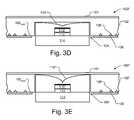
- FIG. 3Dillustrates the use of an overmolded lens 116 ′′ for re-directing the top emitted light from LED 110 ′′ into the waveguide 102 .
- FIG. 3Eis similar to FIG. 3D , with the cavity 104 ′ in the form of a through-hole extending from the bottom surface to the top surface.
- FIG. 4is a cross-sectional view of one embodiment of a low profile side-emitting LED 110 that may be used with the backlight 100 .
- the LED 110includes a semiconductor light emitting element 132 , a wavelength converting element 134 , and a reflective film 136 .
- the side emitting LED 110is mounted on a submount 112 , which is mounted on a printed circuit board 114 .
- Other embodiments of thin, side-emitting LEDs that may be used in the backlight embodimentscan be found in U.S. application Ser. No. 11/423,419, entitled Low Profile Side Emitting LED, filed Jun. 9, 2006, by Oleg Shchekin et al., assigned to the present assignee, and incorporated herein by reference.
- the active layer of the LED 110in one example generates blue light.
- the LED 110is formed on a starting growth substrate, such as sapphire, SiC, or GaN.
- a starting growth substratesuch as sapphire, SiC, or GaN.
- an n-layer 132 nis grown followed by an active layer 132 active , followed by a p-layer 132 p .
- the p-layer 132 pis etched to expose a portion of the underlying n-layer 132 n .
- Reflective metal electrodes 140e.g., silver, aluminum, or an alloy
- the active layer 132 activeemits light whose wavelength is determined by the composition of the active layer (e.g., AlInGaN).
- LEDsare well known and need not be described in further detail. Additional detail of forming LEDs is described in U.S. Pat. No. 6,828,596 to Steigerwald et al. and U.S. Pat. No. 6,876,008 to Bhat et al., both assigned to the present assignee and incorporated herein by reference.
- the semiconductor light emitting element 132is then mounted on a submount 112 as a flip chip.
- the submount 112contains metal electrodes 142 that are soldered or ultrasonically welded to the metal 140 via solder balls 144 . Other types of bonding can also be used.
- the solder balls 144may be deleted if the electrodes themselves can be ultrasonically welded together.
- the submount electrodes 142are electrically connected by vias to pads on the bottom of the submount 112 so the submount 112 can be surface mounted to metal pads on a printed circuit board 114 .
- Metal traces on the circuit board 114electrically coupled the pads to a power supply.
- the submount 112may be formed of any suitable material, such as alumina nitride, ceramic, silicon, alumina, etc. If the submount material is conductive, an insulating layer is formed over the substrate material, and the metal electrode pattern is formed over the insulating layer.
- the submount 112acts as a mechanical support, provides an electrical interface between the delicate n and p electrodes on the LED chip and a power supply, and provides heat sinking. Submounts are well known. Processing of the LED semiconductor layers may occur before or after the LED is mounted on the submount 112 .
- the growth substrateis removed, such as by CMP or using a laser lift-off method, where a laser heats the interface of the GaN and growth substrate to create a high-pressure gas that pushes the substrate away from the GaN.
- removal of the growth substrateis performed after an array of LEDs is mounted on a submount wafer and prior to the LEDs/submounts being singulated (e.g., by sawing).
- a wavelength converting element 134such as planar phosphor layer 134 is positioned over the top of the LED for wavelength-converting the blue light emitted from the active layer 132 active .
- the element 134may be a transparent element, such as glass, that may be positioned over the top of the LED when a blue-side emitter is desired.
- the phosphor layer 134may be preformed as a ceramic sheet and affixed to the LED layers, or the phosphor particles may be thin-film deposited, such as by electrophoresis.
- the phosphor ceramic sheetmay be sintered phosphor particles or phosphor particles in a transparent or translucent binder, which may be organic or inorganic.
- the light emitted by the phosphor layer 134when mixed with blue light, creates white light or another desired color.
- the color temperature of the white lightdepends largely on the Ce doping in the phosphor as well as the thickness of the phosphor layer 134 .
- a reflective film 136is then formed over the transparent or phosphor layer 134 .
- the reflective film 136is substantially parallel with the top surface of the semiconductor light emitting element 132 .
- the reflective film 136may be specular or diffusing.
- a specular reflectormay be a distributed Bragg reflector (DBR) formed of organic or inorganic layers.
- the specular reflectormay also be a layer of aluminum or other reflective metal, or a combination of DBR and metal.
- a diffusing reflectormay be formed of a metal deposited on a roughened surface or a diffusing material such as a suitable white paint or a sol-gel solution with TiO2 in, e.g., silicone, solgel or silres.
- the phosphor layer 134also helps to diffuse the light to improve light extraction efficiency.
- the reflector 136is spaced away from the LED, such as a reflector supported by the waveguide 102 in the cavity 104 over the active layer, resulting in the LED still being a side-emitting LED since little (e.g., up to 10%) direct light exits the backlight above the LED.
- blue LEDscan be used in combination with a remote phosphor layer elsewhere in the backlight.
- the active layer 132 activeMost light emitted by the active layer 132 active is either directly emitted through the sides of the LED, or emitted through the sides after one or more internal reflections. If the top reflector 136 is very thin, some light may leak through the top reflector 136 .
- the submount 112has a thickness of about 380 microns
- the semiconductor layershave a combined thickness of about 5 microns
- the phosphor layer 134has a thickness of about 200 microns
- the reflective film 136has a thickness of about 150 microns, so that the LED plus the submount is less than 1 mm thick.
- the LED 110can be made thicker.
- the length of each side of the LEDis typically less than 1 mm, for example, the length of a side may be 0.6 mm, however, a side length of 1.0 mm may be used, e.g., for higher power applications. Greater heights may be used in case of other side emitting configuration, such as overmolded optics on top emitters or external optical components for side re-direction.
- the overmolded lens 116is a collimating optic coupled to the LED 110 that collimates the side emitted light in the horizontal plane.
- the lens 116may have different configurations, as illustrated in FIGS. 5A and 5B which illustrate top plan views of a square and circular configuration of the lens 116 with the LED 110 . If desired, different configurations of the lens 116 may be used at different locations within the backlight 100 . As can be seen, the lens 116 is coupled to each light emitting side of the LED 110 , and thus, in the present embodiment where the LED 110 has four light emitting sides, the lens 116 includes four entrance surfaces coupled to each side. If desired, separate individual lenses may be combined to form a single lens 116 . Additionally, different configurations of lenses may be used with top emitting LEDs.
- FIG. 6illustrates a top plan view of the LED 110 with a portion of the lens 116 , wherein the entrance surface of the lens 116 have vertically oriented angled walls 117 , which may also be used to improve the angular mixing of the light within the lens 116 .
- the varying angles of the walls 117 of the entrance surface of the lens 116refract the light emitted by the LED 110 at different angles so the light is spread more evenly. Because the light is being collimated in the horizontal plane, there is no need to produce horizontally oriented angled walls.
- FIG. 6illustrates walls 117 with a saw-tooth configuration, other configurations may be used, such as rounded or scallop shapes.
- the shape of the sidewallsmay also be varied based on the distribution of the extraction features formed on the bottom surface of the waveguide to achieve the most uniform brightness profile at the light output of the backlight.
- the lens 116may be produced by overmolding and in one embodiment, a molded lead frame is used to form the bottom of the lens 116 .
- FIG. 7illustrates an LED 110 with an overmolded lens 116 formed on a molded lead frame 150 .
- the molded lead frame 150may be produced from a patterned conductor material with a plastic or other appropriate material injection molded around the conductor material. The injection molded material is molded to form the bottom surface of the lens 116 and may be coated with a reflective layer 152 , such as aluminum or silver.
- the LED 110can then be mounted on the lead frame 150 and silicone or other appropriate material is deposited and molded to form the lens 116 .
- a reflective layer 154e.g., aluminum or silver, can then be deposited over the top surface of the lens 116 .
- No reflective coatingis necessary or used if the lens 116 design is based on total internal reflection within the lens material.
- a double overmolding processmay be used, in which a first material (illustrated with broken lines 156 ) with a first refractive index, e.g., 1.6, is deposited and molded. Additional material, with a different refractive index, e.g., 1.3, is then deposited and molded to form the remainder of the lens 116 .
- both the first material and the second materialmay be silicone with different refractive indices.
- the refractive indicesmay be selected so that desired refraction occurs at the index step to achieve angular mixing of the light.
- features, such as those shown in FIG. 6may be molded in the first silicon material 156 to help achieve the desired angular mixing of light.
- a wavelength converting element 160may be positioned on the front surface 102 front of the waveguide, as illustrated in FIG. 8 .
- the LED 110 ′which may be a top emitter or side emitter, does not include a wavelength converting element, but instead produces blue light that is converted by the wavelength converting element 160 as the light exits the waveguide 102 .
- FIGS. 9A and 9Billustrate a top view and a side view of another embodiment of a waveguide 200 .
- two thin waveguides 202 and 204are used with LEDs 110 (shown in FIG. 9B ) and mirrors 206 208 along one edge 203 and 205 , respectively.
- the LEDs 110are distributed behind the backlight as illustrated in, e.g., FIG. 3A , 3 B, or 3 C and do not extend into any bezel region, e.g., between the waveguides 202 and 204 .
- the edges 203 and 205 of the waveguides 202 and 204are positioned adjacent each other. As illustrated in FIG.
- the two waveguides 202 and 204are configured in a “V” shape so that the adjacent edges 203 and 205 are farther from the LCD screen 210 then the outside edges 207 and 209 , to produce an LCD screen 210 with little or no bezel.
Landscapes
- Physics & Mathematics (AREA)
- General Physics & Mathematics (AREA)
- Optics & Photonics (AREA)
- Nonlinear Science (AREA)
- Engineering & Computer Science (AREA)
- Microelectronics & Electronic Packaging (AREA)
- Mathematical Physics (AREA)
- Chemical & Material Sciences (AREA)
- Crystallography & Structural Chemistry (AREA)
- Planar Illumination Modules (AREA)
- Led Device Packages (AREA)
- Liquid Crystal (AREA)
Abstract
Description
Claims (18)
Priority Applications (11)
| Application Number | Priority Date | Filing Date | Title |
|---|---|---|---|
| US12/236,542US8755005B2 (en) | 2008-09-24 | 2008-09-24 | Thin edge backlight with LEDS optically coupled to the back surface |
| PCT/IB2009/054132WO2010035209A1 (en) | 2008-09-24 | 2009-09-21 | Thin edge backlight with leds optically coupled to the back surface |
| EP09787263AEP2342594A1 (en) | 2008-09-24 | 2009-09-21 | Thin edge backlight with leds optically coupled to the back surface |
| KR1020117009195AKR20110063682A (en) | 2008-09-24 | 2009-09-21 | Thin edge backlight with LEDs optically connected to the back |
| TW098131836ATWI502253B (en) | 2008-09-24 | 2009-09-21 | Thin edge backlight with leds optically coupled to the back surface |
| CN2009801374682ACN102165344A (en) | 2008-09-24 | 2009-09-21 | Thin edge backlight with LEDs optically coupled to the back surface |
| BRPI0913751ABRPI0913751A2 (en) | 2008-09-24 | 2009-09-21 | apparatus comprising a plurality of LEDs and apparatus comprising a first plurality of light emitting diodes |
| CN201510048177.3ACN104656182B (en) | 2008-09-24 | 2009-09-21 | Thin edges backlight with the LED for being optically coupled to rear surface |
| JP2011527458AJP2012503782A (en) | 2008-09-24 | 2009-09-21 | Thin edge backlight with LEDs optically coupled to the back surface |
| RU2011116089/28ARU2525694C2 (en) | 2008-09-24 | 2009-09-21 | Thin edge backlight assembly with leds optically connected to back surface |
| JP2015002200AJP5936158B2 (en) | 2008-09-24 | 2015-01-08 | Thin edge backlight with LEDs optically coupled to the back surface |
Applications Claiming Priority (1)
| Application Number | Priority Date | Filing Date | Title |
|---|---|---|---|
| US12/236,542US8755005B2 (en) | 2008-09-24 | 2008-09-24 | Thin edge backlight with LEDS optically coupled to the back surface |
Publications (2)
| Publication Number | Publication Date |
|---|---|
| US20100073597A1 US20100073597A1 (en) | 2010-03-25 |
| US8755005B2true US8755005B2 (en) | 2014-06-17 |
Family
ID=41445624
Family Applications (1)
| Application Number | Title | Priority Date | Filing Date |
|---|---|---|---|
| US12/236,542Expired - Fee RelatedUS8755005B2 (en) | 2008-09-24 | 2008-09-24 | Thin edge backlight with LEDS optically coupled to the back surface |
Country Status (9)
| Country | Link |
|---|---|
| US (1) | US8755005B2 (en) |
| EP (1) | EP2342594A1 (en) |
| JP (2) | JP2012503782A (en) |
| KR (1) | KR20110063682A (en) |
| CN (2) | CN102165344A (en) |
| BR (1) | BRPI0913751A2 (en) |
| RU (1) | RU2525694C2 (en) |
| TW (1) | TWI502253B (en) |
| WO (1) | WO2010035209A1 (en) |
Cited By (23)
| Publication number | Priority date | Publication date | Assignee | Title |
|---|---|---|---|---|
| US20130215640A1 (en)* | 2012-02-21 | 2013-08-22 | Hon Hai Precision Industry Co., Ltd. | Light guide plate and method of manufacturing same |
| US20140355302A1 (en)* | 2013-03-15 | 2014-12-04 | Cree, Inc. | Outdoor and/or Enclosed Structure LED Luminaire for General Illumination Applications, Such as Parking Lots and Structures |
| US9291320B2 (en) | 2013-01-30 | 2016-03-22 | Cree, Inc. | Consolidated troffer |
| WO2016048971A1 (en) | 2014-09-23 | 2016-03-31 | Koninklijke Philips N.V. | Luminance pattern shaping using a back-emitting led and a reflective substrate |
| US9366396B2 (en) | 2013-01-30 | 2016-06-14 | Cree, Inc. | Optical waveguide and lamp including same |
| US9366799B2 (en) | 2013-03-15 | 2016-06-14 | Cree, Inc. | Optical waveguide bodies and luminaires utilizing same |
| US9389367B2 (en) | 2013-01-30 | 2016-07-12 | Cree, Inc. | Optical waveguide and luminaire incorporating same |
| US9411086B2 (en) | 2013-01-30 | 2016-08-09 | Cree, Inc. | Optical waveguide assembly and light engine including same |
| US9442243B2 (en) | 2013-01-30 | 2016-09-13 | Cree, Inc. | Waveguide bodies including redirection features and methods of producing same |
| US20170090101A1 (en)* | 2015-09-30 | 2017-03-30 | Nichia Corporation | Lighting device and method for manufacturing the same |
| US9625638B2 (en) | 2013-03-15 | 2017-04-18 | Cree, Inc. | Optical waveguide body |
| US9690029B2 (en) | 2013-01-30 | 2017-06-27 | Cree, Inc. | Optical waveguides and luminaires incorporating same |
| US9798072B2 (en) | 2013-03-15 | 2017-10-24 | Cree, Inc. | Optical element and method of forming an optical element |
| US9869432B2 (en) | 2013-01-30 | 2018-01-16 | Cree, Inc. | Luminaires using waveguide bodies and optical elements |
| US9920901B2 (en) | 2013-03-15 | 2018-03-20 | Cree, Inc. | LED lensing arrangement |
| US10209429B2 (en) | 2013-03-15 | 2019-02-19 | Cree, Inc. | Luminaire with selectable luminous intensity pattern |
| US10416377B2 (en) | 2016-05-06 | 2019-09-17 | Cree, Inc. | Luminaire with controllable light emission |
| US10436970B2 (en) | 2013-03-15 | 2019-10-08 | Ideal Industries Lighting Llc | Shaped optical waveguide bodies |
| US10502899B2 (en)* | 2013-03-15 | 2019-12-10 | Ideal Industries Lighting Llc | Outdoor and/or enclosed structure LED luminaire |
| US20200159069A1 (en)* | 2016-12-28 | 2020-05-21 | Rohinni, LLC | Backlighting display apparatus |
| US10677980B2 (en) | 2016-09-12 | 2020-06-09 | Lumileds Llc | Interconnectable light guide tiles |
| US11112083B2 (en) | 2013-03-15 | 2021-09-07 | Ideal Industries Lighting Llc | Optic member for an LED light fixture |
| US11719882B2 (en) | 2016-05-06 | 2023-08-08 | Ideal Industries Lighting Llc | Waveguide-based light sources with dynamic beam shaping |
Families Citing this family (34)
| Publication number | Priority date | Publication date | Assignee | Title |
|---|---|---|---|---|
| US20100231823A1 (en)* | 2008-12-26 | 2010-09-16 | Dai Nippon Printing Co., Ltd. | Optical sheet, surface light source device, and display device |
| EP2449414A1 (en)* | 2009-06-29 | 2012-05-09 | 3M Innovative Properties Company | Lightguide and light source incorporating same |
| US9097826B2 (en)* | 2011-10-08 | 2015-08-04 | Svv Technology Innovations, Inc. | Collimating illumination systems employing a waveguide |
| DE102012102114B4 (en)* | 2012-03-13 | 2021-09-16 | OSRAM Opto Semiconductors Gesellschaft mit beschränkter Haftung | Radiation-emitting semiconductor component, lighting device and display device |
| RU2657466C2 (en)* | 2012-12-18 | 2018-06-14 | Филипс Лайтинг Холдинг Б.В. | Lighting strip, lighting system, panel support element and modular panel system |
| US9952372B2 (en)* | 2013-03-15 | 2018-04-24 | Cree, Inc. | Luminaire utilizing waveguide |
| CN103557445A (en)* | 2013-08-26 | 2014-02-05 | 中国科学院苏州纳米技术与纳米仿生研究所 | Side-emission semiconductor light-emitting device, backlight module and area light source |
| JP2016531450A (en) | 2013-09-23 | 2016-10-06 | グロ アーベーGlo Ab | Integrated backlight unit |
| WO2015064883A1 (en)* | 2013-11-01 | 2015-05-07 | Seoul Semiconductor Co., Ltd. | Light source module and backlight unit having the same |
| US9720163B2 (en) | 2013-12-09 | 2017-08-01 | Glo Ab | Optical display system |
| US12372219B2 (en)* | 2014-05-30 | 2025-07-29 | Cree Lighting Usa Llc | LED luminaire with a cavity, finned interior, and a curved outer wall extending from a surface on which the light source is mounted |
| DE102015100250A1 (en)* | 2015-01-09 | 2016-07-14 | Osram Oled Gmbh | Light emitting device |
| US10222543B2 (en)* | 2015-03-16 | 2019-03-05 | Sharp Kabushiki Kaisha | Lighting device, display device, and television device |
| US9633883B2 (en) | 2015-03-20 | 2017-04-25 | Rohinni, LLC | Apparatus for transfer of semiconductor devices |
| JP6506899B2 (en)* | 2015-10-08 | 2019-04-24 | 日亜化学工業株式会社 | Light emitting device, integrated light emitting device and light emitting module |
| WO2017061127A1 (en) | 2015-10-08 | 2017-04-13 | Nichia Corporation | Light-emitting device, integrated light-emitting device, and light-emitting module |
| WO2017184941A1 (en) | 2016-04-22 | 2017-10-26 | Neil Deeman | Small pitch direct view display and method of making thereof |
| US10141215B2 (en) | 2016-11-03 | 2018-11-27 | Rohinni, LLC | Compliant needle for direct transfer of semiconductor devices |
| US10471545B2 (en) | 2016-11-23 | 2019-11-12 | Rohinni, LLC | Top-side laser for direct transfer of semiconductor devices |
| US10504767B2 (en) | 2016-11-23 | 2019-12-10 | Rohinni, LLC | Direct transfer apparatus for a pattern array of semiconductor device die |
| US10062588B2 (en) | 2017-01-18 | 2018-08-28 | Rohinni, LLC | Flexible support substrate for transfer of semiconductor devices |
| FR3064531B1 (en)* | 2017-03-31 | 2019-04-05 | Saint-Gobain Glass France | GLAZING LIGHTING. |
| KR102293607B1 (en)* | 2017-06-07 | 2021-08-26 | 삼성전자주식회사 | Display apparatus |
| WO2019183016A1 (en)* | 2018-03-22 | 2019-09-26 | Corning Incorporated | Illumination devices including light guide plates |
| WO2019201729A1 (en)* | 2018-04-18 | 2019-10-24 | Lumileds Holding B.V. | Segmented backlight structure with in-coupling structures |
| CN113168815B (en)* | 2018-04-18 | 2022-12-30 | 亮锐有限责任公司 | LED backlight system |
| US10410905B1 (en) | 2018-05-12 | 2019-09-10 | Rohinni, LLC | Method and apparatus for direct transfer of multiple semiconductor devices |
| JP6912730B2 (en)* | 2018-07-09 | 2021-08-04 | 日亜化学工業株式会社 | Manufacturing method of light emitting module |
| JP6729646B2 (en)* | 2018-08-21 | 2020-07-22 | 日亜化学工業株式会社 | Light emitting device |
| US11094571B2 (en) | 2018-09-28 | 2021-08-17 | Rohinni, LLC | Apparatus to increase transferspeed of semiconductor devices with micro-adjustment |
| KR102785601B1 (en)* | 2018-12-26 | 2025-03-26 | 엘지이노텍 주식회사 | Lighting module, lighting apparatus and manufacturing method thereof |
| US20230161127A1 (en)* | 2020-04-15 | 2023-05-25 | CommScope Connectivity Belgium BV | Device and method for sealing cables in telecommunications enclosures |
| KR102607878B1 (en)* | 2021-09-17 | 2023-11-30 | 현대모비스 주식회사 | Led module and car including the same |
| KR20230143435A (en)* | 2022-04-05 | 2023-10-12 | 삼성전자주식회사 | Display apparatus |
Citations (13)
| Publication number | Priority date | Publication date | Assignee | Title |
|---|---|---|---|---|
| US4059916A (en)* | 1975-01-30 | 1977-11-29 | Copal Company Limited | Light diffusing device |
| US20050140912A1 (en)* | 1998-01-12 | 2005-06-30 | Semiconductor Energy Laboratory Co., Ltd. | Display device |
| US20060043391A1 (en)* | 2003-04-15 | 2006-03-02 | Erchak Alexei A | Light emitting devices for liquid crystal displays |
| US20060232996A1 (en)* | 2002-12-12 | 2006-10-19 | Dong-Hoon Kim | Light guide plate with stepped edge and display device having the same |
| US20070138494A1 (en)* | 2005-12-19 | 2007-06-21 | Lumileds Lighting U.S., Llc | Light-emitting device |
| US20070215890A1 (en) | 2006-03-17 | 2007-09-20 | Philips Lumileds Lighting Company, Llc | White LED for backlight with phosphor plates |
| US20070284600A1 (en) | 2006-06-09 | 2007-12-13 | Philips Lumileds Lighting Company, Llc | Low Profile Side Emitting LED |
| DE202007017224U1 (en) | 2007-12-10 | 2008-03-27 | Wll Wehrsdorfer Led-Lichttechnik Gmbh | Flat luminous element |
| US20080137004A1 (en)* | 2005-02-08 | 2008-06-12 | Fujifilm Corporation | Light Guide Plate, and Planar Lighting Device and Liquid Crystal Display Device Using Such Light Guide Plate |
| US20080198300A1 (en)* | 2007-02-21 | 2008-08-21 | Fujifilm Corporation | Liquid crystal display device |
| US20080204623A1 (en)* | 2007-02-28 | 2008-08-28 | Funai Electric Co., Ltd. | Liquid crystal display device |
| US7424197B2 (en) | 1992-03-23 | 2008-09-09 | 3M Innovative Properties Company | Luminaire device |
| US20090059579A1 (en)* | 2007-08-27 | 2009-03-05 | Jae Hong Shin | Surface light source using white light emitting diodes and liquid crystal display backlight unit having the same |
Family Cites Families (27)
| Publication number | Priority date | Publication date | Assignee | Title |
|---|---|---|---|---|
| JPS62171268A (en)* | 1986-01-23 | 1987-07-28 | Sumitomo Electric Ind Ltd | Picture input device |
| JP2521824B2 (en)* | 1989-12-22 | 1996-08-07 | 株式会社エンプラス | Lighting equipment |
| JPH04338723A (en)* | 1991-05-16 | 1992-11-26 | Seiko Epson Corp | Display backlight source device and liquid crystal display device |
| JPH0555567U (en)* | 1991-12-24 | 1993-07-23 | スタンレー電気株式会社 | LED surface light source device |
| JPH08254963A (en)* | 1995-03-16 | 1996-10-01 | Hayashi Telempu Co Ltd | Display panel for in-vehicle equipment |
| JPH1082916A (en)* | 1996-09-06 | 1998-03-31 | Omron Corp | Surface light source device and liquid crystal display device |
| JP3427636B2 (en)* | 1996-09-06 | 2003-07-22 | オムロン株式会社 | Surface light source device and liquid crystal display device |
| JPH10104623A (en)* | 1996-09-30 | 1998-04-24 | Taihei Meiban Kogyosho:Kk | Back light body for liquid crystal |
| JP2001125497A (en)* | 1999-10-25 | 2001-05-11 | Shokosha:Kk | Illumination device and liquid crystal display device having the illumination device |
| DE10102586A1 (en)* | 2001-01-20 | 2002-07-25 | Philips Corp Intellectual Pty | Luminair with light emission surface and punctiform light sources |
| CN1182428C (en)* | 2001-07-04 | 2004-12-29 | 刘保伸 | Combination device of illuminant and light guide plate for backlight assembly |
| US6802628B2 (en)* | 2002-10-18 | 2004-10-12 | Heng Huang Kuo | Vertically downward type back-light module |
| JP2004171803A (en)* | 2002-11-18 | 2004-06-17 | Asahi Techno Kk | Surface light emitting device |
| JP2004302067A (en)* | 2003-03-31 | 2004-10-28 | Toyota Industries Corp | Light guide plate, lighting device, and liquid crystal display device |
| JP2005203225A (en)* | 2004-01-15 | 2005-07-28 | Nippon Leiz Co Ltd | Light guide body and plane light emitting device |
| JP4535792B2 (en)* | 2004-07-01 | 2010-09-01 | Nec液晶テクノロジー株式会社 | Backlight and liquid crystal display device including the backlight |
| JP4760048B2 (en)* | 2005-02-18 | 2011-08-31 | ソニー株式会社 | Backlight device and liquid crystal display device |
| JP2006236770A (en)* | 2005-02-24 | 2006-09-07 | Sony Corp | Backlight device and liquid crystal display |
| JP2006313682A (en)* | 2005-05-09 | 2006-11-16 | Toyoda Gosei Co Ltd | Light source unit and light source device equipped with this |
| JP4430585B2 (en)* | 2005-06-16 | 2010-03-10 | 三菱レイヨン株式会社 | Surface light source device |
| JP2007141546A (en)* | 2005-11-16 | 2007-06-07 | Radiant Opt-Electronics Corp | Light mixing plate and direct backlight using the light mixing plate |
| JP4600257B2 (en)* | 2005-11-25 | 2010-12-15 | ソニー株式会社 | Light guide plate, backlight device, manufacturing method thereof, and liquid crystal display device |
| JP4541346B2 (en)* | 2005-11-30 | 2010-09-08 | 昭和電工株式会社 | Surface light source device |
| US7909496B2 (en)* | 2006-02-01 | 2011-03-22 | Koninklijke Philips Electronics N.V. | Lighting system for creating an illuminated surface |
| JP2008059786A (en)* | 2006-08-29 | 2008-03-13 | Seiko Instruments Inc | Lighting apparatus and display device provided with the same |
| DE602007013865D1 (en)* | 2007-02-14 | 2011-05-26 | Chi Lin Technology Jen Te Hsiang | Light mixer and backlight module with it |
| EP2269102A1 (en)* | 2008-04-08 | 2011-01-05 | Koninklijke Philips Electronics N.V. | Illumination system, backlighting system and display device |
- 2008
- 2008-09-24USUS12/236,542patent/US8755005B2/ennot_activeExpired - Fee Related
- 2009
- 2009-09-21JPJP2011527458Apatent/JP2012503782A/enactivePending
- 2009-09-21EPEP09787263Apatent/EP2342594A1/ennot_activeWithdrawn
- 2009-09-21KRKR1020117009195Apatent/KR20110063682A/ennot_activeCeased
- 2009-09-21TWTW098131836Apatent/TWI502253B/ennot_activeIP Right Cessation
- 2009-09-21CNCN2009801374682Apatent/CN102165344A/enactivePending
- 2009-09-21CNCN201510048177.3Apatent/CN104656182B/ennot_activeExpired - Fee Related
- 2009-09-21BRBRPI0913751Apatent/BRPI0913751A2/ennot_activeIP Right Cessation
- 2009-09-21WOPCT/IB2009/054132patent/WO2010035209A1/enactiveApplication Filing
- 2009-09-21RURU2011116089/28Apatent/RU2525694C2/ennot_activeIP Right Cessation
- 2015
- 2015-01-08JPJP2015002200Apatent/JP5936158B2/ennot_activeExpired - Fee Related
Patent Citations (13)
| Publication number | Priority date | Publication date | Assignee | Title |
|---|---|---|---|---|
| US4059916A (en)* | 1975-01-30 | 1977-11-29 | Copal Company Limited | Light diffusing device |
| US7424197B2 (en) | 1992-03-23 | 2008-09-09 | 3M Innovative Properties Company | Luminaire device |
| US20050140912A1 (en)* | 1998-01-12 | 2005-06-30 | Semiconductor Energy Laboratory Co., Ltd. | Display device |
| US20060232996A1 (en)* | 2002-12-12 | 2006-10-19 | Dong-Hoon Kim | Light guide plate with stepped edge and display device having the same |
| US20060043391A1 (en)* | 2003-04-15 | 2006-03-02 | Erchak Alexei A | Light emitting devices for liquid crystal displays |
| US20080137004A1 (en)* | 2005-02-08 | 2008-06-12 | Fujifilm Corporation | Light Guide Plate, and Planar Lighting Device and Liquid Crystal Display Device Using Such Light Guide Plate |
| US20070138494A1 (en)* | 2005-12-19 | 2007-06-21 | Lumileds Lighting U.S., Llc | Light-emitting device |
| US20070215890A1 (en) | 2006-03-17 | 2007-09-20 | Philips Lumileds Lighting Company, Llc | White LED for backlight with phosphor plates |
| US20070284600A1 (en) | 2006-06-09 | 2007-12-13 | Philips Lumileds Lighting Company, Llc | Low Profile Side Emitting LED |
| US20080198300A1 (en)* | 2007-02-21 | 2008-08-21 | Fujifilm Corporation | Liquid crystal display device |
| US20080204623A1 (en)* | 2007-02-28 | 2008-08-28 | Funai Electric Co., Ltd. | Liquid crystal display device |
| US20090059579A1 (en)* | 2007-08-27 | 2009-03-05 | Jae Hong Shin | Surface light source using white light emitting diodes and liquid crystal display backlight unit having the same |
| DE202007017224U1 (en) | 2007-12-10 | 2008-03-27 | Wll Wehrsdorfer Led-Lichttechnik Gmbh | Flat luminous element |
Non-Patent Citations (2)
| Title |
|---|
| Gerard Harbers et al: "Performance of High Power Light Emitting Diodes in Display Illumination Applications" Journal of Display Technology, IEEE Service Center, New York, NY, US, vol. 3, No. 2, Jun. 1, 2007; p. 98-109, ,XP01182138; ISSN: 1551-319K. |
| International Search Report PCT/IB2009/054132. Attached. |
Cited By (37)
| Publication number | Priority date | Publication date | Assignee | Title |
|---|---|---|---|---|
| US20130215640A1 (en)* | 2012-02-21 | 2013-08-22 | Hon Hai Precision Industry Co., Ltd. | Light guide plate and method of manufacturing same |
| US9389367B2 (en) | 2013-01-30 | 2016-07-12 | Cree, Inc. | Optical waveguide and luminaire incorporating same |
| US9690029B2 (en) | 2013-01-30 | 2017-06-27 | Cree, Inc. | Optical waveguides and luminaires incorporating same |
| US10436969B2 (en) | 2013-01-30 | 2019-10-08 | Ideal Industries Lighting Llc | Optical waveguide and luminaire incorporating same |
| US9366396B2 (en) | 2013-01-30 | 2016-06-14 | Cree, Inc. | Optical waveguide and lamp including same |
| US11644157B2 (en) | 2013-01-30 | 2023-05-09 | Ideal Industries Lighting Llc | Luminaires using waveguide bodies and optical elements |
| US9869432B2 (en) | 2013-01-30 | 2018-01-16 | Cree, Inc. | Luminaires using waveguide bodies and optical elements |
| US9823408B2 (en) | 2013-01-30 | 2017-11-21 | Cree, Inc. | Optical waveguide and luminaire incorporating same |
| US9442243B2 (en) | 2013-01-30 | 2016-09-13 | Cree, Inc. | Waveguide bodies including redirection features and methods of producing same |
| US9519095B2 (en) | 2013-01-30 | 2016-12-13 | Cree, Inc. | Optical waveguides |
| US9581751B2 (en) | 2013-01-30 | 2017-02-28 | Cree, Inc. | Optical waveguide and lamp including same |
| US9291320B2 (en) | 2013-01-30 | 2016-03-22 | Cree, Inc. | Consolidated troffer |
| US9411086B2 (en) | 2013-01-30 | 2016-08-09 | Cree, Inc. | Optical waveguide assembly and light engine including same |
| US9920901B2 (en) | 2013-03-15 | 2018-03-20 | Cree, Inc. | LED lensing arrangement |
| US9798072B2 (en) | 2013-03-15 | 2017-10-24 | Cree, Inc. | Optical element and method of forming an optical element |
| US9625638B2 (en) | 2013-03-15 | 2017-04-18 | Cree, Inc. | Optical waveguide body |
| US10502899B2 (en)* | 2013-03-15 | 2019-12-10 | Ideal Industries Lighting Llc | Outdoor and/or enclosed structure LED luminaire |
| US9366799B2 (en) | 2013-03-15 | 2016-06-14 | Cree, Inc. | Optical waveguide bodies and luminaires utilizing same |
| US20140355302A1 (en)* | 2013-03-15 | 2014-12-04 | Cree, Inc. | Outdoor and/or Enclosed Structure LED Luminaire for General Illumination Applications, Such as Parking Lots and Structures |
| US10209429B2 (en) | 2013-03-15 | 2019-02-19 | Cree, Inc. | Luminaire with selectable luminous intensity pattern |
| US10379278B2 (en)* | 2013-03-15 | 2019-08-13 | Ideal Industries Lighting Llc | Outdoor and/or enclosed structure LED luminaire outdoor and/or enclosed structure LED luminaire having outward illumination |
| US11112083B2 (en) | 2013-03-15 | 2021-09-07 | Ideal Industries Lighting Llc | Optic member for an LED light fixture |
| US10436970B2 (en) | 2013-03-15 | 2019-10-08 | Ideal Industries Lighting Llc | Shaped optical waveguide bodies |
| US10193035B2 (en) | 2014-09-23 | 2019-01-29 | Lumileds Llc | Luminance pattern shaping using a back-emitting LED and a reflective substrate |
| WO2016048971A1 (en) | 2014-09-23 | 2016-03-31 | Koninklijke Philips N.V. | Luminance pattern shaping using a back-emitting led and a reflective substrate |
| US10001594B2 (en)* | 2015-09-30 | 2018-06-19 | Nichia Corporation | Lighting device and method for manufacturing the same |
| US20170090101A1 (en)* | 2015-09-30 | 2017-03-30 | Nichia Corporation | Lighting device and method for manufacturing the same |
| US10527785B2 (en) | 2016-05-06 | 2020-01-07 | Ideal Industries Lighting Llc | Waveguide-based light sources with dynamic beam shaping |
| US10890714B2 (en) | 2016-05-06 | 2021-01-12 | Ideal Industries Lighting Llc | Waveguide-based light sources with dynamic beam shaping |
| US10416377B2 (en) | 2016-05-06 | 2019-09-17 | Cree, Inc. | Luminaire with controllable light emission |
| US11372156B2 (en) | 2016-05-06 | 2022-06-28 | Ideal Industries Lighting Llc | Waveguide-based light sources with dynamic beam shaping |
| US11719882B2 (en) | 2016-05-06 | 2023-08-08 | Ideal Industries Lighting Llc | Waveguide-based light sources with dynamic beam shaping |
| US12353005B2 (en) | 2016-05-06 | 2025-07-08 | Cree Lighting Usa Llc | Waveguide-based light sources with dynamic beam shaping |
| US10677980B2 (en) | 2016-09-12 | 2020-06-09 | Lumileds Llc | Interconnectable light guide tiles |
| US10901142B2 (en) | 2016-09-12 | 2021-01-26 | Lumileds Llc | Interconnectable light guide tiles with opposing curved surfaces |
| US20200159069A1 (en)* | 2016-12-28 | 2020-05-21 | Rohinni, LLC | Backlighting display apparatus |
| US10921643B2 (en)* | 2016-12-28 | 2021-02-16 | Rohinni, LLC | Backlighting display apparatus |
Also Published As
| Publication number | Publication date |
|---|---|
| CN104656182B (en) | 2017-11-21 |
| US20100073597A1 (en) | 2010-03-25 |
| KR20110063682A (en) | 2011-06-13 |
| TW201020651A (en) | 2010-06-01 |
| JP2012503782A (en) | 2012-02-09 |
| TWI502253B (en) | 2015-10-01 |
| EP2342594A1 (en) | 2011-07-13 |
| JP2015072501A (en) | 2015-04-16 |
| RU2011116089A (en) | 2012-10-27 |
| JP5936158B2 (en) | 2016-06-15 |
| CN102165344A (en) | 2011-08-24 |
| CN104656182A (en) | 2015-05-27 |
| RU2525694C2 (en) | 2014-08-20 |
| BRPI0913751A2 (en) | 2015-10-20 |
| WO2010035209A1 (en) | 2010-04-01 |
Similar Documents
| Publication | Publication Date | Title |
|---|---|---|
| US8755005B2 (en) | Thin edge backlight with LEDS optically coupled to the back surface | |
| US7652301B2 (en) | Optical element coupled to low profile side emitting LED | |
| KR101529473B1 (en) | Thin backlight using low profile side emitting leds | |
| US7626210B2 (en) | Low profile side emitting LED | |
| US8080828B2 (en) | Low profile side emitting LED with window layer and phosphor layer | |
| US20090046479A1 (en) | Thin Backlight Using Low Profile Side Emitting LED | |
| CN102378930A (en) | Backlight including semiconductor light emitting device |
Legal Events
| Date | Code | Title | Description |
|---|---|---|---|
| AS | Assignment | Owner name:KONINKLIJKE PHILIPS ELECTRONICS N V,NETHERLANDS Free format text:ASSIGNMENT OF ASSIGNORS INTEREST;ASSIGNORS:BIERHUIZEN, SERGE J.;ENG, GREGORY W.;REEL/FRAME:021576/0455 Effective date:20080829 Owner name:PHILIPS LUMILEDS LIGHTING COMPANY, LLC,CALIFORNIA Free format text:ASSIGNMENT OF ASSIGNORS INTEREST;ASSIGNORS:BIERHUIZEN, SERGE J.;ENG, GREGORY W.;REEL/FRAME:021576/0455 Effective date:20080829 Owner name:PHILIPS LUMILEDS LIGHTING COMPANY, LLC, CALIFORNIA Free format text:ASSIGNMENT OF ASSIGNORS INTEREST;ASSIGNORS:BIERHUIZEN, SERGE J.;ENG, GREGORY W.;REEL/FRAME:021576/0455 Effective date:20080829 Owner name:KONINKLIJKE PHILIPS ELECTRONICS N V, NETHERLANDS Free format text:ASSIGNMENT OF ASSIGNORS INTEREST;ASSIGNORS:BIERHUIZEN, SERGE J.;ENG, GREGORY W.;REEL/FRAME:021576/0455 Effective date:20080829 | |
| AS | Assignment | Owner name:PHILIPS LIGHTING HOLDING B.V., NETHERLANDS Free format text:ASSIGNMENT OF ASSIGNORS INTEREST;ASSIGNOR:KONINKLIJKE PHILIPS N.V.;REEL/FRAME:040060/0009 Effective date:20160607 | |
| FEPP | Fee payment procedure | Free format text:MAINTENANCE FEE REMINDER MAILED (ORIGINAL EVENT CODE: REM.) | |
| LAPS | Lapse for failure to pay maintenance fees | Free format text:PATENT EXPIRED FOR FAILURE TO PAY MAINTENANCE FEES (ORIGINAL EVENT CODE: EXP.) | |
| STCH | Information on status: patent discontinuation | Free format text:PATENT EXPIRED DUE TO NONPAYMENT OF MAINTENANCE FEES UNDER 37 CFR 1.362 | |
| FP | Lapsed due to failure to pay maintenance fee | Effective date:20180617 | |
| FP | Lapsed due to failure to pay maintenance fee | Effective date:20180617 |