US8752280B2 - Extrusion process for manufacturing a Z-directed component for a printed circuit board - Google Patents
Extrusion process for manufacturing a Z-directed component for a printed circuit boardDownload PDFInfo
- Publication number
- US8752280B2 US8752280B2US13/250,812US201113250812AUS8752280B2US 8752280 B2US8752280 B2US 8752280B2US 201113250812 AUS201113250812 AUS 201113250812AUS 8752280 B2US8752280 B2US 8752280B2
- Authority
- US
- United States
- Prior art keywords
- directed component
- component
- directed
- pcb
- conductive
- Prior art date
- Legal status (The legal status is an assumption and is not a legal conclusion. Google has not performed a legal analysis and makes no representation as to the accuracy of the status listed.)
- Active, expires
Links
- 238000000034methodMethods0.000titleclaimsabstractdescription51
- 238000004519manufacturing processMethods0.000titleclaimsabstractdescription19
- 238000001125extrusionMethods0.000titleclaimsdescription45
- 230000008569processEffects0.000titledescription25
- 239000000463materialSubstances0.000claimsabstractdescription105
- 239000000758substrateSubstances0.000claimsabstractdescription53
- 239000004020conductorSubstances0.000claimsabstractdescription51
- 238000003780insertionMethods0.000claimsabstractdescription11
- 230000037431insertionEffects0.000claimsabstractdescription11
- 238000010438heat treatmentMethods0.000claimsdescription3
- 238000010924continuous productionMethods0.000claims1
- 239000003990capacitorSubstances0.000description36
- 238000007747platingMethods0.000description34
- HHXNVASVVVNNDG-UHFFFAOYSA-N1,2,3,4,5-pentachloro-6-(2,3,6-trichlorophenyl)benzeneChemical compoundClC1=CC=C(Cl)C(C=2C(=C(Cl)C(Cl)=C(Cl)C=2Cl)Cl)=C1ClHHXNVASVVVNNDG-UHFFFAOYSA-N0.000description16
- 229920002120photoresistant polymerPolymers0.000description13
- 238000013461designMethods0.000description10
- 239000000853adhesiveSubstances0.000description8
- 230000001070adhesive effectEffects0.000description8
- 230000006870functionEffects0.000description8
- 239000012212insulatorSubstances0.000description7
- 229910000679solderInorganic materials0.000description6
- RYGMFSIKBFXOCR-UHFFFAOYSA-NCopperChemical compound[Cu]RYGMFSIKBFXOCR-UHFFFAOYSA-N0.000description5
- 230000005540biological transmissionEffects0.000description5
- 229910052802copperInorganic materials0.000description5
- 239000010949copperSubstances0.000description5
- 239000003989dielectric materialSubstances0.000description5
- 229910000859α-FeInorganic materials0.000description5
- XEEYBQQBJWHFJM-UHFFFAOYSA-NIronChemical compound[Fe]XEEYBQQBJWHFJM-UHFFFAOYSA-N0.000description4
- 239000011324beadSubstances0.000description4
- 239000000919ceramicSubstances0.000description4
- 238000010304firingMethods0.000description4
- 230000001939inductive effectEffects0.000description4
- 239000011800void materialSubstances0.000description4
- 238000010276constructionMethods0.000description3
- 230000008878couplingEffects0.000description3
- 238000010168coupling processMethods0.000description3
- 238000005859coupling reactionMethods0.000description3
- 230000007423decreaseEffects0.000description3
- 239000007788liquidSubstances0.000description3
- 230000002093peripheral effectEffects0.000description3
- 230000035699permeabilityEffects0.000description3
- 230000005855radiationEffects0.000description3
- 230000006798recombinationEffects0.000description3
- 238000005215recombinationMethods0.000description3
- OKTJSMMVPCPJKN-UHFFFAOYSA-NCarbonChemical compound[C]OKTJSMMVPCPJKN-UHFFFAOYSA-N0.000description2
- 229910052782aluminiumInorganic materials0.000description2
- XAGFODPZIPBFFR-UHFFFAOYSA-NaluminiumChemical compound[Al]XAGFODPZIPBFFR-UHFFFAOYSA-N0.000description2
- 229910002113barium titanateInorganic materials0.000description2
- 229910052799carbonInorganic materials0.000description2
- 239000011248coating agentSubstances0.000description2
- 238000000576coating methodMethods0.000description2
- 238000005868electrolysis reactionMethods0.000description2
- 239000012530fluidSubstances0.000description2
- 239000003292glueSubstances0.000description2
- 230000012447hatchingEffects0.000description2
- 229910052742ironInorganic materials0.000description2
- 239000010445micaSubstances0.000description2
- 229910052618mica groupInorganic materials0.000description2
- 238000012216screeningMethods0.000description2
- 239000004065semiconductorSubstances0.000description2
- 229910052710siliconInorganic materials0.000description2
- 239000010703siliconSubstances0.000description2
- 238000005476solderingMethods0.000description2
- RKUAZJIXKHPFRK-UHFFFAOYSA-N1,3,5-trichloro-2-(2,4-dichlorophenyl)benzeneChemical compoundClC1=CC(Cl)=CC=C1C1=C(Cl)C=C(Cl)C=C1ClRKUAZJIXKHPFRK-UHFFFAOYSA-N0.000description1
- 244000235115Alocasia x amazonicaSpecies0.000description1
- JBRZTFJDHDCESZ-UHFFFAOYSA-NAsGaChemical compound[As]#[Ga]JBRZTFJDHDCESZ-UHFFFAOYSA-N0.000description1
- 239000004593EpoxySubstances0.000description1
- 229910001218Gallium arsenideInorganic materials0.000description1
- XUIMIQQOPSSXEZ-UHFFFAOYSA-NSiliconChemical compound[Si]XUIMIQQOPSSXEZ-UHFFFAOYSA-N0.000description1
- BQCADISMDOOEFD-UHFFFAOYSA-NSilverChemical compound[Ag]BQCADISMDOOEFD-UHFFFAOYSA-N0.000description1
- ATJFFYVFTNAWJD-UHFFFAOYSA-NTinChemical compound[Sn]ATJFFYVFTNAWJD-UHFFFAOYSA-N0.000description1
- 239000003082abrasive agentSubstances0.000description1
- 239000003570airSubstances0.000description1
- 229910045601alloyInorganic materials0.000description1
- 239000000956alloySubstances0.000description1
- 230000003466anti-cipated effectEffects0.000description1
- JRPBQTZRNDNNOP-UHFFFAOYSA-Nbarium titanateChemical compound[Ba+2].[Ba+2].[O-][Ti]([O-])([O-])[O-]JRPBQTZRNDNNOP-UHFFFAOYSA-N0.000description1
- 230000008901benefitEffects0.000description1
- 239000011230binding agentSubstances0.000description1
- 230000037237body shapeEffects0.000description1
- 239000013590bulk materialSubstances0.000description1
- 230000008859changeEffects0.000description1
- 238000007796conventional methodMethods0.000description1
- 238000005520cutting processMethods0.000description1
- 230000003247decreasing effectEffects0.000description1
- 238000009826distributionMethods0.000description1
- 238000005553drillingMethods0.000description1
- 230000005684electric fieldEffects0.000description1
- 230000008713feedback mechanismEffects0.000description1
- 101150079361fet5 geneProteins0.000description1
- 239000011152fibreglassSubstances0.000description1
- 230000005669field effectEffects0.000description1
- 229910052732germaniumInorganic materials0.000description1
- GNPVGFCGXDBREM-UHFFFAOYSA-Ngermanium atomChemical compound[Ge]GNPVGFCGXDBREM-UHFFFAOYSA-N0.000description1
- 239000011521glassSubstances0.000description1
- PCHJSUWPFVWCPO-UHFFFAOYSA-NgoldChemical compound[Au]PCHJSUWPFVWCPO-UHFFFAOYSA-N0.000description1
- 229910052737goldInorganic materials0.000description1
- 239000010931goldSubstances0.000description1
- 238000000886hydrostatic extrusionMethods0.000description1
- 239000012535impuritySubstances0.000description1
- UGKDIUIOSMUOAW-UHFFFAOYSA-Niron nickelChemical compound[Fe].[Ni]UGKDIUIOSMUOAW-UHFFFAOYSA-N0.000description1
- 230000001788irregularEffects0.000description1
- 238000003698laser cuttingMethods0.000description1
- WJZHMLNIAZSFDO-UHFFFAOYSA-Nmanganese zincChemical compound[Mn].[Zn]WJZHMLNIAZSFDO-UHFFFAOYSA-N0.000description1
- 230000007246mechanismEffects0.000description1
- 230000005012migrationEffects0.000description1
- 238000013508migrationMethods0.000description1
- 238000012986modificationMethods0.000description1
- 230000004048modificationEffects0.000description1
- 229910001120nichromeInorganic materials0.000description1
- QELJHCBNGDEXLD-UHFFFAOYSA-Nnickel zincChemical compound[Ni].[Zn]QELJHCBNGDEXLD-UHFFFAOYSA-N0.000description1
- 239000012811non-conductive materialSubstances0.000description1
- 238000010422paintingMethods0.000description1
- 229920001568phenolic resinPolymers0.000description1
- 239000004033plasticSubstances0.000description1
- 150000003071polychlorinated biphenylsChemical class0.000description1
- 229920000642polymerPolymers0.000description1
- 238000003825pressingMethods0.000description1
- 230000009467reductionEffects0.000description1
- 230000000452restraining effectEffects0.000description1
- 230000011664signalingEffects0.000description1
- 229910052709silverInorganic materials0.000description1
- 239000004332silverSubstances0.000description1
- 239000007787solidSubstances0.000description1
- 238000004528spin coatingMethods0.000description1
- 229910052715tantalumInorganic materials0.000description1
- GUVRBAGPIYLISA-UHFFFAOYSA-Ntantalum atomChemical compound[Ta]GUVRBAGPIYLISA-UHFFFAOYSA-N0.000description1
- 229910052718tinInorganic materials0.000description1
- XOLBLPGZBRYERU-UHFFFAOYSA-Ntin dioxideChemical compoundO=[Sn]=OXOLBLPGZBRYERU-UHFFFAOYSA-N0.000description1
- 229910001887tin oxideInorganic materials0.000description1
- 230000007704transitionEffects0.000description1
- 238000011144upstream manufacturingMethods0.000description1
- 230000000007visual effectEffects0.000description1
Images


Classifications
- H—ELECTRICITY
- H05—ELECTRIC TECHNIQUES NOT OTHERWISE PROVIDED FOR
- H05K—PRINTED CIRCUITS; CASINGS OR CONSTRUCTIONAL DETAILS OF ELECTRIC APPARATUS; MANUFACTURE OF ASSEMBLAGES OF ELECTRICAL COMPONENTS
- H05K1/00—Printed circuits
- H05K1/18—Printed circuits structurally associated with non-printed electric components
- H05K1/182—Printed circuits structurally associated with non-printed electric components associated with components mounted in the printed circuit board, e.g. insert mounted components [IMC]
- H05K1/184—Components including terminals inserted in holes through the printed circuit board and connected to printed contacts on the walls of the holes or at the edges thereof or protruding over or into the holes
- H—ELECTRICITY
- H05—ELECTRIC TECHNIQUES NOT OTHERWISE PROVIDED FOR
- H05K—PRINTED CIRCUITS; CASINGS OR CONSTRUCTIONAL DETAILS OF ELECTRIC APPARATUS; MANUFACTURE OF ASSEMBLAGES OF ELECTRICAL COMPONENTS
- H05K3/00—Apparatus or processes for manufacturing printed circuits
- H05K3/10—Apparatus or processes for manufacturing printed circuits in which conductive material is applied to the insulating support in such a manner as to form the desired conductive pattern
- H05K3/108—Apparatus or processes for manufacturing printed circuits in which conductive material is applied to the insulating support in such a manner as to form the desired conductive pattern by semi-additive methods; masks therefor
- H—ELECTRICITY
- H05—ELECTRIC TECHNIQUES NOT OTHERWISE PROVIDED FOR
- H05K—PRINTED CIRCUITS; CASINGS OR CONSTRUCTIONAL DETAILS OF ELECTRIC APPARATUS; MANUFACTURE OF ASSEMBLAGES OF ELECTRICAL COMPONENTS
- H05K3/00—Apparatus or processes for manufacturing printed circuits
- H05K3/40—Forming printed elements for providing electric connections to or between printed circuits
- H05K3/4038—Through-connections; Vertical interconnect access [VIA] connections
- H05K3/4046—Through-connections; Vertical interconnect access [VIA] connections using auxiliary conductive elements, e.g. metallic spheres, eyelets, pieces of wire
- H—ELECTRICITY
- H05—ELECTRIC TECHNIQUES NOT OTHERWISE PROVIDED FOR
- H05K—PRINTED CIRCUITS; CASINGS OR CONSTRUCTIONAL DETAILS OF ELECTRIC APPARATUS; MANUFACTURE OF ASSEMBLAGES OF ELECTRICAL COMPONENTS
- H05K1/00—Printed circuits
- H05K1/02—Details
- H05K1/0213—Electrical arrangements not otherwise provided for
- H05K1/0216—Reduction of cross-talk, noise or electromagnetic interference
- H05K1/023—Reduction of cross-talk, noise or electromagnetic interference using auxiliary mounted passive components or auxiliary substances
- H05K1/0231—Capacitors or dielectric substances
- H—ELECTRICITY
- H05—ELECTRIC TECHNIQUES NOT OTHERWISE PROVIDED FOR
- H05K—PRINTED CIRCUITS; CASINGS OR CONSTRUCTIONAL DETAILS OF ELECTRIC APPARATUS; MANUFACTURE OF ASSEMBLAGES OF ELECTRICAL COMPONENTS
- H05K1/00—Printed circuits
- H05K1/02—Details
- H05K1/0213—Electrical arrangements not otherwise provided for
- H05K1/0216—Reduction of cross-talk, noise or electromagnetic interference
- H05K1/023—Reduction of cross-talk, noise or electromagnetic interference using auxiliary mounted passive components or auxiliary substances
- H05K1/0233—Filters, inductors or a magnetic substance
- H—ELECTRICITY
- H05—ELECTRIC TECHNIQUES NOT OTHERWISE PROVIDED FOR
- H05K—PRINTED CIRCUITS; CASINGS OR CONSTRUCTIONAL DETAILS OF ELECTRIC APPARATUS; MANUFACTURE OF ASSEMBLAGES OF ELECTRICAL COMPONENTS
- H05K1/00—Printed circuits
- H05K1/02—Details
- H05K1/0213—Electrical arrangements not otherwise provided for
- H05K1/0237—High frequency adaptations
- H05K1/0248—Skew reduction or using delay lines
- H—ELECTRICITY
- H05—ELECTRIC TECHNIQUES NOT OTHERWISE PROVIDED FOR
- H05K—PRINTED CIRCUITS; CASINGS OR CONSTRUCTIONAL DETAILS OF ELECTRIC APPARATUS; MANUFACTURE OF ASSEMBLAGES OF ELECTRICAL COMPONENTS
- H05K1/00—Printed circuits
- H05K1/02—Details
- H05K1/0213—Electrical arrangements not otherwise provided for
- H05K1/0237—High frequency adaptations
- H05K1/025—Impedance arrangements, e.g. impedance matching, reduction of parasitic impedance
- H05K1/0251—Impedance arrangements, e.g. impedance matching, reduction of parasitic impedance related to vias or transitions between vias and transmission lines
- H—ELECTRICITY
- H05—ELECTRIC TECHNIQUES NOT OTHERWISE PROVIDED FOR
- H05K—PRINTED CIRCUITS; CASINGS OR CONSTRUCTIONAL DETAILS OF ELECTRIC APPARATUS; MANUFACTURE OF ASSEMBLAGES OF ELECTRICAL COMPONENTS
- H05K2201/00—Indexing scheme relating to printed circuits covered by H05K1/00
- H05K2201/09—Shape and layout
- H05K2201/09209—Shape and layout details of conductors
- H05K2201/095—Conductive through-holes or vias
- H05K2201/09645—Patterning on via walls; Plural lands around one hole
- Y—GENERAL TAGGING OF NEW TECHNOLOGICAL DEVELOPMENTS; GENERAL TAGGING OF CROSS-SECTIONAL TECHNOLOGIES SPANNING OVER SEVERAL SECTIONS OF THE IPC; TECHNICAL SUBJECTS COVERED BY FORMER USPC CROSS-REFERENCE ART COLLECTIONS [XRACs] AND DIGESTS
- Y10—TECHNICAL SUBJECTS COVERED BY FORMER USPC
- Y10T—TECHNICAL SUBJECTS COVERED BY FORMER US CLASSIFICATION
- Y10T29/00—Metal working
- Y10T29/49—Method of mechanical manufacture
- Y10T29/49002—Electrical device making
- Y10T29/49105—Switch making
- Y—GENERAL TAGGING OF NEW TECHNOLOGICAL DEVELOPMENTS; GENERAL TAGGING OF CROSS-SECTIONAL TECHNOLOGIES SPANNING OVER SEVERAL SECTIONS OF THE IPC; TECHNICAL SUBJECTS COVERED BY FORMER USPC CROSS-REFERENCE ART COLLECTIONS [XRACs] AND DIGESTS
- Y10—TECHNICAL SUBJECTS COVERED BY FORMER USPC
- Y10T—TECHNICAL SUBJECTS COVERED BY FORMER US CLASSIFICATION
- Y10T29/00—Metal working
- Y10T29/49—Method of mechanical manufacture
- Y10T29/49002—Electrical device making
- Y10T29/49117—Conductor or circuit manufacturing
- Y10T29/49124—On flat or curved insulated base, e.g., printed circuit, etc.
- Y10T29/4913—Assembling to base an electrical component, e.g., capacitor, etc.
- Y10T29/49139—Assembling to base an electrical component, e.g., capacitor, etc. by inserting component lead or terminal into base aperture
- Y—GENERAL TAGGING OF NEW TECHNOLOGICAL DEVELOPMENTS; GENERAL TAGGING OF CROSS-SECTIONAL TECHNOLOGIES SPANNING OVER SEVERAL SECTIONS OF THE IPC; TECHNICAL SUBJECTS COVERED BY FORMER USPC CROSS-REFERENCE ART COLLECTIONS [XRACs] AND DIGESTS
- Y10—TECHNICAL SUBJECTS COVERED BY FORMER USPC
- Y10T—TECHNICAL SUBJECTS COVERED BY FORMER US CLASSIFICATION
- Y10T29/00—Metal working
- Y10T29/49—Method of mechanical manufacture
- Y10T29/49002—Electrical device making
- Y10T29/49117—Conductor or circuit manufacturing
- Y10T29/49124—On flat or curved insulated base, e.g., printed circuit, etc.
- Y10T29/49155—Manufacturing circuit on or in base
- Y10T29/49158—Manufacturing circuit on or in base with molding of insulated base
- Y—GENERAL TAGGING OF NEW TECHNOLOGICAL DEVELOPMENTS; GENERAL TAGGING OF CROSS-SECTIONAL TECHNOLOGIES SPANNING OVER SEVERAL SECTIONS OF THE IPC; TECHNICAL SUBJECTS COVERED BY FORMER USPC CROSS-REFERENCE ART COLLECTIONS [XRACs] AND DIGESTS
- Y10—TECHNICAL SUBJECTS COVERED BY FORMER USPC
- Y10T—TECHNICAL SUBJECTS COVERED BY FORMER US CLASSIFICATION
- Y10T29/00—Metal working
- Y10T29/49—Method of mechanical manufacture
- Y10T29/49002—Electrical device making
- Y10T29/49117—Conductor or circuit manufacturing
- Y10T29/49204—Contact or terminal manufacturing
Definitions
- the present inventionrelates generally to processes for manufacturing printed circuit board components and more particularly to an extrusion process for manufacturing a Z-directed component for a printed circuit board.
- PCBprinted circuit board
- Ser. No. 12/508,188 entitled “Z-Directed Delay Line Components for Printed Circuit Boards”Ser. No.
- the Z-directed components described in the foregoing patent applicationsare designed to improve the component densities and frequencies of operation.
- the Z-directed componentsoccupy less space on the surface of a PCB and for high frequency circuits, e.g. clock rates greater than 1 GHz, allow for higher frequency of operation.
- the foregoing patent applicationsdescribe various types of Z-directed components including, but not limited to, capacitors, delay lines, transistors, switches, and connectors. A process that permits mass production of these components on a commercial scale is desired.
- a method for manufacturing a Z-directed component for insertion into a mounting hole in a printed circuit board according to a first example embodimentincludes extruding a substrate material according to the shape of the Z-directed component. A conductive material is then selectively applied to the extruded substrate material and the Z-directed component is formed from the extruded substrate material.
- a method for manufacturing a Z-directed component for insertion into a mounting hole in a printed circuit boardincludes extruding a substrate material through an extrusion die having a chamber defining the shape of the extruded substrate material. This includes forming at least one channel through the substrate material with a corresponding projection in the extrusion die.
- the extruded substrate materialis divided into a plurality of layers of the Z-directed component according to the thickness of each layer.
- a conductive materialis applied to a surface of at least one of the layers and a stack of the layers is combined to form the Z-directed component.
- FIG. 1is a perspective view of a Z-directed component according to one example embodiment.
- FIG. 2is a transparent perspective view of the Z-directed component shown in FIG. 1 illustrating the internal arrangement of elements of the Z-directed component.
- FIGS. 3A-3Fare perspective views showing various example shapes for the body of a Z-directed component.
- FIGS. 4A-4Care perspective views showing various example side channel configurations for a Z-directed component.
- FIGS. 5A-5Hare perspective views showing various example channel configurations for the body of a Z-directed component.
- FIG. 6Ais a perspective view of a Z-directed component having O-rings for connecting to internal layers of a PCB and having a body having regions comprised of similar and/or dissimilar materials according to one example embodiment.
- FIG. 6Bis a top plan view of the Z-directed component shown in FIG. 6A .
- FIG. 6Cis a schematic side elevation view of the Z-directed component shown in FIG. 6A .
- FIG. 7is a schematic illustration of various example elements or electronic components that may be provided within the body of a Z-directed component in series with a conductive channel.
- FIG. 8is a schematic cross-sectional view of a Z-directed component flush mounted in a PCB showing conductive traces and connections to the Z-directed component according to one example embodiment.
- FIG. 9is a top plan view of the Z-directed component and PCB shown in FIG. 8 .
- FIG. 10is a schematic cross-sectional view of a Z-directed component flush mounted in a PCB showing ground loops for the Z-directed component with the Z-directed component further having a decoupling capacitor within its body according to one example embodiment.
- FIG. 11is a schematic cross-sectional view of a Z-directed component flush mounted in a PCB showing a Z-directed component for transferring a signal trace from one internal layer of a PCB to another internal layer of that PCB according to one example embodiment.
- FIG. 12is a perspective view of a Z-directed capacitor having semi-cylindrical sheets according to one example embodiment.
- FIG. 13is an exploded view of another embodiment of a Z-directed capacitor having stacked discs according to one example embodiment.
- FIGS. 14A and 14Bare perspective views of an extrusion die for forming the layers of a Z-directed component according to one example embodiment.
- FIG. 15Ais a perspective cutaway view showing the recombination of a pair of extruded segments formed by the extrusion die shown in FIGS. 14A and 14B .
- FIG. 15Bis a perspective cutaway view showing the use of a movable element to aid in recombining of a pair of extruded segments formed by the extrusion die shown in FIGS. 14A and 14B .
- FIG. 16is a perspective view of an extrusion die for forming the layers of a Z-directed component according to another example embodiment.
- FIG. 17is perspective view of a series of blades for dividing extruded substrate material into individual layers according to one example embodiment.
- FIG. 18is a perspective view of a layer of the Z-directed component formed from the extrusion die shown in FIGS. 14A and 14B .
- FIG. 19is a perspective view of a layer of a Z-directed component in a constraining plate with a gap formed between a side wall surface of the constraining plate and a side channel of the layer according to one example embodiment.
- FIG. 20is a schematic view of a mask for applying conductive material to a layer of a Z-directed component according to one example embodiment.
- FIG. 21is a perspective view of a layer of a Z-directed component having conductive material applied through the mask shown in FIG. 20 to a top surface of the layer.
- FIGS. 22A and 22Bare perspective views of opposite ends of a Z-directed decoupling capacitor formed according to an extrusion manufacturing process according to one example embodiment.
- FIG. 23is a perspective view of a Z-directed component having offset side channels according to one example embodiment.
- FIG. 24is a perspective cutaway view of a stack of layers of a Z-directed component being compressed in a constraining according to one example embodiment.
- FIG. 25Ais a perspective view of a Z-directed component having a dome formed on an end thereof according to one example embodiment.
- FIG. 25Bis a perspective view of a Z-directed component having a chamfered end according to one example embodiment.
- FIG. 26is a perspective view of a plug for forming a taper in an end of a Z-directed component according to one example embodiment.
- FIG. 27is a perspective view of a bottom surface of a PCB having an adhesive applied thereto in contact with a side surface of a Z-directed component inserted into a mounting hole in the PCB according to one example embodiment.
- FIG. 28Ais a perspective view of a Z-directed component inserted into a mounting hole in a PCB, the Z-directed component having a conductive strip applied to a side surface thereof according to one example embodiment.
- FIG. 28Bis a side cutaway view of the Z-directed component and PCB shown in FIG. 28A .
- An X-Y-Z frame of referenceis used herein.
- the X and Y axesdescribe the plane defined by the face of a printed circuit board.
- the Z-axisdescribes a direction perpendicular to the plane of the circuit board.
- the top surface of the PCBhas a zero Z-value.
- a component with a negative Z-direction valueindicates that the component is inserted into the top surface of the PCB.
- Such a componentmay be above (extend past), flush with, or recessed below either the top surface and/or the bottom surface of the PCB.
- a component having both a positive and negative Z-direction valueindicates that the component is partially inserted into the surface of the PCB.
- the Z-directed componentsare intended to be inserted into a hole or recess in a printed circuit board.
- more than one Z-directed componentmay be inserted into a single mounting hole in the PCB, such as being stacked together or positioned side by side.
- the holemay be a through hole (a hole from the top surface through to the bottom surface), a blind hole (an opening or recess through either the top or bottom surface into an interior portion or internal layer of the PCB) or an internal cavity such that the Z-directed component is embedded within the PCB.
- the Z-directed componentis referred to as having a top surface, a bottom surface and a side surface.
- the references to top and bottom surfaces of the Z-directed componentconform to the convention used to refer to the top and bottom surfaces of the PCB.
- the side surface of a Z-directed componentextends between the top and bottom surfaces of the PCB and would be adjacent to the wall of the mounting hole in the PCB where the mounting hole is perpendicular to the face of the PCB.
- top, bottom and sideshould not be taken as limiting how a Z-directed component may be mounted into a PCB.
- the componentsare described herein as being mounted in a Z-direction, this does not mean that such components are limited to being inserted into a PCB only along the Z-axis.
- Z-directed componentsmay be mounted normal to the plane of the PCB from the top or bottom surfaces or both surfaces, mounted at an angle thereto or, depending on the thickness of the PCB and the dimensions of the Z-directed component, inserted into the edge of the PCB between the top and bottom surfaces of the PCB. Further, the Z-directed components may be inserted into the edge of the PCB even if the Z-directed component is wider than the PCB is tall as long as the Z-directed component is held in place.
- the Z-directed componentsmay be made from various combinations of materials commonly used in electronic components.
- the signal connection pathsare made from conductors, which are materials that have high conductivity. Unless otherwise stated, reference to conductivity herein refers to electrical conductivity.
- Conducting materialsinclude, but are not limited to, copper, gold, aluminum, silver, tin, lead and many others.
- the Z-directed componentsmay have areas that need to be insulated from other areas by using insulator materials that have low conductivity like plastic, glass, FR4 (epoxy & fiberglass), air, mica, ceramic and others.
- Capacitorsare typically made of two conducting plates separated by an insulator material that has a high permittivity (dielectric constant).
- Permittivityis a parameter that shows the ability to store electric fields in the materials like ceramic, mica, tantalum and others.
- a Z-directed component that is constructed as a resistorrequires materials that have properties that are between a conductor and insulator having a finite amount of resistivity, which is the reciprocal of conductivity. Materials like carbon, doped semiconductor, nichrome, tin-oxide and others are used for their resistive properties.
- Inductorsare typically made of coils of wires or conductors wrapped around a material with high permeability.
- Permeabilityis a parameter that shows the ability to store magnetic fields in the material which may include iron and alloys like nickel-zinc, manganese-zinc, nickel-iron and others.
- Transistorssuch as field effect transistors (“FET5”) are electronic devices that are made from semiconductors that behave in a nonlinear fashion and are made from silicon, germanium, gallium arsenide and others.
- Z-directed componentsmay be constructed of materials that have not been discovered or created to date.
- the body of a Z-directed componentwill in general be comprised of an insulator material unless otherwise called out in the description for a particular design of a Z-directed component.
- This materialmay possess a desired permittivity, e.g., the body of a capacitor will typically be comprised of an insulator material having a relatively high dielectric constant.
- PCBs using a Z-directed componentmay be constructed to have a single conductive layer or multiple conductive layers as is known.
- the PCBmay have conductive traces on the top surface only, on the bottom surface only, or on both the top and bottom surfaces.
- one or more intermediate internal conductive trace layersmay also be present in the PCB.
- Connections between a Z-directed component and the traces in or on a PCBmay be accomplished by soldering techniques, screening techniques, extruding techniques or plating techniques known in the art. Depending on the application, solder pastes and conductive adhesives may be used. In some configurations, compressive conductive members may be used to interconnect a Z-directed component to conductive traces found on the PCB.
- a Z-directed componentcomprises a body having a top surface, a bottom surface and a side surface, a cross-sectional shape that is insertable into a mounting hole of a given depth D within a PCB with a portion of the body comprising an insulator material. All of the embodiments described herein for Z-directed components are based on this general form.
- FIGS. 1 and 2show an embodiment of a Z-directed component.
- Z-directed component 10includes a generally cylindrical body 12 having a top surface 12 t , a bottom surface 12 b , a side surface 12 s , and a length L generally corresponding to the depth D of the mounting hole.
- the length Lcan be less than, equal to or greater than the depth D.
- Z-directed component 10would in one case be below at least one of the top and bottom surfaces of the PCB and in the other it may be flush with the two surfaces of the PCB. Where length L is greater than depth D, Z-directed component 10 would not be flush mounted with at least one of the top and bottom surfaces of the PCB.
- Z-directed component 10would be capable of being used to interconnect to another component or another PCB that is positioned nearby.
- the mounting holeis typically a through-hole extending between the top and bottom surfaces of the PCB but it may also be a blind hole. When recessed below the surface of the PCB, additional resist areas may be required in the hole of the PCB to keep from plating the entire circumferential area around the hole.
- Z-directed component 10 in one formmay have at least one conductive channel 14 extending through the length of body 12 .
- top and bottom conductive traces 16 t , 16 bare provided on the top and bottom end surfaces 12 t , 12 b of body 12 and extend from respective ends of the conductive channel 14 to the edge of Z-directed component 10 .
- body 12comprises an insulator material.
- body 12 of Z-directed component 10may be made of variety of materials having different properties. These properties include being conductive, resistive, magnetic, dielectric, or semi-conductive or various combinations of properties as described herein. Examples of materials that have the properties are copper, carbon, iron, ceramic or silicon, respectively.
- Body 12 of Z-directed component 10may also comprise a number of different networks needed to operate a circuit that will be discussed later.
- One or more longitudinally extending channels or wellsmay be provided on the side surface of body 12 of Z-directed component 10 .
- the channelmay extend from one of the top surface and the bottom surface of body 12 toward the opposite surface.
- two concave side wells or channels 18 and 20are provided in the outer surface of Z-directed component 10 extending the length of body 12 . When plated or soldered, these channels allow electrical connections to be made to Z-directed component 10 , through the PCB, as well as to internal conductive layers within the PCB.
- the length of side channels 18 or 20may extend less than the entire length of body 12 .
- FIG. 2shows the same component as in FIG. 1 but with all the surfaces transparent.
- Conductive channel 14is shown as a cylinder extending through the center of Z-directed component 10 .
- Other shapesmay also be used for conductive channel 14 .
- Traces 16 t and 16 bcan be seen extending from ends 14 t and 14 b of conductive channel 14 , respectively, to the edge of body 12 . While traces 16 t and 16 b are shown as being in alignment with one another (zero degrees apart), this is not a requirement and they may be positioned as needed for a particular design. For example, traces 16 t and 16 b may be 180 degrees apart or 90 degrees apart or any other increment.
- FIGS. 3A-3Fillustrate possible body shapes for a Z-directed component.
- FIG. 3Ashows a triangular cross-sectional body 40 ;
- FIG. 3Bshows a rectangular cross-sectional body 42 ;
- FIG. 3Cshows a frusto-conical body 44 ;
- FIG. 3Dshows an ovate cross-sectional cylindrical body 46 ;
- FIG. 3Eshows a cylindrical body 48 .
- FIG. 3Fshows a stepped cylindrical body 50 where one portion 52 has a larger diameter than another portion 54 .
- the Z-directed componentmay be mounted on the surface of the PCB while having a section inserted into a mounting hole provided in the PCB.
- the edges of the Z-directed componentmay be beveled to help with aligning the Z-directed component for insertion into a mounting hole in a PCB.
- Other shapes and combinations of those illustratedmay also be used for a Z-directed component as desired.
- the channels for platingcan be of various cross-sectional shapes and lengths. The only requirement is that plating or solder material make the proper connections to the Z-directed component and corresponding conductive traces in or on the PCB.
- Side channels 18 or 20may have, for example, V-, C- or U-shaped cross-sections, semi-circular or elliptical cross-sections. Where more than one channel is provided, each channel may have the same or a different cross-sectional shape.
- FIGS. 4A-4Cillustrate three side channel shapes. In FIG. 4A , V-shaped side channels 60 are shown. In FIG. 4B , U- or C-shaped side channels 62 are shown. In FIG. 4C , wavy or irregular cross-sectional side channel shapes 65 are shown.
- the numbers of layers in a PCBvaries from being single sided to being over 22 layers and may have different overall thicknesses that range from less than 0.051 inch to over 0.093 inch or more.
- the length of the Z-directed componentwill depend on the thickness of the PCB into which it is intended to be inserted.
- the Z-directed component's lengthmay also vary depending on the intended function and tolerance of a process.
- the preferred lengthswill be where the Z-directed component is either flush with the surfaces or extends slightly beyond the surface of the PCB. This would keep the plating solution from plating completely around the interior of the PCB hole that may cause a short in some cases. It is possible to add a resist material around the interior of a PCB hole to only allow plating in the desired areas.
- a decoupling capacitorwould have lower impedance if the connection used a greater volume of copper to make the connection.
- the number of channels or conductorscan be varied from zero to any number that can maintain enough strength to take the stresses of insertion, plating, manufacturing processes and operation of the PCB in its intended environment.
- the outer surface of a Z-directed componentmay have a coating that glues it in place.
- Flanges or radial projectionsmay also be used to prevent over or under insertion of a Z-directed component into the mounting hole, particularly where the mounting hole is a through-hole.
- a surface coating materialmay also be used to promote or impede migration of the plating or solder material.
- Various locating or orienting featuresmay be provided such as a recess or projection, or a visual or magnetic indicator on an end surface of the Z-directed component.
- a connecting featuresuch as a conductive pad, a spring loaded style pogo-pin or even a simple spring may be included to add an additional electrical connection (such as frame ground) point to a PCB.
- FIG. 5Ais a Z-directed component configured as 0-port device 70 A used as a plug so that if a filter or a component is optional then the plug stops the hole from being plated. After the PCB has been manufactured, the 0-port device 70 A may be removed and another Z-directed component may be inserted, plated and connected to the circuit.
- FIGS. 5B-5Hillustrate various configurations useful for multi-terminal devices such as resistors, diodes, transistors, and/or clock circuits.
- FIG. 5Bshows a 1-port or single signal Z-directed component 70 B having a conductive channel 71 through a center portion of the component connected to top and bottom conductive traces 72 t , 72 b .
- FIG. 5Cshows a 1-port 1-channel Z-directed component 70 C where one plated side well or channel 73 is provided in addition to conductive channel 71 through the component, which is connected to top and bottom conductive traces 72 t and 72 b .
- FIG. 5Dshows a Z-directed component 70 D having two side wells 73 and 75 in addition to conductive channel 71 through the component which is connected to top and bottom traces 72 t , 72 b .
- FIG. 5Ehas three side wells 73 , 75 and 76 in addition to conductive channel 71 through the component, which is connected to top and bottom traces 72 t , 72 b .
- FIG. 5Fshows Z-directed component 70 F having two conductive channels 71 and 77 through the component each with their respective top and bottom traces 72 t , 72 b and 78 t , 78 b and no side channels or wells.
- Z-directed component 70 Fis a two signal device to be primarily used for differential signaling.
- FIG. 5Gshows a Z-directed component 70 G having one side well 73 and two conductive channels 71 and 77 each with their respective top and bottom traces 72 t , 72 b and 78 t , 78 b .
- FIG. 5Hshows Z-directed component 70 H having one conductive channel 71 with top and bottom traces 72 t , 72 b and a blind well or partial well 78 extending from the top surface along a portion of the side surface that will allow the plating material or solder to stop at a given depth.
- the number of wells and signalsis only limited by the space, required well or channel sizes.
- FIGS. 6A-Cillustrate another configuration for a Z-directed component utilizing O-rings for use in a PCB having a top and bottom conductive layer and at least one internal conductive layer.
- Z-directed component 150is shown having on its top surface 150 t , a locating feature 152 and a conductive top trace 154 t extending between a conductive channel 156 and the edge of body 150 d on its top surface 150 t .
- a conductive bottom trace(not shown) is provided on the bottom surface.
- Conductive channel 156extends through a portion of the body 150 d as previously described.
- Located on the side surface 150 s of body 150 dis a least one semi-circular channel or grove.
- a pair of axially spaced apart circumferential channels 158 a , 158 bis provided having O-rings 160 a , 160 b , respectively disposed within channels 158 a , 158 b .
- a portion of the O-rings 160 a , 160 bextend out beyond the side surface 150 s of the body 150 d .
- O-rings 160 a , 160 bwould be positioned adjacent one or more of the internal layers of the PCB to make electrical contract to one or more traces provided at that point in the mounting hole for the Z-directed component. Depending on the design employed, an O-ring would not have to be provided adjacent every internal layer.
- O-rings 160 a , 160 bmay be conductive or non-conductive depending on the design of the circuit in which they are used. O-rings 160 a , 160 b preferably would be compressive helping to secure Z-directed component 150 within the mounting hole.
- the region 162 of body 150 d intermediate O-rings 160 a , 160 bmay be comprised of different material than the regions 164 and 166 of the body 150 d outside of the O-rings. For example, if the material of region 162 is of a resistive material and O-rings 160 a , 160 b are conductive then internal circuit board traces in contact with the O-rings 160 a , 160 b see a resistive load.
- Regions 164 and 166may also be comprised of a material having different properties from each other and region 162 .
- region 164may be resistive, region 162 capacitive and region 166 inductive. Each of these regions can be electrically connected to the adjoining layers of the PCB. Further, conductive channel 156 and traces 154 t , 154 b do not need to be provided. So for the illustrated construction, between the top layer of the PCB and the first internal layer from the top, a resistive element may be present in region 164 , a capacitive element between the first internal layer and the second internal layer in region 162 and an inductive element between the second internal layer and the bottom layer of the PCB in region 166 .
- the material for regions 162 , 164 , 166may have properties selected from a group comprising conductive, resistive, magnetic, dielectric, capacitive or semi-conductive and combinations thereof.
- the designmay be extended to circuit boards having fewer or more internal layers than that described without departing from the spirit of the invention.
- regions 162 , 164 , 166may have electronic components 167 , 169 , 171 embedded therein and connected as described herein. Also, as illustrated for component 171 , a component may be found within one or more regions within the body of a Z-directed component. Internal connections may be provided from embedded components to O-rings 160 a , 160 b . Alternatively, internal connections may be provided from the embedded components to plateable pads provided on the side surface 150 s.
- a Z-directed componentmay be made of a bulk material that performs a network function or may have other parts embedded into its body.
- a Z-directed componentmay be a multi-terminal device and, therefore, may be used to perform a variety of functions including, but not limited to: transmission lines, delay lines, T filters, decoupling capacitors, inductors, common mode chokes, resistors, differential pair pass throughs, differential ferrite beads, diodes, or ESD protection devices (varistors). Combinations of these functions may be provided within one component.
- FIG. 7illustrates various example configurations for a conductive channel in a Z-directed component.
- channel 90has a region 92 intermediate the ends comprising a material having properties selected from a group comprising conductive, resistive, magnetic, dielectric, capacitive or semi-conductive properties and combinations thereof. These materials form a variety of components.
- a componentmay be inserted or embedded into region 92 with portions of the conductive channel extending from the terminals of the component.
- a capacitor 92 amay be provided in region 92 .
- a diode 92 ba transistor 92 c such as a MOSFET 92 d , a zener diode 92 e , an inductor 92 f , a surge suppressor 92 g , a resistor 92 h , a diac 92 i , a varactor 92 j and combinations of these items are further examples of materials that may be provided in region 92 of conductive channel 90 . While region 92 is shown as being centered within the conductive channel 90 , it is not limited to that location.
- one portion of the conductive channelmay be between the top surface trace and a first terminal of the device and the other portion of the conductive channel between the bottom surface trace and a second terminal of the device.
- additional conductorsmay be provided in the body of the Z-directed component to allow electrical connection to the remaining terminals or additional conductive traces may be provided within the body of the Z-directed component between the additional terminals and channels on the side surface of the body of a Z-directed component allowing electrical connection to an external conductive trace.
- Various connection configurations to a multiple terminal devicemay be used in a Z-directed component.
- FIGS. 8 and 9illustrate a Z-directed component termed a signal pass-through that is used for passing a signal trace from the top surface of a PCB to the bottom surface.
- FIG. 8shows a sectional view taken along line 8 - 8 in FIG. 9 of a PCB 200 having 4 conductive planes or layers comprising, from top to bottom, a ground (GND) plane or trace 202 , a voltage supply plane V CC 204 , a second ground GND plane 206 and a third ground GND plane or trace 208 separated by nonconductive material such as a phenolic plastic such as FR4 which is widely used as is known in the art.
- PCB 200may be used for high frequency signals.
- the top and bottom ground planes or traces 202 and 208 , respectively, on the top and bottom surfaces 212 and 214 , respectively, of PCB 200are connected to conductive traces leading up to Z-directed component 220 .
- a mounting hole 216 having a depth D in a negative Z directionis provided in PCB 200 for the flush mounting of Z-directed component 220 .
- depth Dcorresponds to the thickness of PCB 200 ; however, depth D may be less than the thickness of PCB 200 creating a blind hole therein.
- Mounting hole 216is a through-hole that is round in cross-section to accommodate Z-directed component 220 but may have cross sections to accommodate the insertion of Z-directed components having other body configurations. In other words, mounting holes are sized so that Z-directed components are insertable therein. For example, a Z-directed component having a cylindrical shape may be inserted into a square mounting hole and vice versa. In the cases where Z-directed component does not make a tight fit, resist materials will have to be added to the areas of the component and PCB where copper plating is not desired.
- Z-directed component 220is illustrated as a three lead component that is flush mounted with respect to both the top surface 212 and bottom surface 214 of PCB 200 .
- Z-directed component 220is illustrated as having a generally cylindrical body 222 of a length L.
- a center conductive channel or lead 224illustrated as being cylindrical, is shown extending the length of body 222 .
- Two concave side wells or channels 226 and 228which define the other two leads, are provided on the side surface of Z-directed component 220 extending the length of body 222 .
- Side channels 226 and 228are plated for making electrical connections to Z-directed component 220 from various layers of PCB 200 .
- V CC plane 204does not connect to Z-directed component 220 as shown by the gap 219 between V CC plane 204 and wall 217 of mounting hole 216 .
- FIG. 9illustrates a top view of Z-directed component 220 in PCB 200 .
- Three conductive traces 250 , 252 and 254lead up to the edge of wall 217 of mounting hole 216 .
- trace 252serves as a high-frequency signal trace to be passed from the top surface 212 to the bottom surface 214 of PCB 200 via Z-directed component 220 .
- Conductive traces 250 and 254serve as ground nets.
- Center lead or conductive channel 224is electrically connected to trace 252 on the top surface 212 of PCB 200 by a top trace 245 and plating bridge 230 .
- Top trace 245 on the top surface of Z-directed component 220extends from the top end 224 t of conductive channel 224 to the edge of Z-directed component 220 .
- the bottom side of Z-directed component 220 and bottom surface 214 of PCB 200is configured in a similar arrangement of traces as shown on top surface 212 of PCB 200 illustrated in FIG. 12 .
- a bottom trace on the bottom surface of Z-directed component 220extends from bottom of conductive channel 224 to the edge of Z-directed component 220 .
- a plating bridgeis used to make the electrical connection between the bottom trace and another high frequency signal trace provided on the bottom surface of PCB 200 .
- the transmission line impedance of the Z-directed componentcan be adjusted to match the PCB trace impedance by controlling the conductor sizes and distances between each conductor which improves the high speed performance of the PCB.
- wells 256 and 258 formed between wall 217 of mounting hole 216 and side channels 226 and 228allow plating material or solder pass from the top surface 212 to the bottom surface 214 electrically interconnecting traces 250 and 254 , respectively to side channels 226 and 228 , respectively, of Z-directed component 220 and also to similarly situated traces provided on the bottom surface 214 of PCB 200 interconnecting ground planes or traces 202 , 206 and 208 .
- the platingis not shown for purposes of illustrating the structure. In this embodiment, V CC plane 204 does not connect to Z-directed component 220 .
- a Z-directed signal pass through componentmay also comprise a decoupling capacitor that will allow the reference plane of a signal to switch from a ground plane, designated GND, to a voltage supply plane, designated V CC , without having a high frequency discontinuity.
- FIG. 10shows a cross-sectional view of a typical 4-layer PCB 300 with a signal trace 302 transferring between the top layer 304 and the bottom layer 306 .
- Z-directed component 310similar to that shown in FIG. 5D , having body 312 connects signal trace 302 through center conductive channel 314 .
- Z-directed component 310also comprises plated side channels 316 and 318 extending along the side surface 312 s of the body 312 .
- top 314 t and bottom 314 b of conductive channel 314are connected to conductive traces 318 t and 318 b on the top 312 t and bottom 312 b of body 312 . These, in turn, are connected to signal trace 302 via top and bottom plating bridges 330 t and 330 b .
- Side channels 316 and 318are plated to GND plane 332 and V CC plane 334 , respectively.
- Connection points 336 and 338respectively, illustrate this electrical connection.
- Schematically illustrated decoupling capacitor 350is internal to body 312 and is connected between side channels 316 and 318 .
- Decoupling capacitor 350may be a separate capacitor integrated into the body 312 of Z-directed component 310 or it can be formed by fabricating a portion of the body 312 of Z-directed component 310 from the required materials with dielectric properties between conductive surfaces.
- the path for signal trace 302is illustrated with diagonal hatching and can be seen to run from top layer 304 to bottom layer 306 .
- GND plane 332 and side channel 316are electrically connected at 336 with the signal path return indicated by the dark stippling 362 .
- V CC plane 334 and side channel 318are electrically connected at 338 with the signal path return indicated by the light stippling 364 .
- those portionsare spaced apart from the component as shown at 370 .
- the signal plane or traceis provided at the wall or edge of the opening to allow the plating material or solder to bridge therebetween as illustrated at points 330 t , 330 b , 336 , and 338 .
- the vertically hatched portion 380shows the high speed loop area between the signal trace and return current path described by the signal trace 302 and the GND plane 332 or V CC plane 334 .
- the signal trace 302 on the bottom surface 306is referenced to power plane V CC 334 that is coupled to the GND plane 332 through decoupling capacitor 350 . This coupling between the two planes will keep the high frequency impedance close to constant for the transition from one return plane to another plane of a different DC voltage.
- FIG. 11illustrates one embodiment of this technique.
- PCB 400is comprised of, from top to bottom, top ground layer 402 , internal signal layer 404 , internal signal layer 406 and bottom ground layer 408 .
- Ground layers 402 and 408are on the top and bottom surfaces 400 t and 400 b of PCB 400 .
- a mounting hole 410shown as a through-hole, extends between the top and bottom surfaces 400 t and 400 b .
- Z-directed component 420is shown flush mounted in PCB 400 .
- Z-directed component 420comprises body 422 having a center region 424 intermediate the top 422 t and bottom 422 b of body 422 and two side channels 425 and 427 on side surface 422 s.
- Center region 424is positioned within body 422 and extends a distance approximately equal to the distance separating the two internal signal layers 404 and 406 .
- Side channel 425extends from the bottom surface 422 b of body 422 to internal signal level 406 while side channel 427 extends from top surface 422 t of body 422 to internal signal level 404 .
- side channels 425 and 427extend only along a portion of side surface 422 s of body 422 .
- Conductive channel 426extends through center region 424 but does not extend to the top and bottom surfaces 422 t , 422 b of body 422 .
- Conductive channel 426has conductive traces 428 t and 428 b extending from the top 426 t and bottom 426 b of conductive channel 426 to side channels 427 and 425 , respectively. While illustrated as separate elements, conductive channel 426 and traces 428 t , 428 b may be one integrated conductor electrically interconnecting side channels 425 , 427 . As shown, conductive trace 428 b is connected to internal signal layer 406 via plated side channel 425 and well 413 while trace 428 t connects to internal signal level 404 via side channel 427 and well 415 .
- Ground layers 402 and 408are not connected to Z-directed component 420 and are spaced away from mounting hole 410 as previously described for FIGS. 8 and 10 .
- a signal on signal layer 406can be via'd to signal layer 404 (or vice versa) via Z-directed component 420 through a path extending from well 413 , side channel 425 , trace 428 b , conductive channel 426 , trace 428 t , side channel 427 , and well 415 to allow the signal to remain on the inner layers of PCB 400 with ground layers 402 and 408 providing shielding.
- FIGS. 12 and 13illustrate two additional example Z-directed components in the form of decoupling capacitors.
- a Z-directed capacitor 500is shown with a body 502 having a conductive channel 504 and two side channels 506 and 508 extending along its length similar to those previously described.
- Conductive channel 504is shown connected to a signal 526 .
- Vertically oriented interleaved partial cylindrical sheets 510 , 512 forming the plates of Z-directed capacitor 500are connected to reference voltages such as voltage V CC and ground (or any other signals requiring capacitance) and are used with intervening layers of dielectric material (not shown).
- Partial cylindrical sheet 510is connected to plated channel 506 which is connected to ground 520 .
- Partial cylindrical sheet 512is connected to plated channel 508 which is connected to supply voltage V CC 522 .
- Sheets 510 , 512may be formed of copper, aluminum or other material with high conductivity.
- the material between the partial cylindrical sheetsis a material with dielectric properties. Only one partial cylindrical sheet is shown connected to each of V CC 522 and ground 520 ; however, additional partial cylindrical sheets may be provided to achieve the desired capacitance/voltage rating.
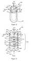
- Z-directed capacitor 600is comprised of center conductive channel 601 and a body 605 comprised of a top member 605 t , a bottom member 605 b , and a plurality of support members 610 (illustrated as disks) between the top and bottom members 605 t , 605 b.
- Center conductive channel 601extends through openings 615 in the assembled Z-directed capacitor 600 and openings 602 t and 602 b , all of which are sized to closely receive the center conductor.
- Center conductive channel 601is electrically connectable to conductive traces 603 t and 603 b on the top and bottom portions 605 t , 605 b forming a signal path for signal 626 . This connection is made by plating or soldering.
- Center conductive channel 601is connected to signal 626 via conductive trace 603 t .
- the bottom end of conductive channel 601is connected in a similar fashion to a signal trace (not shown) via conductive trace 603 b.
- Opposed openings 607 t and 608 tare provided at the edge of top portion 605 t .
- Bottom portion 605 bis of similar construction as top portion 605 t having opposed openings 607 b and 608 b provided at the edge.
- Between top and bottom portions 605 t , 605 bare a plurality of support members 610 , which provide the capacitive feature.
- Support members 610each have at least one opening 613 at their outer edge and an inner hole 615 allowing for passage of conductive channel 601 therethrough. As shown, two opposed openings 613 are provided in each support member 610 .
- the opposed openings 607 t , 607 b , 608 t , 608 b , and 613align to form opposed side channels 604 and 608 extending along the side surface of Z-directed capacitor 600 .
- Side channel 604is shown connected to reference voltage such as ground 620 and side channel 606 to another reference voltage such as V CC 622 .
- Support members 610may be fabricated from a dielectric material and may be all of the same or varying thickness allowing for choice in designing the desired properties for Z-directed capacitor 600 .
- Annular plating 617is provided on one of top and bottom surfaces of support member 610 or, if desired, on both surfaces. Annular plating is shown on the top surface of each support member but location of the annular plating can vary from support member to support member. Annular plating 617 generally conforms to the shape of the support member and extends from one of the edge openings 613 toward the other if an additional opening is provided.
- the annular plate 617is of a diameter or dimension or overall size that is less than the diameter, dimension or overall size of support member 610 on which it is affixed.
- the plate 617is described as annular, other shapes may also be used provided that the plating does not contact the center conductive channel or extend to the edge of the support member on which it is plated or otherwise affixed.
- the annular platedoes contact one of the edge openings 613 but is spaced apart from the other openings if more than one channel is present in the side surface of the body of Z-directed capacitor 600 .
- the support members 610are substantially identical except that when stacked, alternate members are rotated 180 degrees with respect to the member above or below it. This may be referred to as a 1-1 configuration. In this way, alternate members will be connected to one or the other of the two side channels. As shown in FIG. 13 , the annular plating on the upper one of the two support members 610 is connected to side channel 608 and voltage V CC 622 while the annular plating on the lower one of the two support members 610 is connected to side channel 604 and ground 620 . Other support member arrangements may also be used such as having two adjacent members connected to the same channel with the next support member being connected to the opposite channel which may be referred to as a 2-1 configuration.
- Other configurationsmay include 2-2, 3-1 and are a matter of design choice.
- the desired capacitance or voltage ratingdetermines the number of support members that are inserted between top and bottom portions 605 t , 605 b .
- dielectric memberscomprised of dielectric material and similarly shaped to support members 610 may be interleaved with support members 610 .
- only a single channelmay be used or more channels may be provided and/or the annular plating may be brought into contact with the center conductive channel and not in contact with the side channels.
- the embodiments for Z-directed capacitorsare for purposes of illustration and are not meant to be limiting.
- a second conductive channelmay be provided in parallel with the first conductive channel that is disposed within the conductive plates to create a differential decoupling capacitor.
- Another embodiment of a Z-directed capacitorcan be constructed from FIG. 12 or FIG. 13 by connecting the center conductive channel to one of the reference voltages at each support member that also has its annular plating connected to the same reference voltage. This may be accomplished simply by connecting the conductive channel to the annular plating as schematically illustrated by the jumper 621 .
- the annular opening 619 in the annular plate 617would be sized so that the annular plate and conductive channel 601 would be electrically connected. This component may be placed directly below a power pin or ball of an integrated circuit or other surface mounted component for optimum decoupling placement.
- Z-directed signal pass-through components illustrated in FIGS. 8-11 and the Z-directed decoupling capacitors illustrated in FIGS. 12 and 13provide merely a few example applications of a Z-directed component.
- Those skilled in the artwill appreciate that various other types of Z-directed components may be utilized including, but not limited to, transmission lines, delay lines, T filters, decoupling capacitors, inductors, common mode chokes, resistors, differential pair pass throughs, differential ferrite beads, diodes, or ESD protection devices (varistors).
- the bodies of the Z-directed componentsare formed from a material forming the component substrate.
- the substrate materialmay also be mixed with a binder material as is known in the art.
- a variety of different Z-directed componentsare contemplated herein including, but not limited to, transmission lines, delay lines, T filters, decoupling capacitors, inductors, common mode chokes, resistors, differential pair pass throughs, differential ferrite beads, diodes, and ESD protection devices (varistors). Accordingly, it will be appreciated that the substrate material used will depend on the Z-directed component desired.
- the substrate materialmay include a single dielectric material that has a relative permittivity from about 3, e.g., polymers, to over 10,000, e.g., barium titanate (BaTiO 3 ).
- a material with a relatively high dielectric valuemay be used in a Z-directed decoupling capacitor and a material with a relatively low dielectric value may be used in a Z-directed signal pass-through component. If a Z-directed component is desired to have an inductive function or a delay line then a ferrite material may be selected that has a low or high relative permeability with a range of about 1 to about 50,000.
- a conductive materialmay be mixed with a dielectric material to create a desired resistance.
- these or other compatible materialsmay be mixed together to form a component layer.
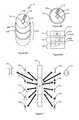
- Extrusion die 700defining the shape of the Z-directed component layer(s) according to one embodiment is illustrated.
- Extrusion die 700includes a chamber 703 having an inlet 701 and an outlet 702 for passing the component substrate material therethrough.
- a generally cylindrical chamber 703is used; however, as discussed above, many different shapes may be used.
- an interior projection 704is provided that forms a corresponding interior channel in the component layer(s).
- a pair of projections 705 , 706 along an edge 703 e of chamber 703are also included that form a corresponding pair of side channels in the component layer(s).
- projection 704is cylindrical and projections 705 , 706 are semi-cylindrical; however, any suitable shape may be used as desired depending on the desired shape of the channels in the component layer(s). Further, although one interior projection 704 and two side projections 705 , 706 are illustrated; any suitable number of side and/or interior projections may be used depending on the desired number of side and interior channels, respectively, through the component layer(s).
- extrusion die 700includes one or more interior projections for forming an interior channel in the component layer(s), such as interior projection 704
- a support member 707is needed to physically support the interior projection from one or more points along edge 703 e of chamber 703 .
- support member 707connects interior projection 704 with both side projections 705 , 706 to support interior projection 704 .
- One or more layers of the Z-directed componentare formed by forcing a blank 708 containing the substrate material through extrusion die 700 using a ram (not shown).
- blank 708is composed of green (unfired) ceramic; however, various substrate materials may be used as discussed above.
- blank 708is pressed into inlet 701 through chamber 703 which causes the substrate material to take on the shape of chamber 703 .
- projections 704 , 705 , 706form the desired channels through the substrate material.
- a direct extrusion processmay be used where extrusion die 700 is held stationary and the ram is moved towards it or an indirect extrusion process may be used where the ram is held stationary and extrusion die 700 is moved towards it.
- a combination of the twomay be also used where the ram and die 700 are moved towards each other.
- a hydrostatic extrusion processmay be used where fluid pressure is used to force blank 708 through die 700 .
- Extrusion die 700may be oriented horizontally, vertically or at any suitable angle thereto. Any conventional drive may be applied to provide the extruding force including a mechanical or hydraulic drive.
- the corresponding support member 707will create an undesired gap in the extruded substrate material.
- Support member 707is preferably thin in order to minimize the size of this gap.
- the substrate materialis divided in half by support member 707 .
- FIG. 15Awhich shows a cutaway view of chamber 703
- one way to remove this gap, shown as gap 710is to recombine the halves 708 a , 708 b of the substrate material in the output 702 of chamber 703 (or a separate chamber attached thereto).
- the diameter of chamber 703may decrease slightly in the downstream direction D of extrusion past projections 704 , 705 , 706 in order to urge halves 708 a , 708 b toward each other. As shown in FIG. 15A , this causes gap 710 to reduce as the substrate material advances until halves 708 a , 708 b combine to eliminate gap 710 .
- the downstream edge of support member 707may taper like a blade such that its thickness decreases in downstream direction D in order to promote recombination of halves 708 a , 708 b .
- the upstream edge of support member 707may also taper to provide a cleaner cut into blank 708 in order to facilitate recombination.
- a movable element 712such as a plug or rod, supports the downstream end of the substrate material as it advances to help prevent the channels from narrowing as gap 710 is eliminated.
- plug 712supports the substrate material from below and lowers according to the speed of extrusion in order to maintain the shape of the substrate material.
- Projections 704 , 705 , 706can also be extended in downstream direction D as desired to prevent the channels from losing their shape.
- the substrate material exiting extrusion die 700includes the desired channels therein but not the undesired gap 710 caused by support member 707 .
- an alternative for forming interior channels in the component layer(s) without forming an undesired gapis to extrude the material in separate segments, such as halves, and then to combine the segments after extrusion.
- an extrusion die having an interior support membersuch as support member 707 of extrusion die 700 shown in FIGS. 14A and 14B
- the halvesmay be removed from the extrusion die and then combined.
- a common extrusion diemay be used to extrude each segment separately.
- extrusion die 720having an inlet 721 , and outlet 722 and a chamber 723 is used to form the component layer(s) in halves.
- Extrusion die 720includes a projection 724 for forming an interior channel and a projection 726 for forming a side channel in the component layer(s).
- Projections 724 , 726are each positioned along an edge 723 e of chamber 723 thereby eliminating the need for an interior support member, such as support member 707 shown in FIG. 14B .
- projection 726is sized and shaped to form a complete side channel through each extruded segment.
- projection 724is sized and shaped to form only a partial interior channel through each extruded segment such that when the extruded segments are combined, the corresponding partial interior channels created by projection 724 are combined to form a complete interior channel through the component layer(s).
- the void created by projection 724 in a first extruded segmentis matched with a corresponding void created by projection 724 in a second extruded segment to create a complete interior channel in the component layer(s).
- the void created by projection 726 in the first extruded segmentcreates a first side channel in the component layer(s) and the void created by projection 726 in the second extruded segment creates a second side channel in the component layer(s).
- the corresponding extruded segmentscan be combined by matably aligning the segments and then applying a substantially uniform radial pressure. In the unfired state, the extruded segments will tend to adhere to one another upon being pressed together by the applied radial pressure.
- An adhesivecould also be used to join the segments to each other. The adhesive can be baked off when the substrate material is fired or it can be a high temperature adhesive that survives the firing process provided that the impurity in the substrate material caused by the adhesive will not inhibit performance of the Z-directed component.
- Another alternative for forming interior channels in the component layer(s) without forming an undesired gapis to simply extrude the layer(s) using an extrusion die that does not include any interior projections that require support and then form the desired interior channel(s) after the extrusion process is completed.
- the desired interior channel(s)may be formed by conventional methods known in the art such as drilling or laser cutting through the extruded substrate material.
- the substrate materialcan be partially fired in order to improve the strength of the material and to ensure that it will remain intact before proceeding with the remaining steps.
- the substrate materialmay be cut into two or more individual component layers depending on the particular Z-directed component being made. For example, if the Z-directed component is intended to possess significant capacitance between any of the conductive paths the substrate material will be layered. Alternatively, if the Z-directed component only requires interior and/or side channels for signal and ground return paths, then the entire Z-directed component may be extruded at once. Conductive material can then be applied to the interior and/or side channels and across the top and/or bottom surface of the component to provide one or more traces for connection with the PCB as discussed below.
- FIG. 17shows a segment of extruded substrate material 730 ready to be cut.
- One optionis to use a series of blades 732 spaced according to a predetermined distribution to create the component layers.
- the component layersrange in thickness from 0.5 mil to about 62 mil (about 0.0127 mm to about 1.57 mm), including all increments and values therebetween, depending on the application in which the Z-directed component will be used.
- Another optionis to cut the extruded substrate material 730 using multiple passes of a single blade.
- the thickness of each component layeris determined by controlling the timing of each pass of the blade.
- Each component layermay have substantially the same thickness or different thicknesses may be used.
- a feedback mechanismmay be used to adjust the timing of the cuts in order to account for parameters that may change with blade usage, such as the kerf of the blade.
- FIG. 18shows a post-cut layer 740 of the Z-directed component formed by extrusion die 700 .
- Layer 740includes one center channel 742 a and two side channels 742 b , 742 c that correspond with projections 704 , 705 and 706 , respectively.
- the shape of layer 740 and the number of channels 742 therein, as well as their placement and shape,can be altered by the changing the shape of the extrusion die chamber used including the number and placement of projections therein.
- layer 740is ready to receive conductive material on at least one surface thereof.
- Conductive materialmay be applied to one or more of channels 742 a , 742 b , 742 c , a top surface 740 t and/or both top surface 740 t and a bottom surface of layer 740 .
- Layer 740is transferred to a tool having restraining and locating ability, such as a conveyor belt, to receive conductive material.
- layer 740may be placed in a cavity 744 in a constraining plate 746 that has a side wall surface 748 that is spaced from the side channels 742 b , 742 c in the component layer 740 such that a gap 749 is formed therebetween ( FIG. 19 ).
- This spacingallows conductive material to flow into gap 749 to plate the desired side channel(s) 742 b , 742 c .
- Another alternative to plate side channels 742 b , 742 cis to apply conductive material after the Z-directed component has been assembled by painting, jetting, sputter, or other known methods.
- FIG. 20shows an example mask in the form of a physical mask 750 that is placed on top surface 740 t of layer 740 .
- the diagonal hatching included in FIG. 20illustrates the openings in mask 750 .
- Mask 750includes a center opening 752 that permits conductive material to flow into and plate center conductive channel 742 a .
- Mask 750also includes a pair of peripheral openings 754 a , 754 b that permit conductive material to plate top surface 740 t .
- Peripheral openings 754 a , 754 bare separated by a thin mask portion 756 that also separates center opening 752 from peripheral openings 754 a , 754 b .
- Portion 756is required when one or more conductive channels through the interior of the layer 740 are desired in order to provide one or more interior openings in the mask such as center opening 752 in mask 750 .
- Mask 750includes a pair of scalloped portions 758 a , 758 b that are positioned above side channels 742 b , 742 c in the example embodiment illustrated.
- Scalloped portion 758 bprojects slightly further inward than scalloped portion 758 a .
- conductive materialis permitted to flow onto the portion of top surface 740 t that connects with side channel 742 b but conductive material is not permitted to connect with side channel 742 c.
- the resulting plated layer 740 utilizing example mask 750is shown in FIG. 21 having conductive material 760 thereon. As shown, center channel 742 a has been plated with conductive material 760 . Top surface 740 t of layer 740 has been plated to make a connection with side channel 742 b but not side channel 742 c .
- the mask 750 shown in FIG. 20is intended to illustrate one example of a suitable mask. Alternative masks may be employed depending on such factors as the shape of the layer, the number of center channels and/or side channels that require plating, and the plating pattern desired for top surface 740 t.
- a photoresist maskmay be applied using photochemical methods known in the art.
- a radiation-sensitive photoresistis applied to top surface 740 t and then selectively exposed to a radiation source, such as X-ray or UV light.
- the photoresistis then developed to wash away the areas where the photoresist layer is not desired.
- positive or negative photoresistsmay be used as desired.
- Conductive materialcan then be screened through the photoresist mask onto top surface 740 t of the component layer 740 such as by spin coating liquid conductive material on top of the photoresist mask. After the conductive material is applied, the remaining photoresist can then be removed.
- a selective jetting processis used to apply conductive material to top surface 740 t and/or channel(s) 742 .
- liquid conductive materialis applied to the component layer 740 using a fluid ejection mechanism as is known in the art.
- etchable conductive materialanother alternative is to spin coat or otherwise apply a layer of liquid conductive material across the entire top surface 740 t and then selectively etch the conductive material from top surface 740 t to form the desired conductive pattern thereon.
- Another alternativeis to first selectively apply a seed layer of conductive material to the component layer 740 and then apply additional conductive material by electrolysis techniques.
- One suitable method for applying the seed layerincludes the use of photochemical methods. A photoresist layer is applied across the entire top surface 740 t of the Z-directed component layer 740 and then selectively exposed to a radiation source. The photoresist is then developed to wash away the areas where the photoresist layer is not desired. Again, positive or negative photoresists may be used as desired. Conductive material is then applied across the entire top surface 740 t of the Z-directed component layer 740 . The remainder of the photoresist is then etched away thereby also removing the conductive material from those areas where the seed layer is not desired. Electrolysis techniques are then applied to thicken the layer of conductive material on the component layer 740 .
- channel(s) 742do not need to be plated after each layer is formed. Rather, channel(s) 742 may be filled with conductive material after the component layers are stacked together.
- the Z-directed componentis formed from a stack of component layers 740 .
- Each layermay be formed from the same substrate material or some layers may be formed from different substrate materials.
- a conveyormay be used to move all of the component layers 740 for stacking after they are formed.
- the outside features of the layers 740may be used to align the layers 740 with each other.
- each layer 740is alternatively stacked by rotating it 180 degrees with respect to the layer 740 immediately below creating positive and negative terminals on two sides of the Z-directed component. The stacking is performed in a constraining plate that keeps the stack in position.
- a Z-directed component 764may be desired that includes partial side channels 742 that are twisted or offset from each other between the top and bottom halves of the component 764 as shown in FIG. 23 .
- This type of componentmay be desired in order to permit an interior signal to enter on one side of the Z-directed component 764 and exit at a 90 degree angle thereto without running into a side channel 742 .
- This offsetcan be accomplished by rotating the layers 740 as they are stacked.
- FIG. 24shows a cutaway view of the stack of layers 740 positioned in a cavity 772 of a constraining plate 770 .
- a movable componente.g., a rod or a plug, applies a desired force to one end of the stacked layers to create the desired pressure profile for the materials chosen.
- opposing plugs 774 , 776apply pressure from opposite ends of the stacked layers 740 .
- Heating elementscan be embedded into the walls of cavity 772 in order to supply a desired temperature profile to the stacked layers 740 .
- a full firing processis performed in plate 770 . However, this may be difficult due to the extreme temperatures that are subjected to the constraining elements.
- a chamfer, dome or other form of taper or lead-in of at least one of the top and bottom edge of the Z-directed componentis desired in order to ease insertion of the Z-directed component into the mounting hole in the PCB.
- FIG. 25Ashows a Z-directed component 780 having a dome 782 formed on an end thereof.
- FIG. 25Bshows a Z-directed component 784 having a chamfered end 786 .
- the dome 782 or chamfer 786may be part of the component or attached thereto. In one embodiment, the dome 782 or chamfer 786 is a separate part that is partially inserted into the mounting hole in the PCB.
- the Z-directed componentis then inserted behind the dome 782 or chamfer 786 to push it through the mounting hole causing the dome 782 or chamfer 786 to expand the mounting hole and prevent the component from cutting or tearing the PCB.
- the dome 782 or chamfer 786may be configured to remain attached to the Z-directed component following insertion into the mounting hole in the PCB or it may be used to facilitate insertion and then removed.
- One method for forming the desired taper as part of the Z-directed componentutilizes a plug 790 having a recess 792 formed in an end 794 thereof having a tapered rim 796 around a periphery of recess 792 as shown in FIG. 26 .
- Tapered rim 796is chamfered in the example embodiment illustrated; however, a domed, elliptical or rounded rim may also be used depending on the shape of the taper desired.
- Plug 790is used to compress the stacked component layers as discussed above.
- the end of the partis reflowed to have the desired geometry and the conductive path(s) on the end of the part are allowed to continue across or through the corresponding taper formed on the end of the part.
- the tapered end portion of the partcan then be used to facilitate board to board electrical connections in multi-PCB applications. It will be appreciated that where the desired taper extends across multiple component layers, successive layers of the Z-directed component forming the taper will have decreasing diameters (or widths in the case of a component layer with a non-circular cross-section). Alternatively, the desired taper may be formed in a single component layer.
- a firing processis applied to solidify the part if it has not been done so already.
- the firing processalso shrinks the part to its final dimensions.
- the Z-directed componentcan be tested for yield and performance and any additional processes may be performed as desired.
- the pressing and heating stepsmay cause burrs to form.
- the Z-directed componentsare tumbled with various abrasive agents to smooth the corners and edges of the part.
- resist areasmay be added to the Z-directed component to keep the conductive materials from sticking to areas that are not intended to be conductive.
- Glue areasmay be applied to the component to assist with retaining it in the PCB. Visible markings and/or locating features may be added to the Z-directed component to assist with assembly into the PCB.
- the Z-directed componentis ready to be inserted into the mounting hole of the PCB.
- the componentmay be mounted normal to the plane of the PCB from the top or bottom surfaces or both surfaces, mounted at an angle thereto or inserted into the edge of the PCB between the top and bottom surfaces of the PCB.
- the Z-directed componentis press fit into the mounting hole. This press fit may be in the form of an interference fit between the component and the mounting hole.
- a conductive plating bridgemay be applied to connect one or more traces on the top and/or bottom surface of the component to a corresponding trace on the PCB.
- additional conductive platingmay be applied to these side channels to form the desired signal connections between the Z-directed component and the PCB.
- an adhesive 806is applied to a surface 808 of PCB 804 external to mounting hole 802 .
- Adhesive 806is positioned to contact a surface of Z-directed component 800 when it is inserted into mounting hole 802 in order to fix the location of Z-directed component 800 and prevent it from rotating or translating out of position.
- a conductive strip 812is formed along a side surface 810 s of a Z-directed component 810 .
- Conductive strip 812runs along side surface 810 s to either the top or bottom surface of Z-directed component 810 .
- conductive strip 812may be applied after the Z-directed component 810 is formed.
- conductive strip 812may be formed during fabrication of Z-directed component 810 such as by applying conductive material to a predetermined portion of the component layer(s) 740 as discussed above.
- conductive strip 812runs along side surface 810 s to a top surface 810 t of Z-directed component 810 .
- conductive strip 812forms a bridge between a trace 814 on the respective top or bottom surface of Z-directed component 810 and a trace 816 on a PCB 818 when the top or bottom surface of the Z-directed component extends past the corresponding top or bottom surface of the PCB.
- trace 814 on Z-directed component 810is able to connect to trace 816 on PCB 818 even if the top or bottom surface of Z-directed component 810 is not flush with the corresponding top or bottom surface of PCB 818 .
- conductive strip 812runs from top surface 810 t of Z-directed component 810 to a point along side surface 810 s that is below the top surface of the PCB 818 . In one embodiment, conductive strip 812 extends into the side of Z-directed component 810 both to decrease its resistance and to ensure that it is not removed if another feature such as a taper is later applied to Z-directed component 810 .
Landscapes
- Engineering & Computer Science (AREA)
- Microelectronics & Electronic Packaging (AREA)
- Manufacturing & Machinery (AREA)
- Structures For Mounting Electric Components On Printed Circuit Boards (AREA)
- Structure Of Printed Boards (AREA)
- Production Of Multi-Layered Print Wiring Board (AREA)
Abstract
Description
Claims (7)
Priority Applications (13)
| Application Number | Priority Date | Filing Date | Title |
|---|---|---|---|
| US13/250,812US8752280B2 (en) | 2011-09-30 | 2011-09-30 | Extrusion process for manufacturing a Z-directed component for a printed circuit board |
| US13/284,084US8943684B2 (en) | 2011-08-31 | 2011-10-28 | Continuous extrusion process for manufacturing a Z-directed component for a printed circuit board |
| US13/528,097US9009954B2 (en) | 2011-08-31 | 2012-06-20 | Process for manufacturing a Z-directed component for a printed circuit board using a sacrificial constraining material |
| CN201280047691.XACN103858066B (en) | 2011-09-30 | 2012-09-24 | Extrusion process for the Z manufactured for printed circuit board (PCB) the parts being orientated |
| HK15100286.6AHK1199960B (en) | 2011-09-30 | 2012-09-24 | Extrusion process for manufacturing a z-directed component for a printed circuit board |
| PCT/US2012/056840WO2013048937A1 (en) | 2011-09-30 | 2012-09-24 | Extrusion process for manufacturing a z-directed component for a printed circuit board |
| SG11201400182UASG11201400182UA (en) | 2011-09-30 | 2012-09-24 | Extrusion process for manufacturing a z-directed component for a printed circuit board |
| KR1020147010299AKR101947355B1 (en) | 2011-09-30 | 2012-09-24 | Extrusion process for manufacturing a z-directed component for a printed circuit board |
| EP12836913.9AEP2761392B1 (en) | 2011-09-30 | 2012-09-24 | Extrusion process for manufacturing a z-directed component for a printed circuit board |
| US14/268,265US20140237816A1 (en) | 2011-09-30 | 2014-05-02 | Extrusion Process for Manufacturing a Z-Directed Component for a Printed Circuit Board |
| US14/574,903US9564272B2 (en) | 2011-08-31 | 2014-12-18 | Continuous extrusion method for manufacturing a Z-directed component for insertion into a mounting hole in a printed circuit board |
| US14/631,192US9814145B2 (en) | 2011-08-31 | 2015-02-25 | Methods for manufacturing a Z-directed printed circuit board component having a removable end portion |
| US15/397,829US10160151B2 (en) | 2011-08-31 | 2017-01-04 | Continuous extrusion method for manufacturing a Z-directed component for insertion into a mounting hole in a printed circuit board |
Applications Claiming Priority (1)
| Application Number | Priority Date | Filing Date | Title |
|---|---|---|---|
| US13/250,812US8752280B2 (en) | 2011-09-30 | 2011-09-30 | Extrusion process for manufacturing a Z-directed component for a printed circuit board |
Related Child Applications (1)
| Application Number | Title | Priority Date | Filing Date |
|---|---|---|---|
| US14/268,265DivisionUS20140237816A1 (en) | 2011-09-30 | 2014-05-02 | Extrusion Process for Manufacturing a Z-Directed Component for a Printed Circuit Board |
Publications (2)
| Publication Number | Publication Date |
|---|---|
| US20130081267A1 US20130081267A1 (en) | 2013-04-04 |
| US8752280B2true US8752280B2 (en) | 2014-06-17 |
Family
ID=47991280
Family Applications (2)
| Application Number | Title | Priority Date | Filing Date |
|---|---|---|---|
| US13/250,812Active2032-05-04US8752280B2 (en) | 2011-08-31 | 2011-09-30 | Extrusion process for manufacturing a Z-directed component for a printed circuit board |
| US14/268,265AbandonedUS20140237816A1 (en) | 2011-09-30 | 2014-05-02 | Extrusion Process for Manufacturing a Z-Directed Component for a Printed Circuit Board |
Family Applications After (1)
| Application Number | Title | Priority Date | Filing Date |
|---|---|---|---|
| US14/268,265AbandonedUS20140237816A1 (en) | 2011-09-30 | 2014-05-02 | Extrusion Process for Manufacturing a Z-Directed Component for a Printed Circuit Board |
Country Status (6)
| Country | Link |
|---|---|
| US (2) | US8752280B2 (en) |
| EP (1) | EP2761392B1 (en) |
| KR (1) | KR101947355B1 (en) |
| CN (1) | CN103858066B (en) |
| SG (1) | SG11201400182UA (en) |
| WO (1) | WO2013048937A1 (en) |
Cited By (1)
| Publication number | Priority date | Publication date | Assignee | Title |
|---|---|---|---|---|
| US20170113392A1 (en)* | 2011-08-31 | 2017-04-27 | Lexmark International, Inc. | Continuous extrusion method for manufacturing a z-directed component for insertion into a mounting hole in a printed circuit board |
Families Citing this family (4)
| Publication number | Priority date | Publication date | Assignee | Title |
|---|---|---|---|---|
| US20130341078A1 (en)* | 2012-06-20 | 2013-12-26 | Keith Bryan Hardin | Z-directed printed circuit board components having a removable end portion and methods therefor |
| CN102917535A (en)* | 2012-11-16 | 2013-02-06 | 东莞生益电子有限公司 | Thermally conductive metal core and PCB board using the thermally conductive metal core |
| US11948724B2 (en)* | 2021-06-18 | 2024-04-02 | Vishay Dale Electronics, Llc | Method for making a multi-thickness electro-magnetic device |
| CN115135012B (en)* | 2022-06-28 | 2025-08-19 | 生益电子股份有限公司 | Plug groove structure, step groove manufacturing method and step plate |
Citations (147)
| Publication number | Priority date | Publication date | Assignee | Title |
|---|---|---|---|---|
| US2005582A (en) | 1934-03-06 | 1935-06-18 | Bell Telephone Labor Inc | Inductive device |
| US2188667A (en) | 1935-01-08 | 1940-01-30 | Globe Union Inc | Resistor and method of making the same |
| US3142783A (en)* | 1959-12-22 | 1964-07-28 | Hughes Aircraft Co | Electrical circuit system |
| US3148356A (en) | 1959-09-14 | 1964-09-08 | Jr George A Hedden | Printed circuit connector |
| US3219886A (en) | 1959-12-28 | 1965-11-23 | Bunker Ramo | Modular circuit fabrication |
| US3262033A (en) | 1963-09-05 | 1966-07-19 | John H Culbertson | Variable capacitor |
| US3377611A (en) | 1966-12-12 | 1968-04-09 | Walter S. Pawl | Rigid parallel sided squeeze slot connector |
| US3545079A (en) | 1968-05-02 | 1970-12-08 | Vitramon Inc | Method of making multilayer circuit system |
| US3652971A (en) | 1970-02-11 | 1972-03-28 | Kendick Mfg Co | Self-aligning slip ring capsule |
| US3666160A (en) | 1970-06-30 | 1972-05-30 | Contacts Inc | Method and apparatus for feeding discrete parts to a cold heading machine |
| US3691326A (en) | 1971-06-14 | 1972-09-12 | Abraham Grossman | Rotary thumbwheel switch construction |
| US3798394A (en) | 1972-10-11 | 1974-03-19 | Bell Telephone Labor Inc | Keyboard switch assembly with conductive diaphragm operators and rotary switch operators for adjustably selecting a multidigit number |
| US3996440A (en) | 1975-04-04 | 1976-12-07 | Rca Corporation | Multiposition rotary switch with detent means |
| US4109295A (en) | 1977-08-01 | 1978-08-22 | Ncr Corporation | Solderless circuit board component |
| US4109296A (en) | 1977-08-01 | 1978-08-22 | Ncr Corporation | Machine insertable circuit board electronic component |
| GB1524388A (en) | 1974-10-10 | 1978-09-13 | Philips Electronic Associated | Extruding hollow glass bodies |
| US4147579A (en) | 1975-07-17 | 1979-04-03 | Siemens Aktiengesellschaft | Method of producing an electric component consisting of elements joined by an insulating co-polymer layer |
| US4199209A (en) | 1978-08-18 | 1980-04-22 | Amp Incorporated | Electrical interconnecting device |
| WO1980001146A1 (en) | 1978-12-04 | 1980-06-12 | Caterpillar Tractor Co | Method of making and using a ceramic shell mold |
| US4381134A (en) | 1981-03-13 | 1983-04-26 | Bell Telephone Laboratories, Incorporated | Electrical connector for plated-through holes |
| WO1983001923A1 (en) | 1981-11-27 | 1983-06-09 | Mortensen, Louis, Aackersberg | A method and a former member for tapering an end portion of an extruded tubular plastic member said former being used as a sales unit |
| US4446505A (en) | 1982-03-22 | 1984-05-01 | Amp Incorporated | Electrical connector for interconnecting printed circuit boards |
| US4543715A (en) | 1983-02-28 | 1985-10-01 | Allied Corporation | Method of forming vertical traces on printed circuit board |
| US4561486A (en) | 1981-04-30 | 1985-12-31 | Hoxan Corporation | Method for fabricating polycrystalline silicon wafer |
| US4642588A (en) | 1983-05-26 | 1987-02-10 | Elmec Corporation | Method for adjustment of variable delay line |
| US4654472A (en) | 1984-12-17 | 1987-03-31 | Samuel Goldfarb | Electronic component package with multiconductive base forms for multichannel mounting |
| US4654749A (en) | 1985-07-30 | 1987-03-31 | Murata Manufacturing Co., Ltd. | High-voltage ceramic capacitor and method of producing the same |
| US4675625A (en) | 1985-03-26 | 1987-06-23 | Rogers Corporation | Rolled delay line of the coplanar line type |
| US4700155A (en) | 1982-09-10 | 1987-10-13 | Murata Manufacturing Co., Ltd. | Feedthrough noise eliminating filter having integrally stepped mounting portion |
| US4711015A (en) | 1984-10-17 | 1987-12-08 | Metalmeccanica Gori & Zucchi M.G.Z, S.P.A. | Apparatus for handling and assembling axial electronic components on printed circuit cards |
| US4735753A (en) | 1986-07-28 | 1988-04-05 | Ackermann Walter T | Method of making a fastener |
| US4775326A (en) | 1985-12-06 | 1988-10-04 | Burndy Electra N.V. | Contact pin |
| US4789346A (en) | 1987-03-27 | 1988-12-06 | Amp Incorporated | Solder post alignment and retention system |
| US4850892A (en) | 1985-12-16 | 1989-07-25 | Wang Laboratories, Inc. | Connecting apparatus for electrically connecting memory modules to a printed circuit board |
| US4913863A (en) | 1989-01-30 | 1990-04-03 | Hoechst Celanese Corporation | Split extrusion die assembly for thermoplastic materials and methods of using the same |
| US5010945A (en) | 1988-11-10 | 1991-04-30 | Lanxide Technology Company, Lp | Investment casting technique for the formation of metal matrix composite bodies and products produced thereby |
| US5147985A (en) | 1990-08-14 | 1992-09-15 | The Scabbard Corporation | Sheet batteries as substrate for electronic circuit |
| US5166096A (en) | 1991-10-29 | 1992-11-24 | International Business Machines Corporation | Process for fabricating self-aligned contact studs for semiconductor structures |
| US5344343A (en) | 1990-04-13 | 1994-09-06 | North American Specialties Corporation | Solder-bearing lead |
| US5406444A (en) | 1993-03-29 | 1995-04-11 | Medtronic, Inc. | Coated tantalum feedthrough pin |
| US5603847A (en) | 1993-04-07 | 1997-02-18 | Zycon Corporation | Annular circuit components coupled with printed circuit board through-hole |
| US5650759A (en) | 1995-11-09 | 1997-07-22 | Hittman Materials & Medical Components, Inc. | Filtered feedthrough assembly having a mounted chip capacitor for medical implantable devices and method of manufacture therefor |
| US5669789A (en) | 1995-03-14 | 1997-09-23 | Lucent Technologies Inc. | Electromagnetic interference suppressing connector array |
| US5760336A (en) | 1997-03-26 | 1998-06-02 | Wang; Jack | Burn and explosion-resistant circuit package for a varistor chip |
| US5783026A (en) | 1995-05-24 | 1998-07-21 | International Business Machines Corporation | Apparatus for stacking sheets by carriers |
| US5851865A (en) | 1995-09-05 | 1998-12-22 | Kabushiki Kaisha Toshiba | Method of manufacturing semiconductor device having mask layer forming step for ion implantation |
| US5858145A (en) | 1996-10-15 | 1999-01-12 | Sarnoff Corporation | Method to control cavity dimensions of fired multilayer circuit boards on a support |
| US5870921A (en) | 1997-07-31 | 1999-02-16 | Piccinin; Gabriel | Extrusion die for semi-hollow and hollow extruded shapes and tube |
| US5952723A (en) | 1992-12-25 | 1999-09-14 | Kawasaki Steel Corporation | Semiconductor device having a multilevel interconnection structure |
| US6045615A (en) | 1998-01-28 | 2000-04-04 | International Business Machines Corporation | Homogeneous screening nozzle |
| US6054649A (en) | 1997-08-08 | 2000-04-25 | Murata Manufacturing Co., Ltd. | Insulated wire with noise-suppressing function |
| US6068782A (en) | 1998-02-11 | 2000-05-30 | Ormet Corporation | Individual embedded capacitors for laminated printed circuit boards |
| US6153290A (en) | 1998-01-06 | 2000-11-28 | Murata Manufacturing Co., Ltd. | Multi-layer ceramic substrate and method for producing the same |
| US6165864A (en) | 1998-07-28 | 2000-12-26 | Siemens Aktiengesellschaft | Tapered electrode for stacked capacitors |
| US20010012036A1 (en) | 1999-08-30 | 2001-08-09 | Matthew Giere | Segmented resistor inkjet drop generator with current crowding reduction |
| US6319018B1 (en) | 2000-02-29 | 2001-11-20 | Avaya Technology Corp. | Circuit board electrical and physical connection system and method |
| US6329715B1 (en) | 1996-09-20 | 2001-12-11 | Tdk Corporation | Passive electronic parts, IC parts, and wafer |
| US6388208B1 (en) | 1999-06-11 | 2002-05-14 | Teradyne, Inc. | Multi-connection via with electrically isolated segments |
| US20020086188A1 (en) | 2000-10-12 | 2002-07-04 | Eugene Halsey | Reduced contrast improved transmission conductively coated transparent substrate |
| US20020117330A1 (en) | 1993-11-16 | 2002-08-29 | Formfactor, Inc. | Resilient contact structures formed and then attached to a substrate |
| JP2002316084A (en) | 2001-04-19 | 2002-10-29 | Tdk Corp | Spin coating apparatus using mask and mask for spin coating |
| US20030081370A1 (en) | 2001-10-15 | 2003-05-01 | Haskell Donald K. | Apparatus and process for the control of electromagnetic fields on the surface of EMI filter capacitors |
| US20030101585A1 (en) | 2001-06-22 | 2003-06-05 | Intel Corporation | Methods of manufacturing via intersect pad for electronic components |
| US6581276B2 (en) | 2000-04-04 | 2003-06-24 | Amerasia International Technology, Inc. | Fine-pitch flexible connector, and method for making same |
| US6593535B2 (en) | 2001-06-26 | 2003-07-15 | Teradyne, Inc. | Direct inner layer interconnect for a high speed printed circuit board |
| US6735855B2 (en) | 1999-03-10 | 2004-05-18 | Micron Technology, Inc. | Methods for electrical connector |
| US6747217B1 (en) | 2001-11-20 | 2004-06-08 | Unisys Corporation | Alternative to through-hole-plating in a printed circuit board |
| US6754551B1 (en) | 2000-06-29 | 2004-06-22 | Printar Ltd. | Jet print apparatus and method for printed circuit board manufacturing |
| US20040121266A1 (en) | 2002-12-23 | 2004-06-24 | Samsung Electro-Mechanics Co., Ltd. | Printed circuit board with embedded capacitors therein, and process for manufacturing the same |
| US20040224558A1 (en) | 2003-05-09 | 2004-11-11 | Qing Wan | Stacked electrical connector assembly with enhanced grounding arrangement |
| US20040242082A1 (en) | 2003-05-30 | 2004-12-02 | Sumitomo Wiring Systems, Ltd. | Terminal |
| US6870252B2 (en) | 2003-06-18 | 2005-03-22 | Sun Microsystems, Inc. | Chip packaging and connection for reduced EMI |
| US20050128680A1 (en) | 2003-12-15 | 2005-06-16 | Samsung Electro-Mechanics Co., Ltd. | Method of manufacturing multilayered ceramic capacitor by spin coating and multilayered ceramic capacitor |
| US20050156319A1 (en) | 2002-05-23 | 2005-07-21 | Stefano Oggioni | Structure of stacked vias in multiple layer electronic device carriers |
| US6920673B2 (en) | 2002-01-02 | 2005-07-26 | Greatbatch-Hittman, Inc. | Installation of filter capacitors into feedthroughs for implantable medical devices |
| US6950066B2 (en) | 2002-08-22 | 2005-09-27 | Skycross, Inc. | Apparatus and method for forming a monolithic surface-mountable antenna |
| US6948943B2 (en) | 2002-03-06 | 2005-09-27 | Intel Corporation | Shunting arrangements to reduce high currents in grid array connectors |
| US20050286238A1 (en) | 2004-06-24 | 2005-12-29 | Joy Stephen C | Device and method of manufacture of an interconnection structure for printed circuit boards |
| US6983535B2 (en) | 2001-02-01 | 2006-01-10 | International Business Machines Corporation | Insertion of electrical component within a via of a printed circuit board |
| US20060009038A1 (en) | 2004-07-12 | 2006-01-12 | International Business Machines Corporation | Processing for overcoming extreme topography |
| US20060054352A1 (en) | 2004-09-15 | 2006-03-16 | Samsung Electro-Mechanics Co., Ltd. | Printed circuit board including embedded passive component and method of fabricating same |
| US20060137907A1 (en) | 2004-12-29 | 2006-06-29 | Hewlett-Packard Development Company, L.P. | Component for impedance matching |
| US20060145800A1 (en) | 2004-08-31 | 2006-07-06 | Majid Dadafshar | Precision inductive devices and methods |
| US7101730B2 (en) | 2000-06-02 | 2006-09-05 | Micron Technology, Inc. | Method of manufacturing a stackable ball grid array |
| US20060215380A1 (en) | 2005-03-24 | 2006-09-28 | Agency For Science, Technology And Research | Embedded capacitor structure |
| US20060243581A1 (en) | 2005-04-27 | 2006-11-02 | Takumi Nishimoto | Rotary electronic component |
| WO2006121818A2 (en) | 2005-05-05 | 2006-11-16 | Rodrigo Alvarez Icaza Rivera | Dielectric elastomer fiber transducers |
| US20060266549A1 (en) | 2005-05-28 | 2006-11-30 | Hon Hai Precision Industry Co., Ltd. | Printed circuit board with differential vias arrangement |
| US20060278072A1 (en) | 2005-03-15 | 2006-12-14 | Kent Harold B | System and method for attaching a substantially three dimensional structure to a substantially two dimensional structure |
| US20060286696A1 (en) | 2005-06-21 | 2006-12-21 | Peiffer Joel S | Passive electrical article |
| US20070051594A1 (en) | 2003-04-30 | 2007-03-08 | Sebastian Schwarz | Electric rotary switch |
| US20070085125A1 (en) | 2004-07-28 | 2007-04-19 | Kabushiki Kaisha Toshiba | Semiconductor device including a conductive layer buried in an opening and method of manufacturing the same |
| US20070099513A1 (en) | 2005-10-31 | 2007-05-03 | Savage Dan J | Plug-in device and method of making the same |
| US20070124930A1 (en) | 2005-12-02 | 2007-06-07 | Cisco Technology, Inc. | Coaxial via in PCB for high-speed signaling designs |
| US20070138646A1 (en) | 2004-08-13 | 2007-06-21 | Raytheon Company | Integrated Circuit Resistor |
| US7238892B2 (en) | 2005-07-25 | 2007-07-03 | Hewlett-Packard Development Company, L.P. | Printed circuit board including pads with vacancies |
| US20070257761A1 (en) | 2006-05-08 | 2007-11-08 | Ibiden Co., Ltd. | Inductor and electric power supply using it |
| US20080013250A1 (en) | 2006-07-12 | 2008-01-17 | Tdk Corporation | Multilayer capacitor array |
| US20080047137A1 (en) | 2004-02-20 | 2008-02-28 | Toshiyuki Asahi | Connection member and mount assembly and production method of the same |
| US20080093336A1 (en) | 2006-10-20 | 2008-04-24 | Seagate Technology Llc | Process for fabricating patterned magnetic recording media |
| US20080112109A1 (en) | 2005-06-10 | 2008-05-15 | Murata Manufacturing Co., Ltd. | Dielectric ceramic and multilayer ceramic capacitor |
| US20080158770A1 (en) | 2006-12-29 | 2008-07-03 | Samsung Electro-Mechanics Co., Ltd. | Method of manufacturing circuit board embedding thin film capacitor |
| US20080158851A1 (en) | 2005-01-10 | 2008-07-03 | Paul Douglas Cochrane | Three-Dimensional Configurations Providing Electromagnetic Interference Shielding For Electronics Enclosures |
| US20080169125A1 (en) | 2007-01-10 | 2008-07-17 | Hsiuan-ju Hsu | Novel interconnection structure for improving signal integrity |
| US7416985B2 (en) | 2002-12-26 | 2008-08-26 | Fujitsu Limited | Semiconductor device having a multilayer interconnection structure and fabrication method thereof |
| US20080202799A1 (en) | 2007-02-26 | 2008-08-28 | Bhret Graydon | Embedding an electronic component between surfaces of a printed circuit board |
| US20080223603A1 (en) | 2007-03-12 | 2008-09-18 | Samsung Electro-Mechanics Co., Ltd. | Capacitor embedded printed circuit board |
| US20080236876A1 (en) | 2007-03-29 | 2008-10-02 | Ibiden Co., Ltd. | Multilayer printed circuit board |
| US7458151B2 (en) | 2004-11-30 | 2008-12-02 | Tdk Corporation | Method of forming external electrode |
| US20080318410A1 (en) | 2007-06-22 | 2008-12-25 | Jong-Taek Hwang | Method of forming metal electrode of system in package |
| US20080315024A1 (en) | 2005-08-01 | 2008-12-25 | Gallagher Raymond G | Composite Spacer Strip Material |
| US7486498B2 (en) | 2004-01-12 | 2009-02-03 | Case Western Reserve University | Strong substrate alloy and compressively stressed dielectric film for capacitor with high energy density |
| US20090046441A1 (en) | 2006-01-06 | 2009-02-19 | Nec Corporation | Wiring board for mounting semiconductor device, manufacturing method of the same, and wiring board assembly |
| US7509856B1 (en) | 1999-10-15 | 2009-03-31 | Balluff Sie Sensorick Gmbh | Capacitance sensor for detecting the fill level of a medium in a container |
| US20090097218A1 (en) | 2007-10-10 | 2009-04-16 | Garo Miyamoto | Capacitor-embedded printed wiring board and method of manufacturing the same |
| US7525814B2 (en) | 2005-06-15 | 2009-04-28 | Ngk Spark Plug Co., Ltd. | Wiring board and method for manufacturing the same |
| US20090114421A1 (en) | 2007-11-06 | 2009-05-07 | Xerox Corporation | Electrical component, manufacturing system and method |
| US20090154872A1 (en) | 2007-12-18 | 2009-06-18 | Sherrer David S | Electronic device package and method of formation |
| US20090175012A1 (en) | 2008-01-04 | 2009-07-09 | Dialogic Corporation | Press fit passive component |
| US20090219667A1 (en) | 2005-11-07 | 2009-09-03 | Esbjorn Eriksson | Capacitor Element Method for Manufacturing a Capacitor Element and Use of a Power Capacitor |
| US7599191B2 (en) | 2005-11-01 | 2009-10-06 | Avx Corporation | Electrochemical low ESR capacitor with connector |
| US20100026440A1 (en) | 2006-02-21 | 2010-02-04 | Lim Michele H | Co-Fired Ceramic Inductors With Variable Inductance, and Voltage Regulators Having Same |
| US7663064B2 (en) | 2004-09-25 | 2010-02-16 | Banpil Photonics, Inc. | High-speed flex printed circuit and method of manufacturing |
| US20100059266A1 (en) | 2008-09-05 | 2010-03-11 | Samsung Electro-Mechanics Co., Ltd. | Ceramic multi-layer circuit substrate and manufacturing method thereof |
| US20100124035A1 (en) | 2008-11-20 | 2010-05-20 | International Business Machines Corporation | Integrating Capacitors Into Vias Of Printed Circuit Boards |
| US20100230806A1 (en) | 2009-03-13 | 2010-09-16 | Stats Chippac, Ltd. | Semiconductor Device and Method of Forming Three-Dimensional Vertically Oriented Integrated Capacitors |
| US20100237495A1 (en) | 2009-03-17 | 2010-09-23 | Stats Chippac, Ltd. | Semiconductor Device and Method of Providing Z-Interconnect Conductive Pillars with Inner Polymer Core |
| US7820479B2 (en) | 2007-07-19 | 2010-10-26 | Shinko Electric Industries Co., Ltd. | Conductive ball mounting method |
| US7843056B2 (en) | 2009-02-20 | 2010-11-30 | National Semiconductor Corporation | Integrated circuit micro-module |
| US20100326843A1 (en) | 2009-06-30 | 2010-12-30 | Abbott Diabetes Care Inc | Extruded analyte sensors and methods of using same |
| US20110019376A1 (en) | 2009-07-23 | 2011-01-27 | Keith Bryan Hardin | Z-Directed Filter Components for Printed Circuit Boards |
| US20110017504A1 (en) | 2009-07-23 | 2011-01-27 | Keith Bryan Hardin | Z-Directed Ferrite Bead Components for Printed Circuit Boards |
| US20110019374A1 (en) | 2009-07-23 | 2011-01-27 | Keith Bryan Hardin | Z-Directed Delay Line Components for Printed Circuit Boards |
| US20110017581A1 (en) | 2009-07-23 | 2011-01-27 | Keith Bryan Hardin | Z-Directed Switch Components for Printed Circuit Boards |
| US20110017502A1 (en) | 2009-07-23 | 2011-01-27 | Keith Bryan Hardin | Z-Directed Components for Printed Circuit Boards |
| US20110017503A1 (en) | 2009-07-23 | 2011-01-27 | Keith Bryan Hardin | Z-Directed Capacitor Components for Printed Circuit Boards |
| US20110017505A1 (en) | 2009-07-23 | 2011-01-27 | Keith Bryan Hardin | Z-Directed Connector Components for Printed Circuit Boards |
| US20110019375A1 (en) | 2009-07-23 | 2011-01-27 | Keith Bryan Hardin | Z-directed pass-through components for printed circuit boards |
| US20110017507A1 (en) | 2009-07-23 | 2011-01-27 | Keith Bryan Hardin | Z-Directed Variable Value Components for Printed Circuit Boards |
| US7888599B2 (en) | 2004-12-30 | 2011-02-15 | Samsung Electro-Mechanics Co., Ltd. | Printed circuit board including embedded capacitor and method of fabricating same |
| US20110037155A1 (en) | 2009-08-12 | 2011-02-17 | Stats Chippac, Ltd. | Semiconductor Device and Method of Forming Dam Material Around Periphery of Die to Reduce Warpage |
| US7891980B2 (en) | 2008-11-05 | 2011-02-22 | Dialogic Corporation | Interconnect device with discrete in-line components |
| US7969745B2 (en) | 2007-01-08 | 2011-06-28 | Unimicron Technology Corporation | Circuit board structure having electronic components integrated therein |
| US8000763B2 (en)* | 2009-06-30 | 2011-08-16 | Abbott Diabetes Care Inc. | Integrated devices having extruded electrode structures and methods of using same |
| US8035951B2 (en) | 2007-04-25 | 2011-10-11 | Industrial Technology Research Institute | Capacitor devices |
| US8094429B2 (en) | 2009-06-22 | 2012-01-10 | Industrial Technology Research Institute | Multilayer capacitors and methods for making the same |
| US8115113B2 (en) | 2007-11-30 | 2012-02-14 | Ibiden Co., Ltd. | Multilayer printed wiring board with a built-in capacitor |
Family Cites Families (2)
| Publication number | Priority date | Publication date | Assignee | Title |
|---|---|---|---|---|
| US4591947A (en)* | 1985-05-22 | 1986-05-27 | Corning Glass Works | Tubular capacitor and method of making |
| US5240671A (en)* | 1992-06-01 | 1993-08-31 | Microelectronics And Computer Technology Corporation | Method of forming recessed patterns in insulating substrates |
- 2011
- 2011-09-30USUS13/250,812patent/US8752280B2/enactiveActive
- 2012
- 2012-09-24KRKR1020147010299Apatent/KR101947355B1/enactiveActive
- 2012-09-24EPEP12836913.9Apatent/EP2761392B1/enactiveActive
- 2012-09-24SGSG11201400182UApatent/SG11201400182UA/enunknown
- 2012-09-24CNCN201280047691.XApatent/CN103858066B/enactiveActive
- 2012-09-24WOPCT/US2012/056840patent/WO2013048937A1/enactiveApplication Filing
- 2014
- 2014-05-02USUS14/268,265patent/US20140237816A1/ennot_activeAbandoned
Patent Citations (149)
| Publication number | Priority date | Publication date | Assignee | Title |
|---|---|---|---|---|
| US2005582A (en) | 1934-03-06 | 1935-06-18 | Bell Telephone Labor Inc | Inductive device |
| US2188667A (en) | 1935-01-08 | 1940-01-30 | Globe Union Inc | Resistor and method of making the same |
| US3148356A (en) | 1959-09-14 | 1964-09-08 | Jr George A Hedden | Printed circuit connector |
| US3142783A (en)* | 1959-12-22 | 1964-07-28 | Hughes Aircraft Co | Electrical circuit system |
| US3219886A (en) | 1959-12-28 | 1965-11-23 | Bunker Ramo | Modular circuit fabrication |
| US3262033A (en) | 1963-09-05 | 1966-07-19 | John H Culbertson | Variable capacitor |
| US3377611A (en) | 1966-12-12 | 1968-04-09 | Walter S. Pawl | Rigid parallel sided squeeze slot connector |
| US3545079A (en) | 1968-05-02 | 1970-12-08 | Vitramon Inc | Method of making multilayer circuit system |
| US3652971A (en) | 1970-02-11 | 1972-03-28 | Kendick Mfg Co | Self-aligning slip ring capsule |
| US3666160A (en) | 1970-06-30 | 1972-05-30 | Contacts Inc | Method and apparatus for feeding discrete parts to a cold heading machine |
| US3691326A (en) | 1971-06-14 | 1972-09-12 | Abraham Grossman | Rotary thumbwheel switch construction |
| US3798394A (en) | 1972-10-11 | 1974-03-19 | Bell Telephone Labor Inc | Keyboard switch assembly with conductive diaphragm operators and rotary switch operators for adjustably selecting a multidigit number |
| GB1524388A (en) | 1974-10-10 | 1978-09-13 | Philips Electronic Associated | Extruding hollow glass bodies |
| US3996440A (en) | 1975-04-04 | 1976-12-07 | Rca Corporation | Multiposition rotary switch with detent means |
| US4147579A (en) | 1975-07-17 | 1979-04-03 | Siemens Aktiengesellschaft | Method of producing an electric component consisting of elements joined by an insulating co-polymer layer |
| US4109295A (en) | 1977-08-01 | 1978-08-22 | Ncr Corporation | Solderless circuit board component |
| US4109296A (en) | 1977-08-01 | 1978-08-22 | Ncr Corporation | Machine insertable circuit board electronic component |
| US4199209A (en) | 1978-08-18 | 1980-04-22 | Amp Incorporated | Electrical interconnecting device |
| WO1980001146A1 (en) | 1978-12-04 | 1980-06-12 | Caterpillar Tractor Co | Method of making and using a ceramic shell mold |
| US4381134A (en) | 1981-03-13 | 1983-04-26 | Bell Telephone Laboratories, Incorporated | Electrical connector for plated-through holes |
| US4561486A (en) | 1981-04-30 | 1985-12-31 | Hoxan Corporation | Method for fabricating polycrystalline silicon wafer |
| WO1983001923A1 (en) | 1981-11-27 | 1983-06-09 | Mortensen, Louis, Aackersberg | A method and a former member for tapering an end portion of an extruded tubular plastic member said former being used as a sales unit |
| US4446505A (en) | 1982-03-22 | 1984-05-01 | Amp Incorporated | Electrical connector for interconnecting printed circuit boards |
| US4700155A (en) | 1982-09-10 | 1987-10-13 | Murata Manufacturing Co., Ltd. | Feedthrough noise eliminating filter having integrally stepped mounting portion |
| US4543715A (en) | 1983-02-28 | 1985-10-01 | Allied Corporation | Method of forming vertical traces on printed circuit board |
| US4642588A (en) | 1983-05-26 | 1987-02-10 | Elmec Corporation | Method for adjustment of variable delay line |
| US4711015A (en) | 1984-10-17 | 1987-12-08 | Metalmeccanica Gori & Zucchi M.G.Z, S.P.A. | Apparatus for handling and assembling axial electronic components on printed circuit cards |
| US4654472A (en) | 1984-12-17 | 1987-03-31 | Samuel Goldfarb | Electronic component package with multiconductive base forms for multichannel mounting |
| US4675625A (en) | 1985-03-26 | 1987-06-23 | Rogers Corporation | Rolled delay line of the coplanar line type |
| US4654749A (en) | 1985-07-30 | 1987-03-31 | Murata Manufacturing Co., Ltd. | High-voltage ceramic capacitor and method of producing the same |
| US4775326A (en) | 1985-12-06 | 1988-10-04 | Burndy Electra N.V. | Contact pin |
| US4850892A (en) | 1985-12-16 | 1989-07-25 | Wang Laboratories, Inc. | Connecting apparatus for electrically connecting memory modules to a printed circuit board |
| US4735753A (en) | 1986-07-28 | 1988-04-05 | Ackermann Walter T | Method of making a fastener |
| US4789346A (en) | 1987-03-27 | 1988-12-06 | Amp Incorporated | Solder post alignment and retention system |
| US5010945A (en) | 1988-11-10 | 1991-04-30 | Lanxide Technology Company, Lp | Investment casting technique for the formation of metal matrix composite bodies and products produced thereby |
| US4913863A (en) | 1989-01-30 | 1990-04-03 | Hoechst Celanese Corporation | Split extrusion die assembly for thermoplastic materials and methods of using the same |
| US5344343A (en) | 1990-04-13 | 1994-09-06 | North American Specialties Corporation | Solder-bearing lead |
| US5147985A (en) | 1990-08-14 | 1992-09-15 | The Scabbard Corporation | Sheet batteries as substrate for electronic circuit |
| US5166096A (en) | 1991-10-29 | 1992-11-24 | International Business Machines Corporation | Process for fabricating self-aligned contact studs for semiconductor structures |
| US5952723A (en) | 1992-12-25 | 1999-09-14 | Kawasaki Steel Corporation | Semiconductor device having a multilevel interconnection structure |
| US5406444A (en) | 1993-03-29 | 1995-04-11 | Medtronic, Inc. | Coated tantalum feedthrough pin |
| US5603847A (en) | 1993-04-07 | 1997-02-18 | Zycon Corporation | Annular circuit components coupled with printed circuit board through-hole |
| US5708569A (en) | 1993-04-07 | 1998-01-13 | Zycon Corporation | Annular circuit components coupled with printed circuit board through-hole |
| US20020117330A1 (en) | 1993-11-16 | 2002-08-29 | Formfactor, Inc. | Resilient contact structures formed and then attached to a substrate |
| US5669789A (en) | 1995-03-14 | 1997-09-23 | Lucent Technologies Inc. | Electromagnetic interference suppressing connector array |
| US5783026A (en) | 1995-05-24 | 1998-07-21 | International Business Machines Corporation | Apparatus for stacking sheets by carriers |
| US5851865A (en) | 1995-09-05 | 1998-12-22 | Kabushiki Kaisha Toshiba | Method of manufacturing semiconductor device having mask layer forming step for ion implantation |
| US5650759A (en) | 1995-11-09 | 1997-07-22 | Hittman Materials & Medical Components, Inc. | Filtered feedthrough assembly having a mounted chip capacitor for medical implantable devices and method of manufacture therefor |
| US6329715B1 (en) | 1996-09-20 | 2001-12-11 | Tdk Corporation | Passive electronic parts, IC parts, and wafer |
| US5858145A (en) | 1996-10-15 | 1999-01-12 | Sarnoff Corporation | Method to control cavity dimensions of fired multilayer circuit boards on a support |
| US5760336A (en) | 1997-03-26 | 1998-06-02 | Wang; Jack | Burn and explosion-resistant circuit package for a varistor chip |
| US5870921A (en) | 1997-07-31 | 1999-02-16 | Piccinin; Gabriel | Extrusion die for semi-hollow and hollow extruded shapes and tube |
| US6054649A (en) | 1997-08-08 | 2000-04-25 | Murata Manufacturing Co., Ltd. | Insulated wire with noise-suppressing function |
| US6153290A (en) | 1998-01-06 | 2000-11-28 | Murata Manufacturing Co., Ltd. | Multi-layer ceramic substrate and method for producing the same |
| US6045615A (en) | 1998-01-28 | 2000-04-04 | International Business Machines Corporation | Homogeneous screening nozzle |
| US6068782A (en) | 1998-02-11 | 2000-05-30 | Ormet Corporation | Individual embedded capacitors for laminated printed circuit boards |
| US6165864A (en) | 1998-07-28 | 2000-12-26 | Siemens Aktiengesellschaft | Tapered electrode for stacked capacitors |
| US6735855B2 (en) | 1999-03-10 | 2004-05-18 | Micron Technology, Inc. | Methods for electrical connector |
| US6388208B1 (en) | 1999-06-11 | 2002-05-14 | Teradyne, Inc. | Multi-connection via with electrically isolated segments |
| US20010012036A1 (en) | 1999-08-30 | 2001-08-09 | Matthew Giere | Segmented resistor inkjet drop generator with current crowding reduction |
| US7509856B1 (en) | 1999-10-15 | 2009-03-31 | Balluff Sie Sensorick Gmbh | Capacitance sensor for detecting the fill level of a medium in a container |
| US6319018B1 (en) | 2000-02-29 | 2001-11-20 | Avaya Technology Corp. | Circuit board electrical and physical connection system and method |
| US6581276B2 (en) | 2000-04-04 | 2003-06-24 | Amerasia International Technology, Inc. | Fine-pitch flexible connector, and method for making same |
| US7101730B2 (en) | 2000-06-02 | 2006-09-05 | Micron Technology, Inc. | Method of manufacturing a stackable ball grid array |
| US6754551B1 (en) | 2000-06-29 | 2004-06-22 | Printar Ltd. | Jet print apparatus and method for printed circuit board manufacturing |
| US20020086188A1 (en) | 2000-10-12 | 2002-07-04 | Eugene Halsey | Reduced contrast improved transmission conductively coated transparent substrate |
| US6983535B2 (en) | 2001-02-01 | 2006-01-10 | International Business Machines Corporation | Insertion of electrical component within a via of a printed circuit board |
| JP2002316084A (en) | 2001-04-19 | 2002-10-29 | Tdk Corp | Spin coating apparatus using mask and mask for spin coating |
| US20030101585A1 (en) | 2001-06-22 | 2003-06-05 | Intel Corporation | Methods of manufacturing via intersect pad for electronic components |
| US6593535B2 (en) | 2001-06-26 | 2003-07-15 | Teradyne, Inc. | Direct inner layer interconnect for a high speed printed circuit board |
| US20030081370A1 (en) | 2001-10-15 | 2003-05-01 | Haskell Donald K. | Apparatus and process for the control of electromagnetic fields on the surface of EMI filter capacitors |
| US6747217B1 (en) | 2001-11-20 | 2004-06-08 | Unisys Corporation | Alternative to through-hole-plating in a printed circuit board |
| US6920673B2 (en) | 2002-01-02 | 2005-07-26 | Greatbatch-Hittman, Inc. | Installation of filter capacitors into feedthroughs for implantable medical devices |
| US6948943B2 (en) | 2002-03-06 | 2005-09-27 | Intel Corporation | Shunting arrangements to reduce high currents in grid array connectors |
| US20050156319A1 (en) | 2002-05-23 | 2005-07-21 | Stefano Oggioni | Structure of stacked vias in multiple layer electronic device carriers |
| US6950066B2 (en) | 2002-08-22 | 2005-09-27 | Skycross, Inc. | Apparatus and method for forming a monolithic surface-mountable antenna |
| US20040121266A1 (en) | 2002-12-23 | 2004-06-24 | Samsung Electro-Mechanics Co., Ltd. | Printed circuit board with embedded capacitors therein, and process for manufacturing the same |
| US7416985B2 (en) | 2002-12-26 | 2008-08-26 | Fujitsu Limited | Semiconductor device having a multilayer interconnection structure and fabrication method thereof |
| US20070051594A1 (en) | 2003-04-30 | 2007-03-08 | Sebastian Schwarz | Electric rotary switch |
| US20040224558A1 (en) | 2003-05-09 | 2004-11-11 | Qing Wan | Stacked electrical connector assembly with enhanced grounding arrangement |
| US20040242082A1 (en) | 2003-05-30 | 2004-12-02 | Sumitomo Wiring Systems, Ltd. | Terminal |
| US6870252B2 (en) | 2003-06-18 | 2005-03-22 | Sun Microsystems, Inc. | Chip packaging and connection for reduced EMI |
| US20050128680A1 (en) | 2003-12-15 | 2005-06-16 | Samsung Electro-Mechanics Co., Ltd. | Method of manufacturing multilayered ceramic capacitor by spin coating and multilayered ceramic capacitor |
| US7486498B2 (en) | 2004-01-12 | 2009-02-03 | Case Western Reserve University | Strong substrate alloy and compressively stressed dielectric film for capacitor with high energy density |
| US20080047137A1 (en) | 2004-02-20 | 2008-02-28 | Toshiyuki Asahi | Connection member and mount assembly and production method of the same |
| US20050286238A1 (en) | 2004-06-24 | 2005-12-29 | Joy Stephen C | Device and method of manufacture of an interconnection structure for printed circuit boards |
| US20060009038A1 (en) | 2004-07-12 | 2006-01-12 | International Business Machines Corporation | Processing for overcoming extreme topography |
| US20070085125A1 (en) | 2004-07-28 | 2007-04-19 | Kabushiki Kaisha Toshiba | Semiconductor device including a conductive layer buried in an opening and method of manufacturing the same |
| US20070138646A1 (en) | 2004-08-13 | 2007-06-21 | Raytheon Company | Integrated Circuit Resistor |
| US20060145800A1 (en) | 2004-08-31 | 2006-07-06 | Majid Dadafshar | Precision inductive devices and methods |
| US20060054352A1 (en) | 2004-09-15 | 2006-03-16 | Samsung Electro-Mechanics Co., Ltd. | Printed circuit board including embedded passive component and method of fabricating same |
| US7663064B2 (en) | 2004-09-25 | 2010-02-16 | Banpil Photonics, Inc. | High-speed flex printed circuit and method of manufacturing |
| US7458151B2 (en) | 2004-11-30 | 2008-12-02 | Tdk Corporation | Method of forming external electrode |
| US20060137907A1 (en) | 2004-12-29 | 2006-06-29 | Hewlett-Packard Development Company, L.P. | Component for impedance matching |
| US7888599B2 (en) | 2004-12-30 | 2011-02-15 | Samsung Electro-Mechanics Co., Ltd. | Printed circuit board including embedded capacitor and method of fabricating same |
| US20080158851A1 (en) | 2005-01-10 | 2008-07-03 | Paul Douglas Cochrane | Three-Dimensional Configurations Providing Electromagnetic Interference Shielding For Electronics Enclosures |
| US20060278072A1 (en) | 2005-03-15 | 2006-12-14 | Kent Harold B | System and method for attaching a substantially three dimensional structure to a substantially two dimensional structure |
| US20060215380A1 (en) | 2005-03-24 | 2006-09-28 | Agency For Science, Technology And Research | Embedded capacitor structure |
| US20060243581A1 (en) | 2005-04-27 | 2006-11-02 | Takumi Nishimoto | Rotary electronic component |
| WO2006121818A2 (en) | 2005-05-05 | 2006-11-16 | Rodrigo Alvarez Icaza Rivera | Dielectric elastomer fiber transducers |
| US20060266549A1 (en) | 2005-05-28 | 2006-11-30 | Hon Hai Precision Industry Co., Ltd. | Printed circuit board with differential vias arrangement |
| US20080112109A1 (en) | 2005-06-10 | 2008-05-15 | Murata Manufacturing Co., Ltd. | Dielectric ceramic and multilayer ceramic capacitor |
| US7525814B2 (en) | 2005-06-15 | 2009-04-28 | Ngk Spark Plug Co., Ltd. | Wiring board and method for manufacturing the same |
| US20100208440A1 (en) | 2005-06-21 | 2010-08-19 | 3M Innovative Properties Company | Passive electrical article |
| US20060286696A1 (en) | 2005-06-21 | 2006-12-21 | Peiffer Joel S | Passive electrical article |
| US7238892B2 (en) | 2005-07-25 | 2007-07-03 | Hewlett-Packard Development Company, L.P. | Printed circuit board including pads with vacancies |
| US20080315024A1 (en) | 2005-08-01 | 2008-12-25 | Gallagher Raymond G | Composite Spacer Strip Material |
| US20070099513A1 (en) | 2005-10-31 | 2007-05-03 | Savage Dan J | Plug-in device and method of making the same |
| US7599191B2 (en) | 2005-11-01 | 2009-10-06 | Avx Corporation | Electrochemical low ESR capacitor with connector |
| US20090219667A1 (en) | 2005-11-07 | 2009-09-03 | Esbjorn Eriksson | Capacitor Element Method for Manufacturing a Capacitor Element and Use of a Power Capacitor |
| US20070124930A1 (en) | 2005-12-02 | 2007-06-07 | Cisco Technology, Inc. | Coaxial via in PCB for high-speed signaling designs |
| US20090046441A1 (en) | 2006-01-06 | 2009-02-19 | Nec Corporation | Wiring board for mounting semiconductor device, manufacturing method of the same, and wiring board assembly |
| US20100026440A1 (en) | 2006-02-21 | 2010-02-04 | Lim Michele H | Co-Fired Ceramic Inductors With Variable Inductance, and Voltage Regulators Having Same |
| US20070257761A1 (en) | 2006-05-08 | 2007-11-08 | Ibiden Co., Ltd. | Inductor and electric power supply using it |
| US20080013250A1 (en) | 2006-07-12 | 2008-01-17 | Tdk Corporation | Multilayer capacitor array |
| US20080093336A1 (en) | 2006-10-20 | 2008-04-24 | Seagate Technology Llc | Process for fabricating patterned magnetic recording media |
| US20080158770A1 (en) | 2006-12-29 | 2008-07-03 | Samsung Electro-Mechanics Co., Ltd. | Method of manufacturing circuit board embedding thin film capacitor |
| US7969745B2 (en) | 2007-01-08 | 2011-06-28 | Unimicron Technology Corporation | Circuit board structure having electronic components integrated therein |
| US20080169125A1 (en) | 2007-01-10 | 2008-07-17 | Hsiuan-ju Hsu | Novel interconnection structure for improving signal integrity |
| US20080202799A1 (en) | 2007-02-26 | 2008-08-28 | Bhret Graydon | Embedding an electronic component between surfaces of a printed circuit board |
| US20080223603A1 (en) | 2007-03-12 | 2008-09-18 | Samsung Electro-Mechanics Co., Ltd. | Capacitor embedded printed circuit board |
| US20080236876A1 (en) | 2007-03-29 | 2008-10-02 | Ibiden Co., Ltd. | Multilayer printed circuit board |
| US8035951B2 (en) | 2007-04-25 | 2011-10-11 | Industrial Technology Research Institute | Capacitor devices |
| US20080318410A1 (en) | 2007-06-22 | 2008-12-25 | Jong-Taek Hwang | Method of forming metal electrode of system in package |
| US7820479B2 (en) | 2007-07-19 | 2010-10-26 | Shinko Electric Industries Co., Ltd. | Conductive ball mounting method |
| US20090097218A1 (en) | 2007-10-10 | 2009-04-16 | Garo Miyamoto | Capacitor-embedded printed wiring board and method of manufacturing the same |
| US20090114421A1 (en) | 2007-11-06 | 2009-05-07 | Xerox Corporation | Electrical component, manufacturing system and method |
| US8115113B2 (en) | 2007-11-30 | 2012-02-14 | Ibiden Co., Ltd. | Multilayer printed wiring board with a built-in capacitor |
| US20090154872A1 (en) | 2007-12-18 | 2009-06-18 | Sherrer David S | Electronic device package and method of formation |
| US20090175012A1 (en) | 2008-01-04 | 2009-07-09 | Dialogic Corporation | Press fit passive component |
| US20100059266A1 (en) | 2008-09-05 | 2010-03-11 | Samsung Electro-Mechanics Co., Ltd. | Ceramic multi-layer circuit substrate and manufacturing method thereof |
| US7891980B2 (en) | 2008-11-05 | 2011-02-22 | Dialogic Corporation | Interconnect device with discrete in-line components |
| US20100124035A1 (en) | 2008-11-20 | 2010-05-20 | International Business Machines Corporation | Integrating Capacitors Into Vias Of Printed Circuit Boards |
| US7843056B2 (en) | 2009-02-20 | 2010-11-30 | National Semiconductor Corporation | Integrated circuit micro-module |
| US20100230806A1 (en) | 2009-03-13 | 2010-09-16 | Stats Chippac, Ltd. | Semiconductor Device and Method of Forming Three-Dimensional Vertically Oriented Integrated Capacitors |
| US20100237495A1 (en) | 2009-03-17 | 2010-09-23 | Stats Chippac, Ltd. | Semiconductor Device and Method of Providing Z-Interconnect Conductive Pillars with Inner Polymer Core |
| US8094429B2 (en) | 2009-06-22 | 2012-01-10 | Industrial Technology Research Institute | Multilayer capacitors and methods for making the same |
| US8000763B2 (en)* | 2009-06-30 | 2011-08-16 | Abbott Diabetes Care Inc. | Integrated devices having extruded electrode structures and methods of using same |
| US20100326843A1 (en) | 2009-06-30 | 2010-12-30 | Abbott Diabetes Care Inc | Extruded analyte sensors and methods of using same |
| US20110019375A1 (en) | 2009-07-23 | 2011-01-27 | Keith Bryan Hardin | Z-directed pass-through components for printed circuit boards |
| US20110017507A1 (en) | 2009-07-23 | 2011-01-27 | Keith Bryan Hardin | Z-Directed Variable Value Components for Printed Circuit Boards |
| US20110017581A1 (en) | 2009-07-23 | 2011-01-27 | Keith Bryan Hardin | Z-Directed Switch Components for Printed Circuit Boards |
| US20110019374A1 (en) | 2009-07-23 | 2011-01-27 | Keith Bryan Hardin | Z-Directed Delay Line Components for Printed Circuit Boards |
| US20110017504A1 (en) | 2009-07-23 | 2011-01-27 | Keith Bryan Hardin | Z-Directed Ferrite Bead Components for Printed Circuit Boards |
| US20110017502A1 (en) | 2009-07-23 | 2011-01-27 | Keith Bryan Hardin | Z-Directed Components for Printed Circuit Boards |
| US20110019376A1 (en) | 2009-07-23 | 2011-01-27 | Keith Bryan Hardin | Z-Directed Filter Components for Printed Circuit Boards |
| US20110017505A1 (en) | 2009-07-23 | 2011-01-27 | Keith Bryan Hardin | Z-Directed Connector Components for Printed Circuit Boards |
| US20110017503A1 (en) | 2009-07-23 | 2011-01-27 | Keith Bryan Hardin | Z-Directed Capacitor Components for Printed Circuit Boards |
| US20110037155A1 (en) | 2009-08-12 | 2011-02-17 | Stats Chippac, Ltd. | Semiconductor Device and Method of Forming Dam Material Around Periphery of Die to Reduce Warpage |
Non-Patent Citations (36)
| Title |
|---|
| "IPC Standards-The Evolution of Embedded Components Standards"; IPC Review Mar./Apr. 2009; p. 14; vol. 2; IPC, Inc., Bannockburn, Illinois, USA (1 page). |
| 2010 Spectrum Advanced Specialty Products Catalog; relevant pp. AC2-AC12; Spectrum Advanced Specialty Products; Fairview, Pennsylvania, USA (21 pages). |
| Albertsen et al., "Combined Manufacture Methods for High Density LTCC Substrates: Thick Film Screen Printing, Ink Jet, Postfiring Thin Film Processes, and Laser-Drilled Fine Vias," Journal of Microelectronics and Electronic Packaging vol. 6, No. 1, 1st Qtr. 2009. |
| Copending U.S. Appl. No. 13/222,276, filed Aug. 31, 2011. |
| Copending U.S. Appl. No. 13/222,418, filed Aug. 31, 2011. |
| Copending U.S. Appl. No. 13/222,746, filed Aug. 31, 2011. |
| Copending U.S. Appl. No. 13/284,084, filed Oct. 28, 2011. |
| Copending U.S. Appl. No. 13/349,822, filed Jan. 13, 2012. |
| Copending U.S. Appl. No. 13/433,340, filed Mar. 29, 2012. |
| Copending U.S. Appl. No. 13/433,349, filed Mar. 29, 2012. |
| Copending U.S. Appl. No. 13/433,355, filed Mar. 29, 2012. |
| Copending U.S. Appl. No. 13/433,364, filed Mar. 29, 2012. |
| Copending U.S. Appl. No. 13/433,369, filed Mar. 29, 2012. |
| Copending U.S. Appl. No. 13/448,460, filed Apr. 17, 2012. |
| International Search Report and Written Opinion of the International Searching Authority for PCT Application No. PCT/US12/52256 dated Nov. 16, 2012. |
| International Search Report and Written Opinion of the International Searching Authority for PCT Application No. PCT/US12/52258 dated Nov. 16, 2012. |
| International Search Report and Written Opinion of the International Searching Authority for PCT Application No. PCT/US12/52262 dated Jan. 10, 2013. |
| International Search Report and Written Opinion of the International Searching Authority for PCT Application No. PCT/US12/56840 dated Jan. 11, 2013. |
| International Search Report and Written Opinion of the International Searching Authority for PCT Application No. PCT/US12/61251 dated Jan. 25, 2013. |
| International Search Report and Written Opinion of the International Searching Authority for PCT Application No. PCT/US13/46466 dated Oct. 16, 2013. |
| International Search Report and Written Opinion of the International Searching Authority for PCT Application No. PCT/US13/46467 dated Nov. 14, 2013. |
| International Searching Authority, International Search Report and Written Opinion for PCT/US2011/022005, Mar. 18, 2011 (6 pages). |
| International Searching Authority, International Search Report and Written Opinion for PCT/US2011/022008, Mar. 29, 2011 (6 pages). |
| International Searching Authority, International Search Report and Written Opinion for PCT/US2011/022012, Apr. 11, 2011 (7 pages). |
| International Searching Authority, International Search Report and Written Opinion for PCT/US2011/022019, Mar. 23, 2011 (8 pages). |
| International Searching Authority, International Search Report and Written Opinion for PCT/US2011/022021, Mar. 28, 2011 (6 pages). |
| International Searching Authority, International Search Report and Written Opinion for PCT/US2011/022022, Mar. 28, 2011 (6 pages). |
| International Searching Authority, International Search Report and Written Opinion for PCT/US2011/022027, May 2, 2011 (7 pages). |
| International Searching Authority, International Search Report and Written Opinion for PCT/US2011/022028, Apr. 1, 2011 (9 pages). |
| International Searching Authority, International Search Report and Written Opinion for PCT/US2011/022036, Apr. 1, 2011 (6 pages). |
| Prosecution history of copending U.S. Appl. No. 12/508,145 including Ex Parte Quayle Action dated Feb. 2, 2012. |
| Prosecution history of copending U.S. Appl. No. 13/222,276 including Non-Final Office Action dated Jun. 11, 2013. |
| Prosecution history of copending U.S. Appl. No. 13/222,748 including Final Office Action dated Jan. 7, 2014 and Notice of Allowance dated Mar. 11, 2014. |
| Prosecution history of copending U.S. Appl. No. 13/222,748 including Non-Final Office Action dated Jul. 18, 2013. |
| U.S. Appl. No. 13/528,097, filed Jun. 20, 2012. |
| U.S. Appl. No. 13/528,129, filed Jun. 20, 2012. |
Cited By (2)
| Publication number | Priority date | Publication date | Assignee | Title |
|---|---|---|---|---|
| US20170113392A1 (en)* | 2011-08-31 | 2017-04-27 | Lexmark International, Inc. | Continuous extrusion method for manufacturing a z-directed component for insertion into a mounting hole in a printed circuit board |
| US10160151B2 (en)* | 2011-08-31 | 2018-12-25 | Lexmark International, Inc. | Continuous extrusion method for manufacturing a Z-directed component for insertion into a mounting hole in a printed circuit board |
Also Published As
| Publication number | Publication date |
|---|---|
| EP2761392B1 (en) | 2018-11-28 |
| EP2761392A1 (en) | 2014-08-06 |
| CN103858066A (en) | 2014-06-11 |
| KR20140077175A (en) | 2014-06-23 |
| CN103858066B (en) | 2018-01-02 |
| US20130081267A1 (en) | 2013-04-04 |
| US20140237816A1 (en) | 2014-08-28 |
| SG11201400182UA (en) | 2014-05-29 |
| KR101947355B1 (en) | 2019-02-12 |
| HK1199960A1 (en) | 2015-07-24 |
| WO2013048937A1 (en) | 2013-04-04 |
| EP2761392A4 (en) | 2016-08-17 |
Similar Documents
| Publication | Publication Date | Title |
|---|---|---|
| US11390005B2 (en) | Continuous extrusion method for manufacturing a Z-directed component for insertion into a mounting hole in a printed circuit board | |
| US9814145B2 (en) | Methods for manufacturing a Z-directed printed circuit board component having a removable end portion | |
| US20140237816A1 (en) | Extrusion Process for Manufacturing a Z-Directed Component for a Printed Circuit Board | |
| US8790520B2 (en) | Die press process for manufacturing a Z-directed component for a printed circuit board | |
| US8658245B2 (en) | Spin coat process for manufacturing a Z-directed component for a printed circuit board | |
| US9078374B2 (en) | Screening process for manufacturing a Z-directed component for a printed circuit board | |
| US9009954B2 (en) | Process for manufacturing a Z-directed component for a printed circuit board using a sacrificial constraining material | |
| HK1199960B (en) | Extrusion process for manufacturing a z-directed component for a printed circuit board | |
| HK1198607B (en) | Die press process for manufacturing a z-directed component for a printed circuit board | |
| HK1198608B (en) | Spin coat process for manufacturing a z-directed component for a printed circuit board | |
| HK1201669B (en) | Continuous extrusion process for manufacturing a z-directed component for a printed circuit board |
Legal Events
| Date | Code | Title | Description |
|---|---|---|---|
| AS | Assignment | Owner name:LEXMARK INTERNATIONAL, INC., KENTUCKY Free format text:ASSIGNMENT OF ASSIGNORS INTEREST;ASSIGNORS:HALL, PAUL KEVIN;HARDIN, KEITH BRYAN;KRATZER, ZACHARY CHARLES NATHAN;AND OTHERS;SIGNING DATES FROM 20111012 TO 20111024;REEL/FRAME:027150/0522 | |
| AS | Assignment | Owner name:LEXMARK INTERNATIONAL, INC., KENTUCKY Free format text:ASSIGNMENT OF ASSIGNORS INTEREST;ASSIGNORS:HALL, PAUL KEVIN;HARDIN, KEITH BRYAN;KRATZER, ZACHARY CHARLES NATHAN;AND OTHERS;SIGNING DATES FROM 20130624 TO 20130815;REEL/FRAME:031026/0343 | |
| STCF | Information on status: patent grant | Free format text:PATENTED CASE | |
| MAFP | Maintenance fee payment | Free format text:PAYMENT OF MAINTENANCE FEE, 4TH YEAR, LARGE ENTITY (ORIGINAL EVENT CODE: M1551) Year of fee payment:4 | |
| AS | Assignment | Owner name:CHINA CITIC BANK CORPORATION LIMITED, GUANGZHOU BR Free format text:PATENT SECURITY AGREEMENT;ASSIGNOR:LEXMARK INTERNATIONAL, INC.;REEL/FRAME:046989/0396 Effective date:20180402 | |
| AS | Assignment | Owner name:CHINA CITIC BANK CORPORATION LIMITED, GUANGZHOU BR Free format text:CORRECTIVE ASSIGNMENT TO CORRECT THE INCORRECT U.S. PATENT NUMBER PREVIOUSLY RECORDED AT REEL: 046989 FRAME: 0396. ASSIGNOR(S) HEREBY CONFIRMS THE PATENT SECURITY AGREEMENT;ASSIGNOR:LEXMARK INTERNATIONAL, INC.;REEL/FRAME:047760/0795 Effective date:20180402 | |
| MAFP | Maintenance fee payment | Free format text:PAYMENT OF MAINTENANCE FEE, 8TH YEAR, LARGE ENTITY (ORIGINAL EVENT CODE: M1552); ENTITY STATUS OF PATENT OWNER: LARGE ENTITY Year of fee payment:8 | |
| AS | Assignment | Owner name:LEXMARK INTERNATIONAL, INC., KENTUCKY Free format text:RELEASE BY SECURED PARTY;ASSIGNOR:CHINA CITIC BANK CORPORATION LIMITED, GUANGZHOU BRANCH, AS COLLATERAL AGENT;REEL/FRAME:066345/0026 Effective date:20220713 |