US8751732B2 - System and method for increasing capacity, performance, and flexibility of flash storage - Google Patents
System and method for increasing capacity, performance, and flexibility of flash storageDownload PDFInfo
- Publication number
- US8751732B2 US8751732B2US13/620,424US201213620424AUS8751732B2US 8751732 B2US8751732 B2US 8751732B2US 201213620424 AUS201213620424 AUS 201213620424AUS 8751732 B2US8751732 B2US 8751732B2
- Authority
- US
- United States
- Prior art keywords
- flash memory
- memory devices
- virtual
- flash
- physical
- Prior art date
- Legal status (The legal status is an assumption and is not a legal conclusion. Google has not performed a legal analysis and makes no representation as to the accuracy of the status listed.)
- Active
Links
Images


Classifications
- G—PHYSICS
- G06—COMPUTING OR CALCULATING; COUNTING
- G06F—ELECTRIC DIGITAL DATA PROCESSING
- G06F12/00—Accessing, addressing or allocating within memory systems or architectures
- G06F12/02—Addressing or allocation; Relocation
- G06F12/0223—User address space allocation, e.g. contiguous or non contiguous base addressing
- G06F12/023—Free address space management
- G06F12/0238—Memory management in non-volatile memory, e.g. resistive RAM or ferroelectric memory
- G06F12/0246—Memory management in non-volatile memory, e.g. resistive RAM or ferroelectric memory in block erasable memory, e.g. flash memory
- G—PHYSICS
- G06—COMPUTING OR CALCULATING; COUNTING
- G06F—ELECTRIC DIGITAL DATA PROCESSING
- G06F13/00—Interconnection of, or transfer of information or other signals between, memories, input/output devices or central processing units
- G06F13/38—Information transfer, e.g. on bus
- G06F13/382—Information transfer, e.g. on bus using universal interface adapter
- G06F13/385—Information transfer, e.g. on bus using universal interface adapter for adaptation of a particular data processing system to different peripheral devices
- G—PHYSICS
- G06—COMPUTING OR CALCULATING; COUNTING
- G06F—ELECTRIC DIGITAL DATA PROCESSING
- G06F3/00—Input arrangements for transferring data to be processed into a form capable of being handled by the computer; Output arrangements for transferring data from processing unit to output unit, e.g. interface arrangements
- G06F3/06—Digital input from, or digital output to, record carriers, e.g. RAID, emulated record carriers or networked record carriers
- G06F3/0601—Interfaces specially adapted for storage systems
- G06F3/0668—Interfaces specially adapted for storage systems adopting a particular infrastructure
- G06F3/0671—In-line storage system
- G06F3/0673—Single storage device
- G06F3/0679—Non-volatile semiconductor memory device, e.g. flash memory, one time programmable memory [OTP]
Definitions
- the present inventionrelates to memory, and more particularly to enhanced capacity, performance, flexibility, and reliability in multiple flash memory circuit systems.
- Flash memory devicesare gaining wide popularity and are used in many products such as MP3 players, USB storage keys, digital still cameras, even flash hard drives. These applications demand higher capacity, and higher performance while the marketplaces require ever lower and lower cost.
- the increase in flash capacityis limited by process technology, die size and production cost. Novel solutions are required to increase capacity, performance, and flexibility of flash while still resulting in cost effective implementations.
- FIG. 1illustrates a block diagram of one embodiment of multiple flash memory devices connected to a flash interface circuit.
- FIG. 2illustrates the detailed connections between a flash interface circuit and flash memory devices for one embodiment.
- FIG. 3illustrates stacked assemblies having edge connections for one embodiment.
- FIG. 4illustrates one embodiment of a single die having a flash interface circuit and one or more flash memory circuits.
- FIG. 5illustrates an exploded view of one embodiment of a flash interface circuit.
- FIG. 6illustrates a block diagram of one embodiment of one or more MLC-type flash memory devices presented to the system as an SLC-type flash memory device through a flash interface circuit.
- FIG. 7illustrates one embodiment of a configuration block.
- FIG. 8illustrates one embodiment of a ROM block.
- FIG. 9illustrates one embodiment of a flash discovery block.
- FIG. 10is a flowchart illustrating one embodiment of a method of emulating one or more virtual flash memory devices using one or more physical flash memory devices having at least one differing attribute.
- Embodimentsare contemplated that include any combination of one or more of the features described below, including an embodiment that comprises all features described below. Embodiments including any subset or superset of the features and other features are also contemplated.
- FIG. 1shows a block diagram of several flash memory devices 104 A- 104 N connected to a system 106 by way of a flash interface circuit 102 .
- the system 106may include a flash memory controller 108 configured to interface to flash memory devices.
- the flash interface circuit 102is a device which exposes multiple flash memory devices attached to the flash interface circuit 102 as at least one flash memory device to the rest of the system (e.g. the flash memory controller).
- the flash memory device(s) exposed to the rest of the systemmay be referred to as virtual flash memory device(s).
- One or more attributes of the virtual flash memory device(s)may differ from the attributes of the flash memory devices 104 A- 140 N.
- the flash memory controller 108may interface to the flash interface circuit 102 as if the flash interface circuit 102 were the virtual flash device(s).
- the flash interface circuit 102translates a request from the system 106 into requests to flash memory devices 104 A- 104 N and responses from flash memory devices 104 A- 104 N into a response to the system 106 .
- the flash interface circuit 102presents modified information to the system 106 . That is, the information presented by the flash interface circuit 102 during discovery differs in one or more aspects from the information that the flash memory devices 104 A- 104 N would present during discovery.
- FIG. 1shows a block diagram of, for example, one or more small flash memory devices 104 A- 104 N connected to a flash interface circuit 102 . Also shown are exemplary connections of data bus & control signals between flash memory devices 104 A- 104 N and a flash interface circuit 102 . Also shown are exemplary data bus & control signals between the flash interface circuit 102 and a host system 106 . In general, one more signals of the interface (address, data, and control) to the flash memory devices 104 A- 104 N may be coupled to the flash interface circuit 102 and zero or more signals of the interface to the flash memory devices 104 A- 104 N may be coupled to the system 106 .
- the flash interface circuit 102may be coupled to all of the interface or a subset of the signals forming the interface.
- the flash interface circuit 102is coupled to L signals (where L is an integer greater than zero) and the system 106 is coupled to M signals (where M is an integer greater than or equal to zero).
- the flash interface circuit 102is coupled to S signals to the system 106 in FIG. 1 (where S is an integer greater than zero).
- the flash interface circuit 102may expose a number of attached flash memory devices 104 A- 104 N as a smaller number of flash memory devices having a larger storage capacity.
- the flash interface circuitmay expose 1, 2, 4, or 8 attached flash memory devices 104 A- 104 N to the host system as 1, 2 or 4 flash memory devices.
- Embodimentsare contemplated in which the same number of flash devices are attached and presented to the host system, or in which fewer flash devices are presented to the host system than are actually attached. Any number of devices may be attached and any number of devices may be presented to the host system by presentation to the system in a manner that differs in at least one respect from the presentation to the system that would occur in the absence of the flash interface circuit 102 .
- the flash interface circuit 102may provide vendor-specific protocol translation between attached flash memory devices and may present itself to host as a different type of flash, or a different configuration, or as a different vendor's flash device.
- the flash interface circuit 102may present a virtual configuration to the host system emulating one or more of the following attributes: a desired (smaller or larger) page size, a desired (wider or narrower) bus width, a desired (smaller or larger) block size, a desired redundant storage area (e.g. 16 bytes per 512 bytes), a desired plane size (e.g. 2 Gigabytes), a desired (faster) access time with slower attached devices, a desired cache size, a desired interleave configuration, auto configuration, and open NAND flash interface (ONFI).
- a desired (smaller or larger) page sizeemulating one or more of the following attributes: a desired (smaller or larger) page size, a desired (wider or narrower) bus width, a desired (smaller or larger)
- the flash interface circuitmay alternatively be termed a “flash interface circuit”, or a “flash interface device”.
- the flash memory chipsmay alternatively be termed “memory circuits”, or a “memory device”, or as “flash memory device”, or as “flash memory”.
- FIG. 2shows another embodiment with possible exemplary connections between the host system 204 , the flash interface circuit 202 and the flash memory devices 206 A- 206 D.
- all signals from the host systemare received by the flash interface circuit before presentation to the flash memory devices.
- all signals from the flash memory devicesare received by the flash interface circuit before being presented to the host system 204 .
- address, control, and clock signals 208 and data signals 210are shown in FIG. 2 .
- the control signalsmay include a variety of controls in different embodiments.
- the control signalsmay include chip select signals, status signals, reset signals, busy signals, etc.
- the flash interface circuitmay be, in various embodiments, the flash interface circuit 102 , the flash interface circuit 202 , or other flash interface circuit embodiments (e.g. embodiments shown in FIGS. 3-6 ).
- references to the system or the host systemmay be, in various embodiments, the host system 106 , the host system 204 , or other embodiments of the host system.
- the flash memory devicesmay be, in various embodiments, the flash memory devices 104 A- 104 N, the flash memory devices 206 A- 206 D, or other embodiments of flash memory devices.
- a flash memoryis typically divided into sub-units, portions, or blocks.
- the flash interface circuitcan be used to manage relocation of one or more bad blocks in a flash memory device transparently to the system and applications. Some systems and applications may not be designed to deal with bad blocks since the error rates in single level NAND flash memory devices were typically small. This situation has, however, changed with multi-level NAND devices where error rates are considerably increased.
- the flash interface circuitmay detect the existence of a bad block by means of monitoring the error-correction and error-detection circuits.
- the error-correction and error-detection circuitsmay signal the flash interface circuit when errors are detected or corrected.
- the flash interface circuitmay keep a count or counts of these errors.
- a threshold for the number of errors detected or correctedmay be set. When the threshold is exceeded the flash interface circuit may consider certain region or regions of a flash memory as a bad block.
- the flash memorymay keep a translation table that is capable of translating a logical block location or number to a physical location or number.
- the flash interface circuitmay keep a temporary copy of some or all of the translation tables on the flash memories.
- the error correction and/or error detection circuitrymay be located in the host system, for example in a flash memory controller or other hardware. Alternatively, the error correction and/or error detection circuitry may be located in the flash interface circuit or in the flash memory devices themselves.
- a flash memory controlleris typically capable of performing error detection and correction by means of error-detection and correction codes.
- a type of code suitable for this purposeis an error-correcting code (ECC). Implementations of ECC may be found in Multi-Level Cell (MLC) devices, in Single-Level Cell (SLC) devices, or in any other flash memory devices.
- ECCerror-correcting code
- the flash interface circuitcan itself generate and check the ECC instead of or in combination with, the flash memory controller. Moving some or all of the ECC functionality into a flash interface circuit enables the use of MLC flash memory devices in applications designed for the lower error rate of a SLC flash memory devices.
- a flash driveris typically a piece of software that resides in host memory and acts as a device driver for flash memory.
- a flash drivermakes the flash memory appear to the host system as a read/write memory array.
- the flash driversupports basic file system functions (e.g. read, write, file open, file close etc.) and directory operation (e.g. create, open, close, copy etc.).
- the flash drivermay also support a security protocol.
- the flash interface circuitcan perform the functions of the flash driver (or a subset of the functions) instead of, or in combination with, the flash memory controller. Moving some or all of the flash driver functionality into a flash interface circuit enables the use of standard flash devices that do not have integrated flash driver capability and/or standard flash memory controllers that do not have integrated flash driver capability. Integrating the flash driver into the flash interface circuit may thus be more cost-effective.
- Garbage collectionis a term used in system design to refer to the process of using and then collecting, reclaiming, and reusing those areas of host memory. Flash file blocks may be marked as garbage so that they can be reclaimed and reused. Garbage collection in flash memory is the process of erasing these garbage blocks so that they may be reused. Garbage collection may be performed, for example, when the system is idle or after a read/write operation. Garbage collection may be, and generally is, performed as a software operation.
- the flash interface circuitcan perform garbage collection instead of, or in combination with, the flash memory controller. Moving some or all of the garbage collection functionality into a flash interface circuit enables the use of standard flash devices that do not have integrated garbage collection capability and/or standard flash memory controllers that do not have integrated garbage collection capability. Integrating the garbage collection into the flash interface circuit may thus be more cost-effective.
- levelingrefers to the process to spread read and write operations evenly across a memory system in order to avoid using one or more areas of memory heavily and thus run the risk of wearing out these areas of memory.
- a NAND flashoften implements wear leveling to increase the write lifetime of a flash file system.
- filesmay be moved in the flash device in order to ensure that all flash blocks are utilized relatively evenly.
- Wear levelingmay be performed, for example, during garbage collection. Wear leveling may be, and generally is, performed as a software operation.
- the flash interface circuitcan perform wear leveling instead of, or in combination with, the flash memory controller.
- Wear leveling functionalitycan be performed into a flash interface circuit enables the use of standard flash devices that do not have integrated wear leveling capability and/or standard flash memory controllers that do not have integrated wear leveling capability. Integrating the wear leveling into the flash interface circuit may thus be more cost-effective.
- flash memoryhas a low bandwidth (e.g. for read, erase and write operations, etc.) and high latency (e.g. for read and write operations) that are limits to system performance.
- One limitation to performanceis the time required to erase the flash memory cells. Prior to writing new data into the flash memory cells, those cells are erased. Thus, writes are often delayed by the time consumed to erase data in the flash memory cells to be written.
- logic circuits in the flash interface circuitmay perform a pre-erase operation (e.g. advanced scheduling of erase operations, etc.).
- the pre-erase operationmay erase unused data in one or more blocks. Thus when a future write operation is requested the block is already pre-erased and associated time delay is avoided.
- a second embodimentthat improves erase performance, data need not be pre-erased.
- performancemay still be improved by accepting transactions to a portion or portion(s) of the flash memory while erase operations of the portion or portion(s) is still in progress or even not yet started.
- the flash interface circuitmay respond to the system that an erase operation of these portion(s) has been completed, despite the fact that it has not. Writes into these portion(s) may be buffered by the flash interface circuit and written to the portion(s) once the erase is completed.
- logic circuits in the flash interface circuitmay perform a prefetching operation.
- the flash interface circuitmay read data from the flash memory ahead of a request by the system.
- Various prefetch algorithmsmay be applied to predict or anticipate system read requests including, but not limited to, sequential, stride based prefetch, or non-sequential prefetch algorithms.
- the prefetch algorithmsmay be based on observations of actual requests from the system, for example.
- the flash interface circuitmay store the prefetched data read from the flash memory devices in response to the prefetch operations. If a subsequent read request from the system is received, and the read request is for the prefetched data, the prefetched data may be returned by the flash interface circuit to the system without accessing the flash memory devices. In one embodiment, if the subsequent read request is received while the prefetch operation is outstanding, the flash interface circuit may provide the read data upon completion of the prefetch operation. In either case, read latency may be decreased.
- one or more flash memory devicesmay be connected to a flash interface circuit.
- the flash interface circuitmay hold (e.g. buffer etc.) write requests in internal SRAM and write them into the multiple flash memory chips in an interleaved fashion (e.g. alternating etc.) thus increasing write bandwidth.
- the flash interface circuitmay thus present itself to system as a monolithic flash memory with increased write bandwidth performance.
- the flash memory interface protocoltypically supports either an 8-bit or 16-bit bus.
- a flash memory with a 16-bit busmay deliver up to twice as much bus bandwidth as a flash memory with an 8-bit bus.
- the flash interface circuitmay be connected to one or more flash memory devices.
- the flash interface circuitmay interleave one or more data busses.
- the flash interface circuitmay interleave two 8-bit busses to create a 16-bit bus using one 8-bit bus from each of two flash memory devices. Data is alternately written or read from each 8-bit bus in a time-interleaved fashion.
- the interleavingallows the flash interface circuit to present the two flash memories to the system as a 16-bit flash memory with up to twice the bus bandwidth of the flash memory devices connected to the flash interface circuit.
- the flash interface circuitmay use the data buses of the flash memory devices as a parallel data bus.
- the address and control interface to the flash memory devicesmay be shared, and thus the same operation is presented to each flash memory device concurrently.
- the flash memory devicemay source or sink data on its portion of the parallel data bus.
- the effective data bus widthmay be N times the width of one flash memory device, where N is a positive integer equal to the number of flash memory devices.
- the existing flash memory devices from different vendorsmay use similar, but not identical, interface protocols. These different protocols may or may not be compatible with each other.
- the protocolsmay be so different that it is difficult or impossible to design a flash memory controller that is capable of controlling all possible combinations of protocols. Therefore system designers must often design a flash memory controller to support a subset of all possible protocols, and thus a subset of flash memory vendors. The designers may thus lock themselves into a subset of available flash memory vendors, reducing choice and possibly resulting in a higher price that they must pay for flash memory.
- the flash interface circuitmay contain logic circuits that may translate between the different protocols that are in use by various flash memory vendors.
- the flash interface circuitmay simulate a flash memory with a first protocol using one or more flash memory chips with a second protocol.
- the configuration of the type (e.g. version etc.) of protocolmay be selected by the vendor or user (e.g. by using a bond-out option, fuses, e-fuses, etc.).
- the flash memory controllermay be designed to support a specific protocol and that protocol may be selected in the flash interface circuit, independent of the protocol(s) implemented by the flash memory devices.
- NAND flash memory devicesuse a certain NAND-flash-specific interface protocol.
- NOR flash memory devicesuse a different, NOR-flash-specific protocol.
- These different NAND and NOR protocolsmay not and generally are not compatible with each other. The protocols may be so different that it is difficult or impossible to design a flash memory controller that is capable of controlling both NAND and NOR protocols.
- the flash interface circuitmay contain logic circuits that may translate between the NAND protocols that are in use by the flash memory and a NOR protocol that interfaces to a host system or CPU.
- an embodiment that provides compatibility with NAND flashmay include a flash interface circuit that contains logic circuits to translate between the NOR protocols used by the flash memory and a NAND protocol that interfaces to a host system or CPU.
- a productmay be designed to accommodate a certain capacity of flash memory that has an associated pin interface. It may then be required to produce a second generation of this product with a larger capacity of flash memory and yet keep as much of the design unchanged as possible. It may thus be desirable to present a common pin interface to a system that is compatible with multiple generations (e.g. successively larger capacity, etc.) of flash memory.
- the flash interface circuit 310may be connected by electrical conductors 330 to multiple flash memory devices 320 in a package 300 having an array of pins 340 with a pin interface (e.g. pinout, array of pins, etc.) that is the same as an existing flash memory chip (e.g. standard pinout, JEDEC pinout, etc.).
- a pin interfacee.g. pinout, array of pins, etc.
- the package 300may also optionally include voltage conversion resistors or other voltage conversion circuitry to supply voltages for electrical interfaces of the flash interface circuit, if supply voltages of the flash devices differ from those of the flash interface circuit.
- the pin interface implemented by pins 340may include a x8 input/output bus, a command latch enable, an address latch enable, one or more chip enables (e.g. 4), read and write enables, a write protect, one or more ready/busy outputs (e.g. 4), and power and ground connections.
- Other embodimentsmay have any other interface.
- the internal interface on conductors 330may differ (e.g. a x16 interface), auto configuration controls, different numbers of chip enables and ready/busy outputs (e.g. 8), etc.
- Other interface signalsmay be similar (e.g. command and address latch enables, read and write enables, write protect, and power/ground connections).
- the stacked configuration shown in FIG. 3may be used in any of the embodiments described herein.
- the flash interface circuitis used to simulate to the system the appearance of a first one (or more) flash memories from a second one (or more) flash memories that are connected to the flash interface circuit.
- the first one or more flash memoriesare said to be virtual.
- the second one or more flash memoriesare said to be physical. In such embodiments at least one aspect of the virtual flash memory may be different from the physical memory.
- a flash memory controllerobtains certain parameters, metrics, and other such similar information from the flash memory.
- Such informationmay include, for example, the capacity of the flash memory.
- Other examples of such parametersmay include type of flash memory, vendor identification, model identification, modes of operation, system interface information, flash geometry information, timing parameters, voltage parameters, or other parameters that may be defined, for example, by the Common Flash Interface (CFI), available at the INTEL website, or other standard or non-standard flash interfaces.
- CFICommon Flash Interface
- the flash interface circuitmay translate between parameters of the virtual and physical devices.
- the flash interface circuitmay be connected to one or more physical flash memory devices of a first capacity.
- the flash interface circuitacts to simulate a virtual flash memory of a second capacity.
- the flash interface circuitmay be capable of querying the attached one or more physical flash memories to obtain parameters, for example their capacities. The flash interface circuit may then compute the sum capacity of the attached flash memories and present a total capacity (which may or may not be the same as the sum capacity) in an appropriate form to the system.
- the flash interface circuitmay contain logic circuits that translate requests from the system to requests and signals that may be directed to the one or more flash memories attached to flash interface circuit.
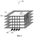
- FIG. 3shows a top view of a portion of one embodiment of a stacked package assembly 300 .
- stacking the flash memory devices on top of a flash interface circuitresults in a package with a very small volume.
- Various embodimentsmay be tested and burned in before assembly.
- the packagemay be manufactured using existing assembly infrastructure, tested in advance of stack assembly and require significantly less raw material, in some embodiments.
- Other embodimentsmay include a radial configuration, rather than a stack, or any other desired assembly.
- the electrical connections between flash memory devices and the flash interface circuitare generally around the edge of the physical perimeter of the devices.
- the connectionsmay be made through the devices, using through-wafer interconnect (TWI), for example.
- TWIthrough-wafer interconnect
- the flash interface circuitmay be integrated with one or more flash devices onto a single monolithic semiconductor die.
- FIG. 4shows a view of a die 400 including one or more flash memory circuits 410 and one or more flash interface circuits 420 .
- flash interface circuit 500includes an electrical interface to the host system 501 , an electrical interface to the flash memory device(s) 502 , configuration logic 503 , a configuration block 504 , a read-only memory (ROM) block 505 , a flash discovery block 506 , discovery logic 507 , an address translation unit 508 , and a unit for translations other than address translations 509 .
- the electrical interface to the flash memory devices(s) 502is coupled to the address translation unit 508 , the other translations unit 509 , and the L signals to the flash memory devices (e.g. as illustrated in FIG. 1 ). That is, the electrical interface 502 comprises the circuitry to drive and/or receive signals to/from the flash memory devices.
- the electrical interface to the host system 501is coupled to the other translations unit 509 , the address translation unit 508 , and the signals to the host interface (S in FIG. 5 ). That is, the electrical interface 501 comprises the circuitry to drive and/or receive signals to/from the host system.
- the discovery logic 507is coupled to the configuration logic 503 , and one or both of logic 507 and 503 is coupled to the other translations unit 509 and the address translation unit 508 .
- the flash discovery block 506is coupled to the discovery logic 507 , and the configuration block 504 and the ROM block 505 are coupled to the configuration logic 503 .
- the logic 503 and 507 and the translation units 508 and 509may be implemented in any desired fashion (combinatorial logic circuitry, pipelined circuitry, processor-based software, state machines, various other circuitry, and/or any combination of the foregoing).
- the blocks 504 , 506 , and 508may comprise any storage circuitry (e.g. register files, random access memory, etc.).
- the translation units 508 and 509may translate host flash memory access and configuration requests into requests to one or more flash memory devices, and may translate flash memory replies to host system replies if needed. That is, the translation units 508 and 509 may be configured to modify requests provided from the host system based on differences between the virtual configuration presented by the interface circuit 500 to the host system and the physical configuration of the flash memory devices, as determined by the discovery logic 507 and/or the configuration logic 503 and stored in the configuration block 504 and/or the discovery block 506 .
- the configuration block 504 , the ROM block 505 , and/or the flash discovery block 506may store data identifying the physical and virtual configurations.
- the discovery (or auto configuration) techniquemay be selected using an auto configuration signal mentioned previously (e.g. strapping the signal to an active level, either high or low).
- Fixed configuration informationmay be programmed into the ROM block 505 , in another technique. The selection of this technique may be implemented by strapping the auto configuration signal to an inactive level.
- the configuration block (CB) 504stores the virtual configuration.
- the configurationmay be set during the discovery process, or may be loaded from ROM block 505 .
- the ROM block 505may store configuration data for the flash memory devices and/or configuration data for the virtual configuration.
- the flash discovery block (FB) 306may store configuration data discovered from attached flash memory devices. In one embodiment, if some information is not discoverable from attached flash memory devices, that information may be copied from ROM block 505 .
- the configuration block 504 , the ROM block 505 , and the discovery block 506may store configuration data in any desired format and may include any desired configuration data, in various embodiments. Exemplary configurations of the configuration block 504 , the ROM block 505 , and the discovery block 506 are illustrated in FIGS. 7 , 8 , and 9 , respectively.
- FIG. 7is a table 700 illustrating one embodiment of configuration data stored in one embodiment of a configuration block 504 .
- the configuration block 504may comprise one or more instances of the configuration data in table 700 for various attached flash devices and for the virtual configuration.
- the configuration datacomprises 8 bytes of attributes, labeled 0 to 7 in FIG. 7 and having various bit fields as shown in FIG. 7 .
- Byte zeroincludes a auto discover bit (AUTO), indicating whether or not auto discovery is used to identify the configuration data; an ONFI bit indicating if ONFI is supported; and a chips field (CHIPS) indicating how many chip selects are exposed (automatic, 1, 2, or 4 in this embodiment, although other variations are contemplated).
- AUTOauto discover bit
- ONFIONFI
- CHIPSchips field
- Byte oneis a code indicate the manufacturer (maker) of the device (or the maker reported to the host); and byte two is a device code identifying the particular device from that manufacturer.
- Byte threeincludes a chip number field (CIPN) indicating the number of chips that are internal to flash memory system (e.g. stacked with the flash interface circuit or integrated on the same substrate as the interface circuit, in some embodiments). Byte three also includes a cell field (CELL) identifying the cell type, for embodiments that support multilevel cells.
- the simultaneously programmed field (SIMP)indicates the number of simultaneously programmed pages for the flash memory system.
- the interleave bit (INTRL)indicates whether or not chip interleave is supported, and the cache bit (CACHE) indicates whether or not caching is supported.
- Byte fourincludes a page size field (PAGE), a redundancy size bit (RSIZE) indicating the amount of redundancy supported (e.g. 8 or 16 bytes of redundancy per 512 bytes, in this embodiment), bits (SMIN) indicating minimum timings for serial access, a block size field (BSIZE) indicating the block size, and an organization byte (ORG) indicating the data width organization (e.g. x8 or x16, in this embodiment, although other widths are contemplated).
- Byte fiveincludes plane number and plane size fields (PLANE and PLSIZE). Some fields and bytes are reserved for future expansion.
- multibit fieldsmay also be used (e.g. to support additional variations for the described attribute).
- a multibit fieldmay be implemented as a single bit if fewer variations are supported for the corresponding attribute.
- FIG. 8is a table 800 of one embodiment of configuration data stored in the ROM block 505 .
- the ROM block 505may comprise one or more instances of the configuration data in table 800 for various attached flash devices and for the configuration presented to the host system.
- the configuration datais a subset of the data stored in the configuration block. That is, bytes one to five are included. Byte 0 may be determined through discovery, and bytes 6 and 7 are reserved and therefore not needed in the ROM block 505 for this embodiment.
- FIG. 9is a table 900 of one embodiment of configuration data that may be stored in the discovery block 506 .
- the discovery block 506may comprise one or more instances of the configuration data in table 900 for various attached flash devices.
- the configuration datais a subset of the data stored in the configuration block. That is, bytes zero to five are included (except for the AUTO bit, which is implied as a one in this case). Bytes 6 and 7 are reserved and therefore not needed in the discovery block 506 for this embodiment.
- the discovery informationis discovered using one or more read operations to the attached flash memory devices, initiated by the discovery logic 507 .
- a read cyclemay be used to test if ONFI is enabled for one or more of the attached devices.
- the test resultsmay be recorded in the ONFI bit of the discovery block.
- Another read cycle or cyclesmay test for the number of flash chips; and the result may be recorded in the CHIPS field.
- Remaining attributesmay be discovered by reading the ID definition table in the attached devices.
- the attached flash chipsmay have the same attributes.
- multiple instances of the configuration datamay be stored in the discovery block 506 and various attached flash memory devices may have differing attributes.
- the address translation unit 508may translate addresses between the host and the flash memory devices.
- the minimum page sizeis 1 kilobyte (KB).
- the page sizeis 8 KB.
- the page sizeis 2 KB.
- the address bitsmay be transmitted to the flash interface circuit over several transfers (e.g. 5 transfers, in one embodiment).
- the first two transferscomprise the address bits for the column address, low order address bits first (e.g. 11 bits for a 1 KB page up to 14 bits for an 8 KB page).
- the last three transferscomprise the row address, low order bits first.
- an internal address format for the flash interface circuitcomprises a valid bit indicating whether or not a request is being transmitted; a device field identifying the addressed flash memory device; a plane field identifying a plane within the device, a block field identifying the block number within the plane; a page number identifying a page within the block; a redundant bit indicating whether or not the redundant area is being addressed, and column address field containing the column address.
- a host addressis translated to the internal address format according the following rules (where CB_[label] corresponds to fields in FIG. 7 ):
- the translation from the internal address format to an address to be transmitted to the attached flash devicesmay be performed according to the following rules (where CB_[label] corresponds to fields in FIG. 9 ):
- Other translations that may be performed by the other translations unit 509may include a test to ensure that the amount of configured memory reported to the host is the same as or less than the amount of physically-attached memory. Addition, if the configured page size reported to the host is different than the discovered page size in the attached devices, a translation may be performed by the other translations unit 509 . For example, if the configured page size is larger than the discovered page size, the memory request may be performed to multiple flash memory devices to form a page of the configured size. If the configured page size is larger than the discovered page size multiplied by the number of flash memory devices, the request may be performed as multiple operations to multiple pages on each device to form a page of the configured size.
- the other translation unit 509may concatenate two blocks and their redundant areas. If the organization reported to the host is narrower than the organization of the attached devices, the translation unit 509 may select a byte or bytes from the data provided by the attached devices to be output as the data for the request.
- some or all signals of a multi-level cell (MLC) flash device 603pass through a flash interface circuit 602 disposed between the MLC flash device and the system 601 .
- the flash interface circuitpresents to the system as a single level cell (SLC)-type flash memory device.
- SLCsingle level cell
- the values representative of an SLC-type flash memory deviceappear coded into a configuration block that is presented to the system.
- some MLC signalsare presented to the system 601 .
- all MLC signalsare received by the flash interface circuit 602 and are converted to SLC signals for interface to the system 601 .
- one of more flash memory chips and one of more flash interface circuitsmay or may not be capable of operating from the same supply voltage. If, for example, the supply voltages of portion(s) the flash memory and portions(s) flash interface circuit are different, there are many techniques for either translating the supply voltage and/or translating the logic levels of the interconnecting signals. For example, since the supply currents required for portion(s) (e.g. core logic circuits, etc.) of the flash memory and/or portion(s) (e.g. core logic circuits, etc.) of the flash interface circuit may be relatively low (e.g.
- a resistorused as a voltage conversion resistor
- a switching voltage regulatormay be used to translate supply voltage levels.
- the I/O transistorsas logic transistors, thus eliminating the need for voltage translation.
- a relatively older process technologye.g.
- 0.25 micron, 0.35 micron, etcmay be employed for the flash interface circuit compared to the technology of the flash memory (e.g. 70 nm, 110 nm, etc.). Or in another embodiment a process that provides transistors that are capable of operating at multiple supply voltages may be employed.
- FIG. 10is a flowchart illustrating one embodiment of a method of emulating one or more virtual flash memory devices using one or more physical flash memory devices having at least one differing attribute. The method may be implemented, e.g., in the flash interface circuit embodiments described herein.
- the flash interface circuitmay wait for the host system to attempt flash discovery (decision block 1001 ).
- the flash interface circuitmay perform device discovery/configuration for the physical flash memory devices coupled to the flash interface circuit (block 1002 ).
- the flash interface circuitmay configure the physical flash memory devices before receiving the host discovery request.
- the flash interface circuitmay determine the virtual configuration based on the discovered flash memory devices and/or other data (e.g. ROM data) (block 1003 ).
- the flash interface circuitmay report the virtual configuration to the host (block 1004 ), thus exposing the virtual configuration to the host rather than the physical configuration.
- the flash interface circuitmay translate the request into one or more physical flash memory device accesses (block 1006 ), emulate attributes of the virtual configuration that differ from the physical flash memory devices (block 1007 ), and return an appropriate response to the request to the host (block 1008 ).
- the flash memory controllermay be part of the host system, in one embodiment (e.g. the flash memory controller 108 shown in FIG. 1 ). That is, the flash interface circuit may be between the flash memory controller and the flash memory devices (although some signals may be directly coupled between the system and the flash memory devices, e.g. as shown in FIG. 1 ).
- certain small processors for embedded applicationsmay include a flash memory interface.
- larger systemsmay include a flash memory interface in a chipset, such as in a bus bridge or other bridge device.
- an interface circuitmay be configured to couple to one or more flash memory devices and may be further configured to couple to a host system.
- the interface circuitis configured to present at least one virtual flash memory device to the host system, and the interface circuit is configured to implement the virtual flash memory device using the one or more flash memory devices to which the interface circuit is coupled.
- the virtual flash memory devicediffers from the one or more flash memory devices in at least one aspect (or attribute).
- the interface circuitis configured to translate a protocol implemented by the host system to a protocol implemented by the one or more flash memory devices, and the interface circuit may further be configured to translate the protocol implemented by the one or more flash memory devices to the protocol implemented by the host system.
- Either protocolmay be a NAND protocol or a NOR protocol, in some embodiments.
- the virtual flash memory deviceis pin-compatible with a standard pin interface and the one or more flash memories are not pin-compatible with the standard pin interface.
- the interface circuitfurther comprises at least one error detection circuit configured to detect errors in data from the one or more flash memory devices.
- the interface circuitmay still further comprise at least one error correction circuit configured to correct a detected error prior to forwarding the data to the host system.
- the interface circuitis configured to implement wear leveling operations in the one or more flash memory devices.
- the interface circuitcomprises a prefetch circuit configured to generate one or more prefetch operations to read data from the one or more flash memory devices.
- the virtual flash memory devicecomprises a data bus having a width equal to N times a width of a data bus of any one of the one or more flash devices, wherein N is an integer greater than one.
- the interface circuitis configured to interleave data on the buses of the one or more flash memory devices to implement the data bus of the virtual flash memory device.
- the interface circuitis configured to operate the data buses of the one or more flash memory devices in parallel to implement the data bus of the virtual flash memory device.
- the virtual flash memory devicehas a bandwidth that exceeds a bandwidth of the one or more flash memory devices.
- the virtual flash memory devicehas a latency that is less than the latency of the one or more flash memory devices.
- the flash memory deviceis a multi-level cell (MLC) flash device, and the virtual flash memory device presented to the host system is a single-level cell (SLC) flash device.
- MLCmulti-level cell
- SLCsingle-level cell
Landscapes
- Engineering & Computer Science (AREA)
- Theoretical Computer Science (AREA)
- Physics & Mathematics (AREA)
- General Engineering & Computer Science (AREA)
- General Physics & Mathematics (AREA)
- Human Computer Interaction (AREA)
- Techniques For Improving Reliability Of Storages (AREA)
Abstract
Description
| COL[7:0] = Cycle[1][7:0]; |
| COL[12:8] = Cycle[2][4:0]; |
| R = CB_PAGE == 0 ? Cycle[2][2] |
| : CB _PAGE == 1 ? | Cycle[2][3] |
| : CB _PAGE == 2 ? | Cycle[2][4] |
| : | Cycle[2][5]; |
| // block 64,128,256,512K / |
| PW[2:0] = CB_BSIZE == 0 && CB_PAGE == 0 ? | 6-6 | // | 0 |
| : CB_BSIZE == 0 && CB_PAGE == 1 ? | 5-6 | // | −1 |
| : CB_BSIZE == 0 && CB_PAGE == 2 ? | 4-6 | // | −2 |
| : CB_BSIZE == 0 && CB_PAGE == 3 ? | 3-6 | // | −3 |
| : CB_BSIZE == 1 && CB_PAGE == 0 ? | 7-6 | // | 1 |
| : CB_BSIZE == 1 && CB_PAGE == 1 ? | 6-6 | // | 0 |
| : CB_BSIZE == 1 && CB_PAGE == 2 ? | 5-6 | // | −1 |
| : CB_BSIZE == 1 && CB_PAGE == 3 ? | 4-6 | // | −2 |
| : CB_BSIZE == 2 && CB_PAGE == 0 ? | 8-6 | // | 2 |
| : CB_BSIZE == 2 && CB_PAGE == 1 ? | 7-6 | // | 1 |
| : CB_BSIZE == 2 && CB_PAGE == 2 ? | 6-6 | // | 0 |
| : CB_BSIZE == 2 && CB_PAGE == 3 ? | 5-6 | // | −1 |
| : CB_BSIZE == 3 && CB_PAGE == 0 ? | 9-6 | // | 3 |
| : CB_BSIZE == 3 && CB_PAGE == 1 ? | 8-6 | // | 2 |
| : CB_BSIZE == 3 && CB_PAGE == 2 ? | 7-6 | // | 1 |
| : | 6-6; | // | 0 |
| PW[2:0] = CB_BSIZE - CB_PAGE; | // | same | |
| as | |||
| above |
| PAGE = PW == −3 ? {5′b0, Cycle[3][2:0]} |
| : PW == −2 ? | {4′b0, | Cycle[3][3:0]} |
| : PW == −1 ? | {3′b0, | Cycle[3][4:0]} |
| : PW == 0 ? | {2′b0, | Cycle[3][5:0]} |
| : PW == 1 ? | {1′b0, | Cycle[3][6:0]} |
| : PW == 2 ? | { | Cycle[3][7:0]} |
| : | {Cycle[4][0], | Cycle[3][7:0]}; |
| BLOCK = PW == −3 ? { Cycle[5], Cycle[4], Cycle[3][7:3]} |
| : PW == −2 ? | {1′b0, Cycle[5], Cycle[4], Cycle[3][7:4]} |
| : PW == −1 ? | {2′b0, Cycle[5], Cycle[4], Cycle[3][7:5]} |
| : PW == 0 ? | {3′b0, Cycle[5], Cycle[4], Cycle[3][7:6]} |
| : PW == 1 ? | {4′b0, Cycle[5], Cycle[4], Cycle[3][7:7]} |
| : PW == 2 ? | {5′b0, Cycle[5], Cycle[4]} |
| : | {6′b0, Cycle[5], Cycle[4][7:1]}; |
| // CB_PLSIZE 64Mb = 0 .. 8Gb = 7 or 8MB .. 1GB |
| PB[3:0] = CB_PLSIZE - CB_PAGE; // PLANE_SIZE / PAGE_SIZE |
| PLANE = PB == −3 ? {10′b0, BLOCK[20:11]} |
| : PB == −2 ? | { 9′b0, | BLOCK[20:10]} |
| : PB == −1 ? | { 8′b0, | BLOCK[20: 9]} |
| : PB == 0 ? | { 7′b0, | BLOCK[20: 8]} |
| : PB == 1 ? | { 6′b0, | BLOCK[20: 7]} |
| : PB == 2 ? | { 5′b0, | BLOCK[20: 6]} |
| : PB == 3 ? | { 4′b0, | BLOCK[20: 5]} |
| : PB == 4 ? | { 3′b0, | BLOCK[20: 4]} |
| : PB == 5 ? | { 2′b0, | BLOCK[20: 3]} |
| : PB == 6 ? | { 1′b0, | BLOCK[20: 2]} |
| : | { | BLOCK[20: 1]}; |
| DEV = CE1_ == 1′b0 ? 2′ |
| : CE2_ == 1′b0 ? 2′d 1 |
| : CE3_ == 1′b0 ? 2′d 2 |
| : CE4_ == 1′b0 ? 2′d 3 |
| : 2′ |
| Cycle[1][7:0] = COL[7:0]; | |
| Cycle[2][7:0] = FB_PAGE == 0 ? {5′b0, R, COL[ 9:8]} | |
| : FB_PAGE == 1 ? | {4′b0, R, COL[10:8]} | |
| : FB_PAGE == 2 ? | {3′b0, R, COL[11:8]} | |
| : | {2′b0, R, COL[12:8]}; |
| Cycle[3][7:0] = PAGE[7:0]; | |
| Cycle[3][0] = PAGE[8]; | |
| BLOCK[ ] = CB_PAGE == 0 ? Cycle [ ][ ] : | |
| CB_PAGE == 1 ? Cycle [ ][ ] : | |
| CB_PAGE == 2 ? Cycle [ ][ ] : |
| Cycle [ ][ ] : ; |
| PLANE = TBD | |
| FCE1_ = !(DEV == 0 && VALID); | |
| FCE2_ = !(DEV == 1 && VALID); | |
| FCE3_ = !(DEV == 2 && VALID); | |
| FCE4_ = !(DEV == 3 && VALID); | |
| FCE5_ = !(DEV == 4 && VALID); | |
| FCE6_ = !(DEV == 5 && VALID); | |
| FCE7_ = !(DEV == 6 && VALID); | |
| FCE8_ = !(DEV == 7 && VALID); | |
Claims (20)
Priority Applications (4)
| Application Number | Priority Date | Filing Date | Title |
|---|---|---|---|
| US13/620,424US8751732B2 (en) | 2006-10-05 | 2012-09-14 | System and method for increasing capacity, performance, and flexibility of flash storage |
| US14/090,342US9171585B2 (en) | 2005-06-24 | 2013-11-26 | Configurable memory circuit system and method |
| US14/922,388US9507739B2 (en) | 2005-06-24 | 2015-10-26 | Configurable memory circuit system and method |
| US15/358,335US10013371B2 (en) | 2005-06-24 | 2016-11-22 | Configurable memory circuit system and method |
Applications Claiming Priority (4)
| Application Number | Priority Date | Filing Date | Title |
|---|---|---|---|
| US84963106P | 2006-10-05 | 2006-10-05 | |
| US11/611,374US8055833B2 (en) | 2006-10-05 | 2006-12-15 | System and method for increasing capacity, performance, and flexibility of flash storage |
| US13/276,212US8370566B2 (en) | 2006-10-05 | 2011-10-18 | System and method for increasing capacity, performance, and flexibility of flash storage |
| US13/620,424US8751732B2 (en) | 2006-10-05 | 2012-09-14 | System and method for increasing capacity, performance, and flexibility of flash storage |
Related Parent Applications (1)
| Application Number | Title | Priority Date | Filing Date |
|---|---|---|---|
| US13/276,212ContinuationUS8370566B2 (en) | 2005-06-24 | 2011-10-18 | System and method for increasing capacity, performance, and flexibility of flash storage |
Related Child Applications (2)
| Application Number | Title | Priority Date | Filing Date |
|---|---|---|---|
| US11/611,374Continuation-In-PartUS8055833B2 (en) | 2005-06-24 | 2006-12-15 | System and method for increasing capacity, performance, and flexibility of flash storage |
| US14/090,342Continuation-In-PartUS9171585B2 (en) | 2005-06-24 | 2013-11-26 | Configurable memory circuit system and method |
Publications (2)
| Publication Number | Publication Date |
|---|---|
| US20130132645A1 US20130132645A1 (en) | 2013-05-23 |
| US8751732B2true US8751732B2 (en) | 2014-06-10 |
Family
ID=39275845
Family Applications (3)
| Application Number | Title | Priority Date | Filing Date |
|---|---|---|---|
| US11/611,374Active2028-01-12US8055833B2 (en) | 2005-06-24 | 2006-12-15 | System and method for increasing capacity, performance, and flexibility of flash storage |
| US13/276,212ActiveUS8370566B2 (en) | 2005-06-24 | 2011-10-18 | System and method for increasing capacity, performance, and flexibility of flash storage |
| US13/620,424ActiveUS8751732B2 (en) | 2005-06-24 | 2012-09-14 | System and method for increasing capacity, performance, and flexibility of flash storage |
Family Applications Before (2)
| Application Number | Title | Priority Date | Filing Date |
|---|---|---|---|
| US11/611,374Active2028-01-12US8055833B2 (en) | 2005-06-24 | 2006-12-15 | System and method for increasing capacity, performance, and flexibility of flash storage |
| US13/276,212ActiveUS8370566B2 (en) | 2005-06-24 | 2011-10-18 | System and method for increasing capacity, performance, and flexibility of flash storage |
Country Status (1)
| Country | Link |
|---|---|
| US (3) | US8055833B2 (en) |
Cited By (8)
| Publication number | Priority date | Publication date | Assignee | Title |
|---|---|---|---|---|
| US8930647B1 (en) | 2011-04-06 | 2015-01-06 | P4tents1, LLC | Multiple class memory systems |
| US9158546B1 (en) | 2011-04-06 | 2015-10-13 | P4tents1, LLC | Computer program product for fetching from a first physical memory between an execution of a plurality of threads associated with a second physical memory |
| US9164679B2 (en) | 2011-04-06 | 2015-10-20 | Patents1, Llc | System, method and computer program product for multi-thread operation involving first memory of a first memory class and second memory of a second memory class |
| US9170744B1 (en) | 2011-04-06 | 2015-10-27 | P4tents1, LLC | Computer program product for controlling a flash/DRAM/embedded DRAM-equipped system |
| US9176671B1 (en) | 2011-04-06 | 2015-11-03 | P4tents1, LLC | Fetching data between thread execution in a flash/DRAM/embedded DRAM-equipped system |
| US9417754B2 (en) | 2011-08-05 | 2016-08-16 | P4tents1, LLC | User interface system, method, and computer program product |
| US10355001B2 (en)* | 2012-02-15 | 2019-07-16 | Micron Technology, Inc. | Memories and methods to provide configuration information to controllers |
| US10438253B2 (en) | 2015-11-29 | 2019-10-08 | International Business Machines Corporation | Reuse of computing resources for cloud managed services |
Families Citing this family (82)
| Publication number | Priority date | Publication date | Assignee | Title |
|---|---|---|---|---|
| US8335894B1 (en) | 2008-07-25 | 2012-12-18 | Google Inc. | Configurable memory system with interface circuit |
| US9542352B2 (en) | 2006-02-09 | 2017-01-10 | Google Inc. | System and method for reducing command scheduling constraints of memory circuits |
| US20080082763A1 (en) | 2006-10-02 | 2008-04-03 | Metaram, Inc. | Apparatus and method for power management of memory circuits by a system or component thereof |
| KR101377305B1 (en)* | 2005-06-24 | 2014-03-25 | 구글 인코포레이티드 | An integrated memory core and memory interface circuit |
| US8041881B2 (en) | 2006-07-31 | 2011-10-18 | Google Inc. | Memory device with emulated characteristics |
| US8438328B2 (en) | 2008-02-21 | 2013-05-07 | Google Inc. | Emulation of abstracted DIMMs using abstracted DRAMs |
| US20080028136A1 (en) | 2006-07-31 | 2008-01-31 | Schakel Keith R | Method and apparatus for refresh management of memory modules |
| US9171585B2 (en) | 2005-06-24 | 2015-10-27 | Google Inc. | Configurable memory circuit system and method |
| US8060774B2 (en) | 2005-06-24 | 2011-11-15 | Google Inc. | Memory systems and memory modules |
| US8077535B2 (en) | 2006-07-31 | 2011-12-13 | Google Inc. | Memory refresh apparatus and method |
| US8130560B1 (en) | 2006-11-13 | 2012-03-06 | Google Inc. | Multi-rank partial width memory modules |
| US10013371B2 (en) | 2005-06-24 | 2018-07-03 | Google Llc | Configurable memory circuit system and method |
| US8090897B2 (en) | 2006-07-31 | 2012-01-03 | Google Inc. | System and method for simulating an aspect of a memory circuit |
| US9507739B2 (en) | 2005-06-24 | 2016-11-29 | Google Inc. | Configurable memory circuit system and method |
| US8089795B2 (en) | 2006-02-09 | 2012-01-03 | Google Inc. | Memory module with memory stack and interface with enhanced capabilities |
| US8081474B1 (en) | 2007-12-18 | 2011-12-20 | Google Inc. | Embossed heat spreader |
| US8244971B2 (en) | 2006-07-31 | 2012-08-14 | Google Inc. | Memory circuit system and method |
| US8397013B1 (en) | 2006-10-05 | 2013-03-12 | Google Inc. | Hybrid memory module |
| US8111566B1 (en) | 2007-11-16 | 2012-02-07 | Google, Inc. | Optimal channel design for memory devices for providing a high-speed memory interface |
| US8796830B1 (en) | 2006-09-01 | 2014-08-05 | Google Inc. | Stackable low-profile lead frame package |
| US8359187B2 (en) | 2005-06-24 | 2013-01-22 | Google Inc. | Simulating a different number of memory circuit devices |
| US8386722B1 (en) | 2008-06-23 | 2013-02-26 | Google Inc. | Stacked DIMM memory interface |
| US8327104B2 (en) | 2006-07-31 | 2012-12-04 | Google Inc. | Adjusting the timing of signals associated with a memory system |
| US7609567B2 (en) | 2005-06-24 | 2009-10-27 | Metaram, Inc. | System and method for simulating an aspect of a memory circuit |
| US8055833B2 (en) | 2006-10-05 | 2011-11-08 | Google Inc. | System and method for increasing capacity, performance, and flexibility of flash storage |
| US7386656B2 (en) | 2006-07-31 | 2008-06-10 | Metaram, Inc. | Interface circuit system and method for performing power management operations in conjunction with only a portion of a memory circuit |
| WO2007028109A2 (en) | 2005-09-02 | 2007-03-08 | Metaram, Inc. | Methods and apparatus of stacking drams |
| US9632929B2 (en) | 2006-02-09 | 2017-04-25 | Google Inc. | Translating an address associated with a command communicated between a system and memory circuits |
| US7724589B2 (en) | 2006-07-31 | 2010-05-25 | Google Inc. | System and method for delaying a signal communicated from a system to at least one of a plurality of memory circuits |
| US20080155151A1 (en)* | 2006-12-22 | 2008-06-26 | International Business Machines Corporation | Programmable Locking Mechanism For Secure Applications In An Integrated Circuit |
| US20080155175A1 (en)* | 2006-12-26 | 2008-06-26 | Sinclair Alan W | Host System That Manages a LBA Interface With Flash Memory |
| KR100936149B1 (en)* | 2006-12-29 | 2010-01-12 | 삼성전자주식회사 | Memory system having a plurality of nonvolatile memories, its memory access method |
| JP4781373B2 (en)* | 2007-05-14 | 2011-09-28 | 株式会社バッファロー | Storage device |
| US7979627B2 (en)* | 2007-05-14 | 2011-07-12 | Buffalo Inc. | Storage device with binary and multivalued memory |
| US7747903B2 (en)* | 2007-07-09 | 2010-06-29 | Micron Technology, Inc. | Error correction for memory |
| US8209479B2 (en) | 2007-07-18 | 2012-06-26 | Google Inc. | Memory circuit system and method |
| US8080874B1 (en) | 2007-09-14 | 2011-12-20 | Google Inc. | Providing additional space between an integrated circuit and a circuit board for positioning a component therebetween |
| US9152496B2 (en)* | 2007-12-21 | 2015-10-06 | Cypress Semiconductor Corporation | High performance flash channel interface |
| JP5063337B2 (en) | 2007-12-27 | 2012-10-31 | 株式会社日立製作所 | Semiconductor device |
| US8068365B2 (en) | 2008-02-04 | 2011-11-29 | Mosaid Technologies Incorporated | Non-volatile memory device having configurable page size |
| WO2009097681A1 (en)* | 2008-02-04 | 2009-08-13 | Mosaid Technologies Incorporated | Flexible memory operations in nand flash devices |
| KR101103110B1 (en) | 2008-02-29 | 2012-01-04 | 가부시끼가이샤 도시바 | Memory system |
| JP5010505B2 (en)* | 2008-03-01 | 2012-08-29 | 株式会社東芝 | Memory system |
| US20090327535A1 (en)* | 2008-06-30 | 2009-12-31 | Liu Tz-Yi | Adjustable read latency for memory device in page-mode access |
| US8412880B2 (en) | 2009-01-08 | 2013-04-02 | Micron Technology, Inc. | Memory system controller to manage wear leveling across a plurality of storage nodes |
| DE202010017690U1 (en) | 2009-06-09 | 2012-05-29 | Google, Inc. | Programming dimming terminating resistor values |
| US8909831B2 (en)* | 2009-11-27 | 2014-12-09 | International Business Machines Corporation | Logic device |
| US20120179883A1 (en)* | 2011-01-12 | 2012-07-12 | Broadcom Corpotation | System and method for dynamically adjusting memory performance |
| US9318166B2 (en) | 2011-07-22 | 2016-04-19 | SanDisk Technologies, Inc. | Systems and methods of storing data |
| US20130282962A1 (en)* | 2012-04-20 | 2013-10-24 | SMART Storage Systems, Inc. | Storage control system with flash configuration and method of operation thereof |
| TWI467379B (en)* | 2012-04-23 | 2015-01-01 | Phison Electronics Corp | System operation method, and memory controller and memory storage device using the same |
| US20140032820A1 (en)* | 2012-07-25 | 2014-01-30 | Akinori Harasawa | Data storage apparatus, memory control method and electronic device with data storage apparatus |
| US9235528B2 (en)* | 2012-12-21 | 2016-01-12 | Advanced Micro Devices, Inc. | Write endurance management techniques in the logic layer of a stacked memory |
| TWI456393B (en)* | 2012-12-24 | 2014-10-11 | Phison Electronics Corp | Data reading method, memory controller and memory storage device |
| US11249652B1 (en) | 2013-01-28 | 2022-02-15 | Radian Memory Systems, Inc. | Maintenance of nonvolatile memory on host selected namespaces by a common memory controller |
| US9652376B2 (en) | 2013-01-28 | 2017-05-16 | Radian Memory Systems, Inc. | Cooperative flash memory control |
| US9229854B1 (en) | 2013-01-28 | 2016-01-05 | Radian Memory Systems, LLC | Multi-array operation support and related devices, systems and software |
| US10445229B1 (en) | 2013-01-28 | 2019-10-15 | Radian Memory Systems, Inc. | Memory controller with at least one address segment defined for which data is striped across flash memory dies, with a common address offset being used to obtain physical addresses for the data in each of the dies |
| US10642505B1 (en) | 2013-01-28 | 2020-05-05 | Radian Memory Systems, Inc. | Techniques for data migration based on per-data metrics and memory degradation |
| CN104981872B (en)* | 2013-03-15 | 2018-11-06 | 英特尔公司 | Storage system |
| US20140372666A1 (en)* | 2013-06-14 | 2014-12-18 | Ps4 Luxco S.A.R.L. | Semiconductor device with configurable support for multiple command specifications, and method regarding the same |
| US10552085B1 (en) | 2014-09-09 | 2020-02-04 | Radian Memory Systems, Inc. | Techniques for directed data migration |
| US9542118B1 (en) | 2014-09-09 | 2017-01-10 | Radian Memory Systems, Inc. | Expositive flash memory control |
| US10073627B2 (en)* | 2015-01-13 | 2018-09-11 | Sandisk Technologies Llc | Addressing, interleave, wear leveling, and initialization schemes for different chip enables and memory arrays of different types |
| CN104794011B (en)* | 2015-02-04 | 2017-12-12 | 深圳神州数码云科数据技术有限公司 | Bad block reorientation method and device based on virtual disk |
| CN106155912A (en)* | 2015-04-14 | 2016-11-23 | 扬智科技股份有限公司 | Multi-channel memory and memory access method thereof |
| US10552058B1 (en) | 2015-07-17 | 2020-02-04 | Radian Memory Systems, Inc. | Techniques for delegating data processing to a cooperative memory controller |
| US10037163B2 (en)* | 2015-07-29 | 2018-07-31 | Sandisk Technologies Llc | Self-describing cluster association |
| US9983829B2 (en)* | 2016-01-13 | 2018-05-29 | Sandisk Technologies Llc | Physical addressing schemes for non-volatile memory systems employing multi-die interleave schemes |
| CN109416656B (en) | 2016-10-31 | 2023-08-11 | 拉姆伯斯公司 | Hybrid memory module |
| US10268387B2 (en)* | 2017-01-04 | 2019-04-23 | Sandisk Technologies Llc | Meta-groups in non-volatile storage based on performance times |
| US11294440B2 (en) | 2017-11-17 | 2022-04-05 | Hewlett-Packard Development Company, L.P. | Peripheral device configurations by host systems |
| US10642747B1 (en)* | 2018-05-10 | 2020-05-05 | Seagate Technology Llc | Virtual flash system |
| US10585615B1 (en) | 2018-05-10 | 2020-03-10 | Seagate Technology Llc | Virtual flash system |
| US10871906B2 (en) | 2018-09-28 | 2020-12-22 | Intel Corporation | Periphery shoreline augmentation for integrated circuits |
| KR20200042780A (en)* | 2018-10-16 | 2020-04-24 | 에스케이하이닉스 주식회사 | Data storage device and operating method thereof |
| CN109445691B (en)* | 2018-10-16 | 2022-03-29 | 深圳忆联信息系统有限公司 | Method and device for improving FTL algorithm development and verification efficiency |
| KR20200114354A (en)* | 2019-03-28 | 2020-10-07 | 에스케이하이닉스 주식회사 | Memory system and operating method thereof |
| KR102743222B1 (en) | 2019-06-12 | 2024-12-17 | 삼성전자 주식회사 | Electronic device and method of utilizing storage space thereof |
| US11164847B2 (en) | 2019-12-03 | 2021-11-02 | Intel Corporation | Methods and apparatus for managing thermal behavior in multichip packages |
| US11175984B1 (en) | 2019-12-09 | 2021-11-16 | Radian Memory Systems, Inc. | Erasure coding techniques for flash memory |
| KR102733470B1 (en)* | 2023-08-30 | 2024-11-25 | 리벨리온 주식회사 | Chiplet system and method for communicating between chiplets in chiplet system |
Citations (705)
| Publication number | Priority date | Publication date | Assignee | Title |
|---|---|---|---|---|
| US1215561A (en) | 1914-01-21 | 1917-02-13 | Charles H Loew | Pasteurizer. |
| US3800292A (en) | 1972-10-05 | 1974-03-26 | Honeywell Inf Systems | Variable masking for segmented memory |
| US4069452A (en) | 1976-09-15 | 1978-01-17 | Dana Laboratories, Inc. | Apparatus for automatically detecting values of periodically time varying signals |
| US4323965A (en) | 1980-01-08 | 1982-04-06 | Honeywell Information Systems Inc. | Sequential chip select decode apparatus and method |
| US4334307A (en) | 1979-12-28 | 1982-06-08 | Honeywell Information Systems Inc. | Data processing system with self testing and configuration mapping capability |
| US4345319A (en) | 1978-06-28 | 1982-08-17 | Cselt-Centro Studi E Laboratori Telecomunicazioni S.P.A. | Self-correcting, solid-state-mass-memory organized by bits and with reconfiguration capability for a stored program control system |
| US4392212A (en) | 1979-11-12 | 1983-07-05 | Fujitsu Limited | Semiconductor memory device with decoder for chip selection/write in |
| EP0132129A2 (en) | 1983-07-14 | 1985-01-23 | BURROUGHS CORPORATION (a Michigan corporation) | Address translation buffer |
| US4500958A (en) | 1982-04-21 | 1985-02-19 | Digital Equipment Corporation | Memory controller with data rotation arrangement |
| US4525921A (en) | 1981-07-13 | 1985-07-02 | Irvine Sensors Corporation | High-density electronic processing package-structure and fabrication |
| US4566082A (en) | 1983-03-23 | 1986-01-21 | Tektronix, Inc. | Memory pack addressing system |
| US4592019A (en) | 1983-08-31 | 1986-05-27 | At&T Bell Laboratories | Bus oriented LIFO/FIFO memory |
| US4628407A (en) | 1983-04-22 | 1986-12-09 | Cray Research, Inc. | Circuit module with enhanced heat transfer and distribution |
| US4646128A (en) | 1980-09-16 | 1987-02-24 | Irvine Sensors Corporation | High-density electronic processing package--structure and fabrication |
| US4698748A (en) | 1983-10-07 | 1987-10-06 | Essex Group, Inc. | Power-conserving control system for turning-off the power and the clocking for data transactions upon certain system inactivity |
| US4706166A (en) | 1986-04-25 | 1987-11-10 | Irvine Sensors Corporation | High-density electronic modules--process and product |
| US4710903A (en) | 1986-03-31 | 1987-12-01 | Wang Laboratories, Inc. | Pseudo-static memory subsystem |
| US4764846A (en) | 1987-01-05 | 1988-08-16 | Irvine Sensors Corporation | High density electronic package comprising stacked sub-modules |
| US4780843A (en) | 1983-11-07 | 1988-10-25 | Motorola, Inc. | Wait mode power reduction system and method for data processor |
| US4794597A (en) | 1986-03-28 | 1988-12-27 | Mitsubishi Denki Kabushiki Kaisha | Memory device equipped with a RAS circuit |
| US4796232A (en) | 1987-10-20 | 1989-01-03 | Contel Corporation | Dual port memory controller |
| US4807191A (en) | 1988-01-04 | 1989-02-21 | Motorola, Inc. | Redundancy for a block-architecture memory |
| US4841440A (en) | 1983-04-26 | 1989-06-20 | Nec Corporation | Control processor for controlling a peripheral unit |
| US4862347A (en) | 1986-04-22 | 1989-08-29 | International Business Machine Corporation | System for simulating memory arrays in a logic simulation machine |
| US4884237A (en) | 1984-03-28 | 1989-11-28 | International Business Machines Corporation | Stacked double density memory module using industry standard memory chips |
| US4887240A (en) | 1987-12-15 | 1989-12-12 | National Semiconductor Corporation | Staggered refresh for dram array |
| US4888687A (en) | 1987-05-04 | 1989-12-19 | Prime Computer, Inc. | Memory control system |
| US4899107A (en) | 1988-09-30 | 1990-02-06 | Micron Technology, Inc. | Discrete die burn-in for nonpackaged die |
| US4912678A (en) | 1987-09-26 | 1990-03-27 | Mitsubishi Denki Kabushiki Kaisha | Dynamic random access memory device with staggered refresh |
| US4916575A (en) | 1988-08-08 | 1990-04-10 | Asten Francis C Van | Multiple circuit board module |
| US4922451A (en) | 1987-03-23 | 1990-05-01 | International Business Machines Corporation | Memory re-mapping in a microcomputer system |
| US4935734A (en) | 1985-09-11 | 1990-06-19 | Pilkington Micro-Electronics Limited | Semi-conductor integrated circuits/systems |
| US4937791A (en) | 1988-06-02 | 1990-06-26 | The California Institute Of Technology | High performance dynamic ram interface |
| US4956694A (en) | 1988-11-04 | 1990-09-11 | Dense-Pac Microsystems, Inc. | Integrated circuit chip stacking |
| US4982265A (en) | 1987-06-24 | 1991-01-01 | Hitachi, Ltd. | Semiconductor integrated circuit device and method of manufacturing the same |
| US4983533A (en) | 1987-10-28 | 1991-01-08 | Irvine Sensors Corporation | High-density electronic modules - process and product |
| US5025364A (en) | 1987-06-29 | 1991-06-18 | Hewlett-Packard Company | Microprocessor emulation system with memory mapping using variable definition and addressing of memory space |
| US5072424A (en) | 1985-07-12 | 1991-12-10 | Anamartic Limited | Wafer-scale integrated circuit memory |
| US5083266A (en) | 1986-12-26 | 1992-01-21 | Kabushiki Kaisha Toshiba | Microcomputer which enters sleep mode for a predetermined period of time on response to an activity of an input/output device |
| US5104820A (en) | 1989-07-07 | 1992-04-14 | Irvine Sensors Corporation | Method of fabricating electronic circuitry unit containing stacked IC layers having lead rerouting |
| US5193072A (en) | 1990-12-21 | 1993-03-09 | Vlsi Technology, Inc. | Hidden refresh of a dynamic random access memory |
| US5212666A (en) | 1989-07-10 | 1993-05-18 | Seiko Epson Corporation | Memory apparatus having flexibly designed memory capacity |
| US5220672A (en) | 1990-12-25 | 1993-06-15 | Mitsubishi Denki Kabushiki Kaisha | Low power consuming digital circuit device |
| US5222014A (en) | 1992-03-02 | 1993-06-22 | Motorola, Inc. | Three-dimensional multi-chip pad array carrier |
| US5241266A (en) | 1992-04-10 | 1993-08-31 | Micron Technology, Inc. | Built-in test circuit connection for wafer level burnin and testing of individual dies |
| US5252807A (en) | 1990-07-02 | 1993-10-12 | George Chizinsky | Heated plate rapid thermal processor |
| US5257233A (en) | 1990-10-31 | 1993-10-26 | Micron Technology, Inc. | Low power memory module using restricted RAM activation |
| US5278796A (en) | 1991-04-12 | 1994-01-11 | Micron Technology, Inc. | Temperature-dependent DRAM refresh circuit |
| US5282177A (en) | 1992-04-08 | 1994-01-25 | Micron Technology, Inc. | Multiple register block write method and circuit for video DRAMs |
| US5332922A (en) | 1990-04-26 | 1994-07-26 | Hitachi, Ltd. | Multi-chip semiconductor package |
| US5347428A (en) | 1992-12-03 | 1994-09-13 | Irvine Sensors Corporation | Module comprising IC memory stack dedicated to and structurally combined with an IC microprocessor chip |
| US5369749A (en) | 1989-05-17 | 1994-11-29 | Ibm Corporation | Method and apparatus for the direct transfer of information between application programs running on distinct processors without utilizing the services of one or both operating systems |
| US5384745A (en) | 1992-04-27 | 1995-01-24 | Mitsubishi Denki Kabushiki Kaisha | Synchronous semiconductor memory device |
| US5388265A (en) | 1992-03-06 | 1995-02-07 | Intel Corporation | Method and apparatus for placing an integrated circuit chip in a reduced power consumption state |
| US5390334A (en) | 1990-10-29 | 1995-02-14 | International Business Machines Corporation | Workstation power management by page placement control |
| US5390078A (en) | 1993-08-30 | 1995-02-14 | At&T Global Information Solutions Company | Apparatus for using an active circuit board as a heat sink |
| US5392251A (en) | 1993-07-13 | 1995-02-21 | Micron Semiconductor, Inc. | Controlling dynamic memory refresh cycle time |
| US5408190A (en) | 1991-06-04 | 1995-04-18 | Micron Technology, Inc. | Testing apparatus having substrate interconnect for discrete die burn-in for nonpackaged die |
| US5432729A (en) | 1993-04-23 | 1995-07-11 | Irvine Sensors Corporation | Electronic module comprising a stack of IC chips each interacting with an IC chip secured to the stack |
| EP0644547A3 (en) | 1993-09-13 | 1995-07-12 | Ibm | Integrated multichip memory module, structure and fabrication. |
| US5448511A (en) | 1994-06-01 | 1995-09-05 | Storage Technology Corporation | Memory stack with an integrated interconnect and mounting structure |
| US5453434A (en) | 1989-11-13 | 1995-09-26 | Allergan, Inc. | N-substituted derivatives of 3R,4R-ethyl-[(1-methyl-1H-imidazol-5-yl)methyl]-2-pyrrolidone |
| US5467455A (en) | 1993-11-03 | 1995-11-14 | Motorola, Inc. | Data processing system and method for performing dynamic bus termination |
| US5483497A (en) | 1993-08-24 | 1996-01-09 | Fujitsu Limited | Semiconductor memory having a plurality of banks usable in a plurality of bank configurations |
| US5498886A (en) | 1991-11-05 | 1996-03-12 | Monolithic System Technology, Inc. | Circuit module redundancy architecture |
| US5502333A (en) | 1994-03-30 | 1996-03-26 | International Business Machines Corporation | Semiconductor stack structures and fabrication/sparing methods utilizing programmable spare circuit |
| US5513339A (en) | 1992-09-30 | 1996-04-30 | At&T Corp. | Concurrent fault simulation of circuits with both logic elements and functional circuits |
| US5513135A (en) | 1994-12-02 | 1996-04-30 | International Business Machines Corporation | Synchronous memory packaged in single/dual in-line memory module and method of fabrication |
| US5519832A (en) | 1992-11-13 | 1996-05-21 | Digital Equipment Corporation | Method and apparatus for displaying module diagnostic results |
| US5526320A (en) | 1994-12-23 | 1996-06-11 | Micron Technology Inc. | Burst EDO memory device |
| US5530836A (en) | 1994-08-12 | 1996-06-25 | International Business Machines Corporation | Method and apparatus for multiple memory bank selection |
| US5550781A (en) | 1989-05-08 | 1996-08-27 | Hitachi Maxell, Ltd. | Semiconductor apparatus with two activating modes of different number of selected word lines at refreshing |
| US5559990A (en) | 1992-02-14 | 1996-09-24 | Advanced Micro Devices, Inc. | Memories with burst mode access |
| US5561622A (en) | 1993-09-13 | 1996-10-01 | International Business Machines Corporation | Integrated memory cube structure |
| US5566344A (en) | 1994-12-20 | 1996-10-15 | National Semiconductor Corporation | In-system programming architecture for a multiple chip processor |
| US5581498A (en) | 1993-08-13 | 1996-12-03 | Irvine Sensors Corporation | Stack of IC chips in lieu of single IC chip |
| US5590071A (en) | 1995-11-16 | 1996-12-31 | International Business Machines Corporation | Method and apparatus for emulating a high capacity DRAM |
| US5598376A (en) | 1994-12-23 | 1997-01-28 | Micron Technology, Inc. | Distributed write data drivers for burst access memories |
| US5604714A (en) | 1995-11-30 | 1997-02-18 | Micron Technology, Inc. | DRAM having multiple column address strobe operation |
| US5608262A (en) | 1995-02-24 | 1997-03-04 | Lucent Technologies Inc. | Packaging multi-chip modules without wire-bond interconnection |
| US5610864A (en) | 1994-12-23 | 1997-03-11 | Micron Technology, Inc. | Burst EDO memory device with maximized write cycle timing |
| US5627791A (en) | 1996-02-16 | 1997-05-06 | Micron Technology, Inc. | Multiple bank memory with auto refresh to specified bank |
| US5640337A (en) | 1992-07-10 | 1997-06-17 | Lsi Logic Corp. | Method and apparatus for interim in-situ testing of an electronic system with an inchoate ASIC |
| US5640364A (en) | 1994-12-23 | 1997-06-17 | Micron Technology, Inc. | Self-enabling pulse trapping circuit |
| US5652724A (en) | 1994-12-23 | 1997-07-29 | Micron Technology, Inc. | Burst EDO memory device having pipelined output buffer |
| US5654204A (en) | 1994-07-20 | 1997-08-05 | Anderson; James C. | Die sorter |
| US5661677A (en) | 1996-05-15 | 1997-08-26 | Micron Electronics, Inc. | Circuit and method for on-board programming of PRD Serial EEPROMS |
| US5668773A (en) | 1994-12-23 | 1997-09-16 | Micron Technology, Inc. | Synchronous burst extended data out DRAM |
| US5675549A (en) | 1994-12-23 | 1997-10-07 | Micron Technology, Inc. | Burst EDO memory device address counter |
| US5680342A (en) | 1996-04-10 | 1997-10-21 | International Business Machines Corporation | Memory module package with address bus buffering |
| US5682354A (en) | 1995-11-06 | 1997-10-28 | Micron Technology, Inc. | CAS recognition in burst extended data out DRAM |
| US5692202A (en) | 1995-12-29 | 1997-11-25 | Intel Corporation | System, apparatus, and method for managing power in a computer system |
| US5692121A (en) | 1995-04-14 | 1997-11-25 | International Business Machines Corporation | Recovery unit for mirrored processors |
| US5696929A (en) | 1995-10-03 | 1997-12-09 | Intel Corporation | Flash EEPROM main memory in a computer system |
| US5717654A (en) | 1995-02-10 | 1998-02-10 | Micron Technology, Inc. | Burst EDO memory device with maximized write cycle timing |
| USRE35733E (en) | 1991-11-26 | 1998-02-17 | Circuit Components Incorporated | Device for interconnecting integrated circuit packages to circuit boards |
| US5721859A (en) | 1994-12-23 | 1998-02-24 | Micron Technology, Inc. | Counter control circuit in a burst memory |
| US5724288A (en) | 1995-08-30 | 1998-03-03 | Micron Technology, Inc. | Data communication for memory |
| US5729504A (en) | 1995-12-14 | 1998-03-17 | Micron Technology, Inc. | Continuous burst edo memory device |
| US5729503A (en) | 1994-12-23 | 1998-03-17 | Micron Technology, Inc. | Address transition detection on a synchronous design |
| US5742792A (en) | 1993-04-23 | 1998-04-21 | Emc Corporation | Remote data mirroring |
| US5748914A (en) | 1995-10-19 | 1998-05-05 | Rambus, Inc. | Protocol for communication with dynamic memory |
| US5752045A (en) | 1995-07-14 | 1998-05-12 | United Microelectronics Corporation | Power conservation in synchronous SRAM cache memory blocks of a computer system |
| US5760478A (en) | 1996-08-20 | 1998-06-02 | International Business Machines Corporation | Clock skew minimization system and method for integrated circuits |
| US5761703A (en) | 1996-08-16 | 1998-06-02 | Unisys Corporation | Apparatus and method for dynamic memory refresh |
| US5765203A (en) | 1995-12-19 | 1998-06-09 | Seagate Technology, Inc. | Storage and addressing method for a buffer memory control system for accessing user and error imformation |
| US5781766A (en) | 1996-05-13 | 1998-07-14 | National Semiconductor Corporation | Programmable compensating device to optimize performance in a DRAM controller chipset |
| US5787457A (en) | 1996-10-18 | 1998-07-28 | International Business Machines Corporation | Cached synchronous DRAM architecture allowing concurrent DRAM operations |
| US5798961A (en) | 1994-08-23 | 1998-08-25 | Emc Corporation | Non-volatile memory module |
| US5802555A (en) | 1995-03-15 | 1998-09-01 | Texas Instruments Incorporated | Computer system including a refresh controller circuit having a row address strobe multiplexer and associated method |
| US5802395A (en) | 1996-07-08 | 1998-09-01 | International Business Machines Corporation | High density memory modules with improved data bus performance |
| US5818788A (en) | 1997-05-30 | 1998-10-06 | Nec Corporation | Circuit technique for logic integrated DRAM with SIMD architecture and a method for controlling low-power, high-speed and highly reliable operation |
| US5819065A (en) | 1995-06-28 | 1998-10-06 | Quickturn Design Systems, Inc. | System and method for emulating memory |
| US5831833A (en) | 1995-07-17 | 1998-11-03 | Nec Corporation | Bear chip mounting printed circuit board and a method of manufacturing thereof by photoetching |
| US5835435A (en) | 1997-12-02 | 1998-11-10 | Intel Corporation | Method and apparatus for dynamically placing portions of a memory in a reduced power consumtion state |
| US5838177A (en) | 1997-01-06 | 1998-11-17 | Micron Technology, Inc. | Adjustable output driver circuit having parallel pull-up and pull-down elements |
| US5838165A (en) | 1996-08-21 | 1998-11-17 | Chatter; Mukesh | High performance self modifying on-the-fly alterable logic FPGA, architecture and method |
| US5841580A (en) | 1990-04-18 | 1998-11-24 | Rambus, Inc. | Integrated circuit I/O using a high performance bus interface |
| US5843807A (en) | 1993-03-29 | 1998-12-01 | Staktek Corporation | Method of manufacturing an ultra-high density warp-resistant memory module |
| US5845108A (en) | 1995-12-22 | 1998-12-01 | Samsung Electronics, Co., Ltd. | Semiconductor memory device using asynchronous signal |
| US5850368A (en) | 1995-06-01 | 1998-12-15 | Micron Technology, Inc. | Burst EDO memory address counter |
| US5860106A (en) | 1995-07-13 | 1999-01-12 | Intel Corporation | Method and apparatus for dynamically adjusting power/performance characteristics of a memory subsystem |
| US5870347A (en) | 1997-03-11 | 1999-02-09 | Micron Technology, Inc. | Multi-bank memory input/output line selection |
| US5870350A (en) | 1997-05-21 | 1999-02-09 | International Business Machines Corporation | High performance, high bandwidth memory bus architecture utilizing SDRAMs |
| US5872907A (en) | 1991-12-16 | 1999-02-16 | International Business Machines Corporation | Fault tolerant design for identification of AC defects including variance of cycle time to maintain system operation |
| US5875142A (en) | 1997-06-17 | 1999-02-23 | Micron Technology, Inc. | Integrated circuit with temperature detector |
| US5878279A (en) | 1995-08-03 | 1999-03-02 | Sgs-Thomson Microelectronics S.A. | HDLC integrated circuit using internal arbitration to prioritize access to a shared internal bus amongst a plurality of devices |
| US5901105A (en) | 1995-04-05 | 1999-05-04 | Ong; Adrian E | Dynamic random access memory having decoding circuitry for partial memory blocks |
| US5903500A (en) | 1997-04-11 | 1999-05-11 | Intel Corporation | 1.8 volt output buffer on flash memories |
| US5905688A (en) | 1997-04-01 | 1999-05-18 | Lg Semicon Co., Ltd. | Auto power down circuit for a semiconductor memory device |
| US5907512A (en) | 1989-08-14 | 1999-05-25 | Micron Technology, Inc. | Mask write enablement for memory devices which permits selective masked enablement of plural segments |
| US5910010A (en) | 1994-04-26 | 1999-06-08 | Hitachi, Ltd. | Semiconductor integrated circuit device, and process and apparatus for manufacturing the same |
| US5913072A (en) | 1997-04-08 | 1999-06-15 | Wieringa; Fred | Image processing system in which image processing programs stored in a personal computer are selectively executed through user interface of a scanner |
| US5915167A (en) | 1997-04-04 | 1999-06-22 | Elm Technology Corporation | Three dimensional structure memory |
| US5917758A (en) | 1996-11-04 | 1999-06-29 | Micron Technology, Inc. | Adjustable output driver circuit |
| US5923611A (en) | 1996-12-20 | 1999-07-13 | Micron Technology, Inc. | Memory having a plurality of external clock signal inputs |
| US5924111A (en) | 1995-10-17 | 1999-07-13 | Huang; Chu-Kai | Method and system for interleaving data in multiple memory bank partitions |
| US5926435A (en) | 1996-12-31 | 1999-07-20 | Hyundai Electronics Industries Co., Ltd. | Apparatus for saving power consumption in semiconductor memory devices |
| US5929650A (en) | 1997-02-04 | 1999-07-27 | Motorola, Inc. | Method and apparatus for performing operative testing on an integrated circuit |
| US5943254A (en) | 1995-02-22 | 1999-08-24 | International Business Machines Corporation | Multichip semiconductor structures with consolidated circuitry and programmable ESD protection for input/output nodes |
| US5949254A (en) | 1996-11-26 | 1999-09-07 | Micron Technology, Inc. | Adjustable output driver circuit |
| US5953263A (en) | 1997-02-10 | 1999-09-14 | Rambus Inc. | Synchronous memory device having a programmable register and method of controlling same |
| US5953215A (en) | 1997-12-01 | 1999-09-14 | Karabatsos; Chris | Apparatus and method for improving computer memory speed and capacity |
| US5956233A (en) | 1997-12-19 | 1999-09-21 | Texas Instruments Incorporated | High density single inline memory module |
| US5960468A (en) | 1997-04-30 | 1999-09-28 | Sony Corporation | Asynchronous memory interface for a video processor with a 2N sized buffer and N+1 bit wide gray coded counters |
| US5963464A (en) | 1998-02-26 | 1999-10-05 | International Business Machines Corporation | Stackable memory card |
| US5962435A (en) | 1993-12-10 | 1999-10-05 | Hoechst Marion Roussel, Inc. | Method of lowering serum cholesterol levels with 2,6-di-alkyl-4-silyl-phenols |
| US5963429A (en) | 1997-08-20 | 1999-10-05 | Sulzer Intermedics Inc. | Printed circuit substrate with cavities for encapsulating integrated circuits |
| US5966724A (en) | 1996-01-11 | 1999-10-12 | Micron Technology, Inc. | Synchronous memory device with dual page and burst mode operations |
| US5966727A (en) | 1996-07-12 | 1999-10-12 | Dux Inc. | Combination flash memory and dram memory board interleave-bypass memory access method, and memory access device incorporating both the same |
| KR19990076659A (en) | 1995-12-22 | 1999-10-15 | 린치 마이클 엘. | Circuits and Methods for Enabling Functions in Multiple Memory Device Modules |
| US5969996A (en) | 1995-04-25 | 1999-10-19 | Hiachi, Ltd. | Semiconductor memory device and memory system |
| US5973392A (en) | 1997-04-02 | 1999-10-26 | Nec Corporation | Stacked carrier three-dimensional memory module and semiconductor device using the same |
| US5978304A (en) | 1998-06-30 | 1999-11-02 | Lsi Logic Corporation | Hierarchical, adaptable-configuration dynamic random access memory |
| US5995443A (en) | 1990-04-18 | 1999-11-30 | Rambus Inc. | Synchronous memory device |
| US5995424A (en) | 1997-07-16 | 1999-11-30 | Tanisys Technology, Inc. | Synchronous memory test system |
| US6001671A (en) | 1996-04-18 | 1999-12-14 | Tessera, Inc. | Methods for manufacturing a semiconductor package having a sacrificial layer |
| US6014339A (en) | 1997-04-03 | 2000-01-11 | Fujitsu Limited | Synchronous DRAM whose power consumption is minimized |
| US6016282A (en) | 1998-05-28 | 2000-01-18 | Micron Technology, Inc. | Clock vernier adjustment |
| US6026050A (en) | 1997-07-09 | 2000-02-15 | Micron Technology, Inc. | Method and apparatus for adaptively adjusting the timing of a clock signal used to latch digital signals, and memory device using same |
| US6026027A (en) | 1994-01-31 | 2000-02-15 | Norand Corporation | Flash memory system having memory cache |
| US6029250A (en) | 1998-09-09 | 2000-02-22 | Micron Technology, Inc. | Method and apparatus for adaptively adjusting the timing offset between a clock signal and digital signals transmitted coincident with that clock signal, and memory device and system using same |
| US6034916A (en) | 1997-11-18 | 2000-03-07 | Samsung Electronics Co., Ltd. | Data masking circuits and methods for integrated circuit memory devices, including data strobe signal synchronization |
| US6038673A (en) | 1998-11-03 | 2000-03-14 | Intel Corporation | Computer system with power management scheme for DRAM devices |
| US6044032A (en) | 1998-12-03 | 2000-03-28 | Micron Technology, Inc. | Addressing scheme for a double data rate SDRAM |
| US6044028A (en) | 1995-10-16 | 2000-03-28 | Seiko Epson Corporation | Semiconductor storage device and electronic equipment using the same |
| US6047073A (en) | 1994-11-02 | 2000-04-04 | Advanced Micro Devices, Inc. | Digital wavetable audio synthesizer with delay-based effects processing |
| US6047344A (en) | 1997-03-05 | 2000-04-04 | Kabushiki Kaisha Toshiba | Semiconductor memory device with multiplied internal clock |
| US6047361A (en) | 1996-08-21 | 2000-04-04 | International Business Machines Corporation | Memory control device, with a common synchronous interface coupled thereto, for accessing asynchronous memory devices and different synchronous devices |
| US6053948A (en) | 1995-06-07 | 2000-04-25 | Synopsys, Inc. | Method and apparatus using a memory model |
| US6058451A (en) | 1997-12-22 | 2000-05-02 | Emc Corporation | Method and apparatus for refreshing a non-clocked memory |
| US6065092A (en) | 1994-11-30 | 2000-05-16 | Hitachi Micro Systems, Inc. | Independent and cooperative multichannel memory architecture for use with master device |
| US6073223A (en) | 1997-07-21 | 2000-06-06 | Hewlett-Packard Company | Memory controller and method for intermittently activating and idling a clock signal for a synchronous memory |
| US6075730A (en) | 1997-10-10 | 2000-06-13 | Rambus Incorporated | High performance cost optimized memory with delayed memory writes |
| US6075744A (en) | 1997-10-10 | 2000-06-13 | Rambus Inc. | Dram core refresh with reduced spike current |
| US6079025A (en) | 1990-06-01 | 2000-06-20 | Vadem | System and method of computer operating mode control for power consumption reduction |
| US6078546A (en) | 1997-03-18 | 2000-06-20 | Samsung Electronics Co., Ltd. | Synchronous semiconductor memory device with double data rate scheme |
| US6088290A (en) | 1997-08-13 | 2000-07-11 | Kabushiki Kaisha Toshiba | Semiconductor memory device having a power-down mode |
| US6091251A (en) | 1991-06-04 | 2000-07-18 | Wood; Alan G. | Discrete die burn-in for nonpackaged die |
| US6101612A (en) | 1998-10-30 | 2000-08-08 | Micron Technology, Inc. | Apparatus for aligning clock and data signals received from a RAM |
| US6101564A (en) | 1995-08-03 | 2000-08-08 | Sgs-Thomson Microelectronics S.A. | Device for organizing the access to a memory bus |
| US6108795A (en) | 1998-10-30 | 2000-08-22 | Micron Technology, Inc. | Method for aligning clock and data signals received from a RAM |
| USRE36839E (en) | 1995-02-14 | 2000-08-29 | Philips Semiconductor, Inc. | Method and apparatus for reducing power consumption in digital electronic circuits |
| US6111812A (en) | 1999-07-23 | 2000-08-29 | Micron Technology, Inc. | Method and apparatus for adjusting control signal timing in a memory device |
| US6125072A (en) | 1998-07-21 | 2000-09-26 | Seagate Technology, Inc. | Method and apparatus for contiguously addressing a memory system having vertically expanded multiple memory arrays |
| US6134638A (en) | 1997-08-13 | 2000-10-17 | Compaq Computer Corporation | Memory controller supporting DRAM circuits with different operating speeds |
| US6154370A (en) | 1998-07-21 | 2000-11-28 | Lucent Technologies Inc. | Recessed flip-chip package |
| US6166991A (en) | 1999-11-03 | 2000-12-26 | Cypress Semiconductor Corp. | Circuit, architecture and method for reducing power consumption in a synchronous integrated circuit |
| US6181640B1 (en) | 1997-06-24 | 2001-01-30 | Hyundai Electronics Industries Co., Ltd. | Control circuit for semiconductor memory device |
| US6199151B1 (en) | 1998-06-05 | 2001-03-06 | Intel Corporation | Apparatus and method for storing a device row indicator for use in a subsequent page-miss memory cycle |
| US6208168B1 (en) | 1997-06-27 | 2001-03-27 | Samsung Electronics Co., Ltd. | Output driver circuits having programmable pull-up and pull-down capability for driving variable loads |
| US6216246B1 (en) | 1996-05-24 | 2001-04-10 | Jeng-Jye Shau | Methods to make DRAM fully compatible with SRAM using error correction code (ECC) mechanism |
| US6222739B1 (en) | 1998-01-20 | 2001-04-24 | Viking Components | High-density computer module with stacked parallel-plane packaging |
| US6226709B1 (en) | 1997-10-24 | 2001-05-01 | Compaq Computer Corporation | Memory refresh control system |
| US6226730B1 (en) | 1998-06-05 | 2001-05-01 | Intel Corporation | Achieving page hit memory cycles on a virtual address reference |
| US20010000822A1 (en) | 1998-04-28 | 2001-05-03 | Dell Timothy Jay | Dynamic configuration of memory module using presence detect data |
| US6233650B1 (en) | 1998-04-01 | 2001-05-15 | Intel Corporation | Using FET switches for large memory arrays |
| US6233192B1 (en) | 1998-03-05 | 2001-05-15 | Sharp Kabushiki Kaisha | Semiconductor memory device |
| US6240048B1 (en) | 1999-06-29 | 2001-05-29 | Nec Corporation | Synchronous type semiconductor memory system with less power consumption |
| US20010003198A1 (en) | 1999-11-30 | 2001-06-07 | Chung-Che Wu | Method for timing setting of a system memory |
| US6253278B1 (en) | 1996-08-15 | 2001-06-26 | Micron Technology, Inc. | Synchronous DRAM modules including multiple clock out signals for increasing processing speed |
| US6252807B1 (en) | 1999-08-06 | 2001-06-26 | Mitsubishi Electric Engineering Company, Limited | Memory device with reduced power consumption when byte-unit accessed |
| US6262938B1 (en) | 1999-03-03 | 2001-07-17 | Samsung Electronics Co., Ltd. | Synchronous DRAM having posted CAS latency and method for controlling CAS latency |
| US20010011322A1 (en) | 1998-06-22 | 2001-08-02 | Patrick F. Stolt | Data strobe for faster data access from a memory array |
| US6274395B1 (en) | 1999-12-23 | 2001-08-14 | Lsi Logic Corporation | Method and apparatus for maintaining test data during fabrication of a semiconductor wafer |
| US6279069B1 (en) | 1996-12-26 | 2001-08-21 | Intel Corporation | Interface for flash EEPROM memory arrays |
| US20010019509A1 (en) | 1999-12-22 | 2001-09-06 | Ari Aho | Memory controller |
| US20010021137A1 (en) | 2000-03-13 | 2001-09-13 | Yasukazu Kai | Dynamic random access memory |
| US20010021106A1 (en) | 1999-01-14 | 2001-09-13 | Rick Weber | Stacked printed circuit board memory module |
| US6295572B1 (en) | 1994-01-24 | 2001-09-25 | Advanced Micro Devices, Inc. | Integrated SCSI and ethernet controller on a PCI local bus |
| US6297966B1 (en) | 1998-12-24 | 2001-10-02 | Foxconn Precision Components Co., Ltd. | Memory module having improved heat dissipation and shielding |
| US6298426B1 (en) | 1997-12-31 | 2001-10-02 | Intel Corporation | Controller configurable for use with multiple memory organizations |
| US6307769B1 (en) | 1999-09-02 | 2001-10-23 | Micron Technology, Inc. | Semiconductor devices having mirrored terminal arrangements, devices including same, and methods of testing such semiconductor devices |
| US6317381B1 (en) | 1999-12-07 | 2001-11-13 | Micron Technology, Inc. | Method and system for adaptively adjusting control signal timing in a memory device |
| US6317352B1 (en) | 2000-09-18 | 2001-11-13 | Intel Corporation | Apparatus for implementing a buffered daisy chain connection between a memory controller and memory modules |
| US6324120B2 (en) | 1990-04-18 | 2001-11-27 | Rambus Inc. | Memory device having a variable data output length |
| US20010046129A1 (en) | 2000-05-24 | 2001-11-29 | International Business Machines Corporation | Interposer for connecting two substrates and resulting assembly |
| US20010046163A1 (en) | 2000-05-19 | 2001-11-29 | Fujitsu Limited | Memory system and memory controller with reliable data latch operation |
| US6327664B1 (en) | 1999-04-30 | 2001-12-04 | International Business Machines Corporation | Power management on a memory card having a signal processing element |
| US20010052062A1 (en) | 1994-03-01 | 2001-12-13 | G. Jack Lipovski | Parallel computer within dynamic random access memory |
| US6336174B1 (en) | 1999-08-09 | 2002-01-01 | Maxtor Corporation | Hardware assisted memory backup system and method |
| US20020002662A1 (en) | 1998-07-13 | 2002-01-03 | Olarig Sompong Paul | Method and apparatus for supporting heterogeneous memory in computer systems |
| US6338113B1 (en) | 1998-06-10 | 2002-01-08 | Mitsubishi Denki Kabushiki Kaisha | Memory module system having multiple memory modules |
| US6338108B1 (en) | 1997-04-15 | 2002-01-08 | Nec Corporation | Coprocessor-integrated packet-type memory LSI, packet-type memory/coprocessor bus, and control method thereof |
| US20020004897A1 (en) | 2000-07-05 | 2002-01-10 | Min-Cheng Kao | Data processing apparatus for executing multiple instruction sets |
| US6341347B1 (en) | 1999-05-11 | 2002-01-22 | Sun Microsystems, Inc. | Thread switch logic in a multiple-thread processor |
| JP2002025255A (en) | 2000-07-04 | 2002-01-25 | Hitachi Ltd | Semiconductor storage device |
| US6343019B1 (en) | 1997-12-22 | 2002-01-29 | Micron Technology, Inc. | Apparatus and method of stacking die on a substrate |
| US20020015340A1 (en) | 2000-07-03 | 2002-02-07 | Victor Batinovich | Method and apparatus for memory module circuit interconnection |
| US20020019961A1 (en) | 1998-08-28 | 2002-02-14 | Blodgett Greg A. | Device and method for repairing a semiconductor memory |
| US6353561B1 (en) | 1998-09-18 | 2002-03-05 | Fujitsu Limited | Semiconductor integrated circuit and method for controlling the same |
| US6356105B1 (en) | 2000-06-28 | 2002-03-12 | Intel Corporation | Impedance control system for a center tapped termination bus |
| US6356500B1 (en) | 2000-08-23 | 2002-03-12 | Micron Technology, Inc. | Reduced power DRAM device and method |
| US20020038405A1 (en) | 1998-09-30 | 2002-03-28 | Michael W. Leddige | Method and apparatus for implementing multiple memory buses on a memory module |
| US20020040416A1 (en) | 2000-07-19 | 2002-04-04 | Tsern Ely K. | Memory controller with power management logic |
| US20020041507A1 (en) | 2000-10-10 | 2002-04-11 | Woo Steven C. | Methods and systems for reducing heat flux in memory systems |
| US6381188B1 (en) | 1999-01-12 | 2002-04-30 | Samsung Electronics Co., Ltd. | DRAM capable of selectively performing self-refresh operation for memory bank |
| US6381668B1 (en) | 1997-03-21 | 2002-04-30 | International Business Machines Corporation | Address mapping for system memory |
| US20020051398A1 (en) | 2000-09-12 | 2002-05-02 | Seiko Epson Corporation | Semiconductor device, method for refreshing the same, system memory, and electronics apparatus |
| US6389514B1 (en) | 1999-03-25 | 2002-05-14 | Hewlett-Packard Company | Method and computer system for speculatively closing pages in memory |
| US6392304B1 (en) | 1998-11-12 | 2002-05-21 | United Memories, Inc. | Multi-chip memory apparatus and associated method |
| US20020060948A1 (en) | 2000-11-21 | 2002-05-23 | Nai-Shung Chang | Clock device for supporting multiplicity of memory module types |
| US20020060945A1 (en) | 2000-11-20 | 2002-05-23 | Fujitsu Limited | Synchronous semiconductor device and method for latching input signals |
| US20020064073A1 (en) | 2000-11-30 | 2002-05-30 | Pien Chien | Dram module and method of using sram to replace damaged dram cell |
| US20020064083A1 (en) | 2000-11-24 | 2002-05-30 | Ryu Dong-Ryul | Clock generating circuits controlling activation of a delay locked loop circuit on transition to a standby mode of a semiconductor memory device and methods for operating the same |
| US6414868B1 (en) | 1999-06-07 | 2002-07-02 | Sun Microsystems, Inc. | Memory expansion module including multiple memory banks and a bank control circuit |
| US20020089970A1 (en) | 1998-01-08 | 2002-07-11 | Kabushiki Kaisha Toshiba | Multimedia private branch exchanger and private branch exchange system |
| US20020089831A1 (en) | 2001-01-09 | 2002-07-11 | Forthun John A. | Module with one side stacked memory |
| US6421754B1 (en) | 1994-12-22 | 2002-07-16 | Texas Instruments Incorporated | System management mode circuits, systems and methods |
| US20020094671A1 (en) | 1996-03-07 | 2002-07-18 | Distefano Thomas H. | Methods for providing void-free layers for semiconductor assemblies |
| JP3304893B2 (en) | 1994-06-28 | 2002-07-22 | 日本電気株式会社 | Memory selection circuit and semiconductor memory device |
| US6424532B2 (en) | 1998-06-12 | 2002-07-23 | Nec Corporation | Heat sink and memory module with heat sink |
| US6430103B2 (en) | 2000-02-03 | 2002-08-06 | Hitachi, Ltd. | Semiconductor integrated circuit device with memory banks and read buffer capable of storing data read out from one memory bank when data of another memory bank is outputting |
| US6429029B1 (en) | 1997-01-15 | 2002-08-06 | Formfactor, Inc. | Concurrent design and subsequent partitioning of product and test die |
| US6434660B1 (en) | 2000-05-23 | 2002-08-13 | Centennial Technologies, Inc. | Emulating one tape protocol of flash memory to a different type protocol of flash memory |
| US6438057B1 (en) | 2001-07-06 | 2002-08-20 | Infineon Technologies Ag | DRAM refresh timing adjustment device, system and method |
| US6442698B2 (en) | 1998-11-04 | 2002-08-27 | Intel Corporation | Method and apparatus for power management in a memory subsystem |
| US6445591B1 (en) | 2000-08-10 | 2002-09-03 | Nortel Networks Limited | Multilayer circuit board |
| US20020121650A1 (en) | 2001-03-01 | 2002-09-05 | Masanori Minamio | Resin-encapsulated semiconductor device and method for manufacturing the same |
| US20020121670A1 (en) | 2001-03-01 | 2002-09-05 | Matsushita Electric Industrial Co., Ltd. | Lead frame |
| US20020129204A1 (en) | 2001-03-06 | 2002-09-12 | Lance Leighnor | Hypercache RAM based disk emulation and method |
| US6453434B2 (en) | 1998-10-02 | 2002-09-17 | International Business Machines Corporation | Dynamically-tunable memory controller |
| US6453402B1 (en) | 1999-07-13 | 2002-09-17 | Micron Technology, Inc. | Method for synchronizing strobe and data signals from a RAM |
| US6452826B1 (en) | 2000-10-26 | 2002-09-17 | Samsung Electronics Co., Ltd. | Memory module system |
| US6453400B1 (en) | 1997-09-16 | 2002-09-17 | Nec Corporation | Semiconductor integrated circuit device |
| US6455348B1 (en) | 1998-03-12 | 2002-09-24 | Matsushita Electric Industrial Co., Ltd. | Lead frame, resin-molded semiconductor device, and method for manufacturing the same |
| US6457095B1 (en) | 1999-12-13 | 2002-09-24 | Intel Corporation | Method and apparatus for synchronizing dynamic random access memory exiting from a low power state |
| US6459651B1 (en) | 2000-09-16 | 2002-10-01 | Samsung Electronics Co., Ltd. | Semiconductor memory device having data masking pin and memory system including the same |
| JP2002288037A (en) | 2001-03-27 | 2002-10-04 | Sony Corp | Memory control device and method |
| US6473831B1 (en) | 1999-10-01 | 2002-10-29 | Avido Systems Corporation | Method and system for providing universal memory bus and module |
| US6476476B1 (en) | 2001-08-16 | 2002-11-05 | Amkor Technology, Inc. | Integrated circuit package including pin and barrel interconnects |
| US20020165706A1 (en) | 2001-05-03 | 2002-11-07 | Raynham Michael B. | Memory controller emulator |
| US6480929B1 (en) | 1998-10-31 | 2002-11-12 | Advanced Micro Devices Inc. | Pseudo-concurrency between a volatile memory and a non-volatile memory on a same data bus |
| US20020167092A1 (en) | 2001-05-08 | 2002-11-14 | Fee Setho Sing | Interposer, packages including the interposer, and methods |
| US20020174274A1 (en) | 2001-05-15 | 2002-11-21 | Wu Kun Ho | DDR and QDR converter and interface card, motherboard and memory module interface using the same |
| US20020172024A1 (en) | 2001-05-21 | 2002-11-21 | Hui Chong Chin | Method for encapsulating intermediate conductive elements connecting a semiconductor die to a substrate and semiconductor devices so packaged |
| US6487102B1 (en) | 2000-09-18 | 2002-11-26 | Intel Corporation | Memory module having buffer for isolating stacked memory devices |
| US6490161B1 (en) | 2002-01-08 | 2002-12-03 | International Business Machines Corporation | Peripheral land grid array package with improved thermal performance |
| US6489669B2 (en) | 2000-09-11 | 2002-12-03 | Rohm Co., Ltd. | Integrated circuit device |
| US20020184438A1 (en) | 2001-05-31 | 2002-12-05 | Fujitsu Limited | Memory control system |
| US6492726B1 (en) | 2000-09-22 | 2002-12-10 | Chartered Semiconductor Manufacturing Ltd. | Chip scale packaging with multi-layer flip chip arrangement and ball grid array interconnection |
| US6493789B2 (en) | 1995-10-19 | 2002-12-10 | Rambus Inc. | Memory device which receives write masking and automatic precharge information |
| US6496440B2 (en) | 1999-03-01 | 2002-12-17 | Micron Technology, Inc. | Method and system for accessing rows in multiple memory banks within an integrated circuit |
| US6498766B2 (en) | 2000-05-22 | 2002-12-24 | Samsung Electronics Co., Ltd. | Integrated circuit memory devices that utilize indication signals to increase reliability of reading and writing operations and methods of operating same |
| US20030002262A1 (en) | 2001-07-02 | 2003-01-02 | Martin Benisek | Electronic printed circuit board having a plurality of identically designed, housing-encapsulated semiconductor memories |
| US20030011993A1 (en) | 2001-06-28 | 2003-01-16 | Intel Corporation | Heat transfer apparatus |
| US6510097B2 (en) | 2001-02-15 | 2003-01-21 | Oki Electric Industry Co., Ltd. | DRAM interface circuit providing continuous access across row boundaries |
| US6510503B2 (en) | 1998-07-27 | 2003-01-21 | Mosaid Technologies Incorporated | High bandwidth memory interface |
| US20030016550A1 (en) | 2001-07-20 | 2003-01-23 | Yoo Chang-Sik | Semiconductor memory systems, methods, and devices for controlling active termination |
| US6512392B2 (en) | 1998-04-17 | 2003-01-28 | International Business Machines Corporation | Method for testing semiconductor devices |
| US20030021175A1 (en) | 2001-07-27 | 2003-01-30 | Jong Tae Kwak | Low power type Rambus DRAM |
| US20030026155A1 (en) | 2001-08-01 | 2003-02-06 | Mitsubishi Denki Kabushiki Kaisha | Semiconductor memory module and register buffer device for use in the same |
| US20030026159A1 (en) | 2001-07-31 | 2003-02-06 | Infineon Technologies North America Corp. | Fuse programmable I/O organization |
| US6521984B2 (en) | 2000-11-07 | 2003-02-18 | Mitsubishi Denki Kabushiki Kaisha | Semiconductor module with semiconductor devices attached to upper and lower surface of a semiconductor substrate |
| US6526473B1 (en) | 1999-04-07 | 2003-02-25 | Samsung Electronics Co., Ltd. | Memory module system for controlling data input and output by connecting selected memory modules to a data line |
| US6526471B1 (en) | 1998-09-18 | 2003-02-25 | Digeo, Inc. | Method and apparatus for a high-speed memory subsystem |
| US6526484B1 (en) | 1998-11-16 | 2003-02-25 | Infineon Technologies Ag | Methods and apparatus for reordering of the memory requests to achieve higher average utilization of the command and data bus |
| US20030041295A1 (en) | 2001-08-24 | 2003-02-27 | Chien-Tzu Hou | Method of defects recovery and status display of dram |
| US20030039158A1 (en) | 1998-04-10 | 2003-02-27 | Masashi Horiguchi | Semiconductor device, such as a synchronous dram, including a control circuit for reducing power consumption |
| US20030061458A1 (en) | 2001-09-25 | 2003-03-27 | Wilcox Jeffrey R. | Memory control with lookahead power management |
| US20030061459A1 (en) | 2001-09-27 | 2003-03-27 | Nagi Aboulenein | Method and apparatus for memory access scheduling to reduce memory access latency |
| US6545895B1 (en) | 2002-04-22 | 2003-04-08 | High Connection Density, Inc. | High capacity SDRAM memory module with stacked printed circuit boards |
| US6553450B1 (en) | 2000-09-18 | 2003-04-22 | Intel Corporation | Buffer to multiply memory interface |
| US20030083855A1 (en) | 2001-10-30 | 2003-05-01 | Hiroyuki Fukuyama | Method for generating logic simulation model |
| US6560158B2 (en) | 2001-04-27 | 2003-05-06 | Samsung Electronics Co., Ltd. | Power down voltage control method and apparatus |
| US20030088743A1 (en) | 2001-11-08 | 2003-05-08 | Rader Sheila M. | Mobile wireless communication device architectures and methods therefor |
| US6564285B1 (en) | 1994-06-03 | 2003-05-13 | Intel Corporation | Synchronous interface for a nonvolatile memory |
| US6563337B2 (en) | 2001-06-28 | 2003-05-13 | Intel Corporation | Driver impedance control mechanism |
| US20030093614A1 (en) | 2001-10-22 | 2003-05-15 | Sun Microsystems | Dram power management |
| US20030101392A1 (en) | 2001-11-26 | 2003-05-29 | Lee Chen-Tsai | Method of testing memory with continuous, varying data |
| US6574150B2 (en) | 2000-07-19 | 2003-06-03 | Oki Electric Industry Co., Ltd. | Dynamic random access memory with low power consumption |
| US20030105932A1 (en) | 2001-11-30 | 2003-06-05 | David Howard S. | Emulation of memory clock enable pin and use of chip select for memory power control |
| US20030110339A1 (en) | 2001-12-10 | 2003-06-12 | International Business Machines Corporation | Chip to chip interface for interconnecting chips |
| US20030117875A1 (en) | 2001-12-21 | 2003-06-26 | Lee Kang Seol | Power-up signal generator for semiconductor memory devices |
| US20030126338A1 (en) | 2001-12-31 | 2003-07-03 | Dodd James M. | Memory bus termination with memory unit having termination control |
| US20030123389A1 (en) | 2001-12-31 | 2003-07-03 | Russell Patrick Gene | Apparatus and method for controlling data transmission |
| US6590822B2 (en) | 2001-05-07 | 2003-07-08 | Samsung Electronics Co., Ltd. | System and method for performing partial array self-refresh operation in a semiconductor memory device |
| US20030131160A1 (en) | 2001-10-22 | 2003-07-10 | Hampel Craig E. | Timing calibration apparatus and method for a memory device signaling system |
| US20030127737A1 (en) | 2002-01-10 | 2003-07-10 | Norio Takahashi | Semiconductor device |
| US6594770B1 (en) | 1998-11-30 | 2003-07-15 | Fujitsu Limited | Semiconductor integrated circuit device |
| US6597617B2 (en) | 2000-05-24 | 2003-07-22 | Mitsubishi Denki Kabushiki Kaisha | Semiconductor device with reduced current consumption in standby state |
| US20030145163A1 (en) | 2002-01-25 | 2003-07-31 | Jong-Cheul Seo | Electronic system and refresh method |
| US20030158995A1 (en) | 2002-02-15 | 2003-08-21 | Ming-Hsien Lee | Method for DRAM control with adjustable page size |
| US6614700B2 (en) | 2001-04-05 | 2003-09-02 | Infineon Technologies Ag | Circuit configuration with a memory array |
| US20030164539A1 (en) | 2002-03-01 | 2003-09-04 | Sampson Taiwan Ltd. | Method for stacking semiconductor package units and stacked package |
| US20030164543A1 (en) | 2002-03-04 | 2003-09-04 | Teck Kheng Lee | Interposer configured to reduce the profiles of semiconductor device assemblies and packages including the same and methods |
| US6618267B1 (en) | 1998-09-22 | 2003-09-09 | International Business Machines Corporation | Multi-level electronic package and method for making same |
| US6618791B1 (en) | 2000-09-29 | 2003-09-09 | Intel Corporation | System and method for controlling power states of a memory device via detection of a chip select signal |
| US6621760B1 (en) | 2000-01-13 | 2003-09-16 | Intel Corporation | Method, apparatus, and system for high speed data transfer using source synchronous data strobe |
| US20030174569A1 (en) | 2002-03-12 | 2003-09-18 | Hossein Amidi | System and method for translation of SDRAM and DDR signals |
| US20030182513A1 (en) | 2002-03-22 | 2003-09-25 | Dodd James M. | Memory system with burst length shorter than prefetch length |
| US6629282B1 (en) | 1999-11-05 | 2003-09-30 | Advantest Corp. | Module based flexible semiconductor test system |
| US6628538B2 (en) | 2000-03-10 | 2003-09-30 | Hitachi, Ltd. | Memory module including module data wirings available as a memory access data bus |
| US20030183934A1 (en) | 2002-03-29 | 2003-10-02 | Barrett Joseph C. | Method and apparatus for stacking multiple die in a flip chip semiconductor package |
| US6630729B2 (en) | 2000-09-04 | 2003-10-07 | Siliconware Precision Industries Co., Ltd. | Low-profile semiconductor package with strengthening structure |
| US6631086B1 (en) | 2002-07-22 | 2003-10-07 | Advanced Micro Devices, Inc. | On-chip repair of defective address of core flash memory cells |
| US20030189868A1 (en) | 2002-04-09 | 2003-10-09 | Riesenman Robert J. | Early power-down digital memory device and method |
| US20030189870A1 (en) | 2002-04-05 | 2003-10-09 | Wilcox Jeffrey R. | Individual memory page activity timing method and system |
| US20030191915A1 (en) | 2002-04-09 | 2003-10-09 | Alankar Saxena | Method, system, and apparatus for reducing power consumption of a memory |
| US20030191888A1 (en) | 2002-04-09 | 2003-10-09 | Klein Dean A. | Method and system for dynamically operating memory in a power-saving error correction mode |
| US20030200474A1 (en) | 2002-04-17 | 2003-10-23 | Fujitsu Limited | Clock control apparatus and method for a memory controller |
| US20030200382A1 (en) | 2002-04-18 | 2003-10-23 | Wells Owen Newton | Methods and apparatus for backing up a memory device |
| US6639820B1 (en) | 2002-06-27 | 2003-10-28 | Intel Corporation | Memory buffer arrangement |
| US20030206476A1 (en) | 2002-05-06 | 2003-11-06 | Micron Technology, Inc. | Low power consumption memory device having row-to-column short |
| US20030205802A1 (en) | 2002-02-20 | 2003-11-06 | Segaram Para Kanagasabai | Method of bonding a semiconductor die without an ESD circuit and a separate ESD circuit to an external lead, and a semiconductor device made thereby |
| US6650594B1 (en) | 2002-07-12 | 2003-11-18 | Samsung Electronics Co., Ltd. | Device and method for selecting power down exit |
| US20030217303A1 (en) | 2002-05-20 | 2003-11-20 | Hitachi, Ltd. | Interface circuit |
| US6658016B1 (en) | 1999-03-05 | 2003-12-02 | Broadcom Corporation | Packet switching fabric having a segmented ring with token based resource control protocol and output queuing control |
| US6657634B1 (en) | 1999-02-25 | 2003-12-02 | Ati International Srl | Dynamic graphics and/or video memory power reducing circuit and method |
| US6657919B2 (en) | 1994-10-06 | 2003-12-02 | Mosaid Technologies Incorporated | Delayed locked loop implementation in a synchronous dynamic random access memory |
| US6658530B1 (en) | 2000-10-12 | 2003-12-02 | Sun Microsystems, Inc. | High-performance memory module |
| US20030223290A1 (en) | 2002-06-04 | 2003-12-04 | Park Myun-Joo | Semiconductor memory device with data bus scheme for reducing high frequency noise |
| US6659512B1 (en) | 2002-07-18 | 2003-12-09 | Hewlett-Packard Development Company, L.P. | Integrated circuit package employing flip-chip technology and method of assembly |
| US20030229821A1 (en) | 2002-05-15 | 2003-12-11 | Kenneth Ma | Method and apparatus for adaptive power management of memory |
| US20030227798A1 (en) | 2002-06-07 | 2003-12-11 | Pax George E | Reduced power registered memory module and method |
| US6665224B1 (en) | 2002-05-22 | 2003-12-16 | Infineon Technologies Ag | Partial refresh for synchronous dynamic random access memory (SDRAM) circuits |
| US6664625B2 (en) | 2002-03-05 | 2003-12-16 | Fujitsu Limited | Mounting structure of a semiconductor device |
| US6665227B2 (en) | 2001-10-24 | 2003-12-16 | Hewlett-Packard Development Company, L.P. | Method and apparatus for reducing average power in RAMs by dynamically changing the bias on PFETs contained in memory cells |
| US20030231540A1 (en) | 2002-06-18 | 2003-12-18 | Nanoamp Solutions, Inc. | DRAM with total self refresh and control circuit |
| US20030230801A1 (en) | 2002-06-18 | 2003-12-18 | Tongbi Jiang | Semiconductor device assemblies and packages including multiple semiconductor devices and methods |
| US20030231542A1 (en) | 2002-06-14 | 2003-12-18 | Zaharinova-Papazova Vesselina K. | Power governor for dynamic ram |
| US6668242B1 (en) | 1998-09-25 | 2003-12-23 | Infineon Technologies North America Corp. | Emulator chip package that plugs directly into the target system |
| US20030234664A1 (en) | 2002-06-20 | 2003-12-25 | Mitsubishi Denki Kabushiki Kaisha | Data bus |
| US20040007080A1 (en) | 1997-01-28 | 2004-01-15 | Aeropribor Voskhod | Fuselage pitot-static tube |
| US6683372B1 (en) | 1999-11-18 | 2004-01-27 | Sun Microsystems, Inc. | Memory expansion module with stacked memory packages and a serial storage unit |
| US6684292B2 (en) | 2001-09-28 | 2004-01-27 | Hewlett-Packard Development Company, L.P. | Memory module resync |
| US6690191B2 (en) | 2001-12-21 | 2004-02-10 | Sun Microsystems, Inc. | Bi-directional output buffer |
| US20040034755A1 (en) | 2002-08-16 | 2004-02-19 | Laberge Paul A. | Latency reduction using negative clock edge and read flags |
| US20040034732A1 (en) | 2002-08-15 | 2004-02-19 | Network Appliance, Inc. | Apparatus and method for placing memory into self-refresh state |
| US20040037133A1 (en) | 2002-08-23 | 2004-02-26 | Park Myun-Joo | Semiconductor memory system having multiple system data buses |
| US6701446B2 (en) | 1997-10-10 | 2004-03-02 | Rambus Inc. | Power control system for synchronous memory device |
| US20040042503A1 (en) | 2002-08-30 | 2004-03-04 | Derek Shaeffer | Circuits and methods for data multiplexing |
| US20040044808A1 (en) | 2002-08-29 | 2004-03-04 | Intel Corporation (A Delaware Corporation) | Slave I/O driver calibration using error-nulling master reference |
| US20040049624A1 (en) | 2002-09-06 | 2004-03-11 | Oak Technology, Inc. | Network to computer internal interface |
| US20040047228A1 (en) | 2001-10-11 | 2004-03-11 | Cascade Semiconductor Corporation | Asynchronous hidden refresh of semiconductor memory |
| US6708144B1 (en) | 1997-01-27 | 2004-03-16 | Unisys Corporation | Spreadsheet driven I/O buffer synthesis process |
| US6705877B1 (en) | 2003-01-17 | 2004-03-16 | High Connection Density, Inc. | Stackable memory module with variable bandwidth |
| US6711043B2 (en) | 2000-08-14 | 2004-03-23 | Matrix Semiconductor, Inc. | Three-dimensional memory cache system |
| US6714891B2 (en) | 2001-12-14 | 2004-03-30 | Intel Corporation | Method and apparatus for thermal management of a power supply to a high performance processor in a computer system |
| US6714433B2 (en) | 2001-06-15 | 2004-03-30 | Sun Microsystems, Inc. | Memory module with equal driver loading |
| US6713856B2 (en) | 2002-09-03 | 2004-03-30 | Ultratera Corporation | Stacked chip package with enhanced thermal conductivity |
| US20040064647A1 (en) | 2002-06-27 | 2004-04-01 | Microsoft Corporation | Method and apparatus to reduce power consumption and improve read/write performance of hard disk drives using non-volatile memory |
| US20040064767A1 (en) | 2002-09-27 | 2004-04-01 | Infineon Technologies North America Corp. | Method of self-repairing dynamic random access memory |
| US6724684B2 (en) | 2001-12-24 | 2004-04-20 | Hynix Semiconductor Inc. | Apparatus for pipe latch control circuit in synchronous memory device |
| US20040083324A1 (en) | 2002-10-24 | 2004-04-29 | Josef Rabinovitz | Large array of mass data storage devices connected to a computer by a serial link |
| US6730540B2 (en) | 2002-04-18 | 2004-05-04 | Tru-Si Technologies, Inc. | Clock distribution networks and conductive lines in semiconductor integrated circuits |
| US6731009B1 (en) | 2000-03-20 | 2004-05-04 | Cypress Semiconductor Corporation | Multi-die assembly |
| US6731527B2 (en) | 2001-07-11 | 2004-05-04 | Micron Technology, Inc. | Architecture for a semiconductor memory device for minimizing interference and cross-coupling between control signal lines and power lines |
| US20040088475A1 (en) | 2002-10-31 | 2004-05-06 | Infineon Technologies North America Corp. | Memory device with column select being variably delayed |
| US6742098B1 (en) | 2000-10-03 | 2004-05-25 | Intel Corporation | Dual-port buffer-to-memory interface |
| US20040100837A1 (en) | 2002-11-20 | 2004-05-27 | Samsung Electronics Co., Ltd. | On-die termination circuit and method for reducing on-chip DC current, and memory system including memory device having the same |
| US6744687B2 (en) | 2002-05-13 | 2004-06-01 | Hynix Semiconductor Inc. | Semiconductor memory device with mode register and method for controlling deep power down mode therein |
| US6751113B2 (en) | 2002-03-07 | 2004-06-15 | Netlist, Inc. | Arrangement of integrated circuits in a memory module |
| US6751696B2 (en) | 1990-04-18 | 2004-06-15 | Rambus Inc. | Memory device having a programmable register |
| US20040117723A1 (en) | 2002-11-29 | 2004-06-17 | Foss Richard C. | Error correction scheme for memory |
| WO2004051645A1 (en) | 2002-12-04 | 2004-06-17 | Koninklijke Philips Electronics N.V. | Portable media player with adaptative playback buffer control |
| US6754129B2 (en) | 2002-01-24 | 2004-06-22 | Micron Technology, Inc. | Memory module with integrated bus termination |
| US6754132B2 (en) | 2001-10-19 | 2004-06-22 | Samsung Electronics Co., Ltd. | Devices and methods for controlling active termination resistors in a memory system |
| US20040123173A1 (en) | 2002-12-23 | 2004-06-24 | Emberling Brian D. | Controlling the propagation of a control signal by means of variable I/O delay compensation using a programmable delay circuit and detection sequence |
| US6757751B1 (en) | 2000-08-11 | 2004-06-29 | Harrison Gene | High-speed, multiple-bank, stacked, and PCB-mounted memory module |
| US20040125635A1 (en) | 2002-11-21 | 2004-07-01 | Maksim Kuzmenka | Memory system and memory subsystem |
| US20040133736A1 (en) | 2003-01-03 | 2004-07-08 | Samsung Electronics Co., Ltd. | Memory module device for use in high-frequency operation |
| US20040133374A1 (en) | 2003-01-07 | 2004-07-08 | Guide Technology, Inc. | System for providing a calibrated path for multi-signal cables in testing of integrated circuits |
| US6762948B2 (en) | 2001-10-23 | 2004-07-13 | Samsung Electronics Co., Ltd. | Semiconductor memory device having first and second memory architecture and memory system using the same |
| US20040139359A1 (en) | 2003-01-09 | 2004-07-15 | Samson Eric C. | Power/performance optimized memory controller considering processor power states |
| US6766469B2 (en) | 2000-01-25 | 2004-07-20 | Hewlett-Packard Development Company, L.P. | Hot-replace of memory |
| US6765812B2 (en) | 2001-01-17 | 2004-07-20 | Honeywell International Inc. | Enhanced memory module architecture |
| US20040145963A1 (en) | 2003-01-17 | 2004-07-29 | Byon Gyung-Su | Semiconductor device including duty cycle correction circuit |
| US6772359B2 (en) | 1999-11-30 | 2004-08-03 | Hyundai Electronics Industries Co., Ltd. | Clock control circuit for Rambus DRAM |
| US6771526B2 (en) | 2002-02-11 | 2004-08-03 | Micron Technology, Inc. | Method and apparatus for data transfer |
| US20040151038A1 (en) | 2002-11-29 | 2004-08-05 | Hermann Ruckerbauer | Memory module and method for operating a memory module in a data memory system |
| US6785767B2 (en) | 2000-12-26 | 2004-08-31 | Intel Corporation | Hybrid mass storage system and method with two different types of storage medium |
| US20040174765A1 (en) | 2003-03-04 | 2004-09-09 | Samsung Electronics Co., Ltd. | Double data rate synchronous dynamic random access memory semiconductor device |
| US20040177079A1 (en) | 2003-03-05 | 2004-09-09 | Ilya Gluhovsky | Modeling overlapping of memory references in a queueing system model |
| US6791877B2 (en) | 2001-06-11 | 2004-09-14 | Renesas Technology Corporation | Semiconductor device with non-volatile memory and random access memory |
| US20040178824A1 (en) | 2003-03-11 | 2004-09-16 | Micron Technology, Inc. | Low skew clock input buffer and method |
| US20040186956A1 (en) | 2000-01-05 | 2004-09-23 | Richard Perego | Configurable width buffered module |
| US6799241B2 (en) | 2002-01-03 | 2004-09-28 | Intel Corporation | Method for dynamically adjusting a memory page closing policy |
| US20040188704A1 (en) | 2000-09-29 | 2004-09-30 | Intel Corporation, A Delaware Corporation | Buffering and interleaving data transfer between a chipset and memory modules |
| US6801989B2 (en) | 2001-06-28 | 2004-10-05 | Micron Technology, Inc. | Method and system for adjusting the timing offset between a clock signal and respective digital signals transmitted along with that clock signal, and memory device and computer system using same |
| US20040196732A1 (en) | 2003-04-03 | 2004-10-07 | Sang-Bo Lee | Multi-stage output multiplexing circuits and methods for double data rate synchronous memory devices |
| US20040195682A1 (en) | 2001-05-25 | 2004-10-07 | Naoto Kimura | Semiconductor device |
| US20040205433A1 (en) | 2003-04-14 | 2004-10-14 | International Business Machines Corporation | High reliability memory module with a fault tolerant address and command bus |
| US6807650B2 (en) | 2002-06-03 | 2004-10-19 | International Business Machines Corporation | DDR-II driver impedance adjustment control algorithm and interface circuits |
| US6807655B1 (en) | 2002-05-17 | 2004-10-19 | Lsi Logic Corporation | Adaptive off tester screening method based on intrinsic die parametric measurements |
| US20040208173A1 (en) | 2003-04-15 | 2004-10-21 | Infineon Technologies Ag | Scheduler for signaling a time out |
| US6810475B1 (en) | 1998-10-06 | 2004-10-26 | Texas Instruments Incorporated | Processor with pipeline conflict resolution using distributed arbitration and shadow registers |
| US6816991B2 (en) | 2001-11-27 | 2004-11-09 | Sun Microsystems, Inc. | Built-in self-testing for double data rate input/output |
| US20040225858A1 (en) | 2003-05-09 | 2004-11-11 | Brueggen Christopher M. | Systems and methods for processor memory allocation |
| US6819602B2 (en) | 2002-05-10 | 2004-11-16 | Samsung Electronics Co., Ltd. | Multimode data buffer and method for controlling propagation delay time |
| US6820163B1 (en) | 2000-09-18 | 2004-11-16 | Intel Corporation | Buffering data transfer between a chipset and memory modules |
| US20040230932A1 (en) | 2002-09-27 | 2004-11-18 | Rory Dickmann | Method for controlling semiconductor chips and control apparatus |
| US20040228166A1 (en) | 2003-03-07 | 2004-11-18 | Georg Braun | Buffer chip and method for actuating one or more memory arrangements |
| US20040228203A1 (en) | 2003-05-16 | 2004-11-18 | Kie-Bong Koo | Data input device in semiconductor memory device |
| US20040228196A1 (en) | 2003-05-13 | 2004-11-18 | Kwak Jin-Seok | Memory devices, systems and methods using selective on-die termination |
| US20040236877A1 (en) | 1997-12-17 | 2004-11-25 | Lee A. Burton | Switch/network adapter port incorporating shared memory resources selectively accessible by a direct execution logic element and one or more dense logic devices in a fully buffered dual in-line memory module format (FB-DIMM) |
| US6826104B2 (en) | 2000-03-24 | 2004-11-30 | Kabushiki Kaisha Toshiba | Synchronous semiconductor memory |
| US20040250989A1 (en) | 2003-02-11 | 2004-12-16 | Yun-Hyeok Im | Clothespin type heat dissipating apparatus for semiconductor module |
| US20040260957A1 (en) | 2003-06-20 | 2004-12-23 | Jeddeloh Joseph M. | System and method for selective memory module power management |
| US20040257847A1 (en) | 2003-04-21 | 2004-12-23 | Yoshinori Matsui | Memory module and memory system |
| US20040257857A1 (en) | 2003-06-23 | 2004-12-23 | Hitachi, Ltd. | Storage system that is connected to external storage |
| US20040256638A1 (en) | 2000-01-05 | 2004-12-23 | Richard Perego | Configurable width buffered module having a bypass circuit |
| US20040268161A1 (en) | 2003-06-30 | 2004-12-30 | Ross Jason M | Reference voltage generator |
| US20040264255A1 (en) | 2003-06-24 | 2004-12-30 | Micron Technology, Inc. | Memory device having data paths with multiple speeds |
| US6845055B1 (en) | 2003-11-06 | 2005-01-18 | Fujitsu Limited | Semiconductor memory capable of transitioning from a power-down state in a synchronous mode to a standby state in an asynchronous mode without setting by a control register |
| US6845027B2 (en) | 2000-06-30 | 2005-01-18 | Infineon Technologies Ag | Semiconductor chip |
| US20050021874A1 (en) | 2003-07-25 | 2005-01-27 | Georgiou Christos J. | Single chip protocol converter |
| US20050018495A1 (en) | 2004-01-29 | 2005-01-27 | Netlist, Inc. | Arrangement of integrated circuits in a memory module |
| US6850449B2 (en) | 2002-10-11 | 2005-02-01 | Nec Electronics Corp. | Semiconductor memory device having mode storing one bit data in two memory cells and method of controlling same |
| US20050028038A1 (en) | 2003-07-30 | 2005-02-03 | Pomaranski Ken Gary | Persistent volatile memory fault tracking |
| US20050024963A1 (en) | 2003-07-08 | 2005-02-03 | Infineon Technologies Ag | Semiconductor memory module |
| US20050027928A1 (en) | 2003-07-31 | 2005-02-03 | M-Systems Flash Disk Pioneers, Ltd. | SDRAM memory device with an embedded NAND flash controller |
| US6854043B2 (en) | 2002-07-05 | 2005-02-08 | Hewlett-Packard Development Company, L.P. | System and method for multi-modal memory controller system operation |
| US20050034004A1 (en) | 2003-08-08 | 2005-02-10 | Bunker Michael S. | Method and apparatus for sending data |
| US20050036350A1 (en) | 2003-08-13 | 2005-02-17 | So Byung-Se | Memory module |
| US20050044305A1 (en) | 2003-07-08 | 2005-02-24 | Infineon Technologies Ag | Semiconductor memory module |
| US20050041504A1 (en) | 2000-01-05 | 2005-02-24 | Perego Richard E. | Method of operating a memory system including an integrated circuit buffer device |
| US20050044302A1 (en) | 2003-08-06 | 2005-02-24 | Pauley Robert S. | Non-standard dual in-line memory modules with more than two ranks of memory per module and multiple serial-presence-detect devices to simulate multiple modules |
| US6862653B1 (en) | 2000-09-18 | 2005-03-01 | Intel Corporation | System and method for controlling data flow direction in a memory system |
| US20050047192A1 (en) | 2003-09-03 | 2005-03-03 | Renesas Technology Corp. | Semiconductor integrated circuit |
| JP2005062914A (en) | 2003-08-08 | 2005-03-10 | Melco Holdings Inc | Memory module and memory auxiliary module |
| US20050071543A1 (en) | 2003-09-29 | 2005-03-31 | Ellis Robert M. | Memory buffer device integrating refresh |
| US6878570B2 (en) | 1999-09-27 | 2005-04-12 | Samsung Electronics Co., Ltd. | Thin stacked package and manufacturing method thereof |
| US20050078532A1 (en) | 2003-07-30 | 2005-04-14 | Hermann Ruckerbauer | Semiconductor memory module |
| US20050081085A1 (en) | 2003-09-29 | 2005-04-14 | Ellis Robert M. | Memory buffer device integrating ECC |
| US20050086548A1 (en) | 2002-11-15 | 2005-04-21 | Haid Christopher J. | Automatic power savings stand-by control for non-volatile memory |
| US20050102590A1 (en) | 2003-11-06 | 2005-05-12 | International Business Machines Corporation | Method for performing a burn-in test |
| US20050099834A1 (en) | 2003-11-06 | 2005-05-12 | Elpida Memory, Inc | Stacked memory, memory module and memory system |
| US6894933B2 (en) | 2003-01-21 | 2005-05-17 | Infineon Technologies Ag | Buffer amplifier architecture for semiconductor memory circuits |
| US20050105318A1 (en) | 2002-10-31 | 2005-05-19 | Seiji Funaba | Memory module, memory chip, and memory system |
| US20050108460A1 (en) | 2003-11-14 | 2005-05-19 | Intel Corporation | Partial bank DRAM refresh |
| US6898683B2 (en) | 2000-12-19 | 2005-05-24 | Fujitsu Limited | Clock synchronized dynamic memory and clock synchronized integrated circuit |
| US20050127531A1 (en) | 2000-05-16 | 2005-06-16 | Tay Wuu Y. | Method for ball grid array chip packages having improved testing and stacking characteristics |
| US6908314B2 (en) | 2003-07-15 | 2005-06-21 | Alcatel | Tailored interconnect module |
| US20050135176A1 (en) | 2003-12-18 | 2005-06-23 | Siva Ramakrishnan | Synchronizing memory copy operations with memory accesses |
| US20050138267A1 (en) | 2003-12-23 | 2005-06-23 | Bains Kuljit S. | Integral memory buffer and serial presence detect capability for fully-buffered memory modules |
| US20050138304A1 (en) | 2003-12-18 | 2005-06-23 | Siva Ramakrishnan | Performing memory RAS operations over a point-to-point interconnect |
| US20050141199A1 (en) | 2003-12-24 | 2005-06-30 | Super Talent Electronics Inc. | Heat Sink Riveted to Memory Module with Upper Slots and Open Bottom Edge for Air Flow |
| US20050139977A1 (en) | 2003-12-25 | 2005-06-30 | Elpida Memory, Inc | Semiconductor integrated circuit device |
| US6912778B2 (en) | 2001-07-19 | 2005-07-05 | Micron Technology, Inc. | Methods of fabricating full-wafer silicon probe cards for burn-in and testing of semiconductor devices |
| US6914786B1 (en) | 2001-06-14 | 2005-07-05 | Lsi Logic Corporation | Converter device |
| US6917219B2 (en) | 2003-03-12 | 2005-07-12 | Xilinx, Inc. | Multi-chip programmable logic device having configurable logic circuitry and configuration data storage on different dice |
| US20050152212A1 (en) | 2004-01-14 | 2005-07-14 | Sunplus Technology Co., Ltd. | Memory controller capable of estimating memory power consumption |
| US6922371B2 (en) | 2001-06-05 | 2005-07-26 | Nec Electronics Corporation | Semiconductor storage device |
| US20050166026A1 (en) | 2000-01-05 | 2005-07-28 | Fred Ware | Configurable width buffered module having switch elements |
| US20050193183A1 (en) | 1998-03-10 | 2005-09-01 | Barth Richard M. | Method and apparatus for initializing dynamic random access memory (DRAM) devices |
| US20050194676A1 (en) | 2004-03-04 | 2005-09-08 | Matsushita Electric Industrial Co., Ltd. | Resin-encapsulated semiconductor device and lead frame, and method for manufacturing the same |
| US20050195629A1 (en) | 2004-03-02 | 2005-09-08 | Leddige Michael W. | Interchangeable connection arrays for double-sided memory module placement |
| US20050194991A1 (en) | 2004-03-08 | 2005-09-08 | Navneet Dour | Method and apparatus for PVT controller for programmable on die termination |
| US6944748B2 (en) | 2000-07-27 | 2005-09-13 | Stmicroelectronics Sa | Signal processor executing variable size instructions using parallel memory banks that do not include any no-operation type codes, and corresponding method |
| US6943450B2 (en) | 2001-08-29 | 2005-09-13 | Micron Technology, Inc. | Packaged microelectronic devices and methods of forming same |
| US20050201063A1 (en) | 2004-03-15 | 2005-09-15 | Hae-Hyung Lee | Semiconductor module with heat sink and method thereof |
| US20050204111A1 (en) | 2004-03-10 | 2005-09-15 | Rohit Natarajan | Command scheduling for dual-data-rate two (DDR2) memory devices |
| US6947341B2 (en) | 1999-04-14 | 2005-09-20 | Micron Technology, Inc. | Integrated semiconductor memory chip with presence detect data capability |
| US6951982B2 (en) | 2002-11-22 | 2005-10-04 | Micron Technology, Inc. | Packaged microelectronic component assemblies |
| US6952794B2 (en) | 2002-10-10 | 2005-10-04 | Ching-Hung Lu | Method, system and apparatus for scanning newly added disk drives and automatically updating RAID configuration and rebuilding RAID data |
| US20050224948A1 (en) | 2004-04-08 | 2005-10-13 | Jong-Joo Lee | Semiconductor device package having buffered memory module and method thereof |
| US20050235131A1 (en) | 2004-04-20 | 2005-10-20 | Ware Frederick A | Memory controller for non-homogeneous memory system |
| US20050235119A1 (en) | 2002-10-04 | 2005-10-20 | Microsoft Corporation | Methods and mechanisms for proactive memory management |
| US20050232049A1 (en) | 2004-04-20 | 2005-10-20 | Hynix Semiconductor Inc. | Semiconductor memory device |
| US20050237838A1 (en) | 2004-04-27 | 2005-10-27 | Jong-Tae Kwak | Refresh control circuit and method for multi-bank structure DRAM |
| US6961281B2 (en) | 2003-09-12 | 2005-11-01 | Sun Microsystems, Inc. | Single rank memory module for use in a two-rank memory module system |
| US20050246558A1 (en) | 2004-04-29 | 2005-11-03 | Ku Joseph W | Power management using a pre-determined thermal characteristic of a memory module |
| US20050243635A1 (en) | 2002-08-26 | 2005-11-03 | Micron Technology, Inc. | Power savings in active standby mode |
| US20050249011A1 (en) | 2001-02-23 | 2005-11-10 | Canon Kabushiki Kaisha | Memory control device having less power consumption for backup |
| US6968419B1 (en) | 1998-02-13 | 2005-11-22 | Intel Corporation | Memory module having a memory module controller controlling memory transactions for a plurality of memory devices |
| US6968416B2 (en) | 2002-02-15 | 2005-11-22 | International Business Machines Corporation | Method, system, and program for processing transaction requests during a pendency of a delayed read request in a system including a bus, a target device and devices capable of accessing the target device over the bus |
| US20050259504A1 (en) | 2004-05-21 | 2005-11-24 | Paul Murtugh | DRAM interface circuits having enhanced skew, slew rate and impedance control |
| US6970968B1 (en) | 1998-02-13 | 2005-11-29 | Intel Corporation | Memory module controller for providing an interface between a system memory controller and a plurality of memory devices on a memory module |
| US20050263312A1 (en) | 2003-09-16 | 2005-12-01 | Bolken Todd O | Moisture-resistant electronic device package and methods of assembly |
| US20050269715A1 (en) | 2004-06-08 | 2005-12-08 | Cheol-Joon Yoo | Semiconductor package, mold used in manufacturing the same, and method for manufacturing the same |
| US20050278474A1 (en) | 2004-05-26 | 2005-12-15 | Perersen Ryan M | Method of increasing DDR memory bandwidth in DDR SDRAM modules |
| US20050283572A1 (en) | 2004-06-16 | 2005-12-22 | Yuzo Ishihara | Semiconductor integrated circuit and power-saving control method thereof |
| US20050281096A1 (en) | 2004-03-05 | 2005-12-22 | Bhakta Jayesh R | High-density memory module utilizing low-density memory components |
| US20050281123A1 (en) | 2002-03-19 | 2005-12-22 | Micron Technology, Inc. | Memory with address management |
| US6980021B1 (en) | 2004-06-18 | 2005-12-27 | Inphi Corporation | Output buffer with time varying source impedance for driving capacitively-terminated transmission lines |
| US20050285174A1 (en) | 2004-06-28 | 2005-12-29 | Nec Corporation | Stacked semiconductor memory device |
| US20050286334A1 (en) | 2004-06-29 | 2005-12-29 | Nec Corporation | Stacked semiconductor memory device |
| US20050289292A1 (en) | 2004-06-29 | 2005-12-29 | Morrow Warren R | System and method for thermal throttling of memory modules |
| US20050289317A1 (en) | 2004-06-24 | 2005-12-29 | Ming-Shi Liou | Method and related apparatus for accessing memory |
| US20060002201A1 (en) | 2002-11-20 | 2006-01-05 | Micron Technology, Inc. | Active termination control |
| US20060010339A1 (en) | 2004-06-24 | 2006-01-12 | Klein Dean A | Memory system and method having selective ECC during low power refresh |
| US6992501B2 (en) | 2004-03-15 | 2006-01-31 | Staktek Group L.P. | Reflection-control system and method |
| US20060026484A1 (en) | 2001-06-08 | 2006-02-02 | Broadcom Corporation | System and method for interleaving data in a communication device |
| US20060041730A1 (en) | 2004-08-19 | 2006-02-23 | Larson Douglas A | Memory command delay balancing in a daisy-chained memory topology |
| US20060041711A1 (en) | 2002-11-28 | 2006-02-23 | Renesas Technology Corporation | Memory module, memory system, and information device |
| US20060039205A1 (en) | 2004-08-23 | 2006-02-23 | Cornelius William P | Reducing the number of power and ground pins required to drive address signals to memory modules |
| US20060038597A1 (en) | 2004-08-20 | 2006-02-23 | Eric Becker | Delay circuit with reset-based forward path static delay |
| US20060039204A1 (en) | 2004-08-23 | 2006-02-23 | Cornelius William P | Method and apparatus for encoding memory control signals to reduce pin count |
| US7007175B2 (en) | 2001-04-02 | 2006-02-28 | Via Technologies, Inc. | Motherboard with reduced power consumption |
| US7007095B2 (en) | 2001-12-07 | 2006-02-28 | Redback Networks Inc. | Method and apparatus for unscheduled flow control in packet form |
| US20060044909A1 (en) | 2004-08-31 | 2006-03-02 | Kinsley Thomas H | Method and system for reducing the peak current in refreshing dynamic random access memory devices |
| US20060044913A1 (en) | 2004-08-31 | 2006-03-02 | Klein Dean A | Memory system and method using ECC to achieve low power refresh |
| US7010736B1 (en) | 2002-07-22 | 2006-03-07 | Advanced Micro Devices, Inc. | Address sequencer within BIST (Built-in-Self-Test) system |
| US20060049502A1 (en) | 2004-09-03 | 2006-03-09 | Staktek Group, L.P. | Module thermal management system and method |
| US20060056244A1 (en) | 2004-09-15 | 2006-03-16 | Ware Frederick A | Memory systems with variable delays for write data signals |
| US20060062047A1 (en) | 2004-03-05 | 2006-03-23 | Bhakta Jayesh R | Memory module decoder |
| US20060067141A1 (en) | 2000-01-05 | 2006-03-30 | Perego Richard E | Integrated circuit buffer device |
| US7024518B2 (en) | 1998-02-13 | 2006-04-04 | Intel Corporation | Dual-port buffer-to-memory interface |
| US7026708B2 (en) | 2001-10-26 | 2006-04-11 | Staktek Group L.P. | Low profile chip scale stacking system and method |
| US7028215B2 (en) | 2002-05-03 | 2006-04-11 | Hewlett-Packard Development Company, L.P. | Hot mirroring in a computer system with redundant memory subsystems |
| US20060085616A1 (en) | 2004-10-20 | 2006-04-20 | Zeighami Roy M | Method and system for dynamically adjusting DRAM refresh rate |
| US7033861B1 (en) | 2005-05-18 | 2006-04-25 | Staktek Group L.P. | Stacked module systems and method |
| US20060090031A1 (en) | 2004-10-21 | 2006-04-27 | Microsoft Corporation | Using external memory devices to improve system performance |
| US20060090054A1 (en) | 2004-10-25 | 2006-04-27 | Hee-Joo Choi | System controlling interface timing in memory module and related method |
| US20060087900A1 (en) | 2004-10-21 | 2006-04-27 | Infineon Technologies Ag | Semi-conductor component, as well as a process for the in-or output of test data |
| US7043599B1 (en) | 2002-06-20 | 2006-05-09 | Rambus Inc. | Dynamic memory supporting simultaneous refresh and data-access transactions |
| US7043611B2 (en) | 2002-12-11 | 2006-05-09 | Lsi Logic Corporation | Reconfigurable memory controller |
| US7045901B2 (en) | 2000-05-19 | 2006-05-16 | Megic Corporation | Chip-on-chip connection with second chip located in rectangular open window hole in printed circuit board |
| US7046538B2 (en) | 2004-09-01 | 2006-05-16 | Micron Technology, Inc. | Memory stacking system and method |
| US7045396B2 (en) | 1999-12-16 | 2006-05-16 | Amkor Technology, Inc. | Stackable semiconductor package and method for manufacturing same |
| DE102004053316A1 (en) | 2004-11-04 | 2006-05-18 | Infineon Technologies Ag | Operating parameters e.g. operating temperatures, reading and selecting method for e.g. dynamic RAM, involves providing memory with registers to store parameters, where read and write access on register takes place similar to access on cell |
| US20060106951A1 (en) | 2004-11-18 | 2006-05-18 | Bains Kuljit S | Command controlling different operations in different chips |
| US20060112214A1 (en) | 2004-11-24 | 2006-05-25 | Tsuei-Chi Yeh | Method for applying downgraded DRAM to an electronic device and the electronic device thereof |
| US20060112219A1 (en) | 2004-11-19 | 2006-05-25 | Gaurav Chawla | Functional partitioning method for providing modular data storage systems |
| US7053478B2 (en) | 2001-10-26 | 2006-05-30 | Staktek Group L.P. | Pitch change and chip scale stacking system |
| US7053470B1 (en) | 2005-02-19 | 2006-05-30 | Azul Systems, Inc. | Multi-chip package having repairable embedded memories on a system chip with an EEPROM chip storing repair information |
| US20060117160A1 (en) | 2004-12-01 | 2006-06-01 | Intel Corporation | Method to consolidate memory usage to reduce power consumption |
| US20060117152A1 (en) | 2004-01-05 | 2006-06-01 | Smart Modular Technologies Inc., A California Corporation | Transparent four rank memory module for standard two rank sub-systems |
| US7058863B2 (en) | 2001-04-26 | 2006-06-06 | Kabushiki Kaisha Toshiba | Semiconductor integrated circuit |
| US7058776B2 (en) | 2002-07-30 | 2006-06-06 | Samsung Electronics Co., Ltd. | Asynchronous memory using source synchronous transfer and system employing the same |
| US20060120193A1 (en) | 2004-12-03 | 2006-06-08 | Casper Stephen L | System and method for reducing power consumption during extended refresh periods of dynamic random access memory devices |
| US20060123265A1 (en) | 2004-12-03 | 2006-06-08 | Hermann Ruckerbauer | Semiconductor memory module |
| US20060118933A1 (en) | 2004-12-07 | 2006-06-08 | Tessera, Inc. | Stackable frames for packaging microelectronic devices |
| US7061823B2 (en) | 2004-08-24 | 2006-06-13 | Promos Technologies Inc. | Limited output address register technique providing selectively variable write latency in DDR2 (double data rate two) integrated circuit memory devices |
| US20060129712A1 (en) | 2004-12-10 | 2006-06-15 | Siva Raghuram | Buffer chip for a multi-rank dual inline memory module (DIMM) |
| US20060126369A1 (en) | 2004-12-10 | 2006-06-15 | Siva Raghuram | Stacked DRAM memory chip for a dual inline memory module (DIMM) |
| US20060129755A1 (en) | 2004-12-10 | 2006-06-15 | Siva Raghuram | Memory rank decoder for a Multi-Rank Dual Inline Memory Module (DIMM) |
| US20060129740A1 (en) | 2004-12-13 | 2006-06-15 | Hermann Ruckerbauer | Memory device, memory controller and method for operating the same |
| US20060136791A1 (en) | 2004-12-16 | 2006-06-22 | Klaus Nierle | Test method, control circuit and system for reduced time combined write window and retention testing |
| US20060133173A1 (en) | 2004-12-21 | 2006-06-22 | Jain Sandeep K | Method, apparatus, and system for active refresh management |
| US7066741B2 (en) | 1999-09-24 | 2006-06-27 | Staktek Group L.P. | Flexible circuit connector for stacked chip module |
| US20060149857A1 (en) | 1997-12-05 | 2006-07-06 | Holman Thomas J | Memory system including a memory module having a memory module controller |
| US20060149982A1 (en) | 2004-12-30 | 2006-07-06 | Vogt Pete D | Memory power saving state |
| US7075175B2 (en) | 2004-04-22 | 2006-07-11 | Qualcomm Incorporated | Systems and methods for testing packaged dies |
| US7079441B1 (en) | 2005-02-04 | 2006-07-18 | Infineon Technologies Ag | Methods and apparatus for implementing a power down in a memory device |
| US7079396B2 (en) | 2004-06-14 | 2006-07-18 | Sun Microsystems, Inc. | Memory module cooling |
| US7085152B2 (en) | 2003-12-29 | 2006-08-01 | Intel Corporation | Memory system segmented power supply and control |
| US20060174082A1 (en) | 2005-02-03 | 2006-08-03 | Bellows Mark D | Method and apparatus for managing write-to-read turnarounds in an early read after write memory system |
| US7089438B2 (en) | 2002-06-25 | 2006-08-08 | Micron Technology, Inc. | Circuit, system and method for selectively turning off internal clock drivers |
| US20060179262A1 (en) | 2005-02-09 | 2006-08-10 | International Business Machines Corporation | Streaming reads for early processing in a cascaded memory subsystem with buffered memory devices |
| US20060176744A1 (en) | 2005-02-10 | 2006-08-10 | Micron Technology, Inc. | Low power chip select (CS) latency option |
| US20060179333A1 (en) | 2005-02-09 | 2006-08-10 | International Business Machines Corporation | Power management via DIMM read operation limiter |
| US20060179334A1 (en) | 2005-02-09 | 2006-08-10 | International Business Machines Corporation | Dynamic power management via DIMM read operation limiter |
| US7093101B2 (en) | 2002-11-21 | 2006-08-15 | Microsoft Corporation | Dynamic data structures for tracking file system free space in a flash memory device |
| US20060180926A1 (en) | 2005-02-11 | 2006-08-17 | Rambus, Inc. | Heat spreader clamping mechanism for semiconductor modules |
| US20060181953A1 (en) | 2005-02-11 | 2006-08-17 | Eric Rotenberg | Systems, methods and devices for providing variable-latency write operations in memory devices |
| US20060195631A1 (en) | 2005-01-31 | 2006-08-31 | Ramasubramanian Rajamani | Memory buffers for merging local data from memory modules |
| JP2006236388A (en) | 1997-06-27 | 2006-09-07 | Renesas Technology Corp | Memory module and data processing system |
| US20060203590A1 (en) | 2005-03-10 | 2006-09-14 | Yuki Mori | Dynamic random access memories and method for testing performance of the same |
| US7111143B2 (en) | 2003-12-30 | 2006-09-19 | Infineon Technologies Ag | Burst mode implementation in a memory device |
| US7117309B2 (en) | 2003-04-14 | 2006-10-03 | Hewlett-Packard Development Company, L.P. | Method of detecting sequential workloads to increase host read throughput |
| US7119428B2 (en) | 2004-03-01 | 2006-10-10 | Hitachi, Ltd. | Semiconductor device |
| US7120727B2 (en) | 2003-06-19 | 2006-10-10 | Micron Technology, Inc. | Reconfigurable memory module and method |
| US20060236165A1 (en) | 2005-03-21 | 2006-10-19 | Cepulis Darren J | Managing memory health |
| US20060233012A1 (en) | 2005-03-30 | 2006-10-19 | Elpida Memory, Inc. | Semiconductor storage device having a plurality of stacked memory chips |
| US7126399B1 (en) | 2004-05-27 | 2006-10-24 | Altera Corporation | Memory interface phase-shift circuitry to support multiple frequency ranges |
| US20060248261A1 (en) | 2005-04-18 | 2006-11-02 | Jacob Bruce L | System and method for performing multi-rank command scheduling in DDR SDRAM memory systems |
| US20060248387A1 (en) | 2005-04-15 | 2006-11-02 | Microsoft Corporation | In-line non volatile memory disk read cache and write buffer |
| US7133960B1 (en) | 2003-12-31 | 2006-11-07 | Intel Corporation | Logical to physical address mapping of chip selects |
| US7136978B2 (en) | 2002-09-11 | 2006-11-14 | Renesas Technology Corporation | System and method for using dynamic random access memory and flash memory |
| US7138823B2 (en) | 2005-01-20 | 2006-11-21 | Micron Technology, Inc. | Apparatus and method for independent control of on-die termination for output buffers of a memory device |
| US20060262586A1 (en) | 2004-03-05 | 2006-11-23 | Solomon Jeffrey C | Memory module with a circuit providing load isolation and memory domain translation |
| US20060277355A1 (en) | 2005-06-01 | 2006-12-07 | Mark Ellsberry | Capacity-expanding memory device |
| US7149824B2 (en) | 2002-07-10 | 2006-12-12 | Micron Technology, Inc. | Dynamically setting burst length of memory device by applying signal to at least one external pin during a read or write transaction |
| US7149145B2 (en) | 2004-07-19 | 2006-12-12 | Micron Technology, Inc. | Delay stage-interweaved analog DLL/PLL |
| US20060294295A1 (en) | 2005-06-24 | 2006-12-28 | Yukio Fukuzo | DRAM chip device well-communicated with flash memory chip and multi-chip package comprising such a device |
| US20070005998A1 (en) | 2005-06-30 | 2007-01-04 | Sandeep Jain | Various apparatuses and methods for reduced power states in system memory |
| US7173863B2 (en) | 2004-03-08 | 2007-02-06 | Sandisk Corporation | Flash controller cache architecture |
| US20070050530A1 (en) | 2005-06-24 | 2007-03-01 | Rajan Suresh N | Integrated memory core and memory interface circuit |
| US20070058471A1 (en) | 2005-09-02 | 2007-03-15 | Rajan Suresh N | Methods and apparatus of stacking DRAMs |
| US20070070669A1 (en) | 2005-09-26 | 2007-03-29 | Rambus Inc. | Memory module including a plurality of integrated circuit memory devices and a plurality of buffer devices in a matrix topology |
| US7205789B1 (en) | 2004-08-26 | 2007-04-17 | Chris Karabatsos | Termination arrangement for high speed data rate multi-drop data bit connections |
| US7210059B2 (en) | 2003-08-19 | 2007-04-24 | Micron Technology, Inc. | System and method for on-board diagnostics of memory modules |
| US20070091696A1 (en) | 2003-12-09 | 2007-04-26 | Tim Niggemeier | Memory controller |
| US20070106860A1 (en) | 2005-11-10 | 2007-05-10 | International Business Machines Corporation | Redistribution of memory to reduce computer system power consumption |
| US7218566B1 (en) | 2005-04-28 | 2007-05-15 | Network Applicance, Inc. | Power management of memory via wake/sleep cycles |
| US7224595B2 (en) | 2004-07-30 | 2007-05-29 | International Business Machines Corporation | 276-Pin buffered memory module with enhanced fault tolerance |
| US7228264B2 (en) | 2001-04-04 | 2007-06-05 | Infineon Technologies Ag | Program-controlled unit |
| US7231562B2 (en) | 2003-01-11 | 2007-06-12 | Infineon Technologies Ag | Memory module, test system and method for testing one or a plurality of memory modules |
| US20070136537A1 (en) | 2005-12-14 | 2007-06-14 | Sun Microsystems, Inc. | System memory board subsystem using dram with stacked dedicated high speed point to point links |
| US7234081B2 (en) | 2004-02-04 | 2007-06-19 | Hewlett-Packard Development Company, L.P. | Memory module with testing logic |
| US7233541B2 (en) | 2004-06-16 | 2007-06-19 | Sony Corporation | Storage device |
| US20070152313A1 (en) | 2005-12-29 | 2007-07-05 | Shanggar Periaman | Stacked die semiconductor package |
| US7243185B2 (en) | 2004-04-05 | 2007-07-10 | Super Talent Electronics, Inc. | Flash memory system with a high-speed flash controller |
| US20070162700A1 (en) | 2005-12-16 | 2007-07-12 | Microsoft Corporation | Optimizing write and wear performance for a memory |
| US7254036B2 (en) | 2004-04-09 | 2007-08-07 | Netlist, Inc. | High density memory module using stacked printed circuit boards |
| US20070188997A1 (en) | 2006-02-14 | 2007-08-16 | Sun Microsystems, Inc. | Interconnect design for reducing radiated emissions |
| US20070192563A1 (en) | 2006-02-09 | 2007-08-16 | Rajan Suresh N | System and method for translating an address associated with a command communicated between a system and memory circuits |
| US20070195613A1 (en) | 2006-02-09 | 2007-08-23 | Rajan Suresh N | Memory module with memory stack and interface with enhanced capabilities |
| US20070204075A1 (en) | 2006-02-09 | 2007-08-30 | Rajan Suresh N | System and method for reducing command scheduling constraints of memory circuits |
| US20070216445A1 (en) | 2006-03-14 | 2007-09-20 | Inphi Corporation | Output buffer with switchable output impedance |
| US7274583B2 (en) | 2004-12-31 | 2007-09-25 | Postech | Memory system having multi-terminated multi-drop bus |
| US20070247194A1 (en) | 2006-04-24 | 2007-10-25 | Inphi Corporation | Output buffer to drive AC-coupled terminated transmission lines |
| US7296754B2 (en) | 2004-05-11 | 2007-11-20 | Renesas Technology Corp. | IC card module |
| US7302598B2 (en) | 2001-10-26 | 2007-11-27 | Fujitsu Limited | Apparatus to reduce the internal frequency of an integrated circuit by detecting a drop in the voltage and frequency |
| US20070279084A1 (en) | 2006-06-02 | 2007-12-06 | Kyung Suk Oh | Integrated circuit with graduated on-die termination |
| US7307863B2 (en) | 2005-08-02 | 2007-12-11 | Inphi Corporation | Programmable strength output buffer for RDIMM address register |
| US20070288683A1 (en) | 2006-06-07 | 2007-12-13 | Microsoft Corporation | Hybrid memory device with single interface |
| US20070288686A1 (en) | 2006-06-08 | 2007-12-13 | Bitmicro Networks, Inc. | Optimized placement policy for solid state storage devices |
| US20070288687A1 (en) | 2006-06-09 | 2007-12-13 | Microsoft Corporation | High speed nonvolatile memory device |
| US20070285895A1 (en) | 2004-02-23 | 2007-12-13 | Infineon Technologies Ag | Cooling System For Device Having Power Semiconductors And Method For Cooling The Device |
| US20080002447A1 (en) | 2006-06-29 | 2008-01-03 | Smart Modular Technologies, Inc. | Memory supermodule utilizing point to point serial data links |
| US7317250B2 (en) | 2004-09-30 | 2008-01-08 | Kingston Technology Corporation | High density memory card assembly |
| US20080010435A1 (en) | 2005-06-24 | 2008-01-10 | Michael John Sebastian Smith | Memory systems and memory modules |
| US20080025136A1 (en) | 2006-07-31 | 2008-01-31 | Metaram, Inc. | System and method for storing at least a portion of information received in association with a first operation for use in performing a second operation |
| US20080027703A1 (en) | 2006-07-31 | 2008-01-31 | Metaram, Inc. | Memory circuit simulation system and method with refresh capabilities |
| US20080025108A1 (en) | 2006-07-31 | 2008-01-31 | Metaram, Inc. | System and method for delaying a signal communicated from a system to at least one of a plurality of memory circuits |
| US20080028135A1 (en) | 2006-07-31 | 2008-01-31 | Metaram, Inc. | Multiple-component memory interface system and method |
| US20080028137A1 (en) | 2006-07-31 | 2008-01-31 | Schakel Keith R | Method and Apparatus For Refresh Management of Memory Modules |
| US20080025137A1 (en) | 2005-06-24 | 2008-01-31 | Metaram, Inc. | System and method for simulating an aspect of a memory circuit |
| US20080025122A1 (en) | 2006-07-31 | 2008-01-31 | Metaram, Inc. | Memory refresh system and method |
| US20080028136A1 (en) | 2006-07-31 | 2008-01-31 | Schakel Keith R | Method and apparatus for refresh management of memory modules |
| US7327613B2 (en) | 2004-04-28 | 2008-02-05 | Hynix Semiconductor Inc. | Input circuit for a memory device |
| US20080031030A1 (en) | 2006-07-31 | 2008-02-07 | Metaram, Inc. | System and method for power management in memory systems |
| US20080031072A1 (en) | 2006-07-31 | 2008-02-07 | Metaram, Inc. | Power saving system and method for use with a plurality of memory circuits |
| US7336490B2 (en) | 2004-11-24 | 2008-02-26 | Hewlett-Packard Development Company, L.P. | Multi-chip module with power system |
| US20080056014A1 (en) | 2006-07-31 | 2008-03-06 | Suresh Natarajan Rajan | Memory device with emulated characteristics |
| US20080062773A1 (en) | 2006-07-31 | 2008-03-13 | Suresh Natarajan Rajan | System and method for simulating an aspect of a memory circuit |
| US20080082763A1 (en) | 2006-10-02 | 2008-04-03 | Metaram, Inc. | Apparatus and method for power management of memory circuits by a system or component thereof |
| US20080086588A1 (en) | 2006-10-05 | 2008-04-10 | Metaram, Inc. | System and Method for Increasing Capacity, Performance, and Flexibility of Flash Storage |
| US20080089034A1 (en) | 2006-10-13 | 2008-04-17 | Dell Products L.P. | Heat dissipation apparatus utilizing empty component slot |
| US20080098277A1 (en) | 2006-10-23 | 2008-04-24 | International Business Machines Corporation | High density high reliability memory module with power gating and a fault tolerant address and command bus |
| US20080115006A1 (en) | 2006-07-31 | 2008-05-15 | Michael John Sebastian Smith | System and method for adjusting the timing of signals associated with a memory system |
| US20080126624A1 (en) | 2006-11-27 | 2008-05-29 | Edoardo Prete | Memory buffer and method for buffering data |
| US20080126690A1 (en) | 2006-02-09 | 2008-05-29 | Rajan Suresh N | Memory module with memory stack |
| US20080130364A1 (en) | 1997-08-07 | 2008-06-05 | Guterman Daniel C | Novel Multi-State Memory |
| US7386656B2 (en) | 2006-07-31 | 2008-06-10 | Metaram, Inc. | Interface circuit system and method for performing power management operations in conjunction with only a portion of a memory circuit |
| US7392338B2 (en) | 2006-07-31 | 2008-06-24 | Metaram, Inc. | Interface circuit system and method for autonomously performing power management operations in conjunction with a plurality of memory circuits |
| US20080155136A1 (en) | 2006-12-22 | 2008-06-26 | Tomonori Hishino | Memory controller, computer, and data read method |
| US20080159027A1 (en) | 2006-12-28 | 2008-07-03 | Young Ju Kim | Semiconductor memory device with mirror function module and using the same |
| US7408393B1 (en) | 2007-03-08 | 2008-08-05 | Inphi Corporation | Master-slave flip-flop and clocking scheme |
| US7409492B2 (en) | 2006-03-29 | 2008-08-05 | Hitachi, Ltd. | Storage system using flash memory modules logically grouped for wear-leveling and RAID |
| US20080195894A1 (en) | 2007-02-12 | 2008-08-14 | Micron Technology, Inc. | Memory array error correction apparatus, systems, and methods |
| US7414917B2 (en) | 2005-07-29 | 2008-08-19 | Infineon Technologies | Re-driving CAwD and rD signal lines |
| US20080215832A1 (en) | 2007-03-01 | 2008-09-04 | Allen James J | Data bus bandwidth scheduling in an fbdimm memory system operating in variable latency mode |
| US20080256282A1 (en) | 2007-04-16 | 2008-10-16 | Zhendong Guo | Calibration of Read/Write Memory Access via Advanced Memory Buffer |
| US7441064B2 (en) | 2005-07-11 | 2008-10-21 | Via Technologies, Inc. | Flexible width data protocol |
| US20080282084A1 (en) | 2007-05-09 | 2008-11-13 | Sony Computer Entertainment Inc. | Methods and apparatus for secure operating system distribution in a multiprocessor system |
| US20080282341A1 (en) | 2007-05-09 | 2008-11-13 | Sony Computer Entertainment Inc. | Methods and apparatus for random number generation in a multiprocessor system |
| US7457122B2 (en) | 2006-02-22 | 2008-11-25 | Fu Zhun Precision Industry (Shen Zhen) Co., Ltd. | Memory module assembly including a clip for mounting a heat sink thereon |
| US7472220B2 (en) | 2006-07-31 | 2008-12-30 | Metaram, Inc. | Interface circuit system and method for performing power management operations utilizing power management signals |
| US7474576B2 (en) | 2006-07-24 | 2009-01-06 | Kingston Technology Corp. | Repairing Advanced-Memory Buffer (AMB) with redundant memory buffer for repairing DRAM on a fully-buffered memory-module |
| US7480774B2 (en) | 2003-04-01 | 2009-01-20 | International Business Machines Corporation | Method for performing a command cancel function in a DRAM |
| US20090024789A1 (en) | 2007-07-18 | 2009-01-22 | Suresh Natarajan Rajan | Memory circuit system and method |
| US20090024790A1 (en) | 2006-07-31 | 2009-01-22 | Suresh Natarajan Rajan | Memory circuit system and method |
| US20090049266A1 (en) | 2004-12-04 | 2009-02-19 | Reinhard Kuhne | Memory system with sector buffers |
| US7496777B2 (en) | 2005-10-12 | 2009-02-24 | Sun Microsystems, Inc. | Power throttling in a memory system |
| US20090063896A1 (en) | 2007-09-04 | 2009-03-05 | International Business Machines Corporation | System and method for providing dram device-level repair via address remappings external to the device |
| US20090063865A1 (en) | 2007-08-31 | 2009-03-05 | Berenbaum Alan D | Configurable Signature for Authenticating Data or Program Code |
| US20090070520A1 (en) | 2007-09-06 | 2009-03-12 | Nagamasa Mizushima | Semiconductor storage device and method of controlling semiconductor storage device |
| US20090089480A1 (en) | 2007-09-28 | 2009-04-02 | Kok Lye Wah | Supporting un-buffered memory modules on a platform configured for registered memory modules |
| US20090109613A1 (en) | 2006-01-17 | 2009-04-30 | Qimonda Ag | Memory module heat sink |
| US7539800B2 (en) | 2004-07-30 | 2009-05-26 | International Business Machines Corporation | System, method and storage medium for providing segment level sparing |
| US20090180926A1 (en) | 2005-04-22 | 2009-07-16 | Alverix, Inc. | Assay test strips and reading same |
| US7573136B2 (en) | 2002-06-27 | 2009-08-11 | Micron Technology, Inc. | Semiconductor device assemblies and packages including multiple semiconductor device components |
| US20090216939A1 (en) | 2008-02-21 | 2009-08-27 | Smith Michael J S | Emulation of abstracted DIMMs using abstracted DRAMs |
| US7606245B2 (en) | 2000-12-11 | 2009-10-20 | Cisco Technology, Inc. | Distributed packet processing architecture for network access servers |
| US20100005218A1 (en) | 2008-07-01 | 2010-01-07 | International Business Machines Corporation | Enhanced cascade interconnected memory system |
| US7791889B2 (en) | 2005-02-16 | 2010-09-07 | Hewlett-Packard Development Company, L.P. | Redundant power beneath circuit board |
| US7911798B2 (en) | 2007-11-09 | 2011-03-22 | Chih-I Chang | Memory heat sink device provided with a larger heat dissipating area |
| US7934070B2 (en) | 2005-02-09 | 2011-04-26 | International Business Machines Corporation | Streaming reads for early processing in a cascaded memory subsystem with buffered memory devices |
| US7990797B2 (en) | 2009-02-11 | 2011-08-02 | Stec, Inc. | State of health monitored flash backed dram module |
| DE102005036528B4 (en) | 2005-07-29 | 2012-01-26 | Qimonda Ag | Memory module and method for operating a memory module |
| US8116144B2 (en) | 2008-10-15 | 2012-02-14 | Hewlett-Packard Development Company, L.P. | Memory module having a memory device configurable to different data pin configurations |
Family Cites Families (1)
| Publication number | Priority date | Publication date | Assignee | Title |
|---|---|---|---|---|
| FR2857149B1 (en)* | 2003-07-01 | 2005-12-16 | St Microelectronics Sa | METHOD FOR CONTROLLING MEMORY READING AMPLIFIERS AND CORRESPONDING MEMORY INTEGRATED CIRCUIT |
- 2006
- 2006-12-15USUS11/611,374patent/US8055833B2/enactiveActive
- 2011
- 2011-10-18USUS13/276,212patent/US8370566B2/enactiveActive
- 2012
- 2012-09-14USUS13/620,424patent/US8751732B2/enactiveActive
Patent Citations (883)
| Publication number | Priority date | Publication date | Assignee | Title |
|---|---|---|---|---|
| US1215561A (en) | 1914-01-21 | 1917-02-13 | Charles H Loew | Pasteurizer. |
| US3800292A (en) | 1972-10-05 | 1974-03-26 | Honeywell Inf Systems | Variable masking for segmented memory |
| US4069452A (en) | 1976-09-15 | 1978-01-17 | Dana Laboratories, Inc. | Apparatus for automatically detecting values of periodically time varying signals |
| US4345319A (en) | 1978-06-28 | 1982-08-17 | Cselt-Centro Studi E Laboratori Telecomunicazioni S.P.A. | Self-correcting, solid-state-mass-memory organized by bits and with reconfiguration capability for a stored program control system |
| US4392212A (en) | 1979-11-12 | 1983-07-05 | Fujitsu Limited | Semiconductor memory device with decoder for chip selection/write in |
| US4334307A (en) | 1979-12-28 | 1982-06-08 | Honeywell Information Systems Inc. | Data processing system with self testing and configuration mapping capability |
| US4323965A (en) | 1980-01-08 | 1982-04-06 | Honeywell Information Systems Inc. | Sequential chip select decode apparatus and method |
| US4646128A (en) | 1980-09-16 | 1987-02-24 | Irvine Sensors Corporation | High-density electronic processing package--structure and fabrication |
| US4525921A (en) | 1981-07-13 | 1985-07-02 | Irvine Sensors Corporation | High-density electronic processing package-structure and fabrication |
| US4500958A (en) | 1982-04-21 | 1985-02-19 | Digital Equipment Corporation | Memory controller with data rotation arrangement |
| US4566082A (en) | 1983-03-23 | 1986-01-21 | Tektronix, Inc. | Memory pack addressing system |
| US4628407A (en) | 1983-04-22 | 1986-12-09 | Cray Research, Inc. | Circuit module with enhanced heat transfer and distribution |
| US4841440A (en) | 1983-04-26 | 1989-06-20 | Nec Corporation | Control processor for controlling a peripheral unit |
| EP0132129A2 (en) | 1983-07-14 | 1985-01-23 | BURROUGHS CORPORATION (a Michigan corporation) | Address translation buffer |
| US4592019A (en) | 1983-08-31 | 1986-05-27 | At&T Bell Laboratories | Bus oriented LIFO/FIFO memory |
| US4698748A (en) | 1983-10-07 | 1987-10-06 | Essex Group, Inc. | Power-conserving control system for turning-off the power and the clocking for data transactions upon certain system inactivity |
| US4780843A (en) | 1983-11-07 | 1988-10-25 | Motorola, Inc. | Wait mode power reduction system and method for data processor |
| US4884237A (en) | 1984-03-28 | 1989-11-28 | International Business Machines Corporation | Stacked double density memory module using industry standard memory chips |
| US5072424A (en) | 1985-07-12 | 1991-12-10 | Anamartic Limited | Wafer-scale integrated circuit memory |
| US4935734A (en) | 1985-09-11 | 1990-06-19 | Pilkington Micro-Electronics Limited | Semi-conductor integrated circuits/systems |
| US4794597A (en) | 1986-03-28 | 1988-12-27 | Mitsubishi Denki Kabushiki Kaisha | Memory device equipped with a RAS circuit |
| US4710903A (en) | 1986-03-31 | 1987-12-01 | Wang Laboratories, Inc. | Pseudo-static memory subsystem |
| US4862347A (en) | 1986-04-22 | 1989-08-29 | International Business Machine Corporation | System for simulating memory arrays in a logic simulation machine |
| US4706166A (en) | 1986-04-25 | 1987-11-10 | Irvine Sensors Corporation | High-density electronic modules--process and product |
| US5083266A (en) | 1986-12-26 | 1992-01-21 | Kabushiki Kaisha Toshiba | Microcomputer which enters sleep mode for a predetermined period of time on response to an activity of an input/output device |
| US4764846A (en) | 1987-01-05 | 1988-08-16 | Irvine Sensors Corporation | High density electronic package comprising stacked sub-modules |
| US4922451A (en) | 1987-03-23 | 1990-05-01 | International Business Machines Corporation | Memory re-mapping in a microcomputer system |
| US4888687A (en) | 1987-05-04 | 1989-12-19 | Prime Computer, Inc. | Memory control system |
| US4982265A (en) | 1987-06-24 | 1991-01-01 | Hitachi, Ltd. | Semiconductor integrated circuit device and method of manufacturing the same |
| US5025364A (en) | 1987-06-29 | 1991-06-18 | Hewlett-Packard Company | Microprocessor emulation system with memory mapping using variable definition and addressing of memory space |
| US4912678A (en) | 1987-09-26 | 1990-03-27 | Mitsubishi Denki Kabushiki Kaisha | Dynamic random access memory device with staggered refresh |
| US4796232A (en) | 1987-10-20 | 1989-01-03 | Contel Corporation | Dual port memory controller |
| US4983533A (en) | 1987-10-28 | 1991-01-08 | Irvine Sensors Corporation | High-density electronic modules - process and product |
| US4887240A (en) | 1987-12-15 | 1989-12-12 | National Semiconductor Corporation | Staggered refresh for dram array |
| US4807191A (en) | 1988-01-04 | 1989-02-21 | Motorola, Inc. | Redundancy for a block-architecture memory |
| US4937791A (en) | 1988-06-02 | 1990-06-26 | The California Institute Of Technology | High performance dynamic ram interface |
| US4916575A (en) | 1988-08-08 | 1990-04-10 | Asten Francis C Van | Multiple circuit board module |
| US4899107A (en) | 1988-09-30 | 1990-02-06 | Micron Technology, Inc. | Discrete die burn-in for nonpackaged die |
| US4956694A (en) | 1988-11-04 | 1990-09-11 | Dense-Pac Microsystems, Inc. | Integrated circuit chip stacking |
| US5550781A (en) | 1989-05-08 | 1996-08-27 | Hitachi Maxell, Ltd. | Semiconductor apparatus with two activating modes of different number of selected word lines at refreshing |
| US5369749A (en) | 1989-05-17 | 1994-11-29 | Ibm Corporation | Method and apparatus for the direct transfer of information between application programs running on distinct processors without utilizing the services of one or both operating systems |
| US5104820A (en) | 1989-07-07 | 1992-04-14 | Irvine Sensors Corporation | Method of fabricating electronic circuitry unit containing stacked IC layers having lead rerouting |
| US5212666A (en) | 1989-07-10 | 1993-05-18 | Seiko Epson Corporation | Memory apparatus having flexibly designed memory capacity |
| US5907512A (en) | 1989-08-14 | 1999-05-25 | Micron Technology, Inc. | Mask write enablement for memory devices which permits selective masked enablement of plural segments |
| US5453434A (en) | 1989-11-13 | 1995-09-26 | Allergan, Inc. | N-substituted derivatives of 3R,4R-ethyl-[(1-methyl-1H-imidazol-5-yl)methyl]-2-pyrrolidone |
| US6038195A (en) | 1990-04-18 | 2000-03-14 | Rambus Inc. | Synchronous memory device having a delay time register and method of operating same |
| US6324120B2 (en) | 1990-04-18 | 2001-11-27 | Rambus Inc. | Memory device having a variable data output length |
| US6034918A (en) | 1990-04-18 | 2000-03-07 | Rambus Inc. | Method of operating a memory having a variable data output length and a programmable register |
| US6035365A (en) | 1990-04-18 | 2000-03-07 | Rambus Inc. | Dual clocked synchronous memory device having a delay time register and method of operating same |
| US6426916B2 (en) | 1990-04-18 | 2002-07-30 | Rambus Inc. | Memory device having a variable data output length and a programmable register |
| US6452863B2 (en) | 1990-04-18 | 2002-09-17 | Rambus Inc. | Method of operating a memory device having a variable data input length |
| US6032215A (en) | 1990-04-18 | 2000-02-29 | Rambus Inc. | Synchronous memory device utilizing two external clocks |
| US7110322B2 (en) | 1990-04-18 | 2006-09-19 | Rambus Inc. | Memory module including an integrated circuit device |
| US5915105A (en) | 1990-04-18 | 1999-06-22 | Rambus Inc. | Integrated circuit I/O using a high performance bus interface |
| US6546446B2 (en) | 1990-04-18 | 2003-04-08 | Rambus Inc. | Synchronous memory device having automatic precharge |
| US6032214A (en) | 1990-04-18 | 2000-02-29 | Rambus Inc. | Method of operating a synchronous memory device having a variable data output length |
| US6564281B2 (en) | 1990-04-18 | 2003-05-13 | Rambus Inc. | Synchronous memory device having automatic precharge |
| US6101152A (en) | 1990-04-18 | 2000-08-08 | Rambus Inc. | Method of operating a synchronous memory device |
| US5995443A (en) | 1990-04-18 | 1999-11-30 | Rambus Inc. | Synchronous memory device |
| US6182184B1 (en) | 1990-04-18 | 2001-01-30 | Rambus Inc. | Method of operating a memory device having a variable data input length |
| US5841580A (en) | 1990-04-18 | 1998-11-24 | Rambus, Inc. | Integrated circuit I/O using a high performance bus interface |
| US5954804A (en) | 1990-04-18 | 1999-09-21 | Rambus Inc. | Synchronous memory device having an internal register |
| US6260097B1 (en) | 1990-04-18 | 2001-07-10 | Rambus | Method and apparatus for controlling a synchronous memory device |
| US6378020B2 (en) | 1990-04-18 | 2002-04-23 | Rambus Inc. | System having double data transfer rate and intergrated circuit therefor |
| US6266285B1 (en) | 1990-04-18 | 2001-07-24 | Rambus Inc. | Method of operating a memory device having write latency |
| US6807598B2 (en) | 1990-04-18 | 2004-10-19 | Rambus Inc. | Integrated circuit device having double data rate capability |
| US6751696B2 (en) | 1990-04-18 | 2004-06-15 | Rambus Inc. | Memory device having a programmable register |
| US6584037B2 (en) | 1990-04-18 | 2003-06-24 | Rambus Inc | Memory device which samples data after an amount of time transpires |
| US6697295B2 (en) | 1990-04-18 | 2004-02-24 | Rambus Inc. | Memory device having a programmable register |
| US6314051B1 (en) | 1990-04-18 | 2001-11-06 | Rambus Inc. | Memory device having write latency |
| US5332922A (en) | 1990-04-26 | 1994-07-26 | Hitachi, Ltd. | Multi-chip semiconductor package |
| US6079025A (en) | 1990-06-01 | 2000-06-20 | Vadem | System and method of computer operating mode control for power consumption reduction |
| US5252807A (en) | 1990-07-02 | 1993-10-12 | George Chizinsky | Heated plate rapid thermal processor |
| US5390334A (en) | 1990-10-29 | 1995-02-14 | International Business Machines Corporation | Workstation power management by page placement control |
| US5257233A (en) | 1990-10-31 | 1993-10-26 | Micron Technology, Inc. | Low power memory module using restricted RAM activation |
| US20040057317A1 (en) | 1990-10-31 | 2004-03-25 | Scott Schaefer | Low power memory module using restricted device activation |
| US6862202B2 (en) | 1990-10-31 | 2005-03-01 | Micron Technology, Inc. | Low power memory module using restricted device activation |
| US20020145900A1 (en) | 1990-10-31 | 2002-10-10 | Scott Schaefer | Low power memory module using restricted RAM activation |
| US5193072A (en) | 1990-12-21 | 1993-03-09 | Vlsi Technology, Inc. | Hidden refresh of a dynamic random access memory |
| US5220672A (en) | 1990-12-25 | 1993-06-15 | Mitsubishi Denki Kabushiki Kaisha | Low power consuming digital circuit device |
| US5278796A (en) | 1991-04-12 | 1994-01-11 | Micron Technology, Inc. | Temperature-dependent DRAM refresh circuit |
| US5408190A (en) | 1991-06-04 | 1995-04-18 | Micron Technology, Inc. | Testing apparatus having substrate interconnect for discrete die burn-in for nonpackaged die |
| US6091251A (en) | 1991-06-04 | 2000-07-18 | Wood; Alan G. | Discrete die burn-in for nonpackaged die |
| US5498886A (en) | 1991-11-05 | 1996-03-12 | Monolithic System Technology, Inc. | Circuit module redundancy architecture |
| US5843799A (en) | 1991-11-05 | 1998-12-01 | Monolithic System Technology, Inc. | Circuit module redundancy architecture process |
| USRE35733E (en) | 1991-11-26 | 1998-02-17 | Circuit Components Incorporated | Device for interconnecting integrated circuit packages to circuit boards |
| US5872907A (en) | 1991-12-16 | 1999-02-16 | International Business Machines Corporation | Fault tolerant design for identification of AC defects including variance of cycle time to maintain system operation |
| US5559990A (en) | 1992-02-14 | 1996-09-24 | Advanced Micro Devices, Inc. | Memories with burst mode access |
| US5222014A (en) | 1992-03-02 | 1993-06-22 | Motorola, Inc. | Three-dimensional multi-chip pad array carrier |
| US5388265A (en) | 1992-03-06 | 1995-02-07 | Intel Corporation | Method and apparatus for placing an integrated circuit chip in a reduced power consumption state |
| US5282177A (en) | 1992-04-08 | 1994-01-25 | Micron Technology, Inc. | Multiple register block write method and circuit for video DRAMs |
| US5241266A (en) | 1992-04-10 | 1993-08-31 | Micron Technology, Inc. | Built-in test circuit connection for wafer level burnin and testing of individual dies |
| US5384745A (en) | 1992-04-27 | 1995-01-24 | Mitsubishi Denki Kabushiki Kaisha | Synchronous semiconductor memory device |
| US5640337A (en) | 1992-07-10 | 1997-06-17 | Lsi Logic Corp. | Method and apparatus for interim in-situ testing of an electronic system with an inchoate ASIC |
| US5513339A (en) | 1992-09-30 | 1996-04-30 | At&T Corp. | Concurrent fault simulation of circuits with both logic elements and functional circuits |
| US5519832A (en) | 1992-11-13 | 1996-05-21 | Digital Equipment Corporation | Method and apparatus for displaying module diagnostic results |
| US5347428A (en) | 1992-12-03 | 1994-09-13 | Irvine Sensors Corporation | Module comprising IC memory stack dedicated to and structurally combined with an IC microprocessor chip |
| US5843807A (en) | 1993-03-29 | 1998-12-01 | Staktek Corporation | Method of manufacturing an ultra-high density warp-resistant memory module |
| US5742792A (en) | 1993-04-23 | 1998-04-21 | Emc Corporation | Remote data mirroring |
| US5432729A (en) | 1993-04-23 | 1995-07-11 | Irvine Sensors Corporation | Electronic module comprising a stack of IC chips each interacting with an IC chip secured to the stack |
| US5392251A (en) | 1993-07-13 | 1995-02-21 | Micron Semiconductor, Inc. | Controlling dynamic memory refresh cycle time |
| US5581498A (en) | 1993-08-13 | 1996-12-03 | Irvine Sensors Corporation | Stack of IC chips in lieu of single IC chip |
| US5483497A (en) | 1993-08-24 | 1996-01-09 | Fujitsu Limited | Semiconductor memory having a plurality of banks usable in a plurality of bank configurations |
| US5390078A (en) | 1993-08-30 | 1995-02-14 | At&T Global Information Solutions Company | Apparatus for using an active circuit board as a heat sink |
| US5702984A (en) | 1993-09-13 | 1997-12-30 | International Business Machines Corporation | Integrated mulitchip memory module, structure and fabrication |
| EP0644547A3 (en) | 1993-09-13 | 1995-07-12 | Ibm | Integrated multichip memory module, structure and fabrication. |
| US5502667A (en) | 1993-09-13 | 1996-03-26 | International Business Machines Corporation | Integrated multichip memory module structure |
| US5561622A (en) | 1993-09-13 | 1996-10-01 | International Business Machines Corporation | Integrated memory cube structure |
| US5563086A (en) | 1993-09-13 | 1996-10-08 | International Business Machines Corporation | Integrated memory cube, structure and fabrication |
| US5467455A (en) | 1993-11-03 | 1995-11-14 | Motorola, Inc. | Data processing system and method for performing dynamic bus termination |
| US5962435A (en) | 1993-12-10 | 1999-10-05 | Hoechst Marion Roussel, Inc. | Method of lowering serum cholesterol levels with 2,6-di-alkyl-4-silyl-phenols |
| US6295572B1 (en) | 1994-01-24 | 2001-09-25 | Advanced Micro Devices, Inc. | Integrated SCSI and ethernet controller on a PCI local bus |
| US6026027A (en) | 1994-01-31 | 2000-02-15 | Norand Corporation | Flash memory system having memory cache |
| US20010052062A1 (en) | 1994-03-01 | 2001-12-13 | G. Jack Lipovski | Parallel computer within dynamic random access memory |
| US5502333A (en) | 1994-03-30 | 1996-03-26 | International Business Machines Corporation | Semiconductor stack structures and fabrication/sparing methods utilizing programmable spare circuit |
| US5910010A (en) | 1994-04-26 | 1999-06-08 | Hitachi, Ltd. | Semiconductor integrated circuit device, and process and apparatus for manufacturing the same |
| US5448511A (en) | 1994-06-01 | 1995-09-05 | Storage Technology Corporation | Memory stack with an integrated interconnect and mounting structure |
| US6564285B1 (en) | 1994-06-03 | 2003-05-13 | Intel Corporation | Synchronous interface for a nonvolatile memory |
| JP3304893B2 (en) | 1994-06-28 | 2002-07-22 | 日本電気株式会社 | Memory selection circuit and semiconductor memory device |
| US5654204A (en) | 1994-07-20 | 1997-08-05 | Anderson; James C. | Die sorter |
| US5834838A (en) | 1994-07-20 | 1998-11-10 | Anderson; James C. | Pin array set-up device |
| US5530836A (en) | 1994-08-12 | 1996-06-25 | International Business Machines Corporation | Method and apparatus for multiple memory bank selection |
| US5798961A (en) | 1994-08-23 | 1998-08-25 | Emc Corporation | Non-volatile memory module |
| US6657919B2 (en) | 1994-10-06 | 2003-12-02 | Mosaid Technologies Incorporated | Delayed locked loop implementation in a synchronous dynamic random access memory |
| US20050265506A1 (en) | 1994-10-06 | 2005-12-01 | Mosaid Technologies, Inc. | Delay locked loop implementation in a synchronous dynamic random access memory |
| US6992950B2 (en) | 1994-10-06 | 2006-01-31 | Mosaid Technologies Incorporated | Delay locked loop implementation in a synchronous dynamic random access memory |
| US6657918B2 (en) | 1994-10-06 | 2003-12-02 | Mosaid Technologies Incorporated | Delayed locked loop implementation in a synchronous dynamic random access memory |
| US6047073A (en) | 1994-11-02 | 2000-04-04 | Advanced Micro Devices, Inc. | Digital wavetable audio synthesizer with delay-based effects processing |
| US6065092A (en) | 1994-11-30 | 2000-05-16 | Hitachi Micro Systems, Inc. | Independent and cooperative multichannel memory architecture for use with master device |
| US5513135A (en) | 1994-12-02 | 1996-04-30 | International Business Machines Corporation | Synchronous memory packaged in single/dual in-line memory module and method of fabrication |
| US5581779A (en) | 1994-12-20 | 1996-12-03 | National Semiconductor Corporation | Multiple chip processor architecture with memory interface control register for in-system programming |
| US5566344A (en) | 1994-12-20 | 1996-10-15 | National Semiconductor Corporation | In-system programming architecture for a multiple chip processor |
| US5623686A (en) | 1994-12-20 | 1997-04-22 | National Semiconductor Corporation | Non-volatile memory control and data loading architecture for multiple chip processor |
| US5606710A (en) | 1994-12-20 | 1997-02-25 | National Semiconductor Corporation | Multiple chip package processor having feed through paths on one die |
| US6421754B1 (en) | 1994-12-22 | 2002-07-16 | Texas Instruments Incorporated | System management mode circuits, systems and methods |
| US5640364A (en) | 1994-12-23 | 1997-06-17 | Micron Technology, Inc. | Self-enabling pulse trapping circuit |
| US5610864A (en) | 1994-12-23 | 1997-03-11 | Micron Technology, Inc. | Burst EDO memory device with maximized write cycle timing |
| US5963504A (en) | 1994-12-23 | 1999-10-05 | Micron Technology, Inc. | Address transition detection in a synchronous design |
| US5652724A (en) | 1994-12-23 | 1997-07-29 | Micron Technology, Inc. | Burst EDO memory device having pipelined output buffer |
| US5598376A (en) | 1994-12-23 | 1997-01-28 | Micron Technology, Inc. | Distributed write data drivers for burst access memories |
| US5721859A (en) | 1994-12-23 | 1998-02-24 | Micron Technology, Inc. | Counter control circuit in a burst memory |
| US5831932A (en) | 1994-12-23 | 1998-11-03 | Micron Technology, Inc. | Self-enabling pulse-trapping circuit |
| US5757703A (en) | 1994-12-23 | 1998-05-26 | Micron Technology, Inc. | Distributed write data drivers for burst access memories |
| US5802010A (en) | 1994-12-23 | 1998-09-01 | Micron Technology, Inc. | Burst EDO memory device |
| US5729503A (en) | 1994-12-23 | 1998-03-17 | Micron Technology, Inc. | Address transition detection on a synchronous design |
| US5675549A (en) | 1994-12-23 | 1997-10-07 | Micron Technology, Inc. | Burst EDO memory device address counter |
| US5706247A (en) | 1994-12-23 | 1998-01-06 | Micron Technology, Inc. | Self-enabling pulse-trapping circuit |
| US5668773A (en) | 1994-12-23 | 1997-09-16 | Micron Technology, Inc. | Synchronous burst extended data out DRAM |
| US5812488A (en) | 1994-12-23 | 1998-09-22 | Micron Technology, Inc. | Synchronous burst extended data out dram |
| US5696732A (en) | 1994-12-23 | 1997-12-09 | Micron Technology, Inc. | Burst EDO memory device |
| US5661695A (en) | 1994-12-23 | 1997-08-26 | Micron Technolgy, Inc. | Burst EDO memory device |
| US5526320A (en) | 1994-12-23 | 1996-06-11 | Micron Technology Inc. | Burst EDO memory device |
| US5717654A (en) | 1995-02-10 | 1998-02-10 | Micron Technology, Inc. | Burst EDO memory device with maximized write cycle timing |
| USRE36839E (en) | 1995-02-14 | 2000-08-29 | Philips Semiconductor, Inc. | Method and apparatus for reducing power consumption in digital electronic circuits |
| US5943254A (en) | 1995-02-22 | 1999-08-24 | International Business Machines Corporation | Multichip semiconductor structures with consolidated circuitry and programmable ESD protection for input/output nodes |
| US5608262A (en) | 1995-02-24 | 1997-03-04 | Lucent Technologies Inc. | Packaging multi-chip modules without wire-bond interconnection |
| US5802555A (en) | 1995-03-15 | 1998-09-01 | Texas Instruments Incorporated | Computer system including a refresh controller circuit having a row address strobe multiplexer and associated method |
| US5901105A (en) | 1995-04-05 | 1999-05-04 | Ong; Adrian E | Dynamic random access memory having decoding circuitry for partial memory blocks |
| US5692121A (en) | 1995-04-14 | 1997-11-25 | International Business Machines Corporation | Recovery unit for mirrored processors |
| US5969996A (en) | 1995-04-25 | 1999-10-19 | Hiachi, Ltd. | Semiconductor memory device and memory system |
| US5850368A (en) | 1995-06-01 | 1998-12-15 | Micron Technology, Inc. | Burst EDO memory address counter |
| US6053948A (en) | 1995-06-07 | 2000-04-25 | Synopsys, Inc. | Method and apparatus using a memory model |
| US5819065A (en) | 1995-06-28 | 1998-10-06 | Quickturn Design Systems, Inc. | System and method for emulating memory |
| US5860106A (en) | 1995-07-13 | 1999-01-12 | Intel Corporation | Method and apparatus for dynamically adjusting power/performance characteristics of a memory subsystem |
| US5752045A (en) | 1995-07-14 | 1998-05-12 | United Microelectronics Corporation | Power conservation in synchronous SRAM cache memory blocks of a computer system |
| US5831833A (en) | 1995-07-17 | 1998-11-03 | Nec Corporation | Bear chip mounting printed circuit board and a method of manufacturing thereof by photoetching |
| US6101564A (en) | 1995-08-03 | 2000-08-08 | Sgs-Thomson Microelectronics S.A. | Device for organizing the access to a memory bus |
| US5878279A (en) | 1995-08-03 | 1999-03-02 | Sgs-Thomson Microelectronics S.A. | HDLC integrated circuit using internal arbitration to prioritize access to a shared internal bus amongst a plurality of devices |
| US5724288A (en) | 1995-08-30 | 1998-03-03 | Micron Technology, Inc. | Data communication for memory |
| US6002613A (en) | 1995-08-30 | 1999-12-14 | Micron, Technology, Inc. | Data communication for memory |
| US5696929A (en) | 1995-10-03 | 1997-12-09 | Intel Corporation | Flash EEPROM main memory in a computer system |
| US6044028A (en) | 1995-10-16 | 2000-03-28 | Seiko Epson Corporation | Semiconductor storage device and electronic equipment using the same |
| US5924111A (en) | 1995-10-17 | 1999-07-13 | Huang; Chu-Kai | Method and system for interleaving data in multiple memory bank partitions |
| US5748914A (en) | 1995-10-19 | 1998-05-05 | Rambus, Inc. | Protocol for communication with dynamic memory |
| US6496897B2 (en) | 1995-10-19 | 2002-12-17 | Rambus Inc. | Semiconductor memory device which receives write masking information |
| US6493789B2 (en) | 1995-10-19 | 2002-12-10 | Rambus Inc. | Memory device which receives write masking and automatic precharge information |
| US5682354A (en) | 1995-11-06 | 1997-10-28 | Micron Technology, Inc. | CAS recognition in burst extended data out DRAM |
| US5831931A (en) | 1995-11-06 | 1998-11-03 | Micron Technology, Inc. | Address strobe recognition in a memory device |
| US5590071A (en) | 1995-11-16 | 1996-12-31 | International Business Machines Corporation | Method and apparatus for emulating a high capacity DRAM |
| US5703813A (en) | 1995-11-30 | 1997-12-30 | Micron Technology, Inc. | DRAM having multiple column address strobe operation |
| US5604714A (en) | 1995-11-30 | 1997-02-18 | Micron Technology, Inc. | DRAM having multiple column address strobe operation |
| US5729504A (en) | 1995-12-14 | 1998-03-17 | Micron Technology, Inc. | Continuous burst edo memory device |
| US5946265A (en) | 1995-12-14 | 1999-08-31 | Micron Technology, Inc. | Continuous burst EDO memory device |
| US5765203A (en) | 1995-12-19 | 1998-06-09 | Seagate Technology, Inc. | Storage and addressing method for a buffer memory control system for accessing user and error imformation |
| US5845108A (en) | 1995-12-22 | 1998-12-01 | Samsung Electronics, Co., Ltd. | Semiconductor memory device using asynchronous signal |
| KR19990076659A (en) | 1995-12-22 | 1999-10-15 | 린치 마이클 엘. | Circuits and Methods for Enabling Functions in Multiple Memory Device Modules |
| US5884088A (en) | 1995-12-29 | 1999-03-16 | Intel Corporation | System, apparatus and method for managing power in a computer system |
| US5692202A (en) | 1995-12-29 | 1997-11-25 | Intel Corporation | System, apparatus, and method for managing power in a computer system |
| US5966724A (en) | 1996-01-11 | 1999-10-12 | Micron Technology, Inc. | Synchronous memory device with dual page and burst mode operations |
| US5627791A (en) | 1996-02-16 | 1997-05-06 | Micron Technology, Inc. | Multiple bank memory with auto refresh to specified bank |
| US20020094671A1 (en) | 1996-03-07 | 2002-07-18 | Distefano Thomas H. | Methods for providing void-free layers for semiconductor assemblies |
| US5680342A (en) | 1996-04-10 | 1997-10-21 | International Business Machines Corporation | Memory module package with address bus buffering |
| US6001671A (en) | 1996-04-18 | 1999-12-14 | Tessera, Inc. | Methods for manufacturing a semiconductor package having a sacrificial layer |
| US5781766A (en) | 1996-05-13 | 1998-07-14 | National Semiconductor Corporation | Programmable compensating device to optimize performance in a DRAM controller chipset |
| US6243282B1 (en) | 1996-05-15 | 2001-06-05 | Micron Technology Inc. | Apparatus for on-board programming of serial EEPROMs |
| US5661677A (en) | 1996-05-15 | 1997-08-26 | Micron Electronics, Inc. | Circuit and method for on-board programming of PRD Serial EEPROMS |
| US5859792A (en) | 1996-05-15 | 1999-01-12 | Micron Electronics, Inc. | Circuit for on-board programming of PRD serial EEPROMs |
| US5963463A (en) | 1996-05-15 | 1999-10-05 | Micron Electronics, Inc. | Method for on-board programming of PRD serial EEPROMS |
| US6216246B1 (en) | 1996-05-24 | 2001-04-10 | Jeng-Jye Shau | Methods to make DRAM fully compatible with SRAM using error correction code (ECC) mechanism |
| US5802395A (en) | 1996-07-08 | 1998-09-01 | International Business Machines Corporation | High density memory modules with improved data bus performance |
| US6070217A (en) | 1996-07-08 | 2000-05-30 | International Business Machines Corporation | High density memory module with in-line bus switches being enabled in response to read/write selection state of connected RAM banks to improve data bus performance |
| US5966727A (en) | 1996-07-12 | 1999-10-12 | Dux Inc. | Combination flash memory and dram memory board interleave-bypass memory access method, and memory access device incorporating both the same |
| US6253278B1 (en) | 1996-08-15 | 2001-06-26 | Micron Technology, Inc. | Synchronous DRAM modules including multiple clock out signals for increasing processing speed |
| US5761703A (en) | 1996-08-16 | 1998-06-02 | Unisys Corporation | Apparatus and method for dynamic memory refresh |
| US5760478A (en) | 1996-08-20 | 1998-06-02 | International Business Machines Corporation | Clock skew minimization system and method for integrated circuits |
| US6047361A (en) | 1996-08-21 | 2000-04-04 | International Business Machines Corporation | Memory control device, with a common synchronous interface coupled thereto, for accessing asynchronous memory devices and different synchronous devices |
| US5838165A (en) | 1996-08-21 | 1998-11-17 | Chatter; Mukesh | High performance self modifying on-the-fly alterable logic FPGA, architecture and method |
| US5787457A (en) | 1996-10-18 | 1998-07-28 | International Business Machines Corporation | Cached synchronous DRAM architecture allowing concurrent DRAM operations |
| US6437600B1 (en) | 1996-11-04 | 2002-08-20 | Micron Technology, Inc. | Adjustable output driver circuit |
| US6326810B1 (en) | 1996-11-04 | 2001-12-04 | Micron Technology, Inc. | Adjustable output driver circuit |
| US5917758A (en) | 1996-11-04 | 1999-06-29 | Micron Technology, Inc. | Adjustable output driver circuit |
| US6084434A (en) | 1996-11-26 | 2000-07-04 | Micron Technology, Inc. | Adjustable output driver circuit |
| US5949254A (en) | 1996-11-26 | 1999-09-07 | Micron Technology, Inc. | Adjustable output driver circuit |
| US5923611A (en) | 1996-12-20 | 1999-07-13 | Micron Technology, Inc. | Memory having a plurality of external clock signal inputs |
| US6279069B1 (en) | 1996-12-26 | 2001-08-21 | Intel Corporation | Interface for flash EEPROM memory arrays |
| US5926435A (en) | 1996-12-31 | 1999-07-20 | Hyundai Electronics Industries Co., Ltd. | Apparatus for saving power consumption in semiconductor memory devices |
| US5838177A (en) | 1997-01-06 | 1998-11-17 | Micron Technology, Inc. | Adjustable output driver circuit having parallel pull-up and pull-down elements |
| US6069504A (en) | 1997-01-06 | 2000-05-30 | Micron Technnology, Inc. | Adjustable output driver circuit having parallel pull-up and pull-down elements |
| US6429029B1 (en) | 1997-01-15 | 2002-08-06 | Formfactor, Inc. | Concurrent design and subsequent partitioning of product and test die |
| US6708144B1 (en) | 1997-01-27 | 2004-03-16 | Unisys Corporation | Spreadsheet driven I/O buffer synthesis process |
| US20040007080A1 (en) | 1997-01-28 | 2004-01-15 | Aeropribor Voskhod | Fuselage pitot-static tube |
| US5929650A (en) | 1997-02-04 | 1999-07-27 | Motorola, Inc. | Method and apparatus for performing operative testing on an integrated circuit |
| US5953263A (en) | 1997-02-10 | 1999-09-14 | Rambus Inc. | Synchronous memory device having a programmable register and method of controlling same |
| US6047344A (en) | 1997-03-05 | 2000-04-04 | Kabushiki Kaisha Toshiba | Semiconductor memory device with multiplied internal clock |
| US5870347A (en) | 1997-03-11 | 1999-02-09 | Micron Technology, Inc. | Multi-bank memory input/output line selection |
| US6078546A (en) | 1997-03-18 | 2000-06-20 | Samsung Electronics Co., Ltd. | Synchronous semiconductor memory device with double data rate scheme |
| US6381668B1 (en) | 1997-03-21 | 2002-04-30 | International Business Machines Corporation | Address mapping for system memory |
| US5905688A (en) | 1997-04-01 | 1999-05-18 | Lg Semicon Co., Ltd. | Auto power down circuit for a semiconductor memory device |
| US5973392A (en) | 1997-04-02 | 1999-10-26 | Nec Corporation | Stacked carrier three-dimensional memory module and semiconductor device using the same |
| US6014339A (en) | 1997-04-03 | 2000-01-11 | Fujitsu Limited | Synchronous DRAM whose power consumption is minimized |
| US5915167A (en) | 1997-04-04 | 1999-06-22 | Elm Technology Corporation | Three dimensional structure memory |
| US5913072A (en) | 1997-04-08 | 1999-06-15 | Wieringa; Fred | Image processing system in which image processing programs stored in a personal computer are selectively executed through user interface of a scanner |
| US5903500A (en) | 1997-04-11 | 1999-05-11 | Intel Corporation | 1.8 volt output buffer on flash memories |
| US6338108B1 (en) | 1997-04-15 | 2002-01-08 | Nec Corporation | Coprocessor-integrated packet-type memory LSI, packet-type memory/coprocessor bus, and control method thereof |
| US5960468A (en) | 1997-04-30 | 1999-09-28 | Sony Corporation | Asynchronous memory interface for a video processor with a 2N sized buffer and N+1 bit wide gray coded counters |
| US5870350A (en) | 1997-05-21 | 1999-02-09 | International Business Machines Corporation | High performance, high bandwidth memory bus architecture utilizing SDRAMs |
| US5818788A (en) | 1997-05-30 | 1998-10-06 | Nec Corporation | Circuit technique for logic integrated DRAM with SIMD architecture and a method for controlling low-power, high-speed and highly reliable operation |
| US5875142A (en) | 1997-06-17 | 1999-02-23 | Micron Technology, Inc. | Integrated circuit with temperature detector |
| US6002627A (en) | 1997-06-17 | 1999-12-14 | Micron Technology, Inc. | Integrated circuit with temperature detector |
| US6181640B1 (en) | 1997-06-24 | 2001-01-30 | Hyundai Electronics Industries Co., Ltd. | Control circuit for semiconductor memory device |
| US6208168B1 (en) | 1997-06-27 | 2001-03-27 | Samsung Electronics Co., Ltd. | Output driver circuits having programmable pull-up and pull-down capability for driving variable loads |
| JP2006236388A (en) | 1997-06-27 | 2006-09-07 | Renesas Technology Corp | Memory module and data processing system |
| US6362656B2 (en) | 1997-06-27 | 2002-03-26 | Samsung Electronics Co., Ltd. | Integrated circuit memory devices having programmable output driver circuits therein |
| US6026050A (en) | 1997-07-09 | 2000-02-15 | Micron Technology, Inc. | Method and apparatus for adaptively adjusting the timing of a clock signal used to latch digital signals, and memory device using same |
| US5995424A (en) | 1997-07-16 | 1999-11-30 | Tanisys Technology, Inc. | Synchronous memory test system |
| US6073223A (en) | 1997-07-21 | 2000-06-06 | Hewlett-Packard Company | Memory controller and method for intermittently activating and idling a clock signal for a synchronous memory |
| US20080130364A1 (en) | 1997-08-07 | 2008-06-05 | Guterman Daniel C | Novel Multi-State Memory |
| US6134638A (en) | 1997-08-13 | 2000-10-17 | Compaq Computer Corporation | Memory controller supporting DRAM circuits with different operating speeds |
| US6088290A (en) | 1997-08-13 | 2000-07-11 | Kabushiki Kaisha Toshiba | Semiconductor memory device having a power-down mode |
| US5963429A (en) | 1997-08-20 | 1999-10-05 | Sulzer Intermedics Inc. | Printed circuit substrate with cavities for encapsulating integrated circuits |
| US6453400B1 (en) | 1997-09-16 | 2002-09-17 | Nec Corporation | Semiconductor integrated circuit device |
| US6343042B1 (en) | 1997-10-10 | 2002-01-29 | Rambus, Inc. | DRAM core refresh with reduced spike current |
| US6701446B2 (en) | 1997-10-10 | 2004-03-02 | Rambus Inc. | Power control system for synchronous memory device |
| US6075744A (en) | 1997-10-10 | 2000-06-13 | Rambus Inc. | Dram core refresh with reduced spike current |
| US6075730A (en) | 1997-10-10 | 2000-06-13 | Rambus Incorporated | High performance cost optimized memory with delayed memory writes |
| US6597616B2 (en) | 1997-10-10 | 2003-07-22 | Rambus Inc. | DRAM core refresh with reduced spike current |
| US6266292B1 (en) | 1997-10-10 | 2001-07-24 | Rambus, Inc. | DRAM core refresh with reduced spike current |
| US6226709B1 (en) | 1997-10-24 | 2001-05-01 | Compaq Computer Corporation | Memory refresh control system |
| US6034916A (en) | 1997-11-18 | 2000-03-07 | Samsung Electronics Co., Ltd. | Data masking circuits and methods for integrated circuit memory devices, including data strobe signal synchronization |
| US5953215A (en) | 1997-12-01 | 1999-09-14 | Karabatsos; Chris | Apparatus and method for improving computer memory speed and capacity |
| US5835435A (en) | 1997-12-02 | 1998-11-10 | Intel Corporation | Method and apparatus for dynamically placing portions of a memory in a reduced power consumtion state |
| US20060149857A1 (en) | 1997-12-05 | 2006-07-06 | Holman Thomas J | Memory system including a memory module having a memory module controller |
| US20040236877A1 (en) | 1997-12-17 | 2004-11-25 | Lee A. Burton | Switch/network adapter port incorporating shared memory resources selectively accessible by a direct execution logic element and one or more dense logic devices in a fully buffered dual in-line memory module format (FB-DIMM) |
| US5956233A (en) | 1997-12-19 | 1999-09-21 | Texas Instruments Incorporated | High density single inline memory module |
| US6058451A (en) | 1997-12-22 | 2000-05-02 | Emc Corporation | Method and apparatus for refreshing a non-clocked memory |
| US6343019B1 (en) | 1997-12-22 | 2002-01-29 | Micron Technology, Inc. | Apparatus and method of stacking die on a substrate |
| US6298426B1 (en) | 1997-12-31 | 2001-10-02 | Intel Corporation | Controller configurable for use with multiple memory organizations |
| US20020089970A1 (en) | 1998-01-08 | 2002-07-11 | Kabushiki Kaisha Toshiba | Multimedia private branch exchanger and private branch exchange system |
| US6222739B1 (en) | 1998-01-20 | 2001-04-24 | Viking Components | High-density computer module with stacked parallel-plane packaging |
| US6970968B1 (en) | 1998-02-13 | 2005-11-29 | Intel Corporation | Memory module controller for providing an interface between a system memory controller and a plurality of memory devices on a memory module |
| US7024518B2 (en) | 1998-02-13 | 2006-04-04 | Intel Corporation | Dual-port buffer-to-memory interface |
| US6968419B1 (en) | 1998-02-13 | 2005-11-22 | Intel Corporation | Memory module having a memory module controller controlling memory transactions for a plurality of memory devices |
| US5963464A (en) | 1998-02-26 | 1999-10-05 | International Business Machines Corporation | Stackable memory card |
| US6233192B1 (en) | 1998-03-05 | 2001-05-15 | Sharp Kabushiki Kaisha | Semiconductor memory device |
| US7581121B2 (en) | 1998-03-10 | 2009-08-25 | Rambus Inc. | System for a memory device having a power down mode and method |
| US20050193183A1 (en) | 1998-03-10 | 2005-09-01 | Barth Richard M. | Method and apparatus for initializing dynamic random access memory (DRAM) devices |
| US6455348B1 (en) | 1998-03-12 | 2002-09-24 | Matsushita Electric Industrial Co., Ltd. | Lead frame, resin-molded semiconductor device, and method for manufacturing the same |
| US6233650B1 (en) | 1998-04-01 | 2001-05-15 | Intel Corporation | Using FET switches for large memory arrays |
| US20030039158A1 (en) | 1998-04-10 | 2003-02-27 | Masashi Horiguchi | Semiconductor device, such as a synchronous dram, including a control circuit for reducing power consumption |
| US6512392B2 (en) | 1998-04-17 | 2003-01-28 | International Business Machines Corporation | Method for testing semiconductor devices |
| US20010000822A1 (en) | 1998-04-28 | 2001-05-03 | Dell Timothy Jay | Dynamic configuration of memory module using presence detect data |
| US6016282A (en) | 1998-05-28 | 2000-01-18 | Micron Technology, Inc. | Clock vernier adjustment |
| US6226730B1 (en) | 1998-06-05 | 2001-05-01 | Intel Corporation | Achieving page hit memory cycles on a virtual address reference |
| US6199151B1 (en) | 1998-06-05 | 2001-03-06 | Intel Corporation | Apparatus and method for storing a device row indicator for use in a subsequent page-miss memory cycle |
| US6338113B1 (en) | 1998-06-10 | 2002-01-08 | Mitsubishi Denki Kabushiki Kaisha | Memory module system having multiple memory modules |
| US6424532B2 (en) | 1998-06-12 | 2002-07-23 | Nec Corporation | Heat sink and memory module with heat sink |
| US20010011322A1 (en) | 1998-06-22 | 2001-08-02 | Patrick F. Stolt | Data strobe for faster data access from a memory array |
| US5978304A (en) | 1998-06-30 | 1999-11-02 | Lsi Logic Corporation | Hierarchical, adaptable-configuration dynamic random access memory |
| US20020002662A1 (en) | 1998-07-13 | 2002-01-03 | Olarig Sompong Paul | Method and apparatus for supporting heterogeneous memory in computer systems |
| US6125072A (en) | 1998-07-21 | 2000-09-26 | Seagate Technology, Inc. | Method and apparatus for contiguously addressing a memory system having vertically expanded multiple memory arrays |
| US6154370A (en) | 1998-07-21 | 2000-11-28 | Lucent Technologies Inc. | Recessed flip-chip package |
| US6779097B2 (en) | 1998-07-27 | 2004-08-17 | Mosaid Technologies Incorporated | High bandwidth memory interface |
| US6510503B2 (en) | 1998-07-27 | 2003-01-21 | Mosaid Technologies Incorporated | High bandwidth memory interface |
| US20080120458A1 (en) | 1998-07-27 | 2008-05-22 | Peter Gillingham | High bandwidth memory interface |
| US7299330B2 (en) | 1998-07-27 | 2007-11-20 | Mosaid Technologies Incorporated | High bandwidth memory interface |
| US20080065820A1 (en) | 1998-07-27 | 2008-03-13 | Peter Gillingham | High bandwidth memory interface |
| US20020019961A1 (en) | 1998-08-28 | 2002-02-14 | Blodgett Greg A. | Device and method for repairing a semiconductor memory |
| US6029250A (en) | 1998-09-09 | 2000-02-22 | Micron Technology, Inc. | Method and apparatus for adaptively adjusting the timing offset between a clock signal and digital signals transmitted coincident with that clock signal, and memory device and system using same |
| US6353561B1 (en) | 1998-09-18 | 2002-03-05 | Fujitsu Limited | Semiconductor integrated circuit and method for controlling the same |
| US6526471B1 (en) | 1998-09-18 | 2003-02-25 | Digeo, Inc. | Method and apparatus for a high-speed memory subsystem |
| US6618267B1 (en) | 1998-09-22 | 2003-09-09 | International Business Machines Corporation | Multi-level electronic package and method for making same |
| US6668242B1 (en) | 1998-09-25 | 2003-12-23 | Infineon Technologies North America Corp. | Emulator chip package that plugs directly into the target system |
| US6587912B2 (en) | 1998-09-30 | 2003-07-01 | Intel Corporation | Method and apparatus for implementing multiple memory buses on a memory module |
| US20020038405A1 (en) | 1998-09-30 | 2002-03-28 | Michael W. Leddige | Method and apparatus for implementing multiple memory buses on a memory module |
| US6453434B2 (en) | 1998-10-02 | 2002-09-17 | International Business Machines Corporation | Dynamically-tunable memory controller |
| US6810475B1 (en) | 1998-10-06 | 2004-10-26 | Texas Instruments Incorporated | Processor with pipeline conflict resolution using distributed arbitration and shadow registers |
| US6101612A (en) | 1998-10-30 | 2000-08-08 | Micron Technology, Inc. | Apparatus for aligning clock and data signals received from a RAM |
| US6260154B1 (en) | 1998-10-30 | 2001-07-10 | Micron Technology, Inc. | Apparatus for aligning clock and data signals received from a RAM |
| US6108795A (en) | 1998-10-30 | 2000-08-22 | Micron Technology, Inc. | Method for aligning clock and data signals received from a RAM |
| US6330683B1 (en) | 1998-10-30 | 2001-12-11 | Micron Technology, Inc. | Method for aligning clock and data signals received from a RAM |
| US6480929B1 (en) | 1998-10-31 | 2002-11-12 | Advanced Micro Devices Inc. | Pseudo-concurrency between a volatile memory and a non-volatile memory on a same data bus |
| US6038673A (en) | 1998-11-03 | 2000-03-14 | Intel Corporation | Computer system with power management scheme for DRAM devices |
| US20020124195A1 (en) | 1998-11-04 | 2002-09-05 | Puthiya K. Nizar | Method and apparatus for power management in a memory subsystem |
| US6442698B2 (en) | 1998-11-04 | 2002-08-27 | Intel Corporation | Method and apparatus for power management in a memory subsystem |
| US6392304B1 (en) | 1998-11-12 | 2002-05-21 | United Memories, Inc. | Multi-chip memory apparatus and associated method |
| US6526484B1 (en) | 1998-11-16 | 2003-02-25 | Infineon Technologies Ag | Methods and apparatus for reordering of the memory requests to achieve higher average utilization of the command and data bus |
| US6594770B1 (en) | 1998-11-30 | 2003-07-15 | Fujitsu Limited | Semiconductor integrated circuit device |
| US6044032A (en) | 1998-12-03 | 2000-03-28 | Micron Technology, Inc. | Addressing scheme for a double data rate SDRAM |
| US6297966B1 (en) | 1998-12-24 | 2001-10-02 | Foxconn Precision Components Co., Ltd. | Memory module having improved heat dissipation and shielding |
| US6381188B1 (en) | 1999-01-12 | 2002-04-30 | Samsung Electronics Co., Ltd. | DRAM capable of selectively performing self-refresh operation for memory bank |
| US6418034B1 (en) | 1999-01-14 | 2002-07-09 | Micron Technology, Inc. | Stacked printed circuit board memory module and method of augmenting memory therein |
| US20010021106A1 (en) | 1999-01-14 | 2001-09-13 | Rick Weber | Stacked printed circuit board memory module |
| US20020034068A1 (en) | 1999-01-14 | 2002-03-21 | Rick Weber | Stacked printed circuit board memory module and method of augmenting memory therein |
| US6657634B1 (en) | 1999-02-25 | 2003-12-02 | Ati International Srl | Dynamic graphics and/or video memory power reducing circuit and method |
| US6496440B2 (en) | 1999-03-01 | 2002-12-17 | Micron Technology, Inc. | Method and system for accessing rows in multiple memory banks within an integrated circuit |
| US6262938B1 (en) | 1999-03-03 | 2001-07-17 | Samsung Electronics Co., Ltd. | Synchronous DRAM having posted CAS latency and method for controlling CAS latency |
| US6658016B1 (en) | 1999-03-05 | 2003-12-02 | Broadcom Corporation | Packet switching fabric having a segmented ring with token based resource control protocol and output queuing control |
| US6389514B1 (en) | 1999-03-25 | 2002-05-14 | Hewlett-Packard Company | Method and computer system for speculatively closing pages in memory |
| US6526473B1 (en) | 1999-04-07 | 2003-02-25 | Samsung Electronics Co., Ltd. | Memory module system for controlling data input and output by connecting selected memory modules to a data line |
| US6947341B2 (en) | 1999-04-14 | 2005-09-20 | Micron Technology, Inc. | Integrated semiconductor memory chip with presence detect data capability |
| US6327664B1 (en) | 1999-04-30 | 2001-12-04 | International Business Machines Corporation | Power management on a memory card having a signal processing element |
| US6341347B1 (en) | 1999-05-11 | 2002-01-22 | Sun Microsystems, Inc. | Thread switch logic in a multiple-thread processor |
| US6414868B1 (en) | 1999-06-07 | 2002-07-02 | Sun Microsystems, Inc. | Memory expansion module including multiple memory banks and a bank control circuit |
| US6240048B1 (en) | 1999-06-29 | 2001-05-29 | Nec Corporation | Synchronous type semiconductor memory system with less power consumption |
| US6453402B1 (en) | 1999-07-13 | 2002-09-17 | Micron Technology, Inc. | Method for synchronizing strobe and data signals from a RAM |
| US6111812A (en) | 1999-07-23 | 2000-08-29 | Micron Technology, Inc. | Method and apparatus for adjusting control signal timing in a memory device |
| US6304511B1 (en) | 1999-07-23 | 2001-10-16 | Micron Technology, Inc. | Method and apparatus for adjusting control signal timing in a memory device |
| US6252807B1 (en) | 1999-08-06 | 2001-06-26 | Mitsubishi Electric Engineering Company, Limited | Memory device with reduced power consumption when byte-unit accessed |
| US6336174B1 (en) | 1999-08-09 | 2002-01-01 | Maxtor Corporation | Hardware assisted memory backup system and method |
| US6307769B1 (en) | 1999-09-02 | 2001-10-23 | Micron Technology, Inc. | Semiconductor devices having mirrored terminal arrangements, devices including same, and methods of testing such semiconductor devices |
| US7066741B2 (en) | 1999-09-24 | 2006-06-27 | Staktek Group L.P. | Flexible circuit connector for stacked chip module |
| US6878570B2 (en) | 1999-09-27 | 2005-04-12 | Samsung Electronics Co., Ltd. | Thin stacked package and manufacturing method thereof |
| US6473831B1 (en) | 1999-10-01 | 2002-10-29 | Avido Systems Corporation | Method and system for providing universal memory bus and module |
| US6363031B2 (en) | 1999-11-03 | 2002-03-26 | Cypress Semiconductor Corp. | Circuit, architecture and method for reducing power consumption in a synchronous integrated circuit |
| US6166991A (en) | 1999-11-03 | 2000-12-26 | Cypress Semiconductor Corp. | Circuit, architecture and method for reducing power consumption in a synchronous integrated circuit |
| US6629282B1 (en) | 1999-11-05 | 2003-09-30 | Advantest Corp. | Module based flexible semiconductor test system |
| US6683372B1 (en) | 1999-11-18 | 2004-01-27 | Sun Microsystems, Inc. | Memory expansion module with stacked memory packages and a serial storage unit |
| US6772359B2 (en) | 1999-11-30 | 2004-08-03 | Hyundai Electronics Industries Co., Ltd. | Clock control circuit for Rambus DRAM |
| US20010003198A1 (en) | 1999-11-30 | 2001-06-07 | Chung-Che Wu | Method for timing setting of a system memory |
| US6317381B1 (en) | 1999-12-07 | 2001-11-13 | Micron Technology, Inc. | Method and system for adaptively adjusting control signal timing in a memory device |
| US6457095B1 (en) | 1999-12-13 | 2002-09-24 | Intel Corporation | Method and apparatus for synchronizing dynamic random access memory exiting from a low power state |
| US7045396B2 (en) | 1999-12-16 | 2006-05-16 | Amkor Technology, Inc. | Stackable semiconductor package and method for manufacturing same |
| US20010019509A1 (en) | 1999-12-22 | 2001-09-06 | Ari Aho | Memory controller |
| US6274395B1 (en) | 1999-12-23 | 2001-08-14 | Lsi Logic Corporation | Method and apparatus for maintaining test data during fabrication of a semiconductor wafer |
| US20040186956A1 (en) | 2000-01-05 | 2004-09-23 | Richard Perego | Configurable width buffered module |
| US20050041504A1 (en) | 2000-01-05 | 2005-02-24 | Perego Richard E. | Method of operating a memory system including an integrated circuit buffer device |
| US7003618B2 (en) | 2000-01-05 | 2006-02-21 | Rambus Inc. | System featuring memory modules that include an integrated circuit buffer devices |
| US7010642B2 (en) | 2000-01-05 | 2006-03-07 | Rambus Inc. | System featuring a controller device and a memory module that includes an integrated circuit buffer device and a plurality of integrated circuit memory devices |
| US20050207255A1 (en) | 2000-01-05 | 2005-09-22 | Perego Richard E | System having a controller device, a buffer device and a plurality of memory devices |
| US20050044303A1 (en) | 2000-01-05 | 2005-02-24 | Perego Richard E. | Memory system including an integrated circuit buffer device |
| US20060067141A1 (en) | 2000-01-05 | 2006-03-30 | Perego Richard E | Integrated circuit buffer device |
| US20050210196A1 (en) | 2000-01-05 | 2005-09-22 | Perego Richard E | Memory module having an integrated circuit buffer device |
| US20050223179A1 (en) | 2000-01-05 | 2005-10-06 | Perego Richard E | Buffer device and method of operation in a buffer device |
| US20050149662A1 (en) | 2000-01-05 | 2005-07-07 | Perego Richard E. | System having a plurality of integrated circuit buffer devices |
| US20050156934A1 (en) | 2000-01-05 | 2005-07-21 | Perego Richard E. | System featuring memory modules that include an integrated circuit buffer devices |
| US20050193163A1 (en) | 2000-01-05 | 2005-09-01 | Perego Richard E. | Integrated circuit buffer device |
| US20040256638A1 (en) | 2000-01-05 | 2004-12-23 | Richard Perego | Configurable width buffered module having a bypass circuit |
| US7000062B2 (en) | 2000-01-05 | 2006-02-14 | Rambus Inc. | System and method featuring a controller device and a memory module that includes an integrated circuit buffer device and a plurality of integrated circuit memory devices |
| US20080034130A1 (en) | 2000-01-05 | 2008-02-07 | Rambus Inc. | Buffered Memory Having A Control Bus And Dedicated Data Lines |
| US7363422B2 (en) | 2000-01-05 | 2008-04-22 | Rambus Inc. | Configurable width buffered module |
| US20050166026A1 (en) | 2000-01-05 | 2005-07-28 | Fred Ware | Configurable width buffered module having switch elements |
| US6839290B2 (en) | 2000-01-13 | 2005-01-04 | Intel Corporation | Method, apparatus, and system for high speed data transfer using source synchronous data strobe |
| US6621760B1 (en) | 2000-01-13 | 2003-09-16 | Intel Corporation | Method, apparatus, and system for high speed data transfer using source synchronous data strobe |
| US6766469B2 (en) | 2000-01-25 | 2004-07-20 | Hewlett-Packard Development Company, L.P. | Hot-replace of memory |
| US6430103B2 (en) | 2000-02-03 | 2002-08-06 | Hitachi, Ltd. | Semiconductor integrated circuit device with memory banks and read buffer capable of storing data read out from one memory bank when data of another memory bank is outputting |
| US6628538B2 (en) | 2000-03-10 | 2003-09-30 | Hitachi, Ltd. | Memory module including module data wirings available as a memory access data bus |
| US20010021137A1 (en) | 2000-03-13 | 2001-09-13 | Yasukazu Kai | Dynamic random access memory |
| US6731009B1 (en) | 2000-03-20 | 2004-05-04 | Cypress Semiconductor Corporation | Multi-die assembly |
| US6826104B2 (en) | 2000-03-24 | 2004-11-30 | Kabushiki Kaisha Toshiba | Synchronous semiconductor memory |
| US20050127531A1 (en) | 2000-05-16 | 2005-06-16 | Tay Wuu Y. | Method for ball grid array chip packages having improved testing and stacking characteristics |
| US20010046163A1 (en) | 2000-05-19 | 2001-11-29 | Fujitsu Limited | Memory system and memory controller with reliable data latch operation |
| US7045901B2 (en) | 2000-05-19 | 2006-05-16 | Megic Corporation | Chip-on-chip connection with second chip located in rectangular open window hole in printed circuit board |
| US6498766B2 (en) | 2000-05-22 | 2002-12-24 | Samsung Electronics Co., Ltd. | Integrated circuit memory devices that utilize indication signals to increase reliability of reading and writing operations and methods of operating same |
| US6434660B1 (en) | 2000-05-23 | 2002-08-13 | Centennial Technologies, Inc. | Emulating one tape protocol of flash memory to a different type protocol of flash memory |
| US20010046129A1 (en) | 2000-05-24 | 2001-11-29 | International Business Machines Corporation | Interposer for connecting two substrates and resulting assembly |
| US20040027902A1 (en) | 2000-05-24 | 2004-02-12 | Mitsubishi Denki Kabushiki Kaisha | Semiconductor device with reduced current consumption in standby state |
| US6597617B2 (en) | 2000-05-24 | 2003-07-22 | Mitsubishi Denki Kabushiki Kaisha | Semiconductor device with reduced current consumption in standby state |
| US6356105B1 (en) | 2000-06-28 | 2002-03-12 | Intel Corporation | Impedance control system for a center tapped termination bus |
| US6845027B2 (en) | 2000-06-30 | 2005-01-18 | Infineon Technologies Ag | Semiconductor chip |
| US20020015340A1 (en) | 2000-07-03 | 2002-02-07 | Victor Batinovich | Method and apparatus for memory module circuit interconnection |
| JP2002025255A (en) | 2000-07-04 | 2002-01-25 | Hitachi Ltd | Semiconductor storage device |
| US6563759B2 (en) | 2000-07-04 | 2003-05-13 | Hitachi, Ltd. | Semiconductor memory device |
| US20020004897A1 (en) | 2000-07-05 | 2002-01-10 | Min-Cheng Kao | Data processing apparatus for executing multiple instruction sets |
| US20020040416A1 (en) | 2000-07-19 | 2002-04-04 | Tsern Ely K. | Memory controller with power management logic |
| US6574150B2 (en) | 2000-07-19 | 2003-06-03 | Oki Electric Industry Co., Ltd. | Dynamic random access memory with low power consumption |
| US7003639B2 (en) | 2000-07-19 | 2006-02-21 | Rambus Inc. | Memory controller with power management logic |
| US6944748B2 (en) | 2000-07-27 | 2005-09-13 | Stmicroelectronics Sa | Signal processor executing variable size instructions using parallel memory banks that do not include any no-operation type codes, and corresponding method |
| US6445591B1 (en) | 2000-08-10 | 2002-09-03 | Nortel Networks Limited | Multilayer circuit board |
| US6757751B1 (en) | 2000-08-11 | 2004-06-29 | Harrison Gene | High-speed, multiple-bank, stacked, and PCB-mounted memory module |
| US6711043B2 (en) | 2000-08-14 | 2004-03-23 | Matrix Semiconductor, Inc. | Three-dimensional memory cache system |
| US6356500B1 (en) | 2000-08-23 | 2002-03-12 | Micron Technology, Inc. | Reduced power DRAM device and method |
| US6630729B2 (en) | 2000-09-04 | 2003-10-07 | Siliconware Precision Industries Co., Ltd. | Low-profile semiconductor package with strengthening structure |
| US20040016994A1 (en) | 2000-09-04 | 2004-01-29 | Siliconware Precision Industries Co., Ltd. | Semiconductor package and fabricating method thereof |
| US6489669B2 (en) | 2000-09-11 | 2002-12-03 | Rohm Co., Ltd. | Integrated circuit device |
| US20020051398A1 (en) | 2000-09-12 | 2002-05-02 | Seiko Epson Corporation | Semiconductor device, method for refreshing the same, system memory, and electronics apparatus |
| US6459651B1 (en) | 2000-09-16 | 2002-10-01 | Samsung Electronics Co., Ltd. | Semiconductor memory device having data masking pin and memory system including the same |
| US6820163B1 (en) | 2000-09-18 | 2004-11-16 | Intel Corporation | Buffering data transfer between a chipset and memory modules |
| US6747887B2 (en) | 2000-09-18 | 2004-06-08 | Intel Corporation | Memory module having buffer for isolating stacked memory devices |
| US6862653B1 (en) | 2000-09-18 | 2005-03-01 | Intel Corporation | System and method for controlling data flow direction in a memory system |
| US6487102B1 (en) | 2000-09-18 | 2002-11-26 | Intel Corporation | Memory module having buffer for isolating stacked memory devices |
| US20030035312A1 (en) | 2000-09-18 | 2003-02-20 | Intel Corporation | Memory module having buffer for isolating stacked memory devices |
| US6553450B1 (en) | 2000-09-18 | 2003-04-22 | Intel Corporation | Buffer to multiply memory interface |
| US6317352B1 (en) | 2000-09-18 | 2001-11-13 | Intel Corporation | Apparatus for implementing a buffered daisy chain connection between a memory controller and memory modules |
| US6492726B1 (en) | 2000-09-22 | 2002-12-10 | Chartered Semiconductor Manufacturing Ltd. | Chip scale packaging with multi-layer flip chip arrangement and ball grid array interconnection |
| US6618791B1 (en) | 2000-09-29 | 2003-09-09 | Intel Corporation | System and method for controlling power states of a memory device via detection of a chip select signal |
| US20040188704A1 (en) | 2000-09-29 | 2004-09-30 | Intel Corporation, A Delaware Corporation | Buffering and interleaving data transfer between a chipset and memory modules |
| US6742098B1 (en) | 2000-10-03 | 2004-05-25 | Intel Corporation | Dual-port buffer-to-memory interface |
| US20020041507A1 (en) | 2000-10-10 | 2002-04-11 | Woo Steven C. | Methods and systems for reducing heat flux in memory systems |
| US6658530B1 (en) | 2000-10-12 | 2003-12-02 | Sun Microsystems, Inc. | High-performance memory module |
| US6452826B1 (en) | 2000-10-26 | 2002-09-17 | Samsung Electronics Co., Ltd. | Memory module system |
| US6521984B2 (en) | 2000-11-07 | 2003-02-18 | Mitsubishi Denki Kabushiki Kaisha | Semiconductor module with semiconductor devices attached to upper and lower surface of a semiconductor substrate |
| US20020060945A1 (en) | 2000-11-20 | 2002-05-23 | Fujitsu Limited | Synchronous semiconductor device and method for latching input signals |
| US20020060948A1 (en) | 2000-11-21 | 2002-05-23 | Nai-Shung Chang | Clock device for supporting multiplicity of memory module types |
| US20020064083A1 (en) | 2000-11-24 | 2002-05-30 | Ryu Dong-Ryul | Clock generating circuits controlling activation of a delay locked loop circuit on transition to a standby mode of a semiconductor memory device and methods for operating the same |
| US20020064073A1 (en) | 2000-11-30 | 2002-05-30 | Pien Chien | Dram module and method of using sram to replace damaged dram cell |
| US7606245B2 (en) | 2000-12-11 | 2009-10-20 | Cisco Technology, Inc. | Distributed packet processing architecture for network access servers |
| US6898683B2 (en) | 2000-12-19 | 2005-05-24 | Fujitsu Limited | Clock synchronized dynamic memory and clock synchronized integrated circuit |
| US6785767B2 (en) | 2000-12-26 | 2004-08-31 | Intel Corporation | Hybrid mass storage system and method with two different types of storage medium |
| US20020089831A1 (en) | 2001-01-09 | 2002-07-11 | Forthun John A. | Module with one side stacked memory |
| US6765812B2 (en) | 2001-01-17 | 2004-07-20 | Honeywell International Inc. | Enhanced memory module architecture |
| US6510097B2 (en) | 2001-02-15 | 2003-01-21 | Oki Electric Industry Co., Ltd. | DRAM interface circuit providing continuous access across row boundaries |
| US20050249011A1 (en) | 2001-02-23 | 2005-11-10 | Canon Kabushiki Kaisha | Memory control device having less power consumption for backup |
| US20020121670A1 (en) | 2001-03-01 | 2002-09-05 | Matsushita Electric Industrial Co., Ltd. | Lead frame |
| US20020121650A1 (en) | 2001-03-01 | 2002-09-05 | Masanori Minamio | Resin-encapsulated semiconductor device and method for manufacturing the same |
| US6674154B2 (en) | 2001-03-01 | 2004-01-06 | Matsushita Electric Industrial Co., Ltd. | Lead frame with multiple rows of external terminals |
| US6710430B2 (en) | 2001-03-01 | 2004-03-23 | Matsushita Electric Industrial Co., Ltd. | Resin-encapsulated semiconductor device and method for manufacturing the same |
| US20020129204A1 (en) | 2001-03-06 | 2002-09-12 | Lance Leighnor | Hypercache RAM based disk emulation and method |
| JP2002288037A (en) | 2001-03-27 | 2002-10-04 | Sony Corp | Memory control device and method |
| US7007175B2 (en) | 2001-04-02 | 2006-02-28 | Via Technologies, Inc. | Motherboard with reduced power consumption |
| US7228264B2 (en) | 2001-04-04 | 2007-06-05 | Infineon Technologies Ag | Program-controlled unit |
| US6614700B2 (en) | 2001-04-05 | 2003-09-02 | Infineon Technologies Ag | Circuit configuration with a memory array |
| US7058863B2 (en) | 2001-04-26 | 2006-06-06 | Kabushiki Kaisha Toshiba | Semiconductor integrated circuit |
| US6560158B2 (en) | 2001-04-27 | 2003-05-06 | Samsung Electronics Co., Ltd. | Power down voltage control method and apparatus |
| US20020165706A1 (en) | 2001-05-03 | 2002-11-07 | Raynham Michael B. | Memory controller emulator |
| US6590822B2 (en) | 2001-05-07 | 2003-07-08 | Samsung Electronics Co., Ltd. | System and method for performing partial array self-refresh operation in a semiconductor memory device |
| US6819617B2 (en) | 2001-05-07 | 2004-11-16 | Samsung Electronics Co., Ltd. | System and method for performing partial array self-refresh operation in a semiconductor memory device |
| US20020167092A1 (en) | 2001-05-08 | 2002-11-14 | Fee Setho Sing | Interposer, packages including the interposer, and methods |
| US20020174274A1 (en) | 2001-05-15 | 2002-11-21 | Wu Kun Ho | DDR and QDR converter and interface card, motherboard and memory module interface using the same |
| US20020172024A1 (en) | 2001-05-21 | 2002-11-21 | Hui Chong Chin | Method for encapsulating intermediate conductive elements connecting a semiconductor die to a substrate and semiconductor devices so packaged |
| US20040195682A1 (en) | 2001-05-25 | 2004-10-07 | Naoto Kimura | Semiconductor device |
| US20020184438A1 (en) | 2001-05-31 | 2002-12-05 | Fujitsu Limited | Memory control system |
| US6922371B2 (en) | 2001-06-05 | 2005-07-26 | Nec Electronics Corporation | Semiconductor storage device |
| US20060026484A1 (en) | 2001-06-08 | 2006-02-02 | Broadcom Corporation | System and method for interleaving data in a communication device |
| US6791877B2 (en) | 2001-06-11 | 2004-09-14 | Renesas Technology Corporation | Semiconductor device with non-volatile memory and random access memory |
| US6914786B1 (en) | 2001-06-14 | 2005-07-05 | Lsi Logic Corporation | Converter device |
| US6714433B2 (en) | 2001-06-15 | 2004-03-30 | Sun Microsystems, Inc. | Memory module with equal driver loading |
| US6563337B2 (en) | 2001-06-28 | 2003-05-13 | Intel Corporation | Driver impedance control mechanism |
| US20030011993A1 (en) | 2001-06-28 | 2003-01-16 | Intel Corporation | Heat transfer apparatus |
| US6801989B2 (en) | 2001-06-28 | 2004-10-05 | Micron Technology, Inc. | Method and system for adjusting the timing offset between a clock signal and respective digital signals transmitted along with that clock signal, and memory device and computer system using same |
| US20030002262A1 (en) | 2001-07-02 | 2003-01-02 | Martin Benisek | Electronic printed circuit board having a plurality of identically designed, housing-encapsulated semiconductor memories |
| US6438057B1 (en) | 2001-07-06 | 2002-08-20 | Infineon Technologies Ag | DRAM refresh timing adjustment device, system and method |
| US6731527B2 (en) | 2001-07-11 | 2004-05-04 | Micron Technology, Inc. | Architecture for a semiconductor memory device for minimizing interference and cross-coupling between control signal lines and power lines |
| US6912778B2 (en) | 2001-07-19 | 2005-07-05 | Micron Technology, Inc. | Methods of fabricating full-wafer silicon probe cards for burn-in and testing of semiconductor devices |
| US20030016550A1 (en) | 2001-07-20 | 2003-01-23 | Yoo Chang-Sik | Semiconductor memory systems, methods, and devices for controlling active termination |
| US6646939B2 (en) | 2001-07-27 | 2003-11-11 | Hynix Semiconductor Inc. | Low power type Rambus DRAM |
| US20030021175A1 (en) | 2001-07-27 | 2003-01-30 | Jong Tae Kwak | Low power type Rambus DRAM |
| US20030026159A1 (en) | 2001-07-31 | 2003-02-06 | Infineon Technologies North America Corp. | Fuse programmable I/O organization |
| US6650588B2 (en) | 2001-08-01 | 2003-11-18 | Mitsubishi Denki Kabushiki Kaisha | Semiconductor memory module and register buffer device for use in the same |
| US20030026155A1 (en) | 2001-08-01 | 2003-02-06 | Mitsubishi Denki Kabushiki Kaisha | Semiconductor memory module and register buffer device for use in the same |
| US6476476B1 (en) | 2001-08-16 | 2002-11-05 | Amkor Technology, Inc. | Integrated circuit package including pin and barrel interconnects |
| US20030041295A1 (en) | 2001-08-24 | 2003-02-27 | Chien-Tzu Hou | Method of defects recovery and status display of dram |
| US6943450B2 (en) | 2001-08-29 | 2005-09-13 | Micron Technology, Inc. | Packaged microelectronic devices and methods of forming same |
| US6820169B2 (en) | 2001-09-25 | 2004-11-16 | Intel Corporation | Memory control with lookahead power management |
| US20030061458A1 (en) | 2001-09-25 | 2003-03-27 | Wilcox Jeffrey R. | Memory control with lookahead power management |
| US20030061459A1 (en) | 2001-09-27 | 2003-03-27 | Nagi Aboulenein | Method and apparatus for memory access scheduling to reduce memory access latency |
| US6684292B2 (en) | 2001-09-28 | 2004-01-27 | Hewlett-Packard Development Company, L.P. | Memory module resync |
| US20040047228A1 (en) | 2001-10-11 | 2004-03-11 | Cascade Semiconductor Corporation | Asynchronous hidden refresh of semiconductor memory |
| US6754132B2 (en) | 2001-10-19 | 2004-06-22 | Samsung Electronics Co., Ltd. | Devices and methods for controlling active termination resistors in a memory system |
| US6862249B2 (en) | 2001-10-19 | 2005-03-01 | Samsung Electronics Co., Ltd. | Devices and methods for controlling active termination resistors in a memory system |
| US20050132158A1 (en) | 2001-10-22 | 2005-06-16 | Rambus Inc. | Memory device signaling system and method with independent timing calibration for parallel signal paths |
| US6938119B2 (en) | 2001-10-22 | 2005-08-30 | Sun Microsystems, Inc. | DRAM power management |
| US20030131160A1 (en) | 2001-10-22 | 2003-07-10 | Hampel Craig E. | Timing calibration apparatus and method for a memory device signaling system |
| US20030093614A1 (en) | 2001-10-22 | 2003-05-15 | Sun Microsystems | Dram power management |
| US6762948B2 (en) | 2001-10-23 | 2004-07-13 | Samsung Electronics Co., Ltd. | Semiconductor memory device having first and second memory architecture and memory system using the same |
| US6665227B2 (en) | 2001-10-24 | 2003-12-16 | Hewlett-Packard Development Company, L.P. | Method and apparatus for reducing average power in RAMs by dynamically changing the bias on PFETs contained in memory cells |
| US7026708B2 (en) | 2001-10-26 | 2006-04-11 | Staktek Group L.P. | Low profile chip scale stacking system and method |
| US7053478B2 (en) | 2001-10-26 | 2006-05-30 | Staktek Group L.P. | Pitch change and chip scale stacking system |
| US7302598B2 (en) | 2001-10-26 | 2007-11-27 | Fujitsu Limited | Apparatus to reduce the internal frequency of an integrated circuit by detecting a drop in the voltage and frequency |
| US20030083855A1 (en) | 2001-10-30 | 2003-05-01 | Hiroyuki Fukuyama | Method for generating logic simulation model |
| US20030088743A1 (en) | 2001-11-08 | 2003-05-08 | Rader Sheila M. | Mobile wireless communication device architectures and methods therefor |
| US20030101392A1 (en) | 2001-11-26 | 2003-05-29 | Lee Chen-Tsai | Method of testing memory with continuous, varying data |
| US6816991B2 (en) | 2001-11-27 | 2004-11-09 | Sun Microsystems, Inc. | Built-in self-testing for double data rate input/output |
| US20030105932A1 (en) | 2001-11-30 | 2003-06-05 | David Howard S. | Emulation of memory clock enable pin and use of chip select for memory power control |
| US7007095B2 (en) | 2001-12-07 | 2006-02-28 | Redback Networks Inc. | Method and apparatus for unscheduled flow control in packet form |
| US20030110339A1 (en) | 2001-12-10 | 2003-06-12 | International Business Machines Corporation | Chip to chip interface for interconnecting chips |
| US6714891B2 (en) | 2001-12-14 | 2004-03-30 | Intel Corporation | Method and apparatus for thermal management of a power supply to a high performance processor in a computer system |
| US6690191B2 (en) | 2001-12-21 | 2004-02-10 | Sun Microsystems, Inc. | Bi-directional output buffer |
| US20030117875A1 (en) | 2001-12-21 | 2003-06-26 | Lee Kang Seol | Power-up signal generator for semiconductor memory devices |
| US6724684B2 (en) | 2001-12-24 | 2004-04-20 | Hynix Semiconductor Inc. | Apparatus for pipe latch control circuit in synchronous memory device |
| US20030126338A1 (en) | 2001-12-31 | 2003-07-03 | Dodd James M. | Memory bus termination with memory unit having termination control |
| US20030123389A1 (en) | 2001-12-31 | 2003-07-03 | Russell Patrick Gene | Apparatus and method for controlling data transmission |
| US6799241B2 (en) | 2002-01-03 | 2004-09-28 | Intel Corporation | Method for dynamically adjusting a memory page closing policy |
| US6490161B1 (en) | 2002-01-08 | 2002-12-03 | International Business Machines Corporation | Peripheral land grid array package with improved thermal performance |
| US20030127737A1 (en) | 2002-01-10 | 2003-07-10 | Norio Takahashi | Semiconductor device |
| US6754129B2 (en) | 2002-01-24 | 2004-06-22 | Micron Technology, Inc. | Memory module with integrated bus termination |
| US20030145163A1 (en) | 2002-01-25 | 2003-07-31 | Jong-Cheul Seo | Electronic system and refresh method |
| US6771526B2 (en) | 2002-02-11 | 2004-08-03 | Micron Technology, Inc. | Method and apparatus for data transfer |
| US20030158995A1 (en) | 2002-02-15 | 2003-08-21 | Ming-Hsien Lee | Method for DRAM control with adjustable page size |
| US6968416B2 (en) | 2002-02-15 | 2005-11-22 | International Business Machines Corporation | Method, system, and program for processing transaction requests during a pendency of a delayed read request in a system including a bus, a target device and devices capable of accessing the target device over the bus |
| US20030205802A1 (en) | 2002-02-20 | 2003-11-06 | Segaram Para Kanagasabai | Method of bonding a semiconductor die without an ESD circuit and a separate ESD circuit to an external lead, and a semiconductor device made thereby |
| US20030164539A1 (en) | 2002-03-01 | 2003-09-04 | Sampson Taiwan Ltd. | Method for stacking semiconductor package units and stacked package |
| US20030164543A1 (en) | 2002-03-04 | 2003-09-04 | Teck Kheng Lee | Interposer configured to reduce the profiles of semiconductor device assemblies and packages including the same and methods |
| US6664625B2 (en) | 2002-03-05 | 2003-12-16 | Fujitsu Limited | Mounting structure of a semiconductor device |
| US6751113B2 (en) | 2002-03-07 | 2004-06-15 | Netlist, Inc. | Arrangement of integrated circuits in a memory module |
| US6930903B2 (en) | 2002-03-07 | 2005-08-16 | Netlist, Inc. | Arrangement of integrated circuits in a memory module |
| US6873534B2 (en) | 2002-03-07 | 2005-03-29 | Netlist, Inc. | Arrangement of integrated circuits in a memory module |
| US6930900B2 (en) | 2002-03-07 | 2005-08-16 | Netlist, Inc. | Arrangement of integrated circuits in a memory module |
| US20030174569A1 (en) | 2002-03-12 | 2003-09-18 | Hossein Amidi | System and method for translation of SDRAM and DDR signals |
| US20050281123A1 (en) | 2002-03-19 | 2005-12-22 | Micron Technology, Inc. | Memory with address management |
| US6795899B2 (en) | 2002-03-22 | 2004-09-21 | Intel Corporation | Memory system with burst length shorter than prefetch length |
| US20030182513A1 (en) | 2002-03-22 | 2003-09-25 | Dodd James M. | Memory system with burst length shorter than prefetch length |
| US20030183934A1 (en) | 2002-03-29 | 2003-10-02 | Barrett Joseph C. | Method and apparatus for stacking multiple die in a flip chip semiconductor package |
| US20030189870A1 (en) | 2002-04-05 | 2003-10-09 | Wilcox Jeffrey R. | Individual memory page activity timing method and system |
| US20030189868A1 (en) | 2002-04-09 | 2003-10-09 | Riesenman Robert J. | Early power-down digital memory device and method |
| US20030191888A1 (en) | 2002-04-09 | 2003-10-09 | Klein Dean A. | Method and system for dynamically operating memory in a power-saving error correction mode |
| US20030191915A1 (en) | 2002-04-09 | 2003-10-09 | Alankar Saxena | Method, system, and apparatus for reducing power consumption of a memory |
| US7103730B2 (en) | 2002-04-09 | 2006-09-05 | Intel Corporation | Method, system, and apparatus for reducing power consumption of a memory |
| US7085941B2 (en) | 2002-04-17 | 2006-08-01 | Fujitsu Limited | Clock control apparatus and method, for a memory controller, that processes a block access into single continuous macro access while minimizing power consumption |
| US20030200474A1 (en) | 2002-04-17 | 2003-10-23 | Fujitsu Limited | Clock control apparatus and method for a memory controller |
| US6730540B2 (en) | 2002-04-18 | 2004-05-04 | Tru-Si Technologies, Inc. | Clock distribution networks and conductive lines in semiconductor integrated circuits |
| US20030200382A1 (en) | 2002-04-18 | 2003-10-23 | Wells Owen Newton | Methods and apparatus for backing up a memory device |
| US6545895B1 (en) | 2002-04-22 | 2003-04-08 | High Connection Density, Inc. | High capacity SDRAM memory module with stacked printed circuit boards |
| US7028215B2 (en) | 2002-05-03 | 2006-04-11 | Hewlett-Packard Development Company, L.P. | Hot mirroring in a computer system with redundant memory subsystems |
| US20030206476A1 (en) | 2002-05-06 | 2003-11-06 | Micron Technology, Inc. | Low power consumption memory device having row-to-column short |
| US6819602B2 (en) | 2002-05-10 | 2004-11-16 | Samsung Electronics Co., Ltd. | Multimode data buffer and method for controlling propagation delay time |
| US6744687B2 (en) | 2002-05-13 | 2004-06-01 | Hynix Semiconductor Inc. | Semiconductor memory device with mode register and method for controlling deep power down mode therein |
| US20030229821A1 (en) | 2002-05-15 | 2003-12-11 | Kenneth Ma | Method and apparatus for adaptive power management of memory |
| US6807655B1 (en) | 2002-05-17 | 2004-10-19 | Lsi Logic Corporation | Adaptive off tester screening method based on intrinsic die parametric measurements |
| US20030217303A1 (en) | 2002-05-20 | 2003-11-20 | Hitachi, Ltd. | Interface circuit |
| US6665224B1 (en) | 2002-05-22 | 2003-12-16 | Infineon Technologies Ag | Partial refresh for synchronous dynamic random access memory (SDRAM) circuits |
| US6807650B2 (en) | 2002-06-03 | 2004-10-19 | International Business Machines Corporation | DDR-II driver impedance adjustment control algorithm and interface circuits |
| US20030223290A1 (en) | 2002-06-04 | 2003-12-04 | Park Myun-Joo | Semiconductor memory device with data bus scheme for reducing high frequency noise |
| US20030227798A1 (en) | 2002-06-07 | 2003-12-11 | Pax George E | Reduced power registered memory module and method |
| US20040184324A1 (en) | 2002-06-07 | 2004-09-23 | Pax George E | Reduced power registered memory module and method |
| US20030231542A1 (en) | 2002-06-14 | 2003-12-18 | Zaharinova-Papazova Vesselina K. | Power governor for dynamic ram |
| US20030230801A1 (en) | 2002-06-18 | 2003-12-18 | Tongbi Jiang | Semiconductor device assemblies and packages including multiple semiconductor devices and methods |
| US20030231540A1 (en) | 2002-06-18 | 2003-12-18 | Nanoamp Solutions, Inc. | DRAM with total self refresh and control circuit |
| US7043599B1 (en) | 2002-06-20 | 2006-05-09 | Rambus Inc. | Dynamic memory supporting simultaneous refresh and data-access transactions |
| US6844754B2 (en) | 2002-06-20 | 2005-01-18 | Renesas Technology Corp. | Data bus |
| US20030234664A1 (en) | 2002-06-20 | 2003-12-25 | Mitsubishi Denki Kabushiki Kaisha | Data bus |
| US7089438B2 (en) | 2002-06-25 | 2006-08-08 | Micron Technology, Inc. | Circuit, system and method for selectively turning off internal clock drivers |
| US6639820B1 (en) | 2002-06-27 | 2003-10-28 | Intel Corporation | Memory buffer arrangement |
| US7573136B2 (en) | 2002-06-27 | 2009-08-11 | Micron Technology, Inc. | Semiconductor device assemblies and packages including multiple semiconductor device components |
| US20040064647A1 (en) | 2002-06-27 | 2004-04-01 | Microsoft Corporation | Method and apparatus to reduce power consumption and improve read/write performance of hard disk drives using non-volatile memory |
| US6854043B2 (en) | 2002-07-05 | 2005-02-08 | Hewlett-Packard Development Company, L.P. | System and method for multi-modal memory controller system operation |
| US7149824B2 (en) | 2002-07-10 | 2006-12-12 | Micron Technology, Inc. | Dynamically setting burst length of memory device by applying signal to at least one external pin during a read or write transaction |
| US6650594B1 (en) | 2002-07-12 | 2003-11-18 | Samsung Electronics Co., Ltd. | Device and method for selecting power down exit |
| US6659512B1 (en) | 2002-07-18 | 2003-12-09 | Hewlett-Packard Development Company, L.P. | Integrated circuit package employing flip-chip technology and method of assembly |
| US7010736B1 (en) | 2002-07-22 | 2006-03-07 | Advanced Micro Devices, Inc. | Address sequencer within BIST (Built-in-Self-Test) system |
| US6631086B1 (en) | 2002-07-22 | 2003-10-07 | Advanced Micro Devices, Inc. | On-chip repair of defective address of core flash memory cells |
| US7058776B2 (en) | 2002-07-30 | 2006-06-06 | Samsung Electronics Co., Ltd. | Asynchronous memory using source synchronous transfer and system employing the same |
| US20040034732A1 (en) | 2002-08-15 | 2004-02-19 | Network Appliance, Inc. | Apparatus and method for placing memory into self-refresh state |
| US20040034755A1 (en) | 2002-08-16 | 2004-02-19 | Laberge Paul A. | Latency reduction using negative clock edge and read flags |
| US20040037133A1 (en) | 2002-08-23 | 2004-02-26 | Park Myun-Joo | Semiconductor memory system having multiple system data buses |
| US20050243635A1 (en) | 2002-08-26 | 2005-11-03 | Micron Technology, Inc. | Power savings in active standby mode |
| US7277333B2 (en) | 2002-08-26 | 2007-10-02 | Micron Technology, Inc. | Power savings in active standby mode |
| US20040044808A1 (en) | 2002-08-29 | 2004-03-04 | Intel Corporation (A Delaware Corporation) | Slave I/O driver calibration using error-nulling master reference |
| US20040042503A1 (en) | 2002-08-30 | 2004-03-04 | Derek Shaeffer | Circuits and methods for data multiplexing |
| US6713856B2 (en) | 2002-09-03 | 2004-03-30 | Ultratera Corporation | Stacked chip package with enhanced thermal conductivity |
| US20040049624A1 (en) | 2002-09-06 | 2004-03-11 | Oak Technology, Inc. | Network to computer internal interface |
| US7136978B2 (en) | 2002-09-11 | 2006-11-14 | Renesas Technology Corporation | System and method for using dynamic random access memory and flash memory |
| US7028234B2 (en) | 2002-09-27 | 2006-04-11 | Infineon Technologies Ag | Method of self-repairing dynamic random access memory |
| US20040064767A1 (en) | 2002-09-27 | 2004-04-01 | Infineon Technologies North America Corp. | Method of self-repairing dynamic random access memory |
| US6986118B2 (en) | 2002-09-27 | 2006-01-10 | Infineon Technologies Ag | Method for controlling semiconductor chips and control apparatus |
| US20040230932A1 (en) | 2002-09-27 | 2004-11-18 | Rory Dickmann | Method for controlling semiconductor chips and control apparatus |
| US20050235119A1 (en) | 2002-10-04 | 2005-10-20 | Microsoft Corporation | Methods and mechanisms for proactive memory management |
| US6952794B2 (en) | 2002-10-10 | 2005-10-04 | Ching-Hung Lu | Method, system and apparatus for scanning newly added disk drives and automatically updating RAID configuration and rebuilding RAID data |
| US6850449B2 (en) | 2002-10-11 | 2005-02-01 | Nec Electronics Corp. | Semiconductor memory device having mode storing one bit data in two memory cells and method of controlling same |
| US20040083324A1 (en) | 2002-10-24 | 2004-04-29 | Josef Rabinovitz | Large array of mass data storage devices connected to a computer by a serial link |
| US20040088475A1 (en) | 2002-10-31 | 2004-05-06 | Infineon Technologies North America Corp. | Memory device with column select being variably delayed |
| US7035150B2 (en) | 2002-10-31 | 2006-04-25 | Infineon Technologies Ag | Memory device with column select being variably delayed |
| US20060050574A1 (en) | 2002-10-31 | 2006-03-09 | Harald Streif | Memory device with column select being variably delayed |
| US20050105318A1 (en) | 2002-10-31 | 2005-05-19 | Seiji Funaba | Memory module, memory chip, and memory system |
| US20050086548A1 (en) | 2002-11-15 | 2005-04-21 | Haid Christopher J. | Automatic power savings stand-by control for non-volatile memory |
| US7245541B2 (en) | 2002-11-20 | 2007-07-17 | Micron Technology, Inc. | Active termination control |
| US20060002201A1 (en) | 2002-11-20 | 2006-01-05 | Micron Technology, Inc. | Active termination control |
| US20040100837A1 (en) | 2002-11-20 | 2004-05-27 | Samsung Electronics Co., Ltd. | On-die termination circuit and method for reducing on-chip DC current, and memory system including memory device having the same |
| US7093101B2 (en) | 2002-11-21 | 2006-08-15 | Microsoft Corporation | Dynamic data structures for tracking file system free space in a flash memory device |
| US20040125635A1 (en) | 2002-11-21 | 2004-07-01 | Maksim Kuzmenka | Memory system and memory subsystem |
| US6951982B2 (en) | 2002-11-22 | 2005-10-04 | Micron Technology, Inc. | Packaged microelectronic component assemblies |
| US20060041711A1 (en) | 2002-11-28 | 2006-02-23 | Renesas Technology Corporation | Memory module, memory system, and information device |
| US7613880B2 (en) | 2002-11-28 | 2009-11-03 | Renesas Technology Corp. | Memory module, memory system, and information device |
| US20040151038A1 (en) | 2002-11-29 | 2004-08-05 | Hermann Ruckerbauer | Memory module and method for operating a memory module in a data memory system |
| US20040117723A1 (en) | 2002-11-29 | 2004-06-17 | Foss Richard C. | Error correction scheme for memory |
| WO2004051645A1 (en) | 2002-12-04 | 2004-06-17 | Koninklijke Philips Electronics N.V. | Portable media player with adaptative playback buffer control |
| US7043611B2 (en) | 2002-12-11 | 2006-05-09 | Lsi Logic Corporation | Reconfigurable memory controller |
| US20040123173A1 (en) | 2002-12-23 | 2004-06-24 | Emberling Brian D. | Controlling the propagation of a control signal by means of variable I/O delay compensation using a programmable delay circuit and detection sequence |
| US20040133736A1 (en) | 2003-01-03 | 2004-07-08 | Samsung Electronics Co., Ltd. | Memory module device for use in high-frequency operation |
| US20040133374A1 (en) | 2003-01-07 | 2004-07-08 | Guide Technology, Inc. | System for providing a calibrated path for multi-signal cables in testing of integrated circuits |
| US20040139359A1 (en) | 2003-01-09 | 2004-07-15 | Samson Eric C. | Power/performance optimized memory controller considering processor power states |
| US7231562B2 (en) | 2003-01-11 | 2007-06-12 | Infineon Technologies Ag | Memory module, test system and method for testing one or a plurality of memory modules |
| US6705877B1 (en) | 2003-01-17 | 2004-03-16 | High Connection Density, Inc. | Stackable memory module with variable bandwidth |
| US20040145963A1 (en) | 2003-01-17 | 2004-07-29 | Byon Gyung-Su | Semiconductor device including duty cycle correction circuit |
| US6894933B2 (en) | 2003-01-21 | 2005-05-17 | Infineon Technologies Ag | Buffer amplifier architecture for semiconductor memory circuits |
| US20040250989A1 (en) | 2003-02-11 | 2004-12-16 | Yun-Hyeok Im | Clothespin type heat dissipating apparatus for semiconductor module |
| US20040174765A1 (en) | 2003-03-04 | 2004-09-09 | Samsung Electronics Co., Ltd. | Double data rate synchronous dynamic random access memory semiconductor device |
| US20040177079A1 (en) | 2003-03-05 | 2004-09-09 | Ilya Gluhovsky | Modeling overlapping of memory references in a queueing system model |
| US20040228166A1 (en) | 2003-03-07 | 2004-11-18 | Georg Braun | Buffer chip and method for actuating one or more memory arrangements |
| US20040178824A1 (en) | 2003-03-11 | 2004-09-16 | Micron Technology, Inc. | Low skew clock input buffer and method |
| US6847582B2 (en) | 2003-03-11 | 2005-01-25 | Micron Technology, Inc. | Low skew clock input buffer and method |
| US6917219B2 (en) | 2003-03-12 | 2005-07-12 | Xilinx, Inc. | Multi-chip programmable logic device having configurable logic circuitry and configuration data storage on different dice |
| US7480774B2 (en) | 2003-04-01 | 2009-01-20 | International Business Machines Corporation | Method for performing a command cancel function in a DRAM |
| US20040196732A1 (en) | 2003-04-03 | 2004-10-07 | Sang-Bo Lee | Multi-stage output multiplexing circuits and methods for double data rate synchronous memory devices |
| US7366947B2 (en) | 2003-04-14 | 2008-04-29 | International Business Machines Corporation | High reliability memory module with a fault tolerant address and command bus |
| US20060236201A1 (en) | 2003-04-14 | 2006-10-19 | Gower Kevin C | High reliability memory module with a fault tolerant address and command bus |
| US7117309B2 (en) | 2003-04-14 | 2006-10-03 | Hewlett-Packard Development Company, L.P. | Method of detecting sequential workloads to increase host read throughput |
| US20040205433A1 (en) | 2003-04-14 | 2004-10-14 | International Business Machines Corporation | High reliability memory module with a fault tolerant address and command bus |
| US20040208173A1 (en) | 2003-04-15 | 2004-10-21 | Infineon Technologies Ag | Scheduler for signaling a time out |
| US20060262587A1 (en) | 2003-04-21 | 2006-11-23 | Elpida Memory, Inc. | Memory module and memory system |
| US20040257847A1 (en) | 2003-04-21 | 2004-12-23 | Yoshinori Matsui | Memory module and memory system |
| US20040225858A1 (en) | 2003-05-09 | 2004-11-11 | Brueggen Christopher M. | Systems and methods for processor memory allocation |
| US20040228196A1 (en) | 2003-05-13 | 2004-11-18 | Kwak Jin-Seok | Memory devices, systems and methods using selective on-die termination |
| US20040228203A1 (en) | 2003-05-16 | 2004-11-18 | Kie-Bong Koo | Data input device in semiconductor memory device |
| US7120727B2 (en) | 2003-06-19 | 2006-10-10 | Micron Technology, Inc. | Reconfigurable memory module and method |
| US20060206738A1 (en) | 2003-06-20 | 2006-09-14 | Jeddeloh Joseph M | System and method for selective memory module power management |
| US7437579B2 (en) | 2003-06-20 | 2008-10-14 | Micron Technology, Inc. | System and method for selective memory module power management |
| US20040260957A1 (en) | 2003-06-20 | 2004-12-23 | Jeddeloh Joseph M. | System and method for selective memory module power management |
| US7428644B2 (en) | 2003-06-20 | 2008-09-23 | Micron Technology, Inc. | System and method for selective memory module power management |
| US20040257857A1 (en) | 2003-06-23 | 2004-12-23 | Hitachi, Ltd. | Storage system that is connected to external storage |
| US20040264255A1 (en) | 2003-06-24 | 2004-12-30 | Micron Technology, Inc. | Memory device having data paths with multiple speeds |
| US20040268161A1 (en) | 2003-06-30 | 2004-12-30 | Ross Jason M | Reference voltage generator |
| US7061784B2 (en) | 2003-07-08 | 2006-06-13 | Infineon Technologies Ag | Semiconductor memory module |
| US20050044305A1 (en) | 2003-07-08 | 2005-02-24 | Infineon Technologies Ag | Semiconductor memory module |
| US20050024963A1 (en) | 2003-07-08 | 2005-02-03 | Infineon Technologies Ag | Semiconductor memory module |
| US6908314B2 (en) | 2003-07-15 | 2005-06-21 | Alcatel | Tailored interconnect module |
| US20050021874A1 (en) | 2003-07-25 | 2005-01-27 | Georgiou Christos J. | Single chip protocol converter |
| US20050028038A1 (en) | 2003-07-30 | 2005-02-03 | Pomaranski Ken Gary | Persistent volatile memory fault tracking |
| US20050078532A1 (en) | 2003-07-30 | 2005-04-14 | Hermann Ruckerbauer | Semiconductor memory module |
| US20050027928A1 (en) | 2003-07-31 | 2005-02-03 | M-Systems Flash Disk Pioneers, Ltd. | SDRAM memory device with an embedded NAND flash controller |
| US20050044302A1 (en) | 2003-08-06 | 2005-02-24 | Pauley Robert S. | Non-standard dual in-line memory modules with more than two ranks of memory per module and multiple serial-presence-detect devices to simulate multiple modules |
| US20050034004A1 (en) | 2003-08-08 | 2005-02-10 | Bunker Michael S. | Method and apparatus for sending data |
| JP2005062914A (en) | 2003-08-08 | 2005-03-10 | Melco Holdings Inc | Memory module and memory auxiliary module |
| US20050036350A1 (en) | 2003-08-13 | 2005-02-17 | So Byung-Se | Memory module |
| US7210059B2 (en) | 2003-08-19 | 2007-04-24 | Micron Technology, Inc. | System and method for on-board diagnostics of memory modules |
| US20050047192A1 (en) | 2003-09-03 | 2005-03-03 | Renesas Technology Corp. | Semiconductor integrated circuit |
| US6961281B2 (en) | 2003-09-12 | 2005-11-01 | Sun Microsystems, Inc. | Single rank memory module for use in a two-rank memory module system |
| US20050263312A1 (en) | 2003-09-16 | 2005-12-01 | Bolken Todd O | Moisture-resistant electronic device package and methods of assembly |
| US20050071543A1 (en) | 2003-09-29 | 2005-03-31 | Ellis Robert M. | Memory buffer device integrating refresh |
| US20050081085A1 (en) | 2003-09-29 | 2005-04-14 | Ellis Robert M. | Memory buffer device integrating ECC |
| US20050102590A1 (en) | 2003-11-06 | 2005-05-12 | International Business Machines Corporation | Method for performing a burn-in test |
| US6845055B1 (en) | 2003-11-06 | 2005-01-18 | Fujitsu Limited | Semiconductor memory capable of transitioning from a power-down state in a synchronous mode to a standby state in an asynchronous mode without setting by a control register |
| US20050099834A1 (en) | 2003-11-06 | 2005-05-12 | Elpida Memory, Inc | Stacked memory, memory module and memory system |
| US20050108460A1 (en) | 2003-11-14 | 2005-05-19 | Intel Corporation | Partial bank DRAM refresh |
| US20070091696A1 (en) | 2003-12-09 | 2007-04-26 | Tim Niggemeier | Memory controller |
| US20050135176A1 (en) | 2003-12-18 | 2005-06-23 | Siva Ramakrishnan | Synchronizing memory copy operations with memory accesses |
| US20050138304A1 (en) | 2003-12-18 | 2005-06-23 | Siva Ramakrishnan | Performing memory RAS operations over a point-to-point interconnect |
| US7127567B2 (en) | 2003-12-18 | 2006-10-24 | Intel Corporation | Performing memory RAS operations over a point-to-point interconnect |
| US20050138267A1 (en) | 2003-12-23 | 2005-06-23 | Bains Kuljit S. | Integral memory buffer and serial presence detect capability for fully-buffered memory modules |
| US20050141199A1 (en) | 2003-12-24 | 2005-06-30 | Super Talent Electronics Inc. | Heat Sink Riveted to Memory Module with Upper Slots and Open Bottom Edge for Air Flow |
| US20050139977A1 (en) | 2003-12-25 | 2005-06-30 | Elpida Memory, Inc | Semiconductor integrated circuit device |
| US7085152B2 (en) | 2003-12-29 | 2006-08-01 | Intel Corporation | Memory system segmented power supply and control |
| US7111143B2 (en) | 2003-12-30 | 2006-09-19 | Infineon Technologies Ag | Burst mode implementation in a memory device |
| US7133960B1 (en) | 2003-12-31 | 2006-11-07 | Intel Corporation | Logical to physical address mapping of chip selects |
| US20060117152A1 (en) | 2004-01-05 | 2006-06-01 | Smart Modular Technologies Inc., A California Corporation | Transparent four rank memory module for standard two rank sub-systems |
| US20050152212A1 (en) | 2004-01-14 | 2005-07-14 | Sunplus Technology Co., Ltd. | Memory controller capable of estimating memory power consumption |
| US20050018495A1 (en) | 2004-01-29 | 2005-01-27 | Netlist, Inc. | Arrangement of integrated circuits in a memory module |
| US7234081B2 (en) | 2004-02-04 | 2007-06-19 | Hewlett-Packard Development Company, L.P. | Memory module with testing logic |
| US20070285895A1 (en) | 2004-02-23 | 2007-12-13 | Infineon Technologies Ag | Cooling System For Device Having Power Semiconductors And Method For Cooling The Device |
| US7119428B2 (en) | 2004-03-01 | 2006-10-10 | Hitachi, Ltd. | Semiconductor device |
| US20050195629A1 (en) | 2004-03-02 | 2005-09-08 | Leddige Michael W. | Interchangeable connection arrays for double-sided memory module placement |
| US20050194676A1 (en) | 2004-03-04 | 2005-09-08 | Matsushita Electric Industrial Co., Ltd. | Resin-encapsulated semiconductor device and lead frame, and method for manufacturing the same |
| US20060062047A1 (en) | 2004-03-05 | 2006-03-23 | Bhakta Jayesh R | Memory module decoder |
| US7532537B2 (en) | 2004-03-05 | 2009-05-12 | Netlist, Inc. | Memory module with a circuit providing load isolation and memory domain translation |
| US7286436B2 (en) | 2004-03-05 | 2007-10-23 | Netlist, Inc. | High-density memory module utilizing low-density memory components |
| US7289386B2 (en) | 2004-03-05 | 2007-10-30 | Netlist, Inc. | Memory module decoder |
| US20060262586A1 (en) | 2004-03-05 | 2006-11-23 | Solomon Jeffrey C | Memory module with a circuit providing load isolation and memory domain translation |
| US7619912B2 (en) | 2004-03-05 | 2009-11-17 | Netlist, Inc. | Memory module decoder |
| US20050281096A1 (en) | 2004-03-05 | 2005-12-22 | Bhakta Jayesh R | High-density memory module utilizing low-density memory components |
| US7173863B2 (en) | 2004-03-08 | 2007-02-06 | Sandisk Corporation | Flash controller cache architecture |
| US20050194991A1 (en) | 2004-03-08 | 2005-09-08 | Navneet Dour | Method and apparatus for PVT controller for programmable on die termination |
| US20050204111A1 (en) | 2004-03-10 | 2005-09-15 | Rohit Natarajan | Command scheduling for dual-data-rate two (DDR2) memory devices |
| US6992501B2 (en) | 2004-03-15 | 2006-01-31 | Staktek Group L.P. | Reflection-control system and method |
| US20050201063A1 (en) | 2004-03-15 | 2005-09-15 | Hae-Hyung Lee | Semiconductor module with heat sink and method thereof |
| US7243185B2 (en) | 2004-04-05 | 2007-07-10 | Super Talent Electronics, Inc. | Flash memory system with a high-speed flash controller |
| US20050224948A1 (en) | 2004-04-08 | 2005-10-13 | Jong-Joo Lee | Semiconductor device package having buffered memory module and method thereof |
| US7254036B2 (en) | 2004-04-09 | 2007-08-07 | Netlist, Inc. | High density memory module using stacked printed circuit boards |
| US20050232049A1 (en) | 2004-04-20 | 2005-10-20 | Hynix Semiconductor Inc. | Semiconductor memory device |
| US7269708B2 (en) | 2004-04-20 | 2007-09-11 | Rambus Inc. | Memory controller for non-homogenous memory system |
| US20050235131A1 (en) | 2004-04-20 | 2005-10-20 | Ware Frederick A | Memory controller for non-homogeneous memory system |
| US7075175B2 (en) | 2004-04-22 | 2006-07-11 | Qualcomm Incorporated | Systems and methods for testing packaged dies |
| US20050237838A1 (en) | 2004-04-27 | 2005-10-27 | Jong-Tae Kwak | Refresh control circuit and method for multi-bank structure DRAM |
| US7327613B2 (en) | 2004-04-28 | 2008-02-05 | Hynix Semiconductor Inc. | Input circuit for a memory device |
| US20050246558A1 (en) | 2004-04-29 | 2005-11-03 | Ku Joseph W | Power management using a pre-determined thermal characteristic of a memory module |
| US7296754B2 (en) | 2004-05-11 | 2007-11-20 | Renesas Technology Corp. | IC card module |
| US20050259504A1 (en) | 2004-05-21 | 2005-11-24 | Paul Murtugh | DRAM interface circuits having enhanced skew, slew rate and impedance control |
| US7079446B2 (en) | 2004-05-21 | 2006-07-18 | Integrated Device Technology, Inc. | DRAM interface circuits having enhanced skew, slew rate and impedance control |
| US20050278474A1 (en) | 2004-05-26 | 2005-12-15 | Perersen Ryan M | Method of increasing DDR memory bandwidth in DDR SDRAM modules |
| US7126399B1 (en) | 2004-05-27 | 2006-10-24 | Altera Corporation | Memory interface phase-shift circuitry to support multiple frequency ranges |
| US20050269715A1 (en) | 2004-06-08 | 2005-12-08 | Cheol-Joon Yoo | Semiconductor package, mold used in manufacturing the same, and method for manufacturing the same |
| US7079396B2 (en) | 2004-06-14 | 2006-07-18 | Sun Microsystems, Inc. | Memory module cooling |
| US20050283572A1 (en) | 2004-06-16 | 2005-12-22 | Yuzo Ishihara | Semiconductor integrated circuit and power-saving control method thereof |
| US7233541B2 (en) | 2004-06-16 | 2007-06-19 | Sony Corporation | Storage device |
| US6980021B1 (en) | 2004-06-18 | 2005-12-27 | Inphi Corporation | Output buffer with time varying source impedance for driving capacitively-terminated transmission lines |
| US20060010339A1 (en) | 2004-06-24 | 2006-01-12 | Klein Dean A | Memory system and method having selective ECC during low power refresh |
| US20050289317A1 (en) | 2004-06-24 | 2005-12-29 | Ming-Shi Liou | Method and related apparatus for accessing memory |
| US20050285174A1 (en) | 2004-06-28 | 2005-12-29 | Nec Corporation | Stacked semiconductor memory device |
| US20050289292A1 (en) | 2004-06-29 | 2005-12-29 | Morrow Warren R | System and method for thermal throttling of memory modules |
| US20050286334A1 (en) | 2004-06-29 | 2005-12-29 | Nec Corporation | Stacked semiconductor memory device |
| US7149145B2 (en) | 2004-07-19 | 2006-12-12 | Micron Technology, Inc. | Delay stage-interweaved analog DLL/PLL |
| US7539800B2 (en) | 2004-07-30 | 2009-05-26 | International Business Machines Corporation | System, method and storage medium for providing segment level sparing |
| US7224595B2 (en) | 2004-07-30 | 2007-05-29 | International Business Machines Corporation | 276-Pin buffered memory module with enhanced fault tolerance |
| US20060041730A1 (en) | 2004-08-19 | 2006-02-23 | Larson Douglas A | Memory command delay balancing in a daisy-chained memory topology |
| US20060038597A1 (en) | 2004-08-20 | 2006-02-23 | Eric Becker | Delay circuit with reset-based forward path static delay |
| US20060039204A1 (en) | 2004-08-23 | 2006-02-23 | Cornelius William P | Method and apparatus for encoding memory control signals to reduce pin count |
| US20060039205A1 (en) | 2004-08-23 | 2006-02-23 | Cornelius William P | Reducing the number of power and ground pins required to drive address signals to memory modules |
| US7061823B2 (en) | 2004-08-24 | 2006-06-13 | Promos Technologies Inc. | Limited output address register technique providing selectively variable write latency in DDR2 (double data rate two) integrated circuit memory devices |
| US7205789B1 (en) | 2004-08-26 | 2007-04-17 | Chris Karabatsos | Termination arrangement for high speed data rate multi-drop data bit connections |
| US20060044913A1 (en) | 2004-08-31 | 2006-03-02 | Klein Dean A | Memory system and method using ECC to achieve low power refresh |
| US20060044909A1 (en) | 2004-08-31 | 2006-03-02 | Kinsley Thomas H | Method and system for reducing the peak current in refreshing dynamic random access memory devices |
| US7046538B2 (en) | 2004-09-01 | 2006-05-16 | Micron Technology, Inc. | Memory stacking system and method |
| US20060198178A1 (en) | 2004-09-01 | 2006-09-07 | Kinsley Thomas H | Memory stacking system and method |
| US7269042B2 (en) | 2004-09-01 | 2007-09-11 | Micron Technology, Inc. | Memory stacking system and method |
| US20060049502A1 (en) | 2004-09-03 | 2006-03-09 | Staktek Group, L.P. | Module thermal management system and method |
| US20060056244A1 (en) | 2004-09-15 | 2006-03-16 | Ware Frederick A | Memory systems with variable delays for write data signals |
| US7317250B2 (en) | 2004-09-30 | 2008-01-08 | Kingston Technology Corporation | High density memory card assembly |
| US20060085616A1 (en) | 2004-10-20 | 2006-04-20 | Zeighami Roy M | Method and system for dynamically adjusting DRAM refresh rate |
| US20060090031A1 (en) | 2004-10-21 | 2006-04-27 | Microsoft Corporation | Using external memory devices to improve system performance |
| US20060087900A1 (en) | 2004-10-21 | 2006-04-27 | Infineon Technologies Ag | Semi-conductor component, as well as a process for the in-or output of test data |
| DE102004051345B4 (en) | 2004-10-21 | 2013-08-22 | Qimonda Ag | Semiconductor device, method for inputting and / or outputting test data, and memory module |
| US20060090054A1 (en) | 2004-10-25 | 2006-04-27 | Hee-Joo Choi | System controlling interface timing in memory module and related method |
| DE102004053316A1 (en) | 2004-11-04 | 2006-05-18 | Infineon Technologies Ag | Operating parameters e.g. operating temperatures, reading and selecting method for e.g. dynamic RAM, involves providing memory with registers to store parameters, where read and write access on register takes place similar to access on cell |
| US20060106951A1 (en) | 2004-11-18 | 2006-05-18 | Bains Kuljit S | Command controlling different operations in different chips |
| US20060112219A1 (en) | 2004-11-19 | 2006-05-25 | Gaurav Chawla | Functional partitioning method for providing modular data storage systems |
| US20060112214A1 (en) | 2004-11-24 | 2006-05-25 | Tsuei-Chi Yeh | Method for applying downgraded DRAM to an electronic device and the electronic device thereof |
| US7499281B2 (en) | 2004-11-24 | 2009-03-03 | Hewlett-Packard Development Company, L.P. | Multi-chip module with power system |
| US7336490B2 (en) | 2004-11-24 | 2008-02-26 | Hewlett-Packard Development Company, L.P. | Multi-chip module with power system |
| US20060117160A1 (en) | 2004-12-01 | 2006-06-01 | Intel Corporation | Method to consolidate memory usage to reduce power consumption |
| US20060120193A1 (en) | 2004-12-03 | 2006-06-08 | Casper Stephen L | System and method for reducing power consumption during extended refresh periods of dynamic random access memory devices |
| US20060123265A1 (en) | 2004-12-03 | 2006-06-08 | Hermann Ruckerbauer | Semiconductor memory module |
| US20090049266A1 (en) | 2004-12-04 | 2009-02-19 | Reinhard Kuhne | Memory system with sector buffers |
| US20060118933A1 (en) | 2004-12-07 | 2006-06-08 | Tessera, Inc. | Stackable frames for packaging microelectronic devices |
| US20060129755A1 (en) | 2004-12-10 | 2006-06-15 | Siva Raghuram | Memory rank decoder for a Multi-Rank Dual Inline Memory Module (DIMM) |
| US20060126369A1 (en) | 2004-12-10 | 2006-06-15 | Siva Raghuram | Stacked DRAM memory chip for a dual inline memory module (DIMM) |
| US20060129712A1 (en) | 2004-12-10 | 2006-06-15 | Siva Raghuram | Buffer chip for a multi-rank dual inline memory module (DIMM) |
| US7200021B2 (en) | 2004-12-10 | 2007-04-03 | Infineon Technologies Ag | Stacked DRAM memory chip for a dual inline memory module (DIMM) |
| US7266639B2 (en) | 2004-12-10 | 2007-09-04 | Infineon Technologies Ag | Memory rank decoder for a multi-rank Dual Inline Memory Module (DIMM) |
| US20060129740A1 (en) | 2004-12-13 | 2006-06-15 | Hermann Ruckerbauer | Memory device, memory controller and method for operating the same |
| US20060136791A1 (en) | 2004-12-16 | 2006-06-22 | Klaus Nierle | Test method, control circuit and system for reduced time combined write window and retention testing |
| US20060133173A1 (en) | 2004-12-21 | 2006-06-22 | Jain Sandeep K | Method, apparatus, and system for active refresh management |
| US20060149982A1 (en) | 2004-12-30 | 2006-07-06 | Vogt Pete D | Memory power saving state |
| US7274583B2 (en) | 2004-12-31 | 2007-09-25 | Postech | Memory system having multi-terminated multi-drop bus |
| US7138823B2 (en) | 2005-01-20 | 2006-11-21 | Micron Technology, Inc. | Apparatus and method for independent control of on-die termination for output buffers of a memory device |
| US20060195631A1 (en) | 2005-01-31 | 2006-08-31 | Ramasubramanian Rajamani | Memory buffers for merging local data from memory modules |
| US20060174082A1 (en) | 2005-02-03 | 2006-08-03 | Bellows Mark D | Method and apparatus for managing write-to-read turnarounds in an early read after write memory system |
| US7079441B1 (en) | 2005-02-04 | 2006-07-18 | Infineon Technologies Ag | Methods and apparatus for implementing a power down in a memory device |
| US7934070B2 (en) | 2005-02-09 | 2011-04-26 | International Business Machines Corporation | Streaming reads for early processing in a cascaded memory subsystem with buffered memory devices |
| US20060179262A1 (en) | 2005-02-09 | 2006-08-10 | International Business Machines Corporation | Streaming reads for early processing in a cascaded memory subsystem with buffered memory devices |
| US20060179334A1 (en) | 2005-02-09 | 2006-08-10 | International Business Machines Corporation | Dynamic power management via DIMM read operation limiter |
| US7337293B2 (en) | 2005-02-09 | 2008-02-26 | International Business Machines Corporation | Streaming reads for early processing in a cascaded memory subsystem with buffered memory devices |
| US20060179333A1 (en) | 2005-02-09 | 2006-08-10 | International Business Machines Corporation | Power management via DIMM read operation limiter |
| US20060176744A1 (en) | 2005-02-10 | 2006-08-10 | Micron Technology, Inc. | Low power chip select (CS) latency option |
| US20060180926A1 (en) | 2005-02-11 | 2006-08-17 | Rambus, Inc. | Heat spreader clamping mechanism for semiconductor modules |
| US20060181953A1 (en) | 2005-02-11 | 2006-08-17 | Eric Rotenberg | Systems, methods and devices for providing variable-latency write operations in memory devices |
| US7791889B2 (en) | 2005-02-16 | 2010-09-07 | Hewlett-Packard Development Company, L.P. | Redundant power beneath circuit board |
| US7053470B1 (en) | 2005-02-19 | 2006-05-30 | Azul Systems, Inc. | Multi-chip package having repairable embedded memories on a system chip with an EEPROM chip storing repair information |
| US20060203590A1 (en) | 2005-03-10 | 2006-09-14 | Yuki Mori | Dynamic random access memories and method for testing performance of the same |
| US20060236165A1 (en) | 2005-03-21 | 2006-10-19 | Cepulis Darren J | Managing memory health |
| US20060233012A1 (en) | 2005-03-30 | 2006-10-19 | Elpida Memory, Inc. | Semiconductor storage device having a plurality of stacked memory chips |
| US20060248387A1 (en) | 2005-04-15 | 2006-11-02 | Microsoft Corporation | In-line non volatile memory disk read cache and write buffer |
| US20060248261A1 (en) | 2005-04-18 | 2006-11-02 | Jacob Bruce L | System and method for performing multi-rank command scheduling in DDR SDRAM memory systems |
| US20090180926A1 (en) | 2005-04-22 | 2009-07-16 | Alverix, Inc. | Assay test strips and reading same |
| US7218566B1 (en) | 2005-04-28 | 2007-05-15 | Network Applicance, Inc. | Power management of memory via wake/sleep cycles |
| US7033861B1 (en) | 2005-05-18 | 2006-04-25 | Staktek Group L.P. | Stacked module systems and method |
| US20060277355A1 (en) | 2005-06-01 | 2006-12-07 | Mark Ellsberry | Capacity-expanding memory device |
| US20080027702A1 (en) | 2005-06-24 | 2008-01-31 | Metaram, Inc. | System and method for simulating a different number of memory circuits |
| US20080010435A1 (en) | 2005-06-24 | 2008-01-10 | Michael John Sebastian Smith | Memory systems and memory modules |
| US7515453B2 (en) | 2005-06-24 | 2009-04-07 | Metaram, Inc. | Integrated memory core and memory interface circuit |
| US20060294295A1 (en) | 2005-06-24 | 2006-12-28 | Yukio Fukuzo | DRAM chip device well-communicated with flash memory chip and multi-chip package comprising such a device |
| US7609567B2 (en) | 2005-06-24 | 2009-10-27 | Metaram, Inc. | System and method for simulating an aspect of a memory circuit |
| US20080025137A1 (en) | 2005-06-24 | 2008-01-31 | Metaram, Inc. | System and method for simulating an aspect of a memory circuit |
| US20070050530A1 (en) | 2005-06-24 | 2007-03-01 | Rajan Suresh N | Integrated memory core and memory interface circuit |
| US20090290442A1 (en) | 2005-06-24 | 2009-11-26 | Rajan Suresh N | Method and circuit for configuring memory core integrated circuit dies with memory interface integrated circuit dies |
| US20090285031A1 (en) | 2005-06-24 | 2009-11-19 | Suresh Natarajan Rajan | System and method for simulating an aspect of a memory circuit |
| US20070005998A1 (en) | 2005-06-30 | 2007-01-04 | Sandeep Jain | Various apparatuses and methods for reduced power states in system memory |
| US7441064B2 (en) | 2005-07-11 | 2008-10-21 | Via Technologies, Inc. | Flexible width data protocol |
| DE102005036528B4 (en) | 2005-07-29 | 2012-01-26 | Qimonda Ag | Memory module and method for operating a memory module |
| US7414917B2 (en) | 2005-07-29 | 2008-08-19 | Infineon Technologies | Re-driving CAwD and rD signal lines |
| US7307863B2 (en) | 2005-08-02 | 2007-12-11 | Inphi Corporation | Programmable strength output buffer for RDIMM address register |
| US7599205B2 (en) | 2005-09-02 | 2009-10-06 | Metaram, Inc. | Methods and apparatus of stacking DRAMs |
| US20070058471A1 (en) | 2005-09-02 | 2007-03-15 | Rajan Suresh N | Methods and apparatus of stacking DRAMs |
| US20100020585A1 (en) | 2005-09-02 | 2010-01-28 | Rajan Suresh N | Methods and apparatus of stacking drams |
| US7379316B2 (en) | 2005-09-02 | 2008-05-27 | Metaram, Inc. | Methods and apparatus of stacking DRAMs |
| US20080170425A1 (en) | 2005-09-02 | 2008-07-17 | Rajan Suresh N | Methods and apparatus of stacking drams |
| US20070070669A1 (en) | 2005-09-26 | 2007-03-29 | Rambus Inc. | Memory module including a plurality of integrated circuit memory devices and a plurality of buffer devices in a matrix topology |
| US20070088995A1 (en) | 2005-09-26 | 2007-04-19 | Rambus Inc. | System including a buffered memory module |
| US7464225B2 (en) | 2005-09-26 | 2008-12-09 | Rambus Inc. | Memory module including a plurality of integrated circuit memory devices and a plurality of buffer devices in a matrix topology |
| US7496777B2 (en) | 2005-10-12 | 2009-02-24 | Sun Microsystems, Inc. | Power throttling in a memory system |
| US20070106860A1 (en) | 2005-11-10 | 2007-05-10 | International Business Machines Corporation | Redistribution of memory to reduce computer system power consumption |
| US20070136537A1 (en) | 2005-12-14 | 2007-06-14 | Sun Microsystems, Inc. | System memory board subsystem using dram with stacked dedicated high speed point to point links |
| US20070162700A1 (en) | 2005-12-16 | 2007-07-12 | Microsoft Corporation | Optimizing write and wear performance for a memory |
| US20070152313A1 (en) | 2005-12-29 | 2007-07-05 | Shanggar Periaman | Stacked die semiconductor package |
| US20090109613A1 (en) | 2006-01-17 | 2009-04-30 | Qimonda Ag | Memory module heat sink |
| US20070195613A1 (en) | 2006-02-09 | 2007-08-23 | Rajan Suresh N | Memory module with memory stack and interface with enhanced capabilities |
| US20080126690A1 (en) | 2006-02-09 | 2008-05-29 | Rajan Suresh N | Memory module with memory stack |
| US20080120443A1 (en) | 2006-02-09 | 2008-05-22 | Suresh Natarajan Rajan | System and method for reducing command scheduling constraints of memory circuits |
| US20080109595A1 (en) | 2006-02-09 | 2008-05-08 | Rajan Suresh N | System and method for reducing command scheduling constraints of memory circuits |
| US20070204075A1 (en) | 2006-02-09 | 2007-08-30 | Rajan Suresh N | System and method for reducing command scheduling constraints of memory circuits |
| US20070192563A1 (en) | 2006-02-09 | 2007-08-16 | Rajan Suresh N | System and method for translating an address associated with a command communicated between a system and memory circuits |
| US20070188997A1 (en) | 2006-02-14 | 2007-08-16 | Sun Microsystems, Inc. | Interconnect design for reducing radiated emissions |
| US7457122B2 (en) | 2006-02-22 | 2008-11-25 | Fu Zhun Precision Industry (Shen Zhen) Co., Ltd. | Memory module assembly including a clip for mounting a heat sink thereon |
| US20070216445A1 (en) | 2006-03-14 | 2007-09-20 | Inphi Corporation | Output buffer with switchable output impedance |
| US7409492B2 (en) | 2006-03-29 | 2008-08-05 | Hitachi, Ltd. | Storage system using flash memory modules logically grouped for wear-leveling and RAID |
| US20070247194A1 (en) | 2006-04-24 | 2007-10-25 | Inphi Corporation | Output buffer to drive AC-coupled terminated transmission lines |
| US20070279084A1 (en) | 2006-06-02 | 2007-12-06 | Kyung Suk Oh | Integrated circuit with graduated on-die termination |
| US20070288683A1 (en) | 2006-06-07 | 2007-12-13 | Microsoft Corporation | Hybrid memory device with single interface |
| US20070288686A1 (en) | 2006-06-08 | 2007-12-13 | Bitmicro Networks, Inc. | Optimized placement policy for solid state storage devices |
| US20070288687A1 (en) | 2006-06-09 | 2007-12-13 | Microsoft Corporation | High speed nonvolatile memory device |
| US20080002447A1 (en) | 2006-06-29 | 2008-01-03 | Smart Modular Technologies, Inc. | Memory supermodule utilizing point to point serial data links |
| US7474576B2 (en) | 2006-07-24 | 2009-01-06 | Kingston Technology Corp. | Repairing Advanced-Memory Buffer (AMB) with redundant memory buffer for repairing DRAM on a fully-buffered memory-module |
| US7580312B2 (en) | 2006-07-31 | 2009-08-25 | Metaram, Inc. | Power saving system and method for use with a plurality of memory circuits |
| US20080115006A1 (en) | 2006-07-31 | 2008-05-15 | Michael John Sebastian Smith | System and method for adjusting the timing of signals associated with a memory system |
| US20080037353A1 (en) | 2006-07-31 | 2008-02-14 | Metaram, Inc. | Interface circuit system and method for performing power saving operations during a command-related latency |
| US20080031030A1 (en) | 2006-07-31 | 2008-02-07 | Metaram, Inc. | System and method for power management in memory systems |
| US7392338B2 (en) | 2006-07-31 | 2008-06-24 | Metaram, Inc. | Interface circuit system and method for autonomously performing power management operations in conjunction with a plurality of memory circuits |
| US20080028136A1 (en) | 2006-07-31 | 2008-01-31 | Schakel Keith R | Method and apparatus for refresh management of memory modules |
| US7386656B2 (en) | 2006-07-31 | 2008-06-10 | Metaram, Inc. | Interface circuit system and method for performing power management operations in conjunction with only a portion of a memory circuit |
| US20100281280A1 (en) | 2006-07-31 | 2010-11-04 | Google Inc. | Interface Circuit System And Method For Performing Power Management Operations In Conjunction With Only A Portion Of A Memory Circuit |
| US20080027703A1 (en) | 2006-07-31 | 2008-01-31 | Metaram, Inc. | Memory circuit simulation system and method with refresh capabilities |
| US20080239858A1 (en) | 2006-07-31 | 2008-10-02 | Suresh Natarajan Rajan | Interface circuit system and method for autonomously performing power management operations in conjunction with a plurality of memory circuits |
| US20080239857A1 (en) | 2006-07-31 | 2008-10-02 | Suresh Natarajan Rajan | Interface circuit system and method for performing power management operations in conjunction with only a portion of a memory circuit |
| US20080025136A1 (en) | 2006-07-31 | 2008-01-31 | Metaram, Inc. | System and method for storing at least a portion of information received in association with a first operation for use in performing a second operation |
| US20100271888A1 (en) | 2006-07-31 | 2010-10-28 | Google Inc. | System and Method for Delaying a Signal Communicated from a System to at Least One of a Plurality of Memory Circuits |
| US20080025108A1 (en) | 2006-07-31 | 2008-01-31 | Metaram, Inc. | System and method for delaying a signal communicated from a system to at least one of a plurality of memory circuits |
| US20100257304A1 (en) | 2006-07-31 | 2010-10-07 | Google Inc. | Apparatus and method for power management of memory circuits by a system or component thereof |
| US20080056014A1 (en) | 2006-07-31 | 2008-03-06 | Suresh Natarajan Rajan | Memory device with emulated characteristics |
| US20080133825A1 (en) | 2006-07-31 | 2008-06-05 | Suresh Natarajan Rajan | System and method for simulating an aspect of a memory circuit |
| US20080126688A1 (en) | 2006-07-31 | 2008-05-29 | Suresh Natarajan Rajan | Memory device with emulated characteristics |
| US7472220B2 (en) | 2006-07-31 | 2008-12-30 | Metaram, Inc. | Interface circuit system and method for performing power management operations utilizing power management signals |
| US20080126687A1 (en) | 2006-07-31 | 2008-05-29 | Suresh Natarajan Rajan | Memory device with emulated characteristics |
| US7761724B2 (en) | 2006-07-31 | 2010-07-20 | Google Inc. | Interface circuit system and method for performing power management operations in conjunction with only a portion of a memory circuit |
| US20080123459A1 (en) | 2006-07-31 | 2008-05-29 | Metaram, Inc. | Combined signal delay and power saving system and method for use with a plurality of memory circuits |
| US7730338B2 (en) | 2006-07-31 | 2010-06-01 | Google Inc. | Interface circuit system and method for autonomously performing power management operations in conjunction with a plurality of memory circuits |
| US20090024790A1 (en) | 2006-07-31 | 2009-01-22 | Suresh Natarajan Rajan | Memory circuit system and method |
| US20080126692A1 (en) | 2006-07-31 | 2008-05-29 | Suresh Natarajan Rajan | Memory device with emulated characteristics |
| US20080126689A1 (en) | 2006-07-31 | 2008-05-29 | Suresh Natarajan Rajan | Memory device with emulated characteristics |
| US7724589B2 (en) | 2006-07-31 | 2010-05-25 | Google Inc. | System and method for delaying a signal communicated from a system to at least one of a plurality of memory circuits |
| US20080062773A1 (en) | 2006-07-31 | 2008-03-13 | Suresh Natarajan Rajan | System and method for simulating an aspect of a memory circuit |
| US20080025122A1 (en) | 2006-07-31 | 2008-01-31 | Metaram, Inc. | Memory refresh system and method |
| US20080028137A1 (en) | 2006-07-31 | 2008-01-31 | Schakel Keith R | Method and Apparatus For Refresh Management of Memory Modules |
| US20080027697A1 (en) | 2006-07-31 | 2008-01-31 | Metaram, Inc. | Memory circuit simulation system and method with power saving capabilities |
| US20080028135A1 (en) | 2006-07-31 | 2008-01-31 | Metaram, Inc. | Multiple-component memory interface system and method |
| US7590796B2 (en) | 2006-07-31 | 2009-09-15 | Metaram, Inc. | System and method for power management in memory systems |
| US20080109598A1 (en) | 2006-07-31 | 2008-05-08 | Schakel Keith R | Method and apparatus for refresh management of memory modules |
| US20080109206A1 (en) | 2006-07-31 | 2008-05-08 | Rajan Suresh N | Memory device with emulated characteristics |
| US20080109597A1 (en) | 2006-07-31 | 2008-05-08 | Schakel Keith R | Method and apparatus for refresh management of memory modules |
| US20080104314A1 (en) | 2006-07-31 | 2008-05-01 | Rajan Suresh N | Memory device with emulated characteristics |
| US20080031072A1 (en) | 2006-07-31 | 2008-02-07 | Metaram, Inc. | Power saving system and method for use with a plurality of memory circuits |
| US7581127B2 (en) | 2006-07-31 | 2009-08-25 | Metaram, Inc. | Interface circuit system and method for performing power saving operations during a command-related latency |
| US20080103753A1 (en) | 2006-07-31 | 2008-05-01 | Rajan Suresh N | Memory device with emulated characteristics |
| US20080082763A1 (en) | 2006-10-02 | 2008-04-03 | Metaram, Inc. | Apparatus and method for power management of memory circuits by a system or component thereof |
| US20080086588A1 (en) | 2006-10-05 | 2008-04-10 | Metaram, Inc. | System and Method for Increasing Capacity, Performance, and Flexibility of Flash Storage |
| US20080089034A1 (en) | 2006-10-13 | 2008-04-17 | Dell Products L.P. | Heat dissipation apparatus utilizing empty component slot |
| US7480147B2 (en) | 2006-10-13 | 2009-01-20 | Dell Products L.P. | Heat dissipation apparatus utilizing empty component slot |
| US20080098277A1 (en) | 2006-10-23 | 2008-04-24 | International Business Machines Corporation | High density high reliability memory module with power gating and a fault tolerant address and command bus |
| US20080126624A1 (en) | 2006-11-27 | 2008-05-29 | Edoardo Prete | Memory buffer and method for buffering data |
| US20080155136A1 (en) | 2006-12-22 | 2008-06-26 | Tomonori Hishino | Memory controller, computer, and data read method |
| US20080159027A1 (en) | 2006-12-28 | 2008-07-03 | Young Ju Kim | Semiconductor memory device with mirror function module and using the same |
| US20080195894A1 (en) | 2007-02-12 | 2008-08-14 | Micron Technology, Inc. | Memory array error correction apparatus, systems, and methods |
| US20080215832A1 (en) | 2007-03-01 | 2008-09-04 | Allen James J | Data bus bandwidth scheduling in an fbdimm memory system operating in variable latency mode |
| US7408393B1 (en) | 2007-03-08 | 2008-08-05 | Inphi Corporation | Master-slave flip-flop and clocking scheme |
| US20080256282A1 (en) | 2007-04-16 | 2008-10-16 | Zhendong Guo | Calibration of Read/Write Memory Access via Advanced Memory Buffer |
| US20080282341A1 (en) | 2007-05-09 | 2008-11-13 | Sony Computer Entertainment Inc. | Methods and apparatus for random number generation in a multiprocessor system |
| US20080282084A1 (en) | 2007-05-09 | 2008-11-13 | Sony Computer Entertainment Inc. | Methods and apparatus for secure operating system distribution in a multiprocessor system |
| US20090024789A1 (en) | 2007-07-18 | 2009-01-22 | Suresh Natarajan Rajan | Memory circuit system and method |
| US20090063865A1 (en) | 2007-08-31 | 2009-03-05 | Berenbaum Alan D | Configurable Signature for Authenticating Data or Program Code |
| US20090063896A1 (en) | 2007-09-04 | 2009-03-05 | International Business Machines Corporation | System and method for providing dram device-level repair via address remappings external to the device |
| US20090070520A1 (en) | 2007-09-06 | 2009-03-12 | Nagamasa Mizushima | Semiconductor storage device and method of controlling semiconductor storage device |
| US20090089480A1 (en) | 2007-09-28 | 2009-04-02 | Kok Lye Wah | Supporting un-buffered memory modules on a platform configured for registered memory modules |
| US7911798B2 (en) | 2007-11-09 | 2011-03-22 | Chih-I Chang | Memory heat sink device provided with a larger heat dissipating area |
| US20090216939A1 (en) | 2008-02-21 | 2009-08-27 | Smith Michael J S | Emulation of abstracted DIMMs using abstracted DRAMs |
| US20100005218A1 (en) | 2008-07-01 | 2010-01-07 | International Business Machines Corporation | Enhanced cascade interconnected memory system |
| US8116144B2 (en) | 2008-10-15 | 2012-02-14 | Hewlett-Packard Development Company, L.P. | Memory module having a memory device configurable to different data pin configurations |
| US7990797B2 (en) | 2009-02-11 | 2011-08-02 | Stec, Inc. | State of health monitored flash backed dram module |
Non-Patent Citations (303)
| Title |
|---|
| "BIOS and Kernel Developer's Guide (BKDG) for AMD Family 10h Processors," AMD, 31116 Rev 3.00, Sep. 7, 2007. |
| "Using Two Chip Selects to Enable Quad Rank," IP.com PriorArtDatabase, copyright IP.com, Inc. 2004. |
| Buffer Device for Memory Modules (DIMM), IP.com Prior Art Database, <URL: http://ip.com/IPCOM/000144850>, Feb. 10, 2007, 1 pg. |
| English Translation of Office Action from co-pending Japanese patent application No. P2012-197675, Dec. 3, 2013. |
| English Translation of Office Action from co-pending Japanese patent application No. P2012-197678, Dec. 3, 2013. |
| English Translation of Office Action from co-pending Korean patent application No. 10-2008-7019582, dagted Sep. 16, 2013. |
| English Translation of Office Action from co-pending Korean patent application No. 10-2013-7004006, Dated Apr. 12, 2013. |
| English Translation of Office Action from co-pending Korean patent application No. 10-2013-7004006, dated Dec. 26, 2013. |
| English translation of Office Action from co-pending Korean patent application No. KR1020087005172, dated Dec. 20, 2012. |
| English translation of Office Action from co-pending Korean patent application No. KR1020087019582, Dated Mar. 13, 2013. |
| European Search Report from co-pending European application No. 11194862.6-2212/2450800, Dated Apr. 12, 2012. |
| European Search Report from co-pending European application No. 11194876.6-2212/2450798, Dated Apr. 12, 2012. |
| European Search Report from co-pending European application No. 11194883.2-2212, Dated Apr. 27, 2012. |
| Extended European Search Report for co-pending European patent application No. EP12150807.1, dated Feb. 1, 2013, mailed Mar. 22, 2013. |
| Fang et al., W. Power Complexity Analysis of Adiabatic SRAM, 6th Int. Conference on ASIC, vol. 1, Oct. 2005, pp. 334-337. |
| Final Office Action from U.S. Appl. No. 11/461,420 Dated Jul. 20, 2011. |
| Final Office Action from U.S. Appl. No. 11/461,420 Mailed Apr. 28, 2010. |
| Final Office Action from U.S. Appl. No. 11/461,430 mailed on Sep. 8, 2008. |
| Final Office Action from U.S. Appl. No. 11/461,435 Dated May 13, 2010. |
| Final Office Action From U.S. Appl. No. 11/461,435 Mailed Jan. 28, 2009. |
| Final Office Action from U.S. Appl. No. 11/461,435 mailed on. Jan. 28, 2009 |
| Final Office Action from U.S. Appl. No. 11/515,167 Dated Jun. 3, 2010. |
| Final Office Action from U.S. Appl. No. 11/553,390 Dated Jun. 24, 2010. |
| Final Office Action from U.S. Appl. No. 11/588,739 Dated Dec. 15, 2010. |
| Final Office Action from U.S. Appl. No. 11/672,921 Dated Feb. 16, 2012. |
| Final Office Action from U.S. Appl. No. 11/672,921 Dated Jul. 23, 2010. |
| Final Office Action from U.S. Appl. No. 11/672,921, Dated May 24, 2013. |
| Final Office Action from U.S. Appl. No. 11/672,924 Dated Feb. 16, 2012. |
| Final Office Action from U.S. Appl. No. 11/672,924 Dated Sep. 7, 2010. |
| Final Office Action from U.S. Appl. No. 11/672,924, Dated Feb. 1, 2013. |
| Final Office Action from U.S. Appl. No. 11/702,960 Dated Jun. 21, 2010. |
| Final Office Action from U.S. Appl. No. 11/828,181 Dated Feb. 23, 2012. |
| Final Office Action from U.S. Appl. No. 11/828,181, Dated Jun. 20, 2013. |
| Final Office Action from U.S. Appl. No. 11/828,182 Dated Dec. 22, 2010. |
| Final Office Action from U.S. Appl. No. 11/855,805, Dated Jun. 14, 2012. |
| Final Office Action from U.S. Appl. No. 11/855,805, Dated May 26, 2011. |
| Final Office Action from U.S. Appl. No. 11/858,518 Mailed Apr. 21, 2010. |
| Final Office Action from U.S. Appl. No. 11/858,518, Dated Apr. 17, 2012. |
| Final Office Action from U.S. Appl. No. 11/929,225 Dated Aug. 27, 2010. |
| Final Office Action from U.S. Appl. No. 11/929,225 Dated Feb. 16, 2012. |
| Final Office Action from U.S. Appl. No. 11/929,225, Dated May 24, 2013. |
| Final Office Action from U.S. Appl. No. 11/929,261 Dated Sep. 7, 2010. |
| Final Office Action from U.S. Appl. No. 11/929,286 Dated Aug. 20, 2010. |
| Final Office Action from U.S. Appl. No. 11/929,403 Dated Aug. 31, 2010. |
| Final Office Action from U.S. Appl. No. 11/929,417 Dated Aug. 31, 2010. |
| Final Office Action from U.S. Appl. No. 11/929,432 Dated Aug. 20, 2010. |
| Final Office Action from U.S. Appl. No. 11/929,450 Dated Aug. 20, 2010. |
| Final Office Action from U.S. Appl. No. 11/929,500 Dated Jun. 24, 2010. |
| Final Office Action from U.S. Appl. No. 11/929,571 Dated Mar. 3, 2011. |
| Final Office Action from U.S. Appl. No. 11/929,631 Dated Nov. 18, 2010. |
| Final Office Action from U.S. Appl. No. 11/929,655 Dated Jan. 19, 2012. |
| Final Office Action from U.S. Appl. No. 11/929,655 Dated Nov. 22, 2010. |
| Final Office Action from U.S. Appl. No. 11/939,440 Dated Dec. 12, 2011. |
| Final Office Action from U.S. Appl. No. 11/939,440 Dated May 19, 2011. |
| Final Office Action from U.S. Appl. No. 12/057,306 Dated Jun. 15, 2011. |
| Final Office Action from U.S. Appl. No. 12/378,328 Dated Feb. 3, 2012. |
| Final Office Action from U.S. Appl. No. 12/507,682 Dated Mar. 29, 2011. |
| Final Office Action from U.S. Appl. No. 12/574,628 Dated Mar. 3, 2011. |
| Final Office Action from U.S. Appl. No. 12/769,428 Dated Jun. 16, 2011. |
| Final Office Action from U.S. Appl. No. 13/276,212, Dated Aug. 30, 2012. |
| Final Office Action from U.S. Appl. No. 13/280,251, Dated Sep. 12, 2012. |
| Final Office Action from U.S. Appl. No. 13/315,933, Dated Aug. 24, 2012. |
| Final Office Action from U.S. Appl. No. 13/315,933, Dated May 3, 2013. |
| Final Office Action from U.S. Appl. No. 13/367,182, Dated Aug. 8, 2013. |
| Final Office Action from U.S. Appl. No. 13/620,650, Dated Aug. 30, 2013. |
| Final Office Action from U.S. Appl. No. 13/620,793, dated Nov. 13, 2013. |
| Final Rejection from U.S. Appl. 11/762,010 Mailed Dec. 4, 2009. |
| Final Rejection From U.S. Appl. No. 11/461,437 Mailed Nov. 10, 2009. |
| Form AO-120 as filed in US Patent No. 7,472,220 on Jun. 17, 2009. |
| German Office Action From German Patent Application No. 11 2006 001 810.8-55 Mailed Apr. 20, 2009 (With Translation). |
| German Office Action from German Patent Application No. 11 2006 002 300.4-55 Dated May 11, 2009 (With Translation). |
| German Office Action From German Patent Application No. 11 2006 002 300.4-55 Mailed Jun. 5, 2009 (With Translation). |
| Great Britain Office Action from GB Patent Application No. GB0800734.6 Mailed Mar. 1, 2010. |
| Great Britain Office Action from GB Patent Application No. GB0803913.3 Dated Mar. 1, 2010. |
| Great Britain Office Action from GB Patent Application No. GB0803913.3 Mailed Mar. 1, 2010. |
| International Preliminary Examination Report From PCT Application No. PCT/US07/016385 Dated Feb. 3, 2009. |
| International Search Report and Written Opinion from PCT Application No. PCT/US07/16385 mailed on Jul. 30, 2008. |
| International Search Report for Application No. EP12150807 Dated Feb. 16, 2012. |
| International Search Report from PCT Application No. PCT/US06/34390 mailed on Nov. 21, 2007. |
| Kellerbauer "Die Schnelle Million," with translation, "The quick million.". |
| Non-Final Office Action from U.S. Appl. No. 11/461,420 Dated Jul. 23, 2009. |
| Non-Final Office Action From U.S. Appl. No. 11/461,430 Mailed Feb. 19, 2009. |
| Non-final Office Action from U.S. Appl. No. 11/461,430 mailed on Feb. 19, 2009 |
| Non-Final Office Action from U.S. Appl. No. 11/461,435 Dated Aug. 5, 2009. |
| Non-Final Office Action from U.S. Appl. No. 11/461,437 Dated Jan. 4, 2011. |
| Non-Final Office Action From U.S. Appl. No. 11/461,437 Mailed Jan. 26, 2009. |
| Non-final Office Action from U.S. Appl. No. 11/461,437 mailed on Jan. 26, 2009. |
| Non-Final Office Action From U.S. Appl. No. 11/461,441 Mailed Apr. 2, 2009. |
| Non-Final Office Action from U.S. Appl. No. 11/461,520 Dated Feb. 29, 2012. |
| Non-Final Office Action from U.S. Appl. No. 11/515,167 Dated Sep. 25, 2009. |
| Non-Final Office Action from U.S. Appl. No. 11/515,223 Dated Sep. 22, 2009. |
| Non-Final Office Action from U.S. Appl. No. 11/538,041 Dated Jun. 10, 2009. |
| Non-Final Office Action from U.S. Appl. No. 11/553,372 Dated Jan. 5, 2011. |
| Non-Final Office Action from U.S. Appl. No. 11/553,372 Dated Jun. 25, 2009. |
| Non-Final Office Action from U.S. Appl. No. 11/553,372 Dated Nov. 14, 2011. |
| Non-Final Office Action from U.S. Appl. No. 11/553,372, Dated May 3, 2012. |
| Non-Final Office Action from U.S. Appl. No. 11/553,390 Dated Sep. 9, 2009. |
| Non-Final Office Action from U.S. Appl. No. 11/553,390, dated Dec. 31, 2013. |
| Non-Final Office Action from U.S. Appl. No. 11/553,399 Dated Jul. 7, 2009. |
| Non-Final Office Action from U.S. Appl. No. 11/588,739 Dated Oct. 13, 2011. |
| Non-Final Office Action from U.S. Appl. No. 11/588,739 Mailed Dec. 29, 2009. |
| Non-Final Office Action From U.S. Appl. No. 11/611,374 Mailed Mar. 23, 2009. |
| Non-Final Office Action from U.S. Appl. No. 11/672,921 Dated May 27, 2011. |
| Non-Final Office Action from U.S. Appl. No. 11/672,921, Dated Oct. 1, 2012. |
| Non-Final Office Action from U.S. Appl. No. 11/672,924 Dated Jun. 8, 2011. |
| Non-Final Office Action from U.S. Appl. No. 11/702,960 Dated Jun. 23, 2011. |
| Non-Final Office Action from U.S. Appl. No. 11/702,960 Dated Sep. 25, 2009. |
| Non-Final Office Action from U.S. Appl. No. 11/702,981 Dated Aug. 19, 2009. |
| Non-Final Office Action from U.S. Appl. No. 11/702,981 Dated Mar. 11, 2009. |
| Non-Final Office Action From U.S. Appl. No. 11/762,010 Mailed Mar. 20, 2009. |
| Non-Final Office Action from U.S. Appl. No. 11/762,013 Dated Jun. 5, 2009. |
| Non-Final Office Action from U.S. Appl. No. 11/763,365 Dated Oct. 28, 2009. |
| Non-Final Office Action from U.S. Appl. No. 11/828,181 Dated Jun. 27, 2011. |
| Non-Final Office Action from U.S. Appl. No. 11/828,181 Mailed Mar. 2, 2010. |
| Non-Final Office Action from U.S. Appl. No. 11/828,182 Dated Jun. 27, 2011. |
| Non-Final Office Action from U.S. Appl. No. 11/828,182 Mailed Mar. 29, 2010. |
| Non-Final Office Action from U.S. Appl. No. 11/828,182, Dated Jun. 20, 2013. |
| Non-Final Office Action from U.S. Appl. No. 11/855,805 Dated Sep. 21, 2010. |
| Non-Final Office Action from U.S. Appl. No. 11/855,826 Dated Jan. 13, 2011. |
| Non-Final Office Action from U.S. Appl. No. 11/858,518 Dated Aug. 14, 2009. |
| Non-Final Office Action from U.S. Appl. No. 11/858,518 Dated Sep. 27, 2011. |
| Non-Final Office Action from U.S. Appl. No. 11/858,518 Dated Sep. 8, 2010. |
| Non-Final Office Action from U.S. Appl. No. 11/929,225 Dated Jun. 8, 2011. |
| Non-Final Office Action from U.S. Appl. No. 11/929,225, Dated Sep. 17, 2012. |
| Non-Final Office Action from U.S. Appl. No. 11/929,403 Dated Mar. 31, 2011. |
| Non-Final Office Action from U.S. Appl. No. 11/929,432 Mailed Jan. 14, 2010. |
| Non-Final Office Action from U.S. Appl. No. 11/929,500 Dated Oct. 13, 2009. |
| Non-Final Office Action from U.S. Appl. No. 11/929,571 Mailed Mar. 3, 2010. |
| Non-Final Office Action from U.S. Appl. No. 11/929,631 Dated Nov. 1, 2011. |
| Non-Final Office Action from U.S. Appl. No. 11/929,631 Mailed Mar. 3, 2010. |
| Non-Final Office Action from U.S. Appl. No. 11/929,655 Dated Jun. 24, 2011. |
| Non-Final Office Action from U.S. Appl. No. 11/929,655 Mailed Mar. 3, 2010. |
| Non-Final Office Action from U.S. Appl. No. 11/939,432 Mailed Apr. 12, 2010. |
| Non-final Office Action from U.S. Appl. No. 11/939,432 mailed Feb. 6, 2009. |
| Non-Final Office Action from U.S. Appl. No. 11/939,440 Dated Sep. 17, 2010. |
| Non-Final Office Action from U.S. Appl. No. 11/941,589 Dated Oct. 1, 2009. |
| Non-Final Office Action from U.S. Appl. No. 12/057,306 Dated Oct. 8, 2010. |
| Non-Final Office Action From U.S. Appl. No. 12/111,819 Mailed Apr. 27, 2009. |
| Non-Final Office Action From U.S. Appl. No. 12/111,828 Mailed Apr. 17, 2009. |
| Non-Final Office Action from U.S. Appl. No. 12/144,396, Dated May 29, 2012. |
| Non-Final Office Action from U.S. Appl. No. 12/203,100 Dated Dec. 1, 2010. |
| Non-Final Office Action from U.S. Appl. No. 12/378,328 Dated Jul. 15, 2011. |
| Non-Final Office Action from U.S. Appl. No. 12/507,682 Mailed Mar. 8, 2010. |
| Non-Final Office Action from U.S. Appl. No. 12/507,683, Dated Aug. 27, 2013. |
| Non-Final Office Action from U.S. Appl. No. 12/508,496 Dated Oct. 11, 2011. |
| Non-Final Office Action from U.S. Appl. No. 12/574,628 Dated Sep. 20, 2011. |
| Non-Final Office Action from U.S. Appl. No. 12/769,428 Dated Nov. 8, 2010. |
| Non-Final Office Action from U.S. Appl. No. 12/797,557 Dated Jun. 21, 2011. |
| Non-Final Office Action from U.S. Appl. No. 12/816,756 Dated Feb. 7, 2011. |
| Non-Final Office Action from U.S. Appl. No. 12/838,896 Dated Sep. 3, 2010. |
| Non-Final Office Action from U.S. Appl. No. 13/165,713, Dated May 22, 2012. |
| Non-Final Office Action from U.S. Appl. No. 13/165,713, Dated May 31, 2012. |
| Non-Final Office Action from U.S. Appl. No. 13/260,650, Dated Feb. 1, 2013. |
| Non-Final Office Action from U.S. Appl. No. 13/276,212 Dated Mar. 15, 2012. |
| Non-Final Office Action from U.S. Appl. No. 13/279,068, dated Sep. 30, 2013. |
| Non-Final Office Action from U.S. Appl. No. 13/280,251, Dated Jun. 12, 2012. |
| Non-Final Office Action from U.S. Appl. No. 13/315,933, Dated Aug. 27, 2013. |
| Non-Final Office Action from U.S. Appl. No. 13/343,612 Dated Mar. 29, 2012. |
| Non-Final Office Action from U.S. Appl. No. 13/343,852, dated Sep. 27, 2013. |
| Non-Final Office Action from U.S. Appl. No. 13/367,182, Dated Aug. 31, 2012. |
| Non-Final Office Action from U.S. Appl. No. 13/411,489, Dated Oct. 17, 2012. |
| Non-Final Office Action from U.S. Appl. No. 13/455,691, Dated Jun. 4, 2013. |
| Non-Final Office Action from U.S. Appl. No. 13/471,283, Dated Dec. 7, 2012. |
| Non-Final Office Action from U.S. Appl. No. 13/536,093, Dated Mar. 1, 2013. |
| Non-Final Office Action from U.S. Appl. No. 13/620,199, Dated Jun. 17, 2013. |
| Non-Final Office Action from U.S. Appl. No. 13/620,207, Dated Jun. 20, 2013. |
| Non-Final Office Action from U.S. Appl. No. 13/620,233, Dated Aug. 2, 2013. |
| Non-Final Office Action from U.S. Appl. No. 13/620,291, Dated Sep. 12, 2013. |
| Non-Final Office Action from U.S. Appl. No. 13/620,565, Dated May 24, 2013. |
| Non-Final Office Action from U.S. Appl. No. 13/620,601, Dated Aug. 23, 2013. |
| Non-Final Office Action from U.S. Appl. No. 13/620,645, Dated Jun. 26, 2013. |
| Non-Final Office Action from U.S. Appl. No. 13/620,793, Dated May 6, 2013. |
| Non-Final Office Action from U.S. Appl. No. 13/898,002, dated Oct. 10, 2013. |
| Non-Final Rejection from U.S. Appl. No. 11/672,921 Mailed Dec. 8, 2009. |
| Non-Final Rejection from U.S. Appl. No. 11/672,924 Mailed Dec. 14, 2009. |
| Non-Final Rejection from U.S. Appl. No. 11/929,225 Mailed Dec. 14, 2009. |
| Non-Final Rejection from U.S. Appl. No. 11/929,261 Mailed Dec. 14, 2009. |
| Notice of Allowability from U.S. Appl. No. 11/855,826 Dated Aug. 15, 2011. |
| Notice of Allowance from Application No. 11/553,372 Mailed Mar. 12, 2010. |
| Notice of Allowance from Application No. 11/553,399 Mailed Mar. 22, 2010. |
| Notice of Allowance from U.S. Appl. No. 11/461,420, Dated Sep. 5, 2012. |
| Notice of Allowance from U.S. Appl. No. 11/461,430 Dated Sep. 9, 2009. |
| Notice of Allowance from U.S. Appl. No. 11/461,435, Dated Mar. 6, 2013. |
| Notice of Allowance from U.S. Appl. No. 11/461,437 Dated Jul. 25, 2011. |
| Notice of Allowance from U.S. Appl. No. 11/474,075 mailed on Nov. 26, 2008. |
| Notice of Allowance from U.S. Appl. No. 11/515,223 Dated Feb. 4, 2011. |
| Notice of Allowance from U.S. Appl. No. 11/515,223 Dated Jul. 30, 2010. |
| Notice of Allowance from U.S. Appl. No. 11/515,223 Dated Nov. 29, 2011. |
| Notice of Allowance from U.S. Appl. No. 11/515,223, Dated Jul. 18, 2013. |
| Notice of Allowance from U.S. Appl. No. 11/515,223, Dated Mar. 18, 2013. |
| Notice of Allowance from U.S. Appl. No. 11/515,223, dated Oct. 24, 2013. |
| Notice of Allowance from U.S. Appl. No. 11/553,372 Dated Aug. 4, 2010. |
| Notice of Allowance from U.S. Appl. No. 11/553,372 Dated Sep. 30, 2009. |
| Notice of Allowance from U.S. Appl. No. 11/553,399 Dated Dec. 3, 2010. |
| Notice of Allowance from U.S. Appl. No. 11/553,399 Dated Mar. 18, 2011. |
| Notice of Allowance from U.S. Appl. No. 11/553,399 Dated Oct. 13, 2009. |
| Notice of Allowance from U.S. Appl. No. 11/611,374 Dated Jul. 19, 2010. |
| Notice of Allowance from U.S. Appl. No. 11/611,374 Dated Jun. 24, 2011. |
| Notice of Allowance from U.S. Appl. No. 11/611,374 Dated Mar. 4, 2011. |
| Notice of Allowance from U.S. Appl. No. 11/611,374 Dated Oct. 29, 2010. |
| Notice of Allowance from U.S. Appl. No. 11/611,374 Dated Sep. 15, 2009. |
| Notice of Allowance from U.S. Appl. No. 11/611,374 Mailed Apr. 5, 2010. |
| Notice of Allowance From U.S. Appl. No. 11/611,374 Mailed Nov. 30, 2009. |
| Notice of Allowance from U.S. Appl. No. 11/702,981 Dated Apr. 25, 2011. |
| Notice of Allowance from U.S. Appl. No. 11/702,981 Dated Aug. 5, 2011. |
| Notice of Allowance from U.S. Appl. No. 11/762,010 Dated Feb. 18, 2011. |
| Notice of Allowance from U.S. Appl. No. 11/762,010 Dated Jul. 2, 2010. |
| Notice of Allowance from U.S. Appl. No. 11/762,010 Dated Jun. 8, 2011. |
| Notice of Allowance from U.S. Appl. No. 11/762,010 Dated Oct. 22, 2010. |
| Notice of Allowance from U.S. Appl. No. 11/762,013 Dated Aug. 17, 2010. |
| Notice of Allowance from U.S. Appl. No. 11/762,013 Dated Dec. 7, 2010. |
| Notice of Allowance from U.S. Appl. No. 11/762,013 Dated Feb. 22, 2011. |
| Notice of Allowance from U.S. Appl. No. 11/762,013 Dated Jun. 20, 2011. |
| Notice of Allowance from U.S. Appl. No. 11/763,365 Dated Jun. 24, 2011. |
| Notice of Allowance from U.S. Appl. No. 11/763,365 Dated Jun. 29, 2010. |
| Notice of Allowance from U.S. Appl. No. 11/763,365 Dated Mar. 1, 2011. |
| Notice of Allowance from U.S. Appl. No. 11/763,365 Dated Oct. 20, 2010. |
| Notice of Allowance from U.S. Appl. No. 11/929,320 Dated May 5, 2011. |
| Notice of Allowance from U.S. Appl. No. 11/929,320 Dated Sep. 29, 2010. |
| Notice of Allowance from U.S. Appl. No. 11/929,483 Dated Jun. 23, 2011. |
| Notice of Allowance from U.S. Appl. No. 11/929,483 Dated Mar. 4, 2011. |
| Notice of Allowance from U.S. Appl. No. 11/929,483 Dated Oct. 7, 2010. |
| Notice of Allowance from U.S. Appl. No. 11/929,500 Dated Feb. 24, 2011. |
| Notice of Allowance from U.S. Appl. No. 11/929,500 Dated Jun. 13, 2011. |
| Notice of Allowance from U.S. Appl. No. 11/929,500 Dated Sep. 27, 2011. |
| Notice of Allowance from U.S. Appl. No. 11/929,571 Dated Sep. 27, 2011. |
| Notice of Allowance from U.S. Appl. No. 11/929,631, Dated May 28, 2013. |
| Notice of Allowance from U.S. Appl. No. 11/929,631, Dated May 3, 2012. |
| Notice of Allowance from U.S. Appl. No. 11/929,636, Dated Apr. 17, 2012. |
| Notice of Allowance from U.S. Appl. No. 11/939,432 Dated Feb. 18, 2011. |
| Notice of Allowance from U.S. Appl. No. 11/939,432 Dated Oct. 24, 2011. |
| Notice of Allowance from U.S. Appl. No. 11/939,432 Dated Sep. 24, 2009. |
| Notice of Allowance From U.S. Appl. No. 11/939,432 Mailed Dec. 1, 2009. |
| Notice of Allowance from U.S. Appl. No. 11/939,440 Dated Mar. 30, 2012. |
| Notice of Allowance from U.S. Appl. No. 11/941,589 Dated Jun. 15, 2011. |
| Notice of Allowance from U.S. Appl. No. 11/941,589 Dated Oct. 25, 2010. |
| Notice of Allowance from U.S. Appl. No. 11/941,589 Dated Sep. 30, 2011. |
| Notice of Allowance from U.S. Appl. No. 12/057,306, Dated Oct. 10, 2012. |
| Notice of Allowance from U.S. Appl. No. 12/111,819 Mailed Mar. 10, 2010. |
| Notice of Allowance From U.S. Appl. No. 12/111,819 Mailed Nov. 20, 2009. |
| Notice of Allowance From U.S. Appl. No. 12/111,828 Mailed Dec. 15, 2009. |
| Notice of Allowance from U.S. Appl. No. 12/144,396 Dated Feb. 1, 2011. |
| Notice of Allowance from U.S. Appl. No. 12/144,396, Dated Oct. 11, 2012. |
| Notice of Allowance from U.S. Appl. No. 12/203,100 Dated Jun. 17, 2011. |
| Notice of Allowance from U.S. Appl. No. 12/378,328, Dated Feb. 27, 2013. |
| Notice of Allowance from U.S. Appl. No. 12/508,496, Dated Sep. 17, 2012. |
| Notice of Allowance from U.S. Appl. No. 12/574,628 Dated Mar. 6, 2012. |
| Notice of Allowance from U.S. Appl. No. 12/769,428 Dated Nov. 28, 2011. |
| Notice of Allowance from U.S. Appl. No. 12/797,557 Dated Dec. 28, 2011. |
| Notice of Allowance from U.S. Appl. No. 12/816,756 Dated Oct. 3, 2011. |
| Notice of Allowance from U.S. Appl. No. 12/838,896 Dated Apr. 19, 2011. |
| Notice of Allowance from U.S. Appl. No. 12/838,896 Dated Jan. 18, 2012. |
| Notice of Allowance from U.S. Appl. No. 13/141,844, Dated Feb. 5, 2013. |
| Notice of Allowance from U.S. Appl. No. 13/181,716, Dated Apr. 3, 2013. |
| Notice of Allowance from U.S. Appl. No. 13/181,716, Dated Jul. 22, 2013. |
| Notice of Allowance from U.S. Appl. No. 13/181,747, Dated Jul. 9, 2013. |
| Notice of Allowance from U.S. Appl. No. 13/181,747, dated Oct. 28, 2013. |
| Notice of Allowance from U.S. Appl. No. 13/182,234, Dated Jul. 22, 2013. |
| Notice of Allowance from U.S. Appl. No. 13/182,234, Dated May 1, 2013. |
| Notice of Allowance from U.S. Appl. No. 13/341,844, Dated May 30, 2013. |
| Notice of Allowance from U.S. Appl. No. 13/341,844, Dated Sep. 17, 2013. |
| Notice of Allowance from U.S. Appl. No. 13/455,691, dated Dec. 31, 2013. |
| Notice of Allowance from U.S. Appl. No. 13/471,283, Dated Jun. 28, 2013. |
| Notice of Allowance from U.S. Appl. No. 13/471,283, Dated Mar. 21, 2013. |
| Notice of Allowance from U.S. Appl. No. 13/471,283, dated Oct. 15, 2013. |
| Notice of Allowance from U.S. Appl. No. 13/473,827, Dated Feb. 15, 2013. |
| Notice of Allowance from U.S. Appl. No. 13/473,827, dated Nov. 20, 2013. |
| Notice of Allowance from U.S. Appl. No. 13/597,895, Dated Jun. 25, 2013. |
| Notice of Allowance from U.S. Appl. No. 13/597,895, dated Oct. 29, 2013. |
| Notice of Allowance from U.S. Appl. No. 13/615,008, Dated Aug. 15, 2013. |
| Notice of Allowance from U.S. Appl. No. 13/615,008, dated Dec. 3, 2013. |
| Notice of Allowance from U.S. Appl. No. 13/618,246, Dated Apr. 23, 2013. |
| Notice of Allowance from U.S. Appl. No. 13/618,246, dated Nov. 14, 2013. |
| Notice of Allowance from U.S. Appl. No. 13/620,199, dated Nov. 13, 2013. |
| Notice of Allowance from U.S. Appl. No. 13/620,207, dated Oct. 9, 2013. |
| Notice of Allowance from U.S. Appl. No. 13/620,412, dated Sep. 25, 2013. |
| Notice of Allowance from U.S. Appl. No. 13/620,425, Dated Aug. 20, 2013. |
| Notice of Allowance from U.S. Appl. No. 13/620,425, dated Dec. 11, 2013. |
| Notice of Allowance from U.S. Appl. No. 13/620,425, dated Jan. 13, 2014. |
| Notice of Allowance from U.S. Appl. No. 13/620,565, dated Sep. 27, 2013. |
| Office Action from co-pending European patent application No. EP12150798, Dated Jan. 3, 2013. |
| Office Action from co-pending Japanese patent application No. 2012-132119, Dated Mar. 6, 2013. |
| Office Action from U.S. Appl. No. 11/461,427 mailed on Sep. 5, 2008. |
| Office Action from U.S. Appl. No. 11/474,076 mailed on Nov. 3, 2008. |
| Office Action from U.S. Appl. No. 11/524,811 mailed on Sep. 17, 2008. |
| Office Action from U.S. Appl. No. 11/929,417 Dated Mar. 31, 2011. |
| Office Action from U.S. Appl. No. 12/574,628 Dated Jun. 10, 2010. |
| Office Action, including English translation, from co-pending Japanese application No. 2008-529353, Dated Dec. 27, 2012. |
| Office Action, including English translation, from co-pending Japanese application No. 2008-529353, Dated Jan. 10, 2012. |
| Office Action, including English translation, from co-pending Japanese application No. 2008-529353, dated Jul. 31, 2012. |
| Pavan et al., P. A Complete Model of E2PROM Memory Cells for Circuit Simulations, IEEE Transactions on Computer-Aided Design of Integrated Circuits and Systems, vol. 22, No. 8, Aug. 2003, pp. 1072-1079. |
| Preliminary Report on Patentability from PCT Application No. PCT/US06/24360 mailed on Jan. 10, 2008. |
| Search Report and Written Opinion From PCT Application No. PCT/US07/03460 Dated on Feb. 14, 2008. |
| Search Report from co-pending European Patent Application No. 13191794, dated Dec. 12, 2013. |
| Search Report from co-pending European Patent Application No. 13191796, dated Feb. 10, 2014. |
| Search Report From PCT Application No. PCT/US10/038041 Dated Aug. 23, 2010. |
| Skerlj et al., "Buffer Device for Memory Modules (DIMM)" Qimonda 2006, p. 1. |
| Supplemental European Search Report and Search Opinion issued on Sep. 21, 2009 in corresponding European Application No. 07870726.2, 8 pages. |
| Written Opinion from International PCT Application No. PCT/US06/34390 mailed on Nov. 21, 2007. |
| Written Opinion from PCT Application No. PCT/US06/24360 mailed on Jan. 8, 2007. |
| Wu et al., "eNVy: A Non-Volatile, Main Memory Storage System", ASPLOS-VI Proceedings, Oct. 4-7, 1994, pp. 86-97. |
| Wu et al., "eNVy: A Non-Volatile, Main Memory Storage System," ASPLOS-VI Proceedings-Sixth International Conference on Architectural Support for Programming Languages and Operating Systems, San Jose, California, Oct. 4-7, 1994. SIGARCH Computer Architecture News 22(Special Issue Oct. 1994). |
| Wu et al., "eNVy: A Non-Volatile, Main Memory Storage System," to appear in ASPLOS VI. |
Cited By (64)
| Publication number | Priority date | Publication date | Assignee | Title |
|---|---|---|---|---|
| US8930647B1 (en) | 2011-04-06 | 2015-01-06 | P4tents1, LLC | Multiple class memory systems |
| US9158546B1 (en) | 2011-04-06 | 2015-10-13 | P4tents1, LLC | Computer program product for fetching from a first physical memory between an execution of a plurality of threads associated with a second physical memory |
| US9164679B2 (en) | 2011-04-06 | 2015-10-20 | Patents1, Llc | System, method and computer program product for multi-thread operation involving first memory of a first memory class and second memory of a second memory class |
| US9170744B1 (en) | 2011-04-06 | 2015-10-27 | P4tents1, LLC | Computer program product for controlling a flash/DRAM/embedded DRAM-equipped system |
| US9176671B1 (en) | 2011-04-06 | 2015-11-03 | P4tents1, LLC | Fetching data between thread execution in a flash/DRAM/embedded DRAM-equipped system |
| US9182914B1 (en) | 2011-04-06 | 2015-11-10 | P4tents1, LLC | System, method and computer program product for multi-thread operation involving first memory of a first memory class and second memory of a second memory class |
| US9189442B1 (en) | 2011-04-06 | 2015-11-17 | P4tents1, LLC | Fetching data between thread execution in a flash/DRAM/embedded DRAM-equipped system |
| US9195395B1 (en) | 2011-04-06 | 2015-11-24 | P4tents1, LLC | Flash/DRAM/embedded DRAM-equipped system and method |
| US9223507B1 (en) | 2011-04-06 | 2015-12-29 | P4tents1, LLC | System, method and computer program product for fetching data between an execution of a plurality of threads |
| US10521047B1 (en) | 2011-08-05 | 2019-12-31 | P4tents1, LLC | Gesture-equipped touch screen system, method, and computer program product |
| US10551966B1 (en) | 2011-08-05 | 2020-02-04 | P4tents1, LLC | Gesture-equipped touch screen system, method, and computer program product |
| US10120480B1 (en) | 2011-08-05 | 2018-11-06 | P4tents1, LLC | Application-specific pressure-sensitive touch screen system, method, and computer program product |
| US10146353B1 (en) | 2011-08-05 | 2018-12-04 | P4tents1, LLC | Touch screen system, method, and computer program product |
| US10156921B1 (en) | 2011-08-05 | 2018-12-18 | P4tents1, LLC | Tri-state gesture-equipped touch screen system, method, and computer program product |
| US10162448B1 (en) | 2011-08-05 | 2018-12-25 | P4tents1, LLC | System, method, and computer program product for a pressure-sensitive touch screen for messages |
| US10203794B1 (en) | 2011-08-05 | 2019-02-12 | P4tents1, LLC | Pressure-sensitive home interface system, method, and computer program product |
| US10209807B1 (en) | 2011-08-05 | 2019-02-19 | P4tents1, LLC | Pressure sensitive touch screen system, method, and computer program product for hyperlinks |
| US10209806B1 (en) | 2011-08-05 | 2019-02-19 | P4tents1, LLC | Tri-state gesture-equipped touch screen system, method, and computer program product |
| US10209809B1 (en) | 2011-08-05 | 2019-02-19 | P4tents1, LLC | Pressure-sensitive touch screen system, method, and computer program product for objects |
| US10209808B1 (en) | 2011-08-05 | 2019-02-19 | P4tents1, LLC | Pressure-based interface system, method, and computer program product with virtual display layers |
| US10222892B1 (en) | 2011-08-05 | 2019-03-05 | P4tents1, LLC | System, method, and computer program product for a multi-pressure selection touch screen |
| US10222894B1 (en) | 2011-08-05 | 2019-03-05 | P4tents1, LLC | System, method, and computer program product for a multi-pressure selection touch screen |
| US10222895B1 (en) | 2011-08-05 | 2019-03-05 | P4tents1, LLC | Pressure-based touch screen system, method, and computer program product with virtual display layers |
| US10222893B1 (en) | 2011-08-05 | 2019-03-05 | P4tents1, LLC | Pressure-based touch screen system, method, and computer program product with virtual display layers |
| US10222891B1 (en) | 2011-08-05 | 2019-03-05 | P4tents1, LLC | Setting interface system, method, and computer program product for a multi-pressure selection touch screen |
| US10275086B1 (en) | 2011-08-05 | 2019-04-30 | P4tents1, LLC | Gesture-equipped touch screen system, method, and computer program product |
| US10275087B1 (en) | 2011-08-05 | 2019-04-30 | P4tents1, LLC | Devices, methods, and graphical user interfaces for manipulating user interface objects with visual and/or haptic feedback |
| US10338736B1 (en) | 2011-08-05 | 2019-07-02 | P4tents1, LLC | Devices, methods, and graphical user interfaces for manipulating user interface objects with visual and/or haptic feedback |
| US10345961B1 (en) | 2011-08-05 | 2019-07-09 | P4tents1, LLC | Devices and methods for navigating between user interfaces |
| US11740727B1 (en) | 2011-08-05 | 2023-08-29 | P4Tents1 Llc | Devices, methods, and graphical user interfaces for manipulating user interface objects with visual and/or haptic feedback |
| US10365758B1 (en) | 2011-08-05 | 2019-07-30 | P4tents1, LLC | Devices, methods, and graphical user interfaces for manipulating user interface objects with visual and/or haptic feedback |
| US10386960B1 (en) | 2011-08-05 | 2019-08-20 | P4tents1, LLC | Devices, methods, and graphical user interfaces for manipulating user interface objects with visual and/or haptic feedback |
| US11061503B1 (en) | 2011-08-05 | 2021-07-13 | P4tents1, LLC | Devices, methods, and graphical user interfaces for manipulating user interface objects with visual and/or haptic feedback |
| US9417754B2 (en) | 2011-08-05 | 2016-08-16 | P4tents1, LLC | User interface system, method, and computer program product |
| US10534474B1 (en) | 2011-08-05 | 2020-01-14 | P4tents1, LLC | Gesture-equipped touch screen system, method, and computer program product |
| US10540039B1 (en) | 2011-08-05 | 2020-01-21 | P4tents1, LLC | Devices and methods for navigating between user interface |
| US10031607B1 (en) | 2011-08-05 | 2018-07-24 | P4tents1, LLC | System, method, and computer program product for a multi-pressure selection touch screen |
| US10592039B1 (en) | 2011-08-05 | 2020-03-17 | P4tents1, LLC | Gesture-equipped touch screen system, method, and computer program product for displaying multiple active applications |
| US10606396B1 (en) | 2011-08-05 | 2020-03-31 | P4tents1, LLC | Gesture-equipped touch screen methods for duration-based functions |
| US10642413B1 (en) | 2011-08-05 | 2020-05-05 | P4tents1, LLC | Gesture-equipped touch screen system, method, and computer program product |
| US10649580B1 (en) | 2011-08-05 | 2020-05-12 | P4tents1, LLC | Devices, methods, and graphical use interfaces for manipulating user interface objects with visual and/or haptic feedback |
| US10649578B1 (en) | 2011-08-05 | 2020-05-12 | P4tents1, LLC | Gesture-equipped touch screen system, method, and computer program product |
| US10649571B1 (en) | 2011-08-05 | 2020-05-12 | P4tents1, LLC | Devices, methods, and graphical user interfaces for manipulating user interface objects with visual and/or haptic feedback |
| US10649579B1 (en) | 2011-08-05 | 2020-05-12 | P4tents1, LLC | Devices, methods, and graphical user interfaces for manipulating user interface objects with visual and/or haptic feedback |
| US10649581B1 (en) | 2011-08-05 | 2020-05-12 | P4tents1, LLC | Devices, methods, and graphical user interfaces for manipulating user interface objects with visual and/or haptic feedback |
| US10656756B1 (en) | 2011-08-05 | 2020-05-19 | P4tents1, LLC | Gesture-equipped touch screen system, method, and computer program product |
| US10656759B1 (en) | 2011-08-05 | 2020-05-19 | P4tents1, LLC | Devices, methods, and graphical user interfaces for manipulating user interface objects with visual and/or haptic feedback |
| US10656758B1 (en) | 2011-08-05 | 2020-05-19 | P4tents1, LLC | Gesture-equipped touch screen system, method, and computer program product |
| US10656753B1 (en) | 2011-08-05 | 2020-05-19 | P4tents1, LLC | Gesture-equipped touch screen system, method, and computer program product |
| US10656757B1 (en) | 2011-08-05 | 2020-05-19 | P4tents1, LLC | Gesture-equipped touch screen system, method, and computer program product |
| US10656755B1 (en) | 2011-08-05 | 2020-05-19 | P4tents1, LLC | Gesture-equipped touch screen system, method, and computer program product |
| US10656752B1 (en) | 2011-08-05 | 2020-05-19 | P4tents1, LLC | Gesture-equipped touch screen system, method, and computer program product |
| US10656754B1 (en) | 2011-08-05 | 2020-05-19 | P4tents1, LLC | Devices and methods for navigating between user interfaces |
| US10664097B1 (en) | 2011-08-05 | 2020-05-26 | P4tents1, LLC | Devices, methods, and graphical user interfaces for manipulating user interface objects with visual and/or haptic feedback |
| US10671213B1 (en) | 2011-08-05 | 2020-06-02 | P4tents1, LLC | Devices, methods, and graphical user interfaces for manipulating user interface objects with visual and/or haptic feedback |
| US10671212B1 (en) | 2011-08-05 | 2020-06-02 | P4tents1, LLC | Gesture-equipped touch screen system, method, and computer program product |
| US10725581B1 (en) | 2011-08-05 | 2020-07-28 | P4tents1, LLC | Devices, methods and graphical user interfaces for manipulating user interface objects with visual and/or haptic feedback |
| US10782819B1 (en) | 2011-08-05 | 2020-09-22 | P4tents1, LLC | Gesture-equipped touch screen system, method, and computer program product |
| US10788931B1 (en) | 2011-08-05 | 2020-09-29 | P4tents1, LLC | Devices, methods, and graphical user interfaces for manipulating user interface objects with visual and/or haptic feedback |
| US10838542B1 (en) | 2011-08-05 | 2020-11-17 | P4tents1, LLC | Gesture-equipped touch screen system, method, and computer program product |
| US10936114B1 (en) | 2011-08-05 | 2021-03-02 | P4tents1, LLC | Gesture-equipped touch screen system, method, and computer program product |
| US10996787B1 (en) | 2011-08-05 | 2021-05-04 | P4tents1, LLC | Gesture-equipped touch screen system, method, and computer program product |
| US10355001B2 (en)* | 2012-02-15 | 2019-07-16 | Micron Technology, Inc. | Memories and methods to provide configuration information to controllers |
| US10438253B2 (en) | 2015-11-29 | 2019-10-08 | International Business Machines Corporation | Reuse of computing resources for cloud managed services |
Also Published As
| Publication number | Publication date |
|---|---|
| US8370566B2 (en) | 2013-02-05 |
| US8055833B2 (en) | 2011-11-08 |
| US20080086588A1 (en) | 2008-04-10 |
| US20120124277A1 (en) | 2012-05-17 |
| US20130132645A1 (en) | 2013-05-23 |
Similar Documents
| Publication | Publication Date | Title |
|---|---|---|
| US8751732B2 (en) | System and method for increasing capacity, performance, and flexibility of flash storage | |
| US8341332B2 (en) | Multi-level controller with smart storage transfer manager for interleaving multiple single-chip flash memory devices | |
| US8296467B2 (en) | Single-chip flash device with boot code transfer capability | |
| JP5495074B2 (en) | Logical unit operation | |
| CA2682814C (en) | Storage device and host apparatus | |
| US7690031B2 (en) | Managing bad blocks in flash memory for electronic data flash card | |
| TWI703571B (en) | Data storage device and the operating method thereof | |
| US20050204187A1 (en) | System and method for managing blocks in flash memory | |
| JP2008524748A (en) | Data relocation in memory systems | |
| CN106681932B (en) | Memory management method, memory control circuit unit and memory storage device | |
| JP2012515955A (en) | Solid memory formatting | |
| US11789648B2 (en) | Method and apparatus and computer program product for configuring reliable command | |
| US12164777B2 (en) | Controlling memory storage based on pattern data | |
| CN111258505A (en) | Data merging method, control circuit unit and storage device of flash memory | |
| US11561732B2 (en) | Method and apparatus and computer program product for configuring reliable command | |
| TWI712052B (en) | Memory management method, storage controller and storage device | |
| US20150161038A1 (en) | System and Method of Operation for High Capacity Solid-State Drive | |
| TW202405668A (en) | Memory controller, and storage device | |
| KR102848213B1 (en) | Host device, Data storage device, Data processing system and Data processing method | |
| KR102816405B1 (en) | Data Storage Device, Operation Method Thereof, and Controller Therefor | |
| Eshghi et al. | SSD Architecture and PCI Express | |
| US12216571B2 (en) | Storage device and method of operating the same | |
| KR20200127409A (en) | Data Storage Device, Controller and Operation Method Therefor | |
| Luo et al. | High-Density NVMe SSD With DRAM-Less eRAID Architecture | |
| KR20030000017A (en) | Apparatus and Method for controlling flash memories |
Legal Events
| Date | Code | Title | Description |
|---|---|---|---|
| AS | Assignment | Owner name:GOOGLE INC., CALIFORNIA Free format text:ASSIGNMENT OF ASSIGNORS INTEREST;ASSIGNOR:METARAM, INC.;REEL/FRAME:029745/0843 Effective date:20090911 Owner name:METARAM, INC., CALIFORNIA Free format text:ASSIGNMENT OF ASSIGNORS INTEREST;ASSIGNORS:DANILAK, RADOSLAV;SMITH, MICHAEL JOHN SEBASTIAN;RAJAN, SURESH NATARAJAN;SIGNING DATES FROM 20061005 TO 20061214;REEL/FRAME:029745/0793 | |
| STCF | Information on status: patent grant | Free format text:PATENTED CASE | |
| AS | Assignment | Owner name:GOOGLE LLC, CALIFORNIA Free format text:CHANGE OF NAME;ASSIGNOR:GOOGLE INC.;REEL/FRAME:044141/0827 Effective date:20170929 | |
| MAFP | Maintenance fee payment | Free format text:PAYMENT OF MAINTENANCE FEE, 4TH YEAR, LARGE ENTITY (ORIGINAL EVENT CODE: M1551) Year of fee payment:4 | |
| MAFP | Maintenance fee payment | Free format text:PAYMENT OF MAINTENANCE FEE, 8TH YEAR, LARGE ENTITY (ORIGINAL EVENT CODE: M1552); ENTITY STATUS OF PATENT OWNER: LARGE ENTITY Year of fee payment:8 |