US8748799B2 - Full color single pixel including doublet or quadruplet si nanowires for image sensors - Google Patents
Full color single pixel including doublet or quadruplet si nanowires for image sensorsDownload PDFInfo
- Publication number
- US8748799B2 US8748799B2US12/967,880US96788010AUS8748799B2US 8748799 B2US8748799 B2US 8748799B2US 96788010 AUS96788010 AUS 96788010AUS 8748799 B2US8748799 B2US 8748799B2
- Authority
- US
- United States
- Prior art keywords
- image sensor
- nanowire
- subpixel
- pixels
- nanowires
- Prior art date
- Legal status (The legal status is an assumption and is not a legal conclusion. Google has not performed a legal analysis and makes no representation as to the accuracy of the status listed.)
- Expired - Fee Related, expires
Links
- 239000002070nanowireSubstances0.000titleclaimsabstractdescription144
- 239000000758substrateSubstances0.000claimsabstractdescription36
- 239000000463materialSubstances0.000claimsdescription23
- 238000000862absorption spectrumMethods0.000claimsdescription22
- 229910052710siliconInorganic materials0.000claimsdescription18
- 239000010703siliconSubstances0.000claimsdescription18
- 230000006870functionEffects0.000claimsdescription16
- VYPSYNLAJGMNEJ-UHFFFAOYSA-NSilicium dioxideChemical compoundO=[Si]=OVYPSYNLAJGMNEJ-UHFFFAOYSA-N0.000claimsdescription12
- 238000000034methodMethods0.000claimsdescription12
- 229910052581Si3N4Inorganic materials0.000claimsdescription10
- HQVNEWCFYHHQES-UHFFFAOYSA-Nsilicon nitrideChemical compoundN12[Si]34N5[Si]62N3[Si]51N64HQVNEWCFYHHQES-UHFFFAOYSA-N0.000claimsdescription10
- 229910052814silicon oxideInorganic materials0.000claimsdescription8
- 238000002161passivationMethods0.000claimsdescription5
- 229910002601GaNInorganic materials0.000claimsdescription4
- 229910000530Gallium indium arsenideInorganic materials0.000claimsdescription4
- JMASRVWKEDWRBT-UHFFFAOYSA-NGallium nitrideChemical compound[Ga]#NJMASRVWKEDWRBT-UHFFFAOYSA-N0.000claimsdescription4
- XUIMIQQOPSSXEZ-UHFFFAOYSA-NSiliconChemical compound[Si]XUIMIQQOPSSXEZ-UHFFFAOYSA-N0.000claimsdescription4
- KXNLCSXBJCPWGL-UHFFFAOYSA-N[Ga].[As].[In]Chemical compound[Ga].[As].[In]KXNLCSXBJCPWGL-UHFFFAOYSA-N0.000claimsdescription4
- 229910003460diamondInorganic materials0.000claimsdescription4
- 239000010432diamondSubstances0.000claimsdescription4
- 229910052732germaniumInorganic materials0.000claimsdescription4
- GNPVGFCGXDBREM-UHFFFAOYSA-Ngermanium atomChemical compound[Ge]GNPVGFCGXDBREM-UHFFFAOYSA-N0.000claimsdescription4
- 229910052981lead sulfideInorganic materials0.000claimsdescription4
- 229940056932lead sulfideDrugs0.000claimsdescription4
- 238000004519manufacturing processMethods0.000claimsdescription4
- 229910052594sapphireInorganic materials0.000claimsdescription4
- 239000010980sapphireSubstances0.000claimsdescription4
- HBMJWWWQQXIZIP-UHFFFAOYSA-Nsilicon carbideChemical compound[Si+]#[C-]HBMJWWWQQXIZIP-UHFFFAOYSA-N0.000claimsdescription4
- 229910010271silicon carbideInorganic materials0.000claimsdescription4
- 238000001312dry etchingMethods0.000claimsdescription3
- 239000003086colorantSubstances0.000abstractdescription6
- 239000004065semiconductorSubstances0.000description9
- 238000001429visible spectrumMethods0.000description5
- 239000007787solidSubstances0.000description4
- 238000010586diagramMethods0.000description3
- 238000009826distributionMethods0.000description3
- 230000000694effectsEffects0.000description3
- 239000007788liquidSubstances0.000description3
- 239000002086nanomaterialSubstances0.000description3
- 230000003287optical effectEffects0.000description3
- 230000035945sensitivityEffects0.000description3
- 230000003595spectral effectEffects0.000description3
- 229910000661Mercury cadmium tellurideInorganic materials0.000description2
- MCMSPRNYOJJPIZ-UHFFFAOYSA-Ncadmium;mercury;telluriumChemical compound[Cd]=[Te]=[Hg]MCMSPRNYOJJPIZ-UHFFFAOYSA-N0.000description2
- 239000013078crystalSubstances0.000description2
- 230000005670electromagnetic radiationEffects0.000description2
- 235000012239silicon dioxideNutrition0.000description2
- 239000000377silicon dioxideSubstances0.000description2
- 238000002834transmittanceMethods0.000description2
- 238000010521absorption reactionMethods0.000description1
- 239000000654additiveSubstances0.000description1
- 230000000996additive effectEffects0.000description1
- 229910045601alloyInorganic materials0.000description1
- 239000000956alloySubstances0.000description1
- 229910000905alloy phaseInorganic materials0.000description1
- 230000003197catalytic effectEffects0.000description1
- 238000005229chemical vapour depositionMethods0.000description1
- 230000004456color visionEffects0.000description1
- 230000000295complement effectEffects0.000description1
- 238000005516engineering processMethods0.000description1
- 239000003574free electronSubstances0.000description1
- 238000003384imaging methodMethods0.000description1
- RPQDHPTXJYYUPQ-UHFFFAOYSA-Nindium arsenideChemical compound[In]#[As]RPQDHPTXJYYUPQ-UHFFFAOYSA-N0.000description1
- 239000000203mixtureSubstances0.000description1
- 239000002071nanotubeSubstances0.000description1
- 230000004297night visionEffects0.000description1
- 230000005693optoelectronicsEffects0.000description1
- 108091008695photoreceptorsProteins0.000description1
- 230000000704physical effectEffects0.000description1
- 108020003175receptorsProteins0.000description1
- 230000035807sensationEffects0.000description1
- 238000001179sorption measurementMethods0.000description1
- 238000001228spectrumMethods0.000description1
- 239000000126substanceSubstances0.000description1
Images


Classifications
- H—ELECTRICITY
- H10—SEMICONDUCTOR DEVICES; ELECTRIC SOLID-STATE DEVICES NOT OTHERWISE PROVIDED FOR
- H10F—INORGANIC SEMICONDUCTOR DEVICES SENSITIVE TO INFRARED RADIATION, LIGHT, ELECTROMAGNETIC RADIATION OF SHORTER WAVELENGTH OR CORPUSCULAR RADIATION
- H10F39/00—Integrated devices, or assemblies of multiple devices, comprising at least one element covered by group H10F30/00, e.g. radiation detectors comprising photodiode arrays
- H10F39/10—Integrated devices
- H10F39/12—Image sensors
- H—ELECTRICITY
- H10—SEMICONDUCTOR DEVICES; ELECTRIC SOLID-STATE DEVICES NOT OTHERWISE PROVIDED FOR
- H10F—INORGANIC SEMICONDUCTOR DEVICES SENSITIVE TO INFRARED RADIATION, LIGHT, ELECTROMAGNETIC RADIATION OF SHORTER WAVELENGTH OR CORPUSCULAR RADIATION
- H10F77/00—Constructional details of devices covered by this subclass
- H10F77/10—Semiconductor bodies
- H10F77/14—Shape of semiconductor bodies; Shapes, relative sizes or dispositions of semiconductor regions within semiconductor bodies
- H10F77/143—Shape of semiconductor bodies; Shapes, relative sizes or dispositions of semiconductor regions within semiconductor bodies comprising quantum structures
- H10F77/1437—Quantum wires or nanorods
- B—PERFORMING OPERATIONS; TRANSPORTING
- B82—NANOTECHNOLOGY
- B82Y—SPECIFIC USES OR APPLICATIONS OF NANOSTRUCTURES; MEASUREMENT OR ANALYSIS OF NANOSTRUCTURES; MANUFACTURE OR TREATMENT OF NANOSTRUCTURES
- B82Y20/00—Nanooptics, e.g. quantum optics or photonic crystals
- B—PERFORMING OPERATIONS; TRANSPORTING
- B82—NANOTECHNOLOGY
- B82Y—SPECIFIC USES OR APPLICATIONS OF NANOSTRUCTURES; MEASUREMENT OR ANALYSIS OF NANOSTRUCTURES; MANUFACTURE OR TREATMENT OF NANOSTRUCTURES
- B82Y30/00—Nanotechnology for materials or surface science, e.g. nanocomposites
- H—ELECTRICITY
- H10—SEMICONDUCTOR DEVICES; ELECTRIC SOLID-STATE DEVICES NOT OTHERWISE PROVIDED FOR
- H10F—INORGANIC SEMICONDUCTOR DEVICES SENSITIVE TO INFRARED RADIATION, LIGHT, ELECTROMAGNETIC RADIATION OF SHORTER WAVELENGTH OR CORPUSCULAR RADIATION
- H10F39/00—Integrated devices, or assemblies of multiple devices, comprising at least one element covered by group H10F30/00, e.g. radiation detectors comprising photodiode arrays
- H10F39/80—Constructional details of image sensors
- H10F39/802—Geometry or disposition of elements in pixels, e.g. address-lines or gate electrodes
- H10F39/8027—Geometry of the photosensitive area
- B—PERFORMING OPERATIONS; TRANSPORTING
- B82—NANOTECHNOLOGY
- B82Y—SPECIFIC USES OR APPLICATIONS OF NANOSTRUCTURES; MEASUREMENT OR ANALYSIS OF NANOSTRUCTURES; MANUFACTURE OR TREATMENT OF NANOSTRUCTURES
- B82Y15/00—Nanotechnology for interacting, sensing or actuating, e.g. quantum dots as markers in protein assays or molecular motors
- G—PHYSICS
- G02—OPTICS
- G02B—OPTICAL ELEMENTS, SYSTEMS OR APPARATUS
- G02B6/00—Light guides; Structural details of arrangements comprising light guides and other optical elements, e.g. couplings
- G02B6/10—Light guides; Structural details of arrangements comprising light guides and other optical elements, e.g. couplings of the optical waveguide type
- G02B6/107—Subwavelength-diameter waveguides, e.g. nanowires
- G—PHYSICS
- G02—OPTICS
- G02B—OPTICAL ELEMENTS, SYSTEMS OR APPARATUS
- G02B6/00—Light guides; Structural details of arrangements comprising light guides and other optical elements, e.g. couplings
- G02B6/24—Coupling light guides
- G02B6/42—Coupling light guides with opto-electronic elements
- G02B6/4298—Coupling light guides with opto-electronic elements coupling with non-coherent light sources and/or radiation detectors, e.g. lamps, incandescent bulbs, scintillation chambers
- Y—GENERAL TAGGING OF NEW TECHNOLOGICAL DEVELOPMENTS; GENERAL TAGGING OF CROSS-SECTIONAL TECHNOLOGIES SPANNING OVER SEVERAL SECTIONS OF THE IPC; TECHNICAL SUBJECTS COVERED BY FORMER USPC CROSS-REFERENCE ART COLLECTIONS [XRACs] AND DIGESTS
- Y10—TECHNICAL SUBJECTS COVERED BY FORMER USPC
- Y10S—TECHNICAL SUBJECTS COVERED BY FORMER USPC CROSS-REFERENCE ART COLLECTIONS [XRACs] AND DIGESTS
- Y10S977/00—Nanotechnology
- Y10S977/902—Specified use of nanostructure
- Y10S977/932—Specified use of nanostructure for electronic or optoelectronic application
- Y10S977/953—Detector using nanostructure
- Y10S977/954—Of radiant energy
Definitions
- An image sensormay be fabricated to have a large number of sensor elements (pixels), generally more than 1 million, in a (Cartesian) square grid.
- the pixelsmay be photodiodes, or other photosensitive elements, that are operable to convert electromagnetic radiation (light) into electrical signals.
- nanostructuressuch as nanotubes, nanocavities and nanowires.
- Optical properties of nanostructureshave been one of the recent research focuses.
- nanowireshave drawn a lot of interest because of their usefulness as an optoelectronic sensor element. An image sensor that harness unique optical properties of nanowires is therefore desirable.
- an image sensorcomprising a substrate and one or more of pixels thereon, wherein each of the pixels comprises a first subpixel and a second subpixel; the first subpixel comprises a first nanowire operable to generate an electrical signal upon exposure to light of a first wavelength; the second subpixel comprises a second nanowire operable to generate an electrical signal upon exposure to light of a second wavelength different from the first wavelength; the first and second nanowires extend essentially perpendicularly from the substrate.
- image sensoras used herein means a device that converts an optical image to an electric signal. An image sensor can be used in digital cameras and other imaging devices.
- image sensorsinclude a charge-coupled device (CCD) or a complementary metal-oxide-semiconductor (CMOS) active pixel sensor.
- CMOScomplementary metal-oxide-semiconductor
- pixelas used herein means the smallest addressable light-sensing element of an image sensor. Each pixel is individually addressable. Pixels in an image sensor can be arranged in a two-dimensional grid. Each pixel samples characteristics such as intensity and color of a small area of an image projected onto the image sensor. The color sampled by a pixel can be represented by three or four component intensities such as red, green, and blue, or cyan, magenta, yellow, and black. Many image sensors are, for various reasons, not capable of sensing different colors at the same location.
- each pixelis divided into regions known as “subpixels”, each of the regions being capable of sensing a single color.
- the color sampled by a pixelcan be calculated from the single colors sensed by the subpixels in the pixel.
- nanowires “extending essentially perpendicularly from the substrate” as used hereinmeans that angles between the nanowires and the substrate are from 85° to 90°.
- nanowireas used herein means a structure that has a size constrained to at most 1000 nm in two dimensions and unconstrained in the other dimension.
- each pixel of the image sensorcan further comprise one or more photodiodes located between the substrate and the nanowires.
- photodiodeas used herein means a type of photodetector capable of converting light into either current or voltage.
- a photodiodecan have a p-n junction or p-i-n junction. When a photon of sufficient energy strikes the photodiode, it excites an electron, thereby creating a free electron and a hole. The electron and hole can be collected to at electrodes of the photodiode as a current or voltage.
- the substratecomprises silicon, silicon oxide, silicon nitride, sapphire, diamond, silicon carbide, gallium nitride, germanium, indium gallium arsenide, lead sulfide and/or a combination thereof.
- At least one pixel of the image sensorcomprises a clad; the first subpixel and the second subpixel of the at least one pixel are embedded in the clad.
- cladas used herein means a layer of substance surrounding the subpixels.
- bedas used herein means to surround or cover something closely.
- the image sensorfurther comprises a material in space between the pixels.
- the cladcomprises silicon nitride, silicon oxide, and/or a combination thereof.
- the cladis substantially transparent to visible light.
- the first and second nanowireshave refractive indexes equal to or greater than a refractive index of the clad.
- the materialhas a refractive index smaller than a refractive index of the clad.
- the first nanowire and the second nanowirehave different absorption spectra.
- absorptionas used herein means a fraction of light absorbed at a specified wavelength.
- absorption spectrumas used herein means absorptance as a function of wavelength.
- the first nanowire and the second nanowirehave a distance of at least 100 nm.
- each of the first and second nanowireshas a p-n or p-i-n junction therein.
- p-i-n junctionmeans a structure of a lightly doped or intrinsic semiconductor region sandwiched between a p-type semiconductor region and an n-type semiconductor region. The p-type and n-type regions can be heavily doped for Ohmic contacts.
- p-n junctionmeans a structure with a p-type semiconductor region and an n-type semiconductor region in contact with each other.
- the electrical signalcomprise an electrical voltage, an electrical current, an electrical conductance or resistance, and/or a change thereof.
- the first nanowire and/or the second nanowirehas a surface passivation layer.
- passivationand “passivate” as used herein means a process of eliminating dangling bonds (i.e., unsatisfied valence on immobilized atoms).
- the image sensoris operable to absorb substantially all (e.g. >50%, >70%, or >90%) visible light (light with wavelengths of about 390 to 750 nm.) impinged thereon.
- Absorbing >50%, 70% or 90% of all visible light as used hereinmeans that the image sensor has absorptance greater than 50%, greater than 70%, or greater than 90% across the entire visible spectrum (about 390 to 750 nm wavelength), respectively.
- the image sensorfurther comprises electronic circuitry operable to detect electrical signals generated by the first and second nanowires.
- the first and second nanowirescomprise silicon.
- the first nanowirehas a radius of about 25 nm (e.g. from 23 to 27 nm) and the second nanowire has a radius of about 40 nm (e.g. from 38 to 42 nm).
- the cladhas a cylindrical shape with a diameter of about 300 nm (e.g. 280 to 320 nm).
- the pixelshave different orientations.
- the term “different orientations” as used hereinis illustrated in FIGS. 1B and 2B and means a pixel is rotated and offset laterally relative to a neighbor pixel thereof.
- the photodiodeshave absorption spectra different from absorption spectra of the first and second nanowires.
- Two absorption spectra being “different” as used hereinmeans the absorption spectra have different absorptance at one or more one wavelength.
- each of the pixelsfurther comprises a third subpixel and the third subpixel comprises a third nanowire operable to generate an electrical signal upon exposure to light of a third wavelength different from the first and second wavelengths, wherein the third nanowire extends essentially perpendicularly from the substrate.
- the third nanowirecomprises silicon.
- the third nanowirehas a radius of about 45 nm (e.g. from 42 to 48 nm).
- the image sensorfurther comprises couplers above each of the pixels, each of the couplers having a convex surface and being effective to focus substantially all visible light impinged thereon into the clad.
- each of the couplershas substantially the same footprint as the pixel underneath.
- footprintmeans an area perpendicularly projected by a structure such as a pixel or a coupler on the substrate.
- the image sensorfurther comprises an infrared filter operable to prevent infrared light from reaching the pixels.
- infrared lightmeans electromagnetic radiation with a wavelength between 0.7 and 300 micrometers.
- infrared filtermeans a device operable to reflect or block infrared light while allowing visible light to pass through.
- the image sensordoes not comprise an infrared filter.
- the first nanowire and/or the second nanowirehas a transistor therein or thereon.
- a “transistor” as used hereinmeans a semiconductor device used to amplify and switch electronic signals. It is made of a solid piece of semiconductor material, with at least three terminals for connection to an external circuit. A voltage or current applied to one pair of the transistor's terminals changes the current flowing through another pair of terminals.
- the image sensorfurther comprises electronic circuitry operable to detect electrical signals from the photodiodes.
- a method of manufacturing an image sensorcomprising dry etching or VLS growth, wherein the image sensor comprises a substrate and one or more of pixels thereon, wherein each of the pixels comprises at a first subpixel and a second subpixel, the first subpixel comprises a first nanowire operable to generate an electrical signal upon exposure to light of a first wavelength, the second subpixel comprises a second nanowire operable to generate an electrical signal upon exposure to light of a second wavelength different from the first wavelength, wherein the first and second nanowires extend essentially perpendicularly from the substrate.
- the VLS growthis a method for the growth of one-dimensional structures, such as nanowires, from chemical vapor deposition.
- VLS growthcircumvents this by introducing a catalytic liquid alloy phase which can rapidly adsorb a vapor to supersaturation levels, and from which crystal growth can subsequently occur from nucleated seeds at the liquid-solid interface.
- the physical characteristics of nanowires grown in this mannerdepend, in a controllable way, upon the size and physical properties of the liquid alloy.
- a method of sensing an imagecomprises: projecting the image onto an image sensor, wherein the image sensor comprises a substrate and one or more of pixels thereon, wherein each of the pixels comprises at a first subpixel and a second subpixel, the first subpixel comprises a first nanowire operable to generate an electrical signal upon exposure to light of a first wavelength, the second subpixel comprises a second nanowire operable to generate an electrical signal upon exposure to light of a second wavelength different from the first wavelength, wherein the first and second nanowires extend essentially perpendicularly from the substrate; detecting the electrical signals from the first nanowire and the second nanowire; calculating a color of each pixel from the electrical signals.
- FIG. 1Ashows a schematic cross-sectional view of an image sensor according to an embodiment.
- FIG. 1Bshows a schematic top view of the image sensor of FIG. 1A .
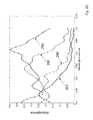
- FIG. 1Cshows exemplary absorption spectra of two nanowires in two subpixels in a pixel of the image sensor of FIG. 1A and a photodiode on the substrate of the image sensor of FIG. 1A .
- FIG. 2Ashows a schematic cross-sectional view of an image sensor according to an embodiment.
- FIG. 2Bshows a schematic top view of the image sensor of FIG. 2A .
- FIG. 2Cshows exemplary absorption spectra of three nanowires in three subpixels in a pixel of the image sensor of FIG. 2A and the substrate of the image sensor of FIG. 2A .
- FIG. 2Dshows exemplary absorption spectra of four nanowires in four subpixels in a pixel of the image sensor of FIG. 2A and the substrate of the image sensor of FIG. 2A .
- FIG. 3shows a schematic of couplers and an infrared filter.
- FIG. 4shows exemplary color-matching functions of three subpixels in the image sensor, and color-matching functions the CIE standard observer.
- the human eyehas photoreceptors (called cone cells) for medium- and high-brightness color vision, with sensitivity peaks in short (S, 420-440 nm), middle (M, 530-540 nm), and long (L, 560-580 nm) wavelengths (there is also the low-brightness monochromatic “night-vision” receptor, called rod cell, with peak sensitivity at 490-495 nm).
- cone cellsfor medium- and high-brightness color vision, with sensitivity peaks in short (S, 420-440 nm), middle (M, 530-540 nm), and long (L, 560-580 nm) wavelengths (there is also the low-brightness monochromatic “night-vision” receptor, called rod cell, with peak sensitivity at 490-495 nm).
- rod cellthe low-brightness monochromatic “night-vision” receptor
- the tristimulus valuesare not the S, M, and L responses of the human eye, but rather a set of tristimulus values called X, Y, and Z, which are roughly red, green and blue, respectively (note that the X, Y, Z values are not physically observed red, green, blue colors. Rather, they may be thought of as ‘derived’ parameters from the red, green, blue colors).
- Two light sources, made up of different mixtures of various wavelengths,may appear to be the same color; this effect is called metamerism. Two light sources have the same apparent color to an observer when they have the same tristimulus values, no matter what spectral distributions of light were used to produce them.
- the tristimulus valuesdepend on the observer's field of view.
- the CIEdefined the standard (colorimetric) observer. Originally this was taken to be the chromatic response of the average human viewing through a 2° angle, due to the belief that the color-sensitive cones resided within a 2° arc of the fovea. Thus the CIE 1931 Standard Observer is also known as the CIE 1931 2° Standard Observer. A more modern but less-used alternative is the CIE 1964 10° Standard Observer, which is derived from the work of Stiles and Burch, and Speranskaya.
- the color matching functionsare the numerical description of the chromatic response of the observer as described above.
- the CIEhas defined a set of three color-matching functions, called, x ( ⁇ ), y ( ⁇ ), and z ( ⁇ ), which can be thought of as the spectral sensitivity curves of three linear light detectors that yield the CIE XYZ tristimulus values X, Y, and Z. These functions are known collectively as the CIE standard observer.
- ⁇is the wavelength of the equivalent monochromatic light (measured in nanometers).
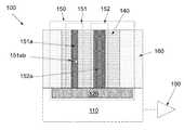
- FIG. 1Ashows a schematic partial cross-sectional view of an image sensor 100 , according to an embodiment.
- the image sensor 100comprises a substrate 110 , one or more pixels 150 .
- At least one pixel 150comprises a clad 140 and a plurality of subpixels embedded in the clad 140 .
- Two subpixels 151 and 152are shown in FIG. 1A as an example.
- Each of the subpixelscomprises a nanowire (e.g. a nanowire 151 a in the subpixel 151 and a nanowire 152 a in the subpixel 152 ) extending essentially perpendicularly from the substrate 110 .
- Space between the pixels 150is preferably filled with a material 160 .
- Each pixel 150can further comprise one or more photodiodes 120 located between the substrate 110 and the nanowires 151 a and 152 a.
- the substrate 110can comprise any suitable material such as silicon, silicon oxide, silicon nitride, sapphire, diamond, silicon carbide, gallium nitride, germanium, indium gallium arsenide, lead sulfide, and/or a combination thereof.
- the photodiode 120can be any suitable photodiode.
- the photodiode 120can have a p-n junction of a p-i-n junction and any suitable circuitry.
- the photodiode 120preferably has a footprint that completely encloses a footprint of the clad 140 .
- the clad 140can comprise any suitable material, such as silicon nitride, silicon oxide, and/or a combination thereof.
- the clad 140is preferably substantially transparent to visible light, preferably with a transmittance of at least 50%, more preferably at least 70%, most preferably at least 90%.
- the clad 140is silicon nitride and has a cylindrical shape with a diameter of about 300 nm.
- the material 160can comprise any suitable material such as silicon dioxide.
- a refractive index of the material 160is preferably smaller than a refractive index of the clad 140 .
- the nanowires (e.g. 151 a and 152 a ) in the subpixels (e.g. 151 and 152 )have refractive indexes equal to or greater than the refractive index of the clad 140 .
- the nanowires and the photodiode 120have different absorption spectra.
- the nanowire 151 ahas strong absorptance in blue wavelengths, as shown by an exemplary absorption spectrum 181 in FIG. 1C ;
- the nanowire 152 ahas a strong absorptance in green wavelengths, as shown by an exemplary absorption spectrum 182 in FIG.
- the photodiode 120has strong absorptance in red wavelengths, as shown by an exemplary absorption spectrum 180 in FIG. 1C .
- the nanowirescan have different diameters and/or different materials. Each nanowire in one pixel 150 preferably has a distance of at least 100 nm, preferable at least 200 nm, to a nearest neighboring nanowire in the same pixel. The nanowires can be positioned at any suitable positions in the clad 140 .
- the nanowires (e.g. 151 a and 152 a ) in the subpixels (e.g. 151 and 152 )are operable to generate electrical signals upon receiving light.
- One exemplary nanowireis a photodiode with a p-n or p-i-n junction therein, details of which can be found in U.S. patent application Ser. Nos. 12/575,221 and 12/633,305, each of which is hereby incorporated by reference in its entirety.
- the electrical signalscan comprise an electrical voltage, an electrical current, an electrical conductance or resistance, and/or a change thereof.
- the nanowirescan have a surface passivation layer.
- Substantially all visible light (e.g. >50%, >70%, or >90%) impinged on the image sensor 100is absorbed by the subpixels (e.g. 151 and 152 ) and the photodiode 120 .
- the subpixels and the photodiodeabsorb light with different wavelengths.
- the image sensor 100can further comprise electronic circuitry 190 operable to detect electrical signals from the subpixels and the photodiode 120 .
- each pixel 150has two subpixels 151 and 152 .
- Each subpixel 151 and 152has only one nanowire 151 a and 152 a , respectively.
- the nanowire 151 acomprises silicon, has a radius of about 25 nm, and has a strong absorptance in blue wavelengths.
- the nanowire 152 acomprises silicon, has a radius of about 40 nm and has a strong absorptance in cyan wavelengths.
- the nanowires 151 a and 152 aare about 200 nm apart but embedded in the same clad 140 .
- Each of the pixels 150can have more than two subpixels according to an embodiment.
- the nanowirescan comprise other suitable materials such as mercury cadmium telluride.
- the nanowirescan have other suitable radii from 10 nm to 250 nm.
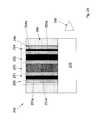
- FIG. 1Bshows a schematic partial top view of the image sensor 100 .
- the pixels 150can have different orientations, which reduces or eliminates effects of directions of incident light.
- the subpixels 151 and 152 and the photodiode 120 in each pixel 150 of the image sensor 100has color matching functions substantially the same as the color matching functions of the CIE 1931 2° Standard Observer or the CIE 1964 10° Standard Observer.
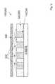
- FIG. 2Ashows a schematic partial cross-sectional view of an image sensor 200 , according to an embodiment.
- the image sensor 200comprises a substrate 210 , one or more pixels 250 .
- the substrate 210preferably does not comprise any photodiode therein.
- At least one pixel 250comprises a clad 240 and a plurality of subpixels embedded in the clad 240 .
- Three subpixels 251 , 252 and 253are shown in FIG. 2A as an example.
- Each of the subpixelscomprises a nanowire (e.g.
- Space between the pixels 250is preferably filled with a material 260 .
- the substrate 210can comprise any suitable material such as silicon, silicon oxide, silicon nitride, sapphire, diamond, silicon carbide, gallium nitride, germanium, indium gallium arsenide, lead sulfide and/or a combination thereof.
- the clad 240can comprise any suitable material, such as silicon nitride, silicon oxide, etc.
- the clad 240is preferably substantially transparent to visible light, preferably with a transmittance of at least 50%, more preferably at least 70%, most preferably at least 90%.
- the clad 240is silicon nitride and has a cylindrical shape with a diameter of about 300 nm.
- the material 260can comprise any suitable material such as silicon dioxide.
- a refractive index of the material 260is preferably smaller than a refractive index of the clad 240 .
- the nanowires (e.g. 251 a , 252 a and 253 a ) in the subpixels (e.g. 251 , 252 and 253 )have refractive indexes equal to or greater than the refractive index of the clad 240 .
- the nanowires and the substrate 210have different absorption spectra.
- the nanowire 251 ahas strong absorptance in blue wavelengths, as shown by an exemplary absorption spectrum 281 in FIG. 2C ;
- the nanowire 252 ahas a strong absorptance in green wavelengths, as shown by an exemplary absorption spectrum 282 in FIG.
- the nanowirescan have different diameters and/or different materials.
- Each nanowire in one pixel 250preferably has a distance of at least 100 nm, preferable at least 200 nm, to a nearest neighboring nanowire in the same pixel.
- the nanowires in the clad 240can be positioned at any suitable positions in the clad 240 .
- the nanowirescan have a surface passivation layer.
- the nanowirescan comprise other suitable materials such as mercury cadmium telluride.
- the nanowirescan have other suitable radii from 10 nm to 250 nm.
- the nanowires (e.g. 251 a , 252 a and 253 a ) in the subpixels (e.g. 251 , 252 and 253 )are operable to generate electrical signals upon receiving light.
- One exemplary nanowireis a photodiode with a p-n or p-i-n junction therein, details of which can be found in U.S. patent application Ser. Nos. 12/575,221 and 12/633,305, each of which is hereby incorporated by reference in its entirety.
- the electrical signalscan comprise an electrical voltage, an electrical current, an electrical conductance or resistance, and/or a change thereof.
- Substantially all visible light impinged on the image sensor 200is absorbed by the subpixels (e.g. 251 , 252 and 253 ).
- the subpixelsabsorb light with different wavelengths.
- the image sensor 200can further comprise electronic circuitry 290 operable to detect electrical signals from the subpixels.
- each pixel 250has three subpixels 251 , 252 and 253 .
- Each subpixel 251 , 252 and 253has only one nanowire 251 a , 252 a and 253 a , respectively.
- the nanowire 251 acomprises silicon, has a radius of about 25 nm, and has a strong absorptance in blue wavelengths.
- the nanowire 252 acomprises silicon, has a radius of about 40 nm and has a strong absorptance in green wavelengths.
- the nanowire 253 acomprises silicon, has a radius of about 45 nm and has a strong absorptance across the entire visible spectrum.
- the nanowires 251 a , 252 a and 253 aare about 200 nm apart but embedded in the same clad 240 .
- the clad 140is cylindrical in shape with a diameter of about 400 nm.
- Each of the pixels 250can have more than three subpixels according to an embodiment.
- each pixel 250has four subpixels 251 , 252 , 253 and 254 .
- Each subpixel 251 , 252 , 253 and 254has only one nanowire 251 a , 252 a , 253 a and 254 a respectively.
- the nanowire 251 acomprises silicon, has a radius of about 25 nm, and has a strong absorptance in blue wavelengths.
- the nanowire 252 acomprises silicon, has a radius of about 40 nm and has a strong absorptance in green wavelengths.
- the nanowire 253 acomprises silicon, has a radius of about 45 nm and has a strong absorptance across the entire visible spectrum.
- the nanowire 254 acomprises silicon, has a radius of about 35 nm and has a strong absorptance in blue green wavelength (e.g. 400 to 550 nm).
- the nanowires 251 a , 252 a , 253 a and 254 aare about 200 nm apart but embedded in the same clad 240 .
- the clad 140is cylindrical in shape with a diameter of about 400 nm.
- FIG. 2Dshows exemplary absorption spectra 291 , 292 , 293 and 294 of the nanowires 251 a , 252 a , 253 a and 254 a , respectively.
- FIG. 2Bshows a schematic partial top view of the image sensor 200 .
- the pixels 250can have different orientations, which reduces or eliminates effects of directions of incident light.
- the image sensor 100 or 200can further comprise couplers 350 above each pixel 150 or 250 , as shown in FIG. 3 .
- Each of the couplers 350preferably has substantially the same footprint as the pixel underneath and has a convex surface.
- the coupler 350is effective to focus substantially all visible light impinged thereon into the clad 140 or 240 .
- the image sensor 100 or 200can further comprise an infrared filter 360 , which is operable to prevent infrared light, such as light with wavelengths above 650 nm, from reaching the pixels.
- the image sensor 100 or 200does not comprise an infrared filter.
- the nanowirescan be made by a dry etching process or a Vapor Liquid Solid (VLS) growth method.
- VLSVapor Liquid Solid
- other materials and/or fabrication techniquesmay also be used for fabricating the nanowires in keeping with the scope of the invention.
- nanowires fabricated from an indium arsenide (InAs) wafer or related materialscould be used for IR applications.
- each nanowirecan also be made to have a strong absorption in wavelengths not in the visible spectrum, such as in the ultraviolet (UV) or infrared (IR) spectra.
- each nanowirecan have transistor (e.g., transistor 151 ab in FIG. 1A ) therein or thereon.
- the subpixels 251 , 252 and 253 in each pixel 250 of the image sensor 200has color matching functions substantially the same as the color matching functions of the CIE 1931 2° Standard Observer or the CIE 1964 10° Standard Observer.
- FIG. 4shows exemplary color-matching functions 451 , 452 and 453 of the subpixels 251 , 252 and 253 , respectively.
- the color-matching functions 461 , 462 and 463are the x ( ⁇ ), y ( ⁇ ), and z ( ⁇ ) of the CIE standard observer.
- the image sensor 100 or 200can be used to sense and capture images.
- a method of sensing an imagecomprises projecting the image onto the image sensor 100 or 200 using any suitable optics such as lenses and/or mirrors; detecting an electrical signal from the nanowire in each subpixel in each pixel using suitable circuitry; calculating a color of each pixel from the electrical signals of the subpixels therein.
Landscapes
- Chemical & Material Sciences (AREA)
- Engineering & Computer Science (AREA)
- Nanotechnology (AREA)
- Crystallography & Structural Chemistry (AREA)
- Physics & Mathematics (AREA)
- Materials Engineering (AREA)
- Optics & Photonics (AREA)
- Biophysics (AREA)
- Composite Materials (AREA)
- Condensed Matter Physics & Semiconductors (AREA)
- General Physics & Mathematics (AREA)
- Life Sciences & Earth Sciences (AREA)
- Solid State Image Pick-Up Elements (AREA)
- Light Receiving Elements (AREA)
- Transforming Light Signals Into Electric Signals (AREA)
Abstract
Description
wherein λ is the wavelength of the equivalent monochromatic light (measured in nanometers).
Claims (38)
Priority Applications (24)
| Application Number | Priority Date | Filing Date | Title |
|---|---|---|---|
| US12/945,492US9515218B2 (en) | 2008-09-04 | 2010-11-12 | Vertical pillar structured photovoltaic devices with mirrors and optical claddings |
| US12/967,880US8748799B2 (en) | 2010-12-14 | 2010-12-14 | Full color single pixel including doublet or quadruplet si nanowires for image sensors |
| US13/106,851US9082673B2 (en) | 2009-10-05 | 2011-05-12 | Passivated upstanding nanostructures and methods of making the same |
| CN201180065814.8ACN103339744B (en) | 2010-12-14 | 2011-12-13 | The single pixel of full color that is double or quadruple silicon nanowires is comprised for imageing sensor |
| KR1020137018243AKR101422144B1 (en) | 2010-12-14 | 2011-12-13 | Full color single pixel including doublet or quadruplet si nanowires for image sensors |
| JP2013544690AJP5540161B2 (en) | 2010-12-14 | 2011-12-13 | Full color single pixel with double or quadruple silicon nanowires for image sensors |
| PCT/US2011/064635WO2012082734A1 (en) | 2010-12-14 | 2011-12-13 | Full color single pixel including doublet or quadruplet si nanowires for image sensors |
| TW103145582ATW201513325A (en) | 2010-12-14 | 2011-12-14 | Full color single pixel with dual or quadruple nanowire for image sensors |
| TW100146327ATWI472020B (en) | 2010-12-14 | 2011-12-14 | Full color single pixel with dual or quadruple nanowire for image sensors |
| US13/925,429US9304035B2 (en) | 2008-09-04 | 2013-06-24 | Vertical waveguides with various functionality on integrated circuits |
| JP2014094365AJP2014209625A (en) | 2010-12-14 | 2014-05-01 | Fully colored single pixel equipped with two or four sets of silicon nano wires for image sensor |
| US14/291,888US9543458B2 (en) | 2010-12-14 | 2014-05-30 | Full color single pixel including doublet or quadruplet Si nanowires for image sensors |
| US14/503,598US9410843B2 (en) | 2008-09-04 | 2014-10-01 | Nanowire arrays comprising fluorescent nanowires and substrate |
| US14/516,402US20160111460A1 (en) | 2008-09-04 | 2014-10-16 | Back-lit photodetector |
| US14/516,162US20160111562A1 (en) | 2008-09-04 | 2014-10-16 | Multispectral and polarization-selective detector |
| US14/632,739US9601529B2 (en) | 2008-09-04 | 2015-02-26 | Light absorption and filtering properties of vertically oriented semiconductor nano wires |
| US14/704,143US20150303333A1 (en) | 2008-09-04 | 2015-05-05 | Passivated upstanding nanostructures and methods of making the same |
| US14/705,380US9337220B2 (en) | 2008-09-04 | 2015-05-06 | Solar blind ultra violet (UV) detector and fabrication methods of the same |
| US15/057,153US20160178840A1 (en) | 2008-09-04 | 2016-03-01 | Optical waveguides in image sensors |
| US15/082,514US20160211394A1 (en) | 2008-11-13 | 2016-03-28 | Nano wire array based solar energy harvesting device |
| US15/090,155US20160216523A1 (en) | 2008-09-04 | 2016-04-04 | Vertical waveguides with various functionality on integrated circuits |
| US15/093,928US20160225811A1 (en) | 2008-09-04 | 2016-04-08 | Nanowire structured color filter arrays and fabrication method of the same |
| US15/149,252US20160254301A1 (en) | 2008-09-04 | 2016-05-09 | Solar blind ultra violet (uv) detector and fabrication methods of the same |
| US15/225,264US20160344964A1 (en) | 2008-09-04 | 2016-08-01 | Methods for fabricating and using nanowires |
Applications Claiming Priority (1)
| Application Number | Priority Date | Filing Date | Title |
|---|---|---|---|
| US12/967,880US8748799B2 (en) | 2010-12-14 | 2010-12-14 | Full color single pixel including doublet or quadruplet si nanowires for image sensors |
Related Parent Applications (2)
| Application Number | Title | Priority Date | Filing Date |
|---|---|---|---|
| US12/966,573Continuation-In-PartUS8866065B2 (en) | 2008-09-04 | 2010-12-13 | Nanowire arrays comprising fluorescent nanowires |
| US12/974,499Continuation-In-PartUS8507840B2 (en) | 2008-09-04 | 2010-12-21 | Vertically structured passive pixel arrays and methods for fabricating the same |
Related Child Applications (3)
| Application Number | Title | Priority Date | Filing Date |
|---|---|---|---|
| US12/966,573Continuation-In-PartUS8866065B2 (en) | 2008-09-04 | 2010-12-13 | Nanowire arrays comprising fluorescent nanowires |
| US12/974,499Continuation-In-PartUS8507840B2 (en) | 2008-09-04 | 2010-12-21 | Vertically structured passive pixel arrays and methods for fabricating the same |
| US14/291,888ContinuationUS9543458B2 (en) | 2008-09-04 | 2014-05-30 | Full color single pixel including doublet or quadruplet Si nanowires for image sensors |
Publications (2)
| Publication Number | Publication Date |
|---|---|
| US20120145880A1 US20120145880A1 (en) | 2012-06-14 |
| US8748799B2true US8748799B2 (en) | 2014-06-10 |
Family
ID=46198365
Family Applications (2)
| Application Number | Title | Priority Date | Filing Date |
|---|---|---|---|
| US12/967,880Expired - Fee RelatedUS8748799B2 (en) | 2008-09-04 | 2010-12-14 | Full color single pixel including doublet or quadruplet si nanowires for image sensors |
| US14/291,888Expired - Fee RelatedUS9543458B2 (en) | 2008-09-04 | 2014-05-30 | Full color single pixel including doublet or quadruplet Si nanowires for image sensors |
Family Applications After (1)
| Application Number | Title | Priority Date | Filing Date |
|---|---|---|---|
| US14/291,888Expired - Fee RelatedUS9543458B2 (en) | 2008-09-04 | 2014-05-30 | Full color single pixel including doublet or quadruplet Si nanowires for image sensors |
Country Status (6)
| Country | Link |
|---|---|
| US (2) | US8748799B2 (en) |
| JP (2) | JP5540161B2 (en) |
| KR (1) | KR101422144B1 (en) |
| CN (1) | CN103339744B (en) |
| TW (2) | TWI472020B (en) |
| WO (1) | WO2012082734A1 (en) |
Cited By (15)
| Publication number | Priority date | Publication date | Assignee | Title |
|---|---|---|---|---|
| US20140263967A1 (en)* | 2010-12-14 | 2014-09-18 | Zena Technologies, Inc. | Full color single pixel including doublet or quadruplet si nanowires for image sensors |
| US20150009373A1 (en)* | 2012-03-28 | 2015-01-08 | Fujifilm Corporation | Imaging element and imaging apparatus |
| US9299866B2 (en) | 2010-12-30 | 2016-03-29 | Zena Technologies, Inc. | Nanowire array based solar energy harvesting device |
| US9304035B2 (en) | 2008-09-04 | 2016-04-05 | Zena Technologies, Inc. | Vertical waveguides with various functionality on integrated circuits |
| US9337220B2 (en) | 2008-09-04 | 2016-05-10 | Zena Technologies, Inc. | Solar blind ultra violet (UV) detector and fabrication methods of the same |
| US9343490B2 (en) | 2013-08-09 | 2016-05-17 | Zena Technologies, Inc. | Nanowire structured color filter arrays and fabrication method of the same |
| US9406709B2 (en) | 2010-06-22 | 2016-08-02 | President And Fellows Of Harvard College | Methods for fabricating and using nanowires |
| US9410843B2 (en) | 2008-09-04 | 2016-08-09 | Zena Technologies, Inc. | Nanowire arrays comprising fluorescent nanowires and substrate |
| US9425341B2 (en) | 2012-10-08 | 2016-08-23 | Agency For Science, Technology And Research | P-I-N photodiode with dopant diffusion barrier layer |
| US9478685B2 (en) | 2014-06-23 | 2016-10-25 | Zena Technologies, Inc. | Vertical pillar structured infrared detector and fabrication method for the same |
| US9490283B2 (en) | 2009-11-19 | 2016-11-08 | Zena Technologies, Inc. | Active pixel sensor with nanowire structured photodetectors |
| US9515218B2 (en) | 2008-09-04 | 2016-12-06 | Zena Technologies, Inc. | Vertical pillar structured photovoltaic devices with mirrors and optical claddings |
| US20210345469A1 (en)* | 2019-01-18 | 2021-11-04 | Opple Lighting Co., Ltd. | Measurement method and device of light source parameters, illumination system and terminal apparatus |
| US20220013917A1 (en)* | 2012-09-16 | 2022-01-13 | Shalom Wertsberger | Continuous resonance trap refractor based assembly |
| US12149850B2 (en) | 2021-09-15 | 2024-11-19 | Samsung Electronics Co., Ltd. | Image sensor and electronic apparatus including the image sensor |
Families Citing this family (12)
| Publication number | Priority date | Publication date | Assignee | Title |
|---|---|---|---|---|
| US9800805B2 (en)* | 2011-02-02 | 2017-10-24 | The Boeing Company | Frequency selective imaging system |
| WO2014022828A1 (en)* | 2012-08-02 | 2014-02-06 | The Regents Of The University Of California | Integrated nanowire array devices for detecting and/or applying electrical signals to tissue |
| WO2014028380A2 (en)* | 2012-08-13 | 2014-02-20 | President And Fellows Of Harvard College | Multispectral imaging using silicon nanowires |
| FR3008546B1 (en)* | 2013-07-12 | 2015-08-07 | Commissariat Energie Atomique | SEMI-TRANSPARENT PHOTODETECTOR WITH STRUCTURED P-N JUNCTION |
| JP2015065270A (en)* | 2013-09-25 | 2015-04-09 | ソニー株式会社 | Solid state image pickup device and manufacturing method of the same, and electronic apparatus |
| EP3084346A4 (en)* | 2013-12-19 | 2017-08-23 | 3M Innovative Properties Company | Object sensor |
| EP3099081B1 (en) | 2015-05-28 | 2020-04-29 | Samsung Electronics Co., Ltd. | Display apparatus and control method thereof |
| US10431624B2 (en) | 2015-07-08 | 2019-10-01 | Samsung Electronics Co., Ltd. | Method of manufacturing image sensor including nanostructure color filter |
| KR101834049B1 (en)* | 2015-12-29 | 2018-04-13 | 전자부품연구원 | Image sensor using a nanowire and method of manufacturing the same |
| CN110047861B (en)* | 2019-04-30 | 2021-05-07 | 德淮半导体有限公司 | Image sensor, forming method and operating method thereof |
| CN110061022B (en)* | 2019-04-30 | 2021-04-13 | 德淮半导体有限公司 | Image sensor and method of forming the same |
| JPWO2021044831A1 (en) | 2019-09-02 | 2021-03-11 |
Citations (379)
| Publication number | Priority date | Publication date | Assignee | Title |
|---|---|---|---|---|
| US1918848A (en) | 1929-04-26 | 1933-07-18 | Norwich Res Inc | Polarizing refracting bodies |
| US3903427A (en) | 1973-12-28 | 1975-09-02 | Hughes Aircraft Co | Solar cell connections |
| US4017332A (en) | 1975-02-27 | 1977-04-12 | Varian Associates | Solar cells employing stacked opposite conductivity layers |
| US4357415A (en) | 1980-03-06 | 1982-11-02 | Eastman Kodak Company | Method of making a solid-state color imaging device having a color filter array using a photocrosslinkable barrier |
| US4387265A (en) | 1981-07-17 | 1983-06-07 | University Of Delaware | Tandem junction amorphous semiconductor photovoltaic cell |
| US4400221A (en) | 1981-07-08 | 1983-08-23 | The United States Of America As Represented By The Secretary Of The Air Force | Fabrication of gallium arsenide-germanium heteroface junction device |
| US4443890A (en) | 1980-12-02 | 1984-04-17 | Thomson-Csf | Optical-connection direct-light modulation information transmission system with a passband extended towards the low frequencies and continuous waves |
| US4513168A (en) | 1984-04-19 | 1985-04-23 | Varian Associates, Inc. | Three-terminal solar cell circuit |
| US4620237A (en) | 1984-10-22 | 1986-10-28 | Xerox Corporation | Fast scan jitter measuring system for raster scanners |
| US4678772A (en) | 1983-02-28 | 1987-07-07 | Yissum Research Development Company Of The Hebrew University Of Jerusalem | Compositions containing glycyrrhizin |
| US4827335A (en) | 1986-08-29 | 1989-05-02 | Kabushiki Kaisha Toshiba | Color image reading apparatus with two color separation filters each having two filter elements |
| US4846556A (en) | 1987-05-14 | 1989-07-11 | Toppan Printing Co., Ltd. | Color filter and method of manufacturing the same |
| US4880613A (en) | 1987-01-12 | 1989-11-14 | Sumitomo Electric Industries, Ltd. | Light emitting element comprising diamond and method for producing the same |
| US4896941A (en) | 1985-04-27 | 1990-01-30 | Doryokuro Kakunenryo Kaihatsu Jigyodan | Image-transmitting fiber |
| US4950625A (en) | 1988-06-13 | 1990-08-21 | Sumitomo Electric Industries, Ltd. | Diamond laser crystal and method manufacturing the same |
| US4972244A (en) | 1988-06-16 | 1990-11-20 | Commissariat A L'energie Atomique | Photodiode and photodiode array on a II-VI material and processes for the production thereof |
| US4971928A (en) | 1990-01-16 | 1990-11-20 | General Motors Corporation | Method of making a light emitting semiconductor having a rear reflecting surface |
| US5096520A (en) | 1990-08-01 | 1992-03-17 | Faris Sades M | Method for producing high efficiency polarizing filters |
| US5124543A (en) | 1989-08-09 | 1992-06-23 | Ricoh Company, Ltd. | Light emitting element, image sensor and light receiving element with linearly varying waveguide index |
| US5247349A (en) | 1982-11-16 | 1993-09-21 | Stauffer Chemical Company | Passivation and insulation of III-V devices with pnictides, particularly amorphous pnictides having a layer-like structure |
| US5272518A (en) | 1990-12-17 | 1993-12-21 | Hewlett-Packard Company | Colorimeter and calibration system |
| US5311047A (en) | 1988-11-16 | 1994-05-10 | National Science Council | Amorphous SI/SIC heterojunction color-sensitive phototransistor |
| US5347147A (en) | 1990-11-28 | 1994-09-13 | Jones Barbara L | Light emitting diamond device |
| US5362972A (en) | 1990-04-20 | 1994-11-08 | Hitachi, Ltd. | Semiconductor device using whiskers |
| US5374841A (en) | 1991-12-18 | 1994-12-20 | Texas Instruments Incorporated | HgCdTe S-I-S two color infrared detector |
| US5401968A (en) | 1989-12-29 | 1995-03-28 | Honeywell Inc. | Binary optical microlens detector array |
| US5449626A (en) | 1991-12-27 | 1995-09-12 | Hezel; Rudolf | Method for manufacture of a solar cell |
| US5468652A (en) | 1993-07-14 | 1995-11-21 | Sandia Corporation | Method of making a back contacted solar cell |
| US5602661A (en) | 1993-02-17 | 1997-02-11 | Hoffmann-La Roche Inc. | Optical component |
| US5612780A (en) | 1996-06-05 | 1997-03-18 | Harris Corporation | Device for detecting light emission from optical fiber |
| US5671914A (en) | 1995-11-06 | 1997-09-30 | Spire Corporation | Multi-band spectroscopic photodetector array |
| US5696863A (en) | 1982-08-06 | 1997-12-09 | Kleinerman; Marcos Y. | Distributed fiber optic temperature sensors and systems |
| US5723945A (en) | 1996-04-09 | 1998-03-03 | Electro Plasma, Inc. | Flat-panel display |
| US5747796A (en) | 1995-07-13 | 1998-05-05 | Sharp Kabushiki Kaisha | Waveguide type compact optical scanner and manufacturing method thereof |
| US5767507A (en) | 1996-07-15 | 1998-06-16 | Trustees Of Boston University | Polarization sensitive photodetectors and detector arrays |
| US5798535A (en) | 1996-12-20 | 1998-08-25 | Motorola, Inc. | Monolithic integration of complementary transistors and an LED array |
| US5844290A (en) | 1996-06-27 | 1998-12-01 | Nec Corporation | Solid state image pick-up device and method for manufacturing the same |
| US5853446A (en) | 1996-04-16 | 1998-12-29 | Corning Incorporated | Method for forming glass rib structures |
| US5857053A (en) | 1997-06-17 | 1999-01-05 | Lucent Technologies Inc. | Optical fiber filter |
| US5877492A (en) | 1995-09-14 | 1999-03-02 | Nec Corporation | Contact type image sensor comprising a plurality of microlenses |
| US5880495A (en) | 1998-01-08 | 1999-03-09 | Omnivision Technologies, Inc. | Active pixel with a pinned photodiode |
| US5885881A (en) | 1996-04-24 | 1999-03-23 | Northern Telecom Limited | Planar wave guide cladding |
| US5900623A (en) | 1997-08-11 | 1999-05-04 | Chrontel, Inc. | Active pixel sensor using CMOS technology with reverse biased photodiodes |
| US5943463A (en) | 1996-06-17 | 1999-08-24 | Sharp Kabushiki Kaisha | Color image sensor and a production method of an optical waveguide array for use therein |
| US5968528A (en) | 1997-05-23 | 1999-10-19 | The Procter & Gamble Company | Skin care compositions |
| US6033582A (en) | 1996-01-22 | 2000-03-07 | Etex Corporation | Surface modification of medical implants |
| US6037243A (en) | 1997-11-06 | 2000-03-14 | Electronics And Telecommunications Research Institute | Method for manufacturing silicon nanometer structure using silicon nitride film |
| US6046466A (en) | 1997-09-12 | 2000-04-04 | Nikon Corporation | Solid-state imaging device |
| US6074892A (en) | 1996-05-07 | 2000-06-13 | Ciena Corporation | Semiconductor hetero-interface photodetector |
| US6100551A (en) | 1995-04-13 | 2000-08-08 | Eastman Kodak Company | Active pixel sensor integrated with a pinned photodiode |
| GB2348399A (en) | 1999-03-31 | 2000-10-04 | Univ Glasgow | Reactive ion etching with control of etch gas flow rate, pressure and rf power |
| US6270548B1 (en) | 1997-04-17 | 2001-08-07 | James Wilbert Campbell | Sintering process for diamond and diamond growth |
| US6301420B1 (en) | 1998-05-01 | 2001-10-09 | The Secretary Of State For Defence In Her Britannic Majesty's Government Of The United Kingdom Of Great Britain And Northern Ireland | Multicore optical fibre |
| US6326649B1 (en) | 1999-01-13 | 2001-12-04 | Agere Systems, Inc. | Pin photodiode having a wide bandwidth |
| US20020003201A1 (en) | 1998-02-02 | 2002-01-10 | Gang Yu | Image sensors made from organic semiconductors |
| US20020020846A1 (en) | 2000-04-20 | 2002-02-21 | Bo Pi | Backside illuminated photodiode array |
| US20020021879A1 (en) | 2000-07-10 | 2002-02-21 | Lee Kevin K. | Graded index waveguide |
| US6388648B1 (en) | 1996-11-05 | 2002-05-14 | Clarity Visual Systems, Inc. | Color gamut and luminance matching techniques for image display systems |
| US6388243B1 (en) | 1999-03-01 | 2002-05-14 | Photobit Corporation | Active pixel sensor with fully-depleted buried photoreceptor |
| JP2002151715A (en) | 2000-11-08 | 2002-05-24 | Sharp Corp | Thin film solar cell |
| US6407439B1 (en) | 1999-08-19 | 2002-06-18 | Epitaxial Technologies, Llc | Programmable multi-wavelength detector array |
| US20020104821A1 (en) | 1996-10-04 | 2002-08-08 | Michael Bazylenko | Reactive ion etching of silica structures |
| US20020109082A1 (en) | 2001-02-13 | 2002-08-15 | Yoshikazu Nakayama And Daiken Chemical Co., Ltd. | Light receiving and emitting probe and light receiving and emitting probe apparatus |
| US20020130311A1 (en) | 2000-08-22 | 2002-09-19 | Lieber Charles M. | Doped elongated semiconductors, growing such semiconductors, devices including such semiconductors and fabricating such devices |
| US6459034B2 (en) | 2000-06-01 | 2002-10-01 | Sharp Kabushiki Kaisha | Multi-junction solar cell |
| US6463204B1 (en) | 1998-12-18 | 2002-10-08 | Fujitsu Network Communications, Inc. | Modular lightpipe system |
| US20020172820A1 (en) | 2001-03-30 | 2002-11-21 | The Regents Of The University Of California | Methods of fabricating nanostructures and nanowires and devices fabricated therefrom |
| US20030003300A1 (en) | 2001-07-02 | 2003-01-02 | Korgel Brian A. | Light-emitting nanoparticles and method of making same |
| US20030006363A1 (en) | 2001-04-27 | 2003-01-09 | Campbell Scott Patrick | Optimization of alignment between elements in an image sensor |
| US6542231B1 (en) | 2000-08-22 | 2003-04-01 | Thermo Finnegan Llc | Fiber-coupled liquid sample analyzer with liquid flow cell |
| US20030077907A1 (en) | 1999-08-06 | 2003-04-24 | Kao David Y. | Method for forming an etch mask during the manufacture of a semiconductor device |
| US6563995B2 (en) | 2001-04-02 | 2003-05-13 | Lightwave Electronics | Optical wavelength filtering apparatus with depressed-index claddings |
| US20030089899A1 (en) | 2000-08-22 | 2003-05-15 | Lieber Charles M. | Nanoscale wires and related devices |
| US6566723B1 (en) | 2002-01-10 | 2003-05-20 | Agilent Technologies, Inc. | Digital color image sensor with elevated two-color photo-detector and related circuitry |
| US20030103744A1 (en) | 2001-02-28 | 2003-06-05 | Yoshimi Koyama | Image input device |
| US20030132480A1 (en) | 2002-01-16 | 2003-07-17 | Duc Chau | Self-aligned trench mosfets and methods for making the same |
| US20030189202A1 (en) | 2002-04-05 | 2003-10-09 | Jun Li | Nanowire devices and methods of fabrication |
| US20030227090A1 (en) | 2002-05-31 | 2003-12-11 | Ichiro Okabe | Dual damascene semiconductor devices |
| US6680216B2 (en) | 2000-03-09 | 2004-01-20 | General Electric Company | Method of making imager structure |
| US20040026684A1 (en) | 2002-04-02 | 2004-02-12 | Nanosys, Inc. | Nanowire heterostructures for encoding information |
| US6709929B2 (en) | 2001-06-25 | 2004-03-23 | North Carolina State University | Methods of forming nano-scale electronic and optoelectronic devices using non-photolithographically defined nano-channel templates |
| US20040058058A1 (en) | 2000-04-12 | 2004-03-25 | Shchegolikhin Alexander Nikitovich | Raman-active taggants and thier recognition |
| US20040065362A1 (en) | 2001-01-31 | 2004-04-08 | Takenori Watabe | Solar cell and method for producing the same |
| US6720594B2 (en) | 2002-01-07 | 2004-04-13 | Xerox Corporation | Image sensor array with reduced pixel crosstalk |
| US20040075464A1 (en) | 2002-07-08 | 2004-04-22 | Btg International Limited | Nanostructures and methods for manufacturing the same |
| US20040095658A1 (en) | 2002-09-05 | 2004-05-20 | Nanosys, Inc. | Nanocomposites |
| US20040109666A1 (en) | 2002-12-10 | 2004-06-10 | John Kim | Optoelectronic devices employing fibers for light collection and emission |
| US20040118377A1 (en) | 2002-12-19 | 2004-06-24 | Bloms Jason K. | Fuel allocation at idle or light engine load |
| US20040118337A1 (en) | 2002-09-30 | 2004-06-24 | Canon Kabushiki Kaisha | Method for growing silicon film, method for manufacturing solar cell, semiconductor substrate, and solar cell |
| US20040122328A1 (en) | 2000-06-19 | 2004-06-24 | University Of Washington | Integrated optical scanning image acquisition and display |
| US20040124366A1 (en) | 2002-10-02 | 2004-07-01 | Haishan Zeng | Apparatus and methods relating to high speed spectroscopy and excitation-emission matrices |
| US6771314B1 (en) | 1998-03-31 | 2004-08-03 | Intel Corporation | Orange-green-blue (OGB) color system for digital image sensor applications |
| US20040156610A1 (en) | 1997-05-16 | 2004-08-12 | Btg International Limited | Optical devices and methods of fabrication thereof |
| US20040155247A1 (en) | 2000-12-21 | 2004-08-12 | Stephan Benthien | Image sensor device comprising central locking |
| US20040180461A1 (en) | 2003-03-12 | 2004-09-16 | Taiwan Semiconductor Manufacturing Company | Light guide for image sensor |
| US6805139B1 (en) | 1999-10-20 | 2004-10-19 | Mattson Technology, Inc. | Systems and methods for photoresist strip and residue treatment in integrated circuit manufacturing |
| US20040213307A1 (en) | 2002-07-19 | 2004-10-28 | President And Fellows Of Harvard College | Nanoscale coherent optical components |
| US6812473B1 (en) | 1999-06-30 | 2004-11-02 | Hoya Corporation | Electron beam drawing mask blank, electron beam drawing mask, and method of manufacturing the same |
| US20040217086A1 (en) | 2002-09-11 | 2004-11-04 | Matsushita Electric Industrial Co., Ltd. | Pattern formation method |
| US20040223681A1 (en) | 2003-04-23 | 2004-11-11 | Block Bruce A. | On-chip optical signal routing |
| US20040241965A1 (en) | 2003-05-28 | 2004-12-02 | Charles Merritt | High aspect ratio microelectrode arrays |
| US20040261840A1 (en) | 2003-06-30 | 2004-12-30 | Advent Solar, Inc. | Emitter wrap-through back contact solar cells on thin silicon wafers |
| US20050009224A1 (en) | 2003-06-20 | 2005-01-13 | The Regents Of The University Of California | Nanowire array and nanowire solar cells and methods for forming the same |
| US20050082676A1 (en) | 2003-10-17 | 2005-04-21 | International Business Machines Corporation | Silicon chip carrier with through-vias using laser assisted chemical vapor deposition of conductor |
| US20050087601A1 (en) | 2003-10-24 | 2005-04-28 | Gerst Carl W.Iii | Light pipe illumination system and method |
| US20050095699A1 (en) | 2002-10-30 | 2005-05-05 | Akihiro Miyauchi | Functioning substrate with a group of columnar micro pillars and its manufacturing method |
| US20050116271A1 (en) | 2003-12-02 | 2005-06-02 | Yoshiaki Kato | Solid-state imaging device and manufacturing method thereof |
| US20050133476A1 (en) | 2003-12-17 | 2005-06-23 | Islam M. S. | Methods of bridging lateral nanowires and device using same |
| WO2005064337A1 (en) | 2003-12-22 | 2005-07-14 | Koninklijke Philips Electronics N.V. | Optical nanowire biosensor based on energy transfer |
| US20050164514A1 (en) | 2004-01-28 | 2005-07-28 | Shahid Rauf | Method for etching a quartz layer in a photoresistless semiconductor mask |
| US6927145B1 (en) | 2004-02-02 | 2005-08-09 | Advanced Micro Devices, Inc. | Bitline hard mask spacer flow for memory cell scaling |
| US20050190453A1 (en) | 2004-03-01 | 2005-09-01 | Hideki Dobashi | Image sensor |
| US20050201704A1 (en) | 2004-02-12 | 2005-09-15 | Panorama Flat Ltd. | Apparatus, method, and computer program product for transverse waveguided display system |
| JP2005252210A (en) | 2004-02-03 | 2005-09-15 | Sharp Corp | Solar cell |
| US20050218468A1 (en) | 2004-03-18 | 2005-10-06 | Owen Mark D | Micro-reflectors on a substrate for high-density LED array |
| US6960526B1 (en) | 2003-10-10 | 2005-11-01 | The United States Of America As Represented By The Secretary Of The Army | Method of fabricating sub-100 nanometer field emitter tips comprising group III-nitride semiconductors |
| US20050242409A1 (en) | 2004-04-28 | 2005-11-03 | Advanced Chip Engineering Technology Inc. | Imagine sensor with a protection layer |
| US6967120B2 (en) | 2002-07-19 | 2005-11-22 | Dongbu Anam Semiconductor | Pinned photodiode for a CMOS image sensor and fabricating method thereof |
| US6969899B2 (en) | 2003-12-08 | 2005-11-29 | Taiwan Semiconductor Manufacturing Co., Ltd. | Image sensor with light guides |
| US20050284517A1 (en) | 2004-06-29 | 2005-12-29 | Sanyo Electric Co., Ltd. | Photovoltaic cell, photovoltaic cell module, method of fabricating photovoltaic cell and method of repairing photovoltaic cell |
| US6987258B2 (en) | 2001-12-19 | 2006-01-17 | Intel Corporation | Integrated circuit-based compound eye image sensor using a light pipe bundle |
| US20060011362A1 (en) | 2002-01-14 | 2006-01-19 | China Petroleum & Chemical Corporation | Power transmission unit of an impactor, a hydraulic jet impactor and the application thereof |
| US20060038990A1 (en) | 2004-08-20 | 2006-02-23 | Habib Youssef M | Nanowire optical sensor system and methods for making and using same |
| US7052927B1 (en) | 2004-01-27 | 2006-05-30 | Raytheon Company | Pin detector apparatus and method of fabrication |
| US20060113622A1 (en) | 2004-11-30 | 2006-06-01 | International Business Machines Corporation | A damascene copper wiring image sensor |
| US20060121371A1 (en) | 2004-12-03 | 2006-06-08 | Innolux Display Corp. | Color filter having nanoparticles for liquid crystal display |
| US7064372B2 (en) | 2002-09-30 | 2006-06-20 | Nanosys, Inc. | Large-area nanoenabled macroelectronic substrates and uses therefor |
| US20060146323A1 (en) | 2005-01-06 | 2006-07-06 | Alexandre Bratkovski | Nanowires for surface-enhanced raman scattering molecular sensors |
| US20060162766A1 (en) | 2003-06-26 | 2006-07-27 | Advent Solar, Inc. | Back-contacted solar cells with integral conductive vias and method of making |
| EP0809303B1 (en) | 1996-05-22 | 2006-09-06 | Eastman Kodak Company | A color active pixel sensor with electronic shuttering, anti-blooming and low cross-talk |
| US7105428B2 (en) | 2004-04-30 | 2006-09-12 | Nanosys, Inc. | Systems and methods for nanowire growth and harvesting |
| US7109517B2 (en) | 2001-11-16 | 2006-09-19 | Zaidi Saleem H | Method of making an enhanced optical absorption and radiation tolerance in thin-film solar cells and photodetectors |
| US20060260674A1 (en) | 2004-04-06 | 2006-11-23 | Tran Bao Q | Nano ic |
| US20060273389A1 (en) | 2005-05-23 | 2006-12-07 | International Business Machines Corporation | Vertical FET with nanowire channels and a silicided bottom contact |
| US20060273262A1 (en) | 2000-12-20 | 2006-12-07 | Michel Sayag | Light stimulating and collecting methods and apparatus for storage-phosphor image plates |
| US20060284118A1 (en) | 2005-06-15 | 2006-12-21 | Board Of Trustees Of Michigan State University | Process and apparatus for modifying a surface in a work region |
| US7153720B2 (en) | 2002-12-09 | 2006-12-26 | Quantum Semiconductor Llc | CMOS image sensor |
| US7163659B2 (en) | 2002-12-03 | 2007-01-16 | Hewlett-Packard Development Company, L.P. | Free-standing nanowire sensor and method for detecting an analyte in a fluid |
| US20070012985A1 (en) | 2004-03-23 | 2007-01-18 | Nanosys, Inc. | Nanowire capacitor and methods of making same |
| US20070012980A1 (en) | 2002-09-30 | 2007-01-18 | Nanosys, Inc. | Large-area nanoenabled macroelectronic substrates and uses therefor |
| US20070025504A1 (en) | 2003-06-20 | 2007-02-01 | Tumer Tumay O | System for molecular imaging |
| US20070023799A1 (en) | 2005-08-01 | 2007-02-01 | Micro Technology, Inc. | Structure and method for building a light tunnel for use with imaging devices |
| US20070029545A1 (en) | 2003-02-24 | 2007-02-08 | Ignis Innovation Inc | Pixel having an organic light emitting diode and method of fabricating the pixel |
| US20070052050A1 (en) | 2005-09-07 | 2007-03-08 | Bart Dierickx | Backside thinned image sensor with integrated lens stack |
| US20070076481A1 (en) | 2005-10-03 | 2007-04-05 | Rockwell Scientific Licensing, Llc | Multimode focal plane array with electrically isolated commons for independent sub-array biasing |
| US20070082255A1 (en) | 2005-10-06 | 2007-04-12 | Gongquan Sun | Fuel cells and fuel cell catalysts incorporating a nanoring support |
| US7208783B2 (en) | 2004-11-09 | 2007-04-24 | Micron Technology, Inc. | Optical enhancement of integrated circuit photodetectors |
| US20070099292A1 (en) | 2001-04-10 | 2007-05-03 | Bioprocessors Corp. | Reactor systems having a light-interacting component |
| US20070104441A1 (en) | 2005-11-08 | 2007-05-10 | Massachusetts Institute Of Technology | Laterally-integrated waveguide photodetector apparatus and related coupling methods |
| US20070108371A1 (en) | 2005-11-16 | 2007-05-17 | Eastman Kodak Company | PMOS pixel structure with low cross talk for active pixel image sensors |
| US20070120254A1 (en) | 2003-12-23 | 2007-05-31 | Koninklijke Philips Electronics N.C. | Semiconductor device comprising a pn-heterojunction |
| US20070126037A1 (en) | 2005-12-06 | 2007-06-07 | Sotomitsu Ikeda | Electric device having nanowires, manufacturing method thereof, and electric device assembly |
| US20070138376A1 (en) | 2005-08-24 | 2007-06-21 | The Trustees Of Boston College | Nanoscale optical microscope |
| US20070139740A1 (en) | 2005-12-20 | 2007-06-21 | Fujitsu Limited | Image processing circuit and image processing method |
| US20070138459A1 (en) | 2005-10-13 | 2007-06-21 | Wong Stanislaus S | Ternary oxide nanostructures and methods of making same |
| US20070137697A1 (en) | 2005-08-24 | 2007-06-21 | The Trustees Of Boston College | Apparatus and methods for solar energy conversion using nanoscale cometal structures |
| US20070140638A1 (en) | 2004-05-13 | 2007-06-21 | The Regents Of The University Of California | Nanowires and nanoribbons as subwavelength optical waveguides and their use as components in photonic circuits and devices |
| US20070138380A1 (en) | 2005-12-16 | 2007-06-21 | Adkisson James W | Funneled light pipe for pixel sensors |
| US7235475B2 (en) | 2004-12-23 | 2007-06-26 | Hewlett-Packard Development Company, L.P. | Semiconductor nanowire fluid sensor and method for fabricating the same |
| US20070148599A1 (en) | 2005-09-13 | 2007-06-28 | Randall True | Multiple step printing methods for microbarcodes |
| US20070145512A1 (en) | 2004-09-27 | 2007-06-28 | Rhodes Howard E | Photogate stack with nitride insulating cap over conductive layer |
| US20070155025A1 (en) | 2006-01-04 | 2007-07-05 | Anping Zhang | Nanowire structures and devices for use in large-area electronics and methods of making the same |
| US20070152248A1 (en) | 2006-01-05 | 2007-07-05 | Korea Advanced Institute Of Science & Technology | Complementary metal oxide semiconductor image sensor and method for fabricating the same |
| US7241434B2 (en) | 2000-08-11 | 2007-07-10 | Bellataire International, Llc | High pressure and high temperature production of diamonds |
| US20070170418A1 (en) | 2005-12-02 | 2007-07-26 | Bowers Michael J | Broad-emission nanocrystals and methods of making and using same |
| US20070172623A1 (en) | 2003-12-18 | 2007-07-26 | Tesa Ag | Optical data store with several storage layers |
| JP2007201091A (en) | 2006-01-25 | 2007-08-09 | Fujifilm Corp | Manufacturing method of solid-state imaging device |
| US20070187787A1 (en) | 2006-02-16 | 2007-08-16 | Ackerson Kristin M | Pixel sensor structure including light pipe and method for fabrication thereof |
| US7262400B2 (en) | 2005-12-02 | 2007-08-28 | Taiwan Semiconductor Manufacturing Co., Ltd. | Image sensor device having an active layer overlying a substrate and an isolating region in the active layer |
| US20070200054A1 (en) | 2006-02-24 | 2007-08-30 | Tower Semiconductor Ltd. | Via wave guide with curved light concentrator for image sensing devices |
| US7265328B2 (en) | 2005-08-22 | 2007-09-04 | Micron Technology, Inc. | Method and apparatus providing an optical guide for an imager pixel having a ring of air-filled spaced slots around a photosensor |
| US20070205483A1 (en) | 2006-01-27 | 2007-09-06 | Williams R S | Mixed-scale electronic interface |
| US7272287B2 (en) | 2005-05-11 | 2007-09-18 | Fitel Usa Corp | Optical fiber filter for suppression of amplified spontaneous emission |
| US20070217754A1 (en) | 2005-10-07 | 2007-09-20 | Takashi Sasaki | Optical fiber, optical transmission line, optical module and optical transmission system |
| US20070228421A1 (en) | 2005-12-06 | 2007-10-04 | Shunsuke Shioya | Semiconductor device using semiconductor nanowire and display apparatus and image pick-up apparatus using the same |
| US20070238265A1 (en) | 2005-04-05 | 2007-10-11 | Keiichi Kurashina | Plating apparatus and plating method |
| US20070238285A1 (en) | 2006-03-31 | 2007-10-11 | Applied Materials, Inc. | Method for making an improved thin film solar cell interconnect using etch and deposition process |
| US20070241260A1 (en) | 2004-09-30 | 2007-10-18 | Osram Opto Semiconductors Gmbh | Radiation detector with an epitaxially grown semiconductor body |
| US7285812B2 (en) | 2004-09-02 | 2007-10-23 | Micron Technology, Inc. | Vertical transistors |
| US20070246689A1 (en) | 2006-04-11 | 2007-10-25 | Jiaxin Ge | Transparent thin polythiophene films having improved conduction through use of nanomaterials |
| US20070248958A1 (en) | 2004-09-15 | 2007-10-25 | Microchip Biotechnologies, Inc. | Microfluidic devices |
| US20070272828A1 (en) | 2006-05-24 | 2007-11-29 | Micron Technology, Inc. | Method and apparatus providing dark current reduction in an active pixel sensor |
| US7306963B2 (en) | 2004-11-30 | 2007-12-11 | Spire Corporation | Precision synthesis of quantum dot nanostructures for fluorescent and optoelectronic devices |
| US7307327B2 (en) | 2005-08-04 | 2007-12-11 | Micron Technology, Inc. | Reduced crosstalk CMOS image sensors |
| US20070285378A1 (en) | 2006-06-09 | 2007-12-13 | Philips Lumileds Lighting Company, Llc | LED Backlight for LCD with Color Uniformity Recalibration Over Lifetime |
| US20070290265A1 (en) | 2001-10-12 | 2007-12-20 | Augusto Carlos J | Method of Fabricating Heterojunction Photodiodes with CMOS |
| US20070290193A1 (en) | 2006-01-18 | 2007-12-20 | The Board Of Trustees Of The University Of Illinois | Field effect transistor devices and methods |
| US7311889B2 (en) | 2002-06-19 | 2007-12-25 | Fujitsu Limited | Carbon nanotubes, process for their production, and catalyst for production of carbon nanotubes |
| US20080001498A1 (en) | 2005-07-18 | 2008-01-03 | Fritz Muller | Driving apparatus for a linear motion of elongated bodies |
| US20080029701A1 (en) | 2006-07-25 | 2008-02-07 | Matsushita Electric Industrial Co. Ltd. | Night-vision imaging apparatus, control method of the same, and headlight module |
| US7330404B2 (en) | 2003-10-10 | 2008-02-12 | Seagate Technology Llc | Near-field optical transducers for thermal assisted magnetic and optical data storage |
| US20080036038A1 (en) | 2006-03-10 | 2008-02-14 | Hersee Stephen D | PULSED GROWTH OF CATALYST-FREE GROWITH OF GaN NANOWIRES AND APPLICATION IN GROUP III NITRIDE SEMICONDUCTOR BULK MATERIAL |
| US20080044984A1 (en) | 2006-08-16 | 2008-02-21 | Taiwan Semiconductor Manufacturing Co., Ltd. | Methods of avoiding wafer breakage during manufacture of backside illuminated image sensors |
| US7335962B2 (en) | 2004-07-08 | 2008-02-26 | Micron Technology, Inc. | Photonic crystal-based lens elements for use in an image sensor |
| US7336860B2 (en) | 2003-04-07 | 2008-02-26 | Eksigent Technologies, Llc | Microfluidic detection device having reduced dispersion and method for making same |
| US20080047604A1 (en) | 2006-08-25 | 2008-02-28 | General Electric Company | Nanowires in thin-film silicon solar cells |
| US20080047601A1 (en) | 2006-08-22 | 2008-02-28 | Somnath Nag | High Efficiency Solar Cells and Manufacturing Methods |
| US20080055451A1 (en) | 2006-08-29 | 2008-03-06 | Sony Corporation | Solid-state imaging device and imaging apparatus |
| US20080065451A1 (en) | 2006-09-08 | 2008-03-13 | Hon Hai Precision Industry Co., Ltd. | System and method for converting electronic orders to work orders |
| US20080073742A1 (en) | 2006-09-26 | 2008-03-27 | Adkisson James W | Stacked image package |
| US20080079022A1 (en) | 2006-09-29 | 2008-04-03 | Kazushige Yamamoto | Optical device having photoelectric conversion layer |
| US20080079076A1 (en) | 2006-09-29 | 2008-04-03 | Dong Sun Sheen | Semiconductor device having reduced standby leakage current and increased driving current and method for manufacturing the same |
| US20080083963A1 (en) | 2006-10-04 | 2008-04-10 | International Business Machines Corporation | P-i-n semiconductor diodes and methods of forming the same |
| US20080090401A1 (en) | 2006-10-17 | 2008-04-17 | Alexandre Bratkovski | Independently addressable interdigitated nanowires |
| US20080096308A1 (en) | 2006-10-13 | 2008-04-24 | Charles Santori | Methods for coupling diamond structures to photonic devices |
| US20080108170A1 (en) | 2004-12-23 | 2008-05-08 | International Business Machines Corporation | Cmos imager with cu wiring and method of eliminating high reflectivity interfaces therefrom |
| US20080116537A1 (en) | 2006-11-17 | 2008-05-22 | Adkisson James W | Cmos imager array with recessed dielectric |
| US7381966B2 (en) | 2006-04-13 | 2008-06-03 | Integrated Micro Sensors, Inc. | Single-chip monolithic dual-band visible- or solar-blind photodetector |
| US20080128760A1 (en) | 2006-12-04 | 2008-06-05 | Electronics And Telecommunications Research Institute | Schottky barrier nanowire field effect transistor and method for fabricating the same |
| WO2008069565A1 (en) | 2006-12-05 | 2008-06-12 | Lg Chem, Ltd. | Method for high resolution ink-jet print using pre-patterned substrate and conductive substrate manufactured using the same |
| US20080149944A1 (en) | 2006-12-22 | 2008-06-26 | Qunano Ab | Led with upstanding nanowire structure and method of producing such |
| US20080149914A1 (en) | 2006-12-22 | 2008-06-26 | Qunano Ab | Nanoelectronic structure and method of producing such |
| WO2008079076A1 (en) | 2006-12-22 | 2008-07-03 | Qunano Ab | Led with upstanding nanowire structure and method of producing such |
| US20080157253A1 (en) | 2006-04-13 | 2008-07-03 | Integrated Micro Sensors Inc. | Single-Chip Monolithic Dual-Band Visible- or Solar-Blind Photodetector |
| US20080166883A1 (en) | 2006-01-04 | 2008-07-10 | Taiwan Semiconductor Manufacturing Co., Ltd. | Hemi-spherical structure and method for fabricating the same |
| US20080169019A1 (en) | 2007-01-11 | 2008-07-17 | General Electric Company | Nanowall Solar Cells and Optoelectronic Devices |
| US20080169017A1 (en) | 2007-01-11 | 2008-07-17 | General Electric Company | Multilayered Film-Nanowire Composite, Bifacial, and Tandem Solar Cells |
| US20080173615A1 (en) | 2006-12-04 | 2008-07-24 | Jin Wuk Kim | Etch resist solution, method of fabricating thin film pattern using the same and method of fabricating an LCD device using the same |
| US20080188029A1 (en) | 2003-07-02 | 2008-08-07 | Rhodes Howard E | Pinned photodiode structure and method of formation |
| US20080191298A1 (en) | 2007-02-09 | 2008-08-14 | Intersil Americas Inc. | Ambient light detectors using conventional cmos image sensor process |
| US20080191278A1 (en) | 2004-03-26 | 2008-08-14 | Semiconductor Energy Laboratory Co., Ltd. | Semiconductor device, method for manufacturing the same, liquid crystal television, and EL television |
| US7416911B2 (en) | 2003-06-24 | 2008-08-26 | California Institute Of Technology | Electrochemical method for attaching molecular and biomolecular structures to semiconductor microstructures and nanostructures |
| US20080211945A1 (en) | 2007-01-10 | 2008-09-04 | Jong-Wook Hong | Image sensor with extended dynamic range |
| US20080218740A1 (en) | 2006-04-28 | 2008-09-11 | Williams R Stanley | Nanowire-based photonic devices |
| US20080224115A1 (en) | 2003-12-22 | 2008-09-18 | Erik Petrus Antonius Maria Bakkers | Fabricating a Set of Semiconducting Nanowires, and Electric Device Comprising a Set of Nanowires |
| US20080225140A1 (en) | 2007-03-16 | 2008-09-18 | Stmicroelectronics (Research & Development) Limited | Image sensors |
| US20080233280A1 (en) | 2007-03-22 | 2008-09-25 | Graciela Beatriz Blanchet | Method to form a pattern of functional material on a substrate by treating a surface of a stamp |
| US20080237568A1 (en) | 2007-04-02 | 2008-10-02 | Nobuhiko Kobayashi | Methods of making nano-scale structures having controlled size, nanowire structures and methods of making the nanowire structures |
| US20080246020A1 (en) | 2006-06-20 | 2008-10-09 | Takahiro Kawashima | Nanowire, method for fabricating the same, and device having nanowires |
| US20080246123A1 (en) | 2007-04-09 | 2008-10-09 | Kamins Theodore I | Methods for controlling catalyst nanoparticle positioning and apparatus for growing a nanowire |
| US20080248304A1 (en) | 2003-07-08 | 2008-10-09 | Brian Korgel | Growth of single crystal nanowires |
| US20080251780A1 (en) | 2007-04-11 | 2008-10-16 | General Electric Company | Light-emitting device and article |
| US20080260225A1 (en) | 2004-10-06 | 2008-10-23 | Harold Szu | Infrared Multi-Spectral Camera and Process of Using Infrared Multi-Spectral Camera |
| US20080258747A1 (en) | 2007-04-19 | 2008-10-23 | Oc Oerlikon Balzers Ag | Test equipment for automated quality control of thin film solar modules |
| WO2008131313A2 (en) | 2007-04-18 | 2008-10-30 | Invisage Technologies, Inc. | Materials systems and methods for optoelectronic devices |
| US20080266556A1 (en) | 2007-04-25 | 2008-10-30 | Kamins Theodore I | Nanowire configured to couple electromagnetic radiation to selected guided wave, devices using same, and methods of fabricating same |
| US20080277646A1 (en) | 2005-03-28 | 2008-11-13 | Samsung Electronics Co., Ltd. | Vertical Type Nanotube Semiconductor Device |
| TW200845402A (en) | 2006-10-26 | 2008-11-16 | Omnivision Tech Inc | Image sensor having curved micro-mirrors over the sensing photodiode and method for fabricating |
| US20080283883A1 (en) | 2007-05-16 | 2008-11-20 | Cheon Man Shim | Image Sensor and Method for Manufacturing the Same |
| US20080283728A1 (en) | 2007-05-15 | 2008-11-20 | Sony Corporation | Solid-state image pickup device and a method of manufacturing the same, and image pickup apparatus |
| WO2008143727A2 (en) | 2007-02-27 | 2008-11-27 | The Regents Of The University Of California | Nanowire photodetector and image sensor with internal gain |
| US20080297281A1 (en) | 2007-06-01 | 2008-12-04 | Georgia Tech Research Corporation | Piezo-on-diamond resonators and resonator systems |
| US7462774B2 (en) | 2003-05-21 | 2008-12-09 | Nanosolar, Inc. | Photovoltaic devices fabricated from insulating nanostructured template |
| US20080311712A1 (en) | 2005-08-18 | 2008-12-18 | Anwar Abul F | Insulated gate silicon nanowire transistor and method of manufacture |
| US20080311693A1 (en) | 2005-06-03 | 2008-12-18 | Graeme Douglas Maxwell | Method of Aligning Optical Components With Waveguides |
| US7471428B2 (en) | 2004-03-12 | 2008-12-30 | Seiko Epson Corporation | Contact image sensor module and image reading device equipped with the same |
| US20090001498A1 (en) | 2007-06-26 | 2009-01-01 | Shih-Yuan Wang | Nanowire photodiodes and methods of making nanowire photodiodes |
| US20090020150A1 (en) | 2007-07-19 | 2009-01-22 | Atwater Harry A | Structures of ordered arrays of semiconductors |
| US20090032687A1 (en) | 2007-08-01 | 2009-02-05 | Silverbrook Research Pty Ltd | Two dimensional contact image sensor with frontlighting |
| US7491269B2 (en) | 2001-12-04 | 2009-02-17 | Thales | Method for catalytic growth of nanotubes or nanofibers comprising a NiSi alloy diffusion barrier |
| US20090046749A1 (en) | 2004-08-04 | 2009-02-19 | Kiminori Mizuuchi | Coherent light source |
| US20090046362A1 (en) | 2007-04-10 | 2009-02-19 | Lingjie Jay Guo | Roll to roll nanoimprint lithography |
| US20090050204A1 (en) | 2007-08-03 | 2009-02-26 | Illuminex Corporation. | Photovoltaic device using nanostructured material |
| US20090057650A1 (en) | 2000-08-22 | 2009-03-05 | President And Fellows Of Harvard College | Nanoscale wires and related devices |
| WO2008135905A3 (en) | 2007-05-07 | 2009-03-12 | Nxp Bv | A photosensitive device and a method of manufacturing a photosensitive device |
| US20090072145A1 (en) | 2007-09-13 | 2009-03-19 | Honeywell International Inc. | Nanowire multispectral imaging array |
| US7507293B2 (en) | 2002-10-28 | 2009-03-24 | Hewlett-Packard Development Company, L.P. | Photonic crystals with nanowire-based fabrication |
| TW200915551A (en) | 2007-05-10 | 2009-04-01 | Koninkl Philips Electronics Nv | Spectrum detector and manufacturing method therefore |
| US20090121136A1 (en) | 2007-11-12 | 2009-05-14 | Commissariat A L'energie Atomique | Electromagnetic radiation detector with nanowire thermometer and method for producing same |
| US20090127442A1 (en) | 2007-11-20 | 2009-05-21 | Hong-Wei Lee | Anti-resonant reflecting optical waveguide for imager light pipe |
| US20090146198A1 (en) | 2007-12-11 | 2009-06-11 | Samsung Electronics Co., Ltd | Photodiodes, image sensing devices and image sensors |
| US20090151782A1 (en) | 2007-12-18 | 2009-06-18 | Lg Electronics Inc. | Hetero-junction silicon solar cell and fabrication method thereof |
| US20090153961A1 (en) | 2005-07-22 | 2009-06-18 | Zeon Corporation | Grid Polarizer and Method for Manufacturing the Same |
| US20090165844A1 (en) | 2007-12-31 | 2009-07-02 | Banpil Photonics Inc. | Hybrid photovoltaic device |
| US20090173976A1 (en) | 2002-09-19 | 2009-07-09 | Augusto Carlos J R P | Light-Sensing Device for Multi-Spectral Imaging |
| US20090179289A1 (en) | 2004-11-29 | 2009-07-16 | Samsung Electronics Co., Ltd. | Image sensor microlens structures and methods of forming the same |
| US20090179225A1 (en) | 2008-01-14 | 2009-07-16 | International Business Machines Corporation | Photo detector device |
| US20090189144A1 (en) | 2008-01-29 | 2009-07-30 | Nathaniel Quitoriano | Device For Absorbing Or Emitting Light And Methods Of Making The Same |
| US20090188552A1 (en) | 2008-01-30 | 2009-07-30 | Shih-Yuan Wang | Nanowire-Based Photovoltaic Cells And Methods For Fabricating The Same |
| US20090189145A1 (en) | 2008-01-30 | 2009-07-30 | Shih-Yuan Wang | Photodetectors, Photovoltaic Devices And Methods Of Making The Same |
| US20090199597A1 (en) | 2008-02-07 | 2009-08-13 | Danley Jeffrey D | Systems and methods for collapsing air lines in nanostructured optical fibers |
| US20090201400A1 (en) | 2008-02-08 | 2009-08-13 | Omnivision Technologies, Inc. | Backside illuminated image sensor with global shutter and storage capacitor |
| US20090206405A1 (en) | 2008-02-15 | 2009-08-20 | Doyle Brian S | Fin field effect transistor structures having two dielectric thicknesses |
| US7582587B2 (en) | 2003-02-11 | 2009-09-01 | Eurecat S.A. | Passivation of sulphur hydroconversion catalyst |
| US7582857B2 (en) | 2006-04-18 | 2009-09-01 | The Trustees Of The University Of Pennsylvania | Sensor and polarimetric filters for real-time extraction of polarimetric information at the focal plane |
| US20090224349A1 (en) | 2006-11-15 | 2009-09-10 | International Business Machines Corporation | Image sensor including spatially different active and dark pixel interconnect patterns |
| US20090224245A1 (en) | 2006-09-29 | 2009-09-10 | Semiconductor Energy Laboratory Co., Ltd. | Display device |
| US20090230039A1 (en) | 2008-03-14 | 2009-09-17 | Albonia Innovative Technologies Ltd. | Electrostatic Desalination And Water Purification |
| US20090233445A1 (en) | 2008-03-12 | 2009-09-17 | City University Of Hong Kong | Method of making diamond nanopillars |
| WO2009116018A2 (en) | 2008-03-21 | 2009-09-24 | Oerlikon Trading Ag, Trübbach | Photovoltaic cell and methods for producing a photovoltaic cell |
| US20090244514A1 (en) | 2008-03-26 | 2009-10-01 | Samsung Electronics Co., Ltd. | Distance measuring sensors including vertical photogate and three-dimensional color image sensors including distance measuring sensors |
| US20090243016A1 (en) | 2008-03-27 | 2009-10-01 | Texas Instruments Incorporated | Semiconductor device |
| US7598482B1 (en)* | 2005-07-29 | 2009-10-06 | Imec | Wavelength-sensitive detector with elongate nanostructures |
| US20090260687A1 (en) | 2008-04-03 | 2009-10-22 | Samsung Electronics Co., Ltd. | Solar cell |
| US20090261438A1 (en) | 2008-04-17 | 2009-10-22 | Choi Kyoung Jin | Visible-range semiconductor nanowire-based photosensor and method for manufacturing the same |
| US20090266418A1 (en) | 2008-02-18 | 2009-10-29 | Board Of Regents, The University Of Texas System | Photovoltaic devices based on nanostructured polymer films molded from porous template |
| US20090272423A1 (en) | 2003-06-26 | 2009-11-05 | Kyocera Corporation | Multi-Junction Type Solar Cell Device |
| US20090278998A1 (en) | 2007-09-27 | 2009-11-12 | Ostendo Technologies, Inc. | Quantum Photonic Imagers and Methods of Fabrication Thereof |
| US7622367B1 (en) | 2004-06-04 | 2009-11-24 | The Board Of Trustees Of The University Of Illinois | Methods and devices for fabricating and assembling printable semiconductor elements |
| US20090289320A1 (en) | 2008-05-21 | 2009-11-26 | International Business Machines Corporation | Fast p-i-n photodetector with high responsitivity |
| US7646943B1 (en) | 2008-09-04 | 2010-01-12 | Zena Technologies, Inc. | Optical waveguides in image sensors |
| US7646138B2 (en) | 2006-11-21 | 2010-01-12 | Interuniversitair Microelektronica Centrum (Imec) | Diamond enhanced thickness shear mode resonator |
| US20100006817A1 (en) | 2008-07-09 | 2010-01-14 | Qunano Ab | Optoelectronic semiconductor device |
| US7647695B2 (en) | 2003-12-30 | 2010-01-19 | Lockheed Martin Corporation | Method of matching harnesses of conductors with apertures in connectors |
| US7649665B2 (en) | 2005-08-24 | 2010-01-19 | The Trustees Of Boston College | Apparatus and methods for optical switching using nanoscale optics |
| US20100019355A1 (en) | 2008-07-25 | 2010-01-28 | Theodore I Kamins | Multi-Level Nanowire Structure And Method Of Making The Same |
| US20100019296A1 (en) | 2008-07-24 | 2010-01-28 | Cha Dae-Kil | Image sensor having nanodot |
| US20100019252A1 (en) | 2008-07-24 | 2010-01-28 | Alexandre Bratkovski | Nanowire-Based Light-Emitting Diodes and Light-Detection Devices With Nanocrystalline Outer Surface |
| US7655860B2 (en) | 2005-04-01 | 2010-02-02 | North Carolina State University | Nano-structured photovoltaic solar cell and related methods |
| WO2010019887A1 (en) | 2008-08-14 | 2010-02-18 | Brookhaven Science Associates | Structured pillar electrodes |
| US7692860B2 (en) | 2006-12-07 | 2010-04-06 | Cheil Industries, Inc. | Wire grid polarizer and method of manufacturing the same |
| WO2010039631A1 (en) | 2008-09-30 | 2010-04-08 | The Regents Of The University Of California | Photonic crystal solar cell |
| WO2009137241A9 (en) | 2008-04-14 | 2010-04-08 | Bandgap Engineering, Inc. | Process for fabricating nanowire arrays |
| US20100090341A1 (en) | 2008-10-14 | 2010-04-15 | Molecular Imprints, Inc. | Nano-patterned active layers formed by nano-imprint lithography |
| US7704806B2 (en) | 2005-04-07 | 2010-04-27 | Lg Display Co., Ltd. | Thin film transistor having silicon nanowire and method of fabricating the same |
| US20100104494A1 (en) | 2008-10-24 | 2010-04-29 | Meng Yu-Fei | Enhanced Optical Properties of Chemical Vapor Deposited Single Crystal Diamond by Low-Pressure/High-Temperature Annealing |
| US20100101633A1 (en) | 2008-10-23 | 2010-04-29 | Min Park | Photovoltaic device and method for manufacturing the same |
| US20100110433A1 (en) | 2008-10-24 | 2010-05-06 | Thales | Polarimetric imaging device optimized for polarization contrast |
| US7713779B2 (en) | 2004-07-21 | 2010-05-11 | Commissariat A L'energie Atomique | Photoactive nanocomposite and method for the production thereof |
| US20100116976A1 (en) | 2008-11-13 | 2010-05-13 | Zena Technologies, Inc. | Vertical waveguides with various functionality on integrated circuits |
| US7719688B2 (en) | 2007-04-24 | 2010-05-18 | Hewlett-Packard Development Company, L.P. | Optical device and method of making the same |
| US20100136721A1 (en) | 2005-08-14 | 2010-06-03 | Samsung Electronics Co., Ltd. | Nitride-based white light emitting device and manufacturing method thereof |
| US20100132779A1 (en) | 2007-05-30 | 2010-06-03 | Jusung Engineering Co., Ltd. | Solar cell and method of fabricating the same |
| US20100133986A1 (en) | 2008-12-03 | 2010-06-03 | Yoon-Jin Kim | Light emission device and display device using same as light source |
| US7732769B2 (en) | 2005-11-08 | 2010-06-08 | General Atomics | Apparatus and methods for use in flash detection |
| US7732839B2 (en) | 2005-10-26 | 2010-06-08 | Panasonic Corporation | Semiconductor device and method for fabricating the same |
| US7736954B2 (en) | 2005-08-26 | 2010-06-15 | Sematech, Inc. | Methods for nanoscale feature imprint molding |
| US20100148221A1 (en) | 2008-11-13 | 2010-06-17 | Zena Technologies, Inc. | Vertical photogate (vpg) pixel structure with nanowires |
| US7740824B2 (en) | 2002-11-21 | 2010-06-22 | Herman Philip Godfried | Optical quality diamond material |
| US20100163941A1 (en) | 2008-12-30 | 2010-07-01 | Seung-Man Jung | Image sensor and method for manufacturing the same |
| US20100163714A1 (en) | 2008-09-04 | 2010-07-01 | Zena Technologies, Inc. | Optical waveguides in image sensors |
| US20100178018A1 (en) | 2007-09-06 | 2010-07-15 | Augusto Carlos J R P | Photonic Via Waveguide for Pixel Arrays |
| US20100186809A1 (en) | 2007-06-19 | 2010-07-29 | Lars Samuelson | Nanowire- based solar cell structure |
| US20100200065A1 (en) | 2009-02-12 | 2010-08-12 | Kyu Hyun Choi | Photovoltaic Cell and Fabrication Method Thereof |
| US20100207103A1 (en) | 2007-06-20 | 2010-08-19 | New Jersey Institute Of Technology | Method of Forming Nanotube Vertical Field Effect Transistor |
| US20100218816A1 (en) | 2009-11-19 | 2010-09-02 | International Business Machines Corporation | Grid-line-free contact for a photovoltaic cell |
| US20100230653A1 (en) | 2009-03-16 | 2010-09-16 | Industrial Technology Research Institute | Phase-change memory element and method for fabricating the same |
| US20100229939A1 (en) | 2009-03-13 | 2010-09-16 | Shen Kuo-Hung | Thin-film solar cell |
| US20100237454A1 (en) | 2006-09-07 | 2010-09-23 | Sony Corporation | Light-receiving device and method for manufacturing light-receiving device |
| US20100249877A1 (en) | 2007-11-21 | 2010-09-30 | The Trustees Of Boston College | Apparatus and Methods for Visual Perception Using an Array of Nanoscale Waveguides |
| US20100244108A1 (en) | 2009-03-31 | 2010-09-30 | Glenn Eric Kohnke | Cmos image sensor on a semiconductor-on-insulator substrate and process for making same |
| US20100244169A1 (en) | 2009-03-31 | 2010-09-30 | Sony Corporation | Solid-state imaging device, fabrication method thereof, imaging apparatus, and fabrication method of anti-reflection structure |
| US20100258184A1 (en) | 2009-04-09 | 2010-10-14 | E. I. Du Pont De Nemours And Company | Glass compositions used in conductors for photovoltaic cells |
| US20100276572A1 (en) | 2005-06-02 | 2010-11-04 | Sony Corporation | Semiconductor image sensor module and method of manufacturing the same |
| US20100277607A1 (en) | 2007-09-28 | 2010-11-04 | Regents Of The University Of Minnesota | Image sensor with high dynamic range imaging and integrated motion detection |
| US20100282314A1 (en) | 2009-05-06 | 2010-11-11 | Thinsilicion Corporation | Photovoltaic cells and methods to enhance light trapping in semiconductor layer stacks |
| US20100302440A1 (en) | 2009-05-26 | 2010-12-02 | Zena Technologies, Inc. | Determination of optimal diameters for nanowires |
| US20100304061A1 (en) | 2009-05-26 | 2010-12-02 | Zena Technologies, Inc. | Fabrication of high aspect ratio features in a glass layer by etching |
| US20100308214A1 (en) | 2009-06-04 | 2010-12-09 | Zena Technologies, Inc. | Array of nanowires in a single cavity with anti-reflective coating on substrate |
| US20100320444A1 (en) | 2009-06-22 | 2010-12-23 | Banpil Photonics, Inc. | Integrated Image Sensor System on Common Substrate |
| US20110018424A1 (en) | 2008-07-25 | 2011-01-27 | Hiroshi Takada | Transparent electrode and production method of same |
| US20110037133A1 (en) | 2009-08-17 | 2011-02-17 | Tzung-I Su | Semiconductor Photodetector Structure and the Fabrication Method Thereof |
| US20110036396A1 (en) | 2008-04-30 | 2011-02-17 | The Regents Of The University Of California | Method and apparatus for fabricating optoelectromechanical devices by structural transfer using re-usable substrate |
| US20110050042A1 (en) | 2009-08-25 | 2011-03-03 | Samsung Electronics Co., Ltd. | Apparatus for generating electrical energy and method for manufacturing the same |
| US20110080508A1 (en) | 2006-03-24 | 2011-04-07 | Panasonic Corporation | Solid-state image pickup device |
| US20110127490A1 (en) | 2009-11-30 | 2011-06-02 | The Royal Institution For The Advancement Of Learning / Mcgill University | Method of Growing Uniform Semiconductor Nanowires without Foreign Metal Catalyst and Devices Thereof |
| US20110133060A1 (en) | 2009-12-08 | 2011-06-09 | Zena Technologies, Inc. | Active pixel sensor with nanowire structured photodetectors |
| US20110133160A1 (en) | 2009-12-08 | 2011-06-09 | Zena Technologies, Inc. | Nanowire structured photodiode with a surrounding epitaxially grown p or n layer |
| US20110139176A1 (en) | 2009-12-11 | 2011-06-16 | David Cheung | Low damage photoresist strip method for low-k dielectrics |
| US20110147870A1 (en) | 2008-02-15 | 2011-06-23 | Kah Wee Ang | Photodetector with valence-mending adsorbate region and a method of fabrication thereof |
| US20110146771A1 (en) | 2009-05-27 | 2011-06-23 | The Regents Of The University Of California | Nanoneedle plasmonic photodetectors and solar cells |
| US20110180894A1 (en) | 2008-09-04 | 2011-07-28 | Qunano Ab | Nanostructured photodiode |
| US20110195577A1 (en) | 2010-02-05 | 2011-08-11 | Tokyo Electron Limited | Semiconductor device manufacturing method and plasma etching apparatus |
| US20110226937A1 (en) | 2008-09-04 | 2011-09-22 | Zena Technologies, Inc. | Vertical pillar structured photovoltaic devices with mirrors and optical claddings |
| US8035184B1 (en) | 2008-09-25 | 2011-10-11 | Banpil Photonics, Inc. | Broadband imaging device |
| US20110249219A1 (en) | 2010-04-13 | 2011-10-13 | Allan Evans | Integrated display and photovoltaic element |
| US20110249322A1 (en) | 2007-04-25 | 2011-10-13 | Shih-Yuan Wang | Nanowire-based opto-electronic device |
| US20110253982A1 (en) | 2008-10-28 | 2011-10-20 | The Regents Of The University Of California | Vertical group iii-v nanowires on si, heterostructures, flexible arrays and fabrication |
| US20110272014A1 (en) | 2008-12-19 | 2011-11-10 | Mathai Sagi V | Photovoltaic Structure And Method Of Fabication Employing Nanowire In Stub |
| US8063450B2 (en) | 2006-09-19 | 2011-11-22 | Qunano Ab | Assembly of nanoscaled field effect transistors |
| US20110297214A1 (en)* | 2010-06-08 | 2011-12-08 | Sundiode Inc. | Multi-junction solar cell having sidewall bi-layer electrical interconnect |
| US20110309237A1 (en) | 2010-06-22 | 2011-12-22 | President And Fellows Of Harvard College | Light absorption and filtering properties of vertically oriented semiconductor nano wires |
| US8084728B2 (en) | 2005-07-06 | 2011-12-27 | Capella Microsystems, Corp. | Optical sensing device |
| US20110315988A1 (en) | 2009-10-05 | 2011-12-29 | Zena Technologies, Inc. | Passivated upstanding nanostructures and methods of making the same |
| US20110316106A1 (en) | 2010-06-29 | 2011-12-29 | Himax Imaging, Inc. | Light pipe etch control for cmos fabrication |
| US8093675B2 (en) | 2007-08-31 | 2012-01-10 | Sharp Kabushiki Kaisha | Photoelectric conversion element, photoelectric conversion element assembly and photoelectric conversion module |
| US20120009714A1 (en) | 2004-07-08 | 2012-01-12 | Chandra Mouli | Deuterated structures for image sensors and methods for forming the same |
| US20120029328A1 (en) | 2009-04-13 | 2012-02-02 | Terumo Kabushiki Kaisha | Fluorescence sensor, needle-type fluorescence sensor, and method for measuring analyte |
| US8118170B2 (en) | 2006-01-06 | 2012-02-21 | Fujitsu Limited | Particulate size classification apparatus and method |
| US8143658B2 (en) | 2007-03-27 | 2012-03-27 | Qunano Ab | Charge storage nanostructure |
| US20120075513A1 (en) | 2009-06-11 | 2012-03-29 | Chipman Russell A | Microgrid imaging polarimeters with frequency domain reconstruction |
| US8193524B2 (en) | 2008-09-24 | 2012-06-05 | International Business Machines Corporation | Nanoelectronic device |
| US8208776B2 (en) | 2007-01-10 | 2012-06-26 | Nec Corporation | Optical control device |
| US8212136B2 (en) | 2006-01-24 | 2012-07-03 | Sony Corporation | Exercise audio reproducing device, exercise audio reproducing method, and exercise audio reproducing program |
| US8212138B2 (en) | 2003-05-16 | 2012-07-03 | The United States Of America As Represented By The Administrator Of National Aeronautics And Space Administration | Reverse bias protected solar array with integrated bypass battery |
| US8222705B2 (en) | 2009-05-29 | 2012-07-17 | Sony Corporation | Solid-state image pickup device, method of manufacturing the same and electronic apparatus |
| US20120196401A1 (en) | 2009-06-08 | 2012-08-02 | International Business Machines Corporation | Nano/Microwire Solar Cell Fabricated by Nano/Microsphere Lithography |
| US8242353B2 (en) | 2009-03-16 | 2012-08-14 | International Business Machines Corporation | Nanowire multijunction solar cell |
| US8384007B2 (en) | 2009-10-07 | 2013-02-26 | Zena Technologies, Inc. | Nano wire based passive pixel image sensor |
Family Cites Families (126)
| Publication number | Priority date | Publication date | Assignee | Title |
|---|---|---|---|---|
| US4292512A (en) | 1978-06-19 | 1981-09-29 | Bell Telephone Laboratories, Incorporated | Optical monitoring photodiode system |
| US4316048A (en) | 1980-06-20 | 1982-02-16 | International Business Machines Corporation | Energy conversion |
| US4394571A (en) | 1981-05-18 | 1983-07-19 | Honeywell Inc. | Optically enhanced Schottky barrier IR detector |
| US4531055A (en) | 1983-01-05 | 1985-07-23 | The United States Of America As Represented By The Secretary Of The Air Force | Self-guarding Schottky barrier infrared detector array |
| US4638484A (en) | 1984-11-20 | 1987-01-20 | Hughes Aircraft Company | Solid state laser employing diamond having color centers as a laser active material |
| US4857973A (en) | 1987-05-14 | 1989-08-15 | The United States Of America As Represented By The Secretary Of The Air Force | Silicon waveguide with monolithically integrated Schottky barrier photodetector |
| US4876586A (en) | 1987-12-21 | 1989-10-24 | Sangamo-Weston, Incorporated | Grooved Schottky barrier photodiode for infrared sensing |
| US5071490A (en) | 1988-03-18 | 1991-12-10 | Sharp Kabushiki Kaisha | Tandem stacked amorphous solar cell device |
| US5081049A (en) | 1988-07-18 | 1992-01-14 | Unisearch Limited | Sculpted solar cell surfaces |
| US4990988A (en) | 1989-06-09 | 1991-02-05 | The United States Of America As Represented By The Administrator Of The National Aeronautics And Space Administration | Laterally stacked Schottky diodes for infrared sensor applications |
| JP2809826B2 (en) | 1990-06-29 | 1998-10-15 | 三菱電機株式会社 | Method for manufacturing semiconductor device |
| US5391896A (en) | 1992-09-02 | 1995-02-21 | Midwest Research Institute | Monolithic multi-color light emission/detection device |
| US5471515A (en) | 1994-01-28 | 1995-11-28 | California Institute Of Technology | Active pixel sensor with intra-pixel charge transfer |
| US6013871A (en) | 1997-07-02 | 2000-01-11 | Curtin; Lawrence F. | Method of preparing a photovoltaic device |
| TW417383B (en) | 1998-07-01 | 2001-01-01 | Cmos Sensor Inc | Silicon butting contact image sensor chip with line transfer and pixel readout (LTPR) structure |
| JP4242510B2 (en) | 1999-05-06 | 2009-03-25 | オリンパス株式会社 | Solid-state imaging device and driving method thereof |
| US20020071468A1 (en) | 1999-09-27 | 2002-06-13 | Sandstrom Richard L. | Injection seeded F2 laser with pre-injection filter |
| AU2001268756A1 (en) | 2000-06-26 | 2002-01-08 | University Of Maryland | Mgzno based uv detectors |
| JP2002220300A (en) | 2001-01-18 | 2002-08-09 | Vision Arts Kk | Nanofiber and method of producing the same |
| US6815736B2 (en) | 2001-02-09 | 2004-11-09 | Midwest Research Institute | Isoelectronic co-doping |
| US7192533B2 (en) | 2002-03-28 | 2007-03-20 | Koninklijke Philips Electronics N.V. | Method of manufacturing nanowires and electronic device |
| US6660930B1 (en) | 2002-06-12 | 2003-12-09 | Rwe Schott Solar, Inc. | Solar cell modules with improved backskin |
| US7253017B1 (en) | 2002-06-22 | 2007-08-07 | Nanosolar, Inc. | Molding technique for fabrication of optoelectronic devices |
| DE60318848T2 (en) | 2002-06-25 | 2009-02-05 | Commissariat à l'Energie Atomique | ILLUSTRATION DEVICE |
| US6794671B2 (en) | 2002-07-17 | 2004-09-21 | Particle Sizing Systems, Inc. | Sensors and methods for high-sensitivity optical particle counting and sizing |
| WO2004017125A1 (en) | 2002-08-19 | 2004-02-26 | Massachusetts Institute Of Technology | Method of efficient carrier generation in silicon waveguide systems for switching/modulating purposes using parallel pump signal waveguides |
| JP4235440B2 (en)* | 2002-12-13 | 2009-03-11 | キヤノン株式会社 | Semiconductor device array and manufacturing method thereof |
| TWI236767B (en) | 2002-12-13 | 2005-07-21 | Sony Corp | Solid-state image pickup device and its manufacturing method |
| JP4144378B2 (en) | 2003-02-28 | 2008-09-03 | ソニー株式会社 | Image processing apparatus and method, recording medium, and program |
| US7388147B2 (en) | 2003-04-10 | 2008-06-17 | Sunpower Corporation | Metal contact structure for solar cell and method of manufacture |
| US7339110B1 (en) | 2003-04-10 | 2008-03-04 | Sunpower Corporation | Solar cell and method of manufacture |
| US7149396B2 (en) | 2003-06-16 | 2006-12-12 | The Regents Of The University Of California | Apparatus for optical measurements on low-index non-solid materials based on arrow waveguides |
| TWI320235B (en) | 2003-06-30 | 2010-02-01 | Emitter wrap-through back contact solar cells on thin silicon wafers | |
| US6927432B2 (en) | 2003-08-13 | 2005-08-09 | Motorola, Inc. | Vertically integrated photosensor for CMOS imagers |
| JP2005142268A (en) | 2003-11-05 | 2005-06-02 | Canon Inc | Photovoltaic element and manufacturing method thereof |
| JP2007520877A (en)* | 2003-12-23 | 2007-07-26 | コーニンクレッカ フィリップス エレクトロニクス エヌ ヴィ | Semiconductor device with heterojunction |
| TWI228782B (en) | 2004-01-19 | 2005-03-01 | Toppoly Optoelectronics Corp | Method of fabricating display panel |
| US7106938B2 (en) | 2004-03-16 | 2006-09-12 | Regents Of The University Of Minnesota | Self assembled three-dimensional photonic crystal |
| TWI244159B (en) | 2004-04-16 | 2005-11-21 | Ind Tech Res Inst | Metal nanoline process and its application on aligned growth of carbon nanotube or silicon nanowire |
| JP4449565B2 (en)* | 2004-05-12 | 2010-04-14 | ソニー株式会社 | Semiconductor device for physical quantity distribution detection |
| US20060027071A1 (en) | 2004-08-06 | 2006-02-09 | Barnett Ronald J | Tensegrity musical structures |
| US7507595B2 (en) | 2004-12-30 | 2009-03-24 | Dongbu Electronics Co., Ltd. | CMOS image sensor and method for fabricating the same |
| US8115093B2 (en) | 2005-02-15 | 2012-02-14 | General Electric Company | Layer-to-layer interconnects for photoelectric devices and methods of fabricating the same |
| JP2006261235A (en) | 2005-03-15 | 2006-09-28 | Toshiba Corp | Semiconductor device |
| US7326915B2 (en) | 2005-04-01 | 2008-02-05 | Em4, Inc. | Wavelength stabilization for broadband light sources |
| US7923674B2 (en) | 2005-06-29 | 2011-04-12 | National University Corporation NARA Institute of Science and Technology | Solid-state image sensor having a voltage applier and signal readout method thereof |
| US8344238B2 (en) | 2005-07-19 | 2013-01-01 | Solyndra Llc | Self-cleaning protective coatings for use with photovoltaic cells |
| WO2008048233A2 (en) | 2005-08-22 | 2008-04-24 | Q1 Nanosystems, Inc. | Nanostructure and photovoltaic cell implementing same |
| JP2007134562A (en) | 2005-11-11 | 2007-05-31 | Sharp Corp | Solid-state imaging device and manufacturing method thereof |
| US20070107773A1 (en) | 2005-11-17 | 2007-05-17 | Palo Alto Research Center Incorporated | Bifacial cell with extruded gridline metallization |
| US7960251B2 (en)* | 2005-12-01 | 2011-06-14 | Samsung Electronics Co., Ltd. | Method for producing nanowires using a porous template |
| JP2007184566A (en)* | 2005-12-06 | 2007-07-19 | Canon Inc | Semiconductor device using semiconductor nanowire, display device and imaging device using the same |
| KR20070101917A (en) | 2006-04-12 | 2007-10-18 | 엘지전자 주식회사 | Thin-film solar cell and its manufacturing method |
| US8599301B2 (en) | 2006-04-17 | 2013-12-03 | Omnivision Technologies, Inc. | Arrayed imaging systems having improved alignment and associated methods |
| TWI297223B (en) | 2006-04-25 | 2008-05-21 | Gigno Technology Co Ltd | Package module of light emitting diode |
| JP5060740B2 (en) | 2006-05-26 | 2012-10-31 | シャープ株式会社 | Integrated circuit device, method for manufacturing the same, and display device |
| US20080006319A1 (en) | 2006-06-05 | 2008-01-10 | Martin Bettge | Photovoltaic and photosensing devices based on arrays of aligned nanostructures |
| TWI305047B (en) | 2006-08-11 | 2009-01-01 | United Microelectronics Corp | Image sensor and the method for manufacturing the same |
| JP2008072090A (en) | 2006-08-14 | 2008-03-27 | Fujifilm Corp | Photoelectric conversion device and solid-state imaging device |
| EP2082436B1 (en) | 2006-10-12 | 2019-08-28 | Cambrios Film Solutions Corporation | Nanowire-based transparent conductors and method of making them |
| WO2008147431A2 (en) | 2006-10-12 | 2008-12-04 | Cambrios Technologies Corporation | Functional films formed by highly oriented deposition of nanowires |
| KR100923165B1 (en) | 2006-12-04 | 2009-10-23 | 한국전자통신연구원 | Suspended nanowire sensor and method for fabricating the same |
| KR20090117881A (en) | 2007-01-30 | 2009-11-13 | 솔라스타, 인코포레이티드 | How to manufacture photovoltaic cells and photovoltaic cells |
| US20090104160A1 (en) | 2007-02-01 | 2009-04-23 | Moraga Biotechnology Corporation | Mobilization of Stem Cells After Trauma and Methods Therefor |
| KR20080079058A (en) | 2007-02-26 | 2008-08-29 | 엘지전자 주식회사 | Thin-film solar cell module and its manufacturing method |
| WO2008112764A1 (en) | 2007-03-12 | 2008-09-18 | Nantero, Inc. | Electromagnetic and thermal sensors using carbon nanotubes and methods of making same |
| JP4500360B2 (en) | 2007-06-15 | 2010-07-14 | パナソニック株式会社 | Image processing device |
| EP2183089A4 (en)* | 2007-07-12 | 2012-10-31 | Deese Edward | PHOTOVOLTAIC SOLAR STRUCTURE HAVING PHOTON SENSITIVE NANOCELLS |
| US7586077B2 (en) | 2007-07-18 | 2009-09-08 | Mesa Imaging Ag | Reference pixel array with varying sensitivities for time of flight (TOF) sensor |
| US8154127B1 (en) | 2007-07-30 | 2012-04-10 | Hewlett-Packard Development Company, L.P. | Optical device and method of making the same |
| US7790495B2 (en) | 2007-10-26 | 2010-09-07 | International Business Machines Corporation | Optoelectronic device with germanium photodetector |
| WO2009060808A1 (en) | 2007-11-09 | 2009-05-14 | Semiconductor Energy Laboratory Co., Ltd. | Photoelectric conversion device and method for manufacturing the same |
| KR20090048920A (en) | 2007-11-12 | 2009-05-15 | 삼성전자주식회사 | Camera module and electronic device having same |
| FR2923651A1 (en) | 2007-11-13 | 2009-05-15 | Commissariat Energie Atomique | PN junction forming method for nanowire of e.g. LED, involves polarizing conductor element such that regions are created in nanowire, where regions comprise conductivity carriers provided with PN junction between them |
| US8283140B2 (en) | 2007-12-19 | 2012-10-09 | Fpinnovations | Conversion of knot rejects from chemical pulping |
| US9009573B2 (en) | 2008-02-01 | 2015-04-14 | Qualcomm Incorporated | Method and apparatus for facilitating concatenated codes for beacon channels |
| US20090194160A1 (en) | 2008-02-03 | 2009-08-06 | Alan Hap Chin | Thin-film photovoltaic devices and related manufacturing methods |
| US20090211622A1 (en) | 2008-02-21 | 2009-08-27 | Sunlight Photonics Inc. | Multi-layered electro-optic devices |
| CN101527327B (en) | 2008-03-07 | 2012-09-19 | 清华大学 | Solar battery |
| CN102112901B (en) | 2008-07-31 | 2014-08-06 | 惠普开发有限公司 | Nano-wire optical block devices for amplifying, modulating, and detecting optical signals |
| JP2010040672A (en) | 2008-08-01 | 2010-02-18 | Oki Semiconductor Co Ltd | Semiconductor device, and fabrication method thereof |
| US8748799B2 (en)* | 2010-12-14 | 2014-06-10 | Zena Technologies, Inc. | Full color single pixel including doublet or quadruplet si nanowires for image sensors |
| US9299866B2 (en) | 2010-12-30 | 2016-03-29 | Zena Technologies, Inc. | Nanowire array based solar energy harvesting device |
| US8735797B2 (en) | 2009-12-08 | 2014-05-27 | Zena Technologies, Inc. | Nanowire photo-detector grown on a back-side illuminated image sensor |
| US20130112256A1 (en) | 2011-11-03 | 2013-05-09 | Young-June Yu | Vertical pillar structured photovoltaic devices with wavelength-selective mirrors |
| US8507840B2 (en) | 2010-12-21 | 2013-08-13 | Zena Technologies, Inc. | Vertically structured passive pixel arrays and methods for fabricating the same |
| US8835831B2 (en) | 2010-06-22 | 2014-09-16 | Zena Technologies, Inc. | Polarized light detecting device and fabrication methods of the same |
| US8791470B2 (en) | 2009-10-05 | 2014-07-29 | Zena Technologies, Inc. | Nano structured LEDs |
| US8866065B2 (en) | 2010-12-13 | 2014-10-21 | Zena Technologies, Inc. | Nanowire arrays comprising fluorescent nanowires |
| EP2332175B1 (en) | 2008-09-09 | 2015-08-26 | Vanguard Solar, Inc. | Solar cells and photodetectors with semiconducting nanostructures |
| US8138410B2 (en) | 2008-10-01 | 2012-03-20 | International Business Machines Corporation | Optical tandem photovoltaic cell panels |
| WO2010062991A1 (en) | 2008-11-26 | 2010-06-03 | Microlink Devices, Inc. | Solar cell with a backside via to contact the emitter layer |
| WO2010067958A2 (en) | 2008-12-10 | 2010-06-17 | 한양대학교 산학협력단 | Solar battery with a reusable substrate, and manufacturing method thereof |
| US8389388B2 (en) | 2009-04-30 | 2013-03-05 | Hewlett-Packard Development Company, L.P. | Photonic device and method of making the same |
| US9551650B2 (en) | 2009-06-01 | 2017-01-24 | Cornell University | Integrated optofluidic system using microspheres |
| US20100313952A1 (en) | 2009-06-10 | 2010-12-16 | Thinsilicion Corporation | Photovoltaic modules and methods of manufacturing photovoltaic modules having multiple semiconductor layer stacks |
| KR101139458B1 (en) | 2009-06-18 | 2012-04-30 | 엘지전자 주식회사 | Sollar Cell And Fabrication Method Thereof |
| US8319309B2 (en) | 2009-08-28 | 2012-11-27 | Samsung Electro-Mechanics Co., Ltd. | Semiconductor device and method for manufacturing of the same |
| KR101058593B1 (en) | 2009-09-08 | 2011-08-22 | 삼성전기주식회사 | Semiconductor device and manufacturing method thereof |
| KR101051578B1 (en) | 2009-09-08 | 2011-07-22 | 삼성전기주식회사 | Semiconductor device and manufacturing method thereof |
| KR101067114B1 (en) | 2009-09-08 | 2011-09-22 | 삼성전기주식회사 | Semiconductor device and manufacturing method thereof |
| US20110084212A1 (en) | 2009-09-22 | 2011-04-14 | Irvine Sensors Corporation | Multi-layer photon counting electronic module |
| US8173473B2 (en) | 2009-09-29 | 2012-05-08 | Applied Materials, Inc. | Laser system for processing solar wafers in a carrier |
| CN102714137B (en) | 2009-10-16 | 2015-09-30 | 康奈尔大学 | Comprise the method and apparatus of nano thread structure |
| US20120006390A1 (en) | 2009-12-08 | 2012-01-12 | Yijie Huo | Nano-wire solar cell or detector |
| CN102652366A (en) | 2009-12-15 | 2012-08-29 | 索尼公司 | Photoelectric conversion device and method for manufacturing photoelectric conversion device |
| EP2933629B1 (en) | 2010-02-19 | 2019-04-10 | Pacific Biosciences Of California, Inc. | System for measuring analytical reactions comprising a socket for an optode array chip |
| JP5464458B2 (en) | 2010-02-25 | 2014-04-09 | 国立大学法人北海道大学 | Semiconductor device and manufacturing method of semiconductor device |
| US9263612B2 (en) | 2010-03-23 | 2016-02-16 | California Institute Of Technology | Heterojunction wire array solar cells |
| US20130037100A1 (en) | 2010-04-09 | 2013-02-14 | Charlotte PLATZER BJÖRKMAN | Thin Film Photovoltaic Solar Cells |
| TWI409963B (en) | 2010-05-07 | 2013-09-21 | Huang Chung Cheng | Coaxial nanowire solar cell structure |
| CN103026298B (en) | 2010-05-21 | 2016-03-16 | 普林斯顿大学 | Structure for enhancing local electric field, light absorption, light radiation, material detection and methods for making and using the same |
| US8878055B2 (en) | 2010-08-09 | 2014-11-04 | International Business Machines Corporation | Efficient nanoscale solar cell and fabrication method |
| US9231133B2 (en) | 2010-09-10 | 2016-01-05 | International Business Machines Corporation | Nanowires formed by employing solder nanodots |
| JP5884486B2 (en) | 2010-09-30 | 2016-03-15 | 三菱マテリアル株式会社 | Composition for antireflection film for solar cell, antireflection film for solar cell, method for producing antireflection film for solar cell, and solar cell |
| US20140096816A1 (en) | 2010-12-22 | 2014-04-10 | Harry A. Atwater | Heterojunction microwire array semiconductor devices |
| SG185248A1 (en) | 2011-05-05 | 2012-11-29 | Agency Science Tech & Res | A photodetector and a method of forming the same |
| US20120291859A1 (en) | 2011-05-17 | 2012-11-22 | Christopher Vineis | Multi-Junction Semiconductor Photovoltaic Apparatus and Methods |
| US8809843B2 (en) | 2011-06-07 | 2014-08-19 | California Institute Of Technology | Nickel-based electrocatalytic photoelectrodes |
| US20120318336A1 (en) | 2011-06-17 | 2012-12-20 | International Business Machines Corporation | Contact for silicon heterojunction solar cells |
| WO2013003828A2 (en) | 2011-06-30 | 2013-01-03 | California Institute Of Technology | A tandem solar cell using a silicon microwire array and amorphous silicon photovoltaic layer |
| US9331220B2 (en) | 2011-06-30 | 2016-05-03 | International Business Machines Corporation | Three-dimensional conductive electrode for solar cell |
| US9406824B2 (en) | 2011-11-23 | 2016-08-02 | Quswami, Inc. | Nanopillar tunneling photovoltaic cell |
| US20130220406A1 (en) | 2012-02-27 | 2013-08-29 | Sharp Kabushiki Kaisha | Vertical junction solar cell structure and method |
| JP6353845B2 (en) | 2012-10-26 | 2018-07-04 | グロ アーベーGlo Ab | Manufacturing method of nanowire LED structure |
| US20150171272A1 (en) | 2013-12-12 | 2015-06-18 | Zhijiong Luo | Semiconductor plate device |
- 2010
- 2010-12-14USUS12/967,880patent/US8748799B2/ennot_activeExpired - Fee Related
- 2011
- 2011-12-13KRKR1020137018243Apatent/KR101422144B1/ennot_activeExpired - Fee Related
- 2011-12-13JPJP2013544690Apatent/JP5540161B2/ennot_activeExpired - Fee Related
- 2011-12-13WOPCT/US2011/064635patent/WO2012082734A1/enactiveApplication Filing
- 2011-12-13CNCN201180065814.8Apatent/CN103339744B/ennot_activeExpired - Fee Related
- 2011-12-14TWTW100146327Apatent/TWI472020B/ennot_activeIP Right Cessation
- 2011-12-14TWTW103145582Apatent/TW201513325A/enunknown
- 2014
- 2014-05-01JPJP2014094365Apatent/JP2014209625A/enactivePending
- 2014-05-30USUS14/291,888patent/US9543458B2/ennot_activeExpired - Fee Related
Patent Citations (415)
| Publication number | Priority date | Publication date | Assignee | Title |
|---|---|---|---|---|
| US1918848A (en) | 1929-04-26 | 1933-07-18 | Norwich Res Inc | Polarizing refracting bodies |
| US3903427A (en) | 1973-12-28 | 1975-09-02 | Hughes Aircraft Co | Solar cell connections |
| US4017332A (en) | 1975-02-27 | 1977-04-12 | Varian Associates | Solar cells employing stacked opposite conductivity layers |
| US4357415A (en) | 1980-03-06 | 1982-11-02 | Eastman Kodak Company | Method of making a solid-state color imaging device having a color filter array using a photocrosslinkable barrier |
| US4443890A (en) | 1980-12-02 | 1984-04-17 | Thomson-Csf | Optical-connection direct-light modulation information transmission system with a passband extended towards the low frequencies and continuous waves |
| US4400221A (en) | 1981-07-08 | 1983-08-23 | The United States Of America As Represented By The Secretary Of The Air Force | Fabrication of gallium arsenide-germanium heteroface junction device |
| US4387265A (en) | 1981-07-17 | 1983-06-07 | University Of Delaware | Tandem junction amorphous semiconductor photovoltaic cell |
| US5696863A (en) | 1982-08-06 | 1997-12-09 | Kleinerman; Marcos Y. | Distributed fiber optic temperature sensors and systems |
| US5247349A (en) | 1982-11-16 | 1993-09-21 | Stauffer Chemical Company | Passivation and insulation of III-V devices with pnictides, particularly amorphous pnictides having a layer-like structure |
| US4678772A (en) | 1983-02-28 | 1987-07-07 | Yissum Research Development Company Of The Hebrew University Of Jerusalem | Compositions containing glycyrrhizin |
| US4513168A (en) | 1984-04-19 | 1985-04-23 | Varian Associates, Inc. | Three-terminal solar cell circuit |
| US4620237A (en) | 1984-10-22 | 1986-10-28 | Xerox Corporation | Fast scan jitter measuring system for raster scanners |
| US4896941A (en) | 1985-04-27 | 1990-01-30 | Doryokuro Kakunenryo Kaihatsu Jigyodan | Image-transmitting fiber |
| US4827335A (en) | 1986-08-29 | 1989-05-02 | Kabushiki Kaisha Toshiba | Color image reading apparatus with two color separation filters each having two filter elements |
| US4880613A (en) | 1987-01-12 | 1989-11-14 | Sumitomo Electric Industries, Ltd. | Light emitting element comprising diamond and method for producing the same |
| US4846556A (en) | 1987-05-14 | 1989-07-11 | Toppan Printing Co., Ltd. | Color filter and method of manufacturing the same |
| US4950625A (en) | 1988-06-13 | 1990-08-21 | Sumitomo Electric Industries, Ltd. | Diamond laser crystal and method manufacturing the same |
| US4972244A (en) | 1988-06-16 | 1990-11-20 | Commissariat A L'energie Atomique | Photodiode and photodiode array on a II-VI material and processes for the production thereof |
| US5311047A (en) | 1988-11-16 | 1994-05-10 | National Science Council | Amorphous SI/SIC heterojunction color-sensitive phototransistor |
| US5124543A (en) | 1989-08-09 | 1992-06-23 | Ricoh Company, Ltd. | Light emitting element, image sensor and light receiving element with linearly varying waveguide index |
| US5401968A (en) | 1989-12-29 | 1995-03-28 | Honeywell Inc. | Binary optical microlens detector array |
| US4971928A (en) | 1990-01-16 | 1990-11-20 | General Motors Corporation | Method of making a light emitting semiconductor having a rear reflecting surface |
| US5362972A (en) | 1990-04-20 | 1994-11-08 | Hitachi, Ltd. | Semiconductor device using whiskers |
| US5096520A (en) | 1990-08-01 | 1992-03-17 | Faris Sades M | Method for producing high efficiency polarizing filters |
| US5347147A (en) | 1990-11-28 | 1994-09-13 | Jones Barbara L | Light emitting diamond device |
| US5272518A (en) | 1990-12-17 | 1993-12-21 | Hewlett-Packard Company | Colorimeter and calibration system |
| US5374841A (en) | 1991-12-18 | 1994-12-20 | Texas Instruments Incorporated | HgCdTe S-I-S two color infrared detector |
| US5449626A (en) | 1991-12-27 | 1995-09-12 | Hezel; Rudolf | Method for manufacture of a solar cell |
| US5602661A (en) | 1993-02-17 | 1997-02-11 | Hoffmann-La Roche Inc. | Optical component |
| US5468652A (en) | 1993-07-14 | 1995-11-21 | Sandia Corporation | Method of making a back contacted solar cell |
| US6100551A (en) | 1995-04-13 | 2000-08-08 | Eastman Kodak Company | Active pixel sensor integrated with a pinned photodiode |
| US5747796A (en) | 1995-07-13 | 1998-05-05 | Sharp Kabushiki Kaisha | Waveguide type compact optical scanner and manufacturing method thereof |
| US5877492A (en) | 1995-09-14 | 1999-03-02 | Nec Corporation | Contact type image sensor comprising a plurality of microlenses |
| US5671914A (en) | 1995-11-06 | 1997-09-30 | Spire Corporation | Multi-band spectroscopic photodetector array |
| US6033582A (en) | 1996-01-22 | 2000-03-07 | Etex Corporation | Surface modification of medical implants |
| US5723945A (en) | 1996-04-09 | 1998-03-03 | Electro Plasma, Inc. | Flat-panel display |
| US5853446A (en) | 1996-04-16 | 1998-12-29 | Corning Incorporated | Method for forming glass rib structures |
| US5885881A (en) | 1996-04-24 | 1999-03-23 | Northern Telecom Limited | Planar wave guide cladding |
| US6074892A (en) | 1996-05-07 | 2000-06-13 | Ciena Corporation | Semiconductor hetero-interface photodetector |
| EP0809303B1 (en) | 1996-05-22 | 2006-09-06 | Eastman Kodak Company | A color active pixel sensor with electronic shuttering, anti-blooming and low cross-talk |
| US5612780A (en) | 1996-06-05 | 1997-03-18 | Harris Corporation | Device for detecting light emission from optical fiber |
| US5943463A (en) | 1996-06-17 | 1999-08-24 | Sharp Kabushiki Kaisha | Color image sensor and a production method of an optical waveguide array for use therein |
| US5844290A (en) | 1996-06-27 | 1998-12-01 | Nec Corporation | Solid state image pick-up device and method for manufacturing the same |
| US5767507A (en) | 1996-07-15 | 1998-06-16 | Trustees Of Boston University | Polarization sensitive photodetectors and detector arrays |
| US20020104821A1 (en) | 1996-10-04 | 2002-08-08 | Michael Bazylenko | Reactive ion etching of silica structures |
| US6388648B1 (en) | 1996-11-05 | 2002-05-14 | Clarity Visual Systems, Inc. | Color gamut and luminance matching techniques for image display systems |
| US5798535A (en) | 1996-12-20 | 1998-08-25 | Motorola, Inc. | Monolithic integration of complementary transistors and an LED array |
| US6270548B1 (en) | 1997-04-17 | 2001-08-07 | James Wilbert Campbell | Sintering process for diamond and diamond growth |
| US20040156610A1 (en) | 1997-05-16 | 2004-08-12 | Btg International Limited | Optical devices and methods of fabrication thereof |
| US5968528A (en) | 1997-05-23 | 1999-10-19 | The Procter & Gamble Company | Skin care compositions |
| US5857053A (en) | 1997-06-17 | 1999-01-05 | Lucent Technologies Inc. | Optical fiber filter |
| US5900623A (en) | 1997-08-11 | 1999-05-04 | Chrontel, Inc. | Active pixel sensor using CMOS technology with reverse biased photodiodes |
| US6046466A (en) | 1997-09-12 | 2000-04-04 | Nikon Corporation | Solid-state imaging device |
| US6037243A (en) | 1997-11-06 | 2000-03-14 | Electronics And Telecommunications Research Institute | Method for manufacturing silicon nanometer structure using silicon nitride film |
| US5880495A (en) | 1998-01-08 | 1999-03-09 | Omnivision Technologies, Inc. | Active pixel with a pinned photodiode |
| US20020003201A1 (en) | 1998-02-02 | 2002-01-10 | Gang Yu | Image sensors made from organic semiconductors |
| US6771314B1 (en) | 1998-03-31 | 2004-08-03 | Intel Corporation | Orange-green-blue (OGB) color system for digital image sensor applications |
| US6301420B1 (en) | 1998-05-01 | 2001-10-09 | The Secretary Of State For Defence In Her Britannic Majesty's Government Of The United Kingdom Of Great Britain And Northern Ireland | Multicore optical fibre |
| US6463204B1 (en) | 1998-12-18 | 2002-10-08 | Fujitsu Network Communications, Inc. | Modular lightpipe system |
| US6326649B1 (en) | 1999-01-13 | 2001-12-04 | Agere Systems, Inc. | Pin photodiode having a wide bandwidth |
| US6388243B1 (en) | 1999-03-01 | 2002-05-14 | Photobit Corporation | Active pixel sensor with fully-depleted buried photoreceptor |
| GB2348399A (en) | 1999-03-31 | 2000-10-04 | Univ Glasgow | Reactive ion etching with control of etch gas flow rate, pressure and rf power |
| US6812473B1 (en) | 1999-06-30 | 2004-11-02 | Hoya Corporation | Electron beam drawing mask blank, electron beam drawing mask, and method of manufacturing the same |
| US20030077907A1 (en) | 1999-08-06 | 2003-04-24 | Kao David Y. | Method for forming an etch mask during the manufacture of a semiconductor device |
| US6407439B1 (en) | 1999-08-19 | 2002-06-18 | Epitaxial Technologies, Llc | Programmable multi-wavelength detector array |
| US6805139B1 (en) | 1999-10-20 | 2004-10-19 | Mattson Technology, Inc. | Systems and methods for photoresist strip and residue treatment in integrated circuit manufacturing |
| US6680216B2 (en) | 2000-03-09 | 2004-01-20 | General Electric Company | Method of making imager structure |
| US20040058058A1 (en) | 2000-04-12 | 2004-03-25 | Shchegolikhin Alexander Nikitovich | Raman-active taggants and thier recognition |
| US20020020846A1 (en) | 2000-04-20 | 2002-02-21 | Bo Pi | Backside illuminated photodiode array |
| US6459034B2 (en) | 2000-06-01 | 2002-10-01 | Sharp Kabushiki Kaisha | Multi-junction solar cell |
| US20040122328A1 (en) | 2000-06-19 | 2004-06-24 | University Of Washington | Integrated optical scanning image acquisition and display |
| US20020021879A1 (en) | 2000-07-10 | 2002-02-21 | Lee Kevin K. | Graded index waveguide |
| US7241434B2 (en) | 2000-08-11 | 2007-07-10 | Bellataire International, Llc | High pressure and high temperature production of diamonds |
| US20090057650A1 (en) | 2000-08-22 | 2009-03-05 | President And Fellows Of Harvard College | Nanoscale wires and related devices |
| US20030089899A1 (en) | 2000-08-22 | 2003-05-15 | Lieber Charles M. | Nanoscale wires and related devices |
| US6542231B1 (en) | 2000-08-22 | 2003-04-01 | Thermo Finnegan Llc | Fiber-coupled liquid sample analyzer with liquid flow cell |
| US20020130311A1 (en) | 2000-08-22 | 2002-09-19 | Lieber Charles M. | Doped elongated semiconductors, growing such semiconductors, devices including such semiconductors and fabricating such devices |
| JP2002151715A (en) | 2000-11-08 | 2002-05-24 | Sharp Corp | Thin film solar cell |
| US20060273262A1 (en) | 2000-12-20 | 2006-12-07 | Michel Sayag | Light stimulating and collecting methods and apparatus for storage-phosphor image plates |
| US20040155247A1 (en) | 2000-12-21 | 2004-08-12 | Stephan Benthien | Image sensor device comprising central locking |
| US20040065362A1 (en) | 2001-01-31 | 2004-04-08 | Takenori Watabe | Solar cell and method for producing the same |
| US20020109082A1 (en) | 2001-02-13 | 2002-08-15 | Yoshikazu Nakayama And Daiken Chemical Co., Ltd. | Light receiving and emitting probe and light receiving and emitting probe apparatus |
| US20030103744A1 (en) | 2001-02-28 | 2003-06-05 | Yoshimi Koyama | Image input device |
| US20020172820A1 (en) | 2001-03-30 | 2002-11-21 | The Regents Of The University Of California | Methods of fabricating nanostructures and nanowires and devices fabricated therefrom |
| US6996147B2 (en) | 2001-03-30 | 2006-02-07 | The Regents Of The University Of California | Methods of fabricating nanostructures and nanowires and devices fabricated therefrom |
| US20050161662A1 (en) | 2001-03-30 | 2005-07-28 | Arun Majumdar | Methods of fabricating nanostructures and nanowires and devices fabricated therefrom |
| US20080092938A1 (en) | 2001-03-30 | 2008-04-24 | Arun Majumdar | Methods of fabricating nanostructures and nanowires and devices fabricated therefrom |
| US20070164270A1 (en) | 2001-03-30 | 2007-07-19 | Arun Majumdar | Methods of fabricating nanostructures and nanowires and devices fabricated therefrom |
| US6563995B2 (en) | 2001-04-02 | 2003-05-13 | Lightwave Electronics | Optical wavelength filtering apparatus with depressed-index claddings |
| US20070099292A1 (en) | 2001-04-10 | 2007-05-03 | Bioprocessors Corp. | Reactor systems having a light-interacting component |
| US20030006363A1 (en) | 2001-04-27 | 2003-01-09 | Campbell Scott Patrick | Optimization of alignment between elements in an image sensor |
| US6709929B2 (en) | 2001-06-25 | 2004-03-23 | North Carolina State University | Methods of forming nano-scale electronic and optoelectronic devices using non-photolithographically defined nano-channel templates |
| US20030003300A1 (en) | 2001-07-02 | 2003-01-02 | Korgel Brian A. | Light-emitting nanoparticles and method of making same |
| US20070290265A1 (en) | 2001-10-12 | 2007-12-20 | Augusto Carlos J | Method of Fabricating Heterojunction Photodiodes with CMOS |
| US7109517B2 (en) | 2001-11-16 | 2006-09-19 | Zaidi Saleem H | Method of making an enhanced optical absorption and radiation tolerance in thin-film solar cells and photodetectors |
| US7491269B2 (en) | 2001-12-04 | 2009-02-17 | Thales | Method for catalytic growth of nanotubes or nanofibers comprising a NiSi alloy diffusion barrier |
| US6987258B2 (en) | 2001-12-19 | 2006-01-17 | Intel Corporation | Integrated circuit-based compound eye image sensor using a light pipe bundle |
| US6720594B2 (en) | 2002-01-07 | 2004-04-13 | Xerox Corporation | Image sensor array with reduced pixel crosstalk |
| US6566723B1 (en) | 2002-01-10 | 2003-05-20 | Agilent Technologies, Inc. | Digital color image sensor with elevated two-color photo-detector and related circuitry |
| US20060011362A1 (en) | 2002-01-14 | 2006-01-19 | China Petroleum & Chemical Corporation | Power transmission unit of an impactor, a hydraulic jet impactor and the application thereof |
| US20030132480A1 (en) | 2002-01-16 | 2003-07-17 | Duc Chau | Self-aligned trench mosfets and methods for making the same |
| US20040026684A1 (en) | 2002-04-02 | 2004-02-12 | Nanosys, Inc. | Nanowire heterostructures for encoding information |
| US20030189202A1 (en) | 2002-04-05 | 2003-10-09 | Jun Li | Nanowire devices and methods of fabrication |
| US20030227090A1 (en) | 2002-05-31 | 2003-12-11 | Ichiro Okabe | Dual damascene semiconductor devices |
| US7311889B2 (en) | 2002-06-19 | 2007-12-25 | Fujitsu Limited | Carbon nanotubes, process for their production, and catalyst for production of carbon nanotubes |
| US20040075464A1 (en) | 2002-07-08 | 2004-04-22 | Btg International Limited | Nanostructures and methods for manufacturing the same |
| US6967120B2 (en) | 2002-07-19 | 2005-11-22 | Dongbu Anam Semiconductor | Pinned photodiode for a CMOS image sensor and fabricating method thereof |
| US20040213307A1 (en) | 2002-07-19 | 2004-10-28 | President And Fellows Of Harvard College | Nanoscale coherent optical components |
| US7254151B2 (en) | 2002-07-19 | 2007-08-07 | President & Fellows Of Harvard College | Nanoscale coherent optical components |
| US20040095658A1 (en) | 2002-09-05 | 2004-05-20 | Nanosys, Inc. | Nanocomposites |
| US20040217086A1 (en) | 2002-09-11 | 2004-11-04 | Matsushita Electric Industrial Co., Ltd. | Pattern formation method |
| US20090173976A1 (en) | 2002-09-19 | 2009-07-09 | Augusto Carlos J R P | Light-Sensing Device for Multi-Spectral Imaging |
| US20040118337A1 (en) | 2002-09-30 | 2004-06-24 | Canon Kabushiki Kaisha | Method for growing silicon film, method for manufacturing solar cell, semiconductor substrate, and solar cell |
| US7064372B2 (en) | 2002-09-30 | 2006-06-20 | Nanosys, Inc. | Large-area nanoenabled macroelectronic substrates and uses therefor |
| US20070012980A1 (en) | 2002-09-30 | 2007-01-18 | Nanosys, Inc. | Large-area nanoenabled macroelectronic substrates and uses therefor |
| US20040124366A1 (en) | 2002-10-02 | 2004-07-01 | Haishan Zeng | Apparatus and methods relating to high speed spectroscopy and excitation-emission matrices |
| US7507293B2 (en) | 2002-10-28 | 2009-03-24 | Hewlett-Packard Development Company, L.P. | Photonic crystals with nanowire-based fabrication |
| US20110135814A1 (en) | 2002-10-30 | 2011-06-09 | Akihiro Miyauchi | Functioning substrate with a group of columnar micro pillars and its manufacturing method |
| US20050095699A1 (en) | 2002-10-30 | 2005-05-05 | Akihiro Miyauchi | Functioning substrate with a group of columnar micro pillars and its manufacturing method |
| US7740824B2 (en) | 2002-11-21 | 2010-06-22 | Herman Philip Godfried | Optical quality diamond material |
| US7163659B2 (en) | 2002-12-03 | 2007-01-16 | Hewlett-Packard Development Company, L.P. | Free-standing nanowire sensor and method for detecting an analyte in a fluid |
| US7153720B2 (en) | 2002-12-09 | 2006-12-26 | Quantum Semiconductor Llc | CMOS image sensor |
| US20040109666A1 (en) | 2002-12-10 | 2004-06-10 | John Kim | Optoelectronic devices employing fibers for light collection and emission |
| US20040118377A1 (en) | 2002-12-19 | 2004-06-24 | Bloms Jason K. | Fuel allocation at idle or light engine load |
| US7582587B2 (en) | 2003-02-11 | 2009-09-01 | Eurecat S.A. | Passivation of sulphur hydroconversion catalyst |
| US20070029545A1 (en) | 2003-02-24 | 2007-02-08 | Ignis Innovation Inc | Pixel having an organic light emitting diode and method of fabricating the pixel |
| US20040180461A1 (en) | 2003-03-12 | 2004-09-16 | Taiwan Semiconductor Manufacturing Company | Light guide for image sensor |
| US7336860B2 (en) | 2003-04-07 | 2008-02-26 | Eksigent Technologies, Llc | Microfluidic detection device having reduced dispersion and method for making same |
| US20040223681A1 (en) | 2003-04-23 | 2004-11-11 | Block Bruce A. | On-chip optical signal routing |
| US8212138B2 (en) | 2003-05-16 | 2012-07-03 | The United States Of America As Represented By The Administrator Of National Aeronautics And Space Administration | Reverse bias protected solar array with integrated bypass battery |
| US7462774B2 (en) | 2003-05-21 | 2008-12-09 | Nanosolar, Inc. | Photovoltaic devices fabricated from insulating nanostructured template |
| US20040241965A1 (en) | 2003-05-28 | 2004-12-02 | Charles Merritt | High aspect ratio microelectrode arrays |
| US20070025504A1 (en) | 2003-06-20 | 2007-02-01 | Tumer Tumay O | System for molecular imaging |
| US20050009224A1 (en) | 2003-06-20 | 2005-01-13 | The Regents Of The University Of California | Nanowire array and nanowire solar cells and methods for forming the same |
| US7416911B2 (en) | 2003-06-24 | 2008-08-26 | California Institute Of Technology | Electrochemical method for attaching molecular and biomolecular structures to semiconductor microstructures and nanostructures |
| US20060162766A1 (en) | 2003-06-26 | 2006-07-27 | Advent Solar, Inc. | Back-contacted solar cells with integral conductive vias and method of making |
| US20090272423A1 (en) | 2003-06-26 | 2009-11-05 | Kyocera Corporation | Multi-Junction Type Solar Cell Device |
| US20040261840A1 (en) | 2003-06-30 | 2004-12-30 | Advent Solar, Inc. | Emitter wrap-through back contact solar cells on thin silicon wafers |
| US20080188029A1 (en) | 2003-07-02 | 2008-08-07 | Rhodes Howard E | Pinned photodiode structure and method of formation |
| US20080248304A1 (en) | 2003-07-08 | 2008-10-09 | Brian Korgel | Growth of single crystal nanowires |
| US7330404B2 (en) | 2003-10-10 | 2008-02-12 | Seagate Technology Llc | Near-field optical transducers for thermal assisted magnetic and optical data storage |
| US6960526B1 (en) | 2003-10-10 | 2005-11-01 | The United States Of America As Represented By The Secretary Of The Army | Method of fabricating sub-100 nanometer field emitter tips comprising group III-nitride semiconductors |
| US20050082676A1 (en) | 2003-10-17 | 2005-04-21 | International Business Machines Corporation | Silicon chip carrier with through-vias using laser assisted chemical vapor deposition of conductor |
| US20050087601A1 (en) | 2003-10-24 | 2005-04-28 | Gerst Carl W.Iii | Light pipe illumination system and method |
| US20050116271A1 (en) | 2003-12-02 | 2005-06-02 | Yoshiaki Kato | Solid-state imaging device and manufacturing method thereof |
| US6969899B2 (en) | 2003-12-08 | 2005-11-29 | Taiwan Semiconductor Manufacturing Co., Ltd. | Image sensor with light guides |
| US20050133476A1 (en) | 2003-12-17 | 2005-06-23 | Islam M. S. | Methods of bridging lateral nanowires and device using same |
| US20070172623A1 (en) | 2003-12-18 | 2007-07-26 | Tesa Ag | Optical data store with several storage layers |
| WO2005064337A1 (en) | 2003-12-22 | 2005-07-14 | Koninklijke Philips Electronics N.V. | Optical nanowire biosensor based on energy transfer |
| US20070196239A1 (en) | 2003-12-22 | 2007-08-23 | Koninklijke Philips Electronics N.V. | Optical nanowire biosensor based on energy transfer |
| US20080224115A1 (en) | 2003-12-22 | 2008-09-18 | Erik Petrus Antonius Maria Bakkers | Fabricating a Set of Semiconducting Nanowires, and Electric Device Comprising a Set of Nanowires |
| US20070120254A1 (en) | 2003-12-23 | 2007-05-31 | Koninklijke Philips Electronics N.C. | Semiconductor device comprising a pn-heterojunction |
| US7647695B2 (en) | 2003-12-30 | 2010-01-19 | Lockheed Martin Corporation | Method of matching harnesses of conductors with apertures in connectors |
| US7052927B1 (en) | 2004-01-27 | 2006-05-30 | Raytheon Company | Pin detector apparatus and method of fabrication |
| US20050164514A1 (en) | 2004-01-28 | 2005-07-28 | Shahid Rauf | Method for etching a quartz layer in a photoresistless semiconductor mask |
| US6927145B1 (en) | 2004-02-02 | 2005-08-09 | Advanced Micro Devices, Inc. | Bitline hard mask spacer flow for memory cell scaling |
| JP2005252210A (en) | 2004-02-03 | 2005-09-15 | Sharp Corp | Solar cell |
| US20050201704A1 (en) | 2004-02-12 | 2005-09-15 | Panorama Flat Ltd. | Apparatus, method, and computer program product for transverse waveguided display system |
| US20050190453A1 (en) | 2004-03-01 | 2005-09-01 | Hideki Dobashi | Image sensor |
| US7471428B2 (en) | 2004-03-12 | 2008-12-30 | Seiko Epson Corporation | Contact image sensor module and image reading device equipped with the same |
| US20050218468A1 (en) | 2004-03-18 | 2005-10-06 | Owen Mark D | Micro-reflectors on a substrate for high-density LED array |
| US20070012985A1 (en) | 2004-03-23 | 2007-01-18 | Nanosys, Inc. | Nanowire capacitor and methods of making same |
| US20080191278A1 (en) | 2004-03-26 | 2008-08-14 | Semiconductor Energy Laboratory Co., Ltd. | Semiconductor device, method for manufacturing the same, liquid crystal television, and EL television |
| US20060260674A1 (en) | 2004-04-06 | 2006-11-23 | Tran Bao Q | Nano ic |
| US20050242409A1 (en) | 2004-04-28 | 2005-11-03 | Advanced Chip Engineering Technology Inc. | Imagine sensor with a protection layer |
| US7105428B2 (en) | 2004-04-30 | 2006-09-12 | Nanosys, Inc. | Systems and methods for nanowire growth and harvesting |
| US20070140638A1 (en) | 2004-05-13 | 2007-06-21 | The Regents Of The University Of California | Nanowires and nanoribbons as subwavelength optical waveguides and their use as components in photonic circuits and devices |
| US7622367B1 (en) | 2004-06-04 | 2009-11-24 | The Board Of Trustees Of The University Of Illinois | Methods and devices for fabricating and assembling printable semiconductor elements |
| US20050284517A1 (en) | 2004-06-29 | 2005-12-29 | Sanyo Electric Co., Ltd. | Photovoltaic cell, photovoltaic cell module, method of fabricating photovoltaic cell and method of repairing photovoltaic cell |
| US20120009714A1 (en) | 2004-07-08 | 2012-01-12 | Chandra Mouli | Deuterated structures for image sensors and methods for forming the same |
| US7335962B2 (en) | 2004-07-08 | 2008-02-26 | Micron Technology, Inc. | Photonic crystal-based lens elements for use in an image sensor |
| US7713779B2 (en) | 2004-07-21 | 2010-05-11 | Commissariat A L'energie Atomique | Photoactive nanocomposite and method for the production thereof |
| US20090046749A1 (en) | 2004-08-04 | 2009-02-19 | Kiminori Mizuuchi | Coherent light source |
| US20060038990A1 (en) | 2004-08-20 | 2006-02-23 | Habib Youssef M | Nanowire optical sensor system and methods for making and using same |
| US7521322B2 (en) | 2004-09-02 | 2009-04-21 | Micron Technology, Inc. | Vertical transistors |
| US7285812B2 (en) | 2004-09-02 | 2007-10-23 | Micron Technology, Inc. | Vertical transistors |
| US20070248958A1 (en) | 2004-09-15 | 2007-10-25 | Microchip Biotechnologies, Inc. | Microfluidic devices |
| US20070145512A1 (en) | 2004-09-27 | 2007-06-28 | Rhodes Howard E | Photogate stack with nitride insulating cap over conductive layer |
| US20070241260A1 (en) | 2004-09-30 | 2007-10-18 | Osram Opto Semiconductors Gmbh | Radiation detector with an epitaxially grown semiconductor body |
| US20080260225A1 (en) | 2004-10-06 | 2008-10-23 | Harold Szu | Infrared Multi-Spectral Camera and Process of Using Infrared Multi-Spectral Camera |
| US7208783B2 (en) | 2004-11-09 | 2007-04-24 | Micron Technology, Inc. | Optical enhancement of integrated circuit photodetectors |
| US20090179289A1 (en) | 2004-11-29 | 2009-07-16 | Samsung Electronics Co., Ltd. | Image sensor microlens structures and methods of forming the same |
| US7306963B2 (en) | 2004-11-30 | 2007-12-11 | Spire Corporation | Precision synthesis of quantum dot nanostructures for fluorescent and optoelectronic devices |
| US20060113622A1 (en) | 2004-11-30 | 2006-06-01 | International Business Machines Corporation | A damascene copper wiring image sensor |
| US20070114622A1 (en) | 2004-11-30 | 2007-05-24 | International Business Machines Corporation | Damascene copper wiring optical image sensor |
| US20060121371A1 (en) | 2004-12-03 | 2006-06-08 | Innolux Display Corp. | Color filter having nanoparticles for liquid crystal display |
| US20080108170A1 (en) | 2004-12-23 | 2008-05-08 | International Business Machines Corporation | Cmos imager with cu wiring and method of eliminating high reflectivity interfaces therefrom |
| US7235475B2 (en) | 2004-12-23 | 2007-06-26 | Hewlett-Packard Development Company, L.P. | Semiconductor nanowire fluid sensor and method for fabricating the same |
| US20060146323A1 (en) | 2005-01-06 | 2006-07-06 | Alexandre Bratkovski | Nanowires for surface-enhanced raman scattering molecular sensors |
| US20080277646A1 (en) | 2005-03-28 | 2008-11-13 | Samsung Electronics Co., Ltd. | Vertical Type Nanotube Semiconductor Device |
| US7655860B2 (en) | 2005-04-01 | 2010-02-02 | North Carolina State University | Nano-structured photovoltaic solar cell and related methods |
| US20070238265A1 (en) | 2005-04-05 | 2007-10-11 | Keiichi Kurashina | Plating apparatus and plating method |
| US7704806B2 (en) | 2005-04-07 | 2010-04-27 | Lg Display Co., Ltd. | Thin film transistor having silicon nanowire and method of fabricating the same |
| US7272287B2 (en) | 2005-05-11 | 2007-09-18 | Fitel Usa Corp | Optical fiber filter for suppression of amplified spontaneous emission |
| US7446025B2 (en) | 2005-05-23 | 2008-11-04 | International Business Machines Corporation | Method of forming vertical FET with nanowire channels and a silicided bottom contact |
| US7230286B2 (en) | 2005-05-23 | 2007-06-12 | International Business Machines Corporation | Vertical FET with nanowire channels and a silicided bottom contact |
| US20060273389A1 (en) | 2005-05-23 | 2006-12-07 | International Business Machines Corporation | Vertical FET with nanowire channels and a silicided bottom contact |
| US20100276572A1 (en) | 2005-06-02 | 2010-11-04 | Sony Corporation | Semiconductor image sensor module and method of manufacturing the same |
| US20080311693A1 (en) | 2005-06-03 | 2008-12-18 | Graeme Douglas Maxwell | Method of Aligning Optical Components With Waveguides |
| US20060284118A1 (en) | 2005-06-15 | 2006-12-21 | Board Of Trustees Of Michigan State University | Process and apparatus for modifying a surface in a work region |
| US8084728B2 (en) | 2005-07-06 | 2011-12-27 | Capella Microsystems, Corp. | Optical sensing device |
| US20080001498A1 (en) | 2005-07-18 | 2008-01-03 | Fritz Muller | Driving apparatus for a linear motion of elongated bodies |
| US20090153961A1 (en) | 2005-07-22 | 2009-06-18 | Zeon Corporation | Grid Polarizer and Method for Manufacturing the Same |
| US20090266974A1 (en) | 2005-07-29 | 2009-10-29 | Anne Verhulst | Wavelength-sensitive detector with elongate nanostructures |
| US7598482B1 (en)* | 2005-07-29 | 2009-10-06 | Imec | Wavelength-sensitive detector with elongate nanostructures |
| US20070023799A1 (en) | 2005-08-01 | 2007-02-01 | Micro Technology, Inc. | Structure and method for building a light tunnel for use with imaging devices |
| US7307327B2 (en) | 2005-08-04 | 2007-12-11 | Micron Technology, Inc. | Reduced crosstalk CMOS image sensors |
| US20100136721A1 (en) | 2005-08-14 | 2010-06-03 | Samsung Electronics Co., Ltd. | Nitride-based white light emitting device and manufacturing method thereof |
| US20080311712A1 (en) | 2005-08-18 | 2008-12-18 | Anwar Abul F | Insulated gate silicon nanowire transistor and method of manufacture |
| US7265328B2 (en) | 2005-08-22 | 2007-09-04 | Micron Technology, Inc. | Method and apparatus providing an optical guide for an imager pixel having a ring of air-filled spaced slots around a photosensor |
| US20070137697A1 (en) | 2005-08-24 | 2007-06-21 | The Trustees Of Boston College | Apparatus and methods for solar energy conversion using nanoscale cometal structures |
| US7649665B2 (en) | 2005-08-24 | 2010-01-19 | The Trustees Of Boston College | Apparatus and methods for optical switching using nanoscale optics |
| US20070138376A1 (en) | 2005-08-24 | 2007-06-21 | The Trustees Of Boston College | Nanoscale optical microscope |
| US7736954B2 (en) | 2005-08-26 | 2010-06-15 | Sematech, Inc. | Methods for nanoscale feature imprint molding |
| US20070052050A1 (en) | 2005-09-07 | 2007-03-08 | Bart Dierickx | Backside thinned image sensor with integrated lens stack |
| US20070148599A1 (en) | 2005-09-13 | 2007-06-28 | Randall True | Multiple step printing methods for microbarcodes |
| US20070076481A1 (en) | 2005-10-03 | 2007-04-05 | Rockwell Scientific Licensing, Llc | Multimode focal plane array with electrically isolated commons for independent sub-array biasing |
| US20070082255A1 (en) | 2005-10-06 | 2007-04-12 | Gongquan Sun | Fuel cells and fuel cell catalysts incorporating a nanoring support |
| US20070217754A1 (en) | 2005-10-07 | 2007-09-20 | Takashi Sasaki | Optical fiber, optical transmission line, optical module and optical transmission system |
| US20070138459A1 (en) | 2005-10-13 | 2007-06-21 | Wong Stanislaus S | Ternary oxide nanostructures and methods of making same |
| US7732839B2 (en) | 2005-10-26 | 2010-06-08 | Panasonic Corporation | Semiconductor device and method for fabricating the same |
| US20070104441A1 (en) | 2005-11-08 | 2007-05-10 | Massachusetts Institute Of Technology | Laterally-integrated waveguide photodetector apparatus and related coupling methods |
| US7732769B2 (en) | 2005-11-08 | 2010-06-08 | General Atomics | Apparatus and methods for use in flash detection |
| US20070108371A1 (en) | 2005-11-16 | 2007-05-17 | Eastman Kodak Company | PMOS pixel structure with low cross talk for active pixel image sensors |
| US20070170418A1 (en) | 2005-12-02 | 2007-07-26 | Bowers Michael J | Broad-emission nanocrystals and methods of making and using same |
| US7262400B2 (en) | 2005-12-02 | 2007-08-28 | Taiwan Semiconductor Manufacturing Co., Ltd. | Image sensor device having an active layer overlying a substrate and an isolating region in the active layer |
| US20070228421A1 (en) | 2005-12-06 | 2007-10-04 | Shunsuke Shioya | Semiconductor device using semiconductor nanowire and display apparatus and image pick-up apparatus using the same |
| US20070126037A1 (en) | 2005-12-06 | 2007-06-07 | Sotomitsu Ikeda | Electric device having nanowires, manufacturing method thereof, and electric device assembly |
| US7524694B2 (en) | 2005-12-16 | 2009-04-28 | International Business Machines Corporation | Funneled light pipe for pixel sensors |
| US20070138380A1 (en) | 2005-12-16 | 2007-06-21 | Adkisson James W | Funneled light pipe for pixel sensors |
| US20070139740A1 (en) | 2005-12-20 | 2007-06-21 | Fujitsu Limited | Image processing circuit and image processing method |
| US20080166883A1 (en) | 2006-01-04 | 2008-07-10 | Taiwan Semiconductor Manufacturing Co., Ltd. | Hemi-spherical structure and method for fabricating the same |
| US20070155025A1 (en) | 2006-01-04 | 2007-07-05 | Anping Zhang | Nanowire structures and devices for use in large-area electronics and methods of making the same |
| US20070152248A1 (en) | 2006-01-05 | 2007-07-05 | Korea Advanced Institute Of Science & Technology | Complementary metal oxide semiconductor image sensor and method for fabricating the same |
| US8118170B2 (en) | 2006-01-06 | 2012-02-21 | Fujitsu Limited | Particulate size classification apparatus and method |
| US20070290193A1 (en) | 2006-01-18 | 2007-12-20 | The Board Of Trustees Of The University Of Illinois | Field effect transistor devices and methods |
| US8212136B2 (en) | 2006-01-24 | 2012-07-03 | Sony Corporation | Exercise audio reproducing device, exercise audio reproducing method, and exercise audio reproducing program |
| JP2007201091A (en) | 2006-01-25 | 2007-08-09 | Fujifilm Corp | Manufacturing method of solid-state imaging device |
| US20070205483A1 (en) | 2006-01-27 | 2007-09-06 | Williams R S | Mixed-scale electronic interface |
| US20070187787A1 (en) | 2006-02-16 | 2007-08-16 | Ackerson Kristin M | Pixel sensor structure including light pipe and method for fabrication thereof |
| US20080145965A1 (en) | 2006-02-24 | 2008-06-19 | Tower Semiconductor Ltd. | Via Wave Guide With Curved Light Concentrator For Image Sensing Devices |
| US20070200054A1 (en) | 2006-02-24 | 2007-08-30 | Tower Semiconductor Ltd. | Via wave guide with curved light concentrator for image sensing devices |
| US7358583B2 (en) | 2006-02-24 | 2008-04-15 | Tower Semiconductor Ltd. | Via wave guide with curved light concentrator for image sensing devices |
| US20080036038A1 (en) | 2006-03-10 | 2008-02-14 | Hersee Stephen D | PULSED GROWTH OF CATALYST-FREE GROWITH OF GaN NANOWIRES AND APPLICATION IN GROUP III NITRIDE SEMICONDUCTOR BULK MATERIAL |
| US20110080508A1 (en) | 2006-03-24 | 2011-04-07 | Panasonic Corporation | Solid-state image pickup device |
| US20070238285A1 (en) | 2006-03-31 | 2007-10-11 | Applied Materials, Inc. | Method for making an improved thin film solar cell interconnect using etch and deposition process |
| US20070246689A1 (en) | 2006-04-11 | 2007-10-25 | Jiaxin Ge | Transparent thin polythiophene films having improved conduction through use of nanomaterials |
| US7381966B2 (en) | 2006-04-13 | 2008-06-03 | Integrated Micro Sensors, Inc. | Single-chip monolithic dual-band visible- or solar-blind photodetector |
| US20080157253A1 (en) | 2006-04-13 | 2008-07-03 | Integrated Micro Sensors Inc. | Single-Chip Monolithic Dual-Band Visible- or Solar-Blind Photodetector |
| US7582857B2 (en) | 2006-04-18 | 2009-09-01 | The Trustees Of The University Of Pennsylvania | Sensor and polarimetric filters for real-time extraction of polarimetric information at the focal plane |
| US20080218740A1 (en) | 2006-04-28 | 2008-09-11 | Williams R Stanley | Nanowire-based photonic devices |
| US20070272828A1 (en) | 2006-05-24 | 2007-11-29 | Micron Technology, Inc. | Method and apparatus providing dark current reduction in an active pixel sensor |
| US20070285378A1 (en) | 2006-06-09 | 2007-12-13 | Philips Lumileds Lighting Company, Llc | LED Backlight for LCD with Color Uniformity Recalibration Over Lifetime |
| US20080246020A1 (en) | 2006-06-20 | 2008-10-09 | Takahiro Kawashima | Nanowire, method for fabricating the same, and device having nanowires |
| US20080029701A1 (en) | 2006-07-25 | 2008-02-07 | Matsushita Electric Industrial Co. Ltd. | Night-vision imaging apparatus, control method of the same, and headlight module |
| US20080044984A1 (en) | 2006-08-16 | 2008-02-21 | Taiwan Semiconductor Manufacturing Co., Ltd. | Methods of avoiding wafer breakage during manufacture of backside illuminated image sensors |
| US20080047601A1 (en) | 2006-08-22 | 2008-02-28 | Somnath Nag | High Efficiency Solar Cells and Manufacturing Methods |
| US20080047604A1 (en) | 2006-08-25 | 2008-02-28 | General Electric Company | Nanowires in thin-film silicon solar cells |
| US20080055451A1 (en) | 2006-08-29 | 2008-03-06 | Sony Corporation | Solid-state imaging device and imaging apparatus |
| US20100237454A1 (en) | 2006-09-07 | 2010-09-23 | Sony Corporation | Light-receiving device and method for manufacturing light-receiving device |
| US20080065451A1 (en) | 2006-09-08 | 2008-03-13 | Hon Hai Precision Industry Co., Ltd. | System and method for converting electronic orders to work orders |
| US8063450B2 (en) | 2006-09-19 | 2011-11-22 | Qunano Ab | Assembly of nanoscaled field effect transistors |
| US20080073742A1 (en) | 2006-09-26 | 2008-03-27 | Adkisson James W | Stacked image package |
| US20080088014A1 (en) | 2006-09-26 | 2008-04-17 | Adkisson James W | Stacked imager package |
| US20090224245A1 (en) | 2006-09-29 | 2009-09-10 | Semiconductor Energy Laboratory Co., Ltd. | Display device |
| US20080079022A1 (en) | 2006-09-29 | 2008-04-03 | Kazushige Yamamoto | Optical device having photoelectric conversion layer |
| US20080079076A1 (en) | 2006-09-29 | 2008-04-03 | Dong Sun Sheen | Semiconductor device having reduced standby leakage current and increased driving current and method for manufacturing the same |
| US20080083963A1 (en) | 2006-10-04 | 2008-04-10 | International Business Machines Corporation | P-i-n semiconductor diodes and methods of forming the same |
| US20080096308A1 (en) | 2006-10-13 | 2008-04-24 | Charles Santori | Methods for coupling diamond structures to photonic devices |
| US20080090401A1 (en) | 2006-10-17 | 2008-04-17 | Alexandre Bratkovski | Independently addressable interdigitated nanowires |
| TW200845402A (en) | 2006-10-26 | 2008-11-16 | Omnivision Tech Inc | Image sensor having curved micro-mirrors over the sensing photodiode and method for fabricating |
| US20090224349A1 (en) | 2006-11-15 | 2009-09-10 | International Business Machines Corporation | Image sensor including spatially different active and dark pixel interconnect patterns |
| US20080116537A1 (en) | 2006-11-17 | 2008-05-22 | Adkisson James W | Cmos imager array with recessed dielectric |
| US7646138B2 (en) | 2006-11-21 | 2010-01-12 | Interuniversitair Microelektronica Centrum (Imec) | Diamond enhanced thickness shear mode resonator |
| US20080128760A1 (en) | 2006-12-04 | 2008-06-05 | Electronics And Telecommunications Research Institute | Schottky barrier nanowire field effect transistor and method for fabricating the same |
| US20080173615A1 (en) | 2006-12-04 | 2008-07-24 | Jin Wuk Kim | Etch resist solution, method of fabricating thin film pattern using the same and method of fabricating an LCD device using the same |
| WO2008069565A1 (en) | 2006-12-05 | 2008-06-12 | Lg Chem, Ltd. | Method for high resolution ink-jet print using pre-patterned substrate and conductive substrate manufactured using the same |
| US7692860B2 (en) | 2006-12-07 | 2010-04-06 | Cheil Industries, Inc. | Wire grid polarizer and method of manufacturing the same |
| US8049203B2 (en) | 2006-12-22 | 2011-11-01 | Qunano Ab | Nanoelectronic structure and method of producing such |
| WO2008079076A1 (en) | 2006-12-22 | 2008-07-03 | Qunano Ab | Led with upstanding nanowire structure and method of producing such |
| US20080149914A1 (en) | 2006-12-22 | 2008-06-26 | Qunano Ab | Nanoelectronic structure and method of producing such |
| US20080149944A1 (en) | 2006-12-22 | 2008-06-26 | Qunano Ab | Led with upstanding nanowire structure and method of producing such |
| US8067299B2 (en) | 2006-12-22 | 2011-11-29 | Qunano Ab | Nanoelectronic structure and method of producing such |
| US8455857B2 (en) | 2006-12-22 | 2013-06-04 | Qunano Ab | Nanoelectronic structure and method of producing such |
| US8208776B2 (en) | 2007-01-10 | 2012-06-26 | Nec Corporation | Optical control device |
| US20080211945A1 (en) | 2007-01-10 | 2008-09-04 | Jong-Wook Hong | Image sensor with extended dynamic range |
| US20080169019A1 (en) | 2007-01-11 | 2008-07-17 | General Electric Company | Nanowall Solar Cells and Optoelectronic Devices |
| US20080169017A1 (en) | 2007-01-11 | 2008-07-17 | General Electric Company | Multilayered Film-Nanowire Composite, Bifacial, and Tandem Solar Cells |
| US20080191298A1 (en) | 2007-02-09 | 2008-08-14 | Intersil Americas Inc. | Ambient light detectors using conventional cmos image sensor process |
| US20100295019A1 (en) | 2007-02-27 | 2010-11-25 | The Regents Of The University Of California | Nanowire photodetector and image sensor with internal gain |
| WO2008143727A2 (en) | 2007-02-27 | 2008-11-27 | The Regents Of The University Of California | Nanowire photodetector and image sensor with internal gain |
| US20080225140A1 (en) | 2007-03-16 | 2008-09-18 | Stmicroelectronics (Research & Development) Limited | Image sensors |
| US20080233280A1 (en) | 2007-03-22 | 2008-09-25 | Graciela Beatriz Blanchet | Method to form a pattern of functional material on a substrate by treating a surface of a stamp |
| US8143658B2 (en) | 2007-03-27 | 2012-03-27 | Qunano Ab | Charge storage nanostructure |
| US20080237568A1 (en) | 2007-04-02 | 2008-10-02 | Nobuhiko Kobayashi | Methods of making nano-scale structures having controlled size, nanowire structures and methods of making the nanowire structures |
| US20080246123A1 (en) | 2007-04-09 | 2008-10-09 | Kamins Theodore I | Methods for controlling catalyst nanoparticle positioning and apparatus for growing a nanowire |
| US20090046362A1 (en) | 2007-04-10 | 2009-02-19 | Lingjie Jay Guo | Roll to roll nanoimprint lithography |
| US20080251780A1 (en) | 2007-04-11 | 2008-10-16 | General Electric Company | Light-emitting device and article |
| WO2008131313A2 (en) | 2007-04-18 | 2008-10-30 | Invisage Technologies, Inc. | Materials systems and methods for optoelectronic devices |
| US20100187404A1 (en) | 2007-04-18 | 2010-07-29 | Ethan Jacob Dukenfield Klem | Materials, systems and methods for optoelectronic devices |
| US20090152664A1 (en) | 2007-04-18 | 2009-06-18 | Ethan Jacob Dukenfield Klem | Materials, Systems and Methods for Optoelectronic Devices |
| US20080258747A1 (en) | 2007-04-19 | 2008-10-23 | Oc Oerlikon Balzers Ag | Test equipment for automated quality control of thin film solar modules |
| US7719688B2 (en) | 2007-04-24 | 2010-05-18 | Hewlett-Packard Development Company, L.P. | Optical device and method of making the same |
| US20080266556A1 (en) | 2007-04-25 | 2008-10-30 | Kamins Theodore I | Nanowire configured to couple electromagnetic radiation to selected guided wave, devices using same, and methods of fabricating same |
| US7719678B2 (en) | 2007-04-25 | 2010-05-18 | Hewlett-Packard Development Company, L.P. | Nanowire configured to couple electromagnetic radiation to selected guided wave, devices using same, and methods of fabricating same |
| US20110249322A1 (en) | 2007-04-25 | 2011-10-13 | Shih-Yuan Wang | Nanowire-based opto-electronic device |
| WO2008135905A3 (en) | 2007-05-07 | 2009-03-12 | Nxp Bv | A photosensitive device and a method of manufacturing a photosensitive device |
| US8330090B2 (en) | 2007-05-07 | 2012-12-11 | Nxp, B.V. | Photosensitive device and method of manufacturing a photosensitive device using nanowire diodes |
| US20100127153A1 (en)* | 2007-05-07 | 2010-05-27 | Nxp B.V. | Photosensitive device and a method of manufacturing a photosensitive device |
| TW200915551A (en) | 2007-05-10 | 2009-04-01 | Koninkl Philips Electronics Nv | Spectrum detector and manufacturing method therefore |
| US20080283728A1 (en) | 2007-05-15 | 2008-11-20 | Sony Corporation | Solid-state image pickup device and a method of manufacturing the same, and image pickup apparatus |
| US20080283883A1 (en) | 2007-05-16 | 2008-11-20 | Cheon Man Shim | Image Sensor and Method for Manufacturing the Same |
| US20100132779A1 (en) | 2007-05-30 | 2010-06-03 | Jusung Engineering Co., Ltd. | Solar cell and method of fabricating the same |
| US20080297281A1 (en) | 2007-06-01 | 2008-12-04 | Georgia Tech Research Corporation | Piezo-on-diamond resonators and resonator systems |
| US20100186809A1 (en) | 2007-06-19 | 2010-07-29 | Lars Samuelson | Nanowire- based solar cell structure |
| US20100207103A1 (en) | 2007-06-20 | 2010-08-19 | New Jersey Institute Of Technology | Method of Forming Nanotube Vertical Field Effect Transistor |
| US20090001498A1 (en) | 2007-06-26 | 2009-01-01 | Shih-Yuan Wang | Nanowire photodiodes and methods of making nanowire photodiodes |
| US7663202B2 (en) | 2007-06-26 | 2010-02-16 | Hewlett-Packard Development Company, L.P. | Nanowire photodiodes and methods of making nanowire photodiodes |
| US20090020150A1 (en) | 2007-07-19 | 2009-01-22 | Atwater Harry A | Structures of ordered arrays of semiconductors |
| US20090032687A1 (en) | 2007-08-01 | 2009-02-05 | Silverbrook Research Pty Ltd | Two dimensional contact image sensor with frontlighting |
| US20090050204A1 (en) | 2007-08-03 | 2009-02-26 | Illuminex Corporation. | Photovoltaic device using nanostructured material |
| US8093675B2 (en) | 2007-08-31 | 2012-01-10 | Sharp Kabushiki Kaisha | Photoelectric conversion element, photoelectric conversion element assembly and photoelectric conversion module |
| US20100178018A1 (en) | 2007-09-06 | 2010-07-15 | Augusto Carlos J R P | Photonic Via Waveguide for Pixel Arrays |
| US20090072145A1 (en) | 2007-09-13 | 2009-03-19 | Honeywell International Inc. | Nanowire multispectral imaging array |
| US20090278998A1 (en) | 2007-09-27 | 2009-11-12 | Ostendo Technologies, Inc. | Quantum Photonic Imagers and Methods of Fabrication Thereof |
| US20100277607A1 (en) | 2007-09-28 | 2010-11-04 | Regents Of The University Of Minnesota | Image sensor with high dynamic range imaging and integrated motion detection |
| US20090121136A1 (en) | 2007-11-12 | 2009-05-14 | Commissariat A L'energie Atomique | Electromagnetic radiation detector with nanowire thermometer and method for producing same |
| US20090127442A1 (en) | 2007-11-20 | 2009-05-21 | Hong-Wei Lee | Anti-resonant reflecting optical waveguide for imager light pipe |
| US20100249877A1 (en) | 2007-11-21 | 2010-09-30 | The Trustees Of Boston College | Apparatus and Methods for Visual Perception Using an Array of Nanoscale Waveguides |
| US20090146198A1 (en) | 2007-12-11 | 2009-06-11 | Samsung Electronics Co., Ltd | Photodiodes, image sensing devices and image sensors |
| US20090151782A1 (en) | 2007-12-18 | 2009-06-18 | Lg Electronics Inc. | Hetero-junction silicon solar cell and fabrication method thereof |
| US20090165844A1 (en) | 2007-12-31 | 2009-07-02 | Banpil Photonics Inc. | Hybrid photovoltaic device |
| US20090179225A1 (en) | 2008-01-14 | 2009-07-16 | International Business Machines Corporation | Photo detector device |
| US8030729B2 (en) | 2008-01-29 | 2011-10-04 | Hewlett-Packard Development Company, L.P. | Device for absorbing or emitting light and methods of making the same |
| US20090189144A1 (en) | 2008-01-29 | 2009-07-30 | Nathaniel Quitoriano | Device For Absorbing Or Emitting Light And Methods Of Making The Same |
| US20090188552A1 (en) | 2008-01-30 | 2009-07-30 | Shih-Yuan Wang | Nanowire-Based Photovoltaic Cells And Methods For Fabricating The Same |
| US20090189145A1 (en) | 2008-01-30 | 2009-07-30 | Shih-Yuan Wang | Photodetectors, Photovoltaic Devices And Methods Of Making The Same |
| US20090199597A1 (en) | 2008-02-07 | 2009-08-13 | Danley Jeffrey D | Systems and methods for collapsing air lines in nanostructured optical fibers |
| US20090201400A1 (en) | 2008-02-08 | 2009-08-13 | Omnivision Technologies, Inc. | Backside illuminated image sensor with global shutter and storage capacitor |
| US20110147870A1 (en) | 2008-02-15 | 2011-06-23 | Kah Wee Ang | Photodetector with valence-mending adsorbate region and a method of fabrication thereof |
| US20090206405A1 (en) | 2008-02-15 | 2009-08-20 | Doyle Brian S | Fin field effect transistor structures having two dielectric thicknesses |
| US20090266418A1 (en) | 2008-02-18 | 2009-10-29 | Board Of Regents, The University Of Texas System | Photovoltaic devices based on nanostructured polymer films molded from porous template |
| US20090233445A1 (en) | 2008-03-12 | 2009-09-17 | City University Of Hong Kong | Method of making diamond nanopillars |
| US20090230039A1 (en) | 2008-03-14 | 2009-09-17 | Albonia Innovative Technologies Ltd. | Electrostatic Desalination And Water Purification |
| WO2009116018A2 (en) | 2008-03-21 | 2009-09-24 | Oerlikon Trading Ag, Trübbach | Photovoltaic cell and methods for producing a photovoltaic cell |
| US20090244514A1 (en) | 2008-03-26 | 2009-10-01 | Samsung Electronics Co., Ltd. | Distance measuring sensors including vertical photogate and three-dimensional color image sensors including distance measuring sensors |
| US7626685B2 (en) | 2008-03-26 | 2009-12-01 | Samsung Electronics Co., Ltd. | Distance measuring sensors including vertical photogate and three-dimensional color image sensors including distance measuring sensors |
| US20090243016A1 (en) | 2008-03-27 | 2009-10-01 | Texas Instruments Incorporated | Semiconductor device |
| US20090260687A1 (en) | 2008-04-03 | 2009-10-22 | Samsung Electronics Co., Ltd. | Solar cell |
| WO2009137241A9 (en) | 2008-04-14 | 2010-04-08 | Bandgap Engineering, Inc. | Process for fabricating nanowire arrays |
| US20090261438A1 (en) | 2008-04-17 | 2009-10-22 | Choi Kyoung Jin | Visible-range semiconductor nanowire-based photosensor and method for manufacturing the same |
| US20110036396A1 (en) | 2008-04-30 | 2011-02-17 | The Regents Of The University Of California | Method and apparatus for fabricating optoelectromechanical devices by structural transfer using re-usable substrate |
| US20090305454A1 (en) | 2008-05-21 | 2009-12-10 | International Business Machines Corporation | Fast p-i-n photodetector with high responsitivity |
| US20090289320A1 (en) | 2008-05-21 | 2009-11-26 | International Business Machines Corporation | Fast p-i-n photodetector with high responsitivity |
| US20100006817A1 (en) | 2008-07-09 | 2010-01-14 | Qunano Ab | Optoelectronic semiconductor device |
| US20100019252A1 (en) | 2008-07-24 | 2010-01-28 | Alexandre Bratkovski | Nanowire-Based Light-Emitting Diodes and Light-Detection Devices With Nanocrystalline Outer Surface |
| US20100019296A1 (en) | 2008-07-24 | 2010-01-28 | Cha Dae-Kil | Image sensor having nanodot |
| US20100019355A1 (en) | 2008-07-25 | 2010-01-28 | Theodore I Kamins | Multi-Level Nanowire Structure And Method Of Making The Same |
| US20110018424A1 (en) | 2008-07-25 | 2011-01-27 | Hiroshi Takada | Transparent electrode and production method of same |
| US20110248315A1 (en) | 2008-08-14 | 2011-10-13 | Brookhaven Science Associates | Structured pillar electrodes |
| WO2010019887A1 (en) | 2008-08-14 | 2010-02-18 | Brookhaven Science Associates | Structured pillar electrodes |
| US20110226937A1 (en) | 2008-09-04 | 2011-09-22 | Zena Technologies, Inc. | Vertical pillar structured photovoltaic devices with mirrors and optical claddings |
| US7646943B1 (en) | 2008-09-04 | 2010-01-12 | Zena Technologies, Inc. | Optical waveguides in image sensors |
| US20110180894A1 (en) | 2008-09-04 | 2011-07-28 | Qunano Ab | Nanostructured photodiode |
| US20100163714A1 (en) | 2008-09-04 | 2010-07-01 | Zena Technologies, Inc. | Optical waveguides in image sensors |
| US8193524B2 (en) | 2008-09-24 | 2012-06-05 | International Business Machines Corporation | Nanoelectronic device |
| US8035184B1 (en) | 2008-09-25 | 2011-10-11 | Banpil Photonics, Inc. | Broadband imaging device |
| WO2010039631A1 (en) | 2008-09-30 | 2010-04-08 | The Regents Of The University Of California | Photonic crystal solar cell |
| US20100090341A1 (en) | 2008-10-14 | 2010-04-15 | Molecular Imprints, Inc. | Nano-patterned active layers formed by nano-imprint lithography |
| US20100101633A1 (en) | 2008-10-23 | 2010-04-29 | Min Park | Photovoltaic device and method for manufacturing the same |
| US20100110433A1 (en) | 2008-10-24 | 2010-05-06 | Thales | Polarimetric imaging device optimized for polarization contrast |
| US20100104494A1 (en) | 2008-10-24 | 2010-04-29 | Meng Yu-Fei | Enhanced Optical Properties of Chemical Vapor Deposited Single Crystal Diamond by Low-Pressure/High-Temperature Annealing |
| US20110253982A1 (en) | 2008-10-28 | 2011-10-20 | The Regents Of The University Of California | Vertical group iii-v nanowires on si, heterostructures, flexible arrays and fabrication |
| US20100116976A1 (en) | 2008-11-13 | 2010-05-13 | Zena Technologies, Inc. | Vertical waveguides with various functionality on integrated circuits |
| US20100148221A1 (en) | 2008-11-13 | 2010-06-17 | Zena Technologies, Inc. | Vertical photogate (vpg) pixel structure with nanowires |
| US8274039B2 (en) | 2008-11-13 | 2012-09-25 | Zena Technologies, Inc. | Vertical waveguides with various functionality on integrated circuits |
| US20100133986A1 (en) | 2008-12-03 | 2010-06-03 | Yoon-Jin Kim | Light emission device and display device using same as light source |
| US20110272014A1 (en) | 2008-12-19 | 2011-11-10 | Mathai Sagi V | Photovoltaic Structure And Method Of Fabication Employing Nanowire In Stub |
| US20100163941A1 (en) | 2008-12-30 | 2010-07-01 | Seung-Man Jung | Image sensor and method for manufacturing the same |
| US20100200065A1 (en) | 2009-02-12 | 2010-08-12 | Kyu Hyun Choi | Photovoltaic Cell and Fabrication Method Thereof |
| US20100229939A1 (en) | 2009-03-13 | 2010-09-16 | Shen Kuo-Hung | Thin-film solar cell |
| US7888155B2 (en) | 2009-03-16 | 2011-02-15 | Industrial Technology Research Institute | Phase-change memory element and method for fabricating the same |
| US20100230653A1 (en) | 2009-03-16 | 2010-09-16 | Industrial Technology Research Institute | Phase-change memory element and method for fabricating the same |
| US8242353B2 (en) | 2009-03-16 | 2012-08-14 | International Business Machines Corporation | Nanowire multijunction solar cell |
| US20100244169A1 (en) | 2009-03-31 | 2010-09-30 | Sony Corporation | Solid-state imaging device, fabrication method thereof, imaging apparatus, and fabrication method of anti-reflection structure |
| US20100244108A1 (en) | 2009-03-31 | 2010-09-30 | Glenn Eric Kohnke | Cmos image sensor on a semiconductor-on-insulator substrate and process for making same |
| US20100258184A1 (en) | 2009-04-09 | 2010-10-14 | E. I. Du Pont De Nemours And Company | Glass compositions used in conductors for photovoltaic cells |
| US20120029328A1 (en) | 2009-04-13 | 2012-02-02 | Terumo Kabushiki Kaisha | Fluorescence sensor, needle-type fluorescence sensor, and method for measuring analyte |
| US20100282314A1 (en) | 2009-05-06 | 2010-11-11 | Thinsilicion Corporation | Photovoltaic cells and methods to enhance light trapping in semiconductor layer stacks |
| US8269985B2 (en) | 2009-05-26 | 2012-09-18 | Zena Technologies, Inc. | Determination of optimal diameters for nanowires |
| US20100304061A1 (en) | 2009-05-26 | 2010-12-02 | Zena Technologies, Inc. | Fabrication of high aspect ratio features in a glass layer by etching |
| US20100302440A1 (en) | 2009-05-26 | 2010-12-02 | Zena Technologies, Inc. | Determination of optimal diameters for nanowires |
| US20110146771A1 (en) | 2009-05-27 | 2011-06-23 | The Regents Of The University Of California | Nanoneedle plasmonic photodetectors and solar cells |
| US20120258563A1 (en) | 2009-05-29 | 2012-10-11 | Sony Corporation | Solid-state image pickup device, method of manufacturing the same and electronic apparatus |
| US8222705B2 (en) | 2009-05-29 | 2012-07-17 | Sony Corporation | Solid-state image pickup device, method of manufacturing the same and electronic apparatus |
| US8546742B2 (en) | 2009-06-04 | 2013-10-01 | Zena Technologies, Inc. | Array of nanowires in a single cavity with anti-reflective coating on substrate |
| US20100308214A1 (en) | 2009-06-04 | 2010-12-09 | Zena Technologies, Inc. | Array of nanowires in a single cavity with anti-reflective coating on substrate |
| US20120196401A1 (en) | 2009-06-08 | 2012-08-02 | International Business Machines Corporation | Nano/Microwire Solar Cell Fabricated by Nano/Microsphere Lithography |
| US20120075513A1 (en) | 2009-06-11 | 2012-03-29 | Chipman Russell A | Microgrid imaging polarimeters with frequency domain reconstruction |
| US20100320444A1 (en) | 2009-06-22 | 2010-12-23 | Banpil Photonics, Inc. | Integrated Image Sensor System on Common Substrate |
| US20110037133A1 (en) | 2009-08-17 | 2011-02-17 | Tzung-I Su | Semiconductor Photodetector Structure and the Fabrication Method Thereof |
| US20110050042A1 (en) | 2009-08-25 | 2011-03-03 | Samsung Electronics Co., Ltd. | Apparatus for generating electrical energy and method for manufacturing the same |
| US20110315988A1 (en) | 2009-10-05 | 2011-12-29 | Zena Technologies, Inc. | Passivated upstanding nanostructures and methods of making the same |
| US8384007B2 (en) | 2009-10-07 | 2013-02-26 | Zena Technologies, Inc. | Nano wire based passive pixel image sensor |
| US20100218816A1 (en) | 2009-11-19 | 2010-09-02 | International Business Machines Corporation | Grid-line-free contact for a photovoltaic cell |
| US20110127490A1 (en) | 2009-11-30 | 2011-06-02 | The Royal Institution For The Advancement Of Learning / Mcgill University | Method of Growing Uniform Semiconductor Nanowires without Foreign Metal Catalyst and Devices Thereof |
| US20110133060A1 (en) | 2009-12-08 | 2011-06-09 | Zena Technologies, Inc. | Active pixel sensor with nanowire structured photodetectors |
| US8299472B2 (en) | 2009-12-08 | 2012-10-30 | Young-June Yu | Active pixel sensor with nanowire structured photodetectors |
| US20110133160A1 (en) | 2009-12-08 | 2011-06-09 | Zena Technologies, Inc. | Nanowire structured photodiode with a surrounding epitaxially grown p or n layer |
| US20110139176A1 (en) | 2009-12-11 | 2011-06-16 | David Cheung | Low damage photoresist strip method for low-k dielectrics |
| US20110195577A1 (en) | 2010-02-05 | 2011-08-11 | Tokyo Electron Limited | Semiconductor device manufacturing method and plasma etching apparatus |
| US20110249219A1 (en) | 2010-04-13 | 2011-10-13 | Allan Evans | Integrated display and photovoltaic element |
| US20110297214A1 (en)* | 2010-06-08 | 2011-12-08 | Sundiode Inc. | Multi-junction solar cell having sidewall bi-layer electrical interconnect |
| US20110309237A1 (en) | 2010-06-22 | 2011-12-22 | President And Fellows Of Harvard College | Light absorption and filtering properties of vertically oriented semiconductor nano wires |
| US20110316106A1 (en) | 2010-06-29 | 2011-12-29 | Himax Imaging, Inc. | Light pipe etch control for cmos fabrication |
Non-Patent Citations (122)
| Title |
|---|
| "CMOS image sensor pixel optical efficiency and optical crosstalk optimization using FDTD Solutions" www.lumerical.com/fdtd-microlens/cmos-image-sensor-pixel-microlens.php, Mar. 19, 2009. |
| "CMOS image sensor pixel optical efficiency and optical crosstalk optimization using FDTD Solutions" www.lumerical.com/fdtd—microlens/cmos—image—sensor—pixel—microlens.php, Mar. 19, 2009. |
| Adler, Nanowire Lawns Make for Sheets of Image Sensors, NewScientist.com, Jul. 28, 2008. |
| Babinec et al., High-Flux, Low-Power Diamond Nanowire Single-Photon Source Arrays: An Enabling Material for Optical and Quantum Computing and Cryptography, obtained on Jul. 22, 2010 at URL: . |
| Babinec et al., High-Flux, Low-Power Diamond Nanowire Single-Photon Source Arrays: An Enabling Material for Optical and Quantum Computing and Cryptography, obtained on Jul. 22, 2010 at URL: <http://otd.harvard.edu/technologies/tech.php?case=3702>. |
| Baillie et al., ‘Zero-space microlenses for CMOS image sensors: optical modeling and lithographic process development’, Publication Date May 2004, http://adsabs.harvard.edu/abs/2004SPIE.5377..953B, pp. 1-2.vbTab. |
| Baillie et al., 'Zero-space microlenses for CMOS image sensors: optical modeling and lithographic process development', Publication Date May 2004, http://adsabs.harvard.edu/abs/2004SPIE.5377..953B, pp. 1-2.vbTab. |
| Baomin Wang and Paul W. Leu, Nanotechology 23 (2012) 194003, 7 pages. |
| Barclay et al., Chip-Based Microcavities Coupled to NV Centers in Single Crystal Diamond, Applied Physics Letters, Nov. 12, 2009, vol. 95, Issue 19. |
| Brouri et al., Photon Antibunching in the Flurescence of Individual Colored Centers in Diamond, Optics Letters, Sep. 1, 2000, vol. 25, Issue 17. |
| Canadian Office Action of Canadian Application No. 3,676,376, dated Oct. 11, 2013. |
| Catrysse, et al., An Integrated Color Pixel in 0.18pm CMOS Technology, Proceedings IEDM 2001, pp. 559-562. |
| Choi et al., Optimization of sidewall roughness in silica waveguides to reduce propagation losses, May 2001, Lasers and Electro-Optics, 2001. CLEO '01. Technical Digest. Summaries of papers presented at the Conference on, pp. 175-176. |
| Chung, Sung-Wook et al. Silicon Nanowire Devices. Applied Physics Letters, vol., 76, No. 15 (Apr. 10, 2000), pp. 2068-2070. |
| CMOS image sensor pixel microlens array optimization using FDTD Solutions, http://www.lumerical-com/ fdtd-microlens/cmos-image-sensor-pixel-microlens.php, pp. 1-2, Jun. 25, 2008. |
| CMOS image sensor pixel microlens array optimization using FDTD Solutions, http://www.lumerical—com/ fdtd—microlens/cmos—image—sensor—pixel—microlens.php, pp. 1-2, Jun. 25, 2008. |
| Deptuch et al., Vertically Integrated Circuits at Fermilab, IEEE Transactions on Nuclear Science, Aug. 2010, vol. 54, Issue 4, pp. 2178-2186. |
| Ekroll, On the Nature of Simultaneous Color Contrast, Dissertation, University of Kiel, 2005. |
| Fan et al., Large-Scale, Heterogeneous Integration of Nanowire Arrays for Image Sensor Circuitry, Proceedings of the National Academy of Sciences (PNAS) of the United States of America, Aug. 12, 2008, vol. 105, No. 32. |
| Fang et al., Fabrication of Slantingly-Aligned Silicon Nanowire Arrays for Solar Cell Applications, Nanotechnology, 2008, vol. 19, No. 25. |
| Furumiya, et al. "High-sensitivity and no-crosstalk pixel technology for embedded CMOS image sensor"; IEEE Electron Device Letters, vol. 48, No. 10, Oct. 2001. |
| Gadelrab et al., The Source-Gated Amorphous Silicon Photo-Transistor, IEEE Transactions on Electron Devices, Oct. 1997, vol. 44, No. 10, pp. 1789-1794. |
| Gambino et al., ‘CMOS Imager with Copper Wiring and Lightpipe,’ Electron Devices Meeting, 2006. IEDM '06, International Publication Date: Dec. 11-13, 2006, pp. 1-4. |
| Gambino et al., 'CMOS Imager with Copper Wiring and Lightpipe,' Electron Devices Meeting, 2006. IEDM'06, International Publication Date: Dec. 11-13, 2006, pp. 1-4. |
| Garnett et al., Light Trapping in Silicon Nanowire Solar Cells, Nanoletters, Jan. 28, 2010, vol. 10, No. 3, pp. 1082-1087. |
| Ge et al., Orientation-Controlled Growth of Single-Crystal Silicon-Nanowire Arrays, Advanced Materials, Jan. 18, 2005, vol. 17, No. 1, pp. 56-61. |
| Geyer et al., Model for the Mass Transport during Metal-Assisted Chemical Etching with Contiguous Metal Films as Catalysts, J. Phys. Chem. C 2012, 116, 13446-13451. |
| Guillaumée, et al., Polarization Sensitive Silicon Photodiodes Using Nanostructured Metallic Grids, Applied Physics Letters 94, 2009. |
| Hanrath et al., Nucleation and Growth of Germanium Nanowires Seeded by Organic Monolayer-Coated Gold Nanocrystals, J. Am. Chem. Soc., Feb. 20, 2002, vol. 124, No. 7, pp. 1424-1429. |
| Hanrath et al., Supercritical Fluid-Liquid-Solid (SFLS) Synthesis of Si and Ge Nanowires Seeded by Colloidal Metal Nanocrystals, Advanced Materials, Mar. 4, 2003, vol. 15, No. 5, pp. 437-440. |
| Hochbaum et al., Controlled Growth of Si Nanowire Arrays for Device Integration, Nano Letters, Mar. 2005, vol. 5, No. 3, pp. 457-460. |
| Holmes et al., Control of Thickness and Orientation of Solution-Grown Silicon Nanowires, Science, Feb. 25, 2000, vol. 287, No. 5457, pp. 1471-1473. |
| Hopkins, Addressing sidewall roughness using dry etching silicon and Si02, Jul. 1, 2004, ElectrolQ, vol. 47, Issue 7. |
| International Preliminary Report and Written Opinion re PCT/US2010/059468, mailed Jun. 21, 2012. |
| International Preliminary Report and Written Opinion re PCT/US2010/059491, mailed Jun. 21, 2012. |
| International Preliminary Report and Written Opinion re PCT/US2010/059496, mailed Jun. 21, 2012. |
| International Preliminary Report and Written Opinion re PCT/US2010/059504, mailed Jun. 21, 2012. |
| International Preliminary Report on Patentability for PCT International Application No. PCT/US2010/035722, mailed Nov. 3, 2011. |
| International Preliminary Report on Patentability for PCT International Patent Application No. PCT/U62009/055963, mailed Mar. 17, 2011. |
| International Preliminary Search Report on Patentability of PCT/US201-057325, mailed May 2, 2013. |
| International Search Report and Written Opinion for PCT International Application No. PCT/US2010/035722, mailed Jul. 20, 2010. |
| International Search Report and Written Opinion for PCT International Application No. PCT/US2010/035726, mailed Jul. 21, 2010. |
| International Search Report and Written Opinion for PCT International Application No. PCT/US2010/057227, mailed Jan. 26, 2011. |
| International Search Report and Written Opinion for PCT International Patent Application No. PCT/US2009/055963, mailed Oct. 15, 2009.vbTab. |
| International Search Report and Written Opinion for PCT International Patent Application No. PCT/US2009/063592, mailed Jan. 13, 2010. |
| International Search Report and Written Opinion for PCT International Patent Application No. PCT/US2010/035727, mailed Sep. 27, 2010. |
| International Search Report and Written Opinion for PCT International Patent Application No. PCT/US2010/051435, mailed Dec. 3, 2010. |
| International Search Report and Written Opinion for PCT International Patent Application No. PCT/US2010/051446, mailed Jan. 3, 2011. |
| International Search Report and Written Opinion for PCT International Patent Application No. PCT/US2010/059468, mailed Feb. 11, 2011. |
| International Search Report and Written Opinion for PCT International Patent Application No. PCT/US2010/059491, mailed Feb. 9, 2011. |
| International Search Report and Written Opinion for PCT International Patent Application No. PCT/US2010/059501, mailed Feb. 15, 2011. |
| International Search Report and Written Opinion for PCT International Patent Application No. PCT/US2010/059504, mailed Apr. 7, 2011. |
| International Search Report and Written Opinion for PCT International Patent Application No. PCT/US2011/060348, mailed Mar. 9, 2012. |
| International Search Report and Written Opinion for PCT International Patent Application No. PCT/US2011/064635, mailed Apr. 13, 2012. |
| International Search Report and Written Opinion for PCT International Patent Application No. PCT/US2011/066097, mailed Mar. 12, 2012. |
| International Search Report and Written Opinion for PCT International Patent Application No. PCT/US2011/067712, mailed May 3, 2012. |
| International Search Report and Written Opinion re PCT/US2011/57325, mailed Jun. 22, 2012. |
| Jin-Kon Kim; ‘New Functional Nanomaterials Based on Block Copolymers’ http://www.ziu.edu.cn/adver/subjectizyhd/jz0707061313.html, Jul. 7, 2011. |
| Jin-Kon Kim; 'New Functional Nanomaterials Based on Block Copolymers' http://www.ziu.edu.cn/adver/subjectizyhd/jz0707061313.html, Jul. 7, 2011. |
| Juan et al., High Aspect Ratio Polymide Etching Using an Oxygen Plasma Generated by Electron Cyclotron Resonance Source, Journal of Vacuum Science and Technology, Jan./Feb. 1994, vol. 12, No. 1., pp. 422-426. |
| Junger, et. al., Polarization- and wavelength-sensitive sub-wavelength structures fabricated in the metal layers of deep submicron CMOS processes, Proc. of SPIE, vol. 7712, 2010. |
| Kalkofen et al., Atomic Layer Deposition of Boron Oxide As Dopant Source for Shallow Doping of Silicon, Meeting Abstract 943, 217th ECS Meeting, MA2010-01, Apr. 25-30, 2010, Vancouver Canada, El-Advanced Gate Stack, Source / Drain, and Channel Engineering for Si-Based CMOS 6: New Materials, Processes, and Equipment. |
| Kalkofen et al., Atomic Layer Deposition of Boron Oxide As Dopant Source for Shallow Doping of Silicon, Meeting Abstract 943, 217th ECS Meeting, MA2010-01, Apr. 25-30, 2010, Vancouver Canada, El—Advanced Gate Stack, Source / Drain, and Channel Engineering for Si-Based CMOS 6: New Materials, Processes, and Equipment. |
| Kane, Why Nanowires Make Great Photodetectors, EurekAlert.com article, Apr. 25, 2007. |
| Kempa, Thomas J. et al. Single and Tandem Axial p-i-n Nanowire Photovoltaic Devices. Nano Letters. 2008, vol. 8, No. 10, 3456-3460. |
| Kim et al., Electronic Structure of Vertically Aligned Mn-Doped CoFe2O4 Nanowires and Their Application as Humidity Sensors and Photodetectors, Journal of Physical Chemistry C, Apr. 7, 2009. |
| Law, et al., ‘Semiconductor Nanowires and Nanotubes’; Annu. Rev. Mater. Res. 2004, 34:83-122. |
| Law, et al., 'Semiconductor Nanowires and Nanotubes'; Annu. Rev. Mater. Res. 2004, 34:83-122. |
| Lee et al., Vertical Pillar-Superlattice Array and Graphene Hybrid Light Emitting Diodes, Nano Letters, 2010, vol. 10, pp. 2783-2788. |
| Lin et al., Fabrication of Nanowire Anisotropic Conductive Film for Ultra-fine Pitch Flip Chip Interconnection, Electronic Components and Technology Conference, Jun. 20, 2005, 55th Proceedings, pp. 66-70. |
| Lin et al., Reducing Dark Current in a High-Speed Si-Based Interdigitated Trench-Electrode MSM Photodetector, IEEE Transactions on Electron Devices, May 2003, vol. 50, No. 5, pp. 1306-1313. |
| Loncar et al., Diamond Nanotechnology, SPIE Newsroom, May 18, 2010, obtained at url: . |
| Loncar et al., Diamond Nanotechnology, SPIE Newsroom, May 18, 2010, obtained at url: <http://spie.org/x40194.xml?ArticleID=x40194>. |
| Loose et al., CMOS Detector Technology, Scientific Detector Workshop, Sicily, 2005, Experimental Astronomy, vol. 19, Issue 1-3, pp. 111-134. |
| Lu et al., Growth of Single Crystal Silicon Nanowires in Supercritical Solution from Tethered Gold Particles on a Silicon Substrate, NanoLetters, Jan. 2003, vol. 3, No. 1, pp. 93-99. |
| Lugstein et al., Ga/Au Alloy Catalyst for Single Crystal Silicon-Nanowire Epitaxy, Applied Physics Letters, Jan. 8, 2007, vol. 90, No. 2, pp. 023109-1-023109-3. |
| Madou, Properties and Growth of Silicon, Including Crystalline Silicon, Fundamentals of Microfabrication, 2nd Ed., CRC Press, 2002, pp. 125-204. |
| Makarova et al., Fabrication of High Density, High-Aspect-Ratio Polyimide Nanofilters, Journal of Vacuum Science and Technology, Nov./Dec. 2009, vol. 27, No. 6., pp. 2585-2587. |
| Mei-Ling Kuo et al. "Realization of a near-perfect antireflection coating for silicon solar energy utilization" (Nov. 1, 2008, vol. 33, No. 21, Optics Letters). |
| Morales et al., A Laser Ablation Method for the Synthesis of Crystalline Semiconductor Nanowires, Science, Jan. 9, 1998, vol. 279, pp. 208-211. |
| Mukhopadhyay, When PDMS Isn't the Best, American Chemical Society, May 1, 2007. |
| N.L. Dmitruk, et al.; ‘Modeling and Measurement of Optical Response of 1D Array of Metallic Nanowires for Sensing and Detection Application’; 26th International Conference on Microelectronics (MIEL 2008), Nis, Serbia, May 11-14, 2008. |
| N.L. Dmitruk, et al.; 'Modeling and Measurement of Optical Response of 1D Array of Metallic Nanowires for Sensing and Detection Application'; 26th International Conference on Microelectronics (MIEL 2008), Nis, Serbia, May 11-14, 2008. |
| Nguyen et al., Deep Reactive Ion etching of Polyimide for Microfluidic Applications, Journal of the Korean Physical Society, Sep. 2007, vol. 51, No. 3, pp. 984-988. |
| Ozgur Yavuzcetin, et al.; ‘Index-tuned Anti-reflective Coating using a Nanostructured Metamaterial’; http://www.umass.edu/research/rld/bioportal/vuewtech.php?tid=40, Feb. 28, 2007. |
| Pain et al., A Back-Illuminated Megapixel CMOS Image Sensor, IEEE Workshop on Charge-Coupled Devices and Advanced Image Sensors, Karuizawa, Japan, Jun. 9-11, 2005, Jet Propulsion Laboratory, National Aeronautics and Space Administration, Pasadena California. |
| Parraga et al., Color and Luminance Information in Natural Scenes, Journal of Optical Society of America A, Optics, Image, Science and Vision, Jun. 1998, vol. 15, No. 6. |
| Reynard Corporation; ‘Anti-Reflection Coatings (AR)’, http://www.reynardcorp.com/coating—anti—reflection.php, dowwnloaded Jun. 4, 2009. |
| Rosfjord et al., Nanowire Single-Photon Detector with an Integrated Optical Cavity and Anti-Reflection Coating, Optics Express: The International Electronic Journal of Optics, Jan. 23, 2006, vol. 14, No. 2, pp. 527-534. |
| Rugani, First All-Nanowire Sensor, Technology Review, Aug. 13, 2008, Published by MIT. |
| Rutter, Diamond-Based Nanowire Devices Advance Quantum Science, SEAS Communications, Feb. 14, 2010, obtained at url:. |
| Rutter, Diamond-Based Nanowire Devices Advance Quantum Science, SEAS Communications, Feb. 14, 2010, obtained at url:<http://news.harvard.edu/gazette/story/2010/02/digging-deep-into-diamonds/>. |
| Sangmoo Jeon, et al., Nano Lett. 2012, 12, 2971-2976. |
| Sangmoo Jeong et al., J. Vac. Sci. Technol. A 30(6), Nov./Dec. 2012. |
| Sarkar et. al., Integrated polarization-analyzing CMOS image sensor for detecting incoming light ray direction, Sensors Application Symposium (SAS), Mar. 29, 2012, p. 194-199, 1010 IEEE. |
| Schmidt et al., Realization of a Silicon Nanowire Vertical Surround-Gate Field-Effect Transistor, Small, Jan. 2006, vol. 2, No. 1, pp. 85-88. |
| Seo, et. al., "Multicolored vertical silicon nanowires," Nano Letters, \tali 1 issue 4, pp. 1851-6, 2010. |
| Shimizu et al., Homoepitaxial Growth of Vertical Si Nanowires on Si(100) Substrate using Anodic Aluminum Oxide Template, (abstract only), Materials Research Society, Fall 2007. |
| Song et al., Vertically Standing Ge Nanowires on GaAs(110) Substrates, Nanotechnology 19, Feb. 21, 2008. |
| T. H. Hsu, et al. ‘Light Guide for Pixel Crosstalk Improvement in Deep Submicron CMOS Image Sensor’; IEEE Electron Device Letters, vol. 25, No. 1, Jan. 2004. |
| T. H. Hsu, et al. 'Light Guide for Pixel Crosstalk Improvement in Deep Submicron CMOS Image Sensor'; IEEE Electron Device Letters, vol. 25, No. 1, Jan. 2004. |
| Taiwanese Office Action of Taiwan Patent Application No. 099116881, issued Jul. 18, 2013. |
| Thelander et al., Nanowire-Based One-Dimensional Electronics, Materials Today, Oct. 2006, vol. 9, No. 10, pp. 28-35. |
| Trentler, Timothy J. et al. Solution-Liquid-Solid Growth of Cyrstalline III-V Semiconductors: An Analogy to Vapor Liquid-Solid Growth. vol. 270(5243), Dec. 15, 1995, pp. 1791-1794. |
| Tseng, et al. ‘Crosstalk improvement technology applicable to 0.14μm CMOS image sensor’; IEEE International Electron Devices Meeting, Dec. 13-15, 2004; IEDM Technical Digest, pp. 997-1000.vbTab. |
| Tseng, et al. 'Crosstalk improvement technology applicable to 0.14mum CMOS image sensor'; IEEE International Electron Devices Meeting, Dec. 13-15, 2004; IEDM Technical Digest, pp. 997-1000.vbTab. |
| U.S. Final Office Action for U.S. Appl. No. 12/966,514, mailed Mar. 19, 2013, 50 pages. |
| U.S. Final Office Action for U.S. Appl. No. 13/494,661, mailed Mar. 7, 2013, 10 pages. |
| U.S. Office Action for U.S. Appl. No. 12/573,582, dated Jun. 28, 2012. |
| U.S. Office Action for U.S. Appl. No. 12/633,313, dated Aug. 1, 2013, 20 pages. |
| U.S. Office Action for U.S. Appl. No. 12/966,514, dated Aug. 15, 2013, 17 pages. |
| U.S. Office Action for U.S. Appl. No. 12/966,535, mailed Jun. 14, 2013, 22 pages. |
| U.S. Office Action for U.S. Appl. No. 12/966,573, dated Aug. 6, 2013, 13 pages. |
| U.S. Office Action for U.S. Appl. No. 13/048,635, mailed Jun. 6, 2013, 24 pages. |
| U.S. Office Action for U.S. Appl. No. 13/494,661, notification date Nov. 7, 2012. |
| Verheijen, Marcel A. et al. Growth Kinetics of Heterostructured GaP-GaAs Nanowires. J. Am. Chem. Soc. 2006, 128, 1353-1359. |
| Wagner, R.S. and Ellis, W.C. Vapor-Liquid-Solid Mechanism of Single Crystal Growth. Applied Physics Letters. vol. 4, No. 5 (Mar. 1, 1964), pp. 89-90. |
| Wang, Introduction to Nanotechnology—Where Opportunities arise & Great Future Being Built from Small Things, Fall 2008. |
| William Shockley and H. Queisser, Detailed Balance Limit of Efficiency of p-n Junction Solar Cells, J. of Appl. Physics, Mar. 1961, 32(3). |
| Wong et al., Lateral Nanoconcentrator Nanowire Multijunction Photovoltaic Cells, GCEP Progress report, Apr. 20, 2009, pp. 1-18. |
| Ye et al., Fabrication Techniques of High Aspect Ratio Vertical Lightpipes Using a Dielectric Photo Mask, SPIE, Proceedings, Feb. 2010, vol. 7591. |
| Zhang et al., Ultrahigh Responsivity Visible and Infrared Detection Using Silicon Nanowire Phototransistors, Nanoletters, May 14, 2010, vol. 10, No. 6, pp. 2117-2120. |
Cited By (19)
| Publication number | Priority date | Publication date | Assignee | Title |
|---|---|---|---|---|
| US9410843B2 (en) | 2008-09-04 | 2016-08-09 | Zena Technologies, Inc. | Nanowire arrays comprising fluorescent nanowires and substrate |
| US9601529B2 (en) | 2008-09-04 | 2017-03-21 | Zena Technologies, Inc. | Light absorption and filtering properties of vertically oriented semiconductor nano wires |
| US9515218B2 (en) | 2008-09-04 | 2016-12-06 | Zena Technologies, Inc. | Vertical pillar structured photovoltaic devices with mirrors and optical claddings |
| US9304035B2 (en) | 2008-09-04 | 2016-04-05 | Zena Technologies, Inc. | Vertical waveguides with various functionality on integrated circuits |
| US9337220B2 (en) | 2008-09-04 | 2016-05-10 | Zena Technologies, Inc. | Solar blind ultra violet (UV) detector and fabrication methods of the same |
| US9490283B2 (en) | 2009-11-19 | 2016-11-08 | Zena Technologies, Inc. | Active pixel sensor with nanowire structured photodetectors |
| US9406709B2 (en) | 2010-06-22 | 2016-08-02 | President And Fellows Of Harvard College | Methods for fabricating and using nanowires |
| US9543458B2 (en)* | 2010-12-14 | 2017-01-10 | Zena Technologies, Inc. | Full color single pixel including doublet or quadruplet Si nanowires for image sensors |
| US20140263967A1 (en)* | 2010-12-14 | 2014-09-18 | Zena Technologies, Inc. | Full color single pixel including doublet or quadruplet si nanowires for image sensors |
| US9299866B2 (en) | 2010-12-30 | 2016-03-29 | Zena Technologies, Inc. | Nanowire array based solar energy harvesting device |
| US20150009373A1 (en)* | 2012-03-28 | 2015-01-08 | Fujifilm Corporation | Imaging element and imaging apparatus |
| US9204114B2 (en)* | 2012-03-28 | 2015-12-01 | Fujifilm Corporation | Imaging element and imaging apparatus |
| US20220013917A1 (en)* | 2012-09-16 | 2022-01-13 | Shalom Wertsberger | Continuous resonance trap refractor based assembly |
| US9425341B2 (en) | 2012-10-08 | 2016-08-23 | Agency For Science, Technology And Research | P-I-N photodiode with dopant diffusion barrier layer |
| US9343490B2 (en) | 2013-08-09 | 2016-05-17 | Zena Technologies, Inc. | Nanowire structured color filter arrays and fabrication method of the same |
| US9478685B2 (en) | 2014-06-23 | 2016-10-25 | Zena Technologies, Inc. | Vertical pillar structured infrared detector and fabrication method for the same |
| US20210345469A1 (en)* | 2019-01-18 | 2021-11-04 | Opple Lighting Co., Ltd. | Measurement method and device of light source parameters, illumination system and terminal apparatus |
| US12058794B2 (en)* | 2019-01-18 | 2024-08-06 | Opple Lighting Co., Ltd. | Measurement method and device of light source parameters, illumination system and terminal apparatus |
| US12149850B2 (en) | 2021-09-15 | 2024-11-19 | Samsung Electronics Co., Ltd. | Image sensor and electronic apparatus including the image sensor |
Also Published As
| Publication number | Publication date |
|---|---|
| WO2012082734A1 (en) | 2012-06-21 |
| JP5540161B2 (en) | 2014-07-02 |
| US20120145880A1 (en) | 2012-06-14 |
| JP2014209625A (en) | 2014-11-06 |
| KR20130136509A (en) | 2013-12-12 |
| US20140263967A1 (en) | 2014-09-18 |
| CN103339744A (en) | 2013-10-02 |
| TW201238039A (en) | 2012-09-16 |
| CN103339744B (en) | 2016-02-24 |
| TW201513325A (en) | 2015-04-01 |
| US9543458B2 (en) | 2017-01-10 |
| KR101422144B1 (en) | 2014-07-22 |
| JP2014507783A (en) | 2014-03-27 |
| TWI472020B (en) | 2015-02-01 |
Similar Documents
| Publication | Publication Date | Title |
|---|---|---|
| US9543458B2 (en) | Full color single pixel including doublet or quadruplet Si nanowires for image sensors | |
| US9082673B2 (en) | Passivated upstanding nanostructures and methods of making the same | |
| KR101468369B1 (en) | Vertically structured passive pixel arrays and methods for fabricating the same | |
| US7847362B2 (en) | Photo detector, image sensor, photo-detection method, and imaging method | |
| US8735797B2 (en) | Nanowire photo-detector grown on a back-side illuminated image sensor | |
| US9406709B2 (en) | Methods for fabricating and using nanowires | |
| US20150214261A1 (en) | Multispectral imaging using silicon nanowires | |
| US10770505B2 (en) | Per-pixel performance improvement for combined visible and ultraviolet image sensor arrays | |
| US9379158B2 (en) | Optical detector unit | |
| US11563057B2 (en) | Imaging device and imaging system | |
| KR101579548B1 (en) | Passivated upstanding nanostructures and methods of making the same | |
| CN118748221A (en) | Charge-coupled single-photon avalanche diode detection array structure and preparation method thereof |
Legal Events
| Date | Code | Title | Description |
|---|---|---|---|
| AS | Assignment | Owner name:ZENA TECHNOLOGIES, INC., MASSACHUSETTS Free format text:ASSIGNMENT OF ASSIGNORS INTEREST;ASSIGNOR:WOBER, MUNIB;REEL/FRAME:026423/0012 Effective date:20110510 | |
| FEPP | Fee payment procedure | Free format text:PAYOR NUMBER ASSIGNED (ORIGINAL EVENT CODE: ASPN); ENTITY STATUS OF PATENT OWNER: LARGE ENTITY | |
| AS | Assignment | Owner name:WU, XIANHONG, CALIFORNIA Free format text:SECURITY INTEREST;ASSIGNOR:ZENA TECHNOLOGIES, INC.;REEL/FRAME:041901/0038 Effective date:20151015 | |
| AS | Assignment | Owner name:HABBAL, FAWWAZ, MASSACHUSETTS Free format text:SECURITY INTEREST;ASSIGNOR:ZENA TECHNOLOGIES, INC.;REEL/FRAME:041941/0895 Effective date:20161230 | |
| AS | Assignment | Owner name:PILLSBURY WINTHROP SHAW PITTMAN LLP, VIRGINIA Free format text:SECURITY INTEREST;ASSIGNOR:ZENA TECHNOLOGIES, INC.;REEL/FRAME:042107/0543 Effective date:20170320 | |
| FEPP | Fee payment procedure | Free format text:MAINTENANCE FEE REMINDER MAILED (ORIGINAL EVENT CODE: REM.) | |
| LAPS | Lapse for failure to pay maintenance fees | Free format text:PATENT EXPIRED FOR FAILURE TO PAY MAINTENANCE FEES (ORIGINAL EVENT CODE: EXP.) | |
| STCH | Information on status: patent discontinuation | Free format text:PATENT EXPIRED DUE TO NONPAYMENT OF MAINTENANCE FEES UNDER 37 CFR 1.362 | |
| FP | Lapsed due to failure to pay maintenance fee | Effective date:20180610 |