US8748270B1 - Process for manufacturing an improved analog transistor - Google Patents
Process for manufacturing an improved analog transistorDownload PDFInfo
- Publication number
- US8748270B1 US8748270B1US13/553,902US201213553902AUS8748270B1US 8748270 B1US8748270 B1US 8748270B1US 201213553902 AUS201213553902 AUS 201213553902AUS 8748270 B1US8748270 B1US 8748270B1
- Authority
- US
- United States
- Prior art keywords
- layer
- threshold voltage
- channel
- forming
- drain
- Prior art date
- Legal status (The legal status is an assumption and is not a legal conclusion. Google has not performed a legal analysis and makes no representation as to the accuracy of the status listed.)
- Active
Links
Images


Classifications
- H—ELECTRICITY
- H10—SEMICONDUCTOR DEVICES; ELECTRIC SOLID-STATE DEVICES NOT OTHERWISE PROVIDED FOR
- H10D—INORGANIC ELECTRIC SEMICONDUCTOR DEVICES
- H10D30/00—Field-effect transistors [FET]
- H10D30/01—Manufacture or treatment
- H10D30/021—Manufacture or treatment of FETs having insulated gates [IGFET]
- H10D30/0221—Manufacture or treatment of FETs having insulated gates [IGFET] having asymmetry in the channel direction, e.g. lateral high-voltage MISFETs having drain offset region or extended-drain MOSFETs [EDMOS]
- H—ELECTRICITY
- H10—SEMICONDUCTOR DEVICES; ELECTRIC SOLID-STATE DEVICES NOT OTHERWISE PROVIDED FOR
- H10D—INORGANIC ELECTRIC SEMICONDUCTOR DEVICES
- H10D30/00—Field-effect transistors [FET]
- H10D30/60—Insulated-gate field-effect transistors [IGFET]
- H10D30/601—Insulated-gate field-effect transistors [IGFET] having lightly-doped drain or source extensions, e.g. LDD IGFETs or DDD IGFETs
- H10D30/603—Insulated-gate field-effect transistors [IGFET] having lightly-doped drain or source extensions, e.g. LDD IGFETs or DDD IGFETs having asymmetry in the channel direction, e.g. lateral high-voltage MISFETs having drain offset region or extended drain IGFETs [EDMOS]
- H—ELECTRICITY
- H10—SEMICONDUCTOR DEVICES; ELECTRIC SOLID-STATE DEVICES NOT OTHERWISE PROVIDED FOR
- H10D—INORGANIC ELECTRIC SEMICONDUCTOR DEVICES
- H10D30/00—Field-effect transistors [FET]
- H10D30/60—Insulated-gate field-effect transistors [IGFET]
- H10D30/601—Insulated-gate field-effect transistors [IGFET] having lightly-doped drain or source extensions, e.g. LDD IGFETs or DDD IGFETs
- H10D30/605—Insulated-gate field-effect transistors [IGFET] having lightly-doped drain or source extensions, e.g. LDD IGFETs or DDD IGFETs having significant overlap between the lightly-doped extensions and the gate electrode
- H—ELECTRICITY
- H10—SEMICONDUCTOR DEVICES; ELECTRIC SOLID-STATE DEVICES NOT OTHERWISE PROVIDED FOR
- H10D—INORGANIC ELECTRIC SEMICONDUCTOR DEVICES
- H10D62/00—Semiconductor bodies, or regions thereof, of devices having potential barriers
- H10D62/10—Shapes, relative sizes or dispositions of the regions of the semiconductor bodies; Shapes of the semiconductor bodies
- H10D62/17—Semiconductor regions connected to electrodes not carrying current to be rectified, amplified or switched, e.g. channel regions
- H10D62/213—Channel regions of field-effect devices
- H10D62/221—Channel regions of field-effect devices of FETs
- H10D62/235—Channel regions of field-effect devices of FETs of IGFETs
- H10D62/299—Channel regions of field-effect devices of FETs of IGFETs having lateral doping variations
- H10D62/307—Channel regions of field-effect devices of FETs of IGFETs having lateral doping variations the doping variations being parallel to the channel lengths
- H—ELECTRICITY
- H10—SEMICONDUCTOR DEVICES; ELECTRIC SOLID-STATE DEVICES NOT OTHERWISE PROVIDED FOR
- H10D—INORGANIC ELECTRIC SEMICONDUCTOR DEVICES
- H10D62/00—Semiconductor bodies, or regions thereof, of devices having potential barriers
- H10D62/10—Shapes, relative sizes or dispositions of the regions of the semiconductor bodies; Shapes of the semiconductor bodies
- H10D62/17—Semiconductor regions connected to electrodes not carrying current to be rectified, amplified or switched, e.g. channel regions
- H10D62/213—Channel regions of field-effect devices
- H10D62/221—Channel regions of field-effect devices of FETs
- H10D62/235—Channel regions of field-effect devices of FETs of IGFETs
- H10D62/314—Channel regions of field-effect devices of FETs of IGFETs having vertical doping variations
- H—ELECTRICITY
- H10—SEMICONDUCTOR DEVICES; ELECTRIC SOLID-STATE DEVICES NOT OTHERWISE PROVIDED FOR
- H10D—INORGANIC ELECTRIC SEMICONDUCTOR DEVICES
- H10D84/00—Integrated devices formed in or on semiconductor substrates that comprise only semiconducting layers, e.g. on Si wafers or on GaAs-on-Si wafers
- H10D84/01—Manufacture or treatment
- H10D84/0123—Integrating together multiple components covered by H10D12/00 or H10D30/00, e.g. integrating multiple IGBTs
- H10D84/0126—Integrating together multiple components covered by H10D12/00 or H10D30/00, e.g. integrating multiple IGBTs the components including insulated gates, e.g. IGFETs
- H10D84/0128—Manufacturing their channels
- H—ELECTRICITY
- H10—SEMICONDUCTOR DEVICES; ELECTRIC SOLID-STATE DEVICES NOT OTHERWISE PROVIDED FOR
- H10D—INORGANIC ELECTRIC SEMICONDUCTOR DEVICES
- H10D84/00—Integrated devices formed in or on semiconductor substrates that comprise only semiconducting layers, e.g. on Si wafers or on GaAs-on-Si wafers
- H10D84/01—Manufacture or treatment
- H10D84/0123—Integrating together multiple components covered by H10D12/00 or H10D30/00, e.g. integrating multiple IGBTs
- H10D84/0126—Integrating together multiple components covered by H10D12/00 or H10D30/00, e.g. integrating multiple IGBTs the components including insulated gates, e.g. IGFETs
- H10D84/0135—Manufacturing their gate conductors
- H10D84/0142—Manufacturing their gate conductors the gate conductors having different shapes or dimensions
- H—ELECTRICITY
- H10—SEMICONDUCTOR DEVICES; ELECTRIC SOLID-STATE DEVICES NOT OTHERWISE PROVIDED FOR
- H10D—INORGANIC ELECTRIC SEMICONDUCTOR DEVICES
- H10D84/00—Integrated devices formed in or on semiconductor substrates that comprise only semiconducting layers, e.g. on Si wafers or on GaAs-on-Si wafers
- H10D84/01—Manufacture or treatment
- H10D84/02—Manufacture or treatment characterised by using material-based technologies
- H10D84/03—Manufacture or treatment characterised by using material-based technologies using Group IV technology, e.g. silicon technology or silicon-carbide [SiC] technology
- H10D84/038—Manufacture or treatment characterised by using material-based technologies using Group IV technology, e.g. silicon technology or silicon-carbide [SiC] technology using silicon technology, e.g. SiGe
Definitions
- analog transistorsLike digital transistors, analog transistors have been available in decreasing sizes over time with transistor channel lengths that formerly were tens of thousands of nanometers being reduced a thousand-fold to a hundred nanometers or less in length. However, maintaining transistor quality and electrical characteristics for such downwardly scaled analog transistors is difficult at nanometer scales and can even be difficult for larger analog transistors useful in ultra-low signal or low noise applications. This is particularly true for mixed signal die that support both analog and digital transistors. Digital transistors and circuits benefit from design and processes that encourage tightly controlled on/off transistor switching while analog circuits often require transistors with linear response over a wide range of input/output conditions, improved R out , or other electrical characteristics.
- analog circuitsgreatly benefit from analog transistors that have low thermal, shot, flicker, and/or burst noise levels as compared to transistors suitable for digital circuits and by analog transistor pairs (i.e. differential pair transistors) that have closely matched electrical properties, including in particular current-voltage response curves and threshold voltage.
- CMOS analog transistorsalone or in combination with digital CMOS transistors.
- Such analog transistorsmust be reliable at nanometer scales and should not require expensive or unavailable tools or process control conditions. While it is difficult to balance the many variables that control transistor electrical performance, particularly when both analog and digital transistors must be manufactured on the same die with compatible processes, finding suitable transistor dopant structures and manufacturing techniques that result in acceptable noise and electrical characteristics are commercially valuable and necessary.
- noise output from the final stagecan be almost entirely determined by noise generated in the initial stage of the analog amplifying transistors.
- Such noise created by the initial amplifying stageis carried along and amplified in later stages and can require incorporation of expensive hardware or software to support intensive filtering or noise rejection/compensation techniques.
- sense amplifiersare commonly used in digital solid state integrated circuit (IC) applications which require low voltage sensing.
- Sense amplifierscan be used in memory read circuits for memory bit sensing, in bus signal receivers, and interfacing with low voltage data paths in a processor.
- sense amplifiersare formed in the same IC die as the memory storage array and the processor data path.
- the inputsare considered analog while the outputs of a sense amplifier being full swing voltages can be digital.
- a sense amplifier at its inputhas a source coupled matched differential pair, an active load such as a regenerative circuit to provide a full swing, and a current sink or source.
- an active loadsuch as a regenerative circuit to provide a full swing
- a current sink or sourcea current sink or source.
- V t of the input FETsincreases. This leads to increased offset voltages in the input pair and the active load which reduces the sensitivity of the sense amplifier and again increases cost to create additional amplifying or noise rejection circuitry.
- Transistor mismatchis of particular concern for systems on a chip (SoC) or other CMOS die having a bandwidth inversely proportional to the device capacitance.
- SoCsystems on a chip
- CMOScomplementary metal-oxide-semiconductor
- bandwidthincreases as the size of the devices shrink, so does the V t mismatch between identical devices.
- This V t variationcan result from process variations in line etch roughness, oxide thickness, or gate granularity but can also result from more fundamental limitations such as random dopant fluctuations in nanometer sized channels.
- V t mismatch in small deviceseffectively reduces the headroom which the devices have to operate and can render the circuit useless.
- V t mismatch and especially random dopant fluctuationsneed to be controlled and reduced.
- Suitable analog transistorsinclude a gate having a gate dielectric and gate electrode positioned between a source and a drain.
- the analog transistorsshould have a substantially undoped channel having an average dopant density of less than 5 ⁇ 10 17 atoms per cm 3 positioned under the gate dielectric between the source and the drain. This can be created by epitaxial growth of intrinsic silicon, growth of another compatible channel material such as silicon germanium, atomic layer deposition, or other conventional process. Care should be taken during processing to prevent dopant migration, diffusion, or inadvertent dopant implant into the channel.
- a screen layer dopedPositioned below the substantially undoped channel is a screen layer doped to have an average dopant density at least twice as great as the average dopant density of the substantially undoped channel.
- the screen layerhas a dopant density ten to hundred times as great as the average dopant density of the substantially undoped channel and can be formed by epitaxial growth on, or implant into, a doped well.
- the doped wellhas an average dopant density less than the screen layer that is typically less than one-tenth to one-fiftieth the dopant density of the screen layer.
- threshold voltage of the analog transistorcan be adjusted with a threshold voltage setting layer positioned between the substantially undoped channel and the screen layer and extending at least partially between the source and the drain.
- precise dopant control and placement of the screen layercan be used to set threshold voltage while, in still other embodiments, selection of a gate metal helps to set a targeted transistor threshold voltage.
- Control of length and dopant density for lightly doped drain extensionsis still another technique that can be used to modify transistor threshold voltage as is reduction or increase in gate/channel length.
- all of the forgoing threshold voltage adjustment techniquescan be used alone or in combination with each other as required to meet analog transistor design specifications.
- FIGS. 1 and 2respectively illustrate perspective and side cross sectional views of an analog transistor having an undoped channel and screen layer to set depletion depth
- FIG. 3illustrates a side cross sectional view of a portion of a die supporting multiple transistor types including an analog transistor such as illustrated in FIGS. 1 and 2 and a smaller analog and/or digital transistor positioned adjacent;
- FIG. 4illustrates an analog transistor with asymmetric threshold voltage set layers and lightly doped drains
- FIG. 5illustrates an analog transistor with a counterdoped threshold voltage set layer and a reduced length drain side LDD extension to improve capacitance effects
- FIG. 6illustrates the respective two-dimensional dopant profiles of a haloless undoped channel analog transistor and a similarly sized conventional transistor with a doped channel;
- FIG. 7illustrates a one-dimensional vertical dopant profile of a haloless undoped channel analog transistor and a similarly sized conventional transistor with a doped channel;
- FIG. 8illustrates a two-dimensional profile along the length of the channel for a haloless undoped channel analog transistor and a similarly sized conventional transistor with a doped channel;
- FIG. 9illustrates I-V curves (drain current versus drain voltage) for a haloless undoped channel analog transistor and a similarly sized conventional transistor with a doped channel;
- FIG. 10illustrates simulation runs comparing R out to Id-on for undoped channel and screen layer supported deeply depleted (DDC) analog transistors and conventional channel implant and halo processed devices;
- DDCdeeply depleted
- FIG. 11illustrates simulation runs comparing R out for a range of reverse and forward biased voltages of conventional channel dopant implanted and halo processed devices.
- FIG. 12illustrates simulation runs comparing R out for a range of reverse and forward biased voltages for haloless undoped channel and deeply depleted (DDC) analog transistors.
- An improved analog transistor manufacturable on bulk CMOS substratesis seen in perspective view in FIG. 1 and side cross sectional view in FIG. 2 .
- An analog Field Effect Transistor (FET) 100is configured to have reduced noise, improved mobility, and decreased variation in threshold voltage due, in part, to minimization of channel dopants.
- the FET 100has various optional and required structures, including a gate electrode 102 , source 104 , drain 106 , and a gate dielectric 108 positioned over a substantially undoped channel 110 .
- Lightly doped drain extensions (LDD) 113 and 115positioned respectively adjacent to source 104 and drain 106 , extend toward each other, reducing effective length of the undoped channel 110 .
- LDDLightly doped drain extensions
- These structuresare supported by a substrate 116 which can include a lightly doped well 114 , punch through suppression region 117 , and a highly doped screen layer 112 .
- the FET 100is shown as an N-channel transistor having a source 104 and drain 106 made of N-type dopant material, formed upon a substrate as P-type doped silicon substrate providing a P-well 114 formed on a substrate 116 .
- a non-silicon P-type semiconductor transistormay be formed from other suitable substrates.
- the source 104 and drain 106can be formed preferably using conventional dopant ion implantation processes and materials and may include, for example, modifications such as stress inducing source/drain structures, raised and/or recessed source/drains, asymmetrically doped, counter-doped or crystal structure modified source/drains, or implant doping of source/drain extension regions according to LDD (lightly doped drain) techniques.
- LDDlightly doped drain
- the channel 110contacts and extends between the source 104 and the drain 106 and supports movement of mobile charge carriers between the source and the drain.
- the channelincludes substantially undoped silicon having a dopant concentration less than 5 ⁇ 10 17 dopant atoms per cm 3 adjacent or near the gate dielectric 108 .
- Channel thicknesscan typically range from 5 to 50 nanometers with exact thickness being dependent on desired transistor operating characteristics and transistor design node (i.e. a 20 nm gate length transistor will typically have a thinner channel thickness than a 45 nm gate length transistor).
- the channel 110is formed by epitaxial growth of pure or substantially pure silicon. Alternatively, silicon germanium or other suitable channel material can be used.
- the entire volume of the undoped channel 110is within a depletion zone, since channel depletion depth is a function of the integrated charge from dopants in the doped channel lattice, and the undoped channel 110 has very few dopants.
- the depletion region when voltage is applied to the gatenormally extends from the gate dielectric through the undoped channel 110 and a short distance into the highly doped screen layer 112 . While the channel 110 is substantially undoped, and positioned as illustrated above a highly doped screen layer 112 , it may be surrounded vertically or laterally by simple or complex structures and layered with different dopant concentrations that can modify various transistor characteristics.
- These structures or doped layerscan include a threshold voltage set layer 111 with a dopant concentration less than the screen layer 112 , optionally positioned between the gate dielectric 108 and the screen layer 112 in the channel 110 .
- the threshold voltage set layer 111permits small adjustments in operational threshold voltage of the FET 100 while leaving the bulk of the channel 110 substantially undoped. In particular, that portion of the channel 110 adjacent to the gate dielectric 108 can remain undoped.
- an optional punch through suppression region 117is formed beneath the screen layer 112 . Like the threshold voltage set layer 111 , the punch through suppression region 117 has a dopant concentration less than the screen layer 112 while being higher than the overall dopant concentration of the lightly doped well 114 and substrate 116 .
- Threshold voltagein conventional polysilicon gate transistors is commonly set by directly implanting a “threshold voltage implant” into the channel, raising the threshold voltage to an acceptable level that reduces transistor off-state leakage while still allowing speedy transistor switching.
- Transistor threshold voltage (V t ) in conventional transistorscan also be modified by a technique variously know as “halo” implants, high angle implants, or pocket implants. Such implants create a localized graded dopant distribution near a transistor source and drain that extends into the channel. Halo implants are often required by transistor designers who want to reduce unwanted source/drain leakage conduction or “punch through” current but have the added advantage of adjusting threshold voltage. Unfortunately halo implants tend to introduce additional dopants into the channel. These additional dopants increase the variability of threshold voltage between transistors and decrease mobility and channel transconductance due to the adverse effects of dopant scattering centers in the channel.
- halo implantsgenerally require at least two separate processing steps with the die wafer being rotated between different positions (e.g. 0, 90, 180, or 270 degrees) and die with multiple transistor types can even require multiple separate halo implants. Since advanced die manufacturing processes currently require dozens of high angle implants, eliminating or greatly reducing the number of halo implants is desirable for reducing manufacture time and simplifying die processing.
- threshold voltage setting via halo implantsalso introduces additional variation in the threshold voltage, since at least a portion of the halo implant can travel through the corner of the poly gate. Since poly gate sidewall shape and crystal structure affect final location of halo dopants in the channel, unavoidable variation in poly gate edge shape and poly gate crystal structure will result in variations in threshold voltage. Such transistor variation can reduce performance of circuit and is of particular concern for paired analog transistors that rely on close matching of transistor characteristics for best performance.
- Haloless processingcan be used alone, or in combination, with various other threshold voltage setting structures and techniques, including screen layer placement, positioning of intermediate threshold voltage set layers, gate metal selection, lightly doped drain geometry adjustments, and application of bias to the transistor well.
- threshold voltage setting structures and techniquesincluding screen layer placement, positioning of intermediate threshold voltage set layers, gate metal selection, lightly doped drain geometry adjustments, and application of bias to the transistor well.
- the screen layer 112is a highly doped layer that typically contains dopant atoms with a concentration of between 1 ⁇ 10 18 atoms per cm 3 and 1 ⁇ 10 20 atoms per cm 3 , positioned under the channel 110 defined below the gate dielectric 108 .
- P-type dopantssuch as boron are selected for screen layers of NMOS transistors while N-type dopants such as arsenic, antimony, or phosphorus can be selected for PMOS transistors.
- the presence of a screen layer below the undoped channel 110is necessary to define a depletion zone beneath the gate.
- the screen layer 112can contact the source and drain or optionally can be positioned at a greater distance below the gate to avoid direct contact with the source and the drain (not shown).
- itmay be formed as a blanket or sheet extending under multiple source/drain/channel regions (for example, as later discussed with respect to the embodiment of FIG. 4 ) while, in other embodiments, it may be a self-aligned implant or layer coextensive with the channel.
- the screen layer 112 thicknesscan typically range from 5 to 100 nanometers.
- the screen layer 112is highly doped relative to the undoped channel 110 , the threshold voltage set layer 111 (if provided), and the substrate supported well 114 .
- the peak dopant concentration of the screen layer 112can be five times or greater than the dopant concentration of the substantially undoped channel 110 with a relative concentration that can be between ten to a hundred times the dopant concentration of the undoped channel 110 .
- the screen layer 112is typically doped to have a near uniform concentration of between 5 ⁇ 10 18 atoms/cm 3 and 5 ⁇ 10 19 atoms/cm 3 .
- the screen layer 112has a complex dopant profile or reduces sharply in concentration from an initial spike are also contemplated.
- dopant migration resistant layers of carbon, germanium, or the likecan be applied along with or above the screen layer 112 to prevent dopant migration into the optional threshold voltage set layer 111 and the undoped channel 110 .
- the screen layer 112is formed by a tightly controlled implant into the well 114 , but it can be formed as a separate epitaxially grown layer subjected to implant, in-situ doped, or any other conventional or known doping techniques.
- position, concentration, and thickness of the screen layer 112are an important factor in transistor design.
- peak concentration of the screen layer 112is near the edge of the depletion layer under the gate 102 and the screen layer 112 is located above the bottom of the source 104 and drain 106 junctions.
- Multiple delta doping implants, broad dopant implants, or long duration in-situ substitutional dopingis preferred, since the screen layer 112 should have a finite thickness with 10 nm or greater being preferred.
- the transistorsare configured to have the screen layer 112 , the transistor can simultaneously have good threshold voltage matching, high output resistance, low junction leakage, good short channel effects, and still have an independently controlled and strong body effect.
- transistors of a similar sizecan provide good threshold voltage matching, but cannot simultaneously provide low junction leakage, an independently controlled body effect, or an independently controlled threshold voltage setting.
- transistors designed to have an undoped channel 110 , optional threshold voltage set layer 111 (as discussed hereafter), and a thick and highly doped screen layer 112can simultaneously provide all of the transistor device parameters required for implementation of complex multi-transistor SOC or multi-transistor analog integrated circuits.
- Modifying threshold voltage by use of a threshold voltage set layer 111 positioned above the screen layer 112 and below the undoped channel 110is an alternative technique to conventional threshold voltage implants for adjusting threshold voltage. Care must be taken to prevent dopant migration into the undoped channel 110 and thus use of low temperature anneals and transistor processing is recommended for many applications.
- the threshold voltage set layer 111 thicknesscan typically range from 2 to 20 nanometers.
- the threshold voltage set layer 111is highly doped relative to the undoped channel 110 but is typically doped to a level one-half to one-tenth that of the screen layer 112 . However, embodiments in which the screen layer 112 has complex dopant profile are also contemplated.
- dopant migration resistant layers of carbon, germanium, or the likecan be applied along with or above the threshold voltage set layer 111 to prevent dopant migration into the undoped channel.
- the threshold voltage set layer 111can be formed by out-diffusion from the screen layer 112 into an epitaxially grown layer, by implant or in-situ growth of an epitaxial layer on top of the screen layer 112 , by delta doping to form an offset doped plane (as disclosed in pending U.S. patent application Ser. No. 12/895,785 filed Sep. 30, 2010, the entirety of which disclosure in herein incorporated by reference), or any other conventional or known doping techniques.
- the gate electrode 102can be formed from conventional materials, preferably including but not limited to metals, metal alloys, metal nitrides and metal silicides, as well as laminates thereof and composites thereof.
- the gate electrode 102may also be formed from polysilicon, including for example highly doped polysilicon and polysilicon-germanium alloy.
- Metals or metal alloysmay include those containing aluminum, titanium, tantalum, or nitrides thereof, including titanium containing compounds such as titanium nitride.
- Formation of the gate electrode 102can include silicide methods, chemical vapor deposition methods, and physical vapor deposition methods, such as but not limited to evaporative methods and sputtering methods.
- the gate electrode 102has an overall thickness from about 1 to about 500 nanometers.
- metals having work functions intermediate between band edge and mid-gapcan be selected. As discussed in pending U.S. patent application Ser. No. 12/960,266 filed Dec. 3, 2010, the entirety of which disclosure is hereby incorporated by reference herein, such metal gates simplify swapping of PMOS and NMOS gate metals to allow a reduction in mask steps and different required metal types for systems on a chip or other die supporting multiple transistor types.
- Threshold voltagecan also be modified by adjustments to lightly doped drain extensions (LDD) 113 and 115 , source/drain extensions that are typically formed by out-diffusion under gate spacers.
- LDDlightly doped drain extensions
- Source/drain extensions 113 and 115slightly reduce channel length by extending the source/drain toward each other using dopant implants of the same dopant type as the source 104 and drain 106 . Care must be taken to control dopant migration to keep the channel 110 extending between the extensions substantially undoped with a dopant concentration of concentration less than 5 ⁇ 10 17 dopant atoms per cm 3 .
- variations in extension dimensionsaffect channel electrical characteristics and also result in adjustments to threshold voltage. As shown in FIGS.
- the LDD 113 and 115are symmetrically spaced and extending toward each other with a predetermined length that can be optionally increased or decreased to change threshold voltage.
- asymmetrical LDD'sare possible with, for example, LDD 115 being configured to extend a greater or lesser extent into the channel 110 than LDD 113 , having a greater or lesser dopant density than LDD 113 , or extending deeper downward or shallower than LDD 113 .
- Applied bias to well 114is yet another technique for modifying threshold voltage of FET 100 .
- the screen layer 112sets the body effect for the transistor and allows for a higher body effect than is found in state of the art CMOS technologies.
- a body tap 119 to the well regions 114 of the transistor elementsmay be formed in order to provide further control of threshold voltage.
- the applied biascan be either reverse or forward biased and can result in significant changes to threshold voltage.
- Biascan be static or dynamic and can be applied to isolated transistors or to groups of transistors that share a common well. Biasing can be static to set threshold voltage at a fixed set point or dynamic to adjust to changes in transistor operating conditions or requirements.
- Various suitable biasing techniquesare disclosed in pending U.S. patent application Ser. No. 12/708,497 filed Feb. 18, 2010, the entirety of which is hereby incorporated by reference herein.
- FIG. 3illustrates a portion of a multi-transistor die 150 supporting multiple transistor types, including FET 100 of FIGS. 1 and 2 , formed on substrate 116 adjacent to a differently sized transistor 120 having substantially different electrical characteristics.
- Transistor 120can optionally be a digital or an analog transistor, can have a higher, lower, or identical threshold voltage to FET 100 , and can be formed to have a conventional doped channel (i.e. “legacy” transistor) or a substantially undoped channel 110 similar to FET 100 .
- transistor 120is shown to have an undoped channel 130 , a threshold voltage set layer 131 , and a screen layer 132 similar to the structure of FET 100 .
- the screen layer 132 and threshold voltage set layer 131can be formed by blanket wafer, die, or block implants and/or epitaxial growth that simultaneously form the corresponding screen layer 112 , threshold voltage set layer 111 , and undoped channel 110 .
- Shallow trench isolation structures 118can be used to isolate transistors and bias 119 can be applied as needed.
- simultaneous layer creationis not required and masking, selective epitaxial growth techniques, and heterogeneous materials and/or implant conditions can be used to create differing types of transistors on the same die.
- transistors having very different electrical characteristicscan be formed with the same screen layer 112 and/or threshold voltage set layer 111 or, alternatively, transistors having very different sizes can be formed to have compatible electrical characteristics based on adjustments to screen layer 112 position, threshold voltage set layer 111 presence or absence, LDD geometry and dopant concentration, and/or bias conditions.
- FIG. 4illustrates an analog transistor 200 on substrate 216 , having a source 204 , a drain 206 , and an asymmetric threshold voltage set layer 211 on a screen layer 212 .
- the asymmetric threshold voltage set layer 211only extends partially below a substantially undoped channel 210 .
- FIG. 4also illustrates other asymmetric structures, including lightly doped drain extensions 213 and 215 that extend differing distances into the channel 210 .
- LDD 215is deeper and has a greater dopant density than the shallower LDD 213 .
- FIG. 5illustrates an analog transistor 250 on substrate 266 with a substantially undoped channel 260 and a separate counterdoped threshold voltage set layer 261 which has a dopant type opposite to that of screen layer 262 (e.g. N-type threshold voltage set layer 261 versus P-type screen layer 262 or the opposite).
- Thisallows for reduction in threshold voltage of transistor 250 as compared to a similar transistor which has no threshold voltage set layer 111 or a transistor with a threshold voltage set layer 111 with the same dopant type as the screen layer 112 .
- FIG. 5also illustrates a reduced length drain side LDD 265 extension (as compared to LDD 263 ) which can help to improve gate/drain capacitance effects.
- length of LDD 265can be slightly less than LDD 263 , substantially less than LDD 263 , or even absent altogether.
- chart 300 of FIG. 6illustrates the respective two-dimensional dopant profiles of a haloless undoped channel analog transistor 302 and a similarly sized doped channel conventional transistor 304 .
- chart 310 in FIG. 7shows a one-dimensional vertical dopant profile of a haloless undoped channel analog transistor 314 and a similarly sized conventional transistor 312 with a doped channel.
- FIG. 8is a chart 320 illustrating a two-dimensional profile along the length of the channel for a haloless undoped channel analog transistor and a similarly sized conventional transistor with a doped channel.
- FIGS. 9 and 10Operational differences between undoped channel transistors and conventional doped channel transistors are illustrated by FIGS. 9 and 10 .
- FIG. 9is a chart 330 illustrating I-V curves (drain current versus drain voltage) for haloless undoped channel analog transistor 334 and a similarly sized conventional transistor 332 with a doped channel. The improved flatter response of the undoped channel transistor 334 is apparent.
- FIG. 10is a chart 360 illustrating simulation runs comparing R out to Id-on for undoped channel and screen layer supported haloless undoped channel analog transistors and conventional channel implant and halo processed devices. The increased R out and decreased variation in R out for a range of drain currents (Id-on) is shown.
- the output resistance R out for analog transistorsis a key parameter for determining circuit performance and adjustments to R out can significantly change circuit efficiency and power requirements.
- changing R out with the combination of biasing and process variationssuch as well dopant implant concentration changes can be difficult.
- chart 370 of FIG. 11which is a simulation illustrating minimal changes in R out for a wide range of reverse and forward well substrate bias voltages even with increasing well dopant density for an NMOS analog transistor with halo implants and a doped channel.
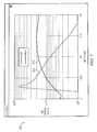
- FIG. 12is a chart 380 illustrating a substantial increase in R out range that is possible with reverse or forward bias voltages and shows dramatic changes with increasing or decreasing screen dopant density.
- This simulationuses an NMOS analog transistor similar to that simulated in FIG. 11 except for the additional screen layer and use of an undoped channel.
- Transistors created according to the foregoing embodimentswill have a reduced mismatch as compared to conventional MOS transistors.
- analog transistorsare often larger than digital transistors, since analog transistors and circuits are more affected by V t mismatch between identical devices.
- This V t variationdue in part to process variations in line etch roughness, oxide thickness, or gate granularity as well as more fundamental limitations such as random dopant fluctuations in nanometer sized channels, is more controllable for larger transistors.
- V t mismatch in small transistor devices built with a screen layer 112 and an undoped channel 110 as described hereincan effectively increase headroom which the devices have to operate. This allows high-bandwidth SoC devices with improved sensitivity and performance through improved V t matching and reduction in variation due to random dopant fluctuations that affect carrier mobility, capacitance, and other channel dependent transistor characteristics.
- wafers and die supporting multiple transistor typesincluding those with and without the described dopant structures, those having different threshold voltages, and with and without static or dynamic biasing, are contemplated.
- Electronic devices that include the disclosed transistor structurescan incorporate a die configured to operate as “systems on a chip” (SoC), advanced microprocessors, radio frequency, memory, and other die with one or more digital and analog transistor configurations and are capable of supporting a wide range of applications, including wireless telephones, communication devices, “smart phones”, embedded computers, portable computers, personal computers, servers, and other electronic devices.
- SoCsystem on a chip
- Electronic devicescan optionally include both conventional transistors and transistors as disclosed, either on the same die or connected to other die via motherboard, electrical or optical interconnect, stacking, or through use of 3D wafer bonding or packaging. According to the methods and processes discussed herein, a system having a variety of combinations of analog and/or digital transistor devices, channel lengths, and strain or other structures can be produced on silicon using planar bulk CMOS processing techniques. In different embodiments, the die may be divided into one or more areas where dynamic bias structures, static bias structures, or no-bias structures exist separately or in some combination.
Landscapes
- Insulated Gate Type Field-Effect Transistor (AREA)
- Metal-Oxide And Bipolar Metal-Oxide Semiconductor Integrated Circuits (AREA)
Abstract
Description
Claims (19)
Priority Applications (2)
| Application Number | Priority Date | Filing Date | Title |
|---|---|---|---|
| US13/553,902US8748270B1 (en) | 2011-03-30 | 2012-07-20 | Process for manufacturing an improved analog transistor |
| US14/273,938US9093469B2 (en) | 2011-03-30 | 2014-05-09 | Analog transistor |
Applications Claiming Priority (2)
| Application Number | Priority Date | Filing Date | Title |
|---|---|---|---|
| US201113076006A | 2011-03-30 | 2011-03-30 | |
| US13/553,902US8748270B1 (en) | 2011-03-30 | 2012-07-20 | Process for manufacturing an improved analog transistor |
Related Parent Applications (1)
| Application Number | Title | Priority Date | Filing Date |
|---|---|---|---|
| US201113076006ADivision | 2011-03-30 | 2011-03-30 |
Related Child Applications (1)
| Application Number | Title | Priority Date | Filing Date |
|---|---|---|---|
| US14/273,938ContinuationUS9093469B2 (en) | 2011-03-30 | 2014-05-09 | Analog transistor |
Publications (1)
| Publication Number | Publication Date |
|---|---|
| US8748270B1true US8748270B1 (en) | 2014-06-10 |
Family
ID=50845381
Family Applications (2)
| Application Number | Title | Priority Date | Filing Date |
|---|---|---|---|
| US13/553,902ActiveUS8748270B1 (en) | 2011-03-30 | 2012-07-20 | Process for manufacturing an improved analog transistor |
| US14/273,938ActiveUS9093469B2 (en) | 2011-03-30 | 2014-05-09 | Analog transistor |
Family Applications After (1)
| Application Number | Title | Priority Date | Filing Date |
|---|---|---|---|
| US14/273,938ActiveUS9093469B2 (en) | 2011-03-30 | 2014-05-09 | Analog transistor |
Country Status (1)
| Country | Link |
|---|---|
| US (2) | US8748270B1 (en) |
Cited By (17)
| Publication number | Priority date | Publication date | Assignee | Title |
|---|---|---|---|---|
| US20140091397A1 (en)* | 2012-10-02 | 2014-04-03 | Fujitsu Semiconductor Limited | Semiconductor integrated circuit device and method of manufacturing thereof |
| US20140248753A1 (en)* | 2011-03-30 | 2014-09-04 | Suvolta, Inc. | Analog transistor |
| US20150021681A1 (en)* | 2013-07-16 | 2015-01-22 | United Microelectronics Corp. | Semiconductor device having metal gate and manufacturing method thereof |
| US20150061012A1 (en)* | 2011-12-22 | 2015-03-05 | Suvolta, Inc. | High uniformity screen and epitaxial layers for cmos devices |
| US20150069500A1 (en)* | 2013-09-11 | 2015-03-12 | United Microelectronics Corporation | Vertical transistor device and fabricating method thereof |
| US20160336406A1 (en)* | 2015-05-15 | 2016-11-17 | Atomera, Incorporated | Semiconductor devices with superlattice and punch-through stop (pts) layers at different depths and related methods |
| US20170025501A1 (en)* | 2013-03-14 | 2017-01-26 | Mie Fujitsu Semiconductor Limited | Method for Fabricating a Transistor Device With a Tuned Dopant Profile |
| US20170125610A1 (en)* | 2015-10-30 | 2017-05-04 | Globalfoundries Inc. | Semiconductor structure including a varactor |
| US20170186852A1 (en)* | 2015-12-29 | 2017-06-29 | Globalfoundries Singapore Pte. Ltd. | Semiconductor device with improved narrow width effect and method of making thereof |
| US20170301694A1 (en)* | 2013-01-18 | 2017-10-19 | Renesas Electronics Corporation | Semiconductor device with silicon layer containing carbon |
| US20170323916A1 (en)* | 2013-05-24 | 2017-11-09 | Mie Fujitsu Semiconductor Limited | Buried Channel Deeply Depleted Channel Transistor |
| CN109841613A (en)* | 2017-11-27 | 2019-06-04 | 格芯公司 | The model of dynamic depleted transistor is generated using the system with analog circuit |
| US10431582B2 (en)* | 2016-05-31 | 2019-10-01 | Taiwan Semiconductor Manufacturing Company, Ltd. | High speed semiconductor device |
| US10522534B2 (en)* | 2016-04-29 | 2019-12-31 | Taiwan Semiconductor Manufacturing Co., Ltd. | FinFET varactor with low threshold voltage and method of making the same |
| US20220085155A1 (en)* | 2018-12-31 | 2022-03-17 | Unist(Ulsan National Institute Of Science And Technology) | Transistor device, ternary inverter device including same, and manufacturing method therefor |
| CN116190424A (en)* | 2022-10-25 | 2023-05-30 | 北京超弦存储器研究院 | Semiconductor device and manufacturing method thereof |
| US20240170575A1 (en)* | 2022-11-23 | 2024-05-23 | Globalfoundries U.S. Inc. | Gate structure over corner segment of semiconductor region |
Families Citing this family (2)
| Publication number | Priority date | Publication date | Assignee | Title |
|---|---|---|---|---|
| JP7091675B2 (en)* | 2018-01-26 | 2022-06-28 | ユナイテッド・セミコンダクター・ジャパン株式会社 | Semiconductor equipment |
| JP7115037B2 (en) | 2018-05-25 | 2022-08-09 | ユナイテッド・セミコンダクター・ジャパン株式会社 | semiconductor equipment |
Citations (455)
| Publication number | Priority date | Publication date | Assignee | Title |
|---|---|---|---|---|
| US3958266A (en) | 1974-04-19 | 1976-05-18 | Rca Corporation | Deep depletion insulated gate field effect transistors |
| US4000504A (en) | 1975-05-12 | 1976-12-28 | Hewlett-Packard Company | Deep channel MOS transistor |
| US4021835A (en) | 1974-01-25 | 1977-05-03 | Hitachi, Ltd. | Semiconductor device and a method for fabricating the same |
| US4242691A (en) | 1978-09-18 | 1980-12-30 | Mitsubishi Denki Kabushiki Kaisha | MOS Semiconductor device |
| US4276095A (en) | 1977-08-31 | 1981-06-30 | International Business Machines Corporation | Method of making a MOSFET device with reduced sensitivity of threshold voltage to source to substrate voltage variations |
| US4315781A (en) | 1980-04-23 | 1982-02-16 | Hughes Aircraft Company | Method of controlling MOSFET threshold voltage with self-aligned channel stop |
| US4518926A (en) | 1982-12-20 | 1985-05-21 | At&T Bell Laboratories | Gate-coupled field-effect transistor pair amplifier |
| US4559091A (en) | 1984-06-15 | 1985-12-17 | Regents Of The University Of California | Method for producing hyperabrupt doping profiles in semiconductors |
| US4578128A (en) | 1984-12-03 | 1986-03-25 | Ncr Corporation | Process for forming retrograde dopant distributions utilizing simultaneous outdiffusion of dopants |
| US4617066A (en) | 1984-11-26 | 1986-10-14 | Hughes Aircraft Company | Process of making semiconductors having shallow, hyperabrupt doped regions by implantation and two step annealing |
| US4662061A (en) | 1985-02-27 | 1987-05-05 | Texas Instruments Incorporated | Method for fabricating a CMOS well structure |
| US4761384A (en) | 1986-06-10 | 1988-08-02 | Siemens Aktiengesellschaft | Forming retrograde twin wells by outdiffusion of impurity ions in epitaxial layer followed by CMOS device processing |
| US4780748A (en) | 1986-06-06 | 1988-10-25 | American Telephone & Telegraph Company, At&T Bell Laboratories | Field-effect transistor having a delta-doped ohmic contact |
| US4819043A (en) | 1985-11-29 | 1989-04-04 | Hitachi, Ltd. | MOSFET with reduced short channel effect |
| EP0312237A2 (en) | 1987-10-13 | 1989-04-19 | AT&T Corp. | Interface charge enhancement in delta-doped heterostructure |
| US4885477A (en) | 1987-06-08 | 1989-12-05 | U.S. Philips Corporation | Differential amplifier and current sensing circuit including such an amplifier |
| US4908681A (en) | 1980-04-30 | 1990-03-13 | Sanyo Electric Co., Ltd. | Insulated gate field effect transistor with buried layer |
| US4945254A (en) | 1986-03-19 | 1990-07-31 | The Secretary of State for Defence in Her Britannic Majesty's Government for the United Kingdom of Great Britain and Northern Ireland | Method and apparatus for monitoring surface layer growth |
| US4956311A (en) | 1989-06-27 | 1990-09-11 | National Semiconductor Corporation | Double-diffused drain CMOS process using a counterdoping technique |
| US5034337A (en) | 1989-02-10 | 1991-07-23 | Texas Instruments Incorporated | Method of making an integrated circuit that combines multi-epitaxial power transistors with logic/analog devices |
| US5144378A (en) | 1990-03-06 | 1992-09-01 | Fujitsu Limited | High electron mobility transistor |
| US5156990A (en) | 1986-07-23 | 1992-10-20 | Texas Instruments Incorporated | Floating-gate memory cell with tailored doping profile |
| US5156989A (en) | 1988-11-08 | 1992-10-20 | Siliconix, Incorporated | Complementary, isolated DMOS IC technology |
| US5166765A (en) | 1991-08-26 | 1992-11-24 | At&T Bell Laboratories | Insulated gate field-effect transistor with pulse-shaped doping |
| US5208473A (en) | 1989-11-29 | 1993-05-04 | Mitsubishi Denki Kabushiki Kaisha | Lightly doped MISFET with reduced latchup and punchthrough |
| US5294821A (en) | 1990-10-09 | 1994-03-15 | Seiko Epson Corporation | Thin-film SOI semiconductor device having heavily doped diffusion regions beneath the channels of transistors |
| US5298763A (en) | 1992-11-02 | 1994-03-29 | Motorola, Inc. | Intrinsically doped semiconductor structure and method for making |
| EP0274278B1 (en) | 1987-01-05 | 1994-05-25 | Seiko Instruments Inc. | MOS field effect transistor and method of manufacturing the same |
| US5369288A (en) | 1992-05-08 | 1994-11-29 | Fujitsu Limited | Semiconductor device for switching a ballistic flow of carriers |
| US5373186A (en) | 1984-11-19 | 1994-12-13 | Max-Planck Gesellschaft Zur Foerderung Der Wissenschaften E.V. | Bipolar transistor with monoatomic base layer between emitter and collector layers |
| US5384476A (en) | 1979-08-25 | 1995-01-24 | Zaidan Hojin Handotai Kenkyu Shinkokai | Short channel MOSFET with buried anti-punch through region |
| US5426328A (en) | 1992-09-21 | 1995-06-20 | Siliconix Incorporated | BICDMOS structures |
| US5444008A (en) | 1993-09-24 | 1995-08-22 | Vlsi Technology, Inc. | High-performance punchthrough implant method for MOS/VLSI |
| EP0531621A3 (en) | 1991-09-12 | 1995-08-30 | Po Hang Iron & Steel | Process for formation of delta-doped quantum well field effect transistor |
| US5552332A (en) | 1995-06-02 | 1996-09-03 | Motorola, Inc. | Process for fabricating a MOSFET device having reduced reverse short channel effects |
| US5559368A (en) | 1994-08-30 | 1996-09-24 | The Regents Of The University Of California | Dynamic threshold voltage mosfet having gate to body connection for ultra-low voltage operation |
| US5608253A (en) | 1995-03-22 | 1997-03-04 | Advanced Micro Devices Inc. | Advanced transistor structures with optimum short channel controls for high density/high performance integrated circuits |
| US5622880A (en) | 1994-08-18 | 1997-04-22 | Sun Microsystems, Inc. | Method of making a low power, high performance junction transistor |
| US5625568A (en) | 1993-12-22 | 1997-04-29 | Vlsi Technology, Inc. | Method and apparatus for compacting integrated circuits with standard cell architectures |
| US5624863A (en) | 1995-07-17 | 1997-04-29 | Micron Technology, Inc. | Semiconductor processing method of forming complementary N-type doped and P-type doped active regions within a semiconductor substrate |
| US5641980A (en) | 1995-06-16 | 1997-06-24 | Mitsubishi Denki Kabushiki Kaisha | Device having a high concentration region under the channel |
| US5663583A (en) | 1995-06-06 | 1997-09-02 | Hughes Aircraft Company | Low-noise and power ALGaPSb/GaInAs HEMTs and pseudomorpohic HEMTs on GaAs substrate |
| US5712501A (en) | 1995-10-10 | 1998-01-27 | Motorola, Inc. | Graded-channel semiconductor device |
| US5726562A (en) | 1995-09-07 | 1998-03-10 | Nec Corporation | Semiconductor device and power supply controller for same |
| US5726488A (en) | 1985-11-29 | 1998-03-10 | Hitachi, Ltd. | Semiconductor device having semiconductor elements formed in a retrograde well structure |
| US5731626A (en) | 1994-12-01 | 1998-03-24 | Lucent Technologies Inc. | Process for controlling dopant diffusion in a semiconductor layer and semiconductor layer formed thereby |
| US5736419A (en) | 1996-11-12 | 1998-04-07 | National Semiconductor Corporation | Method of fabricating a raised source/drain MOSFET using self-aligned POCl3 for doping gate/source/drain regions |
| US5753555A (en) | 1995-11-22 | 1998-05-19 | Nec Corporation | Method for forming semiconductor device |
| US5754826A (en) | 1995-08-04 | 1998-05-19 | Synopsys, Inc. | CAD and simulation system for targeting IC designs to multiple fabrication processes |
| US5756365A (en) | 1992-10-30 | 1998-05-26 | Kabushiki Kaisha Toshiba | Method of manufacturing MOS-type semiconductor device having electrode structure capable of coping with short-channel effects |
| US5763921A (en) | 1991-10-22 | 1998-06-09 | Mitsubishi Denki Kabushiki Kaisha | Semiconductor device including retrograde well structure with suppressed substrate bias effects |
| US5847419A (en) | 1996-09-17 | 1998-12-08 | Kabushiki Kaisha Toshiba | Si-SiGe semiconductor device and method of fabricating the same |
| US5856003A (en) | 1997-11-17 | 1999-01-05 | Taiwan Semiconductor Manufacturing Company, Ltd. | Method for forming pseudo buried layer for sub-micron bipolar or BiCMOS device |
| US5861334A (en) | 1995-08-07 | 1999-01-19 | Hyundai Electronics Industries Co., | Method for fabricating semiconductor device having a buried channel |
| US5885876A (en) | 1996-02-07 | 1999-03-23 | Thunderbird Technologies, Inc. | Methods of fabricating short channel fermi-threshold field effect transistors including drain field termination region |
| US5889315A (en) | 1994-08-18 | 1999-03-30 | National Semiconductor Corporation | Semiconductor structure having two levels of buried regions |
| US5895954A (en) | 1997-03-27 | 1999-04-20 | Mitsubishi Denki Kabushiki Kaisha | Field effect transistor with impurity concentration peak under gate electrode |
| US5918129A (en) | 1997-02-25 | 1999-06-29 | Advanced Micro Devices, Inc. | Method of channel doping using diffusion from implanted polysilicon |
| US5923987A (en) | 1997-06-30 | 1999-07-13 | Sun Microsystems, Inc. | Method for forming MOS devices with retrograde pocket regions and counter dopant regions at the substrate surface |
| US5923067A (en) | 1997-04-04 | 1999-07-13 | International Business Machines Corporation | 3-D CMOS-on-SOI ESD structure and method |
| US5936868A (en) | 1997-03-06 | 1999-08-10 | Harris Corporation | Method for converting an integrated circuit design for an upgraded process |
| US5946214A (en) | 1997-07-11 | 1999-08-31 | Advanced Micro Devices | Computer implemented method for estimating fabrication yield for semiconductor integrated circuit including memory blocks with redundant rows and/or columns |
| US5985705A (en) | 1998-06-30 | 1999-11-16 | Lsi Logic Corporation | Low threshold voltage MOS transistor and method of manufacture |
| US5989963A (en) | 1997-07-21 | 1999-11-23 | Advanced Micro Devices, Inc. | Method for obtaining a steep retrograde channel profile |
| US6001695A (en) | 1998-03-02 | 1999-12-14 | Texas Instruments - Acer Incorporated | Method to form ultra-short channel MOSFET with a gate-side airgap structure |
| US6020227A (en) | 1995-09-12 | 2000-02-01 | National Semiconductor Corporation | Fabrication of multiple field-effect transistor structure having local threshold-adjust doping |
| US6060364A (en) | 1999-03-02 | 2000-05-09 | Advanced Micro Devices, Inc. | Fast Mosfet with low-doped source/drain |
| US6060345A (en) | 1997-04-21 | 2000-05-09 | Advanced Micro Devices, Inc. | Method of making NMOS and PMOS devices with reduced masking steps |
| US6066533A (en) | 1998-09-29 | 2000-05-23 | Advanced Micro Devices, Inc. | MOS transistor with dual metal gate structure |
| US6072217A (en) | 1998-06-11 | 2000-06-06 | Sun Microsystems, Inc. | Tunable threshold SOI device using isolated well structure for back gate |
| US6087691A (en) | 1997-02-04 | 2000-07-11 | Mitsubishi Denki Kabushiki Kaisha | Semiconductor device having lower minority carrier noise |
| US6088518A (en) | 1998-01-30 | 2000-07-11 | Aspec Technology, Inc. | Method and system for porting an integrated circuit layout from a reference process to a target process |
| US6087210A (en) | 1998-06-05 | 2000-07-11 | Hyundai Electronics Industries | Method of manufacturing a CMOS Transistor |
| US6091286A (en) | 1994-02-14 | 2000-07-18 | Philips Electronics North America Corporation | Fully integrated reference circuit having controlled temperature dependence |
| US6096611A (en) | 1998-03-13 | 2000-08-01 | Texas Instruments - Acer Incorporated | Method to fabricate dual threshold CMOS circuits |
| US6103562A (en) | 1998-01-14 | 2000-08-15 | Lg Semicon Co., Ltd. | Method of making semiconductor device with decreased channel width and constant threshold voltage |
| US6121153A (en) | 1994-08-29 | 2000-09-19 | Fujitsu Limited | Semiconductor device having a regrowth crystal region |
| US6147383A (en) | 1995-03-10 | 2000-11-14 | Sony Corporation | LDD buried channel field effect semiconductor device and manufacturing method |
| US6153920A (en) | 1994-12-01 | 2000-11-28 | Lucent Technologies Inc. | Process for controlling dopant diffusion in a semiconductor layer and semiconductor device formed thereby |
| US6157073A (en) | 1997-09-29 | 2000-12-05 | Stmicroelectronics S.A. | Isolation between power supplies of an analog-digital circuit |
| US6175582B1 (en) | 1997-11-26 | 2001-01-16 | Mitsui Chemicals Inc. | Semiconductor laser device |
| US6184112B1 (en) | 1998-12-02 | 2001-02-06 | Advanced Micro Devices, Inc. | Method of forming a MOSFET transistor with a shallow abrupt retrograde dopant profile |
| US6190979B1 (en) | 1999-07-12 | 2001-02-20 | International Business Machines Corporation | Method for fabricating dual workfunction devices on a semiconductor substrate using counter-doping and gapfill |
| US6194259B1 (en) | 1997-06-27 | 2001-02-27 | Advanced Micro Devices, Inc. | Forming retrograde channel profile and shallow LLDD/S-D extensions using nitrogen implants |
| US6198157B1 (en) | 1997-02-26 | 2001-03-06 | Hitachi, Ltd. | Semiconductor device having buried boron and carbon regions |
| US6218895B1 (en) | 1997-06-20 | 2001-04-17 | Intel Corporation | Multiple well transistor circuits having forward body bias |
| US6218892B1 (en) | 1997-06-20 | 2001-04-17 | Intel Corporation | Differential circuits employing forward body bias |
| US6221724B1 (en) | 1998-11-06 | 2001-04-24 | Advanced Micro Devices, Inc. | Method of fabricating an integrated circuit having punch-through suppression |
| US6232164B1 (en) | 1999-05-24 | 2001-05-15 | Taiwan Semiconductor Manufacturing Company | Process of making CMOS device structure having an anti-SCE block implant |
| US6235597B1 (en) | 1999-08-06 | 2001-05-22 | International Business Machines Corporation | Semiconductor structure having reduced silicide resistance between closely spaced gates and method of fabrication |
| US6245618B1 (en) | 1999-02-03 | 2001-06-12 | Advanced Micro Devices, Inc. | Mosfet with localized amorphous region with retrograde implantation |
| US6268640B1 (en) | 1999-08-12 | 2001-07-31 | International Business Machines Corporation | Forming steep lateral doping distribution at source/drain junctions |
| US6271070B2 (en) | 1997-12-25 | 2001-08-07 | Matsushita Electronics Corporation | Method of manufacturing semiconductor device |
| US6271551B1 (en) | 1995-12-15 | 2001-08-07 | U.S. Philips Corporation | Si-Ge CMOS semiconductor device |
| US20010014495A1 (en) | 1999-01-27 | 2001-08-16 | Bin Yu | Method for forming super-steep retrograded channel (SSRC) for cmos transistor using rapid laser annealing to reduce thermal budget |
| EP0683515B1 (en) | 1994-05-17 | 2001-08-16 | Samsung Electronics Co., Ltd. | Method of manufacturing a CMOS device |
| US6288429B1 (en) | 1996-12-04 | 2001-09-11 | Sharp Kabushiki Kaisha | Semiconductor device |
| US6297132B1 (en) | 2000-02-07 | 2001-10-02 | Chartered Semiconductor Manufacturing Ltd. | Process to control the lateral doping profile of an implanted channel region |
| US6300177B1 (en) | 2001-01-25 | 2001-10-09 | Chartered Semiconductor Manufacturing Inc. | Method to form transistors with multiple threshold voltages (VT) using a combination of different work function gate materials |
| US6313489B1 (en) | 1999-11-16 | 2001-11-06 | Philips Electronics North America Corporation | Lateral thin-film silicon-on-insulator (SOI) device having a lateral drift region with a retrograde doping profile, and method of making such a device |
| US6320222B1 (en) | 1998-09-01 | 2001-11-20 | Micron Technology, Inc. | Structure and method for reducing threshold voltage variations due to dopant fluctuations |
| US6319799B1 (en) | 2000-05-09 | 2001-11-20 | Board Of Regents, The University Of Texas System | High mobility heterojunction transistor and method |
| US6323525B1 (en) | 1997-09-18 | 2001-11-27 | Kabushiki Kaisha Toshiba | MISFET semiconductor device having relative impurity concentration levels between layers |
| US6326666B1 (en) | 2000-03-23 | 2001-12-04 | International Business Machines Corporation | DTCMOS circuit having improved speed |
| US6335233B1 (en) | 1998-07-02 | 2002-01-01 | Samsung Electronics Co., Ltd. | Method for fabricating MOS transistor |
| US6358806B1 (en) | 2001-06-29 | 2002-03-19 | Lsi Logic Corporation | Silicon carbide CMOS channel |
| US20020042184A1 (en) | 2000-10-10 | 2002-04-11 | Mahalingam Nandakumar | Reduction in well implant channeling and resulting latchup characteristics in shallow trench ilolation by implanting wells through nitride |
| US6380019B1 (en) | 1998-11-06 | 2002-04-30 | Advanced Micro Devices, Inc. | Method of manufacturing a transistor with local insulator structure |
| US6391752B1 (en) | 2000-09-12 | 2002-05-21 | Taiwan Semiconductor Manufacturing, Co., Ltd. | Method of fabricating a silicon-on-insulator semiconductor device with an implanted ground plane |
| US6426279B1 (en) | 1999-08-18 | 2002-07-30 | Advanced Micro Devices, Inc. | Epitaxial delta doping for retrograde channel profile |
| US6426260B1 (en) | 1997-12-02 | 2002-07-30 | Magepower Semiconductor Corp. | Switching speed improvement in DMO by implanting lightly doped region under gate |
| US6432754B1 (en) | 2001-02-20 | 2002-08-13 | International Business Machines Corporation | Double SOI device with recess etch and epitaxy |
| US6444551B1 (en) | 2001-07-23 | 2002-09-03 | Taiwan Semiconductor Manufacturing Company | N-type buried layer drive-in recipe to reduce pits over buried antimony layer |
| US6444550B1 (en) | 1999-08-18 | 2002-09-03 | Advanced Micro Devices, Inc. | Laser tailoring retrograde channel profile in surfaces |
| US6449749B1 (en) | 1999-11-18 | 2002-09-10 | Pdf Solutions, Inc. | System and method for product yield prediction |
| US6461928B2 (en) | 2000-05-23 | 2002-10-08 | Texas Instruments Incorporated | Methodology for high-performance, high reliability input/output devices and analog-compatible input/output and core devices using core device implants |
| US6461920B1 (en) | 1996-04-01 | 2002-10-08 | Mitsubishi Denki Kabushiki Kaisha | Semiconductor device and method of manufacturing the same |
| US6472278B1 (en) | 1998-06-22 | 2002-10-29 | Motorola, Inc. | Method and apparatus for creating a voltage threshold in a FET |
| US6482714B1 (en) | 1999-02-24 | 2002-11-19 | Kabushiki Kaisha Toshiba | Semiconductor device and method of manufacturing the same |
| US6489224B1 (en) | 2001-05-31 | 2002-12-03 | Sun Microsystems, Inc. | Method for engineering the threshold voltage of a device using buried wells |
| US6492232B1 (en) | 1998-06-15 | 2002-12-10 | Motorola, Inc. | Method of manufacturing vertical semiconductor device |
| US6500739B1 (en) | 2001-06-14 | 2002-12-31 | Taiwan Semiconductor Manufacturing Company | Formation of an indium retrograde profile via antimony ion implantation to improve NMOS short channel effect |
| US6503801B1 (en) | 1999-08-18 | 2003-01-07 | Advanced Micro Devices, Inc. | Non-uniform channel profile via enhanced diffusion |
| US6503805B2 (en) | 1999-09-02 | 2003-01-07 | Micron Technology, Inc. | Channel implant through gate polysilicon |
| US20030006415A1 (en) | 2000-06-27 | 2003-01-09 | Toshiya Yokogawa | Semiconductor device |
| US6506640B1 (en) | 1999-09-24 | 2003-01-14 | Advanced Micro Devices, Inc. | Multiple channel implantation to form retrograde channel profile and to engineer threshold voltage and sub-surface punch-through |
| US6518623B1 (en) | 2000-06-09 | 2003-02-11 | Mitsubishi Denki Kabushiki Kaisha | Semiconductor device having a buried-channel MOS structure |
| US6521470B1 (en) | 2001-10-31 | 2003-02-18 | United Microelectronics Corp. | Method of measuring thickness of epitaxial layer |
| US6534373B1 (en) | 2001-03-26 | 2003-03-18 | Advanced Micro Devices, Inc. | MOS transistor with reduced floating body effect |
| US6541328B2 (en) | 2001-02-19 | 2003-04-01 | Samsung Electronics Co., Ltd. | Method of fabricating metal oxide semiconductor transistor with lightly doped impurity regions formed after removing spacers used for defining higher density impurity regions |
| US6541829B2 (en) | 1999-12-03 | 2003-04-01 | Kabushiki Kaisha Toshiba | Semiconductor device and method of manufacturing the same |
| US6548842B1 (en) | 2000-03-31 | 2003-04-15 | National Semiconductor Corporation | Field-effect transistor for alleviating short-channel effects |
| US6551885B1 (en) | 2001-02-09 | 2003-04-22 | Advanced Micro Devices, Inc. | Low temperature process for a thin film transistor |
| US6573129B2 (en) | 1999-08-06 | 2003-06-03 | Raytheon Company | Gate electrode formation in double-recessed transistor by two-step etching |
| US6576535B2 (en) | 2001-04-11 | 2003-06-10 | Texas Instruments Incorporated | Carbon doped epitaxial layer for high speed CB-CMOS |
| US6600200B1 (en) | 1999-08-25 | 2003-07-29 | Infineon Technologies Ag | MOS transistor, method for fabricating a MOS transistor and method for fabricating two complementary MOS transistors |
| US6620671B1 (en) | 2001-05-01 | 2003-09-16 | Advanced Micro Devices, Inc. | Method of fabricating transistor having a single crystalline gate conductor |
| US20030173626A1 (en) | 2001-05-18 | 2003-09-18 | Burr James B. | Device including a resistive path to introduce an equivalent RC circuit |
| US6624488B1 (en) | 2000-08-07 | 2003-09-23 | Advanced Micro Devices, Inc. | Epitaxial silicon growth and usage of epitaxial gate insulator for low power, high performance devices |
| US6627473B1 (en) | 1999-11-16 | 2003-09-30 | Nec Compound Semiconductor Devices, Ltd. | Compound semiconductor device with delta doped layer under etching stopper layer for decreasing resistance between active layer and ohmic electrode and process of fabrication thereof |
| US20030183856A1 (en) | 2002-03-28 | 2003-10-02 | Karsten Wieczorek | Semiconductor device having a retrograde dopant profile in a channel region and method for fabricating the same |
| US6630710B1 (en) | 1998-09-29 | 2003-10-07 | Newport Fab, Llc | Elevated channel MOSFET |
| US20030215992A1 (en) | 2002-05-20 | 2003-11-20 | Sohn Yong Sun | Method for forming transistor of semiconductor device |
| US6660605B1 (en) | 2002-11-12 | 2003-12-09 | Texas Instruments Incorporated | Method to fabricate optimal HDD with dual diffusion process to optimize transistor drive current junction capacitance, tunneling current and channel dopant loss |
| US6662350B2 (en) | 2002-01-28 | 2003-12-09 | International Business Machines Corporation | FinFET layout generation |
| US6670260B1 (en) | 1998-11-06 | 2003-12-30 | Advanced Micro Devices, Inc. | Transistor with local insulator structure |
| US6693333B1 (en) | 2001-05-01 | 2004-02-17 | Advanced Micro Devices, Inc. | Semiconductor-on-insulator circuit with multiple work functions |
| JP2004087671A (en) | 2002-08-26 | 2004-03-18 | Sharp Corp | Semiconductor device and method of manufacturing the same |
| US20040075118A1 (en) | 2000-12-08 | 2004-04-22 | Bernd Heinemann | Layers in substrate wafers |
| US20040075143A1 (en) | 2000-01-07 | 2004-04-22 | Geum-Jong Bae | CMOS integrated circuit devices and substrates having buried silicon germanium layers therein and methods of forming same |
| US6730568B2 (en) | 2002-09-17 | 2004-05-04 | Hynix Semiconductor Inc. | Method for fabricating semiconductor device with ultra-shallow super-steep-retrograde epi-channel by boron-fluoride compound doping |
| US20040087090A1 (en) | 2002-10-31 | 2004-05-06 | Grudowski Paul A. | Semiconductor fabrication process using transistor spacers of differing widths |
| US20040084731A1 (en) | 2001-03-29 | 2004-05-06 | Kabushiki Kaisha Toshiba | Semiconductor device comprising buried channel region and method for manufacturing the same |
| US6743291B2 (en) | 2002-07-09 | 2004-06-01 | Chartered Semiconductor Manufacturing Ltd. | Method of fabricating a CMOS device with integrated super-steep retrograde twin wells using double selective epitaxial growth |
| US6743684B2 (en) | 2002-10-11 | 2004-06-01 | Texas Instruments Incorporated | Method to produce localized halo for MOS transistor |
| US6751519B1 (en) | 2001-10-25 | 2004-06-15 | Kla-Tencor Technologies Corporation | Methods and systems for predicting IC chip yield |
| US6753230B2 (en) | 2002-05-18 | 2004-06-22 | Hynix Semiconductor Inc. | Method for fabricating semiconductor device with ultra-shallow super-steep-retrograde epi-channel by decaborane doping |
| US20040126947A1 (en) | 2002-12-30 | 2004-07-01 | Hynix Semiconductor Inc. | pMOS device having ultra shallow super-steep-retrograde epi-channel with dual channel doping and method for fabricating the same |
| US6760900B2 (en) | 2001-12-03 | 2004-07-06 | Anadigics Inc. | Integrated circuits with scalable design |
| US6787424B1 (en) | 2001-02-09 | 2004-09-07 | Advanced Micro Devices, Inc. | Fully depleted SOI transistor with elevated source and drain |
| US20040175893A1 (en) | 2003-03-07 | 2004-09-09 | Applied Materials, Inc. | Apparatuses and methods for forming a substantially facet-free epitaxial film |
| US20040180488A1 (en) | 2003-03-13 | 2004-09-16 | Won-Ho Lee | Method for fabricating complementary metal oxide semiconductor image sensor |
| US6797602B1 (en) | 2001-02-09 | 2004-09-28 | Advanced Micro Devices, Inc. | Method of manufacturing a semiconductor device with supersaturated source/drain extensions and metal silicide contacts |
| US6797553B2 (en) | 2000-10-24 | 2004-09-28 | International Business Machines Corporation | Method for making multiple threshold voltage FET using multiple work-function gate materials |
| US6797994B1 (en) | 2000-02-14 | 2004-09-28 | Raytheon Company | Double recessed transistor |
| US6808004B2 (en) | 2002-01-31 | 2004-10-26 | Tht Presses Inc. | Semi-solid molding method |
| US6808994B1 (en) | 2003-06-17 | 2004-10-26 | Micron Technology, Inc. | Transistor structures and processes for forming same |
| US6813750B2 (en) | 2001-04-02 | 2004-11-02 | Kabushiki Kaisha Toshiba | Logic circuit design equipment and method for designing logic circuit for reducing leakage current |
| US6821852B2 (en) | 2001-02-13 | 2004-11-23 | Micron Technology, Inc. | Dual doped gates |
| US6821825B2 (en) | 2001-02-12 | 2004-11-23 | Asm America, Inc. | Process for deposition of semiconductor films |
| US6822297B2 (en) | 2001-06-07 | 2004-11-23 | Texas Instruments Incorporated | Additional n-type LDD/pocket implant for improving short-channel NMOS ESD robustness |
| US6831292B2 (en) | 2001-09-21 | 2004-12-14 | Amberwave Systems Corporation | Semiconductor structures employing strained material layers with defined impurity gradients and methods for fabricating same |
| US6835639B2 (en) | 2001-11-30 | 2004-12-28 | Texas Instruments Incorporated | Multiple work function gates |
| US6852602B2 (en) | 2001-01-31 | 2005-02-08 | Matsushita Electric Industrial Co., Ltd. | Semiconductor crystal film and method for preparation thereof |
| US6852603B2 (en) | 2001-12-12 | 2005-02-08 | Texas Instruments Incorporated | Fabrication of abrupt ultra-shallow junctions |
| US6891439B2 (en) | 2002-11-04 | 2005-05-10 | Advanced Micro Devices, Inc. | Circuit and a method for controlling the bias current in a switched capacitor circuit |
| US6893947B2 (en) | 2002-06-25 | 2005-05-17 | Freescale Semiconductor, Inc. | Advanced RF enhancement-mode FETs with improved gate properties |
| US20050106824A1 (en) | 2001-12-04 | 2005-05-19 | Carnera Alberto | Method for suppressing transient enhanced diffusion of dopants in silicon |
| US6900519B2 (en) | 2002-07-18 | 2005-05-31 | International Business Machines Corporation | Diffused extrinsic base and method for fabrication |
| US20050116282A1 (en) | 2003-12-02 | 2005-06-02 | Vishay-Siliconix | Closed cell trench metal-oxide-semiconductor field effect transistor |
| US6916698B2 (en) | 2002-04-19 | 2005-07-12 | International Business Machines Corporation | High performance CMOS device structure with mid-gap metal gate |
| US6917237B1 (en) | 2004-03-02 | 2005-07-12 | Intel Corporation | Temperature dependent regulation of threshold voltage |
| US6927463B2 (en) | 1996-06-28 | 2005-08-09 | Sharp Kabushiki Kaisha | Semiconductor device and method for fabricating the same |
| US6928128B1 (en) | 1999-05-03 | 2005-08-09 | Rambus Inc. | Clock alignment circuit having a self regulating voltage supply |
| US6930360B2 (en) | 2002-09-24 | 2005-08-16 | Kabushiki Kaisha Toshiba | Semiconductor device and manufacturing method of the same |
| US6930007B2 (en) | 2003-09-15 | 2005-08-16 | Texas Instruments Incorporated | Integration of pre-S/D anneal selective nitride/oxide composite cap for improving transistor performance |
| US6957163B2 (en) | 2002-04-24 | 2005-10-18 | Yoshiyuki Ando | Integrated circuits having post-silicon adjustment control |
| US6963090B2 (en) | 2003-01-09 | 2005-11-08 | Freescale Semiconductor, Inc. | Enhancement mode metal-oxide-semiconductor field effect transistor |
| US20050250289A1 (en) | 2002-10-30 | 2005-11-10 | Babcock Jeffrey A | Control of dopant diffusion from buried layers in bipolar integrated circuits |
| US20050280075A1 (en) | 2003-06-10 | 2005-12-22 | Fujitsu Limited | Semiconductor integrated circuit device having improved punch-through resistance and production method thereof, semiconductor integrated circuit device including a low-voltage transistor and a high-voltage transistor |
| US20060022270A1 (en) | 2004-07-30 | 2006-02-02 | International Business Machines Corporation | Ultra-thin body super-steep retrograde well (ssrw) fet devices |
| US6995397B2 (en) | 2001-09-14 | 2006-02-07 | Matsushita Electric Industrial Co., Ltd. | Semiconductor device |
| US7008836B2 (en) | 2003-03-28 | 2006-03-07 | Infineon Technologies Wireless Solutions Sweden Ab | Method to provide a triple well in an epitaxially based CMOS or BiCMOS process |
| US20060049464A1 (en) | 2004-09-03 | 2006-03-09 | Rao G R Mohan | Semiconductor devices with graded dopant regions |
| US7013359B1 (en) | 2001-12-21 | 2006-03-14 | Cypress Semiconductor Corporation | High speed memory interface system and method |
| US7015546B2 (en) | 2000-02-23 | 2006-03-21 | Semiconductor Research Corporation | Deterministically doped field-effect devices and methods of making same |
| US7015741B2 (en) | 2003-12-23 | 2006-03-21 | Intel Corporation | Adaptive body bias for clock skew compensation |
| US20060068586A1 (en) | 2004-09-17 | 2006-03-30 | Bedabrata Pain | Method for implementation of back-illuminated CMOS or CCD imagers |
| US20060068555A1 (en) | 2004-09-30 | 2006-03-30 | International Business Machines Corporation | Structure and method for manufacturing MOSFET with super-steep retrograded island |
| US7022559B2 (en) | 1998-09-30 | 2006-04-04 | Intel Corporation | MOSFET gate electrodes having performance tuned work functions and methods of making same |
| US20060071278A1 (en) | 2004-09-27 | 2006-04-06 | Fujitsu Limited | Semiconductor device and method for fabricating the same |
| US7036098B2 (en) | 2003-06-30 | 2006-04-25 | Sun Microsystems, Inc. | On-chip signal state duration measurement and adjustment |
| US7039881B2 (en) | 1999-12-08 | 2006-05-02 | Timothy James Regan | Modification of integrated circuits |
| US7038258B2 (en) | 2003-06-05 | 2006-05-02 | Texas Instruments Incorporated | Semiconductor device having a localized halo implant therein and method of manufacture therefor |
| US7045456B2 (en) | 2003-12-22 | 2006-05-16 | Texas Instruments Incorporated | MOS transistor gates with thin lower metal silicide and methods for making the same |
| US7057216B2 (en) | 2003-10-31 | 2006-06-06 | International Business Machines Corporation | High mobility heterojunction complementary field effect transistors and methods thereof |
| US7061058B2 (en) | 2003-12-01 | 2006-06-13 | Texas Instruments Incorporated | Forming a retrograde well in a transistor to enhance performance of the transistor |
| US7064399B2 (en) | 2000-09-15 | 2006-06-20 | Texas Instruments Incorporated | Advanced CMOS using super steep retrograde wells |
| US7071103B2 (en) | 2004-07-30 | 2006-07-04 | International Business Machines Corporation | Chemical treatment to retard diffusion in a semiconductor overlayer |
| US20060154428A1 (en) | 2005-01-12 | 2006-07-13 | International Business Machines Corporation | Increasing doping of well compensating dopant region according to increasing gate length |
| US7078325B2 (en) | 2000-07-12 | 2006-07-18 | Infineon Technologies Ag | Process for producing a doped semiconductor substrate |
| US7089515B2 (en) | 2004-03-09 | 2006-08-08 | International Business Machines Corporation | Threshold voltage roll-off compensation using back-gated MOSFET devices for system high-performance and low standby power |
| US7089513B2 (en) | 2004-03-19 | 2006-08-08 | International Business Machines Corporation | Integrated circuit design for signal integrity, avoiding well proximity effects |
| US7091093B1 (en) | 1999-09-17 | 2006-08-15 | Matsushita Electric Industrial Co., Ltd. | Method for fabricating a semiconductor device having a pocket dopant diffused layer |
| US7105399B1 (en) | 2004-12-07 | 2006-09-12 | Advanced Micro Devices, Inc. | Selective epitaxial growth for tunable channel thickness |
| US20060203581A1 (en) | 2005-03-10 | 2006-09-14 | Joshi Rajiv V | Efficient method and computer program for modeling and improving static memory performance across process variations and environmental conditions |
| US7109099B2 (en) | 2003-10-17 | 2006-09-19 | Chartered Semiconductor Manufacturing Ltd. | End of range (EOR) secondary defect engineering using substitutional carbon doping |
| US20060223248A1 (en) | 2005-03-29 | 2006-10-05 | Texas Instruments Incorporated | N+ poly on high-k dielectric for semiconductor devices |
| US20060220114A1 (en) | 2005-03-30 | 2006-10-05 | Fujitsu Limited | Semiconductor device and manufacturing method thereof |
| US7119381B2 (en) | 2004-07-30 | 2006-10-10 | Freescale Semiconductor, Inc. | Complementary metal-oxide-semiconductor field effect transistor structure having ion implant in only one of the complementary devices |
| US7122411B2 (en) | 2000-08-31 | 2006-10-17 | Micron Technology, Inc | SOI device with reduced drain induced barrier lowering |
| US7127687B1 (en) | 2003-10-14 | 2006-10-24 | Sun Microsystems, Inc. | Method and apparatus for determining transistor sizes |
| US7132323B2 (en) | 2003-11-14 | 2006-11-07 | International Business Machines Corporation | CMOS well structure and method of forming the same |
| EP0889502B1 (en) | 1997-06-30 | 2006-12-20 | International Business Machines Corporation | Semiconductor structure with abrupt doping profile |
| US7170120B2 (en) | 2005-03-31 | 2007-01-30 | Intel Corporation | Carbon nanotube energy well (CNEW) field effect transistor |
| US7169675B2 (en) | 2004-07-07 | 2007-01-30 | Chartered Semiconductor Manufacturing, Ltd | Material architecture for the fabrication of low temperature transistor |
| US7176137B2 (en) | 2003-05-09 | 2007-02-13 | Taiwan Semiconductor Manufacturing Co., Ltd. | Method for multiple spacer width control |
| US20070040222A1 (en) | 2005-06-15 | 2007-02-22 | Benjamin Van Camp | Method and apparatus for improved ESD performance |
| US7189627B2 (en) | 2004-08-19 | 2007-03-13 | Texas Instruments Incorporated | Method to improve SRAM performance and stability |
| US7202517B2 (en) | 2003-07-18 | 2007-04-10 | Interuniversitair Microelektronica Centrum (Imec Vzw) | Multiple gate semiconductor device and method for forming same |
| US7208354B2 (en) | 2003-07-23 | 2007-04-24 | Asm America, Inc. | Deposition of silicon germanium on silicon-on-insulator structures and bulk substrates |
| US7211871B2 (en) | 2003-12-31 | 2007-05-01 | Dongbu Electronics, Co., Ltd. | Transistors of semiconductor devices and methods of fabricating the same |
| US7221021B2 (en) | 2004-06-25 | 2007-05-22 | Taiwan Semiconductor Manufacturing Co., Ltd. | Method of forming high voltage devices with retrograde well |
| US7226843B2 (en) | 2002-09-30 | 2007-06-05 | Intel Corporation | Indium-boron dual halo MOSFET |
| US7226833B2 (en) | 2004-10-29 | 2007-06-05 | Freescale Semiconductor, Inc. | Semiconductor device structure and method therefor |
| US7230680B2 (en) | 2002-12-20 | 2007-06-12 | Kabushiki Kaisha Toshiba | Wafer flatness evaluation method, wafer flatness evaluation apparatus carrying out the evaluation method, wafer manufacturing method using the evaluation method, wafer quality assurance method using the evaluation method, semiconductor device manufacturing method using the evaluation method and semiconductor device manufacturing method using a wafer evaluated by the evaluation method |
| US7235822B2 (en) | 2003-12-30 | 2007-06-26 | Infineon Technologies Ag | Transistor with silicon and carbon layer in the channel region |
| US7256639B1 (en) | 2004-02-02 | 2007-08-14 | Transmeta Corporation | Systems and methods for integrated circuits comprising multiple body bias domains |
| US7259428B2 (en) | 2004-08-05 | 2007-08-21 | Kabushiki Kaisha Toshiba | Semiconductor device using SOI structure having a triple-well region |
| US7260562B2 (en) | 2003-06-30 | 2007-08-21 | Intel Corporation | Solutions for constraint satisfaction problems requiring multiple constraints |
| US20070212861A1 (en) | 2006-03-07 | 2007-09-13 | International Business Machines Corporation | Laser surface annealing of antimony doped amorphized semiconductor region |
| US20070238253A1 (en) | 2006-04-10 | 2007-10-11 | Tucker Jesse B | Semiconductor transistors having reduced channel widths and methods of fabricating same |
| US7294877B2 (en) | 2003-03-28 | 2007-11-13 | Nantero, Inc. | Nanotube-on-gate FET structures and applications |
| US7297994B2 (en) | 2002-03-28 | 2007-11-20 | Advanced Micro Devices, Inc. | Semiconductor device having a retrograde dopant profile in a channel region |
| US7301208B2 (en) | 2004-08-04 | 2007-11-27 | Matsushita Electric Industrial Co., Ltd. | Semiconductor device and method for fabricating the same |
| US7304350B2 (en) | 2005-09-05 | 2007-12-04 | Matsushita Electric Industrial Co., Ltd. | Threshold voltage control layer in a semiconductor device |
| US7307471B2 (en) | 2005-08-26 | 2007-12-11 | Texas Instruments Incorporated | Adaptive voltage control and body bias for performance and energy optimization |
| US7323754B2 (en) | 2003-04-10 | 2008-01-29 | Fujitsu Limited | Semiconductor device and its manufacture method |
| US7332439B2 (en) | 2004-09-29 | 2008-02-19 | Intel Corporation | Metal gate transistors with epitaxial source and drain regions |
| US20080067589A1 (en) | 2006-09-20 | 2008-03-20 | Akira Ito | Transistor having reduced channel dopant fluctuation |
| US7348629B2 (en) | 2006-04-20 | 2008-03-25 | International Business Machines Corporation | Metal gated ultra short MOSFET devices |
| US7354833B2 (en) | 2005-06-10 | 2008-04-08 | Taiwan Semiconductor Manufacturing Co., Ltd. | Method for improving threshold voltage stability of a MOS device |
| US20080108208A1 (en) | 2006-11-08 | 2008-05-08 | Varian Semiconductor Equipment Associates, Inc. | Techniques for forming shallow junctions |
| US7380225B2 (en) | 2006-03-14 | 2008-05-27 | International Business Machines Corporation | Method and computer program for efficient cell failure rate estimation in cell arrays |
| US7398497B2 (en) | 2001-07-11 | 2008-07-08 | Fujitsu Limited | Electronic circuit designing method apparatus for designing an electronic circuit, and storage medium for storing an electronic circuit designing method |
| US20080169493A1 (en) | 2007-01-15 | 2008-07-17 | Lee Jin-Woo | Semiconductor devices and dynamic random access memories having a retrograde region and methods of forming the same |
| US20080169516A1 (en) | 2007-01-17 | 2008-07-17 | Taiwan Semiconductor Manufacturing Co., Ltd. | Semiconductor devices for alleviating well proximity effects |
| US7402207B1 (en) | 2004-05-05 | 2008-07-22 | Advanced Micro Devices, Inc. | Method and apparatus for controlling the thickness of a selective epitaxial growth layer |
| US7402872B2 (en) | 2004-11-18 | 2008-07-22 | Intel Corporation | Method for forming an integrated circuit |
| US20080197439A1 (en) | 2004-11-08 | 2008-08-21 | Alfred Goerlach | Semiconductor Device And Method For Manufacturing Same |
| US7416605B2 (en) | 2007-01-08 | 2008-08-26 | Freescale Semiconductor, Inc. | Anneal of epitaxial layer in a semiconductor device |
| US20080227250A1 (en) | 2007-03-15 | 2008-09-18 | Pushkar Ranade | CMOS device with dual-EPI channels and self-aligned contacts |
| US7427788B2 (en) | 2004-10-28 | 2008-09-23 | Samsung Electronics Co., Ltd. | Multi bridge channel field effect transistors with nano-wire channels and methods of manufacturing the same |
| US20080237661A1 (en) | 2007-03-30 | 2008-10-02 | Pushkar Ranade | Ultra-abrupt semiconductor junction profile |
| US20080258198A1 (en) | 2005-04-29 | 2008-10-23 | International Business Machines Corporation | Stabilization of flatband voltages and threshold voltages in hafnium oxide based silicon transistors for cmos |
| US7442971B2 (en) | 2004-07-30 | 2008-10-28 | Advanced Micro Devices, Inc. | Self-biasing transistor structure and an SRAM cell having less than six transistors |
| US20080272409A1 (en) | 2007-05-03 | 2008-11-06 | Dsm Solutions, Inc.; | JFET Having a Step Channel Doping Profile and Method of Fabrication |
| US7449733B2 (en) | 2005-11-09 | 2008-11-11 | Kabushiki Kaisha Toshiba | Semiconductor device and method of fabricating the same |
| JP4186774B2 (en) | 2003-09-25 | 2008-11-26 | 沖電気工業株式会社 | Information extraction apparatus, information extraction method, and program |
| US7462908B2 (en) | 2004-07-14 | 2008-12-09 | International Rectifier Corporation | Dynamic deep depletion field effect transistor |
| US7469164B2 (en) | 2006-06-26 | 2008-12-23 | Nanometrics Incorporated | Method and apparatus for process control with in-die metrology |
| US7470593B2 (en) | 2004-12-29 | 2008-12-30 | Hynix Semiconductor Inc. | Method for manufacturing a cell transistor of a semiconductor memory device |
| EP1450394B1 (en) | 2002-07-11 | 2009-01-07 | Panasonic Corporation | Semiconductor device and method for manufacturing same |
| US7485536B2 (en) | 2005-12-30 | 2009-02-03 | Intel Corporation | Abrupt junction formation by atomic layer epitaxy of in situ delta doped dopant diffusion barriers |
| US7487474B2 (en) | 2003-01-02 | 2009-02-03 | Pdf Solutions, Inc. | Designing an integrated circuit to improve yield using a variant design element |
| US7491988B2 (en) | 2004-06-28 | 2009-02-17 | Intel Corporation | Transistors with increased mobility in the channel zone and method of fabrication |
| US7496867B2 (en) | 2007-04-02 | 2009-02-24 | Lsi Corporation | Cell library management for power optimization |
| US7496862B2 (en) | 2006-08-29 | 2009-02-24 | Taiwan Semiconductor Manufacturing Co., Ltd. | Method for automatically modifying integrated circuit layout |
| US7498637B2 (en) | 2004-06-15 | 2009-03-03 | Renesas Technology Corp. | Semiconductor memory |
| US20090057746A1 (en) | 2007-09-05 | 2009-03-05 | Renesas Technology Corp. | Semiconductor device |
| US7503020B2 (en) | 2006-06-19 | 2009-03-10 | International Business Machines Corporation | IC layout optimization to improve yield |
| US7514766B2 (en) | 2005-10-07 | 2009-04-07 | Nec Electronics Corporation | Semiconductor device |
| US7521323B2 (en) | 2003-09-03 | 2009-04-21 | Nxp B.V. | Method of fabricating a double gate field effect transistor device, and such a double gate field effect transistor device |
| US20090108350A1 (en) | 2007-10-26 | 2009-04-30 | Jin Cai | Method For Fabricating Super-Steep Retrograde Well Mosfet On SOI or Bulk Silicon Substrate, And Device Fabricated In Accordance With The Method |
| US7531836B2 (en) | 2005-03-31 | 2009-05-12 | Intel Corporation | Body bias compensation for aged transistors |
| US7531393B2 (en) | 2005-01-18 | 2009-05-12 | Intel Corporation | Non-planar MOS structure with a strained channel region |
| US7538364B2 (en) | 2003-04-28 | 2009-05-26 | Sharp Kabushiki Kaisha | Compound semiconductor FET |
| US7538412B2 (en) | 2006-06-30 | 2009-05-26 | Infineon Technologies Austria Ag | Semiconductor device with a field stop zone |
| US20090134468A1 (en) | 2007-11-28 | 2009-05-28 | Renesas Technology Corp. | Semiconductor device and method for controlling semiconductor device |
| US7562233B1 (en) | 2004-06-22 | 2009-07-14 | Transmeta Corporation | Adaptive control of operating and body bias voltages |
| US7564105B2 (en) | 2004-04-24 | 2009-07-21 | Taiwan Semiconductor Manufacturing Co., Ltd. | Quasi-plannar and FinFET-like transistors on bulk silicon |
| US7569456B2 (en) | 2003-02-28 | 2009-08-04 | Samsung Electronics Co., Ltd. | MOS transistor with elevated source and drain structures and method of fabrication thereof |
| US7586322B1 (en) | 2007-05-02 | 2009-09-08 | Altera Corporation | Test structure and method for measuring mismatch and well proximity effects |
| US20090224319A1 (en) | 2005-02-14 | 2009-09-10 | Texas Instruments Incorporated | Highly Conductive Shallow Junction Formation |
| US7595243B1 (en) | 2004-03-17 | 2009-09-29 | National Semiconductor Corporation | Fabrication of semiconductor structure having N-channel channel-junction field-effect transistor |
| US7605060B2 (en) | 2003-03-28 | 2009-10-20 | Nxp B.V. | Method of epitaxial deoposition of an n-doped silicon layer |
| US7605429B2 (en) | 2005-04-15 | 2009-10-20 | International Business Machines Corporation | Hybrid crystal orientation CMOS structure for adaptive well biasing and for power and performance enhancement |
| US7608496B2 (en) | 1999-03-12 | 2009-10-27 | International Business Machines Corporation | High speed GE channel heterostructures for field effect devices |
| US7615802B2 (en) | 2003-03-19 | 2009-11-10 | Siced Electronics Development Gmbh & Co. Kg | Semiconductor structure comprising a highly doped conductive channel region and method for producing a semiconductor structure |
| US7622341B2 (en) | 2008-01-16 | 2009-11-24 | International Business Machines Corporation | Sige channel epitaxial development for high-k PFET manufacturability |
| US20090311837A1 (en) | 2005-10-28 | 2009-12-17 | Dsm Solutions, Inc. | Integrated Circuit Using Complementary Junction Field Effect Transistor and MOS Transistor in Silicon and Silicon Alloys |
| US20090309140A1 (en) | 2008-06-13 | 2009-12-17 | Texas Instruments Incorporated | IN-SITU CARBON DOPED e-SiGeCB STACK FOR MOS TRANSISTOR |
| US7638380B2 (en) | 2000-01-05 | 2009-12-29 | Agere Systems Inc. | Method for manufacturing a laterally diffused metal oxide semiconductor device |
| US20090321849A1 (en) | 2006-05-23 | 2009-12-31 | Nec Corporation | Semiconductor device, integrated circuit, and semiconductor manufacturing method |
| US7644377B1 (en) | 2007-01-31 | 2010-01-05 | Hewlett-Packard Development Company, L.P. | Generating a configuration of a system that satisfies constraints contained in models |
| US7645665B2 (en) | 2006-03-30 | 2010-01-12 | Fujitsu Microelectronics Limited | Semiconductor device having shallow b-doped region and its manufacture |
| US20100012988A1 (en) | 2008-07-21 | 2010-01-21 | Advanced Micro Devices, Inc. | Metal oxide semiconductor devices having implanted carbon diffusion retardation layers and methods for fabricating the same |
| US7651920B2 (en) | 2007-06-29 | 2010-01-26 | Infineon Technologies Ag | Noise reduction in semiconductor device using counter-doping |
| US20100038724A1 (en) | 2008-08-12 | 2010-02-18 | Anderson Brent A | Metal-Gate High-K Reference Structure |
| US7673273B2 (en) | 2002-07-08 | 2010-03-02 | Tier Logic, Inc. | MPGA products based on a prototype FPGA |
| US7675317B2 (en) | 2007-09-14 | 2010-03-09 | Altera Corporation | Integrated circuits with adjustable body bias and power supply circuitry |
| US7675126B2 (en) | 2004-12-30 | 2010-03-09 | Dongbu Electronics Co., Ltd. | Metal oxide semiconductor field effect transistor and method of fabricating the same |
| US7681628B2 (en) | 2006-04-12 | 2010-03-23 | International Business Machines Corporation | Dynamic control of back gate bias in a FinFET SRAM cell |
| US7682887B2 (en) | 2005-01-27 | 2010-03-23 | International Business Machines Corporation | Transistor having high mobility channel and methods |
| US7683442B1 (en) | 2006-09-29 | 2010-03-23 | Burr James B | Raised source/drain with super steep retrograde channel |
| US7696000B2 (en) | 2006-12-01 | 2010-04-13 | International Business Machines Corporation | Low defect Si:C layer with retrograde carbon profile |
| US20100100856A1 (en) | 2008-10-17 | 2010-04-22 | Anurag Mittal | Automated optimization of an integrated circuit layout using cost functions associated with circuit performance characteristics |
| US7704844B2 (en) | 2007-10-04 | 2010-04-27 | International Business Machines Corporation | High performance MOSFET |
| US7704822B2 (en) | 2005-12-27 | 2010-04-27 | Dongbu Hitek Co., Ltd. | Semiconductor device |
| US7709828B2 (en) | 2001-09-24 | 2010-05-04 | Taiwan Semiconductor Manufacturing Company, Ltd. | RF circuits including transistors having strained material layers |
| US7737472B2 (en) | 2007-04-05 | 2010-06-15 | Panasonic Corporation | Semiconductor integrated circuit device |
| US20100148153A1 (en) | 2008-12-16 | 2010-06-17 | Hudait Mantu K | Group III-V devices with delta-doped layer under channel region |
| US20100149854A1 (en) | 2007-05-01 | 2010-06-17 | Suvolta, Inc. | Semiconductor device storage cell structure, method of operation, and method of manufacture |
| US7741200B2 (en) | 2006-12-01 | 2010-06-22 | Applied Materials, Inc. | Formation and treatment of epitaxial layer containing silicon and carbon |
| US7741138B2 (en) | 2007-08-29 | 2010-06-22 | Dongbu Hitek Co., Ltd. | Semiconductor device and fabricating method thereof |
| US7745270B2 (en) | 2007-12-28 | 2010-06-29 | Intel Corporation | Tri-gate patterning using dual layer gate stack |
| US7750374B2 (en) | 2006-11-14 | 2010-07-06 | Freescale Semiconductor, Inc | Process for forming an electronic device including a transistor having a metal gate electrode |
| US7750381B2 (en) | 2007-03-20 | 2010-07-06 | Kabushiki Kaisha Toshiba | Semiconductor device and method of manufacturing semiconductor device |
| US7750682B2 (en) | 2008-03-10 | 2010-07-06 | International Business Machines Corporation | CMOS back-gated keeper technique |
| US7750405B2 (en) | 2005-08-08 | 2010-07-06 | International Business Machines Corporation | Low-cost high-performance planar back-gate CMOS |
| US7755144B2 (en) | 2005-11-15 | 2010-07-13 | Infineon Technologies Ag | Multiple-gate MOS transistors |
| US7755146B2 (en) | 2002-07-08 | 2010-07-13 | Round Rock Research, Llc | Formation of standard voltage threshold and low voltage threshold MOSFET devices |
| US7761820B2 (en) | 2005-08-05 | 2010-07-20 | International Business Machines Corporation | Automated migration of analog and mixed-signal VLSI design |
| US7759206B2 (en) | 2005-11-29 | 2010-07-20 | International Business Machines Corporation | Methods of forming semiconductor devices using embedded L-shape spacers |
| US7759714B2 (en) | 2007-06-26 | 2010-07-20 | Hitachi, Ltd. | Semiconductor device |
| US20100207182A1 (en) | 2009-02-13 | 2010-08-19 | International Business Machines Corporation | Implementing Variable Threshold Voltage Transistors |
| US7795677B2 (en) | 2007-09-05 | 2010-09-14 | International Business Machines Corporation | Nanowire field-effect transistors |
| US7808410B2 (en) | 2008-04-11 | 2010-10-05 | Samsung Electronic Co., Ltd. | Current control circuit |
| US7808045B2 (en) | 2005-08-01 | 2010-10-05 | Renesas Electronics Corporation | Semiconductor device and semiconductor integrated circuit using the same |
| US7811873B2 (en) | 2006-09-29 | 2010-10-12 | Oki Semiconductor Co., Ltd. | Method for fabricating MOS-FET |
| US7811881B2 (en) | 2005-10-28 | 2010-10-12 | International Business Machines Corporation | Methods for forming semiconductor structures with buried isolation collars and semiconductor structures formed by these methods |
| US7818702B2 (en) | 2007-02-28 | 2010-10-19 | International Business Machines Corporation | Structure incorporating latch-up resistant semiconductor device structures on hybrid substrates |
| US7821066B2 (en) | 2006-12-08 | 2010-10-26 | Michael Lebby | Multilayered BOX in FDSOI MOSFETS |
| US20100270600A1 (en) | 2009-04-27 | 2010-10-28 | Kabushiki Kaisha Toshiba | Semiconductor integrated circuit device and method of designing the same |
| US7831873B1 (en) | 2007-03-07 | 2010-11-09 | Xilinx, Inc. | Method and apparatus for detecting sudden temperature/voltage changes in integrated circuits |
| US7829402B2 (en) | 2009-02-10 | 2010-11-09 | General Electric Company | MOSFET devices and methods of making |
| US7846822B2 (en) | 2004-07-30 | 2010-12-07 | The Board Of Trustees Of The University Of Illinois | Methods for controlling dopant concentration and activation in semiconductor structures |
| US7855118B2 (en) | 2008-05-30 | 2010-12-21 | Advanced Micro Devices, Inc. | Drive current increase in transistors by asymmetric amorphization implantation |
| US7859013B2 (en) | 2006-05-25 | 2010-12-28 | International Business Machines Corporation | Metal oxide field effect transistor with a sharp halo |
| US7863163B2 (en) | 2005-12-22 | 2011-01-04 | Asm America, Inc. | Epitaxial deposition of doped semiconductor materials |
| US7867835B2 (en) | 2008-02-29 | 2011-01-11 | Chartered Semiconductor Manufacturing Ltd. | Integrated circuit system for suppressing short channel effects |
| US7888747B2 (en) | 2008-05-19 | 2011-02-15 | Kabushiki Kaisha Toshiba | Semiconductor device and method of fabricating the same |
| US7888205B2 (en) | 2007-06-19 | 2011-02-15 | Sandisk 3D Llc | Highly scalable thin film transistor |
| US7895546B2 (en) | 2007-09-04 | 2011-02-22 | Lsi Corporation | Statistical design closure |
| US7897495B2 (en) | 2006-12-12 | 2011-03-01 | Applied Materials, Inc. | Formation of epitaxial layer containing silicon and carbon |
| US20110059588A1 (en) | 2007-04-06 | 2011-03-10 | Shanghai Ic R&D Center | Mos transistor for reducing short-channel effects and its production |
| US7906813B2 (en) | 2006-02-23 | 2011-03-15 | Seiko Epson Corporation | Semiconductor device having a first circuit block isolating a plurality of circuit blocks |
| US7910419B2 (en) | 2008-06-11 | 2011-03-22 | Commissariat A L'energie Atomique | SOI transistor with self-aligned ground plane and gate and buried oxide of variable thickness |
| US20110073961A1 (en) | 2009-09-28 | 2011-03-31 | International Business Machines Corporation | Self-aligned well implant for improving short channel effects control, parasitic capacitance, and junction leakage |
| US20110074498A1 (en) | 2009-09-30 | 2011-03-31 | Suvolta, Inc. | Electronic Devices and Systems, and Methods for Making and Using the Same |
| US7919791B2 (en) | 2002-03-25 | 2011-04-05 | Cree, Inc. | Doped group III-V nitride materials, and microelectronic devices and device precursor structures comprising same |
| US20110079860A1 (en) | 2009-10-06 | 2011-04-07 | Imec | Tunnel field effect transistor with improved subthreshold swing |
| US20110079861A1 (en)* | 2009-09-30 | 2011-04-07 | Lucian Shifren | Advanced Transistors with Threshold Voltage Set Dopant Structures |
| US7926018B2 (en) | 2007-09-25 | 2011-04-12 | Synopsys, Inc. | Method and apparatus for generating a layout for a transistor |
| US20110095811A1 (en) | 2009-10-22 | 2011-04-28 | Taiwan Semiconductor Manufacturing Company, Ltd. | Substrate bias control circuit for system on chip |
| US7935984B2 (en) | 2006-05-31 | 2011-05-03 | Sumitomo Chemical Company, Limited | Compound semiconductor epitaxial substrate and method for producing the same |
| US7941776B2 (en) | 2006-05-26 | 2011-05-10 | Open-Silicon Inc. | Method of IC design optimization via creation of design-specific cells from post-layout patterns |
| US7945800B2 (en) | 2003-12-23 | 2011-05-17 | Round Rock Research, Llc | Synchronization devices having input/output delay model tuning elements in signal paths to provide tuning capabilities to offset signal mismatch |
| US7948008B2 (en) | 2007-10-26 | 2011-05-24 | Micron Technology, Inc. | Floating body field-effect transistors, and methods of forming floating body field-effect transistors |
| WO2011062788A1 (en) | 2009-11-17 | 2011-05-26 | Suvolta, Inc. | Electronic devices and systems, and methods for making and using the same |
| US7952147B2 (en) | 2006-05-22 | 2011-05-31 | Samsung Electronics Co., Ltd. | Semiconductor device having analog transistor with improved operating and flicker noise characteristics and method of making same |
| US7960232B2 (en) | 2005-07-01 | 2011-06-14 | Synopsys, Inc. | Methods of designing an integrated circuit on corrugated substrate |
| US7960238B2 (en) | 2008-12-29 | 2011-06-14 | Texas Instruments Incorporated | Multiple indium implant methods and devices and integrated circuits therefrom |
| US20110147828A1 (en) | 2009-12-21 | 2011-06-23 | Murthy Anand S | Semiconductor device having doped epitaxial region and its methods of fabrication |
| US7968400B2 (en) | 2007-03-13 | 2011-06-28 | Fairchild Semiconductor Corporation | Short channel LV, MV, and HV CMOS devices |
| US7968411B2 (en) | 2003-10-20 | 2011-06-28 | Micron Technology, Inc. | Threshold voltage adjustment for long-channel transistors |
| US7968459B2 (en) | 2006-05-04 | 2011-06-28 | International Business Machines Corporation | Ion implantation combined with in situ or ex situ heat treatment for improved field effect transistors |
| US7968440B2 (en) | 2008-03-19 | 2011-06-28 | The Board Of Trustees Of The University Of Illinois | Preparation of ultra-shallow semiconductor junctions using intermediate temperature ramp rates and solid interfaces for defect engineering |
| US20110169082A1 (en) | 2010-01-14 | 2011-07-14 | International Business Machines Corporation | Method for forming retrograded well for mosfet |
| US20110175170A1 (en) | 2010-01-21 | 2011-07-21 | International Business Machines Corporation | Structure and method for making low leakage and low mismatch nmosfet |
| US20110180880A1 (en) | 2009-04-14 | 2011-07-28 | International Business Machines Corporation | Dual metal and dual dielectric integration for metal high-k fets |
| US7989900B2 (en) | 2007-02-21 | 2011-08-02 | International Business Machines Corporation | Semiconductor structure including gate electrode having laterally variable work function |
| US7994573B2 (en) | 2007-12-14 | 2011-08-09 | Fairchild Semiconductor Corporation | Structure and method for forming power devices with carbon-containing region |
| US20110193164A1 (en) | 2009-09-30 | 2011-08-11 | Huilong Zhu | Semiconductor device and method for manufacturing the same |
| US8004024B2 (en) | 2005-04-06 | 2011-08-23 | International Business Machines Corporation | Field effect transistor |
| US20110212590A1 (en) | 2010-02-26 | 2011-09-01 | Taiwan Semiconductor Manufacturing Company, Ltd. | High temperature implantation method for stressor formation |
| US8012827B2 (en) | 2008-04-22 | 2011-09-06 | Imec | Method for fabricating a dual workfunction semiconductor device and the device made thereof |
| US20110230039A1 (en) | 2007-10-31 | 2011-09-22 | Anthony Mowry | Dopant profile tuning for mos devices by adapting a spacer width prior to implantation |
| US8029620B2 (en) | 2006-07-31 | 2011-10-04 | Applied Materials, Inc. | Methods of forming carbon-containing silicon epitaxial layers |
| US20110242921A1 (en) | 2010-03-30 | 2011-10-06 | Hieu Van Tran | Systems And Methods Of Non-Volatile Memory Sensing Including Selective/Differential Threshold Voltage Features |
| US20110248352A1 (en)* | 2010-04-12 | 2011-10-13 | Lucian Shifren | Low power semiconductor transistor structure and method of fabrication thereof |
| US8039332B2 (en) | 2008-02-27 | 2011-10-18 | Stmicroelectronics (Crolles 2) Sas | Method of manufacturing a buried-gate semiconductor device and corresponding integrated circuit |
| US8046598B2 (en) | 2007-01-22 | 2011-10-25 | Samsung Electronics Co., Ltd. | Device and method for controlling supply voltage/frequency using information of process variation |
| US8051340B2 (en) | 2005-02-15 | 2011-11-01 | International Business Machines Corporation | System and method for balancing delay of signal communication paths through well voltage adjustment |
| US8048791B2 (en) | 2009-02-23 | 2011-11-01 | Globalfoundries Inc. | Method of forming a semiconductor device |
| US8048810B2 (en) | 2010-01-29 | 2011-11-01 | Taiwan Semiconductor Manufacturing Company, Ltd. | Method for metal gate N/P patterning |
| US8053340B2 (en) | 2007-09-27 | 2011-11-08 | National University Of Singapore | Method for fabricating semiconductor devices with reduced junction diffusion |
| US8063466B2 (en) | 2006-09-07 | 2011-11-22 | Sumco Corporation | Semiconductor substrate for solid-state image sensing device as well as solid-state image sensing device and method for producing the same |
| US8067280B2 (en) | 2004-11-30 | 2011-11-29 | Taiwan Semiconductor Manufacturing Co., Ltd. | High performance CMOS devices and methods for making same |
| US8067302B2 (en) | 2008-09-25 | 2011-11-29 | Applied Materials, Inc. | Defect-free junction formation using laser melt annealing of octadecaborane self-amorphizing implants |
| US8067279B2 (en) | 2003-10-27 | 2011-11-29 | Texas Instruments Incorporated | Application of different isolation schemes for logic and embedded memory |
| US20110294278A1 (en) | 2010-05-28 | 2011-12-01 | Renesas Electronics Corporation | Method for manufacturing semiconductor device |
| US8076719B2 (en) | 2008-02-14 | 2011-12-13 | Maxpower Semiconductor, Inc. | Semiconductor device structures and related processes |
| US20110309447A1 (en) | 2010-06-22 | 2011-12-22 | Reza Arghavani | Transistor with threshold voltage set notch and method of fabrication thereof |
| US8097529B2 (en) | 2005-12-09 | 2012-01-17 | Semequip, Inc. | System and method for the manufacture of semiconductor devices by the implantation of carbon clusters |
| US8103983B2 (en) | 2008-11-12 | 2012-01-24 | International Business Machines Corporation | Electrically-driven optical proximity correction to compensate for non-optical effects |
| US20120021594A1 (en) | 2008-11-05 | 2012-01-26 | Micron Technology, Inc. | Methods of Forming a Plurality of Transistor Gates, and Methods of Forming a Plurality of Transistor Gates Having at Least Two Different Work Functions |
| US8106481B2 (en) | 2004-09-03 | 2012-01-31 | Rao G R Mohan | Semiconductor devices with graded dopant regions |
| US8106424B2 (en) | 2003-12-23 | 2012-01-31 | Infineon Technologies Ag | Field effect transistor with a heterostructure |
| US8105891B2 (en) | 2008-09-12 | 2012-01-31 | Taiwan Semiconductor Manufacturing Company, Ltd. | Method for tuning a work function of high-K metal gate devices |
| US8110487B2 (en) | 2008-01-31 | 2012-02-07 | Advanced Micro Devices, Inc. | Method of creating a strained channel region in a transistor by deep implantation of strain-inducing species below the channel region |
| US8114761B2 (en) | 2009-11-30 | 2012-02-14 | Applied Materials, Inc. | Method for doping non-planar transistors |
| US8119482B2 (en) | 2005-06-06 | 2012-02-21 | Alpha And Omega Semiconductor Incorporated | MOSFET using gate work function engineering for switching applications |
| US8120069B2 (en) | 2005-12-29 | 2012-02-21 | Intellectual Ventures Ii Llc | Stratified photodiode for high resolution CMOS image sensor implemented with STI technology |
| US20120056275A1 (en) | 2010-09-07 | 2012-03-08 | International Business Machines Corporation | High performance low power bulk fet device and method of manufacture |
| US8134159B2 (en) | 2009-01-22 | 2012-03-13 | Kabushiki Kaisha Toshiba | Semiconductor device including a p-type transistor having extension regions in sours and drain regions and method of fabricating the same |
| US20120065920A1 (en) | 2010-09-10 | 2012-03-15 | Renesas Electronics Corporation | Evaluation method, evaluation apparatus, and simulation method of semiconductor device |
| US8143124B2 (en) | 2003-05-20 | 2012-03-27 | Fairchild Semiconductor Corporation | Methods of making power semiconductor devices with thick bottom oxide layer |
| US8143678B2 (en) | 2007-02-09 | 2012-03-27 | Samsung Electronics Co., Ltd | Thin film transistors having multi-layer channel |
| US8143120B2 (en) | 2004-09-29 | 2012-03-27 | Agere Systems Inc. | Multiple doping level bipolar junctions transistors and method for forming |
| US8148774B2 (en) | 2008-10-28 | 2012-04-03 | Renesas Electronics Corporation | Method of fabricating semiconductor device with a high breakdown voltage between neighboring wells |
| US8163619B2 (en) | 2009-03-27 | 2012-04-24 | National Semiconductor Corporation | Fabrication of semiconductor structure having asymmetric field-effect transistor with tailored pocket portion along source/drain zone |
| US8170857B2 (en) | 2008-11-26 | 2012-05-01 | International Business Machines Corporation | In-situ design method and system for improved memory yield |
| US8169002B2 (en) | 2009-12-31 | 2012-05-01 | National Chiao Tung University | High electron mobility transistor and method for fabricating the same |
| US20120108050A1 (en) | 2008-06-18 | 2012-05-03 | International Business Machines Corporation | Work function engineering for edram mosfets |
| US8173502B2 (en) | 2004-07-15 | 2012-05-08 | Infineon Technologies Ag | Formation of active area using semiconductor growth process without STI integration |
| US8173499B2 (en) | 2009-06-12 | 2012-05-08 | Taiwan Semiconductor Manufacturing Co., Ltd. | Method of fabricating a gate stack integration of complementary MOS device |
| US8176461B1 (en) | 2010-05-10 | 2012-05-08 | Xilinx, Inc. | Design-specific performance specification based on a yield for programmable integrated circuits |
| US8179530B2 (en) | 2000-09-20 | 2012-05-15 | Kla-Tencor Technologies Corp. | Methods and systems for determining a critical dimension and overlay of a specimen |
| US8178430B2 (en) | 2009-04-08 | 2012-05-15 | International Business Machines Corporation | N-type carrier enhancement in semiconductors |
| US8183107B2 (en) | 2009-05-27 | 2012-05-22 | Globalfoundries Inc. | Semiconductor devices with improved local matching and end resistance of RX based resistors |
| US8185865B2 (en) | 2005-05-06 | 2012-05-22 | Tela Innovations, Inc. | Methods for gate-length biasing using annotation data |
| US8183096B2 (en) | 2008-08-29 | 2012-05-22 | Advanced Micro Devices, Inc. | Static RAM cell design and multi-contact regime for connecting double channel transistors |
| US8187959B2 (en) | 2003-12-18 | 2012-05-29 | Imec | Semiconductor substrate with solid phase epitaxial regrowth with reduced junction leakage and method of producing same |
| US8188542B2 (en) | 2007-02-05 | 2012-05-29 | Samsung Electronics Co., Ltd. | Field effect transistors including variable width channels and methods of forming the same |
| US20120132998A1 (en) | 2010-11-29 | 2012-05-31 | International Business Machines Corporation | Replacement Metal Gate Structures Providing Independent Control On Work Function and Gate Leakage Current |
| US20120138953A1 (en) | 2010-12-06 | 2012-06-07 | International Business Machines Corporation | STRUCTURE AND METHOD FOR Vt TUNING AND SHORT CHANNEL CONTROL WITH HIGH K/METAL GATE MOSFETs |
| US8196545B2 (en) | 2008-04-25 | 2012-06-12 | Sumco Techxiv Corporation | Device and method for manufacturing a semiconductor wafer |
| US8201122B2 (en) | 2010-05-25 | 2012-06-12 | International Business Machines Corporation | Computing resistance sensitivities with respect to geometric parameters of conductors with arbitrary shapes |
| US20120146155A1 (en) | 2008-11-28 | 2012-06-14 | Advanced Micro Devices, Inc. | Technique for enhancing dopant profile and channel conductivity by millisecond anneal processes |
| US20120167025A1 (en) | 2010-12-22 | 2012-06-28 | Advanced Micro Devices, Inc. | Method for analyzing sensitivity and failure probability of a circuit |
| US8214190B2 (en) | 2009-04-13 | 2012-07-03 | International Business Machines Corporation | Methodology for correlated memory fail estimations |
| US8217423B2 (en) | 2007-01-04 | 2012-07-10 | International Business Machines Corporation | Structure and method for mobility enhanced MOSFETs with unalloyed silicide |
| US8225255B2 (en) | 2008-05-21 | 2012-07-17 | International Business Machines Corporation | Placement and optimization of process dummy cells |
| US8227307B2 (en) | 2009-06-24 | 2012-07-24 | International Business Machines Corporation | Method for removing threshold voltage adjusting layer with external acid diffusion process |
| US8239803B2 (en) | 2007-09-07 | 2012-08-07 | Renesas Electronics Corporation | Layout method and layout apparatus for semiconductor integrated circuit |
| US8255843B2 (en) | 2005-11-14 | 2012-08-28 | Taiwan Semiconductor Manufacturing Company, Ltd. | Method of manufacturing strained-silicon semiconductor device |
| US8258026B2 (en) | 2005-08-29 | 2012-09-04 | National Semiconductor Corporation | Fabrication of semiconductor architecture having field-effect transistors especially suitable for analog applications |
| US20120223363A1 (en) | 2008-12-31 | 2012-09-06 | Advanced Micro Devices, Inc. | Transistor with an embedded strain-inducing material having a gradually shaped configuration |
| US8266567B2 (en) | 2007-06-28 | 2012-09-11 | Sagantec Israel Ltd. | Semiconductor layout modification method based on design rule and user constraints |
| US20120242409A1 (en)* | 2011-03-24 | 2012-09-27 | Clark Lawrence T | Analog circuits having improved transistors, and methods therefor |
| US8286180B2 (en) | 2006-07-04 | 2012-10-09 | Imagination Technologies Limited | Synchronisation of execution threads on a multi-threaded processor |
| US8288798B2 (en) | 2010-02-10 | 2012-10-16 | Taiwan Semiconductor Manufacturing Company, Ltd. | Step doping in extensions of III-V family semiconductor devices |
| US8299562B2 (en) | 2011-03-28 | 2012-10-30 | Nanya Technology Corporation | Isolation structure and device structure including the same |
| US8324059B2 (en) | 2011-04-25 | 2012-12-04 | United Microelectronics Corp. | Method of fabricating a semiconductor structure |
Family Cites Families (2)
| Publication number | Priority date | Publication date | Assignee | Title |
|---|---|---|---|---|
| JPS59193066A (en) | 1983-04-15 | 1984-11-01 | Matsushita Electric Ind Co Ltd | MOS type semiconductor device |
| US8748270B1 (en)* | 2011-03-30 | 2014-06-10 | Suvolta, Inc. | Process for manufacturing an improved analog transistor |
- 2012
- 2012-07-20USUS13/553,902patent/US8748270B1/enactiveActive
- 2014
- 2014-05-09USUS14/273,938patent/US9093469B2/enactiveActive
Patent Citations (501)
| Publication number | Priority date | Publication date | Assignee | Title |
|---|---|---|---|---|
| US4021835A (en) | 1974-01-25 | 1977-05-03 | Hitachi, Ltd. | Semiconductor device and a method for fabricating the same |
| US3958266A (en) | 1974-04-19 | 1976-05-18 | Rca Corporation | Deep depletion insulated gate field effect transistors |
| US4000504A (en) | 1975-05-12 | 1976-12-28 | Hewlett-Packard Company | Deep channel MOS transistor |
| US4276095A (en) | 1977-08-31 | 1981-06-30 | International Business Machines Corporation | Method of making a MOSFET device with reduced sensitivity of threshold voltage to source to substrate voltage variations |
| US4242691A (en) | 1978-09-18 | 1980-12-30 | Mitsubishi Denki Kabushiki Kaisha | MOS Semiconductor device |
| US5384476A (en) | 1979-08-25 | 1995-01-24 | Zaidan Hojin Handotai Kenkyu Shinkokai | Short channel MOSFET with buried anti-punch through region |
| US4315781A (en) | 1980-04-23 | 1982-02-16 | Hughes Aircraft Company | Method of controlling MOSFET threshold voltage with self-aligned channel stop |
| US4908681A (en) | 1980-04-30 | 1990-03-13 | Sanyo Electric Co., Ltd. | Insulated gate field effect transistor with buried layer |
| US4518926A (en) | 1982-12-20 | 1985-05-21 | At&T Bell Laboratories | Gate-coupled field-effect transistor pair amplifier |
| US4559091A (en) | 1984-06-15 | 1985-12-17 | Regents Of The University Of California | Method for producing hyperabrupt doping profiles in semiconductors |
| US5373186A (en) | 1984-11-19 | 1994-12-13 | Max-Planck Gesellschaft Zur Foerderung Der Wissenschaften E.V. | Bipolar transistor with monoatomic base layer between emitter and collector layers |
| US4617066A (en) | 1984-11-26 | 1986-10-14 | Hughes Aircraft Company | Process of making semiconductors having shallow, hyperabrupt doped regions by implantation and two step annealing |
| US4578128A (en) | 1984-12-03 | 1986-03-25 | Ncr Corporation | Process for forming retrograde dopant distributions utilizing simultaneous outdiffusion of dopants |
| US4662061A (en) | 1985-02-27 | 1987-05-05 | Texas Instruments Incorporated | Method for fabricating a CMOS well structure |
| US4819043A (en) | 1985-11-29 | 1989-04-04 | Hitachi, Ltd. | MOSFET with reduced short channel effect |
| US5726488A (en) | 1985-11-29 | 1998-03-10 | Hitachi, Ltd. | Semiconductor device having semiconductor elements formed in a retrograde well structure |
| US4945254A (en) | 1986-03-19 | 1990-07-31 | The Secretary of State for Defence in Her Britannic Majesty's Government for the United Kingdom of Great Britain and Northern Ireland | Method and apparatus for monitoring surface layer growth |
| US4780748A (en) | 1986-06-06 | 1988-10-25 | American Telephone & Telegraph Company, At&T Bell Laboratories | Field-effect transistor having a delta-doped ohmic contact |
| US4761384A (en) | 1986-06-10 | 1988-08-02 | Siemens Aktiengesellschaft | Forming retrograde twin wells by outdiffusion of impurity ions in epitaxial layer followed by CMOS device processing |
| US5156990A (en) | 1986-07-23 | 1992-10-20 | Texas Instruments Incorporated | Floating-gate memory cell with tailored doping profile |
| US6229188B1 (en) | 1987-01-05 | 2001-05-08 | Seiko Instruments Inc. | MOS field effect transistor and its manufacturing method |
| EP0274278B1 (en) | 1987-01-05 | 1994-05-25 | Seiko Instruments Inc. | MOS field effect transistor and method of manufacturing the same |
| US4885477A (en) | 1987-06-08 | 1989-12-05 | U.S. Philips Corporation | Differential amplifier and current sensing circuit including such an amplifier |
| EP0312237A2 (en) | 1987-10-13 | 1989-04-19 | AT&T Corp. | Interface charge enhancement in delta-doped heterostructure |
| US5156989A (en) | 1988-11-08 | 1992-10-20 | Siliconix, Incorporated | Complementary, isolated DMOS IC technology |
| US5034337A (en) | 1989-02-10 | 1991-07-23 | Texas Instruments Incorporated | Method of making an integrated circuit that combines multi-epitaxial power transistors with logic/analog devices |
| US4956311A (en) | 1989-06-27 | 1990-09-11 | National Semiconductor Corporation | Double-diffused drain CMOS process using a counterdoping technique |
| US5208473A (en) | 1989-11-29 | 1993-05-04 | Mitsubishi Denki Kabushiki Kaisha | Lightly doped MISFET with reduced latchup and punchthrough |
| US5144378A (en) | 1990-03-06 | 1992-09-01 | Fujitsu Limited | High electron mobility transistor |
| US5294821A (en) | 1990-10-09 | 1994-03-15 | Seiko Epson Corporation | Thin-film SOI semiconductor device having heavily doped diffusion regions beneath the channels of transistors |
| US5166765A (en) | 1991-08-26 | 1992-11-24 | At&T Bell Laboratories | Insulated gate field-effect transistor with pulse-shaped doping |
| EP0531621A3 (en) | 1991-09-12 | 1995-08-30 | Po Hang Iron & Steel | Process for formation of delta-doped quantum well field effect transistor |
| US5763921A (en) | 1991-10-22 | 1998-06-09 | Mitsubishi Denki Kabushiki Kaisha | Semiconductor device including retrograde well structure with suppressed substrate bias effects |
| US5369288A (en) | 1992-05-08 | 1994-11-29 | Fujitsu Limited | Semiconductor device for switching a ballistic flow of carriers |
| US5426328A (en) | 1992-09-21 | 1995-06-20 | Siliconix Incorporated | BICDMOS structures |
| US5756365A (en) | 1992-10-30 | 1998-05-26 | Kabushiki Kaisha Toshiba | Method of manufacturing MOS-type semiconductor device having electrode structure capable of coping with short-channel effects |
| US5298763A (en) | 1992-11-02 | 1994-03-29 | Motorola, Inc. | Intrinsically doped semiconductor structure and method for making |
| US5444008A (en) | 1993-09-24 | 1995-08-22 | Vlsi Technology, Inc. | High-performance punchthrough implant method for MOS/VLSI |
| US5625568A (en) | 1993-12-22 | 1997-04-29 | Vlsi Technology, Inc. | Method and apparatus for compacting integrated circuits with standard cell architectures |
| US6091286A (en) | 1994-02-14 | 2000-07-18 | Philips Electronics North America Corporation | Fully integrated reference circuit having controlled temperature dependence |
| EP0683515B1 (en) | 1994-05-17 | 2001-08-16 | Samsung Electronics Co., Ltd. | Method of manufacturing a CMOS device |
| US5622880A (en) | 1994-08-18 | 1997-04-22 | Sun Microsystems, Inc. | Method of making a low power, high performance junction transistor |
| US5889315A (en) | 1994-08-18 | 1999-03-30 | National Semiconductor Corporation | Semiconductor structure having two levels of buried regions |
| US5719422A (en) | 1994-08-18 | 1998-02-17 | Sun Microsystems, Inc. | Low threshold voltage, high performance junction transistor |
| US5899714A (en) | 1994-08-18 | 1999-05-04 | National Semiconductor Corporation | Fabrication of semiconductor structure having two levels of buried regions |
| US6121153A (en) | 1994-08-29 | 2000-09-19 | Fujitsu Limited | Semiconductor device having a regrowth crystal region |
| US5559368A (en) | 1994-08-30 | 1996-09-24 | The Regents Of The University Of California | Dynamic threshold voltage mosfet having gate to body connection for ultra-low voltage operation |
| US5780899A (en) | 1994-08-30 | 1998-07-14 | The Regents Of The University Of California | Delta doped and counter doped dynamic threshold voltage MOSFET for ultra-low voltage operation |
| US6043139A (en) | 1994-12-01 | 2000-03-28 | Lucent Technologies Inc. | Process for controlling dopant diffusion in a semiconductor layer |
| US6153920A (en) | 1994-12-01 | 2000-11-28 | Lucent Technologies Inc. | Process for controlling dopant diffusion in a semiconductor layer and semiconductor device formed thereby |
| US5731626A (en) | 1994-12-01 | 1998-03-24 | Lucent Technologies Inc. | Process for controlling dopant diffusion in a semiconductor layer and semiconductor layer formed thereby |
| US6147383A (en) | 1995-03-10 | 2000-11-14 | Sony Corporation | LDD buried channel field effect semiconductor device and manufacturing method |
| US5608253A (en) | 1995-03-22 | 1997-03-04 | Advanced Micro Devices Inc. | Advanced transistor structures with optimum short channel controls for high density/high performance integrated circuits |
| US5877049A (en) | 1995-03-22 | 1999-03-02 | Advanced Micro Devices, Inc. | Method for forming advanced transistor structures with optimum short channel controls for high density/high performance integrated circuits |
| US5552332A (en) | 1995-06-02 | 1996-09-03 | Motorola, Inc. | Process for fabricating a MOSFET device having reduced reverse short channel effects |
| US5663583A (en) | 1995-06-06 | 1997-09-02 | Hughes Aircraft Company | Low-noise and power ALGaPSb/GaInAs HEMTs and pseudomorpohic HEMTs on GaAs substrate |
| US5641980A (en) | 1995-06-16 | 1997-06-24 | Mitsubishi Denki Kabushiki Kaisha | Device having a high concentration region under the channel |
| US5624863A (en) | 1995-07-17 | 1997-04-29 | Micron Technology, Inc. | Semiconductor processing method of forming complementary N-type doped and P-type doped active regions within a semiconductor substrate |
| US5754826A (en) | 1995-08-04 | 1998-05-19 | Synopsys, Inc. | CAD and simulation system for targeting IC designs to multiple fabrication processes |
| US5861334A (en) | 1995-08-07 | 1999-01-19 | Hyundai Electronics Industries Co., | Method for fabricating semiconductor device having a buried channel |
| US5726562A (en) | 1995-09-07 | 1998-03-10 | Nec Corporation | Semiconductor device and power supply controller for same |
| US6020227A (en) | 1995-09-12 | 2000-02-01 | National Semiconductor Corporation | Fabrication of multiple field-effect transistor structure having local threshold-adjust doping |
| US5712501A (en) | 1995-10-10 | 1998-01-27 | Motorola, Inc. | Graded-channel semiconductor device |
| US5753555A (en) | 1995-11-22 | 1998-05-19 | Nec Corporation | Method for forming semiconductor device |
| US6271551B1 (en) | 1995-12-15 | 2001-08-07 | U.S. Philips Corporation | Si-Ge CMOS semiconductor device |
| US5885876A (en) | 1996-02-07 | 1999-03-23 | Thunderbird Technologies, Inc. | Methods of fabricating short channel fermi-threshold field effect transistors including drain field termination region |
| US6461920B1 (en) | 1996-04-01 | 2002-10-08 | Mitsubishi Denki Kabushiki Kaisha | Semiconductor device and method of manufacturing the same |
| US6927463B2 (en) | 1996-06-28 | 2005-08-09 | Sharp Kabushiki Kaisha | Semiconductor device and method for fabricating the same |
| US5847419A (en) | 1996-09-17 | 1998-12-08 | Kabushiki Kaisha Toshiba | Si-SiGe semiconductor device and method of fabricating the same |
| US5736419A (en) | 1996-11-12 | 1998-04-07 | National Semiconductor Corporation | Method of fabricating a raised source/drain MOSFET using self-aligned POCl3 for doping gate/source/drain regions |
| US6288429B1 (en) | 1996-12-04 | 2001-09-11 | Sharp Kabushiki Kaisha | Semiconductor device |
| US6087691A (en) | 1997-02-04 | 2000-07-11 | Mitsubishi Denki Kabushiki Kaisha | Semiconductor device having lower minority carrier noise |
| US5918129A (en) | 1997-02-25 | 1999-06-29 | Advanced Micro Devices, Inc. | Method of channel doping using diffusion from implanted polysilicon |
| US6198157B1 (en) | 1997-02-26 | 2001-03-06 | Hitachi, Ltd. | Semiconductor device having buried boron and carbon regions |
| US5936868A (en) | 1997-03-06 | 1999-08-10 | Harris Corporation | Method for converting an integrated circuit design for an upgraded process |
| US5895954A (en) | 1997-03-27 | 1999-04-20 | Mitsubishi Denki Kabushiki Kaisha | Field effect transistor with impurity concentration peak under gate electrode |
| US5923067A (en) | 1997-04-04 | 1999-07-13 | International Business Machines Corporation | 3-D CMOS-on-SOI ESD structure and method |
| US6060345A (en) | 1997-04-21 | 2000-05-09 | Advanced Micro Devices, Inc. | Method of making NMOS and PMOS devices with reduced masking steps |
| US6218892B1 (en) | 1997-06-20 | 2001-04-17 | Intel Corporation | Differential circuits employing forward body bias |
| US6218895B1 (en) | 1997-06-20 | 2001-04-17 | Intel Corporation | Multiple well transistor circuits having forward body bias |
| US6194259B1 (en) | 1997-06-27 | 2001-02-27 | Advanced Micro Devices, Inc. | Forming retrograde channel profile and shallow LLDD/S-D extensions using nitrogen implants |
| EP0889502B1 (en) | 1997-06-30 | 2006-12-20 | International Business Machines Corporation | Semiconductor structure with abrupt doping profile |
| US5923987A (en) | 1997-06-30 | 1999-07-13 | Sun Microsystems, Inc. | Method for forming MOS devices with retrograde pocket regions and counter dopant regions at the substrate surface |
| US7906413B2 (en) | 1997-06-30 | 2011-03-15 | International Business Machines Corporation | Abrupt “delta-like” doping in Si and SiGe films by UHV-CVD |
| US5946214A (en) | 1997-07-11 | 1999-08-31 | Advanced Micro Devices | Computer implemented method for estimating fabrication yield for semiconductor integrated circuit including memory blocks with redundant rows and/or columns |
| US5989963A (en) | 1997-07-21 | 1999-11-23 | Advanced Micro Devices, Inc. | Method for obtaining a steep retrograde channel profile |
| US6323525B1 (en) | 1997-09-18 | 2001-11-27 | Kabushiki Kaisha Toshiba | MISFET semiconductor device having relative impurity concentration levels between layers |
| US6157073A (en) | 1997-09-29 | 2000-12-05 | Stmicroelectronics S.A. | Isolation between power supplies of an analog-digital circuit |
| US5856003A (en) | 1997-11-17 | 1999-01-05 | Taiwan Semiconductor Manufacturing Company, Ltd. | Method for forming pseudo buried layer for sub-micron bipolar or BiCMOS device |
| US6175582B1 (en) | 1997-11-26 | 2001-01-16 | Mitsui Chemicals Inc. | Semiconductor laser device |
| US6426260B1 (en) | 1997-12-02 | 2002-07-30 | Magepower Semiconductor Corp. | Switching speed improvement in DMO by implanting lightly doped region under gate |
| US6271070B2 (en) | 1997-12-25 | 2001-08-07 | Matsushita Electronics Corporation | Method of manufacturing semiconductor device |
| US6103562A (en) | 1998-01-14 | 2000-08-15 | Lg Semicon Co., Ltd. | Method of making semiconductor device with decreased channel width and constant threshold voltage |
| US6088518A (en) | 1998-01-30 | 2000-07-11 | Aspec Technology, Inc. | Method and system for porting an integrated circuit layout from a reference process to a target process |
| US6001695A (en) | 1998-03-02 | 1999-12-14 | Texas Instruments - Acer Incorporated | Method to form ultra-short channel MOSFET with a gate-side airgap structure |
| US6096611A (en) | 1998-03-13 | 2000-08-01 | Texas Instruments - Acer Incorporated | Method to fabricate dual threshold CMOS circuits |
| US6087210A (en) | 1998-06-05 | 2000-07-11 | Hyundai Electronics Industries | Method of manufacturing a CMOS Transistor |
| US6072217A (en) | 1998-06-11 | 2000-06-06 | Sun Microsystems, Inc. | Tunable threshold SOI device using isolated well structure for back gate |
| US6492232B1 (en) | 1998-06-15 | 2002-12-10 | Motorola, Inc. | Method of manufacturing vertical semiconductor device |
| US6472278B1 (en) | 1998-06-22 | 2002-10-29 | Motorola, Inc. | Method and apparatus for creating a voltage threshold in a FET |
| US5985705A (en) | 1998-06-30 | 1999-11-16 | Lsi Logic Corporation | Low threshold voltage MOS transistor and method of manufacture |
| US6335233B1 (en) | 1998-07-02 | 2002-01-01 | Samsung Electronics Co., Ltd. | Method for fabricating MOS transistor |
| US6320222B1 (en) | 1998-09-01 | 2001-11-20 | Micron Technology, Inc. | Structure and method for reducing threshold voltage variations due to dopant fluctuations |
| US6630710B1 (en) | 1998-09-29 | 2003-10-07 | Newport Fab, Llc | Elevated channel MOSFET |
| US6552377B1 (en) | 1998-09-29 | 2003-04-22 | Advanced Micro Devices, Inc. | Mos transistor with dual metal gate structure |
| US6066533A (en) | 1998-09-29 | 2000-05-23 | Advanced Micro Devices, Inc. | MOS transistor with dual metal gate structure |
| US7022559B2 (en) | 1998-09-30 | 2006-04-04 | Intel Corporation | MOSFET gate electrodes having performance tuned work functions and methods of making same |
| US6380019B1 (en) | 1998-11-06 | 2002-04-30 | Advanced Micro Devices, Inc. | Method of manufacturing a transistor with local insulator structure |
| US6670260B1 (en) | 1998-11-06 | 2003-12-30 | Advanced Micro Devices, Inc. | Transistor with local insulator structure |
| US6221724B1 (en) | 1998-11-06 | 2001-04-24 | Advanced Micro Devices, Inc. | Method of fabricating an integrated circuit having punch-through suppression |
| US6184112B1 (en) | 1998-12-02 | 2001-02-06 | Advanced Micro Devices, Inc. | Method of forming a MOSFET transistor with a shallow abrupt retrograde dopant profile |
| US20010014495A1 (en) | 1999-01-27 | 2001-08-16 | Bin Yu | Method for forming super-steep retrograded channel (SSRC) for cmos transistor using rapid laser annealing to reduce thermal budget |
| US6245618B1 (en) | 1999-02-03 | 2001-06-12 | Advanced Micro Devices, Inc. | Mosfet with localized amorphous region with retrograde implantation |
| US6482714B1 (en) | 1999-02-24 | 2002-11-19 | Kabushiki Kaisha Toshiba | Semiconductor device and method of manufacturing the same |
| US20030047763A1 (en) | 1999-02-24 | 2003-03-13 | Kabushiki Kaisha Toshiba | Semiconductor device and method of manufacturing the same |
| US6737724B2 (en) | 1999-02-24 | 2004-05-18 | Kabushiki Kaisha Toshiba | Semiconductor device and method of manufacturing the same |
| US6060364A (en) | 1999-03-02 | 2000-05-09 | Advanced Micro Devices, Inc. | Fast Mosfet with low-doped source/drain |
| US7608496B2 (en) | 1999-03-12 | 2009-10-27 | International Business Machines Corporation | High speed GE channel heterostructures for field effect devices |
| US6928128B1 (en) | 1999-05-03 | 2005-08-09 | Rambus Inc. | Clock alignment circuit having a self regulating voltage supply |
| US6232164B1 (en) | 1999-05-24 | 2001-05-15 | Taiwan Semiconductor Manufacturing Company | Process of making CMOS device structure having an anti-SCE block implant |
| US6190979B1 (en) | 1999-07-12 | 2001-02-20 | International Business Machines Corporation | Method for fabricating dual workfunction devices on a semiconductor substrate using counter-doping and gapfill |
| US6235597B1 (en) | 1999-08-06 | 2001-05-22 | International Business Machines Corporation | Semiconductor structure having reduced silicide resistance between closely spaced gates and method of fabrication |
| US6573129B2 (en) | 1999-08-06 | 2003-06-03 | Raytheon Company | Gate electrode formation in double-recessed transistor by two-step etching |
| US6268640B1 (en) | 1999-08-12 | 2001-07-31 | International Business Machines Corporation | Forming steep lateral doping distribution at source/drain junctions |
| US6444550B1 (en) | 1999-08-18 | 2002-09-03 | Advanced Micro Devices, Inc. | Laser tailoring retrograde channel profile in surfaces |
| US6426279B1 (en) | 1999-08-18 | 2002-07-30 | Advanced Micro Devices, Inc. | Epitaxial delta doping for retrograde channel profile |
| US6503801B1 (en) | 1999-08-18 | 2003-01-07 | Advanced Micro Devices, Inc. | Non-uniform channel profile via enhanced diffusion |
| US6600200B1 (en) | 1999-08-25 | 2003-07-29 | Infineon Technologies Ag | MOS transistor, method for fabricating a MOS transistor and method for fabricating two complementary MOS transistors |
| US6503805B2 (en) | 1999-09-02 | 2003-01-07 | Micron Technology, Inc. | Channel implant through gate polysilicon |
| US7091093B1 (en) | 1999-09-17 | 2006-08-15 | Matsushita Electric Industrial Co., Ltd. | Method for fabricating a semiconductor device having a pocket dopant diffused layer |
| US6506640B1 (en) | 1999-09-24 | 2003-01-14 | Advanced Micro Devices, Inc. | Multiple channel implantation to form retrograde channel profile and to engineer threshold voltage and sub-surface punch-through |
| US6313489B1 (en) | 1999-11-16 | 2001-11-06 | Philips Electronics North America Corporation | Lateral thin-film silicon-on-insulator (SOI) device having a lateral drift region with a retrograde doping profile, and method of making such a device |
| US6627473B1 (en) | 1999-11-16 | 2003-09-30 | Nec Compound Semiconductor Devices, Ltd. | Compound semiconductor device with delta doped layer under etching stopper layer for decreasing resistance between active layer and ohmic electrode and process of fabrication thereof |
| US6449749B1 (en) | 1999-11-18 | 2002-09-10 | Pdf Solutions, Inc. | System and method for product yield prediction |
| US6901564B2 (en) | 1999-11-18 | 2005-05-31 | Pdf Solutions, Inc. | System and method for product yield prediction |
| US20030122203A1 (en) | 1999-12-03 | 2003-07-03 | Kabushiki Kaisha Toshiba | Semiconductor device and method of manufacturing the same |
| US6770944B2 (en) | 1999-12-03 | 2004-08-03 | Kabushiki Kaisha Toshiba | Semiconductor device having counter and channel impurity regions |
| US6541829B2 (en) | 1999-12-03 | 2003-04-01 | Kabushiki Kaisha Toshiba | Semiconductor device and method of manufacturing the same |
| US7078776B2 (en) | 1999-12-03 | 2006-07-18 | Kabushiki Kaisha Toshiba | Low threshold voltage semiconductor device |
| US7039881B2 (en) | 1999-12-08 | 2006-05-02 | Timothy James Regan | Modification of integrated circuits |
| US7638380B2 (en) | 2000-01-05 | 2009-12-29 | Agere Systems Inc. | Method for manufacturing a laterally diffused metal oxide semiconductor device |
| US7642140B2 (en) | 2000-01-07 | 2010-01-05 | Samsung Electronics Co., Ltd. | CMOS integrated circuit devices and substrates having buried silicon germanium layers therein and method of forming same |
| US20040075143A1 (en) | 2000-01-07 | 2004-04-22 | Geum-Jong Bae | CMOS integrated circuit devices and substrates having buried silicon germanium layers therein and methods of forming same |
| US6297132B1 (en) | 2000-02-07 | 2001-10-02 | Chartered Semiconductor Manufacturing Ltd. | Process to control the lateral doping profile of an implanted channel region |
| US6797994B1 (en) | 2000-02-14 | 2004-09-28 | Raytheon Company | Double recessed transistor |
| US7015546B2 (en) | 2000-02-23 | 2006-03-21 | Semiconductor Research Corporation | Deterministically doped field-effect devices and methods of making same |
| US6326666B1 (en) | 2000-03-23 | 2001-12-04 | International Business Machines Corporation | DTCMOS circuit having improved speed |
| US6548842B1 (en) | 2000-03-31 | 2003-04-15 | National Semiconductor Corporation | Field-effect transistor for alleviating short-channel effects |
| US6319799B1 (en) | 2000-05-09 | 2001-11-20 | Board Of Regents, The University Of Texas System | High mobility heterojunction transistor and method |
| US6461928B2 (en) | 2000-05-23 | 2002-10-08 | Texas Instruments Incorporated | Methodology for high-performance, high reliability input/output devices and analog-compatible input/output and core devices using core device implants |
| US6518623B1 (en) | 2000-06-09 | 2003-02-11 | Mitsubishi Denki Kabushiki Kaisha | Semiconductor device having a buried-channel MOS structure |
| US20030006415A1 (en) | 2000-06-27 | 2003-01-09 | Toshiya Yokogawa | Semiconductor device |
| US7078325B2 (en) | 2000-07-12 | 2006-07-18 | Infineon Technologies Ag | Process for producing a doped semiconductor substrate |
| US6624488B1 (en) | 2000-08-07 | 2003-09-23 | Advanced Micro Devices, Inc. | Epitaxial silicon growth and usage of epitaxial gate insulator for low power, high performance devices |
| US7122411B2 (en) | 2000-08-31 | 2006-10-17 | Micron Technology, Inc | SOI device with reduced drain induced barrier lowering |
| US7566600B2 (en) | 2000-08-31 | 2009-07-28 | Micron Technology, Inc. | SOI device with reduced drain induced barrier lowering |
| US6391752B1 (en) | 2000-09-12 | 2002-05-21 | Taiwan Semiconductor Manufacturing, Co., Ltd. | Method of fabricating a silicon-on-insulator semiconductor device with an implanted ground plane |
| US7501324B2 (en) | 2000-09-15 | 2009-03-10 | Texas Instruments Incorporated | Advanced CMOS using super steep retrograde wells |
| US20060197158A1 (en) | 2000-09-15 | 2006-09-07 | Texas Instruments Incorporated | Advanced CMOS using Super Steep Retrograde Wells |
| US8129246B2 (en) | 2000-09-15 | 2012-03-06 | Texas Instruments Incorporated | Advanced CMOS using super steep retrograde wells |
| US7064399B2 (en) | 2000-09-15 | 2006-06-20 | Texas Instruments Incorporated | Advanced CMOS using super steep retrograde wells |
| US7199430B2 (en) | 2000-09-15 | 2007-04-03 | Texas Instruments Incorporated | Advanced CMOS using super steep retrograde wells |
| US7883977B2 (en) | 2000-09-15 | 2011-02-08 | Texas Instruments Incorporated | Advanced CMOS using super steep retrograde wells |
| US7655523B2 (en) | 2000-09-15 | 2010-02-02 | Texas Instruments Incorporated | Advanced CMOS using super steep retrograde wells |
| US8179530B2 (en) | 2000-09-20 | 2012-05-15 | Kla-Tencor Technologies Corp. | Methods and systems for determining a critical dimension and overlay of a specimen |
| US20020042184A1 (en) | 2000-10-10 | 2002-04-11 | Mahalingam Nandakumar | Reduction in well implant channeling and resulting latchup characteristics in shallow trench ilolation by implanting wells through nitride |
| US6797553B2 (en) | 2000-10-24 | 2004-09-28 | International Business Machines Corporation | Method for making multiple threshold voltage FET using multiple work-function gate materials |
| US20040075118A1 (en) | 2000-12-08 | 2004-04-22 | Bernd Heinemann | Layers in substrate wafers |
| US6300177B1 (en) | 2001-01-25 | 2001-10-09 | Chartered Semiconductor Manufacturing Inc. | Method to form transistors with multiple threshold voltages (VT) using a combination of different work function gate materials |
| US6852602B2 (en) | 2001-01-31 | 2005-02-08 | Matsushita Electric Industrial Co., Ltd. | Semiconductor crystal film and method for preparation thereof |
| US6787424B1 (en) | 2001-02-09 | 2004-09-07 | Advanced Micro Devices, Inc. | Fully depleted SOI transistor with elevated source and drain |
| US6797602B1 (en) | 2001-02-09 | 2004-09-28 | Advanced Micro Devices, Inc. | Method of manufacturing a semiconductor device with supersaturated source/drain extensions and metal silicide contacts |
| US6551885B1 (en) | 2001-02-09 | 2003-04-22 | Advanced Micro Devices, Inc. | Low temperature process for a thin film transistor |
| US6821825B2 (en) | 2001-02-12 | 2004-11-23 | Asm America, Inc. | Process for deposition of semiconductor films |
| US6821852B2 (en) | 2001-02-13 | 2004-11-23 | Micron Technology, Inc. | Dual doped gates |
| US6541328B2 (en) | 2001-02-19 | 2003-04-01 | Samsung Electronics Co., Ltd. | Method of fabricating metal oxide semiconductor transistor with lightly doped impurity regions formed after removing spacers used for defining higher density impurity regions |
| US6432754B1 (en) | 2001-02-20 | 2002-08-13 | International Business Machines Corporation | Double SOI device with recess etch and epitaxy |
| US6534373B1 (en) | 2001-03-26 | 2003-03-18 | Advanced Micro Devices, Inc. | MOS transistor with reduced floating body effect |
| US20040084731A1 (en) | 2001-03-29 | 2004-05-06 | Kabushiki Kaisha Toshiba | Semiconductor device comprising buried channel region and method for manufacturing the same |
| US6813750B2 (en) | 2001-04-02 | 2004-11-02 | Kabushiki Kaisha Toshiba | Logic circuit design equipment and method for designing logic circuit for reducing leakage current |
| US6576535B2 (en) | 2001-04-11 | 2003-06-10 | Texas Instruments Incorporated | Carbon doped epitaxial layer for high speed CB-CMOS |
| US6620671B1 (en) | 2001-05-01 | 2003-09-16 | Advanced Micro Devices, Inc. | Method of fabricating transistor having a single crystalline gate conductor |
| US6693333B1 (en) | 2001-05-01 | 2004-02-17 | Advanced Micro Devices, Inc. | Semiconductor-on-insulator circuit with multiple work functions |
| US20030173626A1 (en) | 2001-05-18 | 2003-09-18 | Burr James B. | Device including a resistive path to introduce an equivalent RC circuit |
| US6489224B1 (en) | 2001-05-31 | 2002-12-03 | Sun Microsystems, Inc. | Method for engineering the threshold voltage of a device using buried wells |
| US6822297B2 (en) | 2001-06-07 | 2004-11-23 | Texas Instruments Incorporated | Additional n-type LDD/pocket implant for improving short-channel NMOS ESD robustness |
| US6500739B1 (en) | 2001-06-14 | 2002-12-31 | Taiwan Semiconductor Manufacturing Company | Formation of an indium retrograde profile via antimony ion implantation to improve NMOS short channel effect |
| US6358806B1 (en) | 2001-06-29 | 2002-03-19 | Lsi Logic Corporation | Silicon carbide CMOS channel |
| US7398497B2 (en) | 2001-07-11 | 2008-07-08 | Fujitsu Limited | Electronic circuit designing method apparatus for designing an electronic circuit, and storage medium for storing an electronic circuit designing method |
| US6444551B1 (en) | 2001-07-23 | 2002-09-03 | Taiwan Semiconductor Manufacturing Company | N-type buried layer drive-in recipe to reduce pits over buried antimony layer |
| US6995397B2 (en) | 2001-09-14 | 2006-02-07 | Matsushita Electric Industrial Co., Ltd. | Semiconductor device |
| US6831292B2 (en) | 2001-09-21 | 2004-12-14 | Amberwave Systems Corporation | Semiconductor structures employing strained material layers with defined impurity gradients and methods for fabricating same |
| US7709828B2 (en) | 2001-09-24 | 2010-05-04 | Taiwan Semiconductor Manufacturing Company, Ltd. | RF circuits including transistors having strained material layers |
| US6751519B1 (en) | 2001-10-25 | 2004-06-15 | Kla-Tencor Technologies Corporation | Methods and systems for predicting IC chip yield |
| US6521470B1 (en) | 2001-10-31 | 2003-02-18 | United Microelectronics Corp. | Method of measuring thickness of epitaxial layer |
| US8247300B2 (en) | 2001-10-31 | 2012-08-21 | Texas Instruments Incorporated | Control of dopant diffusion from buried layers in bipolar integrated circuits |
| US6835639B2 (en) | 2001-11-30 | 2004-12-28 | Texas Instruments Incorporated | Multiple work function gates |
| US6760900B2 (en) | 2001-12-03 | 2004-07-06 | Anadigics Inc. | Integrated circuits with scalable design |
| US20050106824A1 (en) | 2001-12-04 | 2005-05-19 | Carnera Alberto | Method for suppressing transient enhanced diffusion of dopants in silicon |
| US6852603B2 (en) | 2001-12-12 | 2005-02-08 | Texas Instruments Incorporated | Fabrication of abrupt ultra-shallow junctions |
| US7013359B1 (en) | 2001-12-21 | 2006-03-14 | Cypress Semiconductor Corporation | High speed memory interface system and method |
| US6662350B2 (en) | 2002-01-28 | 2003-12-09 | International Business Machines Corporation | FinFET layout generation |
| US6808004B2 (en) | 2002-01-31 | 2004-10-26 | Tht Presses Inc. | Semi-solid molding method |
| US7919791B2 (en) | 2002-03-25 | 2011-04-05 | Cree, Inc. | Doped group III-V nitride materials, and microelectronic devices and device precursor structures comprising same |
| US20030183856A1 (en) | 2002-03-28 | 2003-10-02 | Karsten Wieczorek | Semiconductor device having a retrograde dopant profile in a channel region and method for fabricating the same |
| US6881641B2 (en) | 2002-03-28 | 2005-04-19 | Advanced Micro Devices, Inc. | Semiconductor device having a retrograde dopant profile in a channel region and method for fabricating the same |
| US7297994B2 (en) | 2002-03-28 | 2007-11-20 | Advanced Micro Devices, Inc. | Semiconductor device having a retrograde dopant profile in a channel region |
| US6916698B2 (en) | 2002-04-19 | 2005-07-12 | International Business Machines Corporation | High performance CMOS device structure with mid-gap metal gate |
| US6957163B2 (en) | 2002-04-24 | 2005-10-18 | Yoshiyuki Ando | Integrated circuits having post-silicon adjustment control |
| US6753230B2 (en) | 2002-05-18 | 2004-06-22 | Hynix Semiconductor Inc. | Method for fabricating semiconductor device with ultra-shallow super-steep-retrograde epi-channel by decaborane doping |
| US6667200B2 (en) | 2002-05-20 | 2003-12-23 | Hynix Semiconductor Inc. | Method for forming transistor of semiconductor device |
| US20030215992A1 (en) | 2002-05-20 | 2003-11-20 | Sohn Yong Sun | Method for forming transistor of semiconductor device |
| US6893947B2 (en) | 2002-06-25 | 2005-05-17 | Freescale Semiconductor, Inc. | Advanced RF enhancement-mode FETs with improved gate properties |
| US7673273B2 (en) | 2002-07-08 | 2010-03-02 | Tier Logic, Inc. | MPGA products based on a prototype FPGA |
| US7755146B2 (en) | 2002-07-08 | 2010-07-13 | Round Rock Research, Llc | Formation of standard voltage threshold and low voltage threshold MOSFET devices |
| US6743291B2 (en) | 2002-07-09 | 2004-06-01 | Chartered Semiconductor Manufacturing Ltd. | Method of fabricating a CMOS device with integrated super-steep retrograde twin wells using double selective epitaxial growth |
| EP1450394B1 (en) | 2002-07-11 | 2009-01-07 | Panasonic Corporation | Semiconductor device and method for manufacturing same |
| US7507999B2 (en) | 2002-07-11 | 2009-03-24 | Panasonic Corporation | Semiconductor device and method for manufacturing same |
| US6900519B2 (en) | 2002-07-18 | 2005-05-31 | International Business Machines Corporation | Diffused extrinsic base and method for fabrication |
| JP2004087671A (en) | 2002-08-26 | 2004-03-18 | Sharp Corp | Semiconductor device and method of manufacturing the same |
| US6730568B2 (en) | 2002-09-17 | 2004-05-04 | Hynix Semiconductor Inc. | Method for fabricating semiconductor device with ultra-shallow super-steep-retrograde epi-channel by boron-fluoride compound doping |
| US7186598B2 (en) | 2002-09-24 | 2007-03-06 | Kabushiki Kaisha Toshiba | Semiconductor device and manufacturing method of the same |
| US6930360B2 (en) | 2002-09-24 | 2005-08-16 | Kabushiki Kaisha Toshiba | Semiconductor device and manufacturing method of the same |
| US7226843B2 (en) | 2002-09-30 | 2007-06-05 | Intel Corporation | Indium-boron dual halo MOSFET |
| US6743684B2 (en) | 2002-10-11 | 2004-06-01 | Texas Instruments Incorporated | Method to produce localized halo for MOS transistor |
| US7064039B2 (en) | 2002-10-11 | 2006-06-20 | Texas Instruments Incorporated | Method to produce localized halo for MOS transistor |
| US20050250289A1 (en) | 2002-10-30 | 2005-11-10 | Babcock Jeffrey A | Control of dopant diffusion from buried layers in bipolar integrated circuits |
| US20040087090A1 (en) | 2002-10-31 | 2004-05-06 | Grudowski Paul A. | Semiconductor fabrication process using transistor spacers of differing widths |
| US6891439B2 (en) | 2002-11-04 | 2005-05-10 | Advanced Micro Devices, Inc. | Circuit and a method for controlling the bias current in a switched capacitor circuit |
| US6660605B1 (en) | 2002-11-12 | 2003-12-09 | Texas Instruments Incorporated | Method to fabricate optimal HDD with dual diffusion process to optimize transistor drive current junction capacitance, tunneling current and channel dopant loss |
| US7230680B2 (en) | 2002-12-20 | 2007-06-12 | Kabushiki Kaisha Toshiba | Wafer flatness evaluation method, wafer flatness evaluation apparatus carrying out the evaluation method, wafer manufacturing method using the evaluation method, wafer quality assurance method using the evaluation method, semiconductor device manufacturing method using the evaluation method and semiconductor device manufacturing method using a wafer evaluated by the evaluation method |
| US6881987B2 (en) | 2002-12-30 | 2005-04-19 | Hynix Semiconductor Inc. | pMOS device having ultra shallow super-steep-retrograde epi-channel with dual channel doping and method for fabricating the same |
| US20040126947A1 (en) | 2002-12-30 | 2004-07-01 | Hynix Semiconductor Inc. | pMOS device having ultra shallow super-steep-retrograde epi-channel with dual channel doping and method for fabricating the same |
| US7487474B2 (en) | 2003-01-02 | 2009-02-03 | Pdf Solutions, Inc. | Designing an integrated circuit to improve yield using a variant design element |
| US6963090B2 (en) | 2003-01-09 | 2005-11-08 | Freescale Semiconductor, Inc. | Enhancement mode metal-oxide-semiconductor field effect transistor |
| US7569456B2 (en) | 2003-02-28 | 2009-08-04 | Samsung Electronics Co., Ltd. | MOS transistor with elevated source and drain structures and method of fabrication thereof |
| US20040175893A1 (en) | 2003-03-07 | 2004-09-09 | Applied Materials, Inc. | Apparatuses and methods for forming a substantially facet-free epitaxial film |
| US20040180488A1 (en) | 2003-03-13 | 2004-09-16 | Won-Ho Lee | Method for fabricating complementary metal oxide semiconductor image sensor |
| US7615802B2 (en) | 2003-03-19 | 2009-11-10 | Siced Electronics Development Gmbh & Co. Kg | Semiconductor structure comprising a highly doped conductive channel region and method for producing a semiconductor structure |
| US7605060B2 (en) | 2003-03-28 | 2009-10-20 | Nxp B.V. | Method of epitaxial deoposition of an n-doped silicon layer |
| US7008836B2 (en) | 2003-03-28 | 2006-03-07 | Infineon Technologies Wireless Solutions Sweden Ab | Method to provide a triple well in an epitaxially based CMOS or BiCMOS process |
| US7294877B2 (en) | 2003-03-28 | 2007-11-13 | Nantero, Inc. | Nanotube-on-gate FET structures and applications |
| US7605041B2 (en) | 2003-04-10 | 2009-10-20 | Fujitsu Microelectronics Limited | Semiconductor device and its manufacture method |
| US7323754B2 (en) | 2003-04-10 | 2008-01-29 | Fujitsu Limited | Semiconductor device and its manufacture method |
| US7538364B2 (en) | 2003-04-28 | 2009-05-26 | Sharp Kabushiki Kaisha | Compound semiconductor FET |
| US7176137B2 (en) | 2003-05-09 | 2007-02-13 | Taiwan Semiconductor Manufacturing Co., Ltd. | Method for multiple spacer width control |
| US8143124B2 (en) | 2003-05-20 | 2012-03-27 | Fairchild Semiconductor Corporation | Methods of making power semiconductor devices with thick bottom oxide layer |
| US7038258B2 (en) | 2003-06-05 | 2006-05-02 | Texas Instruments Incorporated | Semiconductor device having a localized halo implant therein and method of manufacture therefor |
| US20050280075A1 (en) | 2003-06-10 | 2005-12-22 | Fujitsu Limited | Semiconductor integrated circuit device having improved punch-through resistance and production method thereof, semiconductor integrated circuit device including a low-voltage transistor and a high-voltage transistor |
| US6808994B1 (en) | 2003-06-17 | 2004-10-26 | Micron Technology, Inc. | Transistor structures and processes for forming same |
| US7036098B2 (en) | 2003-06-30 | 2006-04-25 | Sun Microsystems, Inc. | On-chip signal state duration measurement and adjustment |
| US7260562B2 (en) | 2003-06-30 | 2007-08-21 | Intel Corporation | Solutions for constraint satisfaction problems requiring multiple constraints |
| US7202517B2 (en) | 2003-07-18 | 2007-04-10 | Interuniversitair Microelektronica Centrum (Imec Vzw) | Multiple gate semiconductor device and method for forming same |
| US7208354B2 (en) | 2003-07-23 | 2007-04-24 | Asm America, Inc. | Deposition of silicon germanium on silicon-on-insulator structures and bulk substrates |
| US7521323B2 (en) | 2003-09-03 | 2009-04-21 | Nxp B.V. | Method of fabricating a double gate field effect transistor device, and such a double gate field effect transistor device |
| US6930007B2 (en) | 2003-09-15 | 2005-08-16 | Texas Instruments Incorporated | Integration of pre-S/D anneal selective nitride/oxide composite cap for improving transistor performance |
| JP4186774B2 (en) | 2003-09-25 | 2008-11-26 | 沖電気工業株式会社 | Information extraction apparatus, information extraction method, and program |
| US7127687B1 (en) | 2003-10-14 | 2006-10-24 | Sun Microsystems, Inc. | Method and apparatus for determining transistor sizes |
| US7109099B2 (en) | 2003-10-17 | 2006-09-19 | Chartered Semiconductor Manufacturing Ltd. | End of range (EOR) secondary defect engineering using substitutional carbon doping |
| US7968411B2 (en) | 2003-10-20 | 2011-06-28 | Micron Technology, Inc. | Threshold voltage adjustment for long-channel transistors |
| US8067279B2 (en) | 2003-10-27 | 2011-11-29 | Texas Instruments Incorporated | Application of different isolation schemes for logic and embedded memory |
| US7057216B2 (en) | 2003-10-31 | 2006-06-06 | International Business Machines Corporation | High mobility heterojunction complementary field effect transistors and methods thereof |
| US7132323B2 (en) | 2003-11-14 | 2006-11-07 | International Business Machines Corporation | CMOS well structure and method of forming the same |
| US7061058B2 (en) | 2003-12-01 | 2006-06-13 | Texas Instruments Incorporated | Forming a retrograde well in a transistor to enhance performance of the transistor |
| US20050116282A1 (en) | 2003-12-02 | 2005-06-02 | Vishay-Siliconix | Closed cell trench metal-oxide-semiconductor field effect transistor |
| US8187959B2 (en) | 2003-12-18 | 2012-05-29 | Imec | Semiconductor substrate with solid phase epitaxial regrowth with reduced junction leakage and method of producing same |
| US7045456B2 (en) | 2003-12-22 | 2006-05-16 | Texas Instruments Incorporated | MOS transistor gates with thin lower metal silicide and methods for making the same |
| US7945800B2 (en) | 2003-12-23 | 2011-05-17 | Round Rock Research, Llc | Synchronization devices having input/output delay model tuning elements in signal paths to provide tuning capabilities to offset signal mismatch |
| US7015741B2 (en) | 2003-12-23 | 2006-03-21 | Intel Corporation | Adaptive body bias for clock skew compensation |
| US8106424B2 (en) | 2003-12-23 | 2012-01-31 | Infineon Technologies Ag | Field effect transistor with a heterostructure |
| US7235822B2 (en) | 2003-12-30 | 2007-06-26 | Infineon Technologies Ag | Transistor with silicon and carbon layer in the channel region |
| US7211871B2 (en) | 2003-12-31 | 2007-05-01 | Dongbu Electronics, Co., Ltd. | Transistors of semiconductor devices and methods of fabricating the same |
| US7256639B1 (en) | 2004-02-02 | 2007-08-14 | Transmeta Corporation | Systems and methods for integrated circuits comprising multiple body bias domains |
| US6917237B1 (en) | 2004-03-02 | 2005-07-12 | Intel Corporation | Temperature dependent regulation of threshold voltage |
| US7089515B2 (en) | 2004-03-09 | 2006-08-08 | International Business Machines Corporation | Threshold voltage roll-off compensation using back-gated MOSFET devices for system high-performance and low standby power |
| US7595243B1 (en) | 2004-03-17 | 2009-09-29 | National Semiconductor Corporation | Fabrication of semiconductor structure having N-channel channel-junction field-effect transistor |
| US7089513B2 (en) | 2004-03-19 | 2006-08-08 | International Business Machines Corporation | Integrated circuit design for signal integrity, avoiding well proximity effects |
| US7564105B2 (en) | 2004-04-24 | 2009-07-21 | Taiwan Semiconductor Manufacturing Co., Ltd. | Quasi-plannar and FinFET-like transistors on bulk silicon |
| US7402207B1 (en) | 2004-05-05 | 2008-07-22 | Advanced Micro Devices, Inc. | Method and apparatus for controlling the thickness of a selective epitaxial growth layer |
| US7498637B2 (en) | 2004-06-15 | 2009-03-03 | Renesas Technology Corp. | Semiconductor memory |
| US7562233B1 (en) | 2004-06-22 | 2009-07-14 | Transmeta Corporation | Adaptive control of operating and body bias voltages |
| US7221021B2 (en) | 2004-06-25 | 2007-05-22 | Taiwan Semiconductor Manufacturing Co., Ltd. | Method of forming high voltage devices with retrograde well |
| US7491988B2 (en) | 2004-06-28 | 2009-02-17 | Intel Corporation | Transistors with increased mobility in the channel zone and method of fabrication |
| US7169675B2 (en) | 2004-07-07 | 2007-01-30 | Chartered Semiconductor Manufacturing, Ltd | Material architecture for the fabrication of low temperature transistor |
| US20070117326A1 (en) | 2004-07-07 | 2007-05-24 | Tan Chung F | Material architecture for the fabrication of low temperature transistor |
| US7462908B2 (en) | 2004-07-14 | 2008-12-09 | International Rectifier Corporation | Dynamic deep depletion field effect transistor |
| US8173502B2 (en) | 2004-07-15 | 2012-05-08 | Infineon Technologies Ag | Formation of active area using semiconductor growth process without STI integration |
| US7119381B2 (en) | 2004-07-30 | 2006-10-10 | Freescale Semiconductor, Inc. | Complementary metal-oxide-semiconductor field effect transistor structure having ion implant in only one of the complementary devices |
| US20060022270A1 (en) | 2004-07-30 | 2006-02-02 | International Business Machines Corporation | Ultra-thin body super-steep retrograde well (ssrw) fet devices |
| US7846822B2 (en) | 2004-07-30 | 2010-12-07 | The Board Of Trustees Of The University Of Illinois | Methods for controlling dopant concentration and activation in semiconductor structures |
| US7071103B2 (en) | 2004-07-30 | 2006-07-04 | International Business Machines Corporation | Chemical treatment to retard diffusion in a semiconductor overlayer |
| US7442971B2 (en) | 2004-07-30 | 2008-10-28 | Advanced Micro Devices, Inc. | Self-biasing transistor structure and an SRAM cell having less than six transistors |
| US7002214B1 (en) | 2004-07-30 | 2006-02-21 | International Business Machines Corporation | Ultra-thin body super-steep retrograde well (SSRW) FET devices |
| US7301208B2 (en) | 2004-08-04 | 2007-11-27 | Matsushita Electric Industrial Co., Ltd. | Semiconductor device and method for fabricating the same |
| US7259428B2 (en) | 2004-08-05 | 2007-08-21 | Kabushiki Kaisha Toshiba | Semiconductor device using SOI structure having a triple-well region |
| US7189627B2 (en) | 2004-08-19 | 2007-03-13 | Texas Instruments Incorporated | Method to improve SRAM performance and stability |
| US8106481B2 (en) | 2004-09-03 | 2012-01-31 | Rao G R Mohan | Semiconductor devices with graded dopant regions |
| US20070158790A1 (en) | 2004-09-03 | 2007-07-12 | Rao G R M | Semiconductor devices with graded dopant regions |
| US20060049464A1 (en) | 2004-09-03 | 2006-03-09 | Rao G R Mohan | Semiconductor devices with graded dopant regions |
| US20060068586A1 (en) | 2004-09-17 | 2006-03-30 | Bedabrata Pain | Method for implementation of back-illuminated CMOS or CCD imagers |
| US7592241B2 (en) | 2004-09-27 | 2009-09-22 | Fujitsu Microelectronics Limited | Semiconductor device having well with peak impurity concentrations and method for fabricating the same |
| US20060071278A1 (en) | 2004-09-27 | 2006-04-06 | Fujitsu Limited | Semiconductor device and method for fabricating the same |
| US7332439B2 (en) | 2004-09-29 | 2008-02-19 | Intel Corporation | Metal gate transistors with epitaxial source and drain regions |
| US8143120B2 (en) | 2004-09-29 | 2012-03-27 | Agere Systems Inc. | Multiple doping level bipolar junctions transistors and method for forming |
| US7723750B2 (en) | 2004-09-30 | 2010-05-25 | International Business Machines Corporation | MOSFET with super-steep retrograded island |
| US20060068555A1 (en) | 2004-09-30 | 2006-03-30 | International Business Machines Corporation | Structure and method for manufacturing MOSFET with super-steep retrograded island |
| US7427788B2 (en) | 2004-10-28 | 2008-09-23 | Samsung Electronics Co., Ltd. | Multi bridge channel field effect transistors with nano-wire channels and methods of manufacturing the same |
| US7226833B2 (en) | 2004-10-29 | 2007-06-05 | Freescale Semiconductor, Inc. | Semiconductor device structure and method therefor |
| US20080197439A1 (en) | 2004-11-08 | 2008-08-21 | Alfred Goerlach | Semiconductor Device And Method For Manufacturing Same |
| US7402872B2 (en) | 2004-11-18 | 2008-07-22 | Intel Corporation | Method for forming an integrated circuit |
| US8067280B2 (en) | 2004-11-30 | 2011-11-29 | Taiwan Semiconductor Manufacturing Co., Ltd. | High performance CMOS devices and methods for making same |
| US7105399B1 (en) | 2004-12-07 | 2006-09-12 | Advanced Micro Devices, Inc. | Selective epitaxial growth for tunable channel thickness |
| US7470593B2 (en) | 2004-12-29 | 2008-12-30 | Hynix Semiconductor Inc. | Method for manufacturing a cell transistor of a semiconductor memory device |
| US7675126B2 (en) | 2004-12-30 | 2010-03-09 | Dongbu Electronics Co., Ltd. | Metal oxide semiconductor field effect transistor and method of fabricating the same |
| US20060154428A1 (en) | 2005-01-12 | 2006-07-13 | International Business Machines Corporation | Increasing doping of well compensating dopant region according to increasing gate length |
| US7531393B2 (en) | 2005-01-18 | 2009-05-12 | Intel Corporation | Non-planar MOS structure with a strained channel region |
| US7682887B2 (en) | 2005-01-27 | 2010-03-23 | International Business Machines Corporation | Transistor having high mobility channel and methods |
| US20090224319A1 (en) | 2005-02-14 | 2009-09-10 | Texas Instruments Incorporated | Highly Conductive Shallow Junction Formation |
| US8051340B2 (en) | 2005-02-15 | 2011-11-01 | International Business Machines Corporation | System and method for balancing delay of signal communication paths through well voltage adjustment |
| US20060203581A1 (en) | 2005-03-10 | 2006-09-14 | Joshi Rajiv V | Efficient method and computer program for modeling and improving static memory performance across process variations and environmental conditions |
| US20060223248A1 (en) | 2005-03-29 | 2006-10-05 | Texas Instruments Incorporated | N+ poly on high-k dielectric for semiconductor devices |
| US20060220114A1 (en) | 2005-03-30 | 2006-10-05 | Fujitsu Limited | Semiconductor device and manufacturing method thereof |
| US7223646B2 (en) | 2005-03-30 | 2007-05-29 | Fujitsu Limited | Manufacturing method of semiconductor device suppressing short-channel effect |
| US7312500B2 (en) | 2005-03-30 | 2007-12-25 | Fujitsu Limited | Manufacturing method of semiconductor device suppressing short-channel effect |
| US7170120B2 (en) | 2005-03-31 | 2007-01-30 | Intel Corporation | Carbon nanotube energy well (CNEW) field effect transistor |
| US7531836B2 (en) | 2005-03-31 | 2009-05-12 | Intel Corporation | Body bias compensation for aged transistors |
| US8004024B2 (en) | 2005-04-06 | 2011-08-23 | International Business Machines Corporation | Field effect transistor |
| US7605429B2 (en) | 2005-04-15 | 2009-10-20 | International Business Machines Corporation | Hybrid crystal orientation CMOS structure for adaptive well biasing and for power and performance enhancement |
| US20080258198A1 (en) | 2005-04-29 | 2008-10-23 | International Business Machines Corporation | Stabilization of flatband voltages and threshold voltages in hafnium oxide based silicon transistors for cmos |
| US8185865B2 (en) | 2005-05-06 | 2012-05-22 | Tela Innovations, Inc. | Methods for gate-length biasing using annotation data |
| US8119482B2 (en) | 2005-06-06 | 2012-02-21 | Alpha And Omega Semiconductor Incorporated | MOSFET using gate work function engineering for switching applications |
| US7354833B2 (en) | 2005-06-10 | 2008-04-08 | Taiwan Semiconductor Manufacturing Co., Ltd. | Method for improving threshold voltage stability of a MOS device |
| US20070040222A1 (en) | 2005-06-15 | 2007-02-22 | Benjamin Van Camp | Method and apparatus for improved ESD performance |
| US7960232B2 (en) | 2005-07-01 | 2011-06-14 | Synopsys, Inc. | Methods of designing an integrated circuit on corrugated substrate |
| US7808045B2 (en) | 2005-08-01 | 2010-10-05 | Renesas Electronics Corporation | Semiconductor device and semiconductor integrated circuit using the same |
| US7761820B2 (en) | 2005-08-05 | 2010-07-20 | International Business Machines Corporation | Automated migration of analog and mixed-signal VLSI design |
| US7750405B2 (en) | 2005-08-08 | 2010-07-06 | International Business Machines Corporation | Low-cost high-performance planar back-gate CMOS |
| US7307471B2 (en) | 2005-08-26 | 2007-12-11 | Texas Instruments Incorporated | Adaptive voltage control and body bias for performance and energy optimization |
| US8258026B2 (en) | 2005-08-29 | 2012-09-04 | National Semiconductor Corporation | Fabrication of semiconductor architecture having field-effect transistors especially suitable for analog applications |
| US7304350B2 (en) | 2005-09-05 | 2007-12-04 | Matsushita Electric Industrial Co., Ltd. | Threshold voltage control layer in a semiconductor device |
| US7514766B2 (en) | 2005-10-07 | 2009-04-07 | Nec Electronics Corporation | Semiconductor device |
| US7811881B2 (en) | 2005-10-28 | 2010-10-12 | International Business Machines Corporation | Methods for forming semiconductor structures with buried isolation collars and semiconductor structures formed by these methods |
| US20090311837A1 (en) | 2005-10-28 | 2009-12-17 | Dsm Solutions, Inc. | Integrated Circuit Using Complementary Junction Field Effect Transistor and MOS Transistor in Silicon and Silicon Alloys |
| US7449733B2 (en) | 2005-11-09 | 2008-11-11 | Kabushiki Kaisha Toshiba | Semiconductor device and method of fabricating the same |
| US8255843B2 (en) | 2005-11-14 | 2012-08-28 | Taiwan Semiconductor Manufacturing Company, Ltd. | Method of manufacturing strained-silicon semiconductor device |
| US7755144B2 (en) | 2005-11-15 | 2010-07-13 | Infineon Technologies Ag | Multiple-gate MOS transistors |
| US7759206B2 (en) | 2005-11-29 | 2010-07-20 | International Business Machines Corporation | Methods of forming semiconductor devices using embedded L-shape spacers |
| US8097529B2 (en) | 2005-12-09 | 2012-01-17 | Semequip, Inc. | System and method for the manufacture of semiconductor devices by the implantation of carbon clusters |
| US7863163B2 (en) | 2005-12-22 | 2011-01-04 | Asm America, Inc. | Epitaxial deposition of doped semiconductor materials |
| US7704822B2 (en) | 2005-12-27 | 2010-04-27 | Dongbu Hitek Co., Ltd. | Semiconductor device |
| US8120069B2 (en) | 2005-12-29 | 2012-02-21 | Intellectual Ventures Ii Llc | Stratified photodiode for high resolution CMOS image sensor implemented with STI technology |
| US7485536B2 (en) | 2005-12-30 | 2009-02-03 | Intel Corporation | Abrupt junction formation by atomic layer epitaxy of in situ delta doped dopant diffusion barriers |
| US7906813B2 (en) | 2006-02-23 | 2011-03-15 | Seiko Epson Corporation | Semiconductor device having a first circuit block isolating a plurality of circuit blocks |
| US20070212861A1 (en) | 2006-03-07 | 2007-09-13 | International Business Machines Corporation | Laser surface annealing of antimony doped amorphized semiconductor region |
| US7380225B2 (en) | 2006-03-14 | 2008-05-27 | International Business Machines Corporation | Method and computer program for efficient cell failure rate estimation in cell arrays |
| US7645665B2 (en) | 2006-03-30 | 2010-01-12 | Fujitsu Microelectronics Limited | Semiconductor device having shallow b-doped region and its manufacture |
| US20070238253A1 (en) | 2006-04-10 | 2007-10-11 | Tucker Jesse B | Semiconductor transistors having reduced channel widths and methods of fabricating same |
| US7681628B2 (en) | 2006-04-12 | 2010-03-23 | International Business Machines Corporation | Dynamic control of back gate bias in a FinFET SRAM cell |
| US7348629B2 (en) | 2006-04-20 | 2008-03-25 | International Business Machines Corporation | Metal gated ultra short MOSFET devices |
| US7494861B2 (en) | 2006-04-20 | 2009-02-24 | International Business Machines Corporation | Method for metal gated ultra short MOSFET devices |
| US7678638B2 (en) | 2006-04-20 | 2010-03-16 | International Business Machines Corporation | Metal gated ultra short MOSFET devices |
| US7968459B2 (en) | 2006-05-04 | 2011-06-28 | International Business Machines Corporation | Ion implantation combined with in situ or ex situ heat treatment for improved field effect transistors |
| US7952147B2 (en) | 2006-05-22 | 2011-05-31 | Samsung Electronics Co., Ltd. | Semiconductor device having analog transistor with improved operating and flicker noise characteristics and method of making same |
| US20090321849A1 (en) | 2006-05-23 | 2009-12-31 | Nec Corporation | Semiconductor device, integrated circuit, and semiconductor manufacturing method |
| US7859013B2 (en) | 2006-05-25 | 2010-12-28 | International Business Machines Corporation | Metal oxide field effect transistor with a sharp halo |
| US7941776B2 (en) | 2006-05-26 | 2011-05-10 | Open-Silicon Inc. | Method of IC design optimization via creation of design-specific cells from post-layout patterns |
| US7935984B2 (en) | 2006-05-31 | 2011-05-03 | Sumitomo Chemical Company, Limited | Compound semiconductor epitaxial substrate and method for producing the same |
| US7503020B2 (en) | 2006-06-19 | 2009-03-10 | International Business Machines Corporation | IC layout optimization to improve yield |
| US7469164B2 (en) | 2006-06-26 | 2008-12-23 | Nanometrics Incorporated | Method and apparatus for process control with in-die metrology |
| US7538412B2 (en) | 2006-06-30 | 2009-05-26 | Infineon Technologies Austria Ag | Semiconductor device with a field stop zone |
| US8286180B2 (en) | 2006-07-04 | 2012-10-09 | Imagination Technologies Limited | Synchronisation of execution threads on a multi-threaded processor |
| US8029620B2 (en) | 2006-07-31 | 2011-10-04 | Applied Materials, Inc. | Methods of forming carbon-containing silicon epitaxial layers |
| US7496862B2 (en) | 2006-08-29 | 2009-02-24 | Taiwan Semiconductor Manufacturing Co., Ltd. | Method for automatically modifying integrated circuit layout |
| US8063466B2 (en) | 2006-09-07 | 2011-11-22 | Sumco Corporation | Semiconductor substrate for solid-state image sensing device as well as solid-state image sensing device and method for producing the same |
| US20080067589A1 (en) | 2006-09-20 | 2008-03-20 | Akira Ito | Transistor having reduced channel dopant fluctuation |
| US7811873B2 (en) | 2006-09-29 | 2010-10-12 | Oki Semiconductor Co., Ltd. | Method for fabricating MOS-FET |
| US7683442B1 (en) | 2006-09-29 | 2010-03-23 | Burr James B | Raised source/drain with super steep retrograde channel |
| US20080108208A1 (en) | 2006-11-08 | 2008-05-08 | Varian Semiconductor Equipment Associates, Inc. | Techniques for forming shallow junctions |
| US7750374B2 (en) | 2006-11-14 | 2010-07-06 | Freescale Semiconductor, Inc | Process for forming an electronic device including a transistor having a metal gate electrode |
| US7696000B2 (en) | 2006-12-01 | 2010-04-13 | International Business Machines Corporation | Low defect Si:C layer with retrograde carbon profile |
| US7741200B2 (en) | 2006-12-01 | 2010-06-22 | Applied Materials, Inc. | Formation and treatment of epitaxial layer containing silicon and carbon |
| US7821066B2 (en) | 2006-12-08 | 2010-10-26 | Michael Lebby | Multilayered BOX in FDSOI MOSFETS |
| US7897495B2 (en) | 2006-12-12 | 2011-03-01 | Applied Materials, Inc. | Formation of epitaxial layer containing silicon and carbon |
| US8217423B2 (en) | 2007-01-04 | 2012-07-10 | International Business Machines Corporation | Structure and method for mobility enhanced MOSFETs with unalloyed silicide |
| US7416605B2 (en) | 2007-01-08 | 2008-08-26 | Freescale Semiconductor, Inc. | Anneal of epitaxial layer in a semiconductor device |
| US20080169493A1 (en) | 2007-01-15 | 2008-07-17 | Lee Jin-Woo | Semiconductor devices and dynamic random access memories having a retrograde region and methods of forming the same |
| US20080169516A1 (en) | 2007-01-17 | 2008-07-17 | Taiwan Semiconductor Manufacturing Co., Ltd. | Semiconductor devices for alleviating well proximity effects |
| US8046598B2 (en) | 2007-01-22 | 2011-10-25 | Samsung Electronics Co., Ltd. | Device and method for controlling supply voltage/frequency using information of process variation |
| US7644377B1 (en) | 2007-01-31 | 2010-01-05 | Hewlett-Packard Development Company, L.P. | Generating a configuration of a system that satisfies constraints contained in models |
| US8188542B2 (en) | 2007-02-05 | 2012-05-29 | Samsung Electronics Co., Ltd. | Field effect transistors including variable width channels and methods of forming the same |
| US8143678B2 (en) | 2007-02-09 | 2012-03-27 | Samsung Electronics Co., Ltd | Thin film transistors having multi-layer channel |
| US7989900B2 (en) | 2007-02-21 | 2011-08-02 | International Business Machines Corporation | Semiconductor structure including gate electrode having laterally variable work function |
| US7818702B2 (en) | 2007-02-28 | 2010-10-19 | International Business Machines Corporation | Structure incorporating latch-up resistant semiconductor device structures on hybrid substrates |
| US7831873B1 (en) | 2007-03-07 | 2010-11-09 | Xilinx, Inc. | Method and apparatus for detecting sudden temperature/voltage changes in integrated circuits |
| US7968400B2 (en) | 2007-03-13 | 2011-06-28 | Fairchild Semiconductor Corporation | Short channel LV, MV, and HV CMOS devices |
| US20080227250A1 (en) | 2007-03-15 | 2008-09-18 | Pushkar Ranade | CMOS device with dual-EPI channels and self-aligned contacts |
| US7598142B2 (en) | 2007-03-15 | 2009-10-06 | Pushkar Ranade | CMOS device with dual-epi channels and self-aligned contacts |
| US7750381B2 (en) | 2007-03-20 | 2010-07-06 | Kabushiki Kaisha Toshiba | Semiconductor device and method of manufacturing semiconductor device |
| US20080237661A1 (en) | 2007-03-30 | 2008-10-02 | Pushkar Ranade | Ultra-abrupt semiconductor junction profile |
| US7496867B2 (en) | 2007-04-02 | 2009-02-24 | Lsi Corporation | Cell library management for power optimization |
| US7737472B2 (en) | 2007-04-05 | 2010-06-15 | Panasonic Corporation | Semiconductor integrated circuit device |
| US20110059588A1 (en) | 2007-04-06 | 2011-03-10 | Shanghai Ic R&D Center | Mos transistor for reducing short-channel effects and its production |
| US20100149854A1 (en) | 2007-05-01 | 2010-06-17 | Suvolta, Inc. | Semiconductor device storage cell structure, method of operation, and method of manufacture |
| US7586322B1 (en) | 2007-05-02 | 2009-09-08 | Altera Corporation | Test structure and method for measuring mismatch and well proximity effects |
| US20080272409A1 (en) | 2007-05-03 | 2008-11-06 | Dsm Solutions, Inc.; | JFET Having a Step Channel Doping Profile and Method of Fabrication |
| US7888205B2 (en) | 2007-06-19 | 2011-02-15 | Sandisk 3D Llc | Highly scalable thin film transistor |
| US7759714B2 (en) | 2007-06-26 | 2010-07-20 | Hitachi, Ltd. | Semiconductor device |
| US8266567B2 (en) | 2007-06-28 | 2012-09-11 | Sagantec Israel Ltd. | Semiconductor layout modification method based on design rule and user constraints |
| US7651920B2 (en) | 2007-06-29 | 2010-01-26 | Infineon Technologies Ag | Noise reduction in semiconductor device using counter-doping |
| US7741138B2 (en) | 2007-08-29 | 2010-06-22 | Dongbu Hitek Co., Ltd. | Semiconductor device and fabricating method thereof |
| US7895546B2 (en) | 2007-09-04 | 2011-02-22 | Lsi Corporation | Statistical design closure |
| US7795677B2 (en) | 2007-09-05 | 2010-09-14 | International Business Machines Corporation | Nanowire field-effect transistors |
| US20090057746A1 (en) | 2007-09-05 | 2009-03-05 | Renesas Technology Corp. | Semiconductor device |
| US8239803B2 (en) | 2007-09-07 | 2012-08-07 | Renesas Electronics Corporation | Layout method and layout apparatus for semiconductor integrated circuit |
| US7675317B2 (en) | 2007-09-14 | 2010-03-09 | Altera Corporation | Integrated circuits with adjustable body bias and power supply circuitry |
| US7926018B2 (en) | 2007-09-25 | 2011-04-12 | Synopsys, Inc. | Method and apparatus for generating a layout for a transistor |
| US20120034745A1 (en) | 2007-09-27 | 2012-02-09 | Globalfoundries Singapore Pte. Ltd. | Method for fabricating semiconductor devices with reduced junction diffusion |
| US8053340B2 (en) | 2007-09-27 | 2011-11-08 | National University Of Singapore | Method for fabricating semiconductor devices with reduced junction diffusion |
| US20100187641A1 (en) | 2007-10-04 | 2010-07-29 | International Business Machines Corporation | High performance mosfet |
| US7704844B2 (en) | 2007-10-04 | 2010-04-27 | International Business Machines Corporation | High performance MOSFET |
| US7948008B2 (en) | 2007-10-26 | 2011-05-24 | Micron Technology, Inc. | Floating body field-effect transistors, and methods of forming floating body field-effect transistors |
| US20090302388A1 (en) | 2007-10-26 | 2009-12-10 | International Business Machines Corporation | Method for Fabricating Super-Steep Retrograde Well Mosfet on SOI or Bulk Silicon Substrate, and Device Fabricated in Accordance with the Method |
| US20090108350A1 (en) | 2007-10-26 | 2009-04-30 | Jin Cai | Method For Fabricating Super-Steep Retrograde Well Mosfet On SOI or Bulk Silicon Substrate, And Device Fabricated In Accordance With The Method |
| US20110230039A1 (en) | 2007-10-31 | 2011-09-22 | Anthony Mowry | Dopant profile tuning for mos devices by adapting a spacer width prior to implantation |
| US20090134468A1 (en) | 2007-11-28 | 2009-05-28 | Renesas Technology Corp. | Semiconductor device and method for controlling semiconductor device |
| US7994573B2 (en) | 2007-12-14 | 2011-08-09 | Fairchild Semiconductor Corporation | Structure and method for forming power devices with carbon-containing region |
| US7745270B2 (en) | 2007-12-28 | 2010-06-29 | Intel Corporation | Tri-gate patterning using dual layer gate stack |
| US7622341B2 (en) | 2008-01-16 | 2009-11-24 | International Business Machines Corporation | Sige channel epitaxial development for high-k PFET manufacturability |
| US8110487B2 (en) | 2008-01-31 | 2012-02-07 | Advanced Micro Devices, Inc. | Method of creating a strained channel region in a transistor by deep implantation of strain-inducing species below the channel region |
| US8076719B2 (en) | 2008-02-14 | 2011-12-13 | Maxpower Semiconductor, Inc. | Semiconductor device structures and related processes |
| US8039332B2 (en) | 2008-02-27 | 2011-10-18 | Stmicroelectronics (Crolles 2) Sas | Method of manufacturing a buried-gate semiconductor device and corresponding integrated circuit |
| US7867835B2 (en) | 2008-02-29 | 2011-01-11 | Chartered Semiconductor Manufacturing Ltd. | Integrated circuit system for suppressing short channel effects |
| US7750682B2 (en) | 2008-03-10 | 2010-07-06 | International Business Machines Corporation | CMOS back-gated keeper technique |
| US7968440B2 (en) | 2008-03-19 | 2011-06-28 | The Board Of Trustees Of The University Of Illinois | Preparation of ultra-shallow semiconductor junctions using intermediate temperature ramp rates and solid interfaces for defect engineering |
| US7808410B2 (en) | 2008-04-11 | 2010-10-05 | Samsung Electronic Co., Ltd. | Current control circuit |
| US8012827B2 (en) | 2008-04-22 | 2011-09-06 | Imec | Method for fabricating a dual workfunction semiconductor device and the device made thereof |
| US8196545B2 (en) | 2008-04-25 | 2012-06-12 | Sumco Techxiv Corporation | Device and method for manufacturing a semiconductor wafer |
| US7888747B2 (en) | 2008-05-19 | 2011-02-15 | Kabushiki Kaisha Toshiba | Semiconductor device and method of fabricating the same |
| US8225255B2 (en) | 2008-05-21 | 2012-07-17 | International Business Machines Corporation | Placement and optimization of process dummy cells |
| US7855118B2 (en) | 2008-05-30 | 2010-12-21 | Advanced Micro Devices, Inc. | Drive current increase in transistors by asymmetric amorphization implantation |
| US7910419B2 (en) | 2008-06-11 | 2011-03-22 | Commissariat A L'energie Atomique | SOI transistor with self-aligned ground plane and gate and buried oxide of variable thickness |
| US20090309140A1 (en) | 2008-06-13 | 2009-12-17 | Texas Instruments Incorporated | IN-SITU CARBON DOPED e-SiGeCB STACK FOR MOS TRANSISTOR |
| US20120108050A1 (en) | 2008-06-18 | 2012-05-03 | International Business Machines Corporation | Work function engineering for edram mosfets |
| US20100012988A1 (en) | 2008-07-21 | 2010-01-21 | Advanced Micro Devices, Inc. | Metal oxide semiconductor devices having implanted carbon diffusion retardation layers and methods for fabricating the same |
| US20100038724A1 (en) | 2008-08-12 | 2010-02-18 | Anderson Brent A | Metal-Gate High-K Reference Structure |
| US8183096B2 (en) | 2008-08-29 | 2012-05-22 | Advanced Micro Devices, Inc. | Static RAM cell design and multi-contact regime for connecting double channel transistors |
| US8105891B2 (en) | 2008-09-12 | 2012-01-31 | Taiwan Semiconductor Manufacturing Company, Ltd. | Method for tuning a work function of high-K metal gate devices |
| US8067302B2 (en) | 2008-09-25 | 2011-11-29 | Applied Materials, Inc. | Defect-free junction formation using laser melt annealing of octadecaborane self-amorphizing implants |
| US20100100856A1 (en) | 2008-10-17 | 2010-04-22 | Anurag Mittal | Automated optimization of an integrated circuit layout using cost functions associated with circuit performance characteristics |
| US8148774B2 (en) | 2008-10-28 | 2012-04-03 | Renesas Electronics Corporation | Method of fabricating semiconductor device with a high breakdown voltage between neighboring wells |
| US20120021594A1 (en) | 2008-11-05 | 2012-01-26 | Micron Technology, Inc. | Methods of Forming a Plurality of Transistor Gates, and Methods of Forming a Plurality of Transistor Gates Having at Least Two Different Work Functions |
| US8103983B2 (en) | 2008-11-12 | 2012-01-24 | International Business Machines Corporation | Electrically-driven optical proximity correction to compensate for non-optical effects |
| US8170857B2 (en) | 2008-11-26 | 2012-05-01 | International Business Machines Corporation | In-situ design method and system for improved memory yield |
| US20120146155A1 (en) | 2008-11-28 | 2012-06-14 | Advanced Micro Devices, Inc. | Technique for enhancing dopant profile and channel conductivity by millisecond anneal processes |
| US20100148153A1 (en) | 2008-12-16 | 2010-06-17 | Hudait Mantu K | Group III-V devices with delta-doped layer under channel region |
| US7960238B2 (en) | 2008-12-29 | 2011-06-14 | Texas Instruments Incorporated | Multiple indium implant methods and devices and integrated circuits therefrom |
| US20120223363A1 (en) | 2008-12-31 | 2012-09-06 | Advanced Micro Devices, Inc. | Transistor with an embedded strain-inducing material having a gradually shaped configuration |
| US8134159B2 (en) | 2009-01-22 | 2012-03-13 | Kabushiki Kaisha Toshiba | Semiconductor device including a p-type transistor having extension regions in sours and drain regions and method of fabricating the same |
| US7829402B2 (en) | 2009-02-10 | 2010-11-09 | General Electric Company | MOSFET devices and methods of making |
| US20100207182A1 (en) | 2009-02-13 | 2010-08-19 | International Business Machines Corporation | Implementing Variable Threshold Voltage Transistors |
| US8048791B2 (en) | 2009-02-23 | 2011-11-01 | Globalfoundries Inc. | Method of forming a semiconductor device |
| US8163619B2 (en) | 2009-03-27 | 2012-04-24 | National Semiconductor Corporation | Fabrication of semiconductor structure having asymmetric field-effect transistor with tailored pocket portion along source/drain zone |
| US8178430B2 (en) | 2009-04-08 | 2012-05-15 | International Business Machines Corporation | N-type carrier enhancement in semiconductors |
| US20120190177A1 (en) | 2009-04-08 | 2012-07-26 | International Business Machines Corporation | N-type carrier enhancement in semiconductors |
| US8214190B2 (en) | 2009-04-13 | 2012-07-03 | International Business Machines Corporation | Methodology for correlated memory fail estimations |
| US20110180880A1 (en) | 2009-04-14 | 2011-07-28 | International Business Machines Corporation | Dual metal and dual dielectric integration for metal high-k fets |
| US20100270600A1 (en) | 2009-04-27 | 2010-10-28 | Kabushiki Kaisha Toshiba | Semiconductor integrated circuit device and method of designing the same |
| US8183107B2 (en) | 2009-05-27 | 2012-05-22 | Globalfoundries Inc. | Semiconductor devices with improved local matching and end resistance of RX based resistors |
| US8173499B2 (en) | 2009-06-12 | 2012-05-08 | Taiwan Semiconductor Manufacturing Co., Ltd. | Method of fabricating a gate stack integration of complementary MOS device |
| US8227307B2 (en) | 2009-06-24 | 2012-07-24 | International Business Machines Corporation | Method for removing threshold voltage adjusting layer with external acid diffusion process |
| US20110073961A1 (en) | 2009-09-28 | 2011-03-31 | International Business Machines Corporation | Self-aligned well implant for improving short channel effects control, parasitic capacitance, and junction leakage |
| US8236661B2 (en) | 2009-09-28 | 2012-08-07 | International Business Machines Corporation | Self-aligned well implant for improving short channel effects control, parasitic capacitance, and junction leakage |
| US20110193164A1 (en) | 2009-09-30 | 2011-08-11 | Huilong Zhu | Semiconductor device and method for manufacturing the same |
| US20110074498A1 (en) | 2009-09-30 | 2011-03-31 | Suvolta, Inc. | Electronic Devices and Systems, and Methods for Making and Using the Same |
| US20110079861A1 (en)* | 2009-09-30 | 2011-04-07 | Lucian Shifren | Advanced Transistors with Threshold Voltage Set Dopant Structures |
| US20110079860A1 (en) | 2009-10-06 | 2011-04-07 | Imec | Tunnel field effect transistor with improved subthreshold swing |
| US20110095811A1 (en) | 2009-10-22 | 2011-04-28 | Taiwan Semiconductor Manufacturing Company, Ltd. | Substrate bias control circuit for system on chip |
| WO2011062788A1 (en) | 2009-11-17 | 2011-05-26 | Suvolta, Inc. | Electronic devices and systems, and methods for making and using the same |
| US8114761B2 (en) | 2009-11-30 | 2012-02-14 | Applied Materials, Inc. | Method for doping non-planar transistors |
| US20110147828A1 (en) | 2009-12-21 | 2011-06-23 | Murthy Anand S | Semiconductor device having doped epitaxial region and its methods of fabrication |
| US8169002B2 (en) | 2009-12-31 | 2012-05-01 | National Chiao Tung University | High electron mobility transistor and method for fabricating the same |
| US20110169082A1 (en) | 2010-01-14 | 2011-07-14 | International Business Machines Corporation | Method for forming retrograded well for mosfet |
| US20120187491A1 (en) | 2010-01-14 | 2012-07-26 | International Business Machines Corporation | Method for forming retrograded well for mosfet |
| US20110175170A1 (en) | 2010-01-21 | 2011-07-21 | International Business Machines Corporation | Structure and method for making low leakage and low mismatch nmosfet |
| US8048810B2 (en) | 2010-01-29 | 2011-11-01 | Taiwan Semiconductor Manufacturing Company, Ltd. | Method for metal gate N/P patterning |
| US8288798B2 (en) | 2010-02-10 | 2012-10-16 | Taiwan Semiconductor Manufacturing Company, Ltd. | Step doping in extensions of III-V family semiconductor devices |
| US20110212590A1 (en) | 2010-02-26 | 2011-09-01 | Taiwan Semiconductor Manufacturing Company, Ltd. | High temperature implantation method for stressor formation |
| US20110242921A1 (en) | 2010-03-30 | 2011-10-06 | Hieu Van Tran | Systems And Methods Of Non-Volatile Memory Sensing Including Selective/Differential Threshold Voltage Features |
| US20110248352A1 (en)* | 2010-04-12 | 2011-10-13 | Lucian Shifren | Low power semiconductor transistor structure and method of fabrication thereof |
| US8176461B1 (en) | 2010-05-10 | 2012-05-08 | Xilinx, Inc. | Design-specific performance specification based on a yield for programmable integrated circuits |
| US8201122B2 (en) | 2010-05-25 | 2012-06-12 | International Business Machines Corporation | Computing resistance sensitivities with respect to geometric parameters of conductors with arbitrary shapes |
| US20110294278A1 (en) | 2010-05-28 | 2011-12-01 | Renesas Electronics Corporation | Method for manufacturing semiconductor device |
| US20110309447A1 (en) | 2010-06-22 | 2011-12-22 | Reza Arghavani | Transistor with threshold voltage set notch and method of fabrication thereof |
| US20120056275A1 (en) | 2010-09-07 | 2012-03-08 | International Business Machines Corporation | High performance low power bulk fet device and method of manufacture |
| US20120065920A1 (en) | 2010-09-10 | 2012-03-15 | Renesas Electronics Corporation | Evaluation method, evaluation apparatus, and simulation method of semiconductor device |
| US20120132998A1 (en) | 2010-11-29 | 2012-05-31 | International Business Machines Corporation | Replacement Metal Gate Structures Providing Independent Control On Work Function and Gate Leakage Current |
| US20120138953A1 (en) | 2010-12-06 | 2012-06-07 | International Business Machines Corporation | STRUCTURE AND METHOD FOR Vt TUNING AND SHORT CHANNEL CONTROL WITH HIGH K/METAL GATE MOSFETs |
| US20120167025A1 (en) | 2010-12-22 | 2012-06-28 | Advanced Micro Devices, Inc. | Method for analyzing sensitivity and failure probability of a circuit |
| US20120242409A1 (en)* | 2011-03-24 | 2012-09-27 | Clark Lawrence T | Analog circuits having improved transistors, and methods therefor |
| US8299562B2 (en) | 2011-03-28 | 2012-10-30 | Nanya Technology Corporation | Isolation structure and device structure including the same |
| US8324059B2 (en) | 2011-04-25 | 2012-12-04 | United Microelectronics Corp. | Method of fabricating a semiconductor structure |
Non-Patent Citations (37)
| Title |
|---|
| Abiko, H et al., "A Channel Engineering Combined with Channel Epitaxy Optimization and TED Suppression for 0.15 mum n-n Gate CMOS Technology", 1995 Symposium on VLSI Technology Digest of Technical Papers, pp. 23-24, 1995. |
| Abiko, H et al., "A Channel Engineering Combined with Channel Epitaxy Optimization and TED Suppression for 0.15 μm n-n Gate CMOS Technology", 1995 Symposium on VLSI Technology Digest of Technical Papers, pp. 23-24, 1995. |
| Banerjee, et al. "Compensating Non-Optical Effects using Electrically-Driven Optical Proximity Correction", Proc. of SPIE vol. 7275 7275OE, 2009. |
| Chau, R et al., "A 50nm Depleted-Substrate CMOS Transistor (DST)", Electron Device Meeting 2001, IDEM Technical Digest, IEEE International, pp. 29.1.1-29.1.4, 2001. |
| Cheng, et al. "Extremely Thin SOI (ETSOI) CMOS with Record Low Variability for Low Power System-on-Chip Applications", Electron Devices Meeting (IEDM), Dec. 2009. |
| Cheng, et al. "Fully Depleted Extremely Thin SOI Technology Fabricated by a Novel Integration Scheme Feturing Implant-Free, Zero-Silicon-Loss, and Faceted Raised Source/Drain", Symposium on VLSI Technology Digest of Technical Papers, pp. 212-213, 2009. |
| Drennan, et al. "Implications of Proximity Effects for Analog Design", Custom Integrated Circuits Conference, pp. 169-176, Sep. 2006. |
| Ducroquet, F et al. "Fully Depleted Silicon-On-Insulator nMOSFETs with Tensile Strained High Carbon Content Si1-yCy, Channel", ECS 210th Meeting, Abstract 1033, 2006. |
| Ernst, T et al., "Nanoscaled MOSFET Transistors on Strained Si, SiGe, Ge Layers: Some Integration and Electrical Properties Features", ECS Trans. 2006, vol. 3, Issue 7, pp. 947-961, 2006. |
| Goesele, U et al., Diffusion Engineering by Carbon in Silicon, Mat. Res. Soc. Symp. vol. 610, 2000. |
| Hokazono, A et al., "Steep Channel & Halo Profiles Utilizing Boron-Diffusion-Barrier Layers (Si:C) for 32 nm Node and Beyond", 2008 Symposium on VLSI Technology Digest of Technical Papers, pp. 112-113, 2008. |
| Hokazono, A et al., "Steep Channel Profiles in n/pMOS Controlled by Boron-Doped Si:C Layers for Continual Bulk-CMOS Scaling", IEDM09-676 Symposium, pp. 29.1.1-29.1.4, 2009. |
| Holland, OW and Thomas, DK "A Method to Improve Activation of Implanted Dopants in SiC", Oak Ridge National Laboratory, Oak Ridge, TN, 2001. |
| Hook, et al. "Lateral Ion Implant Straggle and Mask Proximity Effect", IEEE Transactions on Electron Devices, vol. 50, No. 9, pp. 1946-1951, Sep. 2003. |
| Hori, et al., "A 0.1 mum CMOS with a Step Channel Profile Formed by Ultra High Vacuum CVD and In-Situ Doped Ions", Proceedsing of the International Electron Devices Meeting, New York, IEEE, US, pp. 909-911, Dec. 5, 1993. |
| Hori, et al., "A 0.1 μm CMOS with a Step Channel Profile Formed by Ultra High Vacuum CVD and In-Situ Doped Ions", Proceedsing of the International Electron Devices Meeting, New York, IEEE, US, pp. 909-911, Dec. 5, 1993. |
| Komaragiri, R. et al., "Depletion-Free Poly Gate Electrode Architecture for Sub 100 Nanometer CMOS Devices with High-K Gate Dielectrics", IEEE IEDM Tech Dig., San Francisco CA, 833-836, Dec. 13-15, 2004, Dec. 2004. |
| Kotaki, H., et al., "Novel Bulk Dynamic Threshold Voltage MOSFET (B-DTMOS) with Advanced Isolation (SITOS) and Gate to Shallow-Well Contact (SSS-C) Processes for Ultra Low Power Dual Gate CMOS", IEDM 96, pp. 459-462, 1996. |
| Lavéant, P. "Incorporation, Diffusion and Agglomeration of Carbon in Silicon", Solid State Phenomena, vols. 82-84, pp. 189-194, 2002. |
| Matshuashi, et al. "High-Performance Double-Layer Epitaxial-Channel PMOSFET Compatible with a Single Gate CMOSFET", Symposium on VLSI Technology Digest of Technical Papers, pp. 36-37, 1996. |
| Noda, K et al., "A 0.1-mum Delta-Doped MOSFET Fabricated with Post-Low-Energy Implanting Selective Epitaxy" IEEE Transactions on Electron Devices, vol. 45, No. 4, pp. 809 -814, Apr. 1998. |
| Noda, K et al., "A 0.1-μm Delta-Doped MOSFET Fabricated with Post-Low-Energy Implanting Selective Epitaxy" IEEE Transactions on Electron Devices, vol. 45, No. 4, pp. 809 -814, Apr. 1998. |
| Ohguro, T et al., "An 0.18-mum CMOS for Mixed Digital and Analog Aplications with Zero-Volt-Vth Epitaxial-Channel MOSFET's", IEEE Transactions on Electron Devices, vol. 46, No. 7, pp. 1378 -1383, Jul. 1999. |
| Ohguro, T et al., "An 0.18-μm CMOS for Mixed Digital and Analog Aplications with Zero-Volt-Vth Epitaxial-Channel MOSFET's", IEEE Transactions on Electron Devices, vol. 46, No. 7, pp. 1378 -1383, Jul. 1999. |
| Pinacho, R et al., "Carbon in Silicon: Modeling of Diffusion and Clustering Mechanisms", Journal of Applied Physics, vol. 92, No. 3, pp. 1582-1588, Aug. 2002. |
| Robertson, LS et al., "The Effect of Impurities on Diffusion and Activation of Ion Implanted Boron in Silicon", Mat. Res. Soc. Symp. vol. 610, 2000. |
| Samsudin, K et al., "Integrating Intrinsic Parameter Fluctuation Description into BSIMSOI to Forecast sub-15nm UTB SOI based 6T SRAM Operation", Solid-State Electronics (50), pp. 86-93, 2006. |
| Scholz, R et al., "Carbon-Induced Undersaturation of Silicon Self-Interstitials", Appl. Phys. Lett. 72(2), pp. 200-202, Jan. 1998. |
| Scholz, RF et al., "The Contribution of Vacancies to Carbon Out-Diffusion in Silicon", Appl. Phys. Lett., vol. 74, No. 3, pp. 392-394, Jan. 1999. |
| Shao, et al., "Boron Diffusion in Silicon: The Anomalies and Control by Point Defect Engineering", Materials Science and Engineering R: Reports, vol. 42, No. 3-4, pp. 65-114, Nov. 1, 2003, Nov. 2012. |
| Sheu, et al. "Modeling the Well-Edge Proximity Effect in Highly Scaled MOSFETs", IEEE Transactions on Electron Devices, vol. 53, No. 11, pp. 2792-2798, Nov. 2006. |
| Stolk, PA et al., "Physical Mechanisms of Transient Enhanced Dopant Diffusion in Ion-Implanted Silicon", J. Appl. Phys. 81(9), pp. 6031-6050, May 1997. |
| Thompson, S et al., "MOS Scaling: Transistor Challenges for the 21st Century", Intel Technology Journal Q3' 1998, pp. 1-19, 1998. |
| Wann, C. et al., "Channel Profile Optimization and Device Design for Low-Power High-Performance Dynamic-Threshold MOSFET", IEDM 96, pp. 113-116, 1996. |
| Werner, P et al., "Carbon Diffusion in Silicon", Applied Physics Letters, vol. 73, No. 17, pp. 2465-2467, Oct. 1998. |
| Wong, H et al., "Nanoscale CMOS", Proceedings of the IEEE, Vo. 87, No. 4, pp. 537-570, Apr. 1999. |
| Yan, Ran-Hong et al., "Scaling the Si MOSFET: From Bulk to SOI to Bulk", IEEE Transactions on Electron Devices, vol. 39, No. 7, Jul. 1992. |
Cited By (39)
| Publication number | Priority date | Publication date | Assignee | Title |
|---|---|---|---|---|
| US20140248753A1 (en)* | 2011-03-30 | 2014-09-04 | Suvolta, Inc. | Analog transistor |
| US9093469B2 (en)* | 2011-03-30 | 2015-07-28 | Mie Fujitsu Semiconductor Limited | Analog transistor |
| US9368624B2 (en) | 2011-12-22 | 2016-06-14 | Mie Fujitsu Semiconductor Limited | Method for fabricating a transistor with reduced junction leakage current |
| US20150061012A1 (en)* | 2011-12-22 | 2015-03-05 | Suvolta, Inc. | High uniformity screen and epitaxial layers for cmos devices |
| US9196727B2 (en)* | 2011-12-22 | 2015-11-24 | Mie Fujitsu Semiconductor Limited | High uniformity screen and epitaxial layers for CMOS devices |
| JP2014072512A (en)* | 2012-10-02 | 2014-04-21 | Fujitsu Semiconductor Ltd | Semiconductor integrated circuit device and process of manufacturing the same |
| US20140091397A1 (en)* | 2012-10-02 | 2014-04-03 | Fujitsu Semiconductor Limited | Semiconductor integrated circuit device and method of manufacturing thereof |
| US10411112B2 (en)* | 2013-01-18 | 2019-09-10 | Renesas Electronics Corporation | Semiconductor device with silicon layer containing carbon |
| US20170301694A1 (en)* | 2013-01-18 | 2017-10-19 | Renesas Electronics Corporation | Semiconductor device with silicon layer containing carbon |
| US9893148B2 (en)* | 2013-03-14 | 2018-02-13 | Mie Fujitsu Semiconductor Limited | Method for fabricating a transistor device with a tuned dopant profile |
| US20170025501A1 (en)* | 2013-03-14 | 2017-01-26 | Mie Fujitsu Semiconductor Limited | Method for Fabricating a Transistor Device With a Tuned Dopant Profile |
| US9991300B2 (en)* | 2013-05-24 | 2018-06-05 | Mie Fujitsu Semiconductor Limited | Buried channel deeply depleted channel transistor |
| US20170323916A1 (en)* | 2013-05-24 | 2017-11-09 | Mie Fujitsu Semiconductor Limited | Buried Channel Deeply Depleted Channel Transistor |
| US20150021681A1 (en)* | 2013-07-16 | 2015-01-22 | United Microelectronics Corp. | Semiconductor device having metal gate and manufacturing method thereof |
| US20150372105A1 (en)* | 2013-07-16 | 2015-12-24 | United Microelectronics Corp. | Semiconductor device having metal gate and manufacturing method thereof |
| US9397184B2 (en)* | 2013-07-16 | 2016-07-19 | United Microelectronics Corp. | Semiconductor device having metal gate and manufacturing method thereof |
| US20150069500A1 (en)* | 2013-09-11 | 2015-03-12 | United Microelectronics Corporation | Vertical transistor device and fabricating method thereof |
| US9496390B2 (en)* | 2013-09-11 | 2016-11-15 | United Microelectronics Corporation | Vertical transistor device with halo pocket contacting source |
| US20160336406A1 (en)* | 2015-05-15 | 2016-11-17 | Atomera, Incorporated | Semiconductor devices with superlattice and punch-through stop (pts) layers at different depths and related methods |
| US9941359B2 (en)* | 2015-05-15 | 2018-04-10 | Atomera Incorporated | Semiconductor devices with superlattice and punch-through stop (PTS) layers at different depths and related methods |
| US20170125610A1 (en)* | 2015-10-30 | 2017-05-04 | Globalfoundries Inc. | Semiconductor structure including a varactor |
| US9960284B2 (en)* | 2015-10-30 | 2018-05-01 | Globalfoundries Inc. | Semiconductor structure including a varactor |
| US10886419B2 (en) | 2015-10-30 | 2021-01-05 | Globalfoundries Inc. | Semiconductor structure including a varactor and method for the formation thereof |
| US20170186852A1 (en)* | 2015-12-29 | 2017-06-29 | Globalfoundries Singapore Pte. Ltd. | Semiconductor device with improved narrow width effect and method of making thereof |
| US10205000B2 (en)* | 2015-12-29 | 2019-02-12 | Globalfoundries Singapore Pte. Ltd. | Semiconductor device with improved narrow width effect and method of making thereof |
| US10553701B2 (en) | 2015-12-29 | 2020-02-04 | Globalfoundries Singapore Pte. Ltd. | Semiconductor device with improved narrow width effect and method of making thereof |
| US10522534B2 (en)* | 2016-04-29 | 2019-12-31 | Taiwan Semiconductor Manufacturing Co., Ltd. | FinFET varactor with low threshold voltage and method of making the same |
| US10991687B2 (en)* | 2016-04-29 | 2021-04-27 | Taiwan Semiconductor Manufacturing Co., Ltd. | FinFET varactor with low threshold voltage and method of making the same |
| US11532614B2 (en) | 2016-04-29 | 2022-12-20 | Taiwan Semiconductor Manufacturing Co., Ltd. | FinFET varactor with low threshold voltage and method of making the same |
| US10431582B2 (en)* | 2016-05-31 | 2019-10-01 | Taiwan Semiconductor Manufacturing Company, Ltd. | High speed semiconductor device |
| US10741553B2 (en)* | 2016-05-31 | 2020-08-11 | Taiwan Semiconductor Manufacturing Company, Ltd. | Method of making a high speed semiconductor device |
| US20200357799A1 (en)* | 2016-05-31 | 2020-11-12 | Taiwan Semiconductor Manufacturing Company, Ltd. | Method of making a semiconductor device, semiconductor device and ring oscillator |
| US11552076B2 (en)* | 2016-05-31 | 2023-01-10 | Taiwan Semiconductor Manufacturing Company, Ltd. | Method of making a semiconductor device, semiconductor device and ring oscillator |
| US11990474B2 (en)* | 2016-05-31 | 2024-05-21 | Taiwan Semiconductor Manufacturing Company, Ltd. | Method of making a semiconductor device |
| CN109841613A (en)* | 2017-11-27 | 2019-06-04 | 格芯公司 | The model of dynamic depleted transistor is generated using the system with analog circuit |
| US20220085155A1 (en)* | 2018-12-31 | 2022-03-17 | Unist(Ulsan National Institute Of Science And Technology) | Transistor device, ternary inverter device including same, and manufacturing method therefor |
| CN116190424A (en)* | 2022-10-25 | 2023-05-30 | 北京超弦存储器研究院 | Semiconductor device and manufacturing method thereof |
| CN116190424B (en)* | 2022-10-25 | 2024-03-15 | 北京超弦存储器研究院 | Semiconductor device and manufacturing method thereof |
| US20240170575A1 (en)* | 2022-11-23 | 2024-05-23 | Globalfoundries U.S. Inc. | Gate structure over corner segment of semiconductor region |
Also Published As
| Publication number | Publication date |
|---|---|
| US20140248753A1 (en) | 2014-09-04 |
| US9093469B2 (en) | 2015-07-28 |
Similar Documents
| Publication | Publication Date | Title |
|---|---|---|
| US9093469B2 (en) | Analog transistor | |
| US9006843B2 (en) | Source/drain extension control for advanced transistors | |
| US10325986B2 (en) | Advanced transistors with punch through suppression | |
| US8748986B1 (en) | Electronic device with controlled threshold voltage | |
| US8299545B2 (en) | Method and structure to improve body effect and junction capacitance | |
| US8809953B2 (en) | FET structures with trench implantation to improve back channel leakage and body resistance | |
| US20150340460A1 (en) | Advanced transistors with threshold voltage set dopant structures | |
| KR20020062200A (en) | Semiconductor device and method of fabricating the same | |
| US9190501B2 (en) | Semiconductor devices including a lateral bipolar structure with high current gains | |
| US10217838B2 (en) | Semiconductor structure with multiple transistors having various threshold voltages | |
| US6413824B1 (en) | Method to partially or completely suppress pocket implant in selective circuit elements with no additional mask in a cmos flow where separate masking steps are used for the drain extension implants for the low voltage and high voltage transistors | |
| JPH11224946A (en) | Semiconductor device and manufacturing method thereof | |
| US8819603B1 (en) | Memory circuits and methods of making and designing the same | |
| US10777558B1 (en) | CMOS-based integrated circuit products with isolated P-wells for body-biasing transistor devices | |
| TWI815890B (en) | Semiconductor device, semiconductor device processing method, and computing system | |
| US20160211346A1 (en) | Epitaxial Channel Transistors and Die With Diffusion Doped Channels | |
| EP1138073A1 (en) | Integrated circuit |
Legal Events
| Date | Code | Title | Description |
|---|---|---|---|
| AS | Assignment | Owner name:SUVOLTA, INC., CALIFORNIA Free format text:ASSIGNMENT OF ASSIGNORS INTEREST;ASSIGNORS:SHIFREN, LUCIAN;THOMPSON, SCOTT E.;GREGORY, PAUL E.;SIGNING DATES FROM 20110330 TO 20110419;REEL/FRAME:028594/0551 | |
| STCF | Information on status: patent grant | Free format text:PATENTED CASE | |
| CC | Certificate of correction | ||
| AS | Assignment | Owner name:MIE FUJITSU SEMICONDUCTOR LIMITED, JAPAN Free format text:ASSIGNMENT OF ASSIGNORS INTEREST;ASSIGNOR:SU VOLTA, INC.;REEL/FRAME:035508/0113 Effective date:20150303 | |
| MAFP | Maintenance fee payment | Free format text:PAYMENT OF MAINTENANCE FEE, 4TH YEAR, LARGE ENTITY (ORIGINAL EVENT CODE: M1551) Year of fee payment:4 | |
| MAFP | Maintenance fee payment | Free format text:PAYMENT OF MAINTENANCE FEE, 8TH YEAR, LARGE ENTITY (ORIGINAL EVENT CODE: M1552); ENTITY STATUS OF PATENT OWNER: LARGE ENTITY Year of fee payment:8 | |
| MAFP | Maintenance fee payment | Free format text:PAYMENT OF MAINTENANCE FEE, 12TH YEAR, LARGE ENTITY (ORIGINAL EVENT CODE: M1553); ENTITY STATUS OF PATENT OWNER: LARGE ENTITY Year of fee payment:12 |