US8743077B1 - Front light system for reflective displays - Google Patents
Front light system for reflective displaysDownload PDFInfo
- Publication number
- US8743077B1 US8743077B1US12/182,024US18202408AUS8743077B1US 8743077 B1US8743077 B1US 8743077B1US 18202408 AUS18202408 AUS 18202408AUS 8743077 B1US8743077 B1US 8743077B1
- Authority
- US
- United States
- Prior art keywords
- light
- light emitting
- display
- film
- keymat
- Prior art date
- Legal status (The legal status is an assumption and is not a legal conclusion. Google has not performed a legal analysis and makes no representation as to the accuracy of the status listed.)
- Active, expires
Links
Images


Classifications
- G—PHYSICS
- G06—COMPUTING OR CALCULATING; COUNTING
- G06F—ELECTRIC DIGITAL DATA PROCESSING
- G06F1/00—Details not covered by groups G06F3/00 - G06F13/00 and G06F21/00
- G06F1/16—Constructional details or arrangements
- G06F1/1613—Constructional details or arrangements for portable computers
- G06F1/1633—Constructional details or arrangements of portable computers not specific to the type of enclosures covered by groups G06F1/1615 - G06F1/1626
- G06F1/1637—Details related to the display arrangement, including those related to the mounting of the display in the housing
- G06F1/1643—Details related to the display arrangement, including those related to the mounting of the display in the housing the display being associated to a digitizer, e.g. laptops that can be used as penpads
- G—PHYSICS
- G06—COMPUTING OR CALCULATING; COUNTING
- G06F—ELECTRIC DIGITAL DATA PROCESSING
- G06F1/00—Details not covered by groups G06F3/00 - G06F13/00 and G06F21/00
- G06F1/16—Constructional details or arrangements
- G06F1/1613—Constructional details or arrangements for portable computers
- G06F1/1633—Constructional details or arrangements of portable computers not specific to the type of enclosures covered by groups G06F1/1615 - G06F1/1626
- G06F1/1662—Details related to the integrated keyboard
- G—PHYSICS
- G06—COMPUTING OR CALCULATING; COUNTING
- G06F—ELECTRIC DIGITAL DATA PROCESSING
- G06F3/00—Input arrangements for transferring data to be processed into a form capable of being handled by the computer; Output arrangements for transferring data from processing unit to output unit, e.g. interface arrangements
- G06F3/01—Input arrangements or combined input and output arrangements for interaction between user and computer
- G06F3/03—Arrangements for converting the position or the displacement of a member into a coded form
- G06F3/041—Digitisers, e.g. for touch screens or touch pads, characterised by the transducing means
- G06F3/0412—Digitisers structurally integrated in a display
Definitions
- Reflective displaysrequire a front light system to facilitate viewing of images displayed.
- the front lighting for reflective displaysnormally consists of a light guide film attached to the front surface of the display.
- This light guide filmhas an illumination source placed at the edge of the light guide film and the light is guided within the film by total internal reflection of the surface along the light guide film, so that the light crosses the front of the display.
- Part of the surface of the light guidehas a light scattering structure which causes light inside the light guide film to be scattered out of the film to strike the display surface.
- Such a systemusually has a slightly rough surface which may be the display itself that is index matched to the light guide film, or has an array of microprisms specifically designed for this purpose.
- the display illuminated by the scattered lightis viewed by looking through the light guide film.
- Such a front lighting systemhas many disadvantages.
- the present inventionis directed to a front light system for reflective displays.
- the first aspect of the inventionis directed to a front light system for a reflective display, which system comprises (a) one or more light emitting sources each of which is sandwiched between a cathode and an anode; and (b) optionally a light shield film on each of the light emitting sources.
- the front light systemmay be built on a thin and flexible substrate and can generate lighting of satisfactory uniformity and with high efficiency (leading to low power requirement).
- the systemalso can potentially be inexpensive.
- the front light system of the present inventionis particularly suitable for keymat applications wherein a flexible reflective display on top of a touch sensitive surface or device, is used as an output device.
- the second aspect of the present inventionis directed to a keymat assembly wherein said assembly comprises (a) touch sensitive keys; (b) a reflective display which is overlaid on said touch sensitive keys; and (c) a front light system and the front light system comprises (i) one or more light emitting sources each of which is sandwiched between a cathode and an anode; and (ii) transparent areas to allow the images displayed on said touch sensitive keys to be seen through the transparent areas.
- the light emitting sourcesmay comprise a light shield film.
- the keymat assemblymay be used in an electronic device such as a cell phone.
- the front light systemwhich can be built with any thin film light emitting materials, such as light emitting diodes (LEDs), in particular organic light emitting diodes (OLEDs), or electro-luminescent light emitting diodes.
- LEDslight emitting diodes
- OLEDsorganic light emitting diodes
- electro-luminescent light emitting diodeselectro-luminescent light emitting diodes.
- the cathode and anode in the front light systemmay be arranged in a row and column fashion, or in parallel, or in form of layers.
- the light emitting sourcesmay be an electroluminescent layer.
- FIG. 1is a cross-section view of a reflective display.
- FIG. 2depicts one embodiment of the front light system of the present invention which is on the top surface of a reflective display.
- FIGS. 3 a - 3 dshow how a front light system is built in sequence.
- FIG. 4depicts a top view of an alternative design of the front light system of the present invention.
- FIGS. 5 a and 5 bdepict a further alternative design of the front light system.
- FIG. 6illustrates how a front light system of the present invention is integrated with a reflective display.
- FIGS. 7 a - 7 cdemonstrate how a front light system of the present invention is incorporated into a keymat application.
- FIG. 8depicts a top view of light emitting sources on the substrate layer of a display.
- FIG. 1is a cross-section view of a reflective display ( 10 ).
- the displaycomprises a display film ( 11 ) sandwiched between a first electrode layer ( 12 ) and a second electrode layer ( 13 ).
- One of the electrode layers ( 12 or 13 )is transparent for viewing.
- the side of electrode layer 12is the viewing side.
- the electrode layeris transparent, the electrode layer is usually formed from ITO (indium tin oxide).
- ITOindium tin oxide
- a front light film ( 14 ) of the present inventionis formed or laminated over the viewing surface of the reflective display ( 10 ).
- the electrode layers ( 12 and 13 )may be electrode layers having conductive lines formed thereon.
- one of the electrode layersis a common electrode layer and the other electrode layer is a backplane comprising segmented electrodes or pixellated electrodes.
- the display film ( 11 )is sandwiched between a common electrode layer and a backplane.
- the common electrode layeris usually the viewing side.
- the backplanemay be formed from a flexible or rigid printed circuit board.
- the display film ( 11 )is sandwiched between a common electrode layer and a backplane which is thin-film-transistor based.
- the display film ( 11 )usually comprises an array of display cells filled with a display fluid.
- the display filmis an electrophoretic display film wherein display cells are filled with an electrophoretic fluid which comprises charged pigment particles dispersed in a dielectric solvent or solvent mixture.
- the display filmmay be a liquid crystal display film wherein display cells are filled with a liquid crystal composition.
- the display filmmay be a liquid powder display film wherein display cells are filled with a gas and a dispersion of dry particles.
- the display cellsmay be filled with an electrochromic display material.
- the displaymay consist of a pixellated reflective micromirror display elements or micro-light switches.
- the displaymay consist of an array of electrowetting cells.
- the display filmbroadly encompasses all of the reflective display films which are defined as a display film that uses a reflective surface instead of backlighting to illuminate the display.
- the display cells in the display filmmay be microcup-based (as described, for example, in U.S. Pat. No. 6,930,818), microcapsule-based (as described, for example, in U.S. Pat. Nos. 5,961,804 and 5,930,026), display cells with spacers as partition walls or any other types of reflective display devices.
- the front light film ( 14 )comprises a layer comprising one or more thin film illumination sources.
- the illumination sourcesare formed from a LED (light emitting diode) material, such as organic LEDs (OLEDs).
- the emitting materialcan be a small organic molecule in a crystalline phase or a polymer.
- Polymer materialcan be flexible; such LEDs are known as PLEDs (polymer LEDs). Compared with regular LEDs, OLEDs are lighter and polymer LEDs can have the added benefit of being flexible.
- PLEDsinvolve an electroluminescent conductive polymer that emits light when subject to an electric current.
- Typical polymers used in PLEDsinclude derivatives of poly(p-phenylene vinylene) and poly(fluorine). Substitution of side chains onto the polymer backbone may determine the color of emitted light or the stability and solubility of the polymer for performance and ease of processing.
- the OLED materialmay be applied to a surface using a printing process.
- any of comparable light emitting materialsmay be used to build the front light film of the present invention.
- suitable materialsmay include, but are not limited to, organic or inorganic LEDs, electroluminescent emitters, UV phosphors and the like.
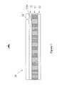
- FIG. 2depicts one embodiment of the front light system of the present invention which is on the top surface of a reflective display ( 10 ) as shown in FIG. 1 .
- the top surface (i.e., the side of electrode layer 12 ) of the reflective display ( 10 )is the viewing side.
- the term “a front light system”is intended to indicate a lighting system which is on the viewing side of a reflective display.
- FIG. 2is a cross-section view of the system.
- the systemis built on a substrate layer ( 21 ).
- the substrate layeris transparent and may be a rigid film or a flexible film.
- a flexible substratemay be formed from a material, such as PMMA, PET or the like.
- the thickness of the substrate layer ( 21 )is preferably in the range of 50 to 150 microns for a flexible display application; but may be thicker for a non-flexible display application.
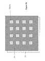
- the OLED light source ( 22 ) in the form of small dots ( 80 )is scattered throughout the surface of the substrate layer (see FIG. 8 ).
- the dotscan be of any shape and spacing, and their sizes are in the range of 5 to 50 microns, preferably in the range of 5 to 20 microns.
- Each of the light sourcesis sandwiched between two electrodes ( 23 and 24 ), one cathode and one anode.
- the electrodes ( 23 ) between the OLED light sources ( 22 ) and the substrate layer ( 21 )are transparent.
- the electrodes ( 24 ) on top of the OLED light sources ( 22 )may be transparent or non-transparent.
- the configurations of the electrodesmay vary and they are described in sections below.
- the cathode and anode electrodesenable driving of an OLED light source to emit light. The emitted light shines directly onto the reflective surface ( 11 a ) of the display film ( 11 ) of FIG. 1 and is then reflected and scattered by the reflective surface.
- the displayis viewed by an observer looking through the transparent substrate layer ( 21 ) in the areas where there are no OLED dots.
- the area of non-transparency due to the OLED structureis kept to a small fraction of the total area so that the viewing of the display is not obstructed.
- the total area of OLEDsmay be 20 ⁇ 20 microns in size and they are on a surface space of 250 ⁇ 250 microns. In this case, more than 99% of the display area is not covered by OLEDs (see FIG. 8 ).
- the OLED light sourcescan be printed onto, and appear as a thin film layer on, a surface.
- a reflective light shield film ( 25 )to block the light from directly reaching the observer, if the electrode ( 24 ) is transparent.
- the purpose of the light shieldis not only to block the light from directly shining into the observer's eyes, but also to reflect the upwardly emitted light back onto the display surface, hence achieving certain light gain.
- the light shield filmmay be formed from a material such as aluminum or silver.
- the electrode ( 24 )is non-transparent, the electrode may serve as a light shield layer. In this case, no additional light shield film is needed.
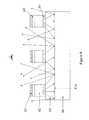
- FIG. 3 dprovides a top view of a design in which the cathode and anode electrodes are arranged in a column and row fashion.
- FIGS. 3 a - 3 dshow how such a front light system is built in sequence.
- FIG. 3 atwo cathode electrodes ( 33 ) on a transparent substrate layer ( 31 ) are shown as column electrodes.
- FIG. 3 bOLED light sources ( 32 ) are printed on the column electrodes ( 33 ).
- anode electrodes ( 34 ) in rowsare placed over the OLED light sources ( 32 ).
- the OLED light sourcesare slightly larger than the actual overlapping areas of the cathode and anode electrodes to avoid any direct contact between the two electrodes.
- a light shield film ( 35 )is on top of the anode electrodes to block the OLED light from directly shining into the eyes of a viewer.
- the electrode stripsare transparent, they usually are formed from ITO, a conducting polymer or other transparent conductive materials.
- the electrode stripsmay be applied by any of the conventional methods used to deposit a conductive material on a surface, such as patterned printing, shadow mask, sputtering, vapor deposition, vacuum deposition, electroplating, electro-less plating, electroforming or thin film deposition with photoresist patterning.
- All the column (cathode) electrodesare driven simultaneously at one potential and all the row (anode) electrodes are driven simultaneously at another potential, thus creating a voltage difference between the two electrodes to generate a current which flows through the OLED light material to cause all of the OLED light sources to emit light.
- the column electrodes ( 33 )are underneath the OLED light sources whereas the row electrodes ( 34 ) are above the OLED light sources. It is also possible to have the row electrodes ( 34 ) to be underneath the OLED light sources ( 32 ) and the column electrodes ( 33 ) to be above the OLED light sources. Either the cathode electrode or the anode electrode may be underneath the OLED light source and the other above the OLED light source. In any case, the electrodes between the transparent substrate layer ( 31 ) and the OLED light sources ( 32 ) are transparent.
- the electrode strips on top of the OLED light sourcesmay be non-transparent.
- the opaque electrode areais to be kept at a small fraction of the total surface area.
- the operation of the front light system with non-transparent electrodesis the same as that of FIG. 3 .
- FIG. 4is a top view of an alternative design.
- the electrodesare arranged in a co-linear fashion.
- the cathode electrodes ( 43 ) and anode electrodes ( 44 )are arranged in parallel.
- a conductive bridge ( 46 )contacts the cathode ( 43 ) and is then formed laterally to overlap the OLED ( 42 a ) which is on top of the anode ( 44 ). Since FIG. 4 is a top view, the OLED light source ( 42 a ) placed between the anode ( 44 ) and the conductive bridge ( 46 ) can not be seen.
- the voltage difference between the cathode and the anodegenerates a current which causes the OLED light source ( 42 a ) to emit light.
- Other OLED light sources(such as 42 b ) may be similarly configured.
- On top of each OLED light sourcethere is a light shield ( 45 ) if the electrode layer on top of the OLED light sources ( 42 a and 42 b ) is transparent.
- FIG. 5 aillustrates a further alternative design of the front light system, in a cross-section view.
- the cathode and anode electrodesare in the form of layers. In other words, the electrode layers are not patterned.
- the cathode electrode layer ( 53 )is on a transparent substrate layer ( 51 ).
- multiple OLED light sources ( 52 )are sandwiched between the cathode and anode electrode layers ( 53 and 54 ).
- An insulating layer ( 53 a )may be present between the cathode and anode layers to prevent direct contact between the two electrode layers where no OLED light sources are present.
- a light shield ( 55 )is on top of each OLED light source ( 52 ) if the electrode layer on top of the OLED light sources is transparent.
- FIG. 5 bis a top view of the front light system of FIG. 5 a.
- FIGS. 3-5only demonstrate a few examples of electrode configurations which may be implemented for the present invention. Many other comparable electrode configurations which are not specifically described may also be utilized and all of those are encompassed within the scope of the present invention.
- FIG. 6illustrates how a front light system of the present invention is integrated with a reflective display ( 60 ).
- the OLED light sources ( 62 ) formed on a transparent substrate layer ( 61 )are sandwiched between two electrodes ( 63 and 64 ).
- Light shields ( 65 ), if present,are also shown to be on top of the OLED light sources.
- the light emitted by the OLED light sourcesstrikes a reflective surface ( 61 a ) of the reflective display ( 60 ) through the transparent electrodes ( 64 ) and the transparent substrate layer ( 61 ) and is then reflected and scattered.
- the reflected and scattered lightbrightens the viewing surface of the display, thus facilitating viewing of the images displayed by the reflective display.
- the presence of the light shield film ( 65 ) for each light source ( 62 )blocks the light emitted from the light source from directly reaching the observer, creating a more uniform and soothing lighting condition.
- the front light system of the present inventionis suitable for all types of reflective displays.
- One of the examplesis demonstrated in FIGS. 7 a , 7 b and 7 c.
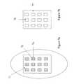
- FIG. 7 ais a top view of a keymat assembly which may be used in a device such as a cell phone.
- the keymat ( 71 )has keys ( 76 ) (or buttons) on its top surface.
- a reflective display ( 70 )is overlaid on the keys ( 76 ) and it can display visually viewable information, such as alphabets, numbers or operational commends. The areas between the keys may also be covered by a reflective display.
- FIG. 7 bis a top view of a front light film ( 77 ) of the present invention.
- the OLED light sourcesare embedded in the film except the transparent areas ( 78 ).
- the transparent areas ( 78 )correspond to the keys ( 76 ) on the keymat.
- the front light film ( 77 )is then placed over (e.g., laminated over) the keymat ( 71 ).
- the reflective displayproduces images to be shown on the keys and the images are visible through the transparent areas ( 78 ) of the front light film ( 77 ).
- the light generated by the OLED light sourcesshines sideways onto the keys and illuminates them when required.
- the LED materialmay be one uniform layer filling all of the areas on the front light film ( 77 ), except the transparent areas ( 78 ).
- FIG. 7 cis a cross-section view of a keymat assembly with a front light system of the invention.
- a reflective display ( 70 )is on top of the touch sensitive keys ( 76 ).
- a front light film ( 77 )is placed over the reflective display ( 70 ) with the transparent areas ( 78 ) corresponding to the keys ( 76 ) to allow the images displayed on the keys to be seen through the transparent areas ( 78 ).
- the front light filmas shown, has electrodes ( 73 & 74 ), OLED light sources ( 72 ) and light shield film ( 75 ), if present.
- the front light film ( 77 )may be formed using a shadow mask. While less preferably, the transparent areas on the front light film ( 77 ) may also be formed by creating openings on a complete sheet of front light film, using die punch, laser cutting or other similar methods.
Landscapes
- Engineering & Computer Science (AREA)
- Theoretical Computer Science (AREA)
- General Engineering & Computer Science (AREA)
- Computer Hardware Design (AREA)
- Human Computer Interaction (AREA)
- Physics & Mathematics (AREA)
- General Physics & Mathematics (AREA)
- Electroluminescent Light Sources (AREA)
Abstract
Description
Claims (6)
Priority Applications (1)
| Application Number | Priority Date | Filing Date | Title |
|---|---|---|---|
| US12/182,024US8743077B1 (en) | 2007-08-01 | 2008-07-29 | Front light system for reflective displays |
Applications Claiming Priority (2)
| Application Number | Priority Date | Filing Date | Title |
|---|---|---|---|
| US95341007P | 2007-08-01 | 2007-08-01 | |
| US12/182,024US8743077B1 (en) | 2007-08-01 | 2008-07-29 | Front light system for reflective displays |
Publications (1)
| Publication Number | Publication Date |
|---|---|
| US8743077B1true US8743077B1 (en) | 2014-06-03 |
Family
ID=50781272
Family Applications (1)
| Application Number | Title | Priority Date | Filing Date |
|---|---|---|---|
| US12/182,024Active2029-05-01US8743077B1 (en) | 2007-08-01 | 2008-07-29 | Front light system for reflective displays |
Country Status (1)
| Country | Link |
|---|---|
| US (1) | US8743077B1 (en) |
Cited By (27)
| Publication number | Priority date | Publication date | Assignee | Title |
|---|---|---|---|---|
| US20160013447A1 (en)* | 2012-02-10 | 2016-01-14 | Osram Opto Semiconductors Gmbh | Radiation-emitting device |
| CN106855763A (en)* | 2017-03-10 | 2017-06-16 | 武汉华星光电技术有限公司 | A kind of array base palte and self-tolerant embedded touch control display panel |
| US10317767B2 (en) | 2014-02-07 | 2019-06-11 | E Ink Corporation | Electro-optic display backplane structure with drive components and pixel electrodes on opposed surfaces |
| US10324577B2 (en) | 2017-02-28 | 2019-06-18 | E Ink Corporation | Writeable electrophoretic displays including sensing circuits and styli configured to interact with sensing circuits |
| US20190187848A1 (en)* | 2017-12-15 | 2019-06-20 | Boe Technology Group Co., Ltd. | Oled touch panel and method for manufacturing the same |
| CN110277423A (en)* | 2019-06-28 | 2019-09-24 | 京东方科技集团股份有限公司 | A method for manufacturing a display panel, as well as a display panel and a display device |
| US10466565B2 (en) | 2017-03-28 | 2019-11-05 | E Ink Corporation | Porous backplane for electro-optic display |
| US10495941B2 (en) | 2017-05-19 | 2019-12-03 | E Ink Corporation | Foldable electro-optic display including digitization and touch sensing |
| US10573257B2 (en) | 2017-05-30 | 2020-02-25 | E Ink Corporation | Electro-optic displays |
| WO2020097462A1 (en) | 2018-11-09 | 2020-05-14 | E Ink Corporation | Electro-optic displays |
| US10672221B2 (en)* | 2013-03-12 | 2020-06-02 | Tcs John Huxley Europe Limited | Gaming table |
| US10824042B1 (en) | 2017-10-27 | 2020-11-03 | E Ink Corporation | Electro-optic display and composite materials having low thermal sensitivity for use therein |
| US10882042B2 (en) | 2017-10-18 | 2021-01-05 | E Ink Corporation | Digital microfluidic devices including dual substrates with thin-film transistors and capacitive sensing |
| US11175561B1 (en) | 2018-04-12 | 2021-11-16 | E Ink Corporation | Electrophoretic display media with network electrodes and methods of making and using the same |
| WO2021247470A1 (en) | 2020-06-03 | 2021-12-09 | E Ink Corporation | Foldable electrophoretic display module including non-conductive support plate |
| US11314141B2 (en) | 2018-05-04 | 2022-04-26 | E Ink Holdings Inc. | Electrophoretic display device |
| US11353759B2 (en) | 2018-09-17 | 2022-06-07 | Nuclera Nucleics Ltd. | Backplanes with hexagonal and triangular electrodes |
| US11404013B2 (en) | 2017-05-30 | 2022-08-02 | E Ink Corporation | Electro-optic displays with resistors for discharging remnant charges |
| US11511096B2 (en) | 2018-10-15 | 2022-11-29 | E Ink Corporation | Digital microfluidic delivery device |
| US11521565B2 (en) | 2018-12-28 | 2022-12-06 | E Ink Corporation | Crosstalk reduction for electro-optic displays |
| US11537024B2 (en) | 2018-12-30 | 2022-12-27 | E Ink California, Llc | Electro-optic displays |
| WO2023167901A1 (en) | 2022-03-01 | 2023-09-07 | E Ink California, Llc | Temperature compensation in electro-optic displays |
| US11935495B2 (en) | 2021-08-18 | 2024-03-19 | E Ink Corporation | Methods for driving electro-optic displays |
| US12190730B2 (en) | 2022-02-28 | 2025-01-07 | E Ink Corporation | Parking space management system |
| US12313951B2 (en) | 2016-06-10 | 2025-05-27 | E Ink Corporation | Electro-optic display apparatus |
| WO2025147504A1 (en) | 2024-01-05 | 2025-07-10 | E Ink Corporation | An electrophoretic medium comprising particles having a pigment core and a polymeric shell |
| WO2025151355A1 (en) | 2024-01-08 | 2025-07-17 | E Ink Corporation | Electrophoretic device having an adhesive layer comprising conductive filler particles and a polymeric dispersant |
Citations (41)
| Publication number | Priority date | Publication date | Assignee | Title |
|---|---|---|---|---|
| US5796509A (en)* | 1996-08-21 | 1998-08-18 | International Business Machines Corporation | Thin film frontlighting and backlighting for spatial light modulators |
| US5847690A (en)* | 1995-10-24 | 1998-12-08 | Lucent Technologies Inc. | Integrated liquid crystal display and digitizer having a black matrix layer adapted for sensing screen touch location |
| US5930026A (en) | 1996-10-25 | 1999-07-27 | Massachusetts Institute Of Technology | Nonemissive displays and piezoelectric power supplies therefor |
| US5961804A (en) | 1997-03-18 | 1999-10-05 | Massachusetts Institute Of Technology | Microencapsulated electrophoretic display |
| US6013538A (en)* | 1997-11-24 | 2000-01-11 | The Trustees Of Princeton University | Method of fabricating and patterning OLEDs |
| US20010048379A1 (en)* | 2000-05-02 | 2001-12-06 | Terho Kaikuranta | Keypad illumination arrangement that enables dynamic and individual illumination of keys, and method of using the same |
| US20020130832A1 (en)* | 2001-03-13 | 2002-09-19 | Baucom Allan Scott | Apparatus for displaying drawings |
| US20030020084A1 (en)* | 1991-01-18 | 2003-01-30 | Kopin Corporation | Method of making light emitting diode displays |
| US20030121981A1 (en)* | 2001-12-28 | 2003-07-03 | Michael Slutsky | Lighthouse ASIC |
| US6704004B1 (en)* | 2000-08-17 | 2004-03-09 | Nokia Mobile Phones Ltd. | Arrangement for integration of key illumination into keymat of portable electronic devices |
| US20040141106A1 (en)* | 2002-07-08 | 2004-07-22 | Ivan Yang-En Wu | [reflective liquid crystal display] |
| US20040263045A1 (en)* | 2001-08-30 | 2004-12-30 | Smith Euan Christopher | Optoelectronic displays |
| US20040266515A1 (en)* | 2003-06-24 | 2004-12-30 | Michael Gauselmann | Gaming machine with reel strips having an organic light emitting diode display |
| US20050001541A1 (en)* | 2000-05-06 | 2005-01-06 | Semiconductor Energy Laboratory Co., Ltd., A Japan Corporation | Light-emitting device and electric apparatus |
| US20050073823A1 (en)* | 2003-08-08 | 2005-04-07 | Harry Engelmann | Operating surface, in particular for home appliances |
| US20050083592A1 (en)* | 2003-09-10 | 2005-04-21 | Yaakov Amitai | High Brightness optical device |
| US20050112403A1 (en)* | 2003-11-25 | 2005-05-26 | Sang-Hyun Ju | Full color organic electroluminescent device |
| US20050134189A1 (en)* | 2003-12-18 | 2005-06-23 | Semiconductor Energy Laboratory Co., Ltd. | Display device and manufacturing method thereof |
| US6930818B1 (en) | 2000-03-03 | 2005-08-16 | Sipix Imaging, Inc. | Electrophoretic display and novel process for its manufacture |
| US6947017B1 (en)* | 2001-08-29 | 2005-09-20 | Palm, Inc. | Dynamic brightness range for portable computer displays based on ambient conditions |
| US20050206828A1 (en)* | 2004-03-20 | 2005-09-22 | Sun-Youl Lee | Electroluminescent display device and method for manufacturing the same |
| US20060034065A1 (en)* | 2004-08-10 | 2006-02-16 | Innovalight, Inc. | Light strips for lighting and backlighting applications |
| US20060071233A1 (en)* | 2004-10-05 | 2006-04-06 | Sang-Hwan Cho | Organic light emitting device and method of manufacturing the same |
| US7102162B2 (en)* | 2002-12-12 | 2006-09-05 | Che-Kuei Mai | Plane light source structure for planar display |
| US20070152983A1 (en)* | 2005-12-30 | 2007-07-05 | Apple Computer, Inc. | Touch pad with symbols based on mode |
| US20070252818A1 (en)* | 2006-04-28 | 2007-11-01 | Joseph Zlotnicki | Method and apparatus for efficient data input |
| US20070257821A1 (en)* | 2006-04-20 | 2007-11-08 | Son Jae S | Reconfigurable tactile sensor input device |
| US7301273B2 (en)* | 2003-02-20 | 2007-11-27 | Barco Nv | Display element array for emissive, fixed format display |
| US20070279852A1 (en)* | 2004-02-27 | 2007-12-06 | Daniel Simon R | Wearable Modular Interface Strap |
| US20080234044A1 (en)* | 2007-03-21 | 2008-09-25 | Konami Gaming Incorporated | Gaming machine having touch panel switch |
| US20080259057A1 (en)* | 2005-09-14 | 2008-10-23 | Johannes Brons | Electronic Reading Device Mimicking a Reading experience of a Paper Document |
| US7514859B2 (en)* | 2004-12-20 | 2009-04-07 | Hewlett-Packard Development Company, L.P. | Ultraviolet emitter display apparatus |
| US20090134986A1 (en)* | 2007-11-26 | 2009-05-28 | Alan Joseph Bauer | In-transitcar alarm |
| US7629400B2 (en)* | 1999-06-11 | 2009-12-08 | Sydney Hyman | Image making medium |
| US7811170B2 (en)* | 2001-05-04 | 2010-10-12 | Igt | Light emitting interface displays for a gaming machine |
| US7830368B2 (en)* | 2006-06-06 | 2010-11-09 | 3M Innovative Properties Company | Keypad with virtual image |
| US7917034B2 (en)* | 2007-04-13 | 2011-03-29 | Motorola Mobility, Inc. | Synchronization and processing of secure information via optically transmitted data |
| US7924272B2 (en)* | 2006-11-27 | 2011-04-12 | Microsoft Corporation | Infrared sensor integrated in a touch panel |
| US8025434B2 (en)* | 2008-06-03 | 2011-09-27 | Nokia Corporation | Two-sided illumination device |
| US8130202B2 (en)* | 2007-05-01 | 2012-03-06 | International Business Machines Corporation | Infrared touch screen gated by touch force |
| US8477125B2 (en)* | 2005-12-21 | 2013-07-02 | Samsung Display Co., Ltd. | Photo sensor and organic light-emitting display using the same |
- 2008
- 2008-07-29USUS12/182,024patent/US8743077B1/enactiveActive
Patent Citations (41)
| Publication number | Priority date | Publication date | Assignee | Title |
|---|---|---|---|---|
| US20030020084A1 (en)* | 1991-01-18 | 2003-01-30 | Kopin Corporation | Method of making light emitting diode displays |
| US5847690A (en)* | 1995-10-24 | 1998-12-08 | Lucent Technologies Inc. | Integrated liquid crystal display and digitizer having a black matrix layer adapted for sensing screen touch location |
| US5796509A (en)* | 1996-08-21 | 1998-08-18 | International Business Machines Corporation | Thin film frontlighting and backlighting for spatial light modulators |
| US5930026A (en) | 1996-10-25 | 1999-07-27 | Massachusetts Institute Of Technology | Nonemissive displays and piezoelectric power supplies therefor |
| US5961804A (en) | 1997-03-18 | 1999-10-05 | Massachusetts Institute Of Technology | Microencapsulated electrophoretic display |
| US6013538A (en)* | 1997-11-24 | 2000-01-11 | The Trustees Of Princeton University | Method of fabricating and patterning OLEDs |
| US7629400B2 (en)* | 1999-06-11 | 2009-12-08 | Sydney Hyman | Image making medium |
| US6930818B1 (en) | 2000-03-03 | 2005-08-16 | Sipix Imaging, Inc. | Electrophoretic display and novel process for its manufacture |
| US20010048379A1 (en)* | 2000-05-02 | 2001-12-06 | Terho Kaikuranta | Keypad illumination arrangement that enables dynamic and individual illumination of keys, and method of using the same |
| US20050001541A1 (en)* | 2000-05-06 | 2005-01-06 | Semiconductor Energy Laboratory Co., Ltd., A Japan Corporation | Light-emitting device and electric apparatus |
| US6704004B1 (en)* | 2000-08-17 | 2004-03-09 | Nokia Mobile Phones Ltd. | Arrangement for integration of key illumination into keymat of portable electronic devices |
| US20020130832A1 (en)* | 2001-03-13 | 2002-09-19 | Baucom Allan Scott | Apparatus for displaying drawings |
| US7811170B2 (en)* | 2001-05-04 | 2010-10-12 | Igt | Light emitting interface displays for a gaming machine |
| US6947017B1 (en)* | 2001-08-29 | 2005-09-20 | Palm, Inc. | Dynamic brightness range for portable computer displays based on ambient conditions |
| US20040263045A1 (en)* | 2001-08-30 | 2004-12-30 | Smith Euan Christopher | Optoelectronic displays |
| US20030121981A1 (en)* | 2001-12-28 | 2003-07-03 | Michael Slutsky | Lighthouse ASIC |
| US20040141106A1 (en)* | 2002-07-08 | 2004-07-22 | Ivan Yang-En Wu | [reflective liquid crystal display] |
| US7102162B2 (en)* | 2002-12-12 | 2006-09-05 | Che-Kuei Mai | Plane light source structure for planar display |
| US7301273B2 (en)* | 2003-02-20 | 2007-11-27 | Barco Nv | Display element array for emissive, fixed format display |
| US20040266515A1 (en)* | 2003-06-24 | 2004-12-30 | Michael Gauselmann | Gaming machine with reel strips having an organic light emitting diode display |
| US20050073823A1 (en)* | 2003-08-08 | 2005-04-07 | Harry Engelmann | Operating surface, in particular for home appliances |
| US20050083592A1 (en)* | 2003-09-10 | 2005-04-21 | Yaakov Amitai | High Brightness optical device |
| US20050112403A1 (en)* | 2003-11-25 | 2005-05-26 | Sang-Hyun Ju | Full color organic electroluminescent device |
| US20050134189A1 (en)* | 2003-12-18 | 2005-06-23 | Semiconductor Energy Laboratory Co., Ltd. | Display device and manufacturing method thereof |
| US20070279852A1 (en)* | 2004-02-27 | 2007-12-06 | Daniel Simon R | Wearable Modular Interface Strap |
| US20050206828A1 (en)* | 2004-03-20 | 2005-09-22 | Sun-Youl Lee | Electroluminescent display device and method for manufacturing the same |
| US20060034065A1 (en)* | 2004-08-10 | 2006-02-16 | Innovalight, Inc. | Light strips for lighting and backlighting applications |
| US20060071233A1 (en)* | 2004-10-05 | 2006-04-06 | Sang-Hwan Cho | Organic light emitting device and method of manufacturing the same |
| US7514859B2 (en)* | 2004-12-20 | 2009-04-07 | Hewlett-Packard Development Company, L.P. | Ultraviolet emitter display apparatus |
| US20080259057A1 (en)* | 2005-09-14 | 2008-10-23 | Johannes Brons | Electronic Reading Device Mimicking a Reading experience of a Paper Document |
| US8477125B2 (en)* | 2005-12-21 | 2013-07-02 | Samsung Display Co., Ltd. | Photo sensor and organic light-emitting display using the same |
| US20070152983A1 (en)* | 2005-12-30 | 2007-07-05 | Apple Computer, Inc. | Touch pad with symbols based on mode |
| US20070257821A1 (en)* | 2006-04-20 | 2007-11-08 | Son Jae S | Reconfigurable tactile sensor input device |
| US20070252818A1 (en)* | 2006-04-28 | 2007-11-01 | Joseph Zlotnicki | Method and apparatus for efficient data input |
| US7830368B2 (en)* | 2006-06-06 | 2010-11-09 | 3M Innovative Properties Company | Keypad with virtual image |
| US7924272B2 (en)* | 2006-11-27 | 2011-04-12 | Microsoft Corporation | Infrared sensor integrated in a touch panel |
| US20080234044A1 (en)* | 2007-03-21 | 2008-09-25 | Konami Gaming Incorporated | Gaming machine having touch panel switch |
| US7917034B2 (en)* | 2007-04-13 | 2011-03-29 | Motorola Mobility, Inc. | Synchronization and processing of secure information via optically transmitted data |
| US8130202B2 (en)* | 2007-05-01 | 2012-03-06 | International Business Machines Corporation | Infrared touch screen gated by touch force |
| US20090134986A1 (en)* | 2007-11-26 | 2009-05-28 | Alan Joseph Bauer | In-transitcar alarm |
| US8025434B2 (en)* | 2008-06-03 | 2011-09-27 | Nokia Corporation | Two-sided illumination device |
Cited By (42)
| Publication number | Priority date | Publication date | Assignee | Title |
|---|---|---|---|---|
| US9728750B2 (en)* | 2012-02-10 | 2017-08-08 | Osram Oled Gmbh | Radiation-emitting device |
| US20160013447A1 (en)* | 2012-02-10 | 2016-01-14 | Osram Opto Semiconductors Gmbh | Radiation-emitting device |
| US11049361B2 (en)* | 2013-03-12 | 2021-06-29 | Tcs John Huxley Europe Limited | Gaming table |
| US10672221B2 (en)* | 2013-03-12 | 2020-06-02 | Tcs John Huxley Europe Limited | Gaming table |
| US10317767B2 (en) | 2014-02-07 | 2019-06-11 | E Ink Corporation | Electro-optic display backplane structure with drive components and pixel electrodes on opposed surfaces |
| US12313951B2 (en) | 2016-06-10 | 2025-05-27 | E Ink Corporation | Electro-optic display apparatus |
| US10324577B2 (en) | 2017-02-28 | 2019-06-18 | E Ink Corporation | Writeable electrophoretic displays including sensing circuits and styli configured to interact with sensing circuits |
| CN106855763A (en)* | 2017-03-10 | 2017-06-16 | 武汉华星光电技术有限公司 | A kind of array base palte and self-tolerant embedded touch control display panel |
| US10466565B2 (en) | 2017-03-28 | 2019-11-05 | E Ink Corporation | Porous backplane for electro-optic display |
| US11016358B2 (en) | 2017-03-28 | 2021-05-25 | E Ink Corporation | Porous backplane for electro-optic display |
| US10495941B2 (en) | 2017-05-19 | 2019-12-03 | E Ink Corporation | Foldable electro-optic display including digitization and touch sensing |
| US10573257B2 (en) | 2017-05-30 | 2020-02-25 | E Ink Corporation | Electro-optic displays |
| US11404013B2 (en) | 2017-05-30 | 2022-08-02 | E Ink Corporation | Electro-optic displays with resistors for discharging remnant charges |
| US10825405B2 (en) | 2017-05-30 | 2020-11-03 | E Ink Corporatior | Electro-optic displays |
| US11107425B2 (en) | 2017-05-30 | 2021-08-31 | E Ink Corporation | Electro-optic displays with resistors for discharging remnant charges |
| US10882042B2 (en) | 2017-10-18 | 2021-01-05 | E Ink Corporation | Digital microfluidic devices including dual substrates with thin-film transistors and capacitive sensing |
| US10824042B1 (en) | 2017-10-27 | 2020-11-03 | E Ink Corporation | Electro-optic display and composite materials having low thermal sensitivity for use therein |
| US10579177B2 (en)* | 2017-12-15 | 2020-03-03 | Boe Technology Group Co., Ltd. | OLED touch panel with reduced thickness and method for manufacturing the same |
| US20190187848A1 (en)* | 2017-12-15 | 2019-06-20 | Boe Technology Group Co., Ltd. | Oled touch panel and method for manufacturing the same |
| US11175561B1 (en) | 2018-04-12 | 2021-11-16 | E Ink Corporation | Electrophoretic display media with network electrodes and methods of making and using the same |
| US11656524B2 (en) | 2018-04-12 | 2023-05-23 | E Ink Corporation | Electrophoretic display media with network electrodes and methods of making and using the same |
| US11314141B2 (en) | 2018-05-04 | 2022-04-26 | E Ink Holdings Inc. | Electrophoretic display device |
| US11353759B2 (en) | 2018-09-17 | 2022-06-07 | Nuclera Nucleics Ltd. | Backplanes with hexagonal and triangular electrodes |
| US11511096B2 (en) | 2018-10-15 | 2022-11-29 | E Ink Corporation | Digital microfluidic delivery device |
| US12186514B2 (en) | 2018-10-15 | 2025-01-07 | E Ink Corporation | Digital microfluidic delivery device |
| US11450287B2 (en) | 2018-11-09 | 2022-09-20 | E Ink Corporation | Electro-optic displays |
| WO2020097462A1 (en) | 2018-11-09 | 2020-05-14 | E Ink Corporation | Electro-optic displays |
| US11145262B2 (en) | 2018-11-09 | 2021-10-12 | E Ink Corporation | Electro-optic displays |
| US11521565B2 (en) | 2018-12-28 | 2022-12-06 | E Ink Corporation | Crosstalk reduction for electro-optic displays |
| US12032264B2 (en) | 2018-12-30 | 2024-07-09 | E Ink Corporation | Electro-optic displays |
| US12339560B2 (en) | 2018-12-30 | 2025-06-24 | E Ink Corporation | Electro-optic displays |
| US11537024B2 (en) | 2018-12-30 | 2022-12-27 | E Ink California, Llc | Electro-optic displays |
| CN110277423A (en)* | 2019-06-28 | 2019-09-24 | 京东方科技集团股份有限公司 | A method for manufacturing a display panel, as well as a display panel and a display device |
| US11874580B2 (en) | 2020-06-03 | 2024-01-16 | E Ink Corporation | Foldable electrophoretic display module including non-conductive support plate |
| WO2021247470A1 (en) | 2020-06-03 | 2021-12-09 | E Ink Corporation | Foldable electrophoretic display module including non-conductive support plate |
| US11513415B2 (en) | 2020-06-03 | 2022-11-29 | E Ink Corporation | Foldable electrophoretic display module including non-conductive support plate |
| US11935495B2 (en) | 2021-08-18 | 2024-03-19 | E Ink Corporation | Methods for driving electro-optic displays |
| US12190730B2 (en) | 2022-02-28 | 2025-01-07 | E Ink Corporation | Parking space management system |
| US11830449B2 (en) | 2022-03-01 | 2023-11-28 | E Ink Corporation | Electro-optic displays |
| WO2023167901A1 (en) | 2022-03-01 | 2023-09-07 | E Ink California, Llc | Temperature compensation in electro-optic displays |
| WO2025147504A1 (en) | 2024-01-05 | 2025-07-10 | E Ink Corporation | An electrophoretic medium comprising particles having a pigment core and a polymeric shell |
| WO2025151355A1 (en) | 2024-01-08 | 2025-07-17 | E Ink Corporation | Electrophoretic device having an adhesive layer comprising conductive filler particles and a polymeric dispersant |
Similar Documents
| Publication | Publication Date | Title |
|---|---|---|
| US8743077B1 (en) | Front light system for reflective displays | |
| US8022615B2 (en) | Light generating layer for a reflective display | |
| US9614014B2 (en) | Display device | |
| TWI259023B (en) | Light emitting device, its manufacturing method, and electronic equipment | |
| US8164820B2 (en) | Display device | |
| KR20160032099A (en) | Data processing device | |
| CN102548078B (en) | Lighting device, its manufacture method and electronic equipment | |
| US20060290623A1 (en) | Light emitting device using organic electroluminescent element | |
| KR20160033106A (en) | Data processing device | |
| JP2005502086A5 (en) | ||
| CN101373576B (en) | Image display system | |
| CN100511700C (en) | Emissive device and electronic apparatus | |
| CN108364990A (en) | Double face display panel and double-side display device | |
| EP1760801A2 (en) | Using prismatic microstructured films for image blending in OLEDS | |
| US8698978B2 (en) | Electroluminescent displays | |
| JP2005332616A (en) | Organic electroluminescence display device and electronic apparatus | |
| US6809709B2 (en) | Organic electro-luminescence device | |
| JP5228268B2 (en) | Organic electroluminescence element and liquid crystal display device | |
| US20090045751A1 (en) | Systems for displaying images | |
| US8076843B2 (en) | Organic electroluminescence display device | |
| US20200075681A1 (en) | Transparent display panel, fabricating method for the same, and display device | |
| US7397181B2 (en) | Image display panel consisting of a matrix of memory-effect electroluminescent cells | |
| KR20060129974A (en) | Liquid crystal display device and electronic device provided with the liquid crystal display device | |
| KR100826582B1 (en) | Backlight Unit of LCD | |
| JP2012142094A (en) | Lighting device, manufacturing method thereof and electronic apparatus |
Legal Events
| Date | Code | Title | Description |
|---|---|---|---|
| AS | Assignment | Owner name:SIPIX IMAGING, INC., CALIFORNIA Free format text:ASSIGNMENT OF ASSIGNORS INTEREST;ASSIGNOR:SPRAGUE, ROBERT A.;REEL/FRAME:021550/0159 Effective date:20080819 | |
| STCF | Information on status: patent grant | Free format text:PATENTED CASE | |
| AS | Assignment | Owner name:E INK CALIFORNIA, LLC, CALIFORNIA Free format text:CHANGE OF NAME;ASSIGNOR:SIPIX IMAGING, INC.;REEL/FRAME:033280/0408 Effective date:20140701 | |
| MAFP | Maintenance fee payment | Free format text:PAYMENT OF MAINTENANCE FEE, 4TH YEAR, LARGE ENTITY (ORIGINAL EVENT CODE: M1551) Year of fee payment:4 | |
| MAFP | Maintenance fee payment | Free format text:PAYMENT OF MAINTENANCE FEE, 8TH YEAR, LARGE ENTITY (ORIGINAL EVENT CODE: M1552); ENTITY STATUS OF PATENT OWNER: LARGE ENTITY Year of fee payment:8 | |
| AS | Assignment | Owner name:E INK CORPORATION, MASSACHUSETTS Free format text:ASSIGNMENT OF ASSIGNORS INTEREST;ASSIGNOR:E INK CALIFORNIA, LLC;REEL/FRAME:065154/0965 Effective date:20230925 |