US8741778B2 - Uniform dry etch in two stages - Google Patents
Uniform dry etch in two stagesDownload PDFInfo
- Publication number
- US8741778B2 US8741778B2US13/197,487US201113197487AUS8741778B2US 8741778 B2US8741778 B2US 8741778B2US 201113197487 AUS201113197487 AUS 201113197487AUS 8741778 B2US8741778 B2US 8741778B2
- Authority
- US
- United States
- Prior art keywords
- etch
- dry
- silicon oxide
- stage
- etch rate
- Prior art date
- Legal status (The legal status is an assumption and is not a legal conclusion. Google has not performed a legal analysis and makes no representation as to the accuracy of the status listed.)
- Active, expires
Links
Images


Classifications
- H—ELECTRICITY
- H01—ELECTRIC ELEMENTS
- H01L—SEMICONDUCTOR DEVICES NOT COVERED BY CLASS H10
- H01L21/00—Processes or apparatus adapted for the manufacture or treatment of semiconductor or solid state devices or of parts thereof
- H01L21/02—Manufacture or treatment of semiconductor devices or of parts thereof
- H01L21/04—Manufacture or treatment of semiconductor devices or of parts thereof the devices having potential barriers, e.g. a PN junction, depletion layer or carrier concentration layer
- H01L21/18—Manufacture or treatment of semiconductor devices or of parts thereof the devices having potential barriers, e.g. a PN junction, depletion layer or carrier concentration layer the devices having semiconductor bodies comprising elements of Group IV of the Periodic Table or AIIIBV compounds with or without impurities, e.g. doping materials
- H01L21/30—Treatment of semiconductor bodies using processes or apparatus not provided for in groups H01L21/20 - H01L21/26
- H01L21/302—Treatment of semiconductor bodies using processes or apparatus not provided for in groups H01L21/20 - H01L21/26 to change their surface-physical characteristics or shape, e.g. etching, polishing, cutting
- H01L21/306—Chemical or electrical treatment, e.g. electrolytic etching
- H01L21/3065—Plasma etching; Reactive-ion etching
- H—ELECTRICITY
- H01—ELECTRIC ELEMENTS
- H01L—SEMICONDUCTOR DEVICES NOT COVERED BY CLASS H10
- H01L21/00—Processes or apparatus adapted for the manufacture or treatment of semiconductor or solid state devices or of parts thereof
- H01L21/02—Manufacture or treatment of semiconductor devices or of parts thereof
- H01L21/04—Manufacture or treatment of semiconductor devices or of parts thereof the devices having potential barriers, e.g. a PN junction, depletion layer or carrier concentration layer
- H01L21/18—Manufacture or treatment of semiconductor devices or of parts thereof the devices having potential barriers, e.g. a PN junction, depletion layer or carrier concentration layer the devices having semiconductor bodies comprising elements of Group IV of the Periodic Table or AIIIBV compounds with or without impurities, e.g. doping materials
- H01L21/30—Treatment of semiconductor bodies using processes or apparatus not provided for in groups H01L21/20 - H01L21/26
- H01L21/31—Treatment of semiconductor bodies using processes or apparatus not provided for in groups H01L21/20 - H01L21/26 to form insulating layers thereon, e.g. for masking or by using photolithographic techniques; After treatment of these layers; Selection of materials for these layers
- H01L21/3105—After-treatment
- H01L21/311—Etching the insulating layers by chemical or physical means
- H01L21/31105—Etching inorganic layers
- H01L21/31111—Etching inorganic layers by chemical means
- H01L21/31116—Etching inorganic layers by chemical means by dry-etching
Definitions
- Integrated circuitsare made possible by processes which produce intricately patterned material layers on substrate surfaces. Producing patterned material on a substrate requires controlled methods for removal of exposed material. Chemical etching is used for a variety of purposes including transferring a pattern in photoresist into underlying layers, thinning layers or thinning lateral dimensions of features already present on the surface. Often it is desirable to have an etch process which etches one material faster than another helping e.g. a pattern transfer process proceed. Such an etch process is said to be selective to the first material. As a result of the diversity of materials, circuits and processes, etch processes have been developed with a selectivity towards a variety of materials.
- a SiconiTM etchis a remote plasma assisted dry etch process which involves the simultaneous exposure of a substrate to H 2 , NF 3 and NH 3 plasma by-products. Remote plasma excitation of the hydrogen and fluorine species allows plasma-damage-free substrate processing.
- the SiconiTM etchis largely conformal and selective towards silicon oxide layers but does not readily etch silicon regardless of whether the silicon is amorphous, crystalline or polycrystalline. The selectivity provides advantages for applications such as shallow trench isolation (STI) and inter-layer dielectric (ILD) recess formation.
- STIshallow trench isolation
- ILDinter-layer dielectric
- FIGS. 1-2show a flowchart of dry etch processing steps and associated schematic side-views of silicon oxide trimmed from trenches on a patterned substrate.
- the processbegins when a patterned substrate is transferred into the processing region (operation 110 ).
- the silicon oxide selective dry etchbegins (operation 120 ) when plasma by-products are delivered to the processing region.
- the selective dry etchresults in the consumption of silicon oxide 150 - 1 from within the trenches and the associated production of solid residue 155 above the remaining silicon oxide 150 - 2 .
- the SiconiTM processproduces solid by-products 155 which grow on the surface of the substrate as substrate material is removed.
- the solid by-productsare subsequently removed via sublimation (operation 130 ) when the temperature of the substrate is raised. Silicon oxide surface roughness and inter-trench etch rate variability may be observed following sublimation.
- a method of etching silicon oxide from a multiple trencheswhich allows more homogeneous etch rates among trenches.
- the surfaces of the etched silicon oxide within the trench following the etchmay also be smoother.
- the methodincludes two dry etch stages followed by a sublimation step.
- the first dry etch stageremoves silicon oxide quickly and produces large solid residue granules.
- the second dry etch stageremove silicon oxide slowly and produces small solid residue granules in amongst the large solid residue granules. Both the small and large solid residue are removed in the ensuing sublimation step. There is no sublimation step between the two dry etch stages.
- Embodiments of the inventioninclude methods of etching silicon oxide from multiple trenches on a surface of a patterned substrate in a substrate processing region of a substrate processing chamber.
- the methodsinclude the sequential steps of (1) dry etching the silicon oxide in each of the multiple trenches in a first dry-etch stage to form first solid by-products on the surface of a remaining silicon oxide in the multiple trenches, (2) dry etching the silicon oxide in each of the multiple trenches in a second dry-etch stage to form second solid by-products on the surface of a remaining silicon oxide in the multiple trenches, and (3) sublimating the first and second solid by-products from the multiple trenches.
- the silicon oxideis removed at a first etch rate during the first dry-etch stage.
- a second etch rate of the silicon oxide during the second dry-etch stageis less than the first etch rate.
- FIGS. 1A-1Dare a flowchart of dry etch processing steps and associated schematic side-views of silicon oxide trimmed from trenches on a patterned substrate.
- FIG. 2is a flow chart of a dry etch process according to disclosed embodiments.
- FIGS. 3A-3Ddepict schematic side-views of silicon oxide trimmed from trenches on a patterned substrate according to disclosed embodiments.
- FIG. 4is a cross-sectional view of a processing chamber for performing etch processes according to disclosed embodiments.
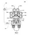
- FIG. 5is a processing system for performing etch processes according to disclosed embodiments.
- a method of etching silicon oxide from a multiple trencheswhich allows more homogeneous etch rates among trenches.
- the surfaces of the etched silicon oxide within the trench following the etchmay also be smoother.
- the methodincludes two dry etch stages followed by a sublimation step.
- the first dry etch stageremoves silicon oxide quickly and produces large solid residue granules.
- the second dry etch stageremove silicon oxide slowly and produces small solid residue granules in amongst the large solid residue granules. Both the small and large solid residue are removed in the ensuing sublimation step. There is no sublimation step between the two dry etch stages.
- SiconiTM etch processesare an example of a dry etch process and have used a hydrogen source such as ammonia (NH 3 ) in combination with a fluorine source such as nitrogen trifluoride (NF 3 ).
- a hydrogen sourcesuch as ammonia (NH 3 )
- a fluorine sourcesuch as nitrogen trifluoride (NF 3 ).
- the combinationflows into a remote plasma system (RPS) and the plasma effluents created therein are flowed into a substrate processing region.
- the effluentsreact with exposed silicon oxide to form solid residue which is then sublimated from the surface to complete the etch process.
- a thickness variationmay be observed across a silicon oxide surface treated with such a dry etch.
- the thickness variationmay manifest itself as a roughness across a blanket film, a wide trench or even the silicon surface within a narrow trench.
- Another manifestation of the thickness variationmay be observed as a etch rate variation among relatively narrow trenches.
- Silicon oxide gapfillmay be etched at
- the first dry-etch stageis similar to prior art SiconiTM processes.
- the solid by-products formed during the first stageare relatively large and expose varying surface areas between similarly sized narrow trenches in disclosed embodiments.
- the second dry-etch stageetches silicon oxide at a slower rate.
- the etchants of the second dry-etch stagecan diffuse through pores of the relatively large solid by-products and react with the varying exposed surface areas of silicon oxide underlying the large solid by-products.
- the second dry-etch stagesproduces relatively small solid by-products in amongst the large by-products.
- the quantity of small solid by-products, by weight,may be larger within trenches having a smaller quantity of large solid by-products.
- the consumption of silicon oxidei.e. the overall etch rate of the silicon oxide
- the trench-to-trench uniformityis therefore improved by combining two dry-etch stages in sequence without a sublimation step in between. A sublimation step is performed after the two dry-etch stages to remove both the large and small solid by-products.
- FIGS. 2 and 3 A- 3 Dare a flow chart of a dry etch process applied to a patterned substrate and depictions of the patterned substrate during the process, respectively, according to disclosed embodiments.
- the processbegins when a patterned substrate having silicon oxide gapfill 350 - 1 in multiple trenches is transferred into a processing chamber (operation 210 , FIG. 3A ). Flows of ammonia and nitrogen trifluoride are initiated into a plasma region separate from the processing region.
- the separate plasma regionmay be referred to as a remote plasma region herein and may be a distinct module from the processing chamber or a compartment within the processing chamber separated from the substrate processing region by a showerhead. Plasma effluents created in the remote plasma region travel into the substrate processing region to interact with the patterned substrate to remove silicon oxide.
- the interaction of the plasma effluents and the silicon oxideis separated into two phases.
- process parametersare selected to quickly remove the silicon oxide gapfill material (operation 220 ) leaving first solid residue granules 355 as shown in FIG. 3B .
- the process parametersare adjusted to begin the second phase of the dry etch.
- silicon oxide gapfillis removed at a slower rate (operation 240 ) and produces second solid residue granules 360 in amongst the first solid residue granules 355 over silicon oxide gapfill 350 - 3 as shown in FIG. 3C .
- the etch ratecharacterizes the silicon oxide removed.
- the etch interfaceis under the solid residue 355 , 360 . It is not necessary to remove the solid residue to gauge the etch rate, but it becomes easier to see the interface after the sublimation of the solid residue.
- the temperature of the silicon oxide during the interaction with the plasma effluentsmay be below one of 60° C., 50° C., 40° C. or 35° C., in different embodiments.
- the substrateis heated to sublimate the solid by-products (operation 250 ) and a schematic of the result is shown in FIG. 3D .
- the first solid residue granules 355 and the second solid residue granules 360are both removed by the sublimation process.
- the temperature of the solid residue and the silicon oxidemay be raised above one of 90° C., 100° C., 120° C. or 140° C. during the full sublimation, in different embodiments.
- the duration of the sublimationmay be above one of 45 seconds, 60 seconds, 75 seconds, 90 seconds or 120 seconds, in different embodiments.
- the width of the trenchesmay be less than one of 35 nm, 30 nm, 25 nm, 20 nm or 15 nm, in disclosed embodiments.
- the dry etch rate during the first dry-etch stageis greater than the dry etch rate during the second dry-etch stage.
- the etch rate of silicon oxide during the first dry-etch stagemay be greater than (or about) the etch rate during the second dry-etch stage by at least multiplicative factor of about 2, 3 or 5 in disclosed embodiments of the invention.
- the etch rate of silicon oxide during the first dry-etch stagemay also be less than (or about) the etch rate during the second dry-etch stage by a multiplicative factor of about 10 or 5 in embodiments. These upper limits may be combined with the lower limits to form additional embodiments.
- the etch rate during the first dry-etch stagemay be between one and about five times the etch rate during the second dry-etch stage.
- the first dry-etch stagemay last greater than or about 15 seconds or about 30 seconds, in embodiments.
- the first dry-etch stagemay last less than or about 2 minutes or about 1 minute, in embodiments.
- the second dry-etch stagemay last less than or about 30 seconds, 20 seconds or 10 seconds in embodiments of the invention.
- the second dry-etch stagemay last longer than or about 3 seconds, 5 seconds or 10 seconds. Any of the upper limits may be combined with any of the lower limits to provide additional ranges present in additional disclosed embodiments.
- the first solid by-productsare not sublimated between the first dry-etch stage and second dry-etch stage. Little or essentially no delay is present between the first dry-etch stage and the second dry-etch stage. In other embodiments, there is a pause between the two sets of process conditions during which etchants and other process effluents are removed from the substrate processing region.
- a variety of precursorsmay be used to create plasma effluents as described herein.
- a fluorine-containing precursormay be combined with a hydrogen-containing precursor in the remote plasma region to form the plasma effluents used for the etch processes.
- the fluorine-containing precursormay include one or more of nitrogen trifluoride, hydrogen fluoride, diatomic fluorine, monatomic fluorine and fluorine-substituted hydrocarbons.
- the hydrogen-containing precursormay include one or more of atomic hydrogen, molecular hydrogen, ammonia, a hydrocarbon and an incompletely halogen-substituted hydrocarbon.
- the etch rateis a complex function of the process parameters.
- fast and slow dry etch processes(during the first and second dry-etch stages, respectively) have been determined.
- Fast dry etch process during first dry-etch stagesare characterized by a faster saturation, i.e. a shorter time before the etch becomes self-limiting.
- the first dry-etch stagemay become self-limiting in about 30 seconds, for example, whereas the second dry-etch stage may become self-limiting in a couple minutes.
- the delayed saturationis indicative of an enhanced ability to diffuse past solid residue already created.
- the etching process of the first dry-etch stage (step 220 )would become self-limiting in one minute or less, while the etching process of the second dry-etch stage (step 230 ) would not become self-limiting until at least two minutes.
- the etching process of the first dry-etch stage (step 220 )would become self-limiting in 15-45 seconds, while the etching process of the second dry-etch stage (step 230 ) would not become self-limiting until at least three minutes.
- a first dry-etch stagemay involve a 2:1 ratio of NH 3 :NF 3 whereas a second dry-etch stage may involve a 10:1 ratio of NH 3 :NF 3 delivered to the remote plasma region to produce the plasma effluents.
- Thisis just an illustrative example of one method of achieving the fast and slow dry etches. Decreasing plasma power by 30% or 50%, in embodiments, from the first dry-etch stage to the second dry-etch stage has also been found to sufficiently reduce dry etch rates with only a small adjustment of the flow ratio (1:1 NH 3 :NF 3 ). It is anticipated that there are even more ways achieve fast and slow dry etch processes given the interdependence of the process parameters.
- FIG. 4is a partial cross sectional view showing an illustrative processing chamber 400 , in which, embodiments of the invention may be carried out.
- a hydrogen-containing precursor and a fluorine-containing precursormay be introduced through one or more apertures 451 into remote plasma region(s) 461 - 463 and excited by plasma power source 446 .
- the processing chamber 400includes a chamber body 412 , a lid assembly 402 , and a support assembly 410 .
- the lid assembly 402is disposed at an upper end of the chamber body 412
- the support assembly 410is at least partially disposed within the chamber body 412 .
- the processing chamber 400 and the associated hardwareare preferably formed from one or more process-compatible materials (e.g. aluminum, stainless steel, etc.).
- the chamber body 412includes a slit valve opening 460 formed in a sidewall thereof to provide access to the interior of the processing chamber 400 .
- the slit valve opening 460is selectively opened and closed to allow access to the interior of the chamber body 412 by a wafer handling robot (not shown).
- a wafercan be transported in and out of the processing chamber 400 through the slit valve opening 460 to an adjacent transfer chamber and/or load-lock chamber, or another chamber within a cluster tool.
- An exemplary cluster toolwhich may include processing chamber 400 is shown in FIG. 7 .
- chamber body 412includes a chamber body channel 413 for flowing a heat transfer fluid through chamber body 412 .
- the heat transfer fluidcan be a heating fluid or a coolant and is used to control the temperature of chamber body 412 during processing and substrate transfer. Heating the chamber body 412 may help to prevent unwanted condensation of the gas or byproducts on the chamber walls.
- Exemplary heat transfer fluidsinclude water, ethylene glycol, or a mixture thereof.
- An exemplary heat transfer fluidmay also include nitrogen gas.
- Support assembly 410may have a support assembly channel 404 for flowing a heat transfer fluid through support assembly 410 thereby affecting the substrate temperature.
- the chamber body 412can further include a liner 433 that surrounds the support assembly 410 .
- the liner 433is preferably removable for servicing and cleaning.
- the liner 433can be made of a metal such as aluminum, or a ceramic material. However, the liner 433 can be any process compatible material.
- the liner 433can be bead blasted to increase the adhesion of any material deposited thereon, thereby preventing flaking of material which results in contamination of the processing chamber 400 .
- the liner 433includes one or more apertures 435 and a pumping channel 429 formed therein that is in fluid communication with a vacuum system. The apertures 435 provide a flow path for gases into the pumping channel 429 , which provides an egress for the gases within the processing chamber 400 .
- the vacuum systemcan include a vacuum pump 425 and a throttle valve 427 to regulate flow of gases through the processing chamber 400 .
- the vacuum pump 425is coupled to a vacuum port 431 disposed on the chamber body 412 and therefore, in fluid communication with the pumping channel 429 formed within the liner 433 .
- gasesand “gases” are used interchangeably, unless otherwise noted, and refer to one or more reactants, catalysts, carrier, purge, cleaning, combinations thereof, as well as any other fluid introduced into the chamber body 412 .
- precursoris used to refer to any process gas which takes part in a reaction to either remove or deposit material from a surface.
- Apertures 435allow the pumping channel 429 to be in fluid communication with a processing region 440 within the chamber body 412 .
- the processing region 440is defined by a lower surface of the lid assembly 402 and an upper surface of the support assembly 410 , and is surrounded by the liner 433 .
- the apertures 435may be uniformly sized and evenly spaced about the liner 433 . However, any number, position, size or shape of apertures may be used, and each of those design parameters can vary depending on the desired flow pattern of gas across the substrate receiving surface as is discussed in more detail below. In addition, the size, number and position of the apertures 435 are configured to achieve uniform flow of gases exiting the processing chamber 400 .
- the aperture size and locationmay be configured to provide rapid or high capacity pumping to facilitate a rapid exhaust of gas from the chamber 400 .
- the number and size of apertures 435 in close proximity to the vacuum port 431may be smaller than the size of apertures 435 positioned farther away from the vacuum port 431 .
- a gas supply panel(not shown) is typically used to provide process gas(es) to the processing chamber 400 through one or more apertures 451 .
- the particular gas or gases that are useddepend upon the process or processes to be performed within the chamber 400 .
- Illustrative gasescan include, but are not limited to one or more precursors, reductants, catalysts, carriers, purge, cleaning, or any mixture or combination thereof.
- the one or more gases introduced to the processing chamber 400flow into plasma volume 461 through aperture(s) 451 in top plate 450 .
- processing gasesmay be introduced more directly through aperture(s) 452 into processing region 440 .
- Aperture(s) 452bypass the remote plasma excitation and are useful for processes involving gases that do not require plasma excitation or processes which do not benefit from additional excitation of the gases.
- Electronically operated valves and/or flow control mechanismsmay be used to control the flow of gas from the gas supply into the processing chamber 400 .
- any number of gasescan be delivered to the processing chamber 400 , and can be mixed either in the processing chamber 400 or before the gases are delivered to the processing chamber 400 .
- the lid assembly 402can further include an electrode 445 to generate a plasma of reactive species within the lid assembly 402 .
- the electrode 445is supported by top plate 450 and is electrically isolated therefrom by inserting electrically isolating ring(s) 447 made from aluminum oxide or any other insulating and process compatible material.
- the electrode 445is coupled to a power source 446 while the rest of lid assembly 402 is connected to ground. Accordingly, a plasma of one or more process gases can be generated in remote plasma region composed of volumes 461 , 462 and/or 463 between electrode 445 and annular mounting flange 422 .
- annular mounting flangecomprises or supports gas delivery plate 420 .
- the plasmamay be initiated and maintained between electrode 445 and one or both blocker plates of blocker assembly 430 .
- the plasmacan be struck and contained between the electrode 445 and gas delivery plate 420 , in the absence of blocker assembly 430 .
- the plasmais well confined or contained within the lid assembly 402 . Accordingly, the plasma is a “remote plasma” since no active plasma is in direct contact with the substrate disposed within the chamber body 412 . As a result, plasma damage to the substrate may be avoided since the plasma is separated from the substrate surface.
- a wide variety of power sources 446are capable of activating the hydrogen-containing precursor (e.g. ammonia) and the nitrogen-containing precursor (nitrogen trifluoride).
- RFradio frequency
- DCdirect current
- MWmicrowave
- the activationmay also be generated by a thermally based technique, a gas breakdown technique, a high intensity light source (e.g., UV energy), or exposure to an x-ray source.
- a remote activation sourcemay be used, such as a remote plasma generator, to generate a plasma of reactive species which are then delivered into the chamber 400 .
- Exemplary remote plasma generatorsare available from vendors such as MKS Instruments, Inc. and Advanced Energy Industries, Inc.
- an RF power supplyis coupled to electrode 445 .
- a higher-power microwave power source 446is beneficial in the event that reactive oxygen will also be produced using power source 446 .
- the temperatures of the process chamber body 412 and the substratemay each be controlled by flowing a heat transfer medium through chamber body channel 413 and support assembly channel 404 , respectively.
- Support assembly channel 404may be formed within support assembly 410 to facilitate the transfer of thermal energy.
- Chamber body 412 and support assembly 410may be cooled or heated independently. For example, a heating fluid may be flown through one while a cooling fluid is flown through the other.
- the substratemay be heated by heating the support assembly 410 (or a portion thereof, such as a pedestal) with a resistive heater or by some other means.
- gas delivery plate 420may be maintained at a temperature higher than the substrate and the substrate can be elevated in order to raise the substrate temperature. In this case the substrate is heated radiatively or by using a gas to conduct heat from gas delivery plate 420 to the substrate.
- the substratemay be elevated by raising support assembly 410 or by employing lift pins.
- chamber body 412may be maintained within an approximate temperature range of between 50° C. and 80° C., between 55° C. and 75° C. or between 60° C. and 70° C. in different embodiments.
- the substratemay be maintained below the temperatures given previously, between about 15° C. and about 50° C., between about 22° C. and about 40° C., or near 30° C. in different embodiments.
- Plasma effluentsinclude a variety of molecules, molecular fragments and ionized species. Currently entertained theoretical mechanisms of SiconiTM etching may or may not be entirely correct but plasma effluents are thought to include NH 4 F and NH 4 F.HF which react readily with low temperature substrates described herein. Plasma effluents may react with a silicon oxide surface to form (NH 4 ) 2 SiF 6 , NH 3 and H 2 O products. The NH 3 and H 2 O are vapors under the processing conditions described herein and may be removed from processing region 440 by vacuum pump 425 . A thin continuous or discontinuous layer of (NH 4 ) 2 SiF 6 solid by-products is left behind on the substrate surface.
- the substratemay be heated to remove the by-products.
- the gas delivery plate 420is heatable by incorporating heating element 470 within or near gas delivery plate 420 .
- the substratemay be heated by reducing the distance between the substrate and the heated gas delivery plate.
- the gas delivery plate 420may be heated to between about 100° C. and 150° C., between about 110° C. and 140° C. or between about 120° C. and 130° C. in different embodiments.
- the substratemay be heated to above about 75° C., above about 90° C., above about 100° C. or between about 115° C. and about 150° C.
- the heat radiated from gas delivery plate 420 to the substrateshould be made sufficient to dissociate or sublimate solid (NH 4 ) 2 SiF 6 on the substrate into volatile SiF 4 , NH 3 and HF products which may be pumped away from processing region 440 .
- Other methods of imparting heat to the substratemay also be used.
- Nitrogen trifluoride(or another fluorine-containing precursor) may be flowed into remote plasma volume 461 at rates between about 25 sccm and about 200 sccm, between about 50 sccm and about 150 sccm or between about 75 sccm and about 125 sccm in different embodiments.
- Ammonia(or hydrogen-containing precursors in general) may be flowed into remote plasma volume 461 at rates between about 50 sccm and about 300 sccm, between about 75 sccm and about 250 sccm, between about 100 sccm and about 200 sccm or between about 120 sccm and about 170 sccm in different embodiments.
- One of the methods used to achieve slow dry etchinginvolves reducing the nitrogen trifluoride flow rate below or about one quarter, one eighth or one tenth of the flow rate of the ammonia.
- Combined flow rates of hydrogen-containing and fluorine-containing precursors into the remote plasma regionmay account for 0.05% to about 20% by volume of the overall gas mixture; the remainder being a carrier gas.
- a purge or carrier gasis first initiated into the remote plasma region before those of the reactive gases to stabilize the pressure within the remote plasma region.
- Plasma powercan be a variety of frequencies or a combination of multiple frequencies.
- the plasmais provided by RF power delivered to electrode 445 .
- the RF powermay be between about 1 W and about 1000 W, between about 5 W and about 600 W, between about 10 W and about 300 W or between about 20 W and about 100 W in different embodiments.
- the RF frequency applied in the exemplary processing systemmay be less than about 200 kHz, less than about 150 kHz, less than about 120 kHz or between about 50 kHz and about 90 kHz in different embodiments.
- Processing region 440can be maintained at a variety of pressures during the flow of ozone, oxygen, carrier gases and/or plasma effluents into processing region 440 .
- the pressuremay be maintained between about 500 mTorr and about 30 Torr, between about 1 Torr and about 10 Torr or between about 3 Torr and about 6 Torr in different embodiments. Lower pressures may also be used within processing region 440 .
- the pressuremay be maintained below or about 500 mTorr, below or about 250 mTorr, below or about 100 mTorr, below or about 50 mTorr or below or about 20 mTorr in different embodiments.
- the processing chamber 400can be integrated into a variety of multi-processing platforms, including the ProducerTM GT, CenturaTM AP and EnduraTM platforms available from Applied Materials, Inc. located in Santa Clara, Calif. Such a processing platform is capable of performing several processing operations without breaking vacuum.
- Deposition chambersmay include dielectric etch chambers, high-density plasma chemical vapor deposition (HDP-CVD) chambers, plasma enhanced chemical vapor deposition (PECVD) chambers, sub-atmospheric chemical vapor deposition (SACVD) chambers, and thermal chemical vapor deposition chambers, among other types of chambers.
- HDP-CVDhigh-density plasma chemical vapor deposition
- PECVDplasma enhanced chemical vapor deposition
- SACVDsub-atmospheric chemical vapor deposition
- thermal chemical vapor deposition chambersamong other types of chambers.
- FIG. 5shows one such system 500 of deposition, baking and curing chambers according to disclosed embodiments.
- a pair of FOUPs (front opening unified pods) 502supply substrate substrates (e.g., 300 mm diameter wafers) that are received by robotic arms 504 and placed into a low pressure holding area 506 before being placed into one of the wafer processing chambers 508 a - f .
- a second robotic arm 510may be used to transport the substrate wafers from the holding area 506 to the processing chambers 508 a - f and back.
- Each processing chamber 508 a - fcan be outfitted to perform a number of substrate processing operations including the dry etch processes described herein in addition to cyclical layer deposition (CLD), atomic layer deposition (ALD), chemical vapor deposition (CVD), physical vapor deposition (PVD), etch, pre-clean, degas, orientation and other substrate processes.
- CLDcyclical layer deposition
- ALDatomic layer deposition
- CVDchemical vapor deposition
- PVDphysical vapor deposition
- etchpre-clean, degas, orientation and other substrate processes.
- the processing chambers 508 a - fmay include one or more system components for depositing, annealing, curing and/or etching a flowable dielectric film on the substrate wafer.
- two pairs of the processing chambere.g., 508 c - d and 508 e - f
- the third pair of processing chamberse.g., 508 a - b
- all three pairs of chamberse.g., 508 a - f
- Any one or more of the processes describedmay be carried out on chamber(s) separated from the fabrication system shown in different embodiments.
- System controller 557is used to control motors, valves, flow controllers, power supplies and other functions required to carry out process recipes described herein.
- a gas handling system 555may also be controlled by system controller 557 to introduce gases to one or all of the processing chambers 508 a - f .
- System controller 557may rely on feedback from optical sensors to determine and adjust the position of movable mechanical assemblies in gas handling system 555 and/or in processing chambers 508 a - f .
- Mechanical assembliesmay include the robot, throttle valves and susceptors which are moved by motors under the control of system controller 557 .
- system controller 557includes a hard disk drive (memory), USB ports, a floppy disk drive and a processor.
- System controller 557includes analog and digital input/output boards, interface boards and stepper motor controller boards.
- Various parts of multi-chamber processing system 500 which contains processing chamber 400are controlled by system controller 557 .
- the system controllerexecutes system control software in the form of a computer program stored on computer-readable medium such as a hard disk, a floppy disk or a flash memory thumb drive. Other types of memory can also be used.
- the computer programincludes sets of instructions that dictate the timing, mixture of gases, chamber pressure, chamber temperature, RF power levels, susceptor position, and other parameters of a particular process.
- a process for etching, depositing or otherwise processing a film on a substrate or a process for cleaning chambercan be implemented using a computer program product that is executed by the controller.
- the computer program codecan be written in any conventional computer readable programming language: for example, 68000 assembly language, C, C++, Pascal, Fortran or others.
- Suitable program codeis entered into a single file, or multiple files, using a conventional text editor, and stored or embodied in a computer usable medium, such as a memory system of the computer. If the entered code text is in a high level language, the code is compiled, and the resultant compiler code is then linked with an object code of precompiled Microsoft Windows® library routines. To execute the linked, compiled object code the system user invokes the object code, causing the computer system to load the code in memory. The CPU then reads and executes the code to perform the tasks identified in the program.
- the interface between a user and the controllermay be via a touch-sensitive monitor and may also include a mouse and keyboard.
- two monitorsare used, one mounted in the clean room wall for the operators and the other behind the wall for the service technicians.
- the two monitorsmay simultaneously display the same information, in which case only one is configured to accept input at a time.
- the operatortouches a designated area on the display screen with a finger or the mouse.
- the touched areachanges its highlighted color, or a new menu or screen is displayed, confirming the operator's selection.
- substratemay be a support substrate with or without layers formed thereon.
- the support substratemay be an insulator or a semiconductor of a variety of doping concentrations and profiles and may, for example, be a semiconductor substrate of the type used in the manufacture of integrated circuits.
- Silicon oxidemay include minority concentrations of other elemental constituents such as nitrogen, hydrogen, carbon and the like.
- a gasmay be a combination of two or more gases.
- trenchis used throughout with no implication that the etched geometry has a large horizontal aspect ratio. Viewed from above the surface, trenches may appear circular, oval, polygonal, rectangular, or a variety of other shapes.
Landscapes
- Engineering & Computer Science (AREA)
- Physics & Mathematics (AREA)
- Chemical & Material Sciences (AREA)
- Computer Hardware Design (AREA)
- Condensed Matter Physics & Semiconductors (AREA)
- General Physics & Mathematics (AREA)
- Manufacturing & Machinery (AREA)
- Microelectronics & Electronic Packaging (AREA)
- Power Engineering (AREA)
- Inorganic Chemistry (AREA)
- General Chemical & Material Sciences (AREA)
- Chemical Kinetics & Catalysis (AREA)
- Plasma & Fusion (AREA)
- Drying Of Semiconductors (AREA)
Abstract
Description
This application claims the benefit of U.S. Provisional Patent Application No. 61/422,942 filed Dec. 14, 2010, which is incorporated herein by reference in its entirety for all purposes.
Integrated circuits are made possible by processes which produce intricately patterned material layers on substrate surfaces. Producing patterned material on a substrate requires controlled methods for removal of exposed material. Chemical etching is used for a variety of purposes including transferring a pattern in photoresist into underlying layers, thinning layers or thinning lateral dimensions of features already present on the surface. Often it is desirable to have an etch process which etches one material faster than another helping e.g. a pattern transfer process proceed. Such an etch process is said to be selective to the first material. As a result of the diversity of materials, circuits and processes, etch processes have been developed with a selectivity towards a variety of materials.
A Siconi™ etch is a remote plasma assisted dry etch process which involves the simultaneous exposure of a substrate to H2, NF3and NH3plasma by-products. Remote plasma excitation of the hydrogen and fluorine species allows plasma-damage-free substrate processing. The Siconi™ etch is largely conformal and selective towards silicon oxide layers but does not readily etch silicon regardless of whether the silicon is amorphous, crystalline or polycrystalline. The selectivity provides advantages for applications such as shallow trench isolation (STI) and inter-layer dielectric (ILD) recess formation.
The Siconi™ process produces solid by-products 155 which grow on the surface of the substrate as substrate material is removed. The solid by-products are subsequently removed via sublimation (operation130) when the temperature of the substrate is raised. Silicon oxide surface roughness and inter-trench etch rate variability may be observed following sublimation.
Methods are needed to provide greater uniformity of dry etch processes.
A method of etching silicon oxide from a multiple trenches is described which allows more homogeneous etch rates among trenches. The surfaces of the etched silicon oxide within the trench following the etch may also be smoother. The method includes two dry etch stages followed by a sublimation step. The first dry etch stage removes silicon oxide quickly and produces large solid residue granules. The second dry etch stage remove silicon oxide slowly and produces small solid residue granules in amongst the large solid residue granules. Both the small and large solid residue are removed in the ensuing sublimation step. There is no sublimation step between the two dry etch stages.
Embodiments of the invention include methods of etching silicon oxide from multiple trenches on a surface of a patterned substrate in a substrate processing region of a substrate processing chamber. The methods include the sequential steps of (1) dry etching the silicon oxide in each of the multiple trenches in a first dry-etch stage to form first solid by-products on the surface of a remaining silicon oxide in the multiple trenches, (2) dry etching the silicon oxide in each of the multiple trenches in a second dry-etch stage to form second solid by-products on the surface of a remaining silicon oxide in the multiple trenches, and (3) sublimating the first and second solid by-products from the multiple trenches. The silicon oxide is removed at a first etch rate during the first dry-etch stage. A second etch rate of the silicon oxide during the second dry-etch stage is less than the first etch rate.
Additional embodiments and features are set forth in part in the description that follows, and in part will become apparent to those skilled in the art upon examination of the specification or may be learned by the practice of the disclosed embodiments. The features and advantages of the disclosed embodiments may be realized and attained by means of the instrumentalities, combinations, and methods described in the specification.
A further understanding of the nature and advantages of the disclosed embodiments may be realized by reference to the remaining portions of the specification and the drawings.
In the appended figures, similar components and/or features may have the same reference label. Further, various components of the same type may be distinguished by following the reference label by a dash and a second label that distinguishes among the similar components. If only the first reference label is used in the specification, the description is applicable to any one of the similar components having the same first reference label irrespective of the second reference label.
A method of etching silicon oxide from a multiple trenches is described which allows more homogeneous etch rates among trenches. The surfaces of the etched silicon oxide within the trench following the etch may also be smoother. The method includes two dry etch stages followed by a sublimation step. The first dry etch stage removes silicon oxide quickly and produces large solid residue granules. The second dry etch stage remove silicon oxide slowly and produces small solid residue granules in amongst the large solid residue granules. Both the small and large solid residue are removed in the ensuing sublimation step. There is no sublimation step between the two dry etch stages.
Siconi™ etch processes are an example of a dry etch process and have used a hydrogen source such as ammonia (NH3) in combination with a fluorine source such as nitrogen trifluoride (NF3). The combination flows into a remote plasma system (RPS) and the plasma effluents created therein are flowed into a substrate processing region. The effluents react with exposed silicon oxide to form solid residue which is then sublimated from the surface to complete the etch process. A thickness variation may be observed across a silicon oxide surface treated with such a dry etch. The thickness variation may manifest itself as a roughness across a blanket film, a wide trench or even the silicon surface within a narrow trench. Another manifestation of the thickness variation may be observed as a etch rate variation among relatively narrow trenches. Silicon oxide gapfill may be etched at different rates in adjacent trenches.
Performing a Siconi™ etch using two sequential dry-etch stages followed by a sublimation stage reduces the etch rate variation among the narrow trenches. The first dry-etch stage is similar to prior art Siconi™ processes. The solid by-products formed during the first stage are relatively large and expose varying surface areas between similarly sized narrow trenches in disclosed embodiments. The second dry-etch stage etches silicon oxide at a slower rate. The etchants of the second dry-etch stage can diffuse through pores of the relatively large solid by-products and react with the varying exposed surface areas of silicon oxide underlying the large solid by-products. The second dry-etch stages produces relatively small solid by-products in amongst the large by-products. The quantity of small solid by-products, by weight, may be larger within trenches having a smaller quantity of large solid by-products. In this way, the consumption of silicon oxide (i.e. the overall etch rate of the silicon oxide) is evened out so the etch rate between multiple narrow trenches ends up being more uniform. The trench-to-trench uniformity is therefore improved by combining two dry-etch stages in sequence without a sublimation step in between. A sublimation step is performed after the two dry-etch stages to remove both the large and small solid by-products.
In order to better understand and appreciate the invention, reference is now made to FIGS.2 and3A-3D which are a flow chart of a dry etch process applied to a patterned substrate and depictions of the patterned substrate during the process, respectively, according to disclosed embodiments. The process begins when a patterned substrate having silicon oxide gapfill350-1 in multiple trenches is transferred into a processing chamber (operation 210,FIG. 3A ). Flows of ammonia and nitrogen trifluoride are initiated into a plasma region separate from the processing region. The separate plasma region may be referred to as a remote plasma region herein and may be a distinct module from the processing chamber or a compartment within the processing chamber separated from the substrate processing region by a showerhead. Plasma effluents created in the remote plasma region travel into the substrate processing region to interact with the patterned substrate to remove silicon oxide.
The interaction of the plasma effluents and the silicon oxide is separated into two phases. During the first phase, process parameters are selected to quickly remove the silicon oxide gapfill material (operation220) leaving firstsolid residue granules 355 as shown inFIG. 3B . Then the process parameters are adjusted to begin the second phase of the dry etch. During this second phase of the dry etch, silicon oxide gapfill is removed at a slower rate (operation240) and produces secondsolid residue granules 360 in amongst the firstsolid residue granules 355 over silicon oxide gapfill350-3 as shown inFIG. 3C . For the purposes of measuring etch rates, it should be noted that the etch rate characterizes the silicon oxide removed. The etch interface is under thesolid residue
The substrate is heated to sublimate the solid by-products (operation250) and a schematic of the result is shown inFIG. 3D . The firstsolid residue granules 355 and the secondsolid residue granules 360 are both removed by the sublimation process. The temperature of the solid residue and the silicon oxide may be raised above one of 90° C., 100° C., 120° C. or 140° C. during the full sublimation, in different embodiments. The duration of the sublimation may be above one of 45 seconds, 60 seconds, 75 seconds, 90 seconds or 120 seconds, in different embodiments. The width of the trenches may be less than one of 35 nm, 30 nm, 25 nm, 20 nm or 15 nm, in disclosed embodiments.
Altering the process parameters such as flow rates of the plasma effluents, remote plasma power and the durations of the etch process provide the flexibility needed to select the high dry etch rate and the low dry etch rate, in embodiments. The dry etch rate during the first dry-etch stage is greater than the dry etch rate during the second dry-etch stage. The etch rate of silicon oxide during the first dry-etch stage may be greater than (or about) the etch rate during the second dry-etch stage by at least multiplicative factor of about 2, 3 or 5 in disclosed embodiments of the invention. The etch rate of silicon oxide during the first dry-etch stage may also be less than (or about) the etch rate during the second dry-etch stage by a multiplicative factor of about 10 or 5 in embodiments. These upper limits may be combined with the lower limits to form additional embodiments. In a particular embodiment, the etch rate during the first dry-etch stage may be between one and about five times the etch rate during the second dry-etch stage.
The first dry-etch stage may last greater than or about 15 seconds or about 30 seconds, in embodiments. The first dry-etch stage may last less than or about 2 minutes or about 1 minute, in embodiments. Similarly, the second dry-etch stage may last less than or about 30 seconds, 20 seconds or 10 seconds in embodiments of the invention. The second dry-etch stage may last longer than or about 3 seconds, 5 seconds or 10 seconds. Any of the upper limits may be combined with any of the lower limits to provide additional ranges present in additional disclosed embodiments.
The first solid by-products are not sublimated between the first dry-etch stage and second dry-etch stage. Little or essentially no delay is present between the first dry-etch stage and the second dry-etch stage. In other embodiments, there is a pause between the two sets of process conditions during which etchants and other process effluents are removed from the substrate processing region. A variety of precursors may be used to create plasma effluents as described herein.
Generally speaking, a fluorine-containing precursor may be combined with a hydrogen-containing precursor in the remote plasma region to form the plasma effluents used for the etch processes. The fluorine-containing precursor may include one or more of nitrogen trifluoride, hydrogen fluoride, diatomic fluorine, monatomic fluorine and fluorine-substituted hydrocarbons. The hydrogen-containing precursor may include one or more of atomic hydrogen, molecular hydrogen, ammonia, a hydrocarbon and an incompletely halogen-substituted hydrocarbon.
Without wishing to bind the coverage of the claims to hypothetical mechanisms which may or may not be correct, it is thought that the plasma effluents created during the second dry-etch stage are able to diffuse around the relatively large solid residue left by the first dry-etch stage. Either the first dry-etch stage or the second dry-etch stage on their own would create a more non-uniform silicon oxide surface than the sequential combination of the first dry-etch stage followed by the second dry-etch stage. Additional possible mechanisms may involve a greater exposed silicon oxide area in particular trenches which etched more slowly during the first dry-etch stage. This allows the second dry-etch stage effluents to remove a larger net amount of silicon oxide, thereby evening out the combined fast-slow dry etch process.
The etch rate is a complex function of the process parameters. However, examples of fast and slow dry etch processes (during the first and second dry-etch stages, respectively) have been determined. Fast dry etch process during first dry-etch stages are characterized by a faster saturation, i.e. a shorter time before the etch becomes self-limiting. The first dry-etch stage may become self-limiting in about 30 seconds, for example, whereas the second dry-etch stage may become self-limiting in a couple minutes. The delayed saturation is indicative of an enhanced ability to diffuse past solid residue already created. In one embodiment, the etching process of the first dry-etch stage (step220) would become self-limiting in one minute or less, while the etching process of the second dry-etch stage (step230) would not become self-limiting until at least two minutes. In another embodiment, the etching process of the first dry-etch stage (step220) would become self-limiting in 15-45 seconds, while the etching process of the second dry-etch stage (step230) would not become self-limiting until at least three minutes. With other process parameters constant, a first dry-etch stage may involve a 2:1 ratio of NH3:NF3whereas a second dry-etch stage may involve a 10:1 ratio of NH3:NF3delivered to the remote plasma region to produce the plasma effluents. This is just an illustrative example of one method of achieving the fast and slow dry etches. Decreasing plasma power by 30% or 50%, in embodiments, from the first dry-etch stage to the second dry-etch stage has also been found to sufficiently reduce dry etch rates with only a small adjustment of the flow ratio (1:1 NH3:NF3). It is anticipated that there are even more ways achieve fast and slow dry etch processes given the interdependence of the process parameters.
Additional two phase dry etch process parameters are disclosed in the course of describing an exemplary processing system.
Exemplary Processing System
In one embodiment, theprocessing chamber 400 includes achamber body 412, alid assembly 402, and asupport assembly 410. Thelid assembly 402 is disposed at an upper end of thechamber body 412, and thesupport assembly 410 is at least partially disposed within thechamber body 412. Theprocessing chamber 400 and the associated hardware are preferably formed from one or more process-compatible materials (e.g. aluminum, stainless steel, etc.).
Thechamber body 412 includes a slit valve opening460 formed in a sidewall thereof to provide access to the interior of theprocessing chamber 400. Theslit valve opening 460 is selectively opened and closed to allow access to the interior of thechamber body 412 by a wafer handling robot (not shown). In one embodiment, a wafer can be transported in and out of theprocessing chamber 400 through the slit valve opening460 to an adjacent transfer chamber and/or load-lock chamber, or another chamber within a cluster tool. An exemplary cluster tool which may include processingchamber 400 is shown inFIG. 7 .
In one or more embodiments,chamber body 412 includes achamber body channel 413 for flowing a heat transfer fluid throughchamber body 412. The heat transfer fluid can be a heating fluid or a coolant and is used to control the temperature ofchamber body 412 during processing and substrate transfer. Heating thechamber body 412 may help to prevent unwanted condensation of the gas or byproducts on the chamber walls. Exemplary heat transfer fluids include water, ethylene glycol, or a mixture thereof. An exemplary heat transfer fluid may also include nitrogen gas.Support assembly 410 may have asupport assembly channel 404 for flowing a heat transfer fluid throughsupport assembly 410 thereby affecting the substrate temperature.
Thechamber body 412 can further include aliner 433 that surrounds thesupport assembly 410. Theliner 433 is preferably removable for servicing and cleaning. Theliner 433 can be made of a metal such as aluminum, or a ceramic material. However, theliner 433 can be any process compatible material. Theliner 433 can be bead blasted to increase the adhesion of any material deposited thereon, thereby preventing flaking of material which results in contamination of theprocessing chamber 400. In one or more embodiments, theliner 433 includes one ormore apertures 435 and apumping channel 429 formed therein that is in fluid communication with a vacuum system. Theapertures 435 provide a flow path for gases into the pumpingchannel 429, which provides an egress for the gases within theprocessing chamber 400.
The vacuum system can include avacuum pump 425 and athrottle valve 427 to regulate flow of gases through theprocessing chamber 400. Thevacuum pump 425 is coupled to avacuum port 431 disposed on thechamber body 412 and therefore, in fluid communication with the pumpingchannel 429 formed within theliner 433. The terms “gas” and “gases” are used interchangeably, unless otherwise noted, and refer to one or more reactants, catalysts, carrier, purge, cleaning, combinations thereof, as well as any other fluid introduced into thechamber body 412. The term “precursor” is used to refer to any process gas which takes part in a reaction to either remove or deposit material from a surface.
A gas supply panel (not shown) is typically used to provide process gas(es) to theprocessing chamber 400 through one ormore apertures 451. The particular gas or gases that are used depend upon the process or processes to be performed within thechamber 400. Illustrative gases can include, but are not limited to one or more precursors, reductants, catalysts, carriers, purge, cleaning, or any mixture or combination thereof. Typically, the one or more gases introduced to theprocessing chamber 400 flow intoplasma volume 461 through aperture(s)451 in top plate450. Alternatively or in combination, processing gases may be introduced more directly through aperture(s)452 intoprocessing region 440. Aperture(s)452 bypass the remote plasma excitation and are useful for processes involving gases that do not require plasma excitation or processes which do not benefit from additional excitation of the gases. Electronically operated valves and/or flow control mechanisms (not shown) may be used to control the flow of gas from the gas supply into theprocessing chamber 400. Depending on the process, any number of gases can be delivered to theprocessing chamber 400, and can be mixed either in theprocessing chamber 400 or before the gases are delivered to theprocessing chamber 400.
Thelid assembly 402 can further include anelectrode 445 to generate a plasma of reactive species within thelid assembly 402. In one embodiment, theelectrode 445 is supported by top plate450 and is electrically isolated therefrom by inserting electrically isolating ring(s)447 made from aluminum oxide or any other insulating and process compatible material. In one or more embodiments, theelectrode 445 is coupled to apower source 446 while the rest oflid assembly 402 is connected to ground. Accordingly, a plasma of one or more process gases can be generated in remote plasma region composed ofvolumes electrode 445 and annular mountingflange 422. In embodiments, annular mounting flange comprises or supportsgas delivery plate 420. For example, the plasma may be initiated and maintained betweenelectrode 445 and one or both blocker plates ofblocker assembly 430. Alternatively, the plasma can be struck and contained between theelectrode 445 andgas delivery plate 420, in the absence ofblocker assembly 430. In either embodiment, the plasma is well confined or contained within thelid assembly 402. Accordingly, the plasma is a “remote plasma” since no active plasma is in direct contact with the substrate disposed within thechamber body 412. As a result, plasma damage to the substrate may be avoided since the plasma is separated from the substrate surface.
A wide variety ofpower sources 446 are capable of activating the hydrogen-containing precursor (e.g. ammonia) and the nitrogen-containing precursor (nitrogen trifluoride). For example, radio frequency (RF), direct current (DC), or microwave (MW) based power discharge techniques may be used. The activation may also be generated by a thermally based technique, a gas breakdown technique, a high intensity light source (e.g., UV energy), or exposure to an x-ray source. Alternatively, a remote activation source may be used, such as a remote plasma generator, to generate a plasma of reactive species which are then delivered into thechamber 400. Exemplary remote plasma generators are available from vendors such as MKS Instruments, Inc. and Advanced Energy Industries, Inc. In the exemplary processing system an RF power supply is coupled toelectrode 445. A higher-powermicrowave power source 446 is beneficial in the event that reactive oxygen will also be produced usingpower source 446.
The temperatures of theprocess chamber body 412 and the substrate may each be controlled by flowing a heat transfer medium throughchamber body channel 413 andsupport assembly channel 404, respectively.Support assembly channel 404 may be formed withinsupport assembly 410 to facilitate the transfer of thermal energy.Chamber body 412 andsupport assembly 410 may be cooled or heated independently. For example, a heating fluid may be flown through one while a cooling fluid is flown through the other.
Other methods may be used to control the substrate temperature. The substrate may be heated by heating the support assembly410 (or a portion thereof, such as a pedestal) with a resistive heater or by some other means. In another configuration,gas delivery plate 420 may be maintained at a temperature higher than the substrate and the substrate can be elevated in order to raise the substrate temperature. In this case the substrate is heated radiatively or by using a gas to conduct heat fromgas delivery plate 420 to the substrate. The substrate may be elevated by raisingsupport assembly 410 or by employing lift pins.
During the etch processes described herein,chamber body 412 may be maintained within an approximate temperature range of between 50° C. and 80° C., between 55° C. and 75° C. or between 60° C. and 70° C. in different embodiments. During exposure to plasma effluents and/or oxidizing agents, the substrate may be maintained below the temperatures given previously, between about 15° C. and about 50° C., between about 22° C. and about 40° C., or near 30° C. in different embodiments.
Plasma effluents include a variety of molecules, molecular fragments and ionized species. Currently entertained theoretical mechanisms of Siconi™ etching may or may not be entirely correct but plasma effluents are thought to include NH4F and NH4F.HF which react readily with low temperature substrates described herein. Plasma effluents may react with a silicon oxide surface to form (NH4)2SiF6, NH3and H2O products. The NH3and H2O are vapors under the processing conditions described herein and may be removed from processingregion 440 byvacuum pump 425. A thin continuous or discontinuous layer of (NH4)2SiF6solid by-products is left behind on the substrate surface.
Following exposure to plasma effluents and the associated accumulation of solid by-products, the substrate may be heated to remove the by-products. In embodiments, thegas delivery plate 420 is heatable by incorporatingheating element 470 within or neargas delivery plate 420. The substrate may be heated by reducing the distance between the substrate and the heated gas delivery plate. Thegas delivery plate 420 may be heated to between about 100° C. and 150° C., between about 110° C. and 140° C. or between about 120° C. and 130° C. in different embodiments. By reducing the separation between the substrate and the heated gas delivery plate, the substrate may be heated to above about 75° C., above about 90° C., above about 100° C. or between about 115° C. and about 150° C. in different embodiments. The heat radiated fromgas delivery plate 420 to the substrate should be made sufficient to dissociate or sublimate solid (NH4)2SiF6on the substrate into volatile SiF4, NH3and HF products which may be pumped away from processingregion 440. Other methods of imparting heat to the substrate may also be used.
Nitrogen trifluoride (or another fluorine-containing precursor) may be flowed intoremote plasma volume 461 at rates between about 25 sccm and about 200 sccm, between about 50 sccm and about 150 sccm or between about 75 sccm and about 125 sccm in different embodiments. Ammonia (or hydrogen-containing precursors in general) may be flowed intoremote plasma volume 461 at rates between about 50 sccm and about 300 sccm, between about 75 sccm and about 250 sccm, between about 100 sccm and about 200 sccm or between about 120 sccm and about 170 sccm in different embodiments. One of the methods used to achieve slow dry etching involves reducing the nitrogen trifluoride flow rate below or about one quarter, one eighth or one tenth of the flow rate of the ammonia.
Combined flow rates of hydrogen-containing and fluorine-containing precursors into the remote plasma region may account for 0.05% to about 20% by volume of the overall gas mixture; the remainder being a carrier gas. In one embodiment, a purge or carrier gas is first initiated into the remote plasma region before those of the reactive gases to stabilize the pressure within the remote plasma region.
Production of the plasma effluents occurs withinvolumes lid assembly 402. Plasma power can be a variety of frequencies or a combination of multiple frequencies. In the exemplary processing system the plasma is provided by RF power delivered toelectrode 445. The RF power may be between about 1 W and about 1000 W, between about 5 W and about 600 W, between about 10 W and about 300 W or between about 20 W and about 100 W in different embodiments. The RF frequency applied in the exemplary processing system may be less than about 200 kHz, less than about 150 kHz, less than about 120 kHz or between about 50 kHz and about 90 kHz in different embodiments.
In one or more embodiments, theprocessing chamber 400 can be integrated into a variety of multi-processing platforms, including the Producer™ GT, Centura™ AP and Endura™ platforms available from Applied Materials, Inc. located in Santa Clara, Calif. Such a processing platform is capable of performing several processing operations without breaking vacuum.
Deposition chambers that may implement embodiments of the present invention may include dielectric etch chambers, high-density plasma chemical vapor deposition (HDP-CVD) chambers, plasma enhanced chemical vapor deposition (PECVD) chambers, sub-atmospheric chemical vapor deposition (SACVD) chambers, and thermal chemical vapor deposition chambers, among other types of chambers.
Embodiments of the deposition systems may be incorporated into larger fabrication systems for producing integrated circuit chips.FIG. 5 shows onesuch system 500 of deposition, baking and curing chambers according to disclosed embodiments. In the figure, a pair of FOUPs (front opening unified pods)502 supply substrate substrates (e.g., 300 mm diameter wafers) that are received byrobotic arms 504 and placed into a lowpressure holding area 506 before being placed into one of the wafer processing chambers508a-f. A secondrobotic arm 510 may be used to transport the substrate wafers from the holdingarea 506 to the processing chambers508a-fand back. Each processing chamber508a-f, can be outfitted to perform a number of substrate processing operations including the dry etch processes described herein in addition to cyclical layer deposition (CLD), atomic layer deposition (ALD), chemical vapor deposition (CVD), physical vapor deposition (PVD), etch, pre-clean, degas, orientation and other substrate processes.
The processing chambers508a-fmay include one or more system components for depositing, annealing, curing and/or etching a flowable dielectric film on the substrate wafer. In one configuration, two pairs of the processing chamber (e.g.,508c-dand508e-f) may be used to deposit dielectric material on the substrate, and the third pair of processing chambers (e.g.,508a-b) may be used to etch the deposited dielectric. In another configuration, all three pairs of chambers (e.g.,508a-f) may be configured to etch a dielectric film on the substrate. Any one or more of the processes described may be carried out on chamber(s) separated from the fabrication system shown in different embodiments.
In an exemplary embodiment,system controller 557 includes a hard disk drive (memory), USB ports, a floppy disk drive and a processor.System controller 557 includes analog and digital input/output boards, interface boards and stepper motor controller boards. Various parts ofmulti-chamber processing system 500 which containsprocessing chamber 400 are controlled bysystem controller 557. The system controller executes system control software in the form of a computer program stored on computer-readable medium such as a hard disk, a floppy disk or a flash memory thumb drive. Other types of memory can also be used. The computer program includes sets of instructions that dictate the timing, mixture of gases, chamber pressure, chamber temperature, RF power levels, susceptor position, and other parameters of a particular process.
A process for etching, depositing or otherwise processing a film on a substrate or a process for cleaning chamber can be implemented using a computer program product that is executed by the controller. The computer program code can be written in any conventional computer readable programming language: for example, 68000 assembly language, C, C++, Pascal, Fortran or others. Suitable program code is entered into a single file, or multiple files, using a conventional text editor, and stored or embodied in a computer usable medium, such as a memory system of the computer. If the entered code text is in a high level language, the code is compiled, and the resultant compiler code is then linked with an object code of precompiled Microsoft Windows® library routines. To execute the linked, compiled object code the system user invokes the object code, causing the computer system to load the code in memory. The CPU then reads and executes the code to perform the tasks identified in the program.
The interface between a user and the controller may be via a touch-sensitive monitor and may also include a mouse and keyboard. In one embodiment two monitors are used, one mounted in the clean room wall for the operators and the other behind the wall for the service technicians. The two monitors may simultaneously display the same information, in which case only one is configured to accept input at a time. To select a particular screen or function, the operator touches a designated area on the display screen with a finger or the mouse. The touched area changes its highlighted color, or a new menu or screen is displayed, confirming the operator's selection.
As used herein “substrate” may be a support substrate with or without layers formed thereon. The support substrate may be an insulator or a semiconductor of a variety of doping concentrations and profiles and may, for example, be a semiconductor substrate of the type used in the manufacture of integrated circuits. “Silicon oxide” may include minority concentrations of other elemental constituents such as nitrogen, hydrogen, carbon and the like. A gas may be a combination of two or more gases. The term “trench” is used throughout with no implication that the etched geometry has a large horizontal aspect ratio. Viewed from above the surface, trenches may appear circular, oval, polygonal, rectangular, or a variety of other shapes.
Having disclosed several embodiments, it will be recognized by those of skill in the art that various modifications, alternative constructions, and equivalents may be used without departing from the spirit of the disclosed embodiments. Additionally, a number of well known processes and elements have not been described in order to avoid unnecessarily obscuring the present invention. Accordingly, the above description should not be taken as limiting the scope of the invention.
Where a range of values is provided, it is understood that each intervening value, to the tenth of the unit of the lower limit unless the context clearly dictates otherwise, between the upper and lower limits of that range is also specifically disclosed. Each smaller range between any stated value or intervening value in a stated range and any other stated or intervening value in that stated range is encompassed. The upper and lower limits of these smaller ranges may independently be included or excluded in the range, and each range where either, neither or both limits are included in the smaller ranges is also encompassed within the invention, subject to any specifically excluded limit in the stated range. Where the stated range includes one or both of the limits, ranges excluding either or both of those included limits are also included.
As used herein and in the appended claims, the singular forms “a”, “an”, and “the” include plural referents unless the context clearly dictates otherwise. Thus, for example, reference to “a process” includes a plurality of such processes and reference to “the dielectric material” includes reference to one or more dielectric materials and equivalents thereof known to those skilled in the art, and so forth.
Also, the words “comprise,” “comprising,” “include,” “including,” and “includes” when used in this specification and in the following claims are intended to specify the presence of stated features, integers, components, or steps, but they do not preclude the presence or addition of one or more other features, integers, components, steps, acts, or groups.
Claims (20)
1. A method of etching silicon oxide from multiple trenches on a surface of a patterned substrate in a substrate processing region of a substrate process chamber, the method comprising the sequential steps of:
dry etching the silicon oxide in each of the multiple trenches in a first dry-etch stage using plasma effluents generated from a fluorine-containing precursor and a hydrogen-containing precursor to form first solid by-products on the surface of a remaining silicon oxide in the multiple trenches, wherein the silicon oxide is removed at a first etch rate during the first dry-etch stage;
increasing a flow ratio of the hydrogen-containing precursor to the fluorine-containing precursor and/or decreasing plasma power used to form the plasma effluents to reduce an etch rate of the dry etching the silicon oxide in each of the multiple trenches in a second dry-etch stage to form second solid-by-products on the surface of remaining silicon oxide in the multiple trenches, wherein a second etch rate of the silicon oxide during the second dry-etch stage is less than the first etch rate; and
sublimating the first and second solid by-products from the multiple trenches.
2. The method ofclaim 1 wherein the first solid by-products are not sublimated between the first dry-etch stage and the second dry-etch stage.
3. The method ofclaim 1 wherein essentially no delay between the first dry-etch stage and the second dry-etch stage.
4. The method ofclaim 1 wherein a width of each of the multiple trenches is less than 35 nm.
5. The method ofclaim 1 wherein a duration of the first dry-etch stage exceeds a duration of the second dry-etch stage.
6. The method ofclaim 1 wherein a duration of the first dry-etch stage is between about 15 seconds and about 1 minute.
7. The method ofclaim 1 wherein a duration of the second dry-etch stage is between about 5 seconds and about 30 seconds.
8. The method ofclaim 1 wherein the silicon oxide is maintained below 60° C. during the first and second dry-etch stages.
9. The method ofclaim 1 wherein the silicon oxide is raised above 90° C. during the operations of sublimating the first and second solid by products from the multiple trenches.
10. The method ofclaim 1 wherein the first etch rate is more than about twice the second etch rate.
11. The method ofclaim 1 wherein the first etch rate is more than about three times the second etch rate.
12. The method ofclaim 1 wherein the first etch rate is more than about five times the second etch rate.
13. The method ofclaim 1 wherein the first etch rate is between one and about five times the second etch rate.
14. The method ofclaim 1 wherein the dry etching of the first dry-etch stage becomes self-limiting in about one minute or less and the dry etching of the second dry-etch stage becomes self-limiting in about two minutes or more.
15. The method ofclaim 1 wherein each of the dry etching operations comprise:
flowing a fluorine-containing precursor and a hydrogen-containing precursor into a remote plasma region fluidly coupled to the substrate processing region while forming a plasma in the remote plasma region to produce plasma effluents.
16. The method ofclaim 15 wherein the hydrogen-containing precursor comprises at least one precursor selected from the group consisting of atomic hydrogen, molecular hydrogen, ammonia, a hydrocarbon and an incompletely halogen-substituted hydrocarbon.
17. The method ofclaim 15 wherein the fluorine-containing precursor comprises at least one precursor selected from the group consisting of nitrogen trifluoride, hydrogen fluoride, diatomic fluorine, monatomic fluorine and fluorine-substituted hydrocarbons.
18. A multistep method of etching silicon oxide from multiple trenches on a surface of a patterned substrate positioned in a substrate processing chamber, the method comprising:
etching the silicon oxide layer in a first dry etch step using plasma effluents generated from a fluorine-containing precursor and a hydrogen-containing precursor, wherein the first dry etch step removes a first portion of the silicon oxide from the multiple trenches at a first etch rate and form first solid by-products;
increasing a flow ratio of the hydrogen-containing precursor to the fluorine-containing precursor and/or decreasing plasma power used to form the plasma effluents to remove a second portion of the silicon oxide layer from the multiple trenches at a second etch rate that is less than the first etch rate;
etching the silicon oxide layer in a second dry etch step using the second set of process parameters, wherein the second dry etch step removes a second portion of the silicon oxide from the multiple trenches at the second etch rate and forms second by-products; and
thereafter, sublimate the first and second solid by-products.
19. The method ofclaim 1 wherein the hydrogen-containing source comprises ammonia, the fluorine-containing source comprises nitrogen trifluoride and reducing the etch rate comprises increasing a flow ratio of the hydrogen-containing source to the fluorine-containing source.
20. The method ofclaim 1 wherein reducing the etch rate comprises reducing the plasma power by between 30-50 from the first dry etch stage to the second dry etch stage.
Priority Applications (7)
| Application Number | Priority Date | Filing Date | Title |
|---|---|---|---|
| US13/197,487US8741778B2 (en) | 2010-12-14 | 2011-08-03 | Uniform dry etch in two stages |
| CN201180055000.6ACN103210478B (en) | 2010-12-14 | 2011-12-13 | Two stage uniform dry-etching |
| KR1020137018287AKR101931134B1 (en) | 2010-12-14 | 2011-12-13 | Uniform dry etch in two stages |
| SG2013029897ASG189944A1 (en) | 2010-12-14 | 2011-12-13 | Uniform dry etch in two stages |
| JP2013544712AJP5925802B2 (en) | 2010-12-14 | 2011-12-13 | Uniform dry etching in two stages |
| PCT/US2011/064724WO2012106033A2 (en) | 2010-12-14 | 2011-12-13 | Uniform dry etch in two stages |
| TW100146290ATWI541889B (en) | 2010-12-14 | 2011-12-14 | Uniform dry etch in two stages |
Applications Claiming Priority (2)
| Application Number | Priority Date | Filing Date | Title |
|---|---|---|---|
| US42294210P | 2010-12-14 | 2010-12-14 | |
| US13/197,487US8741778B2 (en) | 2010-12-14 | 2011-08-03 | Uniform dry etch in two stages |
Publications (2)
| Publication Number | Publication Date |
|---|---|
| US20120196447A1 US20120196447A1 (en) | 2012-08-02 |
| US8741778B2true US8741778B2 (en) | 2014-06-03 |
Family
ID=46577711
Family Applications (1)
| Application Number | Title | Priority Date | Filing Date |
|---|---|---|---|
| US13/197,487Active2031-12-23US8741778B2 (en) | 2010-12-14 | 2011-08-03 | Uniform dry etch in two stages |
Country Status (7)
| Country | Link |
|---|---|
| US (1) | US8741778B2 (en) |
| JP (1) | JP5925802B2 (en) |
| KR (1) | KR101931134B1 (en) |
| CN (1) | CN103210478B (en) |
| SG (1) | SG189944A1 (en) |
| TW (1) | TWI541889B (en) |
| WO (1) | WO2012106033A2 (en) |
Cited By (131)
| Publication number | Priority date | Publication date | Assignee | Title |
|---|---|---|---|---|
| US9269590B2 (en) | 2014-04-07 | 2016-02-23 | Applied Materials, Inc. | Spacer formation |
| US9287134B2 (en) | 2014-01-17 | 2016-03-15 | Applied Materials, Inc. | Titanium oxide etch |
| US9287095B2 (en) | 2013-12-17 | 2016-03-15 | Applied Materials, Inc. | Semiconductor system assemblies and methods of operation |
| US9293568B2 (en) | 2014-01-27 | 2016-03-22 | Applied Materials, Inc. | Method of fin patterning |
| US9299575B2 (en) | 2014-03-17 | 2016-03-29 | Applied Materials, Inc. | Gas-phase tungsten etch |
| US9299538B2 (en) | 2014-03-20 | 2016-03-29 | Applied Materials, Inc. | Radial waveguide systems and methods for post-match control of microwaves |
| US9299583B1 (en) | 2014-12-05 | 2016-03-29 | Applied Materials, Inc. | Aluminum oxide selective etch |
| US9299537B2 (en) | 2014-03-20 | 2016-03-29 | Applied Materials, Inc. | Radial waveguide systems and methods for post-match control of microwaves |
| US9309598B2 (en) | 2014-05-28 | 2016-04-12 | Applied Materials, Inc. | Oxide and metal removal |
| US9324576B2 (en) | 2010-05-27 | 2016-04-26 | Applied Materials, Inc. | Selective etch for silicon films |
| US9343272B1 (en) | 2015-01-08 | 2016-05-17 | Applied Materials, Inc. | Self-aligned process |
| US9349605B1 (en) | 2015-08-07 | 2016-05-24 | Applied Materials, Inc. | Oxide etch selectivity systems and methods |
| US9355863B2 (en) | 2012-12-18 | 2016-05-31 | Applied Materials, Inc. | Non-local plasma oxide etch |
| US9355856B2 (en) | 2014-09-12 | 2016-05-31 | Applied Materials, Inc. | V trench dry etch |
| US9355862B2 (en) | 2014-09-24 | 2016-05-31 | Applied Materials, Inc. | Fluorine-based hardmask removal |
| US9368364B2 (en) | 2014-09-24 | 2016-06-14 | Applied Materials, Inc. | Silicon etch process with tunable selectivity to SiO2 and other materials |
| US9373517B2 (en) | 2012-08-02 | 2016-06-21 | Applied Materials, Inc. | Semiconductor processing with DC assisted RF power for improved control |
| US9373522B1 (en) | 2015-01-22 | 2016-06-21 | Applied Mateials, Inc. | Titanium nitride removal |
| US9378969B2 (en) | 2014-06-19 | 2016-06-28 | Applied Materials, Inc. | Low temperature gas-phase carbon removal |
| US9378978B2 (en) | 2014-07-31 | 2016-06-28 | Applied Materials, Inc. | Integrated oxide recess and floating gate fin trimming |
| US9385028B2 (en) | 2014-02-03 | 2016-07-05 | Applied Materials, Inc. | Air gap process |
| US9384997B2 (en) | 2012-11-20 | 2016-07-05 | Applied Materials, Inc. | Dry-etch selectivity |
| US9390937B2 (en) | 2012-09-20 | 2016-07-12 | Applied Materials, Inc. | Silicon-carbon-nitride selective etch |
| US9396989B2 (en) | 2014-01-27 | 2016-07-19 | Applied Materials, Inc. | Air gaps between copper lines |
| US9406523B2 (en) | 2014-06-19 | 2016-08-02 | Applied Materials, Inc. | Highly selective doped oxide removal method |
| US9412608B2 (en) | 2012-11-30 | 2016-08-09 | Applied Materials, Inc. | Dry-etch for selective tungsten removal |
| US9418858B2 (en) | 2011-10-07 | 2016-08-16 | Applied Materials, Inc. | Selective etch of silicon by way of metastable hydrogen termination |
| US9425058B2 (en) | 2014-07-24 | 2016-08-23 | Applied Materials, Inc. | Simplified litho-etch-litho-etch process |
| US9437451B2 (en) | 2012-09-18 | 2016-09-06 | Applied Materials, Inc. | Radical-component oxide etch |
| US9449845B2 (en) | 2012-12-21 | 2016-09-20 | Applied Materials, Inc. | Selective titanium nitride etching |
| US9449850B2 (en) | 2013-03-15 | 2016-09-20 | Applied Materials, Inc. | Processing systems and methods for halide scavenging |
| US9449846B2 (en) | 2015-01-28 | 2016-09-20 | Applied Materials, Inc. | Vertical gate separation |
| US9472412B2 (en) | 2013-12-02 | 2016-10-18 | Applied Materials, Inc. | Procedure for etch rate consistency |
| US9472417B2 (en) | 2013-11-12 | 2016-10-18 | Applied Materials, Inc. | Plasma-free metal etch |
| US9478432B2 (en) | 2014-09-25 | 2016-10-25 | Applied Materials, Inc. | Silicon oxide selective removal |
| US9496167B2 (en) | 2014-07-31 | 2016-11-15 | Applied Materials, Inc. | Integrated bit-line airgap formation and gate stack post clean |
| US9493879B2 (en) | 2013-07-12 | 2016-11-15 | Applied Materials, Inc. | Selective sputtering for pattern transfer |
| US9502258B2 (en) | 2014-12-23 | 2016-11-22 | Applied Materials, Inc. | Anisotropic gap etch |
| US9499898B2 (en) | 2014-03-03 | 2016-11-22 | Applied Materials, Inc. | Layered thin film heater and method of fabrication |
| US9553102B2 (en) | 2014-08-19 | 2017-01-24 | Applied Materials, Inc. | Tungsten separation |
| US9576809B2 (en) | 2013-11-04 | 2017-02-21 | Applied Materials, Inc. | Etch suppression with germanium |
| US9607856B2 (en) | 2013-03-05 | 2017-03-28 | Applied Materials, Inc. | Selective titanium nitride removal |
| US9659753B2 (en) | 2014-08-07 | 2017-05-23 | Applied Materials, Inc. | Grooved insulator to reduce leakage current |
| US9691645B2 (en) | 2015-08-06 | 2017-06-27 | Applied Materials, Inc. | Bolted wafer chuck thermal management systems and methods for wafer processing systems |
| US9721789B1 (en) | 2016-10-04 | 2017-08-01 | Applied Materials, Inc. | Saving ion-damaged spacers |
| US9728437B2 (en) | 2015-02-03 | 2017-08-08 | Applied Materials, Inc. | High temperature chuck for plasma processing systems |
| US9741593B2 (en) | 2015-08-06 | 2017-08-22 | Applied Materials, Inc. | Thermal management systems and methods for wafer processing systems |
| US9768034B1 (en) | 2016-11-11 | 2017-09-19 | Applied Materials, Inc. | Removal methods for high aspect ratio structures |
| US9773648B2 (en) | 2013-08-30 | 2017-09-26 | Applied Materials, Inc. | Dual discharge modes operation for remote plasma |
| US9842744B2 (en) | 2011-03-14 | 2017-12-12 | Applied Materials, Inc. | Methods for etch of SiN films |
| US9865484B1 (en) | 2016-06-29 | 2018-01-09 | Applied Materials, Inc. | Selective etch using material modification and RF pulsing |
| US9870921B2 (en) | 2015-09-22 | 2018-01-16 | Applied Materials, Inc. | Cleaning method |
| US9881805B2 (en) | 2015-03-02 | 2018-01-30 | Applied Materials, Inc. | Silicon selective removal |
| US9887096B2 (en) | 2012-09-17 | 2018-02-06 | Applied Materials, Inc. | Differential silicon oxide etch |
| US9885117B2 (en) | 2014-03-31 | 2018-02-06 | Applied Materials, Inc. | Conditioned semiconductor system parts |
| US9934942B1 (en) | 2016-10-04 | 2018-04-03 | Applied Materials, Inc. | Chamber with flow-through source |
| US9947549B1 (en) | 2016-10-10 | 2018-04-17 | Applied Materials, Inc. | Cobalt-containing material removal |
| US9978564B2 (en) | 2012-09-21 | 2018-05-22 | Applied Materials, Inc. | Chemical control features in wafer process equipment |
| US10026621B2 (en) | 2016-11-14 | 2018-07-17 | Applied Materials, Inc. | SiN spacer profile patterning |
| US10043674B1 (en) | 2017-08-04 | 2018-08-07 | Applied Materials, Inc. | Germanium etching systems and methods |
| US10043684B1 (en) | 2017-02-06 | 2018-08-07 | Applied Materials, Inc. | Self-limiting atomic thermal etching systems and methods |
| US10049891B1 (en) | 2017-05-31 | 2018-08-14 | Applied Materials, Inc. | Selective in situ cobalt residue removal |
| US10062587B2 (en) | 2012-07-18 | 2018-08-28 | Applied Materials, Inc. | Pedestal with multi-zone temperature control and multiple purge capabilities |
| US10062585B2 (en) | 2016-10-04 | 2018-08-28 | Applied Materials, Inc. | Oxygen compatible plasma source |
| US10062578B2 (en) | 2011-03-14 | 2018-08-28 | Applied Materials, Inc. | Methods for etch of metal and metal-oxide films |
| US10062579B2 (en) | 2016-10-07 | 2018-08-28 | Applied Materials, Inc. | Selective SiN lateral recess |
| US10062575B2 (en) | 2016-09-09 | 2018-08-28 | Applied Materials, Inc. | Poly directional etch by oxidation |
| US10128086B1 (en) | 2017-10-24 | 2018-11-13 | Applied Materials, Inc. | Silicon pretreatment for nitride removal |
| US10163696B2 (en) | 2016-11-11 | 2018-12-25 | Applied Materials, Inc. | Selective cobalt removal for bottom up gapfill |
| US10170336B1 (en) | 2017-08-04 | 2019-01-01 | Applied Materials, Inc. | Methods for anisotropic control of selective silicon removal |
| US10224210B2 (en) | 2014-12-09 | 2019-03-05 | Applied Materials, Inc. | Plasma processing system with direct outlet toroidal plasma source |
| US10242908B2 (en) | 2016-11-14 | 2019-03-26 | Applied Materials, Inc. | Airgap formation with damage-free copper |
| US10256112B1 (en) | 2017-12-08 | 2019-04-09 | Applied Materials, Inc. | Selective tungsten removal |
| US10256076B2 (en) | 2015-10-22 | 2019-04-09 | Applied Materials, Inc. | Substrate processing apparatus and methods |
| US10256079B2 (en) | 2013-02-08 | 2019-04-09 | Applied Materials, Inc. | Semiconductor processing systems having multiple plasma configurations |
| US10283324B1 (en) | 2017-10-24 | 2019-05-07 | Applied Materials, Inc. | Oxygen treatment for nitride etching |
| US10283321B2 (en) | 2011-01-18 | 2019-05-07 | Applied Materials, Inc. | Semiconductor processing system and methods using capacitively coupled plasma |
| US10297458B2 (en) | 2017-08-07 | 2019-05-21 | Applied Materials, Inc. | Process window widening using coated parts in plasma etch processes |
| US10319600B1 (en) | 2018-03-12 | 2019-06-11 | Applied Materials, Inc. | Thermal silicon etch |
| US10319739B2 (en) | 2017-02-08 | 2019-06-11 | Applied Materials, Inc. | Accommodating imperfectly aligned memory holes |
| US10319649B2 (en) | 2017-04-11 | 2019-06-11 | Applied Materials, Inc. | Optical emission spectroscopy (OES) for remote plasma monitoring |
| US10354889B2 (en) | 2017-07-17 | 2019-07-16 | Applied Materials, Inc. | Non-halogen etching of silicon-containing materials |
| US10403507B2 (en) | 2017-02-03 | 2019-09-03 | Applied Materials, Inc. | Shaped etch profile with oxidation |
| US10424485B2 (en) | 2013-03-01 | 2019-09-24 | Applied Materials, Inc. | Enhanced etching processes using remote plasma sources |
| US10431429B2 (en) | 2017-02-03 | 2019-10-01 | Applied Materials, Inc. | Systems and methods for radial and azimuthal control of plasma uniformity |
| US10468267B2 (en) | 2017-05-31 | 2019-11-05 | Applied Materials, Inc. | Water-free etching methods |
| US10490418B2 (en) | 2014-10-14 | 2019-11-26 | Applied Materials, Inc. | Systems and methods for internal surface conditioning assessment in plasma processing equipment |
| US10490406B2 (en) | 2018-04-10 | 2019-11-26 | Appled Materials, Inc. | Systems and methods for material breakthrough |
| US10497573B2 (en) | 2018-03-13 | 2019-12-03 | Applied Materials, Inc. | Selective atomic layer etching of semiconductor materials |
| US10504700B2 (en) | 2015-08-27 | 2019-12-10 | Applied Materials, Inc. | Plasma etching systems and methods with secondary plasma injection |
| US10504754B2 (en) | 2016-05-19 | 2019-12-10 | Applied Materials, Inc. | Systems and methods for improved semiconductor etching and component protection |
| US10522371B2 (en) | 2016-05-19 | 2019-12-31 | Applied Materials, Inc. | Systems and methods for improved semiconductor etching and component protection |
| US10541246B2 (en) | 2017-06-26 | 2020-01-21 | Applied Materials, Inc. | 3D flash memory cells which discourage cross-cell electrical tunneling |
| US10541184B2 (en) | 2017-07-11 | 2020-01-21 | Applied Materials, Inc. | Optical emission spectroscopic techniques for monitoring etching |
| US10546729B2 (en) | 2016-10-04 | 2020-01-28 | Applied Materials, Inc. | Dual-channel showerhead with improved profile |
| US10566206B2 (en) | 2016-12-27 | 2020-02-18 | Applied Materials, Inc. | Systems and methods for anisotropic material breakthrough |
| US10573496B2 (en) | 2014-12-09 | 2020-02-25 | Applied Materials, Inc. | Direct outlet toroidal plasma source |
| US10573527B2 (en) | 2018-04-06 | 2020-02-25 | Applied Materials, Inc. | Gas-phase selective etching systems and methods |
| US10593523B2 (en) | 2014-10-14 | 2020-03-17 | Applied Materials, Inc. | Systems and methods for internal surface conditioning in plasma processing equipment |
| US10593560B2 (en) | 2018-03-01 | 2020-03-17 | Applied Materials, Inc. | Magnetic induction plasma source for semiconductor processes and equipment |
| US10615047B2 (en) | 2018-02-28 | 2020-04-07 | Applied Materials, Inc. | Systems and methods to form airgaps |
| US10629473B2 (en) | 2016-09-09 | 2020-04-21 | Applied Materials, Inc. | Footing removal for nitride spacer |
| US10672642B2 (en) | 2018-07-24 | 2020-06-02 | Applied Materials, Inc. | Systems and methods for pedestal configuration |
| US10679870B2 (en) | 2018-02-15 | 2020-06-09 | Applied Materials, Inc. | Semiconductor processing chamber multistage mixing apparatus |
| US10699879B2 (en) | 2018-04-17 | 2020-06-30 | Applied Materials, Inc. | Two piece electrode assembly with gap for plasma control |
| US10727080B2 (en) | 2017-07-07 | 2020-07-28 | Applied Materials, Inc. | Tantalum-containing material removal |
| US10755941B2 (en) | 2018-07-06 | 2020-08-25 | Applied Materials, Inc. | Self-limiting selective etching systems and methods |
| US10854426B2 (en) | 2018-01-08 | 2020-12-01 | Applied Materials, Inc. | Metal recess for semiconductor structures |
| US10861693B2 (en) | 2015-12-18 | 2020-12-08 | Applied Materials, Inc. | Cleaning method |
| US10872778B2 (en) | 2018-07-06 | 2020-12-22 | Applied Materials, Inc. | Systems and methods utilizing solid-phase etchants |
| US10886137B2 (en) | 2018-04-30 | 2021-01-05 | Applied Materials, Inc. | Selective nitride removal |
| US10892198B2 (en) | 2018-09-14 | 2021-01-12 | Applied Materials, Inc. | Systems and methods for improved performance in semiconductor processing |
| US10903054B2 (en) | 2017-12-19 | 2021-01-26 | Applied Materials, Inc. | Multi-zone gas distribution systems and methods |
| US10920320B2 (en) | 2017-06-16 | 2021-02-16 | Applied Materials, Inc. | Plasma health determination in semiconductor substrate processing reactors |
| US10920319B2 (en) | 2019-01-11 | 2021-02-16 | Applied Materials, Inc. | Ceramic showerheads with conductive electrodes |
| US10943834B2 (en) | 2017-03-13 | 2021-03-09 | Applied Materials, Inc. | Replacement contact process |
| US10964512B2 (en) | 2018-02-15 | 2021-03-30 | Applied Materials, Inc. | Semiconductor processing chamber multistage mixing apparatus and methods |
| US11049755B2 (en) | 2018-09-14 | 2021-06-29 | Applied Materials, Inc. | Semiconductor substrate supports with embedded RF shield |
| US11062887B2 (en) | 2018-09-17 | 2021-07-13 | Applied Materials, Inc. | High temperature RF heater pedestals |
| US11121002B2 (en) | 2018-10-24 | 2021-09-14 | Applied Materials, Inc. | Systems and methods for etching metals and metal derivatives |
| US11239061B2 (en) | 2014-11-26 | 2022-02-01 | Applied Materials, Inc. | Methods and systems to enhance process uniformity |
| US11257693B2 (en) | 2015-01-09 | 2022-02-22 | Applied Materials, Inc. | Methods and systems to improve pedestal temperature control |
| US11276590B2 (en) | 2017-05-17 | 2022-03-15 | Applied Materials, Inc. | Multi-zone semiconductor substrate supports |
| US11276559B2 (en) | 2017-05-17 | 2022-03-15 | Applied Materials, Inc. | Semiconductor processing chamber for multiple precursor flow |
| US11328909B2 (en) | 2017-12-22 | 2022-05-10 | Applied Materials, Inc. | Chamber conditioning and removal processes |
| US11417534B2 (en) | 2018-09-21 | 2022-08-16 | Applied Materials, Inc. | Selective material removal |
| US11437242B2 (en) | 2018-11-27 | 2022-09-06 | Applied Materials, Inc. | Selective removal of silicon-containing materials |
| US11594428B2 (en) | 2015-02-03 | 2023-02-28 | Applied Materials, Inc. | Low temperature chuck for plasma processing systems |
| US11682560B2 (en) | 2018-10-11 | 2023-06-20 | Applied Materials, Inc. | Systems and methods for hafnium-containing film removal |
| US11721527B2 (en) | 2019-01-07 | 2023-08-08 | Applied Materials, Inc. | Processing chamber mixing systems |
| US12340979B2 (en) | 2017-05-17 | 2025-06-24 | Applied Materials, Inc. | Semiconductor processing chamber for improved precursor flow |
Families Citing this family (38)
| Publication number | Priority date | Publication date | Assignee | Title |
|---|---|---|---|---|
| US8771539B2 (en) | 2011-02-22 | 2014-07-08 | Applied Materials, Inc. | Remotely-excited fluorine and water vapor etch |
| US8771536B2 (en) | 2011-08-01 | 2014-07-08 | Applied Materials, Inc. | Dry-etch for silicon-and-carbon-containing films |
| US8679982B2 (en) | 2011-08-26 | 2014-03-25 | Applied Materials, Inc. | Selective suppression of dry-etch rate of materials containing both silicon and oxygen |
| US8679983B2 (en) | 2011-09-01 | 2014-03-25 | Applied Materials, Inc. | Selective suppression of dry-etch rate of materials containing both silicon and nitrogen |
| US8927390B2 (en) | 2011-09-26 | 2015-01-06 | Applied Materials, Inc. | Intrench profile |
| WO2013070436A1 (en) | 2011-11-08 | 2013-05-16 | Applied Materials, Inc. | Methods of reducing substrate dislocation during gapfill processing |
| US8765574B2 (en) | 2012-11-09 | 2014-07-01 | Applied Materials, Inc. | Dry etch process |
| US9064816B2 (en) | 2012-11-30 | 2015-06-23 | Applied Materials, Inc. | Dry-etch for selective oxidation removal |
| US8801952B1 (en) | 2013-03-07 | 2014-08-12 | Applied Materials, Inc. | Conformal oxide dry etch |
| US10170282B2 (en) | 2013-03-08 | 2019-01-01 | Applied Materials, Inc. | Insulated semiconductor faceplate designs |
| US8895449B1 (en) | 2013-05-16 | 2014-11-25 | Applied Materials, Inc. | Delicate dry clean |
| US9114438B2 (en) | 2013-05-21 | 2015-08-25 | Applied Materials, Inc. | Copper residue chamber clean |
| US9070635B2 (en) | 2013-08-09 | 2015-06-30 | United Microelectronics Corp. | Removing method |
| US8956980B1 (en) | 2013-09-16 | 2015-02-17 | Applied Materials, Inc. | Selective etch of silicon nitride |
| US8951429B1 (en) | 2013-10-29 | 2015-02-10 | Applied Materials, Inc. | Tungsten oxide processing |
| US9236265B2 (en) | 2013-11-04 | 2016-01-12 | Applied Materials, Inc. | Silicon germanium processing |
| US9117855B2 (en) | 2013-12-04 | 2015-08-25 | Applied Materials, Inc. | Polarity control for remote plasma |
| US9263278B2 (en) | 2013-12-17 | 2016-02-16 | Applied Materials, Inc. | Dopant etch selectivity control |
| US9190293B2 (en) | 2013-12-18 | 2015-11-17 | Applied Materials, Inc. | Even tungsten etch for high aspect ratio trenches |
| US9299557B2 (en)* | 2014-03-19 | 2016-03-29 | Asm Ip Holding B.V. | Plasma pre-clean module and process |
| US9136273B1 (en) | 2014-03-21 | 2015-09-15 | Applied Materials, Inc. | Flash gate air gap |
| US9847289B2 (en) | 2014-05-30 | 2017-12-19 | Applied Materials, Inc. | Protective via cap for improved interconnect performance |
| US9653282B2 (en)* | 2014-07-29 | 2017-05-16 | Applied Materials, Inc. | Silicon-containing substrate cleaning procedure |
| US9159606B1 (en) | 2014-07-31 | 2015-10-13 | Applied Materials, Inc. | Metal air gap |
| US9165786B1 (en) | 2014-08-05 | 2015-10-20 | Applied Materials, Inc. | Integrated oxide and nitride recess for better channel contact in 3D architectures |
| CN105655283A (en)* | 2014-11-13 | 2016-06-08 | 北京北方微电子基地设备工艺研究中心有限责任公司 | Isolation etching method for shallow trench with high depth-to-width ratio |
| US10373850B2 (en) | 2015-03-11 | 2019-08-06 | Asm Ip Holding B.V. | Pre-clean chamber and process with substrate tray for changing substrate temperature |
| US10022957B2 (en)* | 2015-04-24 | 2018-07-17 | Fujifilm Dimatrix, Inc. | Fluid ejection devices with reduced crosstalk |
| US9922840B2 (en) | 2015-07-07 | 2018-03-20 | Applied Materials, Inc. | Adjustable remote dissociation |
| KR101730147B1 (en)* | 2015-07-23 | 2017-05-12 | 피에스케이 주식회사 | Apparatus and method for treating a substrate |
| US9564341B1 (en) | 2015-08-04 | 2017-02-07 | Applied Materials, Inc. | Gas-phase silicon oxide selective etch |
| US10636675B2 (en) | 2017-09-27 | 2020-04-28 | Applied Materials, Inc. | Methods of etching metal-containing layers |
| US10483369B2 (en) | 2017-10-30 | 2019-11-19 | Globalfoundries Inc. | Methods of forming replacement gate structures on transistor devices |
| US10453936B2 (en)* | 2017-10-30 | 2019-10-22 | Globalfoundries Inc. | Methods of forming replacement gate structures on transistor devices |
| US11205695B2 (en)* | 2017-12-21 | 2021-12-21 | Texas Instruments Incorporated | Method of fabricating a thick oxide feature on a semiconductor wafer |
| KR102554014B1 (en)* | 2018-06-15 | 2023-07-11 | 삼성전자주식회사 | Method of etching in low temperature and plasma etching apparatus |
| US10714347B2 (en)* | 2018-10-26 | 2020-07-14 | Taiwan Semiconductor Manufacturing Company, Ltd. | Cut metal gate processes |
| US20240096641A1 (en)* | 2022-09-20 | 2024-03-21 | Applied Materials, Inc. | In-situ carbon liner for high aspect ratio features |
Citations (280)
| Publication number | Priority date | Publication date | Assignee | Title |
|---|---|---|---|---|
| US3451840A (en) | 1965-10-06 | 1969-06-24 | Us Air Force | Wire coated with boron nitride and boron |
| US4214946A (en) | 1979-02-21 | 1980-07-29 | International Business Machines Corporation | Selective reactive ion etching of polysilicon against SiO2 utilizing SF6 -Cl2 -inert gas etchant |
| US4468413A (en) | 1982-02-15 | 1984-08-28 | U.S. Philips Corporation | Method of manufacturing fluorine-doped optical fibers |
| US4571819A (en) | 1984-11-01 | 1986-02-25 | Ncr Corporation | Method for forming trench isolation structures |
| US4656052A (en) | 1984-02-13 | 1987-04-07 | Kyocera Corporation | Process for production of high-hardness boron nitride film |
| US4690746A (en) | 1986-02-24 | 1987-09-01 | Genus, Inc. | Interlayer dielectric process |
| US4714520A (en) | 1985-07-25 | 1987-12-22 | Advanced Micro Devices, Inc. | Method for filling a trench in an integrated circuit structure without producing voids |
| US4749440A (en) | 1985-08-28 | 1988-06-07 | Fsi Corporation | Gaseous process and apparatus for removing films from substrates |
| US4851370A (en) | 1987-12-28 | 1989-07-25 | American Telephone And Telegraph Company, At&T Bell Laboratories | Fabricating a semiconductor device with low defect density oxide |
| US4865685A (en) | 1987-11-03 | 1989-09-12 | North Carolina State University | Dry etching of silicon carbide |
| US4872947A (en) | 1986-12-19 | 1989-10-10 | Applied Materials, Inc. | CVD of silicon oxide using TEOS decomposition and in-situ planarization process |
| US4892753A (en) | 1986-12-19 | 1990-01-09 | Applied Materials, Inc. | Process for PECVD of silicon oxide using TEOS decomposition |
| US4894352A (en) | 1988-10-26 | 1990-01-16 | Texas Instruments Inc. | Deposition of silicon-containing films using organosilicon compounds and nitrogen trifluoride |
| US4960488A (en) | 1986-12-19 | 1990-10-02 | Applied Materials, Inc. | Reactor chamber self-cleaning process |
| US4981551A (en) | 1987-11-03 | 1991-01-01 | North Carolina State University | Dry etching of silicon carbide |
| US5000113A (en) | 1986-12-19 | 1991-03-19 | Applied Materials, Inc. | Thermal CVD/PECVD reactor and use for thermal chemical vapor deposition of silicon dioxide and in-situ multi-step planarized process |
| US5013691A (en) | 1989-07-31 | 1991-05-07 | At&T Bell Laboratories | Anisotropic deposition of silicon dioxide |
| US5030319A (en) | 1988-12-27 | 1991-07-09 | Kabushiki Kaisha Toshiba | Method of oxide etching with condensed plasma reaction product |
| US5061838A (en) | 1989-06-23 | 1991-10-29 | Massachusetts Institute Of Technology | Toroidal electron cyclotron resonance reactor |
| US5089442A (en) | 1990-09-20 | 1992-02-18 | At&T Bell Laboratories | Silicon dioxide deposition method using a magnetic field and both sputter deposition and plasma-enhanced cvd |
| EP0496543A2 (en) | 1991-01-23 | 1992-07-29 | Nec Corporation | Method of forming silicon oxide film containing fluorine |
| US5156881A (en) | 1987-03-18 | 1992-10-20 | Kabushiki Kaisha Toshiba | Method for forming a film on a substrate by activating a reactive gas |
| WO1992020833A1 (en) | 1991-05-17 | 1992-11-26 | Lam Research Corporation | A PROCESS FOR DEPOSITING A SIOx FILM HAVING REDUCED INTRINSIC STRESS AND/OR REDUCED HYDROGEN CONTENT |
| US5252178A (en) | 1992-06-24 | 1993-10-12 | Texas Instruments Incorporated | Multi-zone plasma processing method and apparatus |
| US5270125A (en) | 1989-07-11 | 1993-12-14 | Redwood Microsystems, Inc. | Boron nutride membrane in wafer structure |
| US5271972A (en) | 1992-08-17 | 1993-12-21 | Applied Materials, Inc. | Method for depositing ozone/TEOS silicon oxide films of reduced surface sensitivity |
| US5275977A (en) | 1990-03-19 | 1994-01-04 | Hitachi, Ltd. | Insulating film forming method for semiconductor device interconnection |
| US5279865A (en) | 1991-06-28 | 1994-01-18 | Digital Equipment Corporation | High throughput interlevel dielectric gap filling process |
| US5288518A (en) | 1991-06-07 | 1994-02-22 | Nec Corproation | Chemical vapor deposition method for forming fluorine containing silicon oxide film |
| US5290382A (en) | 1991-12-13 | 1994-03-01 | Hughes Aircraft Company | Methods and apparatus for generating a plasma for "downstream" rapid shaping of surfaces of substrates and films |
| US5302233A (en) | 1993-03-19 | 1994-04-12 | Micron Semiconductor, Inc. | Method for shaping features of a semiconductor structure using chemical mechanical planarization (CMP) |
| US5306530A (en) | 1992-11-23 | 1994-04-26 | Associated Universities, Inc. | Method for producing high quality thin layer films on substrates |
| US5314724A (en) | 1991-01-08 | 1994-05-24 | Fujitsu Limited | Process for forming silicon oxide film |
| US5316804A (en) | 1990-08-10 | 1994-05-31 | Sumitomo Electric Industries, Ltd. | Process for the synthesis of hard boron nitride |
| US5319247A (en) | 1990-10-30 | 1994-06-07 | Mitsubishi Denki Kabushiki Kaisha | Semiconductor device having an interlayer insulating film of high crack resistance |
| US5328810A (en) | 1990-05-07 | 1994-07-12 | Micron Technology, Inc. | Method for reducing, by a factor or 2-N, the minimum masking pitch of a photolithographic process |
| US5334552A (en) | 1991-12-04 | 1994-08-02 | Nec Corporation | Method for fabricating a semiconductor device having a multi-layered interconnection structure |
| US5399529A (en) | 1992-05-27 | 1995-03-21 | Nec Corporation | Process for producing semiconductor devices |
| US5413967A (en) | 1991-05-16 | 1995-05-09 | Kabushiki Kaisha Toshiba | Method of manufacturing semiconductor devices |
| US5416048A (en) | 1993-04-16 | 1995-05-16 | Micron Semiconductor, Inc. | Method to slope conductor profile prior to dielectric deposition to improve dielectric step-coverage |
| US5420075A (en) | 1992-04-15 | 1995-05-30 | Nec Corporation | Forming multi-layered interconnections with fluorine compound treatment permitting selective deposition of insulator |
| EP0658928A1 (en) | 1993-12-16 | 1995-06-21 | International Business Machines Corporation | Method of plasma etching silicon dioxide, selectively to silicon nitride and polysilicon |
| US5429995A (en) | 1992-07-17 | 1995-07-04 | Kabushiki Kaisha Toshiba | Method of manufacturing silicon oxide film containing fluorine |
| US5439553A (en) | 1994-03-30 | 1995-08-08 | Penn State Research Foundation | Controlled etching of oxides via gas phase reactions |
| US5468342A (en) | 1994-04-28 | 1995-11-21 | Cypress Semiconductor Corp. | Method of etching an oxide layer |
| US5474589A (en) | 1990-11-28 | 1995-12-12 | Sumitomo Electric Industries, Ltd. | UV light-permeable glass and article comprising the same |
| US5483920A (en) | 1993-08-05 | 1996-01-16 | Board Of Governors Of Wayne State University | Method of forming cubic boron nitride films |
| US5534070A (en) | 1993-03-31 | 1996-07-09 | Canon Kabushiki Kaisha | Plasma CVD process using a very-high-frequency and plasma CVD apparatus |
| US5536360A (en) | 1993-04-09 | 1996-07-16 | International Business Machines Corporation | Method for etching boron nitride |
| US5558717A (en) | 1994-11-30 | 1996-09-24 | Applied Materials | CVD Processing chamber |
| US5563105A (en) | 1994-09-30 | 1996-10-08 | International Business Machines Corporation | PECVD method of depositing fluorine doped oxide using a fluorine precursor containing a glass-forming element |
| US5571576A (en) | 1995-02-10 | 1996-11-05 | Watkins-Johnson | Method of forming a fluorinated silicon oxide layer using plasma chemical vapor deposition |
| US5599740A (en) | 1995-11-16 | 1997-02-04 | Taiwan Semiconductor Manufacturing Company, Ltd. | Deposit-etch-deposit ozone/teos insulator layer method |
| US5624582A (en) | 1993-01-21 | 1997-04-29 | Vlsi Technology, Inc. | Optimization of dry etching through the control of helium backside pressure |
| US5626922A (en) | 1990-09-25 | 1997-05-06 | Semiconductor Energy Laboratory Co., Ltd. | Plasma processing method |
| US5645645A (en) | 1995-04-07 | 1997-07-08 | Board Of Trustees Operating Michigan State University | Method and apparatus for plasma treatment of a surface |
| US5648175A (en) | 1996-02-14 | 1997-07-15 | Applied Materials, Inc. | Chemical vapor deposition reactor system and integrated circuit |
| US5661093A (en) | 1996-09-12 | 1997-08-26 | Applied Materials, Inc. | Method for the stabilization of halogen-doped films through the use of multiple sealing layers |
| US5679606A (en) | 1995-12-27 | 1997-10-21 | Taiwan Semiconductor Manufacturing Company, Ltd. | method of forming inter-metal-dielectric structure |
| US5712185A (en) | 1996-04-23 | 1998-01-27 | United Microelectronics | Method for forming shallow trench isolation |
| US5719085A (en) | 1995-09-29 | 1998-02-17 | Intel Corporation | Shallow trench isolation technique |
| US5756402A (en) | 1992-12-28 | 1998-05-26 | Kabushiki Kaisha Toshiba | Method of etching silicon nitride film |
| US5786276A (en) | 1997-03-31 | 1998-07-28 | Applied Materials, Inc. | Selective plasma etching of silicon nitride in presence of silicon or silicon oxides using mixture of CH3F or CH2F2 and CF4 and O2 |
| US5789300A (en) | 1997-02-25 | 1998-08-04 | Advanced Micro Devices, Inc. | Method of making IGFETs in densely and sparsely populated areas of a substrate |
| US5804259A (en) | 1996-11-07 | 1998-09-08 | Applied Materials, Inc. | Method and apparatus for depositing a multilayered low dielectric constant film |
| US5820723A (en) | 1996-06-05 | 1998-10-13 | Lam Research Corporation | Universal vacuum chamber including equipment modules such as a plasma generating source, vacuum pumping arrangement and/or cantilevered substrate support |
| US5838055A (en) | 1997-05-29 | 1998-11-17 | International Business Machines Corporation | Trench sidewall patterned by vapor phase etching |
| US5849639A (en) | 1997-11-26 | 1998-12-15 | Lucent Technologies Inc. | Method for removing etching residues and contaminants |
| US5850105A (en) | 1997-03-21 | 1998-12-15 | Advanced Micro Devices, Inc. | Substantially planar semiconductor topography using dielectrics and chemical mechanical polish |
| US5858876A (en) | 1996-04-01 | 1999-01-12 | Chartered Semiconductor Manufacturing, Ltd. | Simultaneous deposit and etch method for forming a void-free and gap-filling insulator layer upon a patterned substrate layer |
| US5872058A (en) | 1997-06-17 | 1999-02-16 | Novellus Systems, Inc. | High aspect ratio gapfill process by using HDP |
| US5872052A (en) | 1996-02-12 | 1999-02-16 | Micron Technology, Inc. | Planarization using plasma oxidized amorphous silicon |
| US5882786A (en) | 1996-11-15 | 1999-03-16 | C3, Inc. | Gemstones formed of silicon carbide with diamond coating |
| US5888906A (en) | 1996-09-16 | 1999-03-30 | Micron Technology, Inc. | Plasmaless dry contact cleaning method using interhalogen compounds |
| US5891349A (en) | 1995-10-11 | 1999-04-06 | Anelva Corporation | Plasma enhanced CVD apparatus and process, and dry etching apparatus and process |
| US5897751A (en) | 1991-03-11 | 1999-04-27 | Regents Of The University Of California | Method of fabricating boron containing coatings |
| US5913140A (en) | 1996-12-23 | 1999-06-15 | Lam Research Corporation | Method for reduction of plasma charging damage during chemical vapor deposition |
| US5915190A (en) | 1995-12-27 | 1999-06-22 | Lam Research Corporation | Methods for filling trenches in a semiconductor wafer |
| US5920792A (en) | 1998-03-19 | 1999-07-06 | Winbond Electronics Corp | High density plasma enhanced chemical vapor deposition process in combination with chemical mechanical polishing process for preparation and planarization of intemetal dielectric layers |
| US5937323A (en) | 1997-06-03 | 1999-08-10 | Applied Materials, Inc. | Sequencing of the recipe steps for the optimal low-k HDP-CVD processing |
| US5935334A (en) | 1996-11-13 | 1999-08-10 | Applied Materials, Inc. | Substrate processing apparatus with bottom-mounted remote plasma system |
| US5939831A (en) | 1996-11-13 | 1999-08-17 | Applied Materials, Inc. | Methods and apparatus for pre-stabilized plasma generation for microwave clean applications |
| US5944902A (en) | 1997-02-10 | 1999-08-31 | Applied Materials, Inc. | Plasma source for HDP-CVD chamber |
| US5953635A (en) | 1996-12-19 | 1999-09-14 | Intel Corporation | Interlayer dielectric with a composite dielectric stack |
| US5968610A (en) | 1997-04-02 | 1999-10-19 | United Microelectronics Corp. | Multi-step high density plasma chemical vapor deposition process |
| US5976327A (en) | 1997-12-12 | 1999-11-02 | Applied Materials, Inc. | Step coverage and overhang improvement by pedestal bias voltage modulation |
| US5990000A (en) | 1997-02-20 | 1999-11-23 | Applied Materials, Inc. | Method and apparatus for improving gap-fill capability using chemical and physical etchbacks |
| US5990013A (en) | 1996-12-04 | 1999-11-23 | France Telecom | Process for treating a semiconductor substrate comprising a surface-treatment step |
| WO1999062108A2 (en) | 1998-05-22 | 1999-12-02 | Applied Materials, Inc. | Methods for forming self-planarized dielectric layer for shallow trench isolation |
| US6013584A (en) | 1997-02-19 | 2000-01-11 | Applied Materials, Inc. | Methods and apparatus for forming HDP-CVD PSG film used for advanced pre-metal dielectric layer applications |
| US6013191A (en) | 1997-10-27 | 2000-01-11 | Advanced Refractory Technologies, Inc. | Method of polishing CVD diamond films by oxygen plasma |
| JP2000012514A (en) | 1998-06-19 | 2000-01-14 | Hitachi Ltd | Post-treating method |
| US6020271A (en) | 1997-02-04 | 2000-02-01 | Sony Corporation | Manufacturing method of semiconductor device |
| US6030666A (en) | 1997-03-31 | 2000-02-29 | Lam Research Corporation | Method for microwave plasma substrate heating |
| US6030881A (en) | 1998-05-05 | 2000-02-29 | Novellus Systems, Inc. | High throughput chemical vapor deposition process capable of filling high aspect ratio structures |
| WO2000013225A1 (en) | 1998-08-31 | 2000-03-09 | Applied Materials, Inc. | A process for back-etching polysilicon and application to the fabrication of a trench capacitor |
| US6037266A (en) | 1998-09-28 | 2000-03-14 | Taiwan Semiconductor Manufacturing Company | Method for patterning a polysilicon gate with a thin gate oxide in a polysilicon etcher |
| US6037018A (en) | 1998-07-01 | 2000-03-14 | Taiwan Semiconductor Maufacturing Company | Shallow trench isolation filled by high density plasma chemical vapor deposition |
| US6039851A (en) | 1995-03-22 | 2000-03-21 | Micron Technology, Inc. | Reactive sputter faceting of silicon dioxide to enhance gap fill of spaces between metal lines |
| US6059643A (en) | 1997-02-21 | 2000-05-09 | Aplex, Inc. | Apparatus and method for polishing a flat surface using a belted polishing pad |
| US6080529A (en) | 1997-12-12 | 2000-06-27 | Applied Materials, Inc. | Method of etching patterned layers useful as masking during subsequent etching or for damascene structures |
| US6087278A (en) | 1998-06-16 | 2000-07-11 | Hyundai Electronics Industries Co., Ltd. | Method for fabricating semiconductor devices having an HDP-CVD oxide layer as a passivation layer |
| KR20000044928A (en) | 1998-12-30 | 2000-07-15 | 김영환 | Method for forming trench of semiconductor device |
| US6099697A (en) | 1999-04-13 | 2000-08-08 | Applied Materials, Inc. | Method of and apparatus for restoring a support surface in a semiconductor wafer processing system |
| US6136685A (en) | 1997-06-03 | 2000-10-24 | Applied Materials, Inc. | High deposition rate recipe for low dielectric constant films |
| US6149828A (en) | 1997-05-05 | 2000-11-21 | Micron Technology, Inc. | Supercritical etching compositions and method of using same |
| US6150628A (en) | 1997-06-26 | 2000-11-21 | Applied Science And Technology, Inc. | Toroidal low-field reactive gas source |
| US6170428B1 (en) | 1996-07-15 | 2001-01-09 | Applied Materials, Inc. | Symmetric tunable inductively coupled HDP-CVD reactor |
| US6189483B1 (en) | 1997-05-29 | 2001-02-20 | Applied Materials, Inc. | Process kit |
| US6190233B1 (en) | 1997-02-20 | 2001-02-20 | Applied Materials, Inc. | Method and apparatus for improving gap-fill capability using chemical and physical etchbacks |
| US6191026B1 (en) | 1996-01-09 | 2001-02-20 | Applied Materials, Inc. | Method for submicron gap filling on a semiconductor substrate |
| US6194038B1 (en) | 1998-03-20 | 2001-02-27 | Applied Materials, Inc. | Method for deposition of a conformal layer on a substrate |
| US6197680B1 (en) | 1999-01-25 | 2001-03-06 | United Semiconductor Corp. | Method for forming conductive line |
| US6197705B1 (en) | 1999-03-18 | 2001-03-06 | Chartered Semiconductor Manufacturing Ltd. | Method of silicon oxide and silicon glass films deposition |
| US6204200B1 (en) | 1997-05-05 | 2001-03-20 | Texas Instruments Incorporated | Process scheme to form controlled airgaps between interconnect lines to reduce capacitance |
| US6203863B1 (en) | 1998-11-27 | 2001-03-20 | United Microelectronics Corp. | Method of gap filling |
| US6228751B1 (en) | 1995-09-08 | 2001-05-08 | Semiconductor Energy Laboratory Co., Ltd. | Method of manufacturing a semiconductor device |
| US6238582B1 (en) | 1999-03-30 | 2001-05-29 | Veeco Instruments, Inc. | Reactive ion beam etching method and a thin film head fabricated using the method |
| US6277752B1 (en) | 1999-06-28 | 2001-08-21 | Taiwan Semiconductor Manufacturing Company | Multiple etch method for forming residue free patterned hard mask layer |
| US20010028922A1 (en) | 1995-06-07 | 2001-10-11 | Sandhu Gurtej S. | High throughput ILD fill process for high aspect ratio gap fill |
| US6313035B1 (en) | 1996-05-31 | 2001-11-06 | Micron Technology, Inc. | Chemical vapor deposition using organometallic precursors |
| US6335288B1 (en) | 2000-08-24 | 2002-01-01 | Applied Materials, Inc. | Gas chemistry cycling to achieve high aspect ratio gapfill with HDP-CVD |
| US6335261B1 (en) | 2000-05-31 | 2002-01-01 | International Business Machines Corporation | Directional CVD process with optimized etchback |
| US20020016080A1 (en) | 2000-02-25 | 2002-02-07 | Anisul Khan | Two etchant etch method |
| US6372657B1 (en) | 2000-08-31 | 2002-04-16 | Micron Technology, Inc. | Method for selective etching of oxides |
| US20020045966A1 (en) | 2000-10-18 | 2002-04-18 | Hee-Tae Lee | Chemical vapor deposition process and apparatus for performing the same |
| US6379575B1 (en) | 1997-10-21 | 2002-04-30 | Applied Materials, Inc. | Treatment of etching chambers using activated cleaning gas |
| US6387207B1 (en) | 2000-04-28 | 2002-05-14 | Applied Materials, Inc. | Integration of remote plasma generator with semiconductor processing chamber |
| US6395150B1 (en) | 1998-04-01 | 2002-05-28 | Novellus Systems, Inc. | Very high aspect ratio gapfill using HDP |
| US6403491B1 (en) | 2000-11-01 | 2002-06-11 | Applied Materials, Inc. | Etch method using a dielectric etch chamber with expanded process window |
| US6440863B1 (en) | 1998-09-04 | 2002-08-27 | Taiwan Semiconductor Manufacturing Company | Plasma etch method for forming patterned oxygen containing plasma etchable layer |
| JP2002256235A (en) | 2001-03-01 | 2002-09-11 | Hitachi Chem Co Ltd | Adhesive sheet, method for producing semiconductor device and semiconductor device |
| US6477980B1 (en) | 2000-01-20 | 2002-11-12 | Applied Materials, Inc. | Flexibly suspended gas distribution manifold for plasma chamber |
| US6479373B2 (en) | 1997-02-20 | 2002-11-12 | Infineon Technologies Ag | Method of structuring layers with a polysilicon layer and an overlying metal or metal silicide layer using a three step etching process with fluorine, chlorine, bromine containing gases |
| US20020177322A1 (en) | 2001-03-30 | 2002-11-28 | Li Si Yi | Method of plasma etching of silicon carbide |
| US20020187655A1 (en) | 2001-05-11 | 2002-12-12 | Applied Materials, Inc. | HDP-CVD deposition process for filling high aspect ratio gaps |
| US20020197823A1 (en) | 2001-05-18 | 2002-12-26 | Yoo Jae-Yoon | Isolation method for semiconductor device |
| US6503843B1 (en) | 1999-09-21 | 2003-01-07 | Applied Materials, Inc. | Multistep chamber cleaning and film deposition process using a remote plasma that also enhances film gap fill |
| US20030032284A1 (en) | 2001-08-07 | 2003-02-13 | Hiroyuki Enomoto | Fabrication method of semiconductor integrated circuit device |
| US6527968B1 (en) | 2000-03-27 | 2003-03-04 | Applied Materials Inc. | Two-stage self-cleaning silicon etch process |
| US6531377B2 (en) | 2001-07-13 | 2003-03-11 | Infineon Technologies Ag | Method for high aspect ratio gap fill using sequential HDP-CVD |
| US20030077909A1 (en) | 2001-10-24 | 2003-04-24 | Nobuhiro Jiwari | Etching method |
| US20030087531A1 (en) | 2001-03-30 | 2003-05-08 | Lam Research Corporation | Method for etching silicon carbide |
| US6569773B1 (en) | 1998-12-24 | 2003-05-27 | Temic Semiconductor Gmbh | Method for anisotropic plasma-chemical dry etching of silicon nitride layers using a gas mixture containing fluorine |
| US6573030B1 (en) | 2000-02-17 | 2003-06-03 | Applied Materials, Inc. | Method for depositing an amorphous carbon layer |
| US20030109143A1 (en) | 2001-12-12 | 2003-06-12 | Applied Materials, Inc. | Process for selectively etching dielectric layers |
| US6596602B2 (en) | 2001-01-29 | 2003-07-22 | Nec Corporation | Method of fabricating a high dielectric constant metal oxide capacity insulator film using atomic layer CVD |
| US6596654B1 (en) | 2001-08-24 | 2003-07-22 | Novellus Systems, Inc. | Gap fill for high aspect ratio structures |
| US6602434B1 (en) | 1998-03-27 | 2003-08-05 | Applied Materials, Inc. | Process for etching oxide using hexafluorobutadiene or related fluorocarbons and manifesting a wide process window |
| US20030224617A1 (en) | 2002-06-04 | 2003-12-04 | Eun-Kyung Baek | Method of manufacturing a semiconductor device |
| US20030224217A1 (en) | 2002-05-31 | 2003-12-04 | Applied Materials, Inc. | Metal nitride formation |
| US6677242B1 (en) | 2000-08-12 | 2004-01-13 | Applied Materials Inc. | Integrated shallow trench isolation approach |
| US6677247B2 (en) | 2002-01-07 | 2004-01-13 | Applied Materials Inc. | Method of increasing the etch selectivity of a contact sidewall to a preclean etchant |
| JP2004047956A (en) | 2002-04-24 | 2004-02-12 | Samsung Electronics Co Ltd | Insulating film of semiconductor device having multilayer nanolaminate structure and method of forming the same |
| US6706334B1 (en)* | 1997-06-04 | 2004-03-16 | Tokyo Electron Limited | Processing method and apparatus for removing oxide film |
| US20040110354A1 (en) | 2002-12-10 | 2004-06-10 | International Business Machines Corporation | Low defect pre-emitter and pre-base oxide etch for bipolar transistors and related tooling |
| US6759261B2 (en) | 1999-05-07 | 2004-07-06 | Tokyo Institute Of Technology | Thin film-structure and a method for producing the same |
| US20040129224A1 (en) | 2001-05-18 | 2004-07-08 | Koichi Yamazaki | Cooling mechanism with coolant, and treatment device with cooling mechanism |
| US6772827B2 (en) | 2000-01-20 | 2004-08-10 | Applied Materials, Inc. | Suspended gas distribution manifold for plasma chamber |
| US6794290B1 (en) | 2001-12-03 | 2004-09-21 | Novellus Systems, Inc. | Method of chemical modification of structure topography |
| US6796314B1 (en) | 2001-09-07 | 2004-09-28 | Novellus Systems, Inc. | Using hydrogen gas in a post-etch radio frequency-plasma contact cleaning process |
| US6802944B2 (en) | 2002-10-23 | 2004-10-12 | Applied Materials, Inc. | High density plasma CVD process for gapfill into high aspect ratio features |
| US6808748B2 (en) | 2003-01-23 | 2004-10-26 | Applied Materials, Inc. | Hydrogen assisted HDP-CVD deposition process for aggressive gap-fill technology |
| US20040211357A1 (en) | 2003-04-24 | 2004-10-28 | Gadgil Pradad N. | Method of manufacturing a gap-filled structure of a semiconductor device |
| US20040245091A1 (en) | 2003-06-04 | 2004-12-09 | Applied Materials, Inc. | Hdp-cvd multistep gapfill process |
| US6830624B2 (en) | 2003-05-02 | 2004-12-14 | Applied Materials, Inc. | Blocker plate by-pass for remote plasma clean |
| US20050001276A1 (en) | 2003-07-03 | 2005-01-06 | The Regents Of The University Of California | Selective etching of silicon carbide films |
| US6846745B1 (en) | 2001-08-03 | 2005-01-25 | Novellus Systems, Inc. | High-density plasma process for filling high aspect ratio structures |
| JP2005033023A (en) | 2003-07-07 | 2005-02-03 | Sony Corp | Semiconductor device and manufacturing method thereof |
| US20050026431A1 (en) | 2003-07-30 | 2005-02-03 | Hitachi High-Technologies Corporation | LSI device etching method and apparatus thereof |
| US20050048801A1 (en) | 2003-09-03 | 2005-03-03 | Applied Materials, Inc. | In-situ-etch-assisted HDP deposition using SiF4 and hydrogen |
| US6867141B2 (en) | 2001-07-07 | 2005-03-15 | Samsung Electronics Co., Ltd. | Method for fabricating semiconductor device and forming interlayer dielectric film using high-density plasma |
| US6869880B2 (en) | 2002-01-24 | 2005-03-22 | Applied Materials, Inc. | In situ application of etch back for improved deposition into high-aspect-ratio features |
| US20050090120A1 (en) | 2003-10-23 | 2005-04-28 | Norio Hasegawa | Manufacturing method of semiconductor integrated circuit device |
| US20050112901A1 (en) | 2003-09-30 | 2005-05-26 | Bing Ji | Removal of transition metal ternary and/or quaternary barrier materials from a substrate |
| US6903511B2 (en) | 2003-05-06 | 2005-06-07 | Zond, Inc. | Generation of uniformly-distributed plasma |
| US20050121750A1 (en) | 2003-12-05 | 2005-06-09 | Taiwan Semiconductor Manufacturing Co., Ltd. | Microelectronic device having disposable spacer |
| US6908862B2 (en) | 2002-05-03 | 2005-06-21 | Applied Materials, Inc. | HDP-CVD dep/etch/dep process for improved deposition into high aspect ratio features |
| US6924191B2 (en) | 2002-06-20 | 2005-08-02 | Applied Materials, Inc. | Method for fabricating a gate structure of a field effect transistor |
| US20050181588A1 (en) | 2004-02-13 | 2005-08-18 | Kim Jeong-Ho | Method to form a contact hole |
| US6942753B2 (en) | 2003-04-16 | 2005-09-13 | Applied Materials, Inc. | Gas distribution plate assembly for large area plasma enhanced chemical vapor deposition |
| US6951821B2 (en) | 2003-03-17 | 2005-10-04 | Tokyo Electron Limited | Processing system and method for chemically treating a substrate |
| US20050230350A1 (en) | 2004-02-26 | 2005-10-20 | Applied Materials, Inc. | In-situ dry clean chamber for front end of line fabrication |
| US6958175B2 (en) | 2001-03-28 | 2005-10-25 | Kabushiki Kaisha Watanabe Shoko | Film forming method and film forming device |
| US20050266691A1 (en) | 2004-05-11 | 2005-12-01 | Applied Materials Inc. | Carbon-doped-Si oxide etch using H2 additive in fluorocarbon etch chemistry |
| US6974780B2 (en) | 1996-08-13 | 2005-12-13 | Micron Technology, Inc. | Semiconductor processing methods of chemical vapor depositing SiO2 on a substrate |
| US20060019486A1 (en) | 2003-09-24 | 2006-01-26 | Novellus Systems, Inc. | Novel film for copper diffusion barrier |
| US20060024956A1 (en) | 2004-07-30 | 2006-02-02 | Lu Zhijian | Method of eliminating etch ridges in a dual damascene process |
| US20060046419A1 (en) | 2004-09-02 | 2006-03-02 | Sandhu Gurtej S | Double-sided container capacitors using a sacrificial layer |
| US20060046484A1 (en) | 2004-09-02 | 2006-03-02 | Abatchev Mirzafer K | Method for integrated circuit fabrication using pitch multiplication |
| US20060051966A1 (en) | 2004-02-26 | 2006-03-09 | Applied Materials, Inc. | In-situ chamber clean process to remove by-product deposits from chemical vapor etch chamber |
| US20060093756A1 (en) | 2004-11-03 | 2006-05-04 | Nagarajan Rajagopalan | High-power dielectric seasoning for stable wafer-to-wafer thickness uniformity of dielectric CVD films |
| WO2006069085A2 (en) | 2004-12-21 | 2006-06-29 | Applied Materials, Inc. | An in-situ chamber clean process to remove by-product deposits from chemical vapor etch chamber |
| US7078312B1 (en) | 2003-09-02 | 2006-07-18 | Novellus Systems, Inc. | Method for controlling etch process repeatability |
| US7081414B2 (en) | 2003-05-23 | 2006-07-25 | Applied Materials, Inc. | Deposition-selective etch-deposition process for dielectric film gapfill |
| US7084070B1 (en) | 2001-03-30 | 2006-08-01 | Lam Research Corporation | Treatment for corrosion in substrate processing |
| US20060207504A1 (en) | 2005-03-11 | 2006-09-21 | Kazuhide Hasebe | Film formation method and apparatus for semiconductor process |
| US20060211260A1 (en) | 2005-03-15 | 2006-09-21 | Luan Tran | Pitch reduced patterns relative to photolithography features |
| US20060216923A1 (en) | 2005-03-28 | 2006-09-28 | Tran Luan C | Integrated circuit fabrication |
| US20060240661A1 (en) | 2003-12-16 | 2006-10-26 | Rao Annapragada | Method of preventing damage to porous low-K materials during resist stripping |
| US20060246717A1 (en) | 2004-12-30 | 2006-11-02 | Jeng-Ho Wang | Method for fabricating a dual damascene and polymer removal |
| US20060264003A1 (en) | 2005-05-18 | 2006-11-23 | Hynix Semiconductor Inc. | Trench isolation structure in a semiconductor device and method for fabricating the same |
| US7183214B2 (en) | 2005-03-29 | 2007-02-27 | Samsung Electronics Co., Lgd. | High-density plasma (HDP) chemical vapor deposition (CVD) methods and methods of fabricating semiconductor devices employing the same |
| US7196342B2 (en) | 2004-03-10 | 2007-03-27 | Cymer, Inc. | Systems and methods for reducing the influence of plasma-generated debris on the internal components of an EUV light source |
| US20070099438A1 (en) | 2005-10-28 | 2007-05-03 | Applied Materials, Inc. | Thin film deposition |
| US20070099431A1 (en) | 2005-11-01 | 2007-05-03 | Micron Technology, Inc. | Process for increasing feature density during the manufacture of a semiconductor device |
| US20070108404A1 (en) | 2005-10-28 | 2007-05-17 | Stewart Michael P | Method of selectively depositing a thin film material at a semiconductor interface |
| US20070107750A1 (en) | 2005-11-14 | 2007-05-17 | Sawin Herbert H | Method of using NF3 for removing surface deposits from the interior of chemical vapor deposition chambers |
| US7223701B2 (en) | 2002-09-06 | 2007-05-29 | Intel Corporation | In-situ sequential high density plasma deposition and etch processing for gap fill |
| US20070123051A1 (en) | 2004-02-26 | 2007-05-31 | Reza Arghavani | Oxide etch with nh4-nf3 chemistry |
| US7226805B2 (en) | 2004-03-18 | 2007-06-05 | Cree, Inc. | Sequential lithographic methods to reduce stacking fault nucleation sites |
| JP2007173383A (en) | 2005-12-20 | 2007-07-05 | Sharp Corp | Method for forming trench element isolation region, method for forming silicon nitride film liner, and method for manufacturing semiconductor device |
| US20070197028A1 (en) | 2000-06-27 | 2007-08-23 | Byun Jeong S | Formation of boride barrier layers using chemisorption techniques |
| US20070232071A1 (en) | 2006-03-31 | 2007-10-04 | Applied Materials, Inc. | Method to improve the step coverage and pattern loading for dielectric films |
| US20070238321A1 (en) | 2006-04-10 | 2007-10-11 | Takuya Futase | Method of manufacturing semiconductor device |
| US7288482B2 (en) | 2005-05-04 | 2007-10-30 | International Business Machines Corporation | Silicon nitride etching methods |
| US20070269976A1 (en) | 2006-05-18 | 2007-11-22 | Takuya Futase | Method of manufacturing semiconductor device |
| US20070281106A1 (en) | 2006-05-30 | 2007-12-06 | Applied Materials, Inc. | Process chamber for dielectric gapfill |
| US20080099431A1 (en) | 2006-10-30 | 2008-05-01 | Applied Materials, Inc. | Method and apparatus for photomask plasma etching |
| US20080124937A1 (en) | 2006-08-16 | 2008-05-29 | Songlin Xu | Selective etching method and apparatus |
| US20080124919A1 (en) | 2006-11-06 | 2008-05-29 | Cheng-Lin Huang | Cleaning processes in the formation of integrated circuit interconnect structures |
| US20080142483A1 (en) | 2006-12-07 | 2008-06-19 | Applied Materials, Inc. | Multi-step dep-etch-dep high density plasma chemical vapor deposition processes for dielectric gapfills |
| US7390710B2 (en) | 2004-09-02 | 2008-06-24 | Micron Technology, Inc. | Protection of tunnel dielectric using epitaxial silicon |
| US20080162781A1 (en) | 2006-12-29 | 2008-07-03 | Gordon Haller | Method, apparatus, and system for flash memory |
| US20080182381A1 (en)* | 2006-10-20 | 2008-07-31 | Masahiro Kiyotoshi | Manufacturing method of semiconductor device using sti technique |
| US20080182382A1 (en) | 2006-12-07 | 2008-07-31 | Applied Materials, Inc. | Methods of thin film process |
| US20080233709A1 (en) | 2007-03-22 | 2008-09-25 | Infineon Technologies North America Corp. | Method for removing material from a semiconductor |
| US20080261404A1 (en) | 2005-12-13 | 2008-10-23 | Tokyo Electron Limited | Method of making semiconductor device |
| US20080292798A1 (en) | 2007-05-23 | 2008-11-27 | Jeong-Uk Huh | Boron nitride and boron nitride-derived materials deposition method |
| US7488688B2 (en) | 1999-10-25 | 2009-02-10 | Samsung Electronics Co., Ltd. | Method of removing oxide layer and semiconductor manufacturing apparatus for removing oxide layer |
| US20090045167A1 (en) | 2005-03-28 | 2009-02-19 | Tokyo Electron Limited | Plasma etching method and apparatus therefor |
| US7494545B2 (en) | 2006-02-03 | 2009-02-24 | Applied Materials, Inc. | Epitaxial deposition process and apparatus |
| JP4239750B2 (en) | 2003-08-13 | 2009-03-18 | セイコーエプソン株式会社 | Microlens and microlens manufacturing method, optical device, optical transmission device, laser printer head, and laser printer |
| US20090104738A1 (en) | 2000-04-11 | 2009-04-23 | Cree, Inc. | Method of Forming Vias in Silicon Carbide and Resulting Devices and Circuits |
| US20090104764A1 (en) | 2007-10-22 | 2009-04-23 | Applied Materials, Inc. | Methods and Systems for Forming at Least One Dielectric Layer |
| US20090104782A1 (en) | 2007-10-22 | 2009-04-23 | Applied Materials, Inc. | Selective etching of silicon nitride |
| US20090191714A1 (en)* | 2008-01-24 | 2009-07-30 | Kuo-Chih Lai | Method of removing oxides |
| US7581511B2 (en) | 2003-10-10 | 2009-09-01 | Micron Technology, Inc. | Apparatus and methods for manufacturing microfeatures on workpieces using plasma vapor processes |
| US20090275206A1 (en) | 2008-05-05 | 2009-11-05 | Applied Materials, Inc. | Plasma process employing multiple zone gas distribution for improved uniformity of critical dimension bias |
| US20090275205A1 (en) | 2008-05-02 | 2009-11-05 | Micron Technology, Inc. | Methods of removing silicon oxide and gaseous mixtures for achieving same |
| US7628897B2 (en) | 2002-10-23 | 2009-12-08 | Applied Materials, Inc. | Reactive ion etching for semiconductor device feature topography modification |
| US20100059889A1 (en) | 2006-12-20 | 2010-03-11 | Nxp, B.V. | Adhesion of diffusion barrier on copper-containing interconnect element |
| US20100075503A1 (en) | 2008-09-19 | 2010-03-25 | Applied Materials, Inc. | Integral patterning of large features along with array using spacer mask patterning process flow |
| US20100099263A1 (en) | 2008-10-20 | 2010-04-22 | Applied Materials, Inc. | Nf3/h2 remote plasma process with high etch selectivity of psg/bpsg over thermal oxide and low density surface defects |
| US20100098884A1 (en) | 2008-10-16 | 2010-04-22 | Applied Materials, Inc. | Boron film interface engineering |
| US20100099236A1 (en) | 2008-10-16 | 2010-04-22 | Applied Materials, Inc. | Gapfill improvement with low etch rate dielectric liners |
| US20100105209A1 (en) | 2008-10-23 | 2010-04-29 | Lam Research Corporation | Silicon etch with passivation using plasma enhanced oxidation |
| US7722925B2 (en) | 2004-02-24 | 2010-05-25 | Applied Materials, Inc. | Showerhead mounting to accommodate thermal expansion |
| US20100173499A1 (en) | 2003-11-05 | 2010-07-08 | Taiwan Semiconductor Manufacturing Co., Ltd. | Low k dielectric surface damage control |
| US7785672B2 (en) | 2004-04-20 | 2010-08-31 | Applied Materials, Inc. | Method of controlling the film properties of PECVD-deposited thin films |
| US7807578B2 (en) | 2007-06-01 | 2010-10-05 | Applied Materials, Inc. | Frequency doubling using spacer mask |
| US20110008950A1 (en) | 2009-04-20 | 2011-01-13 | Applied Materials, Inc. | Remote Hydrogen Plasma With Ion Filter for Terminating Silicon Dangling Bonds |
| US20110053380A1 (en) | 2009-08-31 | 2011-03-03 | Applied Materials, Inc. | Silicon-selective dry etch for carbon-containing films |
| US7915139B1 (en) | 2005-12-29 | 2011-03-29 | Novellus Systems, Inc. | CVD flowable gap fill |
| US20110143542A1 (en) | 2009-12-11 | 2011-06-16 | Tokyo Electron Limited | Method to remove capping layer of insulation dielectric in interconnect structures |
| US20110151674A1 (en) | 2009-12-23 | 2011-06-23 | Applied Materials, Inc. | Smooth siconi etch for silicon-containing films |
| US20110151677A1 (en) | 2009-12-21 | 2011-06-23 | Applied Materials, Inc. | Wet oxidation process performed on a dielectric material formed from a flowable cvd process |
| US7968441B2 (en) | 2008-10-08 | 2011-06-28 | Applied Materials, Inc. | Dopant activation anneal to achieve less dopant diffusion (better USJ profile) and higher activation percentage |
| KR101050454B1 (en) | 2007-07-02 | 2011-07-19 | 주식회사 하이닉스반도체 | Device Separation Film of Semiconductor Device and Formation Method Thereof |
| US7981806B2 (en) | 2007-03-19 | 2011-07-19 | Hynix Semiconductor Inc. | Method for forming trench and method for fabricating semiconductor device using the same |
| US8008166B2 (en) | 2007-07-26 | 2011-08-30 | Applied Materials, Inc. | Method and apparatus for cleaning a substrate surface |
| US20110230052A1 (en) | 2010-03-17 | 2011-09-22 | Applied Materials, Inc. | Invertable pattern loading with dry etch |
| US20110266252A1 (en) | 2010-04-30 | 2011-11-03 | Applied Materials, Inc. | High-temperature selective dry etch having reduced post-etch solid residue |
| US8058179B1 (en)* | 2008-12-23 | 2011-11-15 | Novellus Systems, Inc. | Atomic layer removal process with higher etch amount |
| US20110294300A1 (en) | 2010-05-27 | 2011-12-01 | Applied Materials, Inc. | Selective etch for silicon films |
| US8071482B2 (en) | 2007-05-21 | 2011-12-06 | Fuji Electric Co., Ltd. | Manufacturing method of a silicon carbide semiconductor device |
| US8074599B2 (en) | 2004-05-12 | 2011-12-13 | Applied Materials, Inc. | Plasma uniformity control by gas diffuser curvature |
| US8083853B2 (en) | 2004-05-12 | 2011-12-27 | Applied Materials, Inc. | Plasma uniformity control by gas diffuser hole design |
| US20120009796A1 (en) | 2010-07-09 | 2012-01-12 | Applied Materials, Inc. | Post-ash sidewall healing |
| US8187486B1 (en) | 2007-12-13 | 2012-05-29 | Novellus Systems, Inc. | Modulating etch selectivity and etch rate of silicon nitride thin films |
| US20120211462A1 (en) | 2011-02-22 | 2012-08-23 | Applied Materials, Inc. | Remotely-excited fluorine and water vapor etch |
| US20120238102A1 (en) | 2011-03-14 | 2012-09-20 | Applied Materials, Inc. | Methods for etch of sin films |
| WO2012125654A2 (en) | 2011-03-14 | 2012-09-20 | Applied Materials, Inc. | Methods for etch of metal and metal-oxide films |
| US20120285621A1 (en) | 2011-05-10 | 2012-11-15 | Applied Materials, Inc. | Semiconductor chamber apparatus for dielectric processing |
| US8328939B2 (en) | 2004-05-12 | 2012-12-11 | Applied Materials, Inc. | Diffuser plate with slit valve compensation |
| US20130034968A1 (en) | 2011-08-01 | 2013-02-07 | Applied Materials, Inc. | Dry-etch for silicon-and-carbon-containing films |
| US20130045605A1 (en) | 2011-08-18 | 2013-02-21 | Applied Materials, Inc. | Dry-etch for silicon-and-nitrogen-containing films |
| US20130052827A1 (en) | 2011-08-26 | 2013-02-28 | Applied Materials, Inc. | Selective suppression of dry-etch rate of materials containing both silicon and oxygen |
| US20130059440A1 (en) | 2011-09-01 | 2013-03-07 | Applied Materials, Inc. | Selective suppression of dry-etch rate of materials containing both silicon and nitrogen |
| US20130089988A1 (en) | 2011-10-07 | 2013-04-11 | Applied Materials, Inc. | Selective etch of silicon by way of metastable hydrogen termination |
Family Cites Families (15)
| Publication number | Priority date | Publication date | Assignee | Title |
|---|---|---|---|---|
| JPH04315453A (en)* | 1991-04-15 | 1992-11-06 | Fujitsu Ltd | Manufacturing method of semiconductor device |
| US5766971A (en)* | 1996-12-13 | 1998-06-16 | International Business Machines Corporation | Oxide strip that improves planarity |
| JP4053326B2 (en)* | 2002-03-27 | 2008-02-27 | 東芝松下ディスプレイテクノロジー株式会社 | Thin film transistor manufacturing method |
| JP2005064037A (en)* | 2003-08-12 | 2005-03-10 | Shibaura Mechatronics Corp | Plasma processing apparatus and ashing method |
| US7528074B2 (en)* | 2004-02-09 | 2009-05-05 | Foundation For Advancement Of International Science | Method of manufacturing a semiconductor device and method of etching an insulating film |
| US7780793B2 (en)* | 2004-02-26 | 2010-08-24 | Applied Materials, Inc. | Passivation layer formation by plasma clean process to reduce native oxide growth |
| JP2006278827A (en)* | 2005-03-30 | 2006-10-12 | Oki Electric Ind Co Ltd | Manufacturing method for semiconductor device |
| JP4877747B2 (en)* | 2006-03-23 | 2012-02-15 | 東京エレクトロン株式会社 | Plasma etching method |
| JP4153961B2 (en)* | 2006-04-25 | 2008-09-24 | 積水化学工業株式会社 | Etching method of silicon |
| JP4557960B2 (en)* | 2006-12-18 | 2010-10-06 | 株式会社アルバック | Batch type vacuum processing equipment |
| KR100843236B1 (en)* | 2007-02-06 | 2008-07-03 | 삼성전자주식회사 | Micro pattern formation method of semiconductor device using double patterning process |
| CN101393842B (en)* | 2007-09-20 | 2011-08-17 | 中芯国际集成电路制造(上海)有限公司 | Slot forming method |
| JP5348374B2 (en)* | 2008-06-23 | 2013-11-20 | 第一精工株式会社 | Electrical connector |
| KR101146118B1 (en)* | 2008-12-09 | 2012-05-16 | 주식회사 테스 | Dry etch method for silicon oxide |
| KR101566922B1 (en)* | 2009-02-16 | 2015-11-09 | 삼성전자주식회사 | Method for forming metal silicide layer of semiconductor device combining just dry etching and chemical dry etching |
- 2011
- 2011-08-03USUS13/197,487patent/US8741778B2/enactiveActive
- 2011-12-13CNCN201180055000.6Apatent/CN103210478B/enactiveActive
- 2011-12-13JPJP2013544712Apatent/JP5925802B2/enactiveActive
- 2011-12-13WOPCT/US2011/064724patent/WO2012106033A2/enactiveApplication Filing
- 2011-12-13KRKR1020137018287Apatent/KR101931134B1/enactiveActive
- 2011-12-13SGSG2013029897Apatent/SG189944A1/enunknown
- 2011-12-14TWTW100146290Apatent/TWI541889B/enactive
Patent Citations (312)
| Publication number | Priority date | Publication date | Assignee | Title |
|---|---|---|---|---|
| US3451840A (en) | 1965-10-06 | 1969-06-24 | Us Air Force | Wire coated with boron nitride and boron |
| US4214946A (en) | 1979-02-21 | 1980-07-29 | International Business Machines Corporation | Selective reactive ion etching of polysilicon against SiO2 utilizing SF6 -Cl2 -inert gas etchant |
| US4468413A (en) | 1982-02-15 | 1984-08-28 | U.S. Philips Corporation | Method of manufacturing fluorine-doped optical fibers |
| US4656052A (en) | 1984-02-13 | 1987-04-07 | Kyocera Corporation | Process for production of high-hardness boron nitride film |
| US4571819A (en) | 1984-11-01 | 1986-02-25 | Ncr Corporation | Method for forming trench isolation structures |
| US4714520A (en) | 1985-07-25 | 1987-12-22 | Advanced Micro Devices, Inc. | Method for filling a trench in an integrated circuit structure without producing voids |
| US4749440A (en) | 1985-08-28 | 1988-06-07 | Fsi Corporation | Gaseous process and apparatus for removing films from substrates |
| US4690746A (en) | 1986-02-24 | 1987-09-01 | Genus, Inc. | Interlayer dielectric process |
| US6167834B1 (en) | 1986-12-19 | 2001-01-02 | Applied Materials, Inc. | Thermal CVD/PECVD reactor and use for thermal chemical vapor deposition of silicon dioxide and in-situ multi-step planarized process |
| US4872947A (en) | 1986-12-19 | 1989-10-10 | Applied Materials, Inc. | CVD of silicon oxide using TEOS decomposition and in-situ planarization process |
| US4892753A (en) | 1986-12-19 | 1990-01-09 | Applied Materials, Inc. | Process for PECVD of silicon oxide using TEOS decomposition |
| US4960488A (en) | 1986-12-19 | 1990-10-02 | Applied Materials, Inc. | Reactor chamber self-cleaning process |
| US5362526A (en) | 1986-12-19 | 1994-11-08 | Applied Materials, Inc. | Plasma-enhanced CVD process using TEOS for depositing silicon oxide |
| US5000113A (en) | 1986-12-19 | 1991-03-19 | Applied Materials, Inc. | Thermal CVD/PECVD reactor and use for thermal chemical vapor deposition of silicon dioxide and in-situ multi-step planarized process |
| US5156881A (en) | 1987-03-18 | 1992-10-20 | Kabushiki Kaisha Toshiba | Method for forming a film on a substrate by activating a reactive gas |
| US5385763A (en) | 1987-03-18 | 1995-01-31 | Kabushiki Kaisha Toshiba | Method for forming a film on a substrate by activating a reactive gas |
| US4981551A (en) | 1987-11-03 | 1991-01-01 | North Carolina State University | Dry etching of silicon carbide |
| US4865685A (en) | 1987-11-03 | 1989-09-12 | North Carolina State University | Dry etching of silicon carbide |
| US4851370A (en) | 1987-12-28 | 1989-07-25 | American Telephone And Telegraph Company, At&T Bell Laboratories | Fabricating a semiconductor device with low defect density oxide |
| US4894352A (en) | 1988-10-26 | 1990-01-16 | Texas Instruments Inc. | Deposition of silicon-containing films using organosilicon compounds and nitrogen trifluoride |
| US5030319A (en) | 1988-12-27 | 1991-07-09 | Kabushiki Kaisha Toshiba | Method of oxide etching with condensed plasma reaction product |
| US5061838A (en) | 1989-06-23 | 1991-10-29 | Massachusetts Institute Of Technology | Toroidal electron cyclotron resonance reactor |
| US5270125A (en) | 1989-07-11 | 1993-12-14 | Redwood Microsystems, Inc. | Boron nutride membrane in wafer structure |
| US5013691A (en) | 1989-07-31 | 1991-05-07 | At&T Bell Laboratories | Anisotropic deposition of silicon dioxide |
| US5275977A (en) | 1990-03-19 | 1994-01-04 | Hitachi, Ltd. | Insulating film forming method for semiconductor device interconnection |
| US5328810A (en) | 1990-05-07 | 1994-07-12 | Micron Technology, Inc. | Method for reducing, by a factor or 2-N, the minimum masking pitch of a photolithographic process |
| US5316804A (en) | 1990-08-10 | 1994-05-31 | Sumitomo Electric Industries, Ltd. | Process for the synthesis of hard boron nitride |
| US5089442A (en) | 1990-09-20 | 1992-02-18 | At&T Bell Laboratories | Silicon dioxide deposition method using a magnetic field and both sputter deposition and plasma-enhanced cvd |
| US5626922A (en) | 1990-09-25 | 1997-05-06 | Semiconductor Energy Laboratory Co., Ltd. | Plasma processing method |
| US5319247A (en) | 1990-10-30 | 1994-06-07 | Mitsubishi Denki Kabushiki Kaisha | Semiconductor device having an interlayer insulating film of high crack resistance |
| US5474589A (en) | 1990-11-28 | 1995-12-12 | Sumitomo Electric Industries, Ltd. | UV light-permeable glass and article comprising the same |
| US5314724A (en) | 1991-01-08 | 1994-05-24 | Fujitsu Limited | Process for forming silicon oxide film |
| EP0496543A2 (en) | 1991-01-23 | 1992-07-29 | Nec Corporation | Method of forming silicon oxide film containing fluorine |
| US5215787A (en) | 1991-01-23 | 1993-06-01 | Nec Corporation | Method of forming silicon oxide film containing fluorine |
| US5897751A (en) | 1991-03-11 | 1999-04-27 | Regents Of The University Of California | Method of fabricating boron containing coatings |
| US5413967A (en) | 1991-05-16 | 1995-05-09 | Kabushiki Kaisha Toshiba | Method of manufacturing semiconductor devices |
| WO1992020833A1 (en) | 1991-05-17 | 1992-11-26 | Lam Research Corporation | A PROCESS FOR DEPOSITING A SIOx FILM HAVING REDUCED INTRINSIC STRESS AND/OR REDUCED HYDROGEN CONTENT |
| US5288518A (en) | 1991-06-07 | 1994-02-22 | Nec Corproation | Chemical vapor deposition method for forming fluorine containing silicon oxide film |
| US5279865A (en) | 1991-06-28 | 1994-01-18 | Digital Equipment Corporation | High throughput interlevel dielectric gap filling process |
| US5334552A (en) | 1991-12-04 | 1994-08-02 | Nec Corporation | Method for fabricating a semiconductor device having a multi-layered interconnection structure |
| US5290382A (en) | 1991-12-13 | 1994-03-01 | Hughes Aircraft Company | Methods and apparatus for generating a plasma for "downstream" rapid shaping of surfaces of substrates and films |
| US5420075A (en) | 1992-04-15 | 1995-05-30 | Nec Corporation | Forming multi-layered interconnections with fluorine compound treatment permitting selective deposition of insulator |
| US5399529A (en) | 1992-05-27 | 1995-03-21 | Nec Corporation | Process for producing semiconductor devices |
| US5252178A (en) | 1992-06-24 | 1993-10-12 | Texas Instruments Incorporated | Multi-zone plasma processing method and apparatus |
| US5429995A (en) | 1992-07-17 | 1995-07-04 | Kabushiki Kaisha Toshiba | Method of manufacturing silicon oxide film containing fluorine |
| US5271972A (en) | 1992-08-17 | 1993-12-21 | Applied Materials, Inc. | Method for depositing ozone/TEOS silicon oxide films of reduced surface sensitivity |
| US5306530A (en) | 1992-11-23 | 1994-04-26 | Associated Universities, Inc. | Method for producing high quality thin layer films on substrates |
| US5756402A (en) | 1992-12-28 | 1998-05-26 | Kabushiki Kaisha Toshiba | Method of etching silicon nitride film |
| US5624582A (en) | 1993-01-21 | 1997-04-29 | Vlsi Technology, Inc. | Optimization of dry etching through the control of helium backside pressure |
| US5302233A (en) | 1993-03-19 | 1994-04-12 | Micron Semiconductor, Inc. | Method for shaping features of a semiconductor structure using chemical mechanical planarization (CMP) |
| US5534070A (en) | 1993-03-31 | 1996-07-09 | Canon Kabushiki Kaisha | Plasma CVD process using a very-high-frequency and plasma CVD apparatus |
| US5536360A (en) | 1993-04-09 | 1996-07-16 | International Business Machines Corporation | Method for etching boron nitride |
| US5416048A (en) | 1993-04-16 | 1995-05-16 | Micron Semiconductor, Inc. | Method to slope conductor profile prior to dielectric deposition to improve dielectric step-coverage |
| US5483920A (en) | 1993-08-05 | 1996-01-16 | Board Of Governors Of Wayne State University | Method of forming cubic boron nitride films |
| EP0658928A1 (en) | 1993-12-16 | 1995-06-21 | International Business Machines Corporation | Method of plasma etching silicon dioxide, selectively to silicon nitride and polysilicon |
| US5505816A (en) | 1993-12-16 | 1996-04-09 | International Business Machines Corporation | Etching of silicon dioxide selectively to silicon nitride and polysilicon |
| US5439553A (en) | 1994-03-30 | 1995-08-08 | Penn State Research Foundation | Controlled etching of oxides via gas phase reactions |
| US5468342A (en) | 1994-04-28 | 1995-11-21 | Cypress Semiconductor Corp. | Method of etching an oxide layer |
| US5563105A (en) | 1994-09-30 | 1996-10-08 | International Business Machines Corporation | PECVD method of depositing fluorine doped oxide using a fluorine precursor containing a glass-forming element |
| US5558717A (en) | 1994-11-30 | 1996-09-24 | Applied Materials | CVD Processing chamber |
| US5571576A (en) | 1995-02-10 | 1996-11-05 | Watkins-Johnson | Method of forming a fluorinated silicon oxide layer using plasma chemical vapor deposition |
| US6039851A (en) | 1995-03-22 | 2000-03-21 | Micron Technology, Inc. | Reactive sputter faceting of silicon dioxide to enhance gap fill of spaces between metal lines |
| US5645645A (en) | 1995-04-07 | 1997-07-08 | Board Of Trustees Operating Michigan State University | Method and apparatus for plasma treatment of a surface |
| US20010028922A1 (en) | 1995-06-07 | 2001-10-11 | Sandhu Gurtej S. | High throughput ILD fill process for high aspect ratio gap fill |
| US6228751B1 (en) | 1995-09-08 | 2001-05-08 | Semiconductor Energy Laboratory Co., Ltd. | Method of manufacturing a semiconductor device |
| US5719085A (en) | 1995-09-29 | 1998-02-17 | Intel Corporation | Shallow trench isolation technique |
| US5891349A (en) | 1995-10-11 | 1999-04-06 | Anelva Corporation | Plasma enhanced CVD apparatus and process, and dry etching apparatus and process |
| US5599740A (en) | 1995-11-16 | 1997-02-04 | Taiwan Semiconductor Manufacturing Company, Ltd. | Deposit-etch-deposit ozone/teos insulator layer method |
| US5915190A (en) | 1995-12-27 | 1999-06-22 | Lam Research Corporation | Methods for filling trenches in a semiconductor wafer |
| US5679606A (en) | 1995-12-27 | 1997-10-21 | Taiwan Semiconductor Manufacturing Company, Ltd. | method of forming inter-metal-dielectric structure |
| US6191026B1 (en) | 1996-01-09 | 2001-02-20 | Applied Materials, Inc. | Method for submicron gap filling on a semiconductor substrate |
| US5872052A (en) | 1996-02-12 | 1999-02-16 | Micron Technology, Inc. | Planarization using plasma oxidized amorphous silicon |
| US5648175A (en) | 1996-02-14 | 1997-07-15 | Applied Materials, Inc. | Chemical vapor deposition reactor system and integrated circuit |
| US5858876A (en) | 1996-04-01 | 1999-01-12 | Chartered Semiconductor Manufacturing, Ltd. | Simultaneous deposit and etch method for forming a void-free and gap-filling insulator layer upon a patterned substrate layer |
| US5712185A (en) | 1996-04-23 | 1998-01-27 | United Microelectronics | Method for forming shallow trench isolation |
| US6313035B1 (en) | 1996-05-31 | 2001-11-06 | Micron Technology, Inc. | Chemical vapor deposition using organometallic precursors |
| US5820723A (en) | 1996-06-05 | 1998-10-13 | Lam Research Corporation | Universal vacuum chamber including equipment modules such as a plasma generating source, vacuum pumping arrangement and/or cantilevered substrate support |
| US6170428B1 (en) | 1996-07-15 | 2001-01-09 | Applied Materials, Inc. | Symmetric tunable inductively coupled HDP-CVD reactor |
| US6182602B1 (en) | 1996-07-15 | 2001-02-06 | Applied Materials, Inc. | Inductively coupled HDP-CVD reactor |
| US6974780B2 (en) | 1996-08-13 | 2005-12-13 | Micron Technology, Inc. | Semiconductor processing methods of chemical vapor depositing SiO2 on a substrate |
| US5661093A (en) | 1996-09-12 | 1997-08-26 | Applied Materials, Inc. | Method for the stabilization of halogen-doped films through the use of multiple sealing layers |
| US5888906A (en) | 1996-09-16 | 1999-03-30 | Micron Technology, Inc. | Plasmaless dry contact cleaning method using interhalogen compounds |
| US5804259A (en) | 1996-11-07 | 1998-09-08 | Applied Materials, Inc. | Method and apparatus for depositing a multilayered low dielectric constant film |
| US5935334A (en) | 1996-11-13 | 1999-08-10 | Applied Materials, Inc. | Substrate processing apparatus with bottom-mounted remote plasma system |
| US5939831A (en) | 1996-11-13 | 1999-08-17 | Applied Materials, Inc. | Methods and apparatus for pre-stabilized plasma generation for microwave clean applications |
| US5882786A (en) | 1996-11-15 | 1999-03-16 | C3, Inc. | Gemstones formed of silicon carbide with diamond coating |
| US5990013A (en) | 1996-12-04 | 1999-11-23 | France Telecom | Process for treating a semiconductor substrate comprising a surface-treatment step |
| US5953635A (en) | 1996-12-19 | 1999-09-14 | Intel Corporation | Interlayer dielectric with a composite dielectric stack |
| US5913140A (en) | 1996-12-23 | 1999-06-15 | Lam Research Corporation | Method for reduction of plasma charging damage during chemical vapor deposition |
| US6020271A (en) | 1997-02-04 | 2000-02-01 | Sony Corporation | Manufacturing method of semiconductor device |
| US5944902A (en) | 1997-02-10 | 1999-08-31 | Applied Materials, Inc. | Plasma source for HDP-CVD chamber |
| US6013584A (en) | 1997-02-19 | 2000-01-11 | Applied Materials, Inc. | Methods and apparatus for forming HDP-CVD PSG film used for advanced pre-metal dielectric layer applications |
| US6190233B1 (en) | 1997-02-20 | 2001-02-20 | Applied Materials, Inc. | Method and apparatus for improving gap-fill capability using chemical and physical etchbacks |
| US5990000A (en) | 1997-02-20 | 1999-11-23 | Applied Materials, Inc. | Method and apparatus for improving gap-fill capability using chemical and physical etchbacks |
| US6479373B2 (en) | 1997-02-20 | 2002-11-12 | Infineon Technologies Ag | Method of structuring layers with a polysilicon layer and an overlying metal or metal silicide layer using a three step etching process with fluorine, chlorine, bromine containing gases |
| US6059643A (en) | 1997-02-21 | 2000-05-09 | Aplex, Inc. | Apparatus and method for polishing a flat surface using a belted polishing pad |
| US5789300A (en) | 1997-02-25 | 1998-08-04 | Advanced Micro Devices, Inc. | Method of making IGFETs in densely and sparsely populated areas of a substrate |
| US5850105A (en) | 1997-03-21 | 1998-12-15 | Advanced Micro Devices, Inc. | Substantially planar semiconductor topography using dielectrics and chemical mechanical polish |
| US5786276A (en) | 1997-03-31 | 1998-07-28 | Applied Materials, Inc. | Selective plasma etching of silicon nitride in presence of silicon or silicon oxides using mixture of CH3F or CH2F2 and CF4 and O2 |
| US6030666A (en) | 1997-03-31 | 2000-02-29 | Lam Research Corporation | Method for microwave plasma substrate heating |
| US5968610A (en) | 1997-04-02 | 1999-10-19 | United Microelectronics Corp. | Multi-step high density plasma chemical vapor deposition process |
| US6204200B1 (en) | 1997-05-05 | 2001-03-20 | Texas Instruments Incorporated | Process scheme to form controlled airgaps between interconnect lines to reduce capacitance |
| US6149828A (en) | 1997-05-05 | 2000-11-21 | Micron Technology, Inc. | Supercritical etching compositions and method of using same |
| US6189483B1 (en) | 1997-05-29 | 2001-02-20 | Applied Materials, Inc. | Process kit |
| US5838055A (en) | 1997-05-29 | 1998-11-17 | International Business Machines Corporation | Trench sidewall patterned by vapor phase etching |
| US6217658B1 (en) | 1997-06-03 | 2001-04-17 | Applied Materials, Inc. | Sequencing of the recipe steps for the optimal low-dielectric constant HDP-CVD Processing |
| US5937323A (en) | 1997-06-03 | 1999-08-10 | Applied Materials, Inc. | Sequencing of the recipe steps for the optimal low-k HDP-CVD processing |
| US6136685A (en) | 1997-06-03 | 2000-10-24 | Applied Materials, Inc. | High deposition rate recipe for low dielectric constant films |
| US6706334B1 (en)* | 1997-06-04 | 2004-03-16 | Tokyo Electron Limited | Processing method and apparatus for removing oxide film |
| US5872058A (en) | 1997-06-17 | 1999-02-16 | Novellus Systems, Inc. | High aspect ratio gapfill process by using HDP |
| US6150628A (en) | 1997-06-26 | 2000-11-21 | Applied Science And Technology, Inc. | Toroidal low-field reactive gas source |
| US6379575B1 (en) | 1997-10-21 | 2002-04-30 | Applied Materials, Inc. | Treatment of etching chambers using activated cleaning gas |
| US6013191A (en) | 1997-10-27 | 2000-01-11 | Advanced Refractory Technologies, Inc. | Method of polishing CVD diamond films by oxygen plasma |
| US5849639A (en) | 1997-11-26 | 1998-12-15 | Lucent Technologies Inc. | Method for removing etching residues and contaminants |
| US6080529A (en) | 1997-12-12 | 2000-06-27 | Applied Materials, Inc. | Method of etching patterned layers useful as masking during subsequent etching or for damascene structures |
| US5976327A (en) | 1997-12-12 | 1999-11-02 | Applied Materials, Inc. | Step coverage and overhang improvement by pedestal bias voltage modulation |
| US5920792A (en) | 1998-03-19 | 1999-07-06 | Winbond Electronics Corp | High density plasma enhanced chemical vapor deposition process in combination with chemical mechanical polishing process for preparation and planarization of intemetal dielectric layers |
| US6194038B1 (en) | 1998-03-20 | 2001-02-27 | Applied Materials, Inc. | Method for deposition of a conformal layer on a substrate |
| US6602434B1 (en) | 1998-03-27 | 2003-08-05 | Applied Materials, Inc. | Process for etching oxide using hexafluorobutadiene or related fluorocarbons and manifesting a wide process window |
| US6395150B1 (en) | 1998-04-01 | 2002-05-28 | Novellus Systems, Inc. | Very high aspect ratio gapfill using HDP |
| US6030881A (en) | 1998-05-05 | 2000-02-29 | Novellus Systems, Inc. | High throughput chemical vapor deposition process capable of filling high aspect ratio structures |
| WO1999062108A2 (en) | 1998-05-22 | 1999-12-02 | Applied Materials, Inc. | Methods for forming self-planarized dielectric layer for shallow trench isolation |
| US6087278A (en) | 1998-06-16 | 2000-07-11 | Hyundai Electronics Industries Co., Ltd. | Method for fabricating semiconductor devices having an HDP-CVD oxide layer as a passivation layer |
| JP2000012514A (en) | 1998-06-19 | 2000-01-14 | Hitachi Ltd | Post-treating method |
| US6037018A (en) | 1998-07-01 | 2000-03-14 | Taiwan Semiconductor Maufacturing Company | Shallow trench isolation filled by high density plasma chemical vapor deposition |
| WO2000013225A1 (en) | 1998-08-31 | 2000-03-09 | Applied Materials, Inc. | A process for back-etching polysilicon and application to the fabrication of a trench capacitor |
| US6440863B1 (en) | 1998-09-04 | 2002-08-27 | Taiwan Semiconductor Manufacturing Company | Plasma etch method for forming patterned oxygen containing plasma etchable layer |
| US6037266A (en) | 1998-09-28 | 2000-03-14 | Taiwan Semiconductor Manufacturing Company | Method for patterning a polysilicon gate with a thin gate oxide in a polysilicon etcher |
| US6203863B1 (en) | 1998-11-27 | 2001-03-20 | United Microelectronics Corp. | Method of gap filling |
| US6569773B1 (en) | 1998-12-24 | 2003-05-27 | Temic Semiconductor Gmbh | Method for anisotropic plasma-chemical dry etching of silicon nitride layers using a gas mixture containing fluorine |
| KR20000044928A (en) | 1998-12-30 | 2000-07-15 | 김영환 | Method for forming trench of semiconductor device |
| US6197680B1 (en) | 1999-01-25 | 2001-03-06 | United Semiconductor Corp. | Method for forming conductive line |
| US6197705B1 (en) | 1999-03-18 | 2001-03-06 | Chartered Semiconductor Manufacturing Ltd. | Method of silicon oxide and silicon glass films deposition |
| US6238582B1 (en) | 1999-03-30 | 2001-05-29 | Veeco Instruments, Inc. | Reactive ion beam etching method and a thin film head fabricated using the method |
| US6099697A (en) | 1999-04-13 | 2000-08-08 | Applied Materials, Inc. | Method of and apparatus for restoring a support surface in a semiconductor wafer processing system |
| US6759261B2 (en) | 1999-05-07 | 2004-07-06 | Tokyo Institute Of Technology | Thin film-structure and a method for producing the same |
| US6277752B1 (en) | 1999-06-28 | 2001-08-21 | Taiwan Semiconductor Manufacturing Company | Multiple etch method for forming residue free patterned hard mask layer |
| US6503843B1 (en) | 1999-09-21 | 2003-01-07 | Applied Materials, Inc. | Multistep chamber cleaning and film deposition process using a remote plasma that also enhances film gap fill |
| US7488688B2 (en) | 1999-10-25 | 2009-02-10 | Samsung Electronics Co., Ltd. | Method of removing oxide layer and semiconductor manufacturing apparatus for removing oxide layer |
| US7017269B2 (en) | 2000-01-20 | 2006-03-28 | Applied Materials, Inc. | Suspended gas distribution plate |
| US6477980B1 (en) | 2000-01-20 | 2002-11-12 | Applied Materials, Inc. | Flexibly suspended gas distribution manifold for plasma chamber |
| US7484473B2 (en) | 2000-01-20 | 2009-02-03 | Applied Materials, Inc. | Suspended gas distribution manifold for plasma chamber |
| US6772827B2 (en) | 2000-01-20 | 2004-08-10 | Applied Materials, Inc. | Suspended gas distribution manifold for plasma chamber |
| US6823589B2 (en) | 2000-01-20 | 2004-11-30 | Applied Materials, Inc. | Flexibly suspended gas distribution manifold for plasma chamber |
| US6573030B1 (en) | 2000-02-17 | 2003-06-03 | Applied Materials, Inc. | Method for depositing an amorphous carbon layer |
| US20020016080A1 (en) | 2000-02-25 | 2002-02-07 | Anisul Khan | Two etchant etch method |
| US20030173333A1 (en) | 2000-03-27 | 2003-09-18 | Applied Materials, Inc. | Two-stage etching process |
| US6527968B1 (en) | 2000-03-27 | 2003-03-04 | Applied Materials Inc. | Two-stage self-cleaning silicon etch process |
| US20110165771A1 (en) | 2000-04-11 | 2011-07-07 | Cree, Inc. | Method of forming vias in silicon carbide and resulting devices and circuits |
| US20090104738A1 (en) | 2000-04-11 | 2009-04-23 | Cree, Inc. | Method of Forming Vias in Silicon Carbide and Resulting Devices and Circuits |
| US6387207B1 (en) | 2000-04-28 | 2002-05-14 | Applied Materials, Inc. | Integration of remote plasma generator with semiconductor processing chamber |
| US6335261B1 (en) | 2000-05-31 | 2002-01-01 | International Business Machines Corporation | Directional CVD process with optimized etchback |
| US20070197028A1 (en) | 2000-06-27 | 2007-08-23 | Byun Jeong S | Formation of boride barrier layers using chemisorption techniques |
| US6677242B1 (en) | 2000-08-12 | 2004-01-13 | Applied Materials Inc. | Integrated shallow trench isolation approach |
| US6335288B1 (en) | 2000-08-24 | 2002-01-01 | Applied Materials, Inc. | Gas chemistry cycling to achieve high aspect ratio gapfill with HDP-CVD |
| JP2002141349A (en) | 2000-08-24 | 2002-05-17 | Applied Materials Inc | Gas-chemical cycling to achieve high aspect ratio gap fill using HDP-CVD |
| US6372657B1 (en) | 2000-08-31 | 2002-04-16 | Micron Technology, Inc. | Method for selective etching of oxides |
| US20020045966A1 (en) | 2000-10-18 | 2002-04-18 | Hee-Tae Lee | Chemical vapor deposition process and apparatus for performing the same |
| US6403491B1 (en) | 2000-11-01 | 2002-06-11 | Applied Materials, Inc. | Etch method using a dielectric etch chamber with expanded process window |
| US6596602B2 (en) | 2001-01-29 | 2003-07-22 | Nec Corporation | Method of fabricating a high dielectric constant metal oxide capacity insulator film using atomic layer CVD |
| JP2002256235A (en) | 2001-03-01 | 2002-09-11 | Hitachi Chem Co Ltd | Adhesive sheet, method for producing semiconductor device and semiconductor device |
| US6958175B2 (en) | 2001-03-28 | 2005-10-25 | Kabushiki Kaisha Watanabe Shoko | Film forming method and film forming device |
| US20020177322A1 (en) | 2001-03-30 | 2002-11-28 | Li Si Yi | Method of plasma etching of silicon carbide |
| US20030199170A1 (en) | 2001-03-30 | 2003-10-23 | Li Si Yi | Plasma etching of silicon carbide |
| US20030087531A1 (en) | 2001-03-30 | 2003-05-08 | Lam Research Corporation | Method for etching silicon carbide |
| US7084070B1 (en) | 2001-03-30 | 2006-08-01 | Lam Research Corporation | Treatment for corrosion in substrate processing |
| US20020187655A1 (en) | 2001-05-11 | 2002-12-12 | Applied Materials, Inc. | HDP-CVD deposition process for filling high aspect ratio gaps |
| US20040129224A1 (en) | 2001-05-18 | 2004-07-08 | Koichi Yamazaki | Cooling mechanism with coolant, and treatment device with cooling mechanism |
| US20020197823A1 (en) | 2001-05-18 | 2002-12-26 | Yoo Jae-Yoon | Isolation method for semiconductor device |
| US6867141B2 (en) | 2001-07-07 | 2005-03-15 | Samsung Electronics Co., Ltd. | Method for fabricating semiconductor device and forming interlayer dielectric film using high-density plasma |
| US6531377B2 (en) | 2001-07-13 | 2003-03-11 | Infineon Technologies Ag | Method for high aspect ratio gap fill using sequential HDP-CVD |
| US6846745B1 (en) | 2001-08-03 | 2005-01-25 | Novellus Systems, Inc. | High-density plasma process for filling high aspect ratio structures |
| US20030032284A1 (en) | 2001-08-07 | 2003-02-13 | Hiroyuki Enomoto | Fabrication method of semiconductor integrated circuit device |
| US20070072408A1 (en) | 2001-08-07 | 2007-03-29 | Hiroyuki Enomoto | Fabrication Method of Semiconductor Integrated Circuit Device |
| US6596654B1 (en) | 2001-08-24 | 2003-07-22 | Novellus Systems, Inc. | Gap fill for high aspect ratio structures |
| US6796314B1 (en) | 2001-09-07 | 2004-09-28 | Novellus Systems, Inc. | Using hydrogen gas in a post-etch radio frequency-plasma contact cleaning process |
| US20030077909A1 (en) | 2001-10-24 | 2003-04-24 | Nobuhiro Jiwari | Etching method |
| US6794290B1 (en) | 2001-12-03 | 2004-09-21 | Novellus Systems, Inc. | Method of chemical modification of structure topography |
| US20030109143A1 (en) | 2001-12-12 | 2003-06-12 | Applied Materials, Inc. | Process for selectively etching dielectric layers |
| US6677247B2 (en) | 2002-01-07 | 2004-01-13 | Applied Materials Inc. | Method of increasing the etch selectivity of a contact sidewall to a preclean etchant |
| US6869880B2 (en) | 2002-01-24 | 2005-03-22 | Applied Materials, Inc. | In situ application of etch back for improved deposition into high-aspect-ratio features |
| JP2004047956A (en) | 2002-04-24 | 2004-02-12 | Samsung Electronics Co Ltd | Insulating film of semiconductor device having multilayer nanolaminate structure and method of forming the same |
| US6908862B2 (en) | 2002-05-03 | 2005-06-21 | Applied Materials, Inc. | HDP-CVD dep/etch/dep process for improved deposition into high aspect ratio features |
| US20030224217A1 (en) | 2002-05-31 | 2003-12-04 | Applied Materials, Inc. | Metal nitride formation |
| US20030224617A1 (en) | 2002-06-04 | 2003-12-04 | Eun-Kyung Baek | Method of manufacturing a semiconductor device |
| US6924191B2 (en) | 2002-06-20 | 2005-08-02 | Applied Materials, Inc. | Method for fabricating a gate structure of a field effect transistor |
| US7223701B2 (en) | 2002-09-06 | 2007-05-29 | Intel Corporation | In-situ sequential high density plasma deposition and etch processing for gap fill |
| US7628897B2 (en) | 2002-10-23 | 2009-12-08 | Applied Materials, Inc. | Reactive ion etching for semiconductor device feature topography modification |
| US6802944B2 (en) | 2002-10-23 | 2004-10-12 | Applied Materials, Inc. | High density plasma CVD process for gapfill into high aspect ratio features |
| US20040110354A1 (en) | 2002-12-10 | 2004-06-10 | International Business Machines Corporation | Low defect pre-emitter and pre-base oxide etch for bipolar transistors and related tooling |
| US6808748B2 (en) | 2003-01-23 | 2004-10-26 | Applied Materials, Inc. | Hydrogen assisted HDP-CVD deposition process for aggressive gap-fill technology |
| US6951821B2 (en) | 2003-03-17 | 2005-10-04 | Tokyo Electron Limited | Processing system and method for chemically treating a substrate |
| US6942753B2 (en) | 2003-04-16 | 2005-09-13 | Applied Materials, Inc. | Gas distribution plate assembly for large area plasma enhanced chemical vapor deposition |
| US20040211357A1 (en) | 2003-04-24 | 2004-10-28 | Gadgil Pradad N. | Method of manufacturing a gap-filled structure of a semiconductor device |
| US6830624B2 (en) | 2003-05-02 | 2004-12-14 | Applied Materials, Inc. | Blocker plate by-pass for remote plasma clean |
| US6903511B2 (en) | 2003-05-06 | 2005-06-07 | Zond, Inc. | Generation of uniformly-distributed plasma |
| US7081414B2 (en) | 2003-05-23 | 2006-07-25 | Applied Materials, Inc. | Deposition-selective etch-deposition process for dielectric film gapfill |
| WO2004114366A2 (en) | 2003-06-04 | 2004-12-29 | Applied Materials, Inc. | Hdp-cvd multistep gapfill process |
| US20040245091A1 (en) | 2003-06-04 | 2004-12-09 | Applied Materials, Inc. | Hdp-cvd multistep gapfill process |
| US7205240B2 (en) | 2003-06-04 | 2007-04-17 | Applied Materials, Inc. | HDP-CVD multistep gapfill process |
| US20050001276A1 (en) | 2003-07-03 | 2005-01-06 | The Regents Of The University Of California | Selective etching of silicon carbide films |
| JP2005033023A (en) | 2003-07-07 | 2005-02-03 | Sony Corp | Semiconductor device and manufacturing method thereof |
| US20050026431A1 (en) | 2003-07-30 | 2005-02-03 | Hitachi High-Technologies Corporation | LSI device etching method and apparatus thereof |
| JP4239750B2 (en) | 2003-08-13 | 2009-03-18 | セイコーエプソン株式会社 | Microlens and microlens manufacturing method, optical device, optical transmission device, laser printer head, and laser printer |
| US7078312B1 (en) | 2003-09-02 | 2006-07-18 | Novellus Systems, Inc. | Method for controlling etch process repeatability |
| US6903031B2 (en) | 2003-09-03 | 2005-06-07 | Applied Materials, Inc. | In-situ-etch-assisted HDP deposition using SiF4 and hydrogen |
| US20050048801A1 (en) | 2003-09-03 | 2005-03-03 | Applied Materials, Inc. | In-situ-etch-assisted HDP deposition using SiF4 and hydrogen |
| US20060166515A1 (en) | 2003-09-03 | 2006-07-27 | Applied Materials, Inc. | In-situ-etch-assisted HDP deposition |
| US20060019486A1 (en) | 2003-09-24 | 2006-01-26 | Novellus Systems, Inc. | Novel film for copper diffusion barrier |
| US20050112901A1 (en) | 2003-09-30 | 2005-05-26 | Bing Ji | Removal of transition metal ternary and/or quaternary barrier materials from a substrate |
| US7581511B2 (en) | 2003-10-10 | 2009-09-01 | Micron Technology, Inc. | Apparatus and methods for manufacturing microfeatures on workpieces using plasma vapor processes |
| US20050090120A1 (en) | 2003-10-23 | 2005-04-28 | Norio Hasegawa | Manufacturing method of semiconductor integrated circuit device |
| US20100173499A1 (en) | 2003-11-05 | 2010-07-08 | Taiwan Semiconductor Manufacturing Co., Ltd. | Low k dielectric surface damage control |
| US20050121750A1 (en) | 2003-12-05 | 2005-06-09 | Taiwan Semiconductor Manufacturing Co., Ltd. | Microelectronic device having disposable spacer |
| US20060240661A1 (en) | 2003-12-16 | 2006-10-26 | Rao Annapragada | Method of preventing damage to porous low-K materials during resist stripping |
| US20050181588A1 (en) | 2004-02-13 | 2005-08-18 | Kim Jeong-Ho | Method to form a contact hole |
| US7722925B2 (en) | 2004-02-24 | 2010-05-25 | Applied Materials, Inc. | Showerhead mounting to accommodate thermal expansion |
| US20050230350A1 (en) | 2004-02-26 | 2005-10-20 | Applied Materials, Inc. | In-situ dry clean chamber for front end of line fabrication |
| US20070123051A1 (en) | 2004-02-26 | 2007-05-31 | Reza Arghavani | Oxide etch with nh4-nf3 chemistry |
| US20060051966A1 (en) | 2004-02-26 | 2006-03-09 | Applied Materials, Inc. | In-situ chamber clean process to remove by-product deposits from chemical vapor etch chamber |
| US7196342B2 (en) | 2004-03-10 | 2007-03-27 | Cymer, Inc. | Systems and methods for reducing the influence of plasma-generated debris on the internal components of an EUV light source |
| US7226805B2 (en) | 2004-03-18 | 2007-06-05 | Cree, Inc. | Sequential lithographic methods to reduce stacking fault nucleation sites |
| US7785672B2 (en) | 2004-04-20 | 2010-08-31 | Applied Materials, Inc. | Method of controlling the film properties of PECVD-deposited thin films |
| US20050266691A1 (en) | 2004-05-11 | 2005-12-01 | Applied Materials Inc. | Carbon-doped-Si oxide etch using H2 additive in fluorocarbon etch chemistry |
| US8328939B2 (en) | 2004-05-12 | 2012-12-11 | Applied Materials, Inc. | Diffuser plate with slit valve compensation |
| US8083853B2 (en) | 2004-05-12 | 2011-12-27 | Applied Materials, Inc. | Plasma uniformity control by gas diffuser hole design |
| US8074599B2 (en) | 2004-05-12 | 2011-12-13 | Applied Materials, Inc. | Plasma uniformity control by gas diffuser curvature |
| US20060024956A1 (en) | 2004-07-30 | 2006-02-02 | Lu Zhijian | Method of eliminating etch ridges in a dual damascene process |
| US20060046419A1 (en) | 2004-09-02 | 2006-03-02 | Sandhu Gurtej S | Double-sided container capacitors using a sacrificial layer |
| US7390710B2 (en) | 2004-09-02 | 2008-06-24 | Micron Technology, Inc. | Protection of tunnel dielectric using epitaxial silicon |
| US7115525B2 (en) | 2004-09-02 | 2006-10-03 | Micron Technology, Inc. | Method for integrated circuit fabrication using pitch multiplication |
| US20060046484A1 (en) | 2004-09-02 | 2006-03-02 | Abatchev Mirzafer K | Method for integrated circuit fabrication using pitch multiplication |
| US20060093756A1 (en) | 2004-11-03 | 2006-05-04 | Nagarajan Rajagopalan | High-power dielectric seasoning for stable wafer-to-wafer thickness uniformity of dielectric CVD films |
| WO2006069085A2 (en) | 2004-12-21 | 2006-06-29 | Applied Materials, Inc. | An in-situ chamber clean process to remove by-product deposits from chemical vapor etch chamber |
| US20060246717A1 (en) | 2004-12-30 | 2006-11-02 | Jeng-Ho Wang | Method for fabricating a dual damascene and polymer removal |
| US20060207504A1 (en) | 2005-03-11 | 2006-09-21 | Kazuhide Hasebe | Film formation method and apparatus for semiconductor process |
| US20060211260A1 (en) | 2005-03-15 | 2006-09-21 | Luan Tran | Pitch reduced patterns relative to photolithography features |
| US20090045167A1 (en) | 2005-03-28 | 2009-02-19 | Tokyo Electron Limited | Plasma etching method and apparatus therefor |
| US20060216923A1 (en) | 2005-03-28 | 2006-09-28 | Tran Luan C | Integrated circuit fabrication |
| US7183214B2 (en) | 2005-03-29 | 2007-02-27 | Samsung Electronics Co., Lgd. | High-density plasma (HDP) chemical vapor deposition (CVD) methods and methods of fabricating semiconductor devices employing the same |
| US7288482B2 (en) | 2005-05-04 | 2007-10-30 | International Business Machines Corporation | Silicon nitride etching methods |
| US20060264003A1 (en) | 2005-05-18 | 2006-11-23 | Hynix Semiconductor Inc. | Trench isolation structure in a semiconductor device and method for fabricating the same |
| US20070108404A1 (en) | 2005-10-28 | 2007-05-17 | Stewart Michael P | Method of selectively depositing a thin film material at a semiconductor interface |
| US20070099438A1 (en) | 2005-10-28 | 2007-05-03 | Applied Materials, Inc. | Thin film deposition |
| US20070099431A1 (en) | 2005-11-01 | 2007-05-03 | Micron Technology, Inc. | Process for increasing feature density during the manufacture of a semiconductor device |
| US20070107750A1 (en) | 2005-11-14 | 2007-05-17 | Sawin Herbert H | Method of using NF3 for removing surface deposits from the interior of chemical vapor deposition chambers |
| US20080261404A1 (en) | 2005-12-13 | 2008-10-23 | Tokyo Electron Limited | Method of making semiconductor device |
| JP2007173383A (en) | 2005-12-20 | 2007-07-05 | Sharp Corp | Method for forming trench element isolation region, method for forming silicon nitride film liner, and method for manufacturing semiconductor device |
| US7915139B1 (en) | 2005-12-29 | 2011-03-29 | Novellus Systems, Inc. | CVD flowable gap fill |
| US7494545B2 (en) | 2006-02-03 | 2009-02-24 | Applied Materials, Inc. | Epitaxial deposition process and apparatus |
| US20070232071A1 (en) | 2006-03-31 | 2007-10-04 | Applied Materials, Inc. | Method to improve the step coverage and pattern loading for dielectric films |
| US20070238321A1 (en) | 2006-04-10 | 2007-10-11 | Takuya Futase | Method of manufacturing semiconductor device |
| US20070269976A1 (en) | 2006-05-18 | 2007-11-22 | Takuya Futase | Method of manufacturing semiconductor device |
| US20070281106A1 (en) | 2006-05-30 | 2007-12-06 | Applied Materials, Inc. | Process chamber for dielectric gapfill |
| US20080124937A1 (en) | 2006-08-16 | 2008-05-29 | Songlin Xu | Selective etching method and apparatus |
| US20080182381A1 (en)* | 2006-10-20 | 2008-07-31 | Masahiro Kiyotoshi | Manufacturing method of semiconductor device using sti technique |
| US20080099431A1 (en) | 2006-10-30 | 2008-05-01 | Applied Materials, Inc. | Method and apparatus for photomask plasma etching |
| US20080124919A1 (en) | 2006-11-06 | 2008-05-29 | Cheng-Lin Huang | Cleaning processes in the formation of integrated circuit interconnect structures |
| US20110151676A1 (en) | 2006-12-07 | 2011-06-23 | Applied Materials, Inc. | Methods of thin film process |
| US7939422B2 (en) | 2006-12-07 | 2011-05-10 | Applied Materials, Inc. | Methods of thin film process |
| US20080142483A1 (en) | 2006-12-07 | 2008-06-19 | Applied Materials, Inc. | Multi-step dep-etch-dep high density plasma chemical vapor deposition processes for dielectric gapfills |
| US20080182382A1 (en) | 2006-12-07 | 2008-07-31 | Applied Materials, Inc. | Methods of thin film process |
| US20100059889A1 (en) | 2006-12-20 | 2010-03-11 | Nxp, B.V. | Adhesion of diffusion barrier on copper-containing interconnect element |
| US20080162781A1 (en) | 2006-12-29 | 2008-07-03 | Gordon Haller | Method, apparatus, and system for flash memory |
| US20100093151A1 (en) | 2007-01-11 | 2010-04-15 | Reza Arghavani | Oxide etch with nh4-nf3 chemistry |
| US7981806B2 (en) | 2007-03-19 | 2011-07-19 | Hynix Semiconductor Inc. | Method for forming trench and method for fabricating semiconductor device using the same |
| US20080233709A1 (en) | 2007-03-22 | 2008-09-25 | Infineon Technologies North America Corp. | Method for removing material from a semiconductor |
| US8071482B2 (en) | 2007-05-21 | 2011-12-06 | Fuji Electric Co., Ltd. | Manufacturing method of a silicon carbide semiconductor device |
| US20080292798A1 (en) | 2007-05-23 | 2008-11-27 | Jeong-Uk Huh | Boron nitride and boron nitride-derived materials deposition method |
| US7807578B2 (en) | 2007-06-01 | 2010-10-05 | Applied Materials, Inc. | Frequency doubling using spacer mask |
| KR101050454B1 (en) | 2007-07-02 | 2011-07-19 | 주식회사 하이닉스반도체 | Device Separation Film of Semiconductor Device and Formation Method Thereof |
| US8309440B2 (en) | 2007-07-26 | 2012-11-13 | Applied Materials, Inc. | Method and apparatus for cleaning a substrate surface |
| US8008166B2 (en) | 2007-07-26 | 2011-08-30 | Applied Materials, Inc. | Method and apparatus for cleaning a substrate surface |
| US20090104764A1 (en) | 2007-10-22 | 2009-04-23 | Applied Materials, Inc. | Methods and Systems for Forming at Least One Dielectric Layer |
| US7871926B2 (en) | 2007-10-22 | 2011-01-18 | Applied Materials, Inc. | Methods and systems for forming at least one dielectric layer |
| US20090104782A1 (en) | 2007-10-22 | 2009-04-23 | Applied Materials, Inc. | Selective etching of silicon nitride |
| US8187486B1 (en) | 2007-12-13 | 2012-05-29 | Novellus Systems, Inc. | Modulating etch selectivity and etch rate of silicon nitride thin films |
| US20090191714A1 (en)* | 2008-01-24 | 2009-07-30 | Kuo-Chih Lai | Method of removing oxides |
| US20090275205A1 (en) | 2008-05-02 | 2009-11-05 | Micron Technology, Inc. | Methods of removing silicon oxide and gaseous mixtures for achieving same |
| US20090275206A1 (en) | 2008-05-05 | 2009-11-05 | Applied Materials, Inc. | Plasma process employing multiple zone gas distribution for improved uniformity of critical dimension bias |
| US20100075503A1 (en) | 2008-09-19 | 2010-03-25 | Applied Materials, Inc. | Integral patterning of large features along with array using spacer mask patterning process flow |
| US7709396B2 (en) | 2008-09-19 | 2010-05-04 | Applied Materials, Inc. | Integral patterning of large features along with array using spacer mask patterning process flow |
| US7968441B2 (en) | 2008-10-08 | 2011-06-28 | Applied Materials, Inc. | Dopant activation anneal to achieve less dopant diffusion (better USJ profile) and higher activation percentage |
| US20100099236A1 (en) | 2008-10-16 | 2010-04-22 | Applied Materials, Inc. | Gapfill improvement with low etch rate dielectric liners |
| US20100098884A1 (en) | 2008-10-16 | 2010-04-22 | Applied Materials, Inc. | Boron film interface engineering |
| US7910491B2 (en) | 2008-10-16 | 2011-03-22 | Applied Materials, Inc. | Gapfill improvement with low etch rate dielectric liners |
| US20100099263A1 (en) | 2008-10-20 | 2010-04-22 | Applied Materials, Inc. | Nf3/h2 remote plasma process with high etch selectivity of psg/bpsg over thermal oxide and low density surface defects |
| US20100105209A1 (en) | 2008-10-23 | 2010-04-29 | Lam Research Corporation | Silicon etch with passivation using plasma enhanced oxidation |
| US8058179B1 (en)* | 2008-12-23 | 2011-11-15 | Novellus Systems, Inc. | Atomic layer removal process with higher etch amount |
| US20110008950A1 (en) | 2009-04-20 | 2011-01-13 | Applied Materials, Inc. | Remote Hydrogen Plasma With Ion Filter for Terminating Silicon Dangling Bonds |
| US20110053380A1 (en) | 2009-08-31 | 2011-03-03 | Applied Materials, Inc. | Silicon-selective dry etch for carbon-containing films |
| US8211808B2 (en) | 2009-08-31 | 2012-07-03 | Applied Materials, Inc. | Silicon-selective dry etch for carbon-containing films |
| US20110143542A1 (en) | 2009-12-11 | 2011-06-16 | Tokyo Electron Limited | Method to remove capping layer of insulation dielectric in interconnect structures |
| US20110151677A1 (en) | 2009-12-21 | 2011-06-23 | Applied Materials, Inc. | Wet oxidation process performed on a dielectric material formed from a flowable cvd process |
| WO2011087580A1 (en) | 2009-12-23 | 2011-07-21 | Applied Materials, Inc. | Smooth siconi etch for silicon-containing films |
| US20110151674A1 (en) | 2009-12-23 | 2011-06-23 | Applied Materials, Inc. | Smooth siconi etch for silicon-containing films |
| US20110230052A1 (en) | 2010-03-17 | 2011-09-22 | Applied Materials, Inc. | Invertable pattern loading with dry etch |
| WO2011115761A2 (en) | 2010-03-17 | 2011-09-22 | Applied Materials, Inc. | Invertable pattern loading with dry etch |
| WO2011139435A2 (en) | 2010-04-30 | 2011-11-10 | Applied Materials, Inc. | High-temperature selective dry etch having reduced post-etch solid residue |
| US20110266252A1 (en) | 2010-04-30 | 2011-11-03 | Applied Materials, Inc. | High-temperature selective dry etch having reduced post-etch solid residue |
| US20110294300A1 (en) | 2010-05-27 | 2011-12-01 | Applied Materials, Inc. | Selective etch for silicon films |
| US20120009796A1 (en) | 2010-07-09 | 2012-01-12 | Applied Materials, Inc. | Post-ash sidewall healing |
| US20120211462A1 (en) | 2011-02-22 | 2012-08-23 | Applied Materials, Inc. | Remotely-excited fluorine and water vapor etch |
| US20120238102A1 (en) | 2011-03-14 | 2012-09-20 | Applied Materials, Inc. | Methods for etch of sin films |
| WO2012125654A2 (en) | 2011-03-14 | 2012-09-20 | Applied Materials, Inc. | Methods for etch of metal and metal-oxide films |
| US20120238103A1 (en) | 2011-03-14 | 2012-09-20 | Applied Materials, Inc. | Methods for etch of metal and metal-oxide films |
| US20120285621A1 (en) | 2011-05-10 | 2012-11-15 | Applied Materials, Inc. | Semiconductor chamber apparatus for dielectric processing |
| US20130034968A1 (en) | 2011-08-01 | 2013-02-07 | Applied Materials, Inc. | Dry-etch for silicon-and-carbon-containing films |
| US20130045605A1 (en) | 2011-08-18 | 2013-02-21 | Applied Materials, Inc. | Dry-etch for silicon-and-nitrogen-containing films |
| US20130052827A1 (en) | 2011-08-26 | 2013-02-28 | Applied Materials, Inc. | Selective suppression of dry-etch rate of materials containing both silicon and oxygen |
| US20130059440A1 (en) | 2011-09-01 | 2013-03-07 | Applied Materials, Inc. | Selective suppression of dry-etch rate of materials containing both silicon and nitrogen |
| US20130089988A1 (en) | 2011-10-07 | 2013-04-11 | Applied Materials, Inc. | Selective etch of silicon by way of metastable hydrogen termination |
Non-Patent Citations (45)
| Title |
|---|
| Abraham, "Reactive Facet Tapering of Plasma Oxide for Multilevel Interconnect Applications", IEEE, V-MIC Conference, Jun. 15-16, 1987, pp. 115-121. |
| Applied Materials, Inc., "Applied Siconi(TM) Preclean," printed on Aug. 7, 2009, 8 pages. |
| Applied Materials, Inc., "Applied Siconi™ Preclean," printed on Aug. 7, 2009, 8 pages. |
| Carlson, et al., "A Negative Spacer Lithography Process for Sub-100nm Contact Holes and Vias", University of California at Berkeley, Jun. 19, 2007, 4 pp. |
| Chang et al. "Frequency Effects and Properties of Plasma Deposited Fluorinated Silicon Nitride", J. Vac Sci Technol B 6(2), Mar./Apr. 1988, pp. 524-532. |
| Cheng, et al., "New Test Structure to Identify Step Coverage Mechanisms in Chemical Vapor Deposition of Silicon Dioxide," Appl. Phys. Lett., 58 (19), May 13, 1991, p. 2147-2149. |
| Fukada et al. "Preparation of SiOF Films with Low Dielectric Constant by ECR Plasma CVD", ISMIC, DUMIC Conference, Feb. 21-22, 1995, pp. 43-49. |
| Galiano et al. "Stress-Temperature Behavior of Oxide Films Used for Intermetal Dielectric Applications", VMIC Conference, Jun. 9-10, 1992, pp. 100-106. |
| Hausmann, et al., "Rapid Vapor Deposition of Highly Conformal Silica Nanolaminates," Science, Oct. 11, 2002, p. 402-406, vol. 298. |
| Hayasaka, N. et al. "High Quality Low Dielectric Constant SiO2 CVD Using High Density Plasma," Proceedings of the Dry Process Symposium, 1993, pp. 163-168. |
| Hwang et al., "Smallest Bit-Line Contact of 76nm pitch on NAND Flash Cell by using Reversal PR (Photo Resist) and SADP (Self-Align Double Patterning) Process," IEEE/SEMI Advanced Semiconductor Manufacturing Conference, 2007, 3 pages. |
| Iijima, et al., "Highly Selective SiO2 Etch Employing Inductively Coupled Hydro-Fluorocarbon Plasma Chemistry for Self Aligned Contact Etch", Jpn. J. Appl. Phys., Sep. 1997, pp.. 5498-5501, vol. 36, Part 1, No. 9A. |
| International Search Report and Written Opinion for PCT Application No. PCT/US2011/027221, mailed on Nov. 1, 2011, 8 pages. |
| International Search Report and Written Opinion of PCT/US2010/057676 mailed on Jun. 27, 2011, 9 pages. |
| International Search Report and Written Opinion of PCT/US2011/030582 mailed Dec. 7, 2011, 9 pages. |
| International Search Report and Written Opinion of PCT/US2011/064724 mailed on Oct. 12, 2012, 8 pages. |
| International Search Report and Written Opinion of PCT/US2012/028952 mailed on Oct. 29, 2012, 9 pages. |
| International Search Report and Written Opinion of PCT/US2012/048842 mailed on Nov. 28, 2012, 10 pages. |
| International Search Report and Written Opinion of PCT/US2012/053329 mailed on Feb. 15, 2013, 8 pages. |
| International Search Report and Written Opinion of PCT/US2012/057294 mailed on Mar. 18, 2013, 12 pages. |
| International Search Report and Written Opinion of PCT/US2012/057358 mailed on Mar. 25, 2013, 10 pages. |
| International Search Report and Written Opinion of PCT/US2012/058818 mailed on Apr. 1, 2013, 9 pages. |
| International Search Report and Written Opinion of the International Searching Authority for PCT Application No. PCT/US2012/028957, mailed on Oct. 18, 2012, 9 pages. |
| International Search Report of PCT/US2009/059743 mailed on Apr. 26, 2010, 4 pages. |
| Japanese Patent Office, Official Action for Application No. 2007-317207 mailed on Dec. 21, 2011, 2 pages. |
| Jung, et al., "Patterning with amorphous carbon spacer for expanding the resolution limit of current lithography tool", Proc. SPIE , 2007, 9 pages, vol. 6520, 65201C. |
| Laxman, "Low epsilon Dielectrics: CVD Fluorinated Silicon Dioxides", Semiconductor International, May 1995, pp. 71-74. |
| Laxman, "Low ε Dielectrics: CVD Fluorinated Silicon Dioxides", Semiconductor International, May 1995, pp. 71-74. |
| Lee, et al., "Dielectric Planarization Techniques for Narrow Pitch Multilevel Interconnects," IEEE, V-MIC Conference Jun. 15-16, 1987, pp. 85-92 (1987). |
| Matsuda, et al. "Dual Frequency Plasma CVD Fluorosilicate Glass Deposition for 0.25 um Interlevel Dielectrics", ISMIC, DUMIC Conference Feb. 21-22, 1995, pp. 22-28. |
| Meeks, Ellen et al., "Modeling of SiO2 deposition in high density plasma reactors and comparisons of model predictions with experimental measurements," J. Vac. Sci. Technol. A, Mar./Apr. 1998, pp. 544-563, vol. 16(2). |
| Mukai, et al., "A Study of CD Budget in Spacer Patterning Process", Toshiba, SPIE 2008, Feb. 26, 2008, 12 pages. |
| Musaka, "Single Step Gap Filling Technology fo Subhalf Micron Metal Spacings on Plasma Enhanced TEOS/O2 Chemical Vapor Deposition System," Extended Abstracts of the 1993 International Conference on Solid State Devices and Materials pages, 1993, 510-512. |
| Ogawa, et al., "Dry Cleaning Technology for Removal of Silicon Native Oxide Employing Hot NH3/NF3 Exposure", Japanese Journal of Applied Physics, pp. 5349-5358, Aug. 2002, vol. 41 Part 1, No. 8. |
| Ota, et al., "Stress Controlled Shallow Trench Isolation Technology to Suppress the Novel Anti-Isotropic Impurity Diffusion for 45nm-Node High Performance CMOSFETs," Symposium on VLSI Technology Digest of Technical Papers, 2005, pp. 138-139. |
| Qian, et al., "High Density Plasma Deposition and Deep Submicron Gap Fill with Low Dielectric Constant SiOF Films," ISMIC, DUMIC Conference Feb. 21-22, 1995, pp. 50-56. |
| Robles, et al. "Effects of RF Frequency and Deposition Rates on the Moisture Resistance of PECVD TEOS-Based Oxide Films", ECS Extended Abstracts, Abstract No. 129, May 1992, pp. 215-216, vol. 92-1. |
| Shapiro, et al. "Dual Frequency Plasma CVD Fluorosilicate Glass: Water Absorption and Stability", ISMIC, DUMIC Conference Feb. 21-22, 1995, pp. 118-123. |
| Smayling, et al., "APF® Pitch-Halving for 2nm Logic Cells using Gridded Design Rules", proceedings of the SPIE, 2008, 8 pages. |
| U.S. Appl. No. 60/803,499, filed May 30, 2006, 56 pages. |
| Usami, et al., "Low Dielectric Constant Interlayer Using Fluorine-Doped Silicon Oxide", Jpn. J. Appl. Phys., Jan. 19, 1994. pp. 408-412, vol. 33 Part 1, No. 1B. |
| Vassiliev, et al., "Trends in void-free pre-metal CVD dielectrics," Solid State Technology, Mar. 2001, pp. 129-136. |
| Weston, et al., "Ammonium Compounds," Kirk-Othmer Encyclopedia of Chemical Technology, 2003,30 pages see pp. 717-718, John Wiley & Sons, Inc. |
| Yu, et al., "Step Coverage Study of Peteos Deposition for Intermetal Dielectric Applications," abstract, VMIC conference, Jun. 12-13, 1990, 7 pages, No. 82. |
| Yutaka, et al., "Selective Etching of Silicon Native Oxide with Remote-Plasma-Excited Anhydrous Hydrogen Fluoride," Japanese Journal of Applied Physics, 1998, vol. 37, pp. L536-L538. |
Cited By (183)
| Publication number | Priority date | Publication date | Assignee | Title |
|---|---|---|---|---|
| US9754800B2 (en) | 2010-05-27 | 2017-09-05 | Applied Materials, Inc. | Selective etch for silicon films |
| US9324576B2 (en) | 2010-05-27 | 2016-04-26 | Applied Materials, Inc. | Selective etch for silicon films |
| US10283321B2 (en) | 2011-01-18 | 2019-05-07 | Applied Materials, Inc. | Semiconductor processing system and methods using capacitively coupled plasma |
| US9842744B2 (en) | 2011-03-14 | 2017-12-12 | Applied Materials, Inc. | Methods for etch of SiN films |
| US10062578B2 (en) | 2011-03-14 | 2018-08-28 | Applied Materials, Inc. | Methods for etch of metal and metal-oxide films |
| US9418858B2 (en) | 2011-10-07 | 2016-08-16 | Applied Materials, Inc. | Selective etch of silicon by way of metastable hydrogen termination |
| US10062587B2 (en) | 2012-07-18 | 2018-08-28 | Applied Materials, Inc. | Pedestal with multi-zone temperature control and multiple purge capabilities |
| US9373517B2 (en) | 2012-08-02 | 2016-06-21 | Applied Materials, Inc. | Semiconductor processing with DC assisted RF power for improved control |
| US10032606B2 (en) | 2012-08-02 | 2018-07-24 | Applied Materials, Inc. | Semiconductor processing with DC assisted RF power for improved control |
| US9887096B2 (en) | 2012-09-17 | 2018-02-06 | Applied Materials, Inc. | Differential silicon oxide etch |
| US9437451B2 (en) | 2012-09-18 | 2016-09-06 | Applied Materials, Inc. | Radical-component oxide etch |
| US9390937B2 (en) | 2012-09-20 | 2016-07-12 | Applied Materials, Inc. | Silicon-carbon-nitride selective etch |
| US9978564B2 (en) | 2012-09-21 | 2018-05-22 | Applied Materials, Inc. | Chemical control features in wafer process equipment |
| US11264213B2 (en) | 2012-09-21 | 2022-03-01 | Applied Materials, Inc. | Chemical control features in wafer process equipment |
| US10354843B2 (en) | 2012-09-21 | 2019-07-16 | Applied Materials, Inc. | Chemical control features in wafer process equipment |
| US9384997B2 (en) | 2012-11-20 | 2016-07-05 | Applied Materials, Inc. | Dry-etch selectivity |
| US9412608B2 (en) | 2012-11-30 | 2016-08-09 | Applied Materials, Inc. | Dry-etch for selective tungsten removal |
| US9355863B2 (en) | 2012-12-18 | 2016-05-31 | Applied Materials, Inc. | Non-local plasma oxide etch |
| US9449845B2 (en) | 2012-12-21 | 2016-09-20 | Applied Materials, Inc. | Selective titanium nitride etching |
| US10256079B2 (en) | 2013-02-08 | 2019-04-09 | Applied Materials, Inc. | Semiconductor processing systems having multiple plasma configurations |
| US11024486B2 (en) | 2013-02-08 | 2021-06-01 | Applied Materials, Inc. | Semiconductor processing systems having multiple plasma configurations |
| US10424485B2 (en) | 2013-03-01 | 2019-09-24 | Applied Materials, Inc. | Enhanced etching processes using remote plasma sources |
| US9607856B2 (en) | 2013-03-05 | 2017-03-28 | Applied Materials, Inc. | Selective titanium nitride removal |
| US9704723B2 (en) | 2013-03-15 | 2017-07-11 | Applied Materials, Inc. | Processing systems and methods for halide scavenging |
| US9659792B2 (en) | 2013-03-15 | 2017-05-23 | Applied Materials, Inc. | Processing systems and methods for halide scavenging |
| US9449850B2 (en) | 2013-03-15 | 2016-09-20 | Applied Materials, Inc. | Processing systems and methods for halide scavenging |
| US9493879B2 (en) | 2013-07-12 | 2016-11-15 | Applied Materials, Inc. | Selective sputtering for pattern transfer |
| US9773648B2 (en) | 2013-08-30 | 2017-09-26 | Applied Materials, Inc. | Dual discharge modes operation for remote plasma |
| US9576809B2 (en) | 2013-11-04 | 2017-02-21 | Applied Materials, Inc. | Etch suppression with germanium |
| US9711366B2 (en) | 2013-11-12 | 2017-07-18 | Applied Materials, Inc. | Selective etch for metal-containing materials |
| US9472417B2 (en) | 2013-11-12 | 2016-10-18 | Applied Materials, Inc. | Plasma-free metal etch |
| US9520303B2 (en) | 2013-11-12 | 2016-12-13 | Applied Materials, Inc. | Aluminum selective etch |
| US9472412B2 (en) | 2013-12-02 | 2016-10-18 | Applied Materials, Inc. | Procedure for etch rate consistency |
| US9287095B2 (en) | 2013-12-17 | 2016-03-15 | Applied Materials, Inc. | Semiconductor system assemblies and methods of operation |
| US9287134B2 (en) | 2014-01-17 | 2016-03-15 | Applied Materials, Inc. | Titanium oxide etch |
| US9396989B2 (en) | 2014-01-27 | 2016-07-19 | Applied Materials, Inc. | Air gaps between copper lines |
| US9293568B2 (en) | 2014-01-27 | 2016-03-22 | Applied Materials, Inc. | Method of fin patterning |
| US9385028B2 (en) | 2014-02-03 | 2016-07-05 | Applied Materials, Inc. | Air gap process |
| US9499898B2 (en) | 2014-03-03 | 2016-11-22 | Applied Materials, Inc. | Layered thin film heater and method of fabrication |
| US9299575B2 (en) | 2014-03-17 | 2016-03-29 | Applied Materials, Inc. | Gas-phase tungsten etch |
| US9837249B2 (en) | 2014-03-20 | 2017-12-05 | Applied Materials, Inc. | Radial waveguide systems and methods for post-match control of microwaves |
| US9299537B2 (en) | 2014-03-20 | 2016-03-29 | Applied Materials, Inc. | Radial waveguide systems and methods for post-match control of microwaves |
| US9299538B2 (en) | 2014-03-20 | 2016-03-29 | Applied Materials, Inc. | Radial waveguide systems and methods for post-match control of microwaves |
| US9564296B2 (en) | 2014-03-20 | 2017-02-07 | Applied Materials, Inc. | Radial waveguide systems and methods for post-match control of microwaves |
| US9903020B2 (en) | 2014-03-31 | 2018-02-27 | Applied Materials, Inc. | Generation of compact alumina passivation layers on aluminum plasma equipment components |
| US9885117B2 (en) | 2014-03-31 | 2018-02-06 | Applied Materials, Inc. | Conditioned semiconductor system parts |
| US9269590B2 (en) | 2014-04-07 | 2016-02-23 | Applied Materials, Inc. | Spacer formation |
| US10465294B2 (en) | 2014-05-28 | 2019-11-05 | Applied Materials, Inc. | Oxide and metal removal |
| US9309598B2 (en) | 2014-05-28 | 2016-04-12 | Applied Materials, Inc. | Oxide and metal removal |
| US9406523B2 (en) | 2014-06-19 | 2016-08-02 | Applied Materials, Inc. | Highly selective doped oxide removal method |
| US9378969B2 (en) | 2014-06-19 | 2016-06-28 | Applied Materials, Inc. | Low temperature gas-phase carbon removal |
| US9425058B2 (en) | 2014-07-24 | 2016-08-23 | Applied Materials, Inc. | Simplified litho-etch-litho-etch process |
| US9773695B2 (en) | 2014-07-31 | 2017-09-26 | Applied Materials, Inc. | Integrated bit-line airgap formation and gate stack post clean |
| US9378978B2 (en) | 2014-07-31 | 2016-06-28 | Applied Materials, Inc. | Integrated oxide recess and floating gate fin trimming |
| US9496167B2 (en) | 2014-07-31 | 2016-11-15 | Applied Materials, Inc. | Integrated bit-line airgap formation and gate stack post clean |
| US9659753B2 (en) | 2014-08-07 | 2017-05-23 | Applied Materials, Inc. | Grooved insulator to reduce leakage current |
| US9553102B2 (en) | 2014-08-19 | 2017-01-24 | Applied Materials, Inc. | Tungsten separation |
| US9355856B2 (en) | 2014-09-12 | 2016-05-31 | Applied Materials, Inc. | V trench dry etch |
| US9355862B2 (en) | 2014-09-24 | 2016-05-31 | Applied Materials, Inc. | Fluorine-based hardmask removal |
| US9478434B2 (en) | 2014-09-24 | 2016-10-25 | Applied Materials, Inc. | Chlorine-based hardmask removal |
| US9368364B2 (en) | 2014-09-24 | 2016-06-14 | Applied Materials, Inc. | Silicon etch process with tunable selectivity to SiO2 and other materials |
| US9478432B2 (en) | 2014-09-25 | 2016-10-25 | Applied Materials, Inc. | Silicon oxide selective removal |
| US9613822B2 (en) | 2014-09-25 | 2017-04-04 | Applied Materials, Inc. | Oxide etch selectivity enhancement |
| US9837284B2 (en) | 2014-09-25 | 2017-12-05 | Applied Materials, Inc. | Oxide etch selectivity enhancement |
| US10490418B2 (en) | 2014-10-14 | 2019-11-26 | Applied Materials, Inc. | Systems and methods for internal surface conditioning assessment in plasma processing equipment |
| US10796922B2 (en) | 2014-10-14 | 2020-10-06 | Applied Materials, Inc. | Systems and methods for internal surface conditioning assessment in plasma processing equipment |
| US10707061B2 (en) | 2014-10-14 | 2020-07-07 | Applied Materials, Inc. | Systems and methods for internal surface conditioning in plasma processing equipment |
| US10593523B2 (en) | 2014-10-14 | 2020-03-17 | Applied Materials, Inc. | Systems and methods for internal surface conditioning in plasma processing equipment |
| US11637002B2 (en) | 2014-11-26 | 2023-04-25 | Applied Materials, Inc. | Methods and systems to enhance process uniformity |
| US11239061B2 (en) | 2014-11-26 | 2022-02-01 | Applied Materials, Inc. | Methods and systems to enhance process uniformity |
| US9299583B1 (en) | 2014-12-05 | 2016-03-29 | Applied Materials, Inc. | Aluminum oxide selective etch |
| US10224210B2 (en) | 2014-12-09 | 2019-03-05 | Applied Materials, Inc. | Plasma processing system with direct outlet toroidal plasma source |
| US10573496B2 (en) | 2014-12-09 | 2020-02-25 | Applied Materials, Inc. | Direct outlet toroidal plasma source |
| US9502258B2 (en) | 2014-12-23 | 2016-11-22 | Applied Materials, Inc. | Anisotropic gap etch |
| US9343272B1 (en) | 2015-01-08 | 2016-05-17 | Applied Materials, Inc. | Self-aligned process |
| US11257693B2 (en) | 2015-01-09 | 2022-02-22 | Applied Materials, Inc. | Methods and systems to improve pedestal temperature control |
| US9373522B1 (en) | 2015-01-22 | 2016-06-21 | Applied Mateials, Inc. | Titanium nitride removal |
| US9449846B2 (en) | 2015-01-28 | 2016-09-20 | Applied Materials, Inc. | Vertical gate separation |
| US12009228B2 (en) | 2015-02-03 | 2024-06-11 | Applied Materials, Inc. | Low temperature chuck for plasma processing systems |
| US9728437B2 (en) | 2015-02-03 | 2017-08-08 | Applied Materials, Inc. | High temperature chuck for plasma processing systems |
| US11594428B2 (en) | 2015-02-03 | 2023-02-28 | Applied Materials, Inc. | Low temperature chuck for plasma processing systems |
| US10468285B2 (en) | 2015-02-03 | 2019-11-05 | Applied Materials, Inc. | High temperature chuck for plasma processing systems |
| US9881805B2 (en) | 2015-03-02 | 2018-01-30 | Applied Materials, Inc. | Silicon selective removal |
| US9741593B2 (en) | 2015-08-06 | 2017-08-22 | Applied Materials, Inc. | Thermal management systems and methods for wafer processing systems |
| US10607867B2 (en) | 2015-08-06 | 2020-03-31 | Applied Materials, Inc. | Bolted wafer chuck thermal management systems and methods for wafer processing systems |
| US9691645B2 (en) | 2015-08-06 | 2017-06-27 | Applied Materials, Inc. | Bolted wafer chuck thermal management systems and methods for wafer processing systems |
| US10468276B2 (en) | 2015-08-06 | 2019-11-05 | Applied Materials, Inc. | Thermal management systems and methods for wafer processing systems |
| US10147620B2 (en) | 2015-08-06 | 2018-12-04 | Applied Materials, Inc. | Bolted wafer chuck thermal management systems and methods for wafer processing systems |
| US11158527B2 (en) | 2015-08-06 | 2021-10-26 | Applied Materials, Inc. | Thermal management systems and methods for wafer processing systems |
| US9349605B1 (en) | 2015-08-07 | 2016-05-24 | Applied Materials, Inc. | Oxide etch selectivity systems and methods |
| US10424464B2 (en) | 2015-08-07 | 2019-09-24 | Applied Materials, Inc. | Oxide etch selectivity systems and methods |
| US10424463B2 (en) | 2015-08-07 | 2019-09-24 | Applied Materials, Inc. | Oxide etch selectivity systems and methods |
| US11476093B2 (en) | 2015-08-27 | 2022-10-18 | Applied Materials, Inc. | Plasma etching systems and methods with secondary plasma injection |
| US10504700B2 (en) | 2015-08-27 | 2019-12-10 | Applied Materials, Inc. | Plasma etching systems and methods with secondary plasma injection |
| US9870921B2 (en) | 2015-09-22 | 2018-01-16 | Applied Materials, Inc. | Cleaning method |
| US11087979B2 (en) | 2015-09-22 | 2021-08-10 | Applied Materials, Inc. | Cleaning method |
| US10199221B2 (en) | 2015-09-22 | 2019-02-05 | Applied Materials, Inc. | Cleaning method |
| US10256076B2 (en) | 2015-10-22 | 2019-04-09 | Applied Materials, Inc. | Substrate processing apparatus and methods |
| US10861693B2 (en) | 2015-12-18 | 2020-12-08 | Applied Materials, Inc. | Cleaning method |
| US10504754B2 (en) | 2016-05-19 | 2019-12-10 | Applied Materials, Inc. | Systems and methods for improved semiconductor etching and component protection |
| US10522371B2 (en) | 2016-05-19 | 2019-12-31 | Applied Materials, Inc. | Systems and methods for improved semiconductor etching and component protection |
| US11735441B2 (en) | 2016-05-19 | 2023-08-22 | Applied Materials, Inc. | Systems and methods for improved semiconductor etching and component protection |
| US9865484B1 (en) | 2016-06-29 | 2018-01-09 | Applied Materials, Inc. | Selective etch using material modification and RF pulsing |
| US12057329B2 (en) | 2016-06-29 | 2024-08-06 | Applied Materials, Inc. | Selective etch using material modification and RF pulsing |
| US10062575B2 (en) | 2016-09-09 | 2018-08-28 | Applied Materials, Inc. | Poly directional etch by oxidation |
| US10629473B2 (en) | 2016-09-09 | 2020-04-21 | Applied Materials, Inc. | Footing removal for nitride spacer |
| US10546729B2 (en) | 2016-10-04 | 2020-01-28 | Applied Materials, Inc. | Dual-channel showerhead with improved profile |
| US9934942B1 (en) | 2016-10-04 | 2018-04-03 | Applied Materials, Inc. | Chamber with flow-through source |
| US9721789B1 (en) | 2016-10-04 | 2017-08-01 | Applied Materials, Inc. | Saving ion-damaged spacers |
| US10224180B2 (en) | 2016-10-04 | 2019-03-05 | Applied Materials, Inc. | Chamber with flow-through source |
| US10541113B2 (en) | 2016-10-04 | 2020-01-21 | Applied Materials, Inc. | Chamber with flow-through source |
| US11049698B2 (en) | 2016-10-04 | 2021-06-29 | Applied Materials, Inc. | Dual-channel showerhead with improved profile |
| US10062585B2 (en) | 2016-10-04 | 2018-08-28 | Applied Materials, Inc. | Oxygen compatible plasma source |
| US10062579B2 (en) | 2016-10-07 | 2018-08-28 | Applied Materials, Inc. | Selective SiN lateral recess |
| US10319603B2 (en) | 2016-10-07 | 2019-06-11 | Applied Materials, Inc. | Selective SiN lateral recess |
| US9947549B1 (en) | 2016-10-10 | 2018-04-17 | Applied Materials, Inc. | Cobalt-containing material removal |
| US10186428B2 (en) | 2016-11-11 | 2019-01-22 | Applied Materials, Inc. | Removal methods for high aspect ratio structures |
| US9768034B1 (en) | 2016-11-11 | 2017-09-19 | Applied Materials, Inc. | Removal methods for high aspect ratio structures |
| US10770346B2 (en) | 2016-11-11 | 2020-09-08 | Applied Materials, Inc. | Selective cobalt removal for bottom up gapfill |
| US10163696B2 (en) | 2016-11-11 | 2018-12-25 | Applied Materials, Inc. | Selective cobalt removal for bottom up gapfill |
| US10242908B2 (en) | 2016-11-14 | 2019-03-26 | Applied Materials, Inc. | Airgap formation with damage-free copper |
| US10026621B2 (en) | 2016-11-14 | 2018-07-17 | Applied Materials, Inc. | SiN spacer profile patterning |
| US10600639B2 (en) | 2016-11-14 | 2020-03-24 | Applied Materials, Inc. | SiN spacer profile patterning |
| US10566206B2 (en) | 2016-12-27 | 2020-02-18 | Applied Materials, Inc. | Systems and methods for anisotropic material breakthrough |
| US10403507B2 (en) | 2017-02-03 | 2019-09-03 | Applied Materials, Inc. | Shaped etch profile with oxidation |
| US10903052B2 (en) | 2017-02-03 | 2021-01-26 | Applied Materials, Inc. | Systems and methods for radial and azimuthal control of plasma uniformity |
| US10431429B2 (en) | 2017-02-03 | 2019-10-01 | Applied Materials, Inc. | Systems and methods for radial and azimuthal control of plasma uniformity |
| US10043684B1 (en) | 2017-02-06 | 2018-08-07 | Applied Materials, Inc. | Self-limiting atomic thermal etching systems and methods |
| US10529737B2 (en) | 2017-02-08 | 2020-01-07 | Applied Materials, Inc. | Accommodating imperfectly aligned memory holes |
| US10319739B2 (en) | 2017-02-08 | 2019-06-11 | Applied Materials, Inc. | Accommodating imperfectly aligned memory holes |
| US10325923B2 (en) | 2017-02-08 | 2019-06-18 | Applied Materials, Inc. | Accommodating imperfectly aligned memory holes |
| US10943834B2 (en) | 2017-03-13 | 2021-03-09 | Applied Materials, Inc. | Replacement contact process |
| US10319649B2 (en) | 2017-04-11 | 2019-06-11 | Applied Materials, Inc. | Optical emission spectroscopy (OES) for remote plasma monitoring |
| US11276559B2 (en) | 2017-05-17 | 2022-03-15 | Applied Materials, Inc. | Semiconductor processing chamber for multiple precursor flow |
| US11361939B2 (en) | 2017-05-17 | 2022-06-14 | Applied Materials, Inc. | Semiconductor processing chamber for multiple precursor flow |
| US11915950B2 (en) | 2017-05-17 | 2024-02-27 | Applied Materials, Inc. | Multi-zone semiconductor substrate supports |
| US11276590B2 (en) | 2017-05-17 | 2022-03-15 | Applied Materials, Inc. | Multi-zone semiconductor substrate supports |
| US12340979B2 (en) | 2017-05-17 | 2025-06-24 | Applied Materials, Inc. | Semiconductor processing chamber for improved precursor flow |
| US10468267B2 (en) | 2017-05-31 | 2019-11-05 | Applied Materials, Inc. | Water-free etching methods |
| US10049891B1 (en) | 2017-05-31 | 2018-08-14 | Applied Materials, Inc. | Selective in situ cobalt residue removal |
| US10497579B2 (en) | 2017-05-31 | 2019-12-03 | Applied Materials, Inc. | Water-free etching methods |
| US10920320B2 (en) | 2017-06-16 | 2021-02-16 | Applied Materials, Inc. | Plasma health determination in semiconductor substrate processing reactors |
| US10541246B2 (en) | 2017-06-26 | 2020-01-21 | Applied Materials, Inc. | 3D flash memory cells which discourage cross-cell electrical tunneling |
| US10727080B2 (en) | 2017-07-07 | 2020-07-28 | Applied Materials, Inc. | Tantalum-containing material removal |
| US10541184B2 (en) | 2017-07-11 | 2020-01-21 | Applied Materials, Inc. | Optical emission spectroscopic techniques for monitoring etching |
| US10354889B2 (en) | 2017-07-17 | 2019-07-16 | Applied Materials, Inc. | Non-halogen etching of silicon-containing materials |
| US10170336B1 (en) | 2017-08-04 | 2019-01-01 | Applied Materials, Inc. | Methods for anisotropic control of selective silicon removal |
| US10593553B2 (en) | 2017-08-04 | 2020-03-17 | Applied Materials, Inc. | Germanium etching systems and methods |
| US10043674B1 (en) | 2017-08-04 | 2018-08-07 | Applied Materials, Inc. | Germanium etching systems and methods |
| US10297458B2 (en) | 2017-08-07 | 2019-05-21 | Applied Materials, Inc. | Process window widening using coated parts in plasma etch processes |
| US11101136B2 (en) | 2017-08-07 | 2021-08-24 | Applied Materials, Inc. | Process window widening using coated parts in plasma etch processes |
| US10283324B1 (en) | 2017-10-24 | 2019-05-07 | Applied Materials, Inc. | Oxygen treatment for nitride etching |
| US10128086B1 (en) | 2017-10-24 | 2018-11-13 | Applied Materials, Inc. | Silicon pretreatment for nitride removal |
| US10256112B1 (en) | 2017-12-08 | 2019-04-09 | Applied Materials, Inc. | Selective tungsten removal |
| US12148597B2 (en) | 2017-12-19 | 2024-11-19 | Applied Materials, Inc. | Multi-zone gas distribution systems and methods |
| US10903054B2 (en) | 2017-12-19 | 2021-01-26 | Applied Materials, Inc. | Multi-zone gas distribution systems and methods |
| US11328909B2 (en) | 2017-12-22 | 2022-05-10 | Applied Materials, Inc. | Chamber conditioning and removal processes |
| US10854426B2 (en) | 2018-01-08 | 2020-12-01 | Applied Materials, Inc. | Metal recess for semiconductor structures |
| US10861676B2 (en) | 2018-01-08 | 2020-12-08 | Applied Materials, Inc. | Metal recess for semiconductor structures |
| US10679870B2 (en) | 2018-02-15 | 2020-06-09 | Applied Materials, Inc. | Semiconductor processing chamber multistage mixing apparatus |
| US10699921B2 (en) | 2018-02-15 | 2020-06-30 | Applied Materials, Inc. | Semiconductor processing chamber multistage mixing apparatus |
| US10964512B2 (en) | 2018-02-15 | 2021-03-30 | Applied Materials, Inc. | Semiconductor processing chamber multistage mixing apparatus and methods |
| US10615047B2 (en) | 2018-02-28 | 2020-04-07 | Applied Materials, Inc. | Systems and methods to form airgaps |
| US10593560B2 (en) | 2018-03-01 | 2020-03-17 | Applied Materials, Inc. | Magnetic induction plasma source for semiconductor processes and equipment |
| US10319600B1 (en) | 2018-03-12 | 2019-06-11 | Applied Materials, Inc. | Thermal silicon etch |
| US11004689B2 (en) | 2018-03-12 | 2021-05-11 | Applied Materials, Inc. | Thermal silicon etch |
| US10497573B2 (en) | 2018-03-13 | 2019-12-03 | Applied Materials, Inc. | Selective atomic layer etching of semiconductor materials |
| US10573527B2 (en) | 2018-04-06 | 2020-02-25 | Applied Materials, Inc. | Gas-phase selective etching systems and methods |
| US10490406B2 (en) | 2018-04-10 | 2019-11-26 | Appled Materials, Inc. | Systems and methods for material breakthrough |
| US10699879B2 (en) | 2018-04-17 | 2020-06-30 | Applied Materials, Inc. | Two piece electrode assembly with gap for plasma control |
| US10886137B2 (en) | 2018-04-30 | 2021-01-05 | Applied Materials, Inc. | Selective nitride removal |
| US10872778B2 (en) | 2018-07-06 | 2020-12-22 | Applied Materials, Inc. | Systems and methods utilizing solid-phase etchants |
| US10755941B2 (en) | 2018-07-06 | 2020-08-25 | Applied Materials, Inc. | Self-limiting selective etching systems and methods |
| US10672642B2 (en) | 2018-07-24 | 2020-06-02 | Applied Materials, Inc. | Systems and methods for pedestal configuration |
| US11049755B2 (en) | 2018-09-14 | 2021-06-29 | Applied Materials, Inc. | Semiconductor substrate supports with embedded RF shield |
| US10892198B2 (en) | 2018-09-14 | 2021-01-12 | Applied Materials, Inc. | Systems and methods for improved performance in semiconductor processing |
| US11062887B2 (en) | 2018-09-17 | 2021-07-13 | Applied Materials, Inc. | High temperature RF heater pedestals |
| US11417534B2 (en) | 2018-09-21 | 2022-08-16 | Applied Materials, Inc. | Selective material removal |
| US11682560B2 (en) | 2018-10-11 | 2023-06-20 | Applied Materials, Inc. | Systems and methods for hafnium-containing film removal |
| US11121002B2 (en) | 2018-10-24 | 2021-09-14 | Applied Materials, Inc. | Systems and methods for etching metals and metal derivatives |
| US11437242B2 (en) | 2018-11-27 | 2022-09-06 | Applied Materials, Inc. | Selective removal of silicon-containing materials |
| US11721527B2 (en) | 2019-01-07 | 2023-08-08 | Applied Materials, Inc. | Processing chamber mixing systems |
| US10920319B2 (en) | 2019-01-11 | 2021-02-16 | Applied Materials, Inc. | Ceramic showerheads with conductive electrodes |
Also Published As
| Publication number | Publication date |
|---|---|
| WO2012106033A2 (en) | 2012-08-09 |
| CN103210478A (en) | 2013-07-17 |
| JP5925802B2 (en) | 2016-05-25 |
| JP2014506397A (en) | 2014-03-13 |
| KR101931134B1 (en) | 2018-12-20 |
| SG189944A1 (en) | 2013-07-31 |
| KR20130141639A (en) | 2013-12-26 |
| TWI541889B (en) | 2016-07-11 |
| CN103210478B (en) | 2016-06-01 |
| TW201234477A (en) | 2012-08-16 |
| WO2012106033A3 (en) | 2012-11-29 |
| US20120196447A1 (en) | 2012-08-02 |
Similar Documents
| Publication | Publication Date | Title |
|---|---|---|
| US8741778B2 (en) | Uniform dry etch in two stages | |
| US9093390B2 (en) | Conformal oxide dry etch | |
| US8435902B2 (en) | Invertable pattern loading with dry etch | |
| US8475674B2 (en) | High-temperature selective dry etch having reduced post-etch solid residue | |
| US8501629B2 (en) | Smooth SiConi etch for silicon-containing films | |
| US8748322B1 (en) | Silicon oxide recess etch | |
| US8211808B2 (en) | Silicon-selective dry etch for carbon-containing films | |
| US9754800B2 (en) | Selective etch for silicon films | |
| US20120285621A1 (en) | Semiconductor chamber apparatus for dielectric processing | |
| US20140080308A1 (en) | Radical-component oxide etch | |
| SG187276A1 (en) | Post-ash sidewall healing |
Legal Events
| Date | Code | Title | Description |
|---|---|---|---|
| AS | Assignment | Owner name:APPLIED MATERIALS, INC., CALIFORNIA Free format text:ASSIGNMENT OF ASSIGNORS INTEREST;ASSIGNORS:YANG, DONGQING;TANG, JING;INGLE, NITIN;SIGNING DATES FROM 20111012 TO 20111017;REEL/FRAME:027073/0058 | |
| STCF | Information on status: patent grant | Free format text:PATENTED CASE | |
| MAFP | Maintenance fee payment | Free format text:PAYMENT OF MAINTENANCE FEE, 4TH YEAR, LARGE ENTITY (ORIGINAL EVENT CODE: M1551) Year of fee payment:4 | |
| MAFP | Maintenance fee payment | Free format text:PAYMENT OF MAINTENANCE FEE, 8TH YEAR, LARGE ENTITY (ORIGINAL EVENT CODE: M1552); ENTITY STATUS OF PATENT OWNER: LARGE ENTITY Year of fee payment:8 |