US8741733B2 - Stress in trigate devices using complimentary gate fill materials - Google Patents
Stress in trigate devices using complimentary gate fill materialsDownload PDFInfo
- Publication number
- US8741733B2 US8741733B2US13/750,393US201313750393AUS8741733B2US 8741733 B2US8741733 B2US 8741733B2US 201313750393 AUS201313750393 AUS 201313750393AUS 8741733 B2US8741733 B2US 8741733B2
- Authority
- US
- United States
- Prior art keywords
- channel
- gate
- stress
- tri
- current flow
- Prior art date
- Legal status (The legal status is an assumption and is not a legal conclusion. Google has not performed a legal analysis and makes no representation as to the accuracy of the status listed.)
- Expired - Fee Related
Links
- 239000000463materialSubstances0.000titleclaimsdescription17
- 229910052751metalInorganic materials0.000claimsabstractdescription21
- 239000002184metalSubstances0.000claimsabstractdescription21
- 238000000034methodMethods0.000claimsabstractdescription17
- 239000000758substrateSubstances0.000claimsdescription17
- 239000002800charge carrierSubstances0.000claimsdescription8
- 238000002955isolationMethods0.000claimsdescription6
- RYGMFSIKBFXOCR-UHFFFAOYSA-NCopperChemical compound[Cu]RYGMFSIKBFXOCR-UHFFFAOYSA-N0.000claimsdescription5
- 229910052802copperInorganic materials0.000claimsdescription5
- 239000010949copperSubstances0.000claimsdescription5
- WFKWXMTUELFFGS-UHFFFAOYSA-NtungstenChemical compound[W]WFKWXMTUELFFGS-UHFFFAOYSA-N0.000claimsdescription3
- 229910052721tungstenInorganic materials0.000claimsdescription3
- 239000010937tungstenSubstances0.000claimsdescription3
- 238000000151depositionMethods0.000claims6
- 230000001965increasing effectEffects0.000abstractdescription8
- 230000035882stressEffects0.000description74
- 108091006146ChannelsProteins0.000description50
- 239000004065semiconductorSubstances0.000description30
- XUIMIQQOPSSXEZ-UHFFFAOYSA-NSiliconChemical compound[Si]XUIMIQQOPSSXEZ-UHFFFAOYSA-N0.000description9
- 229910052710siliconInorganic materials0.000description9
- 239000010703siliconSubstances0.000description9
- 239000010409thin filmSubstances0.000description5
- 230000000295complement effectEffects0.000description4
- 238000005137deposition processMethods0.000description3
- 230000003938response to stressEffects0.000description3
- 108090000699N-Type Calcium ChannelsProteins0.000description2
- 108010075750P-Type Calcium ChannelsProteins0.000description2
- 230000004888barrier functionEffects0.000description2
- 230000008859changeEffects0.000description2
- 230000000694effectsEffects0.000description2
- 230000005684electric fieldEffects0.000description2
- 230000005669field effectEffects0.000description2
- 238000004519manufacturing processMethods0.000description2
- 102000004129N-Type Calcium ChannelsHuman genes0.000description1
- 230000002411adverseEffects0.000description1
- 230000009286beneficial effectEffects0.000description1
- 230000008901benefitEffects0.000description1
- 230000015572biosynthetic processEffects0.000description1
- 239000000969carrierSubstances0.000description1
- 230000008878couplingEffects0.000description1
- 238000010168coupling processMethods0.000description1
- 238000005859coupling reactionMethods0.000description1
- 230000001419dependent effectEffects0.000description1
- 230000009429distressEffects0.000description1
- 239000002019doping agentSubstances0.000description1
- 239000007772electrode materialSubstances0.000description1
- 230000002708enhancing effectEffects0.000description1
- 210000003754fetusAnatomy0.000description1
- 239000010408filmSubstances0.000description1
- 230000007246mechanismEffects0.000description1
- 230000003071parasitic effectEffects0.000description1
- 229910021420polycrystalline siliconInorganic materials0.000description1
- 229920005591polysiliconPolymers0.000description1
- 230000008569processEffects0.000description1
Images


Classifications
- H—ELECTRICITY
- H10—SEMICONDUCTOR DEVICES; ELECTRIC SOLID-STATE DEVICES NOT OTHERWISE PROVIDED FOR
- H10D—INORGANIC ELECTRIC SEMICONDUCTOR DEVICES
- H10D30/00—Field-effect transistors [FET]
- H10D30/60—Insulated-gate field-effect transistors [IGFET]
- H10D30/791—Arrangements for exerting mechanical stress on the crystal lattice of the channel regions
- H10D30/794—Arrangements for exerting mechanical stress on the crystal lattice of the channel regions comprising conductive materials, e.g. silicided source, drain or gate electrodes
- H—ELECTRICITY
- H10—SEMICONDUCTOR DEVICES; ELECTRIC SOLID-STATE DEVICES NOT OTHERWISE PROVIDED FOR
- H10D—INORGANIC ELECTRIC SEMICONDUCTOR DEVICES
- H10D30/00—Field-effect transistors [FET]
- H10D30/01—Manufacture or treatment
- H10D30/021—Manufacture or treatment of FETs having insulated gates [IGFET]
- H10D30/024—Manufacture or treatment of FETs having insulated gates [IGFET] of fin field-effect transistors [FinFET]
- H—ELECTRICITY
- H10—SEMICONDUCTOR DEVICES; ELECTRIC SOLID-STATE DEVICES NOT OTHERWISE PROVIDED FOR
- H10D—INORGANIC ELECTRIC SEMICONDUCTOR DEVICES
- H10D30/00—Field-effect transistors [FET]
- H10D30/60—Insulated-gate field-effect transistors [IGFET]
- H10D30/611—Insulated-gate field-effect transistors [IGFET] having multiple independently-addressable gate electrodes influencing the same channel
- H—ELECTRICITY
- H10—SEMICONDUCTOR DEVICES; ELECTRIC SOLID-STATE DEVICES NOT OTHERWISE PROVIDED FOR
- H10D—INORGANIC ELECTRIC SEMICONDUCTOR DEVICES
- H10D30/00—Field-effect transistors [FET]
- H10D30/60—Insulated-gate field-effect transistors [IGFET]
- H10D30/62—Fin field-effect transistors [FinFET]
- H—ELECTRICITY
- H10—SEMICONDUCTOR DEVICES; ELECTRIC SOLID-STATE DEVICES NOT OTHERWISE PROVIDED FOR
- H10D—INORGANIC ELECTRIC SEMICONDUCTOR DEVICES
- H10D62/00—Semiconductor bodies, or regions thereof, of devices having potential barriers
- H10D62/10—Shapes, relative sizes or dispositions of the regions of the semiconductor bodies; Shapes of the semiconductor bodies
- H10D62/113—Isolations within a component, i.e. internal isolations
- H10D62/115—Dielectric isolations, e.g. air gaps
- H10D62/116—Dielectric isolations, e.g. air gaps adjoining the input or output regions of field-effect devices, e.g. adjoining source or drain regions
- H—ELECTRICITY
- H10—SEMICONDUCTOR DEVICES; ELECTRIC SOLID-STATE DEVICES NOT OTHERWISE PROVIDED FOR
- H10D—INORGANIC ELECTRIC SEMICONDUCTOR DEVICES
- H10D64/00—Electrodes of devices having potential barriers
- H10D64/60—Electrodes characterised by their materials
- H10D64/66—Electrodes having a conductor capacitively coupled to a semiconductor by an insulator, e.g. MIS electrodes
- H10D64/665—Electrodes having a conductor capacitively coupled to a semiconductor by an insulator, e.g. MIS electrodes the conductor comprising a layer of elemental metal contacting the insulator, e.g. tungsten or molybdenum
- H—ELECTRICITY
- H10—SEMICONDUCTOR DEVICES; ELECTRIC SOLID-STATE DEVICES NOT OTHERWISE PROVIDED FOR
- H10D—INORGANIC ELECTRIC SEMICONDUCTOR DEVICES
- H10D84/00—Integrated devices formed in or on semiconductor substrates that comprise only semiconducting layers, e.g. on Si wafers or on GaAs-on-Si wafers
- H10D84/01—Manufacture or treatment
- H10D84/0123—Integrating together multiple components covered by H10D12/00 or H10D30/00, e.g. integrating multiple IGBTs
- H10D84/0126—Integrating together multiple components covered by H10D12/00 or H10D30/00, e.g. integrating multiple IGBTs the components including insulated gates, e.g. IGFETs
- H10D84/0165—Integrating together multiple components covered by H10D12/00 or H10D30/00, e.g. integrating multiple IGBTs the components including insulated gates, e.g. IGFETs the components including complementary IGFETs, e.g. CMOS devices
- H10D84/0167—Manufacturing their channels
- H—ELECTRICITY
- H10—SEMICONDUCTOR DEVICES; ELECTRIC SOLID-STATE DEVICES NOT OTHERWISE PROVIDED FOR
- H10D—INORGANIC ELECTRIC SEMICONDUCTOR DEVICES
- H10D84/00—Integrated devices formed in or on semiconductor substrates that comprise only semiconducting layers, e.g. on Si wafers or on GaAs-on-Si wafers
- H10D84/01—Manufacture or treatment
- H10D84/0123—Integrating together multiple components covered by H10D12/00 or H10D30/00, e.g. integrating multiple IGBTs
- H10D84/0126—Integrating together multiple components covered by H10D12/00 or H10D30/00, e.g. integrating multiple IGBTs the components including insulated gates, e.g. IGFETs
- H10D84/0165—Integrating together multiple components covered by H10D12/00 or H10D30/00, e.g. integrating multiple IGBTs the components including insulated gates, e.g. IGFETs the components including complementary IGFETs, e.g. CMOS devices
- H10D84/0172—Manufacturing their gate conductors
- H10D84/0177—Manufacturing their gate conductors the gate conductors having different materials or different implants
- H—ELECTRICITY
- H10—SEMICONDUCTOR DEVICES; ELECTRIC SOLID-STATE DEVICES NOT OTHERWISE PROVIDED FOR
- H10D—INORGANIC ELECTRIC SEMICONDUCTOR DEVICES
- H10D84/00—Integrated devices formed in or on semiconductor substrates that comprise only semiconducting layers, e.g. on Si wafers or on GaAs-on-Si wafers
- H10D84/01—Manufacture or treatment
- H10D84/0123—Integrating together multiple components covered by H10D12/00 or H10D30/00, e.g. integrating multiple IGBTs
- H10D84/0126—Integrating together multiple components covered by H10D12/00 or H10D30/00, e.g. integrating multiple IGBTs the components including insulated gates, e.g. IGFETs
- H10D84/0165—Integrating together multiple components covered by H10D12/00 or H10D30/00, e.g. integrating multiple IGBTs the components including insulated gates, e.g. IGFETs the components including complementary IGFETs, e.g. CMOS devices
- H10D84/0188—Manufacturing their isolation regions
- H—ELECTRICITY
- H10—SEMICONDUCTOR DEVICES; ELECTRIC SOLID-STATE DEVICES NOT OTHERWISE PROVIDED FOR
- H10D—INORGANIC ELECTRIC SEMICONDUCTOR DEVICES
- H10D84/00—Integrated devices formed in or on semiconductor substrates that comprise only semiconducting layers, e.g. on Si wafers or on GaAs-on-Si wafers
- H10D84/01—Manufacture or treatment
- H10D84/0123—Integrating together multiple components covered by H10D12/00 or H10D30/00, e.g. integrating multiple IGBTs
- H10D84/0126—Integrating together multiple components covered by H10D12/00 or H10D30/00, e.g. integrating multiple IGBTs the components including insulated gates, e.g. IGFETs
- H10D84/0165—Integrating together multiple components covered by H10D12/00 or H10D30/00, e.g. integrating multiple IGBTs the components including insulated gates, e.g. IGFETs the components including complementary IGFETs, e.g. CMOS devices
- H10D84/0193—Integrating together multiple components covered by H10D12/00 or H10D30/00, e.g. integrating multiple IGBTs the components including insulated gates, e.g. IGFETs the components including complementary IGFETs, e.g. CMOS devices the components including FinFETs
- H—ELECTRICITY
- H10—SEMICONDUCTOR DEVICES; ELECTRIC SOLID-STATE DEVICES NOT OTHERWISE PROVIDED FOR
- H10D—INORGANIC ELECTRIC SEMICONDUCTOR DEVICES
- H10D84/00—Integrated devices formed in or on semiconductor substrates that comprise only semiconducting layers, e.g. on Si wafers or on GaAs-on-Si wafers
- H10D84/01—Manufacture or treatment
- H10D84/02—Manufacture or treatment characterised by using material-based technologies
- H10D84/03—Manufacture or treatment characterised by using material-based technologies using Group IV technology, e.g. silicon technology or silicon-carbide [SiC] technology
- H10D84/038—Manufacture or treatment characterised by using material-based technologies using Group IV technology, e.g. silicon technology or silicon-carbide [SiC] technology using silicon technology, e.g. SiGe
- H—ELECTRICITY
- H10—SEMICONDUCTOR DEVICES; ELECTRIC SOLID-STATE DEVICES NOT OTHERWISE PROVIDED FOR
- H10D—INORGANIC ELECTRIC SEMICONDUCTOR DEVICES
- H10D84/00—Integrated devices formed in or on semiconductor substrates that comprise only semiconducting layers, e.g. on Si wafers or on GaAs-on-Si wafers
- H10D84/80—Integrated devices formed in or on semiconductor substrates that comprise only semiconducting layers, e.g. on Si wafers or on GaAs-on-Si wafers characterised by the integration of at least one component covered by groups H10D12/00 or H10D30/00, e.g. integration of IGFETs
- H10D84/82—Integrated devices formed in or on semiconductor substrates that comprise only semiconducting layers, e.g. on Si wafers or on GaAs-on-Si wafers characterised by the integration of at least one component covered by groups H10D12/00 or H10D30/00, e.g. integration of IGFETs of only field-effect components
- H10D84/83—Integrated devices formed in or on semiconductor substrates that comprise only semiconducting layers, e.g. on Si wafers or on GaAs-on-Si wafers characterised by the integration of at least one component covered by groups H10D12/00 or H10D30/00, e.g. integration of IGFETs of only field-effect components of only insulated-gate FETs [IGFET]
- H10D84/85—Complementary IGFETs, e.g. CMOS
- H10D84/853—Complementary IGFETs, e.g. CMOS comprising FinFETs
- H—ELECTRICITY
- H10—SEMICONDUCTOR DEVICES; ELECTRIC SOLID-STATE DEVICES NOT OTHERWISE PROVIDED FOR
- H10D—INORGANIC ELECTRIC SEMICONDUCTOR DEVICES
- H10D86/00—Integrated devices formed in or on insulating or conducting substrates, e.g. formed in silicon-on-insulator [SOI] substrates or on stainless steel or glass substrates
- H10D86/01—Manufacture or treatment
- H10D86/011—Manufacture or treatment comprising FinFETs
- H—ELECTRICITY
- H10—SEMICONDUCTOR DEVICES; ELECTRIC SOLID-STATE DEVICES NOT OTHERWISE PROVIDED FOR
- H10D—INORGANIC ELECTRIC SEMICONDUCTOR DEVICES
- H10D86/00—Integrated devices formed in or on insulating or conducting substrates, e.g. formed in silicon-on-insulator [SOI] substrates or on stainless steel or glass substrates
- H10D86/201—Integrated devices formed in or on insulating or conducting substrates, e.g. formed in silicon-on-insulator [SOI] substrates or on stainless steel or glass substrates the substrates comprising an insulating layer on a semiconductor body, e.g. SOI
- H10D86/215—Integrated devices formed in or on insulating or conducting substrates, e.g. formed in silicon-on-insulator [SOI] substrates or on stainless steel or glass substrates the substrates comprising an insulating layer on a semiconductor body, e.g. SOI comprising FinFETs
Definitions
- a tri-gate FETis a non-planar FET which may be implemented on either a bulk silicon substrate or an SOT substrate.
- An SOT transistordiffers from a bulk transistor in that its body is not externally biased unless a specific layout is used, such as in a body-contacted transistor.
- a tri-gate FETuses a raised source/drain to reduce parasitic resistances. The raised channel has an added benefit of allowing for the gate to wrap around the channel. Field effects from the wrap-around gate affect the channel on three sides, thus forming a tri-gate device.
- the tri-gate deviceallows for reducing the leakage current when the transistor is in the off state.
- Tri-gate devicesmay be fabricated as either an N-type MOS (NMOS) or a P-type MOS (PMOS).
- the channelfurther includes an N-type material; and the gate is configured to produce tensile stress in a current flow direction.
- the stressingfurther includes compressive stressing in current flow direction, wherein the channel comprises a PFET.
- Enhanced carrier mobility due to mechanical stressis proportional to the amount of stress, therefore it is desirable to create as much stress in the semiconductor device substrate as possible, up to the plastic deformation limit of the material. Additionally, stresses in other structures of the device may be generated due to appropriately adjusting characteristics in the deposition process, or introducing stress-producing dopants into the deposition process. Increasing stress by adjusting the deposition process may provide a limited increase in stress. Thus, it is desirable to develop better methods of coupling stress into the channel region of a CMOS device to increase the amount of stress in the channel and enhancing carrier mobility. Applicants have calculated that compressive or tensile stress in the current flow direction may be enhanced by appropriate selection of metallic gate fill materials, i.e., the materials that make up the gate.
- the gate lengthis L G .
- the arrows in FIG. 1show the directions of intrinsic stress. Stress in the direction of current flow is shown by the pair of arrows between the source and drain. Similarly, intrinsic stress applied in the “in-plane” direction for the top surface is shown by the pair of arrows pointing left and right. Intrinsic stress applied in the “in-plane” direction for the side-surface is shown by the vertical pair of arrows. The intrinsic stress applied in the “surface normal” direction for the top surface is shown by the vertical arrow. Intrinsic stress applied in the “surface normal” direction for the side surface is shown by the pair of arrows pointing up and down.
- STIshallow trench isolation
Landscapes
- Metal-Oxide And Bipolar Metal-Oxide Semiconductor Integrated Circuits (AREA)
- Insulated Gate Type Field-Effect Transistor (AREA)
- Chemical & Material Sciences (AREA)
- Engineering & Computer Science (AREA)
- Materials Engineering (AREA)
Abstract
Description
The present application is a divisional of U.S. patent application Ser. No. 12/144,469 filed on Jun. 23, 2008, which is incorporated herein by reference.
Embodiments relate to apparatus, system and method for use of CMOS devices, specifically CMOS devices with stressed channels using complimentary gate fill materials.
Metal-oxide-semiconductor field effect transistors (FETs) generally include a substrate made of a semiconductor material, such as silicon or silicon on oxide (“SOT”). The transistors typically include a source region, a channel region and a drain region within the substrate. The channel region is located between the source and the drain regions.
A tri-gate FET is a non-planar FET which may be implemented on either a bulk silicon substrate or an SOT substrate. An SOT transistor differs from a bulk transistor in that its body is not externally biased unless a specific layout is used, such as in a body-contacted transistor. A tri-gate FET uses a raised source/drain to reduce parasitic resistances. The raised channel has an added benefit of allowing for the gate to wrap around the channel. Field effects from the wrap-around gate affect the channel on three sides, thus forming a tri-gate device. The tri-gate device allows for reducing the leakage current when the transistor is in the off state. Tri-gate devices may be fabricated as either an N-type MOS (NMOS) or a P-type MOS (PMOS). Compared to planar transistors at the same off-state leakage current, the tri-gate FET can provide higher NMOS and PMOS drive current. A pair of tri-gate FETs, one NMOS and one PMOS, can be configured together to form a CMOS device. It is desirable to provide a CMOS device having a high drive current.
In the following description, numerous specific details are set forth. However, embodiments may be practiced without these specific details. In other instances, well-known circuits, structures and techniques have not been shown in detail in order not to obscure the understanding of this description. The term “a” or “an” in the claims means “one or more.”
The following glossary defines terms used herein unless a different meaning is assigned within the context of usage. The Authoritative Dictionary of IEEE Standards Terms, Seventh Edition, should be referenced for terms not otherwise defined herein.
| Acronym | Definition | ||
| DIBL | drain induced barrier lowering | ||
| Hsi | Channel height | ||
| Lg | Gate length | ||
| MPa | Megapascal | ||
| STI | Shallow trench isolation | ||
| WSI | Width of Trigate Fin | ||
Embodiments include a semiconductor device, having a channel raised above a substrate, the channel having a major axis; and a gate wrapped around at least a portion of the channel, the gate aligned substantially perpendicular to the major axis, the gate imparting a stress upon the channel, such that the charge carrier mobility is improved.
Optionally, in the semiconductor device, the gate further includes a gate metal fill that exerts the stress upon the channel.
Optionally, in the semiconductor device, the channel further includes an N-type material; and the gate is configured to produce tensile stress in a current flow direction.
Optionally, in the semiconductor device, the gate is made of a copper gate metal fill.
Optionally, in the semiconductor device, the channel further comprising a P-type material; and the gate is configured to produce compressive stress in a current flow direction.
Optionally, in the semiconductor device, the gate includes a tungsten gate metal fill.
Optionally, the semiconductor device further includes a shallow trench isolation layer between the N and PFET.
Embodiments include a semiconductor device, having a first channel (NFET) raised above a substrate, the first channel having a first major axis; a second channel (PFET) raised above the substrate, the second channel having a second major axis generally parallel to the first major axis, further comprising a material complementary to the material of the first channel; a first gate wrapped around at least a portion of the first channel, the first gate aligned substantially perpendicular to the first major axis, the first gate imparting a stress upon the first channel; and a second gate wrapped around at least a portion of the second channel, the second gate aligned substantially perpendicular to the second major axis, the second gate imparting a stress upon the second channel, further comprising a material complementary to the material of the first gate.
Optionally, in the semiconductor device, the first gate has a depth of 10-100 nm.
Optionally, in the semiconductor device, the second gate has a depth of 10-100 nm.
Optionally, in the semiconductor device, the stress upon the first channel is substantially unequal to the stress upon the second channel.
Embodiments include a method, including raising a channel above a substrate, channel having a major axis; wrapping a gate around at least a portion of the channel, the gate aligned substantially perpendicular to the major axis; and stressing the channel with the stress of the gate.
Optionally, in the method, the stressing improves charge carrier mobility.
Optionally, in the method, the stressing further comprising tensile stressing in current flow direction, wherein the channel comprises is an NFET.
Optionally, in the method, the stressing further includes compressive stressing in current flow direction, wherein the channel comprises a PFET.
Optionally, the method further includes isolating the two different channels (N and P), by using a shallow trench isolation layer embedded in the substrate.
As gate lengths decrease with improved generations of devices, it is increasingly difficult to fabricate the silicon MOSFET devices with reasonably low source-to-drain leakage in the off-state.
Tri-gate transistor structures address the problem of reduced leakage at off-state. The tri-gate transistor includes a thin semiconductor body formed on a substrate. The substrate can be an insulating substrate or a semiconductor substrate. A gate dielectric is formed on the top surface and the sidewalls of the semiconductor body. A gate electrode is formed on the gate dielectric on the top surface of the semiconductor body and is formed adjacent to the gate dielectric formed on the sidewalls of the semiconductor body. Source and drain regions are formed in the semiconductor body on opposite sides of the gate electrode. Because the gate electrode and the gate dielectric surround the semiconductor body on three sides, the transistor essentially has three separate channels when the channel is in the ON state. The “width” of a transistor is equal to the sum of each of the three sides of the semiconductor body. Larger “width” transistors can be formed by connecting several tri-gate transistors together via a common source and drain regions.
Because the width of the trigate transistor is smaller than the depletion width, the formation of a fully depleted transistor is possible. Hence a trigate device is characterized by a very sharp, near-ideal subthreshold slope, and a reduced drain induced barrier lowering (“DIBL”) short channel effect of less than about 100 mV/V even at short channel lengths. The lower DIBL effect results in a lower leakage current when a device using tri-gate transistor is turned “OFF”, producing lower power consumption.
The amount of current flowing through a channel which has a given electric field across it is generally proportional to the mobility of the carriers in the channel. Thus, by increasing the carrier mobility in the channel, the magnitude of current and operating speed (i.e., the operating frequency) of the transistor can be increased.
Carrier mobility within a semiconductor device substrate can be affected by, for example, mechanical stresses on and within the semiconductor device. That is, certain stresses within a semiconductor device are known to enhance semiconductor device characteristics. For example in Silicon, tensile stress improves electron mobility and degrades hole mobility in the current flow direction, and compressive stress degrades electron mobility and improves hole mobility in the current flow direction. Thus, to improve the characteristics of a semiconductor device, tensile and/or compressive stresses are created in the channel of the n-type devices (e.g., NFETs) and/or p-type devices (e.g., PFETs). The same stress component, for example tensile stress or compressive stress, improves the device characteristics of one type of device (i.e., n-type device or p-type device) while adversely affecting the characteristics of the other type device.
Related art describes adding a material layer on top of a gate electrode to induce stress in a planar MOSFET, for instance when the gate electrode is doped polysilicon. The related art describes NMOS and PMOS devices that require opposite stress states along-the-channel stress because that was relevant to the geometry described in the related art.
The embodiments described herein relate to CMOS devices based on a tri-gate architecture, using stress formed from gate-fill to affect charge carrier mobility. The embodiments focus on a non-planar tri-gate device architecture wherein at least a portion of the gate electrode material is used to generate stress. The non-planar nature of the tri-gate device and the associated wrapping-around of the gate electrode allows additional stress components to be designed for performance gain, for instance, stress normal to the gate plane and stress in the gate plane perpendicular to the current flow direction.
Enhanced carrier mobility due to mechanical stress is proportional to the amount of stress, therefore it is desirable to create as much stress in the semiconductor device substrate as possible, up to the plastic deformation limit of the material. Additionally, stresses in other structures of the device may be generated due to appropriately adjusting characteristics in the deposition process, or introducing stress-producing dopants into the deposition process. Increasing stress by adjusting the deposition process may provide a limited increase in stress. Thus, it is desirable to develop better methods of coupling stress into the channel region of a CMOS device to increase the amount of stress in the channel and enhancing carrier mobility. Applicants have calculated that compressive or tensile stress in the current flow direction may be enhanced by appropriate selection of metallic gate fill materials, i.e., the materials that make up the gate.
Intrinsically stressed gate metal fill exerts stress on the channel. Intrinsic stress is a phenomenon that develops in a thin film during the growth of the thin film. The intrinsic stress is dependent, among other things, on temperature and mechanism of the growth process. Therefore, intrinsic stress is not a property that is inherent to a thin film (e.g., a gate metal film) but rather is a property that has to be engineered into the design and fabrication of the thin film. The design and fabrication of thin films having a desired amount of intrinsic stress is well known to persons of ordinary skill in the art. As used herein, the terms “stress” or “lattice stress” refer to the same phenomenon as intrinsic stress, unless a different meaning is clearly intended, either explicitly or implicitly.
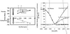
The top half ofFIG. 2 shows the tensile stress in thecurrent flow direction 21 and in-plane direction 22 on the tri-gate silicon channel in a tri-gate CMOS device, averaged over the tri-gate area, as a function of the pitch between the N-type and P-type channels, and further assuming a copper metal fill that is intrinsically 1% stressed compared to the relaxed state. The compressive stress in the surfacenormal direction 23 on the tri-gate silicon channel in the surface normal direction is shown in the bottom half ofFIG. 2 , also intrinsically 1% stressed compared to the relaxed state. “W_Pitch” is the distance between individual channels, of a particular type of multi-fin device for example multi-fin N-type or multi-fin P-type devices. Increasing tensile stress is shown increasing in the upward direction in the top half ofFIG. 2 . Increasing compressive stress is shown increasing in the downward direction in the bottom half ofFIG. 2 .
Other embodiments contemplate methods of fabricating the above-described embodiments, methods of using the above-described embodiments, and apparatus or systems using the above-described embodiments.
This application may disclose several numerical range limitations that support any range within the disclosed numerical ranges even though a precise range limitation is not stated verbatim in the specification because the embodiments could be practiced throughout the disclosed numerical ranges. Finally, the entire disclosure of the patents and publications referred in this application, if any, are hereby incorporated herein in entirety by reference.
Claims (5)
1. A method, comprising:
raising a first channel comprising an N-type material above a substrate, the first channel having a first top surface, a first pair of sidewalls, and a first current flow direction along a first major axis of the first channel;
raising a second channel comprising a P-type material above the substrate, the second channel having a second top surface, a second pair of sidewalls, and a second current flow direction along a second major axis of the second channel;
depositing a first gate around the first top surface and the first pair of sidewalls of the first channel and substantially perpendicular to the major axis, wherein the first gate comprises a first intrinsically stressed metal fill in which intrinsic stress of the first intrinsically stressed metal fill exerts a tensile stress upon the first channel such that charge carrier mobility in the first channel is improved in the first current flow direction; and
depositing a second gate around the second top surface and the second pair of sidewalls of the second channel and substantially perpendicular to the second major axis, wherein the second gate comprises a second intrinsically stressed metal fill in which intrinsic stress of the second intrinsically stressed metal fill exerts a compressive stress upon the second channel such that charge carrier mobility in the second channel is improved in the second current flow direction.
2. The method ofclaim 1 , further comprising isolating the-first channel using a shallow trench isolation layer.
3. The method ofclaim 1 , further comprising isolating the first channel, from the second channel, by using a shallow trench isolation layer.
4. The method ofclaim 1 , wherein depositing the first gate comprises depositing an intrinsically compressively stressed copper metal fill that exerts the tensile stress upon the first channel such that the charge carrier mobility in the first channel is improved in the first current flow direction.
5. The method ofclaim 4 , wherein depositing the second gate comprises depositing an intrinsically tensilely stressed tungsten metal fill that exerts the compressive stress upon the second channel such that the charge carrier mobility in the second channel is improved in the second current flow direction.
Priority Applications (4)
| Application Number | Priority Date | Filing Date | Title |
|---|---|---|---|
| US13/750,393US8741733B2 (en) | 2008-06-23 | 2013-01-25 | Stress in trigate devices using complimentary gate fill materials |
| US14/273,377US9224754B2 (en) | 2008-06-23 | 2014-05-08 | Stress in trigate devices using complimentary gate fill materials |
| US14/938,812US9450092B2 (en) | 2008-06-23 | 2015-11-11 | Stress in trigate devices using complimentary gate fill materials |
| US15/250,836US9806193B2 (en) | 2008-06-23 | 2016-08-29 | Stress in trigate devices using complimentary gate fill materials |
Applications Claiming Priority (2)
| Application Number | Priority Date | Filing Date | Title |
|---|---|---|---|
| US12/144,469US8362566B2 (en) | 2008-06-23 | 2008-06-23 | Stress in trigate devices using complimentary gate fill materials |
| US13/750,393US8741733B2 (en) | 2008-06-23 | 2013-01-25 | Stress in trigate devices using complimentary gate fill materials |
Related Parent Applications (1)
| Application Number | Title | Priority Date | Filing Date |
|---|---|---|---|
| US12/144,469DivisionUS8362566B2 (en) | 2008-06-23 | 2008-06-23 | Stress in trigate devices using complimentary gate fill materials |
Related Child Applications (1)
| Application Number | Title | Priority Date | Filing Date |
|---|---|---|---|
| US14/273,377ContinuationUS9224754B2 (en) | 2008-06-23 | 2014-05-08 | Stress in trigate devices using complimentary gate fill materials |
Publications (2)
| Publication Number | Publication Date |
|---|---|
| US20130143385A1 US20130143385A1 (en) | 2013-06-06 |
| US8741733B2true US8741733B2 (en) | 2014-06-03 |
Family
ID=41430329
Family Applications (5)
| Application Number | Title | Priority Date | Filing Date |
|---|---|---|---|
| US12/144,469Expired - Fee RelatedUS8362566B2 (en) | 2008-06-23 | 2008-06-23 | Stress in trigate devices using complimentary gate fill materials |
| US13/750,393Expired - Fee RelatedUS8741733B2 (en) | 2008-06-23 | 2013-01-25 | Stress in trigate devices using complimentary gate fill materials |
| US14/273,377ActiveUS9224754B2 (en) | 2008-06-23 | 2014-05-08 | Stress in trigate devices using complimentary gate fill materials |
| US14/938,812ActiveUS9450092B2 (en) | 2008-06-23 | 2015-11-11 | Stress in trigate devices using complimentary gate fill materials |
| US15/250,836ActiveUS9806193B2 (en) | 2008-06-23 | 2016-08-29 | Stress in trigate devices using complimentary gate fill materials |
Family Applications Before (1)
| Application Number | Title | Priority Date | Filing Date |
|---|---|---|---|
| US12/144,469Expired - Fee RelatedUS8362566B2 (en) | 2008-06-23 | 2008-06-23 | Stress in trigate devices using complimentary gate fill materials |
Family Applications After (3)
| Application Number | Title | Priority Date | Filing Date |
|---|---|---|---|
| US14/273,377ActiveUS9224754B2 (en) | 2008-06-23 | 2014-05-08 | Stress in trigate devices using complimentary gate fill materials |
| US14/938,812ActiveUS9450092B2 (en) | 2008-06-23 | 2015-11-11 | Stress in trigate devices using complimentary gate fill materials |
| US15/250,836ActiveUS9806193B2 (en) | 2008-06-23 | 2016-08-29 | Stress in trigate devices using complimentary gate fill materials |
Country Status (1)
| Country | Link |
|---|---|
| US (5) | US8362566B2 (en) |
Families Citing this family (12)
| Publication number | Priority date | Publication date | Assignee | Title |
|---|---|---|---|---|
| US8518811B2 (en) | 2011-04-08 | 2013-08-27 | Infineon Technologies Ag | Schottky diodes having metal gate electrodes and methods of formation thereof |
| US8693235B2 (en)* | 2011-12-06 | 2014-04-08 | Taiwan Semiconductor Manufacturing Company, Ltd. | Methods and apparatus for finFET SRAM arrays in integrated circuits |
| KR101700213B1 (en) | 2011-12-21 | 2017-01-26 | 인텔 코포레이션 | Methods for forming fins for metal oxide semiconductor device structures |
| US8716751B2 (en) | 2012-09-28 | 2014-05-06 | Intel Corporation | Methods of containing defects for non-silicon device engineering |
| CN103779413B (en) | 2012-10-19 | 2016-09-07 | 中芯国际集成电路制造(上海)有限公司 | Semiconductor devices and manufacture method thereof |
| US9780211B2 (en) | 2012-12-31 | 2017-10-03 | Taiwan Semiconductor Manufacturing Company, Ltd. | Power cell and power cell circuit for a power amplifier |
| US10593600B2 (en)* | 2016-02-24 | 2020-03-17 | International Business Machines Corporation | Distinct gate stacks for III-V-based CMOS circuits comprising a channel cap |
| US10062693B2 (en) | 2016-02-24 | 2018-08-28 | International Business Machines Corporation | Patterned gate dielectrics for III-V-based CMOS circuits |
| US9653602B1 (en) | 2016-03-21 | 2017-05-16 | International Business Machines Corporation | Tensile and compressive fins for vertical field effect transistors |
| KR102618607B1 (en)* | 2016-09-06 | 2023-12-26 | 삼성전자주식회사 | Semiconductor device and method for fabricating the same |
| US11114471B2 (en) | 2017-09-26 | 2021-09-07 | Intel Corporation | Thin film transistors having relatively increased width and shared bitlines |
| US11948939B2 (en)* | 2021-01-13 | 2024-04-02 | Taiwan Semiconductor Manufacturing Company, Ltd | Profile control of gate structures in semiconductor devices |
Citations (499)
| Publication number | Priority date | Publication date | Assignee | Title |
|---|---|---|---|---|
| US3387820A (en) | 1965-05-24 | 1968-06-11 | Continental Aviat & Engineerin | Turbine engine construction |
| US4231149A (en) | 1978-10-10 | 1980-11-04 | Texas Instruments Incorporated | Narrow band-gap semiconductor CCD imaging device and method of fabrication |
| US4487652A (en) | 1984-03-30 | 1984-12-11 | Motorola, Inc. | Slope etch of polyimide |
| GB2156149A (en) | 1984-03-14 | 1985-10-02 | Philips Electronic Associated | Dielectrically-isolated integrated circuit manufacture |
| US4711701A (en) | 1986-09-16 | 1987-12-08 | Texas Instruments Incorporated | Self-aligned transistor method |
| EP0265314A1 (en) | 1986-10-06 | 1988-04-27 | France Telecom | Method of forming an insulating layer of a sulphide, sulphur compounds obtained and device to carry out the method |
| US4751201A (en) | 1987-03-04 | 1988-06-14 | Bell Communications Research, Inc. | Passivation of gallium arsenide devices with sodium sulfide |
| US4818715A (en) | 1987-07-09 | 1989-04-04 | Industrial Technology Research Institute | Method of fabricating a LDDFET with self-aligned silicide |
| US4871692A (en) | 1988-09-30 | 1989-10-03 | Lee Hong H | Passivation of group III-V surfaces |
| US4872046A (en) | 1986-01-24 | 1989-10-03 | University Of Illinois | Heterojunction semiconductor device with <001> tilt |
| US4905063A (en) | 1988-06-21 | 1990-02-27 | American Telephone And Telegraph Company, At&T Bell Laboratories | Floating gate memories |
| US4907048A (en) | 1987-11-23 | 1990-03-06 | Xerox Corporation | Double implanted LDD transistor self-aligned with gate |
| US4906589A (en) | 1989-02-06 | 1990-03-06 | Industrial Technology Research Institute | Inverse-T LDDFET with self-aligned silicide |
| US4914059A (en) | 1986-10-27 | 1990-04-03 | Yves Nissim | Process for the heat flash vapour phase deposition of an insulating layer on a III-V material substrate and its application to the production of a MIS structure |
| US4994873A (en) | 1988-10-17 | 1991-02-19 | Motorola, Inc. | Local interconnect for stacked polysilicon device |
| US4996574A (en) | 1988-07-01 | 1991-02-26 | Fujitsu Limited | MIS transistor structure for increasing conductance between source and drain regions |
| US5023203A (en) | 1988-07-28 | 1991-06-11 | Korea Electronics & Telecommunications Research Institute Et Al. | Method of patterning fine line width semiconductor topology using a spacer |
| EP0469604A2 (en) | 1990-08-01 | 1992-02-05 | Sumitomo Electric Industries, Limited | MIS electrode forming process |
| US5120666A (en) | 1989-05-16 | 1992-06-09 | Fujitsu Limited | Manufacturing method for semiconductor device |
| US5124777A (en) | 1990-07-02 | 1992-06-23 | Samsung Electronics Co., Ltd. | Dielectric medium for capacitor of semiconductor device |
| US5179037A (en) | 1991-12-24 | 1993-01-12 | Texas Instruments Incorporated | Integration of lateral and vertical quantum well transistors in the same epitaxial stack |
| US5216271A (en) | 1990-09-28 | 1993-06-01 | Kabushiki Kaisha Toshiba | BiCMOS device with low bandgap CMOS contact regions and low bandgap bipolar base region |
| US5218213A (en) | 1991-02-22 | 1993-06-08 | Harris Corporation | SOI wafer with sige |
| US5278012A (en) | 1989-03-29 | 1994-01-11 | Hitachi, Ltd. | Method for producing thin film multilayer substrate, and method and apparatus for detecting circuit conductor pattern of the substrate |
| US5278102A (en) | 1990-08-18 | 1994-01-11 | Fujitsu Limited | SOI device and a fabrication process thereof |
| US5308999A (en) | 1992-02-27 | 1994-05-03 | Fujitsu Limited | MOS FET having a thin film SOI structure |
| EP0474952B1 (en) | 1990-09-14 | 1994-06-01 | International Business Machines Corporation | A method of passivating etched mirror facets of semiconductor lasers |
| US5328810A (en) | 1990-05-07 | 1994-07-12 | Micron Technology, Inc. | Method for reducing, by a factor or 2-N, the minimum masking pitch of a photolithographic process |
| US5338959A (en) | 1992-03-30 | 1994-08-16 | Samsung Electronics Co., Ltd. | Thin film transistor with three dimensional multichannel structure |
| US5346836A (en) | 1991-06-06 | 1994-09-13 | Micron Technology, Inc. | Process for forming low resistance contacts between silicide areas and upper level polysilicon interconnects |
| US5346839A (en) | 1991-06-10 | 1994-09-13 | Texas Instruments Incorporated | Sidewall doping technique for SOI transistors |
| US5357119A (en) | 1993-02-19 | 1994-10-18 | Board Of Regents Of The University Of California | Field effect devices having short period superlattice structures using Si and Ge |
| EP0623963A1 (en) | 1993-05-06 | 1994-11-09 | Siemens Aktiengesellschaft | MOSFET on SOI substrate |
| US5371024A (en) | 1988-09-30 | 1994-12-06 | Kabushiki Kaisha Toshiba | Semiconductor device and process for manufacturing the same |
| US5391506A (en) | 1992-01-31 | 1995-02-21 | Kawasaki Steel Corporation | Manufacturing method for semiconductor devices with source/drain formed in substrate projection. |
| US5398641A (en) | 1993-07-27 | 1995-03-21 | Texas Instruments Incorporated | Method for p-type doping of semiconductor structures formed of group II and group VI elements |
| US5428237A (en) | 1991-04-26 | 1995-06-27 | Canon Kabushiki Kaisha | Semiconductor device having an insulated gate transistor |
| US5466621A (en) | 1988-11-21 | 1995-11-14 | Hitachi, Ltd. | Method of manufacturing a semiconductor device having silicon islands |
| US5475869A (en) | 1993-05-28 | 1995-12-12 | Nec Corporation | Radio base station capable of distinguishing between interference due to collisions of outgoing call signals and an external interference noise |
| US5479033A (en) | 1994-05-27 | 1995-12-26 | Sandia Corporation | Complementary junction heterostructure field-effect transistor |
| US5482877A (en) | 1993-02-17 | 1996-01-09 | Samsung Electronics Co., Ltd. | Method for making a semiconductor device having a silicon-on-insulator structure |
| US5495115A (en) | 1993-08-06 | 1996-02-27 | Hitachi, Ltd. | Semiconductor crystalline laminate structure, forming method of the same, and semiconductor device employing the same |
| US5514885A (en) | 1986-10-09 | 1996-05-07 | Myrick; James J. | SOI methods and apparatus |
| US5521859A (en) | 1991-03-20 | 1996-05-28 | Fujitsu Limited | Semiconductor memory device having thin film transistor and method of producing the same |
| US5539229A (en) | 1994-12-28 | 1996-07-23 | International Business Machines Corporation | MOSFET with raised STI isolation self-aligned to the gate stack |
| US5543351A (en) | 1992-03-19 | 1996-08-06 | Matsushita Electric Industrial Co., Ltd. | Method of producing electrically insulated silicon structure |
| US5545586A (en) | 1990-11-27 | 1996-08-13 | Nec Corporation | Method of making a transistor having easily controllable impurity profile |
| US5554870A (en) | 1994-02-04 | 1996-09-10 | Motorola, Inc. | Integrated circuit having both vertical and horizontal devices and process for making the same |
| US5563077A (en) | 1992-04-24 | 1996-10-08 | Hyundai Electronics Industries Co., Ltd. | Method of fabricating a thin film transistor having vertical channel |
| US5576227A (en) | 1994-11-02 | 1996-11-19 | United Microelectronics Corp. | Process for fabricating a recessed gate MOS device |
| US5578513A (en) | 1993-09-17 | 1996-11-26 | Mitsubishi Denki Kabushiki Kaisha | Method of making a semiconductor device having a gate all around type of thin film transistor |
| US5595941A (en) | 1994-06-01 | 1997-01-21 | Mitsubishi Denki Kabushiki Kaisha | Method of forming fine patterns |
| US5595919A (en) | 1996-02-20 | 1997-01-21 | Chartered Semiconductor Manufacturing Pte Ltd. | Method of making self-aligned halo process for reducing junction capacitance |
| US5652454A (en) | 1993-07-05 | 1997-07-29 | Iwamatsu; Toshiaki | Semiconductor device on an SOI substrate |
| US5658806A (en) | 1995-10-26 | 1997-08-19 | National Science Council | Method for fabricating thin-film transistor with bottom-gate or dual-gate configuration |
| US5665203A (en) | 1995-04-28 | 1997-09-09 | International Business Machines Corporation | Silicon etching method |
| US5682048A (en) | 1995-05-19 | 1997-10-28 | Nissan Motor Co., Ltd. | Groove-type semiconductor device |
| US5698869A (en) | 1994-09-13 | 1997-12-16 | Kabushiki Kaisha Toshiba | Insulated-gate transistor having narrow-bandgap-source |
| US5701016A (en) | 1994-11-24 | 1997-12-23 | Kabushiki Kaisha Toshiba | Semiconductor device and method for its manufacture |
| US5716879A (en) | 1994-12-15 | 1998-02-10 | Goldstar Electron Company, Ltd. | Method of making a thin film transistor |
| US5739544A (en) | 1993-05-26 | 1998-04-14 | Matsushita Electric Industrial Co., Ltd. | Quantization functional device utilizing a resonance tunneling effect and method for producing the same |
| US5760442A (en) | 1994-09-29 | 1998-06-02 | Kabushiki Kaisha Toshiba | Semiconductor device of a silicon on insulator metal-insulator type with a concave feature |
| US5770513A (en) | 1993-02-25 | 1998-06-23 | Mitsubishi Denki Kabushiki Kaisha | Method for producing semiconductor device with heat dissipation structure |
| US5773331A (en) | 1996-12-17 | 1998-06-30 | International Business Machines Corporation | Method for making single and double gate field effect transistors with sidewall source-drain contacts |
| US5776821A (en) | 1997-08-22 | 1998-07-07 | Vlsi Technology, Inc. | Method for forming a reduced width gate electrode |
| US5793088A (en) | 1996-06-18 | 1998-08-11 | Integrated Device Technology, Inc. | Structure for controlling threshold voltage of MOSFET |
| US5804848A (en) | 1995-01-20 | 1998-09-08 | Sony Corporation | Field effect transistor having multiple gate electrodes surrounding the channel region |
| US5811324A (en) | 1995-12-26 | 1998-09-22 | Lg Semicon Co., Ltd. | Method for manufacturing thin film transistor |
| US5814895A (en) | 1995-12-22 | 1998-09-29 | Sony Corporation | Static random access memory having transistor elements formed on side walls of a trench in a semiconductor substrate |
| US5814545A (en) | 1995-10-02 | 1998-09-29 | Motorola, Inc. | Semiconductor device having a phosphorus doped PECVD film and a method of manufacture |
| US5821629A (en) | 1994-10-04 | 1998-10-13 | United Microelectronics Corporation | Buried structure SRAM cell and methods for fabrication |
| US5827769A (en) | 1996-11-20 | 1998-10-27 | Intel Corporation | Method for fabricating a transistor with increased hot carrier resistance by nitridizing and annealing the sidewall oxide of the gate electrode |
| US5844278A (en) | 1994-09-14 | 1998-12-01 | Kabushiki Kaisha Toshiba | Semiconductor device having a projecting element region |
| US5856225A (en) | 1997-11-24 | 1999-01-05 | Chartered Semiconductor Manufacturing Ltd | Creation of a self-aligned, ion implanted channel region, after source and drain formation |
| US5859456A (en) | 1994-11-02 | 1999-01-12 | Texas Instruments Incorporated | Multiple transistor integrated circuit with thick copper interconnect |
| US5880015A (en) | 1991-04-30 | 1999-03-09 | Sgs-Thomson Microelectronics, Inc. | Method of producing stepped wall interconnects and gates |
| US5883564A (en) | 1994-04-18 | 1999-03-16 | General Motors Corporation | Magnetic field sensor having high mobility thin indium antimonide active layer on thin aluminum indium antimonide buffer layer |
| US5889304A (en) | 1996-06-28 | 1999-03-30 | Kabushiki Kaisha Toshiba | Nonvolatile semiconductor memory device |
| US5888309A (en) | 1997-12-29 | 1999-03-30 | Taiwan Semiconductor Manufacturing Company, Ltd. | Lateral etch inhibited multiple for forming a via through a microelectronics layer susceptible to etching within a fluorine containing plasma followed by an oxygen containing plasma |
| US5905285A (en) | 1996-09-12 | 1999-05-18 | Advanced Micro Devices, Inc. | Ultra short trench transistors and process for making same |
| US5908313A (en) | 1996-12-31 | 1999-06-01 | Intel Corporation | Method of forming a transistor |
| US5952701A (en) | 1997-08-18 | 1999-09-14 | National Semiconductor Corporation | Design and fabrication of semiconductor structure having complementary channel-junction insulated-gate field-effect transistors whose gate electrodes have work functions close to mid-gap semiconductor value |
| US5965914A (en) | 1997-06-18 | 1999-10-12 | Mitsubishi Denki Kabushiki Kaisha | Thin film transistor having a branched gate and channel |
| US5976767A (en) | 1997-10-09 | 1999-11-02 | Micron Technology, Inc. | Ammonium hydroxide etch of photoresist masked silicon |
| US5981400A (en) | 1997-09-18 | 1999-11-09 | Cornell Research Foundation, Inc. | Compliant universal substrate for epitaxial growth |
| US5985726A (en) | 1998-11-06 | 1999-11-16 | Advanced Micro Devices, Inc. | Damascene process for forming ultra-shallow source/drain extensions and pocket in ULSI MOSFET |
| US6013926A (en) | 1996-11-20 | 2000-01-11 | Mitsubishi Denki Kabushiki Kaisha | Semiconductor device with refractory metal element |
| US6018176A (en) | 1995-05-26 | 2000-01-25 | Samsung Electronics Co., Ltd. | Vertical transistor and memory cell |
| JP2000037842A (en) | 1998-07-27 | 2000-02-08 | Dainippon Printing Co Ltd | Electromagnetic wave absorbing cosmetic material |
| US6031249A (en) | 1996-07-11 | 2000-02-29 | Semiconductor Energy Laboratory Co., Ltd. | CMOS semiconductor device having boron doped channel |
| US6054355A (en) | 1997-06-30 | 2000-04-25 | Kabushiki Kaisha Toshiba | Method of manufacturing a semiconductor device which includes forming a dummy gate |
| US6063677A (en) | 1996-10-28 | 2000-05-16 | Texas Instruments Incorporated | Method of forming a MOSFET using a disposable gate and raised source and drain |
| US6063675A (en) | 1996-10-28 | 2000-05-16 | Texas Instruments Incorporated | Method of forming a MOSFET using a disposable gate with a sidewall dielectric |
| US6066869A (en) | 1997-10-06 | 2000-05-23 | Micron Technology, Inc. | Circuit and method for a folded bit line memory cell with vertical transistor and trench capacitor |
| US6087208A (en) | 1998-03-31 | 2000-07-11 | Advanced Micro Devices, Inc. | Method for increasing gate capacitance by using both high and low dielectric gate material |
| US6093621A (en) | 1999-04-05 | 2000-07-25 | Vanguard International Semiconductor Corp. | Method of forming shallow trench isolation |
| US6114206A (en) | 1998-11-06 | 2000-09-05 | Advanced Micro Devices, Inc. | Multiple threshold voltage transistor implemented by a damascene process |
| US6114201A (en) | 1998-06-01 | 2000-09-05 | Texas Instruments-Acer Incorporated | Method of manufacturing a multiple fin-shaped capacitor for high density DRAMs |
| US6117697A (en) | 1998-07-27 | 2000-09-12 | The United States Of America As Represented By The Secretary Of The Air Force | Solid state magnetic field sensor method |
| US6117741A (en) | 1998-01-09 | 2000-09-12 | Texas Instruments Incorporated | Method of forming a transistor having an improved sidewall gate structure |
| US6120846A (en) | 1997-12-23 | 2000-09-19 | Advanced Technology Materials, Inc. | Method for the selective deposition of bismuth based ferroelectric thin films by chemical vapor deposition |
| US6130123A (en) | 1998-06-30 | 2000-10-10 | Intel Corporation | Method for making a complementary metal gate electrode technology |
| US6133106A (en)* | 1998-02-23 | 2000-10-17 | Sharp Laboratories Of America, Inc. | Fabrication of a planar MOSFET with raised source/drain by chemical mechanical polishing and nitride replacement |
| US6133593A (en) | 1999-07-23 | 2000-10-17 | The United States Of America As Represented By The Secretary Of The Navy | Channel design to reduce impact ionization in heterostructure field-effect transistors |
| US6144072A (en) | 1994-11-02 | 2000-11-07 | Mitsubishi Denki Kabushiki Kaisha | Semiconductor device formed on insulating layer and method of manufacturing the same |
| US6150222A (en) | 1999-01-07 | 2000-11-21 | Advanced Micro Devices, Inc. | Method of making a high performance transistor with elevated spacer formation and self-aligned channel regions |
| US6153485A (en) | 1998-11-09 | 2000-11-28 | Chartered Semiconductor Manufacturing Ltd. | Salicide formation on narrow poly lines by pulling back of spacer |
| US6159808A (en) | 1999-11-12 | 2000-12-12 | United Semiconductor Corp. | Method of forming self-aligned DRAM cell |
| US6163053A (en) | 1996-11-06 | 2000-12-19 | Ricoh Company, Ltd. | Semiconductor device having opposite-polarity region under channel |
| US6165880A (en) | 1998-06-15 | 2000-12-26 | Taiwan Semiconductor Manufacturing Company | Double spacer technology for making self-aligned contacts (SAC) on semiconductor integrated circuits |
| US6174820B1 (en) | 1999-02-16 | 2001-01-16 | Sandia Corporation | Use of silicon oxynitride as a sacrificial material for microelectromechanical devices |
| US6190975B1 (en) | 1996-09-17 | 2001-02-20 | Matsushita Electric Industrial Co., Ltd. | Method of forming HCMOS devices with a silicon-germanium-carbon compound semiconductor layer |
| US6200865B1 (en) | 1998-12-04 | 2001-03-13 | Advanced Micro Devices, Inc. | Use of sacrificial dielectric structure to form semiconductor device with a self-aligned threshold adjust and overlying low-resistance gate |
| EP1091413A2 (en) | 1999-10-06 | 2001-04-11 | Lsi Logic Corporation | Fully-depleted, fully-inverted, short-length and vertical channel, dual-gate, cmos fet |
| US6218309B1 (en) | 1999-06-30 | 2001-04-17 | Lam Research Corporation | Method of achieving top rounding and uniform etch depths while etching shallow trench isolation features |
| US6251751B1 (en) | 1997-10-16 | 2001-06-26 | International Business Machines Corporation | Bulk and strained silicon on insulator using local selective oxidation |
| US6251729B1 (en) | 1998-12-18 | 2001-06-26 | U.S. Philips Corporation | Method of manufacturing a nonvolatile memory |
| US6252262B1 (en) | 1998-12-15 | 2001-06-26 | The United States Of America As Represented By The Secretary Of The Navy | Metal passivating layer for III-V semiconductors, and improved gate contact for III-V-based metal-insulator-semiconductor (MIS) devices |
| US6252284B1 (en) | 1999-12-09 | 2001-06-26 | International Business Machines Corporation | Planarized silicon fin device |
| US6251763B1 (en) | 1997-06-30 | 2001-06-26 | Kabushiki Kaisha Toshiba | Semiconductor device and method for manufacturing same |
| US6259135B1 (en) | 1999-09-24 | 2001-07-10 | International Business Machines Corporation | MOS transistors structure for reducing the size of pitch limited circuits |
| US6261921B1 (en) | 1999-07-31 | 2001-07-17 | Taiwan Semiconductor Manufacturing Co., Ltd. | Method of forming shallow trench isolation structure |
| US6262456B1 (en) | 1998-11-06 | 2001-07-17 | Advanced Micro Devices, Inc. | Integrated circuit having transistors with different threshold voltages |
| US6274503B1 (en) | 1998-12-18 | 2001-08-14 | United Microelectronics Corp. | Etching method for doped polysilicon layer |
| US20010019886A1 (en) | 1998-05-12 | 2001-09-06 | International Business Machines Corporation | Borderless contact to diffusion with respect to gate conductor and methods for fabricating |
| US6287924B1 (en) | 1998-09-21 | 2001-09-11 | Texas Instruments Incorporated | Integrated circuit and method |
| US6294416B1 (en) | 1998-01-23 | 2001-09-25 | Texas Instruments-Acer Incorporated | Method of fabricating CMOS transistors with self-aligned planarization twin-well by using fewer mask counts |
| US20010026985A1 (en) | 2000-03-29 | 2001-10-04 | Kim Moon Jung | Fabrication method of submicron gate using anisotropic etching |
| US6307235B1 (en) | 1998-03-30 | 2001-10-23 | Micron Technology, Inc. | Another technique for gated lateral bipolar transistors |
| US6310367B1 (en) | 1999-02-22 | 2001-10-30 | Kabushiki Kaisha Toshiba | MOS transistor having a tensile-strained SI layer and a compressive-strained SI-GE layer |
| US6317444B1 (en) | 1998-06-12 | 2001-11-13 | Agere System Optoelectronics Guardian Corp. | Optical device including carbon-doped contact layers |
| US6319807B1 (en) | 2000-02-07 | 2001-11-20 | United Microelectronics Corp. | Method for forming a semiconductor device by using reverse-offset spacer process |
| US6320212B1 (en) | 1999-09-02 | 2001-11-20 | Hrl Laboratories, Llc. | Superlattice fabrication for InAs/GaSb/AISb semiconductor structures |
| JP2001338987A (en) | 2000-05-26 | 2001-12-07 | Nec Microsystems Ltd | Forming method of shallow trench isolation region of mos transistor |
| US6335251B2 (en) | 1998-05-29 | 2002-01-01 | Kabushiki Kaisha Toshiba | Semiconductor apparatus having elevated source and drain structure and manufacturing method therefor |
| US20020011612A1 (en) | 2000-07-31 | 2002-01-31 | Kabushiki Kaisha Toshiba | Semiconductor device and method for manufacturing the same |
| US6358800B1 (en) | 2000-09-18 | 2002-03-19 | Vanguard International Semiconductor Corporation | Method of forming a MOSFET with a recessed-gate having a channel length beyond photolithography limit |
| US6359311B1 (en) | 2001-01-17 | 2002-03-19 | Taiwan Semiconductor Manufacturing Co., Ltd. | Quasi-surrounding gate and a method of fabricating a silicon-on-insulator semiconductor device with the same |
| US6362111B1 (en) | 1998-12-09 | 2002-03-26 | Texas Instruments Incorporated | Tunable gate linewidth reduction process |
| US20020036290A1 (en) | 2000-09-28 | 2002-03-28 | Kabushiki Kaisha Toshiba | Semiconductor device having MIS field effect transistors or three-dimensional structure |
| US20020037619A1 (en) | 2000-09-22 | 2002-03-28 | Kohei Sugihara | Semiconductor device and method of producing the same |
| US6368923B1 (en) | 2000-04-20 | 2002-04-09 | United Microelectronics Corp. | Method of fabricating a dual metal gate having two different gate dielectric layers |
| JP2002110977A (en) | 2000-06-27 | 2002-04-12 | Samsung Electronics Co Ltd | Nano-sized vertical transistor using carbon nanotube and method of manufacturing the same |
| US6376317B1 (en) | 1998-03-30 | 2002-04-23 | Micron Technology, Inc. | Methods for dual-gated transistors |
| US20020048918A1 (en) | 2000-10-19 | 2002-04-25 | Grider Douglas T. | Multi-layered polysilicon process |
| EP1202335A2 (en) | 2000-10-18 | 2002-05-02 | International Business Machines Corporation | Method of fabricating semiconductor side wall fin |
| US6383882B1 (en) | 2000-08-21 | 2002-05-07 | Samsung Electronics Co., Ltd. | Method for fabricating MOS transistor using selective silicide process |
| US6387820B1 (en) | 2000-09-19 | 2002-05-14 | Advanced Micro Devices, Inc. | BC13/AR chemistry for metal overetching on a high density plasma etcher |
| US20020058374A1 (en) | 2000-11-16 | 2002-05-16 | Tae-Kyun Kim | Method of forming dual-metal gates in semiconductor device |
| US6391782B1 (en) | 2000-06-20 | 2002-05-21 | Advanced Micro Devices, Inc. | Process for forming multiple active lines and gate-all-around MOSFET |
| US6396108B1 (en) | 2000-11-13 | 2002-05-28 | Advanced Micro Devices, Inc. | Self-aligned double gate silicon-on-insulator (SOI) device |
| WO2002043151A1 (en) | 2000-11-22 | 2002-05-30 | Hitachi, Ltd | Semiconductor device and method for fabricating the same |
| US6403981B1 (en) | 2000-08-07 | 2002-06-11 | Advanced Micro Devices, Inc. | Double gate transistor having a silicon/germanium channel region |
| US6403434B1 (en) | 2001-02-09 | 2002-06-11 | Advanced Micro Devices, Inc. | Process for manufacturing MOS transistors having elevated source and drain regions and a high-k gate dielectric |
| US6407442B2 (en) | 1994-10-28 | 2002-06-18 | Canon Kabushiki Kaisha | Semiconductor device, and operating device, signal converter, and signal processing system using the same semiconductor device |
| US6406795B1 (en) | 1998-11-25 | 2002-06-18 | Applied Optoelectronics, Inc. | Compliant universal substrates for optoelectronic and electronic devices |
| US20020074614A1 (en) | 2000-12-15 | 2002-06-20 | Mitsubishi Denki Kabushiki Kaisha | Semiconductor device and manufacturing method therefor |
| US6410371B1 (en) | 2001-02-26 | 2002-06-25 | Advanced Micro Devices, Inc. | Method of fabrication of semiconductor-on-insulator (SOI) wafer having a Si/SiGe/Si active layer |
| US20020081794A1 (en) | 2000-12-26 | 2002-06-27 | Nec Corporation | Enhanced deposition control in fabricating devices in a semiconductor wafer |
| US6413802B1 (en) | 2000-10-23 | 2002-07-02 | The Regents Of The University Of California | Finfet transistor structures having a double gate channel extending vertically from a substrate and methods of manufacture |
| US6413877B1 (en) | 2000-12-22 | 2002-07-02 | Lam Research Corporation | Method of preventing damage to organo-silicate-glass materials during resist stripping |
| US6424015B1 (en) | 1999-06-29 | 2002-07-23 | Hitachi, Ltd. | Semiconductor integrated circuit device |
| US6437550B2 (en) | 1999-12-28 | 2002-08-20 | Ricoh Company, Ltd. | Voltage generating circuit and reference voltage source circuit employing field effect transistors |
| US6457890B1 (en) | 1996-02-26 | 2002-10-01 | Gregor Kohlruss | Device for cleaning flat objects |
| US6458662B1 (en) | 2001-04-04 | 2002-10-01 | Advanced Micro Devices, Inc. | Method of fabricating a semiconductor device having an asymmetrical dual-gate silicon-germanium (SiGe) channel MOSFET and a device thereby formed |
| US6459123B1 (en) | 1999-04-30 | 2002-10-01 | Infineon Technologies Richmond, Lp | Double gated transistor |
| US20020142529A1 (en) | 2001-03-29 | 2002-10-03 | Satoshi Matsuda | Semiconductor device comprising buried channel region and method for manufacturing the same |
| JP2002298051A (en) | 2001-03-30 | 2002-10-11 | Mizuho Bank Ltd | Point exchange service system |
| US6465290B1 (en) | 2000-03-27 | 2002-10-15 | Kabushiki Kaisha Toshiba | Method of manufacturing a semiconductor device using a polymer film pattern |
| US6466621B1 (en) | 1999-03-26 | 2002-10-15 | Koninklijke Philips Electronics N.V. | Video coding method and corresponding video coder |
| US20020149031A1 (en) | 2001-04-12 | 2002-10-17 | Samsung Electronics Co., Ltd. | Semiconductor device having gate all around type transistor and method of forming the same |
| US6472258B1 (en) | 2000-11-13 | 2002-10-29 | International Business Machines Corporation | Double gate trench transistor |
| US20020160553A1 (en) | 2001-02-14 | 2002-10-31 | Hideo Yamanaka | Method and apparatus for forming a thin semiconductor film, method and apparatus for producing a semiconductor device, and electro-opitcal apparatus |
| TW508669B (en) | 1999-11-30 | 2002-11-01 | Infineon Technologies Corp | Process for fabricating a uniform gate oxide of a vertical transistor |
| US6475890B1 (en) | 2001-02-12 | 2002-11-05 | Advanced Micro Devices, Inc. | Fabrication of a field effect transistor with an upside down T-shaped semiconductor pillar in SOI technology |
| US6475869B1 (en) | 2001-02-26 | 2002-11-05 | Advanced Micro Devices, Inc. | Method of forming a double gate transistor having an epitaxial silicon/germanium channel region |
| US6479866B1 (en) | 2000-11-14 | 2002-11-12 | Advanced Micro Devices, Inc. | SOI device with self-aligned selective damage implant, and method |
| US20020166838A1 (en) | 2001-05-10 | 2002-11-14 | Institute Of Microelectronics | Sloped trench etching process |
| US20020167007A1 (en) | 1998-12-29 | 2002-11-14 | Semiconductor Energy Laboratory Co., Ltd. | Semiconductor device and method of fabricating the same |
| US6483156B1 (en) | 2000-03-16 | 2002-11-19 | International Business Machines Corporation | Double planar gated SOI MOSFET structure |
| US6483151B2 (en) | 2000-01-21 | 2002-11-19 | Nec Corporation | Semiconductor device and method of manufacturing the same |
| US6483146B2 (en) | 1999-12-13 | 2002-11-19 | Samsung Electronics Co., Ltd. | Nonvolatile semiconductor memory device and manufacturing method thereof |
| US20020177282A1 (en) | 2001-05-23 | 2002-11-28 | Samsung Electronics Co., Ltd. | Method of forming semiconductor device having a GAA type transistor |
| US20020177263A1 (en) | 2001-05-24 | 2002-11-28 | International Business Machines Corporation | Damascene double-gate MOSFET with vertical channel regions |
| US20020185655A1 (en) | 2000-07-18 | 2002-12-12 | Fahimulla Ayub M. | Ultra-linear multi-channel field effect transistor |
| US6495403B1 (en) | 1999-10-05 | 2002-12-17 | Stmicroelectronics S.A. | Gate-all-around semiconductor device and process for fabricating the same |
| US6500767B2 (en) | 2001-03-20 | 2002-12-31 | Macronix International Co., Ltd. | Method of etching semiconductor metallic layer |
| US6501141B1 (en) | 2001-08-13 | 2002-12-31 | Taiwan Semiconductor Manufacturing Company, Ltd | Self-aligned contact with improved isolation and method for forming |
| TW516232B (en) | 1999-07-22 | 2003-01-01 | Ibm | Structure and process integration for producing transistors having independently adjustable parameters |
| US6506692B2 (en) | 2001-05-30 | 2003-01-14 | Intel Corporation | Method of making a semiconductor device using a silicon carbide hard mask |
| US6515339B2 (en) | 2000-07-18 | 2003-02-04 | Lg Electronics Inc. | Method of horizontally growing carbon nanotubes and field effect transistor using the carbon nanotubes grown by the method |
| US20030036290A1 (en) | 2001-08-17 | 2003-02-20 | United Microelectronics Corp. | Method for improving the coating capability of low-k dielectric layer |
| US6526996B1 (en) | 2000-06-12 | 2003-03-04 | Promos Technologies, Inc. | Dry clean method instead of traditional wet clean after metal etch |
| US20030042542A1 (en) | 1996-04-26 | 2003-03-06 | Shigeto Maegawa | Semiconductor device having a thin film transistor and manufacturing method thereof |
| US6534807B2 (en) | 2001-08-13 | 2003-03-18 | International Business Machines Corporation | Local interconnect junction on insulator (JOI) structure |
| US6537885B1 (en) | 2002-05-09 | 2003-03-25 | Infineon Technologies Ag | Transistor and method of manufacturing a transistor having a shallow junction formation using a two step EPI layer |
| US6537901B2 (en) | 2000-12-29 | 2003-03-25 | Hynix Semiconductor Inc. | Method of manufacturing a transistor in a semiconductor device |
| US20030057486A1 (en) | 2001-09-27 | 2003-03-27 | International Business Machines Corporation | Fin field effect transistor with self-aligned gate |
| US20030057477A1 (en) | 1999-06-18 | 2003-03-27 | Hergenrother John Michael | CMOS integrated circuit having vertical transistors and a process for fabricating same |
| US6541829B2 (en) | 1999-12-03 | 2003-04-01 | Kabushiki Kaisha Toshiba | Semiconductor device and method of manufacturing the same |
| US20030067017A1 (en) | 2001-10-05 | 2003-04-10 | Meikei Ieong | Variable threshold voltage double gated transistors and method of fabrication |
| US6555879B1 (en) | 2002-01-11 | 2003-04-29 | Advanced Micro Devices, Inc. | SOI device with metal source/drain and method of fabrication |
| US20030080332A1 (en) | 2000-05-19 | 2003-05-01 | Phillips Timothy J | Charge carrier extracting transistor |
| US20030080384A1 (en) | 2001-10-25 | 2003-05-01 | Matsushita Electric Industrial Co.., Ltd. | Semiconductor substrate, semiconductor device and method for fabricating the same |
| US20030085194A1 (en) | 2001-11-07 | 2003-05-08 | Hopkins Dean A. | Method for fabricating close spaced mirror arrays |
| US6562665B1 (en) | 2000-10-16 | 2003-05-13 | Advanced Micro Devices, Inc. | Fabrication of a field effect transistor with a recess in a semiconductor pillar in SOI technology |
| US6562687B1 (en) | 1999-01-15 | 2003-05-13 | Commissariat A L'energie Atomique | MIS transistor and method for making same on a semiconductor substrate |
| US20030098479A1 (en) | 1999-12-30 | 2003-05-29 | Anand Murthy | Novel MOS transistor structure and method of fabrication |
| US20030098488A1 (en) | 2001-11-27 | 2003-05-29 | O'keeffe James | Band-structure modulation of nano-structures in an electric field |
| US20030102497A1 (en) | 2001-12-04 | 2003-06-05 | International Business Machines Corporation | Multiple-plane finFET CMOS |
| US20030102518A1 (en) | 2001-12-04 | 2003-06-05 | International Business Machines Corporation | Finfet SRAM cell using low mobility plane for cell stability and method for forming |
| US20030111686A1 (en) | 2001-12-13 | 2003-06-19 | Nowak Edward J. | Method for forming asymmetric dual gate transistor |
| US6583469B1 (en) | 2002-01-28 | 2003-06-24 | International Business Machines Corporation | Self-aligned dog-bone structure for FinFET applications and methods to fabricate the same |
| US20030122186A1 (en) | 2001-03-13 | 2003-07-03 | Nat'l. Inst. Of Advanced Indust'l Sci. And Tech. | Double-gate field-effect transistor, integrated circuit using the transistor and method of manufacturing the same |
| US20030143791A1 (en) | 2002-01-29 | 2003-07-31 | Samsung Electronics Co., Ltd. | Methods for fabricating MOS transistors with notched gate electrodes |
| TW546713B (en) | 2001-06-12 | 2003-08-11 | Ibm | Relaxed SiGe layers on Si or silicon-on-insulator substrates by ion implantation and thermal annealing |
| US6605498B1 (en) | 2002-03-29 | 2003-08-12 | Intel Corporation | Semiconductor transistor having a backfilled channel material |
| US20030151077A1 (en) | 2002-02-13 | 2003-08-14 | Leo Mathew | Method of forming a vertical double gate semiconductor device and structure thereof |
| JP2003229575A (en) | 2002-02-04 | 2003-08-15 | Hitachi Ltd | Integrated semiconductor device and manufacturing method thereof |
| US6607948B1 (en) | 1998-12-24 | 2003-08-19 | Kabushiki Kaisha Toshiba | Method of manufacturing a substrate using an SiGe layer |
| TW548799B (en) | 2001-09-21 | 2003-08-21 | Mitsubishi Electric Corp | Method of manufacturing semiconductor device with offset sidewall structure |
| DE10203998A1 (en) | 2002-02-01 | 2003-08-21 | Infineon Technologies Ag | Production of a toothed structure in crystal structure in/on substrate used in production of floating gate transistor comprises forming trenches using a mask on the substrate and etching process and the unmasked region of substrate |
| US6611029B1 (en) | 2002-11-08 | 2003-08-26 | Advanced Micro Devices, Inc. | Double gate semiconductor device having separate gates |
| US20030174534A1 (en) | 2002-03-12 | 2003-09-18 | Clark Lawrence T. | Low standby power using shadow storage |
| US20030186167A1 (en) | 1999-11-29 | 2003-10-02 | Johnson Jr Alan T. | Fabrication of nanometer size gaps on an electrode |
| US20030190766A1 (en) | 2002-04-08 | 2003-10-09 | Micron Technology, Inc. | Process for making a silicon-on-insulator ledge and structures achieved thereby |
| JP2003298051A (en) | 2002-01-30 | 2003-10-17 | Soko Lee | Double gate FET device and method of manufacturing the same |
| US6635909B2 (en) | 2002-03-19 | 2003-10-21 | International Business Machines Corporation | Strained fin FETs structure and method |
| US20030203636A1 (en) | 2002-04-29 | 2003-10-30 | Anthony Thomas C. | Method of fabricating high density sub-lithographic features on a substrate |
| US6642114B2 (en) | 1997-01-29 | 2003-11-04 | Fujitsu Limited | Semiconductor device and method for fabricating the same |
| US6642090B1 (en) | 2002-06-03 | 2003-11-04 | International Business Machines Corporation | Fin FET devices from bulk semiconductor and method for forming |
| TW561530B (en) | 2001-01-03 | 2003-11-11 | Macronix Int Co Ltd | Process for fabricating CMOS transistor of IC devices employing double spacers for preventing short-channel effect |
| US6645797B1 (en) | 2002-12-06 | 2003-11-11 | Advanced Micro Devices, Inc. | Method for forming fins in a FinFET device using sacrificial carbon layer |
| US6645861B2 (en) | 2001-04-18 | 2003-11-11 | International Business Machines Corporation | Self-aligned silicide process for silicon sidewall source and drain contacts |
| US6660598B2 (en) | 2002-02-26 | 2003-12-09 | International Business Machines Corporation | Method of forming a fully-depleted SOI ( silicon-on-insulator) MOSFET having a thinned channel region |
| US20030227036A1 (en) | 2002-02-22 | 2003-12-11 | Naoharu Sugiyama | Semiconductor device |
| US6664160B2 (en) | 2000-06-28 | 2003-12-16 | Hyundai Electronics Industries Co., Ltd. | Gate structure with high K dielectric |
| US6680240B1 (en) | 2002-06-25 | 2004-01-20 | Advanced Micro Devices, Inc. | Silicon-on-insulator device with strained device film and method for making the same with partial replacement of isolation oxide |
| US20040016968A1 (en) | 2002-04-08 | 2004-01-29 | Stmicroelectronics S.A. | Surround-gate semiconductor device encapsulated in an insulating medium |
| US6686231B1 (en) | 2002-12-06 | 2004-02-03 | Advanced Micro Devices, Inc. | Damascene gate process with sacrificial oxide in semiconductor devices |
| US20040029393A1 (en) | 2002-08-12 | 2004-02-12 | Applied Materials, Inc. | Method for removal of residue from a magneto-resistive random access memory (MRAM) film stack using a sacrificial mask layer |
| US20040029345A1 (en) | 2000-06-09 | 2004-02-12 | Simon Deleonibus | Damascene architecture electronics storage and method for making same |
| TW200402872A (en) | 2002-03-05 | 2004-02-16 | Sharp Kk | Semiconductor memory device |
| US20040031979A1 (en) | 2002-06-07 | 2004-02-19 | Amberwave Systems Corporation | Strained-semiconductor-on-insulator device structures |
| US20040033639A1 (en) | 2001-05-07 | 2004-02-19 | Applied Materials, Inc. | Integrated method for release and passivation of MEMS structures |
| US6696366B1 (en) | 1998-08-17 | 2004-02-24 | Lam Research Corporation | Technique for etching a low capacitance dielectric layer |
| US20040036118A1 (en) | 2002-08-26 | 2004-02-26 | International Business Machines Corporation | Concurrent Fin-FET and thick-body device fabrication |
| US20040036127A1 (en) | 2002-08-23 | 2004-02-26 | Chau Robert S. | Tri-gate devices and methods of fabrication |
| US20040038436A1 (en) | 2002-08-09 | 2004-02-26 | Hitachi, Ltd. | Method of manufacturing a semiconductor integrated circuit device |
| US20040038533A1 (en) | 1999-04-09 | 2004-02-26 | Chunlin Liang | Isolated junction structure and method of manufacture |
| US6706571B1 (en) | 2002-10-22 | 2004-03-16 | Advanced Micro Devices, Inc. | Method for forming multiple structures in a semiconductor device |
| US6709982B1 (en) | 2002-11-26 | 2004-03-23 | Advanced Micro Devices, Inc. | Double spacer FinFET formation |
| TW200405408A (en) | 2002-08-30 | 2004-04-01 | Fujitsu Ltd | Semiconductor memory device and method of manufacturing the same |
| US20040063286A1 (en) | 2002-10-01 | 2004-04-01 | Kim Sung-Min | Field effect transistors having multiple stacked channels |
| US20040061178A1 (en) | 2002-09-30 | 2004-04-01 | Advanced Micro Devices Inc. | Finfet having improved carrier mobility and method of its formation |
| US6716686B1 (en) | 2003-07-08 | 2004-04-06 | Advanced Micro Devices, Inc. | Method for forming channels in a finfet device |
| US6716684B1 (en) | 2000-11-13 | 2004-04-06 | Advanced Micro Devices, Inc. | Method of making a self-aligned triple gate silicon-on-insulator device |
| US6716690B1 (en) | 2003-03-12 | 2004-04-06 | Advanced Micro Devices, Inc. | Uniformly doped source/drain junction in a double-gate MOSFET |
| US20040070020A1 (en) | 1999-12-17 | 2004-04-15 | Ichiro Fujiwara | Nonvolatile semiconductor memory device and method for operating the same |
| US20040075141A1 (en) | 2002-10-17 | 2004-04-22 | Renesas Technology Corp. | Semiconductor device and method of manufacturing same |
| US20040075149A1 (en) | 2000-12-04 | 2004-04-22 | Amberwave Systems Corporation | CMOS inverter and integrated circuits utilizing strained silicon surface channel MOSFETs |
| US20040082125A1 (en) | 2002-10-29 | 2004-04-29 | Taiwan Semiconductor Manufacturing Company | Novel dual gate dielectric scheme: SiON for high performance devices and high k for low power devices |
| US6730964B2 (en) | 1997-07-22 | 2004-05-04 | Hitachi, Ltd. | Semiconductor device and method of producing the same |
| US20040092062A1 (en) | 2002-11-08 | 2004-05-13 | Ahmed Shibly S. | Planarizing gate material to improve gate critical dimension in semiconductor devices |
| US20040099903A1 (en) | 2002-11-26 | 2004-05-27 | Taiwan Semiconductor Manufacturing Co., Ltd. | Strained-channel multiple-gate transistor |
| US20040099966A1 (en) | 2002-11-27 | 2004-05-27 | Chau Robert S. | Novel field effect transistor and method of fabrication |
| US6744103B2 (en) | 1999-12-16 | 2004-06-01 | Spinnaker Semiconductor, Inc. | Short-channel schottky-barrier MOSFET device and manufacturing method |
| US20040108558A1 (en) | 2002-12-06 | 2004-06-10 | Kwak Byung Il | Transistor of semiconductor device, and method for manufacturing the same |
| US20040110331A1 (en) | 2002-12-06 | 2004-06-10 | Yee-Chia Yeo | CMOS inverters configured using multiple-gate transistors |
| US20040108523A1 (en) | 2002-12-06 | 2004-06-10 | Hao-Yu Chen | Multiple-gate transistor structure and method for fabricating |
| US20040113181A1 (en) | 2002-12-13 | 2004-06-17 | Wicker Guy C. | Lateral phase change memory and method therefor |
| TW594990B (en) | 2003-03-26 | 2004-06-21 | Taiwan Semiconductor Mfg | Structure of multiple-gate transistor and method for manufacturing the same |
| US20040119100A1 (en) | 2002-12-19 | 2004-06-24 | International Business Machines Corporation | Dense dual-plane devices |
| US6756657B1 (en) | 1993-06-25 | 2004-06-29 | Semiconductor Energy Laboratory Co., Ltd. | Method of preparing a semiconductor having controlled crystal orientation |
| US20040124492A1 (en) | 2002-09-12 | 2004-07-01 | Kouji Matsuo | Semiconductor device and method of manufacturing the same |
| US20040132236A1 (en) | 2003-01-08 | 2004-07-08 | International Business Machines Corporation | Mos transistor |
| US20040132567A1 (en) | 2002-07-19 | 2004-07-08 | Piv Drives Gmbh | Tractor hitch transmission |
| US6762469B2 (en) | 2002-04-19 | 2004-07-13 | International Business Machines Corporation | High performance CMOS device structure with mid-gap metal gate |
| WO2004059726A1 (en) | 2002-12-20 | 2004-07-15 | International Business Machines Corporation | Integrated antifuse structure for finfet and cmos devices |
| US6765303B1 (en) | 2003-05-06 | 2004-07-20 | Advanced Micro Devices, Inc. | FinFET-based SRAM cell |
| US6764884B1 (en) | 2003-04-03 | 2004-07-20 | Advanced Micro Devices, Inc. | Method for forming a gate in a FinFET device and thinning a fin in a channel region of the FinFET device |
| US20040145019A1 (en) | 2003-01-23 | 2004-07-29 | Srikanteswara Dakshina-Murthy | Strained channel finfet |
| US20040145000A1 (en) | 2003-01-23 | 2004-07-29 | An Judy Xilin | Tri-gate and gate around MOSFET devices and methods for making same |
| TW200414539A (en) | 2002-10-22 | 2004-08-01 | Advanced Micro Devices Inc | Double and triple gate MOSFET devices and method for making same |
| US6770516B2 (en) | 2002-09-05 | 2004-08-03 | Taiwan Semiconductor Manufacturing Company | Method of forming an N channel and P channel FINFET device on the same semiconductor substrate |
| US20040166642A1 (en) | 2003-02-20 | 2004-08-26 | Hao-Yu Chen | Semiconductor nano-rod devices |
| US6784071B2 (en) | 2003-01-31 | 2004-08-31 | Taiwan Semiconductor Manufacturing Company, Ltd. | Bonded SOI wafer with <100> device layer and <110> substrate for performance improvement |
| TW200417034A (en) | 2003-02-27 | 2004-09-01 | Taiwan Semiconductor Mfg | Contacts to semiconductor fin device and method for manufacturing the same |
| US20040169221A1 (en) | 2003-02-28 | 2004-09-02 | Samsung Electronics Co., Ltd. | MOS transistor with elevated source and drain structures and method of fabrication thereof |
| US6787845B2 (en) | 2000-03-22 | 2004-09-07 | Commissariat A L'energie Atomique | Metal source and drain mos transistor |
| US6787854B1 (en) | 2003-03-12 | 2004-09-07 | Advanced Micro Devices, Inc. | Method for forming a fin in a finFET device |
| US6787406B1 (en) | 2003-08-12 | 2004-09-07 | Advanced Micro Devices, Inc. | Systems and methods for forming dense n-channel and p-channel fins using shadow implanting |
| US6787402B1 (en) | 2001-04-27 | 2004-09-07 | Advanced Micro Devices, Inc. | Double-gate vertical MOSFET transistor and fabrication method |
| US20040173815A1 (en) | 2003-03-04 | 2004-09-09 | Yee-Chia Yeo | Strained-channel transistor structure with lattice-mismatched zone |
| US20040173846A1 (en) | 2003-03-05 | 2004-09-09 | Hergenrother John Michael | Diffused MOS devices with strained silicon portions and methods for forming same |
| US6790733B1 (en) | 2003-03-28 | 2004-09-14 | International Business Machines Corporation | Preserving TEOS hard mask using COR for raised source-drain including removable/disposable spacer |
| US20040180491A1 (en) | 2003-03-13 | 2004-09-16 | Nobutoshi Arai | Memory function body, particle forming method therefor and, memory device, semiconductor device, and electronic equipment having the memory function body |
| US6794313B1 (en) | 2002-09-20 | 2004-09-21 | Taiwan Semiconductor Manufacturing Company, Ltd. | Oxidation process to improve polysilicon sidewall roughness |
| US6798000B2 (en) | 2000-07-04 | 2004-09-28 | Infineon Technologies Ag | Field effect transistor |
| US20040191980A1 (en) | 2003-03-27 | 2004-09-30 | Rafael Rios | Multi-corner FET for better immunity from short channel effects |
| US6800885B1 (en) | 2003-03-12 | 2004-10-05 | Advance Micro Devices, Inc. | Asymmetrical double gate or all-around gate MOSFET devices and methods for making same |
| US20040195624A1 (en) | 2003-04-04 | 2004-10-07 | National Taiwan University | Strained silicon fin field effect transistor |
| US20040197975A1 (en) | 2003-01-23 | 2004-10-07 | Zoran Krivokapic | Narrow fin finfet |
| US20040203254A1 (en) | 2003-04-11 | 2004-10-14 | Sharp Laboratories Of America, Inc. | Modulated temperature method of atomic layer deposition (ALD) of high dielectric constant films |
| US20040219780A1 (en) | 2003-04-30 | 2004-11-04 | Elpida Memory, Inc | Manufacturing method of semiconductor device |
| US20040219722A1 (en) | 2003-05-01 | 2004-11-04 | Pham Daniel T. | Method for forming a double-gated semiconductor device |
| US20040217420A1 (en) | 2003-04-30 | 2004-11-04 | Yee-Chia Yeo | Semiconductor-on-insulator chip incorporating strained-channel partially-depleted, fully-depleted, and multiple-gate transistors |
| US20040219711A1 (en) | 2003-04-30 | 2004-11-04 | Bi-Chu Wu | Method for manufacturing a polymer chip and an integrated mold for the same |
| US20040222473A1 (en) | 2003-04-15 | 2004-11-11 | Tomomitsu Risaki | Semiconductor device |
| US20040227187A1 (en) | 2003-02-13 | 2004-11-18 | Zhiyuan Cheng | Integrated semiconductor device and method to make same |
| US6821834B2 (en) | 2002-12-04 | 2004-11-23 | Yoshiyuki Ando | Ion implantation methods and transistor cell layout for fin type transistors |
| US20040238887A1 (en) | 2001-07-05 | 2004-12-02 | Fumiyuki Nihey | Field-effect transistor constituting channel by carbon nano tubes |
| US20040238915A1 (en) | 2001-07-03 | 2004-12-02 | Zhihao Chen | Semiconductor device isolation structure and method of forming |
| US6831310B1 (en) | 2003-11-10 | 2004-12-14 | Freescale Semiconductor, Inc. | Integrated circuit having multiple memory types and method of formation |
| US6830998B1 (en) | 2003-06-17 | 2004-12-14 | Advanced Micro Devices, Inc. | Gate dielectric quality for replacement metal gate transistors |
| US20040253792A1 (en) | 2003-06-13 | 2004-12-16 | International Business Machines Corporation | Strained-silicon-on-insulator single-and double-gate MOSFET and method for forming the same |
| US6833588B2 (en) | 2002-10-22 | 2004-12-21 | Advanced Micro Devices, Inc. | Semiconductor device having a U-shaped gate structure |
| US20040256647A1 (en) | 2003-06-23 | 2004-12-23 | Sharp Laboratories Of America Inc. | Strained silicon finFET device |
| US6835618B1 (en) | 2003-08-05 | 2004-12-28 | Advanced Micro Devices, Inc. | Epitaxially grown fin for FinFET |
| US20040266076A1 (en) | 2003-06-26 | 2004-12-30 | International Business Machines Corporation | HYBRID PLANAR AND FinFET CMOS DEVICES |
| US20040262699A1 (en) | 2003-06-30 | 2004-12-30 | Rafael Rios | N-gate transistor |
| US20040262683A1 (en) | 2003-06-27 | 2004-12-30 | Bohr Mark T. | PMOS transistor strain optimization with raised junction regions |
| US20050019993A1 (en) | 2003-07-24 | 2005-01-27 | Deok-Hyung Lee | Methods for fabricating fin field effect transistors using a protective layer to reduce etching damage |
| US20050020020A1 (en) | 2002-07-16 | 2005-01-27 | Nadine Collaert | Integrated semiconductor fin device and a method for manufacturing such device |
| US20050017377A1 (en) | 2003-07-21 | 2005-01-27 | International Business Machines Corporation | FET channel having a strained lattice structure along multiple surfaces |
| US6849556B2 (en) | 2002-09-27 | 2005-02-01 | Oki Electric Industry Co., Ltd. | Etching method, gate etching method, and method of manufacturing semiconductor devices |
| US20050023633A1 (en) | 2003-08-01 | 2005-02-03 | Yee-Chia Yeo | Semiconductor-on-insulator SRAM configured using partially-depleted and fully-depleted transistors |
| US6855588B1 (en) | 2003-10-07 | 2005-02-15 | United Microelectronics Corp. | Method of fabricating a double gate MOSFET device |
| US20050035415A1 (en) | 2003-08-13 | 2005-02-17 | Yee-Chia Yeo | Multiple-gate transistors formed on bulk substrates |
| US20050035391A1 (en) | 2003-08-14 | 2005-02-17 | Lee Deok Hyung | Multi-structured Si-fin and method of manufacture |
| US6858472B2 (en) | 1998-01-22 | 2005-02-22 | Micron Technology, Inc. | Method for implementing selected functionality on an integrated circuit device |
| US20050040429A1 (en) | 2003-04-17 | 2005-02-24 | Uppal Parvez N. | Gaas substrate with sb buffering for high in devices |
| US20050040444A1 (en) | 2003-08-22 | 2005-02-24 | International Business Machines Corporation | Strained-channel fin field effect transistor (FET) with a uniform channel thickness and separate gates |
| US6864540B1 (en) | 2004-05-21 | 2005-03-08 | International Business Machines Corp. | High performance FET with elevated source/drain region |
| US6864519B2 (en) | 2002-11-26 | 2005-03-08 | Taiwan Semiconductor Manufacturing Co., Ltd. | CMOS SRAM cell configured using multiple-gate transistors |
| US6867460B1 (en) | 2003-11-05 | 2005-03-15 | International Business Machines Corporation | FinFET SRAM cell with chevron FinFET logic |
| US20050059214A1 (en) | 2003-09-16 | 2005-03-17 | International Business Machines Corporation | Method and structure of vertical strained silicon devices |
| US6869868B2 (en) | 2002-12-13 | 2005-03-22 | Taiwan Semiconductor Manufacturing Company, Ltd. | Method of fabricating a MOSFET device with metal containing gate structures |
| US6869898B2 (en) | 2000-07-31 | 2005-03-22 | Heraeus Quarzglas Gmbh & Co. Kg | Quartz glass jig for processing apparatus using plasma |
| US20050062082A1 (en) | 2003-09-22 | 2005-03-24 | Ernst Bucher | Field-effect transistors with weakly coupled layered inorganic semiconductors |
| JP2005085916A (en) | 2003-09-08 | 2005-03-31 | National Institute Of Information & Communication Technology | Method of forming compound semiconductor thin film on si substrate |
| US20050073060A1 (en) | 2003-10-02 | 2005-04-07 | Suman Datta | Method and apparatus for improving stability of a 6T CMOS SRAM cell |
| US6881635B1 (en) | 2004-03-23 | 2005-04-19 | International Business Machines Corporation | Strained silicon NMOS devices with embedded source/drain |
| WO2005036651A1 (en) | 2003-10-09 | 2005-04-21 | Nec Corporation | Semiconductor device and production method therefor |
| US6885055B2 (en) | 2003-02-04 | 2005-04-26 | Lee Jong-Ho | Double-gate FinFET device and fabricating method thereof |
| US6884154B2 (en) | 2000-02-23 | 2005-04-26 | Shin-Etsu Handotai Co., Ltd. | Method for apparatus for polishing outer peripheral chamfered part of wafer |
| US6888199B2 (en) | 2003-10-07 | 2005-05-03 | International Business Machines Corporation | High-density split-gate FinFET |
| US20050093028A1 (en) | 2003-10-29 | 2005-05-05 | Chambers James J. | Multiple-gate MOSFET device with lithography independent silicon body thickness and methods for fabricating the same |
| US20050093154A1 (en) | 2003-07-25 | 2005-05-05 | Interuniversitair Microelektronica Centrum (Imec Vzw) | Multiple gate semiconductor device and method for forming same |
| US20050093075A1 (en) | 2003-10-31 | 2005-05-05 | Bentum Ralf V. | Advanced technique for forming a transistor having raised drain and source regions |
| US6891234B1 (en) | 2004-01-07 | 2005-05-10 | Acorn Technologies, Inc. | Transistor with workfunction-induced charge layer |
| US20050104096A1 (en) | 2003-11-17 | 2005-05-19 | Deok-Hyung Lee | FinFETs having first and second gates of different resistivities, and methods of fabricating the same |
| US20050110082A1 (en) | 2003-11-25 | 2005-05-26 | Taiwan Semiconductor Manufacturing Co., Ltd. | Semiconductor device having high drive current and method of manufacture therefor |
| US20050118790A1 (en) | 2003-12-01 | 2005-06-02 | Taiwan Semiconductor Manufacturing Company, Ltd. | Method for dicing semiconductor wafers |
| US20050116289A1 (en) | 2003-12-02 | 2005-06-02 | International Business Machines Corporation | Ultra-thin Si channel MOSFET using a self-aligned oxygen implant and damascene technique |
| US6902962B2 (en) | 2003-04-04 | 2005-06-07 | Taiwan Semiconductor Manufacturing Company, Ltd. | Silicon-on-insulator chip with multiple crystal orientations |
| US20050127362A1 (en) | 2003-12-10 | 2005-06-16 | Ying Zhang | Sectional field effect devices and method of fabrication |
| US20050127632A1 (en) | 2003-09-04 | 2005-06-16 | Greg Gehret | Vehicle having a suspension assembly with multiple torsion members which cooperatively provide suspension |
| US6909147B2 (en) | 2003-05-05 | 2005-06-21 | International Business Machines Corporation | Multi-height FinFETS |
| US6909151B2 (en) | 2003-06-27 | 2005-06-21 | Intel Corporation | Nonplanar device with stress incorporation layer and method of fabrication |
| US20050136584A1 (en) | 2003-12-23 | 2005-06-23 | Boyan Boyanov | Strained transistor integration for CMOS |
| US20050133829A1 (en) | 2003-12-22 | 2005-06-23 | Mitsubishi Denki Kabushiki Kaisha | High-frequency semiconductor device |
| US20050139860A1 (en) | 2003-10-22 | 2005-06-30 | Snyder John P. | Dynamic schottky barrier MOSFET device and method of manufacture |
| US20050148137A1 (en) | 2003-12-30 | 2005-07-07 | Brask Justin K. | Nonplanar transistors with metal gate electrodes |
| US20050148131A1 (en) | 2003-12-30 | 2005-07-07 | Brask Justin K. | Method of varying etch selectivities of a film |
| US20050145894A1 (en) | 2003-12-30 | 2005-07-07 | Chau Robert S. | Replacement gate flow facilitating high yield and incorporation of etch stop layers and/or stressed films |
| US20050145944A1 (en) | 2003-12-24 | 2005-07-07 | Anand Murthy | Transistor gate electrode having conductor material layer |
| US20050145941A1 (en) | 2004-01-07 | 2005-07-07 | International Business Machines Corporation | High performance strained silicon FinFETs device and method for forming same |
| US20050153494A1 (en) | 2004-01-09 | 2005-07-14 | International Business Machines Corporation | Method of forming fet silicide gate structures incorporating inner spacers |
| US6919238B2 (en) | 2002-07-29 | 2005-07-19 | Intel Corporation | Silicon on insulator (SOI) transistor and methods of fabrication |
| US20050156227A1 (en) | 2003-11-18 | 2005-07-21 | Applied Intellectual Properties Co., Ltd. | Nonvolatile memory with undercut trapping structure |
| US20050156202A1 (en) | 2004-01-17 | 2005-07-21 | Hwa-Sung Rhee | At least penta-sided-channel type of FinFET transistor |
| US6921691B1 (en) | 2004-03-18 | 2005-07-26 | Infineon Technologies Ag | Transistor with dopant-bearing metal in source and drain |
| US6921702B2 (en) | 2002-07-30 | 2005-07-26 | Micron Technology Inc. | Atomic layer deposited nanolaminates of HfO2/ZrO2 films as gate dielectrics |
| US20050161739A1 (en) | 2004-01-28 | 2005-07-28 | International Business Machines Corporation | Method and structure to create multiple device widths in finfet technology in both bulk and soi |
| US20050162928A1 (en) | 2003-12-23 | 2005-07-28 | Maarten Rosmeulen | Non-volatile multibit memory cell and method of manufacturing thereof |
| US6924190B2 (en) | 2000-11-27 | 2005-08-02 | Micron Technology, Inc. | Use of gate electrode workfunction to improve DRAM refresh |
| US20050170593A1 (en) | 2004-02-02 | 2005-08-04 | Hee-Soo Kang | Method for forming a FinFET by a damascene process |
| US20050167766A1 (en) | 2004-01-21 | 2005-08-04 | Atsushi Yagishita | Semiconductor device and manufacturing method thereof |
| TWI238524B (en) | 2002-12-19 | 2005-08-21 | Ibm | FinFET SRAM cell using inverted FinFET thin film transistors |
| EP1566844A2 (en) | 2004-02-20 | 2005-08-24 | Samsung Electronics Co., Ltd. | Multi-gate transistor and method for manufacturing the same |
| US20050184316A1 (en) | 2003-07-23 | 2005-08-25 | Kim Young-Pil | Fin field effect transistors having multi-layer fin patterns and methods of forming the same |
| US20050191795A1 (en) | 2004-03-01 | 2005-09-01 | Dureseti Chidambarrao | Method of manufacture of FinFET devices with T-shaped fins and devices manufactured thereby |
| TWI239102B (en) | 2004-05-12 | 2005-09-01 | Taiwan Semiconductor Mfg | Apparatus and method for multiple-gate semiconductor device with angled sidewalls |
| US20050199919A1 (en) | 2004-03-02 | 2005-09-15 | National Institute Of Advanced Industrial Science And Technology | Semiconductor integrated circuit and method for manufacturing the same |
| US6949433B1 (en) | 2003-02-07 | 2005-09-27 | Fasl Llc | Method of formation of semiconductor resistant to hot carrier injection stress |
| US20050215022A1 (en) | 2004-03-26 | 2005-09-29 | Texas Instruments Incorporated | Tri-gate low power device and method for manufacturing the same |
| US20050215014A1 (en) | 2004-03-23 | 2005-09-29 | Young-Joon Ahn | Complementary metal oxide semiconductor (CMOS) transistors having three-dimensional channel regions and methods of forming same |
| US20050227498A1 (en) | 2004-03-31 | 2005-10-13 | International Business Machines Corporation | Method for fabricating strained silicon-on-insulator structures and strained silicon-on insulator structures formed thereby |
| US20050224797A1 (en) | 2004-04-01 | 2005-10-13 | Taiwan Semiconductor Manufacturing Company, Ltd. | CMOS fabricated on different crystallographic orientation substrates |
| US20050224800A1 (en) | 2004-03-31 | 2005-10-13 | Nick Lindert | Bulk non-planar transistor having strained enhanced mobility and methods of fabrication |
| US20050224798A1 (en) | 2004-04-06 | 2005-10-13 | Texas Instruments, Incorporated | Process to improve transistor drive current through the use of strain |
| US6955969B2 (en) | 2003-09-03 | 2005-10-18 | Advanced Micro Devices, Inc. | Method of growing as a channel region to reduce source/drain junction capacitance |
| US6956281B2 (en)* | 2002-08-21 | 2005-10-18 | Freescale Semiconductor, Inc. | Semiconductor device for reducing photovolatic current |
| US6955961B1 (en) | 2004-05-27 | 2005-10-18 | Macronix International Co., Ltd. | Method for defining a minimum pitch in an integrated circuit beyond photolithographic resolution |
| US20050230763A1 (en) | 2004-04-15 | 2005-10-20 | Taiwan Semiconductor Manufacturing Co., Ltd. | Method of manufacturing a microelectronic device with electrode perturbing sill |
| US20050233156A1 (en) | 2003-04-21 | 2005-10-20 | Aviza Technology, Inc. | System and method for forming multi-component dielectric films |
| US20050239252A1 (en) | 2004-04-27 | 2005-10-27 | Young-Joon Ahn | Methods of forming integrated circuit devices having field effect transistors of different types in different device regions |
| US20050255642A1 (en) | 2004-05-11 | 2005-11-17 | Chi-Wen Liu | Method of fabricating inlaid structure |
| US20050266645A1 (en) | 2004-05-25 | 2005-12-01 | Jin-Jun Park | Phosphorous doping methods of manufacturing field effect transistors having multiple stacked channels |
| US20050272192A1 (en) | 2004-06-04 | 2005-12-08 | Chang-Woo Oh | Methods of forming fin field effect transistors using oxidation barrier layers and related devices |
| US6975014B1 (en) | 2001-01-09 | 2005-12-13 | Advanced Micro Devices, Inc. | Method for making an ultra thin FDSOI device with improved short-channel performance |
| US20050277294A1 (en) | 2004-06-10 | 2005-12-15 | Schaeffer James K | Method for treating a semiconductor surface to form a metal-containing layer |
| US20050280121A1 (en) | 2004-06-21 | 2005-12-22 | International Business Machines Corporation | Hybrid substrate technology for high-mobility planar and multiple-gate MOSFETs |
| US20050287752A1 (en) | 2004-06-24 | 2005-12-29 | Applied Materials, Inc. | Methods for forming a transistor |
| US6982433B2 (en) | 2003-06-12 | 2006-01-03 | Intel Corporation | Gate-induced strain for MOS performance improvement |
| WO2006007350A1 (en) | 2004-06-30 | 2006-01-19 | Intel Corporation | High mobility tri-gate devices and methods of fabrication |
| US20060014338A1 (en) | 2004-06-30 | 2006-01-19 | International Business Machines Corporation | Method and structure for strained finfet devices |
| US6998318B2 (en) | 2002-07-26 | 2006-02-14 | Dongbuanam Semiconductor Inc. | Method for forming short-channel transistors |
| US6998301B1 (en) | 2003-09-03 | 2006-02-14 | Advanced Micro Devices, Inc. | Method for forming a tri-gate MOSFET |
| US20060040054A1 (en) | 2004-08-18 | 2006-02-23 | Pearlstein Ronald M | Passivating ALD reactor chamber internal surfaces to prevent residue buildup |
| US20060043500A1 (en) | 2004-08-24 | 2006-03-02 | Jian Chen | Transistor structure with stress modification and capacitive reduction feature in a channel direction and method thereof |
| US20060046521A1 (en) | 2004-09-01 | 2006-03-02 | Vaartstra Brian A | Deposition methods using heteroleptic precursors |
| US7013447B2 (en) | 2003-07-22 | 2006-03-14 | Freescale Semiconductor, Inc. | Method for converting a planar transistor design to a vertical double gate transistor design |
| US20060063469A1 (en) | 2002-01-17 | 2006-03-23 | Homayoun Talieh | Advanced chemical mechanical polishing system with smart endpoint detection |
| US7018551B2 (en) | 2003-12-09 | 2006-03-28 | International Business Machines Corporation | Pull-back method of forming fins in FinFets |
| US20060068590A1 (en) | 2004-09-29 | 2006-03-30 | Nick Lindert | Metal gate transistors with epitaxial source and drain regions |
| US20060071299A1 (en) | 2004-09-29 | 2006-04-06 | Doyle Brian S | Independently accessed double-gate and tri-gate transistors in same process flow |
| US20060071275A1 (en) | 2004-09-30 | 2006-04-06 | Brask Justin K | Nonplanar transistors with metal gate electrodes |
| US20060086977A1 (en) | 2004-10-25 | 2006-04-27 | Uday Shah | Nonplanar device with thinned lower body portion and method of fabrication |
| US7045407B2 (en) | 2003-12-30 | 2006-05-16 | Intel Corporation | Amorphous etch stop for the anisotropic etching of substrates |
| US7045451B2 (en) | 2003-04-05 | 2006-05-16 | Rohm And Haas Electronic Materials Llc | Preparation of group IVA and group VIA compounds |
| US7045441B2 (en) | 2003-03-13 | 2006-05-16 | Industrial Technology Research Institute | Method for forming a single-crystal silicon layer on a transparent substrate |
| US7049654B2 (en) | 2004-03-31 | 2006-05-23 | Intel Corporation | Memory with split gate devices and method of fabrication |
| US7056794B2 (en) | 2004-01-09 | 2006-06-06 | International Business Machines Corporation | FET gate structure with metal gate electrode and silicide contact |
| US20060138548A1 (en) | 2004-12-07 | 2006-06-29 | Thunderbird Technologies, Inc. | Strained silicon, gate engineered Fermi-FETs |
| US7071064B2 (en) | 2004-09-23 | 2006-07-04 | Intel Corporation | U-gate transistors and methods of fabrication |
| US20060148182A1 (en) | 2005-01-03 | 2006-07-06 | Suman Datta | Quantum well transistor using high dielectric constant dielectric layer |
| US7074656B2 (en) | 2003-04-29 | 2006-07-11 | Taiwan Semiconductor Manufacturing Company, Ltd. | Doping of semiconductor fin devices |
| US20060154478A1 (en) | 2005-01-12 | 2006-07-13 | Taiwan Semiconductor Manufacturing Co., Ltd. | Contact hole structures and contact structures and fabrication methods thereof |
| WO2006078469A1 (en) | 2005-01-18 | 2006-07-27 | Intel Corporation | Non-planar mos structure with a strained channel region |
| US7084018B1 (en) | 2004-05-05 | 2006-08-01 | Advanced Micro Devices, Inc. | Sacrificial oxide for minimizing box undercut in damascene FinFET |
| US20060172497A1 (en) | 2003-06-27 | 2006-08-03 | Hareland Scott A | Nonplanar semiconductor device with partially or fully wrapped around gate electrode and methods of fabrication |
| US20060172479A1 (en) | 2005-01-28 | 2006-08-03 | International Business Machines Corporation | Method of forming buried isolation regions in semiconductor substrates and semiconductor devices with buried isolation regions |
| US20060172480A1 (en) | 2005-02-03 | 2006-08-03 | Taiwan Semiconductor Manufacturing Company, Ltd. | Single metal gate CMOS device design |
| US20060170066A1 (en) | 2005-01-31 | 2006-08-03 | Freescale Semiconductor Inc. | Hybrid-fet and its application as sram |
| US20060180859A1 (en) | 2005-02-16 | 2006-08-17 | Marko Radosavljevic | Metal gate carbon nanotube transistor |
| US7105934B2 (en) | 2004-08-30 | 2006-09-12 | International Business Machines Corporation | FinFET with low gate capacitance and low extrinsic resistance |
| US7105891B2 (en) | 2002-07-15 | 2006-09-12 | Texas Instruments Incorporated | Gate structure and method |
| US20060202270A1 (en) | 2003-10-31 | 2006-09-14 | Samsung Electronics Co., Ltd. | Fin field effect transistors having capping insulation layers |
| US20060204898A1 (en) | 2005-02-24 | 2006-09-14 | Martin Gutsche | Process for producing sublithographic structures |
| US20060205164A1 (en) | 2005-03-10 | 2006-09-14 | Chih-Hsin Ko | Method of forming a shallow trench isolation structure |
| US7112478B2 (en) | 2002-08-12 | 2006-09-26 | Acorn Technologies, Inc. | Insulated gate field effect transistor having passivated Schottky barriers to the channel |
| US20060220131A1 (en) | 2005-03-28 | 2006-10-05 | Atsuhiro Kinoshita | Fin-type channel transistor and method of manufacturing the same |
| US7119402B2 (en) | 2003-09-05 | 2006-10-10 | Kabushiki Kaisha Toshiba | Field effect transistor and manufacturing method thereof |
| US20060227595A1 (en) | 2005-04-07 | 2006-10-12 | International Business Machines Corporation | Back-gate controlled read SRAM cell |
| US20060240622A1 (en) | 2005-04-21 | 2006-10-26 | Samsung Electronics Co., Ltd. | Multi-channel semiconductor device and method of manufacturing the same |
| US20060263699A1 (en) | 2005-05-23 | 2006-11-23 | Mirzafer Abatchev | Methods for forming arrays of a small, closely spaced features |
| US20060281325A1 (en) | 2005-06-13 | 2006-12-14 | Pei-Yu Chou | Method of defining polysilicon patterns |
| US20060286729A1 (en) | 2005-06-21 | 2006-12-21 | Jack Kavalieros | Complementary metal oxide semiconductor integrated circuit using raised source drain and replacement metal gate |
| US20070001219A1 (en) | 2005-06-30 | 2007-01-04 | Marko Radosavljevic | Block contact architectures for nanoscale channel transistors |
| US20070004117A1 (en) | 2005-06-14 | 2007-01-04 | Atsushi Yagishita | Semiconductor device and method of manufacturing semiconductor device |
| WO2007002426A2 (en) | 2005-06-21 | 2007-01-04 | Intel Corporation | Semiconductor device structures and methods of forming semiconductor structures |
| US7163898B2 (en) | 2002-07-31 | 2007-01-16 | Stmicroelectronics S.R.L. | Method for manufacturing semiconductor integrated circuit structures |
| US20070023795A1 (en) | 2005-07-15 | 2007-02-01 | Kabushiki Kaisha Toshiba | Semiconductor device and method of fabricating the same |
| US20070029624A1 (en) | 2005-08-03 | 2007-02-08 | International Business Machines Corporation | Fin-type field effect transistor |
| US20070048930A1 (en) | 2005-09-01 | 2007-03-01 | Figura Thomas A | Peripheral gate stacks and recessed array gates |
| US20070045748A1 (en) | 2005-08-25 | 2007-03-01 | International Business Machines Corporation | Semiconductor structures integrating damascene-body FinFET's and planar devices on a common substrate and methods for forming such semiconductor structures |
| US20070045735A1 (en) | 2005-08-31 | 2007-03-01 | Orlowski Marius K | FinFET structure with contacts |
| US20070052041A1 (en) | 2003-05-30 | 2007-03-08 | Haruyuki Sorada | Semiconductor device and method of fabricating the same |
| US7196372B1 (en) | 2003-07-08 | 2007-03-27 | Spansion Llc | Flash memory device |
| US20070069293A1 (en) | 2005-09-28 | 2007-03-29 | Kavalieros Jack T | Process for integrating planar and non-planar CMOS transistors on a bulk substrate and article made thereby |
| US20070069302A1 (en) | 2005-09-28 | 2007-03-29 | Been-Yih Jin | Method of fabricating CMOS devices having a single work function gate electrode by band gap engineering and article made thereby |
| WO2007041152A1 (en) | 2005-09-29 | 2007-04-12 | Intel Corporation | Narrow-body multiple-gate fet with dominant body transistor for high performance |
| US20070093010A1 (en) | 2005-10-25 | 2007-04-26 | Leo Mathew | Method of making an inverted-T channel transistor |
| US20070090416A1 (en) | 2005-09-28 | 2007-04-26 | Doyle Brian S | CMOS devices with a single work function gate electrode and method of fabrication |
| US20070108514A1 (en) | 2003-04-28 | 2007-05-17 | Akira Inoue | Semiconductor device and method of fabricating the same |
| US7235822B2 (en) | 2003-12-30 | 2007-06-26 | Infineon Technologies Ag | Transistor with silicon and carbon layer in the channel region |
| US20070145487A1 (en) | 2005-12-27 | 2007-06-28 | Intel Corporation | Multigate device with recessed strain regions |
| US7247547B2 (en) | 2005-01-05 | 2007-07-24 | International Business Machines Corporation | Method of fabricating a field effect transistor having improved junctions |
| US7250645B1 (en) | 2004-01-22 | 2007-07-31 | Advanced Micro Devices, Inc. | Reversed T-shaped FinFET |
| US7250655B2 (en) | 2001-11-21 | 2007-07-31 | Samsung Electronics Co., Ltd. | MOS transistor having a T-shaped gate electrode |
| US20070187682A1 (en) | 2003-08-28 | 2007-08-16 | Nec Corporation | Semiconductor device having fin-type effect transistor |
| US7268058B2 (en) | 2004-01-16 | 2007-09-11 | Intel Corporation | Tri-gate transistors and methods to fabricate same |
| US7273785B2 (en) | 2002-09-05 | 2007-09-25 | International Business Machines Corporation | Method to control device threshold of SOI MOSFET's |
| US20070241414A1 (en) | 2004-06-10 | 2007-10-18 | Mitsuru Narihiro | Semiconductor Device and Manufacturing Process Therefor |
| US20070259501A1 (en) | 2006-05-05 | 2007-11-08 | Texas Instruments Incorporated | Integrating high performance and low power multi-gate devices |
| US20080017890A1 (en) | 2006-06-30 | 2008-01-24 | Sandisk 3D Llc | Highly dense monolithic three dimensional memory array and method for forming |
| US20080017934A1 (en) | 2006-05-18 | 2008-01-24 | Samsung Electronic Co., Ltd. | Wire-type semiconductor devices and methods of fabricating the same |
| US7341902B2 (en) | 2006-04-21 | 2008-03-11 | International Business Machines Corporation | Finfet/trigate stress-memorization method |
| US7348284B2 (en) | 2004-08-10 | 2008-03-25 | Intel Corporation | Non-planar pMOS structure with a strained channel region and an integrated strained CMOS flow |
| US7354817B2 (en) | 2002-08-19 | 2008-04-08 | Fujitsu Limited | Semiconductor device, manufacturing method thereof, and CMOS integrated circuit device |
| US20080111163A1 (en) | 2006-11-14 | 2008-05-15 | Infineon Technologies Ag | Field effect transistor with a fin structure |
| US20080116515A1 (en) | 2006-11-17 | 2008-05-22 | Infineon Technologies Agam Campeon | Mugfet with increased thermal mass |
| US20080128796A1 (en) | 2006-11-30 | 2008-06-05 | International Business Machines Corporation | Triple gate and double gate finfets with different vertical dimension fins |
| US20080128797A1 (en) | 2006-11-30 | 2008-06-05 | International Business Machines Corporation | Structure and method for multiple height finfet devices |
| US7388259B2 (en)* | 2002-11-25 | 2008-06-17 | International Business Machines Corporation | Strained finFET CMOS device structures |
| US7396730B2 (en) | 2004-02-11 | 2008-07-08 | Samsung Electronics Co., Ltd. | Integrated circuit devices including an L-shaped depletion barrier layer adjacent opposite sides of a gate pattern and methods of forming the same |
| US20080212392A1 (en) | 2007-03-02 | 2008-09-04 | Infineon Technologies | Multiple port mugfet sram |
| US20080217700A1 (en) | 2007-03-11 | 2008-09-11 | Doris Bruce B | Mobility Enhanced FET Devices |
| US20080237655A1 (en) | 2007-03-29 | 2008-10-02 | Kabushiki Kaisha Toshiba | Semiconductor apparatus and method for manufacturing same |
| US7439120B2 (en) | 2006-08-11 | 2008-10-21 | Advanced Micro Devices, Inc. | Method for fabricating stress enhanced MOS circuits |
| US7452778B2 (en) | 2004-06-10 | 2008-11-18 | Taiwan Semiconductor Manufacturing Company, Ltd. | Semiconductor nano-wire devices and methods of fabrication |
| US7456471B2 (en) | 2006-09-15 | 2008-11-25 | International Business Machines Corporation | Field effect transistor with raised source/drain fin straps |
| US20090099181A1 (en) | 2006-11-16 | 2009-04-16 | Allergan, Inc. | Sulfoximines as kinase inhibitors |
| US7573059B2 (en) | 2006-08-02 | 2009-08-11 | Intel Corporation | Dislocation-free InSb quantum well structure on Si using novel buffer architecture |
| US7585734B2 (en) | 2004-06-29 | 2009-09-08 | Samsung Electronics Co., Ltd. | Method of fabricating multi-gate transistor and multi-gate transistor fabricated thereby |
| US7674669B2 (en) | 2007-09-07 | 2010-03-09 | Micron Technology, Inc. | FIN field effect transistor |
| US7701018B2 (en) | 2004-03-19 | 2010-04-20 | Nec Corporation | Semiconductor device and method for manufacturing same |
Family Cites Families (18)
| Publication number | Priority date | Publication date | Assignee | Title |
|---|---|---|---|---|
| JPS5673454A (en) | 1979-11-21 | 1981-06-18 | Sumitomo Metal Mining Co Ltd | Manufacture of stepped semiconductor substrate |
| JPS59145538A (en) | 1983-10-21 | 1984-08-21 | Hitachi Ltd | Semiconductor integrated circuit device |
| JPH065856B2 (en) | 1988-07-05 | 1994-01-19 | 株式会社精工舎 | Color separation device |
| JP2553702B2 (en) | 1989-05-18 | 1996-11-13 | 日産自動車株式会社 | Semiconductor device and manufacturing method thereof |
| WO1991006976A2 (en) | 1989-11-07 | 1991-05-16 | Department Of The Navy | Process for producing an aluminum oxide layer on various substrates |
| JP3038063B2 (en) | 1991-09-25 | 2000-05-08 | 新一郎 植草 | Compound semiconductor surface passivation method |
| JPH0590252U (en) | 1992-05-01 | 1993-12-10 | 株式会社長府製作所 | Water heater |
| JP3257077B2 (en) | 1992-10-20 | 2002-02-18 | ソニー株式会社 | Method of manufacturing MIS type semiconductor device |
| JPH06151387A (en) | 1992-11-10 | 1994-05-31 | Nippon Telegr & Teleph Corp <Ntt> | Precision processing method of silicon |
| JPH06177089A (en) | 1992-12-04 | 1994-06-24 | Fujitsu Ltd | Method for manufacturing semiconductor device |
| JP3260194B2 (en) | 1993-01-21 | 2002-02-25 | 新日本製鐵株式会社 | MOS field-effect transistor and nonvolatile semiconductor memory device |
| JP2845186B2 (en) | 1995-12-05 | 1999-01-13 | 日本電気株式会社 | Semiconductor device and manufacturing method thereof |
| JP3258930B2 (en) | 1997-04-24 | 2002-02-18 | 東芝マイクロエレクトロニクス株式会社 | Transmission gate |
| US20020171107A1 (en) | 2001-05-21 | 2002-11-21 | Baohong Cheng | Method for forming a semiconductor device having elevated source and drain regions |
| DE10131276B4 (en) | 2001-06-28 | 2007-08-02 | Infineon Technologies Ag | Field effect transistor and method for its production |
| US6949443B2 (en) | 2003-10-10 | 2005-09-27 | Taiwan Semiconductor Manufacturing Company | High performance semiconductor devices fabricated with strain-induced processes and methods for making same |
| CN102957800B (en) | 2012-11-12 | 2014-05-21 | 北京小米科技有限责任公司 | Method and device for standby state of mobile terminal |
| JP6132521B2 (en) | 2012-11-27 | 2017-05-24 | 三菱重工業株式会社 | Subcriticality measuring method and apparatus |
- 2008
- 2008-06-23USUS12/144,469patent/US8362566B2/ennot_activeExpired - Fee Related
- 2013
- 2013-01-25USUS13/750,393patent/US8741733B2/ennot_activeExpired - Fee Related
- 2014
- 2014-05-08USUS14/273,377patent/US9224754B2/enactiveActive
- 2015
- 2015-11-11USUS14/938,812patent/US9450092B2/enactiveActive
- 2016
- 2016-08-29USUS15/250,836patent/US9806193B2/enactiveActive
Patent Citations (626)
| Publication number | Priority date | Publication date | Assignee | Title |
|---|---|---|---|---|
| US3387820A (en) | 1965-05-24 | 1968-06-11 | Continental Aviat & Engineerin | Turbine engine construction |
| US4231149A (en) | 1978-10-10 | 1980-11-04 | Texas Instruments Incorporated | Narrow band-gap semiconductor CCD imaging device and method of fabrication |
| GB2156149A (en) | 1984-03-14 | 1985-10-02 | Philips Electronic Associated | Dielectrically-isolated integrated circuit manufacture |
| US4487652A (en) | 1984-03-30 | 1984-12-11 | Motorola, Inc. | Slope etch of polyimide |
| US4872046A (en) | 1986-01-24 | 1989-10-03 | University Of Illinois | Heterojunction semiconductor device with <001> tilt |
| US4711701A (en) | 1986-09-16 | 1987-12-08 | Texas Instruments Incorporated | Self-aligned transistor method |
| EP0265314A1 (en) | 1986-10-06 | 1988-04-27 | France Telecom | Method of forming an insulating layer of a sulphide, sulphur compounds obtained and device to carry out the method |
| US5514885A (en) | 1986-10-09 | 1996-05-07 | Myrick; James J. | SOI methods and apparatus |
| US4914059A (en) | 1986-10-27 | 1990-04-03 | Yves Nissim | Process for the heat flash vapour phase deposition of an insulating layer on a III-V material substrate and its application to the production of a MIS structure |
| US4751201A (en) | 1987-03-04 | 1988-06-14 | Bell Communications Research, Inc. | Passivation of gallium arsenide devices with sodium sulfide |
| US4818715A (en) | 1987-07-09 | 1989-04-04 | Industrial Technology Research Institute | Method of fabricating a LDDFET with self-aligned silicide |
| US4907048A (en) | 1987-11-23 | 1990-03-06 | Xerox Corporation | Double implanted LDD transistor self-aligned with gate |
| US4905063A (en) | 1988-06-21 | 1990-02-27 | American Telephone And Telegraph Company, At&T Bell Laboratories | Floating gate memories |
| US4996574A (en) | 1988-07-01 | 1991-02-26 | Fujitsu Limited | MIS transistor structure for increasing conductance between source and drain regions |
| US5023203A (en) | 1988-07-28 | 1991-06-11 | Korea Electronics & Telecommunications Research Institute Et Al. | Method of patterning fine line width semiconductor topology using a spacer |
| US5371024A (en) | 1988-09-30 | 1994-12-06 | Kabushiki Kaisha Toshiba | Semiconductor device and process for manufacturing the same |
| US4871692A (en) | 1988-09-30 | 1989-10-03 | Lee Hong H | Passivation of group III-V surfaces |
| US4994873A (en) | 1988-10-17 | 1991-02-19 | Motorola, Inc. | Local interconnect for stacked polysilicon device |
| US5466621A (en) | 1988-11-21 | 1995-11-14 | Hitachi, Ltd. | Method of manufacturing a semiconductor device having silicon islands |
| US4906589A (en) | 1989-02-06 | 1990-03-06 | Industrial Technology Research Institute | Inverse-T LDDFET with self-aligned silicide |
| US5278012A (en) | 1989-03-29 | 1994-01-11 | Hitachi, Ltd. | Method for producing thin film multilayer substrate, and method and apparatus for detecting circuit conductor pattern of the substrate |
| US5120666A (en) | 1989-05-16 | 1992-06-09 | Fujitsu Limited | Manufacturing method for semiconductor device |
| US5328810A (en) | 1990-05-07 | 1994-07-12 | Micron Technology, Inc. | Method for reducing, by a factor or 2-N, the minimum masking pitch of a photolithographic process |
| US5124777A (en) | 1990-07-02 | 1992-06-23 | Samsung Electronics Co., Ltd. | Dielectric medium for capacitor of semiconductor device |
| EP0469604A2 (en) | 1990-08-01 | 1992-02-05 | Sumitomo Electric Industries, Limited | MIS electrode forming process |
| US5278102A (en) | 1990-08-18 | 1994-01-11 | Fujitsu Limited | SOI device and a fabrication process thereof |
| EP0474952B1 (en) | 1990-09-14 | 1994-06-01 | International Business Machines Corporation | A method of passivating etched mirror facets of semiconductor lasers |
| US5216271A (en) | 1990-09-28 | 1993-06-01 | Kabushiki Kaisha Toshiba | BiCMOS device with low bandgap CMOS contact regions and low bandgap bipolar base region |
| US5545586A (en) | 1990-11-27 | 1996-08-13 | Nec Corporation | Method of making a transistor having easily controllable impurity profile |
| US5218213A (en) | 1991-02-22 | 1993-06-08 | Harris Corporation | SOI wafer with sige |
| US5521859A (en) | 1991-03-20 | 1996-05-28 | Fujitsu Limited | Semiconductor memory device having thin film transistor and method of producing the same |
| EP0510667B1 (en) | 1991-04-26 | 1996-09-11 | Canon Kabushiki Kaisha | Semiconductor device having an improved insulated gate transistor |
| US5428237A (en) | 1991-04-26 | 1995-06-27 | Canon Kabushiki Kaisha | Semiconductor device having an insulated gate transistor |
| US5880015A (en) | 1991-04-30 | 1999-03-09 | Sgs-Thomson Microelectronics, Inc. | Method of producing stepped wall interconnects and gates |
| US5346836A (en) | 1991-06-06 | 1994-09-13 | Micron Technology, Inc. | Process for forming low resistance contacts between silicide areas and upper level polysilicon interconnects |
| US5346839A (en) | 1991-06-10 | 1994-09-13 | Texas Instruments Incorporated | Sidewall doping technique for SOI transistors |
| US5179037A (en) | 1991-12-24 | 1993-01-12 | Texas Instruments Incorporated | Integration of lateral and vertical quantum well transistors in the same epitaxial stack |
| US5391506A (en) | 1992-01-31 | 1995-02-21 | Kawasaki Steel Corporation | Manufacturing method for semiconductor devices with source/drain formed in substrate projection. |
| US5308999A (en) | 1992-02-27 | 1994-05-03 | Fujitsu Limited | MOS FET having a thin film SOI structure |
| US5543351A (en) | 1992-03-19 | 1996-08-06 | Matsushita Electric Industrial Co., Ltd. | Method of producing electrically insulated silicon structure |
| US5338959A (en) | 1992-03-30 | 1994-08-16 | Samsung Electronics Co., Ltd. | Thin film transistor with three dimensional multichannel structure |
| US5563077A (en) | 1992-04-24 | 1996-10-08 | Hyundai Electronics Industries Co., Ltd. | Method of fabricating a thin film transistor having vertical channel |
| US5482877A (en) | 1993-02-17 | 1996-01-09 | Samsung Electronics Co., Ltd. | Method for making a semiconductor device having a silicon-on-insulator structure |
| US5357119A (en) | 1993-02-19 | 1994-10-18 | Board Of Regents Of The University Of California | Field effect devices having short period superlattice structures using Si and Ge |
| US5770513A (en) | 1993-02-25 | 1998-06-23 | Mitsubishi Denki Kabushiki Kaisha | Method for producing semiconductor device with heat dissipation structure |
| EP0623963A1 (en) | 1993-05-06 | 1994-11-09 | Siemens Aktiengesellschaft | MOSFET on SOI substrate |
| US5739544A (en) | 1993-05-26 | 1998-04-14 | Matsushita Electric Industrial Co., Ltd. | Quantization functional device utilizing a resonance tunneling effect and method for producing the same |
| US5475869A (en) | 1993-05-28 | 1995-12-12 | Nec Corporation | Radio base station capable of distinguishing between interference due to collisions of outgoing call signals and an external interference noise |
| US6756657B1 (en) | 1993-06-25 | 2004-06-29 | Semiconductor Energy Laboratory Co., Ltd. | Method of preparing a semiconductor having controlled crystal orientation |
| US5652454A (en) | 1993-07-05 | 1997-07-29 | Iwamatsu; Toshiaki | Semiconductor device on an SOI substrate |
| US5398641A (en) | 1993-07-27 | 1995-03-21 | Texas Instruments Incorporated | Method for p-type doping of semiconductor structures formed of group II and group VI elements |
| US5495115A (en) | 1993-08-06 | 1996-02-27 | Hitachi, Ltd. | Semiconductor crystalline laminate structure, forming method of the same, and semiconductor device employing the same |
| US5578513A (en) | 1993-09-17 | 1996-11-26 | Mitsubishi Denki Kabushiki Kaisha | Method of making a semiconductor device having a gate all around type of thin film transistor |
| US5554870A (en) | 1994-02-04 | 1996-09-10 | Motorola, Inc. | Integrated circuit having both vertical and horizontal devices and process for making the same |
| US5883564A (en) | 1994-04-18 | 1999-03-16 | General Motors Corporation | Magnetic field sensor having high mobility thin indium antimonide active layer on thin aluminum indium antimonide buffer layer |
| US5479033A (en) | 1994-05-27 | 1995-12-26 | Sandia Corporation | Complementary junction heterostructure field-effect transistor |
| US5595941A (en) | 1994-06-01 | 1997-01-21 | Mitsubishi Denki Kabushiki Kaisha | Method of forming fine patterns |
| US5698869A (en) | 1994-09-13 | 1997-12-16 | Kabushiki Kaisha Toshiba | Insulated-gate transistor having narrow-bandgap-source |
| US5844278A (en) | 1994-09-14 | 1998-12-01 | Kabushiki Kaisha Toshiba | Semiconductor device having a projecting element region |
| US5760442A (en) | 1994-09-29 | 1998-06-02 | Kabushiki Kaisha Toshiba | Semiconductor device of a silicon on insulator metal-insulator type with a concave feature |
| US6051452A (en) | 1994-09-29 | 2000-04-18 | Kabushiki Kaisha Toshiba | Method for manufacturing a semiconductor device with ion implantation |
| US5821629A (en) | 1994-10-04 | 1998-10-13 | United Microelectronics Corporation | Buried structure SRAM cell and methods for fabrication |
| US6407442B2 (en) | 1994-10-28 | 2002-06-18 | Canon Kabushiki Kaisha | Semiconductor device, and operating device, signal converter, and signal processing system using the same semiconductor device |
| US5576227A (en) | 1994-11-02 | 1996-11-19 | United Microelectronics Corp. | Process for fabricating a recessed gate MOS device |
| US5859456A (en) | 1994-11-02 | 1999-01-12 | Texas Instruments Incorporated | Multiple transistor integrated circuit with thick copper interconnect |
| US6144072A (en) | 1994-11-02 | 2000-11-07 | Mitsubishi Denki Kabushiki Kaisha | Semiconductor device formed on insulating layer and method of manufacturing the same |
| US5701016A (en) | 1994-11-24 | 1997-12-23 | Kabushiki Kaisha Toshiba | Semiconductor device and method for its manufacture |
| US5716879A (en) | 1994-12-15 | 1998-02-10 | Goldstar Electron Company, Ltd. | Method of making a thin film transistor |
| KR100222363B1 (en) | 1994-12-28 | 1999-10-01 | 포만 제프리 엘 | Semiconductor device |
| US5539229A (en) | 1994-12-28 | 1996-07-23 | International Business Machines Corporation | MOSFET with raised STI isolation self-aligned to the gate stack |
| US5899710A (en) | 1995-01-20 | 1999-05-04 | Sony Corporation | Method for forming field effect transistor having multiple gate electrodes surrounding the channel region |
| US5804848A (en) | 1995-01-20 | 1998-09-08 | Sony Corporation | Field effect transistor having multiple gate electrodes surrounding the channel region |
| US5665203A (en) | 1995-04-28 | 1997-09-09 | International Business Machines Corporation | Silicon etching method |
| US5682048A (en) | 1995-05-19 | 1997-10-28 | Nissan Motor Co., Ltd. | Groove-type semiconductor device |
| US6018176A (en) | 1995-05-26 | 2000-01-25 | Samsung Electronics Co., Ltd. | Vertical transistor and memory cell |
| US5814545A (en) | 1995-10-02 | 1998-09-29 | Motorola, Inc. | Semiconductor device having a phosphorus doped PECVD film and a method of manufacture |
| US5658806A (en) | 1995-10-26 | 1997-08-19 | National Science Council | Method for fabricating thin-film transistor with bottom-gate or dual-gate configuration |
| US5814895A (en) | 1995-12-22 | 1998-09-29 | Sony Corporation | Static random access memory having transistor elements formed on side walls of a trench in a semiconductor substrate |
| US5811324A (en) | 1995-12-26 | 1998-09-22 | Lg Semicon Co., Ltd. | Method for manufacturing thin film transistor |
| US5595919A (en) | 1996-02-20 | 1997-01-21 | Chartered Semiconductor Manufacturing Pte Ltd. | Method of making self-aligned halo process for reducing junction capacitance |
| US6457890B1 (en) | 1996-02-26 | 2002-10-01 | Gregor Kohlruss | Device for cleaning flat objects |
| US6693324B2 (en) | 1996-04-26 | 2004-02-17 | Mitsubishi Denki Kabushiki Kaisha | Semiconductor device having a thin film transistor and manufacturing method thereof |
| US20030042542A1 (en) | 1996-04-26 | 2003-03-06 | Shigeto Maegawa | Semiconductor device having a thin film transistor and manufacturing method thereof |
| US5793088A (en) | 1996-06-18 | 1998-08-11 | Integrated Device Technology, Inc. | Structure for controlling threshold voltage of MOSFET |
| US5889304A (en) | 1996-06-28 | 1999-03-30 | Kabushiki Kaisha Toshiba | Nonvolatile semiconductor memory device |
| US6031249A (en) | 1996-07-11 | 2000-02-29 | Semiconductor Energy Laboratory Co., Ltd. | CMOS semiconductor device having boron doped channel |
| US5905285A (en) | 1996-09-12 | 1999-05-18 | Advanced Micro Devices, Inc. | Ultra short trench transistors and process for making same |
| US6399970B2 (en) | 1996-09-17 | 2002-06-04 | Matsushita Electric Industrial Co., Ltd. | FET having a Si/SiGeC heterojunction channel |
| US6190975B1 (en) | 1996-09-17 | 2001-02-20 | Matsushita Electric Industrial Co., Ltd. | Method of forming HCMOS devices with a silicon-germanium-carbon compound semiconductor layer |
| US6063675A (en) | 1996-10-28 | 2000-05-16 | Texas Instruments Incorporated | Method of forming a MOSFET using a disposable gate with a sidewall dielectric |
| US6063677A (en) | 1996-10-28 | 2000-05-16 | Texas Instruments Incorporated | Method of forming a MOSFET using a disposable gate and raised source and drain |
| US6163053A (en) | 1996-11-06 | 2000-12-19 | Ricoh Company, Ltd. | Semiconductor device having opposite-polarity region under channel |
| US5827769A (en) | 1996-11-20 | 1998-10-27 | Intel Corporation | Method for fabricating a transistor with increased hot carrier resistance by nitridizing and annealing the sidewall oxide of the gate electrode |
| US6013926A (en) | 1996-11-20 | 2000-01-11 | Mitsubishi Denki Kabushiki Kaisha | Semiconductor device with refractory metal element |
| US5773331A (en) | 1996-12-17 | 1998-06-30 | International Business Machines Corporation | Method for making single and double gate field effect transistors with sidewall source-drain contacts |
| US5908313A (en) | 1996-12-31 | 1999-06-01 | Intel Corporation | Method of forming a transistor |
| US6642114B2 (en) | 1997-01-29 | 2003-11-04 | Fujitsu Limited | Semiconductor device and method for fabricating the same |
| US5965914A (en) | 1997-06-18 | 1999-10-12 | Mitsubishi Denki Kabushiki Kaisha | Thin film transistor having a branched gate and channel |
| US6054355A (en) | 1997-06-30 | 2000-04-25 | Kabushiki Kaisha Toshiba | Method of manufacturing a semiconductor device which includes forming a dummy gate |
| US6251763B1 (en) | 1997-06-30 | 2001-06-26 | Kabushiki Kaisha Toshiba | Semiconductor device and method for manufacturing same |
| US6730964B2 (en) | 1997-07-22 | 2004-05-04 | Hitachi, Ltd. | Semiconductor device and method of producing the same |
| US5952701A (en) | 1997-08-18 | 1999-09-14 | National Semiconductor Corporation | Design and fabrication of semiconductor structure having complementary channel-junction insulated-gate field-effect transistors whose gate electrodes have work functions close to mid-gap semiconductor value |
| US5776821A (en) | 1997-08-22 | 1998-07-07 | Vlsi Technology, Inc. | Method for forming a reduced width gate electrode |
| US5981400A (en) | 1997-09-18 | 1999-11-09 | Cornell Research Foundation, Inc. | Compliant universal substrate for epitaxial growth |
| US6066869A (en) | 1997-10-06 | 2000-05-23 | Micron Technology, Inc. | Circuit and method for a folded bit line memory cell with vertical transistor and trench capacitor |
| US5976767A (en) | 1997-10-09 | 1999-11-02 | Micron Technology, Inc. | Ammonium hydroxide etch of photoresist masked silicon |
| US6251751B1 (en) | 1997-10-16 | 2001-06-26 | International Business Machines Corporation | Bulk and strained silicon on insulator using local selective oxidation |
| US5856225A (en) | 1997-11-24 | 1999-01-05 | Chartered Semiconductor Manufacturing Ltd | Creation of a self-aligned, ion implanted channel region, after source and drain formation |
| US6120846A (en) | 1997-12-23 | 2000-09-19 | Advanced Technology Materials, Inc. | Method for the selective deposition of bismuth based ferroelectric thin films by chemical vapor deposition |
| US5888309A (en) | 1997-12-29 | 1999-03-30 | Taiwan Semiconductor Manufacturing Company, Ltd. | Lateral etch inhibited multiple for forming a via through a microelectronics layer susceptible to etching within a fluorine containing plasma followed by an oxygen containing plasma |
| US6117741A (en) | 1998-01-09 | 2000-09-12 | Texas Instruments Incorporated | Method of forming a transistor having an improved sidewall gate structure |
| US6858472B2 (en) | 1998-01-22 | 2005-02-22 | Micron Technology, Inc. | Method for implementing selected functionality on an integrated circuit device |
| US6294416B1 (en) | 1998-01-23 | 2001-09-25 | Texas Instruments-Acer Incorporated | Method of fabricating CMOS transistors with self-aligned planarization twin-well by using fewer mask counts |
| US6133106A (en)* | 1998-02-23 | 2000-10-17 | Sharp Laboratories Of America, Inc. | Fabrication of a planar MOSFET with raised source/drain by chemical mechanical polishing and nitride replacement |
| US6307235B1 (en) | 1998-03-30 | 2001-10-23 | Micron Technology, Inc. | Another technique for gated lateral bipolar transistors |
| US6376317B1 (en) | 1998-03-30 | 2002-04-23 | Micron Technology, Inc. | Methods for dual-gated transistors |
| US6087208A (en) | 1998-03-31 | 2000-07-11 | Advanced Micro Devices, Inc. | Method for increasing gate capacitance by using both high and low dielectric gate material |
| US20010019886A1 (en) | 1998-05-12 | 2001-09-06 | International Business Machines Corporation | Borderless contact to diffusion with respect to gate conductor and methods for fabricating |
| US6498096B2 (en) | 1998-05-12 | 2002-12-24 | International Business Machines Corporation | Borderless contact to diffusion with respect to gate conductor and methods for fabricating |
| US6335251B2 (en) | 1998-05-29 | 2002-01-01 | Kabushiki Kaisha Toshiba | Semiconductor apparatus having elevated source and drain structure and manufacturing method therefor |
| US6114201A (en) | 1998-06-01 | 2000-09-05 | Texas Instruments-Acer Incorporated | Method of manufacturing a multiple fin-shaped capacitor for high density DRAMs |
| US20010040907A1 (en) | 1998-06-12 | 2001-11-15 | Utpal Kumar Chakrabarti | Optical device including carbon-doped contact layers |
| US6317444B1 (en) | 1998-06-12 | 2001-11-13 | Agere System Optoelectronics Guardian Corp. | Optical device including carbon-doped contact layers |
| US6165880A (en) | 1998-06-15 | 2000-12-26 | Taiwan Semiconductor Manufacturing Company | Double spacer technology for making self-aligned contacts (SAC) on semiconductor integrated circuits |
| US20020096724A1 (en) | 1998-06-30 | 2002-07-25 | Chunlin Liang | Complementary metal gate electrode technology |
| US6130123A (en) | 1998-06-30 | 2000-10-10 | Intel Corporation | Method for making a complementary metal gate electrode technology |
| JP2000037842A (en) | 1998-07-27 | 2000-02-08 | Dainippon Printing Co Ltd | Electromagnetic wave absorbing cosmetic material |
| US6117697A (en) | 1998-07-27 | 2000-09-12 | The United States Of America As Represented By The Secretary Of The Air Force | Solid state magnetic field sensor method |
| US6696366B1 (en) | 1998-08-17 | 2004-02-24 | Lam Research Corporation | Technique for etching a low capacitance dielectric layer |
| US6287924B1 (en) | 1998-09-21 | 2001-09-11 | Texas Instruments Incorporated | Integrated circuit and method |
| US6262456B1 (en) | 1998-11-06 | 2001-07-17 | Advanced Micro Devices, Inc. | Integrated circuit having transistors with different threshold voltages |
| US6114206A (en) | 1998-11-06 | 2000-09-05 | Advanced Micro Devices, Inc. | Multiple threshold voltage transistor implemented by a damascene process |
| US5985726A (en) | 1998-11-06 | 1999-11-16 | Advanced Micro Devices, Inc. | Damascene process for forming ultra-shallow source/drain extensions and pocket in ULSI MOSFET |
| US6153485A (en) | 1998-11-09 | 2000-11-28 | Chartered Semiconductor Manufacturing Ltd. | Salicide formation on narrow poly lines by pulling back of spacer |
| US6406795B1 (en) | 1998-11-25 | 2002-06-18 | Applied Optoelectronics, Inc. | Compliant universal substrates for optoelectronic and electronic devices |
| US6200865B1 (en) | 1998-12-04 | 2001-03-13 | Advanced Micro Devices, Inc. | Use of sacrificial dielectric structure to form semiconductor device with a self-aligned threshold adjust and overlying low-resistance gate |
| US6362111B1 (en) | 1998-12-09 | 2002-03-26 | Texas Instruments Incorporated | Tunable gate linewidth reduction process |
| US6252262B1 (en) | 1998-12-15 | 2001-06-26 | The United States Of America As Represented By The Secretary Of The Navy | Metal passivating layer for III-V semiconductors, and improved gate contact for III-V-based metal-insulator-semiconductor (MIS) devices |
| US6274503B1 (en) | 1998-12-18 | 2001-08-14 | United Microelectronics Corp. | Etching method for doped polysilicon layer |
| US6251729B1 (en) | 1998-12-18 | 2001-06-26 | U.S. Philips Corporation | Method of manufacturing a nonvolatile memory |
| US6607948B1 (en) | 1998-12-24 | 2003-08-19 | Kabushiki Kaisha Toshiba | Method of manufacturing a substrate using an SiGe layer |
| US6645826B2 (en) | 1998-12-29 | 2003-11-11 | Semiconductor Energy Laboratory Co., Ltd. | Semiconductor device and method of fabricating the same |
| US20020167007A1 (en) | 1998-12-29 | 2002-11-14 | Semiconductor Energy Laboratory Co., Ltd. | Semiconductor device and method of fabricating the same |
| US6150222A (en) | 1999-01-07 | 2000-11-21 | Advanced Micro Devices, Inc. | Method of making a high performance transistor with elevated spacer formation and self-aligned channel regions |
| US6562687B1 (en) | 1999-01-15 | 2003-05-13 | Commissariat A L'energie Atomique | MIS transistor and method for making same on a semiconductor substrate |
| US6174820B1 (en) | 1999-02-16 | 2001-01-16 | Sandia Corporation | Use of silicon oxynitride as a sacrificial material for microelectromechanical devices |
| US6310367B1 (en) | 1999-02-22 | 2001-10-30 | Kabushiki Kaisha Toshiba | MOS transistor having a tensile-strained SI layer and a compressive-strained SI-GE layer |
| US6466621B1 (en) | 1999-03-26 | 2002-10-15 | Koninklijke Philips Electronics N.V. | Video coding method and corresponding video coder |
| US6093621A (en) | 1999-04-05 | 2000-07-25 | Vanguard International Semiconductor Corp. | Method of forming shallow trench isolation |
| US20040038533A1 (en) | 1999-04-09 | 2004-02-26 | Chunlin Liang | Isolated junction structure and method of manufacture |
| US6459123B1 (en) | 1999-04-30 | 2002-10-01 | Infineon Technologies Richmond, Lp | Double gated transistor |
| US20030057477A1 (en) | 1999-06-18 | 2003-03-27 | Hergenrother John Michael | CMOS integrated circuit having vertical transistors and a process for fabricating same |
| US6424015B1 (en) | 1999-06-29 | 2002-07-23 | Hitachi, Ltd. | Semiconductor integrated circuit device |
| US6218309B1 (en) | 1999-06-30 | 2001-04-17 | Lam Research Corporation | Method of achieving top rounding and uniform etch depths while etching shallow trench isolation features |
| TW516232B (en) | 1999-07-22 | 2003-01-01 | Ibm | Structure and process integration for producing transistors having independently adjustable parameters |
| US6133593A (en) | 1999-07-23 | 2000-10-17 | The United States Of America As Represented By The Secretary Of The Navy | Channel design to reduce impact ionization in heterostructure field-effect transistors |
| US6261921B1 (en) | 1999-07-31 | 2001-07-17 | Taiwan Semiconductor Manufacturing Co., Ltd. | Method of forming shallow trench isolation structure |
| US6320212B1 (en) | 1999-09-02 | 2001-11-20 | Hrl Laboratories, Llc. | Superlattice fabrication for InAs/GaSb/AISb semiconductor structures |
| US6259135B1 (en) | 1999-09-24 | 2001-07-10 | International Business Machines Corporation | MOS transistors structure for reducing the size of pitch limited circuits |
| US6495403B1 (en) | 1999-10-05 | 2002-12-17 | Stmicroelectronics S.A. | Gate-all-around semiconductor device and process for fabricating the same |
| EP1091413A2 (en) | 1999-10-06 | 2001-04-11 | Lsi Logic Corporation | Fully-depleted, fully-inverted, short-length and vertical channel, dual-gate, cmos fet |
| JP2001189453A (en) | 1999-10-06 | 2001-07-10 | Lsi Logic Corp | Fully depleted, fully inverted, vertical channel, short and dual gate CMOS field effect transistors |
| US6159808A (en) | 1999-11-12 | 2000-12-12 | United Semiconductor Corp. | Method of forming self-aligned DRAM cell |
| US20030186167A1 (en) | 1999-11-29 | 2003-10-02 | Johnson Jr Alan T. | Fabrication of nanometer size gaps on an electrode |
| TW508669B (en) | 1999-11-30 | 2002-11-01 | Infineon Technologies Corp | Process for fabricating a uniform gate oxide of a vertical transistor |
| US6541829B2 (en) | 1999-12-03 | 2003-04-01 | Kabushiki Kaisha Toshiba | Semiconductor device and method of manufacturing the same |
| US6252284B1 (en) | 1999-12-09 | 2001-06-26 | International Business Machines Corporation | Planarized silicon fin device |
| US6483146B2 (en) | 1999-12-13 | 2002-11-19 | Samsung Electronics Co., Ltd. | Nonvolatile semiconductor memory device and manufacturing method thereof |
| US6744103B2 (en) | 1999-12-16 | 2004-06-01 | Spinnaker Semiconductor, Inc. | Short-channel schottky-barrier MOSFET device and manufacturing method |
| US20040070020A1 (en) | 1999-12-17 | 2004-04-15 | Ichiro Fujiwara | Nonvolatile semiconductor memory device and method for operating the same |
| US6437550B2 (en) | 1999-12-28 | 2002-08-20 | Ricoh Company, Ltd. | Voltage generating circuit and reference voltage source circuit employing field effect transistors |
| US20030098479A1 (en) | 1999-12-30 | 2003-05-29 | Anand Murthy | Novel MOS transistor structure and method of fabrication |
| US6483151B2 (en) | 2000-01-21 | 2002-11-19 | Nec Corporation | Semiconductor device and method of manufacturing the same |
| US6319807B1 (en) | 2000-02-07 | 2001-11-20 | United Microelectronics Corp. | Method for forming a semiconductor device by using reverse-offset spacer process |
| US6884154B2 (en) | 2000-02-23 | 2005-04-26 | Shin-Etsu Handotai Co., Ltd. | Method for apparatus for polishing outer peripheral chamfered part of wafer |
| US6483156B1 (en) | 2000-03-16 | 2002-11-19 | International Business Machines Corporation | Double planar gated SOI MOSFET structure |
| US6787845B2 (en) | 2000-03-22 | 2004-09-07 | Commissariat A L'energie Atomique | Metal source and drain mos transistor |
| US6465290B1 (en) | 2000-03-27 | 2002-10-15 | Kabushiki Kaisha Toshiba | Method of manufacturing a semiconductor device using a polymer film pattern |
| US20010026985A1 (en) | 2000-03-29 | 2001-10-04 | Kim Moon Jung | Fabrication method of submicron gate using anisotropic etching |
| US6368923B1 (en) | 2000-04-20 | 2002-04-09 | United Microelectronics Corp. | Method of fabricating a dual metal gate having two different gate dielectric layers |
| US20030080332A1 (en) | 2000-05-19 | 2003-05-01 | Phillips Timothy J | Charge carrier extracting transistor |
| JP2001338987A (en) | 2000-05-26 | 2001-12-07 | Nec Microsystems Ltd | Forming method of shallow trench isolation region of mos transistor |
| US20040029345A1 (en) | 2000-06-09 | 2004-02-12 | Simon Deleonibus | Damascene architecture electronics storage and method for making same |
| US6526996B1 (en) | 2000-06-12 | 2003-03-04 | Promos Technologies, Inc. | Dry clean method instead of traditional wet clean after metal etch |
| US6391782B1 (en) | 2000-06-20 | 2002-05-21 | Advanced Micro Devices, Inc. | Process for forming multiple active lines and gate-all-around MOSFET |
| JP2002110977A (en) | 2000-06-27 | 2002-04-12 | Samsung Electronics Co Ltd | Nano-sized vertical transistor using carbon nanotube and method of manufacturing the same |
| US6664160B2 (en) | 2000-06-28 | 2003-12-16 | Hyundai Electronics Industries Co., Ltd. | Gate structure with high K dielectric |
| US6798000B2 (en) | 2000-07-04 | 2004-09-28 | Infineon Technologies Ag | Field effect transistor |
| US6515339B2 (en) | 2000-07-18 | 2003-02-04 | Lg Electronics Inc. | Method of horizontally growing carbon nanotubes and field effect transistor using the carbon nanotubes grown by the method |
| US20020185655A1 (en) | 2000-07-18 | 2002-12-12 | Fahimulla Ayub M. | Ultra-linear multi-channel field effect transistor |
| US6869898B2 (en) | 2000-07-31 | 2005-03-22 | Heraeus Quarzglas Gmbh & Co. Kg | Quartz glass jig for processing apparatus using plasma |
| US20020011612A1 (en) | 2000-07-31 | 2002-01-31 | Kabushiki Kaisha Toshiba | Semiconductor device and method for manufacturing the same |
| US6403981B1 (en) | 2000-08-07 | 2002-06-11 | Advanced Micro Devices, Inc. | Double gate transistor having a silicon/germanium channel region |
| US6383882B1 (en) | 2000-08-21 | 2002-05-07 | Samsung Electronics Co., Ltd. | Method for fabricating MOS transistor using selective silicide process |
| US6358800B1 (en) | 2000-09-18 | 2002-03-19 | Vanguard International Semiconductor Corporation | Method of forming a MOSFET with a recessed-gate having a channel length beyond photolithography limit |
| US6387820B1 (en) | 2000-09-19 | 2002-05-14 | Advanced Micro Devices, Inc. | BC13/AR chemistry for metal overetching on a high density plasma etcher |
| US20020037619A1 (en) | 2000-09-22 | 2002-03-28 | Kohei Sugihara | Semiconductor device and method of producing the same |
| US6566734B2 (en) | 2000-09-22 | 2003-05-20 | Mitsubishi Denki Kabushiki Kaisha | Semiconductor device |
| US20020036290A1 (en) | 2000-09-28 | 2002-03-28 | Kabushiki Kaisha Toshiba | Semiconductor device having MIS field effect transistors or three-dimensional structure |
| US6525403B2 (en) | 2000-09-28 | 2003-02-25 | Kabushiki Kaisha Toshiba | Semiconductor device having MIS field effect transistors or three-dimensional structure |
| US6562665B1 (en) | 2000-10-16 | 2003-05-13 | Advanced Micro Devices, Inc. | Fabrication of a field effect transistor with a recess in a semiconductor pillar in SOI technology |
| EP1202335A2 (en) | 2000-10-18 | 2002-05-02 | International Business Machines Corporation | Method of fabricating semiconductor side wall fin |
| US20020048918A1 (en) | 2000-10-19 | 2002-04-25 | Grider Douglas T. | Multi-layered polysilicon process |
| US6413802B1 (en) | 2000-10-23 | 2002-07-02 | The Regents Of The University Of California | Finfet transistor structures having a double gate channel extending vertically from a substrate and methods of manufacture |
| US6396108B1 (en) | 2000-11-13 | 2002-05-28 | Advanced Micro Devices, Inc. | Self-aligned double gate silicon-on-insulator (SOI) device |
| US6472258B1 (en) | 2000-11-13 | 2002-10-29 | International Business Machines Corporation | Double gate trench transistor |
| US6716684B1 (en) | 2000-11-13 | 2004-04-06 | Advanced Micro Devices, Inc. | Method of making a self-aligned triple gate silicon-on-insulator device |
| US6479866B1 (en) | 2000-11-14 | 2002-11-12 | Advanced Micro Devices, Inc. | SOI device with self-aligned selective damage implant, and method |
| US20020058374A1 (en) | 2000-11-16 | 2002-05-16 | Tae-Kyun Kim | Method of forming dual-metal gates in semiconductor device |
| US20040029323A1 (en) | 2000-11-22 | 2004-02-12 | Akihiro Shimizu | Semiconductor device and method for fabricating the same |
| US7115954B2 (en) | 2000-11-22 | 2006-10-03 | Renesas Technology Corp. | Semiconductor device including stress inducing films formed over n-channel and p-channel field effect transistors and a method of manufacturing the same |
| WO2002043151A1 (en) | 2000-11-22 | 2002-05-30 | Hitachi, Ltd | Semiconductor device and method for fabricating the same |
| US6924190B2 (en) | 2000-11-27 | 2005-08-02 | Micron Technology, Inc. | Use of gate electrode workfunction to improve DRAM refresh |
| US20040075149A1 (en) | 2000-12-04 | 2004-04-22 | Amberwave Systems Corporation | CMOS inverter and integrated circuits utilizing strained silicon surface channel MOSFETs |
| US20020074614A1 (en) | 2000-12-15 | 2002-06-20 | Mitsubishi Denki Kabushiki Kaisha | Semiconductor device and manufacturing method therefor |
| US6413877B1 (en) | 2000-12-22 | 2002-07-02 | Lam Research Corporation | Method of preventing damage to organo-silicate-glass materials during resist stripping |
| US6656853B2 (en) | 2000-12-26 | 2003-12-02 | Nec Electronics Corporation | Enhanced deposition control in fabricating devices in a semiconductor wafer |
| US20020081794A1 (en) | 2000-12-26 | 2002-06-27 | Nec Corporation | Enhanced deposition control in fabricating devices in a semiconductor wafer |
| US6537901B2 (en) | 2000-12-29 | 2003-03-25 | Hynix Semiconductor Inc. | Method of manufacturing a transistor in a semiconductor device |
| TW561530B (en) | 2001-01-03 | 2003-11-11 | Macronix Int Co Ltd | Process for fabricating CMOS transistor of IC devices employing double spacers for preventing short-channel effect |
| US6975014B1 (en) | 2001-01-09 | 2005-12-13 | Advanced Micro Devices, Inc. | Method for making an ultra thin FDSOI device with improved short-channel performance |
| US6359311B1 (en) | 2001-01-17 | 2002-03-19 | Taiwan Semiconductor Manufacturing Co., Ltd. | Quasi-surrounding gate and a method of fabricating a silicon-on-insulator semiconductor device with the same |
| US6403434B1 (en) | 2001-02-09 | 2002-06-11 | Advanced Micro Devices, Inc. | Process for manufacturing MOS transistors having elevated source and drain regions and a high-k gate dielectric |
| US6475890B1 (en) | 2001-02-12 | 2002-11-05 | Advanced Micro Devices, Inc. | Fabrication of a field effect transistor with an upside down T-shaped semiconductor pillar in SOI technology |
| US20020160553A1 (en) | 2001-02-14 | 2002-10-31 | Hideo Yamanaka | Method and apparatus for forming a thin semiconductor film, method and apparatus for producing a semiconductor device, and electro-opitcal apparatus |
| US6475869B1 (en) | 2001-02-26 | 2002-11-05 | Advanced Micro Devices, Inc. | Method of forming a double gate transistor having an epitaxial silicon/germanium channel region |
| US6410371B1 (en) | 2001-02-26 | 2002-06-25 | Advanced Micro Devices, Inc. | Method of fabrication of semiconductor-on-insulator (SOI) wafer having a Si/SiGe/Si active layer |
| US6630388B2 (en) | 2001-03-13 | 2003-10-07 | National Institute Of Advanced Industrial Science And Technology | Double-gate field-effect transistor, integrated circuit using the transistor and method of manufacturing the same |
| US7061055B2 (en) | 2001-03-13 | 2006-06-13 | National Institute Of Advanced Industrial Science And Technology | Double-gate field-effect transistor, integrated circuit using the transistor and method of manufacturing the same |
| US20030122186A1 (en) | 2001-03-13 | 2003-07-03 | Nat'l. Inst. Of Advanced Indust'l Sci. And Tech. | Double-gate field-effect transistor, integrated circuit using the transistor and method of manufacturing the same |
| US6500767B2 (en) | 2001-03-20 | 2002-12-31 | Macronix International Co., Ltd. | Method of etching semiconductor metallic layer |
| US20020142529A1 (en) | 2001-03-29 | 2002-10-03 | Satoshi Matsuda | Semiconductor device comprising buried channel region and method for manufacturing the same |
| JP2002298051A (en) | 2001-03-30 | 2002-10-11 | Mizuho Bank Ltd | Point exchange service system |
| US6458662B1 (en) | 2001-04-04 | 2002-10-01 | Advanced Micro Devices, Inc. | Method of fabricating a semiconductor device having an asymmetrical dual-gate silicon-germanium (SiGe) channel MOSFET and a device thereby formed |
| US20020149031A1 (en) | 2001-04-12 | 2002-10-17 | Samsung Electronics Co., Ltd. | Semiconductor device having gate all around type transistor and method of forming the same |
| US6645861B2 (en) | 2001-04-18 | 2003-11-11 | International Business Machines Corporation | Self-aligned silicide process for silicon sidewall source and drain contacts |
| US6787402B1 (en) | 2001-04-27 | 2004-09-07 | Advanced Micro Devices, Inc. | Double-gate vertical MOSFET transistor and fabrication method |
| US6902947B2 (en) | 2001-05-07 | 2005-06-07 | Applied Materials, Inc. | Integrated method for release and passivation of MEMS structures |
| US20040033639A1 (en) | 2001-05-07 | 2004-02-19 | Applied Materials, Inc. | Integrated method for release and passivation of MEMS structures |
| US20020166838A1 (en) | 2001-05-10 | 2002-11-14 | Institute Of Microelectronics | Sloped trench etching process |
| US6537862B2 (en) | 2001-05-23 | 2003-03-25 | Samsung Electronics Co., Ltd. | Method of forming semiconductor device having a GAA type transistor |
| US20020177282A1 (en) | 2001-05-23 | 2002-11-28 | Samsung Electronics Co., Ltd. | Method of forming semiconductor device having a GAA type transistor |
| US6835614B2 (en) | 2001-05-24 | 2004-12-28 | International Business Machines Corporation | Damascene double-gate MOSFET with vertical channel regions |
| US20040092067A1 (en) | 2001-05-24 | 2004-05-13 | International Business Machines Corporation | Damascene double-gate MOSFET with vertical channel regions |
| US20020177263A1 (en) | 2001-05-24 | 2002-11-28 | International Business Machines Corporation | Damascene double-gate MOSFET with vertical channel regions |
| US6506692B2 (en) | 2001-05-30 | 2003-01-14 | Intel Corporation | Method of making a semiconductor device using a silicon carbide hard mask |
| TW546713B (en) | 2001-06-12 | 2003-08-11 | Ibm | Relaxed SiGe layers on Si or silicon-on-insulator substrates by ion implantation and thermal annealing |
| US20040238915A1 (en) | 2001-07-03 | 2004-12-02 | Zhihao Chen | Semiconductor device isolation structure and method of forming |
| US20040238887A1 (en) | 2001-07-05 | 2004-12-02 | Fumiyuki Nihey | Field-effect transistor constituting channel by carbon nano tubes |
| US6501141B1 (en) | 2001-08-13 | 2002-12-31 | Taiwan Semiconductor Manufacturing Company, Ltd | Self-aligned contact with improved isolation and method for forming |
| US6534807B2 (en) | 2001-08-13 | 2003-03-18 | International Business Machines Corporation | Local interconnect junction on insulator (JOI) structure |
| US20030036290A1 (en) | 2001-08-17 | 2003-02-20 | United Microelectronics Corp. | Method for improving the coating capability of low-k dielectric layer |
| TW548799B (en) | 2001-09-21 | 2003-08-21 | Mitsubishi Electric Corp | Method of manufacturing semiconductor device with offset sidewall structure |
| US20030057486A1 (en) | 2001-09-27 | 2003-03-27 | International Business Machines Corporation | Fin field effect transistor with self-aligned gate |
| US6689650B2 (en) | 2001-09-27 | 2004-02-10 | International Business Machines Corporation | Fin field effect transistor with self-aligned gate |
| US20030067017A1 (en) | 2001-10-05 | 2003-04-10 | Meikei Ieong | Variable threshold voltage double gated transistors and method of fabrication |
| US20030080384A1 (en) | 2001-10-25 | 2003-05-01 | Matsushita Electric Industrial Co.., Ltd. | Semiconductor substrate, semiconductor device and method for fabricating the same |
| US20030085194A1 (en) | 2001-11-07 | 2003-05-08 | Hopkins Dean A. | Method for fabricating close spaced mirror arrays |
| US7250655B2 (en) | 2001-11-21 | 2007-07-31 | Samsung Electronics Co., Ltd. | MOS transistor having a T-shaped gate electrode |
| US20030098488A1 (en) | 2001-11-27 | 2003-05-29 | O'keeffe James | Band-structure modulation of nano-structures in an electric field |
| US7385262B2 (en) | 2001-11-27 | 2008-06-10 | The Board Of Trustees Of The Leland Stanford Junior University | Band-structure modulation of nano-structures in an electric field |
| US6967351B2 (en) | 2001-12-04 | 2005-11-22 | International Business Machines Corporation | Finfet SRAM cell using low mobility plane for cell stability and method for forming |
| US20030102497A1 (en) | 2001-12-04 | 2003-06-05 | International Business Machines Corporation | Multiple-plane finFET CMOS |
| US6815277B2 (en) | 2001-12-04 | 2004-11-09 | International Business Machines Corporation | Method for fabricating multiple-plane FinFET CMOS |
| US20030102518A1 (en) | 2001-12-04 | 2003-06-05 | International Business Machines Corporation | Finfet SRAM cell using low mobility plane for cell stability and method for forming |
| US6657259B2 (en) | 2001-12-04 | 2003-12-02 | International Business Machines Corporation | Multiple-plane FinFET CMOS |
| US20030111686A1 (en) | 2001-12-13 | 2003-06-19 | Nowak Edward J. | Method for forming asymmetric dual gate transistor |
| US6610576B2 (en) | 2001-12-13 | 2003-08-26 | International Business Machines Corporation | Method for forming asymmetric dual gate transistor |
| US6555879B1 (en) | 2002-01-11 | 2003-04-29 | Advanced Micro Devices, Inc. | SOI device with metal source/drain and method of fabrication |
| US20060063469A1 (en) | 2002-01-17 | 2006-03-23 | Homayoun Talieh | Advanced chemical mechanical polishing system with smart endpoint detection |
| US6583469B1 (en) | 2002-01-28 | 2003-06-24 | International Business Machines Corporation | Self-aligned dog-bone structure for FinFET applications and methods to fabricate the same |
| US6812075B2 (en) | 2002-01-28 | 2004-11-02 | International Business Machines Corporation | Self-aligned dog-bone structure for FinFET applications and methods to fabricate the same |
| US6812111B2 (en) | 2002-01-29 | 2004-11-02 | Samsung Electronics Co., Ltd. | Methods for fabricating MOS transistors with notched gate electrodes |
| US20030143791A1 (en) | 2002-01-29 | 2003-07-31 | Samsung Electronics Co., Ltd. | Methods for fabricating MOS transistors with notched gate electrodes |
| JP2003298051A (en) | 2002-01-30 | 2003-10-17 | Soko Lee | Double gate FET device and method of manufacturing the same |
| DE10203998A1 (en) | 2002-02-01 | 2003-08-21 | Infineon Technologies Ag | Production of a toothed structure in crystal structure in/on substrate used in production of floating gate transistor comprises forming trenches using a mask on the substrate and etching process and the unmasked region of substrate |
| JP2003229575A (en) | 2002-02-04 | 2003-08-15 | Hitachi Ltd | Integrated semiconductor device and manufacturing method thereof |
| US20030151077A1 (en) | 2002-02-13 | 2003-08-14 | Leo Mathew | Method of forming a vertical double gate semiconductor device and structure thereof |
| US6774390B2 (en) | 2002-02-22 | 2004-08-10 | Kabushiki Kaisha Toshiba | Semiconductor device |
| US20030227036A1 (en) | 2002-02-22 | 2003-12-11 | Naoharu Sugiyama | Semiconductor device |
| US6660598B2 (en) | 2002-02-26 | 2003-12-09 | International Business Machines Corporation | Method of forming a fully-depleted SOI ( silicon-on-insulator) MOSFET having a thinned channel region |
| TW200402872A (en) | 2002-03-05 | 2004-02-16 | Sharp Kk | Semiconductor memory device |
| US20030174534A1 (en) | 2002-03-12 | 2003-09-18 | Clark Lawrence T. | Low standby power using shadow storage |
| US6635909B2 (en) | 2002-03-19 | 2003-10-21 | International Business Machines Corporation | Strained fin FETs structure and method |
| US6849884B2 (en) | 2002-03-19 | 2005-02-01 | International Business Machines Corporation | Strained Fin FETs structure and method |
| US20030201458A1 (en) | 2002-03-19 | 2003-10-30 | Clark William F. | Strained fin fets structure and method |
| US6605498B1 (en) | 2002-03-29 | 2003-08-12 | Intel Corporation | Semiconductor transistor having a backfilled channel material |
| US20040016968A1 (en) | 2002-04-08 | 2004-01-29 | Stmicroelectronics S.A. | Surround-gate semiconductor device encapsulated in an insulating medium |
| US6969878B2 (en) | 2002-04-08 | 2005-11-29 | Stmicroelectronics S.A. | Surround-gate semiconductor device encapsulated in an insulating medium |
| US6784076B2 (en) | 2002-04-08 | 2004-08-31 | Micron Technology, Inc. | Process for making a silicon-on-insulator ledge by implanting ions from silicon source |
| US20030190766A1 (en) | 2002-04-08 | 2003-10-09 | Micron Technology, Inc. | Process for making a silicon-on-insulator ledge and structures achieved thereby |
| US6762469B2 (en) | 2002-04-19 | 2004-07-13 | International Business Machines Corporation | High performance CMOS device structure with mid-gap metal gate |
| US6713396B2 (en) | 2002-04-29 | 2004-03-30 | Hewlett-Packard Development Company, L.P. | Method of fabricating high density sub-lithographic features on a substrate |
| US20030203636A1 (en) | 2002-04-29 | 2003-10-30 | Anthony Thomas C. | Method of fabricating high density sub-lithographic features on a substrate |
| US6537885B1 (en) | 2002-05-09 | 2003-03-25 | Infineon Technologies Ag | Transistor and method of manufacturing a transistor having a shallow junction formation using a two step EPI layer |
| US6642090B1 (en) | 2002-06-03 | 2003-11-04 | International Business Machines Corporation | Fin FET devices from bulk semiconductor and method for forming |
| US7074623B2 (en) | 2002-06-07 | 2006-07-11 | Amberwave Systems Corporation | Methods of forming strained-semiconductor-on-insulator finFET device structures |
| US20040031979A1 (en) | 2002-06-07 | 2004-02-19 | Amberwave Systems Corporation | Strained-semiconductor-on-insulator device structures |
| US6680240B1 (en) | 2002-06-25 | 2004-01-20 | Advanced Micro Devices, Inc. | Silicon-on-insulator device with strained device film and method for making the same with partial replacement of isolation oxide |
| US7105891B2 (en) | 2002-07-15 | 2006-09-12 | Texas Instruments Incorporated | Gate structure and method |
| US20050020020A1 (en) | 2002-07-16 | 2005-01-27 | Nadine Collaert | Integrated semiconductor fin device and a method for manufacturing such device |
| US20040132567A1 (en) | 2002-07-19 | 2004-07-08 | Piv Drives Gmbh | Tractor hitch transmission |
| US6998318B2 (en) | 2002-07-26 | 2006-02-14 | Dongbuanam Semiconductor Inc. | Method for forming short-channel transistors |
| US6919238B2 (en) | 2002-07-29 | 2005-07-19 | Intel Corporation | Silicon on insulator (SOI) transistor and methods of fabrication |
| US6921702B2 (en) | 2002-07-30 | 2005-07-26 | Micron Technology Inc. | Atomic layer deposited nanolaminates of HfO2/ZrO2 films as gate dielectrics |
| US7163898B2 (en) | 2002-07-31 | 2007-01-16 | Stmicroelectronics S.R.L. | Method for manufacturing semiconductor integrated circuit structures |
| US20040038436A1 (en) | 2002-08-09 | 2004-02-26 | Hitachi, Ltd. | Method of manufacturing a semiconductor integrated circuit device |
| US20040029393A1 (en) | 2002-08-12 | 2004-02-12 | Applied Materials, Inc. | Method for removal of residue from a magneto-resistive random access memory (MRAM) film stack using a sacrificial mask layer |
| US7112478B2 (en) | 2002-08-12 | 2006-09-26 | Acorn Technologies, Inc. | Insulated gate field effect transistor having passivated Schottky barriers to the channel |
| US7354817B2 (en) | 2002-08-19 | 2008-04-08 | Fujitsu Limited | Semiconductor device, manufacturing method thereof, and CMOS integrated circuit device |
| US6956281B2 (en)* | 2002-08-21 | 2005-10-18 | Freescale Semiconductor, Inc. | Semiconductor device for reducing photovolatic current |
| US7358121B2 (en) | 2002-08-23 | 2008-04-15 | Intel Corporation | Tri-gate devices and methods of fabrication |
| TW200414538A (en) | 2002-08-23 | 2004-08-01 | Intel Corp | Tri-gate devices and methods of fabrication |
| US20040036126A1 (en) | 2002-08-23 | 2004-02-26 | Chau Robert S. | Tri-gate devices and methods of fabrication |
| US20040094807A1 (en) | 2002-08-23 | 2004-05-20 | Chau Robert S. | Tri-gate devices and methods of fabrication |
| US6858478B2 (en) | 2002-08-23 | 2005-02-22 | Intel Corporation | Tri-gate devices and methods of fabrication |
| US20040036127A1 (en) | 2002-08-23 | 2004-02-26 | Chau Robert S. | Tri-gate devices and methods of fabrication |
| US7005366B2 (en) | 2002-08-23 | 2006-02-28 | Intel Corporation | Tri-gate devices and methods of fabrication |
| US7163851B2 (en) | 2002-08-26 | 2007-01-16 | International Business Machines Corporation | Concurrent Fin-FET and thick-body device fabrication |
| US20040036118A1 (en) | 2002-08-26 | 2004-02-26 | International Business Machines Corporation | Concurrent Fin-FET and thick-body device fabrication |
| TW200405408A (en) | 2002-08-30 | 2004-04-01 | Fujitsu Ltd | Semiconductor memory device and method of manufacturing the same |
| US6770516B2 (en) | 2002-09-05 | 2004-08-03 | Taiwan Semiconductor Manufacturing Company | Method of forming an N channel and P channel FINFET device on the same semiconductor substrate |
| US7273785B2 (en) | 2002-09-05 | 2007-09-25 | International Business Machines Corporation | Method to control device threshold of SOI MOSFET's |
| US20040124492A1 (en) | 2002-09-12 | 2004-07-01 | Kouji Matsuo | Semiconductor device and method of manufacturing the same |
| US6977415B2 (en) | 2002-09-12 | 2005-12-20 | Kabushiki Kaisha Toshiba | Semiconductor device including a gate insulating film on a recess and source and drain extension regions |
| US6794313B1 (en) | 2002-09-20 | 2004-09-21 | Taiwan Semiconductor Manufacturing Company, Ltd. | Oxidation process to improve polysilicon sidewall roughness |
| US6849556B2 (en) | 2002-09-27 | 2005-02-01 | Oki Electric Industry Co., Ltd. | Etching method, gate etching method, and method of manufacturing semiconductor devices |
| US20040061178A1 (en) | 2002-09-30 | 2004-04-01 | Advanced Micro Devices Inc. | Finfet having improved carrier mobility and method of its formation |
| US6800910B2 (en) | 2002-09-30 | 2004-10-05 | Advanced Micro Devices, Inc. | FinFET device incorporating strained silicon in the channel region |
| US20040063286A1 (en) | 2002-10-01 | 2004-04-01 | Kim Sung-Min | Field effect transistors having multiple stacked channels |
| US20040209463A1 (en) | 2002-10-01 | 2004-10-21 | Kim Sung-Min | Methods of fabricating field effect transistors having multiple stacked channels |
| US20050189583A1 (en) | 2002-10-01 | 2005-09-01 | Samsung Electronics Co., Ltd. | Field effect transistors having multiple stacked channels |
| US20040075141A1 (en) | 2002-10-17 | 2004-04-22 | Renesas Technology Corp. | Semiconductor device and method of manufacturing same |
| US6870226B2 (en) | 2002-10-17 | 2005-03-22 | Renesas Technology Corp. | Semiconductor device and method of manufacturing same |
| US6706571B1 (en) | 2002-10-22 | 2004-03-16 | Advanced Micro Devices, Inc. | Method for forming multiple structures in a semiconductor device |
| US6833588B2 (en) | 2002-10-22 | 2004-12-21 | Advanced Micro Devices, Inc. | Semiconductor device having a U-shaped gate structure |
| TW200414539A (en) | 2002-10-22 | 2004-08-01 | Advanced Micro Devices Inc | Double and triple gate MOSFET devices and method for making same |
| US20040082125A1 (en) | 2002-10-29 | 2004-04-29 | Taiwan Semiconductor Manufacturing Company | Novel dual gate dielectric scheme: SiON for high performance devices and high k for low power devices |
| US6890811B2 (en) | 2002-10-29 | 2005-05-10 | Taiwan Semiconductor Manufacturing Company, Ltd. | Dual gate dielectric scheme: SiON for high performance devices and high k for low power devices |
| US20040092062A1 (en) | 2002-11-08 | 2004-05-13 | Ahmed Shibly S. | Planarizing gate material to improve gate critical dimension in semiconductor devices |
| US6611029B1 (en) | 2002-11-08 | 2003-08-26 | Advanced Micro Devices, Inc. | Double gate semiconductor device having separate gates |
| US20040126975A1 (en) | 2002-11-08 | 2004-07-01 | Ahmed Shibly S. | Double gate semiconductor device having separate gates |
| US6787439B2 (en) | 2002-11-08 | 2004-09-07 | Advanced Micro Devices, Inc. | Method using planarizing gate material to improve gate critical dimension in semiconductor devices |
| US7388259B2 (en)* | 2002-11-25 | 2008-06-17 | International Business Machines Corporation | Strained finFET CMOS device structures |
| US6709982B1 (en) | 2002-11-26 | 2004-03-23 | Advanced Micro Devices, Inc. | Double spacer FinFET formation |
| US6864519B2 (en) | 2002-11-26 | 2005-03-08 | Taiwan Semiconductor Manufacturing Co., Ltd. | CMOS SRAM cell configured using multiple-gate transistors |
| US20040099903A1 (en) | 2002-11-26 | 2004-05-27 | Taiwan Semiconductor Manufacturing Co., Ltd. | Strained-channel multiple-gate transistor |
| US6855990B2 (en) | 2002-11-26 | 2005-02-15 | Taiwan Semiconductor Manufacturing Co., Ltd | Strained-channel multiple-gate transistor |
| TW591798B (en) | 2002-11-26 | 2004-06-11 | Taiwan Semiconductor Mfg | Strained-channel multiple-gate transistor |
| US20040099966A1 (en) | 2002-11-27 | 2004-05-27 | Chau Robert S. | Novel field effect transistor and method of fabrication |
| US20050133866A1 (en) | 2002-11-27 | 2005-06-23 | Chau Robert S. | Novel field effect transistor and method of fabrication |
| US6825506B2 (en) | 2002-11-27 | 2004-11-30 | Intel Corporation | Field effect transistor and method of fabrication |
| US6821834B2 (en) | 2002-12-04 | 2004-11-23 | Yoshiyuki Ando | Ion implantation methods and transistor cell layout for fin type transistors |
| US20050104055A1 (en) | 2002-12-06 | 2005-05-19 | Hynix Semiconductor Inc. | Transistor of semiconductor device, and method for manufacturing the same |
| US7214991B2 (en) | 2002-12-06 | 2007-05-08 | Taiwan Semiconductor Manufacturing Co., Ltd. | CMOS inverters configured using multiple-gate transistors |
| US6645797B1 (en) | 2002-12-06 | 2003-11-11 | Advanced Micro Devices, Inc. | Method for forming fins in a FinFET device using sacrificial carbon layer |
| US7256455B2 (en) | 2002-12-06 | 2007-08-14 | Advanced Micro Devices, Inc. | Double gate semiconductor device having a metal gate |
| US20100200923A1 (en) | 2002-12-06 | 2010-08-12 | Taiwan Semiconductor Manufacturing Co., Ltd. | Multiple-gate transistor structure and method for fabricating |
| US6686231B1 (en) | 2002-12-06 | 2004-02-03 | Advanced Micro Devices, Inc. | Damascene gate process with sacrificial oxide in semiconductor devices |
| US20040108558A1 (en) | 2002-12-06 | 2004-06-10 | Kwak Byung Il | Transistor of semiconductor device, and method for manufacturing the same |
| US6852559B2 (en) | 2002-12-06 | 2005-02-08 | Hynix Semiconductor Inc. | Transistor of semiconductor device, and method for manufacturing the same |
| US20040110331A1 (en) | 2002-12-06 | 2004-06-10 | Yee-Chia Yeo | CMOS inverters configured using multiple-gate transistors |
| US20040108523A1 (en) | 2002-12-06 | 2004-06-10 | Hao-Yu Chen | Multiple-gate transistor structure and method for fabricating |
| US20040110097A1 (en) | 2002-12-06 | 2004-06-10 | Ahmed Shibly S. | Double gate semiconductor device having a metal gate |
| US20040113181A1 (en) | 2002-12-13 | 2004-06-17 | Wicker Guy C. | Lateral phase change memory and method therefor |
| US6869868B2 (en) | 2002-12-13 | 2005-03-22 | Taiwan Semiconductor Manufacturing Company, Ltd. | Method of fabricating a MOSFET device with metal containing gate structures |
| TW200518310A (en) | 2002-12-19 | 2005-06-01 | Ibm | Dense dual-plane devices |
| US6794718B2 (en) | 2002-12-19 | 2004-09-21 | International Business Machines Corporation | High mobility crystalline planes in double-gate CMOS technology |
| TWI238524B (en) | 2002-12-19 | 2005-08-21 | Ibm | FinFET SRAM cell using inverted FinFET thin film transistors |
| US20040119100A1 (en) | 2002-12-19 | 2004-06-24 | International Business Machines Corporation | Dense dual-plane devices |
| WO2004059726A1 (en) | 2002-12-20 | 2004-07-15 | International Business Machines Corporation | Integrated antifuse structure for finfet and cmos devices |
| US6780694B2 (en) | 2003-01-08 | 2004-08-24 | International Business Machines Corporation | MOS transistor |
| US20040132236A1 (en) | 2003-01-08 | 2004-07-08 | International Business Machines Corporation | Mos transistor |
| US6921963B2 (en) | 2003-01-23 | 2005-07-26 | Advanced Micro Devices, Inc | Narrow fin FinFET |
| US20040145019A1 (en) | 2003-01-23 | 2004-07-29 | Srikanteswara Dakshina-Murthy | Strained channel finfet |
| US20040197975A1 (en) | 2003-01-23 | 2004-10-07 | Zoran Krivokapic | Narrow fin finfet |
| US20040145000A1 (en) | 2003-01-23 | 2004-07-29 | An Judy Xilin | Tri-gate and gate around MOSFET devices and methods for making same |
| US6803631B2 (en) | 2003-01-23 | 2004-10-12 | Advanced Micro Devices, Inc. | Strained channel finfet |
| US6897527B2 (en) | 2003-01-23 | 2005-05-24 | Advanced Micro Devices, Inc. | Strained channel FinFET |
| US6784071B2 (en) | 2003-01-31 | 2004-08-31 | Taiwan Semiconductor Manufacturing Company, Ltd. | Bonded SOI wafer with <100> device layer and <110> substrate for performance improvement |
| US6885055B2 (en) | 2003-02-04 | 2005-04-26 | Lee Jong-Ho | Double-gate FinFET device and fabricating method thereof |
| US6949433B1 (en) | 2003-02-07 | 2005-09-27 | Fasl Llc | Method of formation of semiconductor resistant to hot carrier injection stress |
| US7304336B2 (en) | 2003-02-13 | 2007-12-04 | Massachusetts Institute Of Technology | FinFET structure and method to make the same |
| US20040227187A1 (en) | 2003-02-13 | 2004-11-18 | Zhiyuan Cheng | Integrated semiconductor device and method to make same |
| US20050202604A1 (en) | 2003-02-13 | 2005-09-15 | Zhiyuan Cheng | Integrated semiconductor device and method to make same |
| US6855606B2 (en) | 2003-02-20 | 2005-02-15 | Taiwan Semiconductor Manufacturing Company, Ltd. | Semiconductor nano-rod devices |
| US20040166642A1 (en) | 2003-02-20 | 2004-08-26 | Hao-Yu Chen | Semiconductor nano-rod devices |
| US7105894B2 (en) | 2003-02-27 | 2006-09-12 | Taiwan Semiconductor Manufacturing Co., Ltd. | Contacts to semiconductor fin devices |
| TW200417034A (en) | 2003-02-27 | 2004-09-01 | Taiwan Semiconductor Mfg | Contacts to semiconductor fin device and method for manufacturing the same |
| US20060244066A1 (en) | 2003-02-27 | 2006-11-02 | Taiwan Semiconductor Manufacturing Co., Ltd. | Contacts to semiconductor fin devices |
| US20040169269A1 (en) | 2003-02-27 | 2004-09-02 | Yee-Chia Yeo | Contacts to semiconductor fin devices |
| US20040169221A1 (en) | 2003-02-28 | 2004-09-02 | Samsung Electronics Co., Ltd. | MOS transistor with elevated source and drain structures and method of fabrication thereof |
| US20040173815A1 (en) | 2003-03-04 | 2004-09-09 | Yee-Chia Yeo | Strained-channel transistor structure with lattice-mismatched zone |
| TWI223449B (en) | 2003-03-04 | 2004-11-01 | Taiwan Semiconductor Mfg | Strained-channel transistor structure with lattice-mismatched zone and fabrication method thereof |
| US20040173846A1 (en) | 2003-03-05 | 2004-09-09 | Hergenrother John Michael | Diffused MOS devices with strained silicon portions and methods for forming same |
| US6800885B1 (en) | 2003-03-12 | 2004-10-05 | Advance Micro Devices, Inc. | Asymmetrical double gate or all-around gate MOSFET devices and methods for making same |
| US6787854B1 (en) | 2003-03-12 | 2004-09-07 | Advanced Micro Devices, Inc. | Method for forming a fin in a finFET device |
| US6716690B1 (en) | 2003-03-12 | 2004-04-06 | Advanced Micro Devices, Inc. | Uniformly doped source/drain junction in a double-gate MOSFET |
| US7045441B2 (en) | 2003-03-13 | 2006-05-16 | Industrial Technology Research Institute | Method for forming a single-crystal silicon layer on a transparent substrate |
| US7187043B2 (en) | 2003-03-13 | 2007-03-06 | Sharp Kabushiki Kaisha | Memory function body, particle forming method therefor and, memory device, semiconductor device, and electronic equipment having the memory function body |
| US20040180491A1 (en) | 2003-03-13 | 2004-09-16 | Nobutoshi Arai | Memory function body, particle forming method therefor and, memory device, semiconductor device, and electronic equipment having the memory function body |
| US6844238B2 (en) | 2003-03-26 | 2005-01-18 | Taiwan Semiconductor Manufacturing Co., Ltd | Multiple-gate transistors with improved gate control |
| TW594990B (en) | 2003-03-26 | 2004-06-21 | Taiwan Semiconductor Mfg | Structure of multiple-gate transistor and method for manufacturing the same |
| US20040198003A1 (en) | 2003-03-26 | 2004-10-07 | Taiwan Semiconductor Manufacturing Co., Ltd. | Multiple-gate transistors with improved gate control |
| US20040191980A1 (en) | 2003-03-27 | 2004-09-30 | Rafael Rios | Multi-corner FET for better immunity from short channel effects |
| US6790733B1 (en) | 2003-03-28 | 2004-09-14 | International Business Machines Corporation | Preserving TEOS hard mask using COR for raised source-drain including removable/disposable spacer |
| US6764884B1 (en) | 2003-04-03 | 2004-07-20 | Advanced Micro Devices, Inc. | Method for forming a gate in a FinFET device and thinning a fin in a channel region of the FinFET device |
| TWI231994B (en) | 2003-04-04 | 2005-05-01 | Univ Nat Taiwan | Strained Si FinFET |
| US20040195624A1 (en) | 2003-04-04 | 2004-10-07 | National Taiwan University | Strained silicon fin field effect transistor |
| US6902962B2 (en) | 2003-04-04 | 2005-06-07 | Taiwan Semiconductor Manufacturing Company, Ltd. | Silicon-on-insulator chip with multiple crystal orientations |
| US7045451B2 (en) | 2003-04-05 | 2006-05-16 | Rohm And Haas Electronic Materials Llc | Preparation of group IVA and group VIA compounds |
| US20040203254A1 (en) | 2003-04-11 | 2004-10-14 | Sharp Laboratories Of America, Inc. | Modulated temperature method of atomic layer deposition (ALD) of high dielectric constant films |
| US20040222473A1 (en) | 2003-04-15 | 2004-11-11 | Tomomitsu Risaki | Semiconductor device |
| US20050040429A1 (en) | 2003-04-17 | 2005-02-24 | Uppal Parvez N. | Gaas substrate with sb buffering for high in devices |
| US20050233156A1 (en) | 2003-04-21 | 2005-10-20 | Aviza Technology, Inc. | System and method for forming multi-component dielectric films |
| US20070108514A1 (en) | 2003-04-28 | 2007-05-17 | Akira Inoue | Semiconductor device and method of fabricating the same |
| US7074656B2 (en) | 2003-04-29 | 2006-07-11 | Taiwan Semiconductor Manufacturing Company, Ltd. | Doping of semiconductor fin devices |
| US20040219780A1 (en) | 2003-04-30 | 2004-11-04 | Elpida Memory, Inc | Manufacturing method of semiconductor device |
| US7268024B2 (en) | 2003-04-30 | 2007-09-11 | Taiwan Semiconductor Manufacturing Company, Ltd. | Semiconductor-on-insulator chip incorporating strained-channel partially-depleted, fully-depleted, and multiple-gate transistors |
| US20040217420A1 (en) | 2003-04-30 | 2004-11-04 | Yee-Chia Yeo | Semiconductor-on-insulator chip incorporating strained-channel partially-depleted, fully-depleted, and multiple-gate transistors |
| US7122463B2 (en) | 2003-04-30 | 2006-10-17 | Elpida Memory, Inc. | Manufacturing method of semiconductor device |
| US20050093067A1 (en) | 2003-04-30 | 2005-05-05 | Yee-Chia Yeo | Semiconductor-on-insulator chip incorporating strained-channel partially-depleted, fully-depleted, and multiple-gate transistors |
| US20040219711A1 (en) | 2003-04-30 | 2004-11-04 | Bi-Chu Wu | Method for manufacturing a polymer chip and an integrated mold for the same |
| US6867433B2 (en) | 2003-04-30 | 2005-03-15 | Taiwan Semiconductor Manufacturing Company, Ltd. | Semiconductor-on-insulator chip incorporating strained-channel partially-depleted, fully-depleted, and multiple-gate transistors |
| US20040219722A1 (en) | 2003-05-01 | 2004-11-04 | Pham Daniel T. | Method for forming a double-gated semiconductor device |
| US6838322B2 (en) | 2003-05-01 | 2005-01-04 | Freescale Semiconductor, Inc. | Method for forming a double-gated semiconductor device |
| US6909147B2 (en) | 2003-05-05 | 2005-06-21 | International Business Machines Corporation | Multi-height FinFETS |
| US6765303B1 (en) | 2003-05-06 | 2004-07-20 | Advanced Micro Devices, Inc. | FinFET-based SRAM cell |
| US20070052041A1 (en) | 2003-05-30 | 2007-03-08 | Haruyuki Sorada | Semiconductor device and method of fabricating the same |
| US6982433B2 (en) | 2003-06-12 | 2006-01-03 | Intel Corporation | Gate-induced strain for MOS performance improvement |
| US20040253792A1 (en) | 2003-06-13 | 2004-12-16 | International Business Machines Corporation | Strained-silicon-on-insulator single-and double-gate MOSFET and method for forming the same |
| US6830998B1 (en) | 2003-06-17 | 2004-12-14 | Advanced Micro Devices, Inc. | Gate dielectric quality for replacement metal gate transistors |
| US7045401B2 (en) | 2003-06-23 | 2006-05-16 | Sharp Laboratories Of America, Inc. | Strained silicon finFET device |
| US7115945B2 (en) | 2003-06-23 | 2006-10-03 | Sharp Laboratories Of America, Inc. | Strained silicon fin structure |
| US20040256647A1 (en) | 2003-06-23 | 2004-12-23 | Sharp Laboratories Of America Inc. | Strained silicon finFET device |
| US20040266076A1 (en) | 2003-06-26 | 2004-12-30 | International Business Machines Corporation | HYBRID PLANAR AND FinFET CMOS DEVICES |
| US6974738B2 (en) | 2003-06-27 | 2005-12-13 | Intel Corporation | Nonplanar device with stress incorporation layer and method of fabrication |
| US7456476B2 (en) | 2003-06-27 | 2008-11-25 | Intel Corporation | Nonplanar semiconductor device with partially or fully wrapped around gate electrode and methods of fabrication |
| US6909151B2 (en) | 2003-06-27 | 2005-06-21 | Intel Corporation | Nonplanar device with stress incorporation layer and method of fabrication |
| US20040262683A1 (en) | 2003-06-27 | 2004-12-30 | Bohr Mark T. | PMOS transistor strain optimization with raised junction regions |
| US7241653B2 (en) | 2003-06-27 | 2007-07-10 | Intel Corporation | Nonplanar device with stress incorporation layer and method of fabrication |
| US20090061572A1 (en) | 2003-06-27 | 2009-03-05 | Intel Corporation | Nonplanar semiconductor device with partially or fully wrapped around gate electrode and methods of fabrication |
| US20060172497A1 (en) | 2003-06-27 | 2006-08-03 | Hareland Scott A | Nonplanar semiconductor device with partially or fully wrapped around gate electrode and methods of fabrication |
| US6960517B2 (en) | 2003-06-30 | 2005-11-01 | Intel Corporation | N-gate transistor |
| US20040262699A1 (en) | 2003-06-30 | 2004-12-30 | Rafael Rios | N-gate transistor |
| US7196372B1 (en) | 2003-07-08 | 2007-03-27 | Spansion Llc | Flash memory device |
| US6716686B1 (en) | 2003-07-08 | 2004-04-06 | Advanced Micro Devices, Inc. | Method for forming channels in a finfet device |
| US6921982B2 (en) | 2003-07-21 | 2005-07-26 | International Business Machines Corporation | FET channel having a strained lattice structure along multiple surfaces |
| US20050017377A1 (en) | 2003-07-21 | 2005-01-27 | International Business Machines Corporation | FET channel having a strained lattice structure along multiple surfaces |
| US7013447B2 (en) | 2003-07-22 | 2006-03-14 | Freescale Semiconductor, Inc. | Method for converting a planar transistor design to a vertical double gate transistor design |
| US20050184316A1 (en) | 2003-07-23 | 2005-08-25 | Kim Young-Pil | Fin field effect transistors having multi-layer fin patterns and methods of forming the same |
| US7323710B2 (en) | 2003-07-23 | 2008-01-29 | Samsung Electronics Co., Ltd. | Fin field effect transistors having multi-layer fin patterns |
| US7074662B2 (en) | 2003-07-24 | 2006-07-11 | Samsung Electronics Co., Ltd. | Methods for fabricating fin field effect transistors using a protective layer to reduce etching damage |
| US20050019993A1 (en) | 2003-07-24 | 2005-01-27 | Deok-Hyung Lee | Methods for fabricating fin field effect transistors using a protective layer to reduce etching damage |
| US20050093154A1 (en) | 2003-07-25 | 2005-05-05 | Interuniversitair Microelektronica Centrum (Imec Vzw) | Multiple gate semiconductor device and method for forming same |
| US20050023633A1 (en) | 2003-08-01 | 2005-02-03 | Yee-Chia Yeo | Semiconductor-on-insulator SRAM configured using partially-depleted and fully-depleted transistors |
| US6835618B1 (en) | 2003-08-05 | 2004-12-28 | Advanced Micro Devices, Inc. | Epitaxially grown fin for FinFET |
| US6787406B1 (en) | 2003-08-12 | 2004-09-07 | Advanced Micro Devices, Inc. | Systems and methods for forming dense n-channel and p-channel fins using shadow implanting |
| US20050035415A1 (en) | 2003-08-13 | 2005-02-17 | Yee-Chia Yeo | Multiple-gate transistors formed on bulk substrates |
| US7172943B2 (en) | 2003-08-13 | 2007-02-06 | Taiwan Semiconductor Manufacturing Company, Ltd. | Multiple-gate transistors formed on bulk substrates |
| US20050035391A1 (en) | 2003-08-14 | 2005-02-17 | Lee Deok Hyung | Multi-structured Si-fin and method of manufacture |
| US7141856B2 (en) | 2003-08-14 | 2006-11-28 | Samsung Electronics Co., Ltd. | Multi-structured Si-fin |
| US20050040444A1 (en) | 2003-08-22 | 2005-02-24 | International Business Machines Corporation | Strained-channel fin field effect transistor (FET) with a uniform channel thickness and separate gates |
| US20070187682A1 (en) | 2003-08-28 | 2007-08-16 | Nec Corporation | Semiconductor device having fin-type effect transistor |
| US6955969B2 (en) | 2003-09-03 | 2005-10-18 | Advanced Micro Devices, Inc. | Method of growing as a channel region to reduce source/drain junction capacitance |
| US6998301B1 (en) | 2003-09-03 | 2006-02-14 | Advanced Micro Devices, Inc. | Method for forming a tri-gate MOSFET |
| US20050127632A1 (en) | 2003-09-04 | 2005-06-16 | Greg Gehret | Vehicle having a suspension assembly with multiple torsion members which cooperatively provide suspension |
| US7119402B2 (en) | 2003-09-05 | 2006-10-10 | Kabushiki Kaisha Toshiba | Field effect transistor and manufacturing method thereof |
| JP2005085916A (en) | 2003-09-08 | 2005-03-31 | National Institute Of Information & Communication Technology | Method of forming compound semiconductor thin film on si substrate |
| US20050059214A1 (en) | 2003-09-16 | 2005-03-17 | International Business Machines Corporation | Method and structure of vertical strained silicon devices |
| US20050062082A1 (en) | 2003-09-22 | 2005-03-24 | Ernst Bucher | Field-effect transistors with weakly coupled layered inorganic semiconductors |
| US20050073060A1 (en) | 2003-10-02 | 2005-04-07 | Suman Datta | Method and apparatus for improving stability of a 6T CMOS SRAM cell |
| US6970373B2 (en) | 2003-10-02 | 2005-11-29 | Intel Corporation | Method and apparatus for improving stability of a 6T CMOS SRAM cell |
| WO2005034212A2 (en) | 2003-10-02 | 2005-04-14 | Intel Corporation | 6t finfet cmos sram cell with an increased cell ratio |
| US6888199B2 (en) | 2003-10-07 | 2005-05-03 | International Business Machines Corporation | High-density split-gate FinFET |
| US6855588B1 (en) | 2003-10-07 | 2005-02-15 | United Microelectronics Corp. | Method of fabricating a double gate MOSFET device |
| WO2005036651A1 (en) | 2003-10-09 | 2005-04-21 | Nec Corporation | Semiconductor device and production method therefor |
| US7612416B2 (en) | 2003-10-09 | 2009-11-03 | Nec Corporation | Semiconductor device having a conductive portion below an interlayer insulating film and method for producing the same |
| US20050139860A1 (en) | 2003-10-22 | 2005-06-30 | Snyder John P. | Dynamic schottky barrier MOSFET device and method of manufacture |
| US20050093028A1 (en) | 2003-10-29 | 2005-05-05 | Chambers James J. | Multiple-gate MOSFET device with lithography independent silicon body thickness and methods for fabricating the same |
| US6946377B2 (en) | 2003-10-29 | 2005-09-20 | Texas Instruments Incorporated | Multiple-gate MOSFET device with lithography independent silicon body thickness and methods for fabricating the same |
| US20060202270A1 (en) | 2003-10-31 | 2006-09-14 | Samsung Electronics Co., Ltd. | Fin field effect transistors having capping insulation layers |
| US20050093075A1 (en) | 2003-10-31 | 2005-05-05 | Bentum Ralf V. | Advanced technique for forming a transistor having raised drain and source regions |
| US7138320B2 (en) | 2003-10-31 | 2006-11-21 | Advanced Micro Devices, Inc. | Advanced technique for forming a transistor having raised drain and source regions |
| US6867460B1 (en) | 2003-11-05 | 2005-03-15 | International Business Machines Corporation | FinFET SRAM cell with chevron FinFET logic |
| US6831310B1 (en) | 2003-11-10 | 2004-12-14 | Freescale Semiconductor, Inc. | Integrated circuit having multiple memory types and method of formation |
| US20050104096A1 (en) | 2003-11-17 | 2005-05-19 | Deok-Hyung Lee | FinFETs having first and second gates of different resistivities, and methods of fabricating the same |
| US20050156227A1 (en) | 2003-11-18 | 2005-07-21 | Applied Intellectual Properties Co., Ltd. | Nonvolatile memory with undercut trapping structure |
| US20050110082A1 (en) | 2003-11-25 | 2005-05-26 | Taiwan Semiconductor Manufacturing Co., Ltd. | Semiconductor device having high drive current and method of manufacture therefor |
| US20050118790A1 (en) | 2003-12-01 | 2005-06-02 | Taiwan Semiconductor Manufacturing Company, Ltd. | Method for dicing semiconductor wafers |
| US7183137B2 (en) | 2003-12-01 | 2007-02-27 | Taiwan Semiconductor Manufacturing Company | Method for dicing semiconductor wafers |
| US20050116289A1 (en) | 2003-12-02 | 2005-06-02 | International Business Machines Corporation | Ultra-thin Si channel MOSFET using a self-aligned oxygen implant and damascene technique |
| US20060211184A1 (en) | 2003-12-02 | 2006-09-21 | Boyd Diane C | Ultra-thin Si channel MOSFET using a self-aligned oxygen implant and damascene technique |
| US7018551B2 (en) | 2003-12-09 | 2006-03-28 | International Business Machines Corporation | Pull-back method of forming fins in FinFets |
| US20050127362A1 (en) | 2003-12-10 | 2005-06-16 | Ying Zhang | Sectional field effect devices and method of fabrication |
| US20050133829A1 (en) | 2003-12-22 | 2005-06-23 | Mitsubishi Denki Kabushiki Kaisha | High-frequency semiconductor device |
| US20050136584A1 (en) | 2003-12-23 | 2005-06-23 | Boyan Boyanov | Strained transistor integration for CMOS |
| US20050162928A1 (en) | 2003-12-23 | 2005-07-28 | Maarten Rosmeulen | Non-volatile multibit memory cell and method of manufacturing thereof |
| US20050145944A1 (en) | 2003-12-24 | 2005-07-07 | Anand Murthy | Transistor gate electrode having conductor material layer |
| US20050156171A1 (en) | 2003-12-30 | 2005-07-21 | Brask Justin K. | Nonplanar transistors with metal gate electrodes |
| US20050148137A1 (en) | 2003-12-30 | 2005-07-07 | Brask Justin K. | Nonplanar transistors with metal gate electrodes |
| US20050145894A1 (en) | 2003-12-30 | 2005-07-07 | Chau Robert S. | Replacement gate flow facilitating high yield and incorporation of etch stop layers and/or stressed films |
| US7105390B2 (en) | 2003-12-30 | 2006-09-12 | Intel Corporation | Nonplanar transistors with metal gate electrodes |
| US20050148131A1 (en) | 2003-12-30 | 2005-07-07 | Brask Justin K. | Method of varying etch selectivities of a film |
| US7235822B2 (en) | 2003-12-30 | 2007-06-26 | Infineon Technologies Ag | Transistor with silicon and carbon layer in the channel region |
| US7329913B2 (en) | 2003-12-30 | 2008-02-12 | Intel Corporation | Nonplanar transistors with metal gate electrodes |
| US7045407B2 (en) | 2003-12-30 | 2006-05-16 | Intel Corporation | Amorphous etch stop for the anisotropic etching of substrates |
| US7247578B2 (en) | 2003-12-30 | 2007-07-24 | Intel Corporation | Method of varying etch selectivities of a film |
| US20050145941A1 (en) | 2004-01-07 | 2005-07-07 | International Business Machines Corporation | High performance strained silicon FinFETs device and method for forming same |
| US6891234B1 (en) | 2004-01-07 | 2005-05-10 | Acorn Technologies, Inc. | Transistor with workfunction-induced charge layer |
| US7056794B2 (en) | 2004-01-09 | 2006-06-06 | International Business Machines Corporation | FET gate structure with metal gate electrode and silicide contact |
| US20050153494A1 (en) | 2004-01-09 | 2005-07-14 | International Business Machines Corporation | Method of forming fet silicide gate structures incorporating inner spacers |
| US20070262389A1 (en) | 2004-01-16 | 2007-11-15 | Robert Chau | Tri-gate transistors and methods to fabricate same |
| US7268058B2 (en) | 2004-01-16 | 2007-09-11 | Intel Corporation | Tri-gate transistors and methods to fabricate same |
| US20050156202A1 (en) | 2004-01-17 | 2005-07-21 | Hwa-Sung Rhee | At least penta-sided-channel type of FinFET transistor |
| US20050167766A1 (en) | 2004-01-21 | 2005-08-04 | Atsushi Yagishita | Semiconductor device and manufacturing method thereof |
| US7250645B1 (en) | 2004-01-22 | 2007-07-31 | Advanced Micro Devices, Inc. | Reversed T-shaped FinFET |
| US20050161739A1 (en) | 2004-01-28 | 2005-07-28 | International Business Machines Corporation | Method and structure to create multiple device widths in finfet technology in both bulk and soi |
| US20050170593A1 (en) | 2004-02-02 | 2005-08-04 | Hee-Soo Kang | Method for forming a FinFET by a damascene process |
| US7396730B2 (en) | 2004-02-11 | 2008-07-08 | Samsung Electronics Co., Ltd. | Integrated circuit devices including an L-shaped depletion barrier layer adjacent opposite sides of a gate pattern and methods of forming the same |
| EP1566844A2 (en) | 2004-02-20 | 2005-08-24 | Samsung Electronics Co., Ltd. | Multi-gate transistor and method for manufacturing the same |
| US20050191795A1 (en) | 2004-03-01 | 2005-09-01 | Dureseti Chidambarrao | Method of manufacture of FinFET devices with T-shaped fins and devices manufactured thereby |
| US7060539B2 (en) | 2004-03-01 | 2006-06-13 | International Business Machines Corporation | Method of manufacture of FinFET devices with T-shaped fins and devices manufactured thereby |
| US20050199919A1 (en) | 2004-03-02 | 2005-09-15 | National Institute Of Advanced Industrial Science And Technology | Semiconductor integrated circuit and method for manufacturing the same |
| US6921691B1 (en) | 2004-03-18 | 2005-07-26 | Infineon Technologies Ag | Transistor with dopant-bearing metal in source and drain |
| US7701018B2 (en) | 2004-03-19 | 2010-04-20 | Nec Corporation | Semiconductor device and method for manufacturing same |
| US6881635B1 (en) | 2004-03-23 | 2005-04-19 | International Business Machines Corporation | Strained silicon NMOS devices with embedded source/drain |
| US20050215014A1 (en) | 2004-03-23 | 2005-09-29 | Young-Joon Ahn | Complementary metal oxide semiconductor (CMOS) transistors having three-dimensional channel regions and methods of forming same |
| US20050215022A1 (en) | 2004-03-26 | 2005-09-29 | Texas Instruments Incorporated | Tri-gate low power device and method for manufacturing the same |
| US7141480B2 (en) | 2004-03-26 | 2006-11-28 | Texas Instruments Incorporated | Tri-gate low power device and method for manufacturing the same |
| US20050227498A1 (en) | 2004-03-31 | 2005-10-13 | International Business Machines Corporation | Method for fabricating strained silicon-on-insulator structures and strained silicon-on insulator structures formed thereby |
| US7049654B2 (en) | 2004-03-31 | 2006-05-23 | Intel Corporation | Memory with split gate devices and method of fabrication |
| US7326634B2 (en) | 2004-03-31 | 2008-02-05 | Intel Corporation | Bulk non-planar transistor having strained enhanced mobility and methods of fabrication |
| WO2005098963A1 (en) | 2004-03-31 | 2005-10-20 | Intel Corporation | A bulk non-planar transistor having a strained channel with enhanced mobility and methods of fabrication |
| US20050224800A1 (en) | 2004-03-31 | 2005-10-13 | Nick Lindert | Bulk non-planar transistor having strained enhanced mobility and methods of fabrication |
| US7154118B2 (en) | 2004-03-31 | 2006-12-26 | Intel Corporation | Bulk non-planar transistor having strained enhanced mobility and methods of fabrication |
| US20050224797A1 (en) | 2004-04-01 | 2005-10-13 | Taiwan Semiconductor Manufacturing Company, Ltd. | CMOS fabricated on different crystallographic orientation substrates |
| US20050224798A1 (en) | 2004-04-06 | 2005-10-13 | Texas Instruments, Incorporated | Process to improve transistor drive current through the use of strain |
| US20050230763A1 (en) | 2004-04-15 | 2005-10-20 | Taiwan Semiconductor Manufacturing Co., Ltd. | Method of manufacturing a microelectronic device with electrode perturbing sill |
| US20050239252A1 (en) | 2004-04-27 | 2005-10-27 | Young-Joon Ahn | Methods of forming integrated circuit devices having field effect transistors of different types in different device regions |
| US7084018B1 (en) | 2004-05-05 | 2006-08-01 | Advanced Micro Devices, Inc. | Sacrificial oxide for minimizing box undercut in damascene FinFET |
| US20050255642A1 (en) | 2004-05-11 | 2005-11-17 | Chi-Wen Liu | Method of fabricating inlaid structure |
| TWI239102B (en) | 2004-05-12 | 2005-09-01 | Taiwan Semiconductor Mfg | Apparatus and method for multiple-gate semiconductor device with angled sidewalls |
| US6864540B1 (en) | 2004-05-21 | 2005-03-08 | International Business Machines Corp. | High performance FET with elevated source/drain region |
| US20050266645A1 (en) | 2004-05-25 | 2005-12-01 | Jin-Jun Park | Phosphorous doping methods of manufacturing field effect transistors having multiple stacked channels |
| US6955961B1 (en) | 2004-05-27 | 2005-10-18 | Macronix International Co., Ltd. | Method for defining a minimum pitch in an integrated circuit beyond photolithographic resolution |
| US7297600B2 (en) | 2004-06-04 | 2007-11-20 | Samsung Electronics Co., Ltd. | Methods of forming fin field effect transistors using oxidation barrier layers |
| US20050272192A1 (en) | 2004-06-04 | 2005-12-08 | Chang-Woo Oh | Methods of forming fin field effect transistors using oxidation barrier layers and related devices |
| US20070241414A1 (en) | 2004-06-10 | 2007-10-18 | Mitsuru Narihiro | Semiconductor Device and Manufacturing Process Therefor |
| US7132360B2 (en) | 2004-06-10 | 2006-11-07 | Freescale Semiconductor, Inc. | Method for treating a semiconductor surface to form a metal-containing layer |
| US7452778B2 (en) | 2004-06-10 | 2008-11-18 | Taiwan Semiconductor Manufacturing Company, Ltd. | Semiconductor nano-wire devices and methods of fabrication |
| US20050277294A1 (en) | 2004-06-10 | 2005-12-15 | Schaeffer James K | Method for treating a semiconductor surface to form a metal-containing layer |
| US7291886B2 (en) | 2004-06-21 | 2007-11-06 | International Business Machines Corporation | Hybrid substrate technology for high-mobility planar and multiple-gate MOSFETs |
| US20050280121A1 (en) | 2004-06-21 | 2005-12-22 | International Business Machines Corporation | Hybrid substrate technology for high-mobility planar and multiple-gate MOSFETs |
| US20050287752A1 (en) | 2004-06-24 | 2005-12-29 | Applied Materials, Inc. | Methods for forming a transistor |
| US7585734B2 (en) | 2004-06-29 | 2009-09-08 | Samsung Electronics Co., Ltd. | Method of fabricating multi-gate transistor and multi-gate transistor fabricated thereby |
| US20060014338A1 (en) | 2004-06-30 | 2006-01-19 | International Business Machines Corporation | Method and structure for strained finfet devices |
| WO2006007350A1 (en) | 2004-06-30 | 2006-01-19 | Intel Corporation | High mobility tri-gate devices and methods of fabrication |
| US7348284B2 (en) | 2004-08-10 | 2008-03-25 | Intel Corporation | Non-planar pMOS structure with a strained channel region and an integrated strained CMOS flow |
| US20060040054A1 (en) | 2004-08-18 | 2006-02-23 | Pearlstein Ronald M | Passivating ALD reactor chamber internal surfaces to prevent residue buildup |
| US20060043500A1 (en) | 2004-08-24 | 2006-03-02 | Jian Chen | Transistor structure with stress modification and capacitive reduction feature in a channel direction and method thereof |
| US7105934B2 (en) | 2004-08-30 | 2006-09-12 | International Business Machines Corporation | FinFET with low gate capacitance and low extrinsic resistance |
| US7250367B2 (en) | 2004-09-01 | 2007-07-31 | Micron Technology, Inc. | Deposition methods using heteroleptic precursors |
| US20060046521A1 (en) | 2004-09-01 | 2006-03-02 | Vaartstra Brian A | Deposition methods using heteroleptic precursors |
| US7071064B2 (en) | 2004-09-23 | 2006-07-04 | Intel Corporation | U-gate transistors and methods of fabrication |
| US20060068591A1 (en) | 2004-09-29 | 2006-03-30 | Marko Radosavljevic | Fabrication of channel wraparound gate structure for field-effect transistor |
| US20060071299A1 (en) | 2004-09-29 | 2006-04-06 | Doyle Brian S | Independently accessed double-gate and tri-gate transistors in same process flow |
| US20060068590A1 (en) | 2004-09-29 | 2006-03-30 | Nick Lindert | Metal gate transistors with epitaxial source and drain regions |
| US20060071275A1 (en) | 2004-09-30 | 2006-04-06 | Brask Justin K | Nonplanar transistors with metal gate electrodes |
| US20060086977A1 (en) | 2004-10-25 | 2006-04-27 | Uday Shah | Nonplanar device with thinned lower body portion and method of fabrication |
| US20060138548A1 (en) | 2004-12-07 | 2006-06-29 | Thunderbird Technologies, Inc. | Strained silicon, gate engineered Fermi-FETs |
| US20060148182A1 (en) | 2005-01-03 | 2006-07-06 | Suman Datta | Quantum well transistor using high dielectric constant dielectric layer |
| US7247547B2 (en) | 2005-01-05 | 2007-07-24 | International Business Machines Corporation | Method of fabricating a field effect transistor having improved junctions |
| US20060154478A1 (en) | 2005-01-12 | 2006-07-13 | Taiwan Semiconductor Manufacturing Co., Ltd. | Contact hole structures and contact structures and fabrication methods thereof |
| WO2006078469A1 (en) | 2005-01-18 | 2006-07-27 | Intel Corporation | Non-planar mos structure with a strained channel region |
| US20060172479A1 (en) | 2005-01-28 | 2006-08-03 | International Business Machines Corporation | Method of forming buried isolation regions in semiconductor substrates and semiconductor devices with buried isolation regions |
| US20060170066A1 (en) | 2005-01-31 | 2006-08-03 | Freescale Semiconductor Inc. | Hybrid-fet and its application as sram |
| US20060172480A1 (en) | 2005-02-03 | 2006-08-03 | Taiwan Semiconductor Manufacturing Company, Ltd. | Single metal gate CMOS device design |
| US20060180859A1 (en) | 2005-02-16 | 2006-08-17 | Marko Radosavljevic | Metal gate carbon nanotube transistor |
| US20060204898A1 (en) | 2005-02-24 | 2006-09-14 | Martin Gutsche | Process for producing sublithographic structures |
| US20060205164A1 (en) | 2005-03-10 | 2006-09-14 | Chih-Hsin Ko | Method of forming a shallow trench isolation structure |
| US7238564B2 (en) | 2005-03-10 | 2007-07-03 | Taiwan Semiconductor Manufacturing Company | Method of forming a shallow trench isolation structure |
| US20060220131A1 (en) | 2005-03-28 | 2006-10-05 | Atsuhiro Kinoshita | Fin-type channel transistor and method of manufacturing the same |
| US20060227595A1 (en) | 2005-04-07 | 2006-10-12 | International Business Machines Corporation | Back-gate controlled read SRAM cell |
| US20060240622A1 (en) | 2005-04-21 | 2006-10-26 | Samsung Electronics Co., Ltd. | Multi-channel semiconductor device and method of manufacturing the same |
| US20060263699A1 (en) | 2005-05-23 | 2006-11-23 | Mirzafer Abatchev | Methods for forming arrays of a small, closely spaced features |
| US20060281325A1 (en) | 2005-06-13 | 2006-12-14 | Pei-Yu Chou | Method of defining polysilicon patterns |
| US20070004117A1 (en) | 2005-06-14 | 2007-01-04 | Atsushi Yagishita | Semiconductor device and method of manufacturing semiconductor device |
| US20060286729A1 (en) | 2005-06-21 | 2006-12-21 | Jack Kavalieros | Complementary metal oxide semiconductor integrated circuit using raised source drain and replacement metal gate |
| WO2007002426A2 (en) | 2005-06-21 | 2007-01-04 | Intel Corporation | Semiconductor device structures and methods of forming semiconductor structures |
| US20080258207A1 (en) | 2005-06-30 | 2008-10-23 | Marko Radosavljevic | Block Contact Architectures for Nanoscale Channel Transistors |
| US20070001219A1 (en) | 2005-06-30 | 2007-01-04 | Marko Radosavljevic | Block contact architectures for nanoscale channel transistors |
| US20070023795A1 (en) | 2005-07-15 | 2007-02-01 | Kabushiki Kaisha Toshiba | Semiconductor device and method of fabricating the same |
| US7348642B2 (en) | 2005-08-03 | 2008-03-25 | International Business Machines Corporation | Fin-type field effect transistor |
| US20070029624A1 (en) | 2005-08-03 | 2007-02-08 | International Business Machines Corporation | Fin-type field effect transistor |
| US20070045748A1 (en) | 2005-08-25 | 2007-03-01 | International Business Machines Corporation | Semiconductor structures integrating damascene-body FinFET's and planar devices on a common substrate and methods for forming such semiconductor structures |
| US7339241B2 (en) | 2005-08-31 | 2008-03-04 | Freescale Semiconductor, Inc. | FinFET structure with contacts |
| US20070045735A1 (en) | 2005-08-31 | 2007-03-01 | Orlowski Marius K | FinFET structure with contacts |
| US20070048930A1 (en) | 2005-09-01 | 2007-03-01 | Figura Thomas A | Peripheral gate stacks and recessed array gates |
| US7479421B2 (en) | 2005-09-28 | 2009-01-20 | Intel Corporation | Process for integrating planar and non-planar CMOS transistors on a bulk substrate and article made thereby |
| US20070069302A1 (en) | 2005-09-28 | 2007-03-29 | Been-Yih Jin | Method of fabricating CMOS devices having a single work function gate electrode by band gap engineering and article made thereby |
| US20070069293A1 (en) | 2005-09-28 | 2007-03-29 | Kavalieros Jack T | Process for integrating planar and non-planar CMOS transistors on a bulk substrate and article made thereby |
| US20090090976A1 (en) | 2005-09-28 | 2009-04-09 | Intel Corporation | Process for integrating planar and non-planar cmos transistors on a bulk substrate and article made thereby |
| TWI321830B (en) | 2005-09-28 | 2010-03-11 | Intel Corp | Process for integrating planar and non-planar cmos transistors on a bulk substrate and article made thereby |
| TW200729407A (en) | 2005-09-28 | 2007-08-01 | Intel Corp | Process for integrating planar and non-planar CMOS transistors on a bulk substrate and article made thereby |
| US20070090416A1 (en) | 2005-09-28 | 2007-04-26 | Doyle Brian S | CMOS devices with a single work function gate electrode and method of fabrication |
| WO2007041152A1 (en) | 2005-09-29 | 2007-04-12 | Intel Corporation | Narrow-body multiple-gate fet with dominant body transistor for high performance |
| US20070093010A1 (en) | 2005-10-25 | 2007-04-26 | Leo Mathew | Method of making an inverted-T channel transistor |
| US20070145487A1 (en) | 2005-12-27 | 2007-06-28 | Intel Corporation | Multigate device with recessed strain regions |
| US7341902B2 (en) | 2006-04-21 | 2008-03-11 | International Business Machines Corporation | Finfet/trigate stress-memorization method |
| US20070259501A1 (en) | 2006-05-05 | 2007-11-08 | Texas Instruments Incorporated | Integrating high performance and low power multi-gate devices |
| US20080017934A1 (en) | 2006-05-18 | 2008-01-24 | Samsung Electronic Co., Ltd. | Wire-type semiconductor devices and methods of fabricating the same |
| US20080017890A1 (en) | 2006-06-30 | 2008-01-24 | Sandisk 3D Llc | Highly dense monolithic three dimensional memory array and method for forming |
| US7573059B2 (en) | 2006-08-02 | 2009-08-11 | Intel Corporation | Dislocation-free InSb quantum well structure on Si using novel buffer architecture |
| US7439120B2 (en) | 2006-08-11 | 2008-10-21 | Advanced Micro Devices, Inc. | Method for fabricating stress enhanced MOS circuits |
| US7456471B2 (en) | 2006-09-15 | 2008-11-25 | International Business Machines Corporation | Field effect transistor with raised source/drain fin straps |
| US20080111163A1 (en) | 2006-11-14 | 2008-05-15 | Infineon Technologies Ag | Field effect transistor with a fin structure |
| US20090099181A1 (en) | 2006-11-16 | 2009-04-16 | Allergan, Inc. | Sulfoximines as kinase inhibitors |
| US20080116515A1 (en) | 2006-11-17 | 2008-05-22 | Infineon Technologies Agam Campeon | Mugfet with increased thermal mass |
| US7655989B2 (en) | 2006-11-30 | 2010-02-02 | International Business Machines Corporation | Triple gate and double gate finFETs with different vertical dimension fins |
| US20080128797A1 (en) | 2006-11-30 | 2008-06-05 | International Business Machines Corporation | Structure and method for multiple height finfet devices |
| US20080128796A1 (en) | 2006-11-30 | 2008-06-05 | International Business Machines Corporation | Triple gate and double gate finfets with different vertical dimension fins |
| US20080212392A1 (en) | 2007-03-02 | 2008-09-04 | Infineon Technologies | Multiple port mugfet sram |
| US20080217700A1 (en) | 2007-03-11 | 2008-09-11 | Doris Bruce B | Mobility Enhanced FET Devices |
| US20080237655A1 (en) | 2007-03-29 | 2008-10-02 | Kabushiki Kaisha Toshiba | Semiconductor apparatus and method for manufacturing same |
| US7674669B2 (en) | 2007-09-07 | 2010-03-09 | Micron Technology, Inc. | FIN field effect transistor |
Non-Patent Citations (76)
| Title |
|---|
| Ashley, et al., "Novel InSb-based Quantum Well Transistors for Ultra-High Speed, Low Power Logic Applications", Solid-State and Integrated Circuits Technology, 7th International Conference on, Beijing 2004, IEEE vol. 3, 4 Pages. |
| Ashley, T , et al., "High-Speed, Low-Power InSb Transistors", IEDM 97, pp. 751-754. |
| Auth et al., "Vertical, Fully-Depleted, Surroundings Gate MOSFETS on sub-0.1um Thick Silicon Pillars", 1996 54th Annual Device Research Conference Digest, pp. 108-109 (1996). |
| Balakrishnan, G. , et al., "Room-Temperature Optically-Pumped InGaSb Quantum Well Lasers Monolithically Grown on Si (100) Substrate", IEE 2005, 2 pages, (Feb. 12, 2005). |
| Bednyl, et al., "Electronic State of the Surface of INP Modified by Treatment in Sulfur Vapor", Bednyi, et al., "Electronic State of the Surface of INP Modified by Treatment in Sulfur Vapor", Soviet Physics Semiconductors, Am. Inst. of Physics, New York, vol. 26, No. 8, Aug. 1, 1992. |
| Bessolov, V N., et al., "Chalcogenide passivation of III-V semiconductor surfaces", Semiconductores, vol. 32, Nov. 1998, pp. 1141-1156. |
| Breed, A., et al., "Dual-gate (FinFET) and tri-gate MOSFETs: simulation and design", Semiconductor Device Research Symposium, 2003 International, Dec. 10-12, 2003, pp. 150-151. |
| Buchanan, D. A., et al., "Fabrication of Midgap Metal Gates Compatible with Ultrathin Dielectrics," Applied Physics Letters, 73.12, (Sep. 21, 1998), pp. 1676-1678. |
| Burenkov, A. et al., "Corner Effect in Double and Triple Gate FINFETs", European Solid-State Device Research, 2003 33rd Conference on Essderc '03 Sep. 2003, Piscataway, NJ, USA, IEEE, pp. 135-138, XP010676716. |
| Chang, L., et al., "CMOS Circuit Performance Enhancement by Surface Orientation Optimization," IEEE Transactions on Electron Devices, IEEE Service Center, Piscataway, NJ, vol. 51, No. 10, Oct. 2004, pp. 1621-1627 XP001211140. |
| Chang, S.T. et al, "3-D Simulation of Strained Si/SiGe Heterojunction FinFETS", Semiconductor Device Research Symposium, 2003 International, Dec. 2003, Piscataway, NJ, USA, IEEE, pp. 176-177, XP010687197. |
| Chau, R., "Advanced Metal Gate/High-K Dielectric Stacks for High-Performance CMOS Transistors", Proceedings of AVS 5th International Conference of Microelectronics and Interfaces, Mar. 2004, (3 pgs.). |
| Chau, Robert et al., Advanced Depleted-Substrate Transistors: Single-gate, Double-gate and Tri-gate (Invited Paper), Components Research, Logic Technology Development, Intel Corporation, Hillsboro, OR, (2 pgs.). |
| Choi, Yang-Kyu et al., "A Spacer Patterning Technology for Nanoscale CMOS," IEEE Transactions on Electron Devices, vol. 49, No. 3, Mar. 2002, pp. 436-441. |
| Choi, Yang-Kyu et al., "Sub-20nm CMOS FinFET Technologies", Department of Electrical Engineering and Computer Sciences, University of California, Berkeley, CA 94720, USA, email: ykchoi@eecs.berkeley.edu, Tel: +1-510-643-2558, pp. 19.1.1-19.1.4. |
| Claflin, B., et al., "Interface Studies of Tungsten Nitride and Titanium Nitride Composite Metal Gate Electrodes with Thin Dielectric Layers," Journal of Vacuum Science and Technology A 16.3, (May/Jun. 1998), pp. 1757-1761. |
| Collaert, N. et al. "A Functional 41-Stage ring oscillator using scaled FinFET devices with 25-nm gate lengths and 10-nm fin widths applicable for the 45-nm CMOS node" IEEE Electron Device Letters, vol. 254, No. 8 (Aug. 2004), pp. 568-570. |
| Datta, et al., "85nm Gate Length Enhancement and Depletion Mode InSb Quantum Well Transistors for Ultra High Speed and Very Low Power Digital Logic Applications", Datta, et al., "85nm Gate Length Enhancement and Depletion Mode InSb Quantum Well Transistors for Ultra High Speed and Very Low Power Digital Logic Applications", IEEE Dec. 5, 2005, pp. 763-766, (Dec. 5, 2005). |
| Frank, et al., "HfO2 and Al2O3 Gate Dielectrics on GaAs Grown by Atomic Layer Deposition", Appl. Phys. Lett., vol. 86, No. 15, pp. 152904-4 ~152904-3. |
| Frank, et al., "HfO2 and Al2O3 Gate Dielectrics on GaAs Grown by Atomic Layer Deposition", Appl. Phys. Lett., vol. 86, No. 15, pp. 152904-4 ˜152904-3. |
| Fried, David M. et al., "High-Performance P-Type Independent-Gate FinFETs," IEEE Electron Device Letters, vol. 25, No. 4, Apr. 2004, pp. 199-201. |
| Fried, David M. et al., "Improved Independent Gate N-Type FinFET Fabrication and Characterization", IEEE Electron Device Letters, vol. 24, No. 9, Sep. 2003, pp. 592-594. |
| Gonzalez, C , et al., "Selenium passivation of GaAs(001): a combined experimental and theoretical study", J. Phys. Condens. Matter 16, 2004, pp. 2187-2206. |
| Guo, Jing et al., "Performance Projections for Ballistic Carbon Nanotube Field-Effect Transistors," Applied Physics Letters, vol. 80, No. 17, Apr. 29, 2002, pp. 2192-2194. |
| Hisamoto et al., "A Folded-channel MOSFET for Deep-sub-tenth Micron Era", 1998 IEEE International Electron Device Meeting Technical Digest, pp. 1032-1034 (1998). |
| Hisamoto et al., "A Fully Depleted Lean-Channel Transistor (DELTA)-A Novel Vertical Ultrathin SOI MOSFET", IEEE Electron Device Letters, (1990) V. 11(1), pp. 36-38. |
| Hisamoto, Digh et al. "FinFET-A Self-Aligned Double-Gate MOSFET Scalable to 20 nm", IEEE Transactions on Electron Devices, vol. 47, No. 12, Dec. 2000, pp. 2320-2325. |
| Huang et al., "Sub 50-nm FinFET: PMOS", 1999 IEEE International Electron Device Meeting Technical Digest, (1999) pp. 67-70. |
| Hwang, Jeong-Mo et al., "Novel Polysilicon/Tin Stacked-Gate Structure for Fully-Depleted SOI/CMOS," International Electronic Devices Meeting Technical Digest, (1992), pp. 345-348. |
| Ieong, M. et al., Three Dimensional CMOS Devices and Integrated Circuits, IEEE 2003 CICC, San Jose, CA, Sep. 21-24, 2003, pp. 207-214. |
| Jang, H.W. , et al., "Incorporation of Oxygen Donors in AlGaN", Jang, H.W., "Incorporation of Oxygen Donors in AlGaN", J. Electrochem Soc 152, pp. G536-G540, (2004). |
| Javey, Ali et al., "Ballistic Carbon Nanotube Field-Effect Transistors", Nature, vol. 424, Aug. 7, 2003, pp. 654-657. |
| Javey, Ali et al., "High-K Dielectrics for Advanced Carbon-Nanotube Transistors and Logic Gates", Advance Online Publication, Published online, Nov. 17, 2002, pp. 1-6. |
| Jin, B. et al., "Mobility Enhancement in Compressively Strained SIGE Surface Channel PMOS Transistors with HF02/TIN Gate Stack", Proceedings of the First Joint International Symposium, 206th Meeting of Electrochemical Society, Oct. 2004, pp. 111-122. |
| Jones, E. C., "Doping Challenges in Exploratory Devices for High Performance Logic", 14th Int'l Conference, Piscataway, NJ, Sep. 22-27, 2002, pp. 1-6. |
| Kim, Sung Min, et al., A Novel Multi-Channel Field Effect Transistor (McFET) on Bulk Si for High Performance Sub-80nm Application, IEDM 04-639, 2004 IEEE, pp. 27.4.1-27.4.4. |
| Kuo, Charles et al. "A Capacitorless Double Gate DRAM Technology for Sub-100-nm Embedded and Stand-Alone Memory Applications, IEEE Transactions on Electron Devices", vol. 50, No. 12, Dec. 2003, pp. 2408-2416. |
| Kuo, Charles et al., "A Capacitorless Double-Gate DRAM Cell Design for High Density Applications", 2002 IEEE International Electron Devices Meeting Technical Digest, Dec. 2002, pp. 843-846. |
| Lide, David R. "Properties of Semiconductors" CRC Handbook of Chemistry and Physics, internet version 2007, (87th edition), David R. Lide-Editor; Taylor and Francis, pp. 12-77-12-89. |
| Ludwig et al., "FinFET Technology for Future Microprocessors" 2003 IEEE, pp. 33-34. |
| Maeda, Shigenobu , et al., "Negative Bias Temperature Instability in Triple Gate Transistors", Proceedings of the 42nd Annual International Reliability Physics Symposium, 2004, (Apr. 25-29, 2004), p. 8. |
| Martel, Richard et al., "Carbon Nanotube Field Effect Transistors for Logic Applications" IBM, T.J. Watson Research Center, 2001 IEEE, IEDM 01, pp. 159-162. |
| Mayer, T.M., et al., "Chemical Vapor Deposition of Fluoroalkylsilane Monolayer Films for Adhesion Control in Microelectromechanical Systems" 2000 American Vacuum Society B 18(5), Sep./Oct. 2000, pp. 2433-2440. |
| Mistele, D , et al., "Incorporation of Dielectric Layers into the Porcessing of III-Nitride-Based Heterosructure Field-Effect Transistors", Journal of Electronic Materials, vol. 32, No. 5, 2003, 9 Pages. |
| Mori, M. , et al., "Heteroepitaxial Growth of InSb on a Si (0 0 1) Substrate Via AlSb Buffer Layer", Applied Surface Science 216 (2003), 6 pages, 569-574. |
| Nackaerts et al., "A 0.314 mum2 6T-SRAM Cell build with Tall Triple-Gate Devices for 45nm node applications using 0.75NA 193nm lithography," IDEM, (Dec. 13, 2004), pp. 269-272. |
| Nackaerts et al., "A 0.314 μm2 6T-SRAM Cell build with Tall Triple-Gate Devices for 45nm node applications using 0.75NA 193nm lithography," IDEM, (Dec. 13, 2004), pp. 269-272. |
| Nowak, E. J., et al., "A Functional FinFET-DGCMOS SRAM Cell", Int'l. Electron Devices Meeting 2002, San Francisco, CA, Dec. 8-11, 2002, pp. 411-414. |
| Nowak, E. J., et al., "Scaling Beyond the 65 nm Node with FinFET-DGCMOS", IEEE 2003 CICC, San Jose, CA, Sep. 21-24, 2003, pp. 339-342. |
| Nowak, Edward J. et al., "Turning Silicon on Its Edge . . . ," IEEE Circuits & Devices Magazine, vol. 1, (Jan./Feb. 2004), pp. 20-31. |
| Ohsawa, Takashi et al., "Memory Design Using a One-Transistor Gain Cell on SOI", IEEE Journal of Solid-State Circuits, vol. 37, No. 11, Nov. 2002, pp. 1510-1522. |
| Park, Donggun et al., "3-Dimensional nano-CMOS Transistors to Overcome Scaling Limits," IEEE 2004, ISBN 0-7803-8511-X, (Oct. 18, 2004), pp. 35-40. |
| Park, Jae-Hyoun , et al., Quantum-Wired MOSFET Photodetector Fabricated by Conventional Photolighography on SOI Substrate, Nanotechnology, 4th IEEE Conference on Munich, Germany, Aug. 16-19, 2004, Piscataway, NJ, 3 pgs. |
| Park, Jong-Tae, et al., "Pi-Gate SOI MOSFET". IEEE Electron Device Letters, vol. 22, No. 8, Aug. 2001, pp. 405-406. |
| Park, K.Y. , et al., "Device Characteristics of AlGaN/GaN MIS-HFET Using A/203-HfO3 Laminated High-k Dielectric", Park, K.Y. et al., "Device Characteristics of AlGaN/GaN MIS-HFET Using A/203-HfO3 Laminated High-k Dielectric", Japan Journ of Appl.Phys. vol. 43, 2004, pp. L1433-L1435, (2004). |
| Park, T. et al., "Fabrication of Body-Tied FinFETs (Omega MOSFETs) Using Bulk Si Wafers", 2003 Symposia on VLSI Technology Digest of Technical Papers, Jun. 2003, pp. 135-136. |
| Park, T. et al., "PMOS Body-Tied FinFET (Omega MOSFET) Characteristics", Device Research Conference, Piscataway, NJ, Jun. 23-25, 2003, IEEE Jun. 2003, pp. 33-34. |
| Passlack, Matthias , et al., "Self-Aligned GaAs p-Channel Enhancement Mode MOS Heterostructure Field-Effefct Transistor", IEEE Electron Device Letters, vol. 23, No. 9, Sep. 2002, 3 Pages. |
| Scholz, S. , et al., "MOVPE growth of GaAs on Ge substrates by inserting a thin low temperature buffer layer", Cryst. Res. Technol. 41, No. 2, (2006), 6 pages, (Jan. 15, 2006), 111-116. |
| Seevinck, Evert et al., "Static-Noise Margin Analysis of MOS SRAM Cells" 1987 IEEE, IEEE Journal of Solid-State Circuits, vol. SC-22, No. 5, Oct. 1987. |
| Sieg, R. M., et al., "Toward device-quality GaAs growth by molecular beam epitaxy on offcut Ge/Si-Ge/Si substrates", J. Vac. Sci. Technol. B, vol. 16, No. 3, May/Jun. 1998. 4 pages, 1471-1474. |
| Stadele et al., "A Comprehensive Study of Corner Effects in Tri-gate Transistors," IEEE 2004, pp. 165-168. |
| Stolk, Peter A. et al., "Modeling Statistical Dopant Fluctuations in MOS Transistors", 1998 IEEE, IEEE Transactions on Electron Devices, vol. 45, No. 9, Sep. 1998, pp. 1960-1971. |
| Stolk, Peter A., et al., Device Modeling Statistical Dopant Fluctuations in MOS Transistors, IEEE Transactions on Electron Devices, (45)9, 1997, 4 pgs. |
| Subramanian, V., et al., "A Bulk-Si-Compatible Ultrathin-body SOI Technology for sub-100nm MOSFETs" Proceeding of the 57th Annual Device Research Conference, (1999) pp. 28-29. |
| Sugizaki, T. et al., "Novel Multi-bit SONOS Type Flash Memory Using a High-k Charge Trapping Layer," VLSI Technology, 2003, Digest of Technical Papers, Symposium on, Jun. 10-12, 2003, pp. 27-28. |
| Tanaka, T. et al., Scalability Study on a Capacitorless 1T-DRAM: From Single-gate PD-SOI to Double-Gate FinDRAM, 2004 IEEE International Electron Devices Meeting Technical Digest, Dec. 2004, (4 pgs.). |
| Tang, Stephen H. et al., "FinFET-A quasi-planar double-gate MOSFET", 2001 IEEE International Solid-State Circuits Conference (Feb. 6, 2001), pp. 1-3. |
| Tokoro, Kenji et al., "Anisotropic Etching Properties of Silicon in KOH and TMAH Solutions," International Symposium on Micromechatronics and Human Science, IEEE (1998), pp. 65-70. |
| Wan, A. , et al., "Characterization of GaAs grown by molecular beam epitaxy on vicinal Ge(100) substrates", J. Vac. Sci. Technol. B, vol. 22, No. 4, Jul./Aug. 2004, 6 pages, (Jul. 27, 2004), 1893-1898. |
| Wang, X. , et al., "Band alignments in sidewall strained Si/strained SiGe heterostructures", (May 28, 2002), 1-5. |
| Wolf, Stanley et al., "Wet Etching Silicon," Silicon Processing for the VLSI Era, vol. 1: Process Technology, Lattice Press, Sunset Beach, CA, (Sep. 1986), (3 pgs.). |
| Xiong, W., et al., "Corner Effect in Multiple-Gate SOI MOSFETs" 2003 IEEE, pp. 111-113. |
| Xiong, Weize et al., "Improvement of FinFET Electrical Characteristics by Hydrogen Annealing," IEEE Electron Device Letters, vol. 25, No. 8, Aug. 2004, XP-001198998, pp. 541-543. |
| Yang, Fu-Liang et al., "25nm CMOS Omega FETs" IEEE 2002, 10.3.1-10-.3.4, pp. 255-258. |
| Yang, Fu-Liang, et al., "5nm-Gate Nanowire FinFET," 2004 Symposium on VLSI Technology Digest of Technical Papers, 2004 IEEE, pp. 196-197. |
Also Published As
| Publication number | Publication date |
|---|---|
| US9806193B2 (en) | 2017-10-31 |
| US8362566B2 (en) | 2013-01-29 |
| US9224754B2 (en) | 2015-12-29 |
| US20160372597A1 (en) | 2016-12-22 |
| US20160064562A1 (en) | 2016-03-03 |
| US20140239400A1 (en) | 2014-08-28 |
| US20130143385A1 (en) | 2013-06-06 |
| US9450092B2 (en) | 2016-09-20 |
| US20090315114A1 (en) | 2009-12-24 |
Similar Documents
| Publication | Publication Date | Title |
|---|---|---|
| US9806193B2 (en) | Stress in trigate devices using complimentary gate fill materials | |
| US8896055B2 (en) | Accumulation type FinFET, circuits and fabrication method thereof | |
| KR101817376B1 (en) | Advanced transistors with punch through suppression | |
| KR101132823B1 (en) | A transistor having a channel with tensile strain and oriented along a crystallographic orientation with increased charge carrier mobility | |
| US20040195624A1 (en) | Strained silicon fin field effect transistor | |
| US7649230B2 (en) | Complementary field-effect transistors having enhanced performance with a single capping layer | |
| Numata et al. | Control of threshold-voltage and short-channel effects in ultrathin strained-SOI CMOS devices | |
| US8193592B2 (en) | MOSFET with asymmetrical extension implant | |
| KR100903693B1 (en) | Stress engineering for SRAM stability | |
| JP2014038898A (en) | Semiconductor device | |
| CN101443917A (en) | Selective uniaxial stress relaxation via layout optimization in strained silicon-on-insulator for integrated circuits | |
| WO2004084292A1 (en) | Finfet-type semiconductor device and method for fabricating the same | |
| US7592646B2 (en) | Semiconductor device with a SiGe layer having uniaxial lattice strain | |
| US20040164305A1 (en) | Insulated channel field effect transistor with an electric field terminal region | |
| KR100914526B1 (en) | Non-conformal stress liner for enhanced mosfet performance | |
| US10204982B2 (en) | Semiconductor device with relaxation reduction liner and associated methods | |
| US20070205444A1 (en) | Architecture of a n-type metal-oxide-semiconductor transistor with a compressive strained silicon-germanium channel fabricated on a silicon (110) substrate | |
| US7268362B2 (en) | High performance transistors with SiGe strain | |
| US12218201B2 (en) | Device architectures with tensile and compressive strained substrates | |
| US20160190323A1 (en) | Finfet device including a uniform silicon alloy fin | |
| Liu et al. | Single stress liner for both NMOS and PMOS current enhancement by a novel ultimate spacer process | |
| Akbulut et al. | 3D Computational analysis of accumulated body mosfets | |
| Ieong et al. | Device and substrate design for sub-10 nm MOSFETs | |
| Nguyen et al. | Advanced semiconductor on insulator substrates for LP and HP digital CMOS applications |
Legal Events
| Date | Code | Title | Description |
|---|---|---|---|
| FEPP | Fee payment procedure | Free format text:PAYOR NUMBER ASSIGNED (ORIGINAL EVENT CODE: ASPN); ENTITY STATUS OF PATENT OWNER: LARGE ENTITY | |
| FEPP | Fee payment procedure | Free format text:MAINTENANCE FEE REMINDER MAILED (ORIGINAL EVENT CODE: REM.) | |
| LAPS | Lapse for failure to pay maintenance fees | Free format text:PATENT EXPIRED FOR FAILURE TO PAY MAINTENANCE FEES (ORIGINAL EVENT CODE: EXP.) | |
| STCH | Information on status: patent discontinuation | Free format text:PATENT EXPIRED DUE TO NONPAYMENT OF MAINTENANCE FEES UNDER 37 CFR 1.362 | |
| FP | Lapsed due to failure to pay maintenance fee | Effective date:20180603 | |
| AS | Assignment | Owner name:TAHOE RESEARCH, LTD., IRELAND Free format text:ASSIGNMENT OF ASSIGNORS INTEREST;ASSIGNOR:INTEL CORPORATION;REEL/FRAME:061175/0176 Effective date:20220718 |