US8737141B2 - Apparatus and method for determining an operating condition of a memory cell based on cycle information - Google Patents
Apparatus and method for determining an operating condition of a memory cell based on cycle informationDownload PDFInfo
- Publication number
- US8737141B2 US8737141B2US13/177,518US201113177518AUS8737141B2US 8737141 B2US8737141 B2US 8737141B2US 201113177518 AUS201113177518 AUS 201113177518AUS 8737141 B2US8737141 B2US 8737141B2
- Authority
- US
- United States
- Prior art keywords
- parameter
- memory
- operating condition
- controller
- trigger event
- Prior art date
- Legal status (The legal status is an assumption and is not a legal conclusion. Google has not performed a legal analysis and makes no representation as to the accuracy of the status listed.)
- Active
Links
Images


Classifications
- G—PHYSICS
- G06—COMPUTING OR CALCULATING; COUNTING
- G06F—ELECTRIC DIGITAL DATA PROCESSING
- G06F3/00—Input arrangements for transferring data to be processed into a form capable of being handled by the computer; Output arrangements for transferring data from processing unit to output unit, e.g. interface arrangements
- G06F3/06—Digital input from, or digital output to, record carriers, e.g. RAID, emulated record carriers or networked record carriers
- G06F3/0601—Interfaces specially adapted for storage systems
- G06F3/0628—Interfaces specially adapted for storage systems making use of a particular technique
- G06F3/0629—Configuration or reconfiguration of storage systems
- G06F3/0634—Configuration or reconfiguration of storage systems by changing the state or mode of one or more devices
- G—PHYSICS
- G06—COMPUTING OR CALCULATING; COUNTING
- G06F—ELECTRIC DIGITAL DATA PROCESSING
- G06F11/00—Error detection; Error correction; Monitoring
- G06F11/07—Responding to the occurrence of a fault, e.g. fault tolerance
- G06F11/0703—Error or fault processing not based on redundancy, i.e. by taking additional measures to deal with the error or fault not making use of redundancy in operation, in hardware, or in data representation
- G06F11/0706—Error or fault processing not based on redundancy, i.e. by taking additional measures to deal with the error or fault not making use of redundancy in operation, in hardware, or in data representation the processing taking place on a specific hardware platform or in a specific software environment
- G06F11/0727—Error or fault processing not based on redundancy, i.e. by taking additional measures to deal with the error or fault not making use of redundancy in operation, in hardware, or in data representation the processing taking place on a specific hardware platform or in a specific software environment in a storage system, e.g. in a DASD or network based storage system
- G—PHYSICS
- G06—COMPUTING OR CALCULATING; COUNTING
- G06F—ELECTRIC DIGITAL DATA PROCESSING
- G06F11/00—Error detection; Error correction; Monitoring
- G06F11/07—Responding to the occurrence of a fault, e.g. fault tolerance
- G06F11/0703—Error or fault processing not based on redundancy, i.e. by taking additional measures to deal with the error or fault not making use of redundancy in operation, in hardware, or in data representation
- G06F11/0751—Error or fault detection not based on redundancy
- G06F11/0754—Error or fault detection not based on redundancy by exceeding limits
- G06F11/076—Error or fault detection not based on redundancy by exceeding limits by exceeding a count or rate limit, e.g. word- or bit count limit
- G—PHYSICS
- G06—COMPUTING OR CALCULATING; COUNTING
- G06F—ELECTRIC DIGITAL DATA PROCESSING
- G06F11/00—Error detection; Error correction; Monitoring
- G06F11/07—Responding to the occurrence of a fault, e.g. fault tolerance
- G06F11/0703—Error or fault processing not based on redundancy, i.e. by taking additional measures to deal with the error or fault not making use of redundancy in operation, in hardware, or in data representation
- G06F11/079—Root cause analysis, i.e. error or fault diagnosis
- G—PHYSICS
- G06—COMPUTING OR CALCULATING; COUNTING
- G06F—ELECTRIC DIGITAL DATA PROCESSING
- G06F3/00—Input arrangements for transferring data to be processed into a form capable of being handled by the computer; Output arrangements for transferring data from processing unit to output unit, e.g. interface arrangements
- G06F3/06—Digital input from, or digital output to, record carriers, e.g. RAID, emulated record carriers or networked record carriers
- G06F3/0601—Interfaces specially adapted for storage systems
- G06F3/0602—Interfaces specially adapted for storage systems specifically adapted to achieve a particular effect
- G06F3/0604—Improving or facilitating administration, e.g. storage management
- G—PHYSICS
- G06—COMPUTING OR CALCULATING; COUNTING
- G06F—ELECTRIC DIGITAL DATA PROCESSING
- G06F3/00—Input arrangements for transferring data to be processed into a form capable of being handled by the computer; Output arrangements for transferring data from processing unit to output unit, e.g. interface arrangements
- G06F3/06—Digital input from, or digital output to, record carriers, e.g. RAID, emulated record carriers or networked record carriers
- G06F3/0601—Interfaces specially adapted for storage systems
- G06F3/0668—Interfaces specially adapted for storage systems adopting a particular infrastructure
- G06F3/0671—In-line storage system
- G06F3/0673—Single storage device
- G06F3/0679—Non-volatile semiconductor memory device, e.g. flash memory, one time programmable memory [OTP]
- G—PHYSICS
- G11—INFORMATION STORAGE
- G11C—STATIC STORES
- G11C16/00—Erasable programmable read-only memories
- G11C16/02—Erasable programmable read-only memories electrically programmable
- G11C16/06—Auxiliary circuits, e.g. for writing into memory
- G11C16/10—Programming or data input circuits
- G11C16/12—Programming voltage switching circuits
- G—PHYSICS
- G11—INFORMATION STORAGE
- G11C—STATIC STORES
- G11C16/00—Erasable programmable read-only memories
- G11C16/02—Erasable programmable read-only memories electrically programmable
- G11C16/06—Auxiliary circuits, e.g. for writing into memory
- G11C16/10—Programming or data input circuits
- G11C16/14—Circuits for erasing electrically, e.g. erase voltage switching circuits
- G—PHYSICS
- G11—INFORMATION STORAGE
- G11C—STATIC STORES
- G11C16/00—Erasable programmable read-only memories
- G11C16/02—Erasable programmable read-only memories electrically programmable
- G11C16/06—Auxiliary circuits, e.g. for writing into memory
- G11C16/34—Determination of programming status, e.g. threshold voltage, overprogramming or underprogramming, retention
- G11C16/349—Arrangements for evaluating degradation, retention or wearout, e.g. by counting erase cycles
- G11C16/3495—Circuits or methods to detect or delay wearout of nonvolatile EPROM or EEPROM memory devices, e.g. by counting numbers of erase or reprogram cycles, by using multiple memory areas serially or cyclically
Definitions
- the subject technologyrelates generally to memory devices and in particular a system and process that extends the life span of a multi-level cell flash memory.
- Flash memorybears little resemblance to a magnetic recording system.
- Commodity flash chipsare closed systems with no external access to analog signals, in sharp contrast to the typical Hard Disk Drive (HDD) where analog signals have always been available for study.
- HDDHard Disk Drive
- Flash memoryhas a finite life expectancy with gradual degradation in performance through the life cycle. Consequently, since flash memory was first conceived as a memory device the target error rate at the output of the chip has been very low, as opposed to systems where stronger Error Correction Coding (ECC) may be used.
- ECCError Correction Coding
- SSDSolid State Drives
- MLCmulti-level cell
- SLCsingle-level cell
- Consumer SSD manufacturershave mitigated such problems by employing interleaving and/or providing excess capacity in conjunction with wear-leveling algorithms.
- MLC flash endurancehas not been proven acceptable for enterprise SSD applications. Even with the increased data capacity of MLC, it becomes more expensive in enterprise applications because of its disproportionately large decrease in program/erase (P/E) endurance, due to increased (wear causing) stresses required to read, program, and erase the flash.
- P/Eprogram/erase
- the methodincludes storing a parameter, the operating condition being a function of the parameter, monitoring a memory operation for a trigger event, and, on the trigger event, adjusting the parameter in accordance with a circuit characteristic associated with the memory block, and providing to the memory circuit a command representative of an instruction to apply a series of voltage pulses to a group of cells in the memory block in accordance with the parameter to adjust the operating condition.
- control circuitfor adjusting an operating condition in a memory block of a non-volatile memory circuit.
- the control circuitincludes a memory interface configured to be operably coupled to the memory circuit, and a controller.
- the controllermay be configured to store a parameter, the operating condition being a function of the parameter, monitor a memory operation for a trigger event, and, on the trigger event, adjust the parameter in accordance with a circuit characteristic associated with the memory block, and provide to the memory interface a command representative of an instruction to apply a series of voltage pulses to a group of cells in the memory block in accordance with the parameter to adjust the operating condition.
- the systemincludes a host interface configured to be operably coupled to a host device, to receive data from the host device, and to send data to the host device, a memory interface operably coupled to the memory circuit, a storage medium interface operably coupled to a volatile memory, and a controller operably coupled to the host interface.
- the controllermay be operable to store a parameter in the volatile memory, the operating condition being a function of the parameter, monitor a memory operation for a trigger event, and, on the trigger event, adjust the parameter in accordance with a circuit characteristic associated with the memory block, and provide to the memory circuit a command representative of an instruction to apply a series of voltage pulses to a group of cells in the memory block in accordance with the parameter to adjust the operating condition.
- the method for populating a parameter setincludes the steps of identifying a desired condition limit, computing a first parameter as a function of a first memory operation to be performed on the memory block, the operating condition being a function of the parameter, including the first parameter in the parameter set, cycling the memory block until the operating condition reaches the desired condition limit, determining after the cycling a second parameter as a function of a second memory operation to be performed on the memory block, including the second parameter in the parameter set.
- the steps of he cycling and the determining and the including the second parametermay be repeated until a desired number of cycles is reached.
- the methodmay further include performing a retention bake on the memory circuit, performing a read operation on the memory block, and verifying a bit error rate resulting from the read operation does not exceed a desired error rate.
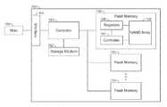
- FIG. 1is a block diagram illustrating components of a data storage system according to one aspect of the subject technology.
- FIG. 2is a diagram illustrating an exemplary graph diagram of four possible cell V T distributions and complimentary program verify levels for a group of memory cells in a multi-level cell flash memory according to one aspect of the subject technology.
- FIG. 3is a graph diagram illustrating an exemplary threshold voltage evolution of a 2-bit MLC NAND flash memory cell with programming and erase conditions chosen apriori at beginning of life according to one aspect of the subject technology.
- FIG. 4is a graph diagram illustrating program and erase time evolutions according to one aspect of the subject technology.
- FIG. 5is a graph diagram illustrating the V T distribution width evolutions according to one aspect of the subject technology.
- FIG. 6is a graph diagram illustrating a single-phase erase procedure according to one aspect of the subject technology.
- FIG. 7is a flowchart illustrating a process for determining adjusted programming and/or erase parameters according to one aspect of the subject technology.
- FIGS. 8A to 8Care graph diagrams illustrating measured programming and erase time evolution over P/E cycling for a NAND flash memory device according to one aspect of the subject technology.
- FIG. 9is a flowchart illustrating a process for obtaining optimal BOL condition values for P/E parameters to be implemented on a NAND memory block according to one aspect of the subject technology.
- FIG. 10is a graph diagram illustrating an exemplary T PROG evolution over P/E cycling according to one aspect of the subject technology.
- memory cellsare grouped in strings, with each string consisting of a set of transistors connected in series between a drain select transistor, connected to a bit line of the memory block, and a source select transistor, connected to a reference voltage distribution line.
- Each memory cellconsists of a floating-gate MOS transistor.
- F-NFowler-Nordheim
- Bitsare stored by trapping charge on the floating gate (an electrically isolated conductor) which stores a logic value defined by the threshold voltage of the cell (read threshold) commensurate with the electric charge stored.
- the electrons in the floating gateare removed by quantum mechanical tunneling (a tunnel current) from the floating gate to, for example, the source and/or substrate.
- flash memoryAs flash memory is cycled (that is, programmed and erased repeatedly), its physical qualities change. For example, the repeated placement and removal of electrons to and from the floating gate during programming and erase operations, respectively, causes some excess electrons to be trapped in the device. Also, when one or multiple cells are programmed, adjacent cells may experience an unexpected and undesired charge injection to their floating gates, thus leading to corruption of data stored therein. For instance, electrons may leak into neighboring cells after prolonged stress due to the voltages at the gates of neighboring cells. The threshold voltages of these memory cells may eventually take values that are different (higher or lower) than expected values, causing errors when the data is read.
- the damage donebecomes a function of the field strength (voltage) and duration; that is, programming the flash memory to high threshold voltage conditions increases the rate of damage arising from both program and erase processes because it requires longer duration and/or higher applied fields. For instance, adding enough electrons can change a cell from an erased state to a programmed state.
- the subject technologyprovides a system and process for use in memory cell architectures that dynamically adjusts program and erase conditions to reduce bit error rate (BER) and variation in device performance, and to achieve a higher number of cycles the device can undergo, thereby improving the reliability and endurance of flash memory, making it suitable for enterprise applications.
- BERbit error rate
- FIG. 1is a block diagram illustrating components of a data storage system according to one aspect of the subject technology.
- data storage system 100(for example, a solid state drive) includes data storage controller 101 , storage medium 102 , and flash memory 103 .
- Controller 101may use storage medium 102 for temporary storage of data and information used to manage data storage system 100 .
- Controller 101may include several internal components (not shown) such as a read-only memory, a flash component interface (for example, a multiplexer to manage instruction and data transport along a serial connection to flash memory 103 ), an I/O interface, error correction circuitry, and the like.
- all of these elements of controller 101may be integrated into a single chip. In other aspects, these elements may be separated on their own PC board.
- Controller 101may also include a processor that may be configured to execute code or instructions to perform the operations and functionality described herein, manage request flow and address mappings, and to perform calculations and generate commands.
- the processor of controller 101is configured to monitor and/or control the operation of the components in controller 101 .
- the processormay be a general-purpose microprocessor, a microcontroller, a digital signal processor (DSP), an application specific integrated circuit (ASIC), a field programmable gate array (FPGA), a programmable logic device (PLD), a state machine, gated logic, discrete hardware components, or a combination of the foregoing.
- DSPdigital signal processor
- ASICapplication specific integrated circuit
- FPGAfield programmable gate array
- PLDprogrammable logic device
- One or more sequences of instructionsmay be stored as firmware on ROM within controller 101 and/or its processor.
- One or more sequences of instructionsmay be software stored and read from storage medium 102 , flash memory 103 , or received from host device 104 (for example, via host interface 105 ).
- ROM, storage medium 102 , and flash memory 103represent examples of machine or computer readable media on which instructions/code executable by controller 101 and/or its processor may be stored.
- Machine and/or computer readable mediamay generally refer to any medium or media used to provide instructions to controller 101 and/or its processor, including volatile media, such as dynamic memory used for storage media 102 or for buffers within controller 101 , and non-volatile media, such as electronic media, optical media, and magnetic media.
- controller 101is configured to store data received from a host device 104 in flash memory 103 in response to a write command from host device 104 . Controller 101 is further configured to read data stored in flash memory 103 and to transfer the read data to host device 104 in response to a read command from host device 104 . As will be described in more detail below, controller 101 may be configured to, as the number of P/E cycles increases, determine and/or adjust program and/or erase conditions as a function of one or more circuit characteristics associated with flash memory 103 .
- the subject technologymay increase the number of P/E operations that may be performed on memory cells within flash memory 103 in a particular application environment, and increase the endurance of the cells compared to the same application environment operating without the ability to dynamically adjust these conditions.
- Host device 104represents any device configured to be coupled to data storage system 100 and to store data in data storage system 100 .
- Host device 104may be a computing system such as a personal computer, a server, a workstation, a laptop computer, PDA, smart phone, and the like.
- host device 104may be an electronic device such as a digital camera, a digital audio player, a digital video recorder, and the like.
- storage medium 102represents volatile memory used to temporarily store data and information used to manage data storage system 100 .
- storage medium 102is random access memory (RAM) such as double data rate (DDR) RAM.
- RAMrandom access memory
- DDRdouble data rate
- Other types of RAMalso may be used to implement storage medium 102 .
- Memory 102may be implemented using a single RAM module or multiple RAM modules. While storage medium 102 is depicted as being distinct from controller 101 , those skilled in the art will recognize that storage medium 102 may be incorporated into controller 101 without departing from the scope of the subject technology.
- storage medium 102may be a non-volatile memory such as a magnetic disk, flash memory, peripheral SSD, and the like.
- data storage system 100may also include host interface 105 .
- Host interface 105is configured to be operably coupled to host device 104 (for example, by wired or wireless connection), to receive data from host device 104 and to send data to host device 104 .
- Host interface 105may include electrical and/or physical connections, and or wireless connection, for operably coupling host device 104 to controller 101 (for example, via the I/O interface of controller 101 ).
- Host interface 105is configured to communicate data, addresses, and control signals between host device 104 and controller 101 .
- the I/O interface of controller 101may include and/or be combined with host interface 105 .
- Host interface 105may be configured to implement a standard interface, such as Serial-Attached SCSI (SAS), Fiber Channel interface, PCI Express (PCIe), SATA, USB, and the like. Host interface 105 may be configured to implement only one interface. Alternatively, host interface 105 (and/or the I/O interface of controller 101 ) may be configured to implement multiple interfaces, which may be individually selectable using a configuration parameter selected by a user or programmed at the time of assembly. Host interface 105 may include one or more buffers for buffering transmissions between host device 104 and controller 101 .
- SASSerial-Attached SCSI
- PCIePCI Express
- SATASerial-Attached SCSI
- USBUniversal Serial-Attached SCSI
- Host interface 105may be configured to implement only one interface. Alternatively, host interface 105 (and/or the I/O interface of controller 101 ) may be configured to implement multiple interfaces, which may be individually selectable using a configuration parameter
- Flash memory 103represents a non-volatile memory device for storing data.
- flash memory 103includes, for example, a NAND flash memory.
- Flash memory 103may include a single flash memory device or chip, or, as depicted by FIG. 1 , may include multiple flash memory devices or chips arranged in multiple channels. Flash memory 103 is not limited to any particular capacity or configuration. For example, the number of physical blocks, the number of physical pages per physical block, the number of sectors per physical page, and the size of the sectors may vary within the scope of the subject technology.
- Flash memorymay have a standard interface specification. This standard ensures that chips from multiple manufacturers can be used interchangeably (at least to a large degree).
- the interfacehides the inner working of the flash memory and returns only internally detected bit values for data.
- the interface of flash memory 103is used to access one or more internal registers 106 and an internal flash controller 107 for communication by external devices.
- registers 106may include address, command, and/or data registers, which internally retrieve and output the necessary data to and from a NAND memory cell array 108 .
- a data registermay include data to be stored in memory array 108 , or data after a fetch from memory array 108 , and may also be used for temporary data storage and/or act like a buffer.
- An address registermay store the memory address from which data will be fetched to host 104 or the address to which data will be sent and stored.
- a command registeris included to control parity, interrupt control, and the like.
- internal flash controller 107is accessible via a control register to control the general behavior of flash memory 103 .
- Internal flash controller 107 and/or the control registermay control the number of stop bits, word length, receiver clock source, and may also control switching the addressing mode, paging control, coprocessor control, and the like.
- registers 106may also include a test register.
- the test registermay be accessed by specific addresses and/or data combinations provided at the interface of flash memory 103 (for example, by specialized software provided by the manufacturer to perform various tests on the internal components of the flash memory).
- the test registermay be used to access and/or modify other internal registers, for example the command and/or control registers.
- test modes accessible via the test registermay be used to input or modify certain programming parameters of flash memory 103 (for example, voltage levels applied to memory cells) to dynamically vary how data is programmed to and/or erased from the memory cells of memory arrays 108 .
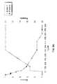
- FIG. 2is a diagram illustrating an exemplary graph diagram of four possible cell V T distributions and corresponding program verify levels for a group of memory cells in a multi-level cell flash memory according to one aspect of the subject technology.
- an MLC NAND cellis capable of storing four states (amounts of charge) per cell, yielding two logical bits of information per cell: the Most Significant Bit (MSB) and the Least Significant Bit (LSB). These two bits may make up corresponding MSB and LSB pages of a memory block.
- MSBMost Significant Bit
- LSBLeast Significant Bit
- a NAND memory blockis programmed one page at a time using an Incremental Step Pulse Program (ISSP) and erased using a similar Incremental Step Pulse Erase Erase (ISPE).
- ISPP and/or ISPEmay be performed by flash controller 107 in response to one or more commands received from controller 101 .
- the memory cells that are to be programmed by ISPPmay be selected at the bit line.
- a “page operation”may be performed by applying a voltage at the gates of each cell in the memory page.
- a corresponding selection at the bit linescreates a voltage potential in the selected group of memory cells where the LSB is selected to be different (for example, binary 10 or 00) than the erased L0 distribution state 201 (for example, binary 11).
- ISPPincreases 202 the threshold voltage V T 203 of the selected group of cells to create LSB distribution 204 .
- ISPPis applied to create an L1 distribution 205 from the erased L0 distribution 201 (for example, binary 01), or, an L2 distribution 206 (for example, binary 00) or L3 distribution 207 (for example, binary 10) from the previously programmed LSB distribution 204 .
- L0 distribution 201for example, binary 01
- L2 distribution 206for example, binary 00
- L3 distribution 207for example, binary 10
- all of the above distributionsare created from L0 distribution 201 by applying a series of ISPP voltage pulses to the memory cells of the page which is being programmed.
- the ISPPincludes a series of voltage pulses that are applied in a step pattern with the amplitude of each pulse incrementally increased with increasing pulse number, starting from a certain starting magnitude.
- flash controller 107 of flash memory 103may perform a programming verification (sensing) operation in between each step. To verify that a cell has been successfully programmed, controller 107 applies a program verify voltage 208 in an attempt to measure the voltage of the cell. In some aspects, if the threshold voltage of a cell in the memory page is detected above a certain program verify level, flash controller 107 may stop further programming of that single cell by setting it to a program inhibit state.
- LSB and MSB programmingmay use different values of ISPP starting magnitude and/or ISPP step magnitude. Accordingly, different ISPP step and/or starting magnitudes may be used during the MSB programming of L1 distribution 205 than in the programming of L2 distribution 206 and/or L3 distribution 207 . This is because programming to a higher V T level may require the application of a higher programming voltage potential. It has been found that higher programming pulse magnitudes generally result in faster programming, and smaller ISPP step magnitudes and/or narrower pulse widths generally result in narrower final V T distributions (for example, a distribution of cells programmed to the same V T distribution having a smaller standard deviation).
- these parameter valuesmay be stored in one or more lookup tables in storage medium 102 and accessed by controller 101 to use in conjunction with generating commands.
- Controller 101may be configured to communicate with and provide the commands to flash memory 103 via registers 106 (for example, the test register) and/or flash controller 107 to modify the ISPP and/or ISPE parameters of flash memory 103 (for example, nominal parameters set by the chip manufacturer) to vary the V T distributions at run-time.
- these parameterscan be dynamically determined and/or adjusted at run-time as a function of various circuit characteristics (for example, P/E cycles, programming and/or erase time, retention time, BER, temperature, memory block address, memory page address, and the like) and/or in response to commands received from host 104 via host interface 105 .
- circuit characteristicsfor example, P/E cycles, programming and/or erase time, retention time, BER, temperature, memory block address, memory page address, and the like
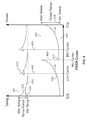
- FIG. 3is a graph diagram illustrating an exemplary threshold voltage evolution of a 2-bit MLC NAND flash memory cell with programming and erase conditions chosen apriori at beginning of life according to one aspect of the subject technology.
- the topmost rowrepresents the four possible distributions of each programming state in a group of memory cells at beginning of life (BOL).
- the respective programming distributions of L0 distribution 201 , L1 distribution 205 , L2 distribution 206 , and L3 distribution 207are shown along a voltage threshold continuum 301 .
- the middle row of FIG. 3depicts an exemplary progression of the programming distributions after repeated P/E cycling.
- the buildup of electrons trapped in the memory cellshas caused some cells be programmed to higher voltage thresholds (increasing the standard deviation of the distribution at a higher V T ).
- This shift 306 in voltage thresholdsmay eventually cause the right edges of the V T distributions to reach the higher adjacent read levels.
- the bottom rowdepicts an exemplary result of an extended retention time on the memory cells. After a number of P/E cycles and an extended retention time memory cells have lost electrons, causing the voltage thresholds of the cells to decrease.
- This shift 308may eventually cause the left edges of the V T distributions to reach the lower adjacent read levels. The bigger the number of P/E operations performed on the memory cells and the longer the retention time, the more extreme the decrease in the voltage thresholds of the memory cells. If the read levels remain fixed, the V T distributions that have crossed 309 the next lower read level may cause significant errors.
- the edges of each of the distributionsare suitably spaced from adjacent read levels.
- spacingcan be altered by setting program verify voltages 305 (for example, PV 1 , PV 2 , and/or PV 3 ) during the verification operation sufficiently higher than a lower read level, but sufficiently low enough to prevent even those cells in the distribution having the highest V T (largest deviation) from crossing the adjacent higher read level.
- program verify voltages 305for example, PV 1 , PV 2 , and/or PV 3
- RL 1 voltage 302will cause cells in L0 distribution 201 to conduct
- RL 2 voltage 303will cause cells in L1 distribution 205 to conduct
- RL 3 voltage 304will cause cells in L2 distribution to conduct, and so on.
- RL 3 voltage 304will not cause any cells in L3 distribution 207 to conduct, thereby generating a binary x0 in the LSB (see FIG. 2 ) for those cells.
- N distributionsthere will be N ⁇ 1 read levels. In the depicted example, there are four distributions (of V T states) and three read levels. Those skilled in the art will recognize that there may be eight, sixteen, or more distributions without departing from the scope of the subject technology.
- read levelsare programmed to remain static to accommodate both higher and lower V T distribution shifts.
- Controller 101is configured to, as BER increases, determine and dynamically adjust the ISPP and/or ISPE parameters to correct the standard deviations of the distributions to reduce the risk of the V T distributions crossing their adjacent read levels, and to prolong the endurance of the memory cells.
- controller 101may progressively reduce the values of the input parameters to ISPP (for example, starting magnitude voltages, steps, and pulse widths) for both LSB and MSB programming.
- the parametersmay also be adjusted while keeping the programming time within a certain predetermined range.
- the parametersmay represent a voltage level or a function thereof, however, one skilled in the art will recognize that the parameters may represent, for example, an electric current, electrical resistance, slope thereof, and the like.
- FIG. 4is a graph diagram illustrating program and erase time evolutions according to one aspect of the subject technology.
- a write operationwill take a maximum programming duration 401 .
- the programming time 402will progressively decrease towards a minimum programming duration 403 , producing a programming duration range 404 over a range of P/E cycles.
- an erase operationwill take a minimum erase duration 405 .
- erase time 406will progressively increase toward maximum erase duration 407 , producing an erase duration range 408 over a range of cycles.
- Controller 101is configured to determine parameters for ISPP and ISPE as a function of various circuit characteristics and send commands to flash memory 103 to dynamically reset the programming and/or erase conditions and correct the distributions.
- parametersmay include starting magnitude, step magnitude, pulse width, and the like.
- parametersare determined as a function of certain circuit characteristics, including, for instance, the current number of P/E cycles, a value based on the number or range of P/E cycles, programming and/or erase time, retention time, memory block address, memory page address, or a temperature (for example, the die temperature of flash memory 103 ).
- controller 101may be programmed to check, determine, and/or adjust the program and/or erase conditions on a trigger event 409 .
- trigger event 409may be a number or range of P/E cycles (for example, every 1,000 cycles after an initial trigger at 500 cycles) or a set duration (for example, programming time 402 , erase time 406 , or the age of the SSD).
- controller 101may be configured to monitor a duration and to invoke a trigger event when the monitored condition (for example, programming time 402 or erase time 406 ) exceeds a predetermined limit (for example, minimum programming duration 403 , maximum programming duration 401 , minimum erase duration 405 , maximum erase duration 407 , or the like).
- controller 101may be configured to progressively set the ISPP starting pulse voltage level lower at each successive trigger event so that revised maximum duration 410 does not cause the BER to increase beyond an acceptable predetermined limit (for example, maintain standard deviation 501 below maximum deviation 503 and/or sufficiently below the adjacent higher read level).
- controller 101may access one or more trigger lookup tables stored on storage medium 102 to determine when a trigger should take place.
- the one or more lookup tablesmay provide trigger information based on a number of P/E cycles or range of cycles and/or a duration as previously described.
- adjustments to parameter valuesare planned as the drive ages via one or more parameter lookup tables, which may be indexed by cycle and/or timestamp. Once a trigger event is met (for example, “BOL”, “low cycles”, “mid cycles”, “EOL”), controller 101 accesses the one or more parameter lookup tables to facilitate adjustment of the ISPP and/or ISPE parameters.
- the number or range usedcan either be an average across all memory blocks in flash memory 103 or based on individual memory block information.
- a dynamic adjustmentcan be performed on all flash memories 103 in storage system 100 at once, on individual chips, on individual blocks, or on individual pages.
- One or more trigger eventsmay optionally be embedded in the hardware of controller 101 or included in programming code which is executed on controller 101 .
- controller 101may be configured to invoke trigger event 409 when programming duration 402 reaches minimum programming duration 403 .
- trigger event 409the ISPP parameters are reduced so that the distributions are more narrowly programmed and retain sufficient spacing from adjacent read level voltages.
- controller 101may be configured to program flash memory 103 so that, once some of the cells in a distribution (for example, L1 distribution 205 ) are beyond a program verify voltage (for example, program verify voltage 305 ), the ISPP parameters are adjusted so that further programming of the page and/or block using ISPP does not cause cells in the distribution having larger magnitudes (for example, having excess electrons due to degradation of the cells) to become too close to the adjacent higher read level voltage (for example, voltage 303 ), thereby narrowing the standard deviation of the distribution.
- a program verify voltagefor example, program verify voltage 305
- controller 101may reset the ISPP parameters as a function of programming duration 402 to maintain programming duration 402 within predefined limits. For example, if controller 101 determines that maximum programming duration 401 would render an unacceptable BER (for example, after extended retention), controller 101 may determine and adjust the ISPP parameters (for example, to higher levels) to modify programming duration 402 such that its maximum limit is maintained or lowered to a revised maximum duration 410 . Likewise, if minimum programming duration 403 would render an unacceptable BER (for example, after excessive cycling), controller 101 may determine and adjust the ISPP parameters (for example, to lower levels) to modify programming duration 402 such that its minimum limit is maintained or raised to a revised minimum programming duration.
- the maximum acceptable BERmay be determined by a maximum number of bits correctable by ECC.
- controller 101uses ECC to accommodate a certain level of BER.
- controller 101may be configured to receive a page and/or block of data and process that data using ECC (for example, an ECC algorithm) to determine BER and then determine whether that BER is within a predetermined acceptable limit. If BER is too high then controller 101 may determine that a V T distribution has shifted to an unacceptable level (for example, too high).
- Controller 101may be configured to adjust the program and/or erase conditions in accordance with the previously described procedure based on the increase and/or decrease in BER (for example, at a specific value or error slope/acceleration thereof).
- Adjustment of the ISPP parametersmay maintain standard deviation 501 within deviation range 504 , and/or to move standard deviation 501 as close as possible to minimum deviation 502 , at a revised minimum deviation 505 .
- revised minimum deviation 505may be the result of physical degradation of the memory device and/or revised programming duration 410 (see FIG. 4 ).
- controller 101determines ISPP parameters to correct standard deviation 501 (for example, narrow and/or shift the distribution).
- controller 101may be configured to monitor BER (for example, periodically or on a read or write operation) and, if it determines that one or more of the programmed V T distributions are outside the deviation limit (for example, determines a distribution is at maximum deviation 503 by receiving a high BER), further determine and adjust the ISPP parameters.
- Controller 101may determine and adjust the ISPP parameters such that the next programming operation performed will create a V T distribution of memory cells having a standard deviation at or near minimum deviation 502 .
- the ISPP parametersmay further be set as a function of ISPP programming time 402 and/or erase time 406 .
- FIG. 6is a graph diagram illustrating a single-phase erase procedure according to one aspect of the subject technology.
- flash memory 103is instructed by controller 101 to perform an Incremental Step Pulse Erase (ISPE) whereby all of the programmed levels, for example, L1 distribution 205 , L2 distribution 206 , and L3 distribution 207 , are returned 601 to the L0 distribution state 201 .
- ISPEIncremental Step Pulse Erase
- controller 101is configured to issue commands to flash memory 103 to apply a series of voltage pulses to the memory cells which are being erased.
- the amplitude polarityis reversed (from ISPP) to remove electrons from the floating gates of the memory cells.
- the ISPEincludes a series of voltage pulses that are applied in a step pattern with the amplitude of each pulse incrementally increased with increasing pulse number, starting from a starting magnitude.
- ISPEcan be performed in a similar manner to ISPP, including, for example, adjustment of the pulse parameters, conditions, verification, and the like.
- ISPEis applied to all of the cells of a memory block at once (for example, 64 or 128 or more pages).
- Controller 101may be configured to determine and/or adjust one or more ISPE parameters, including, for example, starting magnitude, step magnitude, the number of steps, the width of the erase pulses, current, slope, and the like.
- the step between the first and the second pulsescan, sometimes, be defined separately from subsequent steps.
- an erase operationmay be followed by a very mild programming step (controlled by its own ISPP starting magnitude and step), to render the final erased distribution narrower (for example, to reset L0 distribution 201 ). Similar to ISPP, those skilled in the art will recognize how to select the appropriate parameters as input to an ISPE to achieve an erased distribution (for example, L0) from a selected higher distribution (for example, L1, L2, or L3).
- erase duration range 408 of memory erase time 405may be chosen to be relatively small to increase the overall performance of the system without sacrificing endurance of flash memory 103 .
- a range of acceptable erase durationsmay be stored in one or more lookup tables on storage medium 102 .
- controller 101may also be configured to monitor the duration of the ISPE and, on sensing memory erase time 406 has reached a maximum erase duration 407 , send commands to flash memory 103 to modify the ISPE parameters such that erase time 406 is reduced toward minimum erase duration 405 or a revised minimum erase duration 411 .
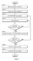
- FIG. 7is a flowchart illustrating a process for determining adjusted programming and/or erase parameters according to one aspect of the subject technology.
- a trigger eventfor example, trigger event 409 , described previously
- storage system 100including controller 101 , begins normal drive operation.
- controller 101monitors memory operations (for example, the current P/E cycle count and/or programming or erase duration), and waits for the trigger event.
- step S 704controller 101 optionally retrieves one or more condition values to be used in the calculation of the parameter to be adjusted (for example, maximum programming duration 403 , minimum programming duration 401 , programming range 404 , minimum erase duration 405 , maximum erase duration 407 , erase duration range 408 , and/or the like).
- the one or more condition valuesmay optionally be embedded in the hardware of controller 101 or included in programming code which is executed on controller 101 .
- step S 704may be omitted and/or the condition value previously retrieved in an antecedent step.
- controller 101begins to adjust the current ISPP and/or ISPE parameters for the next programming and/or erase cycle.
- Controller 101may determine one or more new parameters (for example, starting magnitude voltages, steps, and pulse widths) as a function of program and/or erase cycles.
- controller 101determines new parameter(s) as a function of stored values, for example, values located in a lookup table.
- controller 101indexes the lookup table by one or more present characteristics (for example, P/E cycle, temperature, a duration, and the like) to retrieve the parameter(s).
- controller 101may be optionally configured to adjust the parameter(s) while checking to make sure the operating conditions (for example, programming duration 402 ) are within the designated limits/range. For example, controller 101 may perform a calculation of programming duration 402 in conjunction with a calculation of the parameters such that programming duration 402 remains within a programming range 404 . This may also include determining (for example, calculating) the parameters such that programming duration 402 is reset to maximum programming duration 401 or revised maximum duration 410 . Controller 101 may store the current parameter(s) (for example, in storage medium 102 ) and adjusts the parameter(s) based on desired operating conditions.
- the operating conditionsfor example, programming duration 402
- controller 101may perform a calculation of programming duration 402 in conjunction with a calculation of the parameters such that programming duration 402 remains within a programming range 404 . This may also include determining (for example, calculating) the parameters such that programming duration 402 is reset to maximum programming duration 401 or revised maximum duration 410 . Controller 101 may store the current parameter(s) (for example
- controller 101may first decrease the starting magnitude of the first ISPP pulse and then maintain and/or reduce the step increment and/or pulse width to maintain an upper range of the distribution at a sufficient distance from the next higher read level (for example, after a predetermined number of cycles).
- controller 101may be configured to increase one or more parameters (for example, starting magnitude) to reduce programming time 402 (for example, after extended retention time).
- a reduction in programming time 402may be a result of increasing the parameter(s) to reduce standard deviation 501 .
- the increasemay be selected and/or determined based on programming time 402 which results in reducing standard deviation 501 .
- controller 101may readjust the parameter(s) in a closed loop by returning to step S 705 .
- the limit or programming time 402may be determined by a verification operation undertaken by flash memory 103 .
- flash memory 103may cease programming the distribution when all the cells are at (or above) the program verify level 305 (see FIG. 3 ).
- step S 705once the distribution has been verified, further adjustment of the parameter(s) will cease, thereby determining programming duration 402 .
- the verificationis undertaken by controller 101 during the calculation of the parameter(s) before any command is sent to flash memory 103 .
- controller 101when adjusting an erase condition, controller 101 is configured to increase one or more parameters (for example, starting magnitude) to reduce erase time 406 .
- controller 101may check that the newly adjusted parameter(s) does not cause erase time 406 to fall out of range 408 (for example, exceed maximum erase duration 405 ).
- erase time 406may be determined by a verification operation, that is, flash memory 103 will undertake program verification operations and cease erase when all the cells are at (or below) an erase verify level.
- step S 707once L0 distribution 201 has been verified, further adjustment of the parameter will cease, thereby modifying erase duration 406 such that its minimum limit is maintained or raised to a revised minimum duration 411 (see FIG. 4 ).
- FIGS. 8A to 8Care graph diagrams illustrating measured programming and erase time evolution over P/E cycling for a NAND flash memory device according to one aspect of the subject technology.
- the subject technologywas applied to a NAND flash memory device to maintain an acceptable BER while cycling the device above the manufacturer specified limit of 30 k P/E cycles.
- FIG. 8Ais a graph diagram illustrating an evolution of starting program pulse voltage levels and starting erase pulse voltage levels that were applied.
- An ISPP starting pulse voltage register, PRSTARTUwas used to specify the starting program pulse voltage level as a function of P/E cycles.
- An ISPE starting erase pulse voltage level register, ERASESTwas used to specify the starting erase pulse voltage level as a function of P/E cycles. As depicted in FIG.
- the subject technologyadjusts the ISPP starting program pulse voltage level and the ISPE starting erase pulse voltage level as a function of P/E cycles in order to keep the values of T PROG and T ERASE within their respective allowed limits.
- the controllerperiodically performs a check to see whether T PROG and T ERASE need to be adjusted at specific P/E cycles counts: 1 k, 2 k, 3 k, 4 k, 5 k, 10 k, 20 k, and the like.
- FIG. 8Billustrates measured programming time as a function of P/E cycles.
- Programming time T PROGis graphed corresponding to the adjustment of ISPP starting program pulse voltage level.
- a minimum and maximum allowed T PROGwere chosen as 1.5 ms and 1.6 ms, respectively.
- T PROG valuewas measured at specific P/E cycles, and, as collectively depicted by FIGS. 8A and 8B , once T PROG falls below a minimum of 1.5 ms, starting program pulse voltage is reduced until T PROG is within allowed limits.
- FIG. 8Cillustrates the measured evolution of the number of erase pulses as a function of P/E cycles.
- the number of erase pulses, N ERASEis graphed corresponding to the adjustment of starting erase pulse level (depicted in FIG. 8A ).
- Erase timefor example, between 750 ⁇ s and 1 ms per erase pulse
- T ERASEis proportional to the number of erase pulses, N ERASE .
- the minimum and maximum allowed number of erase pulseswere chosen as 14 and 15, respectively.
- the number of erase pulses, N ERASEwas also measured at the depicted P/E cycles, and once N ERASE was above a maximum of 15, starting erase pulse voltage was increased until N ERASE was within allowed limits.
- the subject technologymay achieve 60 k P/E cycles while keeping the T PROG and T ERASE within their limits and maintaining a BER level lower than that originally specified by the device manufacturer at 30 k P/E cycles.
- FIG. 9is a flowchart illustrating a process for obtaining optimal ISPP and/or ISPE parameters to be implemented on a NAND memory block according to one aspect of the subject technology.
- step S 901the desired ranges and/or limits of programming time 402 (T PROG ), erase time 406 (T ERASE ), and standard deviation 501 are identified and stored in storage medium 102 .
- controller 101collects nominal T PROG , T ERASE , and V T distribution data for a block in flash memory 103 as a function of ISPP and/or ISPE parameters.
- a parameter set for ISPP and/or ISPEis determined based on the nominal data collected and, in step S 903 , the parameter set is fixed and controller 101 provides flash memory 103 with the parameter set for ISPP and/or ISPE operations.
- the parameter setmay also be stored on storage medium 102 and/or associated with a specific block.
- the parameter setmay be stored in one or more parameter lookup tables and indexed by P/E cycle or other operating and/or circuit characteristic herein described. Controller 101 may access the lookup table during runtime to retrieve the parameter(s) and to adjust the operating conditions.
- step S 904a memory block of flash memory 103 is then selected and cycled N times until T PROG reaches minimum programming duration 403 , T ERASE reaches maximum erase duration 403 , and/or standard deviation 501 reaches maximum deviation width 503 (see FIGS. 4 and 5 ).
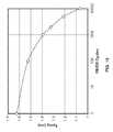
- FIG. 10is a graph diagram illustrating an exemplary T PROG evolution over P/E cycling according to one aspect of the subject technology.
- step S 905after the block has been cycled for N times, a new satisfactory set of ISPP and/or ISPE parameters is identified and selected. In this regard, the new parameters may be manually selected to achieve an optimal T PROG , T ERASE , and/or standard deviation.
- the new parametersare selected to allow further cycling of flash memory 103 in view of the V T degradation occurring as a result of step S 904 .
- the parametersmay also be, at least in part, determined as a function of circuit characteristics (for example, P/E count, die temperature, current increase, memory block address, memory page address and the like).
- controller 101provides flash memory 103 with the new parameter set for further ISPP and/or ISPE operations.
- Steps S 904 and S 905may then be repeated until a desired number of P/E cycles is reached.
- Each resulting parameter set from repeated step S 905may be included in the one or more parameter lookup tables described in step S 903 .
- step S 906the memory block is put through a retention bake.
- one or more post-bake readsmay then be undertaken to make sure that the maximum number of cycles reached does not result in excessive BER.
- the subject technologyBy dynamically adjusting program and erase conditions, for the same level of maximum acceptable BER and the same expected retention time, the subject technology allows a drive to achieve a higher number of cycles than a drive without the subject technology. Similarly, for the same number of cycles and the same expected retention time the subject technology allows the SSD to achieve a lower BER, markedly improving SSD performance throughout the lifetime of the drive.
- a processor configured to monitor and control an operation or a componentmay also mean that the processor is programmed to monitor and control the operation or the processor being operable to monitor and control the operation.
- a processor configured to execute codecan be construed as a processor programmed to execute code or operable to execute code.
- a phrase such as an “aspect”does not imply that such aspect is essential to the subject technology or that such aspect applies to all configurations of the subject technology.
- a disclosure relating to an aspectmay apply to all configurations, or one or more configurations.
- An aspectmay provide one or more examples.
- a phrase such as an aspectmay refer to one or more aspects and vice versa.
- a phrase such as an “embodiment”does not imply that such embodiment is essential to the subject technology or that such embodiment applies to all configurations of the subject technology.
- a disclosure relating to an embodimentmay apply to all embodiments, or one or more embodiments.
- An embodimentmay provide one or more examples.
- a phrase such as an “embodiment”may refer to one or more embodiments and vice versa.
- a phrase such as a “configuration”does not imply that such configuration is essential to the subject technology or that such configuration applies to all configurations of the subject technology.
- a disclosure relating to a configurationmay apply to all configurations, or one or more configurations.
- a configurationmay provide one or more examples.
- a phrase such as a “configuration”may refer to one or more configurations and vice versa.
Landscapes
- Engineering & Computer Science (AREA)
- Theoretical Computer Science (AREA)
- Physics & Mathematics (AREA)
- General Engineering & Computer Science (AREA)
- General Physics & Mathematics (AREA)
- Quality & Reliability (AREA)
- Human Computer Interaction (AREA)
- Health & Medical Sciences (AREA)
- Biomedical Technology (AREA)
- Read Only Memory (AREA)
- Techniques For Improving Reliability Of Storages (AREA)
Abstract
Description
Claims (25)
Priority Applications (3)
| Application Number | Priority Date | Filing Date | Title |
|---|---|---|---|
| US13/177,518US8737141B2 (en) | 2010-07-07 | 2011-07-06 | Apparatus and method for determining an operating condition of a memory cell based on cycle information |
| US14/252,746US9389938B2 (en) | 2010-07-07 | 2014-04-14 | Apparatus and method for determining an operating condition of a memory cell based on cycle information |
| US15/207,414US10613781B2 (en) | 2010-07-07 | 2016-07-11 | Apparatus and method for determining an operating condition of a memory cell based on cycle information |
Applications Claiming Priority (2)
| Application Number | Priority Date | Filing Date | Title |
|---|---|---|---|
| US36227210P | 2010-07-07 | 2010-07-07 | |
| US13/177,518US8737141B2 (en) | 2010-07-07 | 2011-07-06 | Apparatus and method for determining an operating condition of a memory cell based on cycle information |
Related Child Applications (1)
| Application Number | Title | Priority Date | Filing Date |
|---|---|---|---|
| US14/252,746DivisionUS9389938B2 (en) | 2010-07-07 | 2014-04-14 | Apparatus and method for determining an operating condition of a memory cell based on cycle information |
Publications (2)
| Publication Number | Publication Date |
|---|---|
| US20120239858A1 US20120239858A1 (en) | 2012-09-20 |
| US8737141B2true US8737141B2 (en) | 2014-05-27 |
Family
ID=46829404
Family Applications (3)
| Application Number | Title | Priority Date | Filing Date |
|---|---|---|---|
| US13/177,518ActiveUS8737141B2 (en) | 2010-07-07 | 2011-07-06 | Apparatus and method for determining an operating condition of a memory cell based on cycle information |
| US14/252,746Expired - Fee RelatedUS9389938B2 (en) | 2010-07-07 | 2014-04-14 | Apparatus and method for determining an operating condition of a memory cell based on cycle information |
| US15/207,414Active2032-01-22US10613781B2 (en) | 2010-07-07 | 2016-07-11 | Apparatus and method for determining an operating condition of a memory cell based on cycle information |
Family Applications After (2)
| Application Number | Title | Priority Date | Filing Date |
|---|---|---|---|
| US14/252,746Expired - Fee RelatedUS9389938B2 (en) | 2010-07-07 | 2014-04-14 | Apparatus and method for determining an operating condition of a memory cell based on cycle information |
| US15/207,414Active2032-01-22US10613781B2 (en) | 2010-07-07 | 2016-07-11 | Apparatus and method for determining an operating condition of a memory cell based on cycle information |
Country Status (1)
| Country | Link |
|---|---|
| US (3) | US8737141B2 (en) |
Cited By (17)
| Publication number | Priority date | Publication date | Assignee | Title |
|---|---|---|---|---|
| US20130185612A1 (en)* | 2012-01-18 | 2013-07-18 | Samsung Electronics Co., Ltd. | Flash memory system and read method of flash memory system |
| US20160180951A1 (en)* | 2014-12-22 | 2016-06-23 | Sandisk Technologies Inc. | Measuring memory wear and data retention individually based on cell voltage distributions |
| US9377962B2 (en)* | 2012-02-23 | 2016-06-28 | Hgst Technologies Santa Ana, Inc. | Determining bias information for offsetting operating variations in memory cells |
| US9583207B2 (en)* | 2015-02-10 | 2017-02-28 | Sandisk Technologies Llc | Adaptive data shaping in nonvolatile memory |
| US20170140827A1 (en)* | 2014-02-14 | 2017-05-18 | Sony Semiconductor Solutions Corporation | Memory device with variable trim parameters |
| US9799405B1 (en) | 2015-07-29 | 2017-10-24 | Ip Gem Group, Llc | Nonvolatile memory system with read circuit for performing reads using threshold voltage shift read instruction |
| US9813080B1 (en) | 2013-03-05 | 2017-11-07 | Microsemi Solutions (U.S.), Inc. | Layer specific LDPC decoder |
| US9886214B2 (en) | 2015-12-11 | 2018-02-06 | Ip Gem Group, Llc | Nonvolatile memory system with erase suspend circuit and method for erase suspend management |
| US9892794B2 (en) | 2016-01-04 | 2018-02-13 | Ip Gem Group, Llc | Method and apparatus with program suspend using test mode |
| US9899092B2 (en) | 2016-01-27 | 2018-02-20 | Ip Gem Group, Llc | Nonvolatile memory system with program step manager and method for program step management |
| US10157677B2 (en) | 2016-07-28 | 2018-12-18 | Ip Gem Group, Llc | Background reference positioning and local reference positioning using threshold voltage shift read |
| US10230396B1 (en) | 2013-03-05 | 2019-03-12 | Microsemi Solutions (Us), Inc. | Method and apparatus for layer-specific LDPC decoding |
| US10236915B2 (en) | 2016-07-29 | 2019-03-19 | Microsemi Solutions (U.S.), Inc. | Variable T BCH encoding |
| US10291263B2 (en) | 2016-07-28 | 2019-05-14 | Ip Gem Group, Llc | Auto-learning log likelihood ratio |
| US10332613B1 (en) | 2015-05-18 | 2019-06-25 | Microsemi Solutions (Us), Inc. | Nonvolatile memory system with retention monitor |
| US10613781B2 (en)* | 2010-07-07 | 2020-04-07 | Western Digital Technologies, Inc. | Apparatus and method for determining an operating condition of a memory cell based on cycle information |
| US11081474B1 (en)* | 2020-04-29 | 2021-08-03 | Sandisk Technologies Llc | Dynamic resource management in circuit bound array architecture |
Families Citing this family (153)
| Publication number | Priority date | Publication date | Assignee | Title |
|---|---|---|---|---|
| US8762620B2 (en) | 2007-12-27 | 2014-06-24 | Sandisk Enterprise Ip Llc | Multiprocessor storage controller |
| US8572311B1 (en)* | 2010-01-11 | 2013-10-29 | Apple Inc. | Redundant data storage in multi-die memory systems |
| US9021181B1 (en)* | 2010-09-27 | 2015-04-28 | Apple Inc. | Memory management for unifying memory cell conditions by using maximum time intervals |
| US8737138B2 (en)* | 2010-11-18 | 2014-05-27 | Micron Technology, Inc. | Memory instruction including parameter to affect operating condition of memory |
| KR101190742B1 (en)* | 2010-12-06 | 2012-10-12 | 에스케이하이닉스 주식회사 | Controller for memory and storage system includint the same, method for measuring life span of memory |
| US8909851B2 (en) | 2011-02-08 | 2014-12-09 | SMART Storage Systems, Inc. | Storage control system with change logging mechanism and method of operation thereof |
| JP5364750B2 (en) | 2011-03-25 | 2013-12-11 | 株式会社東芝 | Memory system and control method of nonvolatile memory device |
| US8935466B2 (en) | 2011-03-28 | 2015-01-13 | SMART Storage Systems, Inc. | Data storage system with non-volatile memory and method of operation thereof |
| US9098399B2 (en) | 2011-08-31 | 2015-08-04 | SMART Storage Systems, Inc. | Electronic system with storage management mechanism and method of operation thereof |
| US9063844B2 (en) | 2011-09-02 | 2015-06-23 | SMART Storage Systems, Inc. | Non-volatile memory management system with time measure mechanism and method of operation thereof |
| US9021231B2 (en) | 2011-09-02 | 2015-04-28 | SMART Storage Systems, Inc. | Storage control system with write amplification control mechanism and method of operation thereof |
| US9021319B2 (en)* | 2011-09-02 | 2015-04-28 | SMART Storage Systems, Inc. | Non-volatile memory management system with load leveling and method of operation thereof |
| US8938658B2 (en) | 2011-11-07 | 2015-01-20 | Sandisk Enterprise Ip Llc | Statistical read comparison signal generation for memory systems |
| US8832506B2 (en)* | 2012-01-20 | 2014-09-09 | International Business Machines Corporation | Bit error rate based wear leveling for solid state drive memory |
| US9239781B2 (en) | 2012-02-07 | 2016-01-19 | SMART Storage Systems, Inc. | Storage control system with erase block mechanism and method of operation thereof |
| US20130219107A1 (en)* | 2012-02-21 | 2013-08-22 | Sandisk Technologies Inc. | Write abort recovery through intermediate state shifting |
| US10096350B2 (en)* | 2012-03-07 | 2018-10-09 | Medtronic, Inc. | Memory array with flash and random access memory and method therefor, reading data from the flash memory without storing the data in the random access memory |
| US20130262942A1 (en)* | 2012-03-27 | 2013-10-03 | Yung-Chiang Chu | Flash memory lifetime evaluation method |
| US8949689B2 (en) | 2012-06-11 | 2015-02-03 | SMART Storage Systems, Inc. | Storage control system with data management mechanism and method of operation thereof |
| KR101975406B1 (en)* | 2012-07-11 | 2019-05-07 | 삼성전자주식회사 | Non_volatile memory device and memory system having the same and memory management, erase and programming methods thereof |
| JP5692179B2 (en)* | 2012-07-24 | 2015-04-01 | カシオ計算機株式会社 | System LSI and program erasing method |
| US9699263B1 (en) | 2012-08-17 | 2017-07-04 | Sandisk Technologies Llc. | Automatic read and write acceleration of data accessed by virtual machines |
| US9147487B2 (en)* | 2012-11-29 | 2015-09-29 | Macronix International Co., Ltd. | Memory device and method for programming memory cell of memory device |
| US9671962B2 (en) | 2012-11-30 | 2017-06-06 | Sandisk Technologies Llc | Storage control system with data management mechanism of parity and method of operation thereof |
| US9501398B2 (en) | 2012-12-26 | 2016-11-22 | Sandisk Technologies Llc | Persistent storage device with NVRAM for staging writes |
| US9612948B2 (en) | 2012-12-27 | 2017-04-04 | Sandisk Technologies Llc | Reads and writes between a contiguous data block and noncontiguous sets of logical address blocks in a persistent storage device |
| US9239751B1 (en) | 2012-12-27 | 2016-01-19 | Sandisk Enterprise Ip Llc | Compressing data from multiple reads for error control management in memory systems |
| US9454420B1 (en) | 2012-12-31 | 2016-09-27 | Sandisk Technologies Llc | Method and system of reading threshold voltage equalization |
| US9123445B2 (en) | 2013-01-22 | 2015-09-01 | SMART Storage Systems, Inc. | Storage control system with data management mechanism and method of operation thereof |
| US9329928B2 (en) | 2013-02-20 | 2016-05-03 | Sandisk Enterprise IP LLC. | Bandwidth optimization in a non-volatile memory system |
| US9214965B2 (en) | 2013-02-20 | 2015-12-15 | Sandisk Enterprise Ip Llc | Method and system for improving data integrity in non-volatile storage |
| US9183137B2 (en) | 2013-02-27 | 2015-11-10 | SMART Storage Systems, Inc. | Storage control system with data management mechanism and method of operation thereof |
| US9470720B2 (en) | 2013-03-08 | 2016-10-18 | Sandisk Technologies Llc | Test system with localized heating and method of manufacture thereof |
| US9870830B1 (en) | 2013-03-14 | 2018-01-16 | Sandisk Technologies Llc | Optimal multilevel sensing for reading data from a storage medium |
| US9431125B2 (en)* | 2013-03-15 | 2016-08-30 | Sandisk Technologies Llc | Method and system for adaptive setting of verify levels in flash memory |
| US9015409B2 (en)* | 2013-03-15 | 2015-04-21 | Advanced Digital Broadcast Sa | Apparatus and methods for prolonging service life of solid-state memory device in a digital video recorder |
| US9244763B1 (en) | 2013-03-15 | 2016-01-26 | Sandisk Enterprise Ip Llc | System and method for updating a reading threshold voltage based on symbol transition information |
| US9367246B2 (en) | 2013-03-15 | 2016-06-14 | Sandisk Technologies Inc. | Performance optimization of data transfer for soft information generation |
| US9136877B1 (en) | 2013-03-15 | 2015-09-15 | Sandisk Enterprise Ip Llc | Syndrome layered decoding for LDPC codes |
| US9092350B1 (en) | 2013-03-15 | 2015-07-28 | Sandisk Enterprise Ip Llc | Detection and handling of unbalanced errors in interleaved codewords |
| US9236886B1 (en) | 2013-03-15 | 2016-01-12 | Sandisk Enterprise Ip Llc | Universal and reconfigurable QC-LDPC encoder |
| US9330787B2 (en)* | 2013-03-18 | 2016-05-03 | Kabushiki Kaisha Toshiba | Memory system and memory controller |
| US9043780B2 (en) | 2013-03-27 | 2015-05-26 | SMART Storage Systems, Inc. | Electronic system with system modification control mechanism and method of operation thereof |
| US9013920B2 (en) | 2013-04-03 | 2015-04-21 | Western Digital Technologies, Inc. | Systems and methods of write precompensation to extend life of a solid-state memory |
| US10049037B2 (en) | 2013-04-05 | 2018-08-14 | Sandisk Enterprise Ip Llc | Data management in a storage system |
| US9170941B2 (en) | 2013-04-05 | 2015-10-27 | Sandisk Enterprises IP LLC | Data hardening in a storage system |
| US9543025B2 (en) | 2013-04-11 | 2017-01-10 | Sandisk Technologies Llc | Storage control system with power-off time estimation mechanism and method of operation thereof |
| US10546648B2 (en) | 2013-04-12 | 2020-01-28 | Sandisk Technologies Llc | Storage control system with data management mechanism and method of operation thereof |
| US9159437B2 (en) | 2013-06-11 | 2015-10-13 | Sandisk Enterprise IP LLC. | Device and method for resolving an LM flag issue |
| US9313874B2 (en) | 2013-06-19 | 2016-04-12 | SMART Storage Systems, Inc. | Electronic system with heat extraction and method of manufacture thereof |
| US9898056B2 (en) | 2013-06-19 | 2018-02-20 | Sandisk Technologies Llc | Electronic assembly with thermal channel and method of manufacture thereof |
| US9244519B1 (en) | 2013-06-25 | 2016-01-26 | Smart Storage Systems. Inc. | Storage system with data transfer rate adjustment for power throttling |
| US9367353B1 (en) | 2013-06-25 | 2016-06-14 | Sandisk Technologies Inc. | Storage control system with power throttling mechanism and method of operation thereof |
| US9524235B1 (en) | 2013-07-25 | 2016-12-20 | Sandisk Technologies Llc | Local hash value generation in non-volatile data storage systems |
| US9384126B1 (en) | 2013-07-25 | 2016-07-05 | Sandisk Technologies Inc. | Methods and systems to avoid false negative results in bloom filters implemented in non-volatile data storage systems |
| US9146850B2 (en) | 2013-08-01 | 2015-09-29 | SMART Storage Systems, Inc. | Data storage system with dynamic read threshold mechanism and method of operation thereof |
| US9431113B2 (en) | 2013-08-07 | 2016-08-30 | Sandisk Technologies Llc | Data storage system with dynamic erase block grouping mechanism and method of operation thereof |
| US9361222B2 (en) | 2013-08-07 | 2016-06-07 | SMART Storage Systems, Inc. | Electronic system with storage drive life estimation mechanism and method of operation thereof |
| US9448946B2 (en) | 2013-08-07 | 2016-09-20 | Sandisk Technologies Llc | Data storage system with stale data mechanism and method of operation thereof |
| US9639463B1 (en) | 2013-08-26 | 2017-05-02 | Sandisk Technologies Llc | Heuristic aware garbage collection scheme in storage systems |
| US9361221B1 (en) | 2013-08-26 | 2016-06-07 | Sandisk Technologies Inc. | Write amplification reduction through reliable writes during garbage collection |
| US9298608B2 (en) | 2013-10-18 | 2016-03-29 | Sandisk Enterprise Ip Llc | Biasing for wear leveling in storage systems |
| US9442662B2 (en) | 2013-10-18 | 2016-09-13 | Sandisk Technologies Llc | Device and method for managing die groups |
| US9436831B2 (en)* | 2013-10-30 | 2016-09-06 | Sandisk Technologies Llc | Secure erase in a memory device |
| US9263156B2 (en) | 2013-11-07 | 2016-02-16 | Sandisk Enterprise Ip Llc | System and method for adjusting trip points within a storage device |
| US9244785B2 (en) | 2013-11-13 | 2016-01-26 | Sandisk Enterprise Ip Llc | Simulated power failure and data hardening |
| US9152555B2 (en) | 2013-11-15 | 2015-10-06 | Sandisk Enterprise IP LLC. | Data management with modular erase in a data storage system |
| US9703816B2 (en) | 2013-11-19 | 2017-07-11 | Sandisk Technologies Llc | Method and system for forward reference logging in a persistent datastore |
| US9520197B2 (en) | 2013-11-22 | 2016-12-13 | Sandisk Technologies Llc | Adaptive erase of a storage device |
| US9520162B2 (en) | 2013-11-27 | 2016-12-13 | Sandisk Technologies Llc | DIMM device controller supervisor |
| US9582058B2 (en) | 2013-11-29 | 2017-02-28 | Sandisk Technologies Llc | Power inrush management of storage devices |
| US9235245B2 (en) | 2013-12-04 | 2016-01-12 | Sandisk Enterprise Ip Llc | Startup performance and power isolation |
| GB201322075D0 (en) | 2013-12-13 | 2014-01-29 | Ibm | Device for selecting a level for at least one read voltage |
| US9129665B2 (en) | 2013-12-17 | 2015-09-08 | Sandisk Enterprise Ip Llc | Dynamic brownout adjustment in a storage device |
| CN106909318B (en) | 2013-12-23 | 2020-05-08 | 华为技术有限公司 | Solid state disk using method and device |
| US9423970B2 (en) | 2013-12-30 | 2016-08-23 | Sandisk Technologies Llc | Method and system for predicting block failure in a non-volatile memory |
| US9329797B2 (en)* | 2013-12-30 | 2016-05-03 | Sandisk Technologies Inc. | Method and system for adjusting block erase or program parameters based on a predicted erase life |
| US9218885B2 (en) | 2014-02-17 | 2015-12-22 | Seagate Technology Llc | System to control a width of a programming threshold voltage distribution width when writing hot-read data |
| CN104882166A (en)* | 2014-02-27 | 2015-09-02 | 北京兆易创新科技股份有限公司 | Flash memory, erasing method and programming method |
| US9703636B2 (en) | 2014-03-01 | 2017-07-11 | Sandisk Technologies Llc | Firmware reversion trigger and control |
| US9390814B2 (en) | 2014-03-19 | 2016-07-12 | Sandisk Technologies Llc | Fault detection and prediction for data storage elements |
| US9448876B2 (en) | 2014-03-19 | 2016-09-20 | Sandisk Technologies Llc | Fault detection and prediction in storage devices |
| US9454448B2 (en) | 2014-03-19 | 2016-09-27 | Sandisk Technologies Llc | Fault testing in storage devices |
| KR102221752B1 (en)* | 2014-03-20 | 2021-03-02 | 삼성전자주식회사 | Method of programming memory device and method of reading data including the same |
| KR102116674B1 (en)* | 2014-03-21 | 2020-06-08 | 삼성전자주식회사 | Nonvolatile memory device and storage device having the same and operation method thereof |
| US9626399B2 (en) | 2014-03-31 | 2017-04-18 | Sandisk Technologies Llc | Conditional updates for reducing frequency of data modification operations |
| US9626400B2 (en) | 2014-03-31 | 2017-04-18 | Sandisk Technologies Llc | Compaction of information in tiered data structure |
| US9390021B2 (en) | 2014-03-31 | 2016-07-12 | Sandisk Technologies Llc | Efficient cache utilization in a tiered data structure |
| US9697267B2 (en) | 2014-04-03 | 2017-07-04 | Sandisk Technologies Llc | Methods and systems for performing efficient snapshots in tiered data structures |
| KR102248276B1 (en) | 2014-05-26 | 2021-05-07 | 삼성전자주식회사 | Operating method of storage device |
| US10162748B2 (en) | 2014-05-30 | 2018-12-25 | Sandisk Technologies Llc | Prioritizing garbage collection and block allocation based on I/O history for logical address regions |
| US10656840B2 (en) | 2014-05-30 | 2020-05-19 | Sandisk Technologies Llc | Real-time I/O pattern recognition to enhance performance and endurance of a storage device |
| US10146448B2 (en) | 2014-05-30 | 2018-12-04 | Sandisk Technologies Llc | Using history of I/O sequences to trigger cached read ahead in a non-volatile storage device |
| US10114557B2 (en) | 2014-05-30 | 2018-10-30 | Sandisk Technologies Llc | Identification of hot regions to enhance performance and endurance of a non-volatile storage device |
| US10372613B2 (en) | 2014-05-30 | 2019-08-06 | Sandisk Technologies Llc | Using sub-region I/O history to cache repeatedly accessed sub-regions in a non-volatile storage device |
| US9703491B2 (en) | 2014-05-30 | 2017-07-11 | Sandisk Technologies Llc | Using history of unaligned writes to cache data and avoid read-modify-writes in a non-volatile storage device |
| US10656842B2 (en) | 2014-05-30 | 2020-05-19 | Sandisk Technologies Llc | Using history of I/O sizes and I/O sequences to trigger coalesced writes in a non-volatile storage device |
| CN105138472B (en)* | 2014-06-06 | 2018-06-26 | 华为技术有限公司 | Flash memory abrasion optimization method and equipment |
| CN105242871B (en)* | 2014-06-06 | 2018-06-05 | 华为技术有限公司 | A kind of method for writing data and device |
| US9652381B2 (en) | 2014-06-19 | 2017-05-16 | Sandisk Technologies Llc | Sub-block garbage collection |
| US9747200B1 (en)* | 2014-07-02 | 2017-08-29 | Microsemi Solutions (U.S.), Inc. | Memory system with high speed non-volatile memory backup using pre-aged flash memory devices |
| CN105302474B (en)* | 2014-07-31 | 2018-03-16 | 华为技术有限公司 | Control the method for write operation and the controller of flash memory of flash memory |
| US9443601B2 (en) | 2014-09-08 | 2016-09-13 | Sandisk Technologies Llc | Holdup capacitor energy harvesting |
| US9799401B2 (en)* | 2014-09-16 | 2017-10-24 | Seagate Technology Llc | Incremental step pulse programming |
| KR102235516B1 (en) | 2014-09-30 | 2021-04-05 | 삼성전자주식회사 | Memory system and operating method having erase control unit |
| KR20160043579A (en)* | 2014-10-13 | 2016-04-22 | 삼성전자주식회사 | Use time managing method in semiconductor device and semiconductor device having use time managing part |
| US9563373B2 (en) | 2014-10-21 | 2017-02-07 | International Business Machines Corporation | Detecting error count deviations for non-volatile memory blocks for advanced non-volatile memory block management |
| US10365859B2 (en) | 2014-10-21 | 2019-07-30 | International Business Machines Corporation | Storage array management employing a merged background management process |
| KR102252378B1 (en)* | 2014-10-29 | 2021-05-14 | 삼성전자주식회사 | Memory Device, Memory System, Method of Operating the Memory Device and Method of Operating the Memory System |
| KR102287760B1 (en) | 2014-10-29 | 2021-08-09 | 삼성전자주식회사 | Memory System, and Methods of Operating the Memory System |
| KR102263046B1 (en) | 2014-10-29 | 2021-06-09 | 삼성전자주식회사 | Memory Devices, Memory Systems, Methods of Operating the Memory Device, and Methods of Operating the Memory Systems |
| TWI556249B (en)* | 2014-11-07 | 2016-11-01 | 群聯電子股份有限公司 | Data reading method, memory storage device and memory controlling circuit unit |
| CN105653199B (en)* | 2014-11-14 | 2018-12-14 | 群联电子股份有限公司 | Data reading method, memory storage device and memory control circuit unit |
| CN106688044A (en)* | 2014-12-22 | 2017-05-17 | 桑迪士克科技有限责任公司 | Measuring memory wear and data retention individually based on cell voltage distributions |
| US9990279B2 (en) | 2014-12-23 | 2018-06-05 | International Business Machines Corporation | Page-level health equalization |
| US20160179399A1 (en)* | 2014-12-23 | 2016-06-23 | Sandisk Technologies Inc. | System and Method for Selecting Blocks for Garbage Collection Based on Block Health |
| US10339048B2 (en) | 2014-12-23 | 2019-07-02 | International Business Machines Corporation | Endurance enhancement scheme using memory re-evaluation |
| KR102271462B1 (en) | 2015-01-13 | 2021-07-05 | 삼성전자주식회사 | Nonvolatile memory device, operating method of the same, and programming method of the same |
| US9583196B2 (en)* | 2015-01-28 | 2017-02-28 | Sandisk Technologies Llc | Immediate feedback before or during programming |
| US9606851B2 (en) | 2015-02-02 | 2017-03-28 | International Business Machines Corporation | Error monitoring of a memory device containing embedded error correction |
| US9940457B2 (en)* | 2015-02-13 | 2018-04-10 | International Business Machines Corporation | Detecting a cryogenic attack on a memory device with embedded error correction |
| KR20170016205A (en)* | 2015-08-03 | 2017-02-13 | 삼성전자주식회사 | Storage device changing value of condition parameter based on aging level, and method for managing the same |
| KR102291456B1 (en)* | 2015-08-13 | 2021-08-23 | 삼성전자주식회사 | Nonvolatile memory device and program method and program verification method thereof |
| US11437094B2 (en) | 2015-08-13 | 2022-09-06 | Samsung Electronics Co., Ltd. | Nonvolatile memory device, storage device, and operation method of storage device |
| US10235057B2 (en)* | 2015-09-04 | 2019-03-19 | Western Digital Technologies, Inc. | Operating parameters for flash memory devices |
| US10643700B2 (en)* | 2015-10-29 | 2020-05-05 | Micron Technology, Inc. | Apparatuses and methods for adjusting write parameters based on a write count |
| US10090044B2 (en)* | 2016-07-21 | 2018-10-02 | Sandisk Technologies Llc | System and method for burst programming directly to MLC memory |
| CN107025066A (en) | 2016-09-14 | 2017-08-08 | 阿里巴巴集团控股有限公司 | The method and apparatus that data storage is write in the storage medium based on flash memory |
| US10379769B2 (en) | 2016-12-30 | 2019-08-13 | Western Digital Technologies, Inc. | Continuous adaptive calibration for flash memory devices |
| US10535415B2 (en)* | 2017-11-03 | 2020-01-14 | Micron Technology, Inc. | Trim setting determination for a memory device |
| US11036631B2 (en)* | 2017-11-03 | 2021-06-15 | Micron Technology, Inc. | Configurable trim settings on a memory device |
| CN107817954B (en)* | 2017-11-22 | 2020-07-24 | 哈尔滨工业大学 | NAND Flash storage reliability evaluation method |
| US10649656B2 (en) | 2017-12-28 | 2020-05-12 | Micron Technology, Inc. | Techniques to update a trim parameter in non-volatile memory |
| US10643692B2 (en) | 2018-03-02 | 2020-05-05 | Sandisk Technologies Llc | Adaptive programming voltage for non-volatile memory devices |
| CN109062509B (en)* | 2018-07-20 | 2021-07-16 | 浪潮电子信息产业股份有限公司 | Data processing method of solid state hard disk and related device |
| CN108899059B (en)* | 2018-07-25 | 2021-01-12 | 苏州浪潮智能科技有限公司 | Detection method and equipment for solid state disk |
| US11081170B2 (en)* | 2018-12-19 | 2021-08-03 | Micron Technology, Inc. | Apparatus and methods for programming memory cells responsive to an indication of age of the memory cells |
| KR102610395B1 (en)* | 2019-01-22 | 2023-12-05 | 삼성전자주식회사 | Memory system comprising non-volatile memory device |
| US11481265B2 (en)* | 2019-06-06 | 2022-10-25 | Micron Technology, Inc. | Persistent health monitoring for volatile memory systems |
| US10996862B2 (en)* | 2019-06-17 | 2021-05-04 | Western Digital Technologies, Inc. | Adaptive read trim for second read data retention |
| CN110473583A (en)* | 2019-08-15 | 2019-11-19 | 山东华芯半导体有限公司 | A kind of operation detection method of NAND Flash |
| TWI714267B (en)* | 2019-09-18 | 2020-12-21 | 華邦電子股份有限公司 | Non-volatile memory and data writing method thereof |
| US11244717B2 (en) | 2019-12-02 | 2022-02-08 | Micron Technology, Inc. | Write operation techniques for memory systems |
| US11062761B1 (en)* | 2020-01-13 | 2021-07-13 | Infineon Technologies Ag | Digital address compensation for memory devices |
| US12189974B2 (en)* | 2020-06-17 | 2025-01-07 | Micron Technology, Inc. | Operational monitoring for memory devices |
| US11526295B2 (en) | 2020-07-21 | 2022-12-13 | Micron Technology, Inc. | Managing an adjustable write-to-read delay of a memory sub-system |
| US11494101B2 (en) | 2020-10-14 | 2022-11-08 | Western Digital Technologies, Inc. | Storage system and method for time-duration-based efficient block management and memory access |
| US11984174B2 (en)* | 2021-03-02 | 2024-05-14 | Micron Technology, Inc. | Accelerating configuration updates for memory devices |
| US11568952B2 (en)* | 2021-06-02 | 2023-01-31 | Micron Technology, Inc. | Adjustable programming pulses for a multi-level cell |
| US11646081B2 (en) | 2021-08-03 | 2023-05-09 | Sandisk Technologies Llc | Reliability compensation for uneven NAND block degradation |
| CN114420182B (en)* | 2022-03-29 | 2022-06-17 | 北京智芯微电子科技有限公司 | Data processing method, device and storage medium of non-volatile storage unit |
| US12271300B2 (en)* | 2023-06-06 | 2025-04-08 | SanDisk Technologies, Inc. | Data storage device and method for performing an action on an area of memory to satisfy a host-provided target operating condition |
| US20250014650A1 (en)* | 2023-07-03 | 2025-01-09 | Macronix International Co., Ltd. | Memory erase method for memory device and memory device therefore |
Citations (41)
| Publication number | Priority date | Publication date | Assignee | Title |
|---|---|---|---|---|
| US5729489A (en) | 1995-12-14 | 1998-03-17 | Intel Corporation | Programming flash memory using predictive learning methods |
| US6396742B1 (en) | 2000-07-28 | 2002-05-28 | Silicon Storage Technology, Inc. | Testing of multilevel semiconductor memory |
| US6429785B1 (en) | 1999-01-08 | 2002-08-06 | Siemens Power Transmission & Distribution Inc. | Revenue meter having precision time clock |
| US20020174394A1 (en) | 2001-05-16 | 2002-11-21 | Ledford James S. | External control of algorithm execution in a built-in self-test circuit and method therefor |
| US6519184B2 (en) | 2001-04-19 | 2003-02-11 | Hitachi, Ltd. | Non-volatile memory device with plurality of threshold voltage distributions |
| US6643177B1 (en) | 2003-01-21 | 2003-11-04 | Advanced Micro Devices, Inc. | Method for improving read margin in a flash memory device |
| US6675071B1 (en) | 1999-01-08 | 2004-01-06 | Siemens Transmission & Distribution. Llc | Power quality utility metering system having waveform capture |
| US6888758B1 (en) | 2004-01-21 | 2005-05-03 | Sandisk Corporation | Programming non-volatile memory |
| US20050125199A1 (en) | 1999-09-23 | 2005-06-09 | Intel Corporation, A California Corporation | Computer system monitoring |
| US20050144358A1 (en) | 2003-12-30 | 2005-06-30 | Conley Kevin M. | Management of non-volatile memory systems having large erase blocks |
| US6928001B2 (en) | 2000-12-07 | 2005-08-09 | Saifun Semiconductors Ltd. | Programming and erasing methods for a non-volatile memory cell |
| US20050248999A1 (en) | 2001-08-09 | 2005-11-10 | Renesas Technology Corp. | Memory card and memory controller |
| US20060039196A1 (en) | 2003-10-03 | 2006-02-23 | Gorobets Sergey A | Corrected data storage and handling methods |
| US7009889B2 (en) | 2004-05-28 | 2006-03-07 | Sandisk Corporation | Comprehensive erase verification for non-volatile memory |
| US20060061795A1 (en) | 2004-05-27 | 2006-03-23 | Silverbrook Research Pty Ltd | Storage of key in arbitrary locations in memory |
| US7054199B2 (en) | 2004-02-26 | 2006-05-30 | Samsung Electronics Co., Ltd. | Multi level flash memory device and program method |
| US20060244041A1 (en) | 2005-04-28 | 2006-11-02 | Renesas Technology Corp. | Programmable nonvolatile memory and semiconductor integrated circuit device |
| US20090104900A1 (en) | 2007-10-22 | 2009-04-23 | Matsushita Electric Industrial Co., Ltd. | Methods and apparatus for controlling the operation of wireless communications systems |
| US20090109756A1 (en)* | 2006-03-24 | 2009-04-30 | Micron Technology, Inc. | Memory device with variable trim setting |
| US20090187785A1 (en) | 2003-10-03 | 2009-07-23 | Gonzalez Carlos J | Flash Memory Data Correction And Scrub Techniques |
| US7599208B2 (en) | 2006-07-27 | 2009-10-06 | Hynix Semiconductor Inc. | Nonvolatile ferroelectric memory device and refresh method thereof |
| US20090259916A1 (en) | 2008-04-10 | 2009-10-15 | Phison Electronics Corp. | Data accessing method, controller and storage system using the same |
| US7613045B2 (en) | 2007-11-26 | 2009-11-03 | Sandisk Il, Ltd. | Operation sequence and commands for measuring threshold voltage distribution in memory |
| US20090282189A1 (en) | 2005-08-04 | 2009-11-12 | Best Scott C | Memory controller with refresh logic to accomodate low-retention storage rows in a memory device |
| US20100008137A1 (en)* | 2008-07-10 | 2010-01-14 | Chae Kyu Jang | Nonvolatile memory device and program or erase method using the same |
| US7656707B2 (en) | 2007-12-14 | 2010-02-02 | Intel Corporation | Systems and methods for discrete channel decoding of LDPC codes for flash memory |
| US20100110748A1 (en) | 2007-04-17 | 2010-05-06 | Best Scott C | Hybrid volatile and non-volatile memory device |
| US20100118608A1 (en) | 2008-11-10 | 2010-05-13 | Samsung Electronics Co., Ltd. | Non-volatile memory device, memory card and system, and method determining read voltage in same |
| US20100180073A1 (en) | 2007-12-05 | 2010-07-15 | Hanan Weingarten | Flash memory device with physical cell value deterioration accommodation and methods useful in conjunction therewith |
| US20100315873A1 (en) | 2009-06-15 | 2010-12-16 | Samsung Electronics Co., Ltd. | Nonvolatile memory device and related programming method |
| US20110167305A1 (en) | 2008-09-30 | 2011-07-07 | Haratsch Erich F | Methods and Apparatus for Soft Data Generation for Memory Devices Based on Performance Factor Adjustment |
| US20110188291A1 (en) | 2008-07-31 | 2011-08-04 | Unity Semiconductor Corporation | Preservation circuit and methods to maintain values representing data in one or more layers of memory |
| US20110219203A1 (en) | 2008-11-11 | 2011-09-08 | Nokia Corporation | Method and device for temperature-based data refresh in non-volatile memories |
| US8072805B2 (en) | 2009-08-18 | 2011-12-06 | Skymedi Corporation | Method and system of finding a read voltage for a flash memory |
| US20120017138A1 (en) | 2010-07-13 | 2012-01-19 | Eran Erez | Adaptive Flash Interface |
| US20120239991A1 (en)* | 2010-07-02 | 2012-09-20 | Stec, Inc. | Apparatus and method for determining an operating condition of a memory cell based on cycle information |
| US20120236641A1 (en)* | 2010-10-05 | 2012-09-20 | STEC, Inc. A California Corporation | Asymmetric log-likelihood ratio for mlc flash channel |
| US8315092B2 (en) | 2010-01-27 | 2012-11-20 | Fusion-Io, Inc. | Apparatus, system, and method for determining a read voltage threshold for solid-state storage media |
| US20120319585A1 (en) | 2007-09-21 | 2012-12-20 | Point Somee Limited Liability Company | Regulation of Wavelength Shift and Perceived Color of Solid State Lighting with Temperature Variation |
| US20130007344A1 (en) | 2011-07-01 | 2013-01-03 | Belgal Hanmant P | Apparatus, System, and Method for Refreshing Non-volatile Memory |
| US20130097362A1 (en) | 2011-10-12 | 2013-04-18 | Phison Electronics Corp. | Data writing method, and memory controller and memory storage apparatus using the same |
Family Cites Families (9)
| Publication number | Priority date | Publication date | Assignee | Title |
|---|---|---|---|---|
| US5270979A (en)* | 1991-03-15 | 1993-12-14 | Sundisk Corporation | Method for optimum erasing of EEPROM |
| US7177197B2 (en)* | 2001-09-17 | 2007-02-13 | Sandisk Corporation | Latched programming of memory and method |
| US7679961B2 (en)* | 2007-04-25 | 2010-03-16 | Micron Technology, Inc. | Programming and/or erasing a memory device in response to its program and/or erase history |
| US7924623B2 (en)* | 2008-05-27 | 2011-04-12 | Micron Technology, Inc. | Method for memory cell erasure with a programming monitor of reference cells |
| KR101464255B1 (en)* | 2008-06-23 | 2014-11-25 | 삼성전자주식회사 | Flash memory device and system including the same |
| KR101434404B1 (en)* | 2008-07-30 | 2014-08-29 | 삼성전자주식회사 | Nonvolatile memory device extraction parameter and nonvolatile memory system including thereof |
| US8374036B2 (en)* | 2008-11-14 | 2013-02-12 | Hynix Semiconductor Inc. | Method of operating nonvolatile memory device |
| KR101556779B1 (en)* | 2009-04-17 | 2015-10-02 | 삼성전자주식회사 | Access method of storage device |
| US8737141B2 (en)* | 2010-07-07 | 2014-05-27 | Stec, Inc. | Apparatus and method for determining an operating condition of a memory cell based on cycle information |
- 2011
- 2011-07-06USUS13/177,518patent/US8737141B2/enactiveActive
- 2014
- 2014-04-14USUS14/252,746patent/US9389938B2/ennot_activeExpired - Fee Related
- 2016
- 2016-07-11USUS15/207,414patent/US10613781B2/enactiveActive
Patent Citations (48)
| Publication number | Priority date | Publication date | Assignee | Title |
|---|---|---|---|---|
| US5729489A (en) | 1995-12-14 | 1998-03-17 | Intel Corporation | Programming flash memory using predictive learning methods |
| US6675071B1 (en) | 1999-01-08 | 2004-01-06 | Siemens Transmission & Distribution. Llc | Power quality utility metering system having waveform capture |
| US6429785B1 (en) | 1999-01-08 | 2002-08-06 | Siemens Power Transmission & Distribution Inc. | Revenue meter having precision time clock |
| US20050125199A1 (en) | 1999-09-23 | 2005-06-09 | Intel Corporation, A California Corporation | Computer system monitoring |
| US6937521B2 (en) | 2000-05-04 | 2005-08-30 | Saifun Semiconductors Ltd. | Programming and erasing methods for a non-volatile memory cell |
| US6396742B1 (en) | 2000-07-28 | 2002-05-28 | Silicon Storage Technology, Inc. | Testing of multilevel semiconductor memory |
| US6928001B2 (en) | 2000-12-07 | 2005-08-09 | Saifun Semiconductors Ltd. | Programming and erasing methods for a non-volatile memory cell |
| US6519184B2 (en) | 2001-04-19 | 2003-02-11 | Hitachi, Ltd. | Non-volatile memory device with plurality of threshold voltage distributions |
| US20020174394A1 (en) | 2001-05-16 | 2002-11-21 | Ledford James S. | External control of algorithm execution in a built-in self-test circuit and method therefor |
| US20080229164A1 (en) | 2001-08-09 | 2008-09-18 | Renesas Technology Corp. | Memory card and memory controller |
| US20050248999A1 (en) | 2001-08-09 | 2005-11-10 | Renesas Technology Corp. | Memory card and memory controller |
| US6643177B1 (en) | 2003-01-21 | 2003-11-04 | Advanced Micro Devices, Inc. | Method for improving read margin in a flash memory device |
| US20090187785A1 (en) | 2003-10-03 | 2009-07-23 | Gonzalez Carlos J | Flash Memory Data Correction And Scrub Techniques |
| US20110055468A1 (en) | 2003-10-03 | 2011-03-03 | Gonzalez Carlos J | Flash Memory Data Correction and Scrub Techniques |
| US20060039196A1 (en) | 2003-10-03 | 2006-02-23 | Gorobets Sergey A | Corrected data storage and handling methods |
| US7173852B2 (en) | 2003-10-03 | 2007-02-06 | Sandisk Corporation | Corrected data storage and handling methods |
| US20050144358A1 (en) | 2003-12-30 | 2005-06-30 | Conley Kevin M. | Management of non-volatile memory systems having large erase blocks |
| US6888758B1 (en) | 2004-01-21 | 2005-05-03 | Sandisk Corporation | Programming non-volatile memory |
| US7054199B2 (en) | 2004-02-26 | 2006-05-30 | Samsung Electronics Co., Ltd. | Multi level flash memory device and program method |
| US20060061795A1 (en) | 2004-05-27 | 2006-03-23 | Silverbrook Research Pty Ltd | Storage of key in arbitrary locations in memory |
| US7009889B2 (en) | 2004-05-28 | 2006-03-07 | Sandisk Corporation | Comprehensive erase verification for non-volatile memory |
| US20060244041A1 (en) | 2005-04-28 | 2006-11-02 | Renesas Technology Corp. | Programmable nonvolatile memory and semiconductor integrated circuit device |
| US7812389B2 (en) | 2005-04-28 | 2010-10-12 | Renesas Technology Corp. | Programmable nonvolatile memory and semiconductor integrated circuit device |
| US20090282189A1 (en) | 2005-08-04 | 2009-11-12 | Best Scott C | Memory controller with refresh logic to accomodate low-retention storage rows in a memory device |
| US20090109756A1 (en)* | 2006-03-24 | 2009-04-30 | Micron Technology, Inc. | Memory device with variable trim setting |
| US7599208B2 (en) | 2006-07-27 | 2009-10-06 | Hynix Semiconductor Inc. | Nonvolatile ferroelectric memory device and refresh method thereof |
| US20100110748A1 (en) | 2007-04-17 | 2010-05-06 | Best Scott C | Hybrid volatile and non-volatile memory device |
| US20120319585A1 (en) | 2007-09-21 | 2012-12-20 | Point Somee Limited Liability Company | Regulation of Wavelength Shift and Perceived Color of Solid State Lighting with Temperature Variation |
| US20090104900A1 (en) | 2007-10-22 | 2009-04-23 | Matsushita Electric Industrial Co., Ltd. | Methods and apparatus for controlling the operation of wireless communications systems |
| US8086225B2 (en) | 2007-10-22 | 2011-12-27 | Panasonic Corporation | Methods and apparatus for controlling the operation of wireless communications systems |
| US7613045B2 (en) | 2007-11-26 | 2009-11-03 | Sandisk Il, Ltd. | Operation sequence and commands for measuring threshold voltage distribution in memory |
| US20100180073A1 (en) | 2007-12-05 | 2010-07-15 | Hanan Weingarten | Flash memory device with physical cell value deterioration accommodation and methods useful in conjunction therewith |
| US7656707B2 (en) | 2007-12-14 | 2010-02-02 | Intel Corporation | Systems and methods for discrete channel decoding of LDPC codes for flash memory |
| US20090259916A1 (en) | 2008-04-10 | 2009-10-15 | Phison Electronics Corp. | Data accessing method, controller and storage system using the same |
| US20100008137A1 (en)* | 2008-07-10 | 2010-01-14 | Chae Kyu Jang | Nonvolatile memory device and program or erase method using the same |
| US20110188291A1 (en) | 2008-07-31 | 2011-08-04 | Unity Semiconductor Corporation | Preservation circuit and methods to maintain values representing data in one or more layers of memory |
| US20120147660A1 (en) | 2008-07-31 | 2012-06-14 | Unity Semiconductor Corporation | Preservation Circuit And Methods To Maintain Values Representing Data In One Or More Layers Of Memory |
| US20110167305A1 (en) | 2008-09-30 | 2011-07-07 | Haratsch Erich F | Methods and Apparatus for Soft Data Generation for Memory Devices Based on Performance Factor Adjustment |
| US20100118608A1 (en) | 2008-11-10 | 2010-05-13 | Samsung Electronics Co., Ltd. | Non-volatile memory device, memory card and system, and method determining read voltage in same |
| US20110219203A1 (en) | 2008-11-11 | 2011-09-08 | Nokia Corporation | Method and device for temperature-based data refresh in non-volatile memories |
| US20100315873A1 (en) | 2009-06-15 | 2010-12-16 | Samsung Electronics Co., Ltd. | Nonvolatile memory device and related programming method |
| US8072805B2 (en) | 2009-08-18 | 2011-12-06 | Skymedi Corporation | Method and system of finding a read voltage for a flash memory |
| US8315092B2 (en) | 2010-01-27 | 2012-11-20 | Fusion-Io, Inc. | Apparatus, system, and method for determining a read voltage threshold for solid-state storage media |
| US20120239991A1 (en)* | 2010-07-02 | 2012-09-20 | Stec, Inc. | Apparatus and method for determining an operating condition of a memory cell based on cycle information |
| US20120017138A1 (en) | 2010-07-13 | 2012-01-19 | Eran Erez | Adaptive Flash Interface |
| US20120236641A1 (en)* | 2010-10-05 | 2012-09-20 | STEC, Inc. A California Corporation | Asymmetric log-likelihood ratio for mlc flash channel |
| US20130007344A1 (en) | 2011-07-01 | 2013-01-03 | Belgal Hanmant P | Apparatus, System, and Method for Refreshing Non-volatile Memory |
| US20130097362A1 (en) | 2011-10-12 | 2013-04-18 | Phison Electronics Corp. | Data writing method, and memory controller and memory storage apparatus using the same |
Non-Patent Citations (3)
| Title |
|---|
| Cai, et al., "Flash Correct-and-Refresh: Retention-Aware Error Management for Increased Flash Memory Lifetime," Computer Design (ICCD), 2012 IEEE 30th International Conference, Septembr 20-Oct. 3, 2012, pp. 94-101. |
| Chen, et al., "Reliability analysis and improvement for multi-level non-volatile memories with soft information," Design Automation Conference (DAC), 2011, 48th ACM/EDAC/IEEE, Jun. 2011, pp. 753-758. |
| Zhou, et al., "Error-correcting schemes with dynamic thresholds in nonvolatile memories," Information Theory Proceedings (ISIT), 2011 IEEE International Symposium, Jul. 31-Aug. 5, 2011, pp. 2143-2147. |
Cited By (29)
| Publication number | Priority date | Publication date | Assignee | Title |
|---|---|---|---|---|
| US10613781B2 (en)* | 2010-07-07 | 2020-04-07 | Western Digital Technologies, Inc. | Apparatus and method for determining an operating condition of a memory cell based on cycle information |
| US20130185612A1 (en)* | 2012-01-18 | 2013-07-18 | Samsung Electronics Co., Ltd. | Flash memory system and read method of flash memory system |
| US9377962B2 (en)* | 2012-02-23 | 2016-06-28 | Hgst Technologies Santa Ana, Inc. | Determining bias information for offsetting operating variations in memory cells |
| US9813080B1 (en) | 2013-03-05 | 2017-11-07 | Microsemi Solutions (U.S.), Inc. | Layer specific LDPC decoder |
| US10230396B1 (en) | 2013-03-05 | 2019-03-12 | Microsemi Solutions (Us), Inc. | Method and apparatus for layer-specific LDPC decoding |
| US20170140827A1 (en)* | 2014-02-14 | 2017-05-18 | Sony Semiconductor Solutions Corporation | Memory device with variable trim parameters |
| US9905300B2 (en)* | 2014-02-14 | 2018-02-27 | Sony Semiconductor Solutions Corporation | Memory device with variable trim parameters |
| US10114584B2 (en) | 2014-12-22 | 2018-10-30 | Sandisk Technologies Llc | Removing read disturb signatures for memory analytics |
| US10223028B2 (en) | 2014-12-22 | 2019-03-05 | Sandisk Technologies Llc | Failed bit count memory analytics |
| US9792071B2 (en) | 2014-12-22 | 2017-10-17 | Sandisk Technologies Llc | End of life prediction to reduce retention triggered operations |
| US20160180951A1 (en)* | 2014-12-22 | 2016-06-23 | Sandisk Technologies Inc. | Measuring memory wear and data retention individually based on cell voltage distributions |
| US10503431B2 (en) | 2014-12-22 | 2019-12-10 | Sandisk Technologies Llc | Trade-off adjustments of memory parameters based on memory wear or data retention |
| US10430112B2 (en) | 2014-12-22 | 2019-10-01 | Sandisk Technologies Llc | Memory block cycling based on memory wear or data retention |
| US9727276B2 (en)* | 2014-12-22 | 2017-08-08 | Sandisk Technologies Llc | Measuring memory wear and data retention individually based on cell voltage distributions |
| US9658800B2 (en) | 2014-12-22 | 2017-05-23 | Sandisk Technologies Llc | End of life prediction based on memory wear |
| US10223029B2 (en) | 2014-12-22 | 2019-03-05 | Sandisk Technologies Llc | Dynamic programming adjustments based on memory wear, health, and endurance |
| US10210943B2 (en) | 2014-12-22 | 2019-02-19 | Sandisk Technologies Llc | End of life prediction based on memory wear |
| US9583207B2 (en)* | 2015-02-10 | 2017-02-28 | Sandisk Technologies Llc | Adaptive data shaping in nonvolatile memory |
| US10332613B1 (en) | 2015-05-18 | 2019-06-25 | Microsemi Solutions (Us), Inc. | Nonvolatile memory system with retention monitor |
| US9799405B1 (en) | 2015-07-29 | 2017-10-24 | Ip Gem Group, Llc | Nonvolatile memory system with read circuit for performing reads using threshold voltage shift read instruction |
| US10152273B2 (en) | 2015-12-11 | 2018-12-11 | Ip Gem Group, Llc | Nonvolatile memory controller and method for erase suspend management that increments the number of program and erase cycles after erase suspend |
| US9886214B2 (en) | 2015-12-11 | 2018-02-06 | Ip Gem Group, Llc | Nonvolatile memory system with erase suspend circuit and method for erase suspend management |
| US9892794B2 (en) | 2016-01-04 | 2018-02-13 | Ip Gem Group, Llc | Method and apparatus with program suspend using test mode |
| US9899092B2 (en) | 2016-01-27 | 2018-02-20 | Ip Gem Group, Llc | Nonvolatile memory system with program step manager and method for program step management |
| US10157677B2 (en) | 2016-07-28 | 2018-12-18 | Ip Gem Group, Llc | Background reference positioning and local reference positioning using threshold voltage shift read |
| US10283215B2 (en) | 2016-07-28 | 2019-05-07 | Ip Gem Group, Llc | Nonvolatile memory system with background reference positioning and local reference positioning |
| US10291263B2 (en) | 2016-07-28 | 2019-05-14 | Ip Gem Group, Llc | Auto-learning log likelihood ratio |
| US10236915B2 (en) | 2016-07-29 | 2019-03-19 | Microsemi Solutions (U.S.), Inc. | Variable T BCH encoding |
| US11081474B1 (en)* | 2020-04-29 | 2021-08-03 | Sandisk Technologies Llc | Dynamic resource management in circuit bound array architecture |
Also Published As
| Publication number | Publication date |
|---|---|
| US10613781B2 (en) | 2020-04-07 |
| US20120239858A1 (en) | 2012-09-20 |
| US9389938B2 (en) | 2016-07-12 |
| US20140229774A1 (en) | 2014-08-14 |
| US20170010836A1 (en) | 2017-01-12 |
Similar Documents
| Publication | Publication Date | Title |
|---|---|---|
| US10613781B2 (en) | Apparatus and method for determining an operating condition of a memory cell based on cycle information | |
| US8819503B2 (en) | Apparatus and method for determining an operating condition of a memory cell based on cycle information | |
| US9377962B2 (en) | Determining bias information for offsetting operating variations in memory cells | |
| US9224456B2 (en) | Setting operating parameters for memory cells based on wordline address and cycle information | |
| US8737136B2 (en) | Apparatus and method for determining a read level of a memory cell based on cycle information | |
| US8364888B2 (en) | Erase-suspend system and method | |
| US8694715B2 (en) | Methods for adaptively programming flash memory devices and flash memory systems incorporating same | |
| US9514823B2 (en) | Programming algorithm for improved flash memory endurance and retention | |
| KR102315294B1 (en) | Reading voltage calculation in solid-state storage devices | |
| US9905302B2 (en) | Read level grouping algorithms for increased flash performance | |
| CN102667944B (en) | Non-volatile memory and method for managing errors through read-after-write and adaptive rewrite | |
| US9417804B2 (en) | System and method for memory block pool wear leveling | |
| US8484519B2 (en) | Optimal programming levels for LDPC | |
| US10580485B2 (en) | System and method for adjusting read levels in a storage device based on bias functions | |
| US9501400B2 (en) | Identification and operation of sub-prime blocks in nonvolatile memory | |
| WO2009053963A2 (en) | Methods for adaptively programming flash memory devices and flash memory systems incorporating same | |
| KR20130096734A (en) | Memory quality monitor based compensation method and apparatus | |
| KR101684037B1 (en) | Apparatus and methods of programming memory cells using adjustable charge state level(s) | |
| US10403379B1 (en) | Erased block reverification method for solid state storage device | |
| US8605501B2 (en) | System and method for determining data dependent noise calculation for a flash channel |
Legal Events
| Date | Code | Title | Description |
|---|---|---|---|
| AS | Assignment | Owner name:STEC, INC., CALIFORNIA Free format text:ASSIGNMENT OF ASSIGNORS INTEREST;ASSIGNOR:MELIK-MARTIROSIAN, ASHOT;REEL/FRAME:026551/0552 Effective date:20110706 | |
| STCF | Information on status: patent grant | Free format text:PATENTED CASE | |
| AS | Assignment | Owner name:HGST TECHNOLOGIES SANTA ANA, INC., CALIFORNIA Free format text:CHANGE OF NAME;ASSIGNOR:STEC, INC.;REEL/FRAME:036042/0390 Effective date:20131105 | |
| MAFP | Maintenance fee payment | Free format text:PAYMENT OF MAINTENANCE FEE, 4TH YEAR, LARGE ENTITY (ORIGINAL EVENT CODE: M1551) Year of fee payment:4 | |
| AS | Assignment | Owner name:WESTERN DIGITAL TECHNOLOGIES, INC., CALIFORNIA Free format text:ASSIGNMENT OF ASSIGNORS INTEREST;ASSIGNOR:HGST TECHNOLOGIES SANTA ANA, INC.;REEL/FRAME:046174/0446 Effective date:20180410 | |
| AS | Assignment | Owner name:JPMORGAN CHASE BANK, N.A., AS AGENT, ILLINOIS Free format text:SECURITY INTEREST;ASSIGNOR:WESTERN DIGITAL TECHNOLOGIES, INC.;REEL/FRAME:052915/0566 Effective date:20200113 | |
| MAFP | Maintenance fee payment | Free format text:PAYMENT OF MAINTENANCE FEE, 8TH YEAR, LARGE ENTITY (ORIGINAL EVENT CODE: M1552); ENTITY STATUS OF PATENT OWNER: LARGE ENTITY Year of fee payment:8 | |
| AS | Assignment | Owner name:WESTERN DIGITAL TECHNOLOGIES, INC., CALIFORNIA Free format text:RELEASE OF SECURITY INTEREST AT REEL 052915 FRAME 0566;ASSIGNOR:JPMORGAN CHASE BANK, N.A.;REEL/FRAME:059127/0001 Effective date:20220203 | |
| AS | Assignment | Owner name:JPMORGAN CHASE BANK, N.A., ILLINOIS Free format text:PATENT COLLATERAL AGREEMENT - A&R LOAN AGREEMENT;ASSIGNOR:WESTERN DIGITAL TECHNOLOGIES, INC.;REEL/FRAME:064715/0001 Effective date:20230818 Owner name:JPMORGAN CHASE BANK, N.A., ILLINOIS Free format text:PATENT COLLATERAL AGREEMENT - DDTL LOAN AGREEMENT;ASSIGNOR:WESTERN DIGITAL TECHNOLOGIES, INC.;REEL/FRAME:067045/0156 Effective date:20230818 | |
| AS | Assignment | Owner name:SANDISK TECHNOLOGIES, INC., CALIFORNIA Free format text:ASSIGNMENT OF ASSIGNORS INTEREST;ASSIGNOR:WESTERN DIGITAL TECHNOLOGIES, INC.;REEL/FRAME:067567/0682 Effective date:20240503 | |
| AS | Assignment | Owner name:SANDISK TECHNOLOGIES, INC., CALIFORNIA Free format text:CHANGE OF NAME;ASSIGNOR:SANDISK TECHNOLOGIES, INC.;REEL/FRAME:067982/0032 Effective date:20240621 | |
| AS | Assignment | Owner name:JPMORGAN CHASE BANK, N.A., AS THE AGENT, ILLINOIS Free format text:PATENT COLLATERAL AGREEMENT;ASSIGNOR:SANDISK TECHNOLOGIES, INC.;REEL/FRAME:068762/0494 Effective date:20240820 | |
| AS | Assignment | Owner name:WESTERN DIGITAL TECHNOLOGIES, INC., CALIFORNIA Free format text:ASSIGNMENT OF ASSIGNORS INTEREST;ASSIGNOR:SANDISK TECHNOLOGIES, INC.;REEL/FRAME:069168/0273 Effective date:20241008 | |
| AS | Assignment | Owner name:JPMORGAN CHASE BANK, N.A., AS COLLATERAL AGENT, ILLINOIS Free format text:SECURITY AGREEMENT (SUPPLEMENTAL);ASSIGNOR:WESTERN DIGITAL TECHNOLOGIES, INC.;REEL/FRAME:069411/0208 Effective date:20241030 |