US8736571B1 - Mesh design for touch sensors - Google Patents
Mesh design for touch sensorsDownload PDFInfo
- Publication number
- US8736571B1 US8736571B1US13/910,055US201313910055AUS8736571B1US 8736571 B1US8736571 B1US 8736571B1US 201313910055 AUS201313910055 AUS 201313910055AUS 8736571 B1US8736571 B1US 8736571B1
- Authority
- US
- United States
- Prior art keywords
- axis
- sub
- along
- pixel
- pixel pitch
- Prior art date
- Legal status (The legal status is an assumption and is not a legal conclusion. Google has not performed a legal analysis and makes no representation as to the accuracy of the status listed.)
- Active
Links
Images


Classifications
- G—PHYSICS
- G06—COMPUTING OR CALCULATING; COUNTING
- G06F—ELECTRIC DIGITAL DATA PROCESSING
- G06F3/00—Input arrangements for transferring data to be processed into a form capable of being handled by the computer; Output arrangements for transferring data from processing unit to output unit, e.g. interface arrangements
- G06F3/01—Input arrangements or combined input and output arrangements for interaction between user and computer
- G06F3/03—Arrangements for converting the position or the displacement of a member into a coded form
- G06F3/041—Digitisers, e.g. for touch screens or touch pads, characterised by the transducing means
- G06F3/0412—Digitisers structurally integrated in a display
- G—PHYSICS
- G02—OPTICS
- G02F—OPTICAL DEVICES OR ARRANGEMENTS FOR THE CONTROL OF LIGHT BY MODIFICATION OF THE OPTICAL PROPERTIES OF THE MEDIA OF THE ELEMENTS INVOLVED THEREIN; NON-LINEAR OPTICS; FREQUENCY-CHANGING OF LIGHT; OPTICAL LOGIC ELEMENTS; OPTICAL ANALOGUE/DIGITAL CONVERTERS
- G02F1/00—Devices or arrangements for the control of the intensity, colour, phase, polarisation or direction of light arriving from an independent light source, e.g. switching, gating or modulating; Non-linear optics
- G02F1/01—Devices or arrangements for the control of the intensity, colour, phase, polarisation or direction of light arriving from an independent light source, e.g. switching, gating or modulating; Non-linear optics for the control of the intensity, phase, polarisation or colour
- G02F1/13—Devices or arrangements for the control of the intensity, colour, phase, polarisation or direction of light arriving from an independent light source, e.g. switching, gating or modulating; Non-linear optics for the control of the intensity, phase, polarisation or colour based on liquid crystals, e.g. single liquid crystal display cells
- G02F1/133—Constructional arrangements; Operation of liquid crystal cells; Circuit arrangements
- G02F1/1333—Constructional arrangements; Manufacturing methods
- G02F1/13338—Input devices, e.g. touch panels
- G—PHYSICS
- G02—OPTICS
- G02F—OPTICAL DEVICES OR ARRANGEMENTS FOR THE CONTROL OF LIGHT BY MODIFICATION OF THE OPTICAL PROPERTIES OF THE MEDIA OF THE ELEMENTS INVOLVED THEREIN; NON-LINEAR OPTICS; FREQUENCY-CHANGING OF LIGHT; OPTICAL LOGIC ELEMENTS; OPTICAL ANALOGUE/DIGITAL CONVERTERS
- G02F1/00—Devices or arrangements for the control of the intensity, colour, phase, polarisation or direction of light arriving from an independent light source, e.g. switching, gating or modulating; Non-linear optics
- G02F1/01—Devices or arrangements for the control of the intensity, colour, phase, polarisation or direction of light arriving from an independent light source, e.g. switching, gating or modulating; Non-linear optics for the control of the intensity, phase, polarisation or colour
- G02F1/13—Devices or arrangements for the control of the intensity, colour, phase, polarisation or direction of light arriving from an independent light source, e.g. switching, gating or modulating; Non-linear optics for the control of the intensity, phase, polarisation or colour based on liquid crystals, e.g. single liquid crystal display cells
- G02F1/133—Constructional arrangements; Operation of liquid crystal cells; Circuit arrangements
- G02F1/1333—Constructional arrangements; Manufacturing methods
- G02F1/1335—Structural association of cells with optical devices, e.g. polarisers or reflectors
- G02F1/133509—Filters, e.g. light shielding masks
- G02F1/133514—Colour filters
- G—PHYSICS
- G02—OPTICS
- G02F—OPTICAL DEVICES OR ARRANGEMENTS FOR THE CONTROL OF LIGHT BY MODIFICATION OF THE OPTICAL PROPERTIES OF THE MEDIA OF THE ELEMENTS INVOLVED THEREIN; NON-LINEAR OPTICS; FREQUENCY-CHANGING OF LIGHT; OPTICAL LOGIC ELEMENTS; OPTICAL ANALOGUE/DIGITAL CONVERTERS
- G02F2201/00—Constructional arrangements not provided for in groups G02F1/00 - G02F7/00
- G02F2201/52—RGB geometrical arrangements
- G—PHYSICS
- G06—COMPUTING OR CALCULATING; COUNTING
- G06F—ELECTRIC DIGITAL DATA PROCESSING
- G06F3/00—Input arrangements for transferring data to be processed into a form capable of being handled by the computer; Output arrangements for transferring data from processing unit to output unit, e.g. interface arrangements
- G06F3/01—Input arrangements or combined input and output arrangements for interaction between user and computer
- G06F3/03—Arrangements for converting the position or the displacement of a member into a coded form
- G06F3/041—Digitisers, e.g. for touch screens or touch pads, characterised by the transducing means
- G06F3/044—Digitisers, e.g. for touch screens or touch pads, characterised by the transducing means by capacitive means
Definitions
- This disclosuregenerally relates to touch sensors.
- a touch sensormay detect the presence and location of a touch or the proximity of an object (such as a user's finger or a stylus) within a touch-sensitive area of the touch sensor overlaid on a display screen, for example.
- the touch sensormay enable a user to interact directly with what is displayed on the screen, rather than indirectly with a mouse or touch pad.
- a touch sensormay be attached to or provided as part of a desktop computer, laptop computer, tablet computer, personal digital assistant (PDA), smartphone, satellite navigation device, portable media player, portable game console, kiosk computer, point-of-sale device, or other suitable device.
- a control panel on a household or other appliancemay include a touch sensor.
- touch sensorssuch as resistive touch screens, surface acoustic wave touch screens, and capacitive touch screens.
- reference to a touch sensormay encompass a touch screen, and vice versa, where appropriate.
- a touch-sensor controllermay process the change in capacitance to determine its position on the touch screen.
- FIG. 1illustrates an example touch sensor with an example touch-sensor controller.
- FIG. 2illustrates an example portion of an example display including example pixels.
- FIG. 3illustrates example lines of an example mesh design.
- FIGS. 4A-4Cillustrate example mesh designs.
- FIG. 5illustrates the example mesh design of FIG. 4A over a larger portion of an example display.
- FIG. 1illustrates an example touch sensor 10 with an example touch-sensor controller 12 .
- Touch sensor 10 and touch-sensor controller 12may detect the presence and location of a touch or the proximity of an object within a touch-sensitive area of touch sensor 10 .
- reference to a touch sensormay encompass both the touch sensor and its touch-sensor controller, where appropriate.
- reference to a touch-sensor controllermay encompass both the touch-sensor controller and its touch sensor, where appropriate.
- Touch sensor 10may include one or more touch-sensitive areas, where appropriate.
- Touch sensor 10may include an array of drive and sense electrodes (or an array of electrodes of a single type) disposed on one or more substrates, which may be made of a dielectric material.
- reference to a touch sensormay encompass both the electrodes of the touch sensor and the substrate(s) that they are disposed on, where appropriate.
- reference to a touch sensormay encompass the electrodes of the touch sensor, but not the substrate(s) that they are disposed on.
- An electrodemay be an area of conductive material forming a shape, such as for example a disc, square, rectangle, thin line, other suitable shape, or suitable combination of these.
- One or more cuts in one or more layers of conductive materialmay (at least in part) create the shape of an electrode, and the area of the shape may (at least in part) be bounded by those cuts.
- the conductive material of an electrodemay occupy approximately 100% of the area of its shape.
- an electrodemay be made of indium tin oxide (ITO) and the ITO of the electrode may occupy approximately 100% of the area of its shape (sometimes referred to as 100% fill), where appropriate.
- ITOindium tin oxide
- the conductive material of an electrodemay occupy substantially less than 100% of the area of its shape.
- an electrodemay be made of fine lines of metal or other conductive material (FLM), such as for example copper, silver, or a copper- or silver-based material, and the fine lines of conductive material may occupy approximately 5% of the area of its shape in a hatched, mesh, or other suitable pattern.
- FLMconductive material
- reference to FLMencompasses such material, where appropriate.
- the shapes of the electrodes (or other elements) of a touch sensormay constitute in whole or in part one or more macro-features of the touch sensor.
- One or more characteristics of the implementation of those shapesmay constitute in whole or in part one or more micro-features of the touch sensor.
- One or more macro-features of a touch sensormay determine one or more characteristics of its functionality, and one or more micro-features of the touch sensor may determine one or more optical features of the touch sensor, such as transmittance, refraction, or reflection.
- a mechanical stackmay contain the substrate (or multiple substrates) and the conductive material forming the drive or sense electrodes of touch sensor 10 .
- the mechanical stackmay include a first layer of optically clear adhesive (OCA) beneath a cover panel.
- OCAoptically clear adhesive
- the cover panelmay be clear and made of a resilient material suitable for repeated touching, such as for example glass, polycarbonate, or poly(methyl methacrylate) (PMMA).
- PMMApoly(methyl methacrylate)
- This disclosurecontemplates any suitable cover panel made of any suitable material.
- the first layer of OCAmay be disposed between the cover panel and the substrate with the conductive material forming the drive or sense electrodes.
- the mechanical stackmay also include a second layer of OCA and a dielectric layer (which may be made of PET or another suitable material, similar to the substrate with the conductive material forming the drive or sense electrodes).
- a thin coating of a dielectric materialmay be applied instead of the second layer of OCA and the dielectric layer.
- the second layer of OCAmay be disposed between the substrate with the conductive material making up the drive or sense electrodes and the dielectric layer, and the dielectric layer may be disposed between the second layer of OCA and an air gap to a display of a device including touch sensor 10 and touch-sensor controller 12 .
- the cover panelmay have a thickness of approximately 1 mm; the first layer of OCA may have a thickness of approximately 0.05 mm; the substrate with the conductive material forming the drive or sense electrodes may have a thickness of approximately 0.05 mm; the second layer of OCA may have a thickness of approximately 0.05 mm; and the dielectric layer may have a thickness of approximately 0.05 mm.
- this disclosuredescribes a particular mechanical stack with a particular number of particular layers made of particular materials and having particular thicknesses, this disclosure contemplates any suitable mechanical stack with any suitable number of any suitable layers made of any suitable materials and having any suitable thicknesses.
- a layer of adhesive or dielectricmay replace the dielectric layer, second layer of OCA, and air gap described above, with there being no air gap to the display.
- One or more portions of the substrate of touch sensor 10may be made of polyethylene terephthalate (PET) or another suitable material. This disclosure contemplates any suitable substrate with any suitable portions made of any suitable material.
- the drive or sense electrodes in touch sensor 10may be made of ITO in whole or in part.
- the drive or sense electrodes in touch sensor 10may be made of fine lines of metal or other conductive material.
- one or more portions of the conductive materialmay be copper or copper-based and have a thickness of approximately 5 ⁇ m or less and a width of approximately 10 ⁇ m or less.
- one or more portions of the conductive materialmay be silver or silver-based and similarly have a thickness of approximately 5 ⁇ m or less and a width of approximately 10 ⁇ m or less. This disclosure contemplates any suitable electrodes made of any suitable material.
- Touch sensor 10may implement a capacitive form of touch sensing.
- touch sensor 10may include an array of drive and sense electrodes forming an array of capacitive nodes.
- a drive electrode and a sense electrodemay form a capacitive node.
- the drive and sense electrodes forming the capacitive nodemay come near each other, but not make electrical contact with each other. Instead, the drive and sense electrodes may be capacitively coupled to each other across a space between them.
- a pulsed or alternating voltage applied to the drive electrode(by touch-sensor controller 12 ) may induce a charge on the sense electrode, and the amount of charge induced may be susceptible to external influence (such as a touch or the proximity of an object).
- touch-sensor controller 12may measure the change in capacitance. By measuring changes in capacitance throughout the array, touch-sensor controller 12 may determine the position of the touch or proximity within the touch-sensitive area(s) of touch sensor 10 .
- touch sensor 10may include an array of electrodes of a single type that may each form a capacitive node.
- touch-sensor controller 12may measure the change in capacitance, for example, as a change in the amount of charge needed to raise the voltage at the capacitive node by a pre-determined amount.
- touch-sensor controller 12may determine the position of the touch or proximity within the touch-sensitive area(s) of touch sensor 10 .
- This disclosurecontemplates any suitable form of capacitive touch sensing, where appropriate.
- one or more drive electrodesmay together form a drive line running horizontally or vertically or in any suitable orientation.
- one or more sense electrodesmay together form a sense line running horizontally or vertically or in any suitable orientation.
- drive linesmay run substantially perpendicular to sense lines.
- reference to a drive linemay encompass one or more drive electrodes making up the drive line, and vice versa, where appropriate.
- reference to a sense linemay encompass one or more sense electrodes making up the sense line, and vice versa, where appropriate.
- Touch sensor 10may have drive and sense electrodes disposed in a pattern on one side of a single substrate. In such a configuration, a pair of drive and sense electrodes capacitively coupled to each other across a space between them may form a capacitive node. For a self-capacitance implementation, electrodes of only a single type may be disposed in a pattern on a single substrate. In addition or as an alternative to having drive and sense electrodes disposed in a pattern on one side of a single substrate, touch sensor 10 may have drive electrodes disposed in a pattern on one side of a substrate and sense electrodes disposed in a pattern on another side of the substrate.
- touch sensor 10may have drive electrodes disposed in a pattern on one side of one substrate and sense electrodes disposed in a pattern on one side of another substrate.
- an intersection of a drive electrode and a sense electrodemay form a capacitive node.
- Such an intersectionmay be a location where the drive electrode and the sense electrode “cross” or come nearest each other in their respective planes.
- the drive and sense electrodesdo not make electrical contact with each other—instead they are capacitively coupled to each other across a dielectric at the intersection.
- this disclosuredescribes particular configurations of particular electrodes forming particular nodes, this disclosure contemplates any suitable configuration of any suitable electrodes forming any suitable nodes. Moreover, this disclosure contemplates any suitable electrodes disposed on any suitable number of any suitable substrates in any suitable patterns.
- a change in capacitance at a capacitive node of touch sensor 10may indicate a touch or proximity input at the position of the capacitive node.
- Touch-sensor controller 12may detect and process the change in capacitance to determine the presence and location of the touch or proximity input. Touch-sensor controller 12 may then communicate information about the touch or proximity input to one or more other components (such one or more central processing units (CPUs)) of a device that includes touch sensor 10 and touch-sensor controller 12 , which may respond to the touch or proximity input by initiating a function of the device (or an application running on the device).
- CPUscentral processing units
- Touch-sensor controller 12may be one or more integrated circuits (ICs), such as for example general-purpose microprocessors, microcontrollers, programmable logic devices or arrays, application-specific ICs (ASICs).
- touch-sensor controller 12comprises analog circuitry, digital logic, and digital non-volatile memory.
- touch-sensor controller 12is disposed on a flexible printed circuit (FPC) bonded to the substrate of touch sensor 10 , as described below.
- the FPCmay be active or passive, where appropriate.
- multiple touch-sensor controllers 12are disposed on the FPC.
- Touch-sensor controller 12may include a processor unit, a drive unit, a sense unit, and a storage unit.
- the drive unitmay supply drive signals to the drive electrodes of touch sensor 10 .
- the sense unitmay sense charge at the capacitive nodes of touch sensor 10 and provide measurement signals to the processor unit representing capacitances at the capacitive nodes.
- the processor unitmay control the supply of drive signals to the drive electrodes by the drive unit and process measurement signals from the sense unit to detect and process the presence and location of a touch or proximity input within the touch-sensitive area(s) of touch sensor 10 .
- the processor unitmay also track changes in the position of a touch or proximity input within the touch-sensitive area(s) of touch sensor 10 .
- the storage unitmay store programming for execution by the processor unit, including programming for controlling the drive unit to supply drive signals to the drive electrodes, programming for processing measurement signals from the sense unit, and other suitable programming, where appropriate.
- Tracks 14 of conductive material disposed on the substrate of touch sensor 10may couple the drive or sense electrodes of touch sensor 10 to connection pads 16 , also disposed on the substrate of touch sensor 10 . As described below, connection pads 16 facilitate coupling of tracks 14 to touch-sensor controller 12 . Tracks 14 may extend into or around (e.g. at the edges of) the touch-sensitive area(s) of touch sensor 10 . Particular tracks 14 may provide drive connections for coupling touch-sensor controller 12 to drive electrodes of touch sensor 10 , through which the drive unit of touch-sensor controller 12 may supply drive signals to the drive electrodes.
- Tracks 14may provide sense connections for coupling touch-sensor controller 12 to sense electrodes of touch sensor 10 , through which the sense unit of touch-sensor controller 12 may sense charge at the capacitive nodes of touch sensor 10 .
- Tracks 14may be made of fine lines of metal or other conductive material.
- the conductive material of tracks 14may be copper or copper-based and have a width of approximately 100 ⁇ m or less.
- the conductive material of tracks 14may be silver or silver-based and have a width of approximately 100 ⁇ m or less.
- tracks 14may be made of ITO in whole or in part in addition or as an alternative to fine lines of metal or other conductive material.
- touch sensor 10may include one or more ground lines terminating at a ground connector (which may be a connection pad 16 ) at an edge of the substrate of touch sensor 10 (similar to tracks 14 ).
- Connection pads 16may be located along one or more edges of the substrate, outside the touch-sensitive area(s) of touch sensor 10 .
- touch-sensor controller 12may be on an FPC.
- Connection pads 16may be made of the same material as tracks 14 and may be bonded to the FPC using an anisotropic conductive film (ACF).
- ACFanisotropic conductive film
- Connection 18may include conductive lines on the FPC coupling touch-sensor controller 12 to connection pads 16 , in turn coupling touch-sensor controller 12 to tracks 14 and to the drive or sense electrodes of touch sensor 10 .
- connection pads 16may be connected to an electro-mechanical connector (such as a zero insertion force wire-to-board connector); in this embodiment, connection 18 may not need to include an FPC.
- This disclosurecontemplates any suitable connection 18 between touch-sensor controller 12 and touch sensor 10 .
- FIG. 2illustrates an example portion 20 of an example display.
- a touch sensormay be overlaid on the display to implement a touch-sensitive display device, as described below.
- the display underneath the touch sensormay be a liquid crystal display (LCD), a light-emitting diode (LED) display, an LED backlight LCD, an electrophoretic display, a plasma display, or other suitable display.
- LCDliquid crystal display
- LEDlight-emitting diode
- LED backlight LCDan electrophoretic display
- plasma displayor other suitable display.
- Portion 20includes an array of pixels 22 .
- each pixel 22includes three sub-pixels 24 .
- each sub-pixel 24may correspond to a particular color, such as for example red, green, or blue.
- the area of a pixel 22(which may include dead space as discussed below) is indicated by the dashed-line border that encompasses sub-pixels 24 h , 24 i , and 24 j in FIG. 2 , where each sub-pixel may correspond to the color red, green, or blue, respectively.
- the combined output of sub-pixels 24determines the color and intensity of each pixel 22 .
- this disclosuredescribes and illustrates example pixels 22 with a particular number of sub-pixels 24 having particular colors, this disclosure contemplates any suitable pixels with any suitable number of sub-pixels having any suitable colors.
- Sub-pixels 24may be arranged in a repeating pattern along a horizontal axis 28 and a vertical axis 32 that are perpendicular to each other. Although this disclosure describes and illustrates horizontal and vertical axes 28 and 32 , this disclosure contemplates any suitable axes having any suitable orientation.
- Each pixel 22has a horizontal pixel pitch (HPP) 26 , which in particular embodiments is defined as the distance between corresponding features of two adjacent pixels 22 along horizontal axis 28 (such as the distance from the left edge of sub-pixel 24 h to the left edge of sub-pixel 24 k ).
- Each pixel 22also has a vertical pixel pitch (VPP) 30 , which in particular embodiments is defined as the distance between corresponding features of two adjacent pixels along vertical axis 32 (such as the distance from the lower edge of sub-pixel 24 i to the lower edge of sub-pixel 24 b ).
- HPPhorizontal pixel pitch
- VPPvertical pixel pitch
- Each pixel 22may also include dead space 33 , which corresponds to regions of pixel 22 not occupied by a sub-pixel 24 .
- dead space 33has a height 34 that is defined as the distance between adjacent sub-pixels 24 along vertical axis 32 (such as the distance between sub-pixels 24 c and 24 j ).
- dead space 33has a width 36 that is defined as the distance between adjacent sub-pixels 24 along horizontal axis 28 (such as the distance between sub-pixels 24 i and 24 j ). This disclosure contemplates any suitable pixels with any suitable dead space having any suitable dimensions.
- Each sub-pixel 24has a horizontal sub-pixel pitch (HSPP) 38 , which is defined in particular embodiments as the distance between corresponding features of two adjacent sub-pixels along horizontal axis 28 , including width 36 of dead space 33 (such as the distance between the left edges of sub-pixels 24 s and 24 t ).
- Each sub-pixel 24also has a vertical sub-pixel pitch (VSPP) 40 , which is defined in particular embodiments as the distance between corresponding features of two adjacent sub-pixels along vertical axis 32 , including height 34 of dead space 33 (such as the distance between the lower edges of sub-pixels 24 s and 24 l ).
- Each sub-pixel 24has a sub-pixel width (SPW) 42 , which is defined in particular embodiments as the dimension of a sub-pixel along horizontal axis 28 (such as the distance between the left and right edges of sub-pixel 24 u ).
- SPWsub-pixel width
- SPHsub-pixel height
- This disclosurecontemplates any suitable sub-pixels with any suitable HSPPs, VSPPs, SPWs, and SPHs having any suitable values.
- Pixel 22 and sub-pixel 24may have a substantially rectangular shape, as illustrated in FIG. 2 .
- Pixel 22 and sub-pixel 24may have other suitable shapes, including but not limited to square, round, oval, or chevron-shaped.
- vertical sub-pixel pitch 40is equal to VPP 30
- VPP 30is equal to the sum of SPH 44 and dead space height 34 .
- HPP 26is equal to three times HSPP 38
- HSPP 38is equal to the sum of sub-pixel width 42 and dead space width 36 .
- FIG. 3illustrates portion 20 of the example display of FIG. 2 , with example conductive lines 50 and 52 overlying portion 20 .
- Conductive lines 50 and 52may be FLM and may make up part of a mesh pattern of an electrode of a touch sensor.
- this disclosuredescribes and illustrates a touch sensor overlying a display, this disclosure contemplates suitable portions of a touch sensor (including suitable portions of conductive lines 50 and 52 ) being disposed on one or more layers on or within a display stack of the display, where appropriate.
- conductive line 50is oriented at an angle 54 relative to horizontal axis 28
- conductive line 52is oriented at an angle 56 relative to horizontal axis 28
- Angle 54 of conductive line 50can be illustrated by drawing a line that passes through points 58 and 60 , where point 58 is located at the lower left corner of sub-pixel 24 o and point 60 is located at the upper left corner of sub-pixel 24 r .
- the slope of conductive line 50is defined as the vertical rise of conductive line 50 divided by the horizontal run of conductive line 50 , and angle 54 can be found from the arctangent of the slope.
- the vertical rise of conductive line 50is SPH 44
- the horizontal run of conductive line 50is HPP 26 .
- the slope of conductive line 50equals SPH/HPP and angle 54 ( ⁇ 1 ) can be found from the expression
- ⁇ 1arctan ⁇ ( SPH / HPP ) .
- angle 56 of conductive line 52can be illustrated by drawing a line that passes through points 62 and 64 , where point 62 is located at the lower right corner of sub-pixel 24 u and point 64 is located at the lower right corner of sub-pixel 24 l .
- the slope of conductive line 52is defined as the vertical rise of conductive line 52 divided by the horizontal run of conductive line 52 , and angle 56 can be found from the arctangent of the slope.
- the vertical rise of conductive line 52is VPP 30
- the horizontal run of conductive line 52is two times HSPP 38 .
- the slope of conductive line 52equals VPP/2 ⁇ HSPP
- conductive lines 50 and 52may make up part of a mesh pattern of a touch sensor and angles ⁇ 1 and ⁇ 2 may vary by up to approximately 1° from the values calculated in the expressions above without substantially degrading the optical performance of the mesh pattern. Angles ⁇ 1 and ⁇ 2 of conductive lines 50 and 52 in FIGS. 4A-4C and 5 (which are described below) may similarly vary.
- conductive line 50is oriented counterclockwise at angle 54 relative to horizontal axis 28
- conductive line 52is oriented clockwise at angle 56 relative to horizontal axis 28
- this disclosuredescribes and illustrates example conductive lines 50 and 52 having particular orientations relative to horizontal axis 28
- this disclosurecontemplates any suitable clockwise or counterclockwise orientation of conductive lines relative to any suitable axis.
- conductive lines 50 and 52may make up part of a mesh pattern of a touch sensor and the mesh pattern may have any suitable rotational orientation relative to horizontal axis 28 or vertical axis 32 (which may differ from the rotational orientation illustrated in FIG. 3 ) without substantially degrading the optical performance of the mesh pattern.
- a mesh pattern made up of conductive lines 50 and 52 in any of FIGS. 4A-4C and 5may have any suitable rotational orientation.
- the mesh patternmay have any suitable alignment relative to pixels 22 and sub-pixels 24 (which may differ from the alignment illustrated in FIG. 3 ).
- the mesh patternmay be displaced horizontally, vertically, or both relative to pixels 22 and sub-pixels 24 (as may occur during a manufacturing process) without substantially degrading the optical performance of the mesh pattern.
- conductive line 50need not be constrained to pass through points 58 and 60 but may be displaced along horizontal axis 28 and vertical axis 32 by any suitable amount.
- conductive line 52need not be constrained to pass through points 62 and 64 but may also be displaced along horizontal axis 28 and vertical axis 32 by any suitable amount.
- a mesh pattern made up of conductive lines 50 and 52 in any of FIGS. 4A-4C and 5 (which are described below)may similarly have any suitable alignment.
- the touch sensormay have a first layer of conductive lines 50 and 52 disposed on one side of a single substrate and a second layer of conductive lines 50 and 52 disposed on another side of the substrate.
- the touch sensormay have a first layer of conductive lines 50 and 52 disposed on one side of one substrate and a second layer of conductive lines 50 and 52 disposed on one side of another substrate.
- first layer of conductive lines 50 and 52may provide drive electrodes of the touch sensor and the other layer of conductive lines 50 and 52 may provide sense electrodes of the touch sensor.
- first layer of conductive lines 50 and 52 and second layer of conductive lines 50 and 52may be offset from each other by a specific distance along a specific direction.
- first layer of conductive lines 50 and 52may be offset from second layer of conductive lines 50 and 52 by a distance along horizontal axis 28 that is substantially equal to three times HPP 26 (or nine times HSPP 38 ).
- This disclosuresimilarly contemplates a touch sensor with any suitable number of layers of conductive lines 50 and 52 in the mesh design of any of FIGS. 4A-4C and 5 (which are described below).
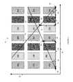
- FIGS. 4A-4Cillustrate example mesh designs of conductive lines 50 and 52 overlaid on an example display portion, similar to portion 20 .
- conductive lines 50 and 52 in the examples of FIGS. 4A-4Cmay be FLM and may be part of a mesh pattern of a touch sensor.
- Conductive lines 50 in FIGS. 4A-4Care substantially parallel to each other, and each conductive line 50 forming an angle 54 relative to horizontal axis 28 . Additionally, conductive lines 50 are substantially evenly spaced from one another with adjacent conductive lines 50 having an equal separation distance.
- Conductive lines 52 in FIGS. 4A-4Care also substantially parallel to each other, forming an angle 56 relative to horizontal axis 28 . Conductive lines 52 are also substantially evenly spaced from one another with adjacent conductive lines 52 having an equal separation distance.
- conductive lines 50 a and 50 bhave a separation distance 66 along horizontal axis 28 that is substantially equal to three times HPP 26 (or nine times HSPP 38 ) and conductive lines 52 a and 52 b have a separation distance 68 along horizontal axis 28 that is substantially equal to 13/6 times HPP 26 (or 6.5 times HSPP 38 ).
- the mesh design of FIG. 4Amay be preferable for a display with an HPP of approximately 150 ⁇ m. In the example mesh design of FIG.
- conductive lines 50 c and 50 dhave a separation distance 70 along horizontal axis 28 that is substantially equal to six times HPP 26 (or 18 times HSPP 38 ) and conductive lines 52 c and 52 d have a separation distance 72 along horizontal axis 28 that is substantially equal to 13/3 times HPP 26 (or 13 times HSPP 38 ).
- the mesh design of FIG. 4Bmay be preferable for a display with an HPP that is substantially less than 150 ⁇ m. In the example mesh design of FIG.
- conductive lines 50 e and 50 fhave a separation distance 74 along horizontal axis 28 that is substantially equal to two times HPP 26 (or six times HSPP 38 ) and conductive lines 52 e and 52 f have a separation distance 76 along horizontal axis 28 that is substantially equal to the sum of HPP 26 , HSPP 38 , dead space width 36 , and 1 ⁇ 2 of sub-pixel width 42 .
- the mesh design of FIG. 4Cmay be preferable for a display with an HPP of approximately 250 ⁇ m.
- conductive lines 50 and 52are substantially straight lines.
- non-linear conductive line patternsmay be used to avoid long linear stretches of conductive metal with a repeat frequency, which may reduce the appearance of interference or moiré patterns.
- one or more segments of one or more conductive lines 50 and 52may be substantially sinusoidal.
- conductive lines 50 and 52may have a sinusoidal variation with a peak-to-peak amplitude between 0 and 30 ⁇ m.
- conductive lines 50may have a sinusoidal variation with a period approximately equal to the separation distance between conductive lines 52 as measured along conductive lines 50 .
- conductive lines 52may have a sinusoidal variation with a period approximately equal to the separation distance between conductive lines 50 as measured along conductive lines 52 .
- this disclosuredescribes and illustrates particular meshes that have particular conductive lines 50 and 52 with particular curves (e.g., substantially straight or substantially sinusoidal), this disclosure contemplates any suitable meshes that have any suitable conductive lines with any suitable curves.
- FIG. 5illustrates the example mesh design of FIG. 4A over a larger portion 80 of an example display.
- the displaymay be an LCD, LED display, an LED backlight LCD, an electrophoretic display, a plasma display, or other suitable display and may include an array of pixels that each include three sub-pixels, as described above with reference to FIG. 2 .
- conductive lines 50 and 52overlie portion 80 .
- Conductive lines 50 and 52may be FLM and make up part of a mesh pattern of a touch sensor.
- this disclosuredescribes and illustrates a touch sensor overlying a display
- this disclosurecontemplates suitable portions of a touch sensor (including suitable portions of conductive lines 50 and 52 ) being disposed on one or more layers on or within a display stack of the display, where appropriate.
- conductive lines 50have a slope that equals SPH/HPP for the display that they overlie and a counterclockwise angle with respect to a horizontal axis across the display that equals the arctangent of SPH/HPP.
- Conductive lines 52have a slope that equals VP/2 ⁇ HSPP for the display that they overlie and a clockwise angle with respect to the same horizontal axis that equals the arctangent of VP/2 ⁇ HSPP.
- Conductive lines 50are substantially parallel to each other and substantially evenly spaced from one another.
- Conductive lines 52are also substantially parallel to each other and substantially evenly spaced from one another.
- the separation distance between adjacent conductive lines 50 along the horizontal axisis substantially equal to three times HPP (or nine times HSPP) for the display that they overlie, and the separation distance between adjacent conductive lines 52 along the horizontal axis is substantially equal to 13/6 times HPP (or 6.5 times HSPP) for the display that they overlie.
- a computer-readable non-transitory storage medium or mediamay include one or more semiconductor-based or other integrated circuits (ICs) (such, as for example, a field-programmable gate array (FPGA) or an application-specific IC (ASIC)), hard disk drives (HDDs), hybrid hard drives (HHDs), optical discs, optical disc drives (ODDs), magneto-optical discs, magneto-optical drives, floppy diskettes, floppy disk drives (FDDs), magnetic tapes, solid-state drives (SSDs), RAM-drives, SECURE DIGITAL cards, SECURE DIGITAL drives, any other suitable computer-readable non-transitory storage medium or media, or any suitable combination of two or more of these, where appropriate.
- ICssemiconductor-based or other integrated circuits
- HDDshard disk drives
- HHDshybrid hard drives
- ODDsoptical disc drives
- magneto-optical discsmagneto-optical drives
- FDDsfloppy diskettes
- FDDsf
- an apparatus or system or a component of an apparatus or systembeing adapted to, arranged to, capable of, configured to, enabled to, operable to, or operative to perform a particular function encompasses that apparatus, system, component, whether or not it or that particular function is activated, turned on, or unlocked, as long as that apparatus, system, or component is so adapted, arranged, capable, configured, enabled, operable, or operative.
Landscapes
- Physics & Mathematics (AREA)
- Engineering & Computer Science (AREA)
- Nonlinear Science (AREA)
- General Physics & Mathematics (AREA)
- General Engineering & Computer Science (AREA)
- Theoretical Computer Science (AREA)
- Mathematical Physics (AREA)
- Chemical & Material Sciences (AREA)
- Crystallography & Structural Chemistry (AREA)
- Optics & Photonics (AREA)
- Human Computer Interaction (AREA)
- Position Input By Displaying (AREA)
Abstract
Description
In the example of
In particular embodiments,
Claims (20)
Priority Applications (4)
| Application Number | Priority Date | Filing Date | Title |
|---|---|---|---|
| US13/910,055US8736571B1 (en) | 2013-06-04 | 2013-06-04 | Mesh design for touch sensors |
| TW103119428ATWI613579B (en) | 2013-06-04 | 2014-06-04 | Mesh design for touch sensors |
| CN201410244862.9ACN104216559B (en) | 2013-06-04 | 2014-06-04 | Mesh design for touch sensor |
| DE102014210581.1ADE102014210581A1 (en) | 2013-06-04 | 2014-06-04 | NET DESIGN FOR TOUCH SENSORS |
Applications Claiming Priority (1)
| Application Number | Priority Date | Filing Date | Title |
|---|---|---|---|
| US13/910,055US8736571B1 (en) | 2013-06-04 | 2013-06-04 | Mesh design for touch sensors |
Publications (1)
| Publication Number | Publication Date |
|---|---|
| US8736571B1true US8736571B1 (en) | 2014-05-27 |
Family
ID=50736484
Family Applications (1)
| Application Number | Title | Priority Date | Filing Date |
|---|---|---|---|
| US13/910,055ActiveUS8736571B1 (en) | 2013-06-04 | 2013-06-04 | Mesh design for touch sensors |
Country Status (4)
| Country | Link |
|---|---|
| US (1) | US8736571B1 (en) |
| CN (1) | CN104216559B (en) |
| DE (1) | DE102014210581A1 (en) |
| TW (1) | TWI613579B (en) |
Cited By (11)
| Publication number | Priority date | Publication date | Assignee | Title |
|---|---|---|---|---|
| US8896573B1 (en)* | 2014-01-21 | 2014-11-25 | Atmel Corporation | Line spacing in mesh designs for touch sensors |
| US8943903B1 (en)* | 2014-04-08 | 2015-02-03 | Atmel Corporation | Line spacing in mesh designs for touch sensors |
| US8947390B1 (en) | 2014-02-14 | 2015-02-03 | Atmel Corporation | Line spacing in mesh designs for touch sensors |
| CN104571713A (en)* | 2015-01-28 | 2015-04-29 | 昆山龙腾光电有限公司 | Touch panel and touch equipment using same |
| US20150355751A1 (en)* | 2014-06-10 | 2015-12-10 | Japan Display Inc. | Sensor-equipped display device |
| CN105320377A (en)* | 2014-06-10 | 2016-02-10 | 株式会社日本显示器 | Sensor-equipped display device |
| US9285942B1 (en) | 2014-10-27 | 2016-03-15 | Atmel Corporation | Optical-band visibility for touch-sensor mesh designs |
| US9304617B2 (en) | 2013-09-19 | 2016-04-05 | Atmel Corporation | Mesh design for touch sensors |
| US9454252B2 (en) | 2014-02-14 | 2016-09-27 | Atmel Corporation | Touch-sensor mesh design for display with complex-shaped sub-pixels |
| US20170308194A1 (en)* | 2016-04-20 | 2017-10-26 | Atmel Corporation | Touch Sensor Mesh Designs |
| US20200050301A1 (en)* | 2017-04-17 | 2020-02-13 | Eric PROVOST | Coupled Input and Information System |
Families Citing this family (4)
| Publication number | Priority date | Publication date | Assignee | Title |
|---|---|---|---|---|
| CN104932739B (en)* | 2015-05-11 | 2018-03-16 | 业成光电(深圳)有限公司 | Contact panel |
| CN105094424B (en)* | 2015-07-07 | 2018-10-09 | 业成光电(深圳)有限公司 | Touch display panel structure and touch-control display panel |
| CN112968046B (en)* | 2021-02-09 | 2022-11-29 | 湖北长江新型显示产业创新中心有限公司 | Display panel and display device |
| CN113534999B (en)* | 2021-07-13 | 2022-11-04 | 浙江鑫柔科技有限公司 | Touch sensor and display device including the same |
Citations (29)
| Publication number | Priority date | Publication date | Assignee | Title |
|---|---|---|---|---|
| US20010035924A1 (en)* | 2000-04-26 | 2001-11-01 | Ichiro Fujieda | Liquid crystal display device having a front light unit |
| US20080309635A1 (en) | 2007-06-14 | 2008-12-18 | Epson Imaging Devices Corporation | Capacitive input device |
| US20090315854A1 (en) | 2008-06-18 | 2009-12-24 | Epson Imaging Devices Corporation | Capacitance type input device and display device with input function |
| US7663607B2 (en) | 2004-05-06 | 2010-02-16 | Apple Inc. | Multipoint touchscreen |
| US20100149117A1 (en)* | 2008-12-11 | 2010-06-17 | Au Optronics Corporation | Color filter touch sensing substrate and display panel and manufacturing methods of the same |
| US7864503B2 (en) | 2007-05-11 | 2011-01-04 | Sense Pad Tech Co., Ltd | Capacitive type touch panel |
| US7875814B2 (en) | 2005-07-21 | 2011-01-25 | Tpo Displays Corp. | Electromagnetic digitizer sensor array structure |
| US7920129B2 (en) | 2007-01-03 | 2011-04-05 | Apple Inc. | Double-sided touch-sensitive panel with shield and drive combined layer |
| US20110148781A1 (en)* | 2009-12-22 | 2011-06-23 | Au Optronics Corporation | Touch display panel |
| US8031094B2 (en) | 2009-09-11 | 2011-10-04 | Apple Inc. | Touch controller with improved analog front end |
| US8031174B2 (en) | 2007-01-03 | 2011-10-04 | Apple Inc. | Multi-touch surface stackup arrangement |
| US8040326B2 (en) | 2007-06-13 | 2011-10-18 | Apple Inc. | Integrated in-plane switching display and touch sensor |
| US8049732B2 (en) | 2007-01-03 | 2011-11-01 | Apple Inc. | Front-end signal compensation |
| US20110291966A1 (en)* | 2010-05-28 | 2011-12-01 | Panasonic Corporation | Touch screen device |
| US20120044165A1 (en)* | 2010-08-19 | 2012-02-23 | Won-Kyu Kwak | Touch screen panel |
| US8179381B2 (en) | 2008-02-28 | 2012-05-15 | 3M Innovative Properties Company | Touch screen sensor |
| US8217902B2 (en) | 2007-04-27 | 2012-07-10 | Tpk Touch Solutions Inc. | Conductor pattern structure of capacitive touch panel |
| US20120242592A1 (en) | 2011-03-21 | 2012-09-27 | Rothkopf Fletcher R | Electronic devices with flexible displays |
| WO2012129247A2 (en) | 2011-03-21 | 2012-09-27 | Apple Inc. | Electronic devices with flexible displays |
| US20120243719A1 (en) | 2011-03-21 | 2012-09-27 | Franklin Jeremy C | Display-Based Speaker Structures for Electronic Devices |
| US20120243151A1 (en) | 2011-03-21 | 2012-09-27 | Stephen Brian Lynch | Electronic Devices With Convex Displays |
| US20120242588A1 (en) | 2011-03-21 | 2012-09-27 | Myers Scott A | Electronic devices with concave displays |
| US20120242606A1 (en)* | 2011-03-23 | 2012-09-27 | Synaptics Incorporated | Trace design for reduced visibility in touch screen devices |
| US20130076612A1 (en) | 2011-09-26 | 2013-03-28 | Apple Inc. | Electronic device with wrap around display |
| US20130100054A1 (en)* | 2009-10-29 | 2013-04-25 | Harald Philipp | Dual-Substrate-Sensor Stack With Electrodes Opposing a Display |
| US20130155000A1 (en)* | 2011-12-20 | 2013-06-20 | Matthew Trend | Touch sensor with reduced anti-touch effects |
| US20130294037A1 (en)* | 2011-01-18 | 2013-11-07 | Fujifilm Corporation | Conductive film and display apparatus provided with same |
| US8591279B1 (en)* | 2012-10-19 | 2013-11-26 | Eastman Kodak Company | Making display apparatus with pixel-aligned ground mesh |
| US20130342472A1 (en)* | 2012-06-26 | 2013-12-26 | David Brent GUARD | Pixel Occlusion Mitigation |
Family Cites Families (2)
| Publication number | Priority date | Publication date | Assignee | Title |
|---|---|---|---|---|
| US20090273577A1 (en)* | 2008-04-30 | 2009-11-05 | Apple Inc. | Moire-Free Touch Screen with Tilted or Curved ITO Pattern |
| CN101887324B (en)* | 2010-06-28 | 2012-10-03 | 友达光电股份有限公司 | Sensing-type display device |
- 2013
- 2013-06-04USUS13/910,055patent/US8736571B1/enactiveActive
- 2014
- 2014-06-04DEDE102014210581.1Apatent/DE102014210581A1/enactivePending
- 2014-06-04CNCN201410244862.9Apatent/CN104216559B/enactiveActive
- 2014-06-04TWTW103119428Apatent/TWI613579B/enactive
Patent Citations (29)
| Publication number | Priority date | Publication date | Assignee | Title |
|---|---|---|---|---|
| US20010035924A1 (en)* | 2000-04-26 | 2001-11-01 | Ichiro Fujieda | Liquid crystal display device having a front light unit |
| US7663607B2 (en) | 2004-05-06 | 2010-02-16 | Apple Inc. | Multipoint touchscreen |
| US7875814B2 (en) | 2005-07-21 | 2011-01-25 | Tpo Displays Corp. | Electromagnetic digitizer sensor array structure |
| US8049732B2 (en) | 2007-01-03 | 2011-11-01 | Apple Inc. | Front-end signal compensation |
| US7920129B2 (en) | 2007-01-03 | 2011-04-05 | Apple Inc. | Double-sided touch-sensitive panel with shield and drive combined layer |
| US8031174B2 (en) | 2007-01-03 | 2011-10-04 | Apple Inc. | Multi-touch surface stackup arrangement |
| US8217902B2 (en) | 2007-04-27 | 2012-07-10 | Tpk Touch Solutions Inc. | Conductor pattern structure of capacitive touch panel |
| US7864503B2 (en) | 2007-05-11 | 2011-01-04 | Sense Pad Tech Co., Ltd | Capacitive type touch panel |
| US8040326B2 (en) | 2007-06-13 | 2011-10-18 | Apple Inc. | Integrated in-plane switching display and touch sensor |
| US20080309635A1 (en) | 2007-06-14 | 2008-12-18 | Epson Imaging Devices Corporation | Capacitive input device |
| US8179381B2 (en) | 2008-02-28 | 2012-05-15 | 3M Innovative Properties Company | Touch screen sensor |
| US20090315854A1 (en) | 2008-06-18 | 2009-12-24 | Epson Imaging Devices Corporation | Capacitance type input device and display device with input function |
| US20100149117A1 (en)* | 2008-12-11 | 2010-06-17 | Au Optronics Corporation | Color filter touch sensing substrate and display panel and manufacturing methods of the same |
| US8031094B2 (en) | 2009-09-11 | 2011-10-04 | Apple Inc. | Touch controller with improved analog front end |
| US20130100054A1 (en)* | 2009-10-29 | 2013-04-25 | Harald Philipp | Dual-Substrate-Sensor Stack With Electrodes Opposing a Display |
| US20110148781A1 (en)* | 2009-12-22 | 2011-06-23 | Au Optronics Corporation | Touch display panel |
| US20110291966A1 (en)* | 2010-05-28 | 2011-12-01 | Panasonic Corporation | Touch screen device |
| US20120044165A1 (en)* | 2010-08-19 | 2012-02-23 | Won-Kyu Kwak | Touch screen panel |
| US20130294037A1 (en)* | 2011-01-18 | 2013-11-07 | Fujifilm Corporation | Conductive film and display apparatus provided with same |
| WO2012129247A2 (en) | 2011-03-21 | 2012-09-27 | Apple Inc. | Electronic devices with flexible displays |
| US20120243719A1 (en) | 2011-03-21 | 2012-09-27 | Franklin Jeremy C | Display-Based Speaker Structures for Electronic Devices |
| US20120243151A1 (en) | 2011-03-21 | 2012-09-27 | Stephen Brian Lynch | Electronic Devices With Convex Displays |
| US20120242588A1 (en) | 2011-03-21 | 2012-09-27 | Myers Scott A | Electronic devices with concave displays |
| US20120242592A1 (en) | 2011-03-21 | 2012-09-27 | Rothkopf Fletcher R | Electronic devices with flexible displays |
| US20120242606A1 (en)* | 2011-03-23 | 2012-09-27 | Synaptics Incorporated | Trace design for reduced visibility in touch screen devices |
| US20130076612A1 (en) | 2011-09-26 | 2013-03-28 | Apple Inc. | Electronic device with wrap around display |
| US20130155000A1 (en)* | 2011-12-20 | 2013-06-20 | Matthew Trend | Touch sensor with reduced anti-touch effects |
| US20130342472A1 (en)* | 2012-06-26 | 2013-12-26 | David Brent GUARD | Pixel Occlusion Mitigation |
| US8591279B1 (en)* | 2012-10-19 | 2013-11-26 | Eastman Kodak Company | Making display apparatus with pixel-aligned ground mesh |
Non-Patent Citations (4)
| Title |
|---|
| U.S. Appl. No. 14/031,372 (Guard), filed Sep. 19, 2013. |
| U.S. Appl. No. 61/454,894, filed Mar. 21, 2011, Rothkopf. |
| U.S. Appl. No. 61/454,936, filed Mar. 21, 2011, Myers. |
| U.S. Appl. No. 61/454,950, filed Mar. 21, 2011, Lynch. |
Cited By (22)
| Publication number | Priority date | Publication date | Assignee | Title |
|---|---|---|---|---|
| US9304617B2 (en) | 2013-09-19 | 2016-04-05 | Atmel Corporation | Mesh design for touch sensors |
| US8896573B1 (en)* | 2014-01-21 | 2014-11-25 | Atmel Corporation | Line spacing in mesh designs for touch sensors |
| US8947390B1 (en) | 2014-02-14 | 2015-02-03 | Atmel Corporation | Line spacing in mesh designs for touch sensors |
| US8947391B1 (en) | 2014-02-14 | 2015-02-03 | Atmel Corporation | Line spacing in mesh designs for touch sensors |
| US9454252B2 (en) | 2014-02-14 | 2016-09-27 | Atmel Corporation | Touch-sensor mesh design for display with complex-shaped sub-pixels |
| US9280246B2 (en)* | 2014-04-08 | 2016-03-08 | Atmel Corporation | Line spacing in mesh designs for touch sensors |
| US8943903B1 (en)* | 2014-04-08 | 2015-02-03 | Atmel Corporation | Line spacing in mesh designs for touch sensors |
| CN109002235B (en)* | 2014-06-10 | 2021-07-27 | 株式会社日本显示器 | sensor device |
| CN105320377A (en)* | 2014-06-10 | 2016-02-10 | 株式会社日本显示器 | Sensor-equipped display device |
| CN105278733A (en)* | 2014-06-10 | 2016-01-27 | 株式会社日本显示器 | Display unit with sensor |
| JP2015232817A (en)* | 2014-06-10 | 2015-12-24 | 株式会社ジャパンディスプレイ | Display device with sensor |
| US20150355751A1 (en)* | 2014-06-10 | 2015-12-10 | Japan Display Inc. | Sensor-equipped display device |
| US20180210581A1 (en)* | 2014-06-10 | 2018-07-26 | Japan Display Inc. | Sensor-equipped display device |
| US10156950B2 (en)* | 2014-06-10 | 2018-12-18 | Japan Display Inc. | Sensor-equipped display device |
| US9791984B2 (en)* | 2014-06-10 | 2017-10-17 | Japan Display Inc. | Sensor-equipped display device |
| CN109002235A (en)* | 2014-06-10 | 2018-12-14 | 株式会社日本显示器 | sensor device |
| US9952735B2 (en)* | 2014-06-10 | 2018-04-24 | Japan Display Inc. | Sensor-equipped display device |
| US9285942B1 (en) | 2014-10-27 | 2016-03-15 | Atmel Corporation | Optical-band visibility for touch-sensor mesh designs |
| CN104571713B (en)* | 2015-01-28 | 2017-06-13 | 昆山龙腾光电有限公司 | A kind of contact panel and use its touch control device |
| CN104571713A (en)* | 2015-01-28 | 2015-04-29 | 昆山龙腾光电有限公司 | Touch panel and touch equipment using same |
| US20170308194A1 (en)* | 2016-04-20 | 2017-10-26 | Atmel Corporation | Touch Sensor Mesh Designs |
| US20200050301A1 (en)* | 2017-04-17 | 2020-02-13 | Eric PROVOST | Coupled Input and Information System |
Also Published As
| Publication number | Publication date |
|---|---|
| TW201502940A (en) | 2015-01-16 |
| CN104216559A (en) | 2014-12-17 |
| DE102014210581A1 (en) | 2014-12-04 |
| TWI613579B (en) | 2018-02-01 |
| CN104216559B (en) | 2018-10-26 |
Similar Documents
| Publication | Publication Date | Title |
|---|---|---|
| US8736571B1 (en) | Mesh design for touch sensors | |
| US10659044B2 (en) | On-display-sensor stack | |
| US9154127B2 (en) | Touch sensor with conductive lines having portions with different widths | |
| US8917261B2 (en) | Pixel occlusion mitigation | |
| US20130180841A1 (en) | Sensor Stack with Opposing Electrodes | |
| US20130181910A1 (en) | Dual-Substrate-Sensor Stack | |
| US10044353B2 (en) | Substantially edgeless touch sensor | |
| US20150097801A1 (en) | Touch-sensor electrode details | |
| US9086770B2 (en) | Touch sensor with high-density macro-feature design | |
| US9152285B2 (en) | Position detection of an object within proximity of a touch sensor | |
| US9916047B2 (en) | Pattern of electrodes for a touch sensor | |
| US8896573B1 (en) | Line spacing in mesh designs for touch sensors | |
| US9760207B2 (en) | Single-layer touch sensor | |
| US10394402B2 (en) | Touch sensor with edge-balanced macro-feature design | |
| US9791992B2 (en) | Oncell single-layer touch sensor | |
| US10488976B2 (en) | Touch sensor mesh designs | |
| US9304617B2 (en) | Mesh design for touch sensors | |
| US20180143722A1 (en) | Integrated Pixel Display and Touch Sensor | |
| US20180032182A1 (en) | Variable-Pitch Tracking For Touch Sensors | |
| US9354734B2 (en) | Common-mode hover detection |
Legal Events
| Date | Code | Title | Description |
|---|---|---|---|
| AS | Assignment | Owner name:CONDUCTIVE INKJET TECHOLOGY LIMITED, UNITED KINGDO Free format text:ASSIGNMENT OF ASSIGNORS INTEREST;ASSIGNOR:BENTLEY, PHILIP GARETH;REEL/FRAME:030577/0902 Effective date:20130530 | |
| AS | Assignment | Owner name:ATMEL CORPORATION, CALIFORNIA Free format text:ASSIGNMENT OF ASSIGNORS INTEREST;ASSIGNOR:CONDUCTIVE INKJET TECHNOLOGY LIMITED;REEL/FRAME:030590/0829 Effective date:20130530 Owner name:ATMEL TECHNOLOGIES U.K. LIMITED, UNITED KINGDOM Free format text:ASSIGNMENT OF ASSIGNORS INTEREST;ASSIGNORS:GUARD, DAVID BRENT;EMM, STEVEN P.;REEL/FRAME:030585/0651 Effective date:20130611 | |
| AS | Assignment | Owner name:CONDUCTIVE INKJET TECHNOLOGY LIMITED, UNITED KINGD Free format text:CORRECTIVE ASSIGNMENT TO CORRECT THE ASSIGNEE'S NAME TO CONDUCTIVE INKJET TECHNOLOGY LIMITED PREVIOUSLY RECORDED ON REEL 030577 FRAME 0902. ASSIGNOR(S) HEREBY CONFIRMS THE ASSIGNEE'S NAME IS CONDUCTIVE INKJET TECHNOLOGY LIMITED;ASSIGNOR:BENTLEY, PHILIP GARETH;REEL/FRAME:030628/0841 Effective date:20130530 | |
| AS | Assignment | Owner name:ATMEL CORPORATION, CALIFORNIA Free format text:ASSIGNMENT OF ASSIGNORS INTEREST;ASSIGNOR:ATMEL TECHNOLOGIES U.K. LIMITED;REEL/FRAME:030807/0675 Effective date:20130703 | |
| AS | Assignment | Owner name:MORGAN STANLEY SENIOR FUNDING, INC. AS ADMINISTRATIVE AGENT, NEW YORK Free format text:PATENT SECURITY AGREEMENT;ASSIGNOR:ATMEL CORPORATION;REEL/FRAME:031912/0173 Effective date:20131206 Owner name:MORGAN STANLEY SENIOR FUNDING, INC. AS ADMINISTRAT Free format text:PATENT SECURITY AGREEMENT;ASSIGNOR:ATMEL CORPORATION;REEL/FRAME:031912/0173 Effective date:20131206 | |
| STCF | Information on status: patent grant | Free format text:PATENTED CASE | |
| AS | Assignment | Owner name:ATMEL CORPORATION, CALIFORNIA Free format text:TERMINATION AND RELEASE OF SECURITY INTEREST IN PATENT COLLATERAL;ASSIGNOR:MORGAN STANLEY SENIOR FUNDING, INC.;REEL/FRAME:038376/0001 Effective date:20160404 | |
| AS | Assignment | Owner name:JPMORGAN CHASE BANK, N.A., AS ADMINISTRATIVE AGENT, ILLINOIS Free format text:SECURITY INTEREST;ASSIGNOR:ATMEL CORPORATION;REEL/FRAME:041715/0747 Effective date:20170208 Owner name:JPMORGAN CHASE BANK, N.A., AS ADMINISTRATIVE AGENT Free format text:SECURITY INTEREST;ASSIGNOR:ATMEL CORPORATION;REEL/FRAME:041715/0747 Effective date:20170208 | |
| MAFP | Maintenance fee payment | Free format text:PAYMENT OF MAINTENANCE FEE, 4TH YEAR, LARGE ENTITY (ORIGINAL EVENT CODE: M1551) Year of fee payment:4 | |
| AS | Assignment | Owner name:JPMORGAN CHASE BANK, N.A., AS ADMINISTRATIVE AGENT, ILLINOIS Free format text:SECURITY INTEREST;ASSIGNORS:MICROCHIP TECHNOLOGY INCORPORATED;SILICON STORAGE TECHNOLOGY, INC.;ATMEL CORPORATION;AND OTHERS;REEL/FRAME:046426/0001 Effective date:20180529 Owner name:JPMORGAN CHASE BANK, N.A., AS ADMINISTRATIVE AGENT Free format text:SECURITY INTEREST;ASSIGNORS:MICROCHIP TECHNOLOGY INCORPORATED;SILICON STORAGE TECHNOLOGY, INC.;ATMEL CORPORATION;AND OTHERS;REEL/FRAME:046426/0001 Effective date:20180529 | |
| AS | Assignment | Owner name:WELLS FARGO BANK, NATIONAL ASSOCIATION, AS NOTES COLLATERAL AGENT, CALIFORNIA Free format text:SECURITY INTEREST;ASSIGNORS:MICROCHIP TECHNOLOGY INCORPORATED;SILICON STORAGE TECHNOLOGY, INC.;ATMEL CORPORATION;AND OTHERS;REEL/FRAME:047103/0206 Effective date:20180914 Owner name:WELLS FARGO BANK, NATIONAL ASSOCIATION, AS NOTES C Free format text:SECURITY INTEREST;ASSIGNORS:MICROCHIP TECHNOLOGY INCORPORATED;SILICON STORAGE TECHNOLOGY, INC.;ATMEL CORPORATION;AND OTHERS;REEL/FRAME:047103/0206 Effective date:20180914 | |
| AS | Assignment | Owner name:BOE TECHNOLOGY GROUP CO., LTD., CHINA Free format text:ASSIGNMENT OF ASSIGNORS INTEREST;ASSIGNOR:ATMEL CORPORATION;REEL/FRAME:050950/0594 Effective date:20191014 | |
| AS | Assignment | Owner name:ATMEL CORPORATION, ARIZONA Free format text:RELEASE BY SECURED PARTY;ASSIGNOR:JPMORGAN CHASE BANK, N.A., AS ADMINISTRATIVE AGENT;REEL/FRAME:050987/0430 Effective date:20191107 Owner name:MICROCHIP TECHNOLOGY INCORPORATED, ARIZONA Free format text:RELEASE BY SECURED PARTY;ASSIGNOR:WELLS FARGO BANK, NATIONAL ASSOCIATION, AS NOTES COLLATERAL AGENT;REEL/FRAME:050986/0798 Effective date:20191107 Owner name:ATMEL CORPORATION, ARIZONA Free format text:RELEASE BY SECURED PARTY;ASSIGNOR:WELLS FARGO BANK, NATIONAL ASSOCIATION, AS NOTES COLLATERAL AGENT;REEL/FRAME:050986/0798 Effective date:20191107 Owner name:MICROCHIP TECHNOLOGY INCORPORATED, ARIZONA Free format text:RELEASE BY SECURED PARTY;ASSIGNOR:JPMORGAN CHASE BANK, N.A., AS ADMINISTRATIVE AGENT;REEL/FRAME:050987/0430 Effective date:20191107 | |
| MAFP | Maintenance fee payment | Free format text:PAYMENT OF MAINTENANCE FEE, 8TH YEAR, LARGE ENTITY (ORIGINAL EVENT CODE: M1552); ENTITY STATUS OF PATENT OWNER: LARGE ENTITY Year of fee payment:8 | |
| AS | Assignment | Owner name:MICROSEMI STORAGE SOLUTIONS, INC., ARIZONA Free format text:RELEASE BY SECURED PARTY;ASSIGNOR:JPMORGAN CHASE BANK, N.A., AS ADMINISTRATIVE AGENT;REEL/FRAME:059333/0222 Effective date:20220218 Owner name:MICROSEMI CORPORATION, ARIZONA Free format text:RELEASE BY SECURED PARTY;ASSIGNOR:JPMORGAN CHASE BANK, N.A., AS ADMINISTRATIVE AGENT;REEL/FRAME:059333/0222 Effective date:20220218 Owner name:ATMEL CORPORATION, ARIZONA Free format text:RELEASE BY SECURED PARTY;ASSIGNOR:JPMORGAN CHASE BANK, N.A., AS ADMINISTRATIVE AGENT;REEL/FRAME:059333/0222 Effective date:20220218 Owner name:SILICON STORAGE TECHNOLOGY, INC., ARIZONA Free format text:RELEASE BY SECURED PARTY;ASSIGNOR:JPMORGAN CHASE BANK, N.A., AS ADMINISTRATIVE AGENT;REEL/FRAME:059333/0222 Effective date:20220218 Owner name:MICROCHIP TECHNOLOGY INCORPORATED, ARIZONA Free format text:RELEASE BY SECURED PARTY;ASSIGNOR:JPMORGAN CHASE BANK, N.A., AS ADMINISTRATIVE AGENT;REEL/FRAME:059333/0222 Effective date:20220218 | |
| AS | Assignment | Owner name:ATMEL CORPORATION, ARIZONA Free format text:RELEASE BY SECURED PARTY;ASSIGNOR:JPMORGAN CHASE BANK, N.A., AS ADMINISTRATIVE AGENT;REEL/FRAME:059262/0105 Effective date:20220218 | |
| AS | Assignment | Owner name:MICROSEMI STORAGE SOLUTIONS, INC., ARIZONA Free format text:RELEASE BY SECURED PARTY;ASSIGNOR:WELLS FARGO BANK, NATIONAL ASSOCIATION, AS NOTES COLLATERAL AGENT;REEL/FRAME:059358/0001 Effective date:20220228 Owner name:MICROSEMI CORPORATION, ARIZONA Free format text:RELEASE BY SECURED PARTY;ASSIGNOR:WELLS FARGO BANK, NATIONAL ASSOCIATION, AS NOTES COLLATERAL AGENT;REEL/FRAME:059358/0001 Effective date:20220228 Owner name:ATMEL CORPORATION, ARIZONA Free format text:RELEASE BY SECURED PARTY;ASSIGNOR:WELLS FARGO BANK, NATIONAL ASSOCIATION, AS NOTES COLLATERAL AGENT;REEL/FRAME:059358/0001 Effective date:20220228 Owner name:SILICON STORAGE TECHNOLOGY, INC., ARIZONA Free format text:RELEASE BY SECURED PARTY;ASSIGNOR:WELLS FARGO BANK, NATIONAL ASSOCIATION, AS NOTES COLLATERAL AGENT;REEL/FRAME:059358/0001 Effective date:20220228 Owner name:MICROCHIP TECHNOLOGY INCORPORATED, ARIZONA Free format text:RELEASE BY SECURED PARTY;ASSIGNOR:WELLS FARGO BANK, NATIONAL ASSOCIATION, AS NOTES COLLATERAL AGENT;REEL/FRAME:059358/0001 Effective date:20220228 |