US8736061B2 - Integrated circuits having a continuous active area and methods for fabricating same - Google Patents
Integrated circuits having a continuous active area and methods for fabricating sameDownload PDFInfo
- Publication number
- US8736061B2 US8736061B2US13/490,840US201213490840AUS8736061B2US 8736061 B2US8736061 B2US 8736061B2US 201213490840 AUS201213490840 AUS 201213490840AUS 8736061 B2US8736061 B2US 8736061B2
- Authority
- US
- United States
- Prior art keywords
- boundary
- integrated circuit
- interconnect
- standard cell
- gate
- Prior art date
- Legal status (The legal status is an assumption and is not a legal conclusion. Google has not performed a legal analysis and makes no representation as to the accuracy of the status listed.)
- Active
Links
Images


Classifications
- H—ELECTRICITY
- H10—SEMICONDUCTOR DEVICES; ELECTRIC SOLID-STATE DEVICES NOT OTHERWISE PROVIDED FOR
- H10D—INORGANIC ELECTRIC SEMICONDUCTOR DEVICES
- H10D89/00—Aspects of integrated devices not covered by groups H10D84/00 - H10D88/00
- H10D89/10—Integrated device layouts
- H—ELECTRICITY
- H01—ELECTRIC ELEMENTS
- H01L—SEMICONDUCTOR DEVICES NOT COVERED BY CLASS H10
- H01L23/00—Details of semiconductor or other solid state devices
- H01L23/52—Arrangements for conducting electric current within the device in operation from one component to another, i.e. interconnections, e.g. wires, lead frames
- H01L23/522—Arrangements for conducting electric current within the device in operation from one component to another, i.e. interconnections, e.g. wires, lead frames including external interconnections consisting of a multilayer structure of conductive and insulating layers inseparably formed on the semiconductor body
- H01L23/528—Layout of the interconnection structure
- H01L23/5286—Arrangements of power or ground buses
- H—ELECTRICITY
- H01—ELECTRIC ELEMENTS
- H01L—SEMICONDUCTOR DEVICES NOT COVERED BY CLASS H10
- H01L2924/00—Indexing scheme for arrangements or methods for connecting or disconnecting semiconductor or solid-state bodies as covered by H01L24/00
- H01L2924/0001—Technical content checked by a classifier
- H01L2924/0002—Not covered by any one of groups H01L24/00, H01L24/00 and H01L2224/00
- H—ELECTRICITY
- H10—SEMICONDUCTOR DEVICES; ELECTRIC SOLID-STATE DEVICES NOT OTHERWISE PROVIDED FOR
- H10D—INORGANIC ELECTRIC SEMICONDUCTOR DEVICES
- H10D84/00—Integrated devices formed in or on semiconductor substrates that comprise only semiconducting layers, e.g. on Si wafers or on GaAs-on-Si wafers
- H10D84/90—Masterslice integrated circuits
- H10D84/903—Masterslice integrated circuits comprising field effect technology
- H10D84/907—CMOS gate arrays
- H10D84/909—Microarchitecture
- H10D84/959—Connectability characteristics, i.e. diffusion and polysilicon geometries
Definitions
- the present disclosuregenerally relates to integrated circuits and methods for fabricating integrated circuits, and more particularly relates to integrated circuits having continuous active areas and methods for fabricating integrated circuits with continuous active regions.
- Standard cellsinclude active areas on which many gates are formed.
- the last gate formed on the active area(the gate formed nearest the end of the active area formed on the standard cell) exhibits problems.
- the transistor represented by the last gatehas performance problems including contact problems, yield problems, and variability problems. These problems arise from the inability to achieve a well-controlled, desirable structure at the end of the active area. For example, under current processing, gates formed at ends of active areas are troubled by undesirable epitaxial growth, facets, undercutting caused by wet etches, and undesirable material left in the topography.
- each standard cellcan be provided with an active area that extends from cell boundary to cell boundary.
- adjacent cellshave aligned active areas and form a continuous active area. As a result, last gates are minimized or eliminated.
- NMOS gatesIn order to utilize a continuous active area, gates on each side of the interface between standard cells must be isolated. Specifically, NMOS gates must be tied to ground and the PMOS gates must be tied to the power rail. Yet conventional tying methods, such as vias, result in use of a significant amount of IC area, leading to the design problems associated with the dummy gate methods noted above.
- an integrated circuitincludes a standard cell having a first boundary, a second boundary opposite the first boundary, a third boundary interconnecting the first and second boundaries, and a fourth boundary opposite the third boundary and interconnecting the first and second boundaries.
- the standard cellfurther includes parallel active areas extending from the first boundary to the second boundary.
- the standard cellhas parallel gate strips extending from the third boundary to the fourth boundary and over the active areas.
- a cut maskoverlies the gate strips.
- An interconnectis positioned overlying the cut mask and forms an electrical connection with a selected gate strip.
- an integrated circuitin another embodiment, includes an array of standard cells.
- Each standard cellincludes a first boundary, a second boundary opposite the first boundary, a third boundary interconnecting the first and second boundaries, and a fourth boundary opposite the third boundary and interconnecting the first and second boundaries.
- each standard cellhas an active area extending from the first boundary to the second boundary.
- each standard cellis provided with a gate strip extending from the third boundary to the fourth boundary and over the active area.
- a cut mask overlying terminal portions of the gate stripis provided.
- the integrated circuitincludes interconnects positioned along interfaces formed between the third boundaries and fourth boundaries of adjacent cells and overlying the respective cut masks. The interconnects form electrical connections with selected gate strips.
- a method for fabricating an integrated circuitincludes providing a plurality of standard cells. Each standard cell has a first boundary, a second boundary parallel to the first boundary, a third boundary interconnecting the first boundary and the second boundary, and a fourth boundary parallel to the third boundary.
- parallel active areasextending across each standard cell from the first boundary to the second boundary are formed.
- the methodalso forms parallel gate strips extending across each standard cell from the third boundary to the fourth boundary and over the active areas.
- a cut maskis deposited on each standard cell overlying the gate strips. Openings are formed in selected cut masks.
- a first interconnect portionis deposited across each standard cell from the first boundary to the second boundary and overlying the third boundary. Further, a second rail portion is deposited across each standard cell from the first boundary to the second boundary and overlying the fourth boundary.
- Selected interconnect portionsinclude extensions aligned with the openings to provide electrical connection between the selected interconnect portions and selected gate strips.
- FIG. 1illustrates a layout of a standard cell array, wherein the standard cells are shown with active areas and gate strips in accordance with various embodiments herein;
- FIG. 2illustrates a layout of the standard cell array of FIG. 1 , focusing on the interfaces between the cells, and includes a cut mask in accordance with various embodiments herein
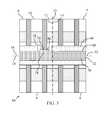
- FIG. 3illustrates the layout of FIG. 2 further including an interconnect to illustrate the electrical connection between the interconnect and the selected gate strip in accordance with various embodiments herein.
- continuous active areascan be utilized in integrated circuits to avoid or minimize the presence of last gates (i.e., gates otherwise bounded by insulating material at the end of an active area).
- the integrated circuits hereinisolate gates formed adjacent interfaces between adjacent standard cells by tying them to ground or power rails. Further, the integrated circuits herein avoid the use of vias or wires that consume IC space to connect the gates to the ground or power rails. Instead, it is envisioned herein that the interconnects forming the ground or power rails be selectively deposited directly onto interface-adjacent gates, thereby avoiding the use of additional IC space.
- FIGS. 1-3illustrate sequentially the layers forming such integrated circuits in accordance with various embodiments herein.
- steps in the design and composition of integrated circuitsare well known and so, in the interest of brevity, many conventional steps will only be mentioned briefly herein or will be omitted entirely without providing the well known process details. Further, it is noted that standard cells may include a varying number of components and that single components shown in the illustrations may be representative of multiple components.
- each standard cell 10has a first boundary 12 , a second boundary 14 opposite and parallel to the first boundary 12 , a third boundary 16 interconnecting the first boundary 12 and the second boundary 14 , and a fourth boundary 18 opposite and parallel to the third boundary 16 .
- Standard cells 10 adjacent in the direction 20e.g., standard cells 6 and 7
- Standard cells 10 adjacent in the direction 30form interfaces 32 at the respective third boundaries 16 and fourth boundaries 18 .
- Parallel active areas 40are formed on the standard cells 10 and extend across each standard cell 10 from the first boundary 12 to the second boundary 14 . As a result, when placed adjacent to a standard cell 10 in the direction 20 , continuous active areas 42 are formed. In other words, the active areas 40 are not bounded within the standard cells 10 , but instead connect and continue across horizontally-arranged standard cells 10 .
- parallel gate strips 50are also formed on the standard cells 10 . The gate strips 50 extend across each standard cell 10 from the third boundary 16 to the fourth boundary 18 . Further, the gate strips 50 extend over the active areas to form transistors.
- a cut mask 60is deposited over the terminal gates or portions 62 (identified in FIG. 1 ) of the gates strips 50 adjacent the interface 32 at the third boundary 16 of standard cells 6 and 7 and the fourth boundary 18 of standard cells 8 and 9 .
- the cut mask 60is formed from an insulating material and extends over the respective third boundary 16 and fourth boundary 18 from the respective first boundary 12 to the respective second boundary 14 .
- the cut mask 60cuts the continuity of the gate strips 50 between cells 6 and 9 , and between cells 7 and 8 .
- an opening 64is selectively formed in cut masks 60 .
- FIG. 3shows the integrated circuit 66 formed after depositing an interconnect 70 such as a ground or power rail.
- interconnect 70such as a ground or power rail.
- selected interconnects 70are connected to a power supply (not shown) that is employed, at least in part, in driving devices on the integrated circuit 66 , such as by providing a power supply voltage or potential.
- the interconnect 70may be a VDD interconnect.
- Other selected interconnects 70are connected to VSS (not shown) and may be ground interconnects.
- each standard cell 10a portion such as half 72 of the interconnect 70 is assigned to each standard cell 10 at the respective third boundaries 16 and fourth boundaries 18 . Therefore, while not shown in the FIGS., it is understood that cut masks 60 and interconnects 70 are provided at each third boundary 16 and fourth boundary 18 .
- Each interconnect 70is deposited over a respective cut mask 60 and extends from the respective first boundary 12 to the respective second boundary 14 .
- selected interconnect portions 74are provided with extensions 76 aligned with the openings 64 to provide electrical connection between the selected interconnects 70 and selected gate strips 50 . As shown, the extensions 76 extend in the direction 30 (identified in FIG. 1 ) to form extended edges 78 distanced from the non-extended edges 80 .
- the cut masks 60define opening edges 82 and body edges 84 .
- the electrical connection between the interconnect 70 and the gate strip 50has a contact area 86 with a width (in the direction 20 of FIG. 1 ) equal to a width of the gate strip 50 and a length (in the direction 30 of FIG. 1 ) of about 30 nm to about 40 nm, such as about 36 nm, i.e., the interconnect 70 (including extension 76 ) overlaps the gate strip 50 through the opening 64 by about 36 nm.
- the extended edge 78 of the interconnect 70is distanced from the nearest active area 40 by about 20 nm to about 30 nm, such as by about 27 nm, and the non-extended edge 80 of the interconnect 70 is distanced from the nearest active area 40 by about 40 nm to about 50 nm, such as about 46 nm.
- the opening edge 82 of the cut mask 60is distanced from the nearest active area 40 by about 60 nm to about 70 nm, such as by about 63 nm and the body edge 84 of the cut mask 60 is distanced from the nearest active area 40 by about 15 nm to about 25 nm, such as about 18 nm.
- the terminal gates 62 in the gate strips 50are isolated by selective tying to an interconnect 70 that is connected to the appropriate ground or a power supply. Further, the gates 62 are isolated by direct connection to the interconnect 70 , without requiring the use of vias or wires that would take up IC space.
Landscapes
- Design And Manufacture Of Integrated Circuits (AREA)
Abstract
Description
Claims (20)
Priority Applications (1)
| Application Number | Priority Date | Filing Date | Title |
|---|---|---|---|
| US13/490,840US8736061B2 (en) | 2012-06-07 | 2012-06-07 | Integrated circuits having a continuous active area and methods for fabricating same |
Applications Claiming Priority (1)
| Application Number | Priority Date | Filing Date | Title |
|---|---|---|---|
| US13/490,840US8736061B2 (en) | 2012-06-07 | 2012-06-07 | Integrated circuits having a continuous active area and methods for fabricating same |
Publications (2)
| Publication Number | Publication Date |
|---|---|
| US20130328205A1 US20130328205A1 (en) | 2013-12-12 |
| US8736061B2true US8736061B2 (en) | 2014-05-27 |
Family
ID=49714630
Family Applications (1)
| Application Number | Title | Priority Date | Filing Date |
|---|---|---|---|
| US13/490,840ActiveUS8736061B2 (en) | 2012-06-07 | 2012-06-07 | Integrated circuits having a continuous active area and methods for fabricating same |
Country Status (1)
| Country | Link |
|---|---|
| US (1) | US8736061B2 (en) |
Cited By (2)
| Publication number | Priority date | Publication date | Assignee | Title |
|---|---|---|---|---|
| US9640659B2 (en) | 2015-02-24 | 2017-05-02 | Samsung Electronics Co., Ltd. | Methods of fabricating semiconductor devices including hard mask patterning |
| US20190195555A1 (en)* | 2017-12-21 | 2019-06-27 | Shell Oil Company | System and method for operating a liquefaction train |
Families Citing this family (1)
| Publication number | Priority date | Publication date | Assignee | Title |
|---|---|---|---|---|
| JP2013183119A (en)* | 2012-03-05 | 2013-09-12 | Elpida Memory Inc | Semiconductor device and design method therefor |
Citations (7)
| Publication number | Priority date | Publication date | Assignee | Title |
|---|---|---|---|---|
| US20070243680A1 (en)* | 2006-04-13 | 2007-10-18 | Eliyahou Harari | Methods of Making Flash Memory Cell Arrays Having Dual Control Gates Per Memory Cell Charge Storage Element |
| US20080210981A1 (en)* | 2004-12-03 | 2008-09-04 | International Business Machines Corporation | Integrated Circuit Having Gates and Active Regions Forming a Regular Grating |
| US7554152B1 (en)* | 2006-01-11 | 2009-06-30 | National Semiconductor Corporation | Versatile system for integrated sense transistor |
| US7638851B2 (en)* | 2007-05-31 | 2009-12-29 | Hynix Semiconductor Inc. | Semiconductor device in peripheral circuit region using a dummy gate |
| US20100019280A1 (en)* | 2006-03-09 | 2010-01-28 | Tela Innovations, Inc. | Cell of Semiconductor Device Having Gate Electrode Conductive Structures Formed from Rectangular Shaped Gate Electrode Layout Features Defined Along At Least Four Gate Electrode Tracks |
| US20100214833A1 (en)* | 2004-05-25 | 2010-08-26 | Renesas Technology Corp. | Semiconductor device |
| US8513105B2 (en)* | 2010-10-14 | 2013-08-20 | Texas Instruments Incorporated | Flexible integration of logic blocks with transistors of different threshold voltages |
- 2012
- 2012-06-07USUS13/490,840patent/US8736061B2/enactiveActive
Patent Citations (8)
| Publication number | Priority date | Publication date | Assignee | Title |
|---|---|---|---|---|
| US20100214833A1 (en)* | 2004-05-25 | 2010-08-26 | Renesas Technology Corp. | Semiconductor device |
| US20080210981A1 (en)* | 2004-12-03 | 2008-09-04 | International Business Machines Corporation | Integrated Circuit Having Gates and Active Regions Forming a Regular Grating |
| US7554152B1 (en)* | 2006-01-11 | 2009-06-30 | National Semiconductor Corporation | Versatile system for integrated sense transistor |
| US20100019280A1 (en)* | 2006-03-09 | 2010-01-28 | Tela Innovations, Inc. | Cell of Semiconductor Device Having Gate Electrode Conductive Structures Formed from Rectangular Shaped Gate Electrode Layout Features Defined Along At Least Four Gate Electrode Tracks |
| US20100032726A1 (en)* | 2006-03-09 | 2010-02-11 | Tela Innovations, Inc. | Semiconductor Device Portion Having Sub-193 Nanometers -Sized Gate Electrode Conductive Structures Formed from Linear Shaped Gate Electrode Layout Features Defined Along At Least Four Gate Electrode Tracks with Minimum End-to-End Spacing and Having Corresponding Non-Symmetric Diffusion Regions |
| US20070243680A1 (en)* | 2006-04-13 | 2007-10-18 | Eliyahou Harari | Methods of Making Flash Memory Cell Arrays Having Dual Control Gates Per Memory Cell Charge Storage Element |
| US7638851B2 (en)* | 2007-05-31 | 2009-12-29 | Hynix Semiconductor Inc. | Semiconductor device in peripheral circuit region using a dummy gate |
| US8513105B2 (en)* | 2010-10-14 | 2013-08-20 | Texas Instruments Incorporated | Flexible integration of logic blocks with transistors of different threshold voltages |
Cited By (3)
| Publication number | Priority date | Publication date | Assignee | Title |
|---|---|---|---|---|
| US9640659B2 (en) | 2015-02-24 | 2017-05-02 | Samsung Electronics Co., Ltd. | Methods of fabricating semiconductor devices including hard mask patterning |
| US20190195555A1 (en)* | 2017-12-21 | 2019-06-27 | Shell Oil Company | System and method for operating a liquefaction train |
| US10571189B2 (en)* | 2017-12-21 | 2020-02-25 | Shell Oil Company | System and method for operating a liquefaction train |
Also Published As
| Publication number | Publication date |
|---|---|
| US20130328205A1 (en) | 2013-12-12 |
Similar Documents
| Publication | Publication Date | Title |
|---|---|---|
| US12148702B2 (en) | Semiconductor device with transistor local interconnects | |
| KR102149801B1 (en) | Standard-cell layout structure with horn power and smart metal cut | |
| DE102013111020B4 (en) | Semiconductor device and manufacturing method thereof | |
| US10777640B2 (en) | Standard cell architecture for gate tie-off | |
| US8581348B2 (en) | Semiconductor device with transistor local interconnects | |
| DE102012107756B4 (en) | FinFET based ESD devices and process for their manufacture | |
| DE112016007504T5 (en) | Integrated circuit device with crenelated metal trace layout | |
| US9935100B2 (en) | Power rail inbound middle of line (MOL) routing | |
| US20150052494A1 (en) | Power rail layout for dense standard cell library | |
| DE102014207415A1 (en) | Densely packed standard cells for integrated circuit products and methods of making same | |
| US9035389B2 (en) | Layout schemes for cascade MOS transistors | |
| TW201017451A (en) | Semiconductor integrated circuit device and a method of manufacturing the same | |
| US9634026B1 (en) | Standard cell architecture for reduced leakage current and improved decoupling capacitance | |
| US8736061B2 (en) | Integrated circuits having a continuous active area and methods for fabricating same | |
| CN102754214A (en) | Systems and methods for a continuous-well decoupling capacitor | |
| US7911003B2 (en) | Semiconductor integrated circuit device | |
| US9406663B2 (en) | Semiconductor devices | |
| JPWO2013018589A1 (en) | Semiconductor integrated circuit device | |
| DE102025107641A1 (en) | SEMICONDUCTOR DEVICE | |
| CN120111962A (en) | Chip unit layout design structure and integrated circuit | |
| JPS60119745A (en) | Manufacture of semiconductor integrated circuit device |
Legal Events
| Date | Code | Title | Description |
|---|---|---|---|
| AS | Assignment | Owner name:GLOBALFOUNDRIES INC., CAYMAN ISLANDS Free format text:ASSIGNMENT OF ASSIGNORS INTEREST;ASSIGNORS:JOHNSON, FRANK;TARABBIA, MARK;NORTHROP, GREGORY A.;AND OTHERS;SIGNING DATES FROM 20120228 TO 20120530;REEL/FRAME:028335/0985 | |
| AS | Assignment | Owner name:STMIRCOELECTRONICS INC., TEXAS Free format text:ASSIGNMENT OF ASSIGNORS INTEREST;ASSIGNORS:MENUT, OLIVIER;NORTHROP, GREGORY A.;JOHNSON, FRANK;AND OTHERS;SIGNING DATES FROM 20120228 TO 20120926;REEL/FRAME:029282/0233 Owner name:GLOBALFOUNDRIES INC., CAYMAN ISLANDS Free format text:ASSIGNMENT OF ASSIGNORS INTEREST;ASSIGNORS:MENUT, OLIVIER;NORTHROP, GREGORY A.;JOHNSON, FRANK;AND OTHERS;SIGNING DATES FROM 20120228 TO 20120926;REEL/FRAME:029282/0233 Owner name:INTERNATIONAL BUSINESS MACHINES CORPORATION, NEW Y Free format text:ASSIGNMENT OF ASSIGNORS INTEREST;ASSIGNORS:MENUT, OLIVIER;NORTHROP, GREGORY A.;JOHNSON, FRANK;AND OTHERS;SIGNING DATES FROM 20120228 TO 20120926;REEL/FRAME:029282/0233 | |
| AS | Assignment | Owner name:GLOBALFOUNDRIES INC., CAYMAN ISLANDS Free format text:CORRECTIVE ASSIGNMENT TO CORRECT THE ASSIGNEE: STMIRCOELECTRONICS INC. PREVIOUSLY RECORDED ON REEL 029282 FRAME 0233. ASSIGNOR(S) HEREBY CONFIRMS THE ASSIGNEE: STMICROELECTRONICS, INC.;ASSIGNORS:MENUT, OLIVIER;NORTHROP, GREGORY A.;JOHNSON, FRANK;AND OTHERS;SIGNING DATES FROM 20120228 TO 20120926;REEL/FRAME:029495/0394 Owner name:INTERNATIONAL BUSINESS MACHINES CORPORATION, NEW Y Free format text:CORRECTIVE ASSIGNMENT TO CORRECT THE ASSIGNEE: STMIRCOELECTRONICS INC. PREVIOUSLY RECORDED ON REEL 029282 FRAME 0233. ASSIGNOR(S) HEREBY CONFIRMS THE ASSIGNEE: STMICROELECTRONICS, INC.;ASSIGNORS:MENUT, OLIVIER;NORTHROP, GREGORY A.;JOHNSON, FRANK;AND OTHERS;SIGNING DATES FROM 20120228 TO 20120926;REEL/FRAME:029495/0394 Owner name:STMICROELECTRONICS, INC., TEXAS Free format text:CORRECTIVE ASSIGNMENT TO CORRECT THE ASSIGNEE: STMIRCOELECTRONICS INC. PREVIOUSLY RECORDED ON REEL 029282 FRAME 0233. ASSIGNOR(S) HEREBY CONFIRMS THE ASSIGNEE: STMICROELECTRONICS, INC.;ASSIGNORS:MENUT, OLIVIER;NORTHROP, GREGORY A.;JOHNSON, FRANK;AND OTHERS;SIGNING DATES FROM 20120228 TO 20120926;REEL/FRAME:029495/0394 | |
| STCF | Information on status: patent grant | Free format text:PATENTED CASE | |
| AS | Assignment | Owner name:STMICROELECTRONICS, INC., TEXAS Free format text:ASSIGNMENT OF ASSIGNORS INTEREST;ASSIGNOR:GLOBALFOUNDRIES, INC.;REEL/FRAME:033303/0210 Effective date:20140624 Owner name:INTERNATIONAL BUSINESS MACHINES CORPORATION, NEW Y Free format text:ASSIGNMENT OF ASSIGNORS INTEREST;ASSIGNOR:GLOBALFOUNDRIES, INC.;REEL/FRAME:033303/0210 Effective date:20140624 Owner name:GLOBALFOUNDRIES, INC., CAYMAN ISLANDS Free format text:ASSIGNMENT OF ASSIGNORS INTEREST;ASSIGNOR:GLOBALFOUNDRIES, INC.;REEL/FRAME:033303/0210 Effective date:20140624 | |
| AS | Assignment | Owner name:STMICROELECTRONICS, INC., TEXAS Free format text:ASSIGNMENT OF ASSIGNORS INTEREST;ASSIGNOR:MENUT, OLIVIER;REEL/FRAME:034096/0264 Effective date:20140124 | |
| MAFP | Maintenance fee payment | Free format text:PAYMENT OF MAINTENANCE FEE, 4TH YEAR, LARGE ENTITY (ORIGINAL EVENT CODE: M1551) Year of fee payment:4 | |
| AS | Assignment | Owner name:WILMINGTON TRUST, NATIONAL ASSOCIATION, DELAWARE Free format text:SECURITY AGREEMENT;ASSIGNOR:GLOBALFOUNDRIES INC.;REEL/FRAME:049490/0001 Effective date:20181127 | |
| AS | Assignment | Owner name:GLOBALFOUNDRIES INC., CAYMAN ISLANDS Free format text:RELEASE BY SECURED PARTY;ASSIGNOR:WILMINGTON TRUST, NATIONAL ASSOCIATION;REEL/FRAME:054479/0842 Effective date:20200410 Owner name:TAIWAN SEMICONDUCTOR MANUFACTURING CO., LTD., TAIWAN Free format text:ASSIGNMENT OF ASSIGNORS INTEREST;ASSIGNOR:GLOBALFOUNDRIES INC.;REEL/FRAME:054482/0862 Effective date:20200515 | |
| AS | Assignment | Owner name:GLOBALFOUNDRIES INC., CAYMAN ISLANDS Free format text:RELEASE BY SECURED PARTY;ASSIGNOR:WILMINGTON TRUST, NATIONAL ASSOCIATION;REEL/FRAME:054636/0001 Effective date:20201117 | |
| MAFP | Maintenance fee payment | Free format text:PAYMENT OF MAINTENANCE FEE, 8TH YEAR, LARGE ENTITY (ORIGINAL EVENT CODE: M1552); ENTITY STATUS OF PATENT OWNER: LARGE ENTITY Year of fee payment:8 |