US8735920B2 - Light emitting diode package with optical element - Google Patents
Light emitting diode package with optical elementDownload PDFInfo
- Publication number
- US8735920B2 US8735920B2US11/496,922US49692206AUS8735920B2US 8735920 B2US8735920 B2US 8735920B2US 49692206 AUS49692206 AUS 49692206AUS 8735920 B2US8735920 B2US 8735920B2
- Authority
- US
- United States
- Prior art keywords
- lens
- meniscus
- inner material
- led
- substrate
- Prior art date
- Legal status (The legal status is an assumption and is not a legal conclusion. Google has not performed a legal analysis and makes no representation as to the accuracy of the status listed.)
- Active
Links
Images


Classifications
- H—ELECTRICITY
- H10—SEMICONDUCTOR DEVICES; ELECTRIC SOLID-STATE DEVICES NOT OTHERWISE PROVIDED FOR
- H10H—INORGANIC LIGHT-EMITTING SEMICONDUCTOR DEVICES HAVING POTENTIAL BARRIERS
- H10H20/00—Individual inorganic light-emitting semiconductor devices having potential barriers, e.g. light-emitting diodes [LED]
- H10H20/80—Constructional details
- H10H20/85—Packages
- H10H20/8506—Containers
- H—ELECTRICITY
- H01—ELECTRIC ELEMENTS
- H01L—SEMICONDUCTOR DEVICES NOT COVERED BY CLASS H10
- H01L2224/00—Indexing scheme for arrangements for connecting or disconnecting semiconductor or solid-state bodies and methods related thereto as covered by H01L24/00
- H01L2224/01—Means for bonding being attached to, or being formed on, the surface to be connected, e.g. chip-to-package, die-attach, "first-level" interconnects; Manufacturing methods related thereto
- H01L2224/42—Wire connectors; Manufacturing methods related thereto
- H01L2224/47—Structure, shape, material or disposition of the wire connectors after the connecting process
- H01L2224/48—Structure, shape, material or disposition of the wire connectors after the connecting process of an individual wire connector
- H01L2224/4805—Shape
- H01L2224/4809—Loop shape
- H01L2224/48091—Arched
- H—ELECTRICITY
- H10—SEMICONDUCTOR DEVICES; ELECTRIC SOLID-STATE DEVICES NOT OTHERWISE PROVIDED FOR
- H10H—INORGANIC LIGHT-EMITTING SEMICONDUCTOR DEVICES HAVING POTENTIAL BARRIERS
- H10H20/00—Individual inorganic light-emitting semiconductor devices having potential barriers, e.g. light-emitting diodes [LED]
- H10H20/01—Manufacture or treatment
- H10H20/036—Manufacture or treatment of packages
- H10H20/0362—Manufacture or treatment of packages of encapsulations
- H—ELECTRICITY
- H10—SEMICONDUCTOR DEVICES; ELECTRIC SOLID-STATE DEVICES NOT OTHERWISE PROVIDED FOR
- H10H—INORGANIC LIGHT-EMITTING SEMICONDUCTOR DEVICES HAVING POTENTIAL BARRIERS
- H10H20/00—Individual inorganic light-emitting semiconductor devices having potential barriers, e.g. light-emitting diodes [LED]
- H10H20/80—Constructional details
- H10H20/85—Packages
- H10H20/852—Encapsulations
- H10H20/854—Encapsulations characterised by their material, e.g. epoxy or silicone resins
- H—ELECTRICITY
- H10—SEMICONDUCTOR DEVICES; ELECTRIC SOLID-STATE DEVICES NOT OTHERWISE PROVIDED FOR
- H10H—INORGANIC LIGHT-EMITTING SEMICONDUCTOR DEVICES HAVING POTENTIAL BARRIERS
- H10H20/00—Individual inorganic light-emitting semiconductor devices having potential barriers, e.g. light-emitting diodes [LED]
- H10H20/80—Constructional details
- H10H20/85—Packages
- H10H20/855—Optical field-shaping means, e.g. lenses
Definitions
- This inventionrelates to semiconductor light emitting diodes (LEDs) and more particularly to LED packages with optical elements.
- LEDsLight emitting diodes
- LEDsare solid state devices that convert electric energy to light, and generally comprise one or more active layers of semiconductor material sandwiched between oppositely doped layers. When a bias is applied across the doped layers, holes and electrons are injected into the active layer where they recombine to generate light. Light is emitted from the active layer and from all surfaces of the LED. The useful light is generally emitted in the direction of the LED's top surface.
- LEDscannot generate white light from their active layers.
- One way to produce white light from conventional LEDsis to combine different colors from different LEDs. For example, the light from red, green and blue LEDs, or blue and yellow LEDs can be combined to produce white light.
- different colors of lightare often generated from different types of LEDs which can require complex fabrication to combine in one device. The resulting devices can also require complicated control electronics since the different diode types can require different control voltages. Long term wavelength and stability of these devices is also degraded by the different aging behavior of the different LEDs.
- Light from a single blue emitting LEDhas been converted to white light by surrounding the LED with a yellow phosphor, polymer or dye.
- a yellow phosphor, polymer or dyeSee Nichia Corp. white LED, Part No. NSPW300BS, NSPW312BS, etc., which comprise blue LEDs surrounded by a yellow phosphor powder; see also U.S. Pat. No. 5,959,316 to Lowery, entitled Multiple Encapsulation of Phosphor-LED Devices.
- the surrounding materialdownconverts the wavelength of some of the LED light, changing its color.
- a nitride based blue emitting LED chipcan be surrounded by a yellow phosphor. Some of the blue light will pass through the phosphor without being changed while the remaining light will be downconverted to yellow. The LED will emit both blue and yellow light, which combine to produce white light.
- Another example of LEDs using this approachincludes U.S. Pat. No. 5,813,753 to Vriens et al.
- LED packagestypically have some type of encapsulant surrounding the LED chip to enhance light extraction from the chip and protect the chip and related contacts structure (e.g. wire bonds) from exposure to physical damage or environmental conditions which could lead to corrosion or degradation.
- an optical elementsuch as a simple hemispherical lens is also desired to enhance light extraction from the package and possibly to provide some form of output light beam shaping (control over the angle-dependent emission properties of the lamp).
- the possible materialstypically include silicones and glasses.
- Silicone lensesare typically molded using injection molding processes, which can place limitations on the properties of the silicone that may be used. Glass lenses are typically formed using a melting process that can limit the possible geometries and add substantial piece part cost to the final lamp.
- Typical wire bonded LEDscannot be encapsulated in molten glass because of the high melting temperature of glass.
- Present surface-mount LED package technologytypically utilizes either a separate glass lens or a molded silicone lens.
- These lensesrepresent separate piece parts that must be affixed to the part during package assembly. The parts also represent additional cost due to the required lens fabrication, and may be difficult to attach.
- the lensescan also be made of materials (e.g. silicone) with a different coefficient of thermal expansion (CTE) compared to the surrounding package components. This can result in the cracking or delaminating of the LED chip or package elements, both of which can reduce light extraction from the LED package. This difference in CTE can also result in damage to the LED chip, and in particular the wire bond can be broken or pulled from the LED resulting in failure of the LED package.
- CTEcoefficient of thermal expansion
- LED packagecomprises a substrate with an LED chip mounted to the substrate and in electrical contact with said substrate.
- An inner materialcovering the LED chip and a lens covering the inner material and being harder than the inner material.
- An adhesiveis arranged between the substrate and the lens, the adhesive holding the lens to the substrate and compensating for different coefficients of thermal expansion (CTE) between the lens the remainder of the package.
- an LED package according to the present inventioncomprises a substrate and an LED chip mounted to the substrate and in electrical contact with the substrate.
- a lensis included having a substrate contacting surface. The lens is made of a material harder than said inner material and is mounted on the substrate, over said inner material at its mounting surface. The meniscus holding feature defines the edge of the lens mounting surface.
- an LED arraycomprises a plurality of LED chips mounted on a substrate, with the substrate arranged to apply an electrical signal to each of the LED chips.
- An inner materialcovers at least one of the LED chips, and a lens comprising a material harder than the inner material and covering each of the inner material.
- An adhesiveis arranged between the substrate and each of the lenses, with the adhesive holding the lens to the substrate and compensating for different coefficients of thermal expansion between the lens the remainder of the package.
- One embodiment of a method for forming an LED package according to the present inventioncomprises providing a substrate with a first meniscus ring on a surface of the substrate.
- An LED chipis mounted to the substrate, within the meniscus ring.
- An inner materialis deposited over the LED chip, and a lens material in liquid form is deposited over the inner material, with the lens material held in a hemispheric shape by the first meniscus feature.
- the lens materialis then cured making it harder than the inner material.
- FIG. 1is a sectional view of one embodiment of an LED package according to the present invention having a meniscus holding feature, inner material and outer lens;
- FIG. 2is a sectional view of another embodiment of an LED package according to the present invention comprising a different meniscus holding feature
- FIG. 3is a sectional view of another embodiment of an LED package according to the present invention comprising a transparent meniscus holding feature
- FIG. 4is a sectional view of another embodiment of an LED package according to the present invention with a different transparent meniscus holding feature
- FIG. 5is a sectional view of still another embodiment of an LED package according to the present invention with a transparent meniscus holding feature
- FIG. 6is a sectional view of another embodiment of an LED package according to the present invention having a separately formed piece part lens
- FIG. 7is a sectional view of another embodiment of an LED package according to the present invention having a separately formed piece part lens and multiple LED chips;
- FIG. 8is a sectional view of another embodiment of an LED package according to the present invention having a separately formed piece part lens
- FIG. 9is a sectional view of one embodiment of an LED array according to the present invention.
- FIG. 10is a sectional view of another embodiment of an LED package according to the present invention having an LED chip without wire bonds;
- FIG. 11is a flow diagram for one embodiment of a method according to the present invention.
- the present inventioncomprises a dispensed optical element or lens that may be fabricated directly on the LED lamp using common processing (e.g. dispensing) processes and equipment.
- the inventionis particularly applicable to fabricating LED packages without the need for additional piece part (i.e. separately formed) lenses, although aspects of this invention can also be used with packages utilizing piece part fabricated lenses.
- the dispensed lens embodiments according to the present inventionmay be fabricated using a variety of available silicone or epoxy materials, allowing application to surface mount LED packages or arrays.
- Surface features, herein referred to as meniscus forming features or meniscus rings,may be included on the LED package to allow a substantially hemispherical lens to be formed from a liquid lens material by allowing formation of a meniscus.
- the term “substantially hemispherical” and related termsare meant to convey a variety of curved surfaces, including but not limited to ones having essentially elliptical cross-section.
- the lenscan be cured or processed to provide a stable surface.
- the geometry of the resulting lensmay be controlled using the geometry of the meniscus forming features, the rheology of the dispensed material or materials, the processing steps (e.g. sequential dispense steps of different materials or followed by specific process steps such as curing, etc.), the curing or processing orientation (e.g. parts may be cured or processing in an inverted position in order to utilize gravitational effects).
- the geometrycan also be controlled by the application of surface energy modifying compounds to various surfaces either inside or outside the meniscus forming features (e.g., the use of a anti-wetting coating such as a fluorocarbon polymer having a surface energy well below the surface tension of the lens material) to reduce the chance of the lens material “breaking out” of the meniscus thereby allowing the build-up of higher lens features, and other factors which may effect the surface energy of the dispensed liquid prior to processing or curing.
- the adhesive materialsuch as an adhesive silicone may be used in conjunction with the lens to improve attachment strength of the lens and to compensate for CTE mismatches between the cured lens and other LED package materials.
- the dispensed lenscan provide a reproducible lens with a smooth finish without the need for procuring and handling additional lens piece parts.
- the encapsulants used for surface mount LED packagesare typically comprised of silicones
- the dispensed lensmay be fabricated from a similar silicone material which is compatible in terms of chemical nature, thermal expansion properties, adhesion, etc.
- a variety of hard silicone materialshave been developed that are well suited for a dispensing and curing to form a protective surface. In many cases these same materials are not well suited to forming piece part lenses by injection molding.
- the dispensed lens processprovides a convenient method for forming a large number of reproducible optical elements in an efficient and inexpensive manner.
- the present inventionutilizes materials of different polymetric hardness in different locations to form a reliable LED package with a hard encapsulant or lens protecting the LED chip and its electrical connections.
- One method for measuring hardness of polymetric materialsis by Shore durometers, with rigid materials registering a high durometer reading and soft gel-like materials registering a low durometer reading.
- Packages according to the present inventionhave one or more LEDs mounted to a package or substrate, with one package being a surface mount package having a ceramic substrate.
- Soft stable inner materials having low durometer readingse.g. less than 50 on Shore durometer 00 scale
- the soft materialis preferably in a substantially hemispheric shape over the LED.
- the soft materialcan enhance light extraction from the LED chip and protect the chip and wire bonds from exposure to physical damage or environmental conditions. During thermal cycles, the soft material also reduces failure by allowing the LED wire bonds to “flex” or even “cut” through the soft material during expansion or contraction, instead of being pulled from the LED or package bonding surfaces, or broken.
- a harder outer material with a higher durometer readingare provided over the soft material also in a substantially hemispheric shaped encapsulant or lens (“lens”).
- a silicone adhesivecan be provided between the harder hemispheric lens and the package substrate (and lens) with the adhesive also having a lower durometer reading than the lens, preferable with rubbery and/or elastic characteristics.
- the silicone adhesiveholds the lens to the package while at the same time compensating for CTE mismatches between the LED package and lens.
- the low durometer characteristics of the silicone adhesiveallow it to stretch or deform. This allows the lens to be held to the package without delaminating or cracking.
- LED packages according to the present inventioncan have one or more meniscus holding features that allow the different materials to be dispensed in liquid form on the package and held in the desired substantially hemispheric shape until cured.
- Meniscus forming featuresgenerally comprise a physical transition that is arranged so that a meniscus forms by surface tension between a liquid and the physical transition.
- the term “meniscus”refers to the convex surface of liquid which is formed by surface tension.
- the physical transitionscan be features such as edges, corners, ledges, trenches, rings, and any other physical transition that creates a meniscus when a liquid surface comes in contact with it.
- the meniscus holding featuresare primarily described below as rings, but it is understood that the meniscus holding features can have many different shapes such as square or oval with these influencing the overall shape of the liquid held by the feature.
- an inner meniscus ringcan be provided on the package substrate, around the LED chip, and the soft low durometer reading material can be dispensed in a liquid on the package substrate, over the LED chip.
- the meniscus formed between the inner ring and the dispensed materialforms the material in a substantially hemispheric shape over the LED.
- the materialcan then be cured to its soft, low durometer state.
- An outer meniscus holding ringcan be included on the package substrate, around the soft inner material.
- the material for the lens (encapsulant)can be dispensed in liquid form over the soft material.
- the outer meniscus holding featureholds the lens material in a substantially hemispheric shape over the softer material and is cured to its hardened state.
- an adhesive siliconecan be included to adhere the lens to the package and to compensate for mismatches in CTE.
- the inner soft material and lenscan also include light conversion materials such as phosphors, and also light scattering particles.
- first, second, etc.may be used herein to describe various elements, components, regions, layers and/or sections, these elements, components, regions, layers and/or sections should not be limited by these terms. These terms are only used to distinguish one element, component, region, layer or section from another region, layer or section. Thus, a first element, component, region, layer or section discussed below could be termed a second element, component, region, layer or section without departing from the teachings of the present invention.
- Embodiments of the inventionare described herein with reference to cross-sectional view illustrations that are schematic illustrations of idealized embodiments of the invention. As such, variations from the shapes of the illustrations as a result, for example, of manufacturing techniques and/or tolerances are expected. Embodiments of the invention should not be construed as limited to the particular shapes of the regions illustrated herein but are to include deviations in shapes that result, for example, from manufacturing. A region illustrated or described as square or rectangular will typically have rounded or curved features due to normal manufacturing tolerances. Thus, the regions illustrated in the figures are schematic in nature and their shapes are not intended to illustrate the precise shape of a region of a device and are not intended to limit the scope of the invention.
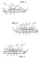
- FIG. 1shows one embodiment of LED package 10 according to the present invention that comprises a surface mount substrate 12 .
- a surface mount substrate 12can comprise a ceramic core 16 with conductive features 14 deposited on surfaces of the core 16 .
- the conductive featurescan comprise conductive traces made of a conductive material such as plated copper.
- the surface mount substrate 12is arranged to be mounted to a final fixture using solder reflow processes known in the art.
- the package 10also comprises an LED chip 18 mounted to the substrate 12 using known mounting methods. In other embodiments more than one LED chip can be included. The details of operation and fabrication of conventional LED chips are also generally known in the art and are only briefly discussed. Conventional LEDs can be fabricated by known methods, with a suitable method being fabrication by Metal Organic Chemical Vapor Deposition (MOCVD). In operation, an electrical signal can be applied across the LED's oppositely doped layer causing the LED's active region to emit light.
- MOCVDMetal Organic Chemical Vapor Deposition
- the LED chip 18is in electrical contact with the conductive features 14 such that a bias applied to the conductive features 14 is conducted to the LED chip 18 , causing it to emit light. It is understood that the LED chip 18 can be in electrical contact with the substrate using different arrangements depending on factors such as the LED chip geometry and layout of the conductive features 14 . In the embodiment shown, the LED chip is contacted by a wirebond 20 and through its contacting surface with the substrate. In other embodiments, more than one wire bond can be used or the LED chip can be contacted in different ways. It is further understood that in some embodiments, the LED chip is not in electrical contact with the substrate.
- An inner material 22is provided over the LED chip 18 and at least part of the wire bond 20 that is preferably soft (low durometer reading) and preferably formed in a substantially hemispheric shape over the LED chip 18 .
- the inner material 22can be dispensed in liquid form over the LED chip and then cured to its low durometer state.
- an inner meniscus ringcan be included around the LED chip 18 to hold the inner material 22 in its hemispheric shape.
- the inner materialcan be held in its hemispheric shape by surface tension between the top of the substrate 12 and the dispensed material.
- the inner materialcan comprise many different materials alone or in combination, with a suitable material being a soft silicone having a low durometer reading, commercially available from Nye Lubricants, Inc.
- the inner materialcan also comprise light conversion materials, such as phosphors.
- the LED chip 18emits light in the blue wavelength spectrum and the phosphor absorbs some of the blue light and re-emits yellow.
- the led package 10emits a white light combination of blue and yellow light.
- a full range of broad yellow spectral emissionis possible using conversion particles made of phosphors based on the (Gd,Y) 3 (Al,Ga) 5 O 12 :Ce system.
- the following lists other suitable phosphors used as conversion particles in an LED package 10although others can be used. Each exhibits excitation in the blue and/or UV emission spectrum, provides a desirable peak emission, has efficient light conversion, and has acceptable Stokes shift:
- the conversion materialscan have different concentrations in the inner material 22 depending on the conversion efficiency of the material.
- the conversion particlescan be uniformly dispersed in the inner material, or the particles can settle around the LED so that the particles are closer to the LED.
- the inner material 22can also contain materials to help scatter the light, such as scattering particles. Once the inner material 22 is dispensed in, it can be cured using known methods, such as heat or UV curing, to harden.
- the LED package 10further comprises an outer meniscus holding ring 24 that can be included on the substrate 12 , around the soft inner material 22 .
- the meniscus holding ring 24comprises the edge of disc 26 on the substrate surface.
- the disccan be made of many different materials, with a suitable material being etched plated copper.
- the material for the lens (encapsulant) 28is dispensed in liquid form over the inner material 22 .
- the outer meniscus holding featureholds the material for the lens 28 in a substantially hemispheric shape over the inner material 22 , and is cured to its hardened state having a high durometer reading.
- the lenscan be cured to a rigid material or can be cured to a rubbery/elastic material.
- Many different materialscan be used for the lens, with a suitable material being Sylgard® 184 commercially available from Dow Corning. In other embodiments a commercially available epoxy may be used.
- the CTE mismatch between the lens 28 and the substrate 12may not cause delamination or cracking.
- delamination or crackingmay be a greater concern.
- a layer of adhesive 30can be included to adhere the lens 28 to the substrate 12 and to compensate for CTE mismatches.
- the adhesive 30can cover all of the surface of the substrate 12 between the lens 28 and substrate 12 , or a portion of the surface.
- the adhesive 30can also be in other are areas, such as between the inner material 22 and the lens 28 .
- the adhesive 30can be applied using many different methods, such as known dispensing methods. Many different materials can be used for the adhesive, with a suitable material being an adhesive silicone such as GE 3221S commercially available from General Electric.
- the silicone adhesivepreferably has a durometer reading higher than the inner material 22 such that it has flexible properties but is rigid enough to firmly adhere the lens 28 to the substrate. During temperature cycles, the substrate 12 and lens 28 can expand and contract at different rates depending on the CTE of the materials.
- the silicone adhesiveis arranged to compensate for the CTE mismatches to prevent delamination and cracking.
- most of the wire bond 20is in the soft inner material, with a portion of it in the lens 28 .
- all of the wire bond 20is in the inner material.
- FIG. 2shows another embodiment of an LED package 40 according to the present invention comprising a substrate 42 with conductive elements 44 , LED chip 48 and wire bond 50 similar to those in the LED package 10 in FIG. 1 and described above.
- the package 10further comprises a meniscus ring 52 around the LED chip 48 , with the ring 52 having a generally U-shaped cross-section.
- the ring 52can be a lead frame or stamped part mounted to the substrate 42 using known mounting methods.
- the ring's inner portionbeing angled to form a cup 54 .
- the surface of the cupcan be reflective to reflect out sideways emitted light from the LED chip 48 .
- the cupis also arranged to hold inner material 56 that is similar to the inner material 22 in FIG. 1 .
- the materialis preferably a soft silicone that can have phosphor materials and scattering particles.
- the wire bond 50can be completely in the soft inner material as shown, and in other embodiments can be in other locations.
- the upper edge 55 of the cup 54can serve as a physical transition and meniscus holding feature.
- the inner material 56is dispensed into the cup 54 in liquid form, the meniscus formed at the upper edge 55 can hold the inner material with a curved upper surface 58 .
- the liquidcan be held this way until cured to its soft state.
- the soft materialallows for expansion and contraction of the inner material during thermal cycles with the wire bond 50 cutting through the material instead of the material breaking or pulling from its contact point.
- the meniscus ringalso comprises an outer portion 60 that serves as the physical transition and meniscus holding feature for the material that forms the lens 62 .
- the lens materialcan then be cured to form the lens 62 .
- the lens 62can be made of many different materials, with a suitable material being the material used for lens 28 in FIG. 1 .
- an adhesive 64can be included primarily between the meniscus ring 52 and the lens 62 . In other embodiments, although, it can also be included between the inner material 56 and the lens 62 .
- the adhesive 64can be made of many different materials, but is preferably made of the same material used for adhesive 30 in FIG. 1 .
- the package 40can also comprise a known electrostatic discharge (ESD) chip 66 to protect the LED chip 48 and the remainder of the package 40 from damage caused by electrostatic discharge.
- ESDelectrostatic discharge
- FIG. 3shows another embodiment of an LED package 70 according to the present invention having many elements similar to those in the LED package 40 in FIG. 2 .
- the same reference numbersare used with the understanding that the description of those referenced from FIG. 2 applies to the reference number herein.
- the LED package 70comprises a substrate 42 , LED chip 48 , wire bond 50 , inner material 56 , lens 62 , adhesive layer 64 and ESD chip 66 .
- the package 70also comprises a meniscus ring 72 around the LED chip 48 that can also be a lead frame or stamped part.
- the meniscus ring 72has a cross section different from the meniscus ring 52 in FIG. 2 .
- the inner surface of the meniscus ringis angled to form a cup 74 with a reflective surface and an upper edge 76 that serves as the meniscus holding feature for the inner material 56 .
- the outer edge 78 of the meniscus ring 72serves as the meniscus holding feature of the material that forms the lens 62 . This outer edge 78 forms a meniscus with the lens material and holds the material in substantially hemispheric shape until cured.
- FIG. 4shows another embodiment of an LED package 90 according to the present invention comprising a substrate 42 , LED chip 48 , wire bond 50 , inner material 56 , lens 62 , adhesive layer 64 and ESD chip 66 .
- the package 90also comprises a meniscus ring 92 that is not a lead frame or stamped part, but is instead made of a transparent material such as a molded hard silicone or glass. By being transparent, the meniscus ring 92 allows for more of the sideways emitted light from the LED chip 48 to pass through the meniscus ring 92 and emit light from the sides of the LED package 90 , instead of being reflected. This allows for improved sideways emission for the LED package 90 .
- the inner surface 94 of the meniscus ring 92can be vertical.
- the upper edge 96serves as the meniscus holding feature for the inner material 56 .
- the meniscus holding feature of the material that forms the lens 62is the outer edge 98 of the meniscus ring 92 .
- the outer edge 98forms the meniscus to hold the lens material in a substantially hemispheric shape until cured.
- FIG. 5shows another embodiment of a LED package 100 according to the present invention comprising a substrate 42 , LED chip 48 , wire bond 50 , and ESD chip 66 similar to those in FIGS. 2-4 .
- the submount edge 104preferably forms a ring around the LED chip 48 and serves as a meniscus holding feature for the inner material 106 .
- the inner material 106is preferably soft and formed of the same material as the inner materials described above. It can be dispensed over the LED chip 48 in liquid form, with the meniscus at the edge 104 holding the liquid in a substantially hemispheric shape over the LED chip 48 until cured.
- a meniscus ring 108is included on the substrate 42 around the inner material 106 that is also made of transparent hard silicone or glass, although lead frame or stamped meniscus rings can also be used.
- the meniscus ring 108does not provide a meniscus holding feature for the inner material, and provides outer meniscus ring edge 110 as the meniscus holding feature for the lens 112 .
- a spacecan be provided between the inner material 106 and the meniscus ring 108 that can be at least partially filled with the lens material during formation of the lens 112 .
- the cured lens 112is preferably made of a hard material similar to the lens materials described above.
- An adhesive 114can be provided to hold the lens 112 in place and/or compensate for CTE mismatches.
- the adhesive 114can comprise an adhesive silicone as described above, and can cover all or a portion of the meniscus ring 108 and surface of the substrate 42 between the meniscus ring 108 and inner material 106 .
- FIG. 6shows another embodiment of an LED package 120 comprising a substrate 42 , LED chip 48 , wire bond 50 , inner material 56 , and ESD chip 66 similar to those in FIGS. 2-4 .
- the LED package 120also comprises a meniscus ring 122 having an L-shaped cross-section with its upper edge 124 being the meniscus holding feature for the inner material 56 .
- the meniscus ringcan be made of a hard transparent material or a lead frame or stamped material.
- a preformed (piece part) lens 126is included that is sized and shaped to fit over the meniscus ring 122 and inner material 56 .
- the lens 126can be glass, hard epoxy or hard silicone and can be hollow to provide a space for the inner material and vertical portion of the meniscus ring 122 .
- An adhesive 128can be provided, preferably between the meniscus ring 122 and lens 126 , to hold the lens and to compensate for CTE mismatches and can be a silicon adhesive as described above.
- FIG. 7shows another embodiment of an LED package 130 according to the present invention utilizing a piece part lens 132 made of glass, hard epoxy or hard silicone.
- the package 130comprises a substrate 132 with three LED chips mounted to it in electrical contact with the substrate 132 through their contacting surfaces and wire bonds 136 .
- Each of the LED chips 134can have a bias applied to it causing it to emit light alone or in combination with the other LED chips 134 .
- a meniscus ring 138is mounted to the substrate 132 , around the LED chips 134 , and can be made many of different materials such as a transparent silicone or glass.
- the meniscus ring 138having a meniscus holding feature 140 for the inner material 142 .
- the inner materialcan be dispensed in liquid form over the LED chips 134 with the meniscus at the feature 140 forming the liquid in hemispheric shape over the LED chips until cured in its hemispheric shape.
- the meniscus ring 138has a U-shaped cross-section with an outer portion 146 projecting up higher than the feature 140 .
- the lens 132as shown has a flat bottom surface and is mounted over the inner material 142 with a adhesive 148 , such as an adhesive silicone described above, used to adhere the lens 132 to the package 130 .
- the adhesivecan be in different locations in the package 130 , and as shown fills the space between the lens 132 , inner material 142 and the meniscus ring 138 .
- the outer leg 146holds the adhesive 148 , and in some embodiments is sized to prevent lateral movement of the lens 132 .
- the adhesive 148can compensate for CTE mismatches between the lens 132 and remainder of the LED package 130 .
- FIG. 8shows still another embodiment of an LED package 160 according to the present invention comprising a substrate 162 with an LED chip 164 mounted to it, although it is understood that more than one LED chip 164 can be utilized.
- a wire bond 166is used to apply a bias to the LED chip 164 and a meniscus ring 168 is mounted to the substrate 162 around the LED chip 164 .
- the packagefurther comprises a meniscus holding feature 170 that holds the inner material in a hemispheric shape over the LED chip 164 until curing.
- a piece part lens 174 having hemispherical or other geometry and made of glass, hard epoxy or hard siliconeis mounted over the inner material 172 .
- the meniscus ring 168has an extended outer portion 176 that is sized so that the lens 174 can be arranged within the outer portion 176 over the inner material 172 .
- the lens 174can snap in place in the outer portion 176 .
- the space 178 between the bottom of the lens 174 and the meniscus ring 168 and inner material 172can be filled with air, an optical coupling material, adhesive, or a combination thereof.
- FIG. 9shows one embodiment of an LED array 180 according to the present invention having substrate 182 with a plurality of LED chips 184 each of which is mounted in electrical contact with the substrate 182 .
- Eachalso has a soft inner material 186 , meniscus holding ring 188 , a lens 190 , and adhesive silicon 192 all arranged similar to these same features in the LED package 10 of FIG. 1 .
- the inner material, adhesive silicon, and lenscan all be dispensed and cured using known methods.
- the meniscus holding arrangementallows for repeatable encapsulating of the LED chips, with the array 180 having a plurality of substantially uniform emitters.
- the LED 180is shown with one row of four LED chips 184 , but it is understood that the LED array 180 can have many rows of LED chips, and each of the rows can have fewer or more LED chips 184 .
- FIG. 10shows an LED package 200 that is similar to the LED package 10 in FIG. 1 and has a substrate 12 , conductive features 14 , substrate core 16 , LED chip 18 , inner material 22 , meniscus holding ring 24 , disk 26 , lens 28 , and adhesive 30 .
- the LED package 200does not have a wire bond.
- the LED chip 18comprises two bottom contacts that are electrically coupled to the conductive features 14 . This arrangement is particularly applicable to lateral geometry LED chips that in some embodiments can be flip chip mounted to the substrate.
- Each of the embodiments abovecan comprise an LED chip contacted to the substrate and its conductive features without wire bonds.
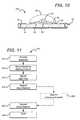
- FIG. 11shows one embodiment of a method 210 according to the present invention.
- the method 210is described with reference to an LED package, it is understood that the method can be used to fabricate other semiconductor device packages. It is further understood that although the method 210 is shown as a series of steps, the steps can occur in different order and different steps can be employed.
- a substrateis provided that can be any number of different substrates, but is preferably similar to the substrate 42 described above and shown in FIGS. 2-6 .
- a meniscus holding featureis mounted to the substrate using known mounting methods. Many different meniscus holding features can be used, including but not limited to the meniscus rings 24 , 52 , 72 , 92 , 108 , 122 , and 138 described above and shown in FIGS. 1-7 .
- the meniscus ringcan be formed as part of the substrate. It is also understood that more than one meniscus ring can be utilized in different embodiments including LED array embodiments.
- the meniscus forming “feature”may comprise a chemical, rather than or in addition to, a geometrical barrier such that the lens material does not tend to “wet” regions outside of the feature, thereby forming the meniscus.
- an LED chipis mounted to the substrate using known mounting methods such that an electric signal can be applied from the substrate to the LED chip.
- the electric signalis applied to the LED chip through at least one wire bond.
- the LED chipis preferably mounted inside the meniscus ring. In other embodiments multiple LED chips can be mounted to the substrate inside the meniscus ring, and for LED arrays, one or more LED chips can be mounted inside each of a plurality of meniscus rings.
- a soft inner materialis deposited in liquid form over and covering of the LED chip in a substantially hemispheric shape and is cured.
- the soft materialis included over each of the LED chips and cured, although in some embodiments less than all can be covered by the soft material.
- the wire bondis at least covered by said soft inner material.
- an inner (second) meniscus ring or meniscus holding featurecan be included around the LED chip to hold the soft inner material in its substantially hemispheric shape prior to curing.
- an adhesive materialcan be included on the substrate to hold the lens and compensate for CTE mismatches.
- a lens materialis included over the soft inner material in liquid form and then cured to state where it is harder than said inner material.
- the liquid lens materialis preferably held in a substantially hemispheric shape by the meniscus formed between the liquid and meniscus holding feature.
- the liquidis preferably held and in 224 it is cured in its hemispheric shape.
Landscapes
- Led Device Packages (AREA)
Abstract
Description
- (Sr,Ca,Ba) (Al,Ga)2S4:Eu2+
- Ba2(Mg, Zn) Si2O7:Eu2+
- Gd0.46Sr0.31Al1.23OxF1.38Eu2+0.06
- (Ba1-x-ySrxCay) SiO4:Eu
- Ba2SiO4:Eu2+
Red - Lu2O3:Eu3+
- (Sr2-xLax)(Ce1-xEux)O4
- Sr2Ce1-xEuxO4
- Sr2-xEuxCeO4
- SrTiO3:Pr3+,Ga3+
- CaAlSiN3:Eu2+
- Sr2Si5N8:Eu2+
Claims (42)
Priority Applications (1)
| Application Number | Priority Date | Filing Date | Title |
|---|---|---|---|
| US11/496,922US8735920B2 (en) | 2006-07-31 | 2006-07-31 | Light emitting diode package with optical element |
Applications Claiming Priority (1)
| Application Number | Priority Date | Filing Date | Title |
|---|---|---|---|
| US11/496,922US8735920B2 (en) | 2006-07-31 | 2006-07-31 | Light emitting diode package with optical element |
Publications (2)
| Publication Number | Publication Date |
|---|---|
| US20080023711A1 US20080023711A1 (en) | 2008-01-31 |
| US8735920B2true US8735920B2 (en) | 2014-05-27 |
Family
ID=38985274
Family Applications (1)
| Application Number | Title | Priority Date | Filing Date |
|---|---|---|---|
| US11/496,922ActiveUS8735920B2 (en) | 2006-07-31 | 2006-07-31 | Light emitting diode package with optical element |
Country Status (1)
| Country | Link |
|---|---|
| US (1) | US8735920B2 (en) |
Cited By (9)
| Publication number | Priority date | Publication date | Assignee | Title |
|---|---|---|---|---|
| US20140097452A1 (en)* | 2012-10-09 | 2014-04-10 | Sampei TOMOHIRO | Luminescence device |
| US20140179035A1 (en)* | 2012-12-26 | 2014-06-26 | Hon Hai Precision Industry Co., Ltd. | Method for dispensing glue on led chip |
| US20140217444A1 (en)* | 2011-06-20 | 2014-08-07 | Osram Opto Semiconductors Gmbh | Optoelectronic semiconductor component and method for the production thereof |
| US20140306253A1 (en)* | 2006-07-21 | 2014-10-16 | Epistar Corporation | Light Emitting Device |
| US20150372206A1 (en)* | 2011-09-20 | 2015-12-24 | Lg Innotek Co., Ltd. | Light emitting device package and lighting system including the same |
| US9691949B2 (en) | 2014-05-30 | 2017-06-27 | Cree, Inc. | Submount based light emitter components and methods |
| US10256385B2 (en) | 2007-10-31 | 2019-04-09 | Cree, Inc. | Light emitting die (LED) packages and related methods |
| US10957736B2 (en) | 2018-03-12 | 2021-03-23 | Cree, Inc. | Light emitting diode (LED) components and methods |
| US20220359802A1 (en)* | 2018-02-26 | 2022-11-10 | Semicon Light Co., Ltd. | Semiconductor light emitting devices and method of manufacturing the same |
Families Citing this family (53)
| Publication number | Priority date | Publication date | Assignee | Title |
|---|---|---|---|---|
| US8969908B2 (en)* | 2006-04-04 | 2015-03-03 | Cree, Inc. | Uniform emission LED package |
| KR100828900B1 (en)* | 2006-09-04 | 2008-05-09 | 엘지이노텍 주식회사 | Light emitting diode package and manufacturing method thereof |
| KR100845856B1 (en)* | 2006-12-21 | 2008-07-14 | 엘지전자 주식회사 | Light emitting device package and its manufacturing method |
| DE102007021904A1 (en)* | 2007-02-28 | 2008-09-04 | Osram Opto Semiconductors Gmbh | Housing body for opto-electronic component, has main surface with surface area and another surface area, and both surface areas are adjoined together by outer edge |
| US20090065792A1 (en)* | 2007-09-07 | 2009-03-12 | 3M Innovative Properties Company | Method of making an led device having a dome lens |
| TWI401820B (en)* | 2007-11-07 | 2013-07-11 | Ind Tech Res Inst | Light-emitting element and manufacturing method thereof |
| US8946987B2 (en)* | 2007-11-07 | 2015-02-03 | Industrial Technology Research Institute | Light emitting device and fabricating method thereof |
| TWI422058B (en)* | 2008-03-04 | 2014-01-01 | Everlight Electronics Co Ltd | Light-emitting diode package structure and manufacturing method thereof |
| DE102008025491A1 (en)* | 2008-05-28 | 2009-12-03 | Osram Opto Semiconductors Gmbh | Optoelectronic semiconductor component and printed circuit board |
| JP5512515B2 (en)* | 2008-05-30 | 2014-06-04 | シャープ株式会社 | Light emitting device, surface light source, and liquid crystal display device |
| JP2010010437A (en)* | 2008-06-27 | 2010-01-14 | Stanley Electric Co Ltd | Optical semiconductor device |
| US9252336B2 (en) | 2008-09-26 | 2016-02-02 | Bridgelux, Inc. | Multi-cup LED assembly |
| US8058664B2 (en)* | 2008-09-26 | 2011-11-15 | Bridgelux, Inc. | Transparent solder mask LED assembly |
| US8049236B2 (en)* | 2008-09-26 | 2011-11-01 | Bridgelux, Inc. | Non-global solder mask LED assembly |
| TWI403006B (en)* | 2009-01-15 | 2013-07-21 | Everlight Electronics Co Ltd | Light-emitting diode component package structure and manufacturing method thereof |
| KR101114592B1 (en)* | 2009-02-17 | 2012-03-09 | 엘지이노텍 주식회사 | Lighting emitting device and fabrication method thereof |
| US20100289055A1 (en)* | 2009-05-14 | 2010-11-18 | Avago Technologies Ecbu Ip (Singapore) Pte. Ltd. | Silicone leaded chip carrier |
| TWI403004B (en)* | 2009-09-04 | 2013-07-21 | Led package structure for increasing heat-dissipating effect and light-emitting efficiency and method for making the same | |
| JP5936810B2 (en)* | 2009-09-11 | 2016-06-22 | ローム株式会社 | Light emitting device |
| TWI403005B (en)* | 2009-10-12 | 2013-07-21 | Intematix Technology Ct Corp | Light-emitting diode and manufacturing method thereof |
| EP2323186B1 (en)* | 2009-11-13 | 2017-07-26 | Tridonic Jennersdorf GmbH | Light-emitting diode module and corresponding manufacturing method |
| DE102010029368A1 (en) | 2010-05-27 | 2011-12-01 | Osram Opto Semiconductors Gmbh | Electronic device and method for manufacturing an electronic device |
| DE102010045316A1 (en)* | 2010-09-14 | 2012-03-15 | Osram Opto Semiconductors Gmbh | Radiation-emitting component |
| JP5767062B2 (en)* | 2010-09-30 | 2015-08-19 | 日東電工株式会社 | Light emitting diode sealing material and method for manufacturing light emitting diode device |
| CN102064267A (en)* | 2010-11-02 | 2011-05-18 | 佛山市国星光电股份有限公司 | Light emitting diode (LED) support unit for display screen, LED support and method for manufacturing LED support unit |
| US20120248201A1 (en)* | 2011-01-31 | 2012-10-04 | American Bank Note Company | Dual-interface smart card |
| EP2671192A4 (en)* | 2011-01-31 | 2014-10-22 | American Bank Note Co | Dual-interface smart card |
| DE102011003969B4 (en) | 2011-02-11 | 2023-03-09 | OSRAM Opto Semiconductors Gesellschaft mit beschränkter Haftung | Process for producing an optoelectronic component |
| US11251164B2 (en)* | 2011-02-16 | 2022-02-15 | Creeled, Inc. | Multi-layer conversion material for down conversion in solid state lighting |
| US8373183B2 (en)* | 2011-02-22 | 2013-02-12 | Hong Kong Applied Science and Technology Research Institute Company Limited | LED package for uniform color emission |
| TW201240161A (en)* | 2011-03-17 | 2012-10-01 | Lextar Electronics Corp | Light emiting diode package structure and manufacturing method thereof |
| US10147853B2 (en) | 2011-03-18 | 2018-12-04 | Cree, Inc. | Encapsulant with index matched thixotropic agent |
| JP5962102B2 (en) | 2011-03-24 | 2016-08-03 | 日亜化学工業株式会社 | Light emitting device and manufacturing method thereof |
| KR20120119350A (en)* | 2011-04-21 | 2012-10-31 | 삼성전자주식회사 | Light emitting device module and method for manufacturing the same |
| US8746923B2 (en) | 2011-12-05 | 2014-06-10 | Cooledge Lighting Inc. | Control of luminous intensity distribution from an array of point light sources |
| JP5848114B2 (en)* | 2011-12-20 | 2016-01-27 | スタンレー電気株式会社 | Light emitting device |
| TWI590494B (en)* | 2012-02-14 | 2017-07-01 | 信越化學工業股份有限公司 | Optical semiconductor device package, its manufacturing method, and optical semiconductor device and its manufacturing method |
| DE102012208730A1 (en)* | 2012-05-24 | 2013-11-28 | Osram Opto Semiconductors Gmbh | Optoelectronic component device and method for producing an optoelectronic component device |
| CN105009314B (en)* | 2013-02-27 | 2019-11-05 | 日亚化学工业株式会社 | Light emitting device, light-emitting component installation method and light-emitting component mounting device |
| AT513747B1 (en) | 2013-02-28 | 2014-07-15 | Mikroelektronik Ges Mit Beschränkter Haftung Ab | Assembly process for circuit carriers and circuit carriers |
| US9799802B2 (en) | 2013-05-23 | 2017-10-24 | Lg Innotek Co., Ltd. | Light emitting module |
| US9608177B2 (en)* | 2013-08-27 | 2017-03-28 | Lumens Co., Ltd. | Light emitting device package and backlight unit having the same |
| JP6325471B2 (en)* | 2015-03-02 | 2018-05-16 | 株式会社東芝 | Optical coupling device and insulation device |
| JP6626294B2 (en)* | 2015-09-04 | 2019-12-25 | 株式会社東芝 | Semiconductor device and optical coupling device |
| CA3030017A1 (en)* | 2016-07-08 | 2018-01-11 | Eaton Intelligent Power Limited | Led light system having elastomeric encapsulation |
| JP6399057B2 (en)* | 2016-08-22 | 2018-10-03 | 日亜化学工業株式会社 | Light emitting device |
| DE102016125909A1 (en)* | 2016-12-30 | 2018-07-05 | Osram Opto Semiconductors Gmbh | Component and connection carrier |
| US10062817B1 (en)* | 2017-01-10 | 2018-08-28 | Rayvio Corporation | Ultraviolet emitting device with shaped encapsulant |
| US11257987B2 (en)* | 2017-10-16 | 2022-02-22 | PlayNitride Inc. | Structure with micro light-emitting device |
| JPWO2020045604A1 (en)* | 2018-08-31 | 2021-08-12 | パナソニックIpマネジメント株式会社 | Package for mounting semiconductor elements and semiconductor devices |
| US11600754B2 (en)* | 2018-11-29 | 2023-03-07 | Lumileds Llc | Light-emitting device and method of packaging the same |
| WO2020109023A1 (en)* | 2018-11-29 | 2020-06-04 | Lumileds Holding B.V. | Light-emitting device and method of packaging the same |
| CN111211209B (en)* | 2020-01-16 | 2021-09-28 | 江西新正耀光学研究院有限公司 | Ultraviolet light-emitting diode and manufacturing method thereof |
Citations (252)
| Publication number | Priority date | Publication date | Assignee | Title |
|---|---|---|---|---|
| US3760237A (en)* | 1972-06-21 | 1973-09-18 | Gen Electric | Solid state lamp assembly having conical light director |
| JPS53118019U (en) | 1977-02-28 | 1978-09-20 | ||
| JPS53126570U (en) | 1977-03-15 | 1978-10-07 | ||
| US4307297A (en) | 1978-09-12 | 1981-12-22 | U.S. Philips Corporation | Opto-electronic device |
| US4322735A (en) | 1979-05-11 | 1982-03-30 | Tokyo Shibaura Denki Kabushiki Kaisha | Display device |
| US4511425A (en)* | 1983-06-13 | 1985-04-16 | Dennison Manufacturing Company | Heated pad decorator |
| JPS62160564U (en) | 1986-03-31 | 1987-10-13 | ||
| US5040868A (en) | 1989-05-31 | 1991-08-20 | Siemens Aktiengesellschaft | Surface-mountable opto-component |
| US5042048A (en) | 1990-03-02 | 1991-08-20 | Meyer Brad E | Target illuminators and systems employing same |
| US5122943A (en) | 1991-04-15 | 1992-06-16 | Miles Inc. | Encapsulated light emitting diode and method for encapsulation |
| US5130761A (en) | 1990-07-17 | 1992-07-14 | Kabushiki Kaisha Toshiba | Led array with reflector and printed circuit board |
| US5167556A (en) | 1990-07-03 | 1992-12-01 | Siemens Aktiengesellschaft | Method for manufacturing a light emitting diode display means |
| US5351106A (en) | 1991-07-01 | 1994-09-27 | Amergraph Corporation | Exposure system |
| US5703401A (en) | 1995-05-10 | 1997-12-30 | U.S. Philips Corporation | Miniature semiconductor device for surface mounting |
| US5706177A (en) | 1994-12-24 | 1998-01-06 | Temic Telefunken Microelectronic Gmbh | Multi-terminal surface-mounted electronic device |
| US5731547A (en)* | 1996-02-20 | 1998-03-24 | International Business Machines Corporation | Circuitized substrate with material containment means and method of making same |
| US5790298A (en) | 1994-05-03 | 1998-08-04 | Gentex Corporation | Method of forming optically transparent seal and seal formed by said method |
| US5813753A (en) | 1997-05-27 | 1998-09-29 | Philips Electronics North America Corporation | UV/blue led-phosphor device with efficient conversion of UV/blues light to visible light |
| US5907151A (en) | 1996-05-24 | 1999-05-25 | Siemens Aktiengesellschaft | Surface mountable optoelectronic transducer and method for its production |
| US5942770A (en) | 1997-04-14 | 1999-08-24 | Rohm, Co., Ltd. | Light-emitting diode chip component and a light-emitting device |
| US5959316A (en) | 1998-09-01 | 1999-09-28 | Hewlett-Packard Company | Multiple encapsulation of phosphor-LED devices |
| US6061160A (en) | 1996-05-31 | 2000-05-09 | Dowa Mining Co., Ltd. | Component device for optical communication |
| US6066861A (en) | 1996-09-20 | 2000-05-23 | Siemens Aktiengesellschaft | Wavelength-converting casting composition and its use |
| EP1005085A2 (en) | 1998-11-19 | 2000-05-31 | Matsushita Electronics Corporation | Resin-encapsulated electronic device |
| JP2000188358A (en) | 1998-12-22 | 2000-07-04 | Rohm Co Ltd | Semiconductor device |
| JP2000223752A (en) | 1999-01-29 | 2000-08-11 | Nichia Chem Ind Ltd | Optical semiconductor device and its forming method |
| JP2000223751A (en) | 1998-11-25 | 2000-08-11 | Nichia Chem Ind Ltd | Led lamp and display device using the led lamp |
| JP2000261041A (en) | 1999-03-04 | 2000-09-22 | Citizen Electronics Co Ltd | Surface-mounting type light emitting diode and manufacture of the same |
| CN1274906A (en) | 1999-05-24 | 2000-11-29 | 索尼公司 | Two-dimensional display device |
| US6183100B1 (en) | 1997-10-17 | 2001-02-06 | Truck-Lite Co., Inc. | Light emitting diode 360° warning lamp |
| JP2001044506A (en) | 1999-07-26 | 2001-02-16 | Ichikoh Ind Ltd | Light emitting diode fixing structure |
| US6224216B1 (en) | 2000-02-18 | 2001-05-01 | Infocus Corporation | System and method employing LED light sources for a projection display |
| JP2001168400A (en) | 1999-12-09 | 2001-06-22 | Rohm Co Ltd | Chip type light emitting device with case and method of manufacturing the same |
| US6259608B1 (en) | 1999-04-05 | 2001-07-10 | Delphi Technologies, Inc. | Conductor pattern for surface mount devices and method therefor |
| US6274924B1 (en) | 1998-11-05 | 2001-08-14 | Lumileds Lighting, U.S. Llc | Surface mountable LED package |
| JP2001237463A (en) | 2000-02-24 | 2001-08-31 | Matsushita Electric Works Ltd | Led module |
| US6296367B1 (en) | 1999-10-15 | 2001-10-02 | Armament Systems And Procedures, Inc. | Rechargeable flashlight with step-up voltage converter and recharger therefor |
| JP2001518692A (en) | 1997-07-29 | 2001-10-16 | オスラム オプト セミコンダクターズ ゲゼルシャフト ミット ベシュレンクテル ハフツング ウント コンパニー オッフェネ ハンデルスゲゼルシャフト | Photoelectric element |
| JP2002009217A (en) | 2000-06-23 | 2002-01-11 | Fuji Electric Co Ltd | Resin-sealed semiconductor device |
| US20020021085A1 (en) | 2000-08-09 | 2002-02-21 | Ng Kee Yean | Light emitting devices |
| EP1187226A1 (en) | 2000-09-01 | 2002-03-13 | Citizen Electronics Co., Ltd. | Surface-mount type light emitting diode and method of manufacturing same |
| US20020030194A1 (en) | 2000-09-12 | 2002-03-14 | Camras Michael D. | Light emitting diodes with improved light extraction efficiency |
| US6359236B1 (en) | 1992-07-24 | 2002-03-19 | Tessera, Inc. | Mounting component with leads having polymeric strips |
| US20020061174A1 (en) | 2000-01-21 | 2002-05-23 | Hans Hurt | Electro-optical data transfer module |
| US20020066905A1 (en) | 2000-06-20 | 2002-06-06 | Bily Wang | Wing-shaped surface mount package for light emitting diodes |
| CN2498694Y (en) | 2001-08-14 | 2002-07-03 | 北京利亚德电子科技有限公司 | Inclined LED image module |
| JP2002223005A (en) | 2001-01-26 | 2002-08-09 | Toyoda Gosei Co Ltd | Light emitting diode and display device |
| US20020123163A1 (en) | 2000-04-24 | 2002-09-05 | Takehiro Fujii | Edge-emitting light-emitting semiconductor device and method of manufacture thereof |
| US6447124B1 (en) | 1996-03-19 | 2002-09-10 | Donnelly Mirrors Limited | Electro-optic rearview mirror system |
| US6454437B1 (en) | 1999-07-28 | 2002-09-24 | William Kelly | Ring lighting |
| US20020163001A1 (en) | 2001-05-04 | 2002-11-07 | Shaddock David Mulford | Surface mount light emitting device package and fabrication method |
| US6480389B1 (en) | 2002-01-04 | 2002-11-12 | Opto Tech Corporation | Heat dissipation structure for solid-state light emitting device package |
| US20020171911A1 (en) | 2001-05-17 | 2002-11-21 | Mamoru Maegawa | Method for adjusting the hue of the light emitted by a light-emitting diode |
| US20020195935A1 (en) | 1999-12-30 | 2002-12-26 | Harald Jager | Surface-mountable light-emitting diode light source and method of producing a light-emitting diode light source |
| JP2002374005A (en) | 2001-04-10 | 2002-12-26 | Toshiba Corp | Optical semiconductor device |
| US6517218B2 (en) | 2000-03-31 | 2003-02-11 | Relume Corporation | LED integrated heat sink |
| US20030116769A1 (en) | 2001-12-24 | 2003-06-26 | Samsung Electro-Mechanics Co., Ltd. | Light emission diode package |
| US6610563B1 (en) | 1997-12-15 | 2003-08-26 | Osram Opto Semiconductors Gmbh & Co. Ohg | Surface mounting optoelectronic component and method for producing same |
| US20030160256A1 (en) | 2000-09-01 | 2003-08-28 | General Electric Company | Plastic packaging of LED arrays |
| US6614058B2 (en) | 2001-07-12 | 2003-09-02 | Highlink Technology Corporation | Light emitting semiconductor device with a surface-mounted and flip-chip package structure |
| US6621210B2 (en) | 2000-07-14 | 2003-09-16 | Sony Corporation | Front plate for field-emission display comprising barriers formed of conductive inorganic material |
| JP2003264267A (en) | 2002-03-08 | 2003-09-19 | Rohm Co Ltd | Semiconductor device using semiconductor chip |
| US6624491B2 (en) | 1998-06-30 | 2003-09-23 | Osram Opto Semiconductors Gmbh & Co. | Diode housing |
| US20030183852A1 (en) | 2002-03-20 | 2003-10-02 | Sharp Kabushiki Kaisha | Light emitting device and manufacturing method thereof |
| JP2003318449A (en) | 2003-05-20 | 2003-11-07 | Sanyo Electric Co Ltd | Led light source and its fabricating method |
| WO2004003660A1 (en) | 2002-07-01 | 2004-01-08 | Bård Eker Industrial Design As | Projector |
| US6680490B2 (en) | 2001-06-15 | 2004-01-20 | Toyoda Gosei Co., Ltd. | Light-emitting device |
| JP2004022862A (en) | 2002-06-18 | 2004-01-22 | Rohm Co Ltd | Semiconductor device |
| US20040016938A1 (en) | 1996-03-26 | 2004-01-29 | Bruce Baretz | Solid state white light emitter and display using same |
| US6686609B1 (en) | 2002-10-01 | 2004-02-03 | Ultrastar Limited | Package structure of surface mounting led and method of manufacturing the same |
| JP2004056075A (en) | 2002-05-31 | 2004-02-19 | Stanley Electric Co Ltd | Light emitting device and manufacturing method thereof |
| US20040037076A1 (en) | 2002-07-17 | 2004-02-26 | Sharp Kabushiki Kaisha | Light emitting diode lamp and light emitting diode display unit |
| US6700136B2 (en) | 2001-07-30 | 2004-03-02 | General Electric Company | Light emitting device package |
| US20040041222A1 (en) | 2002-09-04 | 2004-03-04 | Loh Ban P. | Power surface mount light emitting die package |
| JP2004507114A (en) | 2000-08-23 | 2004-03-04 | オスラム オプト セミコンダクターズ ゲゼルシャフト ミット ベシュレンクテル ハフツング | Optoelectronic component, method of manufacturing the same, module with a plurality of optoelectronic components, and device with such a module |
| US6710373B2 (en) | 1999-09-27 | 2004-03-23 | Shih-Yi Wang | Means for mounting photoelectric sensing elements, light emitting diodes, or the like |
| JP2004103775A (en) | 2002-09-09 | 2004-04-02 | Eeshikku Kk | Chip led light emitting body and method for manufacturing the same |
| US6717353B1 (en)* | 2002-10-14 | 2004-04-06 | Lumileds Lighting U.S., Llc | Phosphor converted light emitting device |
| JP2004111937A (en) | 2002-08-30 | 2004-04-08 | Nichia Chem Ind Ltd | Light emitting device |
| US20040080939A1 (en) | 2001-04-23 | 2004-04-29 | Jules Braddell | Illuminator |
| US20040079957A1 (en) | 2002-09-04 | 2004-04-29 | Andrews Peter Scott | Power surface mount light emitting die package |
| EP1418630A1 (en) | 2002-11-07 | 2004-05-12 | Matsushita Electric Industrial Co., Ltd. | LED lamp |
| CN2617039Y (en) | 2003-02-21 | 2004-05-19 | 游尚桦 | Adhesive LED lead frame |
| JP2004146815A (en) | 2002-09-30 | 2004-05-20 | Sanyo Electric Co Ltd | Light emitting device |
| WO2004053933A2 (en) | 2002-12-06 | 2004-06-24 | Cree, Inc. | Composite leadframe led package and method of making the same |
| JP2004200236A (en) | 2002-12-16 | 2004-07-15 | Matsushita Electric Ind Co Ltd | Light emitting diode display |
| US6765801B1 (en)* | 2001-06-25 | 2004-07-20 | Amkor Technology, Inc. | Optical track drain package |
| US6765235B2 (en) | 2002-02-27 | 2004-07-20 | Oki Data Corporation | Array of semiconductor elements with paired driving scheme |
| US6770498B2 (en) | 2002-06-26 | 2004-08-03 | Lingsen Precision Industries, Ltd. | LED package and the process making the same |
| US6774401B2 (en) | 2002-07-12 | 2004-08-10 | Stanley Electric Co., Ltd. | Light emitting diode |
| JP2004228387A (en) | 2003-01-23 | 2004-08-12 | Koha Co Ltd | Light emitting device |
| US6791259B1 (en) | 1998-11-30 | 2004-09-14 | General Electric Company | Solid state illumination system containing a light emitting diode, a light scattering material and a luminescent material |
| CN2646873Y (en) | 2003-10-16 | 2004-10-06 | 上海三思科技发展有限公司 | A surface sticking type LED with tilted light axis |
| US20040217364A1 (en) | 2003-05-01 | 2004-11-04 | Cree Lighting Company, Inc. | Multiple component solid state white light |
| US20040227149A1 (en)* | 2003-04-30 | 2004-11-18 | Cree, Inc. | High powered light emitter packages with compact optics |
| JP2004335880A (en) | 2003-05-09 | 2004-11-25 | Toshiba Lighting & Technology Corp | Light emitting device |
| US20040232435A1 (en) | 2003-02-28 | 2004-11-25 | Osram Opto Semiconductors Gmbh | Optoelectronic device with patterned-metallized package body, method for producing such a device and method for the patterned metallization of a plastic-containing body |
| JP2004335740A (en) | 2003-05-07 | 2004-11-25 | Citizen Electronics Co Ltd | Light emitting diode and its package structure |
| US20040256706A1 (en) | 2003-06-20 | 2004-12-23 | Shintaro Nakashima | Molded package and semiconductor device using molded package |
| JP2005019838A (en) | 2003-06-27 | 2005-01-20 | Nippon Leiz Co Ltd | Light source device and method for manufacturing the same |
| US20050023548A1 (en) | 2003-07-31 | 2005-02-03 | Bhat Jerome C. | Mount for semiconductor light emitting device |
| CN1581527A (en) | 2003-08-13 | 2005-02-16 | 西铁城电子股份有限公司 | Luminous diode |
| CN1591924A (en) | 2003-07-29 | 2005-03-09 | 西铁城电子股份有限公司 | Surface-mounted LED and light emitting device with same |
| JP2005079167A (en) | 2003-08-28 | 2005-03-24 | Kyocera Corp | Light emitting element storage package and light emitting device |
| US6872585B2 (en) | 2001-09-03 | 2005-03-29 | Toyoda Gosei Co., Ltd. | LED device and manufacturing method thereof |
| US6876149B2 (en) | 2002-01-31 | 2005-04-05 | Citizen Electronics Co., Ltd. | Double-face LED device for an electronic instrument |
| EP1521313A2 (en) | 2003-10-03 | 2005-04-06 | LumiLeds Lighting U.S., LLC | Integrated reflector cup for a light emitting device mount |
| US20050072981A1 (en)* | 2002-02-19 | 2005-04-07 | Ryoma Suenaga | Light-emitting device and process for producing thereof |
| US20050077535A1 (en) | 2003-10-08 | 2005-04-14 | Joinscan Electronics Co., Ltd | LED and its manufacturing process |
| US20050093005A1 (en) | 2002-06-28 | 2005-05-05 | Osram Opto Semiconductors Gmbh | Optoelectronic component and method for producing it |
| US20050093430A1 (en)* | 2003-02-26 | 2005-05-05 | Cree, Inc. | Composite white light source and method for fabricating |
| US20050110033A1 (en) | 1998-07-28 | 2005-05-26 | Paul Heremans | High-efficiency radiating device |
| US20050117320A1 (en) | 2003-11-14 | 2005-06-02 | Hon Hai Precision Industry Co., Ltd. | Light-emitting diode and backlight system using the same |
| EP1538680A2 (en) | 2003-12-03 | 2005-06-08 | Sumitomo Electric Industries, Ltd. | Light emitting device |
| JP2005150624A (en) | 2003-11-19 | 2005-06-09 | Matsushita Electric Ind Co Ltd | Lead frame for semiconductor device and surface light emitting device using the same |
| US20050127377A1 (en) | 2001-11-30 | 2005-06-16 | Karlheinz Arndt | Optoelectronic component |
| US20050135105A1 (en) | 2003-12-19 | 2005-06-23 | Lumileds Lighting U.S., Llc | LED package assembly |
| US6911678B2 (en) | 2003-05-30 | 2005-06-28 | Stanley Electric Co., Ltd. | Glass-sealed light-emitting diode |
| US6914268B2 (en) | 2003-07-24 | 2005-07-05 | South Epitaxy Corporation | LED device, flip-chip LED package and light reflecting structure |
| US20050152127A1 (en) | 2003-12-19 | 2005-07-14 | Takayuki Kamiya | LED lamp apparatus |
| US20050156187A1 (en) | 2002-03-08 | 2005-07-21 | Shinji Isokawa | Semiconductor device using semiconductor chip |
| US20050179041A1 (en) | 2004-02-18 | 2005-08-18 | Lumileds Lighting U.S., Llc | Illumination system with LEDs |
| US20050179376A1 (en) | 2004-02-13 | 2005-08-18 | Fung Elizabeth C.L. | Light emitting diode display device |
| JP2003324214A5 (en) | 2002-04-30 | 2005-08-25 | ||
| US6940704B2 (en) | 2001-01-24 | 2005-09-06 | Gelcore, Llc | Semiconductor light emitting device |
| US20050199899A1 (en) | 2004-03-11 | 2005-09-15 | Ming-Der Lin | Package array and package unit of flip chip LED |
| US20050231983A1 (en) | 2002-08-23 | 2005-10-20 | Dahm Jonathan S | Method and apparatus for using light emitting diodes |
| WO2005104247A1 (en) | 2004-04-19 | 2005-11-03 | Matsushita Electric Industrial Co., Ltd. | Method for fabricating led illumination light source and led illumination light source |
| JP2005310935A (en) | 2004-04-20 | 2005-11-04 | Sumitomo Metal Electronics Devices Inc | Storing package for light-emitting element |
| US6964877B2 (en) | 2003-03-28 | 2005-11-15 | Gelcore, Llc | LED power package |
| US20050253130A1 (en) | 2004-03-26 | 2005-11-17 | Koito Manufacturing Co., Ltd. | Light source module and vehicle front lamp |
| US6975011B2 (en) | 1995-09-29 | 2005-12-13 | Osram Gmbh | Optoelectronic semiconductor component having multiple external connections |
| JP2005347401A (en) | 2004-06-01 | 2005-12-15 | Meiko:Kk | Optical element chip component |
| JP2005539386A (en) | 2002-09-17 | 2005-12-22 | オスラム オプト セミコンダクターズ ゲゼルシャフト ミット ベシュレンクテル ハフツング | Lead frame based housing, surface mountable photoelectric component and manufacturing method |
| JP2006019557A (en) | 2004-07-02 | 2006-01-19 | Fujikura Ltd | LIGHT EMITTING DEVICE AND ITS MOUNTING METHOD, LIGHTING APPARATUS AND DISPLAY |
| US6995510B2 (en) | 2001-12-07 | 2006-02-07 | Hitachi Cable, Ltd. | Light-emitting unit and method for producing same as well as lead frame used for producing light-emitting unit |
| WO2006016398A1 (en) | 2004-08-10 | 2006-02-16 | Renesas Technology Corp. | Light emitting device and process for manufacturing the same |
| US7009627B2 (en) | 2001-11-21 | 2006-03-07 | Canon Kabushiki Kaisha | Display apparatus, and image signal processing apparatus and drive control apparatus for the same |
| CN1744335A (en) | 2004-08-31 | 2006-03-08 | 斯坦雷电气株式会社 | Surface Mount LEDs |
| US20060049477A1 (en) | 2002-11-29 | 2006-03-09 | Karlheinz Arndt | Optoelectronic component |
| USD517025S1 (en) | 2003-03-17 | 2006-03-14 | Nichia Corporation | Light emitting diode |
| US20060060867A1 (en) | 2004-09-09 | 2006-03-23 | Toyoda Gosei Co., Ltd. | Light emitting device |
| US7021797B2 (en) | 2003-05-13 | 2006-04-04 | Light Prescriptions Innovators, Llc | Optical device for repositioning and redistributing an LED's light |
| JP2006108517A (en) | 2004-10-08 | 2006-04-20 | Citizen Watch Co Ltd | Substrate for led connection, illuminator using thereof, and display device using thereof |
| EP1653254A2 (en) | 2004-10-18 | 2006-05-03 | Samsung Electronics Co., Ltd. | Light emitting diode and lens for the same |
| US20060091406A1 (en) | 2004-11-04 | 2006-05-04 | Hiroki Kaneko | Illuminating apparatus, method for fabricating the same and display apparatus using the same |
| JP2006119357A (en) | 2004-10-21 | 2006-05-11 | Koha Co Ltd | Display device |
| GB2420221A (en) | 2004-11-12 | 2006-05-17 | Unity Opto Technology Co Ltd | Semiconductor light emitting diode package with heat sink |
| US20060102917A1 (en) | 2002-06-19 | 2006-05-18 | Toshihiko Oyama | Semiconductor light emitting device, method for producing the same and reflector for semiconductor light emitting device |
| US20060108594A1 (en)* | 2004-11-11 | 2006-05-25 | Kazuyuki Iwasaki | LED device and method for manufacturing the same |
| WO2006054228A2 (en) | 2004-11-18 | 2006-05-26 | Koninklijke Philips Electronics N.V. | Illuminator and method for producing such illuminator |
| US7064907B2 (en) | 2003-06-12 | 2006-06-20 | Seiko Epson Corporation | Optical part and its manufacturing method |
| US20060131591A1 (en) | 2004-12-16 | 2006-06-22 | Naofumi Sumitani | Light emitting apparatus |
| US20060133044A1 (en) | 2004-12-16 | 2006-06-22 | Seoul Semiconductor Co., Ltd. | Leadframe and packaged light emitting diode |
| US7066626B2 (en) | 2003-04-09 | 2006-06-27 | Citizen Electronics Co., Ltd. | LED lamp |
| CN1801498A (en) | 2005-01-07 | 2006-07-12 | 北京大学 | Preparation method of LED chip with discrete grain vertical structure |
| US20060151809A1 (en) | 2003-06-03 | 2006-07-13 | Rohm Co., Ltd | Optical semiconductor unit |
| US20060220046A1 (en) | 2005-03-04 | 2006-10-05 | Chuan-Pei Yu | Led |
| US7119422B2 (en) | 2004-11-15 | 2006-10-10 | Unity Opto Technology Co., Ltd. | Solid-state semiconductor light emitting device |
| JP2006324331A (en) | 2005-05-17 | 2006-11-30 | Sony Corp | Light emitting diode and its manufacturing method, integrated light emitting diode and its manufacturing method, growing method of nitride- based group iii-v compound semiconductor, nitride-based group iii-v compound semiconductor growing substrate, light emitting diode backlight, light emitting diode lighting apparatus, light emitting diode display, and electronic equipment |
| US20060267042A1 (en) | 2001-10-12 | 2006-11-30 | Nichia Corporation | Light emitting apparatus and method of manufacturing the same |
| CN1874011A (en) | 2005-06-03 | 2006-12-06 | 邢陈震仑 | A light emitting diode device |
| US20060278882A1 (en) | 2005-06-10 | 2006-12-14 | Cree, Inc. | Power lamp package |
| JP2006344692A (en) | 2005-06-07 | 2006-12-21 | Fujikura Ltd | Light emitting element mounting substrate and light emitting element module |
| WO2006135502A1 (en) | 2005-06-10 | 2006-12-21 | Cree, Inc. | High power solid-state lamp |
| US20060291185A1 (en) | 2005-06-28 | 2006-12-28 | Sato Atsushi | Planar light source device and display using the same |
| US7161189B2 (en) | 2004-06-04 | 2007-01-09 | Lite-On Technology Corporation | LED package including a frame |
| CN1913135A (en) | 2005-08-11 | 2007-02-14 | 安华高科技Ecbuip(新加坡)私人有限公司 | PLCC package with integrated lens and method for making the package |
| US20070046176A1 (en) | 2005-04-27 | 2007-03-01 | Spudnik,Inc. | Phosphor Compositions For Scanning Beam Displays |
| US7187009B2 (en) | 2001-06-12 | 2007-03-06 | Citizen Electronics Co., Ltd. | Light emitting diode device for illumination objects |
| EP1187228A4 (en) | 2000-02-09 | 2007-03-07 | Nippon Leiz Corp | LIGHT SOURCE |
| JP2007094088A (en) | 2005-09-29 | 2007-04-12 | Matsushita Electric Ind Co Ltd | Display device |
| US20070096139A1 (en) | 2005-11-02 | 2007-05-03 | 3M Innovative Properties Company | Light emitting diode encapsulation shape control |
| US20070109779A1 (en) | 2005-11-11 | 2007-05-17 | Yoshifumi Sekiguchi | Illuminating device and liquid-crystal display device using the same |
| US7224000B2 (en) | 2002-08-30 | 2007-05-29 | Lumination, Llc | Light emitting diode component |
| CN1977399A (en) | 2005-04-01 | 2007-06-06 | 松下电器产业株式会社 | LED component and method for manufacturing same |
| JP2007165029A (en) | 2005-12-12 | 2007-06-28 | Hitachi Displays Ltd | Display device |
| JP2007165840A (en) | 2005-09-09 | 2007-06-28 | Matsushita Electric Works Ltd | Light-emitting device |
| US20070145401A1 (en) | 2005-12-27 | 2007-06-28 | Sharp Kabushiki Kaisha | Semiconductor light emitting device, semiconductor element, and method for fabricating the semiconductor light emitting device |
| JP2007184542A (en) | 2005-12-09 | 2007-07-19 | Matsushita Electric Ind Co Ltd | LIGHT EMITTING MODULE, ITS MANUFACTURING METHOD, AND BACKLIGHT DEVICE USING THE SAME |
| CN101005109A (en) | 2006-01-16 | 2007-07-25 | 榎本股份有限公司 | Low height lead frame for LED device and the manufacturing method thereof |
| US20070170449A1 (en) | 2006-01-24 | 2007-07-26 | Munisamy Anandan | Color sensor integrated light emitting diode for LED backlight |
| WO2007083408A1 (en) | 2006-01-20 | 2007-07-26 | Sharp Kabushiki Kaisha | Light source unit, lighting apparatus using the light source unit, and display using the lighting apparatus |
| CN101013689A (en) | 2007-01-30 | 2007-08-08 | 深圳市共达光电器件有限公司 | LED packaging structure and packaging method |
| JP2007243226A (en) | 2007-06-20 | 2007-09-20 | Sony Corp | Light source apparatus and display apparatus |
| US7282740B2 (en) | 2003-12-17 | 2007-10-16 | Sharp Kabushiki Kaisha | Semiconductor light emitting device |
| JP2007273763A (en) | 2006-03-31 | 2007-10-18 | Sony Corp | Semiconductor device and its manufacturing method |
| US20070241357A1 (en) | 2004-10-29 | 2007-10-18 | Ledengin, Inc. | LED packages with mushroom shaped lenses and methods of manufacturing LED light-emitting devices |
| US7285802B2 (en) | 2004-12-21 | 2007-10-23 | 3M Innovative Properties Company | Illumination assembly and method of making same |
| WO2007121486A2 (en) | 2006-04-18 | 2007-10-25 | Lamina Lighting, Inc. | Optical devices for controlled color mixing |
| JP2007287981A (en) | 2006-04-18 | 2007-11-01 | Konica Minolta Opto Inc | Light emitting device |
| WO2007127029A2 (en) | 2006-04-24 | 2007-11-08 | Cree, Inc. | Side-view surface mount white led |
| JP2007299905A (en) | 2006-04-28 | 2007-11-15 | Nichia Chem Ind Ltd | Semiconductor device |
| US20070262328A1 (en) | 2006-05-10 | 2007-11-15 | Nichia Corporation | Semiconductor light emitting device and a method for producing the same |
| US20070269586A1 (en) | 2006-05-17 | 2007-11-22 | 3M Innovative Properties Company | Method of making light emitting device with silicon-containing composition |
| US7303315B2 (en) | 2004-11-05 | 2007-12-04 | 3M Innovative Properties Company | Illumination assembly using circuitized strips |
| JP2007317896A (en) | 2006-05-26 | 2007-12-06 | Nichia Chem Ind Ltd | Light emitting diode |
| JP2007329516A (en) | 2007-09-14 | 2007-12-20 | Sharp Corp | Semiconductor light emitting device |
| US20070295975A1 (en) | 2004-06-25 | 2007-12-27 | Sanyo Electric Co., Ltd. | Light-Emitting Device |
| US20080013319A1 (en) | 2006-07-13 | 2008-01-17 | Everlight Electronics Co., Ltd. | Light emitting diode package |
| US20080026498A1 (en) | 2006-07-31 | 2008-01-31 | Eric Tarsa | Light emitting diode package element with internal meniscus for bubble free lens placement |
| DE202007012162U1 (en) | 2007-06-05 | 2008-03-20 | Seoul Semiconductor Co., Ltd. | LED housing |
| US20080093606A1 (en) | 2006-10-24 | 2008-04-24 | Chipmos Technologies Inc. | Light emitting chip package and manufacturing method thereof |
| US20080121921A1 (en) | 2006-07-13 | 2008-05-29 | Cree, Inc. | Leadframe-based packages for solid state light emitting devices and methods of forming leadframe-based packages for solid state light emitting devices |
| US20080149960A1 (en) | 2006-12-26 | 2008-06-26 | Nichia Corporation | Light-emitting apparatus and method of producing the same |
| USD572210S1 (en) | 2006-11-01 | 2008-07-01 | Lg Innotek Co., Ltd. | Light-emitting diode (LED) |
| USD572670S1 (en) | 2006-03-30 | 2008-07-08 | Nichia Corporation | Light emitting diode |
| WO2008081794A1 (en) | 2006-12-28 | 2008-07-10 | Nichia Corporation | Light emitting device and method for manufacturing the same |
| WO2008082098A1 (en) | 2006-12-28 | 2008-07-10 | Seoul Semiconductor Co., Ltd. | Light emitting diode package |
| US20080170391A1 (en) | 2007-01-12 | 2008-07-17 | Aizar Abdul Karim Norfidathul | Multi-chip Packaged LED Light Source |
| EP1953834A1 (en) | 2005-11-21 | 2008-08-06 | Matsushita Electric Works, Ltd. | Light-emitting device |
| US20080186702A1 (en) | 2004-11-12 | 2008-08-07 | Lumileds Lighting U.S., Llc | Array of Light Emitting Devices to Produce a White Light Source |
| US20080191232A1 (en) | 2005-08-01 | 2008-08-14 | Seoul Semiconductor Co., Ltd. | Light Emitting Device With A Lens Of Silicone |
| US20080198594A1 (en) | 2006-12-19 | 2008-08-21 | Lee Sungkeun | Optical module |
| USD576574S1 (en) | 2007-07-17 | 2008-09-09 | Rohm Co., Ltd. | Light emitting diode module |
| US20080230790A1 (en) | 2007-03-23 | 2008-09-25 | Sharp Kabushiki Kaisha | Semiconductor light emitting device |
| US20080258156A1 (en) | 2006-09-29 | 2008-10-23 | Sanyo Electric Co., Ltd. | Light-emitting diode apparatus |
| US20080296590A1 (en) | 2007-05-31 | 2008-12-04 | Kee Yean Ng | LED-Based Light Source Having Improved Thermal Dissipation |
| US20080303052A1 (en) | 2004-09-10 | 2008-12-11 | Seoul Semiconductor Co., Ltd. | Light emitting diode package having multiple molding resins |
| US20080308825A1 (en) | 2007-06-14 | 2008-12-18 | Cree, Inc. | Encapsulant with scatterer to tailor spatial emission pattern and color uniformity in light emitting diodes |
| CN101360368A (en) | 2007-07-30 | 2009-02-04 | 深圳莱特光电有限公司 | Silver layer insulation method in warm white light LED encapsulation process |
| US20090050911A1 (en) | 2007-08-24 | 2009-02-26 | Cree, Inc. | Light emitting device packages using light scattering particles of different size |
| US20090050908A1 (en) | 2005-01-10 | 2009-02-26 | Cree, Inc. | Solid state lighting component |
| US20090057699A1 (en) | 2007-09-04 | 2009-03-05 | Philips Lumileds Lighting Company, Llc | LED with Particles in Encapsulant for Increased Light Extraction and Non-Yellow Off-State Color |
| US20090057708A1 (en) | 2007-08-27 | 2009-03-05 | Norfidathul Aizar Abdul Karim | LED Light Source Having Improved Resistance to Thermal Cycling |
| US20090072251A1 (en) | 2007-09-14 | 2009-03-19 | Cotco Luminant Device Limited | LED surface-mount device and LED display incorporating such device |
| US20090095966A1 (en) | 2007-10-10 | 2009-04-16 | Cree, Inc. | Multiple conversion material light emitting diode package and method of fabricating same |
| US20090129085A1 (en) | 2007-11-16 | 2009-05-21 | Avago Technologies Ecbu Ip (Singapore) Pte. Ltd. | Optical device |
| WO2009074919A1 (en) | 2007-12-11 | 2009-06-18 | Koninklijke Philips Electronics N.V. | Side emitting device with hybrid top reflector |
| US20090189178A1 (en) | 2006-06-30 | 2009-07-30 | Do Hyung Kim | Leadframe having a heat sink supporting part, fabricating method of a light emitting diode package using the same, and light emitting diode package fabricated by the method |
| US7579628B2 (en) | 2004-10-18 | 2009-08-25 | Sharp Kabushiki Kaisha | Backlight device for liquid crystal display including a plurality of light emitting diodes within their own concaves aligned in a straight line within a larger concave |
| GB2458972A (en) | 2008-08-05 | 2009-10-07 | Photonstar Led Ltd | Thermally optimized chip-on-board module |
| US20090283781A1 (en) | 2008-05-16 | 2009-11-19 | Cree Hong Kong Limited | Mini V SMD |
| US7622795B2 (en) | 2007-05-15 | 2009-11-24 | Nichepac Technology Inc. | Light emitting diode package |
| US7635915B2 (en) | 2006-04-26 | 2009-12-22 | Cree Hong Kong Limited | Apparatus and method for use in mounting electronic elements |
| WO2010005294A1 (en) | 2008-06-15 | 2010-01-14 | Stichting Administratiekantoor Vomgroup | A method for manufacturing a lens to be added to a led, and a lens obtained with that method |
| US20100044735A1 (en) | 2008-08-25 | 2010-02-25 | Citizen Electronics Co., Ltd. | Light-emitting device |
| US20100103660A1 (en) | 2008-10-24 | 2010-04-29 | Cree Led Lighting Solutions, Inc. | Array layout for color mixing |
| EP1864780B1 (en) | 2006-06-09 | 2010-05-26 | LG Electronics Inc. | Apparatus and method for manufacturing a light emitting unit |
| GB2466633A (en) | 2008-12-12 | 2010-07-07 | Glory Science Co Ltd | Method of manufacturing a light emitting unit |
| US20100193822A1 (en) | 2009-01-30 | 2010-08-05 | Nichia Corporation | Light emitting semiconductor device and method of manufacture thereof |
| US7777412B2 (en) | 2007-03-22 | 2010-08-17 | Avago Technologies Ecbu Ip (Singapore) Pte. Ltd. | Phosphor converted LED with improved uniformity and having lower phosphor requirements |
| US7847302B2 (en)* | 2005-08-26 | 2010-12-07 | Koninklijke Philips Electronics, N.V. | Blue LED with phosphor layer for producing white light and different phosphor in outer lens for reducing color temperature |
| US7875899B2 (en) | 2007-01-15 | 2011-01-25 | Showa Denko K.K. | Light-emitting diode package and lead group structure for light-emitting diode package |
| US20110049545A1 (en) | 2009-09-02 | 2011-03-03 | Koninklijke Philips Electronics N.V. | Led package with phosphor plate and reflective substrate |
| US20110108674A1 (en) | 2009-11-10 | 2011-05-12 | Cessna Aircraft Company | Cockpit Rudder Control Mechanism For An Aircraft |
| US20110186880A1 (en) | 2007-08-30 | 2011-08-04 | Osram Opto Semiconductors Gmbh | LED Housing |
| US20110193118A1 (en) | 2010-02-09 | 2011-08-11 | Oshima Yukitoyo | Light emitting device and manufacturing method thereof |
| US20110278617A1 (en) | 2010-05-12 | 2011-11-17 | Lee Gun Kyo | Light emitting device package |
| US8217414B2 (en) | 2006-12-28 | 2012-07-10 | Nichia Corporation | Light emitting device, package, light emitting device manufacturing method, package manufacturing method and package manufacturing die |
| WO2012099145A1 (en) | 2011-01-20 | 2012-07-26 | シャープ株式会社 | Light emitting device, lighting device, display device, and method for manufacturing light emitting device |
| US20120257386A1 (en) | 2011-06-24 | 2012-10-11 | Xicato, Inc. | Led based illumination module with a reflective mask |
Family Cites Families (3)
| Publication number | Priority date | Publication date | Assignee | Title |
|---|---|---|---|---|
| JP2003324214A (en) | 2002-04-30 | 2003-11-14 | Omron Corp | Light emitting module |
| JP5078480B2 (en)* | 2007-07-23 | 2012-11-21 | キヤノン株式会社 | Image processing apparatus and method, and computer program and recording medium |
| WO2011057102A1 (en)* | 2009-11-05 | 2011-05-12 | Luminit Llc | Method to Provide Microstructure for Encapsulated High-Brightness Led Chips |
- 2006
- 2006-07-31USUS11/496,922patent/US8735920B2/enactiveActive
Patent Citations (284)
| Publication number | Priority date | Publication date | Assignee | Title |
|---|---|---|---|---|
| US3760237A (en)* | 1972-06-21 | 1973-09-18 | Gen Electric | Solid state lamp assembly having conical light director |
| JPS53118019U (en) | 1977-02-28 | 1978-09-20 | ||
| JPS53126570U (en) | 1977-03-15 | 1978-10-07 | ||
| US4307297A (en) | 1978-09-12 | 1981-12-22 | U.S. Philips Corporation | Opto-electronic device |
| US4322735A (en) | 1979-05-11 | 1982-03-30 | Tokyo Shibaura Denki Kabushiki Kaisha | Display device |
| US4511425A (en)* | 1983-06-13 | 1985-04-16 | Dennison Manufacturing Company | Heated pad decorator |
| JPS62160564U (en) | 1986-03-31 | 1987-10-13 | ||
| US5040868A (en) | 1989-05-31 | 1991-08-20 | Siemens Aktiengesellschaft | Surface-mountable opto-component |
| EP1187227A3 (en) | 1989-05-31 | 2002-08-28 | Osram Opto Semiconductors GmbH & Co. OHG | Surface-mountable optical element and method of fabrication |
| US5042048A (en) | 1990-03-02 | 1991-08-20 | Meyer Brad E | Target illuminators and systems employing same |
| US5167556A (en) | 1990-07-03 | 1992-12-01 | Siemens Aktiengesellschaft | Method for manufacturing a light emitting diode display means |
| US5130761A (en) | 1990-07-17 | 1992-07-14 | Kabushiki Kaisha Toshiba | Led array with reflector and printed circuit board |
| US5122943A (en) | 1991-04-15 | 1992-06-16 | Miles Inc. | Encapsulated light emitting diode and method for encapsulation |
| US5351106A (en) | 1991-07-01 | 1994-09-27 | Amergraph Corporation | Exposure system |
| US6359236B1 (en) | 1992-07-24 | 2002-03-19 | Tessera, Inc. | Mounting component with leads having polymeric strips |
| US5790298A (en) | 1994-05-03 | 1998-08-04 | Gentex Corporation | Method of forming optically transparent seal and seal formed by said method |
| US5706177A (en) | 1994-12-24 | 1998-01-06 | Temic Telefunken Microelectronic Gmbh | Multi-terminal surface-mounted electronic device |
| US5703401A (en) | 1995-05-10 | 1997-12-30 | U.S. Philips Corporation | Miniature semiconductor device for surface mounting |
| US6975011B2 (en) | 1995-09-29 | 2005-12-13 | Osram Gmbh | Optoelectronic semiconductor component having multiple external connections |
| US5731547A (en)* | 1996-02-20 | 1998-03-24 | International Business Machines Corporation | Circuitized substrate with material containment means and method of making same |
| US6447124B1 (en) | 1996-03-19 | 2002-09-10 | Donnelly Mirrors Limited | Electro-optic rearview mirror system |
| US20040016938A1 (en) | 1996-03-26 | 2004-01-29 | Bruce Baretz | Solid state white light emitter and display using same |
| US5907151A (en) | 1996-05-24 | 1999-05-25 | Siemens Aktiengesellschaft | Surface mountable optoelectronic transducer and method for its production |
| US6061160A (en) | 1996-05-31 | 2000-05-09 | Dowa Mining Co., Ltd. | Component device for optical communication |
| US6066861A (en) | 1996-09-20 | 2000-05-23 | Siemens Aktiengesellschaft | Wavelength-converting casting composition and its use |
| US5942770A (en) | 1997-04-14 | 1999-08-24 | Rohm, Co., Ltd. | Light-emitting diode chip component and a light-emitting device |
| US5813753A (en) | 1997-05-27 | 1998-09-29 | Philips Electronics North America Corporation | UV/blue led-phosphor device with efficient conversion of UV/blues light to visible light |
| US6469321B2 (en) | 1997-07-29 | 2002-10-22 | Osram Opto Semiconductors Gmbh & Co. Ohg | Surface-mountable light-emitting diode structural element |
| JP2001518692A (en) | 1997-07-29 | 2001-10-16 | オスラム オプト セミコンダクターズ ゲゼルシャフト ミット ベシュレンクテル ハフツング ウント コンパニー オッフェネ ハンデルスゲゼルシャフト | Photoelectric element |
| US6759733B2 (en) | 1997-07-29 | 2004-07-06 | Osram Opto Semiconductors Gmbh | Optoelectric surface-mountable structural element |
| US6573580B2 (en) | 1997-07-29 | 2003-06-03 | Osram Opto Semiconductors Gmbh & Co. Ohg | Surface-mountable light-emitting diode structural element |
| US6376902B1 (en) | 1997-07-29 | 2002-04-23 | Osram Opto Semiconductors Gmbh & Co. Ohg | Optoelectronic structural element |
| US20040238930A1 (en) | 1997-07-29 | 2004-12-02 | Osram Opto Semiconductors Gmbh | Surface-mountable light-emitting diode structural element |
| US6183100B1 (en) | 1997-10-17 | 2001-02-06 | Truck-Lite Co., Inc. | Light emitting diode 360° warning lamp |
| US6610563B1 (en) | 1997-12-15 | 2003-08-26 | Osram Opto Semiconductors Gmbh & Co. Ohg | Surface mounting optoelectronic component and method for producing same |
| US20060022212A1 (en) | 1997-12-15 | 2006-02-02 | Osram Gmbh, A Germany Corporation | Surface mounting optoelectronic component and method for producing same |
| US6946714B2 (en) | 1997-12-15 | 2005-09-20 | Osram Gmbh | Surface mounting optoelectronic component and method for producing same |
| US6858879B2 (en) | 1998-06-30 | 2005-02-22 | Osram Opto Semiconductors Gmbh | Diode housing |
| US6624491B2 (en) | 1998-06-30 | 2003-09-23 | Osram Opto Semiconductors Gmbh & Co. | Diode housing |
| US20050110033A1 (en) | 1998-07-28 | 2005-05-26 | Paul Heremans | High-efficiency radiating device |
| US5959316A (en) | 1998-09-01 | 1999-09-28 | Hewlett-Packard Company | Multiple encapsulation of phosphor-LED devices |
| US6274924B1 (en) | 1998-11-05 | 2001-08-14 | Lumileds Lighting, U.S. Llc | Surface mountable LED package |
| EP1005085A2 (en) | 1998-11-19 | 2000-05-31 | Matsushita Electronics Corporation | Resin-encapsulated electronic device |
| JP2000223751A (en) | 1998-11-25 | 2000-08-11 | Nichia Chem Ind Ltd | Led lamp and display device using the led lamp |
| US6791259B1 (en) | 1998-11-30 | 2004-09-14 | General Electric Company | Solid state illumination system containing a light emitting diode, a light scattering material and a luminescent material |
| JP2000188358A (en) | 1998-12-22 | 2000-07-04 | Rohm Co Ltd | Semiconductor device |
| JP2000223752A (en) | 1999-01-29 | 2000-08-11 | Nichia Chem Ind Ltd | Optical semiconductor device and its forming method |
| JP2000261041A (en) | 1999-03-04 | 2000-09-22 | Citizen Electronics Co Ltd | Surface-mounting type light emitting diode and manufacture of the same |
| US6259608B1 (en) | 1999-04-05 | 2001-07-10 | Delphi Technologies, Inc. | Conductor pattern for surface mount devices and method therefor |
| US6536913B1 (en) | 1999-05-24 | 2003-03-25 | Sony Corporation | Flat display apparatus |
| CN1274906A (en) | 1999-05-24 | 2000-11-29 | 索尼公司 | Two-dimensional display device |
| JP2001044506A (en) | 1999-07-26 | 2001-02-16 | Ichikoh Ind Ltd | Light emitting diode fixing structure |
| US6454437B1 (en) | 1999-07-28 | 2002-09-24 | William Kelly | Ring lighting |
| US6710373B2 (en) | 1999-09-27 | 2004-03-23 | Shih-Yi Wang | Means for mounting photoelectric sensing elements, light emitting diodes, or the like |
| US6296367B1 (en) | 1999-10-15 | 2001-10-02 | Armament Systems And Procedures, Inc. | Rechargeable flashlight with step-up voltage converter and recharger therefor |
| JP2001168400A (en) | 1999-12-09 | 2001-06-22 | Rohm Co Ltd | Chip type light emitting device with case and method of manufacturing the same |
| US20020195935A1 (en) | 1999-12-30 | 2002-12-26 | Harald Jager | Surface-mountable light-emitting diode light source and method of producing a light-emitting diode light source |
| US20020061174A1 (en) | 2000-01-21 | 2002-05-23 | Hans Hurt | Electro-optical data transfer module |
| EP1187228A4 (en) | 2000-02-09 | 2007-03-07 | Nippon Leiz Corp | LIGHT SOURCE |
| US6224216B1 (en) | 2000-02-18 | 2001-05-01 | Infocus Corporation | System and method employing LED light sources for a projection display |
| JP2001237463A (en) | 2000-02-24 | 2001-08-31 | Matsushita Electric Works Ltd | Led module |
| US6517218B2 (en) | 2000-03-31 | 2003-02-11 | Relume Corporation | LED integrated heat sink |
| US20020123163A1 (en) | 2000-04-24 | 2002-09-05 | Takehiro Fujii | Edge-emitting light-emitting semiconductor device and method of manufacture thereof |
| US6919586B2 (en) | 2000-04-24 | 2005-07-19 | Rohm Co., Ltd. | Side-emission type semiconductor light-emitting device and manufacturing method thereof |
| US20020066905A1 (en) | 2000-06-20 | 2002-06-06 | Bily Wang | Wing-shaped surface mount package for light emitting diodes |
| JP2002009217A (en) | 2000-06-23 | 2002-01-11 | Fuji Electric Co Ltd | Resin-sealed semiconductor device |
| US6621210B2 (en) | 2000-07-14 | 2003-09-16 | Sony Corporation | Front plate for field-emission display comprising barriers formed of conductive inorganic material |
| US20020021085A1 (en) | 2000-08-09 | 2002-02-21 | Ng Kee Yean | Light emitting devices |
| US20040047151A1 (en) | 2000-08-23 | 2004-03-11 | Georg Bogner | Optoelectronic component and method for the production thereof, module and device comprising a module of this type |
| JP2004507114A (en) | 2000-08-23 | 2004-03-04 | オスラム オプト セミコンダクターズ ゲゼルシャフト ミット ベシュレンクテル ハフツング | Optoelectronic component, method of manufacturing the same, module with a plurality of optoelectronic components, and device with such a module |
| US20030160256A1 (en) | 2000-09-01 | 2003-08-28 | General Electric Company | Plastic packaging of LED arrays |
| EP1187226A1 (en) | 2000-09-01 | 2002-03-13 | Citizen Electronics Co., Ltd. | Surface-mount type light emitting diode and method of manufacturing same |
| US20020030194A1 (en) | 2000-09-12 | 2002-03-14 | Camras Michael D. | Light emitting diodes with improved light extraction efficiency |
| US6940704B2 (en) | 2001-01-24 | 2005-09-06 | Gelcore, Llc | Semiconductor light emitting device |
| JP2002223005A (en) | 2001-01-26 | 2002-08-09 | Toyoda Gosei Co Ltd | Light emitting diode and display device |
| JP2002374005A (en) | 2001-04-10 | 2002-12-26 | Toshiba Corp | Optical semiconductor device |
| US20040080939A1 (en) | 2001-04-23 | 2004-04-29 | Jules Braddell | Illuminator |
| US20020163001A1 (en) | 2001-05-04 | 2002-11-07 | Shaddock David Mulford | Surface mount light emitting device package and fabrication method |
| US20020171911A1 (en) | 2001-05-17 | 2002-11-21 | Mamoru Maegawa | Method for adjusting the hue of the light emitted by a light-emitting diode |
| US7187009B2 (en) | 2001-06-12 | 2007-03-06 | Citizen Electronics Co., Ltd. | Light emitting diode device for illumination objects |
| US6680490B2 (en) | 2001-06-15 | 2004-01-20 | Toyoda Gosei Co., Ltd. | Light-emitting device |
| US6765801B1 (en)* | 2001-06-25 | 2004-07-20 | Amkor Technology, Inc. | Optical track drain package |
| US6614058B2 (en) | 2001-07-12 | 2003-09-02 | Highlink Technology Corporation | Light emitting semiconductor device with a surface-mounted and flip-chip package structure |
| US6700136B2 (en) | 2001-07-30 | 2004-03-02 | General Electric Company | Light emitting device package |
| CN2498694Y (en) | 2001-08-14 | 2002-07-03 | 北京利亚德电子科技有限公司 | Inclined LED image module |
| US6872585B2 (en) | 2001-09-03 | 2005-03-29 | Toyoda Gosei Co., Ltd. | LED device and manufacturing method thereof |
| US20060267042A1 (en) | 2001-10-12 | 2006-11-30 | Nichia Corporation | Light emitting apparatus and method of manufacturing the same |
| US7009627B2 (en) | 2001-11-21 | 2006-03-07 | Canon Kabushiki Kaisha | Display apparatus, and image signal processing apparatus and drive control apparatus for the same |
| US20050127377A1 (en) | 2001-11-30 | 2005-06-16 | Karlheinz Arndt | Optoelectronic component |
| US6995510B2 (en) | 2001-12-07 | 2006-02-07 | Hitachi Cable, Ltd. | Light-emitting unit and method for producing same as well as lead frame used for producing light-emitting unit |
| US20030116769A1 (en) | 2001-12-24 | 2003-06-26 | Samsung Electro-Mechanics Co., Ltd. | Light emission diode package |
| US6707069B2 (en) | 2001-12-24 | 2004-03-16 | Samsung Electro-Mechanics Co., Ltd | Light emission diode package |
| JP2003197974A (en) | 2001-12-24 | 2003-07-11 | Samsung Electro Mech Co Ltd | Light emitting diode package |
| US6480389B1 (en) | 2002-01-04 | 2002-11-12 | Opto Tech Corporation | Heat dissipation structure for solid-state light emitting device package |
| US6876149B2 (en) | 2002-01-31 | 2005-04-05 | Citizen Electronics Co., Ltd. | Double-face LED device for an electronic instrument |
| US20050072981A1 (en)* | 2002-02-19 | 2005-04-07 | Ryoma Suenaga | Light-emitting device and process for producing thereof |
| US6765235B2 (en) | 2002-02-27 | 2004-07-20 | Oki Data Corporation | Array of semiconductor elements with paired driving scheme |
| US20050156187A1 (en) | 2002-03-08 | 2005-07-21 | Shinji Isokawa | Semiconductor device using semiconductor chip |
| JP2003264267A (en) | 2002-03-08 | 2003-09-19 | Rohm Co Ltd | Semiconductor device using semiconductor chip |
| US20030183852A1 (en) | 2002-03-20 | 2003-10-02 | Sharp Kabushiki Kaisha | Light emitting device and manufacturing method thereof |
| JP2003324214A5 (en) | 2002-04-30 | 2005-08-25 | ||
| JP2004056075A (en) | 2002-05-31 | 2004-02-19 | Stanley Electric Co Ltd | Light emitting device and manufacturing method thereof |
| JP2004022862A (en) | 2002-06-18 | 2004-01-22 | Rohm Co Ltd | Semiconductor device |
| US7429757B2 (en) | 2002-06-19 | 2008-09-30 | Sanken Electric Co., Ltd. | Semiconductor light emitting device capable of increasing its brightness |
| US20060102917A1 (en) | 2002-06-19 | 2006-05-18 | Toshihiko Oyama | Semiconductor light emitting device, method for producing the same and reflector for semiconductor light emitting device |
| US6770498B2 (en) | 2002-06-26 | 2004-08-03 | Lingsen Precision Industries, Ltd. | LED package and the process making the same |
| US20050093005A1 (en) | 2002-06-28 | 2005-05-05 | Osram Opto Semiconductors Gmbh | Optoelectronic component and method for producing it |
| US6900511B2 (en) | 2002-06-28 | 2005-05-31 | Osram Opto Semiconductors Gmbh | Optoelectronic component and method for producing it |
| WO2004003660A1 (en) | 2002-07-01 | 2004-01-08 | Bård Eker Industrial Design As | Projector |
| US6774401B2 (en) | 2002-07-12 | 2004-08-10 | Stanley Electric Co., Ltd. | Light emitting diode |
| US20040037076A1 (en) | 2002-07-17 | 2004-02-26 | Sharp Kabushiki Kaisha | Light emitting diode lamp and light emitting diode display unit |
| US20050231983A1 (en) | 2002-08-23 | 2005-10-20 | Dahm Jonathan S | Method and apparatus for using light emitting diodes |
| US7224000B2 (en) | 2002-08-30 | 2007-05-29 | Lumination, Llc | Light emitting diode component |
| JP2004111937A (en) | 2002-08-30 | 2004-04-08 | Nichia Chem Ind Ltd | Light emitting device |
| US20040041222A1 (en) | 2002-09-04 | 2004-03-04 | Loh Ban P. | Power surface mount light emitting die package |
| US7244965B2 (en) | 2002-09-04 | 2007-07-17 | Cree Inc, | Power surface mount light emitting die package |
| CN1679168A (en) | 2002-09-04 | 2005-10-05 | 克立公司 | Luminous Die Package for Surface Mount Power |
| US20120235199A1 (en) | 2002-09-04 | 2012-09-20 | Peter Scott Andrews | Power surface mount light emitting die package |
| US20040079957A1 (en) | 2002-09-04 | 2004-04-29 | Andrews Peter Scott | Power surface mount light emitting die package |
| US20110121345A1 (en) | 2002-09-04 | 2011-05-26 | Peter Scott Andrews | Power surface mount light emitting die package |
| JP2004103775A (en) | 2002-09-09 | 2004-04-02 | Eeshikku Kk | Chip led light emitting body and method for manufacturing the same |
| US20060157828A1 (en) | 2002-09-17 | 2006-07-20 | Osram Opto Semiconductor Gmbh | Leadframe - based housing, leadframe strip, surface - mounted optoelectronic -component, and production method |
| JP2005539386A (en) | 2002-09-17 | 2005-12-22 | オスラム オプト セミコンダクターズ ゲゼルシャフト ミット ベシュレンクテル ハフツング | Lead frame based housing, surface mountable photoelectric component and manufacturing method |
| US7102213B2 (en) | 2002-09-17 | 2006-09-05 | Osram Opto Semiconductors Gmbh | Leadframe-based housing, leadframe strip, surface-mounted optoelectronic-component, and production method |
| JP2004146815A (en) | 2002-09-30 | 2004-05-20 | Sanyo Electric Co Ltd | Light emitting device |
| US6686609B1 (en) | 2002-10-01 | 2004-02-03 | Ultrastar Limited | Package structure of surface mounting led and method of manufacturing the same |
| US6717353B1 (en)* | 2002-10-14 | 2004-04-06 | Lumileds Lighting U.S., Llc | Phosphor converted light emitting device |
| EP1418630A1 (en) | 2002-11-07 | 2004-05-12 | Matsushita Electric Industrial Co., Ltd. | LED lamp |
| JP2006508537A (en) | 2002-11-29 | 2006-03-09 | オスラム オプト セミコンダクターズ ゲゼルシャフト ミット ベシュレンクテル ハフツング | Optoelectronic element |
| US20060049477A1 (en) | 2002-11-29 | 2006-03-09 | Karlheinz Arndt | Optoelectronic component |
| CN1720608A (en) | 2002-12-06 | 2006-01-11 | 克立公司 | Composite lead frame LED package and manufacturing method thereof |
| JP2006509372A (en) | 2002-12-06 | 2006-03-16 | クリー インコーポレイテッド | Composite leadframe LED package and method of manufacturing the same This application is US Provisional Patent Application No. 60 / 431,523, filed December 6, 2002, entitled "Leadframe based LEDor semiconductor packaging package". Claims the benefit of filing date to the US Patent and Trademark Office. |
| US7692206B2 (en) | 2002-12-06 | 2010-04-06 | Cree, Inc. | Composite leadframe LED package and method of making the same |
| WO2004053933A2 (en) | 2002-12-06 | 2004-06-24 | Cree, Inc. | Composite leadframe led package and method of making the same |
| US20040126913A1 (en) | 2002-12-06 | 2004-07-01 | Loh Ban P. | Composite leadframe LED package and method of making the same |
| JP2004200236A (en) | 2002-12-16 | 2004-07-15 | Matsushita Electric Ind Co Ltd | Light emitting diode display |
| JP2004228387A (en) | 2003-01-23 | 2004-08-12 | Koha Co Ltd | Light emitting device |
| CN2617039Y (en) | 2003-02-21 | 2004-05-19 | 游尚桦 | Adhesive LED lead frame |
| US20050093430A1 (en)* | 2003-02-26 | 2005-05-05 | Cree, Inc. | Composite white light source and method for fabricating |
| US20040232435A1 (en) | 2003-02-28 | 2004-11-25 | Osram Opto Semiconductors Gmbh | Optoelectronic device with patterned-metallized package body, method for producing such a device and method for the patterned metallization of a plastic-containing body |
| USD517025S1 (en) | 2003-03-17 | 2006-03-14 | Nichia Corporation | Light emitting diode |
| US6964877B2 (en) | 2003-03-28 | 2005-11-15 | Gelcore, Llc | LED power package |
| US7066626B2 (en) | 2003-04-09 | 2006-06-27 | Citizen Electronics Co., Ltd. | LED lamp |
| US20040227149A1 (en)* | 2003-04-30 | 2004-11-18 | Cree, Inc. | High powered light emitter packages with compact optics |
| US20040217364A1 (en) | 2003-05-01 | 2004-11-04 | Cree Lighting Company, Inc. | Multiple component solid state white light |
| JP2004335740A (en) | 2003-05-07 | 2004-11-25 | Citizen Electronics Co Ltd | Light emitting diode and its package structure |
| JP2004335880A (en) | 2003-05-09 | 2004-11-25 | Toshiba Lighting & Technology Corp | Light emitting device |
| US7021797B2 (en) | 2003-05-13 | 2006-04-04 | Light Prescriptions Innovators, Llc | Optical device for repositioning and redistributing an LED's light |
| JP2003318449A (en) | 2003-05-20 | 2003-11-07 | Sanyo Electric Co Ltd | Led light source and its fabricating method |
| US6911678B2 (en) | 2003-05-30 | 2005-06-28 | Stanley Electric Co., Ltd. | Glass-sealed light-emitting diode |
| US20060151809A1 (en) | 2003-06-03 | 2006-07-13 | Rohm Co., Ltd | Optical semiconductor unit |
| US7064907B2 (en) | 2003-06-12 | 2006-06-20 | Seiko Epson Corporation | Optical part and its manufacturing method |
| US20040256706A1 (en) | 2003-06-20 | 2004-12-23 | Shintaro Nakashima | Molded package and semiconductor device using molded package |
| JP2005019838A (en) | 2003-06-27 | 2005-01-20 | Nippon Leiz Co Ltd | Light source device and method for manufacturing the same |
| US6914268B2 (en) | 2003-07-24 | 2005-07-05 | South Epitaxy Corporation | LED device, flip-chip LED package and light reflecting structure |
| CN1591924A (en) | 2003-07-29 | 2005-03-09 | 西铁城电子股份有限公司 | Surface-mounted LED and light emitting device with same |
| US20050023548A1 (en) | 2003-07-31 | 2005-02-03 | Bhat Jerome C. | Mount for semiconductor light emitting device |
| CN1581527A (en) | 2003-08-13 | 2005-02-16 | 西铁城电子股份有限公司 | Luminous diode |
| JP2005079167A (en) | 2003-08-28 | 2005-03-24 | Kyocera Corp | Light emitting element storage package and light emitting device |
| EP1521313A2 (en) | 2003-10-03 | 2005-04-06 | LumiLeds Lighting U.S., LLC | Integrated reflector cup for a light emitting device mount |
| US20050077535A1 (en) | 2003-10-08 | 2005-04-14 | Joinscan Electronics Co., Ltd | LED and its manufacturing process |
| CN2646873Y (en) | 2003-10-16 | 2004-10-06 | 上海三思科技发展有限公司 | A surface sticking type LED with tilted light axis |
| WO2005043627A1 (en) | 2003-10-22 | 2005-05-12 | Cree, Inc. | Power surface mount light emitting die package |
| JP2007509505A (en) | 2003-10-22 | 2007-04-12 | クリー インコーポレイテッド | Power surface mounted light emitting die package |
| US20050117320A1 (en) | 2003-11-14 | 2005-06-02 | Hon Hai Precision Industry Co., Ltd. | Light-emitting diode and backlight system using the same |
| JP2005150624A (en) | 2003-11-19 | 2005-06-09 | Matsushita Electric Ind Co Ltd | Lead frame for semiconductor device and surface light emitting device using the same |
| EP1538680A2 (en) | 2003-12-03 | 2005-06-08 | Sumitomo Electric Industries, Ltd. | Light emitting device |
| US7282740B2 (en) | 2003-12-17 | 2007-10-16 | Sharp Kabushiki Kaisha | Semiconductor light emitting device |
| US20050135105A1 (en) | 2003-12-19 | 2005-06-23 | Lumileds Lighting U.S., Llc | LED package assembly |
| US20050152127A1 (en) | 2003-12-19 | 2005-07-14 | Takayuki Kamiya | LED lamp apparatus |
| US20050179376A1 (en) | 2004-02-13 | 2005-08-18 | Fung Elizabeth C.L. | Light emitting diode display device |
| US20050179041A1 (en) | 2004-02-18 | 2005-08-18 | Lumileds Lighting U.S., Llc | Illumination system with LEDs |
| US20050199899A1 (en) | 2004-03-11 | 2005-09-15 | Ming-Der Lin | Package array and package unit of flip chip LED |
| US20050253130A1 (en) | 2004-03-26 | 2005-11-17 | Koito Manufacturing Co., Ltd. | Light source module and vehicle front lamp |
| US20080074032A1 (en) | 2004-04-19 | 2008-03-27 | Tadashi Yano | Method for Fabricating Led Illumination Light Source and Led Illumination Light Source |
| WO2005104247A1 (en) | 2004-04-19 | 2005-11-03 | Matsushita Electric Industrial Co., Ltd. | Method for fabricating led illumination light source and led illumination light source |
| JP2005310935A (en) | 2004-04-20 | 2005-11-04 | Sumitomo Metal Electronics Devices Inc | Storing package for light-emitting element |
| JP2005347401A (en) | 2004-06-01 | 2005-12-15 | Meiko:Kk | Optical element chip component |
| US7161189B2 (en) | 2004-06-04 | 2007-01-09 | Lite-On Technology Corporation | LED package including a frame |
| US20070295975A1 (en) | 2004-06-25 | 2007-12-27 | Sanyo Electric Co., Ltd. | Light-Emitting Device |
| JP2006019557A (en) | 2004-07-02 | 2006-01-19 | Fujikura Ltd | LIGHT EMITTING DEVICE AND ITS MOUNTING METHOD, LIGHTING APPARATUS AND DISPLAY |
| WO2006016398A1 (en) | 2004-08-10 | 2006-02-16 | Renesas Technology Corp. | Light emitting device and process for manufacturing the same |
| CN1744335A (en) | 2004-08-31 | 2006-03-08 | 斯坦雷电气株式会社 | Surface Mount LEDs |
| US20060060867A1 (en) | 2004-09-09 | 2006-03-23 | Toyoda Gosei Co., Ltd. | Light emitting device |
| US20080303052A1 (en) | 2004-09-10 | 2008-12-11 | Seoul Semiconductor Co., Ltd. | Light emitting diode package having multiple molding resins |
| JP2006108517A (en) | 2004-10-08 | 2006-04-20 | Citizen Watch Co Ltd | Substrate for led connection, illuminator using thereof, and display device using thereof |
| EP1653254A2 (en) | 2004-10-18 | 2006-05-03 | Samsung Electronics Co., Ltd. | Light emitting diode and lens for the same |
| US7579628B2 (en) | 2004-10-18 | 2009-08-25 | Sharp Kabushiki Kaisha | Backlight device for liquid crystal display including a plurality of light emitting diodes within their own concaves aligned in a straight line within a larger concave |
| JP2006119357A (en) | 2004-10-21 | 2006-05-11 | Koha Co Ltd | Display device |
| US20070241357A1 (en) | 2004-10-29 | 2007-10-18 | Ledengin, Inc. | LED packages with mushroom shaped lenses and methods of manufacturing LED light-emitting devices |
| US20060091406A1 (en) | 2004-11-04 | 2006-05-04 | Hiroki Kaneko | Illuminating apparatus, method for fabricating the same and display apparatus using the same |
| US7303315B2 (en) | 2004-11-05 | 2007-12-04 | 3M Innovative Properties Company | Illumination assembly using circuitized strips |
| US20060108594A1 (en)* | 2004-11-11 | 2006-05-25 | Kazuyuki Iwasaki | LED device and method for manufacturing the same |
| GB2420221A (en) | 2004-11-12 | 2006-05-17 | Unity Opto Technology Co Ltd | Semiconductor light emitting diode package with heat sink |
| US20080186702A1 (en) | 2004-11-12 | 2008-08-07 | Lumileds Lighting U.S., Llc | Array of Light Emitting Devices to Produce a White Light Source |
| US7119422B2 (en) | 2004-11-15 | 2006-10-10 | Unity Opto Technology Co., Ltd. | Solid-state semiconductor light emitting device |
| WO2006054228A2 (en) | 2004-11-18 | 2006-05-26 | Koninklijke Philips Electronics N.V. | Illuminator and method for producing such illuminator |
| JP2008521236A (en) | 2004-11-18 | 2008-06-19 | コーニンクレッカ フィリップス エレクトロニクス エヌ ヴィ | Luminescent body and method for producing the luminous body |
| WO2006054228A3 (en) | 2004-11-18 | 2006-08-03 | Koninkl Philips Electronics Nv | Illuminator and method for producing such illuminator |
| US20060133044A1 (en) | 2004-12-16 | 2006-06-22 | Seoul Semiconductor Co., Ltd. | Leadframe and packaged light emitting diode |
| US20060131591A1 (en) | 2004-12-16 | 2006-06-22 | Naofumi Sumitani | Light emitting apparatus |
| US7285802B2 (en) | 2004-12-21 | 2007-10-23 | 3M Innovative Properties Company | Illumination assembly and method of making same |
| CN1801498A (en) | 2005-01-07 | 2006-07-12 | 北京大学 | Preparation method of LED chip with discrete grain vertical structure |
| US20090050908A1 (en) | 2005-01-10 | 2009-02-26 | Cree, Inc. | Solid state lighting component |
| US20060220046A1 (en) | 2005-03-04 | 2006-10-05 | Chuan-Pei Yu | Led |
| CN1977399A (en) | 2005-04-01 | 2007-06-06 | 松下电器产业株式会社 | LED component and method for manufacturing same |
| US20070046176A1 (en) | 2005-04-27 | 2007-03-01 | Spudnik,Inc. | Phosphor Compositions For Scanning Beam Displays |
| JP2006324331A (en) | 2005-05-17 | 2006-11-30 | Sony Corp | Light emitting diode and its manufacturing method, integrated light emitting diode and its manufacturing method, growing method of nitride- based group iii-v compound semiconductor, nitride-based group iii-v compound semiconductor growing substrate, light emitting diode backlight, light emitting diode lighting apparatus, light emitting diode display, and electronic equipment |
| CN1874011A (en) | 2005-06-03 | 2006-12-06 | 邢陈震仑 | A light emitting diode device |
| JP2006344692A (en) | 2005-06-07 | 2006-12-21 | Fujikura Ltd | Light emitting element mounting substrate and light emitting element module |
| US20060278882A1 (en) | 2005-06-10 | 2006-12-14 | Cree, Inc. | Power lamp package |
| WO2006135502A1 (en) | 2005-06-10 | 2006-12-21 | Cree, Inc. | High power solid-state lamp |
| US20060291185A1 (en) | 2005-06-28 | 2006-12-28 | Sato Atsushi | Planar light source device and display using the same |
| US20080191232A1 (en) | 2005-08-01 | 2008-08-14 | Seoul Semiconductor Co., Ltd. | Light Emitting Device With A Lens Of Silicone |
| CN1913135A (en) | 2005-08-11 | 2007-02-14 | 安华高科技Ecbuip(新加坡)私人有限公司 | PLCC package with integrated lens and method for making the package |
| US7847302B2 (en)* | 2005-08-26 | 2010-12-07 | Koninklijke Philips Electronics, N.V. | Blue LED with phosphor layer for producing white light and different phosphor in outer lens for reducing color temperature |
| JP2007165840A (en) | 2005-09-09 | 2007-06-28 | Matsushita Electric Works Ltd | Light-emitting device |
| JP2007094088A (en) | 2005-09-29 | 2007-04-12 | Matsushita Electric Ind Co Ltd | Display device |
| US20070096139A1 (en) | 2005-11-02 | 2007-05-03 | 3M Innovative Properties Company | Light emitting diode encapsulation shape control |
| US20070109779A1 (en) | 2005-11-11 | 2007-05-17 | Yoshifumi Sekiguchi | Illuminating device and liquid-crystal display device using the same |
| EP1953834A1 (en) | 2005-11-21 | 2008-08-06 | Matsushita Electric Works, Ltd. | Light-emitting device |
| JP2007184542A (en) | 2005-12-09 | 2007-07-19 | Matsushita Electric Ind Co Ltd | LIGHT EMITTING MODULE, ITS MANUFACTURING METHOD, AND BACKLIGHT DEVICE USING THE SAME |
| JP2007165029A (en) | 2005-12-12 | 2007-06-28 | Hitachi Displays Ltd | Display device |
| US20070145401A1 (en) | 2005-12-27 | 2007-06-28 | Sharp Kabushiki Kaisha | Semiconductor light emitting device, semiconductor element, and method for fabricating the semiconductor light emitting device |
| CN101005109A (en) | 2006-01-16 | 2007-07-25 | 榎本股份有限公司 | Low height lead frame for LED device and the manufacturing method thereof |
| WO2007083408A1 (en) | 2006-01-20 | 2007-07-26 | Sharp Kabushiki Kaisha | Light source unit, lighting apparatus using the light source unit, and display using the lighting apparatus |
| US20070170449A1 (en) | 2006-01-24 | 2007-07-26 | Munisamy Anandan | Color sensor integrated light emitting diode for LED backlight |
| USD572670S1 (en) | 2006-03-30 | 2008-07-08 | Nichia Corporation | Light emitting diode |
| JP2007273763A (en) | 2006-03-31 | 2007-10-18 | Sony Corp | Semiconductor device and its manufacturing method |
| JP2007287981A (en) | 2006-04-18 | 2007-11-01 | Konica Minolta Opto Inc | Light emitting device |
| WO2007121486A2 (en) | 2006-04-18 | 2007-10-25 | Lamina Lighting, Inc. | Optical devices for controlled color mixing |
| WO2007127029A2 (en) | 2006-04-24 | 2007-11-08 | Cree, Inc. | Side-view surface mount white led |
| US7635915B2 (en) | 2006-04-26 | 2009-12-22 | Cree Hong Kong Limited | Apparatus and method for use in mounting electronic elements |
| JP2007299905A (en) | 2006-04-28 | 2007-11-15 | Nichia Chem Ind Ltd | Semiconductor device |
| US20070262328A1 (en) | 2006-05-10 | 2007-11-15 | Nichia Corporation | Semiconductor light emitting device and a method for producing the same |
| US20070269586A1 (en) | 2006-05-17 | 2007-11-22 | 3M Innovative Properties Company | Method of making light emitting device with silicon-containing composition |
| JP2007317896A (en) | 2006-05-26 | 2007-12-06 | Nichia Chem Ind Ltd | Light emitting diode |
| EP1864780B1 (en) | 2006-06-09 | 2010-05-26 | LG Electronics Inc. | Apparatus and method for manufacturing a light emitting unit |
| US20090189178A1 (en) | 2006-06-30 | 2009-07-30 | Do Hyung Kim | Leadframe having a heat sink supporting part, fabricating method of a light emitting diode package using the same, and light emitting diode package fabricated by the method |
| US20080121921A1 (en) | 2006-07-13 | 2008-05-29 | Cree, Inc. | Leadframe-based packages for solid state light emitting devices and methods of forming leadframe-based packages for solid state light emitting devices |
| US20080013319A1 (en) | 2006-07-13 | 2008-01-17 | Everlight Electronics Co., Ltd. | Light emitting diode package |
| US20080026498A1 (en) | 2006-07-31 | 2008-01-31 | Eric Tarsa | Light emitting diode package element with internal meniscus for bubble free lens placement |
| US20080258156A1 (en) | 2006-09-29 | 2008-10-23 | Sanyo Electric Co., Ltd. | Light-emitting diode apparatus |
| US20080093606A1 (en) | 2006-10-24 | 2008-04-24 | Chipmos Technologies Inc. | Light emitting chip package and manufacturing method thereof |
| USD572210S1 (en) | 2006-11-01 | 2008-07-01 | Lg Innotek Co., Ltd. | Light-emitting diode (LED) |
| US20080198594A1 (en) | 2006-12-19 | 2008-08-21 | Lee Sungkeun | Optical module |
| US20080149960A1 (en) | 2006-12-26 | 2008-06-26 | Nichia Corporation | Light-emitting apparatus and method of producing the same |
| WO2008081794A1 (en) | 2006-12-28 | 2008-07-10 | Nichia Corporation | Light emitting device and method for manufacturing the same |
| US8217414B2 (en) | 2006-12-28 | 2012-07-10 | Nichia Corporation | Light emitting device, package, light emitting device manufacturing method, package manufacturing method and package manufacturing die |
| WO2008082098A1 (en) | 2006-12-28 | 2008-07-10 | Seoul Semiconductor Co., Ltd. | Light emitting diode package |
| US20080170391A1 (en) | 2007-01-12 | 2008-07-17 | Aizar Abdul Karim Norfidathul | Multi-chip Packaged LED Light Source |
| US7875899B2 (en) | 2007-01-15 | 2011-01-25 | Showa Denko K.K. | Light-emitting diode package and lead group structure for light-emitting diode package |
| CN101013689A (en) | 2007-01-30 | 2007-08-08 | 深圳市共达光电器件有限公司 | LED packaging structure and packaging method |
| US7777412B2 (en) | 2007-03-22 | 2010-08-17 | Avago Technologies Ecbu Ip (Singapore) Pte. Ltd. | Phosphor converted LED with improved uniformity and having lower phosphor requirements |
| US20080230790A1 (en) | 2007-03-23 | 2008-09-25 | Sharp Kabushiki Kaisha | Semiconductor light emitting device |
| US7622795B2 (en) | 2007-05-15 | 2009-11-24 | Nichepac Technology Inc. | Light emitting diode package |
| US20080296590A1 (en) | 2007-05-31 | 2008-12-04 | Kee Yean Ng | LED-Based Light Source Having Improved Thermal Dissipation |
| DE202007012162U1 (en) | 2007-06-05 | 2008-03-20 | Seoul Semiconductor Co., Ltd. | LED housing |
| US20080308825A1 (en) | 2007-06-14 | 2008-12-18 | Cree, Inc. | Encapsulant with scatterer to tailor spatial emission pattern and color uniformity in light emitting diodes |
| JP2007243226A (en) | 2007-06-20 | 2007-09-20 | Sony Corp | Light source apparatus and display apparatus |
| USD576574S1 (en) | 2007-07-17 | 2008-09-09 | Rohm Co., Ltd. | Light emitting diode module |
| CN101360368A (en) | 2007-07-30 | 2009-02-04 | 深圳莱特光电有限公司 | Silver layer insulation method in warm white light LED encapsulation process |
| US20090050911A1 (en) | 2007-08-24 | 2009-02-26 | Cree, Inc. | Light emitting device packages using light scattering particles of different size |
| US20090057708A1 (en) | 2007-08-27 | 2009-03-05 | Norfidathul Aizar Abdul Karim | LED Light Source Having Improved Resistance to Thermal Cycling |
| US20110186880A1 (en) | 2007-08-30 | 2011-08-04 | Osram Opto Semiconductors Gmbh | LED Housing |
| US20090057699A1 (en) | 2007-09-04 | 2009-03-05 | Philips Lumileds Lighting Company, Llc | LED with Particles in Encapsulant for Increased Light Extraction and Non-Yellow Off-State Color |
| JP2007329516A (en) | 2007-09-14 | 2007-12-20 | Sharp Corp | Semiconductor light emitting device |
| US20090072251A1 (en) | 2007-09-14 | 2009-03-19 | Cotco Luminant Device Limited | LED surface-mount device and LED display incorporating such device |
| US20090095966A1 (en) | 2007-10-10 | 2009-04-16 | Cree, Inc. | Multiple conversion material light emitting diode package and method of fabricating same |
| US20090129085A1 (en) | 2007-11-16 | 2009-05-21 | Avago Technologies Ecbu Ip (Singapore) Pte. Ltd. | Optical device |
| WO2009074919A1 (en) | 2007-12-11 | 2009-06-18 | Koninklijke Philips Electronics N.V. | Side emitting device with hybrid top reflector |
| US20090283781A1 (en) | 2008-05-16 | 2009-11-19 | Cree Hong Kong Limited | Mini V SMD |
| WO2010005294A1 (en) | 2008-06-15 | 2010-01-14 | Stichting Administratiekantoor Vomgroup | A method for manufacturing a lens to be added to a led, and a lens obtained with that method |
| GB2458972A (en) | 2008-08-05 | 2009-10-07 | Photonstar Led Ltd | Thermally optimized chip-on-board module |
| US20100044735A1 (en) | 2008-08-25 | 2010-02-25 | Citizen Electronics Co., Ltd. | Light-emitting device |
| US20100103660A1 (en) | 2008-10-24 | 2010-04-29 | Cree Led Lighting Solutions, Inc. | Array layout for color mixing |
| GB2466633A (en) | 2008-12-12 | 2010-07-07 | Glory Science Co Ltd | Method of manufacturing a light emitting unit |
| US20100193822A1 (en) | 2009-01-30 | 2010-08-05 | Nichia Corporation | Light emitting semiconductor device and method of manufacture thereof |
| US20110049545A1 (en) | 2009-09-02 | 2011-03-03 | Koninklijke Philips Electronics N.V. | Led package with phosphor plate and reflective substrate |
| US20110108674A1 (en) | 2009-11-10 | 2011-05-12 | Cessna Aircraft Company | Cockpit Rudder Control Mechanism For An Aircraft |
| US20110193118A1 (en) | 2010-02-09 | 2011-08-11 | Oshima Yukitoyo | Light emitting device and manufacturing method thereof |
| US20110278617A1 (en) | 2010-05-12 | 2011-11-17 | Lee Gun Kyo | Light emitting device package |
| WO2012099145A1 (en) | 2011-01-20 | 2012-07-26 | シャープ株式会社 | Light emitting device, lighting device, display device, and method for manufacturing light emitting device |
| US20120257386A1 (en) | 2011-06-24 | 2012-10-11 | Xicato, Inc. | Led based illumination module with a reflective mask |
Non-Patent Citations (188)
| Title |
|---|
| (From related application: International Search Report for PCT/CN2009/074800 mailed Feb. 25, 2010. |
| Advisory Action from U.S. Appl. No. 12/321,059, mailed Apr. 20, 2012. |
| Appeal board's Questioning from Japanese Patent Appl. No. 2011-545616, dated Nov. 12, 2013. |
| Appeal Decision from Japanese Patent Appl. No. 2008-515699, dated Sep. 20, 2013. |
| Appeal Decision in Japanese Design Patent Application No. 2009-002857 (Appeal No. 2010-002154) mailed Aug. 20, 2010. |
| Communication from European Patent Appl. No. 09824413 . 0-1551, dated Feb. 28. 2013. |
| CREE® XLAMP® MC-E LEDs Product Info Sheets, p. 1-3. |
| Decision of Registration from Japanese Design Appl. No. 2012-030304. dated Jan. 21, 2014. |
| Decision of Rejection for Japanese Patent Application No. 2007-211901. dated: Jan. 30. 2012. |
| Decision of Rejection from Chinese Patent Appl. No. 201001067346.2, dated Aug. 30. 2013. |
| Decision of Rejection from Chinese Patent Appl. No. 201080001658.4, dated Jun. 20, 2013. |
| Decision of Rejection from Chinese Patent Appl. No. 201110039138.9 dated Sep. 25, 2013. |
| Decision of Rejection from Chinese Patent Application No. 200880009255.7, dated Sep. 5. 2012. |
| Decision of Rejection from Japanese Patent Appl. No. 2008-281533, dated May 28, 2013. |
| Decision of Rejection from Japanese Patent Application No. 2008-515699, dated Jul. 17, 2012. |
| Decision of Rejection from Japanese Patent Application No. 2009-507195, dated May 21, 2013. |
| Decision of Rejection from Japanese Patent Application No. 2011-545616, dated Apr. 26, 2013. |
| Declaration of Charles Swoboda under 37 C.F.R.§ 1.132, dated: Aug. 19, 2009. |
| Declaration of Gerald Negley under 37 C.F.R.§ 1.132, dated: Aug. 20, 2009. |
| European Search Report from European Patent Appl. No. 09824413 . 0-1551, dated Feb. 11. 2013. |
| Examination Report from European Patent Application No. 07789665.2, dated Aug. 20, 2012. |
| Extended Search Report for European Patent Application No. 09824413 0-1551, dated Feb. 11, 2013. |
| Extended Supplementary European Search Report for Application No. EP 07789665.2 dated Nov. 7, 2011. |
| Fifth Office Action from Chinese Patent Appl. No. 2007/10152109.7. dated Jan. 6, 2014. |
| First Office Action for Chinese Patent Application No. 200710152109.7 issued Jul. 29, 2011. |
| First Office Action for Chinese Patent Application No. 200780019643.9 dated Mar. 29, 2010, only considered English parts of supplied document. |
| First Office Action for Chinese Patent Application No. 200910145412.3, dated Apr. 28, 2012. |
| First Office Action for Chinese Patent Application No. 200980153995.2 , dated May 4. 2012. |
| First Office Action for Chinese Patent Application No. 201110039138.9, dated Jun. 4, 2012. |
| First Office Action from Chinese Patent Application No. 201080001658.4, dated Sep. 24, 2012. |
| Fourth Office Action from Chinese Patent Appl. No. 200710152109.7, dated Jun. 28, 2013. |
| From related Chinese application: Chinese Application No. 200710142310.7 Notice on Office Action dated Dec. 11, 2009. |
| International Preliminary Report on Patentability for PCT/CN2010/070073 mailed Apr. 28, 2011. |
| International Search Report and Written Opinion for PCT Application No. PCT/US2011/001457 mailed Dec. 13, 2011. |
| International Search Report and Written Opinion for PCT/CN2010/001865 mailed Jun. 9, 2011. |
| International Search Report and Written Opinion from PCT application No. PCT/US2012/065060, dated Feb. 20, 2013. |
| International Search Report and Written Opinion from PCT/CN2010/001009 mailed Oct. 21, 2010. |
| International Search Report and Written Opinion from PCT/US2010/001852 mailed Nov. 11, 2010. |
| International search Report and Written Opinion from PCT/US2013/073921. dated Feb. 18, 2014. |
| Interrogation from Japanese Patent Appl. No. 2008-281533, dated Jan. 21, 2014. |
| Interrogation from Japanese Patent Appl. No. 2009-507195, dated Jan. 28, 2014. |
| Interrogation from Japanese Patent Application No. 2007-211901, dated Aug. 21, 2012. |
| Interrogation from Japanese Patent Application No. 2008-515699, dated Feb. 19, 2013. |
| JP 2001 060072A , Abstract, Matsushita Electric Ind. Co. Ltd., Mar. 6, 22201. |
| Kim J.K et al. "Strongly Enhanced Phosphor Efficiency in GaInN White Light-Emitting Diodes Using Remote Phosphor Configuration and Diffuse Reflector Cup" Japanese Journal of Applied Physics, Japan Society of Applied Physics, Tokyo, JP, vol. 44, No. 20-23, Jan. 1, 2005 Xp-001236966, pp. 649-651. |
| Nichia Corp. White LED Part No. NSPW300BS , Specification for Nichia White LED , Model NSPW300BS, pp. Jan. 14, 2004. |
| Nichia Corp. White LED Part No. NSPW312BS , Specification for Nichia White LED , Model NSPW312BS, pp. Jan. 14, 2004. |
| Nichia Corporation LEDs, Models NSSM016G, NSSM227, NESM026X, NSSM026BB, NESM005A, 9 Pages. |
| Notice of Reasons for Rejection for Japanese Patent Application No. 2007-211901 dated Apr. 14, 2011. |
| Notice of Reasons for Rejection for Japanese Patent Application No. JP 2008-281533 dated Jun. 24, 2011. |
| Notice of Reasons for Rejection for Japanese Patent Application No. JP 2008-515699 dated May 19, 2011. |
| Notice of Reasons for Rejection for Japanese Patent Application No. JP 2009-507195 dated Jun. 10, 2011. |
| Notice of Reasons for Rejection from Japanese Patent Appl No. 2011-534993. dated Mar. 12, 2013. |
| Notice of Reasons for Rejection from Japanese Patent Appl. No. 2007-211901, dated Oct. 8, 2013. |
| Notice of Reasons for Rejection from Japanese Patent Appl. No. 2011-259253, dated May 28, 2013. |
| Notice of Reasons for Rejection from Japanese Patent Appl. No. 2011-534993, dated Nov. 12, 2013. |
| Notice of Reasons for Rejection from Japanese Patent Application No. 2007-211901, dated Apr. 9, 2013. |
| Notice of Reasons for Rejection from Japanese Patent Application No. 2009-507195, dated May 8, 2012. |
| Notification of Designation of the Appeal Examiner from Japanese Patent Appl. No. 2009-507195, dated Jan. 22, 2014. |
| Notification of First Office Action in Chinese Application No. 200880009255.7 mailed Sep. 26, 2010. |
| Notification of Loss of Rights from European Patent Appl. No. 09824413.0, dated Oct. 17, 2013. |
| Notification of the First Office Action from Chinese Patent Application No. 201010167346.2, dated Feb. 29, 2012. |
| Notification of the Second Office Action from Chinese Patent Application No 201010167346.2, dated Feb. 17, 2013. |
| Office Action from China Application No. 200710142310.7. dated: Dec. 11, 2009. |
| Office Action from Japanese Patent Appl. No. 2012-288000, dated Oct. 8, 2013. |
| Office Action from U.S. Appl. No, 11/149,998, filed Apr. 3, 2013. |
| Office Action from U.S. Appl. No. 11/149,998, dated Jul. 26, 2013. |
| Office Action from U.S. Appl. No. 11/149,998, dated: May 18, 2010. |
| Office Action from U.S. Appl. No. 11/149,998, dated: Nov. 20, 2009. |
| Office Action from U.S. Appl. No. 11/149,998, dated: Sep. 21, 2011. |
| Office Action from U.S. Appl. No. 11/465,120, dated Aug. 21, 2012. |
| Office Action from U.S. Appl. No. 11/465,120, dated Jun. 19, 2012. |
| Office Action from U.S. Appl. No. 11/465,120, dated: Jun. 14, 2011. |
| Office Action from U.S. Appl. No. 11/465,120, dated: Mar. 9, 2010. |
| Office Action from U.S. Appl. No. 11/465,120, mailed Dec. 9, 2011. |
| Office Action from U.S. Appl. No. 11/982,275, dated Aug. 8, 2013. |
| Office Action from U.S. Appl. No. 11/982,275, dated Jan. 7, 2014. |
| Office Action from U.S. Appl. No. 11/982,275, dated Jul. 9, 2012. |
| Office Action from U.S. Appl. No. 11/982,275, dated May 9, 2013. |
| Office Action from U.S. Appl. No. 11/982,275, dated Nov. 28, 2012. |
| Office Action from U.S. Appl. No. 11/982,275, dated Sep. 18, 2012. |
| Office Action from U.S. Appl. No. 11/982,275, mailed Mar. 23, 2012. |
| Office Action from U.S. Appl. No. 12/002,410, dated Jan. 29, 2013. |
| Office Action from U.S. Appl. No. 12/002,410, dated Sep. 10, 2013. |
| Office Action from U.S. Appl. No. 12/002,410, dated Sep. 25, 2012. |
| Office Action from U.S. Appl. No. 12/002,410, mailed Dec. 21, 2011. |
| Office Action from U.S. Appl. No. 12/002,410, mailed Mar. 28, 2012. |
| Office Action from U.S. Appl. No. 12/069,827, dated Aug. 9, 2012. |
| Office Action from U.S. Appl. No. 12/069,827, dated Jul. 3, 2013. |
| Office Action from U.S. Appl. No. 12/069,827, dated Mar. 5, 2013. |
| Office Action from U.S. Appl. No. 12/069,827, dated Oct. 25, 2013. |
| Office Action from U.S. Appl. No. 12/069,827, dated: Apr. 20, 2010. |
| Office Action from U.S. Appl. No. 12/069,827, dated: Jun. 16, 2011. |
| Office Action from U.S. Appl. No. 12/069,827, dated: Oct. 26, 2011. |
| Office Action from U.S. Appl. No. 12/069,827, mailed Apr. 3, 2012. |
| Office Action from U.S. Appl. No. 12/069.827, dated Dec. 6, 2012. |
| Office Action from U.S. Appl. No. 12/152,766, dated: Mar. 12, 2010. |
| Office Action from U.S. Appl. No. 12/154,691, dated: Dec. 17, 2009. |
| Office Action from U.S. Appl. No. 12/291,293, dated Aug. 20, 2013. |
| Office Action from U.S. Appl. No. 12/291,293, dated Feb. 28, 2013. |
| Office Action from U.S. Appl. No. 12/291,293, dated: Jul. 19, 2011. |
| Office Action from U.S. Appl. No. 12/291.293, dated Dec. 31, 2013. |
| Office Action from U.S. Appl. No. 12/321,059, dated: Aug. 26, 2011. |
| Office Action from U.S. Appl. No. 12/321,059, dated: Jun. 22, 2011. |
| Office Action from U.S. Appl. No. 12/321,059, dated: May 17, 2010. |
| Office Action from U.S. Appl. No. 12/321,059, dated: Oct. 4, 2011. |
| Office Action from U.S. Appl. No. 12/321,059, mailed Feb. 10, 2012. |
| Office Action from U.S. Appl. No. 12/614,989, mailed Mar. 12, 2012. |
| Office Action from U.S. Appl. No. 12/695,978, dated Apr. 18, 2013. |
| Office Action from U.S. Appl. No. 12/695,978, dated Sep. 17, 2013. |
| Office Action from U.S. Appl. No. 12/695,978, dated: Sep. 14, 2011. |
| Office Action from U.S. Appl. No. 12/695,978, mailed Mar. 14, 2012. |
| Office Action from U.S. Appl. No. 12/757,179, dated Jul. 16, 2012. |
| Office Action from U.S. Appl. No. 12/757,179, mailed Jan. 19, 2012. |
| Office Action from U.S. Appl. No. 12/757,891, dated Jun. 18, 2013. |
| Office Action from U.S. Appl. No. 12/757,891, dated Nov. 28, 2012. |
| Office Action from U.S. Appl. No. 12/868,567, dated Jul. 5, 2013. |
| Office Action from U.S. Appl. No. 12/868,567, dated Sep. 12, 2012. |
| Office Action from U.S. Appl. No. 12/868.567, dated Feb. 22, 2013. |
| Office Action from U.S. Appl. No. 12/875,873, dated Aug. 22, 2012. |
| Office Action from U.S. Appl. No. 12/875,873, dated Feb. 21, 2013. |
| Office Action from U.S. Appl. No. 12/875,873, dated Jul. 3, 2013. |
| Office Action from U.S. Appl. No. 12/875,873, dated Oct. 18, 2013. |
| Office Action from U.S. Appl. No. 13/306,589, dated Feb. 20, 2013. |
| Office Action from U.S. Appl. No. 13/652,241, dated Sep. 11, 2013. |
| Office Action in related U.S Appl. No. 12/321,059, dated: May 17, 2010. |
| Office Action in related U.S. Appl. No. 11/149,998, dated: Aug. 27, 2010. |
| Office Action in related U.S. Appl. No. 11/149,998, dated: Jan. 24, 2011. |
| Office Action in related U.S. Appl. No. 11/149,998, dated: May 11, 2011. |
| Office Action in related U.S. Appl. No. 11/149,998, dated: May 18, 2010. |
| Office Action in related U.S. Appl. No. 11/149,998, dated: Nov. 20, 2009. |
| Office Action in related U.S. Appl. No. 11/465,120, dated: Dec. 13, 2010. |
| Office Action in related U.S. Appl. No. 11/465,120, dated: Mar. 9, 2010. |
| Office Action in related U.S. Appl. No. 11/465,120, dated: Sep. 8, 2010. |
| Office Action in related U.S. Appl. No. 12/002,410, dated: Apr. 26, 2011. |
| Office Action in related U.S. Appl. No. 12/002,410, dated: Dec. 13, 2010. |
| Office Action in related U.S. Appl. No. 12/002,410, dated: May 25, 2010. |
| Office Action in related U.S. Appl. No. 12/069,827, dated: Apr. 20, 2010. |
| Office Action in related U.S. Appl. No. 12/069,827, dated: Jan. 27, 2011. |
| Office Action in related U.S. Appl. No. 12/069,827, dated: Oct. 29, 2010. |
| Office Action in related U.S. Appl. No. 12/152,766, dated: Apr. 1, 2011. |
| Office Action in related U.S. Appl. No. 12/152,766, dated: Mar. 12, 2010. |
| Office Action in related U.S. Appl. No. 12/152,766, dated: Oct. 7, 2010. |
| Office Action in related U.S. Appl. No. 12/154,691, dated: Dec. 17, 2009. |
| Office Action in related U.S. Appl. No. 12/291,293, dated: Mar. 1, 2011. |
| Office Action in related U.S. Appl. No. 12/291,293, dated: May 27, 2010. |
| Office Action in related U.S. Appl. No. 12/291,293, dated: Sep. 3, 2010. |
| Office Action in related U.S. Appl. No. 12/635,818, dated: Oct. 14, 2010. |
| Office Action in related U.S. Appl. No. 12/695,978, dated: Dec. 20, 2010. |
| Office Action in related U.S. Appl. No. 12/695,978, dated: May 10, 2011. |
| Official Notice of Decision for Refusal regarding related Japanese Design Application No. 2009-002857, dated Nov. 17, 2009. |
| Preliminary Notice of Reasons for Refusal re related Japanese Application No. 2009-002857, dated: Apr. 24, 2009, pp. 1-2. |
| Preliminary Notice of Reasons for Refusal re related Japanese Application No. 2009-002857, dated: Jul. 24, 2009. |
| Response to OA from U.S. Appl. No. 11/149,998, filed Jun. 25, 2013. |
| Response to OA from U.S. Appl. No. 11/465,120, filed Aug. 15, 2012. |
| Response to OA from U.S. Appl. No. 11/465,120, filed Aug. 24, 2012. |
| Response to OA from U.S. Appl. No. 11/982,275, filed Mar. 21, 2013. |
| Response to OA from U.S. Appl. No. 11/982,275, filed Sep. 18, 2012. |
| Response to OA from U.S. Appl. No. 11/982,275, filed Sep. 27, 2012. |
| Response to OA from U.S. Appl. No. 12/002,410, filed Apr. 18, 2013. |
| Response to OA from U.S. Appl. No. 12/002,410, filed Dec. 18, 2012. |
| Response to OA from U.S. Appl. No. 12/069,827, filed Jan. 29, 2013. |
| Response to OA from U.S. Appl. No. 12/069,827, filed Jun. 5, 2013. |
| Response to OA from U.S. Appl. No. 12/069,827, filed Nov. 9, 2012. |
| Response to OA from U.S. Appl. No. 12/291,293, filed Jun. 5, 2013. |
| Response to OA from U.S. Appl. No. 12/695,978, filed Jul. 10, 2013. |
| Response to OA from U.S. Appl. No. 12/757,179, filed Sep. 25, 2012. |
| Response to OA from U.S. Appl. No. 12/757,891, filed Jan. 28, 2013. |
| Response to OA from U.S. Appl. No. 12/868,567, filed Jan. 14, 2013. |
| Response to OA from U.S. Appl. No. 12/868,567, filed May 21, 2013. |
| Response to OA from U.S. Appl. No. 12/875,873, filed Apr. 19, 2013. |
| Response to OA from U.S. Appl. No. 12/875,873, filed Nov. 19, 2012. |
| Response to OA from U.S. Appl. No. 13/306,589, filed May 16, 2013. |
| Response to OA in related U.S. Appl. No. 11/149,998, dated: Nov. 20, 2009, Response filed: Feb. 22, 2010. |
| Response to OA in related U.S. Appl. No. 12/154,691, dated: Dec. 17, 2009, Response filed: May 17, 2010. |
| Response to Office Action for U.S. Appl. No. 12/002,410, filed Mar. 8, 2012. |
| Response to Office Action for U.S. Appl. No. 12/321,059, filed Apr. 9, 2012. |
| Response to Office Action from U.S. Appl. No. 11/149,998, dated: Feb. 22, 2010. |
| Response to Office Action from U.S. Appl. No. 12/069,827, OA dated: Jul. 16, 2011, Resp. dated: Aug. 3, 2011. |
| Response to Office Action from U.S. Appl. No. 12/154,691, dated: May 17, 2010. |
| Response to Office Action from U.S. Appl. No. 12/291,293, OA dated: Jul. 19, 2011, Resp. dated: Oct. 19, 2011. |
| Response to Office Action from U.S. Appl. No. 12/321,059, OA dated: Jun. 22, 2011, Resp. dated: Aug. 22, 2011. |
| Response to Office Action from U.S. Appl. No. 12/321,059, OA dated: Jun. 22, 2011, Resp. dated: Sep. 20, 2011. |
| Search Report for European Patent Appl. No. 10731037.7, dated Dec. 11, 2013. |
| Second Office Action for Chinese Patent Application No. CN200880009255.7 mailed Oct. 13, 2011. |
| Second Office Action from Chinese Patent Appl. No. 201110039138.9, dated Jan. 31. 2013. |
| Supplemental European Search Report from European Patent Appl. No. 10731037.7. dated Jan. 9. 2014. |
| Third Office Action from Chinese Patent Application No. 200710152109.7, dated: Mar. 5. 2013. |
Cited By (16)
| Publication number | Priority date | Publication date | Assignee | Title |
|---|---|---|---|---|
| US20140306253A1 (en)* | 2006-07-21 | 2014-10-16 | Epistar Corporation | Light Emitting Device |
| US9553243B2 (en)* | 2006-07-21 | 2017-01-24 | Epistar Corporation | Light emitting device |
| US10256385B2 (en) | 2007-10-31 | 2019-04-09 | Cree, Inc. | Light emitting die (LED) packages and related methods |
| US9281458B2 (en)* | 2011-06-20 | 2016-03-08 | Osram Opto Semiconductors Gmbh | Optoelectronic semiconductor component and method for the production thereof |
| US20140217444A1 (en)* | 2011-06-20 | 2014-08-07 | Osram Opto Semiconductors Gmbh | Optoelectronic semiconductor component and method for the production thereof |
| US10297732B2 (en) | 2011-09-20 | 2019-05-21 | Lg Innotek Co., Ltd. | Light emitting device package and lighting system including the same |
| US20150372206A1 (en)* | 2011-09-20 | 2015-12-24 | Lg Innotek Co., Ltd. | Light emitting device package and lighting system including the same |
| US9577166B2 (en)* | 2011-09-20 | 2017-02-21 | Lg Innotek Co., Ltd. | Light emitting device package and lighting system including the same |
| US10032971B2 (en) | 2011-09-20 | 2018-07-24 | Lg Innotek Co., Ltd. | Light emitting device package and lighting system including the same |
| US9093626B2 (en)* | 2012-10-09 | 2015-07-28 | Lg Innotek Co., Ltd. | Luminescence device |
| US20140097452A1 (en)* | 2012-10-09 | 2014-04-10 | Sampei TOMOHIRO | Luminescence device |
| US20140179035A1 (en)* | 2012-12-26 | 2014-06-26 | Hon Hai Precision Industry Co., Ltd. | Method for dispensing glue on led chip |
| US9691949B2 (en) | 2014-05-30 | 2017-06-27 | Cree, Inc. | Submount based light emitter components and methods |
| US20220359802A1 (en)* | 2018-02-26 | 2022-11-10 | Semicon Light Co., Ltd. | Semiconductor light emitting devices and method of manufacturing the same |
| US11824148B2 (en)* | 2018-02-26 | 2023-11-21 | Elphoton Inc. | Semiconductor light emitting devices and method of manufacturing the same |
| US10957736B2 (en) | 2018-03-12 | 2021-03-23 | Cree, Inc. | Light emitting diode (LED) components and methods |
Also Published As
| Publication number | Publication date |
|---|---|
| US20080023711A1 (en) | 2008-01-31 |
Similar Documents
| Publication | Publication Date | Title |
|---|---|---|
| US8735920B2 (en) | Light emitting diode package with optical element | |
| US11876153B2 (en) | Light emitting apparatus and production method thereof | |
| US7804147B2 (en) | Light emitting diode package element with internal meniscus for bubble free lens placement | |
| US7943952B2 (en) | Method of uniform phosphor chip coating and LED package fabricated using method | |
| EP2008315B1 (en) | Uniform emission led package | |
| EP1620903B1 (en) | High-power solid state light emitter package | |
| US8735190B2 (en) | Batwing LED with remote phosphor configuration | |
| US9240524B2 (en) | Light-emitting device and method of manufacturing the same | |
| EP2259351B1 (en) | Semiconductor light emitting devices including flexible film having therein an optical element, and methods of assembling same | |
| US9263658B2 (en) | Light-emitting device and method of manufacturing the same | |
| EP3154096B1 (en) | Light emitting device, integrated light emitting device and light emitting module comprising the same | |
| US20070205425A1 (en) | Semiconductor light-emitting device | |
| JP2006237609A (en) | Semiconductor light emitting device and manufacturing method thereof | |
| TW202112181A (en) | Integrated light-emitting device, and light-emitting module | |
| EP2515356A2 (en) | Light emitting device package and method of manufacturing the same | |
| CN103026512A (en) | Component and method for producing a component | |
| US11894499B2 (en) | Lens arrangements for light-emitting diode packages | |
| US11081630B2 (en) | Light emitting device package with a coating layer | |
| US20180309030A1 (en) | Light-emitting diode and method of producing a light-emitting diode | |
| EP2228843A2 (en) | Light emitting device package | |
| US20250126941A1 (en) | Arrangements of light-altering coatings in light-emitting diode packages | |
| US10396257B2 (en) | Method of manufacturing light emitting device |
Legal Events
| Date | Code | Title | Description |
|---|---|---|---|
| AS | Assignment | Owner name:CREE, INC., CALIFORNIA Free format text:ASSIGNMENT OF ASSIGNORS INTEREST;ASSIGNORS:TARSA, ERIC;LEUNG, MICHAEL;BECERRA, MARYANNE;AND OTHERS;SIGNING DATES FROM 20060728 TO 20060802;REEL/FRAME:032681/0899 | |
| STCF | Information on status: patent grant | Free format text:PATENTED CASE | |
| MAFP | Maintenance fee payment | Free format text:PAYMENT OF MAINTENANCE FEE, 4TH YEAR, LARGE ENTITY (ORIGINAL EVENT CODE: M1551) Year of fee payment:4 | |
| AS | Assignment | Owner name:CREELED, INC., NORTH CAROLINA Free format text:ASSIGNMENT OF ASSIGNORS INTEREST;ASSIGNOR:CREE, INC.;REEL/FRAME:057017/0311 Effective date:20210301 | |
| MAFP | Maintenance fee payment | Free format text:PAYMENT OF MAINTENANCE FEE, 8TH YEAR, LARGE ENTITY (ORIGINAL EVENT CODE: M1552); ENTITY STATUS OF PATENT OWNER: LARGE ENTITY Year of fee payment:8 | |
| AS | Assignment | Owner name:CITIZENS BANK, N.A., MASSACHUSETTS Free format text:SECURITY INTEREST;ASSIGNORS:SMART MODULAR TECHNOLOGIES, INC.;SMART HIGH RELIABILITY SOLUTIONS, LLC;SMART EMBEDDED COMPUTING, INC.;AND OTHERS;REEL/FRAME:058983/0001 Effective date:20220207 | |
| AS | Assignment | Owner name:SMART MODULAR TECHNOLOGIES, INC., CALIFORNIA Free format text:RELEASE OF PATENT SECURITY INTEREST RECORDED AT R/F 058983/0001;ASSIGNOR:CITIZENS BANK, N.A.;REEL/FRAME:071725/0207 Effective date:20250624 Owner name:SMART EMBEDDED COMPUTING, INC., ARIZONA Free format text:RELEASE OF PATENT SECURITY INTEREST RECORDED AT R/F 058983/0001;ASSIGNOR:CITIZENS BANK, N.A.;REEL/FRAME:071725/0207 Effective date:20250624 Owner name:SMART HIGH RELIABILITY SOLUTIONS LLC, CALIFORNIA Free format text:RELEASE OF PATENT SECURITY INTEREST RECORDED AT R/F 058983/0001;ASSIGNOR:CITIZENS BANK, N.A.;REEL/FRAME:071725/0207 Effective date:20250624 Owner name:CREELED, INC., CALIFORNIA Free format text:RELEASE OF PATENT SECURITY INTEREST RECORDED AT R/F 058983/0001;ASSIGNOR:CITIZENS BANK, N.A.;REEL/FRAME:071725/0207 Effective date:20250624 | |
| AS | Assignment | Owner name:JPMORGAN CHASE BANK, N.A., ILLINOIS Free format text:PATENT SECURITY AGREEMENT;ASSIGNORS:CREELED, INC.;PENGUIN SOLUTIONS CORPORATION (DE);SMART EMBEDDED COMPUTING, INC.;AND OTHERS;REEL/FRAME:071755/0001 Effective date:20250624 |