US8735205B2 - Chips having rear contacts connected by through vias to front contacts - Google Patents
Chips having rear contacts connected by through vias to front contactsDownload PDFInfo
- Publication number
- US8735205B2 US8735205B2US13/672,067US201213672067AUS8735205B2US 8735205 B2US8735205 B2US 8735205B2US 201213672067 AUS201213672067 AUS 201213672067AUS 8735205 B2US8735205 B2US 8735205B2
- Authority
- US
- United States
- Prior art keywords
- conductive
- opening
- dielectric layer
- forming
- chip
- Prior art date
- Legal status (The legal status is an assumption and is not a legal conclusion. Google has not performed a legal analysis and makes no representation as to the accuracy of the status listed.)
- Expired - Fee Related
Links
Images


Classifications
- H—ELECTRICITY
- H10—SEMICONDUCTOR DEVICES; ELECTRIC SOLID-STATE DEVICES NOT OTHERWISE PROVIDED FOR
- H10F—INORGANIC SEMICONDUCTOR DEVICES SENSITIVE TO INFRARED RADIATION, LIGHT, ELECTROMAGNETIC RADIATION OF SHORTER WAVELENGTH OR CORPUSCULAR RADIATION
- H10F39/00—Integrated devices, or assemblies of multiple devices, comprising at least one element covered by group H10F30/00, e.g. radiation detectors comprising photodiode arrays
- H10F39/10—Integrated devices
- H10F39/12—Image sensors
- H—ELECTRICITY
- H01—ELECTRIC ELEMENTS
- H01L—SEMICONDUCTOR DEVICES NOT COVERED BY CLASS H10
- H01L23/00—Details of semiconductor or other solid state devices
- H01L23/28—Encapsulations, e.g. encapsulating layers, coatings, e.g. for protection
- H01L23/31—Encapsulations, e.g. encapsulating layers, coatings, e.g. for protection characterised by the arrangement or shape
- H01L23/3107—Encapsulations, e.g. encapsulating layers, coatings, e.g. for protection characterised by the arrangement or shape the device being completely enclosed
- H01L23/3121—Encapsulations, e.g. encapsulating layers, coatings, e.g. for protection characterised by the arrangement or shape the device being completely enclosed a substrate forming part of the encapsulation
- H01L23/3128—Encapsulations, e.g. encapsulating layers, coatings, e.g. for protection characterised by the arrangement or shape the device being completely enclosed a substrate forming part of the encapsulation the substrate having spherical bumps for external connection
- H—ELECTRICITY
- H01—ELECTRIC ELEMENTS
- H01L—SEMICONDUCTOR DEVICES NOT COVERED BY CLASS H10
- H01L23/00—Details of semiconductor or other solid state devices
- H01L23/28—Encapsulations, e.g. encapsulating layers, coatings, e.g. for protection
- H—ELECTRICITY
- H01—ELECTRIC ELEMENTS
- H01L—SEMICONDUCTOR DEVICES NOT COVERED BY CLASS H10
- H01L23/00—Details of semiconductor or other solid state devices
- H01L23/48—Arrangements for conducting electric current to or from the solid state body in operation, e.g. leads, terminal arrangements ; Selection of materials therefor
- H01L23/481—Internal lead connections, e.g. via connections, feedthrough structures
- H—ELECTRICITY
- H01—ELECTRIC ELEMENTS
- H01L—SEMICONDUCTOR DEVICES NOT COVERED BY CLASS H10
- H01L24/00—Arrangements for connecting or disconnecting semiconductor or solid-state bodies; Methods or apparatus related thereto
- H01L24/01—Means for bonding being attached to, or being formed on, the surface to be connected, e.g. chip-to-package, die-attach, "first-level" interconnects; Manufacturing methods related thereto
- H01L24/02—Bonding areas ; Manufacturing methods related thereto
- H01L24/04—Structure, shape, material or disposition of the bonding areas prior to the connecting process
- H01L24/05—Structure, shape, material or disposition of the bonding areas prior to the connecting process of an individual bonding area
- H—ELECTRICITY
- H01—ELECTRIC ELEMENTS
- H01L—SEMICONDUCTOR DEVICES NOT COVERED BY CLASS H10
- H01L24/00—Arrangements for connecting or disconnecting semiconductor or solid-state bodies; Methods or apparatus related thereto
- H01L24/01—Means for bonding being attached to, or being formed on, the surface to be connected, e.g. chip-to-package, die-attach, "first-level" interconnects; Manufacturing methods related thereto
- H01L24/10—Bump connectors ; Manufacturing methods related thereto
- H01L24/12—Structure, shape, material or disposition of the bump connectors prior to the connecting process
- H01L24/13—Structure, shape, material or disposition of the bump connectors prior to the connecting process of an individual bump connector
- H—ELECTRICITY
- H04—ELECTRIC COMMUNICATION TECHNIQUE
- H04N—PICTORIAL COMMUNICATION, e.g. TELEVISION
- H04N23/00—Cameras or camera modules comprising electronic image sensors; Control thereof
- H04N23/57—Mechanical or electrical details of cameras or camera modules specially adapted for being embedded in other devices
- H—ELECTRICITY
- H10—SEMICONDUCTOR DEVICES; ELECTRIC SOLID-STATE DEVICES NOT OTHERWISE PROVIDED FOR
- H10D—INORGANIC ELECTRIC SEMICONDUCTOR DEVICES
- H10D62/00—Semiconductor bodies, or regions thereof, of devices having potential barriers
- H10D62/10—Shapes, relative sizes or dispositions of the regions of the semiconductor bodies; Shapes of the semiconductor bodies
- H10D62/117—Shapes of semiconductor bodies
- H—ELECTRICITY
- H10—SEMICONDUCTOR DEVICES; ELECTRIC SOLID-STATE DEVICES NOT OTHERWISE PROVIDED FOR
- H10F—INORGANIC SEMICONDUCTOR DEVICES SENSITIVE TO INFRARED RADIATION, LIGHT, ELECTROMAGNETIC RADIATION OF SHORTER WAVELENGTH OR CORPUSCULAR RADIATION
- H10F39/00—Integrated devices, or assemblies of multiple devices, comprising at least one element covered by group H10F30/00, e.g. radiation detectors comprising photodiode arrays
- H10F39/011—Manufacture or treatment of image sensors covered by group H10F39/12
- H—ELECTRICITY
- H10—SEMICONDUCTOR DEVICES; ELECTRIC SOLID-STATE DEVICES NOT OTHERWISE PROVIDED FOR
- H10F—INORGANIC SEMICONDUCTOR DEVICES SENSITIVE TO INFRARED RADIATION, LIGHT, ELECTROMAGNETIC RADIATION OF SHORTER WAVELENGTH OR CORPUSCULAR RADIATION
- H10F39/00—Integrated devices, or assemblies of multiple devices, comprising at least one element covered by group H10F30/00, e.g. radiation detectors comprising photodiode arrays
- H10F39/80—Constructional details of image sensors
- H10F39/804—Containers or encapsulations
- H—ELECTRICITY
- H01—ELECTRIC ELEMENTS
- H01L—SEMICONDUCTOR DEVICES NOT COVERED BY CLASS H10
- H01L2224/00—Indexing scheme for arrangements for connecting or disconnecting semiconductor or solid-state bodies and methods related thereto as covered by H01L24/00
- H01L2224/01—Means for bonding being attached to, or being formed on, the surface to be connected, e.g. chip-to-package, die-attach, "first-level" interconnects; Manufacturing methods related thereto
- H01L2224/02—Bonding areas; Manufacturing methods related thereto
- H01L2224/023—Redistribution layers [RDL] for bonding areas
- H01L2224/0237—Disposition of the redistribution layers
- H01L2224/02371—Disposition of the redistribution layers connecting the bonding area on a surface of the semiconductor or solid-state body with another surface of the semiconductor or solid-state body
- H—ELECTRICITY
- H01—ELECTRIC ELEMENTS
- H01L—SEMICONDUCTOR DEVICES NOT COVERED BY CLASS H10
- H01L2224/00—Indexing scheme for arrangements for connecting or disconnecting semiconductor or solid-state bodies and methods related thereto as covered by H01L24/00
- H01L2224/01—Means for bonding being attached to, or being formed on, the surface to be connected, e.g. chip-to-package, die-attach, "first-level" interconnects; Manufacturing methods related thereto
- H01L2224/02—Bonding areas; Manufacturing methods related thereto
- H01L2224/023—Redistribution layers [RDL] for bonding areas
- H01L2224/0237—Disposition of the redistribution layers
- H01L2224/02377—Fan-in arrangement
- H—ELECTRICITY
- H01—ELECTRIC ELEMENTS
- H01L—SEMICONDUCTOR DEVICES NOT COVERED BY CLASS H10
- H01L2224/00—Indexing scheme for arrangements for connecting or disconnecting semiconductor or solid-state bodies and methods related thereto as covered by H01L24/00
- H01L2224/01—Means for bonding being attached to, or being formed on, the surface to be connected, e.g. chip-to-package, die-attach, "first-level" interconnects; Manufacturing methods related thereto
- H01L2224/02—Bonding areas; Manufacturing methods related thereto
- H01L2224/04—Structure, shape, material or disposition of the bonding areas prior to the connecting process
- H01L2224/05—Structure, shape, material or disposition of the bonding areas prior to the connecting process of an individual bonding area
- H01L2224/05001—Internal layers
- H01L2224/05005—Structure
- H01L2224/05008—Bonding area integrally formed with a redistribution layer on the semiconductor or solid-state body, e.g.
- H—ELECTRICITY
- H01—ELECTRIC ELEMENTS
- H01L—SEMICONDUCTOR DEVICES NOT COVERED BY CLASS H10
- H01L2224/00—Indexing scheme for arrangements for connecting or disconnecting semiconductor or solid-state bodies and methods related thereto as covered by H01L24/00
- H01L2224/01—Means for bonding being attached to, or being formed on, the surface to be connected, e.g. chip-to-package, die-attach, "first-level" interconnects; Manufacturing methods related thereto
- H01L2224/02—Bonding areas; Manufacturing methods related thereto
- H01L2224/04—Structure, shape, material or disposition of the bonding areas prior to the connecting process
- H01L2224/05—Structure, shape, material or disposition of the bonding areas prior to the connecting process of an individual bonding area
- H01L2224/05001—Internal layers
- H01L2224/0502—Disposition
- H01L2224/05022—Disposition the internal layer being at least partially embedded in the surface
- H—ELECTRICITY
- H01—ELECTRIC ELEMENTS
- H01L—SEMICONDUCTOR DEVICES NOT COVERED BY CLASS H10
- H01L2224/00—Indexing scheme for arrangements for connecting or disconnecting semiconductor or solid-state bodies and methods related thereto as covered by H01L24/00
- H01L2224/01—Means for bonding being attached to, or being formed on, the surface to be connected, e.g. chip-to-package, die-attach, "first-level" interconnects; Manufacturing methods related thereto
- H01L2224/02—Bonding areas; Manufacturing methods related thereto
- H01L2224/04—Structure, shape, material or disposition of the bonding areas prior to the connecting process
- H01L2224/05—Structure, shape, material or disposition of the bonding areas prior to the connecting process of an individual bonding area
- H01L2224/05001—Internal layers
- H01L2224/0502—Disposition
- H01L2224/05026—Disposition the internal layer being disposed in a recess of the surface
- H—ELECTRICITY
- H01—ELECTRIC ELEMENTS
- H01L—SEMICONDUCTOR DEVICES NOT COVERED BY CLASS H10
- H01L2224/00—Indexing scheme for arrangements for connecting or disconnecting semiconductor or solid-state bodies and methods related thereto as covered by H01L24/00
- H01L2224/01—Means for bonding being attached to, or being formed on, the surface to be connected, e.g. chip-to-package, die-attach, "first-level" interconnects; Manufacturing methods related thereto
- H01L2224/02—Bonding areas; Manufacturing methods related thereto
- H01L2224/04—Structure, shape, material or disposition of the bonding areas prior to the connecting process
- H01L2224/05—Structure, shape, material or disposition of the bonding areas prior to the connecting process of an individual bonding area
- H01L2224/05001—Internal layers
- H01L2224/05099—Material
- H01L2224/051—Material with a principal constituent of the material being a metal or a metalloid, e.g. boron [B], silicon [Si], germanium [Ge], arsenic [As], antimony [Sb], tellurium [Te] and polonium [Po], and alloys thereof
- H01L2224/05117—Material with a principal constituent of the material being a metal or a metalloid, e.g. boron [B], silicon [Si], germanium [Ge], arsenic [As], antimony [Sb], tellurium [Te] and polonium [Po], and alloys thereof the principal constituent melting at a temperature of greater than or equal to 400°C and less than 950°C
- H01L2224/05124—Aluminium [Al] as principal constituent
- H—ELECTRICITY
- H01—ELECTRIC ELEMENTS
- H01L—SEMICONDUCTOR DEVICES NOT COVERED BY CLASS H10
- H01L2224/00—Indexing scheme for arrangements for connecting or disconnecting semiconductor or solid-state bodies and methods related thereto as covered by H01L24/00
- H01L2224/01—Means for bonding being attached to, or being formed on, the surface to be connected, e.g. chip-to-package, die-attach, "first-level" interconnects; Manufacturing methods related thereto
- H01L2224/02—Bonding areas; Manufacturing methods related thereto
- H01L2224/04—Structure, shape, material or disposition of the bonding areas prior to the connecting process
- H01L2224/05—Structure, shape, material or disposition of the bonding areas prior to the connecting process of an individual bonding area
- H01L2224/05001—Internal layers
- H01L2224/05099—Material
- H01L2224/051—Material with a principal constituent of the material being a metal or a metalloid, e.g. boron [B], silicon [Si], germanium [Ge], arsenic [As], antimony [Sb], tellurium [Te] and polonium [Po], and alloys thereof
- H01L2224/05138—Material with a principal constituent of the material being a metal or a metalloid, e.g. boron [B], silicon [Si], germanium [Ge], arsenic [As], antimony [Sb], tellurium [Te] and polonium [Po], and alloys thereof the principal constituent melting at a temperature of greater than or equal to 950°C and less than 1550°C
- H01L2224/05147—Copper [Cu] as principal constituent
- H—ELECTRICITY
- H01—ELECTRIC ELEMENTS
- H01L—SEMICONDUCTOR DEVICES NOT COVERED BY CLASS H10
- H01L2224/00—Indexing scheme for arrangements for connecting or disconnecting semiconductor or solid-state bodies and methods related thereto as covered by H01L24/00
- H01L2224/01—Means for bonding being attached to, or being formed on, the surface to be connected, e.g. chip-to-package, die-attach, "first-level" interconnects; Manufacturing methods related thereto
- H01L2224/02—Bonding areas; Manufacturing methods related thereto
- H01L2224/04—Structure, shape, material or disposition of the bonding areas prior to the connecting process
- H01L2224/05—Structure, shape, material or disposition of the bonding areas prior to the connecting process of an individual bonding area
- H01L2224/05001—Internal layers
- H01L2224/05099—Material
- H01L2224/051—Material with a principal constituent of the material being a metal or a metalloid, e.g. boron [B], silicon [Si], germanium [Ge], arsenic [As], antimony [Sb], tellurium [Te] and polonium [Po], and alloys thereof
- H01L2224/05138—Material with a principal constituent of the material being a metal or a metalloid, e.g. boron [B], silicon [Si], germanium [Ge], arsenic [As], antimony [Sb], tellurium [Te] and polonium [Po], and alloys thereof the principal constituent melting at a temperature of greater than or equal to 950°C and less than 1550°C
- H01L2224/05155—Nickel [Ni] as principal constituent
- H—ELECTRICITY
- H01—ELECTRIC ELEMENTS
- H01L—SEMICONDUCTOR DEVICES NOT COVERED BY CLASS H10
- H01L2224/00—Indexing scheme for arrangements for connecting or disconnecting semiconductor or solid-state bodies and methods related thereto as covered by H01L24/00
- H01L2224/01—Means for bonding being attached to, or being formed on, the surface to be connected, e.g. chip-to-package, die-attach, "first-level" interconnects; Manufacturing methods related thereto
- H01L2224/02—Bonding areas; Manufacturing methods related thereto
- H01L2224/04—Structure, shape, material or disposition of the bonding areas prior to the connecting process
- H01L2224/05—Structure, shape, material or disposition of the bonding areas prior to the connecting process of an individual bonding area
- H01L2224/05001—Internal layers
- H01L2224/05099—Material
- H01L2224/051—Material with a principal constituent of the material being a metal or a metalloid, e.g. boron [B], silicon [Si], germanium [Ge], arsenic [As], antimony [Sb], tellurium [Te] and polonium [Po], and alloys thereof
- H01L2224/05163—Material with a principal constituent of the material being a metal or a metalloid, e.g. boron [B], silicon [Si], germanium [Ge], arsenic [As], antimony [Sb], tellurium [Te] and polonium [Po], and alloys thereof the principal constituent melting at a temperature of greater than 1550°C
- H01L2224/05164—Palladium [Pd] as principal constituent
- H—ELECTRICITY
- H01—ELECTRIC ELEMENTS
- H01L—SEMICONDUCTOR DEVICES NOT COVERED BY CLASS H10
- H01L2224/00—Indexing scheme for arrangements for connecting or disconnecting semiconductor or solid-state bodies and methods related thereto as covered by H01L24/00
- H01L2224/01—Means for bonding being attached to, or being formed on, the surface to be connected, e.g. chip-to-package, die-attach, "first-level" interconnects; Manufacturing methods related thereto
- H01L2224/02—Bonding areas; Manufacturing methods related thereto
- H01L2224/04—Structure, shape, material or disposition of the bonding areas prior to the connecting process
- H01L2224/05—Structure, shape, material or disposition of the bonding areas prior to the connecting process of an individual bonding area
- H01L2224/05001—Internal layers
- H01L2224/05099—Material
- H01L2224/051—Material with a principal constituent of the material being a metal or a metalloid, e.g. boron [B], silicon [Si], germanium [Ge], arsenic [As], antimony [Sb], tellurium [Te] and polonium [Po], and alloys thereof
- H01L2224/05163—Material with a principal constituent of the material being a metal or a metalloid, e.g. boron [B], silicon [Si], germanium [Ge], arsenic [As], antimony [Sb], tellurium [Te] and polonium [Po], and alloys thereof the principal constituent melting at a temperature of greater than 1550°C
- H01L2224/05166—Titanium [Ti] as principal constituent
- H—ELECTRICITY
- H01—ELECTRIC ELEMENTS
- H01L—SEMICONDUCTOR DEVICES NOT COVERED BY CLASS H10
- H01L2224/00—Indexing scheme for arrangements for connecting or disconnecting semiconductor or solid-state bodies and methods related thereto as covered by H01L24/00
- H01L2224/01—Means for bonding being attached to, or being formed on, the surface to be connected, e.g. chip-to-package, die-attach, "first-level" interconnects; Manufacturing methods related thereto
- H01L2224/02—Bonding areas; Manufacturing methods related thereto
- H01L2224/04—Structure, shape, material or disposition of the bonding areas prior to the connecting process
- H01L2224/05—Structure, shape, material or disposition of the bonding areas prior to the connecting process of an individual bonding area
- H01L2224/05001—Internal layers
- H01L2224/05099—Material
- H01L2224/051—Material with a principal constituent of the material being a metal or a metalloid, e.g. boron [B], silicon [Si], germanium [Ge], arsenic [As], antimony [Sb], tellurium [Te] and polonium [Po], and alloys thereof
- H01L2224/05163—Material with a principal constituent of the material being a metal or a metalloid, e.g. boron [B], silicon [Si], germanium [Ge], arsenic [As], antimony [Sb], tellurium [Te] and polonium [Po], and alloys thereof the principal constituent melting at a temperature of greater than 1550°C
- H01L2224/05169—Platinum [Pt] as principal constituent
- H—ELECTRICITY
- H01—ELECTRIC ELEMENTS
- H01L—SEMICONDUCTOR DEVICES NOT COVERED BY CLASS H10
- H01L2224/00—Indexing scheme for arrangements for connecting or disconnecting semiconductor or solid-state bodies and methods related thereto as covered by H01L24/00
- H01L2224/01—Means for bonding being attached to, or being formed on, the surface to be connected, e.g. chip-to-package, die-attach, "first-level" interconnects; Manufacturing methods related thereto
- H01L2224/02—Bonding areas; Manufacturing methods related thereto
- H01L2224/04—Structure, shape, material or disposition of the bonding areas prior to the connecting process
- H01L2224/05—Structure, shape, material or disposition of the bonding areas prior to the connecting process of an individual bonding area
- H01L2224/05001—Internal layers
- H01L2224/05099—Material
- H01L2224/051—Material with a principal constituent of the material being a metal or a metalloid, e.g. boron [B], silicon [Si], germanium [Ge], arsenic [As], antimony [Sb], tellurium [Te] and polonium [Po], and alloys thereof
- H01L2224/05163—Material with a principal constituent of the material being a metal or a metalloid, e.g. boron [B], silicon [Si], germanium [Ge], arsenic [As], antimony [Sb], tellurium [Te] and polonium [Po], and alloys thereof the principal constituent melting at a temperature of greater than 1550°C
- H01L2224/05181—Tantalum [Ta] as principal constituent
- H—ELECTRICITY
- H01—ELECTRIC ELEMENTS
- H01L—SEMICONDUCTOR DEVICES NOT COVERED BY CLASS H10
- H01L2224/00—Indexing scheme for arrangements for connecting or disconnecting semiconductor or solid-state bodies and methods related thereto as covered by H01L24/00
- H01L2224/01—Means for bonding being attached to, or being formed on, the surface to be connected, e.g. chip-to-package, die-attach, "first-level" interconnects; Manufacturing methods related thereto
- H01L2224/02—Bonding areas; Manufacturing methods related thereto
- H01L2224/04—Structure, shape, material or disposition of the bonding areas prior to the connecting process
- H01L2224/05—Structure, shape, material or disposition of the bonding areas prior to the connecting process of an individual bonding area
- H01L2224/05001—Internal layers
- H01L2224/05099—Material
- H01L2224/051—Material with a principal constituent of the material being a metal or a metalloid, e.g. boron [B], silicon [Si], germanium [Ge], arsenic [As], antimony [Sb], tellurium [Te] and polonium [Po], and alloys thereof
- H01L2224/05163—Material with a principal constituent of the material being a metal or a metalloid, e.g. boron [B], silicon [Si], germanium [Ge], arsenic [As], antimony [Sb], tellurium [Te] and polonium [Po], and alloys thereof the principal constituent melting at a temperature of greater than 1550°C
- H01L2224/05184—Tungsten [W] as principal constituent
- H—ELECTRICITY
- H01—ELECTRIC ELEMENTS
- H01L—SEMICONDUCTOR DEVICES NOT COVERED BY CLASS H10
- H01L2224/00—Indexing scheme for arrangements for connecting or disconnecting semiconductor or solid-state bodies and methods related thereto as covered by H01L24/00
- H01L2224/01—Means for bonding being attached to, or being formed on, the surface to be connected, e.g. chip-to-package, die-attach, "first-level" interconnects; Manufacturing methods related thereto
- H01L2224/02—Bonding areas; Manufacturing methods related thereto
- H01L2224/04—Structure, shape, material or disposition of the bonding areas prior to the connecting process
- H01L2224/05—Structure, shape, material or disposition of the bonding areas prior to the connecting process of an individual bonding area
- H01L2224/0554—External layer
- H01L2224/0556—Disposition
- H01L2224/0557—Disposition the external layer being disposed on a via connection of the semiconductor or solid-state body
- H—ELECTRICITY
- H01—ELECTRIC ELEMENTS
- H01L—SEMICONDUCTOR DEVICES NOT COVERED BY CLASS H10
- H01L2224/00—Indexing scheme for arrangements for connecting or disconnecting semiconductor or solid-state bodies and methods related thereto as covered by H01L24/00
- H01L2224/01—Means for bonding being attached to, or being formed on, the surface to be connected, e.g. chip-to-package, die-attach, "first-level" interconnects; Manufacturing methods related thereto
- H01L2224/02—Bonding areas; Manufacturing methods related thereto
- H01L2224/04—Structure, shape, material or disposition of the bonding areas prior to the connecting process
- H01L2224/05—Structure, shape, material or disposition of the bonding areas prior to the connecting process of an individual bonding area
- H01L2224/0554—External layer
- H01L2224/0556—Disposition
- H01L2224/05571—Disposition the external layer being disposed in a recess of the surface
- H—ELECTRICITY
- H01—ELECTRIC ELEMENTS
- H01L—SEMICONDUCTOR DEVICES NOT COVERED BY CLASS H10
- H01L2224/00—Indexing scheme for arrangements for connecting or disconnecting semiconductor or solid-state bodies and methods related thereto as covered by H01L24/00
- H01L2224/01—Means for bonding being attached to, or being formed on, the surface to be connected, e.g. chip-to-package, die-attach, "first-level" interconnects; Manufacturing methods related thereto
- H01L2224/02—Bonding areas; Manufacturing methods related thereto
- H01L2224/04—Structure, shape, material or disposition of the bonding areas prior to the connecting process
- H01L2224/05—Structure, shape, material or disposition of the bonding areas prior to the connecting process of an individual bonding area
- H01L2224/0554—External layer
- H01L2224/05599—Material
- H01L2224/056—Material with a principal constituent of the material being a metal or a metalloid, e.g. boron [B], silicon [Si], germanium [Ge], arsenic [As], antimony [Sb], tellurium [Te] and polonium [Po], and alloys thereof
- H01L2224/05638—Material with a principal constituent of the material being a metal or a metalloid, e.g. boron [B], silicon [Si], germanium [Ge], arsenic [As], antimony [Sb], tellurium [Te] and polonium [Po], and alloys thereof the principal constituent melting at a temperature of greater than or equal to 950°C and less than 1550°C
- H01L2224/05644—Gold [Au] as principal constituent
- H—ELECTRICITY
- H01—ELECTRIC ELEMENTS
- H01L—SEMICONDUCTOR DEVICES NOT COVERED BY CLASS H10
- H01L2224/00—Indexing scheme for arrangements for connecting or disconnecting semiconductor or solid-state bodies and methods related thereto as covered by H01L24/00
- H01L2224/01—Means for bonding being attached to, or being formed on, the surface to be connected, e.g. chip-to-package, die-attach, "first-level" interconnects; Manufacturing methods related thereto
- H01L2224/02—Bonding areas; Manufacturing methods related thereto
- H01L2224/04—Structure, shape, material or disposition of the bonding areas prior to the connecting process
- H01L2224/05—Structure, shape, material or disposition of the bonding areas prior to the connecting process of an individual bonding area
- H01L2224/0554—External layer
- H01L2224/05599—Material
- H01L2224/056—Material with a principal constituent of the material being a metal or a metalloid, e.g. boron [B], silicon [Si], germanium [Ge], arsenic [As], antimony [Sb], tellurium [Te] and polonium [Po], and alloys thereof
- H01L2224/05638—Material with a principal constituent of the material being a metal or a metalloid, e.g. boron [B], silicon [Si], germanium [Ge], arsenic [As], antimony [Sb], tellurium [Te] and polonium [Po], and alloys thereof the principal constituent melting at a temperature of greater than or equal to 950°C and less than 1550°C
- H01L2224/05647—Copper [Cu] as principal constituent
- H—ELECTRICITY
- H01—ELECTRIC ELEMENTS
- H01L—SEMICONDUCTOR DEVICES NOT COVERED BY CLASS H10
- H01L2224/00—Indexing scheme for arrangements for connecting or disconnecting semiconductor or solid-state bodies and methods related thereto as covered by H01L24/00
- H01L2224/01—Means for bonding being attached to, or being formed on, the surface to be connected, e.g. chip-to-package, die-attach, "first-level" interconnects; Manufacturing methods related thereto
- H01L2224/02—Bonding areas; Manufacturing methods related thereto
- H01L2224/04—Structure, shape, material or disposition of the bonding areas prior to the connecting process
- H01L2224/05—Structure, shape, material or disposition of the bonding areas prior to the connecting process of an individual bonding area
- H01L2224/0554—External layer
- H01L2224/05599—Material
- H01L2224/056—Material with a principal constituent of the material being a metal or a metalloid, e.g. boron [B], silicon [Si], germanium [Ge], arsenic [As], antimony [Sb], tellurium [Te] and polonium [Po], and alloys thereof
- H01L2224/05638—Material with a principal constituent of the material being a metal or a metalloid, e.g. boron [B], silicon [Si], germanium [Ge], arsenic [As], antimony [Sb], tellurium [Te] and polonium [Po], and alloys thereof the principal constituent melting at a temperature of greater than or equal to 950°C and less than 1550°C
- H01L2224/05655—Nickel [Ni] as principal constituent
- H—ELECTRICITY
- H01—ELECTRIC ELEMENTS
- H01L—SEMICONDUCTOR DEVICES NOT COVERED BY CLASS H10
- H01L2224/00—Indexing scheme for arrangements for connecting or disconnecting semiconductor or solid-state bodies and methods related thereto as covered by H01L24/00
- H01L2224/01—Means for bonding being attached to, or being formed on, the surface to be connected, e.g. chip-to-package, die-attach, "first-level" interconnects; Manufacturing methods related thereto
- H01L2224/10—Bump connectors; Manufacturing methods related thereto
- H01L2224/12—Structure, shape, material or disposition of the bump connectors prior to the connecting process
- H01L2224/13—Structure, shape, material or disposition of the bump connectors prior to the connecting process of an individual bump connector
- H01L2224/13001—Core members of the bump connector
- H01L2224/13099—Material
- H—ELECTRICITY
- H01—ELECTRIC ELEMENTS
- H01L—SEMICONDUCTOR DEVICES NOT COVERED BY CLASS H10
- H01L24/00—Arrangements for connecting or disconnecting semiconductor or solid-state bodies; Methods or apparatus related thereto
- H01L24/01—Means for bonding being attached to, or being formed on, the surface to be connected, e.g. chip-to-package, die-attach, "first-level" interconnects; Manufacturing methods related thereto
- H01L24/02—Bonding areas ; Manufacturing methods related thereto
- H01L24/03—Manufacturing methods
- H—ELECTRICITY
- H01—ELECTRIC ELEMENTS
- H01L—SEMICONDUCTOR DEVICES NOT COVERED BY CLASS H10
- H01L2924/00—Indexing scheme for arrangements or methods for connecting or disconnecting semiconductor or solid-state bodies as covered by H01L24/00
- H01L2924/01—Chemical elements
- H01L2924/01005—Boron [B]
- H—ELECTRICITY
- H01—ELECTRIC ELEMENTS
- H01L—SEMICONDUCTOR DEVICES NOT COVERED BY CLASS H10
- H01L2924/00—Indexing scheme for arrangements or methods for connecting or disconnecting semiconductor or solid-state bodies as covered by H01L24/00
- H01L2924/01—Chemical elements
- H01L2924/01006—Carbon [C]
- H—ELECTRICITY
- H01—ELECTRIC ELEMENTS
- H01L—SEMICONDUCTOR DEVICES NOT COVERED BY CLASS H10
- H01L2924/00—Indexing scheme for arrangements or methods for connecting or disconnecting semiconductor or solid-state bodies as covered by H01L24/00
- H01L2924/01—Chemical elements
- H01L2924/01013—Aluminum [Al]
- H—ELECTRICITY
- H01—ELECTRIC ELEMENTS
- H01L—SEMICONDUCTOR DEVICES NOT COVERED BY CLASS H10
- H01L2924/00—Indexing scheme for arrangements or methods for connecting or disconnecting semiconductor or solid-state bodies as covered by H01L24/00
- H01L2924/01—Chemical elements
- H01L2924/01015—Phosphorus [P]
- H—ELECTRICITY
- H01—ELECTRIC ELEMENTS
- H01L—SEMICONDUCTOR DEVICES NOT COVERED BY CLASS H10
- H01L2924/00—Indexing scheme for arrangements or methods for connecting or disconnecting semiconductor or solid-state bodies as covered by H01L24/00
- H01L2924/01—Chemical elements
- H01L2924/01022—Titanium [Ti]
- H—ELECTRICITY
- H01—ELECTRIC ELEMENTS
- H01L—SEMICONDUCTOR DEVICES NOT COVERED BY CLASS H10
- H01L2924/00—Indexing scheme for arrangements or methods for connecting or disconnecting semiconductor or solid-state bodies as covered by H01L24/00
- H01L2924/01—Chemical elements
- H01L2924/01027—Cobalt [Co]
- H—ELECTRICITY
- H01—ELECTRIC ELEMENTS
- H01L—SEMICONDUCTOR DEVICES NOT COVERED BY CLASS H10
- H01L2924/00—Indexing scheme for arrangements or methods for connecting or disconnecting semiconductor or solid-state bodies as covered by H01L24/00
- H01L2924/01—Chemical elements
- H01L2924/01029—Copper [Cu]
- H—ELECTRICITY
- H01—ELECTRIC ELEMENTS
- H01L—SEMICONDUCTOR DEVICES NOT COVERED BY CLASS H10
- H01L2924/00—Indexing scheme for arrangements or methods for connecting or disconnecting semiconductor or solid-state bodies as covered by H01L24/00
- H01L2924/01—Chemical elements
- H01L2924/01033—Arsenic [As]
- H—ELECTRICITY
- H01—ELECTRIC ELEMENTS
- H01L—SEMICONDUCTOR DEVICES NOT COVERED BY CLASS H10
- H01L2924/00—Indexing scheme for arrangements or methods for connecting or disconnecting semiconductor or solid-state bodies as covered by H01L24/00
- H01L2924/01—Chemical elements
- H01L2924/01046—Palladium [Pd]
- H—ELECTRICITY
- H01—ELECTRIC ELEMENTS
- H01L—SEMICONDUCTOR DEVICES NOT COVERED BY CLASS H10
- H01L2924/00—Indexing scheme for arrangements or methods for connecting or disconnecting semiconductor or solid-state bodies as covered by H01L24/00
- H01L2924/01—Chemical elements
- H01L2924/01047—Silver [Ag]
- H—ELECTRICITY
- H01—ELECTRIC ELEMENTS
- H01L—SEMICONDUCTOR DEVICES NOT COVERED BY CLASS H10
- H01L2924/00—Indexing scheme for arrangements or methods for connecting or disconnecting semiconductor or solid-state bodies as covered by H01L24/00
- H01L2924/01—Chemical elements
- H01L2924/01073—Tantalum [Ta]
- H—ELECTRICITY
- H01—ELECTRIC ELEMENTS
- H01L—SEMICONDUCTOR DEVICES NOT COVERED BY CLASS H10
- H01L2924/00—Indexing scheme for arrangements or methods for connecting or disconnecting semiconductor or solid-state bodies as covered by H01L24/00
- H01L2924/01—Chemical elements
- H01L2924/01074—Tungsten [W]
- H—ELECTRICITY
- H01—ELECTRIC ELEMENTS
- H01L—SEMICONDUCTOR DEVICES NOT COVERED BY CLASS H10
- H01L2924/00—Indexing scheme for arrangements or methods for connecting or disconnecting semiconductor or solid-state bodies as covered by H01L24/00
- H01L2924/01—Chemical elements
- H01L2924/01078—Platinum [Pt]
- H—ELECTRICITY
- H01—ELECTRIC ELEMENTS
- H01L—SEMICONDUCTOR DEVICES NOT COVERED BY CLASS H10
- H01L2924/00—Indexing scheme for arrangements or methods for connecting or disconnecting semiconductor or solid-state bodies as covered by H01L24/00
- H01L2924/01—Chemical elements
- H01L2924/01079—Gold [Au]
- H—ELECTRICITY
- H01—ELECTRIC ELEMENTS
- H01L—SEMICONDUCTOR DEVICES NOT COVERED BY CLASS H10
- H01L2924/00—Indexing scheme for arrangements or methods for connecting or disconnecting semiconductor or solid-state bodies as covered by H01L24/00
- H01L2924/01—Chemical elements
- H01L2924/01082—Lead [Pb]
- H—ELECTRICITY
- H01—ELECTRIC ELEMENTS
- H01L—SEMICONDUCTOR DEVICES NOT COVERED BY CLASS H10
- H01L2924/00—Indexing scheme for arrangements or methods for connecting or disconnecting semiconductor or solid-state bodies as covered by H01L24/00
- H01L2924/013—Alloys
- H01L2924/0132—Binary Alloys
- H01L2924/01322—Eutectic Alloys, i.e. obtained by a liquid transforming into two solid phases
- H—ELECTRICITY
- H01—ELECTRIC ELEMENTS
- H01L—SEMICONDUCTOR DEVICES NOT COVERED BY CLASS H10
- H01L2924/00—Indexing scheme for arrangements or methods for connecting or disconnecting semiconductor or solid-state bodies as covered by H01L24/00
- H01L2924/013—Alloys
- H01L2924/014—Solder alloys
- H—ELECTRICITY
- H01—ELECTRIC ELEMENTS
- H01L—SEMICONDUCTOR DEVICES NOT COVERED BY CLASS H10
- H01L2924/00—Indexing scheme for arrangements or methods for connecting or disconnecting semiconductor or solid-state bodies as covered by H01L24/00
- H01L2924/06—Polymers
- H01L2924/078—Adhesive characteristics other than chemical
- H01L2924/0781—Adhesive characteristics other than chemical being an ohmic electrical conductor
- H01L2924/07811—Extrinsic, i.e. with electrical conductive fillers
- H—ELECTRICITY
- H01—ELECTRIC ELEMENTS
- H01L—SEMICONDUCTOR DEVICES NOT COVERED BY CLASS H10
- H01L2924/00—Indexing scheme for arrangements or methods for connecting or disconnecting semiconductor or solid-state bodies as covered by H01L24/00
- H01L2924/10—Details of semiconductor or other solid state devices to be connected
- H01L2924/11—Device type
- H01L2924/12—Passive devices, e.g. 2 terminal devices
- H01L2924/1204—Optical Diode
- H01L2924/12042—LASER
- H—ELECTRICITY
- H01—ELECTRIC ELEMENTS
- H01L—SEMICONDUCTOR DEVICES NOT COVERED BY CLASS H10
- H01L2924/00—Indexing scheme for arrangements or methods for connecting or disconnecting semiconductor or solid-state bodies as covered by H01L24/00
- H01L2924/10—Details of semiconductor or other solid state devices to be connected
- H01L2924/11—Device type
- H01L2924/12—Passive devices, e.g. 2 terminal devices
- H01L2924/1204—Optical Diode
- H01L2924/12044—OLED
- H—ELECTRICITY
- H01—ELECTRIC ELEMENTS
- H01L—SEMICONDUCTOR DEVICES NOT COVERED BY CLASS H10
- H01L2924/00—Indexing scheme for arrangements or methods for connecting or disconnecting semiconductor or solid-state bodies as covered by H01L24/00
- H01L2924/19—Details of hybrid assemblies other than the semiconductor or other solid state devices to be connected
- H01L2924/1901—Structure
- H01L2924/1904—Component type
- H01L2924/19041—Component type being a capacitor
- H—ELECTRICITY
- H01—ELECTRIC ELEMENTS
- H01L—SEMICONDUCTOR DEVICES NOT COVERED BY CLASS H10
- H01L2924/00—Indexing scheme for arrangements or methods for connecting or disconnecting semiconductor or solid-state bodies as covered by H01L24/00
- H01L2924/30—Technical effects
- H01L2924/301—Electrical effects
- H01L2924/30107—Inductance
- H—ELECTRICITY
- H01—ELECTRIC ELEMENTS
- H01L—SEMICONDUCTOR DEVICES NOT COVERED BY CLASS H10
- H01L2924/00—Indexing scheme for arrangements or methods for connecting or disconnecting semiconductor or solid-state bodies as covered by H01L24/00
- H01L2924/30—Technical effects
- H01L2924/301—Electrical effects
- H01L2924/3025—Electromagnetic shielding
Definitions
- the present inventionrelates to packaging of microelectronic devices, especially the packaging of semiconductor devices.
- microelectronic devices and semiconductor chipsinclude devices such as acoustic transducers, radio frequency emitters, radio frequency detectors or optoelectronic devices or a combination of such devices. Such devices typically require packaging which permits the passage of energy, e.g., acoustic, radio frequency or optical wavelength energy to and from devices at a face of a semiconductor chip.
- microelectronic devicesare often exposed at a front face of the microelectronic devices, they usually require protection from the elements, such as dust, other particles, contaminants or humidity. For this reason, it is advantageous to assemble the microelectronic device with a lid or other element covering the front face of such microelectronic device at an early stage of processing.
- Some types of mass-produced chipsalso require packaging costs to be tightly controlled. Processing used to package such semiconductor chips can be performed on many chips simultaneously while the chips remain attached to each other in form of a wafer or portion of a wafer. Such “wafer-level” processing typically is performed by a sequence of processes applied to an entire wafer, after which the wafer is diced into individual chips.
- wafer-level packaging processesproduce packaged chips which have the same area dimensions as the original semiconductor chips, making their interconnection compact on circuit panels and the like.
- a microelectronic unitin which a semiconductor element has a front surface and a rear surface remote from the front surface.
- the front and rear surfacesmay define a thin region which has a first thickness and a thicker region having a second thickness being at least about twice the first thickness.
- the semiconductor elementmay include a semiconductor device at the front surface and a plurality of first conductive contacts at the front surface connected to the device.
- a plurality of conductive viasmay extend from the rear surface through the thin region of the semiconductor element to the first conductive contacts.
- a plurality of second conductive contactscan be exposed at an exterior of the semiconductor element, and a plurality of conductive traces may connect the second conductive contacts to the conductive vias.
- a microelectronic unitis provided in accordance with another aspect of the invention.
- a semiconductor elementhas a front surface, a semiconductor device at the front surface and a rear surface remote from the front surface.
- First conductive contactsmay be provided at the front surface.
- the semiconductor elementmay also have first holes having a first depth extending from the rear surface partially through the semiconductor element towards the front surface.
- Such second holesmay have a second depth which extends from the first holes to the first conductive contacts.
- a plurality of first conductive viasmay extend along walls of the second holes to contact the first conductive contacts.
- a plurality of conductive interconnectsmay be connected to the first conductive vias. In one embodiment, such conductive interconnects may extend along walls of the first holes.
- a plurality of second conductive contactsmay be connected to the conductive interconnects. In one example, the second contacts may be exposed at an exterior of the semiconductor element.
- a microelectronic unitwhich may includes a semiconductor element having a front surface, a semiconductor device at the front surface and a plurality of first conductive contacts at the front surface connected to the device.
- a lidmay be provided which has an inner surface confronting the front surface of the semiconductor element and an outer surface remote from the inner surface.
- First holes having a first depthmay extend from the outer surface at least partially through the lid towards the inner surface.
- a support structuremay be provided which supports the inner surface of the lid above the front surface of the semiconductor element. In one example, the support structure has second holes which are aligned with the first holes. The second holes may extend through the support structure to the first conductive contacts.
- a plurality of first conductive viasmay extend along walls of the second holes to contact the first conductive contacts.
- a plurality of second conductive viasmay extend along walls of the first holes.
- a plurality of second conductive contactsmay be exposed at an exterior of the lid.
- a plurality of conductive tracesconnect such second conductive contacts to the conductive vias.
- a microelectronic unitwhich includes a semiconductor element having a front surface and a semiconductor device at the front surface of the semiconductor element.
- a plurality of first conductive contactsmay be provided at the front surface which are connected to the device.
- the microelectronic unitmay additionally include a lid having an inner surface confronting the front surface of the semiconductor element and an outer surface remote from the inner surface. The inner and outer surfaces of the lid may define a thin region having a first thickness and a thicker region having a second thickness being at least about twice the first thickness.
- Such lidmay further include a plurality of conductive vias extending from the outer surface through the thin region of the lid to connect to the first conductive contacts.
- Such microelectronic unitmay further include a plurality of second conductive contacts. A plurality of conductive traces may also connect the second conductive contacts to the conductive vias.
- a microelectronic unitmay include a lid having an inner surface confronting the front surface of a semiconductor element and an outer surface remote from the front surface.
- a plurality of conductive viasmay extend through the lid to contact the first conductive contacts.
- Such microelectronic unitmay additionally include a plurality of second conductive contacts overlying the outer surface of the lid.
- a plurality of conductive tracesmay connect the second conductive contacts to the conductive vias.
- a microelectronic unitwhich includes a semiconductor element having a front surface, a semiconductor device at the front surface and a rear surface remote from the front surface.
- Front conductive contactsmay be exposed at the front surface.
- Rear conductive contactsmay be exposed at the rear surface.
- a plurality of conductive viasmay be connected to the front conductive contacts, the conductive vias extending downwardly from the front surface.
- An openingmay extend downwardly from the rear surface in registration with at least one of the conductive vias.
- a conductive tracemay extend upwardly from at least one of the conductive vias along a wall of the opening. Such conductive trace may be connected to at least one of the rear conductive contacts.
- a microelectronic unitwhich includes a semiconductor element having a front surface, a semiconductor device at the front surface and a rear surface remote from the front surface. Rear conductive contacts may be exposed at the rear surface.
- a plurality of conductive viasmay extend downwardly from the front surface.
- An openingmay extend downwardly from the rear surface in registration with at least one of the conductive vias.
- a conductive bumpcan be joined to one of the conductive vias within the opening. In such case, the conductive bump may extend from the conductive via to a position above a plane defined by the rear surface.
- a microelectronic unitwhich includes a semiconductor element having a front surface, a semiconductor device at the front surface and a rear surface remote from the front surface. Rear conductive contacts may be exposed at the rear surface. A plurality of conductive vias may extend downwardly from the front surface. An opening can extend downwardly from the rear surface in registration with at least one of the conductive vias. A conductive bump can be joined to one of the conductive vias at the front surface. The conductive bump may extend upwardly from the front surface, for example.
- a method of fabricating a microelectronic unitis provided in accordance with another aspect of the invention.
- Such methodmay include providing a semiconductor element having a front surface, a rear surface remote from the front surface and a semiconductor device at the front surface.
- First conductive contactsmay be provided at the front surface of the semiconductor element which are connected to the device.
- a plurality of conductive viasmay extend from the rear surface through the semiconductor element to the first conductive contacts.
- Such methodmay further include forming a plurality of second conductive contacts overlying the rear surface and a plurality of conductive traces, the conductive traces connecting the second conductive contacts to the conductive vias.
- a method of fabricating a microelectronic unitin accordance with another aspect of the invention in which a semiconductor element is provided which includes a front surface and a semiconductor device at the front surface.
- First conductive contacts at the front surfacemay be connected to the semiconductor device.
- the semiconductor elementmay further include a rear surface remote from the front surface and semiconductor material exposed at the rear surface.
- a plurality of through holesmay extend from the rear surface through the semiconductor element to the first conductive contacts.
- a rear dielectric layermay be electrodeposited onto the exposed semiconductor material at the rear surface, along walls of the through holes or both.
- Second conductive contactsmay overlie the rear surface.
- a plurality of conductive viasmay be formed within the through holes which contact the first conductive contacts.
- a plurality of conductive tracesmay be formed which connect the second conductive contacts to the conductive vias.
- a method of fabricating a microelectronic unitis provided in accordance with another embodiment of the invention. Such method may include assembling a semiconductor element with a cover element overlying a front surface of the semiconductor element to form a unit.
- the semiconductor elementmay have first conductive contacts at the front surface connected to the semiconductor device.
- a rear surfacemay be provided which is remote from the front surface.
- a plurality of through holesmay extend from the rear surface through the semiconductor element to the first conductive contacts.
- the semiconductor materialis exposed at the rear surface and at walls of the through holes.
- a dielectric layercan be electrodeposited to overlie the exposed semiconductor material at the rear surface and along walls of the through holes.
- the dielectric layercan also be electrodeposited over the dielectric layer such that conductive vias are formed are formed within the through which contact the first conductive contacts.
- a plurality of second conductive contactsmay overlie the rear surface and a plurality of conductive traces may connect the conductive vias to the second conductive contacts.
- FIG. 1is a sectional view illustrating a packaged semiconductor chip in accordance with an embodiment of the invention.
- FIG. 2is a sectional view illustrating a stage in a method of simultaneous fabrication of a plurality of packaged semiconductor chips in accordance with an embodiment of the invention.
- FIGS. 3A and 3Bare a sectional view and a corresponding top-down plan view illustrating a stage of fabrication in accordance with an embodiment of the invention.
- FIGS. 3C and 3Dare a sectional view and a corresponding plan view illustrating preparation of a lid member in a stage in a method of fabrication in accordance with an embodiment of the invention.
- FIG. 4is a sectional view illustrating a stage in a method of fabrication in accordance with an embodiment of the invention.
- FIGS. 5A and 5Bare a sectional view and a corresponding top-down plan view illustrating a stage of fabrication in accordance with an embodiment of the invention.
- FIG. 6Ais a plan view illustrating a stage of fabrication in accordance with an embodiment of the invention.
- FIG. 6Bis a plan view illustrating a stage of fabrication in accordance with an alternative embodiment of the invention.
- FIGS. 7A , 7 B and 7 Care a sectional view, a corresponding top-down plan view, and an enlarged view illustrating a stage of fabrication in accordance with an embodiment of the invention.
- FIGS. 8A and 8Bare a sectional view and a corresponding top-down plan view illustrating a stage of fabrication in accordance with an embodiment of the invention.
- FIGS. 9A and 9Bare a sectional view and a corresponding top-down plan view illustrating a stage of fabrication in accordance with an embodiment of the invention.
- FIGS. 10A and 10Bare a sectional view and a corresponding top-down plan view illustrating a stage of fabrication in accordance with an embodiment of the invention.
- FIG. 11is a sectional view illustrating an optoelectronic device module such as a camera module in accordance with an embodiment of the invention.
- FIGS. 12 and 13are a sectional view and a corresponding perspective view illustrating an alternative optoelectronic device module such as a camera module in accordance with an embodiment of the invention.
- FIG. 14is a sectional view illustrating yet another alternative optoelectronic device module such as a camera module in accordance with an embodiment of the invention.
- FIG. 15is a sectional view illustrating an assembly including a packaged semiconductor chip in accordance with an embodiment of the invention.
- FIG. 16Ais a sectional view illustrating a packaged chip in accordance with another embodiment of the invention.
- FIG. 16Bis a plan view further illustrating the packaged chip shown in FIG. 16A .
- FIG. 17is a sectional view illustrating a packaged chip in accordance with another embodiment of the invention.
- FIG. 18is a sectional view illustrating a packaged chip in accordance with yet another embodiment of the invention.
- FIG. 19Ais a partial sectional view illustrating a packaged chip in accordance with yet another embodiment of the invention.
- FIG. 19Bis a corresponding plan view further illustrating a packaged chip in accordance with the embodiment of the invention shown in FIG. 19A .
- FIG. 19Cis a corresponding plan view further illustrating a packaged chip in accordance with a variation of the embodiment of the invention shown in FIG. 19A .
- FIG. 19Dis a sectional view illustrating a stacked assembly including a plurality of the packaged chips as shown in FIG. 19A .
- FIG. 19Eis a partial sectional view illustrating a packaged chip in accordance with a variation of the embodiment of the invention shown in FIG. 19A .
- FIG. 19Fis a sectional view illustrating a stacked assembly including a plurality of the packaged chips as shown in FIG. 19E .
- FIG. 20Ais a sectional view illustrating a packaged chip in accordance with a variation of the embodiment shown in FIG. 19A .
- FIG. 20Bis a sectional view illustrating a stacked assembly including a plurality of the packaged chips as shown in FIG. 20A .
- FIG. 21Ais a sectional view further illustrating a packaged chip in accordance with an embodiment of the invention.
- FIG. 21Bis an enlarged detailed view further illustrating the packaged chip shown in FIG. 21A .
- FIG. 22Ais a sectional view further illustrating a packaged chip in accordance with an embodiment of the invention.
- FIG. 22Bis an enlarged detailed view further illustrating the packaged chip shown in FIG. 22A .
- FIGS. 23A , 23 B and 23 Care sectional views illustrating packaged chips showing variations in accordance with embodiments of the invention.
- FIGS. 23D , 23 E and 23 Fare sectional views illustrating packaged chips showing variations in accordance with embodiments of the invention.
- FIG. 24Ais a sectional view further illustrating a packaged chip in accordance with an embodiment of the invention.
- FIG. 24Bis an enlarged detailed view further illustrating the packaged chip shown in FIG. 24A .
- FIG. 25Ais a sectional view illustrating a packaged chip in accordance with an embodiment of the invention.
- FIG. 25Bis a sectional view illustrating a stacked assembly including a plurality of the packaged chips as shown in FIG. 25A .
- FIG. 26Ais a sectional view illustrating a packaged chip in accordance with an embodiment of the invention.
- FIG. 26Bis a sectional view illustrating a stacked assembly including a plurality of the packaged chips as shown in FIG. 26A .
- FIG. 27Ais a sectional view illustrating a packaged chip in accordance with an embodiment of the invention.
- FIG. 27Bis a sectional view illustrating a stacked assembly including a plurality of the packaged chips as shown in FIG. 27A .
- FIG. 28Ais a sectional view illustrating a packaged chip in accordance with an embodiment of the invention.
- FIG. 28Bis a sectional view illustrating a stacked assembly including a plurality of the packaged chips as shown in FIG. 28A .
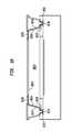
- FIG. 1is a sectional view of a packaged semiconductor chip 10 in accordance with an embodiment of the invention.
- the packaged chipis shown in an orientation in which a front face 102 of the semiconductor chip faces downwardly.
- the packaged chipincludes a semiconductor chip 100 having a front face 102 and a rear face 114 remote from the front face.
- the front face of the chip 100is covered by a lid or cover 104 which is assembled together with the semiconductor chip 100 to form the packaged chip 10 .
- the front face 102 of the semiconductor chip 100is oriented downwardly towards an upwardly facing inner surface 105 of the lid 104 .
- the semiconductor chip 100typically includes a semiconductor substrate in which one or a plurality of semiconductor devices 112 are disposed in a device region thereof below the front face 102 .
- the semiconductor chip 100also includes a plurality of dielectric layers overlying the substrate, in which conductive metal wiring layers and vias (not shown) are disposed.
- the semiconductor devices 112are disposed at the front face of the chip and/or between the front and rear faces of the chip.
- the package chipcan be referred to as a chip-scale package (“CSP”), because exterior lateral dimensions (e.g., in direction of arrow 102 ) of the packaged chip 10 are about the same as they would be for a bare chip.
- CSPchip-scale package
- the semiconductor chip 100typically is connected to the lid 104 through one or more standoff structures 124 , which may include an adhesive, an inorganic or organic material and/or a joining metal. Structures for supporting a lid at a constant spacing from a chip are described in the commonly owned U.S. Provisional Application No. 60/761,171 filed on Jan. 23, 2006, and U.S. Provisional Application No. 60/775,086 filed on Feb. 21, 2006, the disclosures of which are hereby incorporated herein by reference.
- the packaged chipmay include an interior cavity 106 between the front face 102 of the chip and the inner surface 105 of the lid 104 , as illustrated in FIG. 1 . Alternatively, the packaged chip 10 can be constructed without an interior cavity.
- the cavity's height 108 and the lateral dimensions, including lateral dimension 110are typically determined, as for example, by the height and dimensions of the structure 124 used to assemble the lid 104 with the semiconductor chip 100 .
- the lid 104consists essentially of a glass or polymeric material and is at least partially transparent to electromagnetic spectra at frequencies of interest.
- the lid 104may be only partially transparent to provide a filter function, or may be essentially transparent to a range of frequencies of interest.
- the semiconductor devices 112 in the semiconductor chip 100typically include electromagnetic transducer devices such as electromagnetic or electro-optic devices which either detect or output electromagnetic radiation.
- the semiconductor devicesmay be designed to emit or receive radio frequency and/or optical wavelengths of infrared, visible and/or ultraviolet or higher wavelength spectra including but not limited to x-ray wavelengths.
- the semiconductor devices 112can include acoustic transducer devices, such devices being designed to convert sound pressure waves received through a medium, e.g., air and/or other fluid medium (gas or liquid) to one or more electrical signals, or to convert one or more electrical signals into sound pressure waves.
- the packaged chipis a sensor unit in which the semiconductor devices 112 of the chip 100 include an imaging area 107 for capturing an image.
- Electronic circuits (not shown) in chip 100are connected to the semiconductor devices in the imaging area 107 for generating one or more electrical signals representing an image captured by the imaging area 107 .
- Numerous electrical circuitsare well known in the imaging art for this purpose.
- the semiconductor chip 100may be a generally conventional charge-coupled device (CCD) imaging chip with conventional circuits such as clocking and charge-to-voltage conversion circuits.
- CCDcharge-coupled device
- the semiconductor chipincludes a plurality of front contact pads 116 at the front face of the semiconductor chip. While not specifically shown in FIG. 1 , the semiconductor devices 112 in the device region are conductively connected to the front contact pads 116 . The semiconductor device, thus, are accessible conductively through wiring incorporated extending within or above one or more dielectric layers of the semiconductor chip 100 .
- the semiconductor chiphas surfaces 120 which are set at an angle away from the rear surface.
- surfaces 120may be sloped away from the rear face at angles other than right angles and the slope may either be gradual, e.g., having an angle of less than 45 degrees with respect to a normal to the rear surface, or the slope may be more abrupt, in which such angle is greater than 45 degrees relative to the normal.
- the surfaces 120may be at right angles to the rear face.
- the surfaces 120end at lowered rear surfaces 115 .
- the lowered rear surfaces 115face away from the front face 102 and are spaced therefrom by thinned regions 105 of the semiconductor chip 100 .
- Conductive vias 125extend between the front face 102 of the chip 100 and the lowered rear surfaces 115 .
- the conductive viasprovide conductive interconnection between the front contact pads 116 and conductive traces 126 overlying the lowered rear surfaces 115 and surfaces 120 .
- the conductive vias 125include a conductive layer overlying a dielectric layer 122 disposed within holes 127 extending between the front face and the lowered rear surfaces. Between the front face 102 and the lowered rear surface, the walls of the holes 127 can extend vertically, i.e., at right angles relative to the front face.
- the holes 127can be tapered in a direction from the lowered rear surface towards the front face such that the holes become smaller with increasing distance from the lowered rear surface.
- the holes 127can be tapered in a direction from the front face towards the lowered rear surface such that the holes become smaller with increasing depth from the front face.
- Each of the embodiments described belowcan include holes having any one of these available hole geometries.
- the conductive vias 125are in form of conductive traces extending extend upwardly from the contact pads 116 of the chip along walls of the holes 127 , the traces continuing upwardly along wall 120 and onto the rear face 114 .
- the conductive vias 125can be in form of holes 127 filled with conductive material, e.g., a metal.
- traces 126can extend from individual ones of the vias along a wall 120 and onto the rear face 114 .
- the dielectric layer 122preferably includes a conformally coated dielectric material. Preferably, there are no breaks in the conformal coating and the dielectric layer 122 provides good dielectric isolation with respect to the semiconductor chip 100 .
- the dielectric layer 122is a compliant layer, having sufficiently low modulus of elasticity and sufficient thickness such that the product of the modulus and the thickness provide compliancy. Specifically, such compliant layer can allow the contacts 128 and traces 126 attached thereto to flex somewhat. In that way, the bond between external conductive bumps 134 of the packaged chip 10 and terminals of a circuit panel (not shown) can better withstand thermal strain due to mismatch of the coefficient of thermal expansion (“CTE”) between the packaged chip 10 and a circuit panel (not shown).
- CTEcoefficient of thermal expansion
- the degree of compliancy provided by the product of the thickness of the dielectric layer 122 and its modulusare sufficient to compensate for strain applied to the conductive bumps due to thermal expansion mismatch between the chip 100 and the circuit panel.
- An underfill(not shown) can be provided between the exposed surface of the dielectric layer 130 and such circuit panel to enhance resistance to thermal strain due to CTE mismatch.
- the conductive traces 126conductively connect the conductive vias 125 to corresponding package contact pads 128 which overlie an exterior surface of the packaged chip 10 .
- the package contact pads 128overlie the rear face 114 of the semiconductor chip 100 .
- the conductive traces 126overlie the second dielectric layer 122 and extend over portions of the surfaces 120 and rear face 114 of the semiconductor chip.
- the conductive traces 126connect individual front contact pads 116 of the chip 100 with corresponding individual package contact pads 128 .
- Conductive bumps 134may be provided on the contact pads 128 .
- the thickness 160 of the microelectronic element 100 between the front and rear facestypically is less than 200 ⁇ m, and can be significantly smaller, for example, 130 nm, 70 nm or even smaller.
- the thickness 162 of the microelectronic element between the lowered surface 115 and the front face 102normally will be one half or less than one half of the thickness 160 .
- the thickness 162 of the microelectronic element at the lowered surfaceis significantly less than one half the thickness 160 . In one example, the thickness 162 is approximately 10 microns.
- a second dielectric layer 130overlies the conductive traces 126 and provides external isolation therefor.
- This layercan be referred to as an “external passivation layer” 130 of the package 10 .
- the second dielectric layercan include an inorganic or organic dielectric material or both.
- the second dielectricmay include an electrodeposited conformal coating or other dielectric material, for example, a photoimageable polymeric material, for example, a solder mask material. Photoimageable solder mask materials can be obtained from various manufacturers including Shipley and Toyo, among others.
- a metal structure 132 including a metal layer or stack of metal layers including a wettable metal layeroverlies the package contact pads 128 , and conductive bumps 134 overlie the metal structure 132 .
- the conductive bumps 134include a fusible metal having a relatively low melting temperature such as solder, tin, or a eutectic mixture including a plurality of metals.
- the bumps 134include a wettable metal, e.g., copper or other noble metal or non-noble metal having a melting temperature higher than that of solder or other fusible metal.
- Such wettable metalcan be joined with a corresponding feature, e.g., a fusible metal feature of an interconnect element such as a circuit panel to externally interconnect the packaged chip 10 to such interconnect element.
- the bumps 134include a conductive material interspersed in a medium, e.g., a conductive paste, e.g., metal-filled paste, solder-filled paste or isotropic conductive adhesive or anisotropic conductive adhesive.
- semiconductor chips 100preferably are packaged simultaneously by wafer-level processing, i.e., by processing performed simultaneously to a plurality of semiconductor chips 100 while they remain joined together as a portion of a waver or as an entire semiconductor device wafer 101 .
- wafer-level processingi.e., by processing performed simultaneously to a plurality of semiconductor chips 100 while they remain joined together as a portion of a waver or as an entire semiconductor device wafer 101 .
- the assembly of wafer with the attached lid 104is severed along dicing lane 12 and other dicing lanes not visible within the view of FIG. 2 into individual packaged semiconductor chips.
- FIG. 3Aa semiconductor device wafer or portion of a device wafer containing a plurality of chips 100 is mounted to a lid member 111 such that front faces 102 of the chips 100 having device regions 112 and front contacts 116 thereon, confront the lid member 111 .
- the lid member 111preferably has dimensions in lateral directions (directions extending in a plane defined by the inner surface 105 ) which are the same as those of the semiconductor device wafer 101 .
- Reference 12indicates a location of a dicing lane at a boundary between individual chips 100 .
- Dicing lanes 12 of the waferneed not be very wide.
- the locations of bond pads 116 of the chip 100need not be specially located, such that the bond pads usually are well away from the dicing lanes.
- a representative width of the dicing laneis approximately 40 ⁇ m (microns).
- a rear face 101 A of the device waferoverlies the front faces 102 of the chips. Desirably, at this stage of fabrication, the rear face 101 A is spaced uniformly from the front faces 102 of the chip by an initial thickness 272 of the device wafer.
- Locations of the bond pads 116 underlying the device wafer and dicing lane 12are indicated in a corresponding plan view ( FIG. 3B ) looking toward the rear face 101 A of the device wafer.
- a standoff structure 206supports the device wafer 101 at a distance 108 above the inner surface 105 of the lid member 111 .
- FIG. 3Cillustrates a preliminary stage of fabrication in which a plurality of standoff structures 206 can be formed extending outward from a major surface of the lid member 111 containing individual lid elements 104 attached together at dicing lanes 12 .
- each standoff structure 206typically has a rectangular shape aligned with vertically oriented dicing lanes 12 and aligned with horizontally oriented dicing lanes 14 which lie at the boundaries between individual lids to be severed from the original lid member 111 . As illustrated in FIG.
- the standoff structure 206has a form which can be described as that of a “picture frame ring shape.”
- the standoff structurecan include one or more inorganic dielectric materials, organic dielectric materials, semiconductors, conductors such as one or more metals, metallic compounds or a combination of such materials.
- the standoff structurecan be fabricated by additive processing or subtractive processing or both, as described in, for example, U.S. patent application Ser. No. 10/949,674 filed Sep. 24, 2004, or U.S. Provisional Application No. 60/761,171, the disclosures of which are hereby incorporated herein by reference.
- the standoff structureWhen the standoff structure includes a metal, it can be fabricated by a combination of steps including sputtering of a thin layer of metal followed by subtractive patterning and then electroplating the remaining structure with a final metal. Alternatively, the standoff structure can be formed by electroless plating, followed by subtractive patterning and electroplating. In a particular embodiment, the standoff structure 206 is fabricated by electrophoretic deposition of a polymer onto a preexisting sputtered or plated conductive layer, in a manner such as that described in the herein incorporated U.S. Provisional Application No. 60/775,086.
- the thickness of the device wafercan be reduced from the rear face 101 A. Grinding, lapping, or polishing from the rear face or a combination thereof can be used to reduce the thickness.
- the lid element 104 overlying the front face of the semiconductor chipassists in providing structural support to the semiconductor chip, increasing its rigidity to permit the thickness of the packaged chip to be reduced as desirable to a smaller thickness.
- the thickness of the device wafercan be reduced from about 700 nm to about 130 nm or less.
- the resulting device waferhas a reduced thickness 274 , as shown in FIG. 4 and the rear face 114 is separated from the front face 102 of each chip 100 by the thickness 274 .
- a recess 276is formed in the device wafer which extends downwardly from the rear face 114 towards the front face 102 of the device wafer.
- the recesscan be formed for example, by selectively etching the device wafer, after forming a mask layer where it is desired to preserve remaining portions of the rear faces 114 of the chips.
- a photoimageable layere.g., photoresist layer can be deposited and patterned to cover only portions of the rear face, after which a timed etch process can be conducted to form the recess 276 .
- the recesscan be formed as a stripe 278 extending in a linear direction 280 over the device wafer in alignment with the dicing lane 12 .
- elongated recesses 276desirably are formed simultaneously which extend in a vertical layout direction 280 of the device wafer in alignment with vertically extending dicing lanes.
- the vertically extending recesses 276can be formed to extend only along dicing lines of respective pairs of chips.
- the recessesmay not overlie corner portions of the chips 100 at intersections between the vertical dicing lanes 12 and horizontal dicing lanes 14 extending in a horizontal layout direction of the device wafer.
- horizontally extending recesses 284can be formed to overlie bond pads adjacent to the horizontal dicing lanes 14 of each chip. Both vertically extending recesses 276 and horizontally extending recesses 284 can be formed in the device wafer. In a particular example, recesses may be formed which overlie bond pads adjacent to only one of the dicing lanes which bound a chip.
- the recessescan be formed which overlie only two dicing lanes of the chip or which overlie only three dicing lanes or more dicing lanes which bound a chip.
- recessescan be made smaller than as shown in FIG. 6A , such that the recesses overlie only some bond pads of rows of bond pads which lie adjacent to the dicing lanes 12 of the device wafer 101 .
- recesses 286 aligned with dicing lanes 12can extend as stripes between respective edges 288 , 290 of the device wafer 101 .
- each recess 276desirably has a lowered surface 502 which is flat and equidistant from the front face 102 .
- Walls 504 of the recessextending downwardly from the rear face 114 towards the lowered surfaces, may be sloped, i.e., may extend at angles other a normal angle (right angle) to the rear surface 114 , as particularly illustrated in FIG. 5A .
- Wet etching processese.g., isotropic etching processes and sawing using a tapered blade, among others, can be used to form recesses having sloped walls 504 as illustrated in FIG. 5A .
- Laser dicing, mechanical milling, among otherscan also be used to form recesses having sloped walls.
- the wallsmay extend vertically downwardly from the rear face 114 at right angles to the rear face 114 .
- Anisotropic etching processes, laser dicing, laser drilling, mechanical removal processes, e.g., sawing, milling, ultrasonic machining, among others,can be used to form recesses having essentially vertical walls.
- a photoimageable layersuch as a photoresist is deposited onto the rear of the device wafer and patterned to form mask openings 506 overlying the lowered surface 502 in registration with bond pads 116 .
- an etch processis applied to the portions of the lowered surface 502 exposed within the mask openings so as to remove the semiconductor material underlying the mask openings.
- vias 708are formed which extend between the lowered surface in contact with the front contacts 116 .
- the etch processdesirably is conducted in a manner which selectively etches the semiconductor material, e.g., silicon, but preserves oxide material.
- the front contacts, e.g., bond pads 116 of a chipoverlie one or more layers of oxide material or other dielectric material which is used for passivation, as interlevel dielectric layers or other purpose of providing insulation or isolation on the chip.
- the semiconductor materialBy etching the semiconductor material in a selective manner which preserves the dielectric, over-etching can be performed as needed to etch through the thickness of the semiconductor material in all locations of the device wafer while maintaining a sufficient process window across the device wafer.
- the dielectric layer 710e.g., oxide layer, remains in place after forming the vias 708 .
- laser drilling or mechanical millingcan be used to form the vias 708 , in which case, surfaces of the front contact pads can be exposed within the vias.
- a dielectric layer 820is formed on walls 806 of the vias, walls 504 and the rear surfaces 114 of chips.
- Various methodscan be used to form such dielectric layer.
- a flowable dielectric materialis applied to the rear surface 114 of a wafer 101 containing chips 100 and the flowable material is then more evenly distributed across the rear surface of the wafer during a “spin-coating” operation, followed by a drying cycle which may include heating.
- a thermoplastic film of dielectric materialcan be applied to the rear surface of the device wafer 101 after which the assembly including the wafer and lid element is heated, causing the film to flow downward onto the lowered surfaces 115 and into the vias 708 .
- vapor depositioncan be used to form the dielectric layer.
- the assembly including the device wafer with the lid element attached theretois immersed in a dielectric deposition bath to form a conformal dielectric coating or layer 820 .
- a dielectric deposition bathPreferably, an electrophoretic deposition technique is utilized to form the conformal dielectric coating, such that the conformal dielectric coating is only deposited onto exposed conductive and semiconductive surfaces of the assembly.
- the semiconductor device waferis held at a desired electric potential and an electrode is immersed into the bath to hold the bath at a different desired potential.
- Electrophoretic depositionoccurs so long as a sufficiently strong electric field is maintained between the surface to be coated thereby and the bath.
- the electrophoretically deposited coatingis self-limiting in that after it reaches a certain thickness governed by parameters, e.g., voltage, concentration, etc. of its deposition, deposition stops.
- Electrophoretic depositionforms a continuous and uniformly thick conformal coating on conductive and/or semiconductive exterior surfaces of the assembly.
- the electrophoretically deposited coatingpreferably does not form on the remaining dielectric layer 710 overlying the contacts 116 , due to its dielectric (nonconductive) property.
- a property of electrophoretic depositionis that is does not form on a layer of dielectric material overlying a conductor provided that the layer of dielectric material has sufficient thickness, given its dielectric properties.
- electrophoretic depositionwill not occur on dielectric layers having thicknesses greater than about 10 microns to a few tens of microns.
- the conformal dielectric layer 820is formed from a cathodic epoxy deposition precursor.
- a polyurethane or acrylic deposition precursorcould be used.
- electrophoretic coating precursor compositions and sources of supplyare listed in Table 1 below.
- FIG. 8Billustrates that the vias 710 above the bond pads remain open after the electrophoretic deposition. After electrophoretically depositing the conformal dielectric coating, processing is then begun for forming conductive traces which connect the front contact pads of the semiconductor chips to exterior contacts of the packaged chips.
- the substrateis now prepared for processing which will form conductive traces 126 and lands 128 .
- laser drilling, mechanical milling or other appropriate techniquescan be used at this stage to open the bottoms of the vias adjacent to the front contact pads.
- any part of a preexisting dielectric layer 710 ( FIG. 8A ) of the chipremains in alignment with the contacts 116 , such layer can be removed in this step.
- Such removalcan be accomplished, for example, laser drilling, mechanical milling, or other suitable technique.
- Other possible removal techniquesinclude various selective etching techniques which can be isotropic or anisotropic in nature.
- Anisotropic etch processesinclude reactive ion etch processes in which a stream of ions are directed towards surfaces to be etched. Reactive ion etch processes are generally less selective than isotropic etch processes such that surfaces at which ions strike at high angles of incidence are etched to a greater extent than surfaces which are oriented with the stream of ions.
- a mask layeris desirably deposited to overlie the conformal dielectric coating 820 and openings are formed therein which are aligned with the vias 708 . In such way, the etch process avoids removing portions of the dielectric coating 820 other than that which lies within the vias 708 .
- the conductive traces 126 and lands 128are now formed to overlie the conformal dielectric coating 820 .
- An exemplary method of forming the traces and landsinvolves depositing a metal layer to overlie the conformal dielectric coating 220 .
- the depositioncan be conducted while portions of those surfaces are protected by a masking layer.
- the metal layerpreferably is deposited by sputtering a primary metal layer onto exposed surfaces of the assembly, or by electroless deposition. This step can be performed by blanket deposition onto the rear face, walls and lowered surface of the device wafer, for example.
- the primary metal layerincludes or consists essentially of aluminum.
- the primary metal layerincludes or consists essentially of copper.
- the primary metal layerincludes or consists essentially of titanium.
- One or more other exemplary metalscan be used in a process to form the primary metal layer.
- a photoimageable layerthen is deposited to overlie the primary metal layer and a three-dimensional photolithographic patterning process is utilized to pattern the primary metal layer, such as the process described in U.S. Pat. No. 5,716,759 to Badehi, the disclosure of which is hereby incorporated by reference herein. Thereafter, remaining portions of the photoimageable layer are removed. As a result, individual conductive patterns are formed which correspond to the dimensions of conductive traces to be formed thereon.
- the photoimageable layeris removed from the device wafer and an electroplating process is used to plate a secondary metal layer onto the primary metal layer to form individual conductive traces 126 extending from the front contact pads 116 along the walls 120 and onto the rear faces 114 of the semiconductor chips.
- the secondary metalmay include nickel or other noble metal.
- the electroplated second metal on the primary metal layercompletes the conductive traces.
- an optional third metal layersuch as gold, platinum or palladium may be plated onto the secondary metal for providing corrosion resistance to complete the conductive traces.
- an additional dielectric layer 230is deposited to overlie each of the conductive traces 226 extending along the rear surface 114 and walls 120 .
- the additional dielectric layer 230is deposited by an electrophoretic deposition process such as described above with reference to FIGS. 8A-B .
- a patterned mask layer including a photoresist, oxide mask, etc.is formed on the contacts 128 .
- the resulting dielectric layer 230is avoided from being formed on contacts 128 by the patterned mask layer.
- the patterned mask layerthen is removed to expose the contacts 128 within openings in the dielectric layer 230 .
- the dielectric layer 230can be formed by spin-coating or spray coating a photoimageable dielectric such as an encapsulant or a solder mask material towards the rear face 114 and walls 120 of the device wafer to form a relatively uniformly thick coating. Thereafter, openings can be formed in the conformal dielectric layer 230 in registration with the contacts 128 by photolithographic process. One or more processes, e.g., heating etc. may be performed to cause the dielectric layer 230 to harden after the initial deposition of the photoimageable material.
- a photoimageable dielectricsuch as an encapsulant or a solder mask material
- a wettable metal layer 132e.g., an “under bump metallization” or (“UBM”) is formed within the openings in the dielectric layer 230 , the wettable layer being in contact with each of the contacts 128 .
- a diffusion barrier layere.g., a conductive layer including titanium, tungsten, tantalum, or other similar metal is formed in contact with the contacts 128 .
- a layer including a first wettable metalcan be deposited to overlie the barrier layer, such layer including a metal such as nickel, copper or other metal which desirably includes a noble metal.
- a layer of goldcan be deposited as a final layer of wettable metal.
- conductive bumps 134can be formed in contact with the wettable metal layer over each contact.
- Conductive bumpscan be formed which include a fusible metal such as a solder, tin or eutectic composition, or which include a conductive paste, e.g., solder-filled or silver-filled paste, among others.
- the conductive bumpscan include one or more conductive materials.
- the conductive bumpscan include one or more noble metals, for example, copper, nickel, etc.
- the conductive bumpsmay be formed by placing spheres including a fusible metal such as solder, tin or eutectic onto the wettable metal layer 232 and then heating the conductive bumps thereto to fuse them to the wettable metal layer 232 .
- a fusible metalsuch as solder, tin or eutectic
- the packaged chipsare severed from each other along dicing lane 12 by sawing or other dicing method to form individual packaged chips 10 as illustrated in FIGS. 10A-10B .
- a variety of exemplary processes for severing packaged chips into individual unitsare described in the herein incorporated commonly owned U.S. Provisional Application Nos. 60/761,171 and 60/775,086, any of which can be used to sever the packaged chips to form individual packaged chips as shown in FIGS. 10A-10B .
- a camera module 1030includes a sensor unit 1020 having contacts 1042 disposed on the rear face of the sensor unit, i.e., on the surface of the semiconductor chip 1000 opposite from the front surface 1028 which carries the imaging area 1026 .
- the sensor unitcan be such as that shown and described above with reference to FIG. 1 .
- Similar sensor units and camera modulesare described in commonly owned U.S. patent application Ser. No. 11/265,727 filed Nov. 2, 2005 and Ser. No. 11/322,617 filed Dec. 30, 2005, the disclosures of which are hereby incorporated herein by reference.
- the contacts 1042 of the sensor unitare connected to terminals 1080 of a circuit panel 1070 by masses 1082 of fusible conductive material such as solder.
- the optical unit 1050 in this arrangementincludes a turret or support structure 1051 having a mounting portion 1052 arranged to hold one or more lenses or other optical elements 1058 .
- the support structure 1051also includes a plurality of rear elements 1062 in the form of elongated posts 1062 projecting rearward from the mounting portion 1052 . These posts have rear surfaces 1054 which abut or mechanically engage a reference plane in the sensor unit to position the optical unit relative to the sensor unit. In the example illustrated in FIG. 11 , the rear surfaces 1054 abut the front surface of the transparent cover 1034 which overlies the imaging area 1026 .
- the turret or support structureincludes registration features, e.g., posts, pins, recesses, or the like, for mechanically setting the height of the optical unit 1050 with respect to the chip 1000 , while limiting tilt of the turret with respect to the imaging area 1026 of the chip.
- connection between the rear surfaces of the posts 1062 and the front surface 1034level and uniform in thickness.
- metallic attachment features or pads 1055can be provided at the outer surface 1036 of the cover 1034 , which are metallurgically bonded, e.g., via diffusion bonding, to metallic features at the rear surfaces 1054 of the posts 1062 .
- a somewhat thin adhesivecan be used to bond the rear surfaces of the posts to the cover.
- the turret or support structure 1051in place of posts, includes a rear element which encloses or substantially encloses a volume having a cylindrical or polyhedral shape.
- a rear elementcan be provided which has a cylindrical wall or polyhedral shaped (e.g., box-shaped) wall, in which the rear surface of the rear element abuts against a reference plane of the sensor unit such as provided at the outer surface 1036 of the cover 1034 .
- sensor unit 1020is mounted with the front of the sensor unit, and hence, imaging area 1028 facing forwardly, toward the rear or bottom surface of circuit panel 1070 .
- the contacts 1042 of the sensor unitare connected by suitable leads or wire bonds 1002 to the conductors 1076 of the circuit panel.
- the rear elements 1062 of the optical unit 1050project through a hole 1072 in the circuit panel aligned with the imaging area 1028 .
- hole 1072is large enough to accommodate the light path from the optical element to the imaging area and also accommodate the rear elements 1062 .
- a similar arrangementcan be used with sensor units having contacts on the front face, as discussed above.
- a camera module in accordance with a further embodiment of the inventionincludes a sensor unit 920 , depicted in broken lines, disposed on the bottom or rear side of a circuit panel 970 .
- the imaging area of the chip in the sensor unitis aligned with a hole 972 in the circuit panel.
- the optical unit 950 in this arrangementincludes a turret or support structure 952 having a mounting portion 902 arranged to hold one or more lenses or other optical elements 958 .
- the support structure 952also includes a plurality of rear elements 962 in the form of elongated posts projecting rearward from the mounting portion 902 .
- postsextend through apertures 974 in the circuit panel, and thus mechanically engage the sensor unit to position the optical unit relative to the sensor unit as discussed above.
- postsdefine gaps between them as, for example, gap 963 a between posts 962 a and 962 b .
- the circuit panel 970may extend into the gaps, and hence may extend between the sensor unit and optical unit, which facilitates making connections to the sensor unit as discussed above.
- the gapshave substantial height.
- the height H G of the gap in the completed assemblyis equal to the height of the mounting element 902 above the front surface 901 of circuit panel 970 .
- the height H Gdesirably is on the order of 2 mm or more, more desirably 5 mm or more, and most preferably 1 cm or more.
- the width of each gap(i.e., the horizontal distance, parallel to the circuit panel, between rear elements 962 a and 962 b ) desirably also is at least about 2 mm, more desirably at least about 5 mm, and most desirably at least about 1 cm.
- provision of such large gapsallows access into the area between the optical element and hole 972 for performing operations on the completed assembly.
- the large gapscan be provided without increasing the overall height of the assembly.
- the distance between the optical elements such as lens 958 and the sensor unitis set by the optical properties of the system as, for example, the focal length of lens 958 . Therefore, the lens must be supported at a substantial distance forward of the circuit panel in any event.
- a module or assembly in accordance with the embodiment of FIG. 13can be treated after assembly by performing operations on the sensor unit through the gap or gaps, and desirably also through hole 972 in the circuit panel.
- the assemblymay be subjected to a cleaning operation in which a cleaning fluid, a cleaning implement, or both are inserted into one or more of the gaps and through hole 972 to clean the surface of the sensor module.
- the sensor moduleincorporates a cover facing forwardly toward the rear or bottom surface of the circuit panel, the area of the cover aligned with the hole which includes the area aligned with the imaging area of the sensor chip can be cleaned. The ability to perform such a cleaning operation on the completed assembly counteracts the effects of contamination during the assembly process.
- the sensor unitmay not incorporate a separate cover, but instead may consist only of a “bare” semiconductor chip having an imaging area and having a passivation layer in the form of a thin coating effective to protect the elements of the bare chip from chemical or mechanical damage during the assembly process.
- a bare imaging chiptypically requires very stringent precautions during handling to avoid deposition of dirt overlying one or more imaging elements. The requirements are somewhat less stringent for sensor units which incorporate a cover. However, by post-cleaning after assembly, the less stringent requirements may be applied to assembly of sensor units which do not include a cover.
- the sensor unitmay include a sacrificial layer overlying the front of the sensor unit as, for example, a sacrificial layer overlying the outer surface of the cover in a sensor unit which includes a cover, or a sacrificial layer overlying the imaging area of the chip in a sensor unit which does not include a cover.
- the assemblyis fabricated with the sacrificial layer in place.
- the completed assemblyis then subjected to an operation in which the sacrificial layer, or at least that portion of the sacrificial layer aligned with the imaging area of the sensor unit, is removed through hole 972 and through the one or more of the gaps 963 in the support structure 952 .
- the sacrificial layermay be removed by dissolving it, or by mechanically engaging it and peeling it away from the sensor unit. Removal of the sacrificial layer removes any contaminants which may have accumulated on that layer.
- a toolmay be inserted into the gap or gaps to engage the conductors of the circuit panel and bond them to the contacts of the sensor unit.
- a wire-bonding toolmay be used to provide wire bonds extending between the conductors and the sensor unit through hole 972 , or through one or more of the additional apertures 974 , or through other apertures (not shown) provided in the circuit panel for this purpose.
- the rear elementsmay be in the form of plates or ribs. Also, it is not essential to provide multiple gaps; only one gap may be sufficient for some operations.
- FIG. 14illustrates an optical unit or camera module in accordance with another embodiment of the invention.
- a sensor unit 1120has contacts 1142 conductively connected to terminals 1144 of a circuit panel which overlies the outer surface 1138 of the cover 1128 , e.g., via solder masses 1146 .
- Walls 1130 of the coverare preferably sloped such that the radii at edges 1132 of the walls are gradual and preferably provide a smooth transition between a set of first contacts 1134 provided on the front surface 1102 of the chip and the walls 1130 .
- a set of conductive traces 1156extend from the first contacts 1134 along walls 1130 and onto the outer surface 1138 of cover 1128 , these being conductively connected to contacts 1142 .
- a dielectric coating 1158such as an epoxy or other polymeric material deposited preferably via electrophoretic deposition, overlies the conductive traces 1156 and is utilized as a passivation layer, e.g., solder mask with openings exposed above the contacts 1142 .
- an optical unit 1150has a set of rear elements 1162 which extend rearward from a structure supporting an optical element 1158 , e.g., a lens or other optical device selected from, among others, refractive or diffractive elements, filters, reflectors and scatterers.
- an optical element 1158e.g., a lens or other optical device selected from, among others, refractive or diffractive elements, filters, reflectors and scatterers.
- rear surfaces 1164 of the rear elementare adapted to extend through a hole 1172 in the circuit panel to abut or engage the outer surface 1138 of the cover 1128 or other reference plane of the sensor unit 1120 .
- the circuit panelhas a hole extending through the panel in alignment with the imaging area of the sensor unit. Such a hole forms a transparent region in the circuit panel.
- the circuit panelincludes a solid but transparent region in alignment with the imaging area of the sensor unit.
- the circuit panelmay be formed from a transparent dielectric material, in which case the transparent region of the circuit panel may be provided simply by routing the conductors of the circuit panel so that no conductors cross the transparent region.
- FIG. 15is a sectional view illustrating a packaged chip 1500 in accordance with a variation of the packaged chip 10 ( FIG. 1 ).
- the external contacts 1528 of the chipare exposed at ledges 1515 of the chip defined by the lowered surfaces of the chip, the external contacts 1528 being disposed adjacent to edges 1502 of the semiconductor chip.
- Interconnection to external elementsuch as a circuit panel can be made by forming bond wires 1530 connected to the external contacts 1528 at first ends and to terminals 1532 of a circuit panel 1540 at second ends, the circuit panel having an opening 1542 in registration with the optoelectronic element 1512 , e.g., image sensor, of the chip.
- conductive massese.g., solder masses, solder balls, etc., can be used to interconnect the contacts 1528 to an external element disposed above the rear surface 114 of the chip.
- FIG. 16Ais a sectional view illustrating a packaged chip 1600 in accordance with a variation of the packaged chip 10 ( FIG. 1 ).
- large openings 1604 in the chip 1602extend through much of the thickness 1606 of the chip, and vias 1608 extend from within the large openings to the front conductive contacts 116 .
- the large openings 1604can be provided in form of holes overlying individual ones of the vias 1608 , or alternatively, in form of channels extending over a row or rows of bond pads of each individual chip as shown in FIG. 6A , or in form of channels which extend the length of a wafer which includes the chips ( FIG. 6B ).
- the thickness of the chip 1606 while it is in wafer formis reduced from its original thickness prior to performing steps to form the packaged chips shown in FIG. 16A .
- a device wafer containing the chipcan be thinned by grinding or lapping from the rear surface such that it has a thickness of about 200 microns before bonding the device wafer to a corresponding lid element. If the grinding is performed after bonding the wafer to the lid element, the thickness can be reduced even more, such as to a thickness of 50 microns, for example.
- conductive traces 1610extend upwardly from bond pads 116 of the chip along walls of the vias 1608 and openings 1604 .
- vias 1608can be filled with conductive material.
- traces 1610can extend from individual ones of the vias upwardly along a wall of an opening 1604 shared by several vias (See plan view ( FIG. 16B ) looking toward rear face). Traces 1610 are connected to external contacts 1628 at locations overlying the rear surface 1614 of the chip 1602 .
- FIGS. 1 and 15 through 24 Bshow embodiments having either filled small vias 1908 (e.g., FIG. 19A ) or traces extending along the vias (e.g., vias 1608 ), the alternative structures of the conductive vias are interchangeable in each case.
- the via 1608 and the large opening 1604can be filled with a conductive material overlying a dielectric layer 1620 disposed on walls of the via 1608 and opening 1604 .
- FIG. 17illustrates a packaged chip according to a variation of the embodiment shown and described above with reference to FIG. 15 .
- This examplevaries from that shown in FIG. 15 in that the optically transmissive lid, rather than the chip, has ledges 1715 defined by lowered surfaces adjacent to its edges and contacts 1728 disposed on the ledges.
- FIG. 17illustrates an embodiment in which one or more dielectric layers 1720 , 1722 , e.g., a spin-coated dielectric, solder mask, etc., may extend over a top surface of the lid.
- the lid 1704typically has dielectric properties, such dielectric layer may not be necessary and can usually be omitted.
- FIG. 17illustrates a packaged chip according to a variation of the embodiment shown and described above with reference to FIG. 15 .
- the optically transmissive lidrather than the chip, has ledges 1715 defined by lowered surfaces adjacent to its edges and contacts 1728 disposed on the ledges.
- FIG. 17illustrates an embodiment in which one
- an inner surface 1706 of the lidis spaced from the front surface 1702 of the chip by a support structure 1710 .
- the viasdesirably are formed after a lid wafer containing the lid is joined to a device wafer containing the chip 1700 , with the support structure 1710 between the device wafer and the lid wafer.
- Various etching, milling, laser or mechanical drilling processessuch as described above can be used to form holes 1714 in the lid and the support structure 1710 to expose the contacts 1716 after which the vias are metallized and the contacts 1728 , traces, etc., are formed.
- FIG. 18illustrates a packaged chip according to a variation of the embodiment shown in FIG. 17 , which also has similarities with the embodiment shown in FIGS. 16A-B .
- traces 1824 extending along walls of the large openings 1804 in the lidare connected at first ends to metallized vias 1808 and at second ends to external contacts 1828 overlying the top surface 1844 of the lid 1820 .
- the viasextend through the support structure 1810 to the conductive contacts 1816 of the chip.
- Electrical interconnection to an external elementcan be provided through bond wires attached to the external contacts 1828 or by way of solder masses, e.g., solder balls, bumps, etc.
- FIG. 19Ais a sectional view illustrating a stackable chip-scale packaged chip 1910 in accordance with another embodiment of the invention.
- the packaged chipmay include a particular type of microelectronic device, such as a dynamic random access memory (“DRAM”).
- DRAMdynamic random access memory
- the packaged chip 1910has similar features to the packaged chip 1600 ( FIG. 16A ) described above, in that conductive vias 1908 extending inwardly from the front face 1902 of the chip 1901 connect to traces 1924 extending along walls of a large opening in the rear face 1914 of the chip.
- the packaged chip 1900does not include a lid overlying the front face, and the conductive vias 1908 are connected to bond pads 1909 by way of redistribution traces 1912 extending along the front face of the chip 1901 .
- FIG. 16Athe packaged chip 1900 has similar features to the packaged chip 1600 ( FIG. 16A ) described above, in that conductive vias 1908 extending inwardly from the front face 1902 of the chip 1901 connect to traces
- FIG. 19Bis a corresponding plan view looking towards a rear face 1914 of the packaged chip.
- the view in FIG. 19Ais taken along line 19 A- 19 A′ of FIG. 19B .
- traces 1924extend from vias 1908 upwardly along walls 1926 of the large opening 1904 and onto rear surface 1914 .
- the traces 1924connect to external contacts 1928 which overlie the rear face 1914 of the chip.
- FIG. 19Ca plan view is provided looking towards the front face of the chip 1901 , the chip including a DRAM, for example.
- bond pads 1909are typically provided in rows between memory circuits 1920 .
- FIG. 19Ais a view taken through line 19 A- 19 A′ of FIG. 19C .
- Redistribution traces 1912 on the front face 1902connect the bond pads 1909 to the conductive vias 1908 .
- the tracescan be arranged as shown in FIGS. 19B , 19 C such that some traces extend in a first direction away from the conductive vias and other traces extend in a second direction away from the vias, where the second direction is opposite the first direction. In this way, bond pads to the left side of the conductive vias are connected to some conductive vias and bond pads to the right side of the conductive vias are connected to other conductive vias.
- the conductive vias 1908are tapered such that they become smaller in a direction from the front face 1902 towards the rear face 1914 of the chip.
- the conductive viasare insulated from the semiconductor material of the chip by a dielectric layer 1922 .
- a passivation layer 1924overlies the front face 1902 of the chip including the conductive vias 1908 . Openings 1934 in the dielectric layer expose contacts 1936 at the front face of the chip. Desirably, the front face contacts 1936 are not in registration with the bond pads 1909 , although they can be.
- a dielectric fill material 1940desirably overlies the traces 1924 within the large opening 1904 for providing electrical isolation between traces as well as mechanical support to the packaged chip 1901 .
- a dielectric layer 1942e.g., a solder mask, overlies the traces 1924 . Openings 1944 in the dielectric layer expose rear face contacts 1946 of the chip.
- front face contacts 1936 and rear face contacts 1946By providing both front face contacts 1936 and rear face contacts 1946 , several packaged chips can be stacked one on top of the other to form a stacked assembly 1950 of packaged chips ( FIG. 19D ).
- the front face contactsare aligned with the rear face contacts. Connection between respective adjacent ones of the packaged chips in the stacked assembly is through conductive masses.
- the dielectric layer 1930 on the front face and the dielectric layer 1942 on the rear faceprovide electrical isolation between adjacent packaged chips 1910 in the assembly except where interconnection is provided.
- An advantage of the stacked assembly 1950is that the front face and rear face contacts are offset from the large openings 1904 in the packaged chip. Therefore, pressure exerted upon the stacked assembly when interconnecting the packaged chips is felt primarily at those contacts at locations away from the large openings. Such arrangement helps to avoid applying pressure to the packaged chip at the large opening where the semiconductor chip may possibly be weakened by the removal of semiconductor material to form the large opening.
- One potential benefit of having offset contactsis the ability to provide redistribution traces between the actual bond pads of the chip and the front and rear face contacts.
- Chip select features of certain types of memoriese.g., DRAMs, may require that certain bond pads of chips not be connected to the bond pads of other chips which directly overlie them.
- FIG. 19Eis a sectional view illustrating a variation of the embodiment illustrated in FIGS. 19A-19C .
- rear face contacts 1946 ′are exposed at the rear face at both a left side and a right side of the large opening 1904 .
- front face contacts 1936 ′are exposed at the front face at both a left side and a right side of the opening 1904 .
- Traces 1926 ′connect the two rear face contacts 1946 ′ to the same conductive via 1908 .
- FIG. 19Fis a sectional view illustrating a corresponding stacked assembly in which conductive masses 1952 ′ join the front face contacts on respective left and right sides of the large opening to the rear face contacts on respective left and right sides of the large opening.
- Another possible benefit of the arrangement shown in FIGS. 19E-Fis reduced inductance between packaged chips, because current flowing between adjacent chips now flows through a set of both left and right contacts per each signal.
- FIG. 20Ais a sectional view illustrating an advantage of the stackable packaged chip 1910 when the chip includes a DRAM.
- Certain types of semiconductor chips including DRAMSinclude capacitors formed in high aspect ratio trenches 1960 that extend downwardly from the front face of the chip. Often, the bond pads of the chip are disposed in close proximity to an array 1962 of such trench capacitors.
- interconnection between the front face contacts and the rear face contactsis through a large opening which is at some distance from the trench capacitor arrays 1962 .
- interconnection between adjacent chips 1910 in the stackcan be provided using interconnects extending through the chip which do not interfere with the placement or function of the trench capacitor arrays.
- FIG. 21Aillustrates one example interconnection.
- a conductive via 2108formed to extend downwardly from the front face 2102 of the chip is filled with a metal.
- a metalFor example, after etching a hole from the front surface, a relatively thin layer of metal can be sputtered to cover the walls and bottom of the hole. Thereafter, electroplating can be used to form the metal filling.
- the large opening 2104is formed by chemical etching, for example, which selectively etches the semiconductor material while preserving the metal of which the conductive via is formed.
- a result of over-etching the opening 2104is to fully expose a top surface 2170 of the conductive via.
- the dielectric layer 2122is formed and then an opening is made in the dielectric layer overlying the via 2108 , such as by use of a laser.
- the lasercan selectively remove the dielectric layer from over the top surface of the via because it is in a different focal plane from that of the dielectric layer which overlies the bottom 2106 of the large opening.
- the conductive trace 2124is formed, the trace contacts the entire top surface 2170 of the via 2108 .
- FIG. 22Aillustrates another example interconnection.
- the large opening 2204is formed by sawing after forming the conductive via.
- an openingis made in the dielectric layer, such as through use of a laser.
- the laser openingis restricted in size in order to avoid forming openings where the dielectric layer contacts the semiconductor material in the bottom of the opening 2206 .
- FIGS. 23A through 23Fare sectional views illustrating various alternatives for filling the large openings of the chip after forming conductive traces therein.
- a flowable dielectric fill material 2330is deposited or dispensed into the large opening or onto a rear face of the chip.
- the flowable dielectric materialis caused to be distributed into the opening, e.g., as by spin-coating or heat treatment such that the fill material fills the opening 2304 and provides a surface approximately even with the rear face 2314 .
- a solder mask 2332then is deposited to overlie the fill 2330 and the trace 2328 , an opening in the solder mask exposing a rear face contact 2346 .
- FIG. 23Billustrates an alternative in which the fill material 2340 has greater volume than the large opening, such that the fill 2340 protrudes above the rear face 2304 .
- the fillmay protrude above the rear face 2314 .
- FIG. 23Cillustrates another example when the volume of the fill 2350 is less than the volume of the opening 2304 or when the fill 2350 is not evenly distributed.
- FIG. 23Dillustrates another alternative similar to that shown in FIG. 23A , but in which the solder mask layer 2372 is deposited prior to depositing the fill material 2370 .
- FIG. 23Eillustrates an example similar to that shown in FIG. 23B , but in which the solder mask layer 2382 is deposited prior to depositing the fill material 2380 .
- FIG. 23Fillustrates an example similar to that shown in FIG. 23C , but in which the solder mask layer 2392 is deposited prior to depositing the fill material 2390 .
- FIG. 24Ais a sectional view illustrating a variation of the packaged chip illustrated in FIGS. 19A through 19C .
- FIG. 24Bis a magnified view showing the conductive via 2408 thereof.
- the conductive via 2408is formed from processes applied through the large opening in a direction towards the front face 2402 of the chip. In this case, processing is similar to that described above with reference to FIGS. 16A-B above.
- the device wafer including the chip 2400can be temporarily mounted front face down onto a carrier wafer (not shown) after forming front face contacts 2436 , traces 2432 and dielectric layer 2422 on the front face.
- holescan be formed for the vias from within the large opening, such as by laser drilling, etching, mechanical milling, etc.
- the carrier wafercan provide mechanical support to the conductive trace 2402 to help keep it in place at the bottom of the hole.
- the via and the large openingcan be metallized by simultaneous processing to form the conductive trace 2442 extending within the via, the large opening and onto the rear face 2414 .
- FIG. 25Aillustrates a chip 2510 having exposed chip-to-chip interconnects in form of solder balls 2550 .
- a solder ball 2550is joined to a top surface of the conductive via 2508 within the large opening 2504 .
- the conductive viamay be conductively connected to a bond pad 2509 or other contact on the front face 2502 of the chip 2510 , such as by way of a conductive trace.
- a passivation layer 2522overlies the conductive trace 2512 and bond pad 2509 , the passivation layer 2522 having an opening in registration with the conductive via 2508 .
- FIG. 25Billustrates a stacked assembly including a plurality of the chips 2510 illustrated in FIG. 25A , each chip being interconnected to the next adjacent chip by way of the solder ball 2550 between them.
- FIG. 26Aillustrates a variation of the embodiment shown in FIG. 25A in which a solder ball 2650 is joined to a bottom surface 2528 of the conductive via 2608 such that it protrudes downwardly below the front face 2602 of the chip.
- FIG. 26Billustrates a stacked assembly including a plurality of the chips 2610 as conductively joined together by way of the solder balls 2650 between adjacent chips 2610 .
- FIG. 27Aillustrates another variation of the embodiment shown in FIG. 25A in which a stud bump 2750 , e.g., consisting essentially of gold or other metal, is joined to the top surface 2718 of the conductive via 2708 .
- FIG. 27Billustrates a corresponding stacked assembly, wherein the stud bumps 2750 conductively interconnect adjacent ones of the chips.
- FIG. 28Aillustrates yet another variation, similar to that shown in FIG. 26A , in which the stud bump is joined to a bottom surface of the conductive via such that the stud bump protrudes downwardly from the front face 2802 of the chip.
- FIG. 28Billustrates a corresponding stacked assembly in which chips 2810 as shown in FIG. 28A are conductively interconnected by the stud bumps 2850 .
- conductive tracesextend from conductive features at the front face of a semiconductor chip along edges of a lid or along walls of openings formed in a lid covering the semiconductor chip and onto an outer surface of the cover element.
Landscapes
- Engineering & Computer Science (AREA)
- Microelectronics & Electronic Packaging (AREA)
- Computer Hardware Design (AREA)
- Power Engineering (AREA)
- Physics & Mathematics (AREA)
- Condensed Matter Physics & Semiconductors (AREA)
- General Physics & Mathematics (AREA)
- Multimedia (AREA)
- Signal Processing (AREA)
- Internal Circuitry In Semiconductor Integrated Circuit Devices (AREA)
- Solid State Image Pick-Up Elements (AREA)
- Semiconductor Memories (AREA)
Abstract
Description
| TABLE 1 | |||
| ECOAT NAME | POWERCRON 645 | POWERCRON 648 | CATHOGUARD 325 |
| MANUFACTURERS |
| MFG | PPG | PPG | BASF |
| TYPE | CATHODIC | CATHODIC | CATHODIC |
| POLYMER BASE | EPOXY | EPOXY | EPOXY |
| LOCATION | Pittsburgh, PA | Pittsburgh, PA | Southfield, MI |
| APPLICATION DATA |
| Pb/Pf-free | Pb-free | Pb or Pf-free | Pb-free |
| HAPs, g/L | 60-84 | COMPLIANT | |
| VOC, g/L (MINUS WATER) | 60-84 | <95 | |
| CURE | 20 min/175 C. | 20 min/175 C. |
| FILM PROPERTIES |
| COLOR | Black | Black | Black |
| THICKNESS, μm | 10-35 | 10-38 | 13-36 |
| PENCIL HARDNESS | 2H+ | 4H |
| BATH CHARACTERISTICS |
| SOLIDS, % wt. | 20 (18-22) | 20 (19-21) | 17.0-21.0 |
| pH (25 C.) | 5.9 (5.8-6.2) | 5.8 (5.6-5.9) | 5.4-6.0 |
| CONDUCTIVITY (25 C.) μS | 1000-1500 | 1200-1500 | 1000-1700 |
| P/B RATIO | 0.12-0.14 | 0.12-0.16 | 0.15-0.20 |
| OPERATION TEMP., C. | 30-34 | 34 | 29-35 |
| TIME, sec | 120-180 | 60-180 | 120+ |
| ANODE | SS316 | SS316 | SS316 |
| VOLTS | 200-400 | >100 | |
| Pb/Pf-free | Pb-free | Pb-free | |
| HAPs, g/L | |||
| VOC, g/L (MINUS WATER) | |||
| CURE | 20 min/149 C. | 20 min/175 C. | 20 min/175 C. |
| FILM PROPERTIES |
| COLOR | Clear (+dyed) | Black | Black |
| THICKNESS, μm | 10-35 | 10-35 | |
| PENCIL HARDNESS | 4H |
| BATH CHARACTERISTICS |
| SOLIDS, % wt. | 7.0 (6.5-8.0) | 10-12 | 9-11 |
| pH (25 C.) | 5.5-5.9 | 7-9 | 4.3 |
| CONDUCTIVITY (25 C.) μS | 450-600 | 500-800 | 400-800 |
| P/B RATIO | |||
| OPERATION TEMP., C. | 27-32 | 23-28 | 23-28 |
| TIME, sec | 60-120 | ||
| ANODE | SS316 | 316SS | 316SS |
| VOLTS | 40, max | 50-150 | |
Claims (18)
Priority Applications (1)
| Application Number | Priority Date | Filing Date | Title |
|---|---|---|---|
| US13/672,067US8735205B2 (en) | 2007-03-05 | 2012-11-08 | Chips having rear contacts connected by through vias to front contacts |
Applications Claiming Priority (4)
| Application Number | Priority Date | Filing Date | Title |
|---|---|---|---|
| US90509607P | 2007-03-05 | 2007-03-05 | |
| US12/072,508US8405196B2 (en) | 2007-03-05 | 2008-02-26 | Chips having rear contacts connected by through vias to front contacts |
| US12/784,841US8310036B2 (en) | 2007-03-05 | 2010-05-21 | Chips having rear contacts connected by through vias to front contacts |
| US13/672,067US8735205B2 (en) | 2007-03-05 | 2012-11-08 | Chips having rear contacts connected by through vias to front contacts |
Related Parent Applications (1)
| Application Number | Title | Priority Date | Filing Date |
|---|---|---|---|
| US12/784,841DivisionUS8310036B2 (en) | 2007-03-05 | 2010-05-21 | Chips having rear contacts connected by through vias to front contacts |
Publications (2)
| Publication Number | Publication Date |
|---|---|
| US20130065390A1 US20130065390A1 (en) | 2013-03-14 |
| US8735205B2true US8735205B2 (en) | 2014-05-27 |
Family
ID=39493622
Family Applications (3)
| Application Number | Title | Priority Date | Filing Date |
|---|---|---|---|
| US12/072,508Expired - Fee RelatedUS8405196B2 (en) | 2007-03-05 | 2008-02-26 | Chips having rear contacts connected by through vias to front contacts |
| US12/784,841Expired - Fee RelatedUS8310036B2 (en) | 2007-03-05 | 2010-05-21 | Chips having rear contacts connected by through vias to front contacts |
| US13/672,067Expired - Fee RelatedUS8735205B2 (en) | 2007-03-05 | 2012-11-08 | Chips having rear contacts connected by through vias to front contacts |
Family Applications Before (2)
| Application Number | Title | Priority Date | Filing Date |
|---|---|---|---|
| US12/072,508Expired - Fee RelatedUS8405196B2 (en) | 2007-03-05 | 2008-02-26 | Chips having rear contacts connected by through vias to front contacts |
| US12/784,841Expired - Fee RelatedUS8310036B2 (en) | 2007-03-05 | 2010-05-21 | Chips having rear contacts connected by through vias to front contacts |
Country Status (6)
| Country | Link |
|---|---|
| US (3) | US8405196B2 (en) |
| EP (2) | EP2135280A2 (en) |
| JP (2) | JP5584474B2 (en) |
| KR (1) | KR101460141B1 (en) |
| CN (1) | CN101675516B (en) |
| WO (1) | WO2008108970A2 (en) |
Cited By (1)
| Publication number | Priority date | Publication date | Assignee | Title |
|---|---|---|---|---|
| US20180254258A1 (en)* | 2015-09-14 | 2018-09-06 | 3Dis Technologies | Method for integrating at least one 3d interconnection for the manufacture of an integrated circuit |
Families Citing this family (195)
| Publication number | Priority date | Publication date | Assignee | Title |
|---|---|---|---|---|
| KR101313391B1 (en) | 2004-11-03 | 2013-10-01 | 테세라, 인코포레이티드 | Stacked packaging improvements |
| US8058101B2 (en) | 2005-12-23 | 2011-11-15 | Tessera, Inc. | Microelectronic packages and methods therefor |
| US8513789B2 (en) | 2006-10-10 | 2013-08-20 | Tessera, Inc. | Edge connect wafer level stacking with leads extending along edges |
| US7901989B2 (en) | 2006-10-10 | 2011-03-08 | Tessera, Inc. | Reconstituted wafer level stacking |
| US7829438B2 (en) | 2006-10-10 | 2010-11-09 | Tessera, Inc. | Edge connect wafer level stacking |
| US8569876B2 (en) | 2006-11-22 | 2013-10-29 | Tessera, Inc. | Packaged semiconductor chips with array |
| US7791199B2 (en) | 2006-11-22 | 2010-09-07 | Tessera, Inc. | Packaged semiconductor chips |
| US7952195B2 (en) | 2006-12-28 | 2011-05-31 | Tessera, Inc. | Stacked packages with bridging traces |
| US7767589B2 (en) | 2007-02-07 | 2010-08-03 | Raytheon Company | Passivation layer for a circuit device and method of manufacture |
| US8173906B2 (en)* | 2007-02-07 | 2012-05-08 | Raytheon Company | Environmental protection coating system and method |
| US8405196B2 (en) | 2007-03-05 | 2013-03-26 | DigitalOptics Corporation Europe Limited | Chips having rear contacts connected by through vias to front contacts |
| JP4380718B2 (en)* | 2007-03-15 | 2009-12-09 | ソニー株式会社 | Manufacturing method of semiconductor device |
| JP4483896B2 (en)* | 2007-05-16 | 2010-06-16 | ソニー株式会社 | Semiconductor device and manufacturing method thereof |
| JP5572089B2 (en) | 2007-07-27 | 2014-08-13 | テッセラ,インコーポレイテッド | Reconfigured wafer stack packaging with pad extension after application |
| WO2009017835A2 (en)* | 2007-07-31 | 2009-02-05 | Tessera, Inc. | Semiconductor packaging process using through silicon vias |
| US8551815B2 (en) | 2007-08-03 | 2013-10-08 | Tessera, Inc. | Stack packages using reconstituted wafers |
| US8043895B2 (en) | 2007-08-09 | 2011-10-25 | Tessera, Inc. | Method of fabricating stacked assembly including plurality of stacked microelectronic elements |
| US20090212381A1 (en)* | 2008-02-26 | 2009-08-27 | Tessera, Inc. | Wafer level packages for rear-face illuminated solid state image sensors |
| US20100053407A1 (en)* | 2008-02-26 | 2010-03-04 | Tessera, Inc. | Wafer level compliant packages for rear-face illuminated solid state image sensors |
| JP5639052B2 (en) | 2008-06-16 | 2014-12-10 | テッセラ,インコーポレイテッド | Edge stacking at wafer level |
| DE102008028757B4 (en)* | 2008-06-17 | 2017-03-16 | Epcos Ag | Method for producing a semiconductor chip arrangement |
| KR20100039686A (en) | 2008-10-08 | 2010-04-16 | 주식회사 하이닉스반도체 | Image sensor module and method of manufacturing the same |
| US7943428B2 (en)* | 2008-12-24 | 2011-05-17 | International Business Machines Corporation | Bonded semiconductor substrate including a cooling mechanism |
| WO2010104610A2 (en) | 2009-03-13 | 2010-09-16 | Tessera Technologies Hungary Kft. | Stacked microelectronic assemblies having vias extending through bond pads |
| US8280080B2 (en)* | 2009-04-28 | 2012-10-02 | Avago Technologies Wireless Ip (Singapore) Pte. Ltd. | Microcap acoustic transducer device |
| US9276336B2 (en) | 2009-05-28 | 2016-03-01 | Hsio Technologies, Llc | Metalized pad to electrical contact interface |
| WO2010147939A1 (en) | 2009-06-17 | 2010-12-23 | Hsio Technologies, Llc | Semiconductor socket |
| US9536815B2 (en) | 2009-05-28 | 2017-01-03 | Hsio Technologies, Llc | Semiconductor socket with direct selective metalization |
| US8955215B2 (en) | 2009-05-28 | 2015-02-17 | Hsio Technologies, Llc | High performance surface mount electrical interconnect |
| WO2011153298A1 (en) | 2010-06-03 | 2011-12-08 | Hsio Technologies, Llc | Electrical connector insulator housing |
| US9276339B2 (en) | 2009-06-02 | 2016-03-01 | Hsio Technologies, Llc | Electrical interconnect IC device socket |
| US9184145B2 (en) | 2009-06-02 | 2015-11-10 | Hsio Technologies, Llc | Semiconductor device package adapter |
| US8912812B2 (en) | 2009-06-02 | 2014-12-16 | Hsio Technologies, Llc | Compliant printed circuit wafer probe diagnostic tool |
| US9699906B2 (en) | 2009-06-02 | 2017-07-04 | Hsio Technologies, Llc | Hybrid printed circuit assembly with low density main core and embedded high density circuit regions |
| US8987886B2 (en) | 2009-06-02 | 2015-03-24 | Hsio Technologies, Llc | Copper pillar full metal via electrical circuit structure |
| US9231328B2 (en) | 2009-06-02 | 2016-01-05 | Hsio Technologies, Llc | Resilient conductive electrical interconnect |
| US8525346B2 (en) | 2009-06-02 | 2013-09-03 | Hsio Technologies, Llc | Compliant conductive nano-particle electrical interconnect |
| WO2011002709A1 (en) | 2009-06-29 | 2011-01-06 | Hsio Technologies, Llc | Compliant printed circuit semiconductor tester interface |
| US9414500B2 (en) | 2009-06-02 | 2016-08-09 | Hsio Technologies, Llc | Compliant printed flexible circuit |
| US9136196B2 (en) | 2009-06-02 | 2015-09-15 | Hsio Technologies, Llc | Compliant printed circuit wafer level semiconductor package |
| US9054097B2 (en) | 2009-06-02 | 2015-06-09 | Hsio Technologies, Llc | Compliant printed circuit area array semiconductor device package |
| US9320133B2 (en) | 2009-06-02 | 2016-04-19 | Hsio Technologies, Llc | Electrical interconnect IC device socket |
| WO2010141298A1 (en) | 2009-06-02 | 2010-12-09 | Hsio Technologies, Llc | Composite polymer-metal electrical contacts |
| US9603249B2 (en) | 2009-06-02 | 2017-03-21 | Hsio Technologies, Llc | Direct metalization of electrical circuit structures |
| US9613841B2 (en) | 2009-06-02 | 2017-04-04 | Hsio Technologies, Llc | Area array semiconductor device package interconnect structure with optional package-to-package or flexible circuit to package connection |
| WO2010141296A1 (en) | 2009-06-02 | 2010-12-09 | Hsio Technologies, Llc | Compliant printed circuit semiconductor package |
| WO2010147934A1 (en) | 2009-06-16 | 2010-12-23 | Hsio Technologies, Llc | Semiconductor die terminal |
| WO2010141313A1 (en) | 2009-06-02 | 2010-12-09 | Hsio Technologies, Llc | Compliant printed circuit socket diagnostic tool |
| WO2012074963A1 (en) | 2010-12-01 | 2012-06-07 | Hsio Technologies, Llc | High performance surface mount electrical interconnect |
| WO2010141264A1 (en) | 2009-06-03 | 2010-12-09 | Hsio Technologies, Llc | Compliant wafer level probe assembly |
| US8610265B2 (en) | 2009-06-02 | 2013-12-17 | Hsio Technologies, Llc | Compliant core peripheral lead semiconductor test socket |
| US9196980B2 (en) | 2009-06-02 | 2015-11-24 | Hsio Technologies, Llc | High performance surface mount electrical interconnect with external biased normal force loading |
| WO2010141318A1 (en) | 2009-06-02 | 2010-12-09 | Hsio Technologies, Llc | Compliant printed circuit peripheral lead semiconductor test socket |
| US9930775B2 (en) | 2009-06-02 | 2018-03-27 | Hsio Technologies, Llc | Copper pillar full metal via electrical circuit structure |
| US9232654B2 (en)* | 2009-06-02 | 2016-01-05 | Hsio Technologies, Llc | High performance electrical circuit structure |
| US9318862B2 (en) | 2009-06-02 | 2016-04-19 | Hsio Technologies, Llc | Method of making an electronic interconnect |
| US8955216B2 (en) | 2009-06-02 | 2015-02-17 | Hsio Technologies, Llc | Method of making a compliant printed circuit peripheral lead semiconductor package |
| US8988093B2 (en) | 2009-06-02 | 2015-03-24 | Hsio Technologies, Llc | Bumped semiconductor wafer or die level electrical interconnect |
| WO2010147782A1 (en) | 2009-06-16 | 2010-12-23 | Hsio Technologies, Llc | Simulated wirebond semiconductor package |
| US8984748B2 (en) | 2009-06-29 | 2015-03-24 | Hsio Technologies, Llc | Singulated semiconductor device separable electrical interconnect |
| US8952519B2 (en)* | 2010-01-13 | 2015-02-10 | Chia-Sheng Lin | Chip package and fabrication method thereof |
| WO2011102134A1 (en)* | 2010-02-18 | 2011-08-25 | 株式会社村田製作所 | Component-embedded substrate |
| TW201137960A (en)* | 2010-04-20 | 2011-11-01 | Raydium Semiconductor Corp | Integrated circuit wafer dicing method |
| CN105244330B (en)* | 2010-05-11 | 2019-01-22 | 精材科技股份有限公司 | chip package |
| US10159154B2 (en) | 2010-06-03 | 2018-12-18 | Hsio Technologies, Llc | Fusion bonded liquid crystal polymer circuit structure |
| US9350093B2 (en) | 2010-06-03 | 2016-05-24 | Hsio Technologies, Llc | Selective metalization of electrical connector or socket housing |
| US9689897B2 (en) | 2010-06-03 | 2017-06-27 | Hsio Technologies, Llc | Performance enhanced semiconductor socket |
| US8758067B2 (en) | 2010-06-03 | 2014-06-24 | Hsio Technologies, Llc | Selective metalization of electrical connector or socket housing |
| US9159708B2 (en) | 2010-07-19 | 2015-10-13 | Tessera, Inc. | Stackable molded microelectronic packages with area array unit connectors |
| US8482111B2 (en) | 2010-07-19 | 2013-07-09 | Tessera, Inc. | Stackable molded microelectronic packages |
| US8791575B2 (en)* | 2010-07-23 | 2014-07-29 | Tessera, Inc. | Microelectronic elements having metallic pads overlying vias |
| US8847376B2 (en) | 2010-07-23 | 2014-09-30 | Tessera, Inc. | Microelectronic elements with post-assembly planarization |
| US8598695B2 (en) | 2010-07-23 | 2013-12-03 | Tessera, Inc. | Active chip on carrier or laminated chip having microelectronic element embedded therein |
| US8796135B2 (en)* | 2010-07-23 | 2014-08-05 | Tessera, Inc. | Microelectronic elements with rear contacts connected with via first or via middle structures |
| US9640437B2 (en)* | 2010-07-23 | 2017-05-02 | Tessera, Inc. | Methods of forming semiconductor elements using micro-abrasive particle stream |
| US8541262B2 (en)* | 2010-09-02 | 2013-09-24 | Taiwan Semiconductor Manufacturing Company, Ltd. | Die edge contacts for semiconductor devices |
| US8435835B2 (en)* | 2010-09-02 | 2013-05-07 | Stats Chippac, Ltd. | Semiconductor device and method of forming base leads from base substrate as standoff for stacking semiconductor die |
| US8847380B2 (en) | 2010-09-17 | 2014-09-30 | Tessera, Inc. | Staged via formation from both sides of chip |
| US8610259B2 (en) | 2010-09-17 | 2013-12-17 | Tessera, Inc. | Multi-function and shielded 3D interconnects |
| KR101075241B1 (en)* | 2010-11-15 | 2011-11-01 | 테세라, 인코포레이티드 | Microelectronic package with terminals in dielectric member |
| KR101059490B1 (en) | 2010-11-15 | 2011-08-25 | 테세라 리써치 엘엘씨 | Conductive pads constructed by embedded traces |
| US8587126B2 (en) | 2010-12-02 | 2013-11-19 | Tessera, Inc. | Stacked microelectronic assembly with TSVs formed in stages with plural active chips |
| US8736066B2 (en) | 2010-12-02 | 2014-05-27 | Tessera, Inc. | Stacked microelectronic assemby with TSVS formed in stages and carrier above chip |
| US8637968B2 (en) | 2010-12-02 | 2014-01-28 | Tessera, Inc. | Stacked microelectronic assembly having interposer connecting active chips |
| US8610264B2 (en) | 2010-12-08 | 2013-12-17 | Tessera, Inc. | Compliant interconnects in wafers |
| US8502340B2 (en) | 2010-12-09 | 2013-08-06 | Tessera, Inc. | High density three-dimensional integrated capacitors |
| US8742541B2 (en) | 2010-12-09 | 2014-06-03 | Tessera, Inc. | High density three-dimensional integrated capacitors |
| US20120146206A1 (en) | 2010-12-13 | 2012-06-14 | Tessera Research Llc | Pin attachment |
| US8486758B2 (en) | 2010-12-20 | 2013-07-16 | Tessera, Inc. | Simultaneous wafer bonding and interconnect joining |
| KR101133154B1 (en) | 2011-02-03 | 2012-04-06 | 디지털옵틱스 코포레이션 이스트 | Bsi image sensor package with variable-height silicon for even reception of different wavelengths |
| KR101095945B1 (en) | 2011-02-03 | 2011-12-19 | 테쎄라 노쓰 아메리카, 아이엔씨. | Back-illumination sensor package comprising absorbing material for uniformly receiving different wavelengths |
| US8841765B2 (en) | 2011-04-22 | 2014-09-23 | Tessera, Inc. | Multi-chip module with stacked face-down connected dies |
| US8975751B2 (en) | 2011-04-22 | 2015-03-10 | Tessera, Inc. | Vias in porous substrates |
| KR101128063B1 (en) | 2011-05-03 | 2012-04-23 | 테세라, 인코포레이티드 | Package-on-package assembly with wire bonds to encapsulation surface |
| US8723049B2 (en) | 2011-06-09 | 2014-05-13 | Tessera, Inc. | Low-stress TSV design using conductive particles |
| US8552518B2 (en) | 2011-06-09 | 2013-10-08 | Optiz, Inc. | 3D integrated microelectronic assembly with stress reducing interconnects |
| US8546900B2 (en) | 2011-06-09 | 2013-10-01 | Optiz, Inc. | 3D integration microelectronic assembly for integrated circuit devices |
| US8546951B2 (en) | 2011-06-09 | 2013-10-01 | Optiz, Inc. | 3D integration microelectronic assembly for integrated circuit devices |
| US8604576B2 (en)* | 2011-07-19 | 2013-12-10 | Opitz, Inc. | Low stress cavity package for back side illuminated image sensor, and method of making same |
| US8816505B2 (en) | 2011-07-29 | 2014-08-26 | Tessera, Inc. | Low stress vias |
| US9018725B2 (en) | 2011-09-02 | 2015-04-28 | Optiz, Inc. | Stepped package for image sensor and method of making same |
| US8847364B2 (en)* | 2011-10-03 | 2014-09-30 | Marvell World Trade Ltd. | Removing conductive material to form conductive features in a substrate |
| CN102339843A (en)* | 2011-10-08 | 2012-02-01 | 江阴长电先进封装有限公司 | TSV (Through Silicon Via)-free high-reliability image sensor encapsulation structure |
| CN102339841A (en)* | 2011-10-08 | 2012-02-01 | 江阴长电先进封装有限公司 | High-reliability image sensor packaging structure without silicon through hole |
| CN102339842A (en)* | 2011-10-08 | 2012-02-01 | 江阴长电先进封装有限公司 | Implementation method of TSV (Through Silicon Via)-free high-reliability image sensor encapsulation structure |
| CN102339844A (en)* | 2011-10-08 | 2012-02-01 | 江阴长电先进封装有限公司 | Implementation method for silicon-free through hole low-cost image sensor packaging structure |
| US8836136B2 (en) | 2011-10-17 | 2014-09-16 | Invensas Corporation | Package-on-package assembly with wire bond vias |
| CN102376733A (en)* | 2011-11-07 | 2012-03-14 | 江阴长电先进封装有限公司 | Image sensor packaging structure with rivet interconnecting structure |
| CN102376734A (en)* | 2011-11-07 | 2012-03-14 | 江阴长电先进封装有限公司 | Image sensor packaging structure with rivet interconnecting structure and realization method |
| CN102420211B (en)* | 2011-11-14 | 2014-04-16 | 江阴长电先进封装有限公司 | Image sensor package structure of micro salient point interconnection structure and realization method of image sensor package structure |
| US8796800B2 (en) | 2011-11-21 | 2014-08-05 | Optiz, Inc. | Interposer package for CMOS image sensor and method of making same |
| US8432011B1 (en) | 2011-12-06 | 2013-04-30 | Optiz, Inc. | Wire bond interposer package for CMOS image sensor and method of making same |
| US8570669B2 (en) | 2012-01-23 | 2013-10-29 | Optiz, Inc | Multi-layer polymer lens and method of making same |
| US9335500B2 (en) | 2012-01-31 | 2016-05-10 | Hewlett Packard Enterprise Development Lp | Hybrid electro-optical package for an opto-electronic engine |
| US8946757B2 (en) | 2012-02-17 | 2015-02-03 | Invensas Corporation | Heat spreading substrate with embedded interconnects |
| US9349706B2 (en) | 2012-02-24 | 2016-05-24 | Invensas Corporation | Method for package-on-package assembly with wire bonds to encapsulation surface |
| US8372741B1 (en) | 2012-02-24 | 2013-02-12 | Invensas Corporation | Method for package-on-package assembly with wire bonds to encapsulation surface |
| US8692344B2 (en) | 2012-03-16 | 2014-04-08 | Optiz, Inc | Back side illuminated image sensor architecture, and method of making same |
| US9233511B2 (en) | 2012-05-10 | 2016-01-12 | Optiz, Inc. | Method of making stamped multi-layer polymer lens |
| US8835228B2 (en) | 2012-05-22 | 2014-09-16 | Invensas Corporation | Substrate-less stackable package with wire-bond interconnect |
| US8772946B2 (en) | 2012-06-08 | 2014-07-08 | Invensas Corporation | Reduced stress TSV and interposer structures |
| US9761520B2 (en) | 2012-07-10 | 2017-09-12 | Hsio Technologies, Llc | Method of making an electrical connector having electrodeposited terminals |
| US8921759B2 (en) | 2012-07-26 | 2014-12-30 | Optiz, Inc. | Integrated image sensor package with liquid crystal lens |
| US9391008B2 (en) | 2012-07-31 | 2016-07-12 | Invensas Corporation | Reconstituted wafer-level package DRAM |
| US9502390B2 (en) | 2012-08-03 | 2016-11-22 | Invensas Corporation | BVA interposer |
| US8846447B2 (en) | 2012-08-23 | 2014-09-30 | Invensas Corporation | Thin wafer handling and known good die test method |
| US8759930B2 (en)* | 2012-09-10 | 2014-06-24 | Optiz, Inc. | Low profile image sensor package |
| US8963335B2 (en) | 2012-09-13 | 2015-02-24 | Invensas Corporation | Tunable composite interposer |
| JP2014082291A (en)* | 2012-10-16 | 2014-05-08 | Tokyo Electron Ltd | Semiconductor device manufacturing method and semiconductor device |
| US8975738B2 (en) | 2012-11-12 | 2015-03-10 | Invensas Corporation | Structure for microelectronic packaging with terminals on dielectric mass |
| US9076785B2 (en) | 2012-12-11 | 2015-07-07 | Invensas Corporation | Method and structures for via substrate repair and assembly |
| US8878353B2 (en) | 2012-12-20 | 2014-11-04 | Invensas Corporation | Structure for microelectronic packaging with bond elements to encapsulation surface |
| JP6054188B2 (en)* | 2013-01-30 | 2016-12-27 | 株式会社東芝 | Semiconductor package and manufacturing method thereof |
| US9136254B2 (en) | 2013-02-01 | 2015-09-15 | Invensas Corporation | Microelectronic package having wire bond vias and stiffening layer |
| US9190443B2 (en) | 2013-03-12 | 2015-11-17 | Optiz Inc. | Low profile image sensor |
| US9219091B2 (en) | 2013-03-12 | 2015-12-22 | Optiz, Inc. | Low profile sensor module and method of making same |
| US9142695B2 (en) | 2013-06-03 | 2015-09-22 | Optiz, Inc. | Sensor package with exposed sensor array and method of making same |
| US10667410B2 (en) | 2013-07-11 | 2020-05-26 | Hsio Technologies, Llc | Method of making a fusion bonded circuit structure |
| US10506722B2 (en) | 2013-07-11 | 2019-12-10 | Hsio Technologies, Llc | Fusion bonded liquid crystal polymer electrical circuit structure |
| US9167710B2 (en) | 2013-08-07 | 2015-10-20 | Invensas Corporation | Embedded packaging with preformed vias |
| US9685365B2 (en) | 2013-08-08 | 2017-06-20 | Invensas Corporation | Method of forming a wire bond having a free end |
| US9496247B2 (en) | 2013-08-26 | 2016-11-15 | Optiz, Inc. | Integrated camera module and method of making same |
| US20150076714A1 (en) | 2013-09-16 | 2015-03-19 | Invensas Corporation | Microelectronic element with bond elements to encapsulation surface |
| US9461190B2 (en) | 2013-09-24 | 2016-10-04 | Optiz, Inc. | Low profile sensor package with cooling feature and method of making same |
| TWI525673B (en)* | 2013-10-08 | 2016-03-11 | 精材科技股份有限公司 | Method of fabricating a wafer-level chip package |
| MA36343B1 (en)* | 2013-10-14 | 2016-04-29 | Nemotek Technologies | Copper metallization process for manufacturing an integrated circuit using wafer level 3d packaging technology |
| US9379074B2 (en) | 2013-11-22 | 2016-06-28 | Invensas Corporation | Die stacks with one or more bond via arrays of wire bond wires and with one or more arrays of bump interconnects |
| US9583456B2 (en) | 2013-11-22 | 2017-02-28 | Invensas Corporation | Multiple bond via arrays of different wire heights on a same substrate |
| US9263394B2 (en) | 2013-11-22 | 2016-02-16 | Invensas Corporation | Multiple bond via arrays of different wire heights on a same substrate |
| US9496297B2 (en) | 2013-12-05 | 2016-11-15 | Optiz, Inc. | Sensor package with cooling feature and method of making same |
| US9667900B2 (en) | 2013-12-09 | 2017-05-30 | Optiz, Inc. | Three dimensional system-on-chip image sensor package |
| US9588291B2 (en)* | 2013-12-31 | 2017-03-07 | Medlumics, S.L. | Structure for optical waveguide and contact wire intersection |
| US9583411B2 (en) | 2014-01-17 | 2017-02-28 | Invensas Corporation | Fine pitch BVA using reconstituted wafer with area array accessible for testing |
| US9454177B2 (en)* | 2014-02-14 | 2016-09-27 | Apple Inc. | Electronic devices with housing-based interconnects and coupling structures |
| CN103871972A (en)* | 2014-03-31 | 2014-06-18 | 华为技术有限公司 | Flange, semiconductor power device and integrated circuit board |
| US9985063B2 (en) | 2014-04-22 | 2018-05-29 | Optiz, Inc. | Imaging device with photo detectors and color filters arranged by color transmission characteristics and absorption coefficients |
| US9524917B2 (en) | 2014-04-23 | 2016-12-20 | Optiz, Inc. | Chip level heat dissipation using silicon |
| US10381326B2 (en) | 2014-05-28 | 2019-08-13 | Invensas Corporation | Structure and method for integrated circuits packaging with increased density |
| US9646917B2 (en) | 2014-05-29 | 2017-05-09 | Invensas Corporation | Low CTE component with wire bond interconnects |
| US9412714B2 (en) | 2014-05-30 | 2016-08-09 | Invensas Corporation | Wire bond support structure and microelectronic package including wire bonds therefrom |
| US9666730B2 (en) | 2014-08-18 | 2017-05-30 | Optiz, Inc. | Wire bond sensor package |
| TWI569427B (en)* | 2014-10-22 | 2017-02-01 | 精材科技股份有限公司 | Semiconductor package and its manufacturing method |
| US9735084B2 (en) | 2014-12-11 | 2017-08-15 | Invensas Corporation | Bond via array for thermal conductivity |
| US9543347B2 (en) | 2015-02-24 | 2017-01-10 | Optiz, Inc. | Stress released image sensor package structure and method |
| US9888579B2 (en) | 2015-03-05 | 2018-02-06 | Invensas Corporation | Pressing of wire bond wire tips to provide bent-over tips |
| US9559447B2 (en) | 2015-03-18 | 2017-01-31 | Hsio Technologies, Llc | Mechanical contact retention within an electrical connector |
| US9502372B1 (en) | 2015-04-30 | 2016-11-22 | Invensas Corporation | Wafer-level packaging using wire bond wires in place of a redistribution layer |
| US9761554B2 (en) | 2015-05-07 | 2017-09-12 | Invensas Corporation | Ball bonding metal wire bond wires to metal pads |
| US9490222B1 (en) | 2015-10-12 | 2016-11-08 | Invensas Corporation | Wire bond wires for interference shielding |
| US10490528B2 (en) | 2015-10-12 | 2019-11-26 | Invensas Corporation | Embedded wire bond wires |
| US10332854B2 (en) | 2015-10-23 | 2019-06-25 | Invensas Corporation | Anchoring structure of fine pitch bva |
| US10181457B2 (en) | 2015-10-26 | 2019-01-15 | Invensas Corporation | Microelectronic package for wafer-level chip scale packaging with fan-out |
| US10043779B2 (en) | 2015-11-17 | 2018-08-07 | Invensas Corporation | Packaged microelectronic device for a package-on-package device |
| US9659848B1 (en) | 2015-11-18 | 2017-05-23 | Invensas Corporation | Stiffened wires for offset BVA |
| US9984992B2 (en) | 2015-12-30 | 2018-05-29 | Invensas Corporation | Embedded wire bond wires for vertical integration with separate surface mount and wire bond mounting surfaces |
| CN205752132U (en)* | 2016-05-19 | 2016-11-30 | 深圳市汇顶科技股份有限公司 | TSV chip, fingerprint recognition sensor and terminal equipment |
| KR102624624B1 (en)* | 2016-06-15 | 2024-01-12 | 삼성디스플레이 주식회사 | Integrated circuit and method for manufacturing thereof |
| US10769854B2 (en) | 2016-07-12 | 2020-09-08 | Tyco Fire & Security Gmbh | Holographic technology implemented security solution |
| US9935075B2 (en) | 2016-07-29 | 2018-04-03 | Invensas Corporation | Wire bonding method and apparatus for electromagnetic interference shielding |
| US10283445B2 (en) | 2016-10-26 | 2019-05-07 | Invensas Corporation | Bonding of laminates with electrical interconnects |
| US9996725B2 (en) | 2016-11-03 | 2018-06-12 | Optiz, Inc. | Under screen sensor assembly |
| US10299368B2 (en) | 2016-12-21 | 2019-05-21 | Invensas Corporation | Surface integrated waveguides and circuit structures therefor |
| US10199333B2 (en)* | 2017-07-05 | 2019-02-05 | Omnivision Technologies, Inc. | Delamination-resistant semiconductor device and associated method |
| US10325952B2 (en)* | 2017-07-07 | 2019-06-18 | Advanced Semiconductor Engineering, Inc. | Semiconductor package device and method of manufacturing the same |
| DE102017212763A1 (en)* | 2017-07-25 | 2019-01-31 | Infineon Technologies Ag | An apparatus and a method for manufacturing a device |
| CN107888812A (en)* | 2017-11-27 | 2018-04-06 | 维沃移动通信有限公司 | The camera module of a kind of electronic equipment and electronic equipment |
| CN108417540B (en)* | 2018-03-26 | 2020-10-16 | 合肥源康信息科技有限公司 | Fingerprint identification chip device |
| JP7021021B2 (en)* | 2018-07-25 | 2022-02-16 | 日産自動車株式会社 | Semiconductor devices and their manufacturing methods |
| DE102018131386A1 (en)* | 2018-12-07 | 2020-06-10 | Osram Opto Semiconductors Gmbh | METHOD FOR PRODUCING OPTOELECTRONIC SEMICONDUCTOR COMPONENTS AND OPTOELECTRONIC SEMICONDUCTOR COMPONENT |
| FR3093592B1 (en) | 2019-03-04 | 2021-05-07 | St Microelectronics Tours Sas | Integrated circuit comprising a three-dimensional capacitor |
| US11605576B2 (en)* | 2019-06-25 | 2023-03-14 | Semiconductor Components Industries, Llc | Via for semiconductor devices and related methods |
| US11276724B2 (en)* | 2019-06-27 | 2022-03-15 | Semiconductor Components Industries, Llc | Electrical interconnection of image sensor package |
| US11581289B2 (en)* | 2019-07-30 | 2023-02-14 | Stmicroelectronics Pte Ltd | Multi-chip package |
| US11408589B2 (en) | 2019-12-05 | 2022-08-09 | Optiz, Inc. | Monolithic multi-focus light source device |
| CN116960102A (en)* | 2023-07-28 | 2023-10-27 | 甬矽半导体(宁波)有限公司 | Chip packaging structure and preparation method of chip packaging structure |
Citations (221)
| Publication number | Priority date | Publication date | Assignee | Title |
|---|---|---|---|---|
| US4682074A (en) | 1984-11-28 | 1987-07-21 | U.S. Philips Corporation | Electron-beam device and semiconductor device for use in such an electron-beam device |
| US4765864A (en) | 1987-07-15 | 1988-08-23 | Sri International | Etching method for producing an electrochemical cell in a crystalline substrate |
| EP0316799A1 (en) | 1987-11-13 | 1989-05-24 | Nissan Motor Co., Ltd. | Semiconductor device |
| US5229647A (en) | 1991-03-27 | 1993-07-20 | Micron Technology, Inc. | High density data storage using stacked wafers |
| US5322816A (en) | 1993-01-19 | 1994-06-21 | Hughes Aircraft Company | Method for forming deep conductive feedthroughs |
| US5481133A (en) | 1994-03-21 | 1996-01-02 | United Microelectronics Corporation | Three-dimensional multichip package |
| US5686762A (en) | 1995-12-21 | 1997-11-11 | Micron Technology, Inc. | Semiconductor device with improved bond pads |
| US5700735A (en) | 1996-08-22 | 1997-12-23 | Taiwan Semiconductor Manufacturing Company, Ltd. | Method of forming bond pad structure for the via plug process |
| US5703408A (en) | 1995-04-10 | 1997-12-30 | United Microelectronics Corporation | Bonding pad structure and method thereof |
| US5808874A (en) | 1996-05-02 | 1998-09-15 | Tessera, Inc. | Microelectronic connections with liquid conductive elements |
| EP0926723A1 (en) | 1997-11-26 | 1999-06-30 | STMicroelectronics S.r.l. | Process for forming front-back through contacts in micro-integrated electronic devices |
| US6005466A (en) | 1994-07-29 | 1999-12-21 | Mitel Semiconductor Limited | Trimmable inductor structure |
| KR19990088037A (en) | 1998-05-04 | 1999-12-27 | 루센트 테크놀러지스 인크 | Bond pad design for integrated circuits |
| US6013948A (en) | 1995-11-27 | 2000-01-11 | Micron Technology, Inc. | Stackable chip scale semiconductor package with mating contacts on opposed surfaces |
| US6022758A (en) | 1994-07-10 | 2000-02-08 | Shellcase Ltd. | Process for manufacturing solder leads on a semiconductor device package |
| US6031274A (en) | 1996-10-11 | 2000-02-29 | Hamamatsu Photonics K.K. | Back irradiation type light-receiving device and method of making the same |
| US6103552A (en) | 1998-08-10 | 2000-08-15 | Lin; Mou-Shiung | Wafer scale packaging scheme |
| US6143396A (en) | 1997-05-01 | 2000-11-07 | Texas Instruments Incorporated | System and method for reinforcing a bond pad |
| US6143369A (en) | 1996-01-12 | 2000-11-07 | Matsushita Electric Works, Ltd. | Process of impregnating substrate and impregnated substrate |
| US6169319B1 (en) | 1999-08-12 | 2001-01-02 | Tower Semiconductor Ltd. | Backside illuminated image sensor |
| US6181016B1 (en) | 1999-06-08 | 2001-01-30 | Winbond Electronics Corp | Bond-pad with a single anchoring structure |
| JP2001085559A (en) | 1999-09-10 | 2001-03-30 | Dainippon Printing Co Ltd | Semiconductor device and manufacturing method thereof |
| US6261865B1 (en) | 1998-10-06 | 2001-07-17 | Micron Technology, Inc. | Multi chip semiconductor package and method of construction |
| JP2001217386A (en) | 2000-02-03 | 2001-08-10 | Seiko Epson Corp | Semiconductor device, method of manufacturing the same, and electronic device |
| US6277669B1 (en) | 1999-09-15 | 2001-08-21 | Industrial Technology Research Institute | Wafer level packaging method and packages formed |
| US6284563B1 (en) | 1995-10-31 | 2001-09-04 | Tessera, Inc. | Method of making compliant microelectronic assemblies |
| US6313540B1 (en) | 1998-12-25 | 2001-11-06 | Nec Corporation | Electrode structure of semiconductor element |
| US20010048591A1 (en) | 1997-11-25 | 2001-12-06 | Joseph Fjelstad | Microelectronics component with rigid interposer |
| JP2002016178A (en) | 1999-10-29 | 2002-01-18 | Hitachi Ltd | Semiconductor device and method of manufacturing the same |
| US6362529B1 (en) | 1999-10-26 | 2002-03-26 | Sharp Kabushiki Kaisha | Stacked semiconductor device |
| US6368410B1 (en) | 1999-06-28 | 2002-04-09 | General Electric Company | Semiconductor processing article |
| US20020061723A1 (en) | 2000-11-17 | 2002-05-23 | Duescher Wayne O. | Raised island abrasive and process of manufacture |
| US6399892B1 (en) | 2000-09-19 | 2002-06-04 | International Business Machines Corporation | CTE compensated chip interposer |
| JP2002162212A (en) | 2000-11-24 | 2002-06-07 | Foundation Of River & Basin Integrated Communications Japan | Embankment strain measurement sensor |
| US20020096787A1 (en) | 1994-12-29 | 2002-07-25 | Tessera, Inc. | Connection components with posts |
| JP2002217331A (en) | 2000-10-23 | 2002-08-02 | Matsushita Electric Ind Co Ltd | Semiconductor chip, wiring board, manufacturing method thereof, and semiconductor device |
| US20020109236A1 (en) | 2001-02-09 | 2002-08-15 | Samsung Electronics Co., Ltd. | Three-dimensional multi-chip package having chip selection pads and manufacturing method thereof |
| US20020151171A1 (en) | 2001-03-28 | 2002-10-17 | Seiko Epson Corporation | Semiconductor device and manufacturing method therefor, circuit substrate, and electronic apparatus |
| US6472247B1 (en) | 2000-06-26 | 2002-10-29 | Ricoh Company, Ltd. | Solid-state imaging device and method of production of the same |
| US6492201B1 (en) | 1998-07-10 | 2002-12-10 | Tessera, Inc. | Forming microelectronic connection components by electrophoretic deposition |
| US6498381B2 (en) | 2001-02-22 | 2002-12-24 | Tru-Si Technologies, Inc. | Semiconductor structures having multiple conductive layers in an opening, and methods for fabricating same |
| US6498387B1 (en) | 2000-02-15 | 2002-12-24 | Wen-Ken Yang | Wafer level package and the process of the same |
| JP2002373957A (en) | 2001-06-14 | 2002-12-26 | Shinko Electric Ind Co Ltd | Semiconductor device and its manufacturing method |
| US6507113B1 (en) | 1999-11-19 | 2003-01-14 | General Electric Company | Electronic interface structures and methods of fabrication |
| WO2003025998A2 (en) | 2001-09-14 | 2003-03-27 | Motorola, Inc. | Method of forming a bond pad and structure thereof |
| US20030059976A1 (en) | 2001-09-24 | 2003-03-27 | Nathan Richard J. | Integrated package and methods for making same |
| US20030071331A1 (en) | 2001-10-17 | 2003-04-17 | Yoshihide Yamaguchi | Semiconductor device and structure for mounting the same |
| US6586955B2 (en) | 2000-03-13 | 2003-07-01 | Tessera, Inc. | Methods and structures for electronic probing arrays |
| US6608377B2 (en) | 2001-01-30 | 2003-08-19 | Samsung Electronics Co., Ltd. | Wafer level package including ground metal layer |
| US20030178714A1 (en) | 2002-03-20 | 2003-09-25 | Fujitsu Limited | Semiconductor device having a built-in contact-type sensor and manufacturing method thereof |
| US6638352B2 (en) | 2001-07-10 | 2003-10-28 | Hitachi, Ltd. | Thermal stable low elastic modulus material and device using the same |
| JP2003318178A (en) | 2002-04-24 | 2003-11-07 | Seiko Epson Corp | Semiconductor device and its manufacturing method, circuit board, and electronic equipment |
| US20040017012A1 (en) | 2000-10-23 | 2004-01-29 | Yuichiro Yamada | Semiconductor chip, wiring board and manufacturing process thereof as well as semiconductor device |
| US20040043607A1 (en) | 2002-08-29 | 2004-03-04 | Farnworth Warren M. | Methods for creating electrophoretically insulated vias in semiconductive substrates and resulting structures |
| US20040051173A1 (en) | 2001-12-10 | 2004-03-18 | Koh Philip Joseph | High frequency interconnect system using micromachined plugs and sockets |
| US20040061238A1 (en) | 2002-09-30 | 2004-04-01 | Kabushiki Kaisha Toshiba | Semiconductor device and method of manufacturing the same |
| US6716737B2 (en) | 2002-07-29 | 2004-04-06 | Hewlett-Packard Development Company, L.P. | Method of forming a through-substrate interconnect |
| US6727576B2 (en) | 2001-10-31 | 2004-04-27 | Infineon Technologies Ag | Transfer wafer level packaging |
| TW200406884A (en) | 2002-10-30 | 2004-05-01 | Intelligent Sources Dev Corp | Method of forming a stacked-gate cell structure and its NAND-type flash memory array |
| US6737300B2 (en) | 2001-01-24 | 2004-05-18 | Advanced Semiconductor Engineering, Inc. | Chip scale package and manufacturing method |
| US6743660B2 (en) | 2002-01-12 | 2004-06-01 | Taiwan Semiconductor Manufacturing Co., Ltd | Method of making a wafer level chip scale package |
| US20040104454A1 (en) | 2002-10-10 | 2004-06-03 | Rohm Co., Ltd. | Semiconductor device and method of producing the same |
| JP2004165602A (en) | 2002-09-24 | 2004-06-10 | Hamamatsu Photonics Kk | Semiconductor device and its manufacturing method |
| JP2004200547A (en) | 2002-12-20 | 2004-07-15 | Seiko Epson Corp | Semiconductor chip, semiconductor wafer, semiconductor device and manufacturing method thereof, circuit board, and electronic equipment |
| KR20040066018A (en) | 2003-01-15 | 2004-07-23 | 세이코 엡슨 가부시키가이샤 | Semiconductor chip, semiconductor wafer, semiconductor device and method of manufacturing the same, circuit board, and electronic instrument |
| US20040155354A1 (en) | 2000-06-02 | 2004-08-12 | Seiko Epson Corporation | Semiconductor device, method of fabricating the same, stack-type semiconductor device, circuit board and electronic instrument |
| US20040173891A1 (en) | 2003-03-07 | 2004-09-09 | Ngk Spark Plug Co., Ltd. | Intermediate board, intermediate board with a semiconductor device, substrate board with an intermediate board, structural member including a semiconductor device, an intermediate board and a substrate board, and method of producing an intermediate board |
| US20040178495A1 (en) | 2003-03-14 | 2004-09-16 | Yean Tay Wuu | Microelectronic devices and methods for packaging microelectronic devices |
| US20040188819A1 (en) | 2003-03-31 | 2004-09-30 | Farnworth Warren M. | Wafer level methods for fabricating multi-dice chip scale semiconductor components |
| US6812549B2 (en) | 2001-03-07 | 2004-11-02 | Seiko Epson Corporation | Wiring board and fabricating method thereof, semiconductor device and fabricating method thereof, circuit board and electronic instrument |
| US20040217483A1 (en) | 2003-04-30 | 2004-11-04 | Infineon Technologies Ag | Semiconductor device and method for fabricating the semiconductor device |
| US20040222508A1 (en) | 2003-03-18 | 2004-11-11 | Akiyoshi Aoyagi | Semiconductor device, electronic device, electronic apparatus, method of manufacturing semiconductor device, and method of manufacturing electronic device |
| EP1482553A2 (en) | 2003-05-26 | 2004-12-01 | Sanyo Electric Co., Ltd. | Semiconductor device and manufacturing method thereof |
| US6828175B2 (en) | 2002-08-29 | 2004-12-07 | Micron Technology, Inc. | Semiconductor component with backside contacts and method of fabrication |
| US20040251525A1 (en) | 2003-06-16 | 2004-12-16 | Shellcase Ltd. | Methods and apparatus for packaging integrated circuit devices |
| US20040259292A1 (en) | 2003-04-03 | 2004-12-23 | Eric Beyne | Method for producing electrical through hole interconnects and devices made thereof |
| WO2004114397A1 (en) | 2003-06-20 | 2004-12-29 | Koninklijke Philips Electronics N.V. | Electronic device, assembly and methods of manufacturing an electronic device |
| US20050012225A1 (en) | 2002-11-15 | 2005-01-20 | Choi Seung-Yong | Wafer-level chip scale package and method for fabricating and using the same |
| JP2005026405A (en) | 2003-07-01 | 2005-01-27 | Sharp Corp | Through electrode structure and manufacturing method thereof, semiconductor chip and multichip semiconductor device |
| US20050046002A1 (en) | 2003-08-26 | 2005-03-03 | Kang-Wook Lee | Chip stack package and manufacturing method thereof |
| US6864172B2 (en) | 2002-06-18 | 2005-03-08 | Sanyo Electric Co., Ltd. | Manufacturing method of semiconductor device |
| US20050051883A1 (en) | 2003-06-19 | 2005-03-10 | Seiko Epson Corporation | Semiconductor device and method of manufacturing the same, circuit board, and electronic instrument |
| US6867123B2 (en) | 2001-02-08 | 2005-03-15 | Renesas Technology Corp. | Semiconductor integrated circuit device and its manufacturing method |
| US20050056903A1 (en) | 2003-08-28 | 2005-03-17 | Satoshi Yamamoto | Semiconductor package and method of manufacturing same |
| EP1519410A1 (en) | 2003-09-25 | 2005-03-30 | Interuniversitair Microelektronica Centrum vzw ( IMEC) | Method for producing electrical through hole interconnects and devices made thereof |
| JP2005093486A (en) | 2003-09-12 | 2005-04-07 | Seiko Epson Corp | Semiconductor device manufacturing method and semiconductor device |
| US6879049B1 (en) | 1998-01-23 | 2005-04-12 | Rohm Co., Ltd. | Damascene interconnection and semiconductor device |
| JP2005101268A (en) | 2003-09-25 | 2005-04-14 | Sanyo Electric Co Ltd | Method for manufacturing semiconductor device |
| TW200522274A (en) | 2003-12-26 | 2005-07-01 | Intelligent Sources Dev Corp | Paired stack-gate flash cell structure and its contactless nand-type flash memory arrays |
| EP1551060A1 (en) | 2002-09-24 | 2005-07-06 | Hamamatsu Photonics K. K. | Photodiode array and method for manufacturing same |
| US20050156330A1 (en) | 2004-01-21 | 2005-07-21 | Harris James M. | Through-wafer contact to bonding pad |
| JP2005209967A (en) | 2004-01-23 | 2005-08-04 | Sharp Corp | Semiconductor device, module for optical device, and method for manufacturing semiconductor device |
| US6927156B2 (en) | 2003-06-18 | 2005-08-09 | Intel Corporation | Apparatus and method extending flip-chip pad structures for wirebonding on low-k dielectric silicon |
| JP2005216921A (en) | 2004-01-27 | 2005-08-11 | Hitachi Maxell Ltd | Metal mask for manufacturing semiconductor device and method for manufacturing semiconductor device |
| TW200535435A (en) | 2004-03-29 | 2005-11-01 | Applied Materials Inc | High throughput measurement of via defects in interconnects |
| US20050248002A1 (en) | 2004-05-07 | 2005-11-10 | Michael Newman | Fill for large volume vias |
| US20050260794A1 (en) | 2002-09-03 | 2005-11-24 | Industrial Technology Research Institute | Method for fabrication of wafer level package incorporating dual compliant layers |
| US20050282374A1 (en) | 2004-06-22 | 2005-12-22 | Samsung Electronics Co., Ltd. | Method of forming a thin wafer stack for a wafer level package |
| US20050279916A1 (en) | 2004-05-03 | 2005-12-22 | Tessera, Inc. | Image sensor package and fabrication method |
| US20050287783A1 (en) | 2004-06-29 | 2005-12-29 | Kirby Kyle K | Microelectronic devices and methods for forming interconnects in microelectronic devices |
| US6982475B1 (en) | 1998-03-20 | 2006-01-03 | Mcsp, Llc | Hermetic wafer scale integrated circuit structure |
| US20060001179A1 (en) | 2004-06-30 | 2006-01-05 | Shinko Electric Industries Co., Ltd. | Interposer, method of fabricating the same, and semiconductor device using the same |
| US20060001174A1 (en) | 2004-06-30 | 2006-01-05 | Nec Electronics Corporation | Semiconductor device and method for manufacturing the same |
| EP1619722A1 (en) | 2003-04-16 | 2006-01-25 | Hamamatsu Photonics K. K. | Method for manufacturing backside-illuminated optical sensor |
| US20060017161A1 (en) | 2004-07-22 | 2006-01-26 | Jae-Sik Chung | Semiconductor package having protective layer for re-routing lines and method of manufacturing the same |
| US20060046463A1 (en) | 2004-08-24 | 2006-03-02 | Watkins Charles M | Method of forming vias in semiconductor substrates without damaging active regions thereof and resulting structures |
| US20060043598A1 (en) | 2004-08-31 | 2006-03-02 | Kirby Kyle K | Methods of manufacture of a via structure comprising a plurality of conductive elements, semiconductor die, multichip module, and system including same |
| US20060046471A1 (en) | 2004-08-27 | 2006-03-02 | Kirby Kyle K | Methods for forming vias of varying lateral dimensions and semiconductor components and assemblies including same |
| US20060046348A1 (en) | 2004-09-01 | 2006-03-02 | Kang Byoung Y | Semiconductor chip packages and methods for fabricating the same |
| US20060068580A1 (en) | 2004-09-28 | 2006-03-30 | Sharp Kabushiki Kaisha | Semiconductor device and fabrication method thereof |
| US20060071347A1 (en) | 2004-10-04 | 2006-04-06 | Sharp Kabushiki Kaisha | Semiconductor device and fabrication method thereof |
| US20060079019A1 (en) | 2004-10-08 | 2006-04-13 | Easetech Korea Co., Ltd. | Method for manufacturing wafer level chip scale package using redistribution substrate |
| US20060076019A1 (en) | 2004-10-08 | 2006-04-13 | Ric Investments, Llc. | User interface having a pivotable coupling |
| EP1653510A2 (en) | 2004-10-28 | 2006-05-03 | Sanyo Electric Co., Ltd. | Semiconductor device and manufacturing method of the same |
| EP1653521A1 (en) | 2003-07-29 | 2006-05-03 | Hamamatsu Photonics K.K. | Backside-illuminated photodetector and method for manufacturing same |
| US20060094231A1 (en) | 2004-10-28 | 2006-05-04 | Lane Ralph L | Method of creating a tapered via using a receding mask and resulting structure |
| US20060115932A1 (en) | 1997-12-18 | 2006-06-01 | Farnworth Warren M | Method for fabricating semiconductor components with conductive vias |
| US7068139B2 (en) | 2003-09-30 | 2006-06-27 | Agere Systems Inc. | Inductor formed in an integrated circuit |
| EP1686627A1 (en) | 2005-01-28 | 2006-08-02 | Samsung Electro-Mechanics Co., Ltd. | Semiconductor package and method of manufacturing the same |
| US20060175697A1 (en) | 2005-02-02 | 2006-08-10 | Tetsuya Kurosawa | Semiconductor device having semiconductor chips stacked and mounted thereon and manufacturing method thereof |
| US7091062B2 (en) | 2003-10-15 | 2006-08-15 | Infineon Technologies Ag | Wafer level packages for chips with sawn edge protection |
| US20060197216A1 (en) | 2005-03-02 | 2006-09-07 | Advanced Semiconductor Engineering, Inc. | Semiconductor package structure and method for manufacturing the same |
| US20060197217A1 (en) | 2005-03-02 | 2006-09-07 | Advanced Semiconductor Engineering, Inc. | Semiconductor package structure and method for manufacturing the same |
| US20060264029A1 (en) | 2005-05-23 | 2006-11-23 | Intel Corporation | Low inductance via structures |
| US20060278997A1 (en) | 2004-12-01 | 2006-12-14 | Tessera, Inc. | Soldered assemblies and methods of making the same |
| US20060292866A1 (en) | 2005-06-23 | 2006-12-28 | Borwick Robert L | Low temperature method for fabricating high-aspect ratio vias and devices fabricated by said method |
| US20070035020A1 (en) | 2004-12-20 | 2007-02-15 | Sanyo Electric Co., Ltd. | Semiconductor Apparatus and Semiconductor Module |
| JP2007053149A (en) | 2005-08-16 | 2007-03-01 | Renesas Technology Corp | Semiconductor wafer and its manufacturing method |
| US20070045779A1 (en) | 2005-09-01 | 2007-03-01 | Hiatt W M | Methods for forming through-wafer interconnects, intermediate structures so formed, and devices and systems having at least one solder dam structure |
| US20070052050A1 (en) | 2005-09-07 | 2007-03-08 | Bart Dierickx | Backside thinned image sensor with integrated lens stack |
| US20070096295A1 (en) | 2003-09-26 | 2007-05-03 | Tessera, Inc. | Back-face and edge interconnects for lidded package |
| US20070126085A1 (en) | 2005-12-02 | 2007-06-07 | Nec Electronics Corporation | Semiconductor device and method of manufacturing the same |
| JP2007157844A (en) | 2005-12-01 | 2007-06-21 | Sharp Corp | Semiconductor device and manufacturing method of semiconductor device |
| KR20070065241A (en) | 2005-12-19 | 2007-06-22 | 티디케이가부시기가이샤 | Manufacturing method of IC embedded board |
| KR100750741B1 (en) | 2006-09-15 | 2007-08-22 | 삼성전기주식회사 | Cap Wafer, Semiconductor Chip Having Same, and Manufacturing Method Thereof |
| US20070194427A1 (en) | 2006-02-23 | 2007-08-23 | Choi Yun-Seok | Semiconductor package including transformer or antenna |
| US7271033B2 (en) | 2001-12-31 | 2007-09-18 | Megica Corporation | Method for fabricating chip package |
| US20070231966A1 (en) | 2006-03-31 | 2007-10-04 | Yoshimi Egawa | Semiconductor device fabricating method |
| US20070269931A1 (en) | 2006-05-22 | 2007-11-22 | Samsung Electronics Co., Ltd. | Wafer level package and method of fabricating the same |
| JP2007317887A (en) | 2006-05-25 | 2007-12-06 | Matsushita Electric Works Ltd | Method for forming through-hole electrode |
| US20070290300A1 (en) | 2006-05-22 | 2007-12-20 | Sony Corporation | Semiconductor device and method for manufacturing same |
| US20080002460A1 (en) | 2006-03-01 | 2008-01-03 | Tessera, Inc. | Structure and method of making lidded chips |
| US20080020898A1 (en) | 2005-08-29 | 2008-01-24 | Johnson Health Tech Co., Ltd. | Rapid circuit training machine with dual resistance |
| US20080032448A1 (en) | 2006-07-07 | 2008-02-07 | Juergen Simon | Semiconductor device with stacked chips and method for manufacturing thereof |
| US20080076195A1 (en) | 2006-09-26 | 2008-03-27 | Hymite A/S | Formation of through-wafer electrical interconnections and other structures using a thin dielectric membrane |
| US20080079779A1 (en) | 2006-09-28 | 2008-04-03 | Robert Lee Cornell | Method for Improving Thermal Conductivity in Micro-Fluid Ejection Heads |
| JP2008091632A (en) | 2006-10-02 | 2008-04-17 | Manabu Bonshihara | Structure of external circuit connection section in semiconductor device and method of forming the same |
| US20080090333A1 (en) | 2006-10-17 | 2008-04-17 | Tessera, Inc. | Microelectronic packages fabricated at the wafer level and methods therefor |
| US20080099900A1 (en) | 2006-10-31 | 2008-05-01 | Tessera Technologies Hungary Kft. | Wafer-level fabrication of lidded chips with electrodeposited dielectric coating |
| US20080099907A1 (en) | 2006-10-31 | 2008-05-01 | Tessera Technologies Hungary Kft. | Wafer-level fabrication of lidded chips with electrodeposited dielectric coating |
| US20080111213A1 (en) | 2004-09-02 | 2008-05-15 | Micron Technology, Inc. | Through-wafer interconnects for photoimager and memory wafers |
| US20080116544A1 (en) | 2006-11-22 | 2008-05-22 | Tessera, Inc. | Packaged semiconductor chips with array |
| US20080136038A1 (en) | 2006-12-06 | 2008-06-12 | Sergey Savastiouk | Integrated circuits with conductive features in through holes passing through other conductive features and through a semiconductor substrate |
| US20080150089A1 (en) | 2006-11-06 | 2008-06-26 | Yong-Chai Kwon | Semiconductor device having through vias and method of manufacturing the same |
| US20080157273A1 (en) | 2007-01-03 | 2008-07-03 | Stmicroelectronics Sa | Integrated electronic circuit chip comprising an inductor |
| JP2008177249A (en) | 2007-01-16 | 2008-07-31 | Sharp Corp | Bonding pad for semiconductor integrated circuit, method for manufacturing the same, semiconductor integrated circuit, and electronic device |
| US20080185719A1 (en) | 2007-02-06 | 2008-08-07 | Philip Lyndon Cablao | Integrated circuit packaging system with interposer |
| US7413929B2 (en) | 2001-12-31 | 2008-08-19 | Megica Corporation | Integrated chip package structure using organic substrate and method of manufacturing the same |
| US7420257B2 (en) | 2003-07-23 | 2008-09-02 | Hamamatsu Photonics K.K. | Backside-illuminated photodetector |
| US20080230923A1 (en) | 2007-03-19 | 2008-09-25 | Samsung Electronics Co., Ltd. | Chip stack package and method of manufacturing the chip stack package |
| JP2008227335A (en) | 2007-03-15 | 2008-09-25 | Sony Corp | Semiconductor device and manufacturing method thereof |
| US20080246136A1 (en) | 2007-03-05 | 2008-10-09 | Tessera, Inc. | Chips having rear contacts connected by through vias to front contacts |
| US7436069B2 (en) | 2004-12-02 | 2008-10-14 | Nec Electronics Corporation | Semiconductor device, having a through electrode semiconductor module employing thereof and method for manufacturing semiconductor device having a through electrode |
| JP2008258258A (en) | 2007-04-02 | 2008-10-23 | Sanyo Electric Co Ltd | Semiconductor device |
| US7446036B1 (en) | 2007-12-18 | 2008-11-04 | International Business Machines Corporation | Gap free anchored conductor and dielectric structure and method for fabrication thereof |
| US20080274589A1 (en) | 2007-05-04 | 2008-11-06 | Chien-Hsiun Lee | Wafer-level flip-chip assembly methods |
| US20080284041A1 (en) | 2007-05-18 | 2008-11-20 | Samsung Electronics Co., Ltd. | Semiconductor package with through silicon via and related method of fabrication |
| US7456479B2 (en) | 2005-12-15 | 2008-11-25 | United Microelectronics Corp. | Method for fabricating a probing pad of an integrated circuit chip |
| US20090014843A1 (en) | 2007-06-06 | 2009-01-15 | Kawashita Michihiro | Manufacturing process and structure of through silicon via |
| US20090026566A1 (en) | 2007-07-27 | 2009-01-29 | Micron Technology, Inc. | Semiconductor device having backside redistribution layers and method for fabricating the same |
| WO2009017758A2 (en) | 2007-07-27 | 2009-02-05 | Tessera, Inc. | Reconstituted wafer stack packaging with after-applied pad extensions |
| US20090032966A1 (en) | 2007-08-01 | 2009-02-05 | Jong Ho Lee | Method of fabricating a 3-D device and device made thereby |
| US20090032951A1 (en) | 2007-08-02 | 2009-02-05 | International Business Machines Corporation | Small Area, Robust Silicon Via Structure and Process |
| US20090039491A1 (en) | 2007-08-10 | 2009-02-12 | Samsung Electronics Co., Ltd. | Semiconductor package having buried post in encapsulant and method of manufacturing the same |
| WO2009023462A1 (en) | 2007-08-10 | 2009-02-19 | Spansion Llc | Semiconductor device and method for manufacturing thereof |
| US20090045504A1 (en) | 2007-08-16 | 2009-02-19 | Min Suk Suh | Semiconductor package through-electrode suitable for a stacked semiconductor package and semiconductor package having the same |
| US20090065907A1 (en) | 2007-07-31 | 2009-03-12 | Tessera, Inc. | Semiconductor packaging process using through silicon vias |
| US20090085208A1 (en) | 2007-09-28 | 2009-04-02 | Nec Electronics Corporation | Semiconductor device |
| US20090134498A1 (en) | 2007-11-20 | 2009-05-28 | Elpida Memory, Inc. | Semiconductor apparatus |
| US20090133254A1 (en) | 2003-10-06 | 2009-05-28 | Tessera, Inc. | Components with posts and pads |
| US20090148591A1 (en) | 2007-12-10 | 2009-06-11 | Yunbing Wang | Methods to improve adhesion of polymer coatings over stents |
| WO2009104668A1 (en) | 2008-02-21 | 2009-08-27 | 日本電気株式会社 | Wiring board and semiconductor device |
| US20090212381A1 (en) | 2008-02-26 | 2009-08-27 | Tessera, Inc. | Wafer level packages for rear-face illuminated solid state image sensors |
| US20090224372A1 (en) | 2008-03-07 | 2009-09-10 | Advanced Inquiry Systems, Inc. | Wafer translator having a silicon core isolated from signal paths by a ground plane |
| US20090263214A1 (en) | 2008-04-22 | 2009-10-22 | Taiwan Semiconductor Manufacturing Co., Ltd. | Fixture for p-through silicon via assembly |
| US20090267183A1 (en) | 2008-04-28 | 2009-10-29 | Research Triangle Institute | Through-substrate power-conducting via with embedded capacitance |
| US20090294983A1 (en) | 2008-06-03 | 2009-12-03 | Micron Technology, Inc. | Hybrid conductive vias including small dimension active surface ends and larger dimension back side ends, semiconductor devices including the same, and associated methods |
| US20090309235A1 (en) | 2008-06-11 | 2009-12-17 | Stats Chippac, Ltd. | Method and Apparatus for Wafer Level Integration Using Tapered Vias |
| US20100013060A1 (en) | 2008-06-22 | 2010-01-21 | Taiwan Semiconductor Manufacturing Company, Ltd. | Method of forming a conductive trench in a silicon wafer and silicon wafer comprising such trench |
| JP2010028601A (en) | 2008-07-23 | 2010-02-04 | Nippon Dempa Kogyo Co Ltd | Surface-mounted oscillator and electronic device with the oscillator packaged therein |
| US20100038778A1 (en) | 2008-08-13 | 2010-02-18 | Samsung Electronics Co., Ltd. | Integrated circuit structures and fabricating methods that use voids in through holes as joining interfaces |
| US20100117242A1 (en) | 2008-11-10 | 2010-05-13 | Miller Gary L | Technique for packaging multiple integrated circuits |
| US7719121B2 (en) | 2006-10-17 | 2010-05-18 | Tessera, Inc. | Microelectronic packages and methods therefor |
| US20100127346A1 (en) | 2008-11-21 | 2010-05-27 | Denatale Jeffrey F | Power distribution for cmos circuits using in-substrate decoupling capacitors and back side metal layers |
| US20100148371A1 (en) | 2008-12-12 | 2010-06-17 | Qualcomm Incorporated | Via First Plus Via Last Technique for IC Interconnects |
| US20100155940A1 (en) | 2008-12-19 | 2010-06-24 | Renesas Technology Corp. | Semiconductor device and method of manufacturing the same |
| US20100159699A1 (en) | 2008-12-19 | 2010-06-24 | Yoshimi Takahashi | Sandblast etching for through semiconductor vias |
| US20100164062A1 (en) | 2008-12-31 | 2010-07-01 | Industrial Technology Research Institute | Method of manufacturing through-silicon-via and through-silicon-via structure |
| US20100167534A1 (en) | 2007-11-21 | 2010-07-01 | Ronald Takao Iwata | Method for fabricating a semiconductor chip device having through-silicon-via (tsv) |
| US7750487B2 (en) | 2004-08-11 | 2010-07-06 | Intel Corporation | Metal-metal bonding of compliant interconnect |
| US7767497B2 (en) | 2007-07-12 | 2010-08-03 | Tessera, Inc. | Microelectronic package element and method of fabricating thereof |
| KR20100087566A (en) | 2009-01-28 | 2010-08-05 | 삼성전자주식회사 | Method of forming the semiconductor device package |
| US20100193964A1 (en) | 2009-02-03 | 2010-08-05 | International Business Machines Corporation | method of making 3d integrated circuits and structures formed thereby |
| US7781781B2 (en) | 2006-11-17 | 2010-08-24 | International Business Machines Corporation | CMOS imager array with recessed dielectric |
| US7791199B2 (en) | 2006-11-22 | 2010-09-07 | Tessera, Inc. | Packaged semiconductor chips |
| WO2010104637A1 (en) | 2009-03-12 | 2010-09-16 | Micron Technology, Inc. | Method for fabricating semiconductor components using maskless back side alignment to conductive vias |
| US20100230795A1 (en) | 2009-03-13 | 2010-09-16 | Tessera Technologies Hungary Kft. | Stacked microelectronic assemblies having vias extending through bond pads |
| US20100258917A1 (en) | 2009-04-10 | 2010-10-14 | Nanya Technology Corp. | Conductive through connection and forming method thereof |
| US7901989B2 (en) | 2006-10-10 | 2011-03-08 | Tessera, Inc. | Reconstituted wafer level stacking |
| US20110089573A1 (en) | 2009-10-15 | 2011-04-21 | Renesas Electronics Corporation | Semiconductor device and manufacturing method thereof |
| US8008192B2 (en) | 2005-06-28 | 2011-08-30 | Micron Technology, Inc. | Conductive interconnect structures and formation methods using supercritical fluids |
| US20110266674A1 (en) | 2010-04-28 | 2011-11-03 | Taiwan Semiconductor Manufacturing Company, Ltd. | Laser Etch Via Formation |
| US20120018894A1 (en) | 2010-07-23 | 2012-01-26 | Tessera Research Llc | Non-lithographic formation of three-dimensional conductive elements |
| US20120018868A1 (en) | 2010-07-23 | 2012-01-26 | Tessera Research Llc | Microelectronic elements having metallic pads overlying vias |
| US20120018893A1 (en) | 2010-07-23 | 2012-01-26 | Tessera Research Llc | Methods of forming semiconductor elements using micro-abrasive particle stream |
| US20120018863A1 (en) | 2010-07-23 | 2012-01-26 | Tessera Research Llc | Microelectronic elements with rear contacts connected with via first or via middle structures |
| US20120018895A1 (en) | 2010-07-23 | 2012-01-26 | Tessera Research Llc | Active chip on carrier or laminated chip having microelectronic element embedded therein |
| US20120068352A1 (en) | 2010-09-16 | 2012-03-22 | Tessera Research Llc | Stacked chip assembly having vertical vias |
| US20120068330A1 (en) | 2010-09-17 | 2012-03-22 | Tessera Research Llc | Staged via formation from both sides of chip |
| US8253244B2 (en) | 2007-08-20 | 2012-08-28 | Samsung Electronics Co., Ltd. | Semiconductor package having memory devices stacked on logic device |
| US8263434B2 (en) | 2009-07-31 | 2012-09-11 | Stats Chippac, Ltd. | Semiconductor device and method of mounting die with TSV in cavity of substrate for electrical interconnect of Fi-PoP |
Family Cites Families (9)
| Publication number | Priority date | Publication date | Assignee | Title |
|---|---|---|---|---|
| JPS60160645A (en)* | 1984-02-01 | 1985-08-22 | Hitachi Ltd | Laminated semiconductor integrated circuit device |
| JPH0817177B2 (en)* | 1987-11-16 | 1996-02-21 | 日産自動車株式会社 | Semiconductor device |
| IL106892A0 (en) | 1993-09-02 | 1993-12-28 | Pierre Badehi | Methods and apparatus for producing integrated circuit devices |
| JP3186941B2 (en)* | 1995-02-07 | 2001-07-11 | シャープ株式会社 | Semiconductor chips and multi-chip semiconductor modules |
| US5821608A (en)* | 1995-09-08 | 1998-10-13 | Tessera, Inc. | Laterally situated stress/strain relieving lead for a semiconductor chip package |
| JP3725300B2 (en) | 1997-06-26 | 2005-12-07 | 松下電器産業株式会社 | ACF junction structure |
| JP3447941B2 (en) | 1998-01-05 | 2003-09-16 | 株式会社東芝 | Semiconductor device and manufacturing method thereof |
| JP2006041148A (en)* | 2004-07-27 | 2006-02-09 | Seiko Epson Corp | Semiconductor device manufacturing method, semiconductor device, and electronic apparatus |
| TWI313914B (en)* | 2005-01-31 | 2009-08-21 | Sanyo Electric Co | Semiconductor device and a method for manufacturing thereof |
- 2008
- 2008-02-26USUS12/072,508patent/US8405196B2/ennot_activeExpired - Fee Related
- 2008-02-26CNCN2008800147649Apatent/CN101675516B/ennot_activeExpired - Fee Related
- 2008-02-26EPEP08726232Apatent/EP2135280A2/ennot_activeWithdrawn
- 2008-02-26JPJP2009552696Apatent/JP5584474B2/ennot_activeExpired - Fee Related
- 2008-02-26KRKR1020097020378Apatent/KR101460141B1/ennot_activeExpired - Fee Related
- 2008-02-26WOPCT/US2008/002659patent/WO2008108970A2/enactiveApplication Filing
- 2008-02-26EPEP12189442.2Apatent/EP2575166A3/ennot_activeWithdrawn
- 2010
- 2010-05-21USUS12/784,841patent/US8310036B2/ennot_activeExpired - Fee Related
- 2012
- 2012-11-08USUS13/672,067patent/US8735205B2/ennot_activeExpired - Fee Related
- 2014
- 2014-07-17JPJP2014146474Apatent/JP2015008296A/enactivePending
Patent Citations (247)
| Publication number | Priority date | Publication date | Assignee | Title |
|---|---|---|---|---|
| US4682074A (en) | 1984-11-28 | 1987-07-21 | U.S. Philips Corporation | Electron-beam device and semiconductor device for use in such an electron-beam device |
| US4765864A (en) | 1987-07-15 | 1988-08-23 | Sri International | Etching method for producing an electrochemical cell in a crystalline substrate |
| EP0316799A1 (en) | 1987-11-13 | 1989-05-24 | Nissan Motor Co., Ltd. | Semiconductor device |
| US5229647A (en) | 1991-03-27 | 1993-07-20 | Micron Technology, Inc. | High density data storage using stacked wafers |
| US5322816A (en) | 1993-01-19 | 1994-06-21 | Hughes Aircraft Company | Method for forming deep conductive feedthroughs |
| US5481133A (en) | 1994-03-21 | 1996-01-02 | United Microelectronics Corporation | Three-dimensional multichip package |
| US6022758A (en) | 1994-07-10 | 2000-02-08 | Shellcase Ltd. | Process for manufacturing solder leads on a semiconductor device package |
| US6005466A (en) | 1994-07-29 | 1999-12-21 | Mitel Semiconductor Limited | Trimmable inductor structure |
| US20020096787A1 (en) | 1994-12-29 | 2002-07-25 | Tessera, Inc. | Connection components with posts |
| US5703408A (en) | 1995-04-10 | 1997-12-30 | United Microelectronics Corporation | Bonding pad structure and method thereof |
| US6284563B1 (en) | 1995-10-31 | 2001-09-04 | Tessera, Inc. | Method of making compliant microelectronic assemblies |
| US6013948A (en) | 1995-11-27 | 2000-01-11 | Micron Technology, Inc. | Stackable chip scale semiconductor package with mating contacts on opposed surfaces |
| US5686762A (en) | 1995-12-21 | 1997-11-11 | Micron Technology, Inc. | Semiconductor device with improved bond pads |
| US6143369A (en) | 1996-01-12 | 2000-11-07 | Matsushita Electric Works, Ltd. | Process of impregnating substrate and impregnated substrate |
| US5808874A (en) | 1996-05-02 | 1998-09-15 | Tessera, Inc. | Microelectronic connections with liquid conductive elements |
| US5700735A (en) | 1996-08-22 | 1997-12-23 | Taiwan Semiconductor Manufacturing Company, Ltd. | Method of forming bond pad structure for the via plug process |
| US6031274A (en) | 1996-10-11 | 2000-02-29 | Hamamatsu Photonics K.K. | Back irradiation type light-receiving device and method of making the same |
| US6143396A (en) | 1997-05-01 | 2000-11-07 | Texas Instruments Incorporated | System and method for reinforcing a bond pad |
| US20010048591A1 (en) | 1997-11-25 | 2001-12-06 | Joseph Fjelstad | Microelectronics component with rigid interposer |
| EP0926723A1 (en) | 1997-11-26 | 1999-06-30 | STMicroelectronics S.r.l. | Process for forming front-back through contacts in micro-integrated electronic devices |
| US20060115932A1 (en) | 1997-12-18 | 2006-06-01 | Farnworth Warren M | Method for fabricating semiconductor components with conductive vias |
| US6879049B1 (en) | 1998-01-23 | 2005-04-12 | Rohm Co., Ltd. | Damascene interconnection and semiconductor device |
| US6982475B1 (en) | 1998-03-20 | 2006-01-03 | Mcsp, Llc | Hermetic wafer scale integrated circuit structure |
| KR19990088037A (en) | 1998-05-04 | 1999-12-27 | 루센트 테크놀러지스 인크 | Bond pad design for integrated circuits |
| US6492201B1 (en) | 1998-07-10 | 2002-12-10 | Tessera, Inc. | Forming microelectronic connection components by electrophoretic deposition |
| US6103552A (en) | 1998-08-10 | 2000-08-15 | Lin; Mou-Shiung | Wafer scale packaging scheme |
| US6261865B1 (en) | 1998-10-06 | 2001-07-17 | Micron Technology, Inc. | Multi chip semiconductor package and method of construction |
| US6313540B1 (en) | 1998-12-25 | 2001-11-06 | Nec Corporation | Electrode structure of semiconductor element |
| US6181016B1 (en) | 1999-06-08 | 2001-01-30 | Winbond Electronics Corp | Bond-pad with a single anchoring structure |
| US6368410B1 (en) | 1999-06-28 | 2002-04-09 | General Electric Company | Semiconductor processing article |
| US6169319B1 (en) | 1999-08-12 | 2001-01-02 | Tower Semiconductor Ltd. | Backside illuminated image sensor |
| JP2001085559A (en) | 1999-09-10 | 2001-03-30 | Dainippon Printing Co Ltd | Semiconductor device and manufacturing method thereof |
| US6277669B1 (en) | 1999-09-15 | 2001-08-21 | Industrial Technology Research Institute | Wafer level packaging method and packages formed |
| US6362529B1 (en) | 1999-10-26 | 2002-03-26 | Sharp Kabushiki Kaisha | Stacked semiconductor device |
| JP2002016178A (en) | 1999-10-29 | 2002-01-18 | Hitachi Ltd | Semiconductor device and method of manufacturing the same |
| US6507113B1 (en) | 1999-11-19 | 2003-01-14 | General Electric Company | Electronic interface structures and methods of fabrication |
| JP2001217386A (en) | 2000-02-03 | 2001-08-10 | Seiko Epson Corp | Semiconductor device, method of manufacturing the same, and electronic device |
| US6498387B1 (en) | 2000-02-15 | 2002-12-24 | Wen-Ken Yang | Wafer level package and the process of the same |
| US6586955B2 (en) | 2000-03-13 | 2003-07-01 | Tessera, Inc. | Methods and structures for electronic probing arrays |
| US20040155354A1 (en) | 2000-06-02 | 2004-08-12 | Seiko Epson Corporation | Semiconductor device, method of fabricating the same, stack-type semiconductor device, circuit board and electronic instrument |
| US6472247B1 (en) | 2000-06-26 | 2002-10-29 | Ricoh Company, Ltd. | Solid-state imaging device and method of production of the same |
| US6399892B1 (en) | 2000-09-19 | 2002-06-04 | International Business Machines Corporation | CTE compensated chip interposer |
| US6693358B2 (en) | 2000-10-23 | 2004-02-17 | Matsushita Electric Industrial Co., Ltd. | Semiconductor chip, wiring board and manufacturing process thereof as well as semiconductor device |
| US20040017012A1 (en) | 2000-10-23 | 2004-01-29 | Yuichiro Yamada | Semiconductor chip, wiring board and manufacturing process thereof as well as semiconductor device |
| JP2002217331A (en) | 2000-10-23 | 2002-08-02 | Matsushita Electric Ind Co Ltd | Semiconductor chip, wiring board, manufacturing method thereof, and semiconductor device |
| US20020061723A1 (en) | 2000-11-17 | 2002-05-23 | Duescher Wayne O. | Raised island abrasive and process of manufacture |
| JP2002162212A (en) | 2000-11-24 | 2002-06-07 | Foundation Of River & Basin Integrated Communications Japan | Embankment strain measurement sensor |
| US6737300B2 (en) | 2001-01-24 | 2004-05-18 | Advanced Semiconductor Engineering, Inc. | Chip scale package and manufacturing method |
| US6608377B2 (en) | 2001-01-30 | 2003-08-19 | Samsung Electronics Co., Ltd. | Wafer level package including ground metal layer |
| US6867123B2 (en) | 2001-02-08 | 2005-03-15 | Renesas Technology Corp. | Semiconductor integrated circuit device and its manufacturing method |
| US20020109236A1 (en) | 2001-02-09 | 2002-08-15 | Samsung Electronics Co., Ltd. | Three-dimensional multi-chip package having chip selection pads and manufacturing method thereof |
| US6498381B2 (en) | 2001-02-22 | 2002-12-24 | Tru-Si Technologies, Inc. | Semiconductor structures having multiple conductive layers in an opening, and methods for fabricating same |
| US20050106845A1 (en) | 2001-02-22 | 2005-05-19 | Halahan Patrick B. | Semiconductor structures having multiple conductive layers in an opening, and methods for fabricating same |
| US6812549B2 (en) | 2001-03-07 | 2004-11-02 | Seiko Epson Corporation | Wiring board and fabricating method thereof, semiconductor device and fabricating method thereof, circuit board and electronic instrument |
| US20020151171A1 (en) | 2001-03-28 | 2002-10-17 | Seiko Epson Corporation | Semiconductor device and manufacturing method therefor, circuit substrate, and electronic apparatus |
| JP2002373957A (en) | 2001-06-14 | 2002-12-26 | Shinko Electric Ind Co Ltd | Semiconductor device and its manufacturing method |
| US6638352B2 (en) | 2001-07-10 | 2003-10-28 | Hitachi, Ltd. | Thermal stable low elastic modulus material and device using the same |
| WO2003025998A2 (en) | 2001-09-14 | 2003-03-27 | Motorola, Inc. | Method of forming a bond pad and structure thereof |
| US20030059976A1 (en) | 2001-09-24 | 2003-03-27 | Nathan Richard J. | Integrated package and methods for making same |
| US20030071331A1 (en) | 2001-10-17 | 2003-04-17 | Yoshihide Yamaguchi | Semiconductor device and structure for mounting the same |
| US6727576B2 (en) | 2001-10-31 | 2004-04-27 | Infineon Technologies Ag | Transfer wafer level packaging |
| US20040051173A1 (en) | 2001-12-10 | 2004-03-18 | Koh Philip Joseph | High frequency interconnect system using micromachined plugs and sockets |
| US7413929B2 (en) | 2001-12-31 | 2008-08-19 | Megica Corporation | Integrated chip package structure using organic substrate and method of manufacturing the same |
| US7271033B2 (en) | 2001-12-31 | 2007-09-18 | Megica Corporation | Method for fabricating chip package |
| US6743660B2 (en) | 2002-01-12 | 2004-06-01 | Taiwan Semiconductor Manufacturing Co., Ltd | Method of making a wafer level chip scale package |
| US20030178714A1 (en) | 2002-03-20 | 2003-09-25 | Fujitsu Limited | Semiconductor device having a built-in contact-type sensor and manufacturing method thereof |
| US20040016942A1 (en) | 2002-04-24 | 2004-01-29 | Seiko Epson Corporation | Semiconductor device and a method of manufacturing the same, a circuit board and an electronic apparatus |
| US6873054B2 (en) | 2002-04-24 | 2005-03-29 | Seiko Epson Corporation | Semiconductor device and a method of manufacturing the same, a circuit board and an electronic apparatus |
| JP2003318178A (en) | 2002-04-24 | 2003-11-07 | Seiko Epson Corp | Semiconductor device and its manufacturing method, circuit board, and electronic equipment |
| KR20060009407A (en) | 2002-04-24 | 2006-01-31 | 세이코 엡슨 가부시키가이샤 | Semiconductor device manufacturing method |
| US6864172B2 (en) | 2002-06-18 | 2005-03-08 | Sanyo Electric Co., Ltd. | Manufacturing method of semiconductor device |
| US6716737B2 (en) | 2002-07-29 | 2004-04-06 | Hewlett-Packard Development Company, L.P. | Method of forming a through-substrate interconnect |
| US6828175B2 (en) | 2002-08-29 | 2004-12-07 | Micron Technology, Inc. | Semiconductor component with backside contacts and method of fabrication |
| US20060154446A1 (en) | 2002-08-29 | 2006-07-13 | Wood Alan G | Method for fabricating semiconductor component with thnned substrate having pin contacts |
| US20040043607A1 (en) | 2002-08-29 | 2004-03-04 | Farnworth Warren M. | Methods for creating electrophoretically insulated vias in semiconductive substrates and resulting structures |
| US7329563B2 (en) | 2002-09-03 | 2008-02-12 | Industrial Technology Research Institute | Method for fabrication of wafer level package incorporating dual compliant layers |
| US20050260794A1 (en) | 2002-09-03 | 2005-11-24 | Industrial Technology Research Institute | Method for fabrication of wafer level package incorporating dual compliant layers |
| JP2004165602A (en) | 2002-09-24 | 2004-06-10 | Hamamatsu Photonics Kk | Semiconductor device and its manufacturing method |
| EP1551060A1 (en) | 2002-09-24 | 2005-07-06 | Hamamatsu Photonics K. K. | Photodiode array and method for manufacturing same |
| US20040061238A1 (en) | 2002-09-30 | 2004-04-01 | Kabushiki Kaisha Toshiba | Semiconductor device and method of manufacturing the same |
| US20040104454A1 (en) | 2002-10-10 | 2004-06-03 | Rohm Co., Ltd. | Semiconductor device and method of producing the same |
| TW200406884A (en) | 2002-10-30 | 2004-05-01 | Intelligent Sources Dev Corp | Method of forming a stacked-gate cell structure and its NAND-type flash memory array |
| US20050012225A1 (en) | 2002-11-15 | 2005-01-20 | Choi Seung-Yong | Wafer-level chip scale package and method for fabricating and using the same |
| JP2004200547A (en) | 2002-12-20 | 2004-07-15 | Seiko Epson Corp | Semiconductor chip, semiconductor wafer, semiconductor device and manufacturing method thereof, circuit board, and electronic equipment |
| US20040188822A1 (en) | 2003-01-15 | 2004-09-30 | Kazumi Hara | Semiconductor chip, semiconductor wafer, semiconductor device and method of manufacturing the same, circuit board, and electronic instrument |
| KR20040066018A (en) | 2003-01-15 | 2004-07-23 | 세이코 엡슨 가부시키가이샤 | Semiconductor chip, semiconductor wafer, semiconductor device and method of manufacturing the same, circuit board, and electronic instrument |
| US20040173891A1 (en) | 2003-03-07 | 2004-09-09 | Ngk Spark Plug Co., Ltd. | Intermediate board, intermediate board with a semiconductor device, substrate board with an intermediate board, structural member including a semiconductor device, an intermediate board and a substrate board, and method of producing an intermediate board |
| US7754531B2 (en) | 2003-03-14 | 2010-07-13 | Micron Technology, Inc. | Method for packaging microelectronic devices |
| US20040178495A1 (en) | 2003-03-14 | 2004-09-16 | Yean Tay Wuu | Microelectronic devices and methods for packaging microelectronic devices |
| US20040222508A1 (en) | 2003-03-18 | 2004-11-11 | Akiyoshi Aoyagi | Semiconductor device, electronic device, electronic apparatus, method of manufacturing semiconductor device, and method of manufacturing electronic device |
| US20040188819A1 (en) | 2003-03-31 | 2004-09-30 | Farnworth Warren M. | Wafer level methods for fabricating multi-dice chip scale semiconductor components |
| US20040259292A1 (en) | 2003-04-03 | 2004-12-23 | Eric Beyne | Method for producing electrical through hole interconnects and devices made thereof |
| EP1619722A1 (en) | 2003-04-16 | 2006-01-25 | Hamamatsu Photonics K. K. | Method for manufacturing backside-illuminated optical sensor |
| US20040217483A1 (en) | 2003-04-30 | 2004-11-04 | Infineon Technologies Ag | Semiconductor device and method for fabricating the semiconductor device |
| EP1482553A2 (en) | 2003-05-26 | 2004-12-01 | Sanyo Electric Co., Ltd. | Semiconductor device and manufacturing method thereof |
| US20040251525A1 (en) | 2003-06-16 | 2004-12-16 | Shellcase Ltd. | Methods and apparatus for packaging integrated circuit devices |
| US6927156B2 (en) | 2003-06-18 | 2005-08-09 | Intel Corporation | Apparatus and method extending flip-chip pad structures for wirebonding on low-k dielectric silicon |
| US20050051883A1 (en) | 2003-06-19 | 2005-03-10 | Seiko Epson Corporation | Semiconductor device and method of manufacturing the same, circuit board, and electronic instrument |
| WO2004114397A1 (en) | 2003-06-20 | 2004-12-29 | Koninklijke Philips Electronics N.V. | Electronic device, assembly and methods of manufacturing an electronic device |
| JP2005026405A (en) | 2003-07-01 | 2005-01-27 | Sharp Corp | Through electrode structure and manufacturing method thereof, semiconductor chip and multichip semiconductor device |
| US7420257B2 (en) | 2003-07-23 | 2008-09-02 | Hamamatsu Photonics K.K. | Backside-illuminated photodetector |
| EP1653521A1 (en) | 2003-07-29 | 2006-05-03 | Hamamatsu Photonics K.K. | Backside-illuminated photodetector and method for manufacturing same |
| US20060278898A1 (en) | 2003-07-29 | 2006-12-14 | Katusmi Shibayama | Backside-illuminated photodetector and method for manufacturing same |
| US20050046002A1 (en) | 2003-08-26 | 2005-03-03 | Kang-Wook Lee | Chip stack package and manufacturing method thereof |
| US20050056903A1 (en) | 2003-08-28 | 2005-03-17 | Satoshi Yamamoto | Semiconductor package and method of manufacturing same |
| JP2005093486A (en) | 2003-09-12 | 2005-04-07 | Seiko Epson Corp | Semiconductor device manufacturing method and semiconductor device |
| JP2005101268A (en) | 2003-09-25 | 2005-04-14 | Sanyo Electric Co Ltd | Method for manufacturing semiconductor device |
| EP1519410A1 (en) | 2003-09-25 | 2005-03-30 | Interuniversitair Microelektronica Centrum vzw ( IMEC) | Method for producing electrical through hole interconnects and devices made thereof |
| US20070096295A1 (en) | 2003-09-26 | 2007-05-03 | Tessera, Inc. | Back-face and edge interconnects for lidded package |
| US7068139B2 (en) | 2003-09-30 | 2006-06-27 | Agere Systems Inc. | Inductor formed in an integrated circuit |
| US20090133254A1 (en) | 2003-10-06 | 2009-05-28 | Tessera, Inc. | Components with posts and pads |
| US7091062B2 (en) | 2003-10-15 | 2006-08-15 | Infineon Technologies Ag | Wafer level packages for chips with sawn edge protection |
| TW200522274A (en) | 2003-12-26 | 2005-07-01 | Intelligent Sources Dev Corp | Paired stack-gate flash cell structure and its contactless nand-type flash memory arrays |
| US20050156330A1 (en) | 2004-01-21 | 2005-07-21 | Harris James M. | Through-wafer contact to bonding pad |
| JP2005209967A (en) | 2004-01-23 | 2005-08-04 | Sharp Corp | Semiconductor device, module for optical device, and method for manufacturing semiconductor device |
| JP2005216921A (en) | 2004-01-27 | 2005-08-11 | Hitachi Maxell Ltd | Metal mask for manufacturing semiconductor device and method for manufacturing semiconductor device |
| TW200535435A (en) | 2004-03-29 | 2005-11-01 | Applied Materials Inc | High throughput measurement of via defects in interconnects |
| US7026175B2 (en) | 2004-03-29 | 2006-04-11 | Applied Materials, Inc. | High throughput measurement of via defects in interconnects |
| US20050279916A1 (en) | 2004-05-03 | 2005-12-22 | Tessera, Inc. | Image sensor package and fabrication method |
| US20050248002A1 (en) | 2004-05-07 | 2005-11-10 | Michael Newman | Fill for large volume vias |
| US20050282374A1 (en) | 2004-06-22 | 2005-12-22 | Samsung Electronics Co., Ltd. | Method of forming a thin wafer stack for a wafer level package |
| US20050287783A1 (en) | 2004-06-29 | 2005-12-29 | Kirby Kyle K | Microelectronic devices and methods for forming interconnects in microelectronic devices |
| US7829976B2 (en) | 2004-06-29 | 2010-11-09 | Micron Technology, Inc. | Microelectronic devices and methods for forming interconnects in microelectronic devices |
| US7531453B2 (en) | 2004-06-29 | 2009-05-12 | Micron Technology, Inc. | Microelectronic devices and methods for forming interconnects in microelectronic devices |
| US20060001179A1 (en) | 2004-06-30 | 2006-01-05 | Shinko Electric Industries Co., Ltd. | Interposer, method of fabricating the same, and semiconductor device using the same |
| US20060001174A1 (en) | 2004-06-30 | 2006-01-05 | Nec Electronics Corporation | Semiconductor device and method for manufacturing the same |
| US20060017161A1 (en) | 2004-07-22 | 2006-01-26 | Jae-Sik Chung | Semiconductor package having protective layer for re-routing lines and method of manufacturing the same |
| US7750487B2 (en) | 2004-08-11 | 2010-07-06 | Intel Corporation | Metal-metal bonding of compliant interconnect |
| US20060046463A1 (en) | 2004-08-24 | 2006-03-02 | Watkins Charles M | Method of forming vias in semiconductor substrates without damaging active regions thereof and resulting structures |
| US20070262464A1 (en) | 2004-08-24 | 2007-11-15 | Micron Technology, Inc. | Method of forming vias in semiconductor substrates and resulting structures |
| US20060046471A1 (en) | 2004-08-27 | 2006-03-02 | Kirby Kyle K | Methods for forming vias of varying lateral dimensions and semiconductor components and assemblies including same |
| US20060043598A1 (en) | 2004-08-31 | 2006-03-02 | Kirby Kyle K | Methods of manufacture of a via structure comprising a plurality of conductive elements, semiconductor die, multichip module, and system including same |
| US20060046348A1 (en) | 2004-09-01 | 2006-03-02 | Kang Byoung Y | Semiconductor chip packages and methods for fabricating the same |
| KR20060020822A (en) | 2004-09-01 | 2006-03-07 | 동부아남반도체 주식회사 | Semiconductor chip package and manufacturing method thereof |
| US20080111213A1 (en) | 2004-09-02 | 2008-05-15 | Micron Technology, Inc. | Through-wafer interconnects for photoimager and memory wafers |
| US20060068580A1 (en) | 2004-09-28 | 2006-03-30 | Sharp Kabushiki Kaisha | Semiconductor device and fabrication method thereof |
| US20060071347A1 (en) | 2004-10-04 | 2006-04-06 | Sharp Kabushiki Kaisha | Semiconductor device and fabrication method thereof |
| US20060076019A1 (en) | 2004-10-08 | 2006-04-13 | Ric Investments, Llc. | User interface having a pivotable coupling |
| US20060079019A1 (en) | 2004-10-08 | 2006-04-13 | Easetech Korea Co., Ltd. | Method for manufacturing wafer level chip scale package using redistribution substrate |
| EP1653510A2 (en) | 2004-10-28 | 2006-05-03 | Sanyo Electric Co., Ltd. | Semiconductor device and manufacturing method of the same |
| US20060094231A1 (en) | 2004-10-28 | 2006-05-04 | Lane Ralph L | Method of creating a tapered via using a receding mask and resulting structure |
| US20060278997A1 (en) | 2004-12-01 | 2006-12-14 | Tessera, Inc. | Soldered assemblies and methods of making the same |
| US7436069B2 (en) | 2004-12-02 | 2008-10-14 | Nec Electronics Corporation | Semiconductor device, having a through electrode semiconductor module employing thereof and method for manufacturing semiconductor device having a through electrode |
| US20070035020A1 (en) | 2004-12-20 | 2007-02-15 | Sanyo Electric Co., Ltd. | Semiconductor Apparatus and Semiconductor Module |
| US20070249095A1 (en) | 2005-01-28 | 2007-10-25 | Samsung Electro-Mechanics Co., Ltd. | Semiconductor package and method of manufacturing the same |
| EP1686627A1 (en) | 2005-01-28 | 2006-08-02 | Samsung Electro-Mechanics Co., Ltd. | Semiconductor package and method of manufacturing the same |
| US20060175697A1 (en) | 2005-02-02 | 2006-08-10 | Tetsuya Kurosawa | Semiconductor device having semiconductor chips stacked and mounted thereon and manufacturing method thereof |
| US20060197216A1 (en) | 2005-03-02 | 2006-09-07 | Advanced Semiconductor Engineering, Inc. | Semiconductor package structure and method for manufacturing the same |
| US20060197217A1 (en) | 2005-03-02 | 2006-09-07 | Advanced Semiconductor Engineering, Inc. | Semiconductor package structure and method for manufacturing the same |
| US20060264029A1 (en) | 2005-05-23 | 2006-11-23 | Intel Corporation | Low inductance via structures |
| US20060292866A1 (en) | 2005-06-23 | 2006-12-28 | Borwick Robert L | Low temperature method for fabricating high-aspect ratio vias and devices fabricated by said method |
| US8008192B2 (en) | 2005-06-28 | 2011-08-30 | Micron Technology, Inc. | Conductive interconnect structures and formation methods using supercritical fluids |
| JP2007053149A (en) | 2005-08-16 | 2007-03-01 | Renesas Technology Corp | Semiconductor wafer and its manufacturing method |
| US20080020898A1 (en) | 2005-08-29 | 2008-01-24 | Johnson Health Tech Co., Ltd. | Rapid circuit training machine with dual resistance |
| US20070045779A1 (en) | 2005-09-01 | 2007-03-01 | Hiatt W M | Methods for forming through-wafer interconnects, intermediate structures so formed, and devices and systems having at least one solder dam structure |
| US20070052050A1 (en) | 2005-09-07 | 2007-03-08 | Bart Dierickx | Backside thinned image sensor with integrated lens stack |
| JP2007157844A (en) | 2005-12-01 | 2007-06-21 | Sharp Corp | Semiconductor device and manufacturing method of semiconductor device |
| US20070126085A1 (en) | 2005-12-02 | 2007-06-07 | Nec Electronics Corporation | Semiconductor device and method of manufacturing the same |
| US7456479B2 (en) | 2005-12-15 | 2008-11-25 | United Microelectronics Corp. | Method for fabricating a probing pad of an integrated circuit chip |
| KR20070065241A (en) | 2005-12-19 | 2007-06-22 | 티디케이가부시기가이샤 | Manufacturing method of IC embedded board |
| US20070194427A1 (en) | 2006-02-23 | 2007-08-23 | Choi Yun-Seok | Semiconductor package including transformer or antenna |
| US20080002460A1 (en) | 2006-03-01 | 2008-01-03 | Tessera, Inc. | Structure and method of making lidded chips |
| US20070231966A1 (en) | 2006-03-31 | 2007-10-04 | Yoshimi Egawa | Semiconductor device fabricating method |
| US20070290300A1 (en) | 2006-05-22 | 2007-12-20 | Sony Corporation | Semiconductor device and method for manufacturing same |
| US20070269931A1 (en) | 2006-05-22 | 2007-11-22 | Samsung Electronics Co., Ltd. | Wafer level package and method of fabricating the same |
| JP2007317887A (en) | 2006-05-25 | 2007-12-06 | Matsushita Electric Works Ltd | Method for forming through-hole electrode |
| US20080032448A1 (en) | 2006-07-07 | 2008-02-07 | Juergen Simon | Semiconductor device with stacked chips and method for manufacturing thereof |
| KR100750741B1 (en) | 2006-09-15 | 2007-08-22 | 삼성전기주식회사 | Cap Wafer, Semiconductor Chip Having Same, and Manufacturing Method Thereof |
| US20080076195A1 (en) | 2006-09-26 | 2008-03-27 | Hymite A/S | Formation of through-wafer electrical interconnections and other structures using a thin dielectric membrane |
| US7531445B2 (en) | 2006-09-26 | 2009-05-12 | Hymite A/S | Formation of through-wafer electrical interconnections and other structures using a thin dielectric membrane |
| US20080079779A1 (en) | 2006-09-28 | 2008-04-03 | Robert Lee Cornell | Method for Improving Thermal Conductivity in Micro-Fluid Ejection Heads |
| JP2008091632A (en) | 2006-10-02 | 2008-04-17 | Manabu Bonshihara | Structure of external circuit connection section in semiconductor device and method of forming the same |
| US7901989B2 (en) | 2006-10-10 | 2011-03-08 | Tessera, Inc. | Reconstituted wafer level stacking |
| US7719121B2 (en) | 2006-10-17 | 2010-05-18 | Tessera, Inc. | Microelectronic packages and methods therefor |
| US20080090333A1 (en) | 2006-10-17 | 2008-04-17 | Tessera, Inc. | Microelectronic packages fabricated at the wafer level and methods therefor |
| US20080099907A1 (en) | 2006-10-31 | 2008-05-01 | Tessera Technologies Hungary Kft. | Wafer-level fabrication of lidded chips with electrodeposited dielectric coating |
| US20080099900A1 (en) | 2006-10-31 | 2008-05-01 | Tessera Technologies Hungary Kft. | Wafer-level fabrication of lidded chips with electrodeposited dielectric coating |
| US7807508B2 (en) | 2006-10-31 | 2010-10-05 | Tessera Technologies Hungary Kft. | Wafer-level fabrication of lidded chips with electrodeposited dielectric coating |
| WO2008054660A2 (en) | 2006-10-31 | 2008-05-08 | Tessera Technologies Hungary Kft. | Wafer-level fabrication of lidded chips with electrodeposited dielectric coating |
| US7935568B2 (en) | 2006-10-31 | 2011-05-03 | Tessera Technologies Ireland Limited | Wafer-level fabrication of lidded chips with electrodeposited dielectric coating |
| US20080150089A1 (en) | 2006-11-06 | 2008-06-26 | Yong-Chai Kwon | Semiconductor device having through vias and method of manufacturing the same |
| US7781781B2 (en) | 2006-11-17 | 2010-08-24 | International Business Machines Corporation | CMOS imager array with recessed dielectric |
| US7791199B2 (en) | 2006-11-22 | 2010-09-07 | Tessera, Inc. | Packaged semiconductor chips |
| US20080116544A1 (en) | 2006-11-22 | 2008-05-22 | Tessera, Inc. | Packaged semiconductor chips with array |
| US20080164574A1 (en) | 2006-12-06 | 2008-07-10 | Sergey Savastiouk | Integrated circuits with conductive features in through holes passing through other conductive features and through a semiconductor substrate |
| US20080136038A1 (en) | 2006-12-06 | 2008-06-12 | Sergey Savastiouk | Integrated circuits with conductive features in through holes passing through other conductive features and through a semiconductor substrate |
| US20080157273A1 (en) | 2007-01-03 | 2008-07-03 | Stmicroelectronics Sa | Integrated electronic circuit chip comprising an inductor |
| JP2008177249A (en) | 2007-01-16 | 2008-07-31 | Sharp Corp | Bonding pad for semiconductor integrated circuit, method for manufacturing the same, semiconductor integrated circuit, and electronic device |
| US20080185719A1 (en) | 2007-02-06 | 2008-08-07 | Philip Lyndon Cablao | Integrated circuit packaging system with interposer |
| US8405196B2 (en)* | 2007-03-05 | 2013-03-26 | DigitalOptics Corporation Europe Limited | Chips having rear contacts connected by through vias to front contacts |
| US20100225006A1 (en) | 2007-03-05 | 2010-09-09 | Tessera, Inc. | Chips having rear contacts connected by through vias to front contacts |
| US8310036B2 (en)* | 2007-03-05 | 2012-11-13 | DigitalOptics Corporation Europe Limited | Chips having rear contacts connected by through vias to front contacts |
| US20080246136A1 (en) | 2007-03-05 | 2008-10-09 | Tessera, Inc. | Chips having rear contacts connected by through vias to front contacts |
| JP2008227335A (en) | 2007-03-15 | 2008-09-25 | Sony Corp | Semiconductor device and manufacturing method thereof |
| US20080230923A1 (en) | 2007-03-19 | 2008-09-25 | Samsung Electronics Co., Ltd. | Chip stack package and method of manufacturing the chip stack package |
| JP2008258258A (en) | 2007-04-02 | 2008-10-23 | Sanyo Electric Co Ltd | Semiconductor device |
| US20080274589A1 (en) | 2007-05-04 | 2008-11-06 | Chien-Hsiun Lee | Wafer-level flip-chip assembly methods |
| US20080284041A1 (en) | 2007-05-18 | 2008-11-20 | Samsung Electronics Co., Ltd. | Semiconductor package with through silicon via and related method of fabrication |
| US20090014843A1 (en) | 2007-06-06 | 2009-01-15 | Kawashita Michihiro | Manufacturing process and structure of through silicon via |
| US7767497B2 (en) | 2007-07-12 | 2010-08-03 | Tessera, Inc. | Microelectronic package element and method of fabricating thereof |
| WO2009017758A2 (en) | 2007-07-27 | 2009-02-05 | Tessera, Inc. | Reconstituted wafer stack packaging with after-applied pad extensions |
| US20090026566A1 (en) | 2007-07-27 | 2009-01-29 | Micron Technology, Inc. | Semiconductor device having backside redistribution layers and method for fabricating the same |
| US20090065907A1 (en) | 2007-07-31 | 2009-03-12 | Tessera, Inc. | Semiconductor packaging process using through silicon vias |
| US8193615B2 (en) | 2007-07-31 | 2012-06-05 | DigitalOptics Corporation Europe Limited | Semiconductor packaging process using through silicon vias |
| US20090032966A1 (en) | 2007-08-01 | 2009-02-05 | Jong Ho Lee | Method of fabricating a 3-D device and device made thereby |
| US7915710B2 (en) | 2007-08-01 | 2011-03-29 | Samsung Electronics Co., Ltd. | Method of fabricating a semiconductor device, and semiconductor device with a conductive member extending through a substrate and connected to a metal pattern bonded to the substrate |
| US20090032951A1 (en) | 2007-08-02 | 2009-02-05 | International Business Machines Corporation | Small Area, Robust Silicon Via Structure and Process |
| WO2009023462A1 (en) | 2007-08-10 | 2009-02-19 | Spansion Llc | Semiconductor device and method for manufacturing thereof |
| US20090039491A1 (en) | 2007-08-10 | 2009-02-12 | Samsung Electronics Co., Ltd. | Semiconductor package having buried post in encapsulant and method of manufacturing the same |
| US20090045504A1 (en) | 2007-08-16 | 2009-02-19 | Min Suk Suh | Semiconductor package through-electrode suitable for a stacked semiconductor package and semiconductor package having the same |
| US8253244B2 (en) | 2007-08-20 | 2012-08-28 | Samsung Electronics Co., Ltd. | Semiconductor package having memory devices stacked on logic device |
| US20090085208A1 (en) | 2007-09-28 | 2009-04-02 | Nec Electronics Corporation | Semiconductor device |
| US20090134498A1 (en) | 2007-11-20 | 2009-05-28 | Elpida Memory, Inc. | Semiconductor apparatus |
| US20100167534A1 (en) | 2007-11-21 | 2010-07-01 | Ronald Takao Iwata | Method for fabricating a semiconductor chip device having through-silicon-via (tsv) |
| US20090148591A1 (en) | 2007-12-10 | 2009-06-11 | Yunbing Wang | Methods to improve adhesion of polymer coatings over stents |
| US7446036B1 (en) | 2007-12-18 | 2008-11-04 | International Business Machines Corporation | Gap free anchored conductor and dielectric structure and method for fabrication thereof |
| WO2009104668A1 (en) | 2008-02-21 | 2009-08-27 | 日本電気株式会社 | Wiring board and semiconductor device |
| US20090212381A1 (en) | 2008-02-26 | 2009-08-27 | Tessera, Inc. | Wafer level packages for rear-face illuminated solid state image sensors |
| US20090224372A1 (en) | 2008-03-07 | 2009-09-10 | Advanced Inquiry Systems, Inc. | Wafer translator having a silicon core isolated from signal paths by a ground plane |
| US20090263214A1 (en) | 2008-04-22 | 2009-10-22 | Taiwan Semiconductor Manufacturing Co., Ltd. | Fixture for p-through silicon via assembly |
| US20090267183A1 (en) | 2008-04-28 | 2009-10-29 | Research Triangle Institute | Through-substrate power-conducting via with embedded capacitance |
| US20090294983A1 (en) | 2008-06-03 | 2009-12-03 | Micron Technology, Inc. | Hybrid conductive vias including small dimension active surface ends and larger dimension back side ends, semiconductor devices including the same, and associated methods |
| US20090309235A1 (en) | 2008-06-11 | 2009-12-17 | Stats Chippac, Ltd. | Method and Apparatus for Wafer Level Integration Using Tapered Vias |
| US20100013060A1 (en) | 2008-06-22 | 2010-01-21 | Taiwan Semiconductor Manufacturing Company, Ltd. | Method of forming a conductive trench in a silicon wafer and silicon wafer comprising such trench |
| JP2010028601A (en) | 2008-07-23 | 2010-02-04 | Nippon Dempa Kogyo Co Ltd | Surface-mounted oscillator and electronic device with the oscillator packaged therein |
| US20100038778A1 (en) | 2008-08-13 | 2010-02-18 | Samsung Electronics Co., Ltd. | Integrated circuit structures and fabricating methods that use voids in through holes as joining interfaces |
| US20100117242A1 (en) | 2008-11-10 | 2010-05-13 | Miller Gary L | Technique for packaging multiple integrated circuits |
| US20100127346A1 (en) | 2008-11-21 | 2010-05-27 | Denatale Jeffrey F | Power distribution for cmos circuits using in-substrate decoupling capacitors and back side metal layers |
| US20100148371A1 (en) | 2008-12-12 | 2010-06-17 | Qualcomm Incorporated | Via First Plus Via Last Technique for IC Interconnects |
| US20100159699A1 (en) | 2008-12-19 | 2010-06-24 | Yoshimi Takahashi | Sandblast etching for through semiconductor vias |
| US20100155940A1 (en) | 2008-12-19 | 2010-06-24 | Renesas Technology Corp. | Semiconductor device and method of manufacturing the same |
| US20100164062A1 (en) | 2008-12-31 | 2010-07-01 | Industrial Technology Research Institute | Method of manufacturing through-silicon-via and through-silicon-via structure |
| KR20100087566A (en) | 2009-01-28 | 2010-08-05 | 삼성전자주식회사 | Method of forming the semiconductor device package |
| US20100193964A1 (en) | 2009-02-03 | 2010-08-05 | International Business Machines Corporation | method of making 3d integrated circuits and structures formed thereby |
| WO2010104637A1 (en) | 2009-03-12 | 2010-09-16 | Micron Technology, Inc. | Method for fabricating semiconductor components using maskless back side alignment to conductive vias |
| US20100230795A1 (en) | 2009-03-13 | 2010-09-16 | Tessera Technologies Hungary Kft. | Stacked microelectronic assemblies having vias extending through bond pads |
| US20100258917A1 (en) | 2009-04-10 | 2010-10-14 | Nanya Technology Corp. | Conductive through connection and forming method thereof |
| US8263434B2 (en) | 2009-07-31 | 2012-09-11 | Stats Chippac, Ltd. | Semiconductor device and method of mounting die with TSV in cavity of substrate for electrical interconnect of Fi-PoP |
| US20110089573A1 (en) | 2009-10-15 | 2011-04-21 | Renesas Electronics Corporation | Semiconductor device and manufacturing method thereof |
| US20110266674A1 (en) | 2010-04-28 | 2011-11-03 | Taiwan Semiconductor Manufacturing Company, Ltd. | Laser Etch Via Formation |
| US20120018863A1 (en) | 2010-07-23 | 2012-01-26 | Tessera Research Llc | Microelectronic elements with rear contacts connected with via first or via middle structures |
| US20120018895A1 (en) | 2010-07-23 | 2012-01-26 | Tessera Research Llc | Active chip on carrier or laminated chip having microelectronic element embedded therein |
| US20120018893A1 (en) | 2010-07-23 | 2012-01-26 | Tessera Research Llc | Methods of forming semiconductor elements using micro-abrasive particle stream |
| US20120018868A1 (en) | 2010-07-23 | 2012-01-26 | Tessera Research Llc | Microelectronic elements having metallic pads overlying vias |
| US20120018894A1 (en) | 2010-07-23 | 2012-01-26 | Tessera Research Llc | Non-lithographic formation of three-dimensional conductive elements |
| US20120068352A1 (en) | 2010-09-16 | 2012-03-22 | Tessera Research Llc | Stacked chip assembly having vertical vias |
| US20120068330A1 (en) | 2010-09-17 | 2012-03-22 | Tessera Research Llc | Staged via formation from both sides of chip |
Non-Patent Citations (33)
| Title |
|---|
| David R. Lide et al: 'Handbook of Chemistry and Physics, 77th Edition, 1996-1997', Jan. 1, 1997, CRC Press, Boca Raton, New York, London, Tokyo, XP002670569, pp. 12-90-12-91. |
| International Search Report and Written Opinion for Application No. PCT/US2011/029394 dated Jun. 6, 2012. |
| International Search Report and Written Opinion for Application No. PCT/US2011/060553 dated Oct. 26, 2012. |
| International Search Report and Written Opinion for Application No. PCT/US2011/063653 dated Aug. 13, 2012. |
| International Search Report and Written Opinion for PCT/US2011/051552 dated Apr. 11, 2012. |
| International Search Report and Written Opinion for PCT/US2011/051556 dated Feb. 13, 2012. |
| International Search Report and Written Opinion, PCT/US2008/009356 dated Feb. 19, 2009. |
| International Search Report and Written Opinion, PCT/US2010/002318, dated Nov. 22, 2010. |
| International Search Report and Written Opinion, PCT/US2010/052458, dated Jan. 31, 2011. |
| International Search Report and Written Opinion, PCT/US2010/052785, Dated Dec. 20, 2010. |
| International Search Report and Written Opinion, PCT/US2011/063025, Mar. 19, 2012. |
| International Search Report Application No. PCT/US2011/029568, dated Aug. 30, 2011. |
| International Search Report Application No. PCT/US2011/029568, dated Oct. 21, 2011. |
| International Search Report, PCT/US10/52783, Dated Dec. 10, 2010. |
| International Search Report, PCT/US2008/002659, Oct. 17, 2008. |
| International Searching Authority, Search Report for Application No. PCT/US2011/060553 dated Jun. 27, 2012. |
| International Written Opinion for Application No. PCT/US2011/063653 dated Jan. 14, 2013. |
| Japanese Office Action for Application No. 2009-552696 dated Aug. 14, 2012. |
| Japanese Office Action for Application No. 2009-552696 dated Nov. 1, 2013. |
| Japanese Office Action for Application No. 2010-519953 dated Oct. 19, 2012. |
| Partial International Search Report for Application No. PCT/US2011/063653 dated Jul. 9, 2012. |
| Partial International Search Report, PCT/US2008/002659. |
| PCT/US08/09207, "Reconstituted Wafer Stack Packaging With After Applied Pad Extensions," filed Jul. 25, 2008. |
| Supplementary European Search Report, EP 08795005 dated Jul. 5, 2010. |
| Taiwan Office Action for Application No. 100113585 dated Jun. 5, 2012. |
| U.S. Appl. No. 11/590,616, filed Oct. 31, 2006. |
| U.S. Appl. No. 11/789,694, filed Apr. 25, 2007. |
| U.S. Appl. No. 12/143,743, "Recontituted Wafer Level Stacking", filed Jun. 20, 2008. |
| U.S. Appl. No. 12/723,039. |
| U.S. Appl. No. 12/784,841. |
| U.S. Appl. No. 12/842,612. |
| U.S. Appl. No. 12/842,651. |
| U.S. Appl. No. 12/842,717. |
Cited By (2)
| Publication number | Priority date | Publication date | Assignee | Title |
|---|---|---|---|---|
| US20180254258A1 (en)* | 2015-09-14 | 2018-09-06 | 3Dis Technologies | Method for integrating at least one 3d interconnection for the manufacture of an integrated circuit |
| US10438923B2 (en)* | 2015-09-14 | 2019-10-08 | 3Dis Technologies | Method for integrating at least one 3D interconnection for the manufacture of an integrated circuit |
Also Published As
| Publication number | Publication date |
|---|---|
| EP2575166A3 (en) | 2014-04-09 |
| WO2008108970A2 (en) | 2008-09-12 |
| JP2015008296A (en) | 2015-01-15 |
| JP2010520641A (en) | 2010-06-10 |
| KR20100014677A (en) | 2010-02-10 |
| EP2575166A2 (en) | 2013-04-03 |
| KR101460141B1 (en) | 2014-12-02 |
| US20130065390A1 (en) | 2013-03-14 |
| US20080246136A1 (en) | 2008-10-09 |
| US8405196B2 (en) | 2013-03-26 |
| US8310036B2 (en) | 2012-11-13 |
| JP5584474B2 (en) | 2014-09-03 |
| US20100225006A1 (en) | 2010-09-09 |
| CN101675516B (en) | 2012-06-20 |
| EP2135280A2 (en) | 2009-12-23 |
| WO2008108970A3 (en) | 2008-12-24 |
| CN101675516A (en) | 2010-03-17 |
Similar Documents
| Publication | Publication Date | Title |
|---|---|---|
| US8735205B2 (en) | Chips having rear contacts connected by through vias to front contacts | |
| US7807508B2 (en) | Wafer-level fabrication of lidded chips with electrodeposited dielectric coating | |
| US7935568B2 (en) | Wafer-level fabrication of lidded chips with electrodeposited dielectric coating | |
| US8791575B2 (en) | Microelectronic elements having metallic pads overlying vias | |
| US9054013B2 (en) | Method of making 3D integration microelectronic assembly for integrated circuit devices | |
| US10354942B2 (en) | Staged via formation from both sides of chip | |
| US9230947B2 (en) | Method of forming 3D integrated microelectronic assembly with stress reducing interconnects | |
| JP6789219B2 (en) | Image sensor device | |
| US9640437B2 (en) | Methods of forming semiconductor elements using micro-abrasive particle stream | |
| JP2009088459A (en) | Wafer level image sensor module, manufacturing method thereof, and camera module | |
| JP2003197856A (en) | Semiconductor device | |
| CN115732410A (en) | Method for manufacturing electronic chip |
Legal Events
| Date | Code | Title | Description |
|---|---|---|---|
| AS | Assignment | Owner name:INVENSAS CORPORATION, CALIFORNIA Free format text:ASSIGNMENT OF ASSIGNORS INTEREST;ASSIGNOR:DIGITAL OPTICS CORPORATION EUROPE LIMITED;REEL/FRAME:030065/0817 Effective date:20130318 Owner name:INVENSAS CORPORATION, CALIFORNIA Free format text:ASSIGNMENT OF ASSIGNORS INTEREST;ASSIGNOR:DIGITALOPTICS CORPORATION EUROPE LIMITED;REEL/FRAME:030065/0817 Effective date:20130318 | |
| AS | Assignment | Owner name:DIGITALOPTICS CORPORATION EUROPE LIMITED, IRELAND Free format text:ASSIGNMENT OF ASSIGNORS INTEREST;ASSIGNORS:HABA, BELGACEM;HONER, KENNETH ALLEN;TUCKERMAN, DAVID B.;AND OTHERS;SIGNING DATES FROM 20130514 TO 20130809;REEL/FRAME:031466/0152 | |
| AS | Assignment | Owner name:INVENSAS CORPORATION, CALIFORNIA Free format text:ASSIGNMENT OF ASSIGNORS INTEREST;ASSIGNOR:DIGITALOPTICS CORPORATION EUROPE LIMITED;REEL/FRAME:031483/0896 Effective date:20130318 | |
| AS | Assignment | Owner name:ROYAL BANK OF CANADA, AS COLLATERAL AGENT, CANADA Free format text:SECURITY INTEREST;ASSIGNORS:INVENSAS CORPORATION;TESSERA, INC.;TESSERA ADVANCED TECHNOLOGIES, INC.;AND OTHERS;REEL/FRAME:040797/0001 Effective date:20161201 | |
| FEPP | Fee payment procedure | Free format text:MAINTENANCE FEE REMINDER MAILED (ORIGINAL EVENT CODE: REM.) | |
| LAPS | Lapse for failure to pay maintenance fees | Free format text:PATENT EXPIRED FOR FAILURE TO PAY MAINTENANCE FEES (ORIGINAL EVENT CODE: EXP.) | |
| STCH | Information on status: patent discontinuation | Free format text:PATENT EXPIRED DUE TO NONPAYMENT OF MAINTENANCE FEES UNDER 37 CFR 1.362 | |
| FP | Lapsed due to failure to pay maintenance fee | Effective date:20180527 | |
| AS | Assignment | Owner name:DTS LLC, CALIFORNIA Free format text:RELEASE BY SECURED PARTY;ASSIGNOR:ROYAL BANK OF CANADA;REEL/FRAME:052920/0001 Effective date:20200601 Owner name:FOTONATION CORPORATION (F/K/A DIGITALOPTICS CORPORATION AND F/K/A DIGITALOPTICS CORPORATION MEMS), CALIFORNIA Free format text:RELEASE BY SECURED PARTY;ASSIGNOR:ROYAL BANK OF CANADA;REEL/FRAME:052920/0001 Effective date:20200601 Owner name:PHORUS, INC., CALIFORNIA Free format text:RELEASE BY SECURED PARTY;ASSIGNOR:ROYAL BANK OF CANADA;REEL/FRAME:052920/0001 Effective date:20200601 Owner name:TESSERA ADVANCED TECHNOLOGIES, INC, CALIFORNIA Free format text:RELEASE BY SECURED PARTY;ASSIGNOR:ROYAL BANK OF CANADA;REEL/FRAME:052920/0001 Effective date:20200601 Owner name:IBIQUITY DIGITAL CORPORATION, MARYLAND Free format text:RELEASE BY SECURED PARTY;ASSIGNOR:ROYAL BANK OF CANADA;REEL/FRAME:052920/0001 Effective date:20200601 Owner name:DTS, INC., CALIFORNIA Free format text:RELEASE BY SECURED PARTY;ASSIGNOR:ROYAL BANK OF CANADA;REEL/FRAME:052920/0001 Effective date:20200601 Owner name:INVENSAS CORPORATION, CALIFORNIA Free format text:RELEASE BY SECURED PARTY;ASSIGNOR:ROYAL BANK OF CANADA;REEL/FRAME:052920/0001 Effective date:20200601 Owner name:TESSERA, INC., CALIFORNIA Free format text:RELEASE BY SECURED PARTY;ASSIGNOR:ROYAL BANK OF CANADA;REEL/FRAME:052920/0001 Effective date:20200601 Owner name:INVENSAS BONDING TECHNOLOGIES, INC. (F/K/A ZIPTRONIX, INC.), CALIFORNIA Free format text:RELEASE BY SECURED PARTY;ASSIGNOR:ROYAL BANK OF CANADA;REEL/FRAME:052920/0001 Effective date:20200601 |