US8735204B1 - Contact formation and gettering of precipitated impurities by multiple firing during semiconductor device fabrication - Google Patents
Contact formation and gettering of precipitated impurities by multiple firing during semiconductor device fabricationDownload PDFInfo
- Publication number
- US8735204B1 US8735204B1US13/744,152US201313744152AUS8735204B1US 8735204 B1US8735204 B1US 8735204B1US 201313744152 AUS201313744152 AUS 201313744152AUS 8735204 B1US8735204 B1US 8735204B1
- Authority
- US
- United States
- Prior art keywords
- layer
- semiconductor
- optical energy
- metallic
- semiconductor wafer
- Prior art date
- Legal status (The legal status is an assumption and is not a legal conclusion. Google has not performed a legal analysis and makes no representation as to the accuracy of the status listed.)
- Expired - Fee Related
Links
- 238000010304firingMethods0.000titleclaimsabstractdescription43
- 239000012535impuritySubstances0.000titleabstractdescription38
- 238000005247getteringMethods0.000titleabstractdescription9
- 230000015572biosynthetic processEffects0.000titleabstractdescription8
- 238000005389semiconductor device fabricationMethods0.000titleabstractdescription4
- 238000000034methodMethods0.000claimsabstractdescription86
- 239000004065semiconductorSubstances0.000claimsabstractdescription86
- 239000010410layerSubstances0.000claimsdescription148
- 230000003287optical effectEffects0.000claimsdescription81
- 239000000463materialSubstances0.000claimsdescription50
- 239000004020conductorSubstances0.000claimsdescription25
- 238000009792diffusion processMethods0.000claimsdescription21
- 239000010703siliconSubstances0.000claimsdescription18
- 239000006117anti-reflective coatingSubstances0.000claimsdescription16
- 239000002019doping agentSubstances0.000claimsdescription10
- 238000010438heat treatmentMethods0.000claimsdescription8
- 229910002796Si–AlInorganic materials0.000claimsdescription7
- 230000003667anti-reflective effectEffects0.000claimsdescription6
- BQCADISMDOOEFD-UHFFFAOYSA-NSilverChemical compound[Ag]BQCADISMDOOEFD-UHFFFAOYSA-N0.000claimsdescription5
- 229910052709silverInorganic materials0.000claimsdescription5
- 239000004332silverSubstances0.000claimsdescription5
- 238000000151depositionMethods0.000claimsdescription3
- 230000008018meltingEffects0.000claimsdescription3
- 238000002844meltingMethods0.000claimsdescription3
- 229910000838Al alloyInorganic materials0.000claimsdescription2
- 229910000676Si alloyInorganic materials0.000claims1
- 235000012431wafersNutrition0.000description33
- 229910052710siliconInorganic materials0.000description23
- XUIMIQQOPSSXEZ-UHFFFAOYSA-NSiliconChemical compound[Si]XUIMIQQOPSSXEZ-UHFFFAOYSA-N0.000description17
- 238000012545processingMethods0.000description12
- 229910052782aluminiumInorganic materials0.000description10
- 238000002347injectionMethods0.000description9
- 239000007924injectionSubstances0.000description9
- 238000004519manufacturing processMethods0.000description9
- 229910045601alloyInorganic materials0.000description8
- 239000000956alloySubstances0.000description8
- 229910052581Si3N4Inorganic materials0.000description7
- 239000013078crystalSubstances0.000description7
- 230000004907fluxEffects0.000description7
- 239000007788liquidSubstances0.000description7
- HQVNEWCFYHHQES-UHFFFAOYSA-Nsilicon nitrideChemical compoundN12[Si]34N5[Si]62N3[Si]51N64HQVNEWCFYHHQES-UHFFFAOYSA-N0.000description7
- 238000010344co-firingMethods0.000description6
- XAGFODPZIPBFFR-UHFFFAOYSA-NaluminiumChemical compound[Al]XAGFODPZIPBFFR-UHFFFAOYSA-N0.000description5
- 229910052751metalInorganic materials0.000description4
- 239000002184metalSubstances0.000description4
- XEEYBQQBJWHFJM-UHFFFAOYSA-NIronChemical compound[Fe]XEEYBQQBJWHFJM-UHFFFAOYSA-N0.000description3
- 230000002411adverseEffects0.000description3
- 238000010586diagramMethods0.000description3
- 239000002244precipitateSubstances0.000description3
- 238000005275alloyingMethods0.000description2
- 230000005496eutecticsEffects0.000description2
- 239000000203mixtureSubstances0.000description2
- 230000001105regulatory effectEffects0.000description2
- OAICVXFJPJFONN-UHFFFAOYSA-NPhosphorusChemical compound[P]OAICVXFJPJFONN-UHFFFAOYSA-N0.000description1
- NHWNVPNZGGXQQV-UHFFFAOYSA-J[Si+4].[O-]N=O.[O-]N=O.[O-]N=O.[O-]N=OChemical compound[Si+4].[O-]N=O.[O-]N=O.[O-]N=O.[O-]N=ONHWNVPNZGGXQQV-UHFFFAOYSA-J0.000description1
- 230000006978adaptationEffects0.000description1
- CSDREXVUYHZDNP-UHFFFAOYSA-NalumanylidynesiliconChemical compound[Al].[Si]CSDREXVUYHZDNP-UHFFFAOYSA-N0.000description1
- 230000000740bleeding effectEffects0.000description1
- 239000000969carrierSubstances0.000description1
- 239000011248coating agentSubstances0.000description1
- 238000000576coating methodMethods0.000description1
- 230000001276controlling effectEffects0.000description1
- 230000007547defectEffects0.000description1
- 230000001627detrimental effectEffects0.000description1
- 230000002349favourable effectEffects0.000description1
- 230000000977initiatory effectEffects0.000description1
- 229910052742ironInorganic materials0.000description1
- 238000005457optimizationMethods0.000description1
- 229910052698phosphorusInorganic materials0.000description1
- 239000011574phosphorusSubstances0.000description1
- 238000012805post-processingMethods0.000description1
- 239000002243precursorSubstances0.000description1
- 230000000135prohibitive effectEffects0.000description1
- 238000010926purgeMethods0.000description1
- 239000010453quartzSubstances0.000description1
- 230000011218segmentationEffects0.000description1
- 230000035939shockEffects0.000description1
- 229910021332silicideInorganic materials0.000description1
- FVBUAEGBCNSCDD-UHFFFAOYSA-Nsilicide(4-)Chemical compound[Si-4]FVBUAEGBCNSCDD-UHFFFAOYSA-N0.000description1
- VYPSYNLAJGMNEJ-UHFFFAOYSA-Nsilicon dioxideInorganic materialsO=[Si]=OVYPSYNLAJGMNEJ-UHFFFAOYSA-N0.000description1
- 239000002210silicon-based materialSubstances0.000description1
Images


Classifications
- H—ELECTRICITY
- H10—SEMICONDUCTOR DEVICES; ELECTRIC SOLID-STATE DEVICES NOT OTHERWISE PROVIDED FOR
- H10F—INORGANIC SEMICONDUCTOR DEVICES SENSITIVE TO INFRARED RADIATION, LIGHT, ELECTROMAGNETIC RADIATION OF SHORTER WAVELENGTH OR CORPUSCULAR RADIATION
- H10F77/00—Constructional details of devices covered by this subclass
- H10F77/20—Electrodes
- H10F77/206—Electrodes for devices having potential barriers
- H10F77/211—Electrodes for devices having potential barriers for photovoltaic cells
- H—ELECTRICITY
- H10—SEMICONDUCTOR DEVICES; ELECTRIC SOLID-STATE DEVICES NOT OTHERWISE PROVIDED FOR
- H10F—INORGANIC SEMICONDUCTOR DEVICES SENSITIVE TO INFRARED RADIATION, LIGHT, ELECTROMAGNETIC RADIATION OF SHORTER WAVELENGTH OR CORPUSCULAR RADIATION
- H10F10/00—Individual photovoltaic cells, e.g. solar cells
- H10F10/10—Individual photovoltaic cells, e.g. solar cells having potential barriers
- H10F10/14—Photovoltaic cells having only PN homojunction potential barriers
- H—ELECTRICITY
- H10—SEMICONDUCTOR DEVICES; ELECTRIC SOLID-STATE DEVICES NOT OTHERWISE PROVIDED FOR
- H10F—INORGANIC SEMICONDUCTOR DEVICES SENSITIVE TO INFRARED RADIATION, LIGHT, ELECTROMAGNETIC RADIATION OF SHORTER WAVELENGTH OR CORPUSCULAR RADIATION
- H10F71/00—Manufacture or treatment of devices covered by this subclass
- H10F71/121—The active layers comprising only Group IV materials
- Y—GENERAL TAGGING OF NEW TECHNOLOGICAL DEVELOPMENTS; GENERAL TAGGING OF CROSS-SECTIONAL TECHNOLOGIES SPANNING OVER SEVERAL SECTIONS OF THE IPC; TECHNICAL SUBJECTS COVERED BY FORMER USPC CROSS-REFERENCE ART COLLECTIONS [XRACs] AND DIGESTS
- Y02—TECHNOLOGIES OR APPLICATIONS FOR MITIGATION OR ADAPTATION AGAINST CLIMATE CHANGE
- Y02E—REDUCTION OF GREENHOUSE GAS [GHG] EMISSIONS, RELATED TO ENERGY GENERATION, TRANSMISSION OR DISTRIBUTION
- Y02E10/00—Energy generation through renewable energy sources
- Y02E10/50—Photovoltaic [PV] energy
- Y02E10/547—Monocrystalline silicon PV cells
- Y—GENERAL TAGGING OF NEW TECHNOLOGICAL DEVELOPMENTS; GENERAL TAGGING OF CROSS-SECTIONAL TECHNOLOGIES SPANNING OVER SEVERAL SECTIONS OF THE IPC; TECHNICAL SUBJECTS COVERED BY FORMER USPC CROSS-REFERENCE ART COLLECTIONS [XRACs] AND DIGESTS
- Y02—TECHNOLOGIES OR APPLICATIONS FOR MITIGATION OR ADAPTATION AGAINST CLIMATE CHANGE
- Y02P—CLIMATE CHANGE MITIGATION TECHNOLOGIES IN THE PRODUCTION OR PROCESSING OF GOODS
- Y02P70/00—Climate change mitigation technologies in the production process for final industrial or consumer products
- Y02P70/50—Manufacturing or production processes characterised by the final manufactured product
Definitions
- Photovoltaic solar cell fabricationoften involves the process of “co-firing” where metallic electrical conductors are mechanically and electrically coupled to semiconductor materials to create an electrical p-n semiconductor photovoltaic device.
- an aluminum (Al) “ink”would be applied to a back surface (e.g., a p-type region) of a wafer of semiconductor material (such as a Silicon (Si) wafer).
- the opposing front surface (e.g. an n-type region layer) of the waferwould have a coating of silicon nitride (SiN) applied and a pattern of silver (Ag) “ink” applied over the SiN.
- the deviceis then fired (that is, heated in a furnace) such that the Ag ink dissolves through portions of the SiN layer to make electrical contact with the n-type region and the Al and Si at the back surface dissolve and then re-grow to form a good electrical and mechanical connection.
- One problem associated with the fabrication of a photovoltaic solar cellinvolves the purity level of a semiconductor (e.g. Si) material.
- the purity levelis often a function of the production facility used. That is, production of semiconductors wafers with little to no impurities usually requires tightly controlled clean-room environments.
- Such industrial facilitiesmay therefore employ one or more post-processing techniques to attempt to rid impurities from the wafers.
- Si layers of a photovoltaic deviceinclude dissolved (that is, non-precipitated) impurities within the silicon material
- optical processingcan be used to cleanse the wafer.
- a diffusion processcalled gettering
- getteringa diffusion process
- dissolved iron (Fe) impuritiescan rapidly (i.e., in the matter of a few minutes) be removed from the Si layers. This serves to clean impurities from the silicon wafer.
- the impuritiesinclude precipitated material. In that case, diffusion will not cause movement of the precipitated impurities from the silicon layers.
- the durations and high temperatures required to dissolve the precipitate impuritiesmay not be compatible with other co-firing process steps, and have the potential to increase manufacturing expenses.
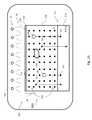
- FIGS. 1A-1Eare diagrams illustrating vacancy injected gettering for a semiconductor wafer for one embodiment of the present disclosure
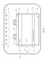
- FIG. 2is a diagram illustrating backsurface field formation for a semiconductor device of one embodiment of the present disclosure
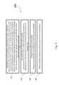
- FIG. 3is a flow chart illustrating a method for back-firing of one embodiment of the present disclosure
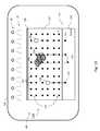
- FIGS. 4A-4Care diagrams illustrating front-firing for a semiconductor device of one embodiment of the present disclosure.
- FIG. 5is a flow chart illustrating a method for front-firing of one embodiment of the present disclosure.
- Embodiments of the present disclosureprovide for semiconductor device fabrication techniques using multiple firing processes as discussed below.
- the temperatures needed to dissolve precipitated impuritiesare high, and need to be applied for extended durations.
- many common precipitated impuritiessuch as iron silicide
- the precipitated impurityneeds to be allowed to expand to occupy a greater volume.
- the crystal lattice structureprohibits such expansion unless the temperature of the lattice is quite high.
- One embodiment of the present disclosurecomprises a first “back firing” process followed by a subsequent “front firing” process.
- Back-firingcombines optimization of back contact properties with impurity gettering.
- One important property of a back contact layeris to create a field that can reflect minority carriers.
- vacancy injection getteringa process for injecting vacancies within the silicon wafer to act as getters.
- Si atoms within the crystal latticeare randomly replaced with vacancies.
- a semiconductor device 110comprises a Silicon (Si) semiconductor wafer 112 having an Aluminum (Al) contact layer 114 .
- the Al contact layer 114comprises one or more layers of an Al ink material applied to a back surface of the Si wafer 112 to form an interface 113 between the Si layer 112 and Al contact layer 114 .
- the Si wafer 112comprises a crystalline lattice 120 of Si atoms 121 .
- Si layer 112may also include one or more dissolved impurities (shown as 124 ) as well as one or more predicated impurities (shown as 126 ).
- N-Type diffusionsuch as a phosphorus diffusion, for example
- dopant source materialsuch as P 2 O 5 , for example
- the dopant sourceis removed, and the dopant is diffused deeper into the silicon layer 112 (for example, by using a during a high-temperature limited-source diffusion (or “drive-in”) step).
- An anti-reflective layer 136(such as one comprising Silicon Nitrite SiN:H for example) may also be applied over the front surface 115 .
- the N+ diffusion process drive-in stepcan also be done concurrently with the application of the anti-reflexive layer 136 and/or prior to, after, or during back-firing.
- semiconductor device 110is optically processed within a chamber 106 of an optical furnace 105 .
- optical furnace 105Further details regarding different example embodiments of such an optical furnace may be found in any of U.S. Pat. No. 5,577,157 (entitled “Optical Processing Furnace with Quartz Muffle and Diffuser Plate” issued Nov. 19, 1996), U.S. Pat. No. 6,852,371 (entitled “Metal Processing for Impurity Gettering in Silicon” issued Feb. 8, 2005), and U.S. Patent Publication 2011/003485 (entitled “Optical Cavity Furnace for Semiconductor Wafer Processing” published Jan. 6, 2011), which are each incorporated herein by reference in their entirety.
- optically processingmay be performed one wafer at a time, or in discrete batches of multiple wafers depending on the holding capacity of the optical furnace being used, or in other configurations.
- Light sources 21 within the furnacewould be controlled to achieve an application of optical energy 25 having the desired intensity profile.
- the light sources 21are segmented into three regions 152 , 154 and 156 , such as shown in FIG. 1D .
- region 152is designated “Front/Back”
- region 154is designated “Right/Left”
- region 156is designated “Center.”
- region 152is designated “Front/Back”
- region 154is designated “Right/Left”
- region 156is designated “Center.”
- One of ordinary skill in the artwould recognize that other implementations may comprise alternate configurations and/or segmentations of light sources 21 . In the implementation shown in FIG.
- each of the regions 152 , 154 and 156have an associated controller (shown as respective controllers 153 , 155 and 157 ) which regulate and control the power delivered to the light sources 21 within the respective regions.
- the power delivered by the controllers 153 , 155 and 157 to light sources 21is coordinated to provide an optical flux within optical cavity furnace 105 that produces a uniform temperature over semiconductor device 110 .
- injected vacanciesare introduced into Si layer 112 at the interface 113 between the Si layer 112 and the Al layer 114 .
- a vacancy 128refers to a missing Si atom 121 within the structure of crystal lattice 120 .
- a vacancy 128“moves” through the crystal lattice 120 as Si atoms 121 shuffle positions within the lattice 120 .
- the processis initiated when optical energy 25 is applied to the semiconductor device 110 causing some of the Si atoms 121 , from random locations within the Si layer 112 , to diffuse into the Al layer 114 .
- the Si atoms 121 that migrate from the Si layer 112 into the Al contact layer 114each leave behind a vacancy 128 within the lattice 120 .
- Al atomsdo not migrate into the Si layer 112 from the Al layer 114 in a reciprocal manner. Thus the net result is an increase in the number of vacancies 128 within the Si layer 112 's lattice 120 .
- precipitated impurities 126may then expand within lattice 120 .
- precipitated impurity 126dissolves into a plurality of dissolved impurities 124 (as shown in FIG. 1C ) and will migrate into Al layer 114 , as shown generally at 125 . That is, once in a dissolved form, the impurities 124 diffuse into and become trapped within the Al contact layer 114 . Remaining unused vacancies 128 , through the shuffling of Si atoms 121 within the crystal lattice 120 , eventually dissipate.
- optical energy 25 reaching the Si—Al layer interface 113should be controlled to remain within a range that promotes diffusion across the interface 113 and avoids liquidation of Si.
- a liquid alloy of Si and Alwill form at the interface 113 causing liquid Si to flow along the interface 113 . If this condition occurs, the resulting liquid alloy will not allow any further diffusion of atoms from the Si layer 112 to cross into the Al contact layer 114 .
- alloying of the Si and Alshould be avoided (at least for an initial duration of time) by regulating the optical energy 25 applied.
- FIG. 1Eillustrates one implementation of a set of time verses optical power profiles at 182 , 184 and 186 provided by light sources 21 for a front-firing process.
- controller 153controls power to light sources 21 in region 152 such that the optical energy 25 they output conforms to optical power profile 182 .
- Controller 155controls power to light sources 21 in region 154 such that the optical energy 25 they output conforms to optical power profile 184 .
- Controller 157controls power to light sources 21 in region 156 such that the optical energy 25 they output conforms to optical power profile 186 .
- the particular profiles 182 , 184 and 186are tailored so that light sources 21 provide an optical flux within optical cavity furnace 105 that produces a uniform temperature over semiconductor device 110 .
- These particular profilesare about 250 seconds in total duration and have a “ramping stage” 190 shaped to gradually ramp up temperature, followed by a “high-intensity stage” 195 which increases optical flux via one or more step changes to the intended maximum intensity for each region (i.e., I max1 , I max2 , and I max3 ).
- the ramping stage 190provides a gradual warm up in order to minimize localized thermally induced stresses and maintain a temperature at the interface below that at which liquidation of the semiconductor material (e.g. Si) occurs.
- the “high-intensity stage” 195completes backsurface field formation and also completes the process of fusing the Al material of Al contact layer 114 with the Si layer 112 to provide an electrode to the “back” P+ region of Si Layer 112 .
- performing vacancy injectionhas the unforeseen advantage of enabling the growth of a larger and better defined backsurface field 130 than can be achieved through co-firing processes. While injected vacancies 128 are being formed in Si layer 112 , and precipitated impurities 126 are being dissolved and then trapped within the Al layer 114 through diffusion, temperatures of the wafer 112 may be held at higher temperatures and for longer duration than possible during a co-firing process. This is possible because (unlike cofiring) there is no front metal present in this first firing step. In a cofiring process high temperature and long process times can cause the front metal to interact at the front surface and punch through the junction.
- the high-intensity stage 195applies a significantly higher intensity of optical energy to promote backsurface layer formation without adversely affecting the results of the vacancy injection.
- backsurface layer 130contributes to an increased efficiency for solar cell applications because the backsurface layer 130 establishes a P+ region within the Si layer 112 which reflects elections (e) that attempt to cross interface 113 .
- the heating generated during vacancy injection processhelps produce a thin layer of Si—Al eutectic at interface 113 immediately before the melting of Al occurs.
- This thin layer of Si—Al eutecticpromotes adhesion of liquid Al to the Si, thus allowing formation of a uniformly deep (i.e., thick) backsurface layer 130 at interface 113 .
- both the intended maximum intensities (I max1, 2, 3 . . . ) applied during the high-intensity stage 195 and the duration of high-intensity stage 195should be limited.
- Optical energy applied during the high-intensity stage 195can be increased in intensity to produce temperatures at interface 113 that exceed those that promote vacancy injection, but should be limited to avoid detrimental Al bleeding into Si layer 112 .
- the impurity gettering and backsurface field processes described abovecomprise what is referred to herein as a “back-firing process” because they are each performed in conjunction with the process of fusing the Al material of Al contact layer 114 with the Si layer 112 to provide an electrode to the “back” P+ region of Si layer 112 .
- FIG. 3provides a flow chart illustration of one embodiment of a back-firing process shown as method 300 .
- Method 300may be implemented in accordance with any combination of the steps or processes described above with respect to FIGS. 1A-1D and 2 .
- Method 300begins at 310 with applying a first optical energy to a semiconductor wafer comprising a semiconductor layer and a metallic back-contact material layer, wherein the first optical energy is oriented to penetrate the semiconductor layer to the metallic back-contact material layer, and wherein the first optical energy is controlled to match a first intensity profile that produces a uniform heating along an interface within the semiconductor wafer between the semiconductor layer and the metallic back-contact material layer.
- the semiconductormay include a diffused N-P junction.
- the semiconductor layercomprises a Silicon layer while the back-contact material layer comprises an Aluminum or Aluminum precursor (such as an Al ink) layer. In one embodiment, this is accomplished by optical processing of the semiconductor wafer in an optical furnace such as discussed above.
- the optical energy appliedshould be controlled so that at the Si—Al layer interface liquidation of Si is avoided in the initial part of the flux-time profile.
- the optical energy applied during optical energy profile 310results in the temperature at the Si—Al interface being too high, a liquid alloy of Si and Al will form at the interface and causing liquid Si to flow along the interface. If this undesirable condition occurs, the resulting liquid alloy will not allow any diffusion of atoms from the Si layer to cross into the Al contact layer.
- alloying of the Si and Alshould be avoided by regulating the duration and shape of the first optical energy profile.
- applying the first optical energy profilemay further comprise controlling the optical energy received at an interface between the semiconductor layer and the Al material to maintain a temperature at the interface below that at which liquidation of the semiconductor material (e.g., Si) occurs.
- optical power profiles provided by light sources 21are controlled such as shown with respect to FIG. 1D . Profiles for different regions of light sources 21 are tailored so that light sources 21 provide an optical flux within optical cavity furnace 105 that produces a uniform temperature over semiconductor device 110 . These particular profiles are about 225 seconds in total duration and shaped to gradually ramp up temperature and then increase optical flux in one or more step changes to the intended maximum intensity for each region (i.e., I max1 , I max2 , and I max3 ).
- the ramping stageprovides a gradual warm up of the furnace parts (if the furnace is started from cold) and prevents any thermal shock. Because the wafer 112 is heated isothermally, wafer breakage is not an issue. The temperature of the wafer during the ramp-up is maintained such that the temperature at the interface 113 is below that at which liquidation of the semiconductor material (e.g., Si) occurs.
- the methodincludes injecting vacancies into a crystalline lattice of the semiconductor layer by diffusing atoms (for example, Si atoms) of the semiconductor material into the metallic back-contact material layer (shown at 320 ). This process creates a composition at the interface that can generate a silicon-aluminum alloy of a low melting point.
- the optical poweris then increased rather rapidly to create a molten alloy at the interface.
- the composition of the alloychanges as the temperature is increased (becoming richer in silicon at higher temperatures).
- a thick layer of molten alloy at the interfacewhich is rich in silicon (indicated by block 330 ).
- the vacancies injectioncontinues, while silicon interstitials are used up at the molten interface.
- the formation of the backsurface fieldoccurs during the ramp-down part of the process cycle (shown at block 340 ).
- the silicon with the highest dopant concentrationsolidifies first as an epitaxial layer.
- the doped siliconcontinues to grow forming a back surface field layer.
- the entire meltfreezes as an alloy.
- back-fire processingmay by proceeded by performing a dopant diffusion (such as the N-Type diffusion described above) onto a front surface of the semiconductor layer.
- a dopant diffusionsuch as the N-Type diffusion described above
- the semiconductor layeris transformed by the method into a material having an N+ region at its front surface, a P+ region at its back surface and a P region between the N+ and P+ regions.
- the methodmay also include (or be proceeded or followed by) applying an anti-reflective material layer to the front surface region of the semiconductor layer (e.g., over the N+ silicon region formed).
- semiconductor device 110is further configured with a patterned layer of front side metallic conducting material 410 (such as a Silver (Ag) ink, for example). This metallic conducting material would be applied, for example, over an SiN anti-reflective coating layer (such as anti-reflective coating layer 136 ).
- front side metallic conducting material 410such as a Silver (Ag) ink, for example. This metallic conducting material would be applied, for example, over an SiN anti-reflective coating layer (such as anti-reflective coating layer 136 ).
- optical energy 25 from the bank of light sources 21is applied to heat the front side metallic conducting material 410 , causing the metallic conducting material 410 to etch through anti-reflective coating layer 136 and form a mechanical and electrical bond with the N+ region 134 of Si layer 112 (as shown in FIG. 4B ).
- the optical energyis applied at lower intensity and for a shorter duration of time as compared to back-firing, such that it does not affect the results obtained from the prior back-firing.
- the metallic conducting material 410 forming the electrical connection to N+ region 134should be patterned accordingly to permit a sufficient number of photons to penetrate into Si layer 112 .
- the resulting semiconductor device 420 shown in FIG. 4Bthus provides an electrical device having a P-N junction suitable for photovoltaic (PV) applications.
- FIG. 4Cillustrates one implementation of a set of time verses optical power profiles at 482 , 484 and 486 provided by light sources 21 with respect to a front-firing process.
- the particular profiles 482 , 484 and 486are tailored so that light sources 21 provide an optical flux within optical cavity furnace 105 that produces a uniform temperature over semiconductor device 110 .
- the optical energy applied by profiles 482 , 484 and 486are tailored to result in lower temperatures within the semiconductor wafer than produced by profiles 182 , 184 and 186 .
- optical energy applied by profiles 482 , 484 and 486have a much shorter duration in the region 495 (ie, beyond the 210 second mark) than profiles 182 , 184 and 186 .
- the duration of the highest fluxcan be less than 10 seconds, compared to about 40 seconds during back-firing. As such, the results achieved during the back-firing process are not adversely affected by the front firing process.
- a ramping stage 490provides a gradual warm up in order to minimize localized thermally induced stresses.
- the “high-intensity stage” 495completes the firing of the metallic conducting material 410 to semiconductor layer 112 .
- the optical energy applied by profiles 482 , 484 and 486has a duration of about 1 second and produces a peak temperature in the range of 800 to 850 degrees at the front side 115 of Si layer 112 .
- FIGS. 4A-4Ccomprise what is referred to herein as a “front-firing process” because they are each performed as part of the process of fusing electrical connections 410 to the front side 115 of Si layer 112 .
- a front-firing processis illustrated with respect to the method 500 illustrated in FIG. 5 , which may be implemented in accordance with any combination of the steps or processes described above with respect to FIGS. 4A-4C and optionally in conjunction with an optical furnace such as disclosed in U.S. Pat. No. 5,577,157 incorporated herein by reference in its entirety.
- Method 500follows method 300 and begins at 510 with depositing a patterned layer of a metallic conducting material over an anti-reflective coating layer of the semiconductor wafer. In one embodiment, this comprises depositing a patterned layer of a Silver (Ag) ink, for example, over an SiN anti-reflective coating layer of the semiconductor wafer. The method then proceeds to 520 with applying a second optical energy to the semiconductor wafer, wherein the second optical energy is controlled to match a second intensity profile that produces a uniform heating between the layer of metallic conducting material and the anti-reflective coating layer.
- a patterned layer of a metallic conducting materialover an anti-reflective coating layer of the semiconductor wafer.
- thiscomprises depositing a patterned layer of a Silver (Ag) ink, for example, over an SiN anti-reflective coating layer of the semiconductor wafer.
- the methodthen proceeds to 520 with applying a second optical energy to the semiconductor wafer, wherein the second optical energy is controlled to match a second intensity profile that produces a uniform heating
- the optical energy applied by the second optical energy profile during the front-firing processwill produce lower temperatures within the semiconductor wafer and have a much shorter duration than the first optical energy profile so that the structures established by the back-firing process are not adversely affected by the front firing process.
- other temperature profilesmay be tailored based on the materials used for the metallic conducting material.
Landscapes
- Photovoltaic Devices (AREA)
Abstract
Description
The United States Government has rights in this invention under Contract No. DE-AC36-08GO28308 between the United States Department of Energy and the Alliance for Sustainable Energy, LLC, the Manager and Operator of the National Renewable Energy Laboratory.
Photovoltaic solar cell fabrication often involves the process of “co-firing” where metallic electrical conductors are mechanically and electrically coupled to semiconductor materials to create an electrical p-n semiconductor photovoltaic device. For example, during fabrication, an aluminum (Al) “ink” would be applied to a back surface (e.g., a p-type region) of a wafer of semiconductor material (such as a Silicon (Si) wafer). The opposing front surface (e.g. an n-type region layer) of the wafer would have a coating of silicon nitride (SiN) applied and a pattern of silver (Ag) “ink” applied over the SiN. The device is then fired (that is, heated in a furnace) such that the Ag ink dissolves through portions of the SiN layer to make electrical contact with the n-type region and the Al and Si at the back surface dissolve and then re-grow to form a good electrical and mechanical connection.
One problem associated with the fabrication of a photovoltaic solar cell involves the purity level of a semiconductor (e.g. Si) material. The purity level is often a function of the production facility used. That is, production of semiconductors wafers with little to no impurities usually requires tightly controlled clean-room environments. For industrial facilities attempting to produce Si wafers on a mass-production scale for photovoltaic solar cell devices, maintaining strict clean-room environments is economically prohibitive. Therefore, some degree of impurities can be expected to exist in the final fabricated wafers. Such industrial facilities may therefore employ one or more post-processing techniques to attempt to rid impurities from the wafers. For example, if Si layers of a photovoltaic device include dissolved (that is, non-precipitated) impurities within the silicon material, then optical processing can be used to cleanse the wafer. Under optical processing, a diffusion process (called gettering) can be initiated that will cause the dissolved impurities to migrate into the Aluminum contact material. For example, by initiating diffusion, dissolved iron (Fe) impurities can rapidly (i.e., in the matter of a few minutes) be removed from the Si layers. This serves to clean impurities from the silicon wafer. A problem occurs however, when the impurities include precipitated material. In that case, diffusion will not cause movement of the precipitated impurities from the silicon layers. Further, the durations and high temperatures required to dissolve the precipitate impurities may not be compatible with other co-firing process steps, and have the potential to increase manufacturing expenses.
Embodiments described herein can be more easily understood and further advantages and uses thereof more readily apparent, when considered in view of this description and the following figures in which:
In accordance with common practice, the various described features are not drawn to scale but are drawn to emphasize relevant features. Reference characters denote like elements throughout Figures and text.
Embodiments of the present disclosure provide for semiconductor device fabrication techniques using multiple firing processes as discussed below. Typically, the temperatures needed to dissolve precipitated impurities are high, and need to be applied for extended durations. Further, because many common precipitated impurities (such as iron silicide) expand in volume as they dissolve, the precipitated impurity needs to be allowed to expand to occupy a greater volume. However, when a precipitated impurity is locked within the structure of a crystal lattice, (as would be the case for a precipitated impurity within a Si wafer), the crystal lattice structure prohibits such expansion unless the temperature of the lattice is quite high. While heating of the crystal lattice will cause the atoms of the lattice to vibrate, creating some room for expansion of the precipitated impurity, the durations and high temperatures required to dissolve the precipitate impurities may not be compatible with other co-firing process steps, and have the potential to increase manufacturing expenses. Embodiments described in the present disclosure address this objective technical problem by introducing multi-firing semiconductor device fabrication techniques as an alternative to traditional co-firing. These embodiments are described in greater detail with reference to the accompanying Figures.
One embodiment of the present disclosure comprises a first “back firing” process followed by a subsequent “front firing” process. Back-firing combines optimization of back contact properties with impurity gettering. One important property of a back contact layer is to create a field that can reflect minority carriers. As will be further discussed below, the inventors have found that formation of this field is strongly compatible with vacancy injection gettering—a process for injecting vacancies within the silicon wafer to act as getters. In vacancy injection, Si atoms within the crystal lattice are randomly replaced with vacancies. These vacancies, when situated in the proximity of a precipitate impurity, provide room for expansion which permits the precipitated impurity to dissolve at lower temperatures than possible without the vacancies. Once the impurity is converted into a dissolved state, diffusion takes over to remove the impurity from the silicon wafer. Vacancy injection is discussed further in U.S. Pat. No. 6,852,371 (entitled “Metal Processing for Impurity Gettering in Silicon” and issued Feb. 8, 2005) which is incorporated herein by reference in its entirety.
As illustrated inFIG. 1A , asemiconductor device 110 comprises a Silicon (Si)semiconductor wafer 112 having an Aluminum (Al)contact layer 114. In one embodiment, theAl contact layer 114 comprises one or more layers of an Al ink material applied to a back surface of theSi wafer 112 to form aninterface 113 between theSi layer 112 andAl contact layer 114. The Siwafer 112 comprises acrystalline lattice 120 ofSi atoms 121.Si layer 112 may also include one or more dissolved impurities (shown as124) as well as one or more predicated impurities (shown as126).
Prior to back-firing, one or more preliminary fabrication step are typically performed onwafer 112. For example, N-Type diffusion (such as a phosphorus diffusion, for example) may be employed to apply a thin layer of dopant source material (such as P2O5, for example) onto afront surface 115 ofSi layer 112, which provides elemental material for diffusion intoSi layer 112. This results in an N+ region (shown at134) of Si material. For some embodiments, after a desired amount of dopant is deposited on thefront surface 115 ofsilicon layer 112, the dopant source is removed, and the dopant is diffused deeper into the silicon layer112 (for example, by using a during a high-temperature limited-source diffusion (or “drive-in”) step). Ananti-reflective layer 136, (such as one comprising Silicon Nitrite SiN:H for example) may also be applied over thefront surface 115. In alternate embodiments, the N+ diffusion process drive-in step can also be done concurrently with the application of theanti-reflexive layer 136 and/or prior to, after, or during back-firing.
To purge dissolvedimpurities 124 fromSi layer 112,semiconductor device 110 is optically processed within achamber 106 of anoptical furnace 105. Further details regarding different example embodiments of such an optical furnace may be found in any of U.S. Pat. No. 5,577,157 (entitled “Optical Processing Furnace with Quartz Muffle and Diffuser Plate” issued Nov. 19, 1996), U.S. Pat. No. 6,852,371 (entitled “Metal Processing for Impurity Gettering in Silicon” issued Feb. 8, 2005), and U.S. Patent Publication 2011/003485 (entitled “Optical Cavity Furnace for Semiconductor Wafer Processing” published Jan. 6, 2011), which are each incorporated herein by reference in their entirety. In different implementations, optically processing may be performed one wafer at a time, or in discrete batches of multiple wafers depending on the holding capacity of the optical furnace being used, or in other configurations.
By applying the back-firing processing techniques described herein, injected vacancies (shown at128 ofFIG. 1A ) are introduced intoSi layer 112 at theinterface 113 between theSi layer 112 and theAl layer 114. As the term is used herein, avacancy 128 refers to a missingSi atom 121 within the structure ofcrystal lattice 120. Avacancy 128 “moves” through thecrystal lattice 120 asSi atoms 121 shuffle positions within thelattice 120. The process is initiated whenoptical energy 25 is applied to thesemiconductor device 110 causing some of theSi atoms 121, from random locations within theSi layer 112, to diffuse into theAl layer 114. TheSi atoms 121 that migrate from theSi layer 112 into theAl contact layer 114 each leave behind avacancy 128 within thelattice 120. Note that Al atoms do not migrate into theSi layer 112 from theAl layer 114 in a reciprocal manner. Thus the net result is an increase in the number ofvacancies 128 within theSi layer 112'slattice 120.
As illustrated inFIG. 1B , whenvacancies 128 are formed proximate to a precipitatedimpurity 126, the precipitatedimpurities 126 may then expand withinlattice 120. Provided this room to expand in the presence ofoptical energy 25, precipitatedimpurity 126 dissolves into a plurality of dissolved impurities124 (as shown inFIG. 1C ) and will migrate intoAl layer 114, as shown generally at125. That is, once in a dissolved form, theimpurities 124 diffuse into and become trapped within theAl contact layer 114. Remainingunused vacancies 128, through the shuffling ofSi atoms 121 within thecrystal lattice 120, eventually dissipate.
It should be noted that during a first stage of the optical processing,optical energy 25 reaching the Si—Al layer interface 113 should be controlled to remain within a range that promotes diffusion across theinterface 113 and avoids liquidation of Si. In other words, when the optical energy applied at the Si—Al interface 113 is too high, a liquid alloy of Si and Al will form at theinterface 113 causing liquid Si to flow along theinterface 113. If this condition occurs, the resulting liquid alloy will not allow any further diffusion of atoms from theSi layer 112 to cross into theAl contact layer 114. Thus alloying of the Si and Al should be avoided (at least for an initial duration of time) by regulating theoptical energy 25 applied.
Theparticular profiles light sources 21 provide an optical flux withinoptical cavity furnace 105 that produces a uniform temperature oversemiconductor device 110. These particular profiles are about 250 seconds in total duration and have a “ramping stage”190 shaped to gradually ramp up temperature, followed by a “high-intensity stage”195 which increases optical flux via one or more step changes to the intended maximum intensity for each region (i.e., Imax1, Imax2, and Imax3). The rampingstage 190 provides a gradual warm up in order to minimize localized thermally induced stresses and maintain a temperature at the interface below that at which liquidation of the semiconductor material (e.g. Si) occurs. The “high-intensity stage”195 completes backsurface field formation and also completes the process of fusing the Al material ofAl contact layer 114 with theSi layer 112 to provide an electrode to the “back” P+ region ofSi Layer 112.
As explained with reference toFIG. 2 , in addition to cleansingimpurities Si layer 112, performing vacancy injection has the unforeseen advantage of enabling the growth of a larger and better definedbacksurface field 130 than can be achieved through co-firing processes. While injectedvacancies 128 are being formed inSi layer 112, and precipitatedimpurities 126 are being dissolved and then trapped within theAl layer 114 through diffusion, temperatures of thewafer 112 may be held at higher temperatures and for longer duration than possible during a co-firing process. This is possible because (unlike cofiring) there is no front metal present in this first firing step. In a cofiring process high temperature and long process times can cause the front metal to interact at the front surface and punch through the junction. However, in various embodiments described herein, such higher temperatures are very favorable for forming a highquality backsurface layer 130. Once a sufficient amount of time has elapsed to achieve the desired level of vacancy injected getterring, the high-intensity stage 195 applies a significantly higher intensity of optical energy to promote backsurface layer formation without adversely affecting the results of the vacancy injection.
An increased thickness ofbacksurface layer 130 contributes to an increased efficiency for solar cell applications because thebacksurface layer 130 establishes a P+ region within theSi layer 112 which reflects elections (e) that attempt to crossinterface 113. The heating generated during vacancy injection process helps produce a thin layer of Si—Al eutectic atinterface 113 immediately before the melting of Al occurs. This thin layer of Si—Al eutectic promotes adhesion of liquid Al to the Si, thus allowing formation of a uniformly deep (i.e., thick)backsurface layer 130 atinterface 113. The longer the vacancy injection process is permitted to continue, thethicker backsurface layer 130 will grow. There is a limit, however, on the thickness of thebacksurface layer 130 that can be achieved because if the process is allowed to continue too long, Al material fromlayer 114 may begin to pass throughSi layer 112 at some localized spots, where material can have defects such as multiple grain boundaries. If this occurs long enough to permit a sufficient amount of Al material to pass throughSi layer 112, the ability forsemiconductor device 110 to function as part of a solar cell is destroyed. Accordingly, both the intended maximum intensities (Imax1, 2, 3 . . .) applied during the high-intensity stage 195 and the duration of high-intensity stage 195 should be limited. Optical energy applied during the high-intensity stage 195 can be increased in intensity to produce temperatures atinterface 113 that exceed those that promote vacancy injection, but should be limited to avoid detrimental Al bleeding intoSi layer 112. The impurity gettering and backsurface field processes described above comprise what is referred to herein as a “back-firing process” because they are each performed in conjunction with the process of fusing the Al material ofAl contact layer 114 with theSi layer 112 to provide an electrode to the “back” P+ region ofSi layer 112.
As mentioned above the optical energy applied should be controlled so that at the Si—Al layer interface liquidation of Si is avoided in the initial part of the flux-time profile. In other words, when the optical energy applied duringoptical energy profile 310 results in the temperature at the Si—Al interface being too high, a liquid alloy of Si and Al will form at the interface and causing liquid Si to flow along the interface. If this undesirable condition occurs, the resulting liquid alloy will not allow any diffusion of atoms from the Si layer to cross into the Al contact layer. Thus alloying of the Si and Al should be avoided by regulating the duration and shape of the first optical energy profile. Accordingly, applying the first optical energy profile may further comprise controlling the optical energy received at an interface between the semiconductor layer and the Al material to maintain a temperature at the interface below that at which liquidation of the semiconductor material (e.g., Si) occurs. For example, in one embodiment, optical power profiles provided bylight sources 21 are controlled such as shown with respect toFIG. 1D . Profiles for different regions oflight sources 21 are tailored so thatlight sources 21 provide an optical flux withinoptical cavity furnace 105 that produces a uniform temperature oversemiconductor device 110. These particular profiles are about 225 seconds in total duration and shaped to gradually ramp up temperature and then increase optical flux in one or more step changes to the intended maximum intensity for each region (i.e., Imax1, Imax2, and Imax3). The ramping stage provides a gradual warm up of the furnace parts (if the furnace is started from cold) and prevents any thermal shock. Because thewafer 112 is heated isothermally, wafer breakage is not an issue. The temperature of the wafer during the ramp-up is maintained such that the temperature at theinterface 113 is below that at which liquidation of the semiconductor material (e.g., Si) occurs. During this ramping stage, the method includes injecting vacancies into a crystalline lattice of the semiconductor layer by diffusing atoms (for example, Si atoms) of the semiconductor material into the metallic back-contact material layer (shown at320). This process creates a composition at the interface that can generate a silicon-aluminum alloy of a low melting point.
The optical power is then increased rather rapidly to create a molten alloy at the interface. The composition of the alloy changes as the temperature is increased (becoming richer in silicon at higher temperatures). At the target maximum intensity, a thick layer of molten alloy at the interface, which is rich in silicon (indicated by block330). During this period, the vacancies injection continues, while silicon interstitials are used up at the molten interface. The formation of the backsurface field occurs during the ramp-down part of the process cycle (shown at block340). During the cooldown, the silicon with the highest dopant concentration solidifies first as an epitaxial layer. As the temperature of the wafer reduces, the doped silicon continues to grow forming a back surface field layer. Finally, the entire melt freezes as an alloy.
As mentioned above, back-fire processing may by proceeded by performing a dopant diffusion (such as the N-Type diffusion described above) onto a front surface of the semiconductor layer. In that case, the semiconductor layer is transformed by the method into a material having an N+ region at its front surface, a P+ region at its back surface and a P region between the N+ and P+ regions. The method may also include (or be proceeded or followed by) applying an anti-reflective material layer to the front surface region of the semiconductor layer (e.g., over the N+ silicon region formed).
After the back-firing process described inFIG. 3 , the front firing process is subsequently performed to provide electrodes on thefront surface 115Si Layer 112. This is illustrated by reference toFIGS. 4A-4B . Referring first toFIG. 4A ,semiconductor device 110 is further configured with a patterned layer of front side metallic conducting material410 (such as a Silver (Ag) ink, for example). This metallic conducting material would be applied, for example, over an SiN anti-reflective coating layer (such as anti-reflective coating layer136). Again using optical processing such as described above,optical energy 25 from the bank oflight sources 21 is applied to heat the front sidemetallic conducting material 410, causing themetallic conducting material 410 to etch throughanti-reflective coating layer 136 and form a mechanical and electrical bond with theN+ region 134 of Si layer112 (as shown inFIG. 4B ). During front-firing, the optical energy is applied at lower intensity and for a shorter duration of time as compared to back-firing, such that it does not affect the results obtained from the prior back-firing. As would be appreciated by one of ordinary skill in the art upon reading this disclosure, for PV applications, themetallic conducting material 410 forming the electrical connection toN+ region 134 should be patterned accordingly to permit a sufficient number of photons to penetrate intoSi layer 112. The resultingsemiconductor device 420 shown inFIG. 4B thus provides an electrical device having a P-N junction suitable for photovoltaic (PV) applications.
These process steps described with respect toFIGS. 4A-4C comprise what is referred to herein as a “front-firing process” because they are each performed as part of the process of fusingelectrical connections 410 to thefront side 115 ofSi layer 112. One embodiment of such a front-firing process is illustrated with respect to themethod 500 illustrated inFIG. 5 , which may be implemented in accordance with any combination of the steps or processes described above with respect toFIGS. 4A-4C and optionally in conjunction with an optical furnace such as disclosed in U.S. Pat. No. 5,577,157 incorporated herein by reference in its entirety.
Although specific embodiments have been illustrated and described herein, it will be appreciated by those of ordinary skill in the art than any arrangement, which is calculated to achieve the same purpose may be substituted for the specific embodiments shown. This application is intended to cover any adaptations or variations. Therefore, it is manifestly intended that this application be limited only by the claims and the equivalents thereof.
Claims (21)
1. A method for fabricating an electrical semiconductor device, the method comprising:
applying a first optical energy to a semiconductor wafer comprising a semiconductor layer and a metallic back-contact material layer, wherein the first optical energy is oriented to penetrate the semiconductor layer to the metallic back-contact material layer, and wherein the first optical energy is controlled to match a first intensity profile that produces a uniform heating along an interface within the semiconductor wafer between the semiconductor layer and the metallic back-contact material layer;
during application of the first optical energy:
injecting vacancies into a crystalline lattice of the semiconductor layer by diffusing atoms of the semiconductor material into the metallic back-contact material layer; and
melting an interfacial layer comprising silicon and Al alloy at the interface;
during a cooldown, forming a backsurface field from the interfacial layer;
after the cooldown:
depositing a patterned layer of a metallic conducting material over an anti-reflective coating layer of the semiconductor wafer;
applying a second optical energy to the semiconductor wafer, wherein the second optical energy is controlled to match a second intensity profile that produces a uniform heating between the layer of metallic conducting material and the anti-reflective coating layer; and
during application of the second optical energy, firing the metallic conducting material through the anti-reflective coating layer to form a mechanical and electrical bond between the metallic conducting material and the semiconductor layer.
2. The method ofclaim 1 , wherein the semiconductor device comprises a Si wafer, and the metallic back-contact material layer comprises an Al ink material.
3. The method ofclaim 1 , further comprising performing a dopant diffusion onto a front surface of the semiconductor layer.
4. The method ofclaim 3 , wherein the dopant diffusion comprises an N-Type diffusion.
5. The method ofclaim 1 , wherein applying the first optical energy and the second optical energy is performed within an optical cavity furnace.
6. The method ofclaim 1 further comprising:
applying the anti-reflective material layer to a front surface region of the semiconductor layer.
7. The method ofclaim 1 wherein the anti-reflective material layer comprises an SiN anti-reflective coating layer.
8. The method ofclaim 1 , wherein the metallic conducting material comprises a Silver (Ag) ink material.
9. The method ofclaim 1 , wherein firing the metallic conducting material through the anti-reflective coating layer forms a mechanical and electrical bond between the metallic conducting material and a doped region of the semiconductor layer.
10. The method ofclaim 1 , wherein temperatures produced within the semiconductor wafer by the second optical energy are less than temperatures produced within the semiconductor wafer by the first optical energy.
11. A method for fabricating an electrical device having a P-N junction, the method comprising:
providing a semiconductor wafer comprising a semiconductor layer and a metallic back-contact material layer;
performing a back-firing process on the semiconductor wafer, the back-firing process comprising:
applying a first optical energy to a semiconductor wafer comprising a semiconductor layer and a metallic back-contact material layer, wherein the first optical energy is oriented to penetrate the semiconductor layer to the metallic back-contact material layer, and wherein the first optical energy is controlled to match a first intensity profile that produces a uniform heating along an interface within the semiconductor wafer between the semiconductor layer and the metallic back-contact material layer;
injecting vacancies into a crystalline lattice of the semiconductor layer by diffusing atoms of the semiconductor material into the metallic back-contact material layer; and
forming a backsurface field between the semiconductor layer and the metallic back-contact material layer;
after the back-firing process, performing a front-firing process on the semiconductor wafer, the front-firing process comprising:
applying a second optical energy to the semiconductor wafer, wherein the second optical energy is controlled to match a second intensity profile that produces a uniform heating between a layer of metallic conducting material and an anti-reflective coating layer; and
during application of the second optical energy, firing a metallic conducting material through the anti-reflective coating layer to form a mechanical and electrical bond between the metallic conducting material and the semiconductor layer.
12. The method ofclaim 11 , wherein the semiconductor layer comprises a Si layer, and the metallic back-contact material layer comprises an Al ink material.
13. The method ofclaim 11 , wherein the semiconductor layer comprises an N-type region and a P-type region.
14. The method ofclaim 11 , further comprising performing a dopant diffusion onto a front surface of the semiconductor layer.
15. The method ofclaim 14 , wherein the dopant diffusion comprises an N-Type diffusion.
16. The method ofclaim 11 further comprising:
applying the anti-reflective material layer to a front surface region of the semiconductor layer.
17. The method ofclaim 11 , wherein the anti-reflective material layer comprises an SiN anti-reflective coating layer.
18. The method ofclaim 11 , wherein the metallic conducting material comprises a Silver (Ag) ink material.
19. The method ofclaim 11 , wherein firing the metallic conducting material through the anti-reflective coating layer forms a mechanical and electrical bond between the metallic conducting material and a doped region of the semiconductor layer.
20. The method ofclaim 11 , wherein temperatures produced within the semiconductor wafer by the second optical energy are less than temperatures produced within the semiconductor wafer by the first optical energy.
21. The method ofclaim 11 , wherein injecting vacancies further comprises diffusing atoms of the semiconductor material into a Si—Al melt.
Priority Applications (1)
| Application Number | Priority Date | Filing Date | Title |
|---|---|---|---|
| US13/744,152US8735204B1 (en) | 2013-01-17 | 2013-01-17 | Contact formation and gettering of precipitated impurities by multiple firing during semiconductor device fabrication |
Applications Claiming Priority (1)
| Application Number | Priority Date | Filing Date | Title |
|---|---|---|---|
| US13/744,152US8735204B1 (en) | 2013-01-17 | 2013-01-17 | Contact formation and gettering of precipitated impurities by multiple firing during semiconductor device fabrication |
Publications (1)
| Publication Number | Publication Date |
|---|---|
| US8735204B1true US8735204B1 (en) | 2014-05-27 |
Family
ID=50736416
Family Applications (1)
| Application Number | Title | Priority Date | Filing Date |
|---|---|---|---|
| US13/744,152Expired - Fee RelatedUS8735204B1 (en) | 2013-01-17 | 2013-01-17 | Contact formation and gettering of precipitated impurities by multiple firing during semiconductor device fabrication |
Country Status (1)
| Country | Link |
|---|---|
| US (1) | US8735204B1 (en) |
Citations (30)
| Publication number | Priority date | Publication date | Assignee | Title |
|---|---|---|---|---|
| US5223453A (en) | 1991-03-19 | 1993-06-29 | The United States Of America As Represented By The United States Department Of Energy | Controlled metal-semiconductor sintering/alloying by one-directional reverse illumination |
| US5429985A (en) | 1994-01-18 | 1995-07-04 | Midwest Research Institute | Fabrication of optically reflecting ohmic contacts for semiconductor devices |
| US5452396A (en) | 1994-02-07 | 1995-09-19 | Midwest Research Institute | Optical processing furnace with quartz muffle and diffuser plate |
| US5627081A (en) | 1994-11-29 | 1997-05-06 | Midwest Research Institute | Method for processing silicon solar cells |
| US5693520A (en) | 1993-05-05 | 1997-12-02 | Novo Nordisk A/S | Recombinant trypsin-like protease |
| US5897331A (en) | 1996-11-08 | 1999-04-27 | Midwest Research Institute | High efficiency low cost thin film silicon solar cell design and method for making |
| US5928438A (en) | 1995-10-05 | 1999-07-27 | Ebara Solar, Inc. | Structure and fabrication process for self-aligned locally deep-diffused emitter (SALDE) solar cell |
| US6852371B2 (en) | 2000-03-03 | 2005-02-08 | Midwest Research Institute | Metal processing for impurity gettering in silicon |
| US20050239293A1 (en) | 2004-04-21 | 2005-10-27 | Zhenjiang Cui | Post treatment of low k dielectric films |
| US20050252544A1 (en) | 2004-05-11 | 2005-11-17 | Ajeet Rohatgi | Silicon solar cells and methods of fabrication |
| US20060208257A1 (en) | 2005-03-15 | 2006-09-21 | Branz Howard M | Method for low-temperature, hetero-epitaxial growth of thin film cSi on amorphous and multi-crystalline substrates and c-Si devices on amorphous, multi-crystalline, and crystalline substrates |
| US20070169685A1 (en) | 2006-01-20 | 2007-07-26 | Bp Corporation North America Inc. | Methods and Apparatuses for Manufacturing Geometric Multicrystalline Cast Silicon and Geometric Multicrystalline Cast Silicon Bodies for Photovoltaics |
| US7601215B1 (en) | 2006-11-17 | 2009-10-13 | Alliance For Sustainable Energy, Llc | Method for rapid, controllable growth and thickness, of epitaxial silicon films |
| US7645337B2 (en) | 2004-11-18 | 2010-01-12 | The Trustees Of Columbia University In The City Of New York | Systems and methods for creating crystallographic-orientation controlled poly-silicon films |
| US7670885B2 (en) | 2008-02-08 | 2010-03-02 | Advanced Lcd Technologies Development Center Co., Ltd. | Thin-film semiconductor device and method for manufacturing the same |
| US20100159676A1 (en) | 2008-12-23 | 2010-06-24 | Imec | Method For Manufacturing A Mono-Crystalline Semiconductor Layer on a Substrate |
| US20100193031A1 (en) | 2007-07-20 | 2010-08-05 | Bp Corporation North America Inc. | Methods and Apparatuses for Manufacturing Cast Silicon From Seed Crystals |
| US20100193016A1 (en) | 2006-08-22 | 2010-08-05 | Bp Solar Espana, S.A. Unipersonal | Photovoltaic Cell and Production Thereof |
| US20100193989A1 (en) | 2007-07-25 | 2010-08-05 | Bp Corporation North America Inc. | Methods Apparatus for Manufacturing Geometric Multi-Crystalline Cast Materials |
| US20100192838A1 (en) | 2007-07-25 | 2010-08-05 | Bp Corporation North America Inc. | Methods for Manufacturing Monocrystalline or Near-Monocrystalline Cast Materials |
| US7811900B2 (en) | 2006-09-08 | 2010-10-12 | Silicon Genesis Corporation | Method and structure for fabricating solar cells using a thick layer transfer process |
| US20110003485A1 (en) | 2008-03-13 | 2011-01-06 | Alliance For Sustainable Energy, Llc | Optical Cavity Furnace for Semiconductor Wafer Processing |
| US20110146782A1 (en)* | 2008-04-18 | 2011-06-23 | 1366 Technologies Inc. | Methods to pattern diffusion layers in solar cells and solar cells made by such methods |
| US20110197960A1 (en) | 2010-02-12 | 2011-08-18 | Heraeus Materials Technology Llc | Method for applying full back surface field and silver busbar to solar cell |
| US8012861B2 (en) | 2007-11-21 | 2011-09-06 | The Trustees Of Columbia University In The City Of New York | Systems and methods for preparing epitaxially textured polycrystalline films |
| US20110277682A1 (en) | 2008-07-22 | 2011-11-17 | Rana Virnedra V | Directional solid phase crystallization of thin amorphous silicon for solar cell applications |
| US8178221B2 (en) | 2000-07-10 | 2012-05-15 | Amit Goyal | {100}<100> or 45°-rotated {100}<100>, semiconductor-based, large-area, flexible, electronic devices |
| US8183081B2 (en) | 2008-07-16 | 2012-05-22 | Applied Materials, Inc. | Hybrid heterojunction solar cell fabrication using a metal layer mask |
| US8241941B2 (en) | 2008-07-09 | 2012-08-14 | Commissariat A L'energie Atomique | Method of purifying a crystalline silicon substrate and process for producing a photovoltaic cell |
| US20130087195A1 (en) | 2011-10-05 | 2013-04-11 | International Business Machines Corporation | Silicon solar cell with back surface field |
- 2013
- 2013-01-17USUS13/744,152patent/US8735204B1/ennot_activeExpired - Fee Related
Patent Citations (39)
| Publication number | Priority date | Publication date | Assignee | Title |
|---|---|---|---|---|
| US5223453A (en) | 1991-03-19 | 1993-06-29 | The United States Of America As Represented By The United States Department Of Energy | Controlled metal-semiconductor sintering/alloying by one-directional reverse illumination |
| US5693520A (en) | 1993-05-05 | 1997-12-02 | Novo Nordisk A/S | Recombinant trypsin-like protease |
| US5429985A (en) | 1994-01-18 | 1995-07-04 | Midwest Research Institute | Fabrication of optically reflecting ohmic contacts for semiconductor devices |
| US5452396A (en) | 1994-02-07 | 1995-09-19 | Midwest Research Institute | Optical processing furnace with quartz muffle and diffuser plate |
| US5577157A (en) | 1994-02-07 | 1996-11-19 | Midwest Research Institute | Optical processing furnace with quartz muffle and diffuser plate |
| US5627081A (en) | 1994-11-29 | 1997-05-06 | Midwest Research Institute | Method for processing silicon solar cells |
| US5928438A (en) | 1995-10-05 | 1999-07-27 | Ebara Solar, Inc. | Structure and fabrication process for self-aligned locally deep-diffused emitter (SALDE) solar cell |
| US5897331A (en) | 1996-11-08 | 1999-04-27 | Midwest Research Institute | High efficiency low cost thin film silicon solar cell design and method for making |
| US6201261B1 (en) | 1996-11-08 | 2001-03-13 | Midwest Research Institute | High efficiency, low cost, thin film silicon solar cell design and method for making |
| US6852371B2 (en) | 2000-03-03 | 2005-02-08 | Midwest Research Institute | Metal processing for impurity gettering in silicon |
| US8178221B2 (en) | 2000-07-10 | 2012-05-15 | Amit Goyal | {100}<100> or 45°-rotated {100}<100>, semiconductor-based, large-area, flexible, electronic devices |
| US20050239293A1 (en) | 2004-04-21 | 2005-10-27 | Zhenjiang Cui | Post treatment of low k dielectric films |
| US20080241986A1 (en) | 2004-05-11 | 2008-10-02 | Georgia Tech Research Corporation | Method for fabricating a silicon solar cell structure having amorphous silicon layers |
| US20050252544A1 (en) | 2004-05-11 | 2005-11-17 | Ajeet Rohatgi | Silicon solar cells and methods of fabrication |
| US7645337B2 (en) | 2004-11-18 | 2010-01-12 | The Trustees Of Columbia University In The City Of New York | Systems and methods for creating crystallographic-orientation controlled poly-silicon films |
| US20060208257A1 (en) | 2005-03-15 | 2006-09-21 | Branz Howard M | Method for low-temperature, hetero-epitaxial growth of thin film cSi on amorphous and multi-crystalline substrates and c-Si devices on amorphous, multi-crystalline, and crystalline substrates |
| US20120037066A1 (en) | 2006-01-20 | 2012-02-16 | Stoddard Nathan G | Methods and apparatus for manufacturing monocrystalline cast silicon and monocrystalline cast silicon bodies for photovoltaics |
| US8048221B2 (en) | 2006-01-20 | 2011-11-01 | Stoddard Nathan G | Methods and apparatuses for manufacturing monocrystalline cast silicon and monocrystalline cast silicon bodies for photovoltaics |
| US20120090537A1 (en) | 2006-01-20 | 2012-04-19 | Stoddard Nathan G | Methods and apparatus for manufacturing monocrystalline cast silicon and monocrystalline cast silicon bodies for photovoltaics |
| US20070169685A1 (en) | 2006-01-20 | 2007-07-26 | Bp Corporation North America Inc. | Methods and Apparatuses for Manufacturing Geometric Multicrystalline Cast Silicon and Geometric Multicrystalline Cast Silicon Bodies for Photovoltaics |
| US20120042947A1 (en) | 2006-01-20 | 2012-02-23 | Stoddard Nathan G | Methods and apparatus for manufacturing monocrystalline cast silicon and monocrystalline cast silicon bodies for photovoltaics |
| US20100193016A1 (en) | 2006-08-22 | 2010-08-05 | Bp Solar Espana, S.A. Unipersonal | Photovoltaic Cell and Production Thereof |
| US8110480B2 (en) | 2006-09-08 | 2012-02-07 | Silicon Genesis Corporation | Method and structure for fabricating solar cells using a thick layer transfer process |
| US7811900B2 (en) | 2006-09-08 | 2010-10-12 | Silicon Genesis Corporation | Method and structure for fabricating solar cells using a thick layer transfer process |
| US7601215B1 (en) | 2006-11-17 | 2009-10-13 | Alliance For Sustainable Energy, Llc | Method for rapid, controllable growth and thickness, of epitaxial silicon films |
| US20100193031A1 (en) | 2007-07-20 | 2010-08-05 | Bp Corporation North America Inc. | Methods and Apparatuses for Manufacturing Cast Silicon From Seed Crystals |
| US20100192838A1 (en) | 2007-07-25 | 2010-08-05 | Bp Corporation North America Inc. | Methods for Manufacturing Monocrystalline or Near-Monocrystalline Cast Materials |
| US20100193989A1 (en) | 2007-07-25 | 2010-08-05 | Bp Corporation North America Inc. | Methods Apparatus for Manufacturing Geometric Multi-Crystalline Cast Materials |
| US8012861B2 (en) | 2007-11-21 | 2011-09-06 | The Trustees Of Columbia University In The City Of New York | Systems and methods for preparing epitaxially textured polycrystalline films |
| US7670885B2 (en) | 2008-02-08 | 2010-03-02 | Advanced Lcd Technologies Development Center Co., Ltd. | Thin-film semiconductor device and method for manufacturing the same |
| US20110003485A1 (en) | 2008-03-13 | 2011-01-06 | Alliance For Sustainable Energy, Llc | Optical Cavity Furnace for Semiconductor Wafer Processing |
| US20110146782A1 (en)* | 2008-04-18 | 2011-06-23 | 1366 Technologies Inc. | Methods to pattern diffusion layers in solar cells and solar cells made by such methods |
| US8241941B2 (en) | 2008-07-09 | 2012-08-14 | Commissariat A L'energie Atomique | Method of purifying a crystalline silicon substrate and process for producing a photovoltaic cell |
| US8183081B2 (en) | 2008-07-16 | 2012-05-22 | Applied Materials, Inc. | Hybrid heterojunction solar cell fabrication using a metal layer mask |
| US8309446B2 (en) | 2008-07-16 | 2012-11-13 | Applied Materials, Inc. | Hybrid heterojunction solar cell fabrication using a doping layer mask |
| US20110277682A1 (en) | 2008-07-22 | 2011-11-17 | Rana Virnedra V | Directional solid phase crystallization of thin amorphous silicon for solar cell applications |
| US20100159676A1 (en) | 2008-12-23 | 2010-06-24 | Imec | Method For Manufacturing A Mono-Crystalline Semiconductor Layer on a Substrate |
| US20110197960A1 (en) | 2010-02-12 | 2011-08-18 | Heraeus Materials Technology Llc | Method for applying full back surface field and silver busbar to solar cell |
| US20130087195A1 (en) | 2011-10-05 | 2013-04-11 | International Business Machines Corporation | Silicon solar cell with back surface field |
Non-Patent Citations (1)
| Title |
|---|
| Sopori, B. et al., "Using Silicon Injection Phenomenon During Fire-Through Contact Formation to Improve Process Control and Performance fo Screen-Printed Multicrystalline-Silicon Solar Cells," Proced. IEEE PVSC, Hawaii 2010. |
Similar Documents
| Publication | Publication Date | Title |
|---|---|---|
| JP6093504B2 (en) | Manufacturing method of solar cell | |
| KR102102873B1 (en) | Advanced hydrogenation of silicon solar cells | |
| CN105340085B (en) | For producing the method and apparatus of the photovoltaic element with stabilization efficiency | |
| US8071418B2 (en) | Selective emitter solar cells formed by a hybrid diffusion and ion implantation process | |
| CN109983559B (en) | Method for improving wafer performance for photovoltaic devices | |
| TW201027783A (en) | Methods of making an emitter having a desired dopant profile | |
| TW201210052A (en) | Back junction solar cell with selective front surface field | |
| US6852371B2 (en) | Metal processing for impurity gettering in silicon | |
| US9537041B2 (en) | Emitters of a backside contact solar cell | |
| CN103715308A (en) | Low-temperature varying temperature diffusion technology of polycrystalline silicon solar cell | |
| CN104681663A (en) | Solar Battery Manufacturing Technique And Solar Battery Processing Technique | |
| US20150132931A1 (en) | High-throughput thermal processing methods for producing high-efficiency crystalline silicon solar cells | |
| CN107148681A (en) | Manufacturing method of substrate for solar cell and substrate for solar cell | |
| CN102881772A (en) | Preparation method of solar cell with selective emitter | |
| US8735204B1 (en) | Contact formation and gettering of precipitated impurities by multiple firing during semiconductor device fabrication | |
| CN105206516B (en) | A kind of method for forming field cutoff layer in the semiconductor device | |
| Zarroug et al. | The impact of thermal treatment on gettering efficiency in silicon solar cell | |
| US8895416B2 (en) | Semiconductor device PN junction fabrication using optical processing of amorphous semiconductor material | |
| JP2015035467A (en) | Bonded wafer manufacturing method and bonded wafer | |
| US9779964B2 (en) | Thermal processing method for wafer | |
| JP5007582B2 (en) | Method for measuring heat treatment temperature of semiconductor substrate | |
| JP2014229728A (en) | Method for manufacturing solar battery | |
| UA53903A (en) | Method for producing crystals for silicon semiconductors with p+ isolating zones |
Legal Events
| Date | Code | Title | Description |
|---|---|---|---|
| AS | Assignment | Owner name:ALLIANCE FOR SUSTAINABLE ENERGY, LLC, COLORADO Free format text:ASSIGNMENT OF ASSIGNORS INTEREST;ASSIGNOR:SOPORI, BHUSHAN;REEL/FRAME:032632/0646 Effective date:20130930 | |
| STCF | Information on status: patent grant | Free format text:PATENTED CASE | |
| MAFP | Maintenance fee payment | Free format text:PAYMENT OF MAINTENANCE FEE, 4TH YR, SMALL ENTITY (ORIGINAL EVENT CODE: M2551) Year of fee payment:4 | |
| FEPP | Fee payment procedure | Free format text:MAINTENANCE FEE REMINDER MAILED (ORIGINAL EVENT CODE: REM.); ENTITY STATUS OF PATENT OWNER: SMALL ENTITY | |
| LAPS | Lapse for failure to pay maintenance fees | Free format text:PATENT EXPIRED FOR FAILURE TO PAY MAINTENANCE FEES (ORIGINAL EVENT CODE: EXP.); ENTITY STATUS OF PATENT OWNER: SMALL ENTITY | |
| STCH | Information on status: patent discontinuation | Free format text:PATENT EXPIRED DUE TO NONPAYMENT OF MAINTENANCE FEES UNDER 37 CFR 1.362 | |
| FP | Lapsed due to failure to pay maintenance fee | Effective date:20220527 |