US8735198B2 - Electromechanical sensor apparatus and methods with multisensing aspects - Google Patents
Electromechanical sensor apparatus and methods with multisensing aspectsDownload PDFInfo
- Publication number
- US8735198B2 US8735198B2US11/721,029US72102905AUS8735198B2US 8735198 B2US8735198 B2US 8735198B2US 72102905 AUS72102905 AUS 72102905AUS 8735198 B2US8735198 B2US 8735198B2
- Authority
- US
- United States
- Prior art keywords
- sensor
- wafer
- layer
- cavity
- electromechanical
- Prior art date
- Legal status (The legal status is an assumption and is not a legal conclusion. Google has not performed a legal analysis and makes no representation as to the accuracy of the status listed.)
- Active, expires
Links
Images


Classifications
- B—PERFORMING OPERATIONS; TRANSPORTING
- B81—MICROSTRUCTURAL TECHNOLOGY
- B81B—MICROSTRUCTURAL DEVICES OR SYSTEMS, e.g. MICROMECHANICAL DEVICES
- B81B7/00—Microstructural systems; Auxiliary parts of microstructural devices or systems
- G—PHYSICS
- G01—MEASURING; TESTING
- G01P—MEASURING LINEAR OR ANGULAR SPEED, ACCELERATION, DECELERATION, OR SHOCK; INDICATING PRESENCE, ABSENCE, OR DIRECTION, OF MOVEMENT
- G01P15/00—Measuring acceleration; Measuring deceleration; Measuring shock, i.e. sudden change of acceleration
- G01P15/02—Measuring acceleration; Measuring deceleration; Measuring shock, i.e. sudden change of acceleration by making use of inertia forces using solid seismic masses
- G01P15/08—Measuring acceleration; Measuring deceleration; Measuring shock, i.e. sudden change of acceleration by making use of inertia forces using solid seismic masses with conversion into electric or magnetic values
- B—PERFORMING OPERATIONS; TRANSPORTING
- B81—MICROSTRUCTURAL TECHNOLOGY
- B81B—MICROSTRUCTURAL DEVICES OR SYSTEMS, e.g. MICROMECHANICAL DEVICES
- B81B7/00—Microstructural systems; Auxiliary parts of microstructural devices or systems
- B81B7/02—Microstructural systems; Auxiliary parts of microstructural devices or systems containing distinct electrical or optical devices of particular relevance for their function, e.g. microelectro-mechanical systems [MEMS]
- G—PHYSICS
- G01—MEASURING; TESTING
- G01P—MEASURING LINEAR OR ANGULAR SPEED, ACCELERATION, DECELERATION, OR SHOCK; INDICATING PRESENCE, ABSENCE, OR DIRECTION, OF MOVEMENT
- G01P15/00—Measuring acceleration; Measuring deceleration; Measuring shock, i.e. sudden change of acceleration
- G01P15/02—Measuring acceleration; Measuring deceleration; Measuring shock, i.e. sudden change of acceleration by making use of inertia forces using solid seismic masses
- G01P15/08—Measuring acceleration; Measuring deceleration; Measuring shock, i.e. sudden change of acceleration by making use of inertia forces using solid seismic masses with conversion into electric or magnetic values
- G01P15/0802—Details
- B—PERFORMING OPERATIONS; TRANSPORTING
- B81—MICROSTRUCTURAL TECHNOLOGY
- B81B—MICROSTRUCTURAL DEVICES OR SYSTEMS, e.g. MICROMECHANICAL DEVICES
- B81B2201/00—Specific applications of microelectromechanical systems
- B81B2201/02—Sensors
- B81B2201/0228—Inertial sensors
- B81B2201/0235—Accelerometers
- B—PERFORMING OPERATIONS; TRANSPORTING
- B81—MICROSTRUCTURAL TECHNOLOGY
- B81C—PROCESSES OR APPARATUS SPECIALLY ADAPTED FOR THE MANUFACTURE OR TREATMENT OF MICROSTRUCTURAL DEVICES OR SYSTEMS
- B81C2201/00—Manufacture or treatment of microstructural devices or systems
- B81C2201/01—Manufacture or treatment of microstructural devices or systems in or on a substrate
- B81C2201/0174—Manufacture or treatment of microstructural devices or systems in or on a substrate for making multi-layered devices, film deposition or growing
- B81C2201/019—Bonding or gluing multiple substrate layers
- G—PHYSICS
- G01—MEASURING; TESTING
- G01P—MEASURING LINEAR OR ANGULAR SPEED, ACCELERATION, DECELERATION, OR SHOCK; INDICATING PRESENCE, ABSENCE, OR DIRECTION, OF MOVEMENT
- G01P15/00—Measuring acceleration; Measuring deceleration; Measuring shock, i.e. sudden change of acceleration
- G01P15/02—Measuring acceleration; Measuring deceleration; Measuring shock, i.e. sudden change of acceleration by making use of inertia forces using solid seismic masses
- G01P15/08—Measuring acceleration; Measuring deceleration; Measuring shock, i.e. sudden change of acceleration by making use of inertia forces using solid seismic masses with conversion into electric or magnetic values
- G01P2015/0805—Measuring acceleration; Measuring deceleration; Measuring shock, i.e. sudden change of acceleration by making use of inertia forces using solid seismic masses with conversion into electric or magnetic values being provided with a particular type of spring-mass-system for defining the displacement of a seismic mass due to an external acceleration
- G01P2015/0822—Measuring acceleration; Measuring deceleration; Measuring shock, i.e. sudden change of acceleration by making use of inertia forces using solid seismic masses with conversion into electric or magnetic values being provided with a particular type of spring-mass-system for defining the displacement of a seismic mass due to an external acceleration for defining out-of-plane movement of the mass
- G01P2015/0825—Measuring acceleration; Measuring deceleration; Measuring shock, i.e. sudden change of acceleration by making use of inertia forces using solid seismic masses with conversion into electric or magnetic values being provided with a particular type of spring-mass-system for defining the displacement of a seismic mass due to an external acceleration for defining out-of-plane movement of the mass for one single degree of freedom of movement of the mass
- G01P2015/0828—Measuring acceleration; Measuring deceleration; Measuring shock, i.e. sudden change of acceleration by making use of inertia forces using solid seismic masses with conversion into electric or magnetic values being provided with a particular type of spring-mass-system for defining the displacement of a seismic mass due to an external acceleration for defining out-of-plane movement of the mass for one single degree of freedom of movement of the mass the mass being of the paddle type being suspended at one of its longitudinal ends
- H—ELECTRICITY
- H04—ELECTRIC COMMUNICATION TECHNIQUE
- H04M—TELEPHONIC COMMUNICATION
- H04M2250/00—Details of telephonic subscriber devices
- H04M2250/12—Details of telephonic subscriber devices including a sensor for measuring a physical value, e.g. temperature or motion
- Y—GENERAL TAGGING OF NEW TECHNOLOGICAL DEVELOPMENTS; GENERAL TAGGING OF CROSS-SECTIONAL TECHNOLOGIES SPANNING OVER SEVERAL SECTIONS OF THE IPC; TECHNICAL SUBJECTS COVERED BY FORMER USPC CROSS-REFERENCE ART COLLECTIONS [XRACs] AND DIGESTS
- Y10—TECHNICAL SUBJECTS COVERED BY FORMER USPC
- Y10T—TECHNICAL SUBJECTS COVERED BY FORMER US CLASSIFICATION
- Y10T29/00—Metal working
- Y10T29/49—Method of mechanical manufacture
- Y10T29/49002—Electrical device making
Definitions
- the present inventionrelates to sensors for electronic systems, and more particularly, but not exclusively, relates to an assembly of multiple sensors including at least one microelectromechanical system (MEMS) sensor type.
- MEMSmicroelectromechanical system
- MEMSmicroelectromechanical system
- MEMSencompass micron-sized mechanics and electronics combined on a single wafer die, piece or chip, as well as three-dimensional devices with one or more operational mechanical members on dimension on the micron scale.
- MEMS-based sensorsare directed to a wide array of applications, being capable of sensing parameters such as motion, air, light, liquid, or the like.
- MEMS technologyhas expanded beyond typical silicon wafer origins to other materials.
- MEMS fabrication techniqueshave expanded beyond those typical of the semiconductor industry.
- MEMS devicesgenerally require a protective enclosure to assure reliable performance. This requirement has led to a relatively large consumption of wished device “real estate.” A tradeoff between operational capability and device size often results. Thus, there is an ongoing need for further contributions in this area of technology.
- One embodiment of the present applicationis a unique sensing device.
- Other embodimentsinclude unique methods, systems, devices, and apparatus to provide sensors.
- a further embodiment of the present applicationincludes providing a first sensor formed from a first layer of material and a second sensor formed from a second layer of material. Also, a MEMS-based device is formed from a third layer of material. At least a portion of this device is enclosed between the first layer and the second layer to provide a multisensor assembly.
- each layercorresponds to a different wafer member.
- wafer memberrefers to a wafer of any type or composition or any wafer piece, part, die, or the like separated or otherwise derived from a larger wafer.
- MEMS devicespecifically refers to any mechanical component that includes at least one three-dimensional (3D) lithographic feature having a smallest dimension of one millimeter of less.
- MEMS devicestypically include various geometries that range in size from one micrometer (one millionth of a meter) to a millimeter (one thousand of a meter), and they are typically manufactured, at least in part, using planar processing common to semiconductor photolithography.
- MEMSand “device” in a manner other than together in “MEMS device” is intended to have the ordinary meaning attributed to each of these terms individually.
- Another embodiment of the present applicationincludes: making a first sensor carried with a first wafer member and a second sensor carried with a second wafer member, forming an electromechanical device from a third wafer member, and at least partially enclosing this device by joining the first wafer member to the third wafer member and the second wafer member to the third wafer member to provide a multisensor assembly.
- Still another embodimentincludes providing a first sensor from a first layer of material and a second sensor from a second layer of material; where the first sensor detects a different characteristic than the second sensor. Also included is forming an electromechanical device, such as a motion detector, from a third layer and attaching the third layer to the first layer and the second layer. By this attachment, the third layer is positioned between the first layer and the second layer to at least partially enclose the electromechanical device.
- an electromechanical devicesuch as a motion detector
- Yet another embodimentincludes: means for sensing a first characteristic corresponding to a first wafer layer, means for sensing a second characteristic corresponding to a second wafer layer, and a microelectromechanical motion detector. Also included are means for sealing at least a portion of this detector between the first wafer layer and the second wafer layer.
- Still a further embodiment of the present applicationincludes: providing a first sensor from a first layer of material and a second sensor from a second layer of material that each sense different characteristics, forming an microelectromechanical motion detector, and sealing at least a portion of the detector between the first layer and the second layer to provide a multisensor assembly.
- One object of the present applicationis to provide a unique sensing device.
- FIG. 1is a schematic view of a multisensor assembly implemented with multiple wafer members.
- FIG. 2is a system including the assembly of FIG. 1 .
- FIG. 3is a flowchart of one procedure for making a device including the assembly of FIG. 1 .
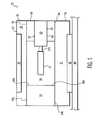
- FIG. 1schematically depicts electronic multisensor assembly 20 of one embodiment of the present invention.
- Assembly 20includes multiple sensor device 22 comprised of wafer members 30 , 40 , and 50 .
- wafer members 30 , 40 , and 50are each provided as a corresponding die formed by dividing a larger wafer in an earlier processing stage, as will be more fully described in connection with the flowchart of FIG. 3 hereinafter.
- Wafer members 30 , 40 , and 50each define a respective wafer or material layer 31 , 41 , and 51 of assembly 20 .
- Layer 51includes opposing sides 54 a and 54 b that are attached to layers 31 and 41 at boundaries 34 and 44 , respectively.
- Device 22is mounted to substrate 60 .
- Substrate 60is only partially shown in FIG. 1 .
- wafer members 30 , 40 , and 50 of device 22are each comprised of a standard semiconductor material.
- any of wafer members 30 , 40 , and/or 50can be comprised of a polymer, ceramic, and/or metal, to name just a few examples.
- the composition of wafer member 30 , 40 , and/or 50can otherwise vary as would occur to one skilled in the art.
- Wafer member 30includes finger print reader sensor 32
- wafer member 40includes a joystick movement sensor 42 .
- sensor 32is conveniently positioned for direct or indirect engagement with a finger to read a corresponding finger print due to its location opposite substrate 60 , while sensors 42 and 52 do not need to be positioned for such engagement.
- Wafer member 50includes a MEMS device in the form of electromechanical motion sensor 52 .
- sensor 52is in the form of accelerometer 55 .
- Accelerometer 55includes base portion 53 adjacent cavity 56 .
- Cavity 56extends through wafer member 50 defining aperture 56 a in side 54 a and aperture 56 b in side 54 b .
- Accelerometer 55further includes sensor member 57 in the form of mechanical arm 57 a coupled to base 53 .
- Mechanical arm 57 aextends from base 53 into cavity 56 , and is free to flex and/or otherwise move therein to electromechanically generate an electronic signal with sensor 52 corresponding to acceleration.
- sensor member 57is enclosed in cavity 56 by covering apertures 56 a and 56 b with wafer members 30 and 40 , respectively.
- Wafer members 30 and 40are joined to wafer member 50 to provide a hermetic seal that protects member 57 from damage by a source external to cavity 56 .
- wafer members 30 and 40provide a protective seal to reduce, if not eliminate, undesired exposure of internal workings.
- wafer members 30 and 40also include corresponding sensors 32 and 42 , the space occupied by the MEMS device (sensor 52 ) is vertically shared with sensors 32 and 42 .
- the resulting device 22 and assembly 20can be utilized in a manner that occupies less space compared to a configuration that as uses one or more of the sensors separately. It should be appreciated that in alternative embodiments, more or fewer sensors may be assembled together in accordance with the teachings of the present application.
- only one side 54 a or 54 b of wafer member 50includes an aperture exposing sensor 52 for which only one corresponding wafer member 30 or 40 may be attached to wafer member 50 to provide a protective enclosure.
- System 120includes handheld communication device 130 in the form of a mobile (or cellular) telephone 132 .
- Device 130includes multisensor assembly 20 and circuitry 122 .
- Circuitry 122is electrically coupled to multisensor assembly 20 .
- Circuitry 122is arranged to provide electrical power to sensor 32 , sensor 42 , and/or sensor 52 as needed or desired.
- circuitry 122is configured to receive detection signals from sensors 32 , 42 , and 52 ; and utilize such signals as desired in the operation of device 130 .
- sensor 32can be utilized as a security measure.
- a fingerprint identification signal determined via sensor 32is required to utilize some or all of the functionality of telephone 132 with or without other contingencies.
- sensor 42can be utilized to implement a joystick-controlled display pointer or cursor for telephone 132 (not shown) or the like.
- Sensor 52can be used for a location-reporting operation of telephone 132 .
- signals from sensor 52are used to augment a primary Geosynchronous Positioning Satellite (GPS) locating subsystem to accommodate poor GPS reception or the like.
- GPSGeosynchronous Positioning Satellite
- one or more of sensors 32 , 42 , and 52can be utilized in a different functional capacity for telephone 132 and/or may be of a different sensor type altogether.
- assembly 22is utilized in another device type, such as a Personal Digital Assistant (PDA), a personal computer (notebook, laptop, or otherwise), an electronic game device, an electronic operator control or input device, and/or such different device as would occur to one skilled in the art.
- PDAPersonal Digital Assistant
- a personal computernotebook, laptop, or otherwise
- an electronic game devicesuch as would occur to one skilled in the art.
- FIG. 3depicts manufacturing procedure 220 in flowchart form.
- Procedure 220is one mode of making a device that includes assembly 22 .
- Procedure 220starts with operation 222 .
- each wafer member 30 , 40 , and 50is processed to provide the corresponding sensor 32 , 42 , 52 that each carry.
- Each of wafer members 30 , 40 , 50is processed by standard techniques including selective doping, etching, metalization, and/or various lithographic or different fabrication techniques desired to provide the respective sensor 32 , 42 , and 52 .
- member 57 of wafer member 50is formed by standard etching techniques, which leaves cavity 56 surrounding it.
- each of wafer members 30 , 40 , and 50is provided as a wafer die that results from separating a larger corresponding wafer into a number of pieces (dice) or “chips.”
- each diecarries the same type of sensor 32 , 42 , or 52 .
- the larger wafercan provide multiple sensors of the same type and three different larger wafers can be used to respectively make several of each type of wafer member 30 , 40 , and 50 (and correspondingly sensors 32 , 42 , and 52 ).
- Procedure 220proceeds from operation 222 to operation 224 .
- wafer member 30 and wafer member 40 resulting from operation 222are attached on side 54 a and side 54 b of wafer member 50 , respectively.
- This attachment at boundary 34 and/or boundary 44can be by bonding with an adhesive or the like, fusing, and/or a different joining technique as would occur to one skilled in the art.
- operation 224results in a hermetic seal to protect accelerometer 55 —especially member 57 ; however, in other embodiments, the attachment need not provide such a seal.
- procedure 220continues with operation 226 .
- wafer member 40is mounted on substrate 60 using standard techniques.
- Substrate 60can be a semiconductor, metal, ceramic, a polymeric material and/or of a different composition as would occur to one skilled in the art. In still other embodiments, substrate 60 is absent.
- Procedure 220continues with operation 228 .
- assembly 20is electrically coupled to circuitry of which circuitry 122 is just one nonlimiting example.
- the resulting configurationis assembled into the application device in operation 230 .
- This devicemay be a handheld communication device 130 or such different device as would occur to one skilled in the art.
- the application deviceis operated. Operation 232 can be performed to test device functionality and/or as a consequence of using the device. It should be appreciated that procedure 220 is just one of many manufacturing processes for device 22 , multisensor assembly 20 , and systems including such items.
Landscapes
- Physics & Mathematics (AREA)
- General Physics & Mathematics (AREA)
- Engineering & Computer Science (AREA)
- Computer Hardware Design (AREA)
- Microelectronics & Electronic Packaging (AREA)
- Position Input By Displaying (AREA)
- Micromachines (AREA)
- Pressure Sensors (AREA)
- Image Input (AREA)
- Measuring Fluid Pressure (AREA)
- Control Of Motors That Do Not Use Commutators (AREA)
- Ultra Sonic Daignosis Equipment (AREA)
Abstract
Description
Claims (29)
Priority Applications (1)
| Application Number | Priority Date | Filing Date | Title |
|---|---|---|---|
| US11/721,029US8735198B2 (en) | 2004-12-06 | 2005-12-06 | Electromechanical sensor apparatus and methods with multisensing aspects |
Applications Claiming Priority (3)
| Application Number | Priority Date | Filing Date | Title |
|---|---|---|---|
| US63393204P | 2004-12-06 | 2004-12-06 | |
| PCT/IB2005/054085WO2006061781A1 (en) | 2004-12-06 | 2005-12-06 | Multisensor assembly |
| US11/721,029US8735198B2 (en) | 2004-12-06 | 2005-12-06 | Electromechanical sensor apparatus and methods with multisensing aspects |
Publications (2)
| Publication Number | Publication Date |
|---|---|
| US20090211359A1 US20090211359A1 (en) | 2009-08-27 |
| US8735198B2true US8735198B2 (en) | 2014-05-27 |
Family
ID=36050046
Family Applications (1)
| Application Number | Title | Priority Date | Filing Date |
|---|---|---|---|
| US11/721,029Active2030-02-05US8735198B2 (en) | 2004-12-06 | 2005-12-06 | Electromechanical sensor apparatus and methods with multisensing aspects |
Country Status (8)
| Country | Link |
|---|---|
| US (1) | US8735198B2 (en) |
| EP (1) | EP1828048B1 (en) |
| JP (1) | JP2008523466A (en) |
| KR (1) | KR20070093990A (en) |
| CN (1) | CN101115675B (en) |
| AT (1) | ATE470646T1 (en) |
| DE (1) | DE602005021818D1 (en) |
| WO (1) | WO2006061781A1 (en) |
Families Citing this family (6)
| Publication number | Priority date | Publication date | Assignee | Title |
|---|---|---|---|---|
| US9105751B2 (en) | 2011-11-11 | 2015-08-11 | International Business Machines Corporation | Integrated semiconductor devices with single crystalline beam, methods of manufacture and design structure |
| US8546240B2 (en) | 2011-11-11 | 2013-10-01 | International Business Machines Corporation | Methods of manufacturing integrated semiconductor devices with single crystalline beam |
| US8629036B2 (en) | 2011-11-11 | 2014-01-14 | International Business Machines Corporation | Integrated semiconductor devices with amorphous silicon beam, methods of manufacture and design structure |
| CN104649217B (en)* | 2014-12-23 | 2016-03-23 | 北京时代民芯科技有限公司 | A single-chip processing method for multiple MEMS sensors |
| CN104819730B (en)* | 2015-05-06 | 2017-12-05 | 歌尔股份有限公司 | A kind of MEMS inertial sensor and its manufacture method |
| WO2017093814A1 (en)* | 2015-12-04 | 2017-06-08 | Uti Limited Partnership | Wearable inertial electronic device |
Citations (7)
| Publication number | Priority date | Publication date | Assignee | Title |
|---|---|---|---|---|
| US6122964A (en)* | 1998-02-28 | 2000-09-26 | Robert Bosch Gmbh | Micromechanical comb structure |
| WO2001022351A1 (en) | 1999-09-17 | 2001-03-29 | Black Gerald R | Identity authentication system and method |
| WO2001022651A2 (en) | 1999-09-20 | 2001-03-29 | Ethentica, Inc. | Cryptographic server with provisions for interoperability between cryptographic systems |
| US6504385B2 (en) | 2001-05-31 | 2003-01-07 | Hewlett-Pakcard Company | Three-axis motion sensor |
| US6539101B1 (en)* | 1998-04-07 | 2003-03-25 | Gerald R. Black | Method for identity verification |
| US20030090737A1 (en) | 1999-05-25 | 2003-05-15 | Kia Silverbrook | Method and system for composition and delivery of electronic mail with coded marks |
| EP1460038A2 (en) | 2003-03-20 | 2004-09-22 | Robert Bosch Gmbh | Electromechanical system having a controlled atmosphere, and method of fabricating same |
- 2005
- 2005-12-06ATAT05823700Tpatent/ATE470646T1/ennot_activeIP Right Cessation
- 2005-12-06KRKR1020077015618Apatent/KR20070093990A/ennot_activeWithdrawn
- 2005-12-06DEDE602005021818Tpatent/DE602005021818D1/enactiveActive
- 2005-12-06CNCN2005800477876Apatent/CN101115675B/ennot_activeExpired - Fee Related
- 2005-12-06USUS11/721,029patent/US8735198B2/enactiveActive
- 2005-12-06JPJP2007543996Apatent/JP2008523466A/ennot_activeWithdrawn
- 2005-12-06WOPCT/IB2005/054085patent/WO2006061781A1/enactiveApplication Filing
- 2005-12-06EPEP05823700Apatent/EP1828048B1/ennot_activeNot-in-force
Patent Citations (9)
| Publication number | Priority date | Publication date | Assignee | Title |
|---|---|---|---|---|
| US6122964A (en)* | 1998-02-28 | 2000-09-26 | Robert Bosch Gmbh | Micromechanical comb structure |
| US6539101B1 (en)* | 1998-04-07 | 2003-03-25 | Gerald R. Black | Method for identity verification |
| US20030090737A1 (en) | 1999-05-25 | 2003-05-15 | Kia Silverbrook | Method and system for composition and delivery of electronic mail with coded marks |
| WO2001022351A1 (en) | 1999-09-17 | 2001-03-29 | Black Gerald R | Identity authentication system and method |
| WO2001022651A2 (en) | 1999-09-20 | 2001-03-29 | Ethentica, Inc. | Cryptographic server with provisions for interoperability between cryptographic systems |
| US6504385B2 (en) | 2001-05-31 | 2003-01-07 | Hewlett-Pakcard Company | Three-axis motion sensor |
| CN1389704A (en) | 2001-05-31 | 2003-01-08 | 惠普公司 | Three-shaft moving sensor |
| EP1460038A2 (en) | 2003-03-20 | 2004-09-22 | Robert Bosch Gmbh | Electromechanical system having a controlled atmosphere, and method of fabricating same |
| US20040183214A1 (en)* | 2003-03-20 | 2004-09-23 | Aaron Partridge | Electromechanical system having a controlled atmosphere, and method of fabricating same |
Also Published As
| Publication number | Publication date |
|---|---|
| JP2008523466A (en) | 2008-07-03 |
| ATE470646T1 (en) | 2010-06-15 |
| EP1828048A1 (en) | 2007-09-05 |
| CN101115675A (en) | 2008-01-30 |
| KR20070093990A (en) | 2007-09-19 |
| US20090211359A1 (en) | 2009-08-27 |
| DE602005021818D1 (en) | 2010-07-22 |
| WO2006061781A1 (en) | 2006-06-15 |
| EP1828048B1 (en) | 2010-06-09 |
| CN101115675B (en) | 2011-08-17 |
Similar Documents
| Publication | Publication Date | Title |
|---|---|---|
| US10508961B2 (en) | Semiconductor package with air pressure sensor | |
| US6891239B2 (en) | Integrated sensor and electronics package | |
| EP1214864B1 (en) | Silicon-based sensor system | |
| CN210030037U (en) | Semiconductor die and electronic system | |
| US20140090485A1 (en) | MEMS Pressure Sensor Assembly | |
| TWI730094B (en) | Piezoelectric package-integrated sensing devices | |
| WO2004071943A3 (en) | Electronic device and its manufacturing method device | |
| WO2011119317A1 (en) | Integrated multi-axis hybrid magnetic field sensor | |
| WO2006055731A1 (en) | Microelectromechanical systems contact stress sensor | |
| JP2008039664A (en) | Multirange acceleration sensor | |
| US8735198B2 (en) | Electromechanical sensor apparatus and methods with multisensing aspects | |
| US20040063239A1 (en) | Fabricating complex micro-electromechanical systems using an intermediate electrode layer | |
| US20150355220A1 (en) | Inertial sensor module having hermetic seal formed of metal and multi-axis sensor employing the same | |
| US7334491B2 (en) | Sensor arrangement, in particular a micro-mechanical sensor arrangement | |
| JP2008008672A (en) | Acceleration sensor | |
| JP5240657B2 (en) | Sensing element, sensing device, orientation detection device, and information device | |
| JP5221940B2 (en) | Semiconductor element mounting structure | |
| JP2007292692A (en) | Magnetic device | |
| TWI729021B (en) | Microelectronic devices for isolating drive and sense signals of sensing devices | |
| Gabriel | Akustica | |
| US20090095076A1 (en) | Acceleration Sensor Device and Sensor Apparatus | |
| CN101253411A (en) | Acceleration sensor device and sensor device | |
| KR100893755B1 (en) | Pointing device and electronic device having the same | |
| JP2006317184A (en) | Magnetic type acceleration sensor, and compact acceleration geomagnetism detector using same | |
| Ramesham | Assessment and Assurance of Microelectronics Packaging Technology of Microelectromechanical Systems (MEMS) |
Legal Events
| Date | Code | Title | Description |
|---|---|---|---|
| AS | Assignment | Owner name:NXP B.V., NETHERLANDS Free format text:ASSIGNMENT OF ASSIGNORS INTEREST;ASSIGNORS:O'MAHONY, PADRAIG;CARIS, FRANK;KERSJES, THEO;AND OTHERS;SIGNING DATES FROM 20090331 TO 20090430;REEL/FRAME:022644/0276 Owner name:NXP B.V., NETHERLANDS Free format text:ASSIGNMENT OF ASSIGNORS INTEREST;ASSIGNORS:O'MAHONY, PADRAIG;CARIS, FRANK;KERSJES, THEO;AND OTHERS;REEL/FRAME:022644/0276;SIGNING DATES FROM 20090331 TO 20090430 | |
| STCF | Information on status: patent grant | Free format text:PATENTED CASE | |
| AS | Assignment | Owner name:MORGAN STANLEY SENIOR FUNDING, INC., MARYLAND Free format text:SECURITY AGREEMENT SUPPLEMENT;ASSIGNOR:NXP B.V.;REEL/FRAME:038017/0058 Effective date:20160218 | |
| AS | Assignment | Owner name:MORGAN STANLEY SENIOR FUNDING, INC., MARYLAND Free format text:CORRECTIVE ASSIGNMENT TO CORRECT THE REMOVE APPLICATION 12092129 PREVIOUSLY RECORDED ON REEL 038017 FRAME 0058. ASSIGNOR(S) HEREBY CONFIRMS THE SECURITY AGREEMENT SUPPLEMENT;ASSIGNOR:NXP B.V.;REEL/FRAME:039361/0212 Effective date:20160218 | |
| AS | Assignment | Owner name:MORGAN STANLEY SENIOR FUNDING, INC., MARYLAND Free format text:CORRECTIVE ASSIGNMENT TO CORRECT THE REMOVE APPLICATION 12681366 PREVIOUSLY RECORDED ON REEL 038017 FRAME 0058. ASSIGNOR(S) HEREBY CONFIRMS THE SECURITY AGREEMENT SUPPLEMENT;ASSIGNOR:NXP B.V.;REEL/FRAME:042985/0001 Effective date:20160218 Owner name:MORGAN STANLEY SENIOR FUNDING, INC., MARYLAND Free format text:CORRECTIVE ASSIGNMENT TO CORRECT THE REMOVE APPLICATION 12681366 PREVIOUSLY RECORDED ON REEL 039361 FRAME 0212. ASSIGNOR(S) HEREBY CONFIRMS THE SECURITY AGREEMENT SUPPLEMENT;ASSIGNOR:NXP B.V.;REEL/FRAME:042762/0145 Effective date:20160218 | |
| MAFP | Maintenance fee payment | Free format text:PAYMENT OF MAINTENANCE FEE, 4TH YEAR, LARGE ENTITY (ORIGINAL EVENT CODE: M1551) Year of fee payment:4 | |
| AS | Assignment | Owner name:NXP B.V., NETHERLANDS Free format text:RELEASE BY SECURED PARTY;ASSIGNOR:MORGAN STANLEY SENIOR FUNDING, INC.;REEL/FRAME:050745/0001 Effective date:20190903 | |
| AS | Assignment | Owner name:MORGAN STANLEY SENIOR FUNDING, INC., MARYLAND Free format text:CORRECTIVE ASSIGNMENT TO CORRECT THE REMOVE APPLICATION 12298143 PREVIOUSLY RECORDED ON REEL 042985 FRAME 0001. ASSIGNOR(S) HEREBY CONFIRMS THE SECURITY AGREEMENT SUPPLEMENT;ASSIGNOR:NXP B.V.;REEL/FRAME:051029/0001 Effective date:20160218 Owner name:MORGAN STANLEY SENIOR FUNDING, INC., MARYLAND Free format text:CORRECTIVE ASSIGNMENT TO CORRECT THE REMOVE APPLICATION 12298143 PREVIOUSLY RECORDED ON REEL 042762 FRAME 0145. ASSIGNOR(S) HEREBY CONFIRMS THE SECURITY AGREEMENT SUPPLEMENT;ASSIGNOR:NXP B.V.;REEL/FRAME:051145/0184 Effective date:20160218 Owner name:MORGAN STANLEY SENIOR FUNDING, INC., MARYLAND Free format text:CORRECTIVE ASSIGNMENT TO CORRECT THE REMOVE APPLICATION 12298143 PREVIOUSLY RECORDED ON REEL 039361 FRAME 0212. ASSIGNOR(S) HEREBY CONFIRMS THE SECURITY AGREEMENT SUPPLEMENT;ASSIGNOR:NXP B.V.;REEL/FRAME:051029/0387 Effective date:20160218 Owner name:MORGAN STANLEY SENIOR FUNDING, INC., MARYLAND Free format text:CORRECTIVE ASSIGNMENT TO CORRECT THE REMOVE APPLICATION12298143 PREVIOUSLY RECORDED ON REEL 042762 FRAME 0145. ASSIGNOR(S) HEREBY CONFIRMS THE SECURITY AGREEMENT SUPPLEMENT;ASSIGNOR:NXP B.V.;REEL/FRAME:051145/0184 Effective date:20160218 Owner name:MORGAN STANLEY SENIOR FUNDING, INC., MARYLAND Free format text:CORRECTIVE ASSIGNMENT TO CORRECT THE REMOVE APPLICATION 12298143 PREVIOUSLY RECORDED ON REEL 038017 FRAME 0058. ASSIGNOR(S) HEREBY CONFIRMS THE SECURITY AGREEMENT SUPPLEMENT;ASSIGNOR:NXP B.V.;REEL/FRAME:051030/0001 Effective date:20160218 Owner name:MORGAN STANLEY SENIOR FUNDING, INC., MARYLAND Free format text:CORRECTIVE ASSIGNMENT TO CORRECT THE REMOVE APPLICATION12298143 PREVIOUSLY RECORDED ON REEL 039361 FRAME 0212. ASSIGNOR(S) HEREBY CONFIRMS THE SECURITY AGREEMENT SUPPLEMENT;ASSIGNOR:NXP B.V.;REEL/FRAME:051029/0387 Effective date:20160218 Owner name:MORGAN STANLEY SENIOR FUNDING, INC., MARYLAND Free format text:CORRECTIVE ASSIGNMENT TO CORRECT THE REMOVE APPLICATION12298143 PREVIOUSLY RECORDED ON REEL 042985 FRAME 0001. ASSIGNOR(S) HEREBY CONFIRMS THE SECURITY AGREEMENT SUPPLEMENT;ASSIGNOR:NXP B.V.;REEL/FRAME:051029/0001 Effective date:20160218 | |
| MAFP | Maintenance fee payment | Free format text:PAYMENT OF MAINTENANCE FEE, 8TH YEAR, LARGE ENTITY (ORIGINAL EVENT CODE: M1552); ENTITY STATUS OF PATENT OWNER: LARGE ENTITY Year of fee payment:8 | |
| MAFP | Maintenance fee payment | Free format text:PAYMENT OF MAINTENANCE FEE, 12TH YEAR, LARGE ENTITY (ORIGINAL EVENT CODE: M1553); ENTITY STATUS OF PATENT OWNER: LARGE ENTITY Year of fee payment:12 |