US8732646B2 - PLD architecture for flexible placement of IP function blocks - Google Patents
PLD architecture for flexible placement of IP function blocksDownload PDFInfo
- Publication number
- US8732646B2 US8732646B2US13/847,666US201313847666AUS8732646B2US 8732646 B2US8732646 B2US 8732646B2US 201313847666 AUS201313847666 AUS 201313847666AUS 8732646 B2US8732646 B2US 8732646B2
- Authority
- US
- United States
- Prior art keywords
- routing
- array
- function block
- interface region
- lines
- Prior art date
- Legal status (The legal status is an assumption and is not a legal conclusion. Google has not performed a legal analysis and makes no representation as to the accuracy of the status listed.)
- Expired - Fee Related
Links
- 239000004065semiconductorSubstances0.000claims9
- 230000008878couplingEffects0.000claims3
- 238000010168coupling processMethods0.000claims3
- 238000005859coupling reactionMethods0.000claims3
- 230000006870functionEffects0.000description51
- 235000012489doughnutsNutrition0.000description4
- 239000002184metalSubstances0.000description3
- 230000004048modificationEffects0.000description3
- 238000012986modificationMethods0.000description3
- 230000015556catabolic processEffects0.000description2
- 238000006731degradation reactionMethods0.000description2
- 238000000034methodMethods0.000description2
- 230000006978adaptationEffects0.000description1
- 230000004075alterationEffects0.000description1
- 238000003491arrayMethods0.000description1
- 238000004891communicationMethods0.000description1
Images


Classifications
- H—ELECTRICITY
- H03—ELECTRONIC CIRCUITRY
- H03K—PULSE TECHNIQUE
- H03K19/00—Logic circuits, i.e. having at least two inputs acting on one output; Inverting circuits
- H03K19/02—Logic circuits, i.e. having at least two inputs acting on one output; Inverting circuits using specified components
- H03K19/173—Logic circuits, i.e. having at least two inputs acting on one output; Inverting circuits using specified components using elementary logic circuits as components
- H03K19/177—Logic circuits, i.e. having at least two inputs acting on one output; Inverting circuits using specified components using elementary logic circuits as components arranged in matrix form
- H03K19/17736—Structural details of routing resources
- H—ELECTRICITY
- H03—ELECTRONIC CIRCUITRY
- H03K—PULSE TECHNIQUE
- H03K19/00—Logic circuits, i.e. having at least two inputs acting on one output; Inverting circuits
- H03K19/02—Logic circuits, i.e. having at least two inputs acting on one output; Inverting circuits using specified components
- H03K19/173—Logic circuits, i.e. having at least two inputs acting on one output; Inverting circuits using specified components using elementary logic circuits as components
- H03K19/177—Logic circuits, i.e. having at least two inputs acting on one output; Inverting circuits using specified components using elementary logic circuits as components arranged in matrix form
- H03K19/17724—Structural details of logic blocks
- H03K19/17732—Macroblocks
- H—ELECTRICITY
- H03—ELECTRONIC CIRCUITRY
- H03K—PULSE TECHNIQUE
- H03K19/00—Logic circuits, i.e. having at least two inputs acting on one output; Inverting circuits
- H03K19/02—Logic circuits, i.e. having at least two inputs acting on one output; Inverting circuits using specified components
- H03K19/173—Logic circuits, i.e. having at least two inputs acting on one output; Inverting circuits using specified components using elementary logic circuits as components
- H03K19/177—Logic circuits, i.e. having at least two inputs acting on one output; Inverting circuits using specified components using elementary logic circuits as components arranged in matrix form
- H03K19/1778—Structural details for adapting physical parameters
- H03K19/17796—Structural details for adapting physical parameters for physical disposition of blocks
Definitions
- the present inventionis in the field of programmable logic devices (PLD's) and, more particularly, relates to a flexible architecture by which logic elements (LE's) of a PLD having an array of logic elements are replaced with intellectual property (IP) function blocks.
- PLD'sprogrammable logic devices
- LE'slogic elements
- IPintellectual property
- PLD'sprogrammable logic devices
- LE'slogic elements
- the base signal routing architecture between LE'sis designed such that LE-to-LE routing (typically performed by software programs that convert hardware design language program instructions into such routing) is optimized.
- Examples of PLD's having more than one arrayinclude PLD's in the APEX family of devices, by Altera Corporation of San Jose, Calif. It is sometimes desired to add one or more IP function blocks among an LE array.
- an LEis considered to be a basic—or most common—logic element that functions, for example, with respect to look-up table or macrocell logic.
- the LE's of an arrayare nominally connected by a base signal routing architecture.
- An IP function blockis a functional block that is not constrained by the function of the most common logic element.
- an IP function blockmay be a high-speed serial interface (HSSI), a digital signal processor or other microprocessor, ALU, memory, or a multiplier.
- IP function blockwhen an IP function block is added to an LE array, the IP function block is placed at an edge of the LE array and spanning the entire edge of the LE array. This minimizes the disruption in the base routing. Furthermore, by placing the IP function block at an edge of the array, the performance degradation that would otherwise be caused by routing over the IP function block is minimized.
- a disadvantage of placing the IP function block at an edge of the LE arrayis that the input/output (I/O) cells (for communication off the LE array) are conventionally located at the edge of the LE array.
- the IP function blockmay not even require access to the I/O cells at that edge but, nonetheless, impedes access by other elements (LE's, or even other IP function block) to the I/O cells at the edge where the IP function block is placed.
- a blocksuch as an embedded array block (EAB) completely replaces a logic array block (LAB) of LE's.
- EABembedded array block
- LABlogic array block
- IP function block placement within an LE array of a PLDhas commonly been an afterthought such that, typically, an IP function block was merely placed where it could best fit to minimize the disruption to the base signal routing architecture.
- a PLD architectureby which the placement of an IP function block is not dictated by the goal of minimizing the disruption to the base signal routing architecture.
- a “hole”is formed within an LE array of a PLD by interrupting the base signal routing architecture such that a hole is left for the IP function block to be incorporated.
- An interface regionis provided for interfacing the remaining base signal routing to the IP function block. This provides for flexible placement of IP function block within the regular LE-routing structure of the PLD.
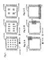
- FIG. 1illustrates possible placements of “big” IP function blocks within a PLD and not adjacent to an edge of the LE array, for a “big” IP function block such as a memory for which direct I/O access is not a requirement.
- FIGS. 2A , 2 B and 2 Cillustrate possible placements of big IP function blocks within a PLD and adjacent to an edge of the LE array such that direct I/O access is provided.
- FIG. 3illustrates a “donut hole” within the context of a PLD, for placement of a “big” IP function block within a PLD and not adjacent to an edge of the LE array.
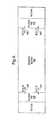
- FIG. 4illustrates, in greater detail, a “big block” interface region as used in FIGS. 1 , 2 and 3 .
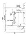
- FIG. 5illustrates the horizontal interface to a “big block” that is a large random access memory (“MRAM”).
- MRAMlarge random access memory
- FIG. 6illustrates the vertical interface to the MRAM.
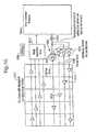
- FIG. 7is a table illustrating connectivity details of the MRAM_LIM
- FIG. 8is a table illustrating the MegaRAM_Out signal connections.
- FIG. 9is a table illustrating the Mega-RAM interface specifications.
- FIG. 10illustrates an embodiment of a staggered routing architecture, in which the partial lines at the boundary of the staggered routing architecture are driven.
- FIGS. 1 and 2illustrate possible floorplans for a PLD architecture in accordance with an aspect of the invention.
- the illustrations in FIG. 1are examples only, and the invention is not limited to the examples shown in FIG. 1 .
- a method of creating the FIG. 1 floorplans(and other floorplans within the scope of the invention) is now described.
- the base signal routing architectureis defined and optimized for LE's. For example, an array of LE's is created for a particular target die size. For variants of the created LE array, as discussed in the Background, it is desired to place the IP function block within the LE array. In some embodiments, the IP function block is added as IP function blocks at some desired uniform density, although the density of IP function blocks need not be uniform. For IP function blocks added to the LE array, LE's are replaced. Thus, there is a tradeoff between LE's and the amount of IP added to the die.
- the array of LE's for which a particular base signal routing architecture is optimizedmay occupy substantially an entire target die. Alternately, a base signal routing architecture may be optimized for an array of LE's that coexists on a die with other circuitry, including other LE's.
- FIGS. 1A , 1 B and 1 Cillustrate IP function block 110 incorporated within the interior of an LE array, for an IP function block that does not require direct I/O pad 112 access.
- FIGS. 2A and 2Billustrate an IP function block 120 incorporated at the edge of the LE array but not spanning the entire edge of the LE array, such that I/O pad 112 access is provided to the IP function block 120 .
- the IP function blockcan even displace I/O pads 112 , if desired.
- FIG. 3illustrates how an IP function block is incorporated as a “donut hole” 302 as applied to the FIG. 1 examples. That is, within the region where the IP function block is incorporated, the base signal routing architecture is interrupted, and a hole 302 is left (at least in one layer of the metal) for the IP function block to be incorporated. In addition, an interface region 304 is provided completely surrounding the hole 302 for interfacing the remaining base signal array routing to the IP function block. A very specific example of one such interface block is described later with reference to FIGS. 5 and 6 .
- some of the lines of the base signal routing architecturemay be routed around the hole 302 by being raised from the interface region 304 at one side of the hole 302 to a different layer of the metal not occupied by the hole 302 and lowered back into the interface region 304 at another side of the hole 302 , typically the opposite side of the hole 302 .
- signal routing lines for driving shorter distancesare terminated, and routing lines for driving longer distances are raised to a different layer of metal, buffered across the hole, and lowered into the interface region at the opposite side of the donut hole.
- An interface regionis provided even when the IP function block is not to be bordered on all four sides by the base signal routing architecture as illustrated in the FIG. 3 embodiment but, rather, is to be bordered on two sides (an example of which is shown in FIG. 2A ), three sides (an example of which is shown in FIG. 2B ), or even one side (an example of which is shown in FIG. 2C ).
- the interface regionis typically provided on each side of the hole that borders the base signal routing architecture.
- FIG. 4illustrates an embodiment of the interface region 304 . That is, in accordance with the FIG. 4 , it is shown that, for some level of granularity, the interface region 408 includes up to 24 signal lines into the hole 402 and up to 12 signal lines out of the hole 402 .
- the interface region 408is built modularly, at a particular level of granularity. In one embodiment, the particular level of granularity is one width or height of the logic array block (LAB) of the LE array.
- LABlogic array block
- a design consideration for the placement of a holeis the number of signal lines in and out of a hole that would result from a particular placement, primarily as a result of the extent to which the hole would border the base signal routing architecture. This can be seen with reference again to FIGS. 2A and 2B .
- FIGS. 5 and 6illustrate a situation where the IP function block is a RAM block (designated in FIGS. 5 and 6 as a “Mega-RAM” 502 ).
- FIG. 5illustrates the situation from the horizontal routing perspective
- FIG. 6illustrates the situation from the vertical routing perspective.
- the Mega-RAM block 502spans multiple columns and multiple rows of the LE array, and therefore interfaces with many lines (“channels”) of routing.
- the general routingdoes not cross the Mega-RAM 502 . Rather, the general routing “dead ends” at the Mega-RAM Interface (a specific instance of the FIG. 3 interface region) to form the donut hole for the Mega-RAM.
- the H24 ( FIG. 5 ) and V16 ( FIG. 6 ) routing linesare buffered across the Mega-RAM block.
- the Mega-RAM horizontal interface 504( FIG. 5 ) allows the Mega-RAM to interface to logic to the left or to the right of the Mega-RAM.
- the Mega-RAM vertical interface 604( FIG. 6 ) allows the Mega-RAM to interface to logic above and below the Mega-RAM.
- the Mega-RAM vertical interface( FIG. 6 ) there are two groups of fifteen MRAM_LIM's (Not all are shown). Each of the two groups is fed by a different V-Channel.
- One Mega-RAM interfaceis provided on each of the left and right hand edges of the MegaRAM for every LAB row it spans, and one Mega-RAM interface is provided on each of the top and bottom edges of the Mega-Ram for every pair of LAB columns it spans.
- H and V routing lines in a typical embodimentconnect into MRAM_LIM's 506 , 606 a and 606 b (LAB input multiplexers).
- the MRAM_LIM 506 , 606 a and 606 bis a two stage 4-way sharing multiplexer.
- the routingis unidirectional (i.e., each line can carry a signal in one direction), then routing able to carry signals away from the MRAM will not be coupled to the input interface.
- bi-directional linesare used in addition to, or in place of, unidirectional lines.
- FIG. 7lists the number of “ways in per line” and the number of “connections per MRAM_LIM” for each of the Horizontal MegaRAM interface ( FIG. 5 ) and the Vertical MegaRAM interface ( FIG. 6 ). At the bottom of the FIG. 7 table, the listed totals include the total number of MRAM_LIM fan in signals, and the total number of MRAM_LIM multiplexers, for each of the Horizontal MegaRAM interface and the Vertical MegaRAM interface.
- Clock inputs 524are taken into the Mega-RAM block 502 from the global clock network at the side of the Mega-RAM block 502 through the Mega-RAM horizontal interface 504 in ( FIG. 5 ).
- the MRAM_CLOCK MUX 526chooses one of the eight LABCLK's that are feeding through the adjacent LABs. There is one clock input to the Mega-RAM 502 per row, although the Mega-RAM 502 typically would not use every clock input available to it.
- the Mega-RAM input mux(“MRIM”) is a fully populated 4-way mux-sharing mux that connects thirty LAB lines onto twenty-four I/O block inputs.
- the Mega-RAM interfaceuses the full-length and partial length (i.e., length four and length eight lines, in this embodiment) to connect to the core via the MRAM_DIM.
- the Mega-RAM interfaceprovides similar resources as are provided for a LAB to drive onto the core routing. For example, H4 lines extending four LAB's into the core are driven, and H4 lines extending three LAB's in or less are not driven. These partial length lines are driven to Vcc. In another embodiment, the partial length lines connect to the MRAM_LIM's as described below with reference to FIG. 10 .
- the Mega-RAM horizontal interfacecan also drive signals out onto the adjacent V-channel routing.
- Ten partial length sneak paths(H4, H8, V16, H24) (e.g., as collectively designated by line 528 ) are driven directly into adjacent LAB's by ten of the twelve MegaRAM_Out signals for a “quick” path to logic.
- Each MRAM driver input multiplexer (“MRAM DIM”) 612 a , 612 bsupports the V-channel at the edge of the core and the half H-channel able to carry signals from the MRAM in the direction of the core.
- the Mega-RAM vertical interface 604drives the full-length routing resources of two full V-channels. These drivers are dedicated to the MegaRAM_Out signals and do not support turns from other routing resources.
- the DIM's 612 a and 612 b associated with the V-line drivers in the Mega-RAM vertical interface 604are used to choose between MegaRAM_Out signals.
- Each DIM 612 a , 612 b in the vertical interfaceis a 4:1 mux that can be implemented in one or more stages, and each input to the DIM is a MegaRAM_Out signal.
- the connection pattern from the MegaRAM_Out signals to the DIM 612 a , 612 bis typically spread equally between the two V-channels.
- FIG. 9is a summary of the Mega_RAM interface specifications for each of the Mega_RAM Horizontal Interface and the Mega_RAM Vertical Interface, and lists the total number of the various interface components described above.
- the IP function blockmay be of two types—small and large.
- the terms small and large as used herecan be thought of as indicating size.
- One actual design consideration, however, in determining whether to consider particular IP function block as small or largeis a consideration of how much disruption to the timing of signal routing is to be tolerated.
- a small blockis an IP function block whose layout can be drawn at a width on the order of an LE width.
- the width of small blocksmay be wider than an LE so long as the timing of signal routing over the block does not get significantly larger than for routing over an LE.
- small blocksinclude MEAB's (medium sized embedded array blocks), SEAB's (small sized embedded array blocks) and a DSP block.
- large blocksare IP function blocks that typically have dimensions much larger than that of an LE. Extending the base signal routing architecture across these blocks without modification would cause routing over these blocks to be significantly larger than routing over an LE, forming a boundary in the PLD timing model.
- Such large blocksmay be inserted into the LE array as holes in the base signal routing architecture, as described above. In some sense, what occurs at the boundary between the base signal routing architecture and a hole is similar to the base signal routing architecture ending at the edge of an LE array.
- the LE routing linesare part of a staggered, uni-directional routing architecture.
- routing drivers 1006are included in the interface region 1008 (whether the I/O interface region or the hole interface region) to drive both the full and partial lines.
- the output ports 1010 of the logic block 1004connect to the drivers of both the “full” lines and the “partial” lines.
- Signal selection muxesmay be used in front of the drivers to add routing flexibility. As described above, the routing may also be implemented with segmented bi-directional lines.
- the partial lines 1002 driving out of the PLD core 1001feed an input selection mux 1012 to drive into the logic block 1004 .
- These partial lines 1002impose a smaller load on the drivers 1014 than do full lines 1016 , and having a small load makes the partial line 1002 a faster path into the PLD core 1001 . If area is a concern, drivers 1018 for partial lines 1002 may be smaller than drivers 1020 for full lines 1016 , and still not be at a speed disadvantage due to the smaller load.
- additional routing flexibilityis provided for signals from the PLD core 1001 to the PLD boundaries. Allowing the partial lines 1002 headed out of the PLD 1001 to drive into an IP function block 1004 increases the routability from the PLD core 1001 to the logic block 1004 .
- the additional drivers 1018may be used to provide the core 1001 access to more signals, or the signals may be used to provide more paths into the PLD core 1001 for a given signal. Thus, quite simply, lines that would have otherwise been unused are utilized to provide needed access to the PLD core 1001 .
Landscapes
- Physics & Mathematics (AREA)
- Mathematical Physics (AREA)
- Engineering & Computer Science (AREA)
- Computer Hardware Design (AREA)
- Computing Systems (AREA)
- General Engineering & Computer Science (AREA)
- Computer Networks & Wireless Communication (AREA)
- Design And Manufacture Of Integrated Circuits (AREA)
- Logic Circuits (AREA)
Abstract
Description
This application is a continuation of copending, commonly assigned U.S. patent application Ser. No. 13/468,928, filed May 10, 2012 (allowed), which is a continuation of U.S. patent application Ser. No. 12/465,464, filed May 13, 2009, now U.S. Pat. No. 8,201,129, which is a division of U.S. patent application Ser. No. 11/202,616, filed Aug. 12, 2005, now U.S. Pat. No. 7,584,447, which is a continuation of application Ser. No. 10/460,685, filed Jun. 11, 2003, now U.S. Pat. No. 7,058,920, which is a division of application Ser. No. 10/057,442, filed Jan. 25, 2002, now U.S. Pat. No. 6,605,962, which claims the benefit of U.S. Provisional Patent Application No. 60/289,311, filed May 6, 2001 (now expired), each of which is hereby incorporated by reference herein in its respective entirety.
The present invention is in the field of programmable logic devices (PLD's) and, more particularly, relates to a flexible architecture by which logic elements (LE's) of a PLD having an array of logic elements are replaced with intellectual property (IP) function blocks.
Conventional programmable logic devices (PLD's) comprise one or more arrays of logic elements (LE's), and the base signal routing architecture between LE's is designed such that LE-to-LE routing (typically performed by software programs that convert hardware design language program instructions into such routing) is optimized. Examples of PLD's having more than one array include PLD's in the APEX family of devices, by Altera Corporation of San Jose, Calif. It is sometimes desired to add one or more IP function blocks among an LE array. For the purposes of this disclosure, an LE is considered to be a basic—or most common—logic element that functions, for example, with respect to look-up table or macrocell logic. The LE's of an array are nominally connected by a base signal routing architecture. An IP function block is a functional block that is not constrained by the function of the most common logic element. For example, by way of illustration and not by limitation, an IP function block may be a high-speed serial interface (HSSI), a digital signal processor or other microprocessor, ALU, memory, or a multiplier.
Conventionally, when an IP function block is added to an LE array, the IP function block is placed at an edge of the LE array and spanning the entire edge of the LE array. This minimizes the disruption in the base routing. Furthermore, by placing the IP function block at an edge of the array, the performance degradation that would otherwise be caused by routing over the IP function block is minimized. A disadvantage of placing the IP function block at an edge of the LE array, however, is that the input/output (I/O) cells (for communication off the LE array) are conventionally located at the edge of the LE array. The IP function block may not even require access to the I/O cells at that edge but, nonetheless, impedes access by other elements (LE's, or even other IP function block) to the I/O cells at the edge where the IP function block is placed. In some cases, such as is described in U.S. Pat. No. 5,550,782, a block such as an embedded array block (EAB) completely replaces a logic array block (LAB) of LE's. In this case, the routing connects to the EAB in much the same way that the routing interfaces with the conventional logic block and, thus, there is no corresponding performance degradation.
Clearly, placement of an IP function block within an LE array of a PLD has commonly been an afterthought such that, typically, an IP function block was merely placed where it could best fit to minimize the disruption to the base signal routing architecture. What is desired is a PLD architecture by which the placement of an IP function block is not dictated by the goal of minimizing the disruption to the base signal routing architecture.
In accordance with one aspect of the invention, a “hole” is formed within an LE array of a PLD by interrupting the base signal routing architecture such that a hole is left for the IP function block to be incorporated. An interface region is provided for interfacing the remaining base signal routing to the IP function block. This provides for flexible placement of IP function block within the regular LE-routing structure of the PLD.
The base signal routing architecture is defined and optimized for LE's. For example, an array of LE's is created for a particular target die size. For variants of the created LE array, as discussed in the Background, it is desired to place the IP function block within the LE array. In some embodiments, the IP function block is added as IP function blocks at some desired uniform density, although the density of IP function blocks need not be uniform. For IP function blocks added to the LE array, LE's are replaced. Thus, there is a tradeoff between LE's and the amount of IP added to the die. The array of LE's for which a particular base signal routing architecture is optimized may occupy substantially an entire target die. Alternately, a base signal routing architecture may be optimized for an array of LE's that coexists on a die with other circuitry, including other LE's.
An interface region is provided even when the IP function block is not to be bordered on all four sides by the base signal routing architecture as illustrated in theFIG. 3 embodiment but, rather, is to be bordered on two sides (an example of which is shown inFIG. 2A ), three sides (an example of which is shown inFIG. 2B ), or even one side (an example of which is shown inFIG. 2C ). The interface region is typically provided on each side of the hole that borders the base signal routing architecture.
A design consideration for the placement of a hole is the number of signal lines in and out of a hole that would result from a particular placement, primarily as a result of the extent to which the hole would border the base signal routing architecture. This can be seen with reference again toFIGS. 2A and 2B .
Driving into theMega-RAM 502 is now described. H and V routing lines in a typical embodiment connect into MRAM_LIM's506,606aand606b(LAB input multiplexers). TheMRAM_LIM
Connectivity details of theMRAM_LIM FIG. 7 . Briefly,FIG. 7 lists the number of “ways in per line” and the number of “connections per MRAM_LIM” for each of the Horizontal MegaRAM interface (FIG. 5 ) and the Vertical MegaRAM interface (FIG. 6 ). At the bottom of theFIG. 7 table, the listed totals include the total number of MRAM_LIM fan in signals, and the total number of MRAM_LIM multiplexers, for each of the Horizontal MegaRAM interface and the Vertical MegaRAM interface.
Clock inputs524 are taken into theMega-RAM block 502 from the global clock network at the side of theMega-RAM block 502 through the Mega-RAMhorizontal interface 504 in (FIG. 5 ). TheMRAM_CLOCK MUX 526 chooses one of the eight LABCLK's that are feeding through the adjacent LABs. There is one clock input to the Mega-RAM502 per row, although the Mega-RAM502 typically would not use every clock input available to it.
The Mega-RAM input mux (“MRIM”) is a fully populated 4-way mux-sharing mux that connects thirty LAB lines onto twenty-four I/O block inputs.
Driving out of theMega-RAM 502 is now described. At the edge of the Mega-RAM, routing lines driving into the core do not have LAB's to drive them and are left as partial length lines. The Mega-RAM interface uses the full-length and partial length (i.e., length four and length eight lines, in this embodiment) to connect to the core via the MRAM_DIM. The Mega-RAM interface provides similar resources as are provided for a LAB to drive onto the core routing. For example, H4 lines extending four LAB's into the core are driven, and H4 lines extending three LAB's in or less are not driven. These partial length lines are driven to Vcc. In another embodiment, the partial length lines connect to the MRAM_LIM's as described below with reference toFIG. 10 .
The Mega-RAM horizontal interface can also drive signals out onto the adjacent V-channel routing. Ten partial length sneak paths (H4, H8, V16, H24) (e.g., as collectively designated by line528) are driven directly into adjacent LAB's by ten of the twelve MegaRAM_Out signals for a “quick” path to logic.
Each MRAM driver input multiplexer (“MRAM DIM”)612a,612bsupports the V-channel at the edge of the core and the half H-channel able to carry signals from the MRAM in the direction of the core. The Mega-RAMvertical interface 604 drives the full-length routing resources of two full V-channels. These drivers are dedicated to the MegaRAM_Out signals and do not support turns from other routing resources. The DIM's612aand612bassociated with the V-line drivers in the Mega-RAMvertical interface 604 are used to choose between MegaRAM_Out signals. EachDIM DIM
The number of MegaRAM_Out signal connections per DIM for each of the Mega_RAM Horizontal Interface (FIG. 5 ) and the Mega_RAM Vertical Interface (FIG. 6 ) are set forth inFIG. 8 .FIG. 9 is a summary of the Mega_RAM interface specifications for each of the Mega_RAM Horizontal Interface and the Mega_RAM Vertical Interface, and lists the total number of the various interface components described above.
It is noted that, typically, not all IP function blocks need be incorporated into an LE array using the hole concept. For example, the IP function block may be of two types—small and large. In general, the terms small and large as used here can be thought of as indicating size. One actual design consideration, however, in determining whether to consider particular IP function block as small or large is a consideration of how much disruption to the timing of signal routing is to be tolerated. For example, in accordance with one embodiment, a small block is an IP function block whose layout can be drawn at a width on the order of an LE width. In accordance with this embodiment, the width of small blocks may be wider than an LE so long as the timing of signal routing over the block does not get significantly larger than for routing over an LE. For example, in one 0.13 μm architecture, it has been deemed that the timing of the signal routing over a block of roughly 5 LE widths does not get significantly larger than for routing over an LE. Typically, additional inputs and/or outputs may be added that exceed the width of an LE, so long as the base signal routing architecture across the IP function block is maintained with the LE's surrounding the small block. Another consideration for determining whether an IP function block is large (implemented using the hole concept) or small is the size of the IP function block relative to the overhead associated with employing an interface region. In one embodiment, small blocks include MEAB's (medium sized embedded array blocks), SEAB's (small sized embedded array blocks) and a DSP block. By contrast, large blocks are IP function blocks that typically have dimensions much larger than that of an LE. Extending the base signal routing architecture across these blocks without modification would cause routing over these blocks to be significantly larger than routing over an LE, forming a boundary in the PLD timing model. Such large blocks may be inserted into the LE array as holes in the base signal routing architecture, as described above. In some sense, what occurs at the boundary between the base signal routing architecture and a hole is similar to the base signal routing architecture ending at the edge of an LE array.
In some embodiments, shown with reference toFIG. 10 , the LE routing lines are part of a staggered, uni-directional routing architecture. As a result of the staggering, as can be seen fromFIG. 10 , there arepartial lines 1002 at boundaries formed by, for example, the I/O interface 1008 at the edge of thePLD 1001 or by an inserted IP function block (designated by reference numeral1004). In accordance with some such staggered architecture embodiments, routingdrivers 1006 are included in the interface region1008 (whether the I/O interface region or the hole interface region) to drive both the full and partial lines. Theoutput ports 1010 of thelogic block 1004 connect to the drivers of both the “full” lines and the “partial” lines. Signal selection muxes may be used in front of the drivers to add routing flexibility. As described above, the routing may also be implemented with segmented bi-directional lines.
Thepartial lines 1002 driving out of thePLD core 1001 feed aninput selection mux 1012 to drive into thelogic block 1004. Thesepartial lines 1002 impose a smaller load on thedrivers 1014 than dofull lines 1016, and having a small load makes the partial line1002 a faster path into thePLD core 1001. If area is a concern,drivers 1018 forpartial lines 1002 may be smaller thandrivers 1020 forfull lines 1016, and still not be at a speed disadvantage due to the smaller load.
Furthermore, by driving even thepartial lines 1002, additional routing flexibility is provided for signals from thePLD core 1001 to the PLD boundaries. Allowing thepartial lines 1002 headed out of thePLD 1001 to drive into anIP function block 1004 increases the routability from thePLD core 1001 to thelogic block 1004. In addition, theadditional drivers 1018 may be used to provide thecore 1001 access to more signals, or the signals may be used to provide more paths into thePLD core 1001 for a given signal. Thus, quite simply, lines that would have otherwise been unused are utilized to provide needed access to thePLD core 1001.
While the present invention has been particularly described with respect to the illustrated embodiments, it will be appreciated that various alterations, modifications and adaptations may be based on the present disclosure, and are intended to be within the scope of the present invention. While the invention has been described in connection with what are presently considered to be the most practical and preferred embodiments, it is to be understood that the present invention is not limited to the disclosed embodiment but, on the contrary, is intended to cover various modifications and equivalent arrangements included within the scope of the claims. For example, the techniques described herein may be applied to other types of fixed blocks or routing structures.
Claims (20)
1. A programmable logic device comprising:
an interface region for interconnecting an IP function block and a logic element (LE) array, the interface region comprising routing circuitry for transmitting signals from the IP function block to the LE array, wherein the routing circuitry comprises:
partial routing lines driven to a reference voltage, wherein the partial routing lines end at an edge of the interface region, and
full routing lines driven by a routing driver, wherein the full routing lines extend into the LE array.
2. The programmable logic device ofclaim 1 , wherein the routing circuitry is a first routing circuitry, and wherein the interface region further comprises a second routing circuitry for transmitting signals from the LE array to the IP function block, and wherein the second routing circuitry comprises:
an input multiplexer for selectively coupling input signals from the LE array to the IP function block.
3. The programmable logic device ofclaim 2 , wherein the first routing circuitry and the second routing circuitry comprise unidirectional routing lines.
4. The programmable logic device ofclaim 2 , wherein the second routing circuitry further comprises a first set of routing drivers for routing the full routing lines and a second set of routing drivers for routing the partial routing lines, and wherein routing drivers in the second set of routing drivers are smaller than routing drivers in the first set of routing drivers.
5. The programmable logic device ofclaim 1 , wherein the IP function block spans a plurality of rows of the LE array, and wherein the interface region has a granularity substantially similar to a width of a logic array block (LAB) of the LE array.
6. The programmable logic device ofclaim 1 , wherein the interface region further comprises:
a first subset of routing lines terminating at the interface region to form a hole for the IP function block; and
a second subset of routing lines buffered across the IP function block to couple a LAB on a first side of the IP function block to a LAB on a second side of the IP function block.
7. The programmable logic device ofclaim 1 , wherein the interface region provides, to the IP function block, a clock signal input per row of the LE array spanned by the IP function block.
8. A semiconductor integrated circuit, comprising:
an interface region comprising routing circuitry for transmitting signals from an IP function block to a logic element (LE) array, wherein the routing circuitry comprises:
partial routing lines driven to a reference voltage, wherein the partial routing lines end at an edge of the interface region, and
full routing lines driven by respective routing drivers, wherein the full routing lines extend into the LE array.
9. The semiconductor integrated circuit ofclaim 8 , wherein the routing circuitry is a first routing circuitry, and wherein the interface region further comprises a second routing circuitry for transmitting signals from the LE array to the IP function block, and wherein the second routing circuitry comprises:
an input multiplexer for selectively coupling input signals from the LE array to the IP function block.
10. The semiconductor integrated circuit ofclaim 9 , wherein the first routing circuitry and the second routing circuitry comprise unidirectional routing lines.
11. The semiconductor integrated circuit ofclaim 9 , wherein the second routing circuitry further comprises a first set of routing drivers for routing the full routing lines and a second set of routing drivers for routing the partial routing lines, and wherein routing drivers in the second set of routing drivers are smaller than routing drivers in the first set of routing drivers.
12. The semiconductor integrated circuit ofclaim 8 , wherein the IP function block spans a plurality of rows of the LE array, and wherein the interface region has a granularity substantially similar to a width of a logic array block (LAB) of the LE array.
13. The semiconductor integrated circuit ofclaim 8 , wherein the interface region further comprises:
a first subset of routing lines terminating at the interface region to form a hole for the IP function block; and
a second subset of routing lines buffered across the IP function block to couple a LAB on a first side of the IP function block to a LAB on a second side of the IP function block.
14. The semiconductor integrated circuit ofclaim 8 , wherein the interface region provides, to the IP function block, a clock signal input per row of the LE array spanned by the IP function block.
15. The semiconductor integrated circuit ofclaim 8 , wherein the semiconductor integrated circuit is a programmable logic device.
16. A programmable logic device comprising:
an interface region comprising routing circuitry for transmitting signals from an IP function block to a logic element (LE) array, wherein the routing circuitry comprises:
partial routing lines ending at an edge of the interface region, and
full routing lines driven by respective routing drivers, wherein the full routing lines extend into the LE array.
17. The programmable logic device ofclaim 16 , wherein the routing circuitry is a first routing circuitry, and wherein the interface region further comprises a second routing circuitry for transmitting signals from the LE array to the IP function block, and wherein the second routing circuitry comprises:
an input multiplexer for selectively coupling input signals from the LE array to the IP function block.
18. The programmable logic device ofclaim 17 , wherein the first routing circuitry and the second routing circuitry comprise unidirectional routing lines.
19. The programmable logic device ofclaim 16 , wherein the IP function block spans a plurality of rows of the LE array, and wherein the interface region has a granularity substantially similar to a width of a logic array block (LAB) of the LE array.
20. The programmable logic device ofclaim 16 , wherein the interface region provides, to the IP function block, a clock signal input per row of the LE array spanned by the IP function block.
Priority Applications (2)
| Application Number | Priority Date | Filing Date | Title |
|---|---|---|---|
| US13/847,666US8732646B2 (en) | 2001-05-06 | 2013-03-20 | PLD architecture for flexible placement of IP function blocks |
| US14/243,641US9094014B2 (en) | 2001-05-06 | 2014-04-02 | PLD architecture for flexible placement of IP function blocks |
Applications Claiming Priority (7)
| Application Number | Priority Date | Filing Date | Title |
|---|---|---|---|
| US28931101P | 2001-05-06 | 2001-05-06 | |
| US10/057,442US6605962B2 (en) | 2001-05-06 | 2002-01-25 | PLD architecture for flexible placement of IP function blocks |
| US10/460,685US7058920B2 (en) | 2001-05-06 | 2003-06-11 | Methods for designing PLD architectures for flexible placement of IP function blocks |
| US11/202,616US7584447B2 (en) | 2001-05-06 | 2005-08-12 | PLD architecture for flexible placement of IP function blocks |
| US12/465,464US8201129B2 (en) | 2001-05-06 | 2009-05-13 | PLD architecture for flexible placement of IP function blocks |
| US13/468,928US8407649B2 (en) | 2001-05-06 | 2012-05-10 | PLD architecture for flexible placement of IP function blocks |
| US13/847,666US8732646B2 (en) | 2001-05-06 | 2013-03-20 | PLD architecture for flexible placement of IP function blocks |
Related Parent Applications (1)
| Application Number | Title | Priority Date | Filing Date |
|---|---|---|---|
| US13/468,928ContinuationUS8407649B2 (en) | 2001-05-06 | 2012-05-10 | PLD architecture for flexible placement of IP function blocks |
Related Child Applications (1)
| Application Number | Title | Priority Date | Filing Date |
|---|---|---|---|
| US14/243,641ContinuationUS9094014B2 (en) | 2001-05-06 | 2014-04-02 | PLD architecture for flexible placement of IP function blocks |
Publications (2)
| Publication Number | Publication Date |
|---|---|
| US20130214815A1 US20130214815A1 (en) | 2013-08-22 |
| US8732646B2true US8732646B2 (en) | 2014-05-20 |
Family
ID=26736507
Family Applications (7)
| Application Number | Title | Priority Date | Filing Date |
|---|---|---|---|
| US10/057,442Expired - LifetimeUS6605962B2 (en) | 2001-05-06 | 2002-01-25 | PLD architecture for flexible placement of IP function blocks |
| US10/460,685Expired - Fee RelatedUS7058920B2 (en) | 2001-05-06 | 2003-06-11 | Methods for designing PLD architectures for flexible placement of IP function blocks |
| US11/202,616Expired - Fee RelatedUS7584447B2 (en) | 2001-05-06 | 2005-08-12 | PLD architecture for flexible placement of IP function blocks |
| US12/465,464Expired - Fee RelatedUS8201129B2 (en) | 2001-05-06 | 2009-05-13 | PLD architecture for flexible placement of IP function blocks |
| US13/468,928Expired - Fee RelatedUS8407649B2 (en) | 2001-05-06 | 2012-05-10 | PLD architecture for flexible placement of IP function blocks |
| US13/847,666Expired - Fee RelatedUS8732646B2 (en) | 2001-05-06 | 2013-03-20 | PLD architecture for flexible placement of IP function blocks |
| US14/243,641Expired - Fee RelatedUS9094014B2 (en) | 2001-05-06 | 2014-04-02 | PLD architecture for flexible placement of IP function blocks |
Family Applications Before (5)
| Application Number | Title | Priority Date | Filing Date |
|---|---|---|---|
| US10/057,442Expired - LifetimeUS6605962B2 (en) | 2001-05-06 | 2002-01-25 | PLD architecture for flexible placement of IP function blocks |
| US10/460,685Expired - Fee RelatedUS7058920B2 (en) | 2001-05-06 | 2003-06-11 | Methods for designing PLD architectures for flexible placement of IP function blocks |
| US11/202,616Expired - Fee RelatedUS7584447B2 (en) | 2001-05-06 | 2005-08-12 | PLD architecture for flexible placement of IP function blocks |
| US12/465,464Expired - Fee RelatedUS8201129B2 (en) | 2001-05-06 | 2009-05-13 | PLD architecture for flexible placement of IP function blocks |
| US13/468,928Expired - Fee RelatedUS8407649B2 (en) | 2001-05-06 | 2012-05-10 | PLD architecture for flexible placement of IP function blocks |
Family Applications After (1)
| Application Number | Title | Priority Date | Filing Date |
|---|---|---|---|
| US14/243,641Expired - Fee RelatedUS9094014B2 (en) | 2001-05-06 | 2014-04-02 | PLD architecture for flexible placement of IP function blocks |
Country Status (3)
| Country | Link |
|---|---|
| US (7) | US6605962B2 (en) |
| EP (3) | EP2244384B1 (en) |
| JP (4) | JP4210071B2 (en) |
Cited By (1)
| Publication number | Priority date | Publication date | Assignee | Title |
|---|---|---|---|---|
| US10931283B2 (en) | 2019-03-12 | 2021-02-23 | Intel Corporation | Integrated circuits having memory with flexible input-output circuits |
Families Citing this family (30)
| Publication number | Priority date | Publication date | Assignee | Title |
|---|---|---|---|---|
| US6653862B2 (en)* | 2001-05-06 | 2003-11-25 | Altera Corporation | Use of dangling partial lines for interfacing in a PLD |
| US6605962B2 (en)* | 2001-05-06 | 2003-08-12 | Altera Corporation | PLD architecture for flexible placement of IP function blocks |
| US20030009688A1 (en)* | 2001-07-09 | 2003-01-09 | Christian Schmidt | Method for communicating data relating to intellectual property applications between a user and a receiver |
| US7420392B2 (en)* | 2001-09-28 | 2008-09-02 | Xilinx, Inc. | Programmable gate array and embedded circuitry initialization and processing |
| US6779168B2 (en)* | 2002-02-01 | 2004-08-17 | Lsi Logic Corporation | Magnetoresistive memory for a complex programmable logic device |
| US7215140B1 (en) | 2003-05-30 | 2007-05-08 | Altera Corporation | Programmable logic device having regions of non-repairable circuitry within an array of repairable circuitry and associated configuration hardware and method |
| US6842034B1 (en) | 2003-07-01 | 2005-01-11 | Altera Corporation | Selectable dynamic reconfiguration of programmable embedded IP |
| US7019557B2 (en)* | 2003-12-24 | 2006-03-28 | Viciciv Technology | Look-up table based logic macro-cells |
| US7112991B1 (en)* | 2003-12-24 | 2006-09-26 | Altera Corporation | Extended custom instructions |
| US7180324B2 (en) | 2004-05-28 | 2007-02-20 | Altera Corporation | Redundancy structures and methods in a programmable logic device |
| US7284227B1 (en) | 2004-10-15 | 2007-10-16 | Xilinx, Inc. | Method and system for generating implementation files from a high level specification |
| US7334209B1 (en)* | 2004-10-15 | 2008-02-19 | Xilinx, Inc. | Method and system for generating multiple implementation views of an IC design |
| US7242217B2 (en)* | 2004-12-01 | 2007-07-10 | Altera Corporation | Output reporting techniques for hard intellectual property blocks |
| US7277346B1 (en) | 2004-12-14 | 2007-10-02 | Altera Corporation | Method and system for hard failure repairs in the field |
| US7265573B1 (en) | 2004-12-18 | 2007-09-04 | Altera Corporation | Methods and structures for protecting programming data for a programmable logic device |
| US7176718B1 (en) | 2005-01-21 | 2007-02-13 | Altera Corporation | Organizations of logic modules in programmable logic devices |
| US7620924B2 (en)* | 2005-03-14 | 2009-11-17 | Lsi Corporation | Base platforms with combined ASIC and FPGA features and process of using the same |
| US7299444B1 (en)* | 2005-03-31 | 2007-11-20 | Altera Corporation | Interface for pin swap information |
| US7268582B1 (en)* | 2005-11-22 | 2007-09-11 | Altera Corporation | DPRIO for embedded hard IP |
| US7948792B1 (en) | 2009-04-15 | 2011-05-24 | Altera Corporation | Memory and techniques for using same |
| US7902855B1 (en) | 2010-03-03 | 2011-03-08 | Altera Corporation | Repairable IO in an integrated circuit |
| US8417965B1 (en)* | 2010-04-07 | 2013-04-09 | Xilinx, Inc. | Method and circuit for secure definition and integration of cores |
| US8443327B2 (en)* | 2011-02-22 | 2013-05-14 | Altera Corporation | Reassembling scattered logic blocks in integrated circuits |
| US8902625B2 (en)* | 2011-11-22 | 2014-12-02 | Marvell World Trade Ltd. | Layouts for memory and logic circuits in a system-on-chip |
| US9236864B1 (en) | 2012-01-17 | 2016-01-12 | Altera Corporation | Stacked integrated circuit with redundancy in die-to-die interconnects |
| US9847783B1 (en) | 2015-10-13 | 2017-12-19 | Altera Corporation | Scalable architecture for IP block integration |
| US10587270B2 (en)* | 2019-06-12 | 2020-03-10 | Intel Corporation | Coarse-grain programmable routing network for logic devices |
| US10749528B2 (en) | 2019-08-20 | 2020-08-18 | Intel Corporation | Stacked programmable integrated circuitry with smart memory |
| JP7490210B2 (en)* | 2019-12-26 | 2024-05-27 | アクア株式会社 | refrigerator |
| WO2021166031A1 (en)* | 2020-02-17 | 2021-08-26 | 日本電信電話株式会社 | Offload server, offload control method, and offload program |
Citations (173)
| Publication number | Priority date | Publication date | Assignee | Title |
|---|---|---|---|---|
| EP0079127A1 (en) | 1981-11-06 | 1983-05-18 | Texas Instruments Incorporated | Programmable system component |
| US4758985A (en) | 1985-02-27 | 1988-07-19 | Xilinx, Inc. | Microprocessor oriented configurable logic element |
| US4855669A (en) | 1987-10-07 | 1989-08-08 | Xilinx, Inc. | System for scan testing of logic circuit networks |
| US4870302A (en) | 1984-03-12 | 1989-09-26 | Xilinx, Inc. | Configurable electrical circuit having configurable logic elements and configurable interconnects |
| US4871930A (en) | 1988-05-05 | 1989-10-03 | Altera Corporation | Programmable logic device with array blocks connected via programmable interconnect |
| EP0415542A3 (en) | 1989-08-15 | 1991-10-02 | Advanced Micro Devices, Inc. | Programmable gate array with improved interconnect structure, input/output structure and configurable logic block |
| US5072418A (en) | 1989-05-04 | 1991-12-10 | Texas Instruments Incorporated | Series maxium/minimum function computing devices, systems and methods |
| EP0486248A2 (en) | 1990-11-13 | 1992-05-20 | Xilinx, Inc. | Logic duplication method for reducing circuit size and delay time |
| US5121006A (en) | 1991-04-22 | 1992-06-09 | Altera Corporation | Registered logic macrocell with product term allocation and adjacent product term stealing |
| US5142625A (en) | 1985-06-12 | 1992-08-25 | Minolta Camera Kabushiki Kaisha | One-chip microcomputer including a programmable logic array for interrupt control |
| US5206529A (en) | 1989-09-25 | 1993-04-27 | Nec Corporation | Semiconductor integrated circuit device |
| USRE34363E (en) | 1984-03-12 | 1993-08-31 | Xilinx, Inc. | Configurable electrical circuit having configurable logic elements and configurable interconnects |
| US5241224A (en) | 1991-04-25 | 1993-08-31 | Altera Corporation | High-density erasable programmable logic device architecture using multiplexer interconnections |
| US5243238A (en) | 1989-03-17 | 1993-09-07 | Algotronix Limited | Configurable cellular array |
| US5260611A (en) | 1991-09-03 | 1993-11-09 | Altera Corporation | Programmable logic array having local and long distance conductors |
| US5274570A (en) | 1989-05-22 | 1993-12-28 | Mazda Motor Corporation | Integrated circuit having metal substrate |
| US5311114A (en) | 1992-10-27 | 1994-05-10 | Seeq Technology, Incorporated | Apparatus and method for full-duplex ethernet communications |
| US5339262A (en) | 1992-07-10 | 1994-08-16 | Lsi Logic Corporation | Method and apparatus for interim, in-situ testing of an electronic system with an inchoate ASIC |
| US5347181A (en) | 1992-04-29 | 1994-09-13 | Motorola, Inc. | Interface control logic for embedding a microprocessor in a gate array |
| US5361373A (en) | 1992-12-11 | 1994-11-01 | Gilson Kent L | Integrated circuit computing device comprising a dynamically configurable gate array having a microprocessor and reconfigurable instruction execution means and method therefor |
| EP0315275B1 (en) | 1987-11-03 | 1995-04-19 | Lsi Logic Corporation | Flexible asic microcomputer |
| US5414638A (en) | 1992-12-18 | 1995-05-09 | Aptix Corporation | Programmable interconnect architecture |
| US5424589A (en) | 1993-02-12 | 1995-06-13 | The Board Of Trustees Of The Leland Stanford Junior University | Electrically programmable inter-chip interconnect architecture |
| US5455525A (en) | 1993-12-06 | 1995-10-03 | Intelligent Logic Systems, Inc. | Hierarchically-structured programmable logic array and system for interconnecting logic elements in the logic array |
| US5457410A (en) | 1993-08-03 | 1995-10-10 | Btr, Inc. | Architecture and interconnect scheme for programmable logic circuits |
| US5469003A (en)* | 1992-11-05 | 1995-11-21 | Xilinx, Inc. | Hierarchically connectable configurable cellular array |
| US5473267A (en) | 1993-02-16 | 1995-12-05 | Sgs-Thomson Microelectronics Limited | Programmable logic device with memory that can store routing data of logic data |
| US5485103A (en) | 1991-09-03 | 1996-01-16 | Altera Corporation | Programmable logic array with local and global conductors |
| US5500943A (en) | 1993-11-02 | 1996-03-19 | Motorola, Inc. | Data processor with rename buffer and FIFO buffer for in-order instruction completion |
| US5537057A (en) | 1995-02-14 | 1996-07-16 | Altera Corporation | Programmable logic array device with grouped logic regions and three types of conductors |
| US5537601A (en) | 1993-07-21 | 1996-07-16 | Hitachi, Ltd. | Programmable digital signal processor for performing a plurality of signal processings |
| US5541530A (en) | 1995-05-17 | 1996-07-30 | Altera Corporation | Programmable logic array integrated circuits with blocks of logic regions grouped into super-blocks |
| US5543640A (en) | 1994-03-15 | 1996-08-06 | National Semiconductor Corporation | Logical three dimensional interconnections between integrated circuit chips using a two dimensional multi-chip module |
| US5550782A (en) | 1991-09-03 | 1996-08-27 | Altera Corporation | Programmable logic array integrated circuits |
| US5557217A (en) | 1991-04-25 | 1996-09-17 | Altera Corporation | High-density erasable programmable logic device architecture using multiplexer interconnections |
| US5574942A (en) | 1994-02-28 | 1996-11-12 | Intel Corporation | Hybrid execution unit for complex microprocessor |
| US5574930A (en) | 1994-08-12 | 1996-11-12 | University Of Hawaii | Computer system and method using functional memory |
| US5581745A (en) | 1990-01-12 | 1996-12-03 | Fujitsu Limited | Apparatus for suspending the bus cycle of a microprocessor by inserting wait states |
| US5592106A (en) | 1995-05-17 | 1997-01-07 | Altera Corporation | Programmable logic array integrated circuits with interconnection conductors of overlapping extent |
| US5600845A (en) | 1994-07-27 | 1997-02-04 | Metalithic Systems Incorporated | Integrated circuit computing device comprising a dynamically configurable gate array having a microprocessor and reconfigurable instruction execution means and method therefor |
| US5652904A (en) | 1993-08-03 | 1997-07-29 | Xilinx, Inc. | Non-reconfigurable microprocessor-emulated FPGA |
| US5654650A (en) | 1995-12-11 | 1997-08-05 | Hewlett-Packard Company | High throughput FPGA control interface |
| US5671355A (en) | 1992-06-26 | 1997-09-23 | Predacomm, Inc. | Reconfigurable network interface apparatus and method |
| US5682107A (en) | 1994-04-01 | 1997-10-28 | Xilinx, Inc. | FPGA architecture with repeatable tiles including routing matrices and logic matrices |
| US5689195A (en) | 1995-05-17 | 1997-11-18 | Altera Corporation | Programmable logic array integrated circuit devices |
| US5701091A (en) | 1995-05-02 | 1997-12-23 | Xilinx, Inc. | Routing resources for hierarchical FPGA |
| US5705939A (en) | 1995-05-17 | 1998-01-06 | Altera Corporation | Programmable logic array integrated circuits with segmented, selectively connectable, long interconnection conductors |
| US5705938A (en) | 1995-05-02 | 1998-01-06 | Xilinx, Inc. | Programmable switch for FPGA input/output signals |
| US5732250A (en) | 1994-09-15 | 1998-03-24 | Intel Corporation | Multi-function microprocessor wait state mechanism using external control line |
| US5737631A (en) | 1995-04-05 | 1998-04-07 | Xilinx Inc | Reprogrammable instruction set accelerator |
| US5740404A (en) | 1993-09-27 | 1998-04-14 | Hitachi America Limited | Digital signal processor with on-chip select decoder and wait state generator |
| US5742179A (en) | 1994-01-27 | 1998-04-21 | Dyna Logic Corporation | High speed programmable logic architecture |
| US5742180A (en) | 1995-02-10 | 1998-04-21 | Massachusetts Institute Of Technology | Dynamically programmable gate array with multiple contexts |
| US5748979A (en) | 1995-04-05 | 1998-05-05 | Xilinx Inc | Reprogrammable instruction set accelerator using a plurality of programmable execution units and an instruction page table |
| US5752035A (en) | 1995-04-05 | 1998-05-12 | Xilinx, Inc. | Method for compiling and executing programs for reprogrammable instruction set accelerator |
| US5760604A (en) | 1995-01-04 | 1998-06-02 | Xilinx, Inc. | Interconnect architecture for field programmable gate array |
| US5760607A (en) | 1995-07-10 | 1998-06-02 | Xilinx, Inc. | System comprising field programmable gate array and intelligent memory |
| US5787007A (en)* | 1996-01-30 | 1998-07-28 | Xilinx, Inc. | Structure and method for loading RAM data within a programmable logic device |
| US5801547A (en)* | 1996-03-01 | 1998-09-01 | Xilinx, Inc. | Embedded memory for field programmable gate array |
| US5804986A (en)* | 1995-12-29 | 1998-09-08 | Cypress Semiconductor Corp. | Memory in a programmable logic device |
| US5809517A (en) | 1989-03-08 | 1998-09-15 | Canon Kabushiki Kaisha | Detachable memory apparatus capable of varying number of wait states for access based on stored timing information |
| US5825202A (en) | 1996-09-26 | 1998-10-20 | Xilinx, Inc. | Integrated circuit with field programmable and application specific logic areas |
| US5835405A (en) | 1993-12-13 | 1998-11-10 | Lattice Semiconductor Corporation | Application specific modules in a programmable logic device |
| US5847579A (en) | 1997-03-20 | 1998-12-08 | Xilinx, Inc. | Programmable logic array with improved interconnect structure |
| US5874834A (en) | 1997-03-04 | 1999-02-23 | Xilinx, Inc. | Field programmable gate array with distributed gate-array functionality |
| US5880598A (en) | 1997-01-10 | 1999-03-09 | Xilinx, Inc. | Tile-based modular routing resources for high density programmable logic device |
| US5889788A (en) | 1997-02-03 | 1999-03-30 | Motorola, Inc. | Wrapper cell architecture for path delay testing of embedded core microprocessors and method of operation |
| US5889411A (en) | 1997-02-26 | 1999-03-30 | Xilinx, Inc. | FPGA having logic element carry chains capable of generating wide XOR functions |
| EP0905906A2 (en) | 1997-09-26 | 1999-03-31 | Lucent Technologies Inc. | Hybrid programmable gate arrays |
| US5892961A (en) | 1995-02-17 | 1999-04-06 | Xilinx, Inc. | Field programmable gate array having programming instructions in the configuration bitstream |
| US5903165A (en) | 1993-06-18 | 1999-05-11 | Motorola, Inc. | Programmable logic array with a hierarchical routing resource |
| US5907248A (en) | 1997-02-26 | 1999-05-25 | Xilinx, Inc. | FPGA interconnect structure with high-speed high fanout capability |
| US5909126A (en) | 1995-05-17 | 1999-06-01 | Altera Corporation | Programmable logic array integrated circuit devices with interleaved logic array blocks |
| US5914902A (en) | 1997-07-16 | 1999-06-22 | Tanisys Technology, Inc. | Synchronous memory tester |
| US5933023A (en) | 1996-09-03 | 1999-08-03 | Xilinx, Inc. | FPGA architecture having RAM blocks with programmable word length and width and dedicated address and data lines |
| US5942913A (en) | 1997-03-20 | 1999-08-24 | Xilinx, Inc. | FPGA repeatable interconnect structure with bidirectional and unidirectional interconnect lines |
| US5970254A (en) | 1997-06-27 | 1999-10-19 | Cooke; Laurence H. | Integrated processor and programmable data path chip for reconfigurable computing |
| US5977793A (en) | 1996-10-10 | 1999-11-02 | Altera Corporation | Programmable logic device with hierarchical interconnection resources |
| US6011407A (en) | 1997-06-13 | 2000-01-04 | Xilinx, Inc. | Field programmable gate array with dedicated computer bus interface and method for configuring both |
| US6026481A (en)* | 1995-04-28 | 2000-02-15 | Xilinx, Inc. | Microprocessor with distributed registers accessible by programmable logic device |
| US6054873A (en)* | 1996-12-05 | 2000-04-25 | International Business Machines Corporation | Interconnect structure between heterogeneous core regions in a programmable array |
| US6057707A (en) | 1997-06-20 | 2000-05-02 | Altera Corporation | Programmable logic device incorporating a memory efficient interconnection device |
| US6081473A (en) | 1998-12-15 | 2000-06-27 | Lattice Semiconductor Corporation | FPGA integrated circuit having embedded sram memory blocks each with statically and dynamically controllable read mode |
| US6084429A (en) | 1998-04-24 | 2000-07-04 | Xilinx, Inc. | PLD having a window pane architecture with segmented and staggered interconnect wiring between logic block arrays |
| US6096091A (en) | 1998-02-24 | 2000-08-01 | Advanced Micro Devices, Inc. | Dynamically reconfigurable logic networks interconnected by fall-through FIFOs for flexible pipeline processing in a system-on-a-chip |
| US6107824A (en) | 1997-10-16 | 2000-08-22 | Altera Corporation | Circuitry and methods for internal interconnection of programmable logic devices |
| US6137308A (en) | 1998-01-20 | 2000-10-24 | Cypress Semiconductor Corporation | Programmable interconnect matrix architecture for complex programmable logic device |
| US6150837A (en) | 1997-02-28 | 2000-11-21 | Actel Corporation | Enhanced field programmable gate array |
| US6154051A (en) | 1998-11-05 | 2000-11-28 | Vantis Corporation | Tileable and compact layout for super variable grain blocks within FPGA device |
| US6154873A (en) | 1997-06-05 | 2000-11-28 | Nec Corporation | Layout designing method and layout designing apparatus |
| US6163166A (en) | 1998-05-27 | 2000-12-19 | Altera Corporation | Programmable logic device with selectable schmitt-triggered and threshold-triggered buffers |
| US6172990B1 (en) | 1997-06-19 | 2001-01-09 | Xaqti Corporation | Media access control micro-RISC stream processor and method for implementing the same |
| US6178541B1 (en) | 1998-03-30 | 2001-01-23 | Lsi Logic Corporation | PLD/ASIC hybrid integrated circuit |
| US6181163B1 (en) | 1999-01-21 | 2001-01-30 | Vantis Corporation | FPGA integrated circuit having embedded SRAM memory blocks and interconnect channel for broadcasting address and control signals |
| US6184712B1 (en) | 1999-02-25 | 2001-02-06 | Xilinx, Inc. | FPGA configurable logic block with multi-purpose logic/memory circuit |
| US6184706B1 (en) | 1996-04-05 | 2001-02-06 | Altera Corporation | Logic device architecture and method of operation |
| US6204690B1 (en) | 1997-02-26 | 2001-03-20 | Xilinx, Inc. | FPGA architecture with offset interconnect lines |
| US6204689B1 (en) | 1997-02-26 | 2001-03-20 | Xilinx, Inc. | Input/output interconnect circuit for FPGAs |
| US6211697B1 (en) | 1999-05-25 | 2001-04-03 | Actel | Integrated circuit that includes a field-programmable gate array and a hard gate array having the same underlying structure |
| US6218859B1 (en) | 1998-05-26 | 2001-04-17 | Altera Corporation | Programmable logic device having quadrant layout |
| US6255849B1 (en) | 2000-02-04 | 2001-07-03 | Xilinx, Inc. | On-chip self-modification for PLDs |
| US6265895B1 (en) | 1998-01-30 | 2001-07-24 | Altera Corporation | Programmable logic device incorporating a memory efficient interconnection device |
| US6272451B1 (en) | 1999-07-16 | 2001-08-07 | Atmel Corporation | Software tool to allow field programmable system level devices |
| US6271679B1 (en) | 1999-03-24 | 2001-08-07 | Altera Corporation | I/O cell configuration for multiple I/O standards |
| US6279045B1 (en) | 1997-12-29 | 2001-08-21 | Kawasaki Steel Corporation | Multimedia interface having a multimedia processor and a field programmable gate array |
| US6278291B1 (en) | 1995-05-17 | 2001-08-21 | Altera Corporation | Programmable logic array devices with interconnect lines of various lengths |
| US6282627B1 (en) | 1998-06-29 | 2001-08-28 | Chameleon Systems, Inc. | Integrated processor and programmable data path chip for reconfigurable computing |
| US6289412B1 (en) | 1998-03-13 | 2001-09-11 | Legend Design Technology, Inc. | Layout synopsizing process for efficient layout parasitic extraction and circuit simulation in post-layout verification |
| US6301696B1 (en) | 1999-03-30 | 2001-10-09 | Actel Corporation | Final design method of a programmable logic device that is based on an initial design that consists of a partial underlying physical template |
| US6300794B1 (en) | 1996-10-10 | 2001-10-09 | Altera Corporation | Programmable logic device with hierarchical interconnection resources |
| US6300793B1 (en) | 1995-05-03 | 2001-10-09 | Btr, Inc. | Scalable multiple level tab oriented interconnect architecture |
| US20010033188A1 (en) | 2000-03-14 | 2001-10-25 | Edward Aung | Clock data recovery circuitry associated with programmable logic device circuitry |
| US20010049813A1 (en) | 1998-06-29 | 2001-12-06 | Chun Chan | Integrated circuit incorporating a power mesh |
| US6329839B1 (en) | 1996-09-04 | 2001-12-11 | Advantage Logic, Inc. | Method and apparatus for universal program controlled bus architecture |
| US6343207B1 (en) | 1998-11-03 | 2002-01-29 | Harris Corporation | Field programmable radio frequency communications equipment including a configurable if circuit, and method therefor |
| US6346824B1 (en) | 1996-04-09 | 2002-02-12 | Xilinx, Inc. | Dedicated function fabric for use in field programmable gate arrays |
| US6353331B1 (en) | 2000-07-10 | 2002-03-05 | Xilinx, Inc. | Complex programmable logic device with lookup table |
| US6356108B2 (en) | 1998-03-04 | 2002-03-12 | Altera Corporation | Programmable logic device incorporating function blocks operable as wide-shallow RAM |
| US6356987B1 (en) | 1999-03-10 | 2002-03-12 | Atmel Corporation | Microprocessing device having programmable wait states |
| US6370140B1 (en) | 1998-01-20 | 2002-04-09 | Cypress Semiconductor Corporation | Programmable interconnect matrix architecture for complex programmable logic device |
| US6389558B1 (en) | 1996-10-28 | 2002-05-14 | Altera Corporation | Embedded logic analyzer for a programmable logic device |
| US20020070756A1 (en) | 1995-05-03 | 2002-06-13 | Ting Benjamins S. | Floor plan for scalable multiple level tab oriented interconnect architecture |
| US20020089348A1 (en) | 2000-10-02 | 2002-07-11 | Martin Langhammer | Programmable logic integrated circuit devices including dedicated processor components |
| US6427156B1 (en) | 1997-01-21 | 2002-07-30 | Xilinx, Inc. | Configurable logic block with AND gate for efficient multiplication in FPGAS |
| US20020101258A1 (en) | 1993-08-03 | 2002-08-01 | Ting Benjamin S. | Architecture and interconnect scheme for programmable logic circuits |
| US6429681B1 (en) | 2000-08-23 | 2002-08-06 | Altera Corporation | Programmable logic device routing architecture to facilitate register re-timing |
| US6434735B1 (en) | 1999-12-16 | 2002-08-13 | Lsi Logic Corporation | Method for programming an FPGA and implementing an FPGA interconnect |
| US20020130681A1 (en) | 1991-09-03 | 2002-09-19 | Cliff Richard G. | Programmable logic array integrated circuits |
| US6460172B1 (en) | 1996-10-10 | 2002-10-01 | Semiconductors Investigacion Diseno, S.A. (Sidsa) | Microprocessor based mixed signal field programmable integrated device and prototyping methodology |
| US6463576B1 (en) | 1999-03-24 | 2002-10-08 | Nec Corporation | Method for designing an ASIC and ASIC designing apparatus |
| US6467009B1 (en) | 1998-10-14 | 2002-10-15 | Triscend Corporation | Configurable processor system unit |
| US6476636B1 (en) | 2000-09-02 | 2002-11-05 | Actel Corporation | Tileable field-programmable gate array architecture |
| US20020163358A1 (en) | 2001-05-06 | 2002-11-07 | Johnson Brian D | Use of dangling partial lines for interfacing in a PLD |
| US6484291B1 (en) | 1997-08-27 | 2002-11-19 | Oki Electric Industry Co., Ltd. | Library for storing pattern shape of connecting terminal and semiconductor circuit designed with different design rules |
| US20020190751A1 (en) | 2001-03-19 | 2002-12-19 | Altera Corporation | Programmable logic device with high speed serial interface circuitry |
| US6507942B1 (en) | 2000-07-11 | 2003-01-14 | Xilinx , Inc. | Methods and circuits for testing a circuit fabrication process for device uniformity |
| US6510548B1 (en) | 2001-08-03 | 2003-01-21 | Xilinx, Inc. | Method for providing pre-designed modules for programmable logic devices |
| US6518787B1 (en) | 2000-09-21 | 2003-02-11 | Triscend Corporation | Input/output architecture for efficient configuration of programmable input/output cells |
| US6519753B1 (en) | 1999-11-30 | 2003-02-11 | Quicklogic Corporation | Programmable device with an embedded portion for receiving a standard circuit design |
| US6522167B1 (en) | 2001-01-09 | 2003-02-18 | Xilinx, Inc. | User configurable on-chip memory system |
| US6532572B1 (en) | 2001-03-14 | 2003-03-11 | Lsi Logic Corporation | Method for estimating porosity of hardmacs |
| US6539508B1 (en) | 2000-03-15 | 2003-03-25 | Xilinx, Inc. | Methods and circuits for testing programmable logic |
| US6541991B1 (en) | 2001-05-04 | 2003-04-01 | Xilinx Inc. | Interface apparatus and method for testing different sized ball grid array integrated circuits |
| US20030062922A1 (en) | 2001-09-28 | 2003-04-03 | Xilinx, Inc. | Programmable gate array having interconnecting logic to support embedded fixed logic circuitry |
| US6570404B1 (en) | 1996-03-29 | 2003-05-27 | Altera Corporation | High-performance programmable logic architecture |
| US6573749B2 (en) | 2000-05-18 | 2003-06-03 | Xilinx, Inc. | Method and apparatus for incorporating a multiplier into an FPGA |
| US6573138B1 (en) | 1996-04-10 | 2003-06-03 | Altera Corporation | Nonvolatile memory cell with low doping region |
| US6587995B1 (en) | 2000-04-19 | 2003-07-01 | Koninklijke Philips Electronics N.V. | Enhanced programmable core model with integrated graphical debugging functionality |
| US6588006B1 (en) | 1999-12-16 | 2003-07-01 | Lsi Logic Corporation | Programmable ASIC |
| US6593772B2 (en)* | 1999-07-02 | 2003-07-15 | Altera Corporation | Embedded memory blocks for programmable logic |
| US6601227B1 (en) | 2001-06-27 | 2003-07-29 | Xilinx, Inc. | Method for making large-scale ASIC using pre-engineered long distance routing structure |
| US6604228B1 (en) | 1996-05-28 | 2003-08-05 | Altera Corporation | Technique of fabricating integrated circuits having interfaces compatible with different operating voltage conditions |
| US6604230B1 (en) | 1999-02-09 | 2003-08-05 | The Governing Counsel Of The University Of Toronto | Multi-logic device systems having partial crossbar and direct interconnection architectures |
| US6605962B2 (en)* | 2001-05-06 | 2003-08-12 | Altera Corporation | PLD architecture for flexible placement of IP function blocks |
| US6608500B1 (en) | 2000-03-31 | 2003-08-19 | Cypress Semiconductor Corp. | I/O architecture/cell design for programmable logic device |
| US6611951B1 (en) | 2000-11-30 | 2003-08-26 | Lsi Logic Corporation | Method for estimating cell porosity of hardmacs |
| US20030188287A1 (en) | 2002-03-29 | 2003-10-02 | Jonathan Park | Mask-programmable logic devices with programmable gate array sites |
| US6634008B1 (en) | 1999-06-20 | 2003-10-14 | Fujitsu Limited | Methodology server based integrated circuit design |
| US6662285B1 (en) | 2001-01-09 | 2003-12-09 | Xilinx, Inc. | User configurable memory system having local and global memory blocks |
| US20040004239A1 (en)* | 2002-07-08 | 2004-01-08 | Madurawe Raminda U. | Three dimensional integrated circuits |
| US20040017222A1 (en) | 1999-10-12 | 2004-01-29 | Altera Toronto Co. | Heterogeneous interconnection architecture for programmable logic devices |
| US6771094B1 (en) | 2000-09-18 | 2004-08-03 | Altera Corporation | Devices and methods with programmable logic and digital signal processing regions |
| US20040150422A1 (en) | 2000-08-04 | 2004-08-05 | Leopard Logic, Inc. | Interconnection network for a field programmable gate array |
| US6864710B1 (en)* | 1999-12-30 | 2005-03-08 | Cypress Semiconductor Corp. | Programmable logic device |
| US6904527B1 (en) | 2000-03-14 | 2005-06-07 | Xilinx, Inc. | Intellectual property protection in a programmable logic device |
| US6937064B1 (en)* | 2002-10-24 | 2005-08-30 | Altera Corporation | Versatile logic element and logic array block |
| US7012448B2 (en)* | 2001-04-07 | 2006-03-14 | The University Court Of The University Of Dundee | Integrated circuit and related improvements |
| EP1235351A4 (en) | 1999-11-26 | 2006-06-07 | Matsushita Electric Industrial Co Ltd | PROGRAMMABLE LOGIC DEVICE AND PROGRAMMING METHOD |
| EP0919916B1 (en) | 1997-11-18 | 2006-06-14 | Altera Corporation | Embedded logic analyzer |
| US7236008B1 (en)* | 2001-05-06 | 2007-06-26 | Altera Corporation | Multiple size memories in a programmable logic device |
| US7302670B2 (en)* | 2000-12-21 | 2007-11-27 | Bryan Darrell Bowyer | Interactive interface resource allocation in a behavioral synthesis tool |
| US7594205B2 (en)* | 2000-07-03 | 2009-09-22 | Cadence Design Systems, Inc. | Interface configurable for use with target/initiator signals |
| US8174287B2 (en) | 2009-09-23 | 2012-05-08 | Avaya Inc. | Processor programmable PLD device |
Family Cites Families (17)
| Publication number | Priority date | Publication date | Assignee | Title |
|---|---|---|---|---|
| JPS5887644U (en) | 1981-12-09 | 1983-06-14 | パイオニア株式会社 | Automotive electrical equipment |
| JPS6197849A (en) | 1984-10-18 | 1986-05-16 | Fujitsu Ltd | Gate array LSI device |
| JPS6197849U (en) | 1984-12-04 | 1986-06-23 | ||
| JPH0540804Y2 (en) | 1987-03-13 | 1993-10-15 | ||
| JP2505039B2 (en)* | 1989-02-03 | 1996-06-05 | 富士通株式会社 | Wiring method for wiring that passes over functional blocks |
| WO1993025968A1 (en) | 1992-06-10 | 1993-12-23 | Furtek Frederick C | A modular computer based on reconfigurable logic |
| SG46393A1 (en) | 1993-05-28 | 1998-02-20 | Univ California | Field programmable logic device with dynamic interconnections to a dynamic logic core |
| JPH07142583A (en)* | 1993-11-17 | 1995-06-02 | Fujitsu Ltd | Semiconductor integrated circuit and layout method thereof |
| US5382107A (en)* | 1994-01-12 | 1995-01-17 | Nian; Jau-Jer | Foldable toothbrush |
| US5742181A (en) | 1996-06-04 | 1998-04-21 | Hewlett-Packard Co. | FPGA with hierarchical interconnect structure and hyperlinks |
| JPH1074840A (en)* | 1996-08-29 | 1998-03-17 | Mitsubishi Electric Corp | Automatic placement and routing equipment |
| US5960191A (en)* | 1997-05-30 | 1999-09-28 | Quickturn Design Systems, Inc. | Emulation system with time-multiplexed interconnect |
| DE19752623C2 (en) | 1997-11-27 | 1999-11-25 | Siemens Ag | Control for an automatic motor vehicle transmission |
| US6199192B1 (en)* | 1998-03-06 | 2001-03-06 | Xilinix, Inc. | Method and apparatus for assigning signal routes via an interconnect-multiplexer in a PLD |
| US7389487B1 (en)* | 1998-04-28 | 2008-06-17 | Actel Corporation | Dedicated interface architecture for a hybrid integrated circuit |
| JP2000150894A (en) | 1998-11-13 | 2000-05-30 | Sony Corp | Semiconductor device and its manufacture |
| JP3677181B2 (en) | 1999-09-06 | 2005-07-27 | 株式会社東芝 | Variable resistance circuit and D / A converter |
- 2002
- 2002-01-25USUS10/057,442patent/US6605962B2/ennot_activeExpired - Lifetime
- 2002-04-10EPEP10004986.5Apatent/EP2244384B1/ennot_activeExpired - Lifetime
- 2002-04-10EPEP10178253.0Apatent/EP2259431B1/ennot_activeExpired - Lifetime
- 2002-04-10EPEP02252557Apatent/EP1271784B1/ennot_activeExpired - Lifetime
- 2002-04-19JPJP2002118440Apatent/JP4210071B2/ennot_activeExpired - Fee Related
- 2003
- 2003-06-11USUS10/460,685patent/US7058920B2/ennot_activeExpired - Fee Related
- 2005
- 2005-04-19JPJP2005121750Apatent/JP4729333B2/ennot_activeExpired - Fee Related
- 2005-08-12USUS11/202,616patent/US7584447B2/ennot_activeExpired - Fee Related
- 2006
- 2006-11-28JPJP2006320925Apatent/JP2007081426A/ennot_activeWithdrawn
- 2009
- 2009-05-13USUS12/465,464patent/US8201129B2/ennot_activeExpired - Fee Related
- 2010
- 2010-11-04JPJP2010247959Apatent/JP2011066437A/ennot_activeWithdrawn
- 2012
- 2012-05-10USUS13/468,928patent/US8407649B2/ennot_activeExpired - Fee Related
- 2013
- 2013-03-20USUS13/847,666patent/US8732646B2/ennot_activeExpired - Fee Related
- 2014
- 2014-04-02USUS14/243,641patent/US9094014B2/ennot_activeExpired - Fee Related
Patent Citations (202)
| Publication number | Priority date | Publication date | Assignee | Title |
|---|---|---|---|---|
| EP0079127A1 (en) | 1981-11-06 | 1983-05-18 | Texas Instruments Incorporated | Programmable system component |
| US4870302A (en) | 1984-03-12 | 1989-09-26 | Xilinx, Inc. | Configurable electrical circuit having configurable logic elements and configurable interconnects |
| USRE34363E (en) | 1984-03-12 | 1993-08-31 | Xilinx, Inc. | Configurable electrical circuit having configurable logic elements and configurable interconnects |
| US4758985A (en) | 1985-02-27 | 1988-07-19 | Xilinx, Inc. | Microprocessor oriented configurable logic element |
| US5142625A (en) | 1985-06-12 | 1992-08-25 | Minolta Camera Kabushiki Kaisha | One-chip microcomputer including a programmable logic array for interrupt control |
| US4855669A (en) | 1987-10-07 | 1989-08-08 | Xilinx, Inc. | System for scan testing of logic circuit networks |
| EP0315275B1 (en) | 1987-11-03 | 1995-04-19 | Lsi Logic Corporation | Flexible asic microcomputer |
| US4871930A (en) | 1988-05-05 | 1989-10-03 | Altera Corporation | Programmable logic device with array blocks connected via programmable interconnect |
| US5809517A (en) | 1989-03-08 | 1998-09-15 | Canon Kabushiki Kaisha | Detachable memory apparatus capable of varying number of wait states for access based on stored timing information |
| US5243238A (en) | 1989-03-17 | 1993-09-07 | Algotronix Limited | Configurable cellular array |
| US5072418A (en) | 1989-05-04 | 1991-12-10 | Texas Instruments Incorporated | Series maxium/minimum function computing devices, systems and methods |
| US5274570A (en) | 1989-05-22 | 1993-12-28 | Mazda Motor Corporation | Integrated circuit having metal substrate |
| EP0415542A3 (en) | 1989-08-15 | 1991-10-02 | Advanced Micro Devices, Inc. | Programmable gate array with improved interconnect structure, input/output structure and configurable logic block |
| US5206529A (en) | 1989-09-25 | 1993-04-27 | Nec Corporation | Semiconductor integrated circuit device |
| US5581745A (en) | 1990-01-12 | 1996-12-03 | Fujitsu Limited | Apparatus for suspending the bus cycle of a microprocessor by inserting wait states |
| EP0486248A2 (en) | 1990-11-13 | 1992-05-20 | Xilinx, Inc. | Logic duplication method for reducing circuit size and delay time |
| US5121006A (en) | 1991-04-22 | 1992-06-09 | Altera Corporation | Registered logic macrocell with product term allocation and adjacent product term stealing |
| US5557217A (en) | 1991-04-25 | 1996-09-17 | Altera Corporation | High-density erasable programmable logic device architecture using multiplexer interconnections |
| US5241224A (en) | 1991-04-25 | 1993-08-31 | Altera Corporation | High-density erasable programmable logic device architecture using multiplexer interconnections |
| US5260611A (en) | 1991-09-03 | 1993-11-09 | Altera Corporation | Programmable logic array having local and long distance conductors |
| US20020130681A1 (en) | 1991-09-03 | 2002-09-19 | Cliff Richard G. | Programmable logic array integrated circuits |
| US5550782A (en) | 1991-09-03 | 1996-08-27 | Altera Corporation | Programmable logic array integrated circuits |
| US5485103A (en) | 1991-09-03 | 1996-01-16 | Altera Corporation | Programmable logic array with local and global conductors |
| US5347181A (en) | 1992-04-29 | 1994-09-13 | Motorola, Inc. | Interface control logic for embedding a microprocessor in a gate array |
| US5671355A (en) | 1992-06-26 | 1997-09-23 | Predacomm, Inc. | Reconfigurable network interface apparatus and method |
| US5339262A (en) | 1992-07-10 | 1994-08-16 | Lsi Logic Corporation | Method and apparatus for interim, in-situ testing of an electronic system with an inchoate ASIC |
| US5311114A (en) | 1992-10-27 | 1994-05-10 | Seeq Technology, Incorporated | Apparatus and method for full-duplex ethernet communications |
| US5504738A (en) | 1992-10-27 | 1996-04-02 | Seeq Technology Inc. | Apparatus and method for full-duplex ethernet communications |
| US5469003A (en)* | 1992-11-05 | 1995-11-21 | Xilinx, Inc. | Hierarchically connectable configurable cellular array |
| US6292018B1 (en) | 1992-11-05 | 2001-09-18 | Xilinx, Inc. | Configurable cellular array |
| US5831448A (en)* | 1992-11-05 | 1998-11-03 | Xilinx, Inc. | Function unit for fine-gained FPGA |
| US5552722A (en) | 1992-11-05 | 1996-09-03 | Xilinx, Inc. | Mask registor for a configurable cellular array |
| US5361373A (en) | 1992-12-11 | 1994-11-01 | Gilson Kent L | Integrated circuit computing device comprising a dynamically configurable gate array having a microprocessor and reconfigurable instruction execution means and method therefor |
| US5414638A (en) | 1992-12-18 | 1995-05-09 | Aptix Corporation | Programmable interconnect architecture |
| US5424589A (en) | 1993-02-12 | 1995-06-13 | The Board Of Trustees Of The Leland Stanford Junior University | Electrically programmable inter-chip interconnect architecture |
| US5473267A (en) | 1993-02-16 | 1995-12-05 | Sgs-Thomson Microelectronics Limited | Programmable logic device with memory that can store routing data of logic data |
| US5903165A (en) | 1993-06-18 | 1999-05-11 | Motorola, Inc. | Programmable logic array with a hierarchical routing resource |
| US5537601A (en) | 1993-07-21 | 1996-07-16 | Hitachi, Ltd. | Programmable digital signal processor for performing a plurality of signal processings |
| US20040088672A1 (en) | 1993-08-03 | 2004-05-06 | Ting Benjamin S. | Architecture and interconnect scheme for programmable logic circuits |
| US20040196066A1 (en) | 1993-08-03 | 2004-10-07 | Ting Benjamin S. | Architecture and interconnect scheme for programmable logic circuits |
| US5652904A (en) | 1993-08-03 | 1997-07-29 | Xilinx, Inc. | Non-reconfigurable microprocessor-emulated FPGA |
| US5457410A (en) | 1993-08-03 | 1995-10-10 | Btr, Inc. | Architecture and interconnect scheme for programmable logic circuits |
| EP0806836B1 (en) | 1993-08-03 | 2002-11-13 | Btr, Inc. | Architecture and interconnect scheme for programmable logic circuits |
| US20020101258A1 (en) | 1993-08-03 | 2002-08-01 | Ting Benjamin S. | Architecture and interconnect scheme for programmable logic circuits |
| US5740404A (en) | 1993-09-27 | 1998-04-14 | Hitachi America Limited | Digital signal processor with on-chip select decoder and wait state generator |
| US5500943A (en) | 1993-11-02 | 1996-03-19 | Motorola, Inc. | Data processor with rename buffer and FIFO buffer for in-order instruction completion |
| US5455525A (en) | 1993-12-06 | 1995-10-03 | Intelligent Logic Systems, Inc. | Hierarchically-structured programmable logic array and system for interconnecting logic elements in the logic array |
| US5835405A (en) | 1993-12-13 | 1998-11-10 | Lattice Semiconductor Corporation | Application specific modules in a programmable logic device |
| EP0734573B1 (en) | 1993-12-13 | 2002-04-03 | Lattice Semiconductor Corporation | Application specific modules in a programmable logic device |
| US5742179A (en) | 1994-01-27 | 1998-04-21 | Dyna Logic Corporation | High speed programmable logic architecture |
| US5574942A (en) | 1994-02-28 | 1996-11-12 | Intel Corporation | Hybrid execution unit for complex microprocessor |
| US5543640A (en) | 1994-03-15 | 1996-08-06 | National Semiconductor Corporation | Logical three dimensional interconnections between integrated circuit chips using a two dimensional multi-chip module |
| US5682107A (en) | 1994-04-01 | 1997-10-28 | Xilinx, Inc. | FPGA architecture with repeatable tiles including routing matrices and logic matrices |
| US5600845A (en) | 1994-07-27 | 1997-02-04 | Metalithic Systems Incorporated | Integrated circuit computing device comprising a dynamically configurable gate array having a microprocessor and reconfigurable instruction execution means and method therefor |
| US5574930A (en) | 1994-08-12 | 1996-11-12 | University Of Hawaii | Computer system and method using functional memory |
| US5732250A (en) | 1994-09-15 | 1998-03-24 | Intel Corporation | Multi-function microprocessor wait state mechanism using external control line |
| US5801546A (en) | 1995-01-04 | 1998-09-01 | Xilinx, Inc. | Interconnect architecture for field programmable gate array using variable length conductors |
| US5760604A (en) | 1995-01-04 | 1998-06-02 | Xilinx, Inc. | Interconnect architecture for field programmable gate array |
| US5742180A (en) | 1995-02-10 | 1998-04-21 | Massachusetts Institute Of Technology | Dynamically programmable gate array with multiple contexts |
| US5537057A (en) | 1995-02-14 | 1996-07-16 | Altera Corporation | Programmable logic array device with grouped logic regions and three types of conductors |
| US5892961A (en) | 1995-02-17 | 1999-04-06 | Xilinx, Inc. | Field programmable gate array having programming instructions in the configuration bitstream |
| US5737631A (en) | 1995-04-05 | 1998-04-07 | Xilinx Inc | Reprogrammable instruction set accelerator |
| US5752035A (en) | 1995-04-05 | 1998-05-12 | Xilinx, Inc. | Method for compiling and executing programs for reprogrammable instruction set accelerator |
| US5748979A (en) | 1995-04-05 | 1998-05-05 | Xilinx Inc | Reprogrammable instruction set accelerator using a plurality of programmable execution units and an instruction page table |
| US6026481A (en)* | 1995-04-28 | 2000-02-15 | Xilinx, Inc. | Microprocessor with distributed registers accessible by programmable logic device |
| US5705938A (en) | 1995-05-02 | 1998-01-06 | Xilinx, Inc. | Programmable switch for FPGA input/output signals |
| US5701091A (en) | 1995-05-02 | 1997-12-23 | Xilinx, Inc. | Routing resources for hierarchical FPGA |
| US6300793B1 (en) | 1995-05-03 | 2001-10-09 | Btr, Inc. | Scalable multiple level tab oriented interconnect architecture |
| US20020070756A1 (en) | 1995-05-03 | 2002-06-13 | Ting Benjamins S. | Floor plan for scalable multiple level tab oriented interconnect architecture |
| US6417690B1 (en) | 1995-05-03 | 2002-07-09 | Btr, Inc. | Floor plan for scalable multiple level tab oriented interconnect architecture |
| US5705939A (en) | 1995-05-17 | 1998-01-06 | Altera Corporation | Programmable logic array integrated circuits with segmented, selectively connectable, long interconnection conductors |
| US5592106A (en) | 1995-05-17 | 1997-01-07 | Altera Corporation | Programmable logic array integrated circuits with interconnection conductors of overlapping extent |
| US5689195A (en) | 1995-05-17 | 1997-11-18 | Altera Corporation | Programmable logic array integrated circuit devices |
| US6278291B1 (en) | 1995-05-17 | 2001-08-21 | Altera Corporation | Programmable logic array devices with interconnect lines of various lengths |
| US5541530A (en) | 1995-05-17 | 1996-07-30 | Altera Corporation | Programmable logic array integrated circuits with blocks of logic regions grouped into super-blocks |
| US5909126A (en) | 1995-05-17 | 1999-06-01 | Altera Corporation | Programmable logic array integrated circuit devices with interleaved logic array blocks |
| GB2300951B (en) | 1995-05-17 | 1999-07-07 | Altera Corp | Programmable logic array integrated circuits with interconnection conductors of overlapping extent |
| US5760607A (en) | 1995-07-10 | 1998-06-02 | Xilinx, Inc. | System comprising field programmable gate array and intelligent memory |
| US5654650A (en) | 1995-12-11 | 1997-08-05 | Hewlett-Packard Company | High throughput FPGA control interface |
| US5804986A (en)* | 1995-12-29 | 1998-09-08 | Cypress Semiconductor Corp. | Memory in a programmable logic device |
| US5787007A (en)* | 1996-01-30 | 1998-07-28 | Xilinx, Inc. | Structure and method for loading RAM data within a programmable logic device |
| US5801547A (en)* | 1996-03-01 | 1998-09-01 | Xilinx, Inc. | Embedded memory for field programmable gate array |
| US6570404B1 (en) | 1996-03-29 | 2003-05-27 | Altera Corporation | High-performance programmable logic architecture |
| US6184706B1 (en) | 1996-04-05 | 2001-02-06 | Altera Corporation | Logic device architecture and method of operation |
| US6346824B1 (en) | 1996-04-09 | 2002-02-12 | Xilinx, Inc. | Dedicated function fabric for use in field programmable gate arrays |
| US6573138B1 (en) | 1996-04-10 | 2003-06-03 | Altera Corporation | Nonvolatile memory cell with low doping region |
| US6604228B1 (en) | 1996-05-28 | 2003-08-05 | Altera Corporation | Technique of fabricating integrated circuits having interfaces compatible with different operating voltage conditions |
| US5933023A (en) | 1996-09-03 | 1999-08-03 | Xilinx, Inc. | FPGA architecture having RAM blocks with programmable word length and width and dedicated address and data lines |
| US6329839B1 (en) | 1996-09-04 | 2001-12-11 | Advantage Logic, Inc. | Method and apparatus for universal program controlled bus architecture |
| US20020011871A1 (en) | 1996-09-04 | 2002-01-31 | Pani Peter M. | Method and apparatus for universal program controlled bus architecture |
| US5825202A (en) | 1996-09-26 | 1998-10-20 | Xilinx, Inc. | Integrated circuit with field programmable and application specific logic areas |
| US6460172B1 (en) | 1996-10-10 | 2002-10-01 | Semiconductors Investigacion Diseno, S.A. (Sidsa) | Microprocessor based mixed signal field programmable integrated device and prototyping methodology |
| US6181160B1 (en) | 1996-10-10 | 2001-01-30 | Altera Corporation | Programmable logic device with hierarchical interconnection resources |
| US20030201794A1 (en) | 1996-10-10 | 2003-10-30 | Altera Corporation | Programmable logic device with hierarchical interconnection resources |
| US6300794B1 (en) | 1996-10-10 | 2001-10-09 | Altera Corporation | Programmable logic device with hierarchical interconnection resources |
| US5977793A (en) | 1996-10-10 | 1999-11-02 | Altera Corporation | Programmable logic device with hierarchical interconnection resources |
| US6577160B2 (en) | 1996-10-10 | 2003-06-10 | Altera Corporation | Programmable logic device with hierarchical interconnection resources |
| US6389558B1 (en) | 1996-10-28 | 2002-05-14 | Altera Corporation | Embedded logic analyzer for a programmable logic device |
| US6054873A (en)* | 1996-12-05 | 2000-04-25 | International Business Machines Corporation | Interconnect structure between heterogeneous core regions in a programmable array |
| US5880598A (en) | 1997-01-10 | 1999-03-09 | Xilinx, Inc. | Tile-based modular routing resources for high density programmable logic device |
| US6427156B1 (en) | 1997-01-21 | 2002-07-30 | Xilinx, Inc. | Configurable logic block with AND gate for efficient multiplication in FPGAS |
| US5889788A (en) | 1997-02-03 | 1999-03-30 | Motorola, Inc. | Wrapper cell architecture for path delay testing of embedded core microprocessors and method of operation |
| US6448808B2 (en) | 1997-02-26 | 2002-09-10 | Xilinx, Inc. | Interconnect structure for a programmable logic device |
| US6204690B1 (en) | 1997-02-26 | 2001-03-20 | Xilinx, Inc. | FPGA architecture with offset interconnect lines |
| US6204689B1 (en) | 1997-02-26 | 2001-03-20 | Xilinx, Inc. | Input/output interconnect circuit for FPGAs |
| US5889411A (en) | 1997-02-26 | 1999-03-30 | Xilinx, Inc. | FPGA having logic element carry chains capable of generating wide XOR functions |
| US5914616A (en) | 1997-02-26 | 1999-06-22 | Xilinx, Inc. | FPGA repeatable interconnect structure with hierarchical interconnect lines |
| US20020008541A1 (en) | 1997-02-26 | 2002-01-24 | Xilinx, Inc. | Interconnect structure for a programmable logic device |
| US5907248A (en) | 1997-02-26 | 1999-05-25 | Xilinx, Inc. | FPGA interconnect structure with high-speed high fanout capability |
| US6150837A (en) | 1997-02-28 | 2000-11-21 | Actel Corporation | Enhanced field programmable gate array |
| US5874834A (en) | 1997-03-04 | 1999-02-23 | Xilinx, Inc. | Field programmable gate array with distributed gate-array functionality |
| US6242945B1 (en) | 1997-03-04 | 2001-06-05 | Xilinx, Inc. | Field programmable gate array with mask programmable I/O drivers |
| US5847579A (en) | 1997-03-20 | 1998-12-08 | Xilinx, Inc. | Programmable logic array with improved interconnect structure |
| US5942913A (en) | 1997-03-20 | 1999-08-24 | Xilinx, Inc. | FPGA repeatable interconnect structure with bidirectional and unidirectional interconnect lines |
| US6154873A (en) | 1997-06-05 | 2000-11-28 | Nec Corporation | Layout designing method and layout designing apparatus |
| US6011407A (en) | 1997-06-13 | 2000-01-04 | Xilinx, Inc. | Field programmable gate array with dedicated computer bus interface and method for configuring both |
| US6172990B1 (en) | 1997-06-19 | 2001-01-09 | Xaqti Corporation | Media access control micro-RISC stream processor and method for implementing the same |
| US6057707A (en) | 1997-06-20 | 2000-05-02 | Altera Corporation | Programmable logic device incorporating a memory efficient interconnection device |
| US5970254A (en) | 1997-06-27 | 1999-10-19 | Cooke; Laurence H. | Integrated processor and programmable data path chip for reconfigurable computing |
| US5914902A (en) | 1997-07-16 | 1999-06-22 | Tanisys Technology, Inc. | Synchronous memory tester |
| US6484291B1 (en) | 1997-08-27 | 2002-11-19 | Oki Electric Industry Co., Ltd. | Library for storing pattern shape of connecting terminal and semiconductor circuit designed with different design rules |
| US6020755A (en) | 1997-09-26 | 2000-02-01 | Lucent Technologies Inc. | Hybrid programmable gate arrays |
| EP0905906A2 (en) | 1997-09-26 | 1999-03-31 | Lucent Technologies Inc. | Hybrid programmable gate arrays |
| US6107824A (en) | 1997-10-16 | 2000-08-22 | Altera Corporation | Circuitry and methods for internal interconnection of programmable logic devices |
| EP0919916B1 (en) | 1997-11-18 | 2006-06-14 | Altera Corporation | Embedded logic analyzer |
| US6279045B1 (en) | 1997-12-29 | 2001-08-21 | Kawasaki Steel Corporation | Multimedia interface having a multimedia processor and a field programmable gate array |
| US6370140B1 (en) | 1998-01-20 | 2002-04-09 | Cypress Semiconductor Corporation | Programmable interconnect matrix architecture for complex programmable logic device |
| US6137308A (en) | 1998-01-20 | 2000-10-24 | Cypress Semiconductor Corporation | Programmable interconnect matrix architecture for complex programmable logic device |
| US6265895B1 (en) | 1998-01-30 | 2001-07-24 | Altera Corporation | Programmable logic device incorporating a memory efficient interconnection device |
| US6096091A (en) | 1998-02-24 | 2000-08-01 | Advanced Micro Devices, Inc. | Dynamically reconfigurable logic networks interconnected by fall-through FIFOs for flexible pipeline processing in a system-on-a-chip |
| US6356108B2 (en) | 1998-03-04 | 2002-03-12 | Altera Corporation | Programmable logic device incorporating function blocks operable as wide-shallow RAM |
| US6289412B1 (en) | 1998-03-13 | 2001-09-11 | Legend Design Technology, Inc. | Layout synopsizing process for efficient layout parasitic extraction and circuit simulation in post-layout verification |
| US6178541B1 (en) | 1998-03-30 | 2001-01-23 | Lsi Logic Corporation | PLD/ASIC hybrid integrated circuit |
| US6084429A (en) | 1998-04-24 | 2000-07-04 | Xilinx, Inc. | PLD having a window pane architecture with segmented and staggered interconnect wiring between logic block arrays |
| US6242947B1 (en) | 1998-04-24 | 2001-06-05 | Xilinx, Inc. | PLD having a window pane architecture with segmented interconnect wiring between logic block arrays |
| US6218859B1 (en) | 1998-05-26 | 2001-04-17 | Altera Corporation | Programmable logic device having quadrant layout |
| US6163166A (en) | 1998-05-27 | 2000-12-19 | Altera Corporation | Programmable logic device with selectable schmitt-triggered and threshold-triggered buffers |
| US6282627B1 (en) | 1998-06-29 | 2001-08-28 | Chameleon Systems, Inc. | Integrated processor and programmable data path chip for reconfigurable computing |
| US20010049813A1 (en) | 1998-06-29 | 2001-12-06 | Chun Chan | Integrated circuit incorporating a power mesh |
| US6467009B1 (en) | 1998-10-14 | 2002-10-15 | Triscend Corporation | Configurable processor system unit |
| US6343207B1 (en) | 1998-11-03 | 2002-01-29 | Harris Corporation | Field programmable radio frequency communications equipment including a configurable if circuit, and method therefor |
| US6154051A (en) | 1998-11-05 | 2000-11-28 | Vantis Corporation | Tileable and compact layout for super variable grain blocks within FPGA device |
| US6081473A (en) | 1998-12-15 | 2000-06-27 | Lattice Semiconductor Corporation | FPGA integrated circuit having embedded sram memory blocks each with statically and dynamically controllable read mode |
| US6181163B1 (en) | 1999-01-21 | 2001-01-30 | Vantis Corporation | FPGA integrated circuit having embedded SRAM memory blocks and interconnect channel for broadcasting address and control signals |
| US6604230B1 (en) | 1999-02-09 | 2003-08-05 | The Governing Counsel Of The University Of Toronto | Multi-logic device systems having partial crossbar and direct interconnection architectures |
| US6184712B1 (en) | 1999-02-25 | 2001-02-06 | Xilinx, Inc. | FPGA configurable logic block with multi-purpose logic/memory circuit |
| US6356987B1 (en) | 1999-03-10 | 2002-03-12 | Atmel Corporation | Microprocessing device having programmable wait states |
| US6463576B1 (en) | 1999-03-24 | 2002-10-08 | Nec Corporation | Method for designing an ASIC and ASIC designing apparatus |
| US6271679B1 (en) | 1999-03-24 | 2001-08-07 | Altera Corporation | I/O cell configuration for multiple I/O standards |
| US6301696B1 (en) | 1999-03-30 | 2001-10-09 | Actel Corporation | Final design method of a programmable logic device that is based on an initial design that consists of a partial underlying physical template |
| US6211697B1 (en) | 1999-05-25 | 2001-04-03 | Actel | Integrated circuit that includes a field-programmable gate array and a hard gate array having the same underlying structure |
| US6634008B1 (en) | 1999-06-20 | 2003-10-14 | Fujitsu Limited | Methodology server based integrated circuit design |
| US6593772B2 (en)* | 1999-07-02 | 2003-07-15 | Altera Corporation | Embedded memory blocks for programmable logic |
| US6272451B1 (en) | 1999-07-16 | 2001-08-07 | Atmel Corporation | Software tool to allow field programmable system level devices |
| US20040017222A1 (en) | 1999-10-12 | 2004-01-29 | Altera Toronto Co. | Heterogeneous interconnection architecture for programmable logic devices |
| EP1235351A4 (en) | 1999-11-26 | 2006-06-07 | Matsushita Electric Industrial Co Ltd | PROGRAMMABLE LOGIC DEVICE AND PROGRAMMING METHOD |
| US6519753B1 (en) | 1999-11-30 | 2003-02-11 | Quicklogic Corporation | Programmable device with an embedded portion for receiving a standard circuit design |
| US6434735B1 (en) | 1999-12-16 | 2002-08-13 | Lsi Logic Corporation | Method for programming an FPGA and implementing an FPGA interconnect |
| US6588006B1 (en) | 1999-12-16 | 2003-07-01 | Lsi Logic Corporation | Programmable ASIC |
| US6864710B1 (en)* | 1999-12-30 | 2005-03-08 | Cypress Semiconductor Corp. | Programmable logic device |
| US6255849B1 (en) | 2000-02-04 | 2001-07-03 | Xilinx, Inc. | On-chip self-modification for PLDs |
| US6904527B1 (en) | 2000-03-14 | 2005-06-07 | Xilinx, Inc. | Intellectual property protection in a programmable logic device |
| US20010033188A1 (en) | 2000-03-14 | 2001-10-25 | Edward Aung | Clock data recovery circuitry associated with programmable logic device circuitry |
| US6539508B1 (en) | 2000-03-15 | 2003-03-25 | Xilinx, Inc. | Methods and circuits for testing programmable logic |
| US6608500B1 (en) | 2000-03-31 | 2003-08-19 | Cypress Semiconductor Corp. | I/O architecture/cell design for programmable logic device |
| US6587995B1 (en) | 2000-04-19 | 2003-07-01 | Koninklijke Philips Electronics N.V. | Enhanced programmable core model with integrated graphical debugging functionality |
| US6573749B2 (en) | 2000-05-18 | 2003-06-03 | Xilinx, Inc. | Method and apparatus for incorporating a multiplier into an FPGA |
| US7594205B2 (en)* | 2000-07-03 | 2009-09-22 | Cadence Design Systems, Inc. | Interface configurable for use with target/initiator signals |
| US6353331B1 (en) | 2000-07-10 | 2002-03-05 | Xilinx, Inc. | Complex programmable logic device with lookup table |
| US6507942B1 (en) | 2000-07-11 | 2003-01-14 | Xilinx , Inc. | Methods and circuits for testing a circuit fabrication process for device uniformity |
| US20040150422A1 (en) | 2000-08-04 | 2004-08-05 | Leopard Logic, Inc. | Interconnection network for a field programmable gate array |
| US6429681B1 (en) | 2000-08-23 | 2002-08-06 | Altera Corporation | Programmable logic device routing architecture to facilitate register re-timing |
| US6476636B1 (en) | 2000-09-02 | 2002-11-05 | Actel Corporation | Tileable field-programmable gate array architecture |
| US6744278B1 (en) | 2000-09-02 | 2004-06-01 | Actel Corporation | Tileable field-programmable gate array architecture |
| US6771094B1 (en) | 2000-09-18 | 2004-08-03 | Altera Corporation | Devices and methods with programmable logic and digital signal processing regions |
| US6518787B1 (en) | 2000-09-21 | 2003-02-11 | Triscend Corporation | Input/output architecture for efficient configuration of programmable input/output cells |
| US20020089348A1 (en) | 2000-10-02 | 2002-07-11 | Martin Langhammer | Programmable logic integrated circuit devices including dedicated processor components |
| US6611951B1 (en) | 2000-11-30 | 2003-08-26 | Lsi Logic Corporation | Method for estimating cell porosity of hardmacs |
| US7302670B2 (en)* | 2000-12-21 | 2007-11-27 | Bryan Darrell Bowyer | Interactive interface resource allocation in a behavioral synthesis tool |
| US6662285B1 (en) | 2001-01-09 | 2003-12-09 | Xilinx, Inc. | User configurable memory system having local and global memory blocks |
| US6522167B1 (en) | 2001-01-09 | 2003-02-18 | Xilinx, Inc. | User configurable on-chip memory system |
| US6532572B1 (en) | 2001-03-14 | 2003-03-11 | Lsi Logic Corporation | Method for estimating porosity of hardmacs |
| US20020190751A1 (en) | 2001-03-19 | 2002-12-19 | Altera Corporation | Programmable logic device with high speed serial interface circuitry |
| US20040032282A1 (en) | 2001-03-19 | 2004-02-19 | Altera Corporation | Programmable logic device with high speed serial interface circuitry |
| US7012448B2 (en)* | 2001-04-07 | 2006-03-14 | The University Court Of The University Of Dundee | Integrated circuit and related improvements |
| US6541991B1 (en) | 2001-05-04 | 2003-04-01 | Xilinx Inc. | Interface apparatus and method for testing different sized ball grid array integrated circuits |
| US20120217998A1 (en)* | 2001-05-06 | 2012-08-30 | Altera Corporation | Pld architecture for flexible placement of ip function blocks |
| US6859065B2 (en)* | 2001-05-06 | 2005-02-22 | Altera Corporation | Use of dangling partial lines for interfacing in a PLD |
| US6605962B2 (en)* | 2001-05-06 | 2003-08-12 | Altera Corporation | PLD architecture for flexible placement of IP function blocks |
| US20020163358A1 (en) | 2001-05-06 | 2002-11-07 | Johnson Brian D | Use of dangling partial lines for interfacing in a PLD |
| US6653862B2 (en)* | 2001-05-06 | 2003-11-25 | Altera Corporation | Use of dangling partial lines for interfacing in a PLD |
| US7058920B2 (en)* | 2001-05-06 | 2006-06-06 | Altera Corporation | Methods for designing PLD architectures for flexible placement of IP function blocks |
| US8201129B2 (en)* | 2001-05-06 | 2012-06-12 | Altera Corporation | PLD architecture for flexible placement of IP function blocks |
| US7584447B2 (en)* | 2001-05-06 | 2009-09-01 | Altera Corporation | PLD architecture for flexible placement of IP function blocks |
| US7236008B1 (en)* | 2001-05-06 | 2007-06-26 | Altera Corporation | Multiple size memories in a programmable logic device |
| US6601227B1 (en) | 2001-06-27 | 2003-07-29 | Xilinx, Inc. | Method for making large-scale ASIC using pre-engineered long distance routing structure |
| US6510548B1 (en) | 2001-08-03 | 2003-01-21 | Xilinx, Inc. | Method for providing pre-designed modules for programmable logic devices |
| US20030062922A1 (en) | 2001-09-28 | 2003-04-03 | Xilinx, Inc. | Programmable gate array having interconnecting logic to support embedded fixed logic circuitry |
| US20030188287A1 (en) | 2002-03-29 | 2003-10-02 | Jonathan Park | Mask-programmable logic devices with programmable gate array sites |
| US20040004239A1 (en)* | 2002-07-08 | 2004-01-08 | Madurawe Raminda U. | Three dimensional integrated circuits |
| US6937064B1 (en)* | 2002-10-24 | 2005-08-30 | Altera Corporation | Versatile logic element and logic array block |
| US8174287B2 (en) | 2009-09-23 | 2012-05-08 | Avaya Inc. | Processor programmable PLD device |
Non-Patent Citations (48)
| Title |
|---|
| "50,000 Gate ASIC Prototyping PLD Using Four Flex 8000 Devices and a Programmable Interconnect," 7th Annual IEEE International ASIC Conf., 1994. |
| "A Study on the Architecture and Logic Block Design of FPGA," Inspec. Abstract No. B9705-1265B-101, Journal of the Korean Institute of Telematics and Electronics, vol. 33A, No. 11, pp. 140-151, Nov. 1996. |
| "Computer Aided Routing for Complex Programmable Logic Device Manufacturing Test Development," Proceedings from IEEE Southeast Con, 2000. |
| "Dual Granularity and Globally Interconnected Architecture for a Programmable Logic Device," Proceedings of IEEE, 1993. |
| "FPGA's Strive for Synthesis Compatibility," Computer Design, vol. 34, Oct. 1995. |
| "Options Dot the Programmable-Logic Landscape," EDN vol. 40, Jul. 6, 1995. |
| "Programmable Logic Devices Combined with Multiple Fast Clock Data Recovery Blocks," Elektronik Industrie vol. 32, No. 3, Mar. 2001. |
| "Reconfigurable Integrated Circuit for High Performance Computer Arithmetic," E.I. No. EIP9805421151, Proceedings of the 1998 IEE Colloquium on Evolvable Hardware Systems, 1998. |
| Albaharna, O.T., "Area & Time Limitations of FPGA-Based Virtual Hardware," IEEE, pp. 184-189, Apr. 1994. |
| Altera Corporation, Excalibur "Description of the Floor Plan," pp. 1-1 through 1-10, Oct. 2001. |
| Altera Corporation, Max 7000: Programmable Logic Device Family Data Book, A-DB-0696-01, version 4, pp. 193-261, Jun. 1996. |
| Andrew, W.B., et al., "A Field Programmable System Chip Which Combines FPGA & ASIC Circuitry," IEEE, pp. 183-186, May 1999. |
| Betz, V., et al., eds., "Background and Previous Work," Architecture and CAD for Deep-Submicron FPGAs (Kluwer Academic, Boston), Chapter 2, pp. 12-18, 1999. |
| Betz, V., et al., eds., "Detailed Routing Architecture" Architecture and CAD for Deep-Submicron FPGAs (Kluwer Academic, Boston), Chapter 7, pp. 151-190, 1999. |
| Betz, V., et al., eds., "Global Routing Architecture," Architecture and CAD for Deep-Submicron FPGAs (Kluwer Academic, Boston), Chapter 5, pp. 105-126, 1999. |
| Betz, V., et al., eds., "Routing Tools and Routing Architecture Generation," Architecture and CAD for Deep-Submicron FPGAs (Kluwer Academic, Boston), Chapter 4, pp. 63-95, 1999. |
| Carter, W.S., "The Future of Programmable Logic and Its Impact on Digital System Design," IEEE, pp. 10-16, Apr. 1994. |
| Davidson, J., "FPGA Implementation of Reconfigurable Microprocessor," IEEE, pp. 3.2.1-3.2.4, Mar. 1993. |
| Dehon, A., "DPGA-Coupled Microprocessors: Commodity ICs for the Early 21st Century," IEEE, pp. 31-39, Feb. 1994. |
| Goetting, E., "Virtex-II IP-Immersion Technology Enables Next-Generation Platform FPGAs," Xcell Journal, Issue 40, pp. 36-37, Jul. 1, 2001. |
| Gopisetty et al., "Methodology for process portable hard IP block creation using cell based array architecture," Proceedings Eleventh Annual IEEE International ASIC Conference pp. 271-275, Sep. 13-16, 1998. |
| IBM Corporation, "Mixture of Field and Factory Programmed Logic Cells in a Single Device," IBM Technical Disclosure Bulletin, vol. 38, No. 4, p. 499, Apr. 1, 1995. |
| IBM Corporation, "PowerPC 405 Embedded Processor Core User Manual," 5th Ed., pp. 1-1 to X-16, 1996. |
| IBM Corporation, "Processor Local Bus" Architecture Specifications, 32-Bit Implementation, 1st Ed., V2.9, pp. 1-76, May 2001. |
| Iseli, C., et al., "AC++ Compiler for FPGA Custom Execution Units Synthesis," pp. 173-179, IEEE, 1995. |
| Iseli, C., et al., "Beyond Superscaler Using FPGA's," IEEE, pp. 486-490, Apr. 1993. |
| Iseli, C., et al., "Spyder: A Reconfigurable VLIW Processor Using FPGA's," IEEE, pp. 17-24, Jul. 1993. |
| Kiaei, S., et al., "VLSI Design of Dynamically Reconfigurable Array Processor-DRAP," IEEE, pp. 2484-2488, V3.6, Feb. 1989. |
| Li, Y., et al., "AIZUP-A Pipelined Processor Design & Implementation on Xilinx FPGA Chip," IEEE, pp. 98-106, Sep. 1996. |
| Li, Y., et al., "AIZUP—A Pipelined Processor Design & Implementation on Xilinx FPGA Chip," IEEE, pp. 98-106, Sep. 1996. |
| Maki, G., et al., "A Reconfigurable Data Path Processor," IEEE, pp. 18-4.1 to 18-4.4, Aug. 1991. |
| Smith et al., "Intel's FLEXlogic FPGA architecture," Compcon Spring '93, Digest of Papers, pp. 378-384, Feb. 22-26, 1993. |
| Snyder, C.D., et al., "Xilinx's A-to-Z System Platform"; Cahners Microprocessor; The Insider's Guide to Microprocessor Hardware; Microdesign Resources; pp. 1-5, Feb. 2001. |
| Srini, V.P., "Field Programmable Gate Array (FPGA) Implementation of Digital Systems: An Alternative to ASIC," IEEE, pp. 309-314, May 1991. |
| Telikepalli, A., "Virtex-II Pro FPGAs: The Platform for Programmable Systems Has Arrived," Xcell Journal, Issue 43, pp. 10-13, Jul. 12, 2002. |
| Wirthlin, M.I., et al., "The Nano Processor: A Low Resource Reconfigurable Processor," IEEE, pp. 23-30, Feb. 1994. |
| Wittig, R.D., et al., "Onechip: An FPGA Processor with Reconfigurable Logic," pp. 126-135, IEEE, Apr. 1996. |
| Xilinx, Inc., "Programmable Logic: News and Views, a monthly report on developments in the PLD/FPGA industry" Electronic Trend Publications, Inc., IX(11): 14-15 (Includes Table of Contents), Nov. 2000. |
| Xilinx, Inc., "Putting It All the Together. The Vitrex-II Series Platform FPGA: World fastest logic and routing" brochure, p. 83, Oct. 2000. |
| Xilinx, Inc., "The Programmable Logic Data Book,", Ch 3, pp. 3-7-3-17; 3-76-3-87, 2000. |
| Xilinx, Inc., The Programmable Logic Data Book, 1994, Revised 1995. |
| Xilinx, Inc., The Programmable Logic Data Book, Ch. 3 pp. 3-1-3-117, 2000. |
| Xilinx, Inc., The Programmable Logic Data Book, Ch. 3, pp. 3-1-3-50, Jan. 1999. |
| Xilinx, Inc., The Programmable Logic Data Book, pp. 2-107-2-108, 1994, Revised 1995. |
| Xilinx, Inc., The Programmable Logic Data Book, pp. 2-109-2-117, 1994, Revised 1995. |
| Xilinx, Inc., The Programmable Logic Data Book, pp. 2-9-2-18; 2-187-2-199, 1994, Revised 1995. |
| Xilinx, Inc., Virtex II Platform FPGA Handbook, v1.1, pp. 33-75, Dec. 2000. |
| Yalcin et al., "Functional timing analysis for IP characterization," Proceedings; 36th Design Automation Conference, 1999 pp. 731-736, Jun. 21-25, 1999. |
Cited By (2)
| Publication number | Priority date | Publication date | Assignee | Title |
|---|---|---|---|---|
| US10931283B2 (en) | 2019-03-12 | 2021-02-23 | Intel Corporation | Integrated circuits having memory with flexible input-output circuits |
| US11979152B2 (en) | 2019-03-12 | 2024-05-07 | Intel Corporation | Integrated circuits having memory with flexible input-output circuits |
Also Published As
| Publication number | Publication date |
|---|---|
| JP2011066437A (en) | 2011-03-31 |
| US20060033527A1 (en) | 2006-02-16 |
| JP4729333B2 (en) | 2011-07-20 |
| US20030237071A1 (en) | 2003-12-25 |
| JP2005229650A (en) | 2005-08-25 |
| US8201129B2 (en) | 2012-06-12 |
| US20130214815A1 (en) | 2013-08-22 |
| US7584447B2 (en) | 2009-09-01 |
| US20090224800A1 (en) | 2009-09-10 |
| US20140210515A1 (en) | 2014-07-31 |
| US7058920B2 (en) | 2006-06-06 |
| US8407649B2 (en) | 2013-03-26 |
| JP2003023083A (en) | 2003-01-24 |
| EP2259431B1 (en) | 2017-05-17 |
| EP1271784A3 (en) | 2005-08-03 |
| EP1271784A2 (en) | 2003-01-02 |
| EP1271784B1 (en) | 2011-06-15 |
| EP2244384A2 (en) | 2010-10-27 |
| US20120217998A1 (en) | 2012-08-30 |
| US20020163356A1 (en) | 2002-11-07 |
| EP2259431A1 (en) | 2010-12-08 |
| JP2007081426A (en) | 2007-03-29 |
| US9094014B2 (en) | 2015-07-28 |
| JP4210071B2 (en) | 2009-01-14 |
| US6605962B2 (en) | 2003-08-12 |
| EP2244384B1 (en) | 2016-11-09 |
| EP2244384A3 (en) | 2010-11-24 |
Similar Documents
| Publication | Publication Date | Title |
|---|---|---|
| US8732646B2 (en) | PLD architecture for flexible placement of IP function blocks | |
| US5977793A (en) | Programmable logic device with hierarchical interconnection resources | |
| US6838904B1 (en) | Enhanced CPLD macrocell module having selectable bypass of steering-based resource allocation | |
| US6300794B1 (en) | Programmable logic device with hierarchical interconnection resources | |
| US20050007155A1 (en) | Columnar architecture | |
| US5621650A (en) | Programmable logic device with internal time-constant multiplexing of signals from external interconnect buses | |
| US6988258B2 (en) | Mask-programmable logic device with building block architecture | |
| US6653862B2 (en) | Use of dangling partial lines for interfacing in a PLD | |
| US7228451B1 (en) | Programmable clock network for distributing clock signals to and between first and second sections of an integrated circuit | |
| US7414433B2 (en) | Interconnect structure enabling indirect routing in programmable logic | |
| EP1667325B1 (en) | Programmable logic device with unified cell structure including signal interface bumps | |
| CA2530796C (en) | Columnar architecture for pla or fpga | |
| KR100190092B1 (en) | Structure of input output base cell of gate array |
Legal Events
| Date | Code | Title | Description |
|---|---|---|---|
| STCF | Information on status: patent grant | Free format text:PATENTED CASE | |
| MAFP | Maintenance fee payment | Free format text:PAYMENT OF MAINTENANCE FEE, 4TH YEAR, LARGE ENTITY (ORIGINAL EVENT CODE: M1551) Year of fee payment:4 | |
| FEPP | Fee payment procedure | Free format text:MAINTENANCE FEE REMINDER MAILED (ORIGINAL EVENT CODE: REM.); ENTITY STATUS OF PATENT OWNER: LARGE ENTITY | |
| LAPS | Lapse for failure to pay maintenance fees | Free format text:PATENT EXPIRED FOR FAILURE TO PAY MAINTENANCE FEES (ORIGINAL EVENT CODE: EXP.); ENTITY STATUS OF PATENT OWNER: LARGE ENTITY | |
| STCH | Information on status: patent discontinuation | Free format text:PATENT EXPIRED DUE TO NONPAYMENT OF MAINTENANCE FEES UNDER 37 CFR 1.362 | |
| FP | Lapsed due to failure to pay maintenance fee | Effective date:20220520 |