US8729521B2 - Self aligned fin-type programmable memory cell - Google Patents
Self aligned fin-type programmable memory cellDownload PDFInfo
- Publication number
- US8729521B2 US8729521B2US12/778,897US77889710AUS8729521B2US 8729521 B2US8729521 B2US 8729521B2US 77889710 AUS77889710 AUS 77889710AUS 8729521 B2US8729521 B2US 8729521B2
- Authority
- US
- United States
- Prior art keywords
- memory
- array
- memory material
- dielectric
- electrodes
- Prior art date
- Legal status (The legal status is an assumption and is not a legal conclusion. Google has not performed a legal analysis and makes no representation as to the accuracy of the status listed.)
- Active, expires
Links
Images


Classifications
- H—ELECTRICITY
- H10—SEMICONDUCTOR DEVICES; ELECTRIC SOLID-STATE DEVICES NOT OTHERWISE PROVIDED FOR
- H10B—ELECTRONIC MEMORY DEVICES
- H10B63/00—Resistance change memory devices, e.g. resistive RAM [ReRAM] devices
- H10B63/20—Resistance change memory devices, e.g. resistive RAM [ReRAM] devices comprising selection components having two electrodes, e.g. diodes
- H—ELECTRICITY
- H10—SEMICONDUCTOR DEVICES; ELECTRIC SOLID-STATE DEVICES NOT OTHERWISE PROVIDED FOR
- H10N—ELECTRIC SOLID-STATE DEVICES NOT OTHERWISE PROVIDED FOR
- H10N70/00—Solid-state devices having no potential barriers, and specially adapted for rectifying, amplifying, oscillating or switching
- H10N70/011—Manufacture or treatment of multistable switching devices
- H10N70/061—Shaping switching materials
- H—ELECTRICITY
- H10—SEMICONDUCTOR DEVICES; ELECTRIC SOLID-STATE DEVICES NOT OTHERWISE PROVIDED FOR
- H10B—ELECTRONIC MEMORY DEVICES
- H10B63/00—Resistance change memory devices, e.g. resistive RAM [ReRAM] devices
- H10B63/30—Resistance change memory devices, e.g. resistive RAM [ReRAM] devices comprising selection components having three or more electrodes, e.g. transistors
- H10B63/34—Resistance change memory devices, e.g. resistive RAM [ReRAM] devices comprising selection components having three or more electrodes, e.g. transistors of the vertical channel field-effect transistor type
- H—ELECTRICITY
- H10—SEMICONDUCTOR DEVICES; ELECTRIC SOLID-STATE DEVICES NOT OTHERWISE PROVIDED FOR
- H10B—ELECTRONIC MEMORY DEVICES
- H10B63/00—Resistance change memory devices, e.g. resistive RAM [ReRAM] devices
- H10B63/80—Arrangements comprising multiple bistable or multi-stable switching components of the same type on a plane parallel to the substrate, e.g. cross-point arrays
- H10B63/82—Arrangements comprising multiple bistable or multi-stable switching components of the same type on a plane parallel to the substrate, e.g. cross-point arrays the switching components having a common active material layer
- H—ELECTRICITY
- H10—SEMICONDUCTOR DEVICES; ELECTRIC SOLID-STATE DEVICES NOT OTHERWISE PROVIDED FOR
- H10N—ELECTRIC SOLID-STATE DEVICES NOT OTHERWISE PROVIDED FOR
- H10N70/00—Solid-state devices having no potential barriers, and specially adapted for rectifying, amplifying, oscillating or switching
- H10N70/011—Manufacture or treatment of multistable switching devices
- H10N70/061—Shaping switching materials
- H10N70/068—Shaping switching materials by processes specially adapted for achieving sub-lithographic dimensions, e.g. using spacers
- H—ELECTRICITY
- H10—SEMICONDUCTOR DEVICES; ELECTRIC SOLID-STATE DEVICES NOT OTHERWISE PROVIDED FOR
- H10N—ELECTRIC SOLID-STATE DEVICES NOT OTHERWISE PROVIDED FOR
- H10N70/00—Solid-state devices having no potential barriers, and specially adapted for rectifying, amplifying, oscillating or switching
- H10N70/20—Multistable switching devices, e.g. memristors
- H10N70/231—Multistable switching devices, e.g. memristors based on solid-state phase change, e.g. between amorphous and crystalline phases, Ovshinsky effect
- H—ELECTRICITY
- H10—SEMICONDUCTOR DEVICES; ELECTRIC SOLID-STATE DEVICES NOT OTHERWISE PROVIDED FOR
- H10N—ELECTRIC SOLID-STATE DEVICES NOT OTHERWISE PROVIDED FOR
- H10N70/00—Solid-state devices having no potential barriers, and specially adapted for rectifying, amplifying, oscillating or switching
- H10N70/20—Multistable switching devices, e.g. memristors
- H10N70/24—Multistable switching devices, e.g. memristors based on migration or redistribution of ionic species, e.g. anions, vacancies
- H10N70/245—Multistable switching devices, e.g. memristors based on migration or redistribution of ionic species, e.g. anions, vacancies the species being metal cations, e.g. programmable metallization cells
- H—ELECTRICITY
- H10—SEMICONDUCTOR DEVICES; ELECTRIC SOLID-STATE DEVICES NOT OTHERWISE PROVIDED FOR
- H10N—ELECTRIC SOLID-STATE DEVICES NOT OTHERWISE PROVIDED FOR
- H10N70/00—Solid-state devices having no potential barriers, and specially adapted for rectifying, amplifying, oscillating or switching
- H10N70/801—Constructional details of multistable switching devices
- H10N70/821—Device geometry
- H10N70/826—Device geometry adapted for essentially vertical current flow, e.g. sandwich or pillar type devices
- H10N70/8265—Device geometry adapted for essentially vertical current flow, e.g. sandwich or pillar type devices on sidewalls of dielectric structures, e.g. mesa-shaped or cup-shaped devices
- H—ELECTRICITY
- H10—SEMICONDUCTOR DEVICES; ELECTRIC SOLID-STATE DEVICES NOT OTHERWISE PROVIDED FOR
- H10N—ELECTRIC SOLID-STATE DEVICES NOT OTHERWISE PROVIDED FOR
- H10N70/00—Solid-state devices having no potential barriers, and specially adapted for rectifying, amplifying, oscillating or switching
- H10N70/801—Constructional details of multistable switching devices
- H10N70/881—Switching materials
- H10N70/882—Compounds of sulfur, selenium or tellurium, e.g. chalcogenides
- H10N70/8822—Sulfides, e.g. CuS
- H—ELECTRICITY
- H10—SEMICONDUCTOR DEVICES; ELECTRIC SOLID-STATE DEVICES NOT OTHERWISE PROVIDED FOR
- H10N—ELECTRIC SOLID-STATE DEVICES NOT OTHERWISE PROVIDED FOR
- H10N70/00—Solid-state devices having no potential barriers, and specially adapted for rectifying, amplifying, oscillating or switching
- H10N70/801—Constructional details of multistable switching devices
- H10N70/881—Switching materials
- H10N70/882—Compounds of sulfur, selenium or tellurium, e.g. chalcogenides
- H10N70/8828—Tellurides, e.g. GeSbTe
- H—ELECTRICITY
- H10—SEMICONDUCTOR DEVICES; ELECTRIC SOLID-STATE DEVICES NOT OTHERWISE PROVIDED FOR
- H10N—ELECTRIC SOLID-STATE DEVICES NOT OTHERWISE PROVIDED FOR
- H10N70/00—Solid-state devices having no potential barriers, and specially adapted for rectifying, amplifying, oscillating or switching
- H10N70/801—Constructional details of multistable switching devices
- H10N70/881—Switching materials
- H10N70/883—Oxides or nitrides
- H10N70/8833—Binary metal oxides, e.g. TaOx
- H—ELECTRICITY
- H10—SEMICONDUCTOR DEVICES; ELECTRIC SOLID-STATE DEVICES NOT OTHERWISE PROVIDED FOR
- H10N—ELECTRIC SOLID-STATE DEVICES NOT OTHERWISE PROVIDED FOR
- H10N70/00—Solid-state devices having no potential barriers, and specially adapted for rectifying, amplifying, oscillating or switching
- H10N70/801—Constructional details of multistable switching devices
- H10N70/881—Switching materials
- H10N70/883—Oxides or nitrides
- H10N70/8836—Complex metal oxides, e.g. perovskites, spinels
Definitions
- This inventionrelates to high density memory devices based on phase change memory materials, including chalcogenide based materials and on other programmable resistance materials, and methods for manufacturing such devices.
- Phase change based memory materialslike chalcogenide based materials and similar materials, can be caused to change phase between an amorphous state and a crystalline state by application of electrical current at levels suitable for implementation in integrated circuits.
- the generally amorphous stateis characterized by higher electrical resistivity than the generally crystalline state, which can be readily sensed to indicate data.
- the change from the amorphous to the crystalline stateis generally a lower current operation.
- the change from crystalline to amorphous, referred to as reset herein,is generally a higher current operation, which includes a short high current density pulse to melt or breakdown the crystalline structure, after which the phase change material cools quickly, quenching the molten phase change material and allowing at least a portion of the phase change material to stabilize in the amorphous state.
- the magnitude of the current needed for resetcan be reduced by reducing the size of the phase change material element in the cell and/or the contact area between electrodes and the phase change material, so that higher current densities are achieved with small absolute current values through the phase change material.
- the size of the phase change element in a memory cellmay be reduced by confining it to a narrow volume.
- a fin-shaped bottom electrode elementis formed and then recessed to provide a narrow slot into which the phase change material is deposited. This process presents challenges because it requires that the phase change material fill in a very narrow seam.
- the resulting phase change material finhas a limited height, limiting the power saving performance of the cell.
- the inventionfeatures a memory cell having a bottom electrode electrically coupled to an access device, a top electrode, and an L-shaped memory material element electrically coupled to the bottom and top electrodes.
- the L-shaped memory elementincludes a generally horizontal base portion and an upright portion.
- the upright (fin-shaped) portionis formed by depositing a film of memory material onto a sidewall of a broad trench, and it may be formed to as great a height as desired.
- the inventionfeatures a memory cell, including a bottom electrode, a top electrode, and an L-shaped memory material element having a generally horizontal base portion and an upright portion electrically coupled to the bottom and top electrodes.
- a base portion of the memory material elementis in contact with a contact surface of the bottom electrode.
- a surface at the upper end of the upright portion of the memory material elementis in contact with the top electrode; in other embodiments a memory material layer underlies the top electrode, and the surface at the upper end of the upright portion of the memory material element is in contact with the memory material layer.
- the contact surface at the upper end of the upright portion of the memory material structureis generally planar, and lies in a plane generally parallel to the plane of the contact surface of the bottom electrode, and transverse to the upright portion of the L-shaped memory material structure.
- the memory material elementincludes a programmable resistance material.
- the programmable resistance materialincludes a phase change memory material, and in some such embodiments the phase change memory material includes a chalcogenide based material such as a Ge—Sb—Te (“GST”) alloy.
- GSTGe—Sb—Te
- the inventionfeatures a memory array having an array of memory cells including L-shaped memory material elements electrically coupled to bottom and top electrodes.
- the bottom electrodesare electrically coupled to an array of access devices, which are electrically coupled to word lines, and the top electrodes are electrically coupled to (or constitute) bit lines.
- the access devicesinclude transistors; in some embodiments the transistors include field effect transistors (“FET”) and in some embodiments the transistors include bipolar junction transistors (“BJT”); in some embodiments the access devices include diodes; in some embodiments the access devices include BJT devices.
- FETfield effect transistors
- BJTbipolar junction transistors
- the inventionfeatures a method for making a memory cell, by: forming a dielectric support layer over a bottom electrode, the dielectric support layer having an upper surface; forming a cavity through the dielectric support layer, exposing a surface of the bottom electrode and defining a dielectric support structure having a sidewall; forming a film of memory material over the dielectric support structure and in the cavity; depositing a dielectric spacer layer over the memory material film; forming a dielectric sidewall spacer from the dielectric spacer layer and a memory material structure having a generally horizontal portion underlying the dielectric sidewall spacer and a generally vertical portion between the dielectric sidewall spacer and the sidewall of the dielectric support structure; forming a dielectric fill; planarizing the dielectric fill to expose upper ends of the vertical portion of the memory material structure; depositing a top electrode material over the planarized dielectric fill; and forming a top electrode from the top electrode material and a memory material element from the memory material structure.
- this surfaceis generally planar, and lies in a plane generally parallel to the plane of the surface of the bottom electrode, and transverse to the vertical portion of the L-shaped memory material structure.
- the methodfurther comprises, prior to forming the top electrode material over the planarized dielectric fill, forming a memory material layer over the planarized dielectric fill.
- forming the dielectric support layerincludes depositing a layer of a dielectric material such as an oxide, for example a silicon oxide, or a thermally insulative material.
- forming the cavity through the dielectric support layerincludes a patterned etch, such as by a photolithographic technique.
- forming the memory material filmincludes forming a film of a phase change material such as a GST material, and in some such embodiments forming the phase change material includes vapor deposition such as chemical vapor deposition.
- depositing the dielectric spacer layerincludes depositing a layer of a dielectric material such as an oxide, for example a silicon oxide, or a thermally insulative material.
- forming the dielectric sidewall spacer and forming the memory material structureis carried out in stages.
- forming the dielectric sidewall spacerincludes anisotropically etching the dielectric spacer layer, using a directional etch such as a directional plasma etch.
- forming the memory material structureincludes etching portions of the memory material film not covered by the dielectric sidewall spacer.
- forming the dielectric fillincludes depositing a dielectric material such as a nitride (e.g., a silicon nitride) or an oxide (e.g., a silicon oxide), for example.
- planarizing the dielectric fillincludes carrying out a chemical mechanical polish (“CMP”).
- forming the top electrode and forming the memory material elementinclude one or more patterned etches, such as by a photolithographic technique.
- the inventionfeatures a method for making a memory array having an array of memory cells, by: providing an array of bottom electrodes electrically coupled to an array of access devices, which are electrically coupled to word lines; forming a dielectric support layer over the array of bottom electrodes, the dielectric support layer having an upper surface; forming a cavity through the dielectric support layer, defining a dielectric support structure having a sidewall and exposing surfaces of bottom electrodes adjacent the sidewall; forming a film of memory material over the dielectric support structure and in the cavity; depositing a dielectric spacer layer over the memory material film; forming a dielectric sidewall spacer from the dielectric spacer layer and a memory material structure having a generally horizontal portion underlying the dielectric sidewall spacer and a generally vertical portion between the dielectric sidewall spacer and the sidewall of the dielectric support structure; forming a dielectric fill; planarizing the dielectric fill to expose upper ends of the vertical portion of the memory material structure; depositing a top electrode material over the planarized dielectric
- the method of the invention for forming the self-aligned memory material elementdoes not require deposition of the memory material in a narrow space.
- the methodis straightforward and can reliably provide a thin fin-shaped memory material element having improved height.
- a narrowly confined fin-shaped programmable memory material elementcan provide for reduced reset power requirements and, accordingly, reduced reset current.
- the cell sizecan be reduced accordingly, and requirements for driving the device in the memory array can be relaxed.
- FIG. 1Ais a diagrammatic sketch in a three-dimensional view showing a phase change memory unit cell according to an embodiment.
- FIG. 1Bis a diagrammatic sketch in a sectional view showing a phase change memory unit cell as in FIG. 1A .
- FIG. 1Cis a diagrammatic sketch in a three-dimensional view showing a phase change memory unit cell according to another embodiment.
- FIG. 1Dis a diagrammatic sketch in a sectional view showing a phase change memory unit cell as in FIG. 1C .
- FIG. 2Ais a diagrammatic sketch in a plan view showing an array of first electrodes.
- FIG. 2Bis a diagrammatic sketch in a three-dimensional view showing a portion of an array of first electrodes as in FIG. 2A .
- FIGS. 3-12are diagrammatic sketches in three-dimensional view showing stages in a process for making a phase change memory array according to an embodiment.
- FIGS. 13-15are diagrammatic sketches in three-dimensional view showing stages in a process for making a phase change memory array according to another embodiment.
- FIGS. 16-18are diagrammatic sketches in three-dimensional view showing phase change memory arrays according to other embodiments.
- FIG. 19is a schematic diagram for a memory array implemented using memory cells as described herein.
- FIG. 20is a simplified block diagram of an integrated circuit including an array of memory cells having a diode access devices and fin-type memory elements as described herein.
- FIGS. 21A , 21 B, 21 Care diagrammatic sketches showing an example of an array of access devices for use in a memory array according to an embodiment.
- FIGS. 22A , 22 Bare diagrammatic sketches in sectional view showing an example of an array of access devices for use in a memory array according to another embodiment.
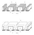
- FIGS. 1A and 1Bshow generally at 10 a unit cell according to an embodiment.
- the cellincludes a bottom electrode 12 electrically coupled to an access device 13 .
- the access deviceis electrically coupled to a word line (“WL”).
- WLword line
- the access deviceis a diode.
- An L-shaped memory material elementoverlies the bottom electrode 12 .
- the memory material elementhas an upright portion 17 and a base portion 15 .
- the base portion 15 in this exampleis in contact with a contact surface 16 of bottom electrode 12 .
- a narrow surface 18 of the upper end of the upright portion 17 of the L-shaped memory material element in this exampleis in contact with a contact surface of a top electrode 14 .
- the top electrodeconstitutes a bit line (“BL”).
- the current pathruns between the bottom electrode 12 and the top electrode 14 by way of the (fin-shaped) upright portion 17 of the memory element and, accordingly, this programmable resistance memory device may be referred a “fin-type” device.
- FIGS. 1C and 1Dshow generally at 11 a unit cell according to another embodiment.
- This cellis similar to that of FIGS. 1A and 1D and additionally includes a memory material layer 19 interposed between the upright portion 17 of the L-shaped memory material element and the top electrode 14 .
- the cellincludes a bottom electrode 12 electrically coupled to an access device 13 , electrically coupled to a word line (“WL”) which, in this example is a diode.
- WLword line
- An L-shaped memory material element overlying the bottom electrode 12has an upright portion 17 and a base portion 15 .
- the base portion 15 in this exampleis in contact with a contact surface 16 of bottom electrode 12 .
- a narrow surface 18 of the upper end of the upright portion 17 of the L-shaped memory material element in this exampleis in contact with a contact surface of the memory material layer 19 .
- the top electrodeconstitutes a bit line (“BL”).
- BLbit line
- This devicemay also be referred to as a fin-type device, as the current path runs between the bottom electrode 12 and the top electrode 14 by way of the (fin-shaped) upright portion 17 of the memory element and the memory material layer 19 .
- the interposed memory material layer 19can provide improved thermal isolation of the cells.
- FIGS. 1A , 1 B, 1 C and 1 Dshow.
- the volume of memory material in the memory elementcan be very small, having a thickness determined by the thickness of a deposited film of memory material.
- FIGS. 1B and 1Dmake reference to various dimensions that may be of interest. Particularly, the thickness (t mv ) of the fin-shaped upright portion 17 is very small, and the height (h m ) of the fin-shaped upright portion 17 is large.
- the thickness (t mv )can be as little as about 1 nm and may be in a range about 1 nm to about 50 nm, usually in a range about 5 nm to about 15 nm, and in particular examples about 8 nm; and in various embodiments the height (h m ) can be as little as about 10 nm and may be in a range about 10 nm to about 200 nm, usually in a range about 20 nm to about 100 nm, and in particular examples about 50 nm.
- the contact area of the surface 18 of the upright portion 17 with the upper electrode 14can be as small as about the square of the minimum feature size (for example, about 25 nm 2 where the minimum feature size is 5 nm), and may be in a range about 25 nm 2 to about 2500 nm 2 , usually in a range about 100 nm 2 to about 500 nm 2 , and in particular examples about 200 nm 2 .
- the minimum feature sizefor example, about 25 nm 2 where the minimum feature size is 5 nm
- Other dimensionsare discussed in the following description of stages in a method for fabricating a memory cell array according to an embodiment.
- FIG. 19is a schematic illustration of a memory array 190 , which can be implemented using memory cells as described herein.
- each memory cell 10includes a diode access device 198 and a fin-type programmable resistance memory element 196 (represented as a variable resistor) arranged in series along a current path between a corresponding word line 192 and a corresponding bit line 194 .
- the memory element in a given memory cellis programmable to a plurality of resistance states including a first and a second resistance state.
- the arraycomprises a plurality of word lines 192 including word lines 192 a , 192 b , and 192 c extending in parallel in a first direction, and a plurality of bit lines 194 including bit lines 194 a , 194 b , and 194 c extending in parallel in a second direction perpendicular to the first direction.
- the array 190is referred to as a cross-point array because the word lines 192 and bit lines 194 cross each other but do not physically intersect, and the memory cells 10 are located at these cross-point locations of the word lines 192 and bit lines 194 .
- Memory cell 10is representative of the memory cells of array 190 and is arranged at the cross-point location of the word line 192 b and the bit line 194 b , the memory cell 10 including a diode 198 and a memory element 196 arranged in series.
- the diode 198is electrically coupled to the word line 192 b and the memory element 196 is electrically coupled to the bit line 194 b.
- Reading or writing to memory cell 10 of array 190can be achieved by applying appropriate voltage pulses to the corresponding word line 192 b and bit line 194 b to induce a current through the selected memory cell 10 .
- the level and duration of the voltages appliedis dependent upon the operation performed, e.g., a reading operation or a programming operation.
- bias circuitryIn a read (or sense) operation of the data value stored in the memory cell 10 , bias circuitry (see, e.g., biasing arrangement supply voltages, current sources 236 of FIG. 20 ) coupled to the corresponding word line 192 b and bit line 194 b to apply bias arrangements across the memory cell 10 of suitable amplitude and duration to induce current to flow which does not result in the memory element 196 undergoing a change in resistive state.
- the current through the memory cell 10is dependent upon the resistance of the memory element 196 and, thus, upon the data value stored in the memory cell 10 .
- the data valuemay be determined, for example, by comparison of the current on the bit line 194 b with a suitable reference current by sense amplifiers (see, e.g., sense amplifiers/data in structures 224 of FIG. 20 ).
- bias circuitryIn a program operation of a data value to be stored in the memory cell 10 , bias circuitry (see, e.g., biasing arrangement supply voltages, current sources 236 of FIG. 20 ) coupled to the corresponding word line 192 b and bit line 194 b to apply bias arrangements across the memory cell 10 of suitable amplitude and duration to induce a programmable change in the memory element 196 to store the data value in the memory cell 10 , the electrical resistance of the memory element 196 corresponding to the data value stored in the memory cell 10 .
- bias circuitrysee, e.g., biasing arrangement supply voltages, current sources 236 of FIG. 20 ) coupled to the corresponding word line 192 b and bit line 194 b to apply bias arrangements across the memory cell 10 of suitable amplitude and duration to induce a programmable change in the memory element 196 to store the data value in the memory cell 10 , the electrical resistance of the memory element 196 corresponding to the data value stored in the memory cell 10 .
- the bias arrangementsinclude a first bias arrangement sufficient to forward bias the diode 198 and change the resistance state of the memory element 10 from a resistance corresponding to a first programmed state to a resistance corresponding to a second programmed state.
- the bias arrangementsalso include a second bias arrangement sufficient to forward bias the diode 198 and change the resistance state of the memory element 10 from a resistance corresponding to the second programmed state to a resistance corresponding to the first programmed state.
- the bias arrangements for unipolar operation of the memory element 10may each comprise one or more voltage pulses, and the voltage levels and pulse times can be determined empirically for each embodiment.
- FIG. 20is a simplified block diagram of an integrated circuit 201 including a cross-point memory array 190 of memory cells.
- each memory cellincludes a diode access device and a fin-type programmable resistance memory element as described herein.
- a word line (row) decoder 214is coupled to and in electrical communication with a plurality of word lines 216 .
- a bit line (column) decoder 218is in electrical communication with a plurality of bit lines 220 to read data from, and write data to, the memory cells (not shown) in array 190 . Addresses are supplied on bus 222 to word line decoder and drivers 214 and bit line decoder 218 .
- Sense amplifiers and data-in structures in block 224are coupled to bit line decoder 218 via data bus 226 .
- Dataare supplied via a data-in line 228 from input/output ports on integrated circuit 201 , or from other data sources internal or external to integrated circuit 201 , to data-in structures in block 224 .
- Other circuitry 230may be included on integrated circuit 201 , such as a general purpose processor or special purpose application circuitry, or a combination of modules providing system-on-a-chip functionality supported by array 190 .
- Dataare supplied via a data-out line 232 from the sense amplifiers in block 224 to input/output ports on integrated circuit 201 , or to other data destinations internal or external to integrated circuit 201 .
- Controller 234may be implemented using special-purpose logic circuitry as known in the art.
- controller 234comprises a general-purpose processor, which may be implemented on the same integrated circuit to execute a computer program to control the operations of the device.
- a combination of special-purpose logic circuitry and a general-purpose processormay be utilized for implementation of controller 234 .
- Embodiments of the programmable resistance material of the memory material elementinclude phase change based memory materials, including chalcogenide based materials and other materials.
- Chalcogensinclude any of the four elements oxygen (O), sulfur (S), selenium (Se), and tellurium (Te), forming part of group VIA of the periodic table.
- Chalcogenidescomprise compounds of a chalcogen with a more electropositive element or radical.
- Chalcogenide alloyscomprise combinations of chalcogenides with other materials such as transition metals.
- a chalcogenide alloyusually contains one or more elements from group IVA of the periodic table of elements, such as germanium (Ge) and tin (Sn).
- chalcogenide alloysinclude combinations including one or more of antimony (Sb), gallium (Ga), indium (In), and silver (Ag).
- Sbantimony
- Gagallium
- Inindium
- silversilver
- phase change based memory materialshave been described in technical literature, including alloys of: Ga/Sb, In/Se, Sb/Te, Ge/Te, Ge/Sb/Te, In/Sb/Te, Ga/Se/Te, Sn/Sb/Te, In/Sb/Ge, Ag/In/Sb/Te, Ge/Sn/Sb/Te, Ge/Sb/Se/Te and Te/Ge/Sb/S.
- a wide range of alloy compositionsmay be workable.
- compositionscan be characterized as Te a Ge b Sb 100-(a+b) .
- One researcherhas described the most useful alloys as having an average concentration of Te in the deposited materials well below 70%, typically below about 60% and ranged in general from as low as about 23% up to about 58% Te and most preferably about 48% to 58% Te.
- Concentrations of Gewere above about 5% and ranged from a low of about 8% to about 30% average in the material, remaining generally below 50%. Most preferably, concentrations of Ge ranged from about 8% to about 40%.
- the remainder of the principal constituent elements in this compositionwas Sb. These percentages are atomic percentages that total 100% of the atoms of the constituent elements. (Ovshinsky U.S. Pat. No.
- impuritiesmay be added to chalcogenides and other phase change materials in some embodiments to modify conductivity, transition temperature, melting temperature, and other properties of memory elements using the additive-modified chalcogenides.
- impurities used as additives for chalcogenidesinclude nitrogen, silicon, oxygen, silicon dioxide, silicon nitride, copper, silver, gold, aluminum, aluminum oxide, tantalum, tantalum oxide, tantalum nitride, titanium and titanium oxide. See, e.g., U.S. Pat. No. 6,800,504, and U.S. patent Application Publication No. U.S. 2005/0029502.
- Phase change alloysare capable of being switched between a first structural state in which the material is in a generally amorphous solid phase, and a second structural state in which the material is in a generally crystalline solid phase in its local order in the active channel region of the cell. These alloys are at least bistable.
- amorphousis used to refer to a relatively less ordered structure, more disordered than a single crystal, which has the detectable characteristics such as higher electrical resistivity than the crystalline phase.
- crystallineis used to refer to a relatively more ordered structure, more ordered than in an amorphous structure, which has detectable characteristics such as lower electrical resistivity than the amorphous phase.
- phase change materialsmay be electrically switched between different detectable states of local order across the spectrum between completely amorphous and completely crystalline states.
- Other material characteristics affected by the change between amorphous and crystalline phasesinclude atomic order, free electron density and activation energy.
- the materialmay be switched either into different solid phases or into mixtures of two or more solid phases, providing a gray scale between completely amorphous and completely crystalline states.
- the electrical properties in the materialmay vary accordingly.
- Phase change alloyscan be changed from one phase state to another by application of electrical pulses. It has been observed that a shorter, higher amplitude pulse tends to change the phase change material to a generally amorphous state. A longer, lower amplitude pulse tends to change the phase change material to a generally crystalline state. The energy in a shorter, higher amplitude pulse is high enough to allow for bonds of the crystalline structure to be broken and short enough to prevent the atoms from realigning into a crystalline state. Appropriate profiles for pulses can be determined, without undue experimentation, specifically adapted to a particular phase change alloy. In following sections of the disclosure, the phase change material is referred to as GST, and it will be understood that other types of phase change materials can be used. A material useful for implementation of a PCRAM described herein is Ge 2 Sb 2 Te 5 .
- RRAMresistance random access memory
- metal-oxidesincluding tungsten-oxide (WO x ), NiO, Nb 2 O 5 , CuO 2 , Ta 2 O 5 , Al 2 O 3 , CoO, Fe 2 O 3 , HfO 2 , TiO 2 , SrTiO 3 , SrZrO 3 , (BaSr)TiO 3 .
- MRAMmagnetoresistance random access memory
- STTspin-torque-transfer
- Additional examplesinclude solid electrolyte materials used for programmable-metallization-cell (PMC) memory, or nano-ionic memory, such as silver-doped germanium sulfide electrolytes and copper-doped germanium sulfide electrolytes.
- PMCprogrammable-metallization-cell
- nano-ionic memorysuch as silver-doped germanium sulfide electrolytes and copper-doped germanium sulfide electrolytes.
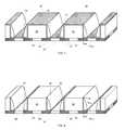
- FIGS. 2A , 2 B, and 3 - 12illustrate stages in fabrication of an array of programmable memory cells according to an embodiment.
- FIG. 2Ashows in a diagrammatic plan view a portion 20 of an array of bottom electrodes 22 exposed at the surface of a dielectric support 24 .
- FIG. 2Bshows a segment 21 of such an array, demarcated by broken lines 2 B in FIG. 2A .
- the segment 21includes six rows of two bottom electrodes, and two columns of six bottom electrodes.
- the bottom electrodes 22are electrically coupled to access devices formed in the underlying substrate (not shown in these Figures); the access devices coupled to the bottom electrodes in each row are coupled to a word line, and (as described further below) the memory cells in each column are couples to a bit line.
- Suitable materials for the bottom electrodes 22include conductive materials such as a metal or metal-based material or a non-metal material, such as, e.g.: copper; aluminum; titanium (Ti) and titanium-based materials such as titanium nitride (TiN), titanium ox nitride (TON); tantalum (Ta) and tantalum-based materials such as tantalum nitride (TaN); polysilicon, tungsten-based materials such as tungsten silicide (WSi x ); and, for a low thermal conductivity electrode, materials such as LNO (LaNiO3) and LSMO (LaSrMnO 3 ).
- conductive materialssuch as a metal or metal-based material or a non-metal material, such as, e.g.: copper; aluminum; titanium (Ti) and titanium-based materials such as titanium nitride (TiN), titanium ox nitride (TON); tantalum (Ta) and tantalum-
- Suitable materials for the dielectric support 24include, for example, materials employed as intermetallic dielectrics, and include oxides (such as, e.g., silicon dioxide).
- the upper surface of the bottom electrode arrayis planarized, for example by a CMP technique.
- the bottom electrodesmay have a thickness, for example, in a range about 1 nm to about 100 nm, more usually about 10 nm to about 50 nm, and in particular examples about 20 nm.
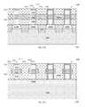
- FIG. 3shows a dielectric support layer 30 formed over the surface of the bottom electrode array.
- Suitable materials for the dielectric support layerinclude, for example, oxides (e.g., silicon oxides, such as SiO 2 ) and nitrides (e.g., silicon nitrides, such as SiN); low-K dielectric materials (such as a doped SiO 2 , for example) may be preferred; and materials having low thermal conductivity may be preferred.
- the dielectric support layercan be formed by, for example, a physical vapor deposition (PVD) process, or a chemical vapor deposition (CVD) process.
- PVDphysical vapor deposition
- CVDchemical vapor deposition
- cavitiesare formed in the dielectric support layer.
- the cavitiesexpose areas of the underlying bottom electrode array, and define dielectric support structures having sidewalls.
- the cavitiesare trenches 41 running parallel to the word lines in the access circuitry beneath the bottom electrode array.
- the dielectric support structures 40 defined by the trenches 41have generally vertical sidewalls 44 .
- the trenchesare arranged so that regions 42 of bottom electrodes 22 are exposed adjacent the sidewalls 44 ; and, in the example shown, the trenches are arranged and dimensioned so that regions 42 of bottom electrodes 22 are exposed adjacent the sidewalls 44 along both sides of each trench.
- the cavitiesare formed by, for example, a patterned etch such as a photolithography technique, or a reactive ion etch (RIE) technique. Where RIE is employed, it may be followed by a cleaning process.
- RIEreactive ion etch
- a suitable techniqueresults in substantially planar, approximately vertical sidewalls, and may be carried out in two or more steps.
- a film of the memory materialis formed over the upper surfaces and sidewalls of the dielectric support structures, and over the exposed areas of the bottom electrode array surface.
- a resulting structureis shown in FIG. 5 , in which the memory material film conformally covers, at 50 , the upper surfaces and, at 54 , the sidewalls, of the dielectric support structures 40 ; and conformally covers, at 51 , the exposed areas of the bottom electrode array.
- the memory material filmcontacts the exposed regions 42 of the bottom electrodes 22 .
- a chalcogenide materialis employed.
- the chalcogenide material filmmay be formed by vapor deposition, such as physical vapor deposition (PVD) or chemical vapor deposition (CVD), for example.
- PVDphysical vapor deposition
- CVDchemical vapor deposition
- An example of a method for forming a chalcogenide material filmuses a PVD-sputtering or magnetron-sputtering method with source gas(es) of Ar, N 2 , and/or He, etc. at the pressure in the range 1 mTorr ⁇ 100 mTorr.
- the depositionis usually done at room temperature.
- a collimator with an aspect ratio of 1 ⁇ 5can be used to improve the fill-in performance.
- a DC bias of several tens of volts to several hundreds of voltsmay also be used.
- the combination of DC bias and the collimatercan be used simultaneously.
- Another example of a method for forming a chalcogenide material filmuses CVD such as that disclosed in U.S. Patent Application Publication No. 2006/0172067, titled “Chemical Vapor Deposition of Chalcogenide Materials”, which is incorporated by reference herein.
- a post-deposition annealing treatment in a vacuum or in an N 2 ambientis optionally performed to improve the crystalline state of chalcogenide material.
- the annealing temperaturetypically ranges from 100° C. to 400° C. with an anneal time of less than 30 minutes.
- the memory material filmcan be formed to a thickness in a range about 1 nm to about 50 nm, more usually about 5 nm to about 15 nm, and in particular examples about 8 nm.
- the thickness of the memory film at 54on the sidewalls, establishes the eventual thickness (t mv ) of the fin-shaped upright portion 17 of the memory material element; and the thickness of the memory film at 51 , overlying the exposed areas 42 of the surfaces of the bottom electrodes 22 , establishes the eventual thickness (t mh ) of the base portion 15 of the memory material element.
- the fin-shaped upright portion of the memory material elementis also substantially planar, and may be referred to as planar herein.
- a dielectric sidewall spacer layeris formed over the memory material film.
- a resulting structureis shown in FIG. 6 , in which the dielectric sidewall spacer layer 60 covers the memory material film.
- Suitable materials for the dielectric sidewall spacer layerinclude, for example, a layer of oxide such as a silicon oxide (e.g., SiO 2 ), or a nitride such as a silicon nitride (e.g., SiN); low-K dielectric materials (such as a doped SiO 2 , for example) may be preferred. Preferred materials react only to a low extent or do not react with the memory material film; and preferred materials adhere well to the memory material film.
- a preferred sidewall spacer materialmay be SiN.
- the dielectric sidewall spacer layercan be formed by, for example, a vapor deposition process such as a chemical vapor deposition (CVD), or an atomic layer chemical vapor deposition (ALCVD), or an atomic layer deposition (ALD).
- the dielectric sidewall spacer layercan be formed to a thickness in a range about 1 nm to about 100 nm, more usually about 5 nm to about 30 nm, and in particular examples about 15 nm.
- dielectric sidewall spacersThereafter dielectric sidewall spacers are formed, and a memory material structure is formed having generally horizontal portions underlying the dielectric sidewall spacers (that is, between the dielectric sidewall spacers and the electrode array surface), and generally vertical portions between the dielectric sidewall spacers and the sidewalls of the dielectric support structures. Stated another way, the resulting memory material structure is L-shaped in a sectional view taken generally across the trenches.
- the dielectric sidewall spacersare formed by anisotropically etching the dielectric sidewall spacer 60 down to the memory material film. Suitable anisotropic etch techniques for formation of dielectric sidewall spacers include, for example, a directional plasma etch, for example a reactive ion etch (RIE).
- RIEreactive ion etch
- a resulting structureis shown in FIG. 7 , showing dielectric sidewall spacers 74 in the inner angles defined at the intersection of the memory material film 54 on the sidewalls 44 of the dielectric support structures 40 and the memory material film 51 on the exposed areas of the bottom electrode array.
- the dielectric sidewall spacerhas a width (w ss ) at the bottom electrode array.
- the width (w ss )depends upon, among other factors, the thickness of the dielectric sidewall spacer layer; additionally, the width of the dielectric sidewall spacers can be controlled by selecting etch parameters (power, pressure, reaction chemistry) according to the particular material being etched.
- the anisotropic etch of the dielectric sidewall spacer layer 60exposes areas of the memory material film at 50 , the upper surfaces of the dielectric support structures 40 , and at 71 over areas of the bottom electrode array surface not overlain by the sidewall spacers 74 .
- This anisotropic etchmay be continued through the exposed areas of the memory film; or, the exposed areas of the memory material film may be removed by a subsequent etching step.
- the memory materialis a GST-type phase change material, for example, it may be preferred to avoid use of Chlorine-based etch chemistry for removal of exposed areas of the memory material film.
- FIG. 8A resulting structure is shown in FIG. 8 .
- the memory material filmhas generally horizontal portions 85 underlying the dielectric sidewall spacers and generally vertical portions 87 between the dielectric sidewall spacers and the sidewalls of the dielectric support structures.
- the height (h ms ) of the vertical portions 87 at this stageis approximately equal to the height of the dielectric support structures 40 ; and the width (w ms ) of the generally horizontal portions 85 at this stage is approximately equal to the widths (w ss ) of the dielectric sidewall spacers 74 .
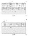
- a dielectric fillis formed in the trenches and over the structure of FIG. 8 , as shown at 90 is FIG. 9 .
- Suitable materials for the dielectric fillinclude, for example, oxides such as silicon oxides, or nitrides such as silicon nitrides; low-K dielectrics may be preferred.
- the dielectric fillcan be formed by, for example, deposition of a suitable fill material.
- FIG. 9Thereafter the structure of FIG. 9 is planarized by, for example CMP, to form a structure as shown in FIG. 10 .
- the height of the features in the resulting planarized structure(including dielectric support structures 144 , dielectric fills 100 , dielectric sidewall spacers 104 , and the vertical portions 117 of the memory material structures 115 , 117 ) may as a result of the polish be less than the height (h ms ) of the dielectric support structures 40 prior to planarization.
- Planarizationexposes upper surfaces of the dielectric support structures 144 , of the dielectric fills 100 , truncated upper edges of the dielectric sidewall spacers 104 , and surfaces 107 of the upper ends of the vertical portions 117 of the memory material structures.
- the planarizationhas no effect on the width (w ms ) of the generally horizontal portions 115 of the memory material structures.
- the contact surfaces 107are generally planar, and lie in a plane generally parallel to the plane of the bottom electrodes, and transverse to the vertical portions 117 of the L-shaped memory material structures.
- Suitable materials for the top electrode layerinclude conductive materials such as a metal or metal-based material or a non-metal material, such as, e.g.: copper; aluminum; titanium (Ti) and titanium-based materials such as titanium nitride (TiN), titanium ox nitride (TON); tantalum (Ta) and tantalum-based materials such as tantalum nitride (TaN); polysilicon, tungsten-based materials such as tungsten silicide (WSi x ); and, for a low thermal conductivity electrode, materials such as LNO (LaNiO3) and LSMO (LaSrMnO 3 ).
- the top electrode layermay be formed by any of a variety of techniques suited to the particular material. Such techniques include, by way of example, sputtering and plating and CVD.
- top electrode materialis patterned to form top electrodes over the memory cells.
- the top electrodesmay be patterned to form islands; or, as in the example shown in FIG. 12 , they may be formed as straplines or bitlines 114 , generally perpendicular to the underlying word lines.
- the top electrodemay have a thickness, for example, in a range about 200 ⁇ to about 5000 ⁇ , usually about 2000 ⁇ .
- the patterned top electrodescontact the upper surfaces 107 (see, e.g., FIG. 10 ) of the memory material structures 115 , 117 , establishing a current path running through the fin-shaped memory material element between the lower and upper electrodes.
- trenchese.g., trench 120
- the trenchis formed to a depth sufficient to cut through the memory material structures, resulting in separate columns of individual memory material elements.
- the trenchmay stop at the bottom electrode layer; or, as shown in FIG. 12 , the trench may go through the bottom electrode layer as well. In any event the trench must not pass through the underlying word lines.
- the top electrodesmay be patterned by, for example, an etch (by, for example, a photolithography technique) prior to forming the trenches. Or where, as here, the top electrodes are formed as straplines or bitlines, the top electrodes may be patterned as part of the trench formation. Where the top electrodes are patterned as part of the trench formation (using the same mask), the top electrodes are self-aligned with the memory material structures.
- Suitable techniques for forming the trenchinclude, for example, a directional etch such as, for example an RIE.
- the RIEmay be controlled by selection of process parameters; employing lower pressure and higher substrate bias may provide better control of the shape and dimensions of the trench.
- a double-patterning or manifold patterning lithographic techniquemay be employed; examples of such techniques are outlined in Ping Xie et al. (2009) “Analysis of higher-order pitch division for sub-32 nm lithography”, Proc. of SPIE, Vol. 7274, pp. 72741Y-1 through 72741Y-8.
- a layer of a memory materialmay be interposed between the planarized surface of the structure of FIG. 10 and the top electrode layer, as illustrated for example in FIGS. 13-15 .
- a layer 130 of a memory materialis formed over the surface of the structure of FIG. 10 .
- the memory material of layer 130may be any of the variety of memory materials outlined above.
- the memory material of layer 130may the same materials as, or the same type of material as, the memory material of the memory material structures 115 , 117 .
- a top electrode material layer 140is formed as described above over the memory material layer 130 , as shown in FIG. 14 .
- top electrode materialis patterned to form top electrodes over the memory cells.
- the top electrodesmay be patterned to form islands; or, as in the example shown in FIG. 15 , they may be formed as straplines or bitlines 114 , generally perpendicular to the underlying word lines.
- the top electrodemay have a thickness, for example, in a range about 200 ⁇ to about 5000 ⁇ , usually about 2000 ⁇ .
- trenchese.g., trench 120
- trenchesare formed perpendicular to the underlying word lines and between the top electrodes and the memory material layer 130 to separate the columns of memory cells.
- the trenchpasses through the memory material layer, resulting in lines of memory material 119 underlying the top electrodes 114 , as shown in FIG. 15 .
- the trenchis formed to a depth sufficient to cut through the memory material structures, resulting in separate columns of individual memory material elements.
- the trenchmay stop at the bottom electrode layer; or, as shown in FIG. 15 , the trench may go through the bottom electrode layer as well. In any event the trench must not pass through the underlying word lines.
- the top electrodesmay be patterned by, for example, an etch (by, for example, a photolithography technique) prior to forming the trenches. Or where, as here, the top electrodes are formed as straplines or bitlines, the top electrodes may be patterned as part of the trench formation and, as noted above, where the top electrodes are patterned as part of the trench formation (using the same mask), the top electrodes are self-aligned with the memory material structures. Examples of suitable techniques for patterning the top electrodes and for forming the trenches, are outlined above.
- the widths of the top electrodesmay be the same as, or greater or less than, the width of the memory elements underlying it.
- the top electrodes and the underlying memory elementsare self-aligned, and where the etch is highly directional, the widths of the top electrodes and of the underlying memory elements are the same.
- the etch processmay be modified to provide a controlled degree of undercut of the underlying memory material, resulting in the memory elements being narrower than the top electrodes.
- the top electrodesmay be made narrower than the underlying memory elements, either (for example) by employing different masks for patterning the top electrodes and forming the trenches or (for example) by narrowing the top electrodes in a subsequent procedure.
- the width (w bl ) of the top electrode 114is equal to or is greater than the width (w mv ) of the upright portion 17 of the underlying memory element
- the area of contact between the upright portion 17 of the memory element and the upper electrode 14 ( 114 )is the area of the contact surface 18 . That is, the contact area is the product of the thickness (t mv ) and the width (w mv ) of the upright portion 17 of the memory material element).
- the width (w bl ) of the top electrode 114is less than the width (w mv ) of the upright portion 17 of the underlying memory element
- the area of contact between the upright portion 17 of the memory element and the upper electrode 14 ( 114 )is the product of the thickness (t mv ) of the upright portion 17 of the memory element and the width (w bl ) of the top electrode 14 ( 114 ).
- a dielectric fill(not shown in the Figures) is deposited in the trenches and over the top electrodes.
- FIGS. 16-18Each of these Figures shows a portion of a column of memory cells electrically coupled to a top electrode that constitutes a bit line.
- the access devices 160 in FIG. 16are diodes; the access devices 170 in FIG. 17 are field effect transistors; the access devices 180 in FIG. 18 are bipolar junction transistors.
- Various configurations for access circuitryare known, along with methods for fabricating them, and others are contemplated. Examples include vertical silicon-based drives.
- FIGS. 21A , 21 B, 21 Cillustrate an example of access devices that may suitably employed.
- FIG. 21Ais a plan view of a portion of the access device array
- FIG. 21Bis a section thru a portion of the array at B-B′ in FIG. 1A , taken along a word line 2130
- FIG. 21Cis a section thru a portion of the array at C-C′ in FIG. 1A , taken along a bit line 2120 .
- the access device array 2101includes a single-crystalline substrate 2100 comprising a well 2105 having a first conductivity type and conductive lines 2120 ( 2120 a , 2120 b , 2120 c , 2120 d ) (which may constitute bit lines) within the well 2105 .
- the conductive lines 2120extend in a first direction into out of the sectional view of FIG. 21B and are separated by dielectric trench isolation structures 2132 within the well 2105 .
- the conductive lines 2120comprise doped substrate material having a second conductivity type opposite that of the first conductivity type.
- the doped substrate material of the conductive lines 2120comprises high doped N-type (N+) material of the substrate 2100
- the well 2105comprises doped P-type material of the substrate 2100 .
- the field effect transistor 2115 of the access deviceincludes a first terminal 2122 comprising doped semiconductor material on the corresponding conductive line 2120 b , a channel region 2123 comprising doped semiconductor material on the first terminal 2122 , and a second terminal 2124 comprising doped semiconductor material on the channel region 2123 .
- a conductive cap 2127 comprising silicideis on the second terminal 2124 .
- the conductive cap 2127may comprise, for example, a silicide containing Ti, W, Co, Ni, or Ta.
- the conductive cap 2127provides a low resistance contact between the doped semiconductor material of the second terminal 2126 and an electrode 22 in the overlying electrode array (not shown in these Figures; see electrodes 22 in FIGS. 2A , 2 B).
- first and second terminals 2122 , 2124comprise highly doped N-type material, and the channel region 2123 comprises doped P-type material.
- the first and second terminals 2122 , 2124 , the channel region 2123 , and the conductive cap 2127form a stack which is surrounded by a dielectric 2230 , the dielectric 2230 separating the channel region 2123 from the corresponding word line 2130 b.
- the word lines 2130extend into and out of the sectional view of FIG. 21C and comprise doped polysilicon material and a silicide layer on the doped polysilicon.
- the stack formed by the first and second terminals 2122 , 2124 , the channel region 2123 , and the conductive cap 2127extends through a via in the word line 2130 b to electrically couple the conductive line 2120 b to an overlying electrode, the via in the word line 2130 b having a sidewall surface 2135 surrounding the channel region 2123 .
- the memory cell arrayis formed over the access device array shown in FIGS. 21A , 21 B, 21 C.
- the conductive cap 2127may itself constitute the bottom electrode of the memory cell that is formed over it.
- an overlying electrode layer(not shown in these Figures; see FIGS. 2A , 2 B) may be provided, including electrodes 22 formed in contact with the conductive caps 2127 and extending through a dielectric 24 to the memory element.
- a common voltage coupled to the conductive material (top electrode) 14 and voltages supplied to the word line 2130 b and the conductive (bit) line 2120 bcan induce current to flow from the conductive line 2120 b to the conductive material 14 , or vice versa, by way of the first terminal 2122 , channel region 2123 , second terminal 2124 , conductive cap 2127 , bottom electrode 12 , memory material element 15 , 17 and memory material layer 19 .
- FIGS. 22A , 22 Billustrate another example of access devices that may suitably employed.
- FIG. 22Ais a section thru a portion of the array, taken perpendicular to a bit line 2320 ; and
- FIG. 22Bis a section thru a portion of the array, taken along a bit line 2320 .
- the access device array 2301includes a single-crystalline substrate 2300 comprising a well 2305 having a first conductivity type and conductive lines 2320 ( 2320 a , 2320 b , 2320 c , 2320 d ) (which may constitute bit lines) within the well 2305 .
- the conductive lines 2320extend in a first direction into out of the sectional view of FIG. 22A and are separated by dielectric trench isolation structures 2332 within the well 2305 .
- the conductive lines 2320comprise doped substrate material having a second conductivity type opposite that of the first conductivity type.
- the doped substrate material of the conductive lines 2320comprises high doped N-type (N+) material of the substrate 2300
- the well 2305comprises doped P-type material of the substrate 2300
- Access devices 2315extend upwardly from the corresponding conductive lines, within vias surrounded by dielectric fill material 2330 .
- Each access device 2315includes, successively from the conductive lines 2320 upward, a lightly doped layer of N material (the N ⁇ layer) 2322 , a layer of heavily doped P material (the P+ layer) 2323 , and a conductive cap 2327 .
- the memory cell arrayis formed over the access device array shown in FIGS. 22A , 22 B.
- the conductive cap 2327may itself constitute the bottom electrode of the memory cell that is formed over it.
- an overlying electrode layer(not shown in these Figures; see FIGS. 2A , 2 B) may be provided, including electrodes 22 formed in contact with the conductive caps 2327 and extending through a dielectric 24 to the memory element.
- the structuredefines a transistor; and in FIGS. 22A , 22 B the N ⁇ and P+ layers define a diode.
- the structureis constructed vertically, and can be fabricated to a high device density.
- FIG. 1depicts a portion of an array, showing four adjacent elements in a row or column of a 4 ⁇ 4 portion of an array.
- the various elementsare shown without the components required to connect them to other circuitry within or without the semiconductor chip in which they are embedded.
- the arraymay be scaled up to several billion elements or more.
- the active region of the memory elementin which the memory material is induced to change between at least two solid phases, is located within the upright portion 17 .
- the active regioncan be made extremely small in the illustrated structure, thus reducing the magnitude of current needed to induce a phase change.
- the thickness t mv of the memory material 17can be established using thin film deposition techniques, as described above.
- the width w mv of the memory material fin 17is formed using the same mask as is used to pattern the top electrode (that is, the top electrode and the memory material fin width are “self-aligned”), the width w mv can be made less than that of the top electrode 14 , and preferably less than a minimum feature size for a process, typically a lithographic process, used to form the top electrodes.
- the resulting memory material fin 17has a thin and narrow cross-sectional area, and a correspondingly thin and narrow top surface 18 contacting the memory material layer 19 .
- the small sectional area and top surface of the memory material fin 17concentrates current density, thereby reducing the magnitude of the current needed to induce a phase change in the active region. Additionally, the dielectric adjacent the fin may provide some thermal isolation to the active region, which also helps to reduce the amount of current necessary to induce a phase change.
Landscapes
- Engineering & Computer Science (AREA)
- Manufacturing & Machinery (AREA)
- Chemical & Material Sciences (AREA)
- Materials Engineering (AREA)
- Semiconductor Memories (AREA)
Abstract
Description
Claims (11)
Priority Applications (4)
| Application Number | Priority Date | Filing Date | Title |
|---|---|---|---|
| US12/778,897US8729521B2 (en) | 2010-05-12 | 2010-05-12 | Self aligned fin-type programmable memory cell |
| TW099127790ATWI442612B (en) | 2010-05-12 | 2010-08-19 | Self aligned fin-type programmable memory cell |
| CN201010504900.1ACN102244194B (en) | 2010-05-12 | 2010-10-09 | Self-aligned Fin-Type Programmable Memory Cell |
| US14/281,192US8853047B2 (en) | 2010-05-12 | 2014-05-19 | Self aligned fin-type programmable memory cell |
Applications Claiming Priority (1)
| Application Number | Priority Date | Filing Date | Title |
|---|---|---|---|
| US12/778,897US8729521B2 (en) | 2010-05-12 | 2010-05-12 | Self aligned fin-type programmable memory cell |
Related Child Applications (1)
| Application Number | Title | Priority Date | Filing Date |
|---|---|---|---|
| US14/281,192DivisionUS8853047B2 (en) | 2010-05-12 | 2014-05-19 | Self aligned fin-type programmable memory cell |
Publications (2)
| Publication Number | Publication Date |
|---|---|
| US20110278528A1 US20110278528A1 (en) | 2011-11-17 |
| US8729521B2true US8729521B2 (en) | 2014-05-20 |
Family
ID=44910946
Family Applications (2)
| Application Number | Title | Priority Date | Filing Date |
|---|---|---|---|
| US12/778,897Active2032-08-04US8729521B2 (en) | 2010-05-12 | 2010-05-12 | Self aligned fin-type programmable memory cell |
| US14/281,192ActiveUS8853047B2 (en) | 2010-05-12 | 2014-05-19 | Self aligned fin-type programmable memory cell |
Family Applications After (1)
| Application Number | Title | Priority Date | Filing Date |
|---|---|---|---|
| US14/281,192ActiveUS8853047B2 (en) | 2010-05-12 | 2014-05-19 | Self aligned fin-type programmable memory cell |
Country Status (3)
| Country | Link |
|---|---|
| US (2) | US8729521B2 (en) |
| CN (1) | CN102244194B (en) |
| TW (1) | TWI442612B (en) |
Cited By (7)
| Publication number | Priority date | Publication date | Assignee | Title |
|---|---|---|---|---|
| US20140097398A1 (en)* | 2010-10-29 | 2014-04-10 | Hans S. Cho | Memristive devices and memristors with ribbon-like junctions and methods for fabricating the same |
| US8853047B2 (en) | 2010-05-12 | 2014-10-07 | Macronix International Co., Ltd. | Self aligned fin-type programmable memory cell |
| US20140322910A1 (en)* | 2012-05-01 | 2014-10-30 | Taiwan Semiconductor Manufacturing Company, Ltd. | Via-free interconnect structure with self-aligned metal line interconnections |
| US9711217B1 (en)* | 2016-01-20 | 2017-07-18 | Macronix International Co., Ltd. | Memory device and operating method for resistive memory cell |
| US9768232B2 (en) | 2016-02-22 | 2017-09-19 | Samsung Electronics Co., Ltd. | Variable resistance memory device and a method of manufacturing the same |
| US20190157554A1 (en)* | 2017-11-13 | 2019-05-23 | Taiwan Semiconductor Manufacturing Co., Ltd. | Novel resistive random access memory device |
| US11957069B2 (en) | 2021-10-22 | 2024-04-09 | International Business Machines Corporation | Contact resistance of a metal liner in a phase change memory cell |
Families Citing this family (29)
| Publication number | Priority date | Publication date | Assignee | Title |
|---|---|---|---|---|
| KR20120104031A (en)* | 2011-03-11 | 2012-09-20 | 삼성전자주식회사 | Phase change material layer, method of forming a phase change layer, phase change memory device and method of manufacturing a phase change memory device |
| US20130058158A1 (en)* | 2011-09-01 | 2013-03-07 | Micron Technology, Inc. | Method, system, and device for l-shaped memory component |
| US8728940B2 (en) | 2012-01-26 | 2014-05-20 | Micron Technology, Inc. | Memory arrays and methods of forming same |
| US9136307B2 (en) | 2012-02-09 | 2015-09-15 | Micron Technology, Inc. | Memory cells and memory cell formation methods using sealing material |
| US9491118B1 (en)* | 2012-04-04 | 2016-11-08 | The United States Of America As Represented By The Administrator Of National Aeronautics And Space Administration | Wireless nanoionic-based radio frequency switch |
| US8885382B2 (en) | 2012-06-29 | 2014-11-11 | Intel Corporation | Compact socket connection to cross-point array |
| US8853665B2 (en)* | 2012-07-18 | 2014-10-07 | Micron Technology, Inc. | Semiconductor constructions, memory cells, memory arrays and methods of forming memory cells |
| JP2014022548A (en)* | 2012-07-18 | 2014-02-03 | Ps4 Luxco S A R L | Semiconductor device and manufacturing method of the same |
| US9166159B2 (en)* | 2013-05-23 | 2015-10-20 | Micron Technology, Inc. | Semiconductor constructions and methods of forming memory cells |
| US9443763B2 (en) | 2013-09-12 | 2016-09-13 | Micron Technology, Inc. | Methods for forming interconnections between top electrodes in memory cells by a two-step chemical-mechanical polishing (CMP) process |
| US9257431B2 (en) | 2013-09-25 | 2016-02-09 | Micron Technology, Inc. | Memory cell with independently-sized electrode |
| US20160181517A1 (en)* | 2014-12-23 | 2016-06-23 | Silicon Storage Technology, Inc. | Geometrically Enhanced Resistive Random Access Memory (RRAM) Cell And Method Of Forming Same |
| US9305974B1 (en) | 2015-04-16 | 2016-04-05 | Stmicroelectronics, Inc. | High density resistive random access memory (RRAM) |
| US9318392B1 (en) | 2015-06-18 | 2016-04-19 | International Business Machines Corporation | Method to form SOI fins on a bulk substrate with suspended anchoring |
| US9299924B1 (en)* | 2015-06-29 | 2016-03-29 | International Business Machines Corporation | Injection pillar definition for line MRAM by a self-aligned sidewall transfer |
| US9653127B1 (en)* | 2015-12-15 | 2017-05-16 | Micron Technology, Inc. | Methods and apparatuses for modulating threshold voltages of memory cells |
| US10424619B2 (en)* | 2016-01-13 | 2019-09-24 | Samsung Electronics Co., Ltd. | Variable resistance memory devices and methods of manufacturing the same |
| US9780301B1 (en)* | 2016-04-15 | 2017-10-03 | Taiwan Semiconductor Manufacturing Company Ltd. | Method for manufacturing mixed-dimension and void-free MRAM structure |
| CN106299112B (en)* | 2016-08-18 | 2019-06-18 | 中国科学院上海微系统与信息技术研究所 | Multistate phase change memory cell device and method of making the same |
| US10424374B2 (en) | 2017-04-28 | 2019-09-24 | Micron Technology, Inc. | Programming enhancement in self-selecting memory |
| KR102593112B1 (en) | 2017-10-23 | 2023-10-25 | 삼성전자주식회사 | Variable resistance memory device and method of forming the same |
| US10693065B2 (en) | 2018-02-09 | 2020-06-23 | Micron Technology, Inc. | Tapered cell profile and fabrication |
| US10854813B2 (en) | 2018-02-09 | 2020-12-01 | Micron Technology, Inc. | Dopant-modulated etching for memory devices |
| US10541364B2 (en) | 2018-02-09 | 2020-01-21 | Micron Technology, Inc. | Memory cells with asymmetrical electrode interfaces |
| US10424730B2 (en)* | 2018-02-09 | 2019-09-24 | Micron Technology, Inc. | Tapered memory cell profiles |
| US11730070B2 (en) | 2019-02-27 | 2023-08-15 | International Business Machines Corporation | Resistive random-access memory device with step height difference |
| CN111599917B (en)* | 2020-05-29 | 2023-03-14 | 江苏时代全芯存储科技股份有限公司 | Manufacturing method of phase change memory |
| TWI865720B (en)* | 2021-02-01 | 2024-12-11 | 聯華電子股份有限公司 | Rram device and forming method thereof |
| CN113284954B (en)* | 2021-07-22 | 2021-09-24 | 成都蓉矽半导体有限公司 | A kind of high channel density silicon carbide MOSFET and preparation method thereof |
Citations (337)
| Publication number | Priority date | Publication date | Assignee | Title |
|---|---|---|---|---|
| US3271591A (en) | 1963-09-20 | 1966-09-06 | Energy Conversion Devices Inc | Symmetrical current controlling device |
| US3530441A (en) | 1969-01-15 | 1970-09-22 | Energy Conversion Devices Inc | Method and apparatus for storing and retrieving information |
| US3846767A (en) | 1973-10-24 | 1974-11-05 | Energy Conversion Devices Inc | Method and means for resetting filament-forming memory semiconductor device |
| US4452592A (en) | 1982-06-01 | 1984-06-05 | General Motors Corporation | Cyclic phase change coupling |
| US4599705A (en) | 1979-12-13 | 1986-07-08 | Energy Conversion Devices, Inc. | Programmable cell for use in programmable electronic arrays |
| US4719594A (en) | 1984-11-01 | 1988-01-12 | Energy Conversion Devices, Inc. | Grooved optical data storage device including a chalcogenide memory layer |
| US4769339A (en) | 1983-12-26 | 1988-09-06 | Kabushiki Kaisha Toshiba | Method of manufacturing a field effect transistor device having a multilayer gate electrode |
| US4876220A (en) | 1986-05-16 | 1989-10-24 | Actel Corporation | Method of making programmable low impedance interconnect diode element |
| US4959812A (en) | 1987-12-28 | 1990-09-25 | Kabushiki Kaisha Toshiba | Electrically erasable programmable read-only memory with NAND cell structure |
| US5106775A (en) | 1987-12-10 | 1992-04-21 | Hitachi, Ltd. | Process for manufacturing vertical dynamic random access memories |
| US5166758A (en) | 1991-01-18 | 1992-11-24 | Energy Conversion Devices, Inc. | Electrically erasable phase change memory |
| US5166096A (en) | 1991-10-29 | 1992-11-24 | International Business Machines Corporation | Process for fabricating self-aligned contact studs for semiconductor structures |
| US5177567A (en) | 1991-07-19 | 1993-01-05 | Energy Conversion Devices, Inc. | Thin-film structure for chalcogenide electrical switching devices and process therefor |
| US5332923A (en) | 1991-08-06 | 1994-07-26 | Nec Corporation | Semiconductor memory |
| US5391901A (en) | 1992-10-30 | 1995-02-21 | Nec Corporation | Semiconductor memory with oblique folded bit-line arrangement |
| US5515488A (en) | 1994-08-30 | 1996-05-07 | Xerox Corporation | Method and apparatus for concurrent graphical visualization of a database search and its search history |
| US5534712A (en) | 1991-01-18 | 1996-07-09 | Energy Conversion Devices, Inc. | Electrically erasable memory elements characterized by reduced current and improved thermal stability |
| US5550396A (en) | 1992-01-24 | 1996-08-27 | Mitsubishi Denki Kabushiki Kaisha | Vertical field effect transistor with a trench structure |
| US5687112A (en) | 1996-04-19 | 1997-11-11 | Energy Conversion Devices, Inc. | Multibit single cell memory element having tapered contact |
| US5688713A (en) | 1996-08-26 | 1997-11-18 | Vanguard International Semiconductor Corporation | Method of manufacturing a DRAM cell having a double-crown capacitor using polysilicon and nitride spacers |
| US5716883A (en) | 1996-11-06 | 1998-02-10 | Vanguard International Semiconductor Corporation | Method of making increased surface area, storage node electrode, with narrow spaces between polysilicon columns |
| US5754472A (en) | 1995-12-27 | 1998-05-19 | Hyundai Electronics Industries Co., Ltd. | Flash memory device having a program path the same as a read pre-condition path |
| US5789277A (en) | 1996-07-22 | 1998-08-04 | Micron Technology, Inc. | Method of making chalogenide memory device |
| US5789758A (en) | 1995-06-07 | 1998-08-04 | Micron Technology, Inc. | Chalcogenide memory cell with a plurality of chalcogenide electrodes |
| US5814527A (en) | 1996-07-22 | 1998-09-29 | Micron Technology, Inc. | Method of making small pores defined by a disposable internal spacer for use in chalcogenide memories |
| US5831276A (en) | 1995-06-07 | 1998-11-03 | Micron Technology, Inc. | Three-dimensional container diode for use with multi-state material in a non-volatile memory cell |
| US5837564A (en) | 1995-11-01 | 1998-11-17 | Micron Technology, Inc. | Method for optimal crystallization to obtain high electrical performance from chalcogenides |
| US5869843A (en) | 1995-06-07 | 1999-02-09 | Micron Technology, Inc. | Memory array having a multi-state element and method for forming such array or cells thereof |
| US5879955A (en) | 1995-06-07 | 1999-03-09 | Micron Technology, Inc. | Method for fabricating an array of ultra-small pores for chalcogenide memory cells |
| US5902704A (en) | 1997-07-02 | 1999-05-11 | Lsi Logic Corporation | Process for forming photoresist mask over integrated circuit structures with critical dimension control |
| US5933365A (en) | 1997-06-19 | 1999-08-03 | Energy Conversion Devices, Inc. | Memory element with energy control mechanism |
| US5952671A (en) | 1997-05-09 | 1999-09-14 | Micron Technology, Inc. | Small electrode for a chalcogenide switching device and method for fabricating same |
| US5958358A (en) | 1992-07-08 | 1999-09-28 | Yeda Research And Development Co., Ltd. | Oriented polycrystalline thin films of transition metal chalcogenides |
| US5970336A (en) | 1996-08-22 | 1999-10-19 | Micron Technology, Inc. | Method of making memory cell incorporating a chalcogenide element |
| US5985698A (en) | 1996-07-22 | 1999-11-16 | Micron Technology, Inc. | Fabrication of three dimensional container diode for use with multi-state material in a non-volatile memory cell |
| US6011725A (en) | 1997-08-01 | 2000-01-04 | Saifun Semiconductors, Ltd. | Two bit non-volatile electrically erasable and programmable semiconductor memory cell utilizing asymmetrical charge trapping |
| US6025220A (en) | 1996-06-18 | 2000-02-15 | Micron Technology, Inc. | Method of forming a polysilicon diode and devices incorporating such diode |
| US6031287A (en) | 1997-06-18 | 2000-02-29 | Micron Technology, Inc. | Contact structure and memory element incorporating the same |
| US6034882A (en) | 1998-11-16 | 2000-03-07 | Matrix Semiconductor, Inc. | Vertically stacked field programmable nonvolatile memory and method of fabrication |
| US6046951A (en) | 1998-01-23 | 2000-04-04 | Stmicroelectronics S.A. | Process for controlling the read circuit of a memory plane and corresponding memory device |
| US6066870A (en) | 1996-07-16 | 2000-05-23 | Micron Technology, Inc. | Single digit line with cell contact interconnect |
| US6075719A (en) | 1999-06-22 | 2000-06-13 | Energy Conversion Devices, Inc. | Method of programming phase-change memory element |
| US6077674A (en) | 1999-10-27 | 2000-06-20 | Agilent Technologies Inc. | Method of producing oligonucleotide arrays with features of high purity |
| US6087269A (en) | 1998-04-20 | 2000-07-11 | Advanced Micro Devices, Inc. | Method of making an interconnect using a tungsten hard mask |
| US6087674A (en) | 1996-10-28 | 2000-07-11 | Energy Conversion Devices, Inc. | Memory element with memory material comprising phase-change material and dielectric material |
| US6114713A (en) | 1997-01-28 | 2000-09-05 | Zahorik; Russell C. | Integrated circuit memory cell having a small active area and method of forming same |
| US6117720A (en) | 1995-06-07 | 2000-09-12 | Micron Technology, Inc. | Method of making an integrated circuit electrode having a reduced contact area |
| US6147395A (en) | 1996-10-02 | 2000-11-14 | Micron Technology, Inc. | Method for fabricating a small area of contact between electrodes |
| US6177317B1 (en) | 1999-04-14 | 2001-01-23 | Macronix International Co., Ltd. | Method of making nonvolatile memory devices having reduced resistance diffusion regions |
| WO2001045108A1 (en) | 1999-12-16 | 2001-06-21 | Ovonyx, Inc. | Programmable resistance memory arrays with reference cells |
| US6271090B1 (en) | 2000-12-22 | 2001-08-07 | Macronix International Co., Ltd. | Method for manufacturing flash memory device with dual floating gates and two bits per cell |
| US6280684B1 (en) | 1994-12-13 | 2001-08-28 | Ricoh Company, Ltd. | Sputtering target, method of producing the target, optical recording medium fabricated by using the sputtering target, and method of fabricating the optical recording medium |
| US6291137B1 (en) | 1999-01-20 | 2001-09-18 | Advanced Micro Devices, Inc. | Sidewall formation for sidewall patterning of sub 100 nm structures |
| US6316348B1 (en) | 1999-02-05 | 2001-11-13 | Taiwan Semiconductor Manufacturing Company | High selectivity Si-rich SiON etch-stop layer |
| US6320786B1 (en) | 2000-12-22 | 2001-11-20 | Macronix International Co., Ltd. | Method of controlling multi-state NROM |
| US6326307B1 (en) | 1999-11-15 | 2001-12-04 | Appllied Materials, Inc. | Plasma pretreatment of photoresist in an oxide etch process |
| US6337266B1 (en) | 1996-07-22 | 2002-01-08 | Micron Technology, Inc. | Small electrode for chalcogenide memories |
| US6339544B1 (en) | 2000-09-29 | 2002-01-15 | Intel Corporation | Method to enhance performance of thermal resistor device |
| US20020017701A1 (en) | 1999-03-25 | 2002-02-14 | Patrick Klersy | Electrically programmable memory element with raised pore |
| US6351406B1 (en) | 1998-11-16 | 2002-02-26 | Matrix Semiconductor, Inc. | Vertically stacked field programmable nonvolatile memory and method of fabrication |
| US6372651B1 (en) | 1998-07-17 | 2002-04-16 | Advanced Micro Devices, Inc. | Method for trimming a photoresist pattern line for memory gate etching |
| US6380068B2 (en) | 2000-01-05 | 2002-04-30 | Macronix International Co., Ltd. | Method for planarizing a flash memory device |
| US20020070457A1 (en) | 2000-12-09 | 2002-06-13 | Samsung Electronics Co., Ltd. | Metal contact structure in semiconductor device and method for forming the same |
| US6420216B1 (en) | 2000-03-14 | 2002-07-16 | International Business Machines Corporation | Fuse processing using dielectric planarization pillars |
| US6420215B1 (en) | 2000-04-28 | 2002-07-16 | Matrix Semiconductor, Inc. | Three-dimensional memory array and method of fabrication |
| US6429064B1 (en) | 2000-09-29 | 2002-08-06 | Intel Corporation | Reduced contact area of sidewall conductor |
| US20020113273A1 (en) | 2001-02-22 | 2002-08-22 | Samsung Electronics Co., Ltd. | Semiconductor device having contact plug and method for manufacturing the same |
| US6440837B1 (en) | 2000-07-14 | 2002-08-27 | Micron Technology, Inc. | Method of forming a contact structure in a semiconductor device |
| US20020168852A1 (en) | 2001-05-11 | 2002-11-14 | Harshfield Steven T. | PCRAM memory cell and method of making same |
| US6483736B2 (en) | 1998-11-16 | 2002-11-19 | Matrix Semiconductor, Inc. | Vertically stacked field programmable nonvolatile memory and method of fabrication |
| US6487106B1 (en) | 1999-01-12 | 2002-11-26 | Arizona Board Of Regents | Programmable microelectronic devices and method of forming and programming same |
| US6487114B2 (en) | 2001-02-28 | 2002-11-26 | Macronix International Co., Ltd. | Method of reading two-bit memories of NROM cell |
| US6501111B1 (en) | 2000-06-30 | 2002-12-31 | Intel Corporation | Three-dimensional (3D) programmable device |
| US6512263B1 (en) | 2000-09-22 | 2003-01-28 | Sandisk Corporation | Non-volatile memory cell array having discontinuous source and drain diffusions contacted by continuous bit line conductors and methods of forming |
| US6512241B1 (en) | 2001-12-31 | 2003-01-28 | Intel Corporation | Phase change material memory device |
| US6511867B2 (en) | 2001-06-30 | 2003-01-28 | Ovonyx, Inc. | Utilizing atomic layer deposition for programmable device |
| US6514820B2 (en) | 1998-08-27 | 2003-02-04 | Micron Technology, Inc. | Method for forming single electron resistor memory |
| US6514788B2 (en) | 2001-05-29 | 2003-02-04 | Bae Systems Information And Electronic Systems Integration Inc. | Method for manufacturing contacts for a Chalcogenide memory device |
| US6534781B2 (en) | 2000-12-26 | 2003-03-18 | Ovonyx, Inc. | Phase-change memory bipolar array utilizing a single shallow trench isolation for creating an individual active area region for two memory array elements and one bipolar base contact |
| US6545903B1 (en) | 2001-12-17 | 2003-04-08 | Texas Instruments Incorporated | Self-aligned resistive plugs for forming memory cell with phase change material |
| US20030072195A1 (en) | 2001-06-12 | 2003-04-17 | Thomas Mikolajick | Semiconductor memory device and fabrication method |
| US6551866B1 (en) | 1998-11-27 | 2003-04-22 | Mitsubishi Denki Kabushiki Kaisha | Method of manufacturing a semiconductor memory device |
| US6555860B2 (en) | 2000-09-29 | 2003-04-29 | Intel Corporation | Compositionally modified resistive electrode |
| US6563156B2 (en) | 2001-03-15 | 2003-05-13 | Micron Technology, Inc. | Memory elements and methods for making same |
| US6567293B1 (en) | 2000-09-29 | 2003-05-20 | Ovonyx, Inc. | Single level metal memory cell using chalcogenide cladding |
| US6566700B2 (en) | 2001-10-11 | 2003-05-20 | Ovonyx, Inc. | Carbon-containing interfacial layer for phase-change memory |
| US20030095426A1 (en) | 2001-11-20 | 2003-05-22 | Glen Hush | Complementary bit PCRAM sense amplifier and method of operation |
| US6576546B2 (en) | 1999-12-22 | 2003-06-10 | Texas Instruments Incorporated | Method of enhancing adhesion of a conductive barrier layer to an underlying conductive plug and contact for ferroelectric applications |
| US6579760B1 (en) | 2002-03-28 | 2003-06-17 | Macronix International Co., Ltd. | Self-aligned, programmable phase change memory |
| US20030116794A1 (en) | 2001-08-31 | 2003-06-26 | Lowrey Tyler A. | Elevated pore phase-change memory |
| US6586761B2 (en) | 2001-09-07 | 2003-07-01 | Intel Corporation | Phase change material memory device |
| US6589714B2 (en) | 2001-06-26 | 2003-07-08 | Ovonyx, Inc. | Method for making programmable resistance memory element using silylated photoresist |
| US6596589B2 (en) | 2001-04-30 | 2003-07-22 | Vanguard International Semiconductor Corporation | Method of manufacturing a high coupling ratio stacked gate flash memory with an HSG-SI layer |
| US6605527B2 (en) | 2001-06-30 | 2003-08-12 | Intel Corporation | Reduced area intersection between electrode and programming element |
| US6605821B1 (en) | 2002-05-10 | 2003-08-12 | Hewlett-Packard Development Company, L.P. | Phase change material electronic memory structure and method for forming |
| US6613604B2 (en) | 2001-08-02 | 2003-09-02 | Ovonyx, Inc. | Method for making small pore for use in programmable resistance memory element |
| US6617192B1 (en) | 1997-10-01 | 2003-09-09 | Ovonyx, Inc. | Electrically programmable memory element with multi-regioned contact |
| US6620715B1 (en) | 2002-03-29 | 2003-09-16 | Cypress Semiconductor Corp. | Method for forming sub-critical dimension structures in an integrated circuit |
| US6627530B2 (en) | 2000-12-22 | 2003-09-30 | Matrix Semiconductor, Inc. | Patterning three dimensional structures |
| US6639849B2 (en) | 2002-02-28 | 2003-10-28 | Fujitsu Limited | Nonvolatile semiconductor memory device programming second dynamic reference cell according to threshold value of first dynamic reference cell |
| US6673700B2 (en) | 2001-06-30 | 2004-01-06 | Ovonyx, Inc. | Reduced area intersection between electrode and programming element |
| US6674115B2 (en) | 2001-08-31 | 2004-01-06 | Intel Corporation | Multiple layer phrase-change memory |
| US6677678B2 (en) | 2000-03-14 | 2004-01-13 | International Business Machines Corporation | Damascene structure using a sacrificial conductive layer |
| US6687307B1 (en) | 2000-02-24 | 2004-02-03 | Cisco Technology, Inc | Low memory and low latency cyclic prefix addition |
| US20040026686A1 (en) | 2002-08-09 | 2004-02-12 | Macronix International Co., Ltd. | Spacer chalcogenide memory method and device |
| US20040051094A1 (en) | 2002-09-13 | 2004-03-18 | Mitsubishi Denki Kabushiki Kaisha | Non-volatile semiconductor memory device allowing shrinking of memory cell |
| WO2004025659A1 (en) | 2002-09-11 | 2004-03-25 | Ovonyx, Inc. | Programming a phase-change material memory |
| US6744088B1 (en) | 2002-12-13 | 2004-06-01 | Intel Corporation | Phase change memory device on a planar composite layer |
| US6746892B2 (en) | 2002-04-04 | 2004-06-08 | Hewlett-Packard Development Company, L.P. | Low heat loss and small contact area composite electrode for a phase change media memory device |
| US6750079B2 (en) | 1999-03-25 | 2004-06-15 | Ovonyx, Inc. | Method for making programmable resistance memory element |
| US20040114317A1 (en) | 2002-12-13 | 2004-06-17 | Chien Chiang | Forming phase change memories |
| US20040113137A1 (en) | 2002-12-13 | 2004-06-17 | Lowrey Tyler A. | Memory and access device and method therefor |
| US20040165422A1 (en) | 2003-02-24 | 2004-08-26 | Horii Hideki | Phase changeable memory devices and methods for fabricating the same |
| US6791102B2 (en) | 2002-12-13 | 2004-09-14 | Intel Corporation | Phase change memory |
| US6797979B2 (en) | 2000-12-21 | 2004-09-28 | Intel Corporation | Metal structure for a phase-change memory device |
| US6800563B2 (en) | 2001-10-11 | 2004-10-05 | Ovonyx, Inc. | Forming tapered lower electrode phase-change memories |
| US6800504B2 (en) | 2001-08-30 | 2004-10-05 | Micron Technology, Inc. | Integrated circuit device and fabrication using metal-doped chalcogenide materials |
| US6805563B2 (en) | 2002-09-10 | 2004-10-19 | Enplas Corporation | Socket for electrical parts |
| US6808991B1 (en) | 2003-11-19 | 2004-10-26 | Macronix International Co., Ltd. | Method for forming twin bit cell flash memory |
| US6815704B1 (en) | 2003-09-04 | 2004-11-09 | Silicon Storage Technology, Inc. | Phase change memory device employing thermally insulating voids |
| US20040248339A1 (en) | 2003-06-06 | 2004-12-09 | Lung Hsiang Lan | High density chalcogenide memory cells |
| US20040256610A1 (en) | 2003-06-23 | 2004-12-23 | Hsiang-Lan Lung | Chalcogenide memory device with multiple bits per cell |
| US20050018526A1 (en) | 2003-07-21 | 2005-01-27 | Heon Lee | Phase-change memory device and manufacturing method thereof |
| US6850432B2 (en) | 2002-08-20 | 2005-02-01 | Macronix International Co., Ltd. | Laser programmable electrically readable phase-change memory method and device |
| US20050029502A1 (en) | 2003-08-04 | 2005-02-10 | Hudgens Stephen J. | Processing phase change material to improve programming speed |
| US20050029267A1 (en) | 2003-08-05 | 2005-02-10 | Sonoco Development, Inc. | Container having a cut panel lid with a pull feature |
| US6859389B2 (en) | 2002-10-31 | 2005-02-22 | Dai Nippon Printing Co., Ltd. | Phase change-type memory element and process for producing the same |
| US6861267B2 (en) | 2001-09-17 | 2005-03-01 | Intel Corporation | Reducing shunts in memories with phase-change material |
| US6864500B2 (en) | 2002-04-10 | 2005-03-08 | Micron Technology, Inc. | Programmable conductor memory cell structure |
| US20050052904A1 (en) | 2003-09-08 | 2005-03-10 | Samsung Electronics Co., Ltd. | Initial firing method and phase change memory device for performing firing effectively |
| US6867638B2 (en) | 2002-01-10 | 2005-03-15 | Silicon Storage Technology, Inc. | High voltage generation and regulation system for digital multilevel nonvolatile memory |
| US20050062087A1 (en) | 2003-09-19 | 2005-03-24 | Yi-Chou Chen | Chalcogenide phase-change non-volatile memory, memory device and method for fabricating the same |
| US6888750B2 (en) | 2000-04-28 | 2005-05-03 | Matrix Semiconductor, Inc. | Nonvolatile memory on SOI and compound semiconductor substrates and method of fabrication |
| US6894304B2 (en) | 2001-08-27 | 2005-05-17 | Micron Technology, Inc. | Apparatus and method for dual cell common electrode PCRAM memory device |
| US6894305B2 (en) | 2003-02-24 | 2005-05-17 | Samsung Electronics Co., Ltd. | Phase-change memory devices with a self-heater structure |
| US6900517B2 (en) | 2002-04-09 | 2005-05-31 | Matsushita Electric Industrial Co., Ltd. | Non-volatile memory with phase-change recording layer |
| US6903362B2 (en) | 2001-05-09 | 2005-06-07 | Science Applications International Corporation | Phase change switches and circuits coupling to electromagnetic waves containing phase change switches |
| US20050127349A1 (en) | 2003-12-10 | 2005-06-16 | Horak David V. | Phase change tip storage cell |
| US20050127347A1 (en) | 2003-12-12 | 2005-06-16 | Suk-Hun Choi | Methods for fabricating memory devices using sacrificial layers and memory devices fabricated by same |
| US6909107B2 (en) | 2002-12-30 | 2005-06-21 | Bae Systems, Information And Electronic Systems Integration, Inc. | Method for manufacturing sidewall contacts for a chalcogenide memory device |
| US6910907B2 (en) | 2003-11-18 | 2005-06-28 | Agere Systems Inc. | Contact for use in an integrated circuit and a method of manufacture therefor |
| US20050141261A1 (en) | 2003-12-30 | 2005-06-30 | Su-Jin Ahn | Set programming methods and write driver circuits for a phase-change memory array |
| US20050145984A1 (en) | 2004-01-06 | 2005-07-07 | Yi-Chou Chen | Horizontal chalcogenide element defined by a pad for use in solid-state memories |
| US20050167656A1 (en) | 2004-01-30 | 2005-08-04 | International Business Machines Corporation | Phase-change memory cell and method of fabricating the phase-change memory cell |
| US6927410B2 (en) | 2003-09-04 | 2005-08-09 | Silicon Storage Technology, Inc. | Memory device with discrete layers of phase change memory material |
| US6928022B2 (en) | 2003-11-27 | 2005-08-09 | Samsung Electronics Co., Ltd. | Write driver circuit in phase change memory device and method for applying write current |
| US6937507B2 (en) | 2003-12-05 | 2005-08-30 | Silicon Storage Technology, Inc. | Memory device and method of operating same |
| US6936544B2 (en) | 2003-03-11 | 2005-08-30 | Taiwan Semiconductor Manufacturing Co., Ltd. | Method of removing metal etching residues following a metal etchback process to improve a CMP process |
| US20050191804A1 (en) | 2004-03-01 | 2005-09-01 | Taiwan Semiconductor Manufacturing Co., Ltd. | Method for forming a reduced active area in a phase change memory structure |
| US20050195633A1 (en) | 2004-03-05 | 2005-09-08 | Byung-Gil Choi | Method for programming phase-change memory array to set state and circuit of a phase-change memory device |
| US6943365B2 (en) | 1999-03-25 | 2005-09-13 | Ovonyx, Inc. | Electrically programmable memory element with reduced area of contact and method for making same |
| US20050201182A1 (en) | 2004-03-12 | 2005-09-15 | Kenichi Osada | Semiconductor device |
| US20050212024A1 (en) | 2004-03-24 | 2005-09-29 | Infineon Technologies Ag | Memory device with an active material embedded in an insulating material |
| US20050212026A1 (en) | 2004-03-26 | 2005-09-29 | Suk-Jin Chung | Trench capacitors with insulating layer collars in undercut regions and method of fabricating the same |
| US20050215009A1 (en) | 2004-03-19 | 2005-09-29 | Sung-Lae Cho | Methods of forming phase-change memory devices |
| US6969866B1 (en) | 1997-10-01 | 2005-11-29 | Ovonyx, Inc. | Electrically programmable memory element with improved contacts |
| US20050263829A1 (en) | 2004-05-27 | 2005-12-01 | Yoon-Jong Song | Semiconductor devices having phase change memory cells, electronic systems employing the same and methods of fabricating the same |
| US6972430B2 (en) | 2002-02-20 | 2005-12-06 | Stmicroelectronics S.R.L. | Sublithographic contact structure, phase change memory cell with optimized heater shape, and manufacturing method thereof |
| US6972428B2 (en) | 2001-06-26 | 2005-12-06 | Ovonyx, Inc. | Programmable resistance memory element |
| US6977181B1 (en) | 2004-06-17 | 2005-12-20 | Infincon Technologies Ag | MTJ stack with crystallization inhibiting layer |
| US20060006472A1 (en) | 2003-06-03 | 2006-01-12 | Hai Jiang | Phase change memory with extra-small resistors |
| US20060018156A1 (en) | 2004-07-23 | 2006-01-26 | Thomas Happ | Memory device with thermal insulating layers |
| US6992932B2 (en) | 2002-10-29 | 2006-01-31 | Saifun Semiconductors Ltd | Method circuit and system for read error detection in a non-volatile memory array |
| US20060038221A1 (en) | 2004-08-21 | 2006-02-23 | Samsung Electronics Co., Ltd. | Antiferromagnetic/paramagnetic resistive device, non-volatile memory and method for fabricating the same |
| US20060066156A1 (en) | 2004-09-30 | 2006-03-30 | Dong Qimin J | Motor rotor cooling with rotation heat pipes |
| US7023008B1 (en) | 2004-09-30 | 2006-04-04 | Infineon Technologies Ag | Resistive memory element |
| US7023009B2 (en) | 1997-10-01 | 2006-04-04 | Ovonyx, Inc. | Electrically programmable memory element with improved contacts |
| US20060073642A1 (en) | 2003-07-21 | 2006-04-06 | Macronix International Co., Ltd. | Method for manufacturing a multiple-bit-per-cell memory |
| US7038938B2 (en) | 2003-12-13 | 2006-05-02 | Hynix Semiconductor Inc. | Phase change resistor cell and nonvolatile memory device using the same |
| US20060094154A1 (en) | 2004-10-29 | 2006-05-04 | Hsiang-Lan Lung | Common word line edge contact phase-change memory |
| US20060091476A1 (en) | 2004-10-29 | 2006-05-04 | Cay-Uwe Pinnow | Sub-lithographic structures, devices including such structures, and methods for producing the same |
| US7042001B2 (en) | 2004-01-29 | 2006-05-09 | Samsung Electronics Co., Ltd. | Phase change memory devices including memory elements having variable cross-sectional areas |
| US20060110878A1 (en) | 2004-11-22 | 2006-05-25 | Macronix International Co., Ltd. | Side wall active pin memory and manufacturing method |
| US20060110888A1 (en) | 2004-10-19 | 2006-05-25 | Byeong-Ok Cho | Phase changeable memory device and method of formation thereof |
| US7054183B2 (en) | 2002-10-31 | 2006-05-30 | Unity Semiconductor Corporation | Adaptive programming technique for a re-writable conductive memory device |
| US20060113520A1 (en) | 2004-12-01 | 2006-06-01 | Renesas Technology Corp. | Semiconductor integrated circuit device and method of manufacturing the same |
| US20060113521A1 (en) | 2004-11-30 | 2006-06-01 | Hsiang-Lan Lung | Chalcogenide memory having a small active region |
| US20060118913A1 (en) | 2004-12-06 | 2006-06-08 | Samsung Electronics Co., Ltd. | Phase changeable memory cells and methods of forming the same |
| US20060126395A1 (en) | 2004-12-10 | 2006-06-15 | Shih-Hung Chen | Non-volatile memory cell and operating method thereof |
| US20060124916A1 (en) | 2004-12-09 | 2006-06-15 | Macronix International Co., Ltd. | Self-aligned small contact phase-change memory method and device |
| US20060131555A1 (en) | 2004-12-22 | 2006-06-22 | Micron Technology, Inc. | Resistance variable devices with controllable channels |
| US7067837B2 (en) | 2003-04-02 | 2006-06-27 | Samsung Electronics Co., Ltd. | Phase-change memory devices |
| US7067864B2 (en) | 2001-01-30 | 2006-06-27 | Renesas Technology Corp. | SRAM having an improved capacitor |
| US20060138467A1 (en) | 2004-12-29 | 2006-06-29 | Hsiang-Lan Lung | Method of forming a small contact in phase-change memory and a memory cell produced by the method |
| US20060154185A1 (en) | 2005-01-11 | 2006-07-13 | Taiwan Semiconductor Manufacturing Co., Ltd. | Method for forming a finely patterned resist |
| US7078273B2 (en) | 2002-02-01 | 2006-07-18 | Hitachi, Ltd. | Semiconductor memory cell and method of forming same |
| US20060157680A1 (en) | 2003-05-22 | 2006-07-20 | Norikatsu Takaura | Semiconductor integrated circuit device |
| US20060163554A1 (en) | 2002-10-11 | 2006-07-27 | Koninklijke Philips Electronics N.C. | Electric device comprising phase change material |
| US20060169968A1 (en) | 2005-02-01 | 2006-08-03 | Thomas Happ | Pillar phase change memory cell |
| US20060172067A1 (en) | 2005-01-28 | 2006-08-03 | Energy Conversion Devices, Inc | Chemical vapor deposition of chalcogenide materials |
| US20060175599A1 (en) | 2005-02-10 | 2006-08-10 | Infineon Technologies North America Corp. | Phase change memory cell with high read margin at low power operation |
| US7099180B1 (en) | 2005-02-15 | 2006-08-29 | Intel Corporation | Phase change memory bits reset through a series of pulses of increasing amplitude |
| US20060192193A1 (en) | 2005-02-25 | 2006-08-31 | Samsung Electronics Co., Ltd. | Phase-change RAM and method for fabricating the same |
| CN1828922A (en) | 2005-02-18 | 2006-09-06 | 三星电子株式会社 | Phase-change memory device and manufacturing method thereof |
| US20060198183A1 (en) | 2005-03-01 | 2006-09-07 | Takayuki Kawahara | Semiconductor device |
| US20060202245A1 (en) | 2005-01-21 | 2006-09-14 | Stmicroelectronics S.R.I. | Phase-change memory device and manufacturing process thereof |
| US20060205108A1 (en) | 2001-09-19 | 2006-09-14 | Jon Maimon | Method for making tapered opening for programmable resistance memory element |
| US20060226409A1 (en) | 2005-04-06 | 2006-10-12 | International Business Machines Corporation | Structure for confining the switching current in phase memory (PCM) cells |
| US7122281B2 (en) | 2002-02-26 | 2006-10-17 | Synopsys, Inc. | Critical dimension control using full phase and trim masks |
| US7122824B2 (en) | 2003-01-15 | 2006-10-17 | Stmicroelectronics S.R.L. | Sublithographic contact structure, in particular for a phase change memory cell, and fabrication process thereof |
| US20060234138A1 (en) | 2003-09-30 | 2006-10-19 | Rodger Fehlhaber | Hard mask arrangement |
| US7126847B2 (en) | 2003-08-13 | 2006-10-24 | Samsung Electronics Co., Ltd | Method and driver for programming phase change memory cell |
| US7126149B2 (en) | 2004-01-21 | 2006-10-24 | Renesas Technology Corp. | Phase change memory and phase change recording medium |
| US20060237756A1 (en) | 2005-04-20 | 2006-10-26 | Jae-Hyun Park | Phase change memory devices and their methods of fabrication |
| US20060245236A1 (en) | 2005-05-02 | 2006-11-02 | Zaidi Shoaib H | Memory device |
| US20060261392A1 (en) | 2003-01-17 | 2006-11-23 | Samsung Electronics Co., Ltd. | Semiconductor device and method of manufacturing the same |
| US20060266993A1 (en) | 2005-05-31 | 2006-11-30 | Samsung Electronics Co., Ltd. | Phase change random access memory devices and methods of operating the same |
| US20060281216A1 (en) | 2005-06-10 | 2006-12-14 | Heon Yong Chang | Method of manufacturing a phase change RAM device utilizing reduced phase change current |
| US7151273B2 (en) | 2002-02-20 | 2006-12-19 | Micron Technology, Inc. | Silver-selenide/chalcogenide glass stack for resistance variable memory |
| US20060286709A1 (en) | 2005-06-17 | 2006-12-21 | Macronix International Co., Ltd. | Manufacturing methods for thin film fuse phase change ram |
| US20060284214A1 (en) | 2005-06-17 | 2006-12-21 | Macronix International Co., Ltd. | Thin film fuse phase change cell with thermal isolation layer and manufacturing method |
| US20060286743A1 (en) | 2005-06-17 | 2006-12-21 | Macronix International Co., Ltd. | Method for Manufacturing a Narrow Structure on an Integrated Circuit |
| US20060284279A1 (en) | 2005-06-17 | 2006-12-21 | Macronix International Co., Ltd. | Thin film fuse phase change RAM and manufacturing method |
| US20060284157A1 (en) | 2005-06-17 | 2006-12-21 | Macronix International Co., Ltd. | Thin film plate phase change RAM circuit and manufacturing method |
| US20060284158A1 (en) | 2005-06-17 | 2006-12-21 | Macronix International Co., Ltd. | Self-aligned, embedded phase change ram and manufacturing method |
| US7154774B2 (en) | 2005-03-30 | 2006-12-26 | Ovonyx, Inc. | Detecting switching of access elements of phase change memory cells |
| US20060289848A1 (en) | 2005-06-28 | 2006-12-28 | Dennison Charles H | Reducing oxidation of phase change memory electrodes |
| US20060289847A1 (en) | 2005-06-28 | 2006-12-28 | Richard Dodge | Reducing the time to program a phase change memory to the set state |
| US7158411B2 (en) | 2004-04-01 | 2007-01-02 | Macronix International Co., Ltd. | Integrated code and data flash memory |
| US20070008786A1 (en) | 2005-07-11 | 2007-01-11 | Scheuerlein Roy E | Apparatus and method for reading an array of nonvolatile memory cells including switchable resistor memory elements |
| US20070010054A1 (en) | 2005-07-08 | 2007-01-11 | Nanochip, Inc. | Method for forming patterned media for a high density data storage device |
| US20070007613A1 (en) | 2005-07-08 | 2007-01-11 | Wen-Han Wang | Phase change memory with adjustable resistance ratio and fabricating method thereof |
| US7164147B2 (en) | 2003-05-23 | 2007-01-16 | Samsung Electronics Co., Ltd. | Semiconductor memory device and method of fabricating the same |
| US7166533B2 (en) | 2005-04-08 | 2007-01-23 | Infineon Technologies, Ag | Phase change memory cell defined by a pattern shrink material process |
| US7169635B2 (en) | 2000-02-11 | 2007-01-30 | Axon Technologies Corporation | Programmable structure, an array including the structure, and methods of forming the same |
| US20070030721A1 (en) | 2001-07-25 | 2007-02-08 | Nantero, Inc. | Device selection circuitry constructed with nanotube technology |
| US20070037101A1 (en) | 2005-08-15 | 2007-02-15 | Fujitsu Limited | Manufacture method for micro structure |
| US20070040159A1 (en) | 2005-08-19 | 2007-02-22 | Wen-Han Wang | Manufacturing method and structure for improving the characteristics of phase change memory |
| US20070045606A1 (en) | 2005-08-30 | 2007-03-01 | Michele Magistretti | Shaping a phase change layer in a phase change memory cell |
| US20070051936A1 (en) | 2005-04-08 | 2007-03-08 | Stmicroelectronics S.R.I. | Phase change memory cell with tubular heater and manufacturing method thereof |
| US20070096248A1 (en) | 2005-10-27 | 2007-05-03 | Philipp Jan B | Phase change memory cell |
| US20070096162A1 (en) | 2005-11-02 | 2007-05-03 | Thomas Happ | Phase change memory having multilayer thermal insulation |
| US20070108077A1 (en) | 2005-11-16 | 2007-05-17 | Macronix International Co., Ltd. | Spacer Electrode Small Pin Phase Change Memory RAM and Manufacturing Method |
| US20070109843A1 (en) | 2005-11-15 | 2007-05-17 | Macronix International Co., Ltd. | Phase Change Memory Device and Manufacturing Method |
| US20070108429A1 (en) | 2005-11-14 | 2007-05-17 | Macronix International Co., Ltd. | Pipe shaped phase change memory |
| US20070109836A1 (en) | 2005-11-15 | 2007-05-17 | Macronix International Co., Ltd. | Thermally insulated phase change memory device and manufacturing method |
| US20070111429A1 (en) | 2005-11-14 | 2007-05-17 | Macronix International Co., Ltd. | Method of manufacturing a pipe shaped phase change memory |
| US20070108431A1 (en) | 2005-11-15 | 2007-05-17 | Chen Shih H | I-shaped phase change memory cell |
| US20070115794A1 (en) | 2005-11-21 | 2007-05-24 | Macronix International Co., Ltd. | Thermal isolation for an active-sidewall phase change memory cell |
| US20070117315A1 (en) | 2005-11-22 | 2007-05-24 | Macronix International Co., Ltd. | Memory cell device and manufacturing method |
| US20070121363A1 (en) | 2005-11-28 | 2007-05-31 | Macronix International Co., Ltd. | Phase Change Memory Cell and Manufacturing Method |
| US20070121374A1 (en) | 2005-11-15 | 2007-05-31 | Macronix International Co., Ltd. | Phase Change Memory Device and Manufacturing Method |
| US20070120104A1 (en) | 2005-11-29 | 2007-05-31 | Dong Ho Ahn | Phase change material and non-volatile memory device using the same |
| US20070126040A1 (en) | 2005-11-21 | 2007-06-07 | Hsiang-Lan Lung | Vacuum cell thermal isolation for a phase change memory device |
| US7229883B2 (en) | 2005-02-23 | 2007-06-12 | Taiwan Semiconductor Manufacturing Company, Ltd. | Phase change memory device and method of manufacture thereof |
| US20070131980A1 (en) | 2005-11-21 | 2007-06-14 | Lung Hsiang L | Vacuum jacket for phase change memory element |
| US20070131922A1 (en) | 2005-12-13 | 2007-06-14 | Macronix International Co., Ltd. | Thin Film Fuse Phase Change Cell with Thermal Isolation Pad and Manufacturing Method |
| US20070138458A1 (en) | 2005-06-17 | 2007-06-21 | Macronix International Co., Ltd. | Damascene Phase Change RAM and Manufacturing Method |
| US20070147105A1 (en) | 2005-11-28 | 2007-06-28 | Macronix International Co., Ltd. | Phase Change Memory Cell and Manufacturing Method |
| US7238959B2 (en) | 2004-11-01 | 2007-07-03 | Silicon Storage Technology, Inc. | Phase change memory device employing thermally insulating voids and sloped trench, and a method of making same |
| US20070156949A1 (en) | 2005-12-30 | 2007-07-05 | Rudelic John C | Method and apparatus for single chip system boot |
| US20070154847A1 (en) | 2005-12-30 | 2007-07-05 | Macronix International Co., Ltd. | Chalcogenide layer etching method |
| US20070153563A1 (en) | 2006-01-03 | 2007-07-05 | Thomas Nirschl | Write circuit for resistive memory |
| US20070155172A1 (en) | 2005-12-05 | 2007-07-05 | Macronix International Co., Ltd. | Manufacturing Method for Phase Change RAM with Electrode Layer Process |
| US20070158632A1 (en) | 2006-01-09 | 2007-07-12 | Macronix International Co., Ltd. | Method for Fabricating a Pillar-Shaped Phase Change Memory Element |
| US20070158633A1 (en) | 2005-12-27 | 2007-07-12 | Macronix International Co., Ltd. | Method for Forming Self-Aligned Thermal Isolation Cell for a Variable Resistance Memory Array |
| US20070161186A1 (en) | 2006-01-09 | 2007-07-12 | Macronix International Co., Ltd. | Programmable Resistive RAM and Manufacturing Method |
| US20070158862A1 (en) | 2005-11-21 | 2007-07-12 | Hsiang-Lan Lung | Vacuum jacketed electrode for phase change memory element |
| US20070158645A1 (en) | 2006-01-11 | 2007-07-12 | Macronix International Co., Ltd. | Self-align planerized bottom electrode phase change memory and manufacturing method |
| US20070158690A1 (en) | 2006-01-09 | 2007-07-12 | Macronix International Co., Ltd. | Programmable Resistive RAM and Manufacturing Method |
| US7248494B2 (en) | 2004-09-06 | 2007-07-24 | Samsung Electronics Co., Ltd. | Semiconductor memory device capable of compensating for leakage current |
| US20070170881A1 (en) | 2006-01-05 | 2007-07-26 | Samsung Electronics Co., Ltd. | Phase change materials, phase change random access memories having the same and methods of operating phase change random access memories |
| US20070173063A1 (en) | 2006-01-24 | 2007-07-26 | Macronix International Co., Ltd. | Self-aligned manufacturing method, and manufacturing method for thin film fuse phase change ram |
| US20070173019A1 (en) | 2006-01-09 | 2007-07-26 | Macronix International Co., Ltd. | Programmable Resistive Ram and Manufacturing Method |
| US20070176261A1 (en) | 2006-01-30 | 2007-08-02 | Macronix International Co., Ltd. | Vertical Side Wall Active Pin Structures in a Phase Change Memory and Manufacturing Methods |
| US7254059B2 (en) | 2004-10-08 | 2007-08-07 | Industrial Technology Research Institut | Multilevel phase-change memory element and operating method |
| US7262502B2 (en) | 2004-06-30 | 2007-08-28 | Hynix Semiconductor Inc. | Phase-change random access memory device and method for manufacturing the same |
| US20070201267A1 (en) | 2006-02-24 | 2007-08-30 | Thomas Happ | Sense circuit for resistive memory |
| US20070215852A1 (en) | 2006-03-15 | 2007-09-20 | Macronix International Co., Ltd. | Manufacturing method for pipe-shaped electrode phase change memory |
| US7277317B2 (en) | 2003-01-31 | 2007-10-02 | Nxp B.V. | MRAM architecture for low power consumption and high selectivity |
| US20070235811A1 (en) | 2006-04-07 | 2007-10-11 | International Business Machines Corporation | Simultaneous conditioning of a plurality of memory cells through series resistors |
| US20070246699A1 (en) | 2006-04-21 | 2007-10-25 | Hsiang-Lan Lung | Phase change memory cell with vacuum spacer |
| US20070249090A1 (en) | 2006-04-24 | 2007-10-25 | Philipp Jan B | Phase-change memory cell adapted to prevent over-etching or under-etching |
| US20070252127A1 (en) | 2006-03-30 | 2007-11-01 | Arnold John C | Phase change memory element with a peripheral connection to a thin film electrode and method of manufacture thereof |
| US7291556B2 (en) | 2003-12-12 | 2007-11-06 | Samsung Electronics Co., Ltd. | Method for forming small features in microelectronic devices using sacrificial layers |
| US20070257300A1 (en) | 2006-05-05 | 2007-11-08 | Macronix International Co., Ltd. | Structures and Methods of a Bistable Resistive Random Access Memory |
| US20070262388A1 (en) | 2006-05-09 | 2007-11-15 | Macronix International Co., Ltd. | Bridge Resistance Random Access Memory Device and Method With A Singular Contact Structure |
| US20070267618A1 (en) | 2006-05-17 | 2007-11-22 | Shoaib Zaidi | Memory device |
| US20070274121A1 (en) | 2005-06-17 | 2007-11-29 | Macronix International Co., Ltd. | Multi-level memory cell having phase change element and asymmetrical thermal boundary |
| US20070285960A1 (en) | 2006-05-24 | 2007-12-13 | Macronix International Co., Ltd. | Single-Mask Phase Change Memory Element |
| US20070298535A1 (en) | 2006-06-27 | 2007-12-27 | Macronix International Co., Ltd. | Memory Cell With Memory Material Insulation and Manufacturing Method |
| US7314776B2 (en) | 2002-12-13 | 2008-01-01 | Ovonyx, Inc. | Method to manufacture a phase change memory |
| US7317201B2 (en) | 2004-12-09 | 2008-01-08 | Infineon Technologies Ag | Method of producing a microelectronic electrode structure, and microelectronic electrode structure |
| US20080006811A1 (en) | 2006-07-10 | 2008-01-10 | Jan Boris Philipp | Integrated circuit havng a memory cell |
| US20080014676A1 (en) | 2006-07-12 | 2008-01-17 | Macronix International Co., Ltd. | Method for Making a Pillar-Type Phase Change Memory Element |
| US7323708B2 (en) | 2003-07-23 | 2008-01-29 | Samsung Electronics Co., Ltd. | Phase change memory devices having phase change area in porous dielectric layer |
| US7323734B2 (en) | 2003-02-25 | 2008-01-29 | Samsung Electronics Co., Ltd. | Phase changeable memory cells |
| US20080025089A1 (en) | 2006-07-31 | 2008-01-31 | Scheuerlein Roy E | Method for reading a multi-level passive element memory cell array |
| US20080043520A1 (en) | 2006-02-07 | 2008-02-21 | Chen Shih H | I-shaped phase change memory cell with thermal isolation |
| US7336526B2 (en) | 2005-01-05 | 2008-02-26 | Renesas Technology Corp. | Semiconductor device |
| US7351648B2 (en) | 2006-01-19 | 2008-04-01 | International Business Machines Corporation | Methods for forming uniform lithographic features |
| US20080079091A1 (en) | 2006-10-02 | 2008-04-03 | Hyun-Mog Park | NAND-type nonvolatile memory device and related method of manufacture |
| US7359231B2 (en) | 2004-06-30 | 2008-04-15 | Intel Corporation | Providing current for phase change memories |
| US20080094871A1 (en) | 2006-10-13 | 2008-04-24 | Ward Parkinson | Sequential and video access for non-volatile memory arrays |
| US7365385B2 (en) | 2004-08-30 | 2008-04-29 | Micron Technology, Inc. | DRAM layout with vertical FETs and method of formation |
| US20080101110A1 (en) | 2006-10-25 | 2008-05-01 | Thomas Happ | Combined read/write circuit for memory |
| US20080106923A1 (en) | 2006-10-24 | 2008-05-08 | Macronix International Co., Ltd. | Phase Change Memory Cells with Dual Access Devices |
| US20080138931A1 (en) | 2006-12-06 | 2008-06-12 | Macronix International Co., Ltd. | Method for Making a Self-Converged Void and Bottom Electrode for Memoery Cell |
| US20080138930A1 (en) | 2006-12-06 | 2008-06-12 | Macronix International Co., Ltd. | Method for Making a Keyhole Opening during the Manufacture of a Memory Cell |
| US20080138929A1 (en) | 2006-12-06 | 2008-06-12 | Macronix International Co., Ltd. | Method for Making a Self-Converged Memory Material Element for Memory Cell |
| US20080137400A1 (en) | 2006-12-06 | 2008-06-12 | Macronix International Co., Ltd. | Phase Change Memory Cell with Thermal Barrier and Method for Fabricating the Same |
| US7388273B2 (en) | 2005-06-14 | 2008-06-17 | International Business Machines Corporation | Reprogrammable fuse structure and method |
| US7394089B2 (en) | 2006-08-25 | 2008-07-01 | International Business Machines Corporation | Heat-shielded low power PCM-based reprogrammable EFUSE device |
| US20080165572A1 (en) | 2007-01-09 | 2008-07-10 | Macronix International Co., Ltd. | Method, Apparatus and Computer Program Product for Stepped Reset Programming Process on Programmable Resistive Memory Cell |
| US20080164453A1 (en) | 2007-01-07 | 2008-07-10 | Breitwisch Matthew J | Uniform critical dimension size pore for pcram application |
| US20080165570A1 (en) | 2007-01-05 | 2008-07-10 | Macronix International Co., Ltd. | Current Compliant Sensing Architecture for Multilevel Phase Change Memory |
| US20080165569A1 (en) | 2007-01-04 | 2008-07-10 | Chieh-Fang Chen | Resistance Limited Phase Change Memory Material |
| US7400522B2 (en) | 2003-03-18 | 2008-07-15 | Kabushiki Kaisha Toshiba | Resistance change memory device having a variable resistance element formed of a first and second composite compound for storing a cation |
| US20080180990A1 (en) | 2007-01-31 | 2008-07-31 | Macronix International Co., Ltd. | Method to tighten set distribution for pcram |
| US20080179582A1 (en) | 2007-01-29 | 2008-07-31 | International Business Machines Corporation | Phase change memory element and method of making the same |
| US20080186755A1 (en) | 2007-02-05 | 2008-08-07 | Macronix International Co., Ltd. | Memory cell device and programming methods |
| US20080191187A1 (en) | 2007-02-12 | 2008-08-14 | Macronix International Co., Ltd. | Method for manufacturing a phase change memory device with pillar bottom electrode |
| US20080192534A1 (en) | 2007-02-08 | 2008-08-14 | Macronix International Co., Ltd. | Memory element with reduced-current phase change element |
| US20080197334A1 (en) | 2007-02-21 | 2008-08-21 | Macronix International Co., Ltd. | Phase Change Memory Cell with Heater and Method for Fabricating the Same |
| US20080225489A1 (en) | 2006-10-23 | 2008-09-18 | Teledyne Licensing, Llc | Heat spreader with high heat flux and high thermal conductivity |
| US7440308B2 (en) | 2005-09-05 | 2008-10-21 | Samsung Electronics Co., Ltd. | Phase-change random access memory device and method of operating the same |
| US20080259672A1 (en) | 2007-04-17 | 2008-10-23 | Macronix International Co., Ltd. | 4f2 self align side wall active phase change memory |
| US20080265234A1 (en) | 2007-04-30 | 2008-10-30 | Breitwisch Matthew J | Method of Forming Phase Change Memory Cell With Reduced Switchable Volume |
| US20080303014A1 (en) | 2005-12-20 | 2008-12-11 | Nxp B.V. | Vertical Phase Change Memory Cell and Methods For Manufacturing Thereof |
| US20080310208A1 (en) | 2005-07-08 | 2008-12-18 | Jon Daley | Process for erasing chalcogenide variable resistance memory bits |
| US20080316794A1 (en) | 2007-06-22 | 2008-12-25 | Jan Boris Philipp | Integrated circuit having multilayer electrode |
| US20090001341A1 (en) | 2007-06-29 | 2009-01-01 | Matthew Breitwisch | Phase Change Memory with Tapered Heater |
| US20090014704A1 (en) | 2007-07-11 | 2009-01-15 | International Business Machines Corporation | Current constricting phase change memory element structure |
| US20090017577A1 (en) | 2007-07-12 | 2009-01-15 | Samsung Electronics Co., Ltd. | Methods of Forming Phase Change Memory Devices Having Bottom Electrodes |
| US20090027950A1 (en) | 2007-07-26 | 2009-01-29 | Chung Hon Lam | Block Erase for Phase Change Memory |
| US7485891B2 (en) | 2003-11-20 | 2009-02-03 | International Business Machines Corporation | Multi-bit phase change memory cell and multi-bit phase change memory including the same, method of forming a multi-bit phase change memory, and method of programming a multi-bit phase change memory |
| US7488968B2 (en) | 2005-05-05 | 2009-02-10 | Ovonyx, Inc. | Multilevel phase change memory |
| US7502252B2 (en) | 2004-10-26 | 2009-03-10 | Elpida Memory Inc. | Nonvolatile semiconductor memory device and phase change memory device |
| US7504653B2 (en)* | 2006-10-04 | 2009-03-17 | Macronix International Co., Ltd. | Memory cell device with circumferentially-extending memory element |
| US20090072216A1 (en) | 2007-09-14 | 2009-03-19 | Macronix International Co., Ltd. | Phase change memory cell array with self-converged bottom electrode and method for manufacturing |
| US20090072215A1 (en) | 2007-09-14 | 2009-03-19 | Macronix International Co., Ltd. | Phase change memory cell in via array with self-aligned, self-converged bottom electrode and method for manufacturing |
| US7514705B2 (en) | 2006-04-25 | 2009-04-07 | International Business Machines Corporation | Phase change memory cell with limited switchable volume |
| US7569844B2 (en) | 2007-04-17 | 2009-08-04 | Macronix International Co., Ltd. | Memory cell sidewall contacting side electrode |
| US7569845B2 (en)* | 2006-08-14 | 2009-08-04 | Industrial Technology Research Institute | Phase-change memory and fabrication method thereof |
| US20090268507A1 (en) | 2008-04-29 | 2009-10-29 | International Business Machines Corporation | Phase change memory device and method of manufacture |
| US20100084624A1 (en) | 2008-10-02 | 2010-04-08 | Macronix International Co., Ltd. | Dielectric mesh isolated phase change structure for phase change memory |
| US20110049458A1 (en)* | 2009-08-27 | 2011-03-03 | Samsung Electronics Co., Ltd. | Non-volatile memory device including phase-change material |
Family Cites Families (3)
| Publication number | Priority date | Publication date | Assignee | Title |
|---|---|---|---|---|
| TW200802840A (en)* | 2006-06-15 | 2008-01-01 | Ind Tech Res Inst | Phase-change memory cell structures and methods for fabricating the same |
| KR20090006628A (en)* | 2007-07-12 | 2009-01-15 | 삼성전자주식회사 | Phase change memory device and its manufacturing method |
| US8729521B2 (en) | 2010-05-12 | 2014-05-20 | Macronix International Co., Ltd. | Self aligned fin-type programmable memory cell |
- 2010
- 2010-05-12USUS12/778,897patent/US8729521B2/enactiveActive
- 2010-08-19TWTW099127790Apatent/TWI442612B/enactive
- 2010-10-09CNCN201010504900.1Apatent/CN102244194B/enactiveActive
- 2014
- 2014-05-19USUS14/281,192patent/US8853047B2/enactiveActive
Patent Citations (434)
| Publication number | Priority date | Publication date | Assignee | Title |
|---|---|---|---|---|
| US3271591A (en) | 1963-09-20 | 1966-09-06 | Energy Conversion Devices Inc | Symmetrical current controlling device |
| US3530441A (en) | 1969-01-15 | 1970-09-22 | Energy Conversion Devices Inc | Method and apparatus for storing and retrieving information |
| US3846767A (en) | 1973-10-24 | 1974-11-05 | Energy Conversion Devices Inc | Method and means for resetting filament-forming memory semiconductor device |
| US4599705A (en) | 1979-12-13 | 1986-07-08 | Energy Conversion Devices, Inc. | Programmable cell for use in programmable electronic arrays |
| US4452592A (en) | 1982-06-01 | 1984-06-05 | General Motors Corporation | Cyclic phase change coupling |
| US4769339A (en) | 1983-12-26 | 1988-09-06 | Kabushiki Kaisha Toshiba | Method of manufacturing a field effect transistor device having a multilayer gate electrode |
| US4719594A (en) | 1984-11-01 | 1988-01-12 | Energy Conversion Devices, Inc. | Grooved optical data storage device including a chalcogenide memory layer |
| US4876220A (en) | 1986-05-16 | 1989-10-24 | Actel Corporation | Method of making programmable low impedance interconnect diode element |
| US5106775A (en) | 1987-12-10 | 1992-04-21 | Hitachi, Ltd. | Process for manufacturing vertical dynamic random access memories |
| US4959812A (en) | 1987-12-28 | 1990-09-25 | Kabushiki Kaisha Toshiba | Electrically erasable programmable read-only memory with NAND cell structure |
| US5166758A (en) | 1991-01-18 | 1992-11-24 | Energy Conversion Devices, Inc. | Electrically erasable phase change memory |
| US5534712A (en) | 1991-01-18 | 1996-07-09 | Energy Conversion Devices, Inc. | Electrically erasable memory elements characterized by reduced current and improved thermal stability |
| US5177567A (en) | 1991-07-19 | 1993-01-05 | Energy Conversion Devices, Inc. | Thin-film structure for chalcogenide electrical switching devices and process therefor |
| US5332923A (en) | 1991-08-06 | 1994-07-26 | Nec Corporation | Semiconductor memory |
| US5166096A (en) | 1991-10-29 | 1992-11-24 | International Business Machines Corporation | Process for fabricating self-aligned contact studs for semiconductor structures |
| US5550396A (en) | 1992-01-24 | 1996-08-27 | Mitsubishi Denki Kabushiki Kaisha | Vertical field effect transistor with a trench structure |
| US5958358A (en) | 1992-07-08 | 1999-09-28 | Yeda Research And Development Co., Ltd. | Oriented polycrystalline thin films of transition metal chalcogenides |
| US5391901A (en) | 1992-10-30 | 1995-02-21 | Nec Corporation | Semiconductor memory with oblique folded bit-line arrangement |
| US5515488A (en) | 1994-08-30 | 1996-05-07 | Xerox Corporation | Method and apparatus for concurrent graphical visualization of a database search and its search history |
| US6280684B1 (en) | 1994-12-13 | 2001-08-28 | Ricoh Company, Ltd. | Sputtering target, method of producing the target, optical recording medium fabricated by using the sputtering target, and method of fabricating the optical recording medium |
| US5920788A (en) | 1995-06-07 | 1999-07-06 | Micron Technology, Inc. | Chalcogenide memory cell with a plurality of chalcogenide electrodes |
| US6117720A (en) | 1995-06-07 | 2000-09-12 | Micron Technology, Inc. | Method of making an integrated circuit electrode having a reduced contact area |
| US6077729A (en) | 1995-06-07 | 2000-06-20 | Micron Technology, Inc. | Memory array having a multi-state element and method for forming such array or cellis thereof |
| US5789758A (en) | 1995-06-07 | 1998-08-04 | Micron Technology, Inc. | Chalcogenide memory cell with a plurality of chalcogenide electrodes |
| US6104038A (en) | 1995-06-07 | 2000-08-15 | Micron Technology, Inc. | Method for fabricating an array of ultra-small pores for chalcogenide memory cells |
| US5831276A (en) | 1995-06-07 | 1998-11-03 | Micron Technology, Inc. | Three-dimensional container diode for use with multi-state material in a non-volatile memory cell |
| US20080012000A1 (en) | 1995-06-07 | 2008-01-17 | Harshfield Steven T | Method and apparatus for forming an integrated circuit electrode having a reduced contact area |
| US5869843A (en) | 1995-06-07 | 1999-02-09 | Micron Technology, Inc. | Memory array having a multi-state element and method for forming such array or cells thereof |
| US5879955A (en) | 1995-06-07 | 1999-03-09 | Micron Technology, Inc. | Method for fabricating an array of ultra-small pores for chalcogenide memory cells |
| US6420725B1 (en) | 1995-06-07 | 2002-07-16 | Micron Technology, Inc. | Method and apparatus for forming an integrated circuit electrode having a reduced contact area |
| US5837564A (en) | 1995-11-01 | 1998-11-17 | Micron Technology, Inc. | Method for optimal crystallization to obtain high electrical performance from chalcogenides |
| US5754472A (en) | 1995-12-27 | 1998-05-19 | Hyundai Electronics Industries Co., Ltd. | Flash memory device having a program path the same as a read pre-condition path |
| USRE37259E1 (en) | 1996-04-19 | 2001-07-03 | Energy Conversion Devices, Inc. | Multibit single cell memory element having tapered contact |
| US5687112A (en) | 1996-04-19 | 1997-11-11 | Energy Conversion Devices, Inc. | Multibit single cell memory element having tapered contact |
| US6025220A (en) | 1996-06-18 | 2000-02-15 | Micron Technology, Inc. | Method of forming a polysilicon diode and devices incorporating such diode |
| US6066870A (en) | 1996-07-16 | 2000-05-23 | Micron Technology, Inc. | Single digit line with cell contact interconnect |
| US6337266B1 (en) | 1996-07-22 | 2002-01-08 | Micron Technology, Inc. | Small electrode for chalcogenide memories |
| US5985698A (en) | 1996-07-22 | 1999-11-16 | Micron Technology, Inc. | Fabrication of three dimensional container diode for use with multi-state material in a non-volatile memory cell |
| US6111264A (en) | 1996-07-22 | 2000-08-29 | Micron Technology, Inc. | Small pores defined by a disposable internal spacer for use in chalcogenide memories |
| US5814527A (en) | 1996-07-22 | 1998-09-29 | Micron Technology, Inc. | Method of making small pores defined by a disposable internal spacer for use in chalcogenide memories |
| US5789277A (en) | 1996-07-22 | 1998-08-04 | Micron Technology, Inc. | Method of making chalogenide memory device |
| US5998244A (en) | 1996-08-22 | 1999-12-07 | Micron Technology, Inc. | Memory cell incorporating a chalcogenide element and method of making same |
| US6153890A (en) | 1996-08-22 | 2000-11-28 | Micron Technology, Inc. | Memory cell incorporating a chalcogenide element |
| US6236059B1 (en) | 1996-08-22 | 2001-05-22 | Micron Technology, Inc. | Memory cell incorporating a chalcogenide element and method of making same |
| US5970336A (en) | 1996-08-22 | 1999-10-19 | Micron Technology, Inc. | Method of making memory cell incorporating a chalcogenide element |
| US5688713A (en) | 1996-08-26 | 1997-11-18 | Vanguard International Semiconductor Corporation | Method of manufacturing a DRAM cell having a double-crown capacitor using polysilicon and nitride spacers |
| US6423621B2 (en) | 1996-10-02 | 2002-07-23 | Micron Technology, Inc. | Controllable ovonic phase-change semiconductor memory device and methods of fabricating the same |
| US6287887B1 (en) | 1996-10-02 | 2001-09-11 | Micron Technology, Inc. | Method for fabricating a small area of contact between electrodes |
| US6897467B2 (en) | 1996-10-02 | 2005-05-24 | Micron Technology, Inc. | Controllable ovanic phase-change semiconductor memory device |
| US6462353B1 (en) | 1996-10-02 | 2002-10-08 | Micron Technology Inc. | Method for fabricating a small area of contact between electrodes |
| US6147395A (en) | 1996-10-02 | 2000-11-14 | Micron Technology, Inc. | Method for fabricating a small area of contact between electrodes |
| US6150253A (en) | 1996-10-02 | 2000-11-21 | Micron Technology, Inc. | Controllable ovonic phase-change semiconductor memory device and methods of fabricating the same |
| US6087674A (en) | 1996-10-28 | 2000-07-11 | Energy Conversion Devices, Inc. | Memory element with memory material comprising phase-change material and dielectric material |
| US5716883A (en) | 1996-11-06 | 1998-02-10 | Vanguard International Semiconductor Corporation | Method of making increased surface area, storage node electrode, with narrow spaces between polysilicon columns |
| US6114713A (en) | 1997-01-28 | 2000-09-05 | Zahorik; Russell C. | Integrated circuit memory cell having a small active area and method of forming same |
| US5952671A (en) | 1997-05-09 | 1999-09-14 | Micron Technology, Inc. | Small electrode for a chalcogenide switching device and method for fabricating same |
| US6189582B1 (en) | 1997-05-09 | 2001-02-20 | Micron Technology, Inc. | Small electrode for a chalcogenide switching device and method for fabricating same |
| US6031287A (en) | 1997-06-18 | 2000-02-29 | Micron Technology, Inc. | Contact structure and memory element incorporating the same |
| US5933365A (en) | 1997-06-19 | 1999-08-03 | Energy Conversion Devices, Inc. | Memory element with energy control mechanism |
| US5902704A (en) | 1997-07-02 | 1999-05-11 | Lsi Logic Corporation | Process for forming photoresist mask over integrated circuit structures with critical dimension control |
| US6011725A (en) | 1997-08-01 | 2000-01-04 | Saifun Semiconductors, Ltd. | Two bit non-volatile electrically erasable and programmable semiconductor memory cell utilizing asymmetrical charge trapping |
| US6617192B1 (en) | 1997-10-01 | 2003-09-09 | Ovonyx, Inc. | Electrically programmable memory element with multi-regioned contact |
| US7023009B2 (en) | 1997-10-01 | 2006-04-04 | Ovonyx, Inc. | Electrically programmable memory element with improved contacts |
| US6969866B1 (en) | 1997-10-01 | 2005-11-29 | Ovonyx, Inc. | Electrically programmable memory element with improved contacts |
| US6046951A (en) | 1998-01-23 | 2000-04-04 | Stmicroelectronics S.A. | Process for controlling the read circuit of a memory plane and corresponding memory device |
| US6087269A (en) | 1998-04-20 | 2000-07-11 | Advanced Micro Devices, Inc. | Method of making an interconnect using a tungsten hard mask |
| US6372651B1 (en) | 1998-07-17 | 2002-04-16 | Advanced Micro Devices, Inc. | Method for trimming a photoresist pattern line for memory gate etching |
| US6514820B2 (en) | 1998-08-27 | 2003-02-04 | Micron Technology, Inc. | Method for forming single electron resistor memory |
| US6185122B1 (en) | 1998-11-16 | 2001-02-06 | Matrix Semiconductor, Inc. | Vertically stacked field programmable nonvolatile memory and method of fabrication |
| US6034882A (en) | 1998-11-16 | 2000-03-07 | Matrix Semiconductor, Inc. | Vertically stacked field programmable nonvolatile memory and method of fabrication |
| US6483736B2 (en) | 1998-11-16 | 2002-11-19 | Matrix Semiconductor, Inc. | Vertically stacked field programmable nonvolatile memory and method of fabrication |
| US6351406B1 (en) | 1998-11-16 | 2002-02-26 | Matrix Semiconductor, Inc. | Vertically stacked field programmable nonvolatile memory and method of fabrication |
| US6551866B1 (en) | 1998-11-27 | 2003-04-22 | Mitsubishi Denki Kabushiki Kaisha | Method of manufacturing a semiconductor memory device |
| US6487106B1 (en) | 1999-01-12 | 2002-11-26 | Arizona Board Of Regents | Programmable microelectronic devices and method of forming and programming same |
| US6291137B1 (en) | 1999-01-20 | 2001-09-18 | Advanced Micro Devices, Inc. | Sidewall formation for sidewall patterning of sub 100 nm structures |
| US6316348B1 (en) | 1999-02-05 | 2001-11-13 | Taiwan Semiconductor Manufacturing Company | High selectivity Si-rich SiON etch-stop layer |
| US6943365B2 (en) | 1999-03-25 | 2005-09-13 | Ovonyx, Inc. | Electrically programmable memory element with reduced area of contact and method for making same |
| US20020017701A1 (en) | 1999-03-25 | 2002-02-14 | Patrick Klersy | Electrically programmable memory element with raised pore |
| US7253429B2 (en) | 1999-03-25 | 2007-08-07 | Ovonyx, Inc. | Electrically programmable memory element |
| US6750079B2 (en) | 1999-03-25 | 2004-06-15 | Ovonyx, Inc. | Method for making programmable resistance memory element |
| US6177317B1 (en) | 1999-04-14 | 2001-01-23 | Macronix International Co., Ltd. | Method of making nonvolatile memory devices having reduced resistance diffusion regions |
| US6075719A (en) | 1999-06-22 | 2000-06-13 | Energy Conversion Devices, Inc. | Method of programming phase-change memory element |
| WO2000079539A1 (en) | 1999-06-22 | 2000-12-28 | Ovonyx, Inc. | Method of programming phase-change memory element |
| US6077674A (en) | 1999-10-27 | 2000-06-20 | Agilent Technologies Inc. | Method of producing oligonucleotide arrays with features of high purity |
| US6326307B1 (en) | 1999-11-15 | 2001-12-04 | Appllied Materials, Inc. | Plasma pretreatment of photoresist in an oxide etch process |
| US6314014B1 (en) | 1999-12-16 | 2001-11-06 | Ovonyx, Inc. | Programmable resistance memory arrays with reference cells |
| WO2001045108A1 (en) | 1999-12-16 | 2001-06-21 | Ovonyx, Inc. | Programmable resistance memory arrays with reference cells |
| US6576546B2 (en) | 1999-12-22 | 2003-06-10 | Texas Instruments Incorporated | Method of enhancing adhesion of a conductive barrier layer to an underlying conductive plug and contact for ferroelectric applications |
| US6380068B2 (en) | 2000-01-05 | 2002-04-30 | Macronix International Co., Ltd. | Method for planarizing a flash memory device |
| US7169635B2 (en) | 2000-02-11 | 2007-01-30 | Axon Technologies Corporation | Programmable structure, an array including the structure, and methods of forming the same |
| US6687307B1 (en) | 2000-02-24 | 2004-02-03 | Cisco Technology, Inc | Low memory and low latency cyclic prefix addition |
| US6677678B2 (en) | 2000-03-14 | 2004-01-13 | International Business Machines Corporation | Damascene structure using a sacrificial conductive layer |
| US6420216B1 (en) | 2000-03-14 | 2002-07-16 | International Business Machines Corporation | Fuse processing using dielectric planarization pillars |
| US6888750B2 (en) | 2000-04-28 | 2005-05-03 | Matrix Semiconductor, Inc. | Nonvolatile memory on SOI and compound semiconductor substrates and method of fabrication |
| US6420215B1 (en) | 2000-04-28 | 2002-07-16 | Matrix Semiconductor, Inc. | Three-dimensional memory array and method of fabrication |
| US6501111B1 (en) | 2000-06-30 | 2002-12-31 | Intel Corporation | Three-dimensional (3D) programmable device |
| US6607974B2 (en) | 2000-07-14 | 2003-08-19 | Micron Technology, Inc. | Method of forming a contact structure in a semiconductor device |
| US6440837B1 (en) | 2000-07-14 | 2002-08-27 | Micron Technology, Inc. | Method of forming a contact structure in a semiconductor device |
| US6512263B1 (en) | 2000-09-22 | 2003-01-28 | Sandisk Corporation | Non-volatile memory cell array having discontinuous source and drain diffusions contacted by continuous bit line conductors and methods of forming |
| CN1462478A (en) | 2000-09-22 | 2003-12-17 | 三因迪斯克公司 | Non-volatile memory cell array and method of forming |
| US6597009B2 (en) | 2000-09-29 | 2003-07-22 | Intel Corporation | Reduced contact area of sidewall conductor |
| US6339544B1 (en) | 2000-09-29 | 2002-01-15 | Intel Corporation | Method to enhance performance of thermal resistor device |
| US6567293B1 (en) | 2000-09-29 | 2003-05-20 | Ovonyx, Inc. | Single level metal memory cell using chalcogenide cladding |
| US6555860B2 (en) | 2000-09-29 | 2003-04-29 | Intel Corporation | Compositionally modified resistive electrode |
| US6429064B1 (en) | 2000-09-29 | 2002-08-06 | Intel Corporation | Reduced contact area of sidewall conductor |
| US6621095B2 (en) | 2000-09-29 | 2003-09-16 | Ovonyx, Inc. | Method to enhance performance of thermal resistor device |
| US20020070457A1 (en) | 2000-12-09 | 2002-06-13 | Samsung Electronics Co., Ltd. | Metal contact structure in semiconductor device and method for forming the same |
| US6797979B2 (en) | 2000-12-21 | 2004-09-28 | Intel Corporation | Metal structure for a phase-change memory device |
| US6627530B2 (en) | 2000-12-22 | 2003-09-30 | Matrix Semiconductor, Inc. | Patterning three dimensional structures |
| US6320786B1 (en) | 2000-12-22 | 2001-11-20 | Macronix International Co., Ltd. | Method of controlling multi-state NROM |
| US6271090B1 (en) | 2000-12-22 | 2001-08-07 | Macronix International Co., Ltd. | Method for manufacturing flash memory device with dual floating gates and two bits per cell |
| US6593176B2 (en) | 2000-12-26 | 2003-07-15 | Ovonyx, Inc. | Method for forming phase-change memory bipolar array utilizing a single shallow trench isolation for creating an individual active area region for two memory array elements and one bipolar base contact |
| US6534781B2 (en) | 2000-12-26 | 2003-03-18 | Ovonyx, Inc. | Phase-change memory bipolar array utilizing a single shallow trench isolation for creating an individual active area region for two memory array elements and one bipolar base contact |
| US7067864B2 (en) | 2001-01-30 | 2006-06-27 | Renesas Technology Corp. | SRAM having an improved capacitor |
| US20020113273A1 (en) | 2001-02-22 | 2002-08-22 | Samsung Electronics Co., Ltd. | Semiconductor device having contact plug and method for manufacturing the same |
| US6487114B2 (en) | 2001-02-28 | 2002-11-26 | Macronix International Co., Ltd. | Method of reading two-bit memories of NROM cell |
| US6563156B2 (en) | 2001-03-15 | 2003-05-13 | Micron Technology, Inc. | Memory elements and methods for making same |
| US6596589B2 (en) | 2001-04-30 | 2003-07-22 | Vanguard International Semiconductor Corporation | Method of manufacturing a high coupling ratio stacked gate flash memory with an HSG-SI layer |
| US6903362B2 (en) | 2001-05-09 | 2005-06-07 | Science Applications International Corporation | Phase change switches and circuits coupling to electromagnetic waves containing phase change switches |
| US20020168852A1 (en) | 2001-05-11 | 2002-11-14 | Harshfield Steven T. | PCRAM memory cell and method of making same |
| US6514788B2 (en) | 2001-05-29 | 2003-02-04 | Bae Systems Information And Electronic Systems Integration Inc. | Method for manufacturing contacts for a Chalcogenide memory device |
| US20030072195A1 (en) | 2001-06-12 | 2003-04-17 | Thomas Mikolajick | Semiconductor memory device and fabrication method |
| US6589714B2 (en) | 2001-06-26 | 2003-07-08 | Ovonyx, Inc. | Method for making programmable resistance memory element using silylated photoresist |
| US6972428B2 (en) | 2001-06-26 | 2005-12-06 | Ovonyx, Inc. | Programmable resistance memory element |
| US6605527B2 (en) | 2001-06-30 | 2003-08-12 | Intel Corporation | Reduced area intersection between electrode and programming element |
| US6673700B2 (en) | 2001-06-30 | 2004-01-06 | Ovonyx, Inc. | Reduced area intersection between electrode and programming element |
| US6511867B2 (en) | 2001-06-30 | 2003-01-28 | Ovonyx, Inc. | Utilizing atomic layer deposition for programmable device |
| US7269052B2 (en) | 2001-07-25 | 2007-09-11 | Nantero, Inc. | Device selection circuitry constructed with nanotube technology |
| US20070030721A1 (en) | 2001-07-25 | 2007-02-08 | Nantero, Inc. | Device selection circuitry constructed with nanotube technology |
| US6613604B2 (en) | 2001-08-02 | 2003-09-02 | Ovonyx, Inc. | Method for making small pore for use in programmable resistance memory element |
| US6894304B2 (en) | 2001-08-27 | 2005-05-17 | Micron Technology, Inc. | Apparatus and method for dual cell common electrode PCRAM memory device |
| US6800504B2 (en) | 2001-08-30 | 2004-10-05 | Micron Technology, Inc. | Integrated circuit device and fabrication using metal-doped chalcogenide materials |
| US6998289B2 (en) | 2001-08-31 | 2006-02-14 | Intel Corporation | Multiple layer phase-change memory |
| US6674115B2 (en) | 2001-08-31 | 2004-01-06 | Intel Corporation | Multiple layer phrase-change memory |
| US20030116794A1 (en) | 2001-08-31 | 2003-06-26 | Lowrey Tyler A. | Elevated pore phase-change memory |
| US6586761B2 (en) | 2001-09-07 | 2003-07-01 | Intel Corporation | Phase change material memory device |
| US6861267B2 (en) | 2001-09-17 | 2005-03-01 | Intel Corporation | Reducing shunts in memories with phase-change material |
| US20060205108A1 (en) | 2001-09-19 | 2006-09-14 | Jon Maimon | Method for making tapered opening for programmable resistance memory element |
| US6566700B2 (en) | 2001-10-11 | 2003-05-20 | Ovonyx, Inc. | Carbon-containing interfacial layer for phase-change memory |
| US6933516B2 (en) | 2001-10-11 | 2005-08-23 | Ovonyx, Inc. | Forming tapered lower electrode phase-change memories |
| US6800563B2 (en) | 2001-10-11 | 2004-10-05 | Ovonyx, Inc. | Forming tapered lower electrode phase-change memories |
| US20030095426A1 (en) | 2001-11-20 | 2003-05-22 | Glen Hush | Complementary bit PCRAM sense amplifier and method of operation |
| US6791859B2 (en) | 2001-11-20 | 2004-09-14 | Micron Technology, Inc. | Complementary bit PCRAM sense amplifier and method of operation |
| US6545903B1 (en) | 2001-12-17 | 2003-04-08 | Texas Instruments Incorporated | Self-aligned resistive plugs for forming memory cell with phase change material |
| US6512241B1 (en) | 2001-12-31 | 2003-01-28 | Intel Corporation | Phase change material memory device |
| US6881603B2 (en) | 2001-12-31 | 2005-04-19 | Intel Corporation | Phase change material memory device |
| US6867638B2 (en) | 2002-01-10 | 2005-03-15 | Silicon Storage Technology, Inc. | High voltage generation and regulation system for digital multilevel nonvolatile memory |
| US7078273B2 (en) | 2002-02-01 | 2006-07-18 | Hitachi, Ltd. | Semiconductor memory cell and method of forming same |
| US7151273B2 (en) | 2002-02-20 | 2006-12-19 | Micron Technology, Inc. | Silver-selenide/chalcogenide glass stack for resistance variable memory |
| US6972430B2 (en) | 2002-02-20 | 2005-12-06 | Stmicroelectronics S.R.L. | Sublithographic contact structure, phase change memory cell with optimized heater shape, and manufacturing method thereof |
| US7122281B2 (en) | 2002-02-26 | 2006-10-17 | Synopsys, Inc. | Critical dimension control using full phase and trim masks |
| US6639849B2 (en) | 2002-02-28 | 2003-10-28 | Fujitsu Limited | Nonvolatile semiconductor memory device programming second dynamic reference cell according to threshold value of first dynamic reference cell |
| US20030186481A1 (en) | 2002-03-28 | 2003-10-02 | Macronix International Co., Ltd. | Self-aligned, programmable phase change memory |
| US6579760B1 (en) | 2002-03-28 | 2003-06-17 | Macronix International Co., Ltd. | Self-aligned, programmable phase change memory |
| US6750101B2 (en) | 2002-03-28 | 2004-06-15 | Macronix International Co., Ltd. | Method of manufacturing self-aligned, programmable phase change memory |
| US6620715B1 (en) | 2002-03-29 | 2003-09-16 | Cypress Semiconductor Corp. | Method for forming sub-critical dimension structures in an integrated circuit |
| US6746892B2 (en) | 2002-04-04 | 2004-06-08 | Hewlett-Packard Development Company, L.P. | Low heat loss and small contact area composite electrode for a phase change media memory device |
| US6900517B2 (en) | 2002-04-09 | 2005-05-31 | Matsushita Electric Industrial Co., Ltd. | Non-volatile memory with phase-change recording layer |
| US6864500B2 (en) | 2002-04-10 | 2005-03-08 | Micron Technology, Inc. | Programmable conductor memory cell structure |
| US7132675B2 (en) | 2002-04-10 | 2006-11-07 | Micron Technology, Inc. | Programmable conductor memory cell structure and method therefor |
| US6605821B1 (en) | 2002-05-10 | 2003-08-12 | Hewlett-Packard Development Company, L.P. | Phase change material electronic memory structure and method for forming |
| US7033856B2 (en) | 2002-08-09 | 2006-04-25 | Macronix International Co. Ltd | Spacer chalcogenide memory method |
| US20040026686A1 (en) | 2002-08-09 | 2004-02-12 | Macronix International Co., Ltd. | Spacer chalcogenide memory method and device |
| US6864503B2 (en) | 2002-08-09 | 2005-03-08 | Macronix International Co., Ltd. | Spacer chalcogenide memory method and device |
| US20050093022A1 (en) | 2002-08-09 | 2005-05-05 | Macronix International Co., Ltd. | Spacer chalcogenide memory device |
| US7385235B2 (en) | 2002-08-09 | 2008-06-10 | Macronix International Co., Ltd. | Spacer chalcogenide memory device |
| US6830952B2 (en) | 2002-08-09 | 2004-12-14 | Macronix International Co., Ltd. | Spacer chalcogenide memory method and device |
| US6850432B2 (en) | 2002-08-20 | 2005-02-01 | Macronix International Co., Ltd. | Laser programmable electrically readable phase-change memory method and device |
| US6805563B2 (en) | 2002-09-10 | 2004-10-19 | Enplas Corporation | Socket for electrical parts |
| WO2004025659A1 (en) | 2002-09-11 | 2004-03-25 | Ovonyx, Inc. | Programming a phase-change material memory |
| US20040051094A1 (en) | 2002-09-13 | 2004-03-18 | Mitsubishi Denki Kabushiki Kaisha | Non-volatile semiconductor memory device allowing shrinking of memory cell |
| US7208751B2 (en) | 2002-09-13 | 2007-04-24 | Renesas Technology Corp. | Non-volatile semiconductor memory device allowing shrinking of memory cell |
| US20060163554A1 (en) | 2002-10-11 | 2006-07-27 | Koninklijke Philips Electronics N.C. | Electric device comprising phase change material |
| US6992932B2 (en) | 2002-10-29 | 2006-01-31 | Saifun Semiconductors Ltd | Method circuit and system for read error detection in a non-volatile memory array |
| US7054183B2 (en) | 2002-10-31 | 2006-05-30 | Unity Semiconductor Corporation | Adaptive programming technique for a re-writable conductive memory device |
| US6859389B2 (en) | 2002-10-31 | 2005-02-22 | Dai Nippon Printing Co., Ltd. | Phase change-type memory element and process for producing the same |
| US6791102B2 (en) | 2002-12-13 | 2004-09-14 | Intel Corporation | Phase change memory |
| US20040113137A1 (en) | 2002-12-13 | 2004-06-17 | Lowrey Tyler A. | Memory and access device and method therefor |
| US20040114317A1 (en) | 2002-12-13 | 2004-06-17 | Chien Chiang | Forming phase change memories |
| US7314776B2 (en) | 2002-12-13 | 2008-01-01 | Ovonyx, Inc. | Method to manufacture a phase change memory |
| US6744088B1 (en) | 2002-12-13 | 2004-06-01 | Intel Corporation | Phase change memory device on a planar composite layer |
| US6909107B2 (en) | 2002-12-30 | 2005-06-21 | Bae Systems, Information And Electronic Systems Integration, Inc. | Method for manufacturing sidewall contacts for a chalcogenide memory device |
| US7122824B2 (en) | 2003-01-15 | 2006-10-17 | Stmicroelectronics S.R.L. | Sublithographic contact structure, in particular for a phase change memory cell, and fabrication process thereof |
| US20060261392A1 (en) | 2003-01-17 | 2006-11-23 | Samsung Electronics Co., Ltd. | Semiconductor device and method of manufacturing the same |
| US7277317B2 (en) | 2003-01-31 | 2007-10-02 | Nxp B.V. | MRAM architecture for low power consumption and high selectivity |
| US6894305B2 (en) | 2003-02-24 | 2005-05-17 | Samsung Electronics Co., Ltd. | Phase-change memory devices with a self-heater structure |
| US20040165422A1 (en) | 2003-02-24 | 2004-08-26 | Horii Hideki | Phase changeable memory devices and methods for fabricating the same |
| US7115927B2 (en) | 2003-02-24 | 2006-10-03 | Samsung Electronics Co., Ltd. | Phase changeable memory devices |
| US7323734B2 (en) | 2003-02-25 | 2008-01-29 | Samsung Electronics Co., Ltd. | Phase changeable memory cells |
| US6936544B2 (en) | 2003-03-11 | 2005-08-30 | Taiwan Semiconductor Manufacturing Co., Ltd. | Method of removing metal etching residues following a metal etchback process to improve a CMP process |
| US7400522B2 (en) | 2003-03-18 | 2008-07-15 | Kabushiki Kaisha Toshiba | Resistance change memory device having a variable resistance element formed of a first and second composite compound for storing a cation |
| US20060211165A1 (en) | 2003-04-02 | 2006-09-21 | Young-Nam Hwang | Methods for forming phase-change memory devices |
| US7067837B2 (en) | 2003-04-02 | 2006-06-27 | Samsung Electronics Co., Ltd. | Phase-change memory devices |
| US20060157680A1 (en) | 2003-05-22 | 2006-07-20 | Norikatsu Takaura | Semiconductor integrated circuit device |
| US7164147B2 (en) | 2003-05-23 | 2007-01-16 | Samsung Electronics Co., Ltd. | Semiconductor memory device and method of fabricating the same |
| US20060006472A1 (en) | 2003-06-03 | 2006-01-12 | Hai Jiang | Phase change memory with extra-small resistors |
| US20040248339A1 (en) | 2003-06-06 | 2004-12-09 | Lung Hsiang Lan | High density chalcogenide memory cells |
| US7067865B2 (en) | 2003-06-06 | 2006-06-27 | Macronix International Co., Ltd. | High density chalcogenide memory cells |
| US20040256610A1 (en) | 2003-06-23 | 2004-12-23 | Hsiang-Lan Lung | Chalcogenide memory device with multiple bits per cell |
| US6838692B1 (en) | 2003-06-23 | 2005-01-04 | Macronix International Co., Ltd. | Chalcogenide memory device with multiple bits per cell |
| US20050018526A1 (en) | 2003-07-21 | 2005-01-27 | Heon Lee | Phase-change memory device and manufacturing method thereof |
| US20060073642A1 (en) | 2003-07-21 | 2006-04-06 | Macronix International Co., Ltd. | Method for manufacturing a multiple-bit-per-cell memory |
| US7323708B2 (en) | 2003-07-23 | 2008-01-29 | Samsung Electronics Co., Ltd. | Phase change memory devices having phase change area in porous dielectric layer |
| US20050029502A1 (en) | 2003-08-04 | 2005-02-10 | Hudgens Stephen J. | Processing phase change material to improve programming speed |
| US20050029267A1 (en) | 2003-08-05 | 2005-02-10 | Sonoco Development, Inc. | Container having a cut panel lid with a pull feature |
| US7126847B2 (en) | 2003-08-13 | 2006-10-24 | Samsung Electronics Co., Ltd | Method and driver for programming phase change memory cell |
| US6815704B1 (en) | 2003-09-04 | 2004-11-09 | Silicon Storage Technology, Inc. | Phase change memory device employing thermally insulating voids |
| US6927410B2 (en) | 2003-09-04 | 2005-08-09 | Silicon Storage Technology, Inc. | Memory device with discrete layers of phase change memory material |
| US20060250885A1 (en) | 2003-09-08 | 2006-11-09 | Samsung Electronics, Co., Ltd. | Initial firing method and phase change memory device for performing firing effectively |
| US20050052904A1 (en) | 2003-09-08 | 2005-03-10 | Samsung Electronics Co., Ltd. | Initial firing method and phase change memory device for performing firing effectively |
| US20050062087A1 (en) | 2003-09-19 | 2005-03-24 | Yi-Chou Chen | Chalcogenide phase-change non-volatile memory, memory device and method for fabricating the same |
| US20060234138A1 (en) | 2003-09-30 | 2006-10-19 | Rodger Fehlhaber | Hard mask arrangement |
| US6910907B2 (en) | 2003-11-18 | 2005-06-28 | Agere Systems Inc. | Contact for use in an integrated circuit and a method of manufacture therefor |
| US6808991B1 (en) | 2003-11-19 | 2004-10-26 | Macronix International Co., Ltd. | Method for forming twin bit cell flash memory |
| US7485891B2 (en) | 2003-11-20 | 2009-02-03 | International Business Machines Corporation | Multi-bit phase change memory cell and multi-bit phase change memory including the same, method of forming a multi-bit phase change memory, and method of programming a multi-bit phase change memory |
| US6928022B2 (en) | 2003-11-27 | 2005-08-09 | Samsung Electronics Co., Ltd. | Write driver circuit in phase change memory device and method for applying write current |
| US6937507B2 (en) | 2003-12-05 | 2005-08-30 | Silicon Storage Technology, Inc. | Memory device and method of operating same |
| US20050127349A1 (en) | 2003-12-10 | 2005-06-16 | Horak David V. | Phase change tip storage cell |
| US7291556B2 (en) | 2003-12-12 | 2007-11-06 | Samsung Electronics Co., Ltd. | Method for forming small features in microelectronic devices using sacrificial layers |
| US20050127347A1 (en) | 2003-12-12 | 2005-06-16 | Suk-Hun Choi | Methods for fabricating memory devices using sacrificial layers and memory devices fabricated by same |
| US7038938B2 (en) | 2003-12-13 | 2006-05-02 | Hynix Semiconductor Inc. | Phase change resistor cell and nonvolatile memory device using the same |
| US20050141261A1 (en) | 2003-12-30 | 2005-06-30 | Su-Jin Ahn | Set programming methods and write driver circuits for a phase-change memory array |
| US20050145984A1 (en) | 2004-01-06 | 2005-07-07 | Yi-Chou Chen | Horizontal chalcogenide element defined by a pad for use in solid-state memories |
| US20060157681A1 (en) | 2004-01-06 | 2006-07-20 | Yi-Chou Chen | Horizontal chalcogenide element defined by a pad for use in solid-state memories |
| US7038230B2 (en) | 2004-01-06 | 2006-05-02 | Macronix Internation Co., Ltd. | Horizontal chalcogenide element defined by a pad for use in solid-state memories |
| US7683360B2 (en) | 2004-01-06 | 2010-03-23 | Macronix International Co., Ltd. | Horizontal chalcogenide element defined by a pad for use in solid-state memories |
| US7126149B2 (en) | 2004-01-21 | 2006-10-24 | Renesas Technology Corp. | Phase change memory and phase change recording medium |
| US7042001B2 (en) | 2004-01-29 | 2006-05-09 | Samsung Electronics Co., Ltd. | Phase change memory devices including memory elements having variable cross-sectional areas |
| US6936840B2 (en) | 2004-01-30 | 2005-08-30 | International Business Machines Corporation | Phase-change memory cell and method of fabricating the phase-change memory cell |
| US20050167656A1 (en) | 2004-01-30 | 2005-08-04 | International Business Machines Corporation | Phase-change memory cell and method of fabricating the phase-change memory cell |
| US20050191804A1 (en) | 2004-03-01 | 2005-09-01 | Taiwan Semiconductor Manufacturing Co., Ltd. | Method for forming a reduced active area in a phase change memory structure |
| US20050195633A1 (en) | 2004-03-05 | 2005-09-08 | Byung-Gil Choi | Method for programming phase-change memory array to set state and circuit of a phase-change memory device |
| US7379328B2 (en) | 2004-03-12 | 2008-05-27 | Hitachi, Ltd. | Semiconductor device |
| US7251157B2 (en) | 2004-03-12 | 2007-07-31 | Hitachi, Ltd. | Semiconductor device |
| US20050201182A1 (en) | 2004-03-12 | 2005-09-15 | Kenichi Osada | Semiconductor device |
| US20050215009A1 (en) | 2004-03-19 | 2005-09-29 | Sung-Lae Cho | Methods of forming phase-change memory devices |
| US20050212024A1 (en) | 2004-03-24 | 2005-09-29 | Infineon Technologies Ag | Memory device with an active material embedded in an insulating material |
| US20050212026A1 (en) | 2004-03-26 | 2005-09-29 | Suk-Jin Chung | Trench capacitors with insulating layer collars in undercut regions and method of fabricating the same |
| US7158411B2 (en) | 2004-04-01 | 2007-01-02 | Macronix International Co., Ltd. | Integrated code and data flash memory |
| US20050263829A1 (en) | 2004-05-27 | 2005-12-01 | Yoon-Jong Song | Semiconductor devices having phase change memory cells, electronic systems employing the same and methods of fabricating the same |
| US6977181B1 (en) | 2004-06-17 | 2005-12-20 | Infincon Technologies Ag | MTJ stack with crystallization inhibiting layer |
| US7359231B2 (en) | 2004-06-30 | 2008-04-15 | Intel Corporation | Providing current for phase change memories |
| US7262502B2 (en) | 2004-06-30 | 2007-08-28 | Hynix Semiconductor Inc. | Phase-change random access memory device and method for manufacturing the same |
| US20060018156A1 (en) | 2004-07-23 | 2006-01-26 | Thomas Happ | Memory device with thermal insulating layers |
| US20060038221A1 (en) | 2004-08-21 | 2006-02-23 | Samsung Electronics Co., Ltd. | Antiferromagnetic/paramagnetic resistive device, non-volatile memory and method for fabricating the same |
| US7365385B2 (en) | 2004-08-30 | 2008-04-29 | Micron Technology, Inc. | DRAM layout with vertical FETs and method of formation |
| US7248494B2 (en) | 2004-09-06 | 2007-07-24 | Samsung Electronics Co., Ltd. | Semiconductor memory device capable of compensating for leakage current |
| US20060066156A1 (en) | 2004-09-30 | 2006-03-30 | Dong Qimin J | Motor rotor cooling with rotation heat pipes |
| US7023008B1 (en) | 2004-09-30 | 2006-04-04 | Infineon Technologies Ag | Resistive memory element |
| US7254059B2 (en) | 2004-10-08 | 2007-08-07 | Industrial Technology Research Institut | Multilevel phase-change memory element and operating method |
| US20060110888A1 (en) | 2004-10-19 | 2006-05-25 | Byeong-Ok Cho | Phase changeable memory device and method of formation thereof |
| US7502252B2 (en) | 2004-10-26 | 2009-03-10 | Elpida Memory Inc. | Nonvolatile semiconductor memory device and phase change memory device |
| US20070236989A1 (en) | 2004-10-29 | 2007-10-11 | Macronix International Co., Ltd. | Common word line edge contact phase-change memory |
| US20060094154A1 (en) | 2004-10-29 | 2006-05-04 | Hsiang-Lan Lung | Common word line edge contact phase-change memory |
| US7364935B2 (en) | 2004-10-29 | 2008-04-29 | Macronix International Co., Ltd. | Common word line edge contact phase-change memory |
| US20060091476A1 (en) | 2004-10-29 | 2006-05-04 | Cay-Uwe Pinnow | Sub-lithographic structures, devices including such structures, and methods for producing the same |
| US7238959B2 (en) | 2004-11-01 | 2007-07-03 | Silicon Storage Technology, Inc. | Phase change memory device employing thermally insulating voids and sloped trench, and a method of making same |
| US20060110878A1 (en) | 2004-11-22 | 2006-05-25 | Macronix International Co., Ltd. | Side wall active pin memory and manufacturing method |
| US20060108667A1 (en) | 2004-11-22 | 2006-05-25 | Macronix International Co., Ltd. | Method for manufacturing a small pin on integrated circuits or other devices |
| US7202493B2 (en) | 2004-11-30 | 2007-04-10 | Macronix International Co., Inc. | Chalcogenide memory having a small active region |
| US20060113521A1 (en) | 2004-11-30 | 2006-06-01 | Hsiang-Lan Lung | Chalcogenide memory having a small active region |
| US20060113520A1 (en) | 2004-12-01 | 2006-06-01 | Renesas Technology Corp. | Semiconductor integrated circuit device and method of manufacturing the same |
| US20060118913A1 (en) | 2004-12-06 | 2006-06-08 | Samsung Electronics Co., Ltd. | Phase changeable memory cells and methods of forming the same |
| US7220983B2 (en) | 2004-12-09 | 2007-05-22 | Macronix International Co., Ltd. | Self-aligned small contact phase-change memory method and device |
| US7317201B2 (en) | 2004-12-09 | 2008-01-08 | Infineon Technologies Ag | Method of producing a microelectronic electrode structure, and microelectronic electrode structure |
| US20060124916A1 (en) | 2004-12-09 | 2006-06-15 | Macronix International Co., Ltd. | Self-aligned small contact phase-change memory method and device |
| US20060126395A1 (en) | 2004-12-10 | 2006-06-15 | Shih-Hung Chen | Non-volatile memory cell and operating method thereof |
| US20060131555A1 (en) | 2004-12-22 | 2006-06-22 | Micron Technology, Inc. | Resistance variable devices with controllable channels |
| US20060138467A1 (en) | 2004-12-29 | 2006-06-29 | Hsiang-Lan Lung | Method of forming a small contact in phase-change memory and a memory cell produced by the method |
| US20090166603A1 (en) | 2004-12-29 | 2009-07-02 | Hsiang-Lan Lung | Method of forming a small contact in phase-change memory |
| US7336526B2 (en) | 2005-01-05 | 2008-02-26 | Renesas Technology Corp. | Semiconductor device |
| US20060154185A1 (en) | 2005-01-11 | 2006-07-13 | Taiwan Semiconductor Manufacturing Co., Ltd. | Method for forming a finely patterned resist |
| US20060202245A1 (en) | 2005-01-21 | 2006-09-14 | Stmicroelectronics S.R.I. | Phase-change memory device and manufacturing process thereof |
| US20060172067A1 (en) | 2005-01-28 | 2006-08-03 | Energy Conversion Devices, Inc | Chemical vapor deposition of chalcogenide materials |
| US20060169968A1 (en) | 2005-02-01 | 2006-08-03 | Thomas Happ | Pillar phase change memory cell |
| US20070187664A1 (en) | 2005-02-10 | 2007-08-16 | Infineon Technologies Ag | Phase change memory cell with high read margin at low power operation |
| US20060175599A1 (en) | 2005-02-10 | 2006-08-10 | Infineon Technologies North America Corp. | Phase change memory cell with high read margin at low power operation |
| US7214958B2 (en) | 2005-02-10 | 2007-05-08 | Infineon Technologies Ag | Phase change memory cell with high read margin at low power operation |
| US7099180B1 (en) | 2005-02-15 | 2006-08-29 | Intel Corporation | Phase change memory bits reset through a series of pulses of increasing amplitude |
| US7872908B2 (en)* | 2005-02-18 | 2011-01-18 | Samsung Electronics, Co., Ltd. | Phase change memory devices and fabrication methods thereof |
| US20090289241A1 (en)* | 2005-02-18 | 2009-11-26 | Suh Dong-Seok | Phase change memory devices and fabrication methods thereof |
| US20060197130A1 (en)* | 2005-02-18 | 2006-09-07 | Suh Dong-Seok | Phase change memory devices and fabrication methods thereof |
| CN1828922A (en) | 2005-02-18 | 2006-09-06 | 三星电子株式会社 | Phase-change memory device and manufacturing method thereof |
| US7599216B2 (en)* | 2005-02-18 | 2009-10-06 | Samsung Electronics Co., Ltd. | Phase change memory devices and fabrication methods thereof |
| US7229883B2 (en) | 2005-02-23 | 2007-06-12 | Taiwan Semiconductor Manufacturing Company, Ltd. | Phase change memory device and method of manufacture thereof |
| US20060192193A1 (en) | 2005-02-25 | 2006-08-31 | Samsung Electronics Co., Ltd. | Phase-change RAM and method for fabricating the same |
| US20060198183A1 (en) | 2005-03-01 | 2006-09-07 | Takayuki Kawahara | Semiconductor device |
| US7154774B2 (en) | 2005-03-30 | 2006-12-26 | Ovonyx, Inc. | Detecting switching of access elements of phase change memory cells |
| US20060226409A1 (en) | 2005-04-06 | 2006-10-12 | International Business Machines Corporation | Structure for confining the switching current in phase memory (PCM) cells |
| US7166533B2 (en) | 2005-04-08 | 2007-01-23 | Infineon Technologies, Ag | Phase change memory cell defined by a pattern shrink material process |
| US20070051936A1 (en) | 2005-04-08 | 2007-03-08 | Stmicroelectronics S.R.I. | Phase change memory cell with tubular heater and manufacturing method thereof |
| US20060237756A1 (en) | 2005-04-20 | 2006-10-26 | Jae-Hyun Park | Phase change memory devices and their methods of fabrication |
| US20060245236A1 (en) | 2005-05-02 | 2006-11-02 | Zaidi Shoaib H | Memory device |
| US7488968B2 (en) | 2005-05-05 | 2009-02-10 | Ovonyx, Inc. | Multilevel phase change memory |
| US20060266993A1 (en) | 2005-05-31 | 2006-11-30 | Samsung Electronics Co., Ltd. | Phase change random access memory devices and methods of operating the same |
| US20060281216A1 (en) | 2005-06-10 | 2006-12-14 | Heon Yong Chang | Method of manufacturing a phase change RAM device utilizing reduced phase change current |
| US7332370B2 (en) | 2005-06-10 | 2008-02-19 | Hynix Semiconductor Inc. | Method of manufacturing a phase change RAM device utilizing reduced phase change current |
| US7388273B2 (en) | 2005-06-14 | 2008-06-17 | International Business Machines Corporation | Reprogrammable fuse structure and method |
| US7321130B2 (en) | 2005-06-17 | 2008-01-22 | Macronix International Co., Ltd. | Thin film fuse phase change RAM and manufacturing method |
| US7238994B2 (en) | 2005-06-17 | 2007-07-03 | Macronix International Co., Ltd. | Thin film plate phase change ram circuit and manufacturing method |
| US20060284214A1 (en) | 2005-06-17 | 2006-12-21 | Macronix International Co., Ltd. | Thin film fuse phase change cell with thermal isolation layer and manufacturing method |
| US7696503B2 (en) | 2005-06-17 | 2010-04-13 | Macronix International Co., Ltd. | Multi-level memory cell having phase change element and asymmetrical thermal boundary |
| US20060286743A1 (en) | 2005-06-17 | 2006-12-21 | Macronix International Co., Ltd. | Method for Manufacturing a Narrow Structure on an Integrated Circuit |
| US20070274121A1 (en) | 2005-06-17 | 2007-11-29 | Macronix International Co., Ltd. | Multi-level memory cell having phase change element and asymmetrical thermal boundary |
| US20060284279A1 (en) | 2005-06-17 | 2006-12-21 | Macronix International Co., Ltd. | Thin film fuse phase change RAM and manufacturing method |
| US20060284157A1 (en) | 2005-06-17 | 2006-12-21 | Macronix International Co., Ltd. | Thin film plate phase change RAM circuit and manufacturing method |
| US20060284158A1 (en) | 2005-06-17 | 2006-12-21 | Macronix International Co., Ltd. | Self-aligned, embedded phase change ram and manufacturing method |
| US7514334B2 (en) | 2005-06-17 | 2009-04-07 | Macronix International Co., Ltd. | Thin film plate phase change RAM circuit and manufacturing method |
| US20060286709A1 (en) | 2005-06-17 | 2006-12-21 | Macronix International Co., Ltd. | Manufacturing methods for thin film fuse phase change ram |
| US20070138458A1 (en) | 2005-06-17 | 2007-06-21 | Macronix International Co., Ltd. | Damascene Phase Change RAM and Manufacturing Method |
| US20070224726A1 (en) | 2005-06-17 | 2007-09-27 | Macronix International Co., Ltd. | Thin film plate phase change ram circuit and manufacturing method |
| US20060289847A1 (en) | 2005-06-28 | 2006-12-28 | Richard Dodge | Reducing the time to program a phase change memory to the set state |
| US20060289848A1 (en) | 2005-06-28 | 2006-12-28 | Dennison Charles H | Reducing oxidation of phase change memory electrodes |
| US20080310208A1 (en) | 2005-07-08 | 2008-12-18 | Jon Daley | Process for erasing chalcogenide variable resistance memory bits |
| US20070010054A1 (en) | 2005-07-08 | 2007-01-11 | Nanochip, Inc. | Method for forming patterned media for a high density data storage device |
| US7309630B2 (en) | 2005-07-08 | 2007-12-18 | Nanochip, Inc. | Method for forming patterned media for a high density data storage device |
| US20070007613A1 (en) | 2005-07-08 | 2007-01-11 | Wen-Han Wang | Phase change memory with adjustable resistance ratio and fabricating method thereof |
| US20070008786A1 (en) | 2005-07-11 | 2007-01-11 | Scheuerlein Roy E | Apparatus and method for reading an array of nonvolatile memory cells including switchable resistor memory elements |
| US20070037101A1 (en) | 2005-08-15 | 2007-02-15 | Fujitsu Limited | Manufacture method for micro structure |
| US20070040159A1 (en) | 2005-08-19 | 2007-02-22 | Wen-Han Wang | Manufacturing method and structure for improving the characteristics of phase change memory |
| US20070045606A1 (en) | 2005-08-30 | 2007-03-01 | Michele Magistretti | Shaping a phase change layer in a phase change memory cell |
| US7440308B2 (en) | 2005-09-05 | 2008-10-21 | Samsung Electronics Co., Ltd. | Phase-change random access memory device and method of operating the same |
| US20070096248A1 (en) | 2005-10-27 | 2007-05-03 | Philipp Jan B | Phase change memory cell |
| US20070096162A1 (en) | 2005-11-02 | 2007-05-03 | Thomas Happ | Phase change memory having multilayer thermal insulation |
| US7397060B2 (en) | 2005-11-14 | 2008-07-08 | Macronix International Co., Ltd. | Pipe shaped phase change memory |
| US20070108429A1 (en) | 2005-11-14 | 2007-05-17 | Macronix International Co., Ltd. | Pipe shaped phase change memory |
| US20070111429A1 (en) | 2005-11-14 | 2007-05-17 | Macronix International Co., Ltd. | Method of manufacturing a pipe shaped phase change memory |
| US20070121374A1 (en) | 2005-11-15 | 2007-05-31 | Macronix International Co., Ltd. | Phase Change Memory Device and Manufacturing Method |
| US7394088B2 (en) | 2005-11-15 | 2008-07-01 | Macronix International Co., Ltd. | Thermally contained/insulated phase change memory device and method (combined) |
| US20070109843A1 (en) | 2005-11-15 | 2007-05-17 | Macronix International Co., Ltd. | Phase Change Memory Device and Manufacturing Method |
| US20070109836A1 (en) | 2005-11-15 | 2007-05-17 | Macronix International Co., Ltd. | Thermally insulated phase change memory device and manufacturing method |
| US20080166875A1 (en) | 2005-11-15 | 2008-07-10 | Macronix International Co., Ltd. | Thermally contained/insulated phase change memory device and method (combined) |
| US20070108430A1 (en) | 2005-11-15 | 2007-05-17 | Macronix International Co., Ltd. | Thermally contained/insulated phase change memory device and method (combined) |
| US20100055830A1 (en) | 2005-11-15 | 2010-03-04 | Macronix International Co., Ltd. | I-shaped phase change memory cell |
| US20070108431A1 (en) | 2005-11-15 | 2007-05-17 | Chen Shih H | I-shaped phase change memory cell |
| US20070108077A1 (en) | 2005-11-16 | 2007-05-17 | Macronix International Co., Ltd. | Spacer Electrode Small Pin Phase Change Memory RAM and Manufacturing Method |
| US20090023242A1 (en) | 2005-11-21 | 2009-01-22 | Macronix International Co., Ltd. | Vacuum jacket for phase change memory element |
| US7507986B2 (en) | 2005-11-21 | 2009-03-24 | Macronix International Co., Ltd. | Thermal isolation for an active-sidewall phase change memory cell |
| US20070131980A1 (en) | 2005-11-21 | 2007-06-14 | Lung Hsiang L | Vacuum jacket for phase change memory element |
| US7449710B2 (en) | 2005-11-21 | 2008-11-11 | Macronix International Co., Ltd. | Vacuum jacket for phase change memory element |
| US20090098678A1 (en) | 2005-11-21 | 2009-04-16 | Macronix International Co., Ltd. | Vacuum jacketed electrode for phase change memory element |
| US20070126040A1 (en) | 2005-11-21 | 2007-06-07 | Hsiang-Lan Lung | Vacuum cell thermal isolation for a phase change memory device |
| US7479649B2 (en) | 2005-11-21 | 2009-01-20 | Macronix International Co., Ltd. | Vacuum jacketed electrode for phase change memory element |
| US20070158862A1 (en) | 2005-11-21 | 2007-07-12 | Hsiang-Lan Lung | Vacuum jacketed electrode for phase change memory element |
| US20070115794A1 (en) | 2005-11-21 | 2007-05-24 | Macronix International Co., Ltd. | Thermal isolation for an active-sidewall phase change memory cell |
| US20070117315A1 (en) | 2005-11-22 | 2007-05-24 | Macronix International Co., Ltd. | Memory cell device and manufacturing method |
| US7688619B2 (en) | 2005-11-28 | 2010-03-30 | Macronix International Co., Ltd. | Phase change memory cell and manufacturing method |
| US20090057641A1 (en) | 2005-11-28 | 2009-03-05 | Macronix International Co., Ltd. | Phase Change Memory Cell With First and Second Transition Temperature Portions |
| US20070121363A1 (en) | 2005-11-28 | 2007-05-31 | Macronix International Co., Ltd. | Phase Change Memory Cell and Manufacturing Method |
| US20070147105A1 (en) | 2005-11-28 | 2007-06-28 | Macronix International Co., Ltd. | Phase Change Memory Cell and Manufacturing Method |
| US20070120104A1 (en) | 2005-11-29 | 2007-05-31 | Dong Ho Ahn | Phase change material and non-volatile memory device using the same |
| US20070155172A1 (en) | 2005-12-05 | 2007-07-05 | Macronix International Co., Ltd. | Manufacturing Method for Phase Change RAM with Electrode Layer Process |
| US20070131922A1 (en) | 2005-12-13 | 2007-06-14 | Macronix International Co., Ltd. | Thin Film Fuse Phase Change Cell with Thermal Isolation Pad and Manufacturing Method |
| US20080303014A1 (en) | 2005-12-20 | 2008-12-11 | Nxp B.V. | Vertical Phase Change Memory Cell and Methods For Manufacturing Thereof |
| US20070158633A1 (en) | 2005-12-27 | 2007-07-12 | Macronix International Co., Ltd. | Method for Forming Self-Aligned Thermal Isolation Cell for a Variable Resistance Memory Array |
| US20070154847A1 (en) | 2005-12-30 | 2007-07-05 | Macronix International Co., Ltd. | Chalcogenide layer etching method |
| US20070156949A1 (en) | 2005-12-30 | 2007-07-05 | Rudelic John C | Method and apparatus for single chip system boot |
| US20070153563A1 (en) | 2006-01-03 | 2007-07-05 | Thomas Nirschl | Write circuit for resistive memory |
| US20070170881A1 (en) | 2006-01-05 | 2007-07-26 | Samsung Electronics Co., Ltd. | Phase change materials, phase change random access memories having the same and methods of operating phase change random access memories |
| US20070161186A1 (en) | 2006-01-09 | 2007-07-12 | Macronix International Co., Ltd. | Programmable Resistive RAM and Manufacturing Method |
| US20070158632A1 (en) | 2006-01-09 | 2007-07-12 | Macronix International Co., Ltd. | Method for Fabricating a Pillar-Shaped Phase Change Memory Element |
| US20070158690A1 (en) | 2006-01-09 | 2007-07-12 | Macronix International Co., Ltd. | Programmable Resistive RAM and Manufacturing Method |
| US20070173019A1 (en) | 2006-01-09 | 2007-07-26 | Macronix International Co., Ltd. | Programmable Resistive Ram and Manufacturing Method |
| US7560337B2 (en) | 2006-01-09 | 2009-07-14 | Macronix International Co., Ltd. | Programmable resistive RAM and manufacturing method |
| US20070158645A1 (en) | 2006-01-11 | 2007-07-12 | Macronix International Co., Ltd. | Self-align planerized bottom electrode phase change memory and manufacturing method |
| US7351648B2 (en) | 2006-01-19 | 2008-04-01 | International Business Machines Corporation | Methods for forming uniform lithographic features |
| US20070173063A1 (en) | 2006-01-24 | 2007-07-26 | Macronix International Co., Ltd. | Self-aligned manufacturing method, and manufacturing method for thin film fuse phase change ram |
| US20090042335A1 (en) | 2006-01-30 | 2009-02-12 | Macronix International Co., Ltd. | Vertical side wall active pin structures in a phase change memory and manufacturing methods |
| US7456421B2 (en) | 2006-01-30 | 2008-11-25 | Macronix International Co., Ltd. | Vertical side wall active pin structures in a phase change memory and manufacturing methods |
| US20070176261A1 (en) | 2006-01-30 | 2007-08-02 | Macronix International Co., Ltd. | Vertical Side Wall Active Pin Structures in a Phase Change Memory and Manufacturing Methods |
| US20080043520A1 (en) | 2006-02-07 | 2008-02-21 | Chen Shih H | I-shaped phase change memory cell with thermal isolation |
| US20070201267A1 (en) | 2006-02-24 | 2007-08-30 | Thomas Happ | Sense circuit for resistive memory |
| US7426134B2 (en) | 2006-02-24 | 2008-09-16 | Infineon Technologies North America | Sense circuit for resistive memory |
| US20070215852A1 (en) | 2006-03-15 | 2007-09-20 | Macronix International Co., Ltd. | Manufacturing method for pipe-shaped electrode phase change memory |
| US20070252127A1 (en) | 2006-03-30 | 2007-11-01 | Arnold John C | Phase change memory element with a peripheral connection to a thin film electrode and method of manufacture thereof |
| US20070235811A1 (en) | 2006-04-07 | 2007-10-11 | International Business Machines Corporation | Simultaneous conditioning of a plurality of memory cells through series resistors |
| US20070246699A1 (en) | 2006-04-21 | 2007-10-25 | Hsiang-Lan Lung | Phase change memory cell with vacuum spacer |
| US20070249090A1 (en) | 2006-04-24 | 2007-10-25 | Philipp Jan B | Phase-change memory cell adapted to prevent over-etching or under-etching |
| US7514705B2 (en) | 2006-04-25 | 2009-04-07 | International Business Machines Corporation | Phase change memory cell with limited switchable volume |
| US20070257300A1 (en) | 2006-05-05 | 2007-11-08 | Macronix International Co., Ltd. | Structures and Methods of a Bistable Resistive Random Access Memory |
| US20070262388A1 (en) | 2006-05-09 | 2007-11-15 | Macronix International Co., Ltd. | Bridge Resistance Random Access Memory Device and Method With A Singular Contact Structure |
| US20070267618A1 (en) | 2006-05-17 | 2007-11-22 | Shoaib Zaidi | Memory device |
| US20070285960A1 (en) | 2006-05-24 | 2007-12-13 | Macronix International Co., Ltd. | Single-Mask Phase Change Memory Element |
| US7423300B2 (en) | 2006-05-24 | 2008-09-09 | Macronix International Co., Ltd. | Single-mask phase change memory element |
| US20070298535A1 (en) | 2006-06-27 | 2007-12-27 | Macronix International Co., Ltd. | Memory Cell With Memory Material Insulation and Manufacturing Method |
| US20080006811A1 (en) | 2006-07-10 | 2008-01-10 | Jan Boris Philipp | Integrated circuit havng a memory cell |
| US20080014676A1 (en) | 2006-07-12 | 2008-01-17 | Macronix International Co., Ltd. | Method for Making a Pillar-Type Phase Change Memory Element |
| US20080025089A1 (en) | 2006-07-31 | 2008-01-31 | Scheuerlein Roy E | Method for reading a multi-level passive element memory cell array |
| US7569845B2 (en)* | 2006-08-14 | 2009-08-04 | Industrial Technology Research Institute | Phase-change memory and fabrication method thereof |
| US7394089B2 (en) | 2006-08-25 | 2008-07-01 | International Business Machines Corporation | Heat-shielded low power PCM-based reprogrammable EFUSE device |
| US20080079091A1 (en) | 2006-10-02 | 2008-04-03 | Hyun-Mog Park | NAND-type nonvolatile memory device and related method of manufacture |
| US7504653B2 (en)* | 2006-10-04 | 2009-03-17 | Macronix International Co., Ltd. | Memory cell device with circumferentially-extending memory element |
| US20080094871A1 (en) | 2006-10-13 | 2008-04-24 | Ward Parkinson | Sequential and video access for non-volatile memory arrays |
| US20080225489A1 (en) | 2006-10-23 | 2008-09-18 | Teledyne Licensing, Llc | Heat spreader with high heat flux and high thermal conductivity |
| US20080106923A1 (en) | 2006-10-24 | 2008-05-08 | Macronix International Co., Ltd. | Phase Change Memory Cells with Dual Access Devices |
| US20080101110A1 (en) | 2006-10-25 | 2008-05-01 | Thomas Happ | Combined read/write circuit for memory |
| US20080138930A1 (en) | 2006-12-06 | 2008-06-12 | Macronix International Co., Ltd. | Method for Making a Keyhole Opening during the Manufacture of a Memory Cell |
| US20080138929A1 (en) | 2006-12-06 | 2008-06-12 | Macronix International Co., Ltd. | Method for Making a Self-Converged Memory Material Element for Memory Cell |
| US20080137400A1 (en) | 2006-12-06 | 2008-06-12 | Macronix International Co., Ltd. | Phase Change Memory Cell with Thermal Barrier and Method for Fabricating the Same |
| US20080138931A1 (en) | 2006-12-06 | 2008-06-12 | Macronix International Co., Ltd. | Method for Making a Self-Converged Void and Bottom Electrode for Memoery Cell |
| US7476587B2 (en) | 2006-12-06 | 2009-01-13 | Macronix International Co., Ltd. | Method for making a self-converged memory material element for memory cell |
| US7473576B2 (en) | 2006-12-06 | 2009-01-06 | Macronix International Co., Ltd. | Method for making a self-converged void and bottom electrode for memory cell |
| US20080165569A1 (en) | 2007-01-04 | 2008-07-10 | Chieh-Fang Chen | Resistance Limited Phase Change Memory Material |
| US7515461B2 (en) | 2007-01-05 | 2009-04-07 | Macronix International Co., Ltd. | Current compliant sensing architecture for multilevel phase change memory |
| US20080165570A1 (en) | 2007-01-05 | 2008-07-10 | Macronix International Co., Ltd. | Current Compliant Sensing Architecture for Multilevel Phase Change Memory |
| US20080164453A1 (en) | 2007-01-07 | 2008-07-10 | Breitwisch Matthew J | Uniform critical dimension size pore for pcram application |
| US20080165572A1 (en) | 2007-01-09 | 2008-07-10 | Macronix International Co., Ltd. | Method, Apparatus and Computer Program Product for Stepped Reset Programming Process on Programmable Resistive Memory Cell |
| US20080179582A1 (en) | 2007-01-29 | 2008-07-31 | International Business Machines Corporation | Phase change memory element and method of making the same |
| US20080224119A1 (en) | 2007-01-29 | 2008-09-18 | International Business Machines Corporation | Phase change memory element and method of making the same |
| US20080180990A1 (en) | 2007-01-31 | 2008-07-31 | Macronix International Co., Ltd. | Method to tighten set distribution for pcram |
| US20080186755A1 (en) | 2007-02-05 | 2008-08-07 | Macronix International Co., Ltd. | Memory cell device and programming methods |
| US7701759B2 (en) | 2007-02-05 | 2010-04-20 | Macronix International Co., Ltd. | Memory cell device and programming methods |
| US20080192534A1 (en) | 2007-02-08 | 2008-08-14 | Macronix International Co., Ltd. | Memory element with reduced-current phase change element |
| US20080191187A1 (en) | 2007-02-12 | 2008-08-14 | Macronix International Co., Ltd. | Method for manufacturing a phase change memory device with pillar bottom electrode |
| US20080197334A1 (en) | 2007-02-21 | 2008-08-21 | Macronix International Co., Ltd. | Phase Change Memory Cell with Heater and Method for Fabricating the Same |
| US20100237316A1 (en) | 2007-04-17 | 2010-09-23 | Macronix International Co., Ltd. | 4f2 self align side wall active phase change memory |
| US7569844B2 (en) | 2007-04-17 | 2009-08-04 | Macronix International Co., Ltd. | Memory cell sidewall contacting side electrode |
| US20080259672A1 (en) | 2007-04-17 | 2008-10-23 | Macronix International Co., Ltd. | 4f2 self align side wall active phase change memory |
| US7755076B2 (en) | 2007-04-17 | 2010-07-13 | Macronix International Co., Ltd. | 4F2 self align side wall active phase change memory |
| US20080265234A1 (en) | 2007-04-30 | 2008-10-30 | Breitwisch Matthew J | Method of Forming Phase Change Memory Cell With Reduced Switchable Volume |
| US20090294748A1 (en) | 2007-04-30 | 2009-12-03 | International Business Machines Corporation | Phase Change Memory Cell with Reduced Switchable Volume |
| US20080316794A1 (en) | 2007-06-22 | 2008-12-25 | Jan Boris Philipp | Integrated circuit having multilayer electrode |
| US20090289242A1 (en) | 2007-06-29 | 2009-11-26 | International Business Machines Corporation | Phase Change Memory With Tapered Heater |
| US20090001341A1 (en) | 2007-06-29 | 2009-01-01 | Matthew Breitwisch | Phase Change Memory with Tapered Heater |
| US20090014704A1 (en) | 2007-07-11 | 2009-01-15 | International Business Machines Corporation | Current constricting phase change memory element structure |
| US20090017577A1 (en) | 2007-07-12 | 2009-01-15 | Samsung Electronics Co., Ltd. | Methods of Forming Phase Change Memory Devices Having Bottom Electrodes |
| US20090027950A1 (en) | 2007-07-26 | 2009-01-29 | Chung Hon Lam | Block Erase for Phase Change Memory |
| US20090072216A1 (en) | 2007-09-14 | 2009-03-19 | Macronix International Co., Ltd. | Phase change memory cell array with self-converged bottom electrode and method for manufacturing |
| US20100065808A1 (en) | 2007-09-14 | 2010-03-18 | Macronix International Co., Ltd. | Phase change memory cell in via array with self-aligned, self-converged bottom electrode and method for manufacturing |
| US7642125B2 (en) | 2007-09-14 | 2010-01-05 | Macronix International Co., Ltd. | Phase change memory cell in via array with self-aligned, self-converged bottom electrode and method for manufacturing |
| US20090072215A1 (en) | 2007-09-14 | 2009-03-19 | Macronix International Co., Ltd. | Phase change memory cell in via array with self-aligned, self-converged bottom electrode and method for manufacturing |
| US20090268507A1 (en) | 2008-04-29 | 2009-10-29 | International Business Machines Corporation | Phase change memory device and method of manufacture |
| US20100084624A1 (en) | 2008-10-02 | 2010-04-08 | Macronix International Co., Ltd. | Dielectric mesh isolated phase change structure for phase change memory |
| US20110049458A1 (en)* | 2009-08-27 | 2011-03-03 | Samsung Electronics Co., Ltd. | Non-volatile memory device including phase-change material |
Non-Patent Citations (57)
| Title |
|---|
| "Magnetic Bit Boost," www.sciencenews.org, Dec. 18 & 25, 2004, p. 389, vol. 166. |
| "New Memories Tap Spin, Gird for Battle," Science News, Apr. 3, 1999, p. 223, vol. 155. |
| "Optimized Thermal Capacitance in a Phase Change Memory Cell Design," IPCOM000141986D, IP.com Prior Art Database, Oct. 18, 2006, 4pp. |
| "Remembering on the Cheap," www.sciencenews.org, Mar. 19, 2005, p. 189, vol. 167. |
| "Thermal Conductivity of Crystalline Dielectrics" in CRC Handbook of Chemistry and Physics, Internet Version 2007, (87th edition), David R. Lide, ed. Taylor and Francis, Boca Raton, Fl, 2pp. |
| Adler, D. et al., "Threshold Switching in Chalcogenide-Glass Thin Films," J. Appl/Phys 51(6), Jun. 1980, pp. 3289-3309. |
| Adler, David, "Amorphous-Semiconductor Devices," Sci. Amer., vol. 236, pp. 36-48, May 1977. |
| Ahn, S. J. et al., "A Highly Manufacturable High Density Phase Change Memory of 64 Mb and Beyond," IEEE IEDM Dec. 13-15, 2004, pp. 907-910. |
| Ahn, S. J. et al., "Highly Reliable 5nm Contact Cell Technology for 256Mb PRAM," VLSI Technology, Digest of Technical Papers, Jun. 14-16, 2005, pp. 98-99. |
| Atwood, G, et al., "90 nm Phase Change Technology with u Trench and Lance Cell Elements," VLSI Technology, Systems and Applications, Apr. 23-25, 2007, pp. 1-2. |
| Axon Technologies Corporation paper: Technology Description, published at least as early as Dec. 1997, pp. 1-6. |
| Bedeschi, F. et al., "4-MB MOSFET-Selected Phase-Change Memory Experimental Chip," IEEE, Sep. 21 to 23, 2004, 4 PP. |
| Blake thesis, "Investigation of GeTeSb5 Chalcogenide Films for Use as an Analog Memory," AFIT/GE/ENG/00M-04, Mar. 2000, 121 pages. |
| Chao, Der-Sheng, et al., "Low Programming Current Phase Change Memory Cell with Double GST Thermally Confined Structure," Int'l Symp on VLSI Technology, Systems and Applications, Apr. 23-25, 2007, pp. 1-2. |
| Chen, AN et al., "Non-Volatile Resistive Switching for Advanced Memory Applications," IEEE IEDM, Dec. 5-7, 2005, 4 pp. |
| Cho, S. L. et al., "Highly Scalable On-axis Confined Cell Structure for High Density PRAM beyond 256Mb," Jun. 14-16, 2005 Symposium on VLSI Technology Digest of Technical Papers, pp. 96-97. |
| Gibson, G. A. et al., "Phase-change Recording Medium that Enables Ultrahigh-density Electron-beam Data Storage," Applied Physics Letter, 2005, 3 pp., vol. 86. |
| Gill, Manzur et al., "A High-Performance Nonvolatile Memory Technology for Stand-Alone Memory and Embedded Applications," Feb. 3-7, 2002 IEEE-ISSCC Technical Digest (TD 12.4), 7 pp. |
| Gleixner, "Phase Change Memory Reliability", 22nd NVSMW, Aug. 26, 2007, 46 pages. |
| Ha, Y. H. et al., "An Edge Contact Type Cell for Phase Change RAM Featuring Very Low Power Consumption," Jun. 10-12, 2003 Symposium on VLSI Technology Digest of Technical Papers, pp. 175-176. |
| Hanzawa, Satoru, et al., "A 512kB Embedded Phase Change Memory with 416kB/s Write Throughput at 100mA Cell Write Current," ISSCC 2007, Session 26, Non-Volatile Memories/26.2, 3 pages. |
| Happ, T. D. et al., "Novel None-Mask Self-Heating Pillar Phase Change Memory," 2006 Symposium on VLSI Technology, 2 pp. |
| Haring Bolivar, P. et al., "Lateral Design for Phase Change Random Access Memory Cells with Low-Current Consumption," presented at 3rd E*PCOS 04 Symposium in Balzers, Principality of Liechtenstein, Sep. 4-7, 2004, 4pp. |
| Horii, H. et al., "A Novel Cell Technology Using N-doped GeSbTe Films for Phase Change RAM," Jun. 10-12, 2003 Symposium on VLSI Technology Digest of Technical Papers, pp. 177-178. |
| Hudgens, S. et al., "Overview of Phase-Change Chalcogenide Nonvolatile Memory Technology," MRS Bulletin, Nov. 2004, pp. 829-832. |
| Hwang, Y. N. et al., "Full Integration and Reliability Evaluation of Phase-change RAM Based on 0.24um-CMOS Technologies," Jun. 10-12, 2003 Symposium on VLSI Technology Digest of Technical Papers, pp. 173-174. |
| Im, D.H.; Let al. , "A unified 7.5nm dash-type confined cell for high performance PRAM device," Electron Devices Meeting, 2008. IEDM 2008. IEEE International , vol., no., pp. 1-4, Dec. 15-17, 2008. |
| Iwasaki, Hiroko et al., "Completely Erasable Phase Change Optical Disk," Jpn. J. Appl. Phys., Feb. 1992, pp. 461-465, vol. 31. |
| Jeong, C. W. et al., "Switching Current Scaling and Reliability Evaluation in PRAM," IEEE Non-Volatile Semiconductor Memory Workshop, Monterey, CA 2004, pp. 28-29 and workshop cover sheet. |
| Kim, Kinam et al., "Reliability Investigations for Manufacturable High Density PRAM," IEEE 43rd Annual International Reliability Physics Symposium, San Jose, Apr. 17-21, 2005, pp. 157-162. |
| Kojima, Rie et al., "Ge-Sn-Sb-Te Phase-change Recording Material Having High Crystallization Speed," Proceedings of PCOS 2000, pp. 36-41. |
| Lacita, A. L., "Electrothermal and Phase-change Dynamics in Chalcogenide-based Memories," IEEE IEDM Dec. 13-15, 2004, 4 pp. |
| Lai, Stefan, "Current Status of the Phase Change Memory and Its Future," IEEE IEDM Dec. 10, 2003, pp. 255-258. |
| Lai, Stephan et al., "OUM-A 180 nm Nonvolatile Memory Cell Element Technology for Stand Alone and Embedded Applications," IEEE IEDM Dec. 2-5, 2001, pp. 803-806. |
| Lankhorst, Martijn H.R., et al; Low-Cost and Nanoscale Non-Volatile Memory Concept for Future Silicon Chips, Mar. 13, 2005, 6 pp., Nature Materials Advance Online Publication, www.nature.com/naturematerials. |
| Li, Yiming, "Temperature dependence on the contact size of GeSbTe films for phase change memories," J. Comput Electron (2008) 7:138-141. |
| Mott, Nevill, "Electrons in Glass," Nobel Lecture, Dec. 8, 1977, Physics, 1977, pp. 403-413. |
| Oh, Hyung-Rok, et al., "Enhanced Write Performance of a 64Mb Phase-Change Random Access Memory," ISSCC 2005, Session 2, Non-Volatile Memory, 2.3, 3 pages. |
| Ovonyx Non-Confidential paper entitled "Ovonic Unified Memory," Dec. 1999, pp. 1-80. |
| Ovshinsky, Sandford R., "Reversible Electrical Switching Phenomena in Disordered Structures," Physical Review Letters, vol. 21, No. 20, Nov. 11, 1968, pp. 1450-1453. |
| Owen, Alan E. et al., "Electronic Conduction and Switching in Chalcogenide Glasses," IEEE Transactions on Electron Devices, vol. Ed. 20, No. 2, Feb. 1973, pp. 105-122. |
| Pellizer, F. et al.,"Novel u Trench Phase-Change Memory Cell for Embedded and Stand-Alone Non-Volatile Memory Applications," Jun. 15-17, 2004 Symposium on VLSI Technology Digest of Technical Papers, pp. 18-19. |
| Pirovano, Agostino et al.,"Reliability Study of Phase-Change Nonvolatile Memories," IEEE Transactions on Device and Materials Reliability, Sep. 2004, pp. 422-427, vol. 4, No. 3. |
| Prakash, S. et al., "A guideline for Designing Chalcogenide-Based Glasses for Threshold Switching Characteristics," IEEE Electron Device Letters, vol. 18, No. 2, Feb. 1997, pp. 45-47. |
| Radaelli, A. et al., "Electronic Switching Effect and Phase-Change Transition in Chalcogenide Materials," IEEE Electron Device Letters, Oct. 2004, pp. 684-686, vol. 25, No. 10. |
| Rochefort, C. et al., "Manufacturing of High Aspect-Ration p-n Junctions Using Vapor Phase Doping for Application in Multi-Resurf Devices," IEEE Jun. 4-7, 2002, pp. 237-240. |
| Schafft, Harry A. et al., "Thermal Conductivity Measurements of Thin Films Silicon Dioxide," Proceedings of the IEEE 1989 International Conference on Microelectronic Test Structures vol. 2, No. 1, Mar. 1989, pp. 121-124. |
| Strauss, Karl F. et al., "Overview of Radiation Tolerant Unlimited Write Cycle Non-Volatile Memory," IEEE Mar. 18-25, 2000, pp. 399-408. |
| Subramanian, Vivek et al., "Low Leakage Germanium-Seeded Laterally-Crystallized Single-Grain 100-nm TFT's for Vertical Integration Applications," IEEE Electron Device Letters, vol. 20, No. 7, Jul. 1999, pp. 341-343. |
| Wicker, Guy et al., Nonvolatile, High Density, High Performance Phase Change Memory, 1999, http://klabs.org/richcontent/MAPLDCon99/Papers/P21-Tyson-P.PDF#search='nonvolatile%20high%20density%20high%20performance%20phase%20change%20memory', 8pages. |
| Wicker, Guy, "A Comprehensive Model of Submicron Chalcogenide Switching Devices," Doctoral Dissertation, Wayne State University, Detroit, MI 1996, 137 pp. |
| Wolf, Stanley, Excerpt from: Silicon Processing for the VLSI Era-vol. 4, pp. 674-679, 2004. |
| Wuttig, Matthias, "Towards a Universal Memory?" Nature Materials, Apr. 2005, pp. 265-266, vol. 4. |
| Xie et al, "Analysis of higher order pitch division for sub-32nm lithography", Optical Microlithography XXII, edited by Harry J. Levinson, Mircea V. Dusa, Proc. of SPIE vol. 7274. |
| Yamada, Noboru, "Potential of Ge-Sb-Te phase-change optical disks for high-data-rate recording in the near future," (Conference Proceedings Paper), Jul. 30, 1997, vol. 3109, 10 pages. |
| Yi, J. H. et al., "Novel Cell Structure of PRAM with Thin Metal Layer Inserted GeSbTe," IEEE IEDM Dec. 10, 2003, 4 pages. |
| Yonehara, T. et al., "Control of Grain Boundary Location by Selective Nucleation Over Amorphous Substrates," Mat. Res. Soc. Symp. Proc., vol. 106, 1998, pp. 21-26. |
Cited By (15)
| Publication number | Priority date | Publication date | Assignee | Title |
|---|---|---|---|---|
| US8853047B2 (en) | 2010-05-12 | 2014-10-07 | Macronix International Co., Ltd. | Self aligned fin-type programmable memory cell |
| US20140097398A1 (en)* | 2010-10-29 | 2014-04-10 | Hans S. Cho | Memristive devices and memristors with ribbon-like junctions and methods for fabricating the same |
| US9466793B2 (en)* | 2010-10-29 | 2016-10-11 | Hewlett-Packard Development Company, L.P. | Memristors having at least one junction |
| US20140322910A1 (en)* | 2012-05-01 | 2014-10-30 | Taiwan Semiconductor Manufacturing Company, Ltd. | Via-free interconnect structure with self-aligned metal line interconnections |
| US9716032B2 (en)* | 2012-05-01 | 2017-07-25 | Taiwan Semiconductor Manufacturing Company, Ltd. | Via-free interconnect structure with self-aligned metal line interconnections |
| US9711217B1 (en)* | 2016-01-20 | 2017-07-18 | Macronix International Co., Ltd. | Memory device and operating method for resistive memory cell |
| US9768232B2 (en) | 2016-02-22 | 2017-09-19 | Samsung Electronics Co., Ltd. | Variable resistance memory device and a method of manufacturing the same |
| US20190157554A1 (en)* | 2017-11-13 | 2019-05-23 | Taiwan Semiconductor Manufacturing Co., Ltd. | Novel resistive random access memory device |
| US10680172B2 (en)* | 2017-11-13 | 2020-06-09 | Taiwan Semiconductor Manufacturing Co., Ltd. | Resistive random access memory device |
| TWI700813B (en)* | 2017-11-13 | 2020-08-01 | 台灣積體電路製造股份有限公司 | Memory cell and memory device |
| US11038105B2 (en) | 2017-11-13 | 2021-06-15 | Taiwan Semiconductor Manufacturing Co., Ltd. | Resistive random access memory device |
| US11527714B2 (en) | 2017-11-13 | 2022-12-13 | Taiwan Semiconductor Manufacturing Co., Ltd. | Resistive random access memory device |
| US11968914B2 (en) | 2017-11-13 | 2024-04-23 | Taiwan Semiconductor Manufacturing Co., Ltd. | Resistive random access memory device |
| DE102018127048B4 (en)* | 2017-11-13 | 2025-06-18 | Taiwan Semiconductor Manufacturing Co., Ltd. | Memory cells and memory devices with novel resistive random access memory |
| US11957069B2 (en) | 2021-10-22 | 2024-04-09 | International Business Machines Corporation | Contact resistance of a metal liner in a phase change memory cell |
Also Published As
| Publication number | Publication date |
|---|---|
| TW201140899A (en) | 2011-11-16 |
| TWI442612B (en) | 2014-06-21 |
| CN102244194B (en) | 2015-02-11 |
| US20140256110A1 (en) | 2014-09-11 |
| CN102244194A (en) | 2011-11-16 |
| US20110278528A1 (en) | 2011-11-17 |
| US8853047B2 (en) | 2014-10-07 |
Similar Documents
| Publication | Publication Date | Title |
|---|---|---|
| US8729521B2 (en) | Self aligned fin-type programmable memory cell | |
| US8624236B2 (en) | Phase change memory cell having vertical channel access transistor | |
| CN101894854B (en) | Phase change memory cell with vertical channel access transistors and memory planes | |
| US8395935B2 (en) | Cross-point self-aligned reduced cell size phase change memory | |
| US8084760B2 (en) | Ring-shaped electrode and manufacturing method for same | |
| US8497182B2 (en) | Sidewall thin film electrode with self-aligned top electrode and programmable resistance memory | |
| US7932506B2 (en) | Fully self-aligned pore-type memory cell having diode access device | |
| US7414258B2 (en) | Spacer electrode small pin phase change memory RAM and manufacturing method | |
| CN101290948B (en) | Memory structure, manufacturing method thereof, and manufacturing method of memory cell array | |
| US8168538B2 (en) | Buried silicide structure and method for making | |
| CN101345251B (en) | Memory cell array on semiconductor substrate and manufacturing method thereof | |
| TWI497706B (en) | Mushroom type memory cell having self-aligned bottom electrode and diode access device | |
| US8933536B2 (en) | Polysilicon pillar bipolar transistor with self-aligned memory element | |
| US8237144B2 (en) | Polysilicon plug bipolar transistor for phase change memory | |
| CN102290428A (en) | Storage device and manufacturing method thereof |
Legal Events
| Date | Code | Title | Description |
|---|---|---|---|
| AS | Assignment | Owner name:INTERNATIONAL BUSINESS MACHINES CORPORATION, NEW Y Free format text:ASSIGNMENT OF ASSIGNORS INTEREST;ASSIGNORS:LAM, CHUNG HON;BREITWISCH, MATTHEW J.;REEL/FRAME:024383/0649 Effective date:20100505 Owner name:MACRONIX INTERNATIONAL CO., LTD., TAIWAN Free format text:ASSIGNMENT OF ASSIGNORS INTEREST;ASSIGNOR:LUNG, HSIANG-LAN;REEL/FRAME:024383/0614 Effective date:20100510 | |
| STCF | Information on status: patent grant | Free format text:PATENTED CASE | |
| AS | Assignment | Owner name:GLOBALFOUNDRIES U.S. 2 LLC, NEW YORK Free format text:ASSIGNMENT OF ASSIGNORS INTEREST;ASSIGNOR:INTERNATIONAL BUSINESS MACHINES CORPORATION;REEL/FRAME:036550/0001 Effective date:20150629 | |
| AS | Assignment | Owner name:GLOBALFOUNDRIES INC., CAYMAN ISLANDS Free format text:ASSIGNMENT OF ASSIGNORS INTEREST;ASSIGNORS:GLOBALFOUNDRIES U.S. 2 LLC;GLOBALFOUNDRIES U.S. INC.;REEL/FRAME:036779/0001 Effective date:20150910 | |
| MAFP | Maintenance fee payment | Free format text:PAYMENT OF MAINTENANCE FEE, 4TH YEAR, LARGE ENTITY (ORIGINAL EVENT CODE: M1551) Year of fee payment:4 | |
| AS | Assignment | Owner name:WILMINGTON TRUST, NATIONAL ASSOCIATION, DELAWARE Free format text:SECURITY AGREEMENT;ASSIGNOR:GLOBALFOUNDRIES INC.;REEL/FRAME:049490/0001 Effective date:20181127 | |
| AS | Assignment | Owner name:GLOBALFOUNDRIES U.S. INC., CALIFORNIA Free format text:ASSIGNMENT OF ASSIGNORS INTEREST;ASSIGNOR:GLOBALFOUNDRIES INC.;REEL/FRAME:054633/0001 Effective date:20201022 | |
| AS | Assignment | Owner name:GLOBALFOUNDRIES INC., CAYMAN ISLANDS Free format text:RELEASE BY SECURED PARTY;ASSIGNOR:WILMINGTON TRUST, NATIONAL ASSOCIATION;REEL/FRAME:054636/0001 Effective date:20201117 | |
| AS | Assignment | Owner name:GLOBALFOUNDRIES U.S. INC., NEW YORK Free format text:RELEASE BY SECURED PARTY;ASSIGNOR:WILMINGTON TRUST, NATIONAL ASSOCIATION;REEL/FRAME:056987/0001 Effective date:20201117 | |
| MAFP | Maintenance fee payment | Free format text:PAYMENT OF MAINTENANCE FEE, 8TH YEAR, LARGE ENTITY (ORIGINAL EVENT CODE: M1552); ENTITY STATUS OF PATENT OWNER: LARGE ENTITY Year of fee payment:8 | |
| MAFP | Maintenance fee payment | Free format text:PAYMENT OF MAINTENANCE FEE, 12TH YEAR, LARGE ENTITY (ORIGINAL EVENT CODE: M1553); ENTITY STATUS OF PATENT OWNER: LARGE ENTITY Year of fee payment:12 |