US8728200B1 - Method and system for recycling processing gas for selenization of thin film photovoltaic materials - Google Patents
Method and system for recycling processing gas for selenization of thin film photovoltaic materialsDownload PDFInfo
- Publication number
- US8728200B1 US8728200B1US13/343,473US201213343473AUS8728200B1US 8728200 B1US8728200 B1US 8728200B1US 201213343473 AUS201213343473 AUS 201213343473AUS 8728200 B1US8728200 B1US 8728200B1
- Authority
- US
- United States
- Prior art keywords
- gas
- work
- work gas
- condenser
- valve
- Prior art date
- Legal status (The legal status is an assumption and is not a legal conclusion. Google has not performed a legal analysis and makes no representation as to the accuracy of the status listed.)
- Expired - Fee Related, expires
Links
Images

Classifications
- B—PERFORMING OPERATIONS; TRANSPORTING
- B01—PHYSICAL OR CHEMICAL PROCESSES OR APPARATUS IN GENERAL
- B01D—SEPARATION
- B01D53/00—Separation of gases or vapours; Recovering vapours of volatile solvents from gases; Chemical or biological purification of waste gases, e.g. engine exhaust gases, smoke, fumes, flue gases, aerosols
- B01D53/34—Chemical or biological purification of waste gases
- B01D53/96—Regeneration, reactivation or recycling of reactants
- B—PERFORMING OPERATIONS; TRANSPORTING
- B01—PHYSICAL OR CHEMICAL PROCESSES OR APPARATUS IN GENERAL
- B01D—SEPARATION
- B01D53/00—Separation of gases or vapours; Recovering vapours of volatile solvents from gases; Chemical or biological purification of waste gases, e.g. engine exhaust gases, smoke, fumes, flue gases, aerosols
- B01D53/002—Separation of gases or vapours; Recovering vapours of volatile solvents from gases; Chemical or biological purification of waste gases, e.g. engine exhaust gases, smoke, fumes, flue gases, aerosols by condensation
- B—PERFORMING OPERATIONS; TRANSPORTING
- B01—PHYSICAL OR CHEMICAL PROCESSES OR APPARATUS IN GENERAL
- B01D—SEPARATION
- B01D5/00—Condensation of vapours; Recovering volatile solvents by condensation
- B01D5/0033—Other features
- B01D5/0045—Vacuum condensation
- B—PERFORMING OPERATIONS; TRANSPORTING
- B01—PHYSICAL OR CHEMICAL PROCESSES OR APPARATUS IN GENERAL
- B01D—SEPARATION
- B01D5/00—Condensation of vapours; Recovering volatile solvents by condensation
- B01D5/0078—Condensation of vapours; Recovering volatile solvents by condensation characterised by auxiliary systems or arrangements
- B01D5/0093—Removing and treatment of non condensable gases
- B—PERFORMING OPERATIONS; TRANSPORTING
- B01—PHYSICAL OR CHEMICAL PROCESSES OR APPARATUS IN GENERAL
- B01D—SEPARATION
- B01D53/00—Separation of gases or vapours; Recovering vapours of volatile solvents from gases; Chemical or biological purification of waste gases, e.g. engine exhaust gases, smoke, fumes, flue gases, aerosols
- B01D53/14—Separation of gases or vapours; Recovering vapours of volatile solvents from gases; Chemical or biological purification of waste gases, e.g. engine exhaust gases, smoke, fumes, flue gases, aerosols by absorption
- B01D53/1418—Recovery of products
- C—CHEMISTRY; METALLURGY
- C01—INORGANIC CHEMISTRY
- C01B—NON-METALLIC ELEMENTS; COMPOUNDS THEREOF; METALLOIDS OR COMPOUNDS THEREOF NOT COVERED BY SUBCLASS C01C
- C01B19/00—Selenium; Tellurium; Compounds thereof
- C01B19/002—Compounds containing, besides selenium or tellurium, more than one other element, with -O- and -OH not being considered as anions
- C—CHEMISTRY; METALLURGY
- C01—INORGANIC CHEMISTRY
- C01B—NON-METALLIC ELEMENTS; COMPOUNDS THEREOF; METALLOIDS OR COMPOUNDS THEREOF NOT COVERED BY SUBCLASS C01C
- C01B19/00—Selenium; Tellurium; Compounds thereof
- C01B19/02—Elemental selenium or tellurium
- C—CHEMISTRY; METALLURGY
- C01—INORGANIC CHEMISTRY
- C01B—NON-METALLIC ELEMENTS; COMPOUNDS THEREOF; METALLOIDS OR COMPOUNDS THEREOF NOT COVERED BY SUBCLASS C01C
- C01B3/00—Hydrogen; Gaseous mixtures containing hydrogen; Separation of hydrogen from mixtures containing it; Purification of hydrogen
- C01B3/02—Production of hydrogen or of gaseous mixtures containing a substantial proportion of hydrogen
- C01B3/04—Production of hydrogen or of gaseous mixtures containing a substantial proportion of hydrogen by decomposition of inorganic compounds, e.g. ammonia
- B—PERFORMING OPERATIONS; TRANSPORTING
- B01—PHYSICAL OR CHEMICAL PROCESSES OR APPARATUS IN GENERAL
- B01D—SEPARATION
- B01D2258/00—Sources of waste gases
- B01D2258/02—Other waste gases
- B01D2258/0216—Other waste gases from CVD treatment or semi-conductor manufacturing
- Y—GENERAL TAGGING OF NEW TECHNOLOGICAL DEVELOPMENTS; GENERAL TAGGING OF CROSS-SECTIONAL TECHNOLOGIES SPANNING OVER SEVERAL SECTIONS OF THE IPC; TECHNICAL SUBJECTS COVERED BY FORMER USPC CROSS-REFERENCE ART COLLECTIONS [XRACs] AND DIGESTS
- Y02—TECHNOLOGIES OR APPLICATIONS FOR MITIGATION OR ADAPTATION AGAINST CLIMATE CHANGE
- Y02E—REDUCTION OF GREENHOUSE GAS [GHG] EMISSIONS, RELATED TO ENERGY GENERATION, TRANSMISSION OR DISTRIBUTION
- Y02E60/00—Enabling technologies; Technologies with a potential or indirect contribution to GHG emissions mitigation
- Y02E60/30—Hydrogen technology
- Y02E60/36—Hydrogen production from non-carbon containing sources, e.g. by water electrolysis
Definitions
- the present inventionrelates generally to thin film techniques. More particularly, the present invention provides a system and a method for processing thin-film photovoltaic devices based on copper indium diselenide species (CIS), copper indium gallium diselenide species (CIGS), and/or others.
- CIScopper indium diselenide species
- CGScopper indium gallium diselenide species
- the inventioncan be applied to thin film photovoltaic devices in panel modules, flexible sheets, building or window glass, automotive, and others.
- a process of forming the gaseous environment for the reactive treatmentincludes supplying a work gas comprising gaseous selenide species into a furnace.
- the selenide species as a work gasnot only is a relative expensive ingredient for the thin-film material but also is a potential hazard of environment. Therefore, it is desirable to have improved system and method for properly handling the work gas for large scale manufacture of thin film photovoltaic devices with substantial cost saving and environmental benefit.
- the present inventionrelates generally to thin-film photovoltaic techniques. More particularly, the present invention provides a system and method for handling work gas used for the manufacture of thin-film photovoltaic devices based on copper indium diselenide species (CIS), copper indium gallium diselenide species (CIGS), and/or others.
- CIScopper indium diselenide species
- CIGScopper indium gallium diselenide species
- the present inventionprovides a method for recycling a work gas used for a thermal reactive process.
- the methodincludes coupling a pump to a furnace through a first valve.
- the furnaceis configured to perform a thermal reactive process.
- the methodfurther includes connecting a condenser to the pump through a second valve and coupling a scrubber to the pump through a third valve and alternatively to the condenser through a fourth valve.
- the methodincludes pumping down the furnace before the thermal reactive process with the second valve closed and the third valve opened.
- the methodincludes supplying a process gas including a work gas mixed with one or more carrier gases for the thermal reactive process in the furnace with the first valve closed.
- the work gasis characterized by a first boiling point higher than a highest boiling point of any of the one or more carrier gases.
- the methodfurther includes pumping down the furnace after the thermal reactive process to at least partially remove remaining process gas with the second valve and fourth valve opened and the third valve closed.
- the methodincludes operating the condenser to liquefy the work gas at a temperature below the first boiling point and above the highest boiling point of any of the one or more carrier gases and transferring the liquefied work gas to a boiler for converting the liquefied work gas to a vapor.
- the vaporbecomes part of the work gas for forming the process gas.
- the present inventionprovides a system for recycling a work gas used in a thermal reactor for treating sample materials.
- the systemincludes a thermal reactor configured to perform a treatment of sample materials using a work gas from a first source mixed with one or more carrier gases.
- the work gasis characterized by a first boiling point higher than a highest boiling point of any of the one or more carrier gases.
- the systemfurther includes a pump module coupled to the thermal reactor for creating an exhaust flow out of the thermal reactor after the treatment of sample materials.
- the exhaust flowincludes at least partially the work gas.
- the systemincludes a condenser module coupled to the pump module for receiving the exhaust flow.
- the condenser moduleis configured to convert the work gas into a liquid at a temperature below the first boiling point and above the highest boiling point of any of the one or more carrier gases. Furthermore, the system includes a scrubber module coupled to the pump module and respectively coupled to the condenser module. Moreover, the system includes a boiler module coupled to the condenser module to receive the liquid. The boiler module is configured to convert the liquid to a vapor and to guide the vapor for merging with the work gas from the first source.
- the present inventionprovides numerous benefits over conventional techniques.
- the system and process of the present inventionare compatible with conventional systems, which allow cost effective implementation.
- the system and method for recycling the selenide gassubstantially cut down the waste of valuable work material which translates to cost saving and product enhancement. Proper handling of the work gas also helps to reduce environmental hazard and improve production efficiency. There are other benefits as well.
- FIG. 1is a diagram of a system for recycling a work gas for the manufacture of CIGS photovoltaic device
- FIG. 2is a diagram illustrating a method for recycling a work gas for treating thin-film CGIS photovoltaic device.
- the present inventionrelates generally to thin-film photovoltaic techniques. More particularly, the present invention provides a system and method for handling work gas used for the manufacture of thin-film photovoltaic devices based on copper indium diselenide species (CIS), copper indium gallium diselenide species (CIGS), and/or others.
- CIScopper indium diselenide species
- CIGScopper indium gallium diselenide species
- the inventioncan be applied to made CIGS photovoltaic modules on panels, flexible sheets, building or window glass, automotive, and others.
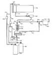
- FIG. 1is a diagram of a system for recycling a work gas for the manufacture of CIGS photovoltaic device according to an embodiment of the present invention.
- the system 1000is associated with a process furnace or thermal reactor 100 that is configured to perform thermal reactive treatment of thin-film devices under a gaseous environment within the furnace.
- the thermal reactor 100is applied to treat thin-film photovoltaic devices using a process gas 101 comprising a mixture of a work gas and one or more carrier gases.
- embodiments of the present inventionare applied to treat a thin-film device comprising a precursor material made by copper and indium (or gallium) species.
- the work gasincludes at least a selenide gas (and also may include sulfide gas) although other types of work gas may be used depending on the applications.
- the carrier gasincludes typically inert gas, for example, nitrogen gas, argon gas, or helium gas, depending on applications.
- the system 1000is configured to recycle the work gas each time after a treatment process following a predetermined thermal profile designed for the thermal reactor 100 .
- the selenium element in the work gas used in the above exampleis a relative expensive material ingredient for forming a thin-film photovoltaic absorber.
- the system 1000is configured to perform an integrated operation associated with the thermal reactive treatment process conducted with the thermal reactor 100 .
- the system 1000starts to operate for recycling the work gas within the thermal reactor 100 .
- the system 1000includes a pump module comprising a valve 201 and a pumping unit 200 .
- the pump moduleconnects to the thermal reactor via a pipe 111 to remove the remaining process gas 101 and generate an exhaust flow that is guided out by the pipe 211 .
- the remaining process gas 101 after treating sample devices in the thermal reactor 100contains an unconsumed portion of hydrogen selenide gas, the inert nitrogen gas (used as a carrier gas), and pyrolyzed hydrogen gas (resulted from thermal break-up of hydrogen selenide gas), while a small quantity of elemental Se particles form and is absorbed at a cooled chamber door region of the thermal reactor 100 .
- the system 1000is operated for recycling the unconsumed hydrogen selenide gas in the specific time period.
- after the thermal reactor is pump down itit can be back-filled with another type of process gas comprising hydrogen sulfide gas, instead of hydrogen selenide gas, for additional thermal treatment of the same sample devices.
- the system 1000can be used to recycle hydrogen sulfide gas from the exhaust flow generated by the pump module via pipe 111 and valve 201 .
- the exhaust flowmay contain significant less portion of the work gas (e.g., hydrogen selenide gas, or hydrogen sulfide gas), instead, mainly the air, the one or more carrier gases, and other residue particles.
- the work gas to be recycled(specifically the hydrogen gas) can be characterized by a first boiling temperature that is at least higher than a highest boiling point of any other gases including the one or more carrier gas or other impurity gases.
- the system 1000includes two pathways for the exhaust flow guided in pipe 211 via a valve 202 and valve 203 , respectively.
- the first pathwayguides the exhaust flow directly to a scrubber module 400 .
- the first pathwayincludes a pipe 212 connected to the valve 202 , another valve 202 a disposed between the pipe 212 and another pipe 215 which connects to the scrubber module 400 .
- the first pathwayis used to guide the exhaust flow during the time periods of initial pump down or final purge of the thermal reactor 100 , because there is not much work gas in the furnace for recycling.
- the second pathwayguides the exhaust flow directly to a condenser module 300 .
- the second pathwayincludes a pipe 213 connected the valve 203 to a container 302 .
- the pipe 213is configured to be surrounded by a condenser coil 300 running with a refrigerant fluid so that any gas molecules passed through the pipe 213 are subjected to a designated cooling process.
- the condenser module 300is configured to be set at an operation temperature that is below the first boiling temperature of the work gas but is higher than the highest boiling point of any other gaseous ingredients within the exhaust flow. As the result of the condenser module operation, the work gas is liquefied by the condenser coil 300 and collected as a liquid 321 by the container 302 .
- the other gaseous ingredientsremain in a gas state and are stored at a top portion of the container 302 as an exit gas 322 .
- the exit gasmay still contain a small quantity of the vapor of the liquid 321 .
- a pipe 214is connected to the top portion of the container 302 for guiding the exit gas 322 out.
- the pipe 214is connected to a valve 204 before merging with the pipe 215 that couples directly to the scrubber module 400 for further cleaning the exit gas.
- the hydrogen selenide gasis used as the work gas for reactively treating a copper-indium (and/or gallium) thin-film precursor material pre-formed on a substrate.
- the work gasis properly mixed with one or more carrier gases to form a process gas 101 before filling into the thermal reactor 100 .
- the process gas 101comprises hydrogen selenide gas mixed with pure nitrogen gas in a ratio ranging from 1:4 to 1:12, and preferred to be about 1:10, with a total pressure set at about 650 Torr.
- a chemical reactionoccurs and leads to a break-up of hydrogen selenide molecules so that selenium (Se) species is incorporated into the thin-film precursor material and the hydrogen species forms hydrogen (H 2 ) gas and releases into the gas mixture within the furnace.
- the reaction of Se with copper-indium precursor materialresults to a formation of copper-indium-diselenide (CIS) material.
- the precursor materialalso comprises gallium species and the reaction leads to the formation of copper-indium-gallium-diselenide (CIGS) material.
- CIS materialcopper-indium-gallium-diselenide
- CIGScopper-indium-gallium-diselenide
- Either the CIS material and CIGS materialhas a p-type semiconductor characteristic and forms a photovoltaic absorber of solar cell.
- the process gas 101now comprises remaining portion of hydrogen selenide (H 2 Se) gas, a small quantity of hydrogen H 2 gas released from the break-up of H 2 Se, nitrogen (N 2 ) gas as the carrier gas, and possibly some other impurity gases.
- H 2 Sehydrogen selenide
- N 2nitrogen
- these gaseswill just the ingredients of the exhaust flow out of the pipe 212 generated by the pump module 200 .
- a small quantity of selenium elemental particlesalso exits but they are heavier and likely have been absorbed by the relative cold regions like the cooled furnace door.
- selenium speciesis the resource to be recycled or recovered in terms of H 2 Se gas by the system 1000 .
- H 2 Se gashas a relative higher boiling temperature at ⁇ 41.25° C., compared to the boiling point of other gases in the exhaust flow: H 2 boiling point at ⁇ 252.87° C., N 2 boiling point at ⁇ 195.79° C., or Argon boiling point ⁇ 185.85° C.
- Thisis an advantage taken by the condenser module 300 for separating the hydrogen selenide H 2 Se from other gases in the exhaust flow.
- the condenser module 300By operating the condenser module 300 at a temperature below the boiling point of H 2 Se but above the highest boiling point of other gases (predominantly the nitrogen gas and small quantity of hydrogen gas), the H 2 Se gas can be liquefied while other gases remain as a gas state. As shown in FIG.
- liquid (H 2 Se) 321is retained in a lower part container 302 while other gases 322 occupies upper portion of the container 302 .
- the valve 202is automatically closed and valve 203 opened.
- the valve 204is opened and the valve 202 a is also closed to guide the other gases via the pipe 215 to the scrubber module 400 .
- the operation of the system 1000is synchronized with the timing of performing thermal reactive treatment based on a predetermined temperature profile from ramping up furnace temperature to one or more dwelling stages and cooling down. More detail description about the selenization and sulfurization process following the temperature profile can be found in U.S.
- the reactive thermal treatment processincludes applying hydrogen sulfide H 2 S gas, replacing H 2 Se gas, in one or more process stages.
- H 2 Salso has a relative high boiling point at ⁇ 60.28° C.
- the system 1000can be implemented for recycling H 2 S in a same manner.
- One optionis, if the process involving H 2 S work gas is performed in the same thermal reactor following the process involving H 2 Se work gas, to use the same system 1000 while having it controlled in timing schedule of condenser operation so that two liquefied materials can be properly stored.
- Another optionis, of course, to install a redundant system ( 1000 a ) and operate the two systems separately and independently.
- H 2 Smay not be as valuable as H 2 Se in terms of material cost.
- the scrubber module 400is configured to clean any exhaust flow resulted from the thermal reactor 100 via a first pathway 212 and from the condenser module 300 via a second pathway 214 .
- the work gasfor example hydrogen selenide gas
- the exhaust flow from the thermal reactor 100 that possibly contains any quantity of such toxic ingredientsmust be treated or purified first before releasing to ambient through an exhaust port 402 .
- a wet scrubber moduleis used for cleaning the exhaust flow. Wet scrubbing works via the contact of molecules of exhaust flow or particulate the work gas molecules with a scrubbing solution.
- the solutionmay simply be water or solutions of reagents that specifically target certain compounds.
- the scrubber module 400also is configured to receive gases 322 flowing from the container 302 of the condenser module 300 .
- the gasesmay contain a small quantity of hydrogen selenide vapor although most of it has been retained inside the container in liquid form.
- the valve 203is opened and valve 204 is also opened while the valve 202 a is closed to guide the gases to the scrubber module 400 after passing through the condenser module 300 .
- the system 1000further includes a boiler module 500 coupled to the condenser module via a valve 205 .
- a boiler module 500coupled to the condenser module via a valve 205 .
- the valve 205controls the liquid flow into the boiler module 500 where the liquid is heated above its boiling point to become a vapor 522 .
- the boiler module 500transforms the hydrogen selenide liquid to a hydrogen selenide vapor or gas.
- the system 1000further includes a pipe 511 coupled to the boiler module 500 via a valve 206 for deliver the vapor or gas 522 .
- the vapor 522is a recycled work gas that can be supplied back to the thermal reactor 100 for additional runs of thermal reactive treatment process.
- the recycled vapor 522 guided by the pipe 511is merged with the work gas from nominal supply line 611 which connects to a cylinder 601 of an original work gas supply source designated for the thermal reactor 100 .
- the system 1000can have at least a mass flow controller 801 configured to receive the merged work gas and set a flow rate for delivering the work gas to a gas line 811 .
- the delivered work gaswill first mix with a carrier gas in a gas line 812 independently supplied via a gas line 711 from a carrier gas source 701 .
- the carrier gasis controlled in terms a pressure indicator by another mass flow controller 802 or simply a pressure valve.
- the work gas supplied in gas line 811is controlled to be at 4-12% in total pressure which is set to about 650 torr for the mixture of the work gas and the carrier gas.
- the work gas versus the carrier gasis set to be about 1:10 ratio to form the process gas to be used to fill the furnace or thermal reactor with the set pressure of about 650 ton.
- a pressure release valve 207is used to keep the pressure within the furnace 100 at approximately 650 torr.
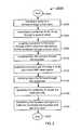
- FIG. 2is a diagram illustrating a method for recycling a work gas for treating thin-film CGIS photovoltaic device according to an embodiment of the present invention. As shown in FIG. 2 , the method includes:
- the method 2000begins at start, step 2020 .
- the user of the methodbegins at a furnace or a thermal reactor, such as the one noted above.
- the thermal reactorcan be maintained at about room temperature and atmosphere before proceeding with the present method.
- a plurality of substratesis transferred into the thermal reactor, step 2020 , to be treated by a work gas in a thermal reactive process.
- Each of the plurality of substratescan include a precursor material to be reacted with at least one target element provided by the work gas.
- the precursor materialis a thin-film comprising several material species separately or commonly deposited over the substrates before loaded into the thermal reactor.
- the plurality of substratescan be 40 or more individual substrates, each having a dimension of 65 cm to 165 cm or smaller. But it is understood that other dimensions are possible.
- each of the substratesis a planar shaped glass plate maintained substantially free from warp or damage.
- the precursor materialis a mixture or alloy with a predetermined stoichiometry of copper species, indium species, and/or gallium species, and doped with sodium species.
- the thermal reactive process using the work gasis intended to conduct at an elevated temperature above 425° C. to nearly 525° C. for transforming the precursor material into a thin-film photovoltaic absorber material.
- the thermal reactive processis a selenization process as the work gas contains selenium species for reacting with the copper-based precursor material.
- the selenium speciesmay come from gaseous elemental selenium vapor or extracted a selenide gas such as hydrogen selenide gas.
- the absorber to be formedwill be a thin-film selenide material.
- another thermal reactive process followed the selenization processis a sulfurization process as the work gas is replaced by hydrogen sulfide gas, after a purge of hydrogen selenide gas, for further incorporating sulfur species into the thin-film selenide material.
- a pump or pump systemis coupled to the thermal reactor or furnace via a first valve in step 2040 .
- the pumpis operated to create or maintain a vacuum state for the furnace at several process stages.
- the pumpat least is configured to conduct operation during several process stages: 1) an initial pumping down, 2) a purge of used process gas after finishing one process run (with one type of work gas), and 3) a final purge of process gas after all processes.
- stage 1) and 3the pump system is able to create an exhaust flow out of the furnace which contains substantially insignificant quantity of the work gas.
- the pump systemis create another exhaust flow that contains substantially significant quantity of the work gas among other carrier gas or impurities.
- a condenseris connected to the pump system through a second valve in step 2060 .
- the condenseris configured to recycle one or more target species from an exhaust flow generated by the pump system.
- the pump systemis operating at a stage 2) above for purging the used process gas after finishing one process run. Within the used process gas there are substantial portion of un-consumed work gas as a recycling target species.
- the condenseris utilizing a relative high boiling point of the target gas species compared to the rest gas species among the used process gas to separate the target species by converting it to a liquid while keeping the rest gas species in a gas state, thereby recollecting the target gas species.
- the condenserincludes a condenser coil with running refrigerant fluid to surround a tube or pipe with the exhaust flow passing by and also includes a container for retaining the liquefied target work gas while delivering the remaining species in gas state as an exit gas flow.
- the exit flowincludes mainly the rest gas species with a substantially small quantity of the target gas species.
- a scrubber moduleis connected to the pump system via at least a third valve and alternatively connected to the condenser via a fourth valve in step 2080 .
- the scrubber moduleincludes a first operation mode configured to receive the exhaust flow directly from the pump system and to treat the exhaust flow before releasing to ambient.
- the scrubber moduleis to clean toxic species in the exhaust flow which mainly comes from the work gas or residue gas released during the chemical reaction between the work gas and sample materials inside the thermal reactor.
- the second valve and the fourth valveare closed and the third valve is opened.
- the scrubber modulecan be a wet scrubber module or a dry scrubber module for cleaning the toxic elements with efficiency and completeness.
- the scrubber moduleincludes a second operation mode configured to receive the exit gas flow from the condenser and still to clean any toxic species therein. At the second operation mode, the second valve and the fourth valve are opened and the third valve is closed.
- step 2100An initial pumping down operation of the furnace is carried out through the pump and the scrubber, in step 2100 .
- the third valvewill be opened to allow the exhaust flow directly into the scrubber from the pump system.
- This step 2100creates a vacuum environment inside the furnace ready for filling a process gas.
- a process gas including a work gas mixed with carrier gasesis supplied into the furnace for treating a sample material, in step 2120 .
- the process gasis premixed with a work gas and one or more carrier gases with a predetermined ratio range.
- the mixtureis monitored by the gas pressure.
- the work gasis hydrogen selenide gas filled in with a partial pressure of about 65 ton.
- the work gasis delivered controllably by a mass flow controller in terms of a set flow rate.
- the work gasis mixed with a pure nitrogen gas so that the total pressure inside the furnace is about 650 torr.
- the work gas and the carrier gashas a mixing ratio ranging from 1:4 to 1:12, while preferred ratio at 1:10.
- the furnace temperaturechanges and so does the pressure.
- the mass flow controller or a pressure valveis used to adjust the flow of the work gas supply.
- the hydrogen selenide gasis supplied as a work gas for specifically treating a copper-based precursor sample material for forming a semiconductor photovoltaic absorber.
- the furnacethen will be heated following a predetermined temperature profile including one or more temperature ramping stages and one or more process dwelling stages. During the whole process stages, the process gas is evolving as work gas element is consumed to be incorporated into the precursor sample material, or residue gas is released into the furnace due to the thermal reaction, or new gas is formed from thermal pyrolyzed molecules of the work gas.
- a new process gasmay include another work gas mixed with the carrier gas.
- the furnaceis pumped down by the pump system to send an exhaust flow through the condenser, in step 2140 .
- the furnaceis operating in a time period that needs to purge out the used process gas therein and the condenser is in an operation mode for recycling the target gas species within the purged exhaust flow.
- the second valveis opened to allow the exhaust flow to pass through the condenser coil where the operating temperature has been set at a value that is lower than the boiling point of a target gas species but higher than rest gas species.
- the purged exhaust flowis a used process gas after a thermal reactive process including unconsumed work gas, carrier gas, and any released gas during the thermal reaction as a by-product.
- the work gasis hydrogen selenide gas intended for reactively treating a copper-indium based thin-film precursor material at an elevated temperature for forming a thin-film photovoltaic absorber.
- the thermal reactive treatmentabout 15% of hydrogen selenide gas is consumed and a small quantity of hydrogen selenide is thermally pyrolyzed into elemental Se with H 2 gas as a by-product released into the process gas mixture.
- the rest 80+% hydrogen selenideremains in the used process gas including also 90% nitrogen gas as carrier gas.
- step 2160the method operates the condenser to liquefy substantially only the work gas out of the purged exhaust flow.
- the condenser coil operated at a temperature below the boiling point of the target speciesi.e., hydrogen selenide
- hydrogen selenide gasis then liquefied into a H 2 Se liquid while rest species including mainly H 2 gas and N 2 gas (either of which has a much lower boiling point than H 2 Se) still is in a gas phase, physically being separated from the H 2 Se liquid.
- the thermal reactormay be in different operation stage where the process gas is replaced by a new work gas or there may be different type of gas by-product after a different thermal reactive process, but one or more embodiments described above can be still applied.
- the liquefied work gasis transferred to a boiler to be converted back to a vapor, in step 2180 .
- the boilerhas an input port coupled to the container of the condenser via a valve.
- the liquid target species stored in the containercan be controllably sent to the boiler where the liquid is heated to transform the recycled liquid back to its vapor form.
- the boileralso includes a output port for deliver the vapor species.
- the H 2 Se liquidflows from the condenser container to the boiler and is turned into H 2 Se vapor. Through the output port the H 2 Se vapor or gas is delivered out through a gas line.
- the gas linecan be directly led back to the thermal reactor to complete the recycling process.
- the gas line of the H 2 Se vaporis first merged with another gas line originated from the H 2 Se gas supply cylinder. Then a mass flow controller is added to deliver the merged H 2 Se gas with a steady flow rate.
- the H 2 Se gas flowis determined based on the total pressure required for the thermal reactive treatment in the furnace.
- the work gasis provided as a just about 10% part of a process gas and the rest 90% part provided by an inert carrier gas.
- the hydrogen selenide gasis mixed with nitrogen gas and the combined process gas is filled the furnace with a pressure set at approximately 650 torr.
- the thermal reactive processmay be extended to another process stage where the work gas can be replaced by a new work gas
- the recycling operationcan be carried by using a switch valve to link to a redundant condenser and boiler combination to the pump output port. Therefore, the new work gas can be recycled although the condenser or boiler may be adjusted their operation conditions accordingly.
- the methodincludes a stop operation.
- a cooling stagemay start and the furnace final purge also starts.
- the recycling operationcan be stopped and the valve towards the scrubber module is opened to send the final purged exhaust flow directly for pollution control and release to ambient.
Landscapes
- Chemical & Material Sciences (AREA)
- Organic Chemistry (AREA)
- Engineering & Computer Science (AREA)
- Chemical Kinetics & Catalysis (AREA)
- Inorganic Chemistry (AREA)
- Oil, Petroleum & Natural Gas (AREA)
- General Chemical & Material Sciences (AREA)
- Analytical Chemistry (AREA)
- Health & Medical Sciences (AREA)
- General Health & Medical Sciences (AREA)
- Combustion & Propulsion (AREA)
- Life Sciences & Earth Sciences (AREA)
- Sustainable Development (AREA)
- Biomedical Technology (AREA)
- Environmental & Geological Engineering (AREA)
- Treating Waste Gases (AREA)
- Photovoltaic Devices (AREA)
Abstract
Description
Claims (13)
Priority Applications (2)
| Application Number | Priority Date | Filing Date | Title |
|---|---|---|---|
| US13/343,473US8728200B1 (en) | 2011-01-14 | 2012-01-04 | Method and system for recycling processing gas for selenization of thin film photovoltaic materials |
| US14/282,925US9084969B1 (en) | 2011-01-14 | 2014-05-20 | Method and system for recycling processing gas for selenization of thin film photovoltaic materials |
Applications Claiming Priority (2)
| Application Number | Priority Date | Filing Date | Title |
|---|---|---|---|
| US201161432869P | 2011-01-14 | 2011-01-14 | |
| US13/343,473US8728200B1 (en) | 2011-01-14 | 2012-01-04 | Method and system for recycling processing gas for selenization of thin film photovoltaic materials |
Related Child Applications (1)
| Application Number | Title | Priority Date | Filing Date |
|---|---|---|---|
| US14/282,925ContinuationUS9084969B1 (en) | 2011-01-14 | 2014-05-20 | Method and system for recycling processing gas for selenization of thin film photovoltaic materials |
Publications (1)
| Publication Number | Publication Date |
|---|---|
| US8728200B1true US8728200B1 (en) | 2014-05-20 |
Family
ID=50692189
Family Applications (2)
| Application Number | Title | Priority Date | Filing Date |
|---|---|---|---|
| US13/343,473Expired - Fee RelatedUS8728200B1 (en) | 2011-01-14 | 2012-01-04 | Method and system for recycling processing gas for selenization of thin film photovoltaic materials |
| US14/282,925Expired - Fee RelatedUS9084969B1 (en) | 2011-01-14 | 2014-05-20 | Method and system for recycling processing gas for selenization of thin film photovoltaic materials |
Family Applications After (1)
| Application Number | Title | Priority Date | Filing Date |
|---|---|---|---|
| US14/282,925Expired - Fee RelatedUS9084969B1 (en) | 2011-01-14 | 2014-05-20 | Method and system for recycling processing gas for selenization of thin film photovoltaic materials |
Country Status (1)
| Country | Link |
|---|---|
| US (2) | US8728200B1 (en) |
Cited By (3)
| Publication number | Priority date | Publication date | Assignee | Title |
|---|---|---|---|---|
| US20140264988A1 (en)* | 2013-03-15 | 2014-09-18 | The Government Of The United States Of America, As Represented By The Secretary Of The Navy | Photovoltaic sputtering targets fabricated from reclaimed materials |
| WO2016032046A1 (en)* | 2014-08-29 | 2016-03-03 | 에스엔유 프리시젼 주식회사 | Cigs heat treatment selenium supply device and supply method |
| EP3736355A1 (en)* | 2019-05-06 | 2020-11-11 | (CNBM) Bengbu Design & Research Institute for Glass Industry Co., Ltd. | Method and device for producing a bridging semiconductor containing chalcogen |
Citations (238)
| Publication number | Priority date | Publication date | Assignee | Title |
|---|---|---|---|---|
| US3520732A (en) | 1965-10-22 | 1970-07-14 | Matsushita Electric Industrial Co Ltd | Photovoltaic cell and process of preparation of same |
| US3828722A (en) | 1970-05-01 | 1974-08-13 | Cogar Corp | Apparatus for producing ion-free insulating layers |
| US3975211A (en) | 1975-03-28 | 1976-08-17 | Westinghouse Electric Corporation | Solar cells and method for making same |
| US4062038A (en) | 1976-01-28 | 1977-12-06 | International Business Machines Corporation | Radiation responsive device |
| US4263336A (en) | 1979-11-23 | 1981-04-21 | Motorola, Inc. | Reduced pressure induction heated reactor and method |
| US4332974A (en) | 1979-06-28 | 1982-06-01 | Chevron Research Company | Multilayer photovoltaic cell |
| US4335266A (en) | 1980-12-31 | 1982-06-15 | The Boeing Company | Methods for forming thin-film heterojunction solar cells from I-III-VI.sub.2 |
| DE3314197A1 (en) | 1982-04-28 | 1983-11-03 | Energy Conversion Devices, Inc., 48084 Troy, Mich. | P-CONDUCTING AMORPHOUS SILICON ALLOY WITH A LARGE BAND GAP AND MANUFACTURING PROCESS THEREFOR |
| US4441113A (en) | 1981-02-13 | 1984-04-03 | Energy Conversion Devices, Inc. | P-Type semiconductor material having a wide band gap |
| US4442310A (en) | 1982-07-15 | 1984-04-10 | Rca Corporation | Photodetector having enhanced back reflection |
| US4461922A (en) | 1983-02-14 | 1984-07-24 | Atlantic Richfield Company | Solar cell module |
| US4465575A (en) | 1981-09-21 | 1984-08-14 | Atlantic Richfield Company | Method for forming photovoltaic cells employing multinary semiconductor films |
| US4471155A (en) | 1983-04-15 | 1984-09-11 | Energy Conversion Devices, Inc. | Narrow band gap photovoltaic devices with enhanced open circuit voltage |
| US4499658A (en) | 1983-09-06 | 1985-02-19 | Atlantic Richfield Company | Solar cell laminates |
| US4507181A (en) | 1984-02-17 | 1985-03-26 | Energy Conversion Devices, Inc. | Method of electro-coating a semiconductor device |
| US4517403A (en) | 1983-05-16 | 1985-05-14 | Atlantic Richfield Company | Series connected solar cells and method of formation |
| US4518855A (en) | 1982-09-30 | 1985-05-21 | Spring-Mornne, Inc. | Method and apparatus for statically aligning shafts and monitoring shaft alignment |
| US4532372A (en) | 1983-12-23 | 1985-07-30 | Energy Conversion Devices, Inc. | Barrier layer for photovoltaic devices |
| US4542255A (en) | 1984-01-03 | 1985-09-17 | Atlantic Richfield Company | Gridded thin film solar cell |
| US4581108A (en) | 1984-01-06 | 1986-04-08 | Atlantic Richfield Company | Process of forming a compound semiconductive material |
| US4589194A (en) | 1983-12-29 | 1986-05-20 | Atlantic Richfield Company | Ultrasonic scribing of thin film solar cells |
| US4598306A (en) | 1983-07-28 | 1986-07-01 | Energy Conversion Devices, Inc. | Barrier layer for photovoltaic devices |
| US4599154A (en) | 1985-03-15 | 1986-07-08 | Atlantic Richfield Company | Electrically enhanced liquid jet processing |
| US4611091A (en) | 1984-12-06 | 1986-09-09 | Atlantic Richfield Company | CuInSe2 thin film solar cell with thin CdS and transparent window layer |
| US4623601A (en) | 1985-06-04 | 1986-11-18 | Atlantic Richfield Company | Photoconductive device containing zinc oxide transparent conductive layer |
| US4625070A (en) | 1985-08-30 | 1986-11-25 | Atlantic Richfield Company | Laminated thin film solar module |
| US4638111A (en) | 1985-06-04 | 1987-01-20 | Atlantic Richfield Company | Thin film solar cell module |
| US4661370A (en) | 1984-02-08 | 1987-04-28 | Atlantic Richfield Company | Electric discharge processing of thin films |
| US4663495A (en) | 1985-06-04 | 1987-05-05 | Atlantic Richfield Company | Transparent photovoltaic module |
| US4705912A (en) | 1985-09-27 | 1987-11-10 | Sanyo Electric Co., Ltd. | Photovoltaic device |
| US4724011A (en) | 1983-05-16 | 1988-02-09 | Atlantic Richfield Company | Solar cell interconnection by discrete conductive regions |
| US4727047A (en) | 1980-04-10 | 1988-02-23 | Massachusetts Institute Of Technology | Method of producing sheets of crystalline material |
| US4751149A (en) | 1985-06-04 | 1988-06-14 | Atlantic Richfield Company | Chemical vapor deposition of zinc oxide films and products |
| US4775425A (en) | 1987-07-27 | 1988-10-04 | Energy Conversion Devices, Inc. | P and n-type microcrystalline semiconductor alloy material including band gap widening elements, devices utilizing same |
| US4793283A (en) | 1987-12-10 | 1988-12-27 | Sarkozy Robert F | Apparatus for chemical vapor deposition with clean effluent and improved product yield |
| US4798660A (en) | 1985-07-16 | 1989-01-17 | Atlantic Richfield Company | Method for forming Cu In Se2 films |
| US4816082A (en) | 1987-08-19 | 1989-03-28 | Energy Conversion Devices, Inc. | Thin film solar cell including a spatially modulated intrinsic layer |
| US4865999A (en) | 1987-07-08 | 1989-09-12 | Glasstech Solar, Inc. | Solar cell fabrication method |
| US4873118A (en) | 1988-11-18 | 1989-10-10 | Atlantic Richfield Company | Oxygen glow treating of ZnO electrode for thin film silicon solar cell |
| US4915745A (en) | 1988-09-22 | 1990-04-10 | Atlantic Richfield Company | Thin film solar cell and method of making |
| US4950615A (en) | 1989-02-06 | 1990-08-21 | International Solar Electric Technology, Inc. | Method and making group IIB metal - telluride films and solar cells |
| US4968354A (en) | 1987-11-09 | 1990-11-06 | Fuji Electric Co., Ltd. | Thin film solar cell array |
| US4996108A (en) | 1989-01-17 | 1991-02-26 | Simon Fraser University | Sheets of transition metal dichalcogenides |
| US5008062A (en) | 1988-01-20 | 1991-04-16 | Siemens Solar Industries, L.P. | Method of fabricating photovoltaic module |
| US5011565A (en) | 1989-12-06 | 1991-04-30 | Mobil Solar Energy Corporation | Dotted contact solar cell and method of making same |
| US5028274A (en) | 1989-06-07 | 1991-07-02 | International Solar Electric Technology, Inc. | Group I-III-VI2 semiconductor films for solar cell application |
| US5039353A (en) | 1989-04-27 | 1991-08-13 | Societe Dite: Solems (Societe Anonyme) | Process for improving the spectral response of a photoconductive structure, and improved solar cell and photoreceptive structure |
| US5045409A (en) | 1987-11-27 | 1991-09-03 | Atlantic Richfield Company | Process for making thin film solar cell |
| US5069727A (en) | 1989-09-06 | 1991-12-03 | Sanyo Electric Co., Ltd. | Flexible photovoltaic device and manufacturing method thereof |
| US5078803A (en) | 1989-09-22 | 1992-01-07 | Siemens Solar Industries L.P. | Solar cells incorporating transparent electrodes comprising hazy zinc oxide |
| US5125984A (en) | 1990-05-31 | 1992-06-30 | Siemens Aktiengesellschaft | Induced junction chalcopyrite solar cell |
| US5133809A (en) | 1989-10-07 | 1992-07-28 | Showa Shell Sekiyu K.K. | Photovoltaic device and process for manufacturing the same |
| US5137835A (en) | 1990-07-24 | 1992-08-11 | Siemens Aktiengesellschaft | Method for manufacturing a chalcopyrite solar cell |
| US5154777A (en) | 1990-02-26 | 1992-10-13 | Mcdonnell Douglas Corporation | Advanced survivable space solar power system |
| US5180686A (en) | 1988-10-31 | 1993-01-19 | Energy Conversion Devices, Inc. | Method for continuously deposting a transparent oxide material by chemical pyrolysis |
| US5211824A (en) | 1991-10-31 | 1993-05-18 | Siemens Solar Industries L.P. | Method and apparatus for sputtering of a liquid |
| US5217564A (en) | 1980-04-10 | 1993-06-08 | Massachusetts Institute Of Technology | Method of producing sheets of crystalline material and devices made therefrom |
| US5231047A (en) | 1991-12-19 | 1993-07-27 | Energy Conversion Devices, Inc. | High quality photovoltaic semiconductor material and laser ablation method of fabrication same |
| US5248345A (en) | 1990-10-17 | 1993-09-28 | Showa Shell Sekiyu K.K. | Integrated photovoltaic device |
| US5259883A (en) | 1988-02-16 | 1993-11-09 | Kabushiki Kaisha Toshiba | Method of thermally processing semiconductor wafers and an apparatus therefor |
| US5261968A (en) | 1992-01-13 | 1993-11-16 | Photon Energy, Inc. | Photovoltaic cell and method |
| US5298086A (en) | 1992-05-15 | 1994-03-29 | United Solar Systems Corporation | Method for the manufacture of improved efficiency tandem photovoltaic device and device manufactured thereby |
| US5336623A (en) | 1992-03-02 | 1994-08-09 | Showa Shell Sekiyu K.K. | Process for producing integrated solar cell |
| US5346853A (en) | 1992-06-29 | 1994-09-13 | United Solar Systems Corporation | Microwave energized deposition process with substrate temperature control for the fabrication of P-I-N photovoltaic devices |
| US5397401A (en) | 1992-06-29 | 1995-03-14 | Canon Kabushiki Kaisha | Semiconductor apparatus covered with a sealing resin composition |
| US5399504A (en) | 1991-05-08 | 1995-03-21 | Fuji Electric Corporate Research & Development Ltd. | Method of manufacturing CuInSe2 thin film solar cell |
| US5436204A (en) | 1993-04-12 | 1995-07-25 | Midwest Research Institute | Recrystallization method to selenization of thin-film Cu(In,Ga)Se2 for semiconductor device applications |
| US5445847A (en) | 1992-05-19 | 1995-08-29 | Matsushita Electric Industrial Co., Ltd. | Method for preparing chalcopyrite-type compound |
| US5474939A (en) | 1992-12-30 | 1995-12-12 | Siemens Solar Industries International | Method of making thin film heterojunction solar cell |
| US5501744A (en) | 1992-01-13 | 1996-03-26 | Photon Energy, Inc. | Photovoltaic cell having a p-type polycrystalline layer with large crystals |
| US5512107A (en) | 1992-03-19 | 1996-04-30 | Siemens Solar Gmbh | Environmentally stable thin-film solar module |
| US5528397A (en) | 1991-12-03 | 1996-06-18 | Kopin Corporation | Single crystal silicon transistors for display panels |
| US5536333A (en) | 1992-05-12 | 1996-07-16 | Solar Cells, Inc. | Process for making photovoltaic devices and resultant product |
| US5578103A (en) | 1994-08-17 | 1996-11-26 | Corning Incorporated | Alkali metal ion migration control |
| US5578503A (en) | 1992-09-22 | 1996-11-26 | Siemens Aktiengesellschaft | Rapid process for producing a chalcopyrite semiconductor on a substrate |
| US5622634A (en) | 1993-12-17 | 1997-04-22 | Canon Kabushiki Kaisha | Method of manufacturing electron-emitting device, electron source and image-forming apparatus |
| US5626688A (en) | 1994-12-01 | 1997-05-06 | Siemens Aktiengesellschaft | Solar cell with chalcopyrite absorber layer |
| US5665175A (en) | 1990-05-30 | 1997-09-09 | Safir; Yakov | Bifacial solar cell |
| US5676766A (en) | 1993-09-30 | 1997-10-14 | Siemens Aktiengesellschaft | Solar cell having a chalcopyrite absorber layer |
| US5726065A (en) | 1995-02-21 | 1998-03-10 | Imec Vzw | Method of preparing solar cell front contacts |
| US5738731A (en) | 1993-11-19 | 1998-04-14 | Mega Chips Corporation | Photovoltaic device |
| US5779877A (en)* | 1997-05-12 | 1998-07-14 | Drinkard Metalox, Inc. | Recycling of CIS photovoltaic waste |
| US5858819A (en) | 1994-06-15 | 1999-01-12 | Seiko Epson Corporation | Fabrication method for a thin film semiconductor device, the thin film semiconductor device itself, liquid crystal display, and electronic device |
| US5868869A (en) | 1995-06-07 | 1999-02-09 | Photon Energy, Inc. | Thin film photovoltaic device and process of manufacture |
| US5977476A (en) | 1996-10-16 | 1999-11-02 | United Solar Systems Corporation | High efficiency photovoltaic device |
| US5981868A (en) | 1996-10-25 | 1999-11-09 | Showa Shell Sekiyu K.K. | Thin-film solar cell comprising thin-film light absorbing layer of chalcopyrite multi-element compound semiconductor |
| US5985691A (en) | 1997-05-16 | 1999-11-16 | International Solar Electric Technology, Inc. | Method of making compound semiconductor films and making related electronic devices |
| US6040521A (en) | 1996-11-08 | 2000-03-21 | Showa Shell Sekiyu K.K. | N-type window layer for a thin film solar cell and method of making |
| US6048442A (en) | 1996-10-25 | 2000-04-11 | Showa Shell Sekiyu K.K. | Method for producing thin-film solar cell and equipment for producing the same |
| JP2000173969A (en) | 1998-12-03 | 2000-06-23 | Canon Inc | Rinse method and photovoltaic device |
| JP2000219512A (en) | 1998-11-24 | 2000-08-08 | Canon Inc | Method for manufacturing zinc oxide thin film, method for manufacturing photovoltaic device using the same, and photovoltaic device |
| US6107562A (en) | 1998-03-24 | 2000-08-22 | Matsushita Electric Industrial Co., Ltd. | Semiconductor thin film, method for manufacturing the same, and solar cell using the same |
| US6127202A (en) | 1998-07-02 | 2000-10-03 | International Solar Electronic Technology, Inc. | Oxide-based method of making compound semiconductor films and making related electronic devices |
| US6160215A (en) | 1999-03-26 | 2000-12-12 | Curtin; Lawrence F. | Method of making photovoltaic device |
| US6166319A (en) | 1997-08-01 | 2000-12-26 | Canon Kabushiki Kaisha | Multi-junction photovoltaic device with microcrystalline I-layer |
| US6172297B1 (en) | 1997-09-23 | 2001-01-09 | Institut Fur Solarenergieforschung Gmbh | Solar cell and method for fabrication of a solar cell |
| US6258620B1 (en) | 1997-10-15 | 2001-07-10 | University Of South Florida | Method of manufacturing CIGS photovoltaic devices |
| WO2001057932A1 (en) | 2000-02-07 | 2001-08-09 | Cis Solartechnik Gmbh | Flexible metal substrate for cis solar cells, and method for producing the same |
| US6294274B1 (en) | 1998-11-16 | 2001-09-25 | Tdk Corporation | Oxide thin film |
| US6307148B1 (en) | 1999-03-29 | 2001-10-23 | Shinko Electric Industries Co., Ltd. | Compound semiconductor solar cell and production method thereof |
| US6323417B1 (en) | 1998-09-29 | 2001-11-27 | Lockheed Martin Corporation | Method of making I-III-VI semiconductor materials for use in photovoltaic cells |
| US6328871B1 (en) | 1999-08-16 | 2001-12-11 | Applied Materials, Inc. | Barrier layer for electroplating processes |
| US20020004302A1 (en) | 1995-09-14 | 2002-01-10 | Yoshihiko Fukumoto | Method for fabricating semiconductor device |
| US20020002992A1 (en) | 1998-06-30 | 2002-01-10 | Toshimitsu Kariya | Photovoltaic element |
| US6361718B1 (en) | 1998-02-05 | 2002-03-26 | Nippon Sheet Glass Co., Ltd. | Article having uneven surface, production process for the article, and composition for the process |
| US6372538B1 (en) | 2000-03-16 | 2002-04-16 | University Of Delaware | Fabrication of thin-film, flexible photovoltaic module |
| US20020061361A1 (en) | 2000-09-06 | 2002-05-23 | Hiroki Nakahara | Method and apparatus for fabricating electro-optical device and method and apparatus for fabricating liquid crystal panel |
| US20020063065A1 (en) | 2000-09-19 | 2002-05-30 | Yuichi Sonoda | Method of forming zinc oxide film and process for producing photovoltaic device using it |
| JP2002167695A (en) | 2000-09-19 | 2002-06-11 | Canon Inc | Method for forming zinc oxide film and method for manufacturing photovoltaic element using the same |
| US6423565B1 (en) | 2000-05-30 | 2002-07-23 | Kurt L. Barth | Apparatus and processes for the massproduction of photovotaic modules |
| DE10104726A1 (en) | 2001-02-02 | 2002-08-08 | Siemens Solar Gmbh | Process for structuring an oxide layer applied to a carrier material |
| JP2002270871A (en) | 2001-03-12 | 2002-09-20 | Canon Inc | Semiconductor element and method of forming silicon-based thin film |
| US20030075717A1 (en) | 2001-03-12 | 2003-04-24 | Takaharu Kondo | Semiconductor element, and method of forming silicon-based film |
| US20030089899A1 (en) | 2000-08-22 | 2003-05-15 | Lieber Charles M. | Nanoscale wires and related devices |
| US20030188777A1 (en) | 2002-01-25 | 2003-10-09 | Konarka Technologies, Inc. | Co-sensitizers for dye sensitized solar cells |
| US6632113B1 (en) | 1998-09-09 | 2003-10-14 | Canon Kabushiki Kaisha | Image display apparatus, disassembly processing method therefor, and component recovery method |
| US6635307B2 (en) | 2001-12-12 | 2003-10-21 | Nanotek Instruments, Inc. | Manufacturing method for thin-film solar cells |
| US6653701B1 (en) | 1999-03-09 | 2003-11-25 | Fuji Xerox Co., Ltd. | Semiconductor device and production method thereof |
| US20030230338A1 (en) | 2002-06-17 | 2003-12-18 | Shalini Menezes | Thin film solar cell configuration and fabrication method |
| US6667492B1 (en) | 1997-11-10 | 2003-12-23 | Don L. Kendall | Quantum ridges and tips |
| US6690041B2 (en) | 2002-05-14 | 2004-02-10 | Global Solar Energy, Inc. | Monolithically integrated diodes in thin-film photovoltaic devices |
| US6692820B2 (en) | 1998-08-19 | 2004-02-17 | The Trustees Of Princeton University | Organic photosensitive optoelectronic device with a charge blocking layer |
| US20040063320A1 (en) | 2002-09-30 | 2004-04-01 | Hollars Dennis R. | Manufacturing apparatus and method for large-scale production of thin-film solar cells |
| US20040084080A1 (en) | 2002-06-22 | 2004-05-06 | Nanosolar, Inc. | Optoelectronic device and fabrication method |
| US20040095658A1 (en) | 2002-09-05 | 2004-05-20 | Nanosys, Inc. | Nanocomposites |
| US6784492B1 (en) | 1991-03-18 | 2004-08-31 | Canon Kabushiki Kaisha | Semiconductor device including a gate-insulated transistor |
| US20040187917A1 (en) | 2003-03-29 | 2004-09-30 | Nanosolar, Inc. | Transparent electrode, optoelectronic apparatus and devices |
| JP2004332043A (en) | 2003-05-07 | 2004-11-25 | Canon Inc | Method and apparatus for forming zinc oxide thin film, and method for forming photovoltaic element |
| US20040245912A1 (en) | 2003-04-01 | 2004-12-09 | Innovalight | Phosphor materials and illumination devices made therefrom |
| US20040252488A1 (en) | 2003-04-01 | 2004-12-16 | Innovalight | Light-emitting ceiling tile |
| US20040256001A1 (en) | 2002-12-17 | 2004-12-23 | General Electric Company | Photovoltaic cell using stable cu2o nanocrystals and conductive polymers |
| WO2005011002A1 (en) | 2003-07-24 | 2005-02-03 | Kaneka Corporation | Silicon based thin film solar cell |
| US6852920B2 (en) | 2002-06-22 | 2005-02-08 | Nanosolar, Inc. | Nano-architected/assembled solar electricity cell |
| US20050074915A1 (en) | 2001-07-13 | 2005-04-07 | Tuttle John R. | Thin-film solar cell fabricated on a flexible metallic substrate |
| US6878871B2 (en) | 2002-09-05 | 2005-04-12 | Nanosys, Inc. | Nanostructure and nanocomposite based compositions and photovoltaic devices |
| US20050098205A1 (en) | 2003-05-21 | 2005-05-12 | Nanosolar, Inc. | Photovoltaic devices fabricated from insulating nanostructured template |
| US20050164432A1 (en) | 2000-08-22 | 2005-07-28 | President And Fellows Of Harvard College | Doped elongated semiconductors, growing such semiconductors, devices including such semiconductors and fabricating such devices |
| US20050194036A1 (en) | 2004-03-01 | 2005-09-08 | Basol Bulent M. | Low cost and high throughput deposition methods and apparatus for high density semiconductor film growth |
| JP2005311292A (en) | 2004-03-25 | 2005-11-04 | Kaneka Corp | Substrate for thin film solar cell, manufacturing method therefor, and thin film solar cell using the same |
| US20050287717A1 (en) | 2004-06-08 | 2005-12-29 | Nanosys, Inc. | Methods and devices for forming nanostructure monolayers and devices including such monolayers |
| US20060034065A1 (en) | 2004-08-10 | 2006-02-16 | Innovalight, Inc. | Light strips for lighting and backlighting applications |
| US20060040103A1 (en) | 2004-06-08 | 2006-02-23 | Nanosys, Inc. | Post-deposition encapsulation of nanostructures: compositions, devices and systems incorporating same |
| US20060051505A1 (en) | 2004-06-18 | 2006-03-09 | Uwe Kortshagen | Process and apparatus for forming nanoparticles using radiofrequency plasmas |
| US20060096635A1 (en) | 2004-11-10 | 2006-05-11 | Daystar Technologies, Inc. | Pallet based system for forming thin-film solar cells |
| US20060096537A1 (en) | 2004-11-10 | 2006-05-11 | Daystar Technologies, Inc. | Method and apparatus for forming a thin-film solar cell using a continuous process |
| US20060096536A1 (en) | 2004-11-10 | 2006-05-11 | Daystar Technologies, Inc. | Pressure control system in a photovoltaic substrate deposition apparatus |
| US20060112983A1 (en) | 2004-11-17 | 2006-06-01 | Nanosys, Inc. | Photoactive devices and components with enhanced efficiency |
| US20060130890A1 (en) | 2004-12-20 | 2006-06-22 | Palo Alto Research Center Incorporated. | Heterojunction photovoltaic cell |
| US20060160261A1 (en) | 2005-01-20 | 2006-07-20 | Nanosolar, Inc. | Series interconnected optoelectronic device module assembly |
| US20060173113A1 (en) | 2005-02-01 | 2006-08-03 | Nippon Paint Co., Ltd. | Powder coating composition and coating method of aluminum wheel |
| US20060174932A1 (en) | 2003-07-14 | 2006-08-10 | Hiroki Usui | Electrolyte compositon, photoelectric converter and dye-sensitized solar cell using same |
| US20060219547A1 (en) | 2004-11-10 | 2006-10-05 | Daystar Technologies, Inc. | Vertical production of photovoltaic devices |
| US20060220059A1 (en) | 2003-04-09 | 2006-10-05 | Matsushita Electric Industrial Co., Ltd | Solar cell |
| US20060219288A1 (en) | 2004-11-10 | 2006-10-05 | Daystar Technologies, Inc. | Process and photovoltaic device using an akali-containing layer |
| US7122398B1 (en) | 2004-03-25 | 2006-10-17 | Nanosolar, Inc. | Manufacturing of optoelectronic devices |
| US20060249202A1 (en) | 2004-09-20 | 2006-11-09 | Seunghyup Yoo | Photovoltaic cell |
| WO2006126598A1 (en) | 2005-05-27 | 2006-11-30 | Showa Shell Sekiyu K.K. | Method for continuously depositing high resistance buffer layer/window layer (transparent conductive film) of cis based thin film solar cell and continuous film deposition equipment for carrying out that method |
| US20060267054A1 (en) | 2002-02-05 | 2006-11-30 | Peter Martin | Image sensor with microcrystalline germanium photodiode layer |
| US20070006914A1 (en) | 2004-06-18 | 2007-01-11 | Lee Howard W | Nanostructured materials and photovoltaic devices including nanostructured materials |
| US7179677B2 (en) | 2003-09-03 | 2007-02-20 | Midwest Research Institute | ZnO/Cu(InGa)Se2 solar cells prepared by vapor phase Zn doping |
| WO2007022221A2 (en) | 2005-08-16 | 2007-02-22 | Nanosolar, Inc. | Photovolatic devices with conductive barrier layers and foil substrates |
| US7194197B1 (en) | 2000-03-16 | 2007-03-20 | Global Solar Energy, Inc. | Nozzle-based, vapor-phase, plume delivery structure for use in production of thin-film deposition layer |
| US20070089782A1 (en) | 2003-10-02 | 2007-04-26 | Scheuten Glasgroep | Spherical or grain-shaped semiconductor element for use in solar cells and method for producing the same; method for producing a solar cell comprising said semiconductor element and solar cell |
| US20070116893A1 (en) | 2005-11-18 | 2007-05-24 | Daystar Technologies, Inc. | Low-hydrogen photovoltaic cell |
| US7235736B1 (en) | 2006-03-18 | 2007-06-26 | Solyndra, Inc. | Monolithic integration of cylindrical solar cells |
| US20070151596A1 (en) | 2004-02-20 | 2007-07-05 | Sharp Kabushiki Kaisha | Substrate for photoelectric conversion device, photoelectric conversion device, and stacked photoelectric conversion device |
| WO2007077171A2 (en) | 2005-12-28 | 2007-07-12 | Sulfurcell Solartechnik Gmbh | Method and device for converting metallic precursors into chalcopyrite layers of cigss solar cells |
| US20070163643A1 (en) | 2004-02-19 | 2007-07-19 | Nanosolar, Inc. | High-throughput printing of chalcogen layer and the use of an inter-metallic material |
| US20070169810A1 (en) | 2004-02-19 | 2007-07-26 | Nanosolar, Inc. | High-throughput printing of semiconductor precursor layer by use of chalcogen-containing vapor |
| US7252923B2 (en) | 2001-10-16 | 2007-08-07 | Dai Nippon Printing Co., Ltd. | Methods for producing pattern-forming body |
| US20070193623A1 (en) | 2006-02-22 | 2007-08-23 | Guardian Industries Corp. | Electrode structure for use in electronic device and method of making same |
| US7265037B2 (en) | 2003-06-20 | 2007-09-04 | The Regents Of The University Of California | Nanowire array and nanowire solar cells and methods for forming the same |
| US20070209700A1 (en) | 2004-04-28 | 2007-09-13 | Honda Motor Co., Ltd. | Chalcopyrite Type Solar Cell |
| US20070264488A1 (en) | 2006-05-15 | 2007-11-15 | Stion Corporation | Method and structure for thin film photovoltaic materials using semiconductor materials |
| US20070283998A1 (en) | 2004-12-28 | 2007-12-13 | Showa Shell Sekiyu K.K. | Precursor Film And Method Of Forming The Same |
| US20070289624A1 (en) | 2004-08-09 | 2007-12-20 | Showa Shell Sekiyu K.K. | Cis Compound Semiconductor Thin-Film Solar Cell and Method of Forming Light Absorption Layer of the Solar Cell |
| US20080032044A1 (en) | 2004-12-28 | 2008-02-07 | Showa Shell Sekiyu K.K. | Process For Producing Zno Transparent Conductive Film By Mocvd (Metal-Organic Chemical Vapor Deposition) Method |
| US20080029154A1 (en) | 2006-08-04 | 2008-02-07 | Erel Milshtein | System and method for creating electric isolation between layers comprising solar cells |
| US20080041446A1 (en) | 2006-08-09 | 2008-02-21 | Industrial Technology Research Institute | Dye-sensitized solar cells and method for fabricating same |
| WO2008025326A2 (en) | 2006-09-01 | 2008-03-06 | Cis Solartechnik Gmbh & Co. Kg | Solar cell, method for manufacturing solar cells and electric conductor track |
| US20080057616A1 (en) | 2006-06-12 | 2008-03-06 | Robinson Matthew R | Bandgap grading in thin-film devices via solid group iiia particles |
| US20080092945A1 (en) | 2006-10-24 | 2008-04-24 | Applied Quantum Technology Llc | Semiconductor Grain and Oxide Layer for Photovoltaic Cells |
| US20080092954A1 (en) | 2005-01-12 | 2008-04-24 | In-Solar Tech. Co. Ltd. | Optical Absorber Layers For Solar Cell And Method Of Manufacturing The Same |
| US20080092953A1 (en) | 2006-05-15 | 2008-04-24 | Stion Corporation | Method and structure for thin film photovoltaic materials using bulk semiconductor materials |
| US7364808B2 (en) | 2001-10-19 | 2008-04-29 | Asahi Glass Company, Limited | Substrate with transparent conductive oxide film, process for its production and photoelectric conversion element |
| US20080105294A1 (en) | 2004-12-22 | 2008-05-08 | Showa Shell Sekiyu K.K. | Cis Type Thin-Film Photovoltaic Module, Process for Producing the Photovoltaic Module, and Method of Separating the Module |
| US20080110495A1 (en) | 2004-12-28 | 2008-05-15 | Showa Shell Sekiyu K.K. | Method for Forming Light Absorption Layer of Cis Type Thin-Film Solar Cell |
| US20080121277A1 (en) | 2004-02-19 | 2008-05-29 | Robinson Matthew R | High-throughput printing of semiconductor precursor layer from chalcogenide microflake particles |
| US20080121264A1 (en) | 2006-11-28 | 2008-05-29 | Industrial Technology Research Institute | Thin film solar module and method of fabricating the same |
| US20080204696A1 (en) | 2007-02-28 | 2008-08-28 | Tdk Corporation | Method of alignment |
| US20080210303A1 (en) | 2006-11-02 | 2008-09-04 | Guardian Industries Corp. | Front electrode for use in photovoltaic device and method of making same |
| US20080280030A1 (en) | 2007-01-31 | 2008-11-13 | Van Duren Jeoren K J | Solar cell absorber layer formed from metal ion precursors |
| US20080283389A1 (en) | 2004-05-11 | 2008-11-20 | Honda Motor Co., Ltd. | Method for Manufacturing Chalcopyrite Thin-Film Solar Cell |
| US20090021157A1 (en) | 2007-07-18 | 2009-01-22 | Tae-Woong Kim | Organic light emitting display and method of manufacturing the same |
| US20090058295A1 (en) | 2005-08-23 | 2009-03-05 | Saint-Gobain Glass France | Flat coplanar-discharge lamp and uses of same |
| US20090087942A1 (en) | 2005-08-05 | 2009-04-02 | Meyers Peter V | Manufacture of Photovoltaic Devices |
| US20090217969A1 (en) | 2005-10-31 | 2009-09-03 | Rohm Co., Ltd. | Method for Manufacturing Photoelectric Converter and Photoelectric Converter |
| US20090234987A1 (en) | 2008-03-12 | 2009-09-17 | Mips Technologies, Inc. | Efficient, Scalable and High Performance Mechanism for Handling IO Requests |
| US20090235987A1 (en) | 2008-03-24 | 2009-09-24 | Epv Solar, Inc. | Chemical Treatments to Enhance Photovoltaic Performance of CIGS |
| US20090235983A1 (en) | 2008-03-18 | 2009-09-24 | Applied Quantum Technology, Llc | Interlayer Design for Epitaxial Growth of Semiconductor Layers |
| US20090293945A1 (en) | 2008-06-02 | 2009-12-03 | Saint Gobain Glass France | Photovoltaic cell and photovoltaic cell substrate |
| JP2002299670A5 (en) | 2001-04-03 | 2009-12-17 | ||
| US20100081230A1 (en) | 2008-09-30 | 2010-04-01 | Stion Corporation | Method and structure for adhesion of absorber material for thin film photovoltaic cell |
| US20100087016A1 (en) | 2008-04-15 | 2010-04-08 | Global Solar Energy, Inc. | Apparatus and methods for manufacturing thin-film solar cells |
| US20100087026A1 (en) | 2006-12-21 | 2010-04-08 | Helianthos B.V. | Method for making solar sub-cells from a solar cell |
| US20100096007A1 (en) | 2007-07-27 | 2010-04-22 | Saint-Gobain Glass France | Photovoltaic cell front face substrate and use of a substrate for a photovoltaic cell front face |
| US20100101648A1 (en) | 2007-10-19 | 2010-04-29 | Sony Corporation | Dye-sensitized photoelectric conversion device and method of manufacturing the same |
| US20100101649A1 (en) | 2006-11-14 | 2010-04-29 | Saint-Gobain Glass France | Porous layer, its manufacturing process and its applications |
| US20100122726A1 (en) | 2008-11-20 | 2010-05-20 | Stion Corporation | Method and structure for thin film photovoltaic cell using similar material junction |
| US7736755B2 (en) | 2005-04-25 | 2010-06-15 | Fujifilm Corporation | Organic electroluminescent device |
| US7741560B2 (en) | 2005-07-22 | 2010-06-22 | Honda Motor Co., Ltd. | Chalcopyrite solar cell |
| US20100197051A1 (en) | 2009-02-04 | 2010-08-05 | Applied Materials, Inc. | Metrology and inspection suite for a solar production line |
| US20100210064A1 (en) | 2008-05-19 | 2010-08-19 | Showa Shell Sekiyu K.K. | Method for manufacturing cis-based thin film solar cell |
| US20100233386A1 (en) | 2009-03-12 | 2010-09-16 | International Business Machines Corporation | Precision separation of pv thin film stacks |
| US20100258179A1 (en) | 2008-09-30 | 2010-10-14 | Stion Corporation | Thin film sodium species barrier method and structure for cigs based thin film photovoltaic cell |
| US20100267190A1 (en) | 2007-11-30 | 2010-10-21 | Hideki Hakuma | Laminated structure for cis based solar cell, and integrated structure and manufacturing method for cis based thin-film solar cell |
| US7855089B2 (en) | 2008-09-10 | 2010-12-21 | Stion Corporation | Application specific solar cell and method for manufacture using thin film photovoltaic materials |
| US7863074B2 (en) | 2008-09-30 | 2011-01-04 | Stion Corporation | Patterning electrode materials free from berm structures for thin film photovoltaic cells |
| US20110020980A1 (en) | 2008-10-01 | 2011-01-27 | Stion Corporation | Thermal pre-treatment process for soda lime glass substrate for thin film photovoltaic materials |
| US20110018103A1 (en) | 2008-10-02 | 2011-01-27 | Stion Corporation | System and method for transferring substrates in large scale processing of cigs and/or cis devices |
| US7910399B1 (en) | 2008-09-30 | 2011-03-22 | Stion Corporation | Thermal management and method for large scale processing of CIS and/or CIGS based thin films overlying glass substrates |
| US7998762B1 (en) | 2007-11-14 | 2011-08-16 | Stion Corporation | Method and system for large scale manufacture of thin film photovoltaic devices using multi-chamber configuration |
| US8003430B1 (en) | 2008-10-06 | 2011-08-23 | Stion Corporation | Sulfide species treatment of thin film photovoltaic cell and manufacturing method |
| US20110203634A1 (en) | 2010-01-22 | 2011-08-25 | Stion Corporation | Method and Structure for Tiling Industrial Thin-Film Solar Devices |
| US8008112B1 (en) | 2008-09-29 | 2011-08-30 | Stion Corporation | Bulk chloride species treatment of thin film photovoltaic cell and manufacturing method |
| US8008111B1 (en) | 2008-09-29 | 2011-08-30 | Stion Corporation | Bulk copper species treatment of thin film photovoltaic cell and manufacturing method |
| US8008110B1 (en) | 2008-09-29 | 2011-08-30 | Stion Corporation | Bulk sodium species treatment of thin film photovoltaic cell and manufacturing method |
| US20110212565A1 (en) | 2008-09-30 | 2011-09-01 | Stion Corporation | Humidity Control and Method for Thin Film Photovoltaic Materials |
| US20110259413A1 (en) | 2010-04-21 | 2011-10-27 | Stion Corporation | Hazy Zinc Oxide Film for Shaped CIGS/CIS Solar Cells |
| US20110259395A1 (en) | 2010-04-21 | 2011-10-27 | Stion Corporation | Single Junction CIGS/CIS Solar Module |
| US20110269260A1 (en) | 2008-06-25 | 2011-11-03 | Stion Corporation | Consumable Adhesive Layer for Thin Film Photovoltaic Material |
| US20110277836A1 (en) | 2007-09-28 | 2011-11-17 | Stion Corporation | Column structure thin film material using metal oxide bearing semiconductor material for solar cell devices |
| US20120003789A1 (en) | 2010-03-29 | 2012-01-05 | Stion Corporation | Apparatus for Manufacturing Thin Film Photovoltaic Devices |
| US20120021552A1 (en) | 2010-07-23 | 2012-01-26 | Stion Corporation | Quartz Boat Method and Apparatus for Thin Film Thermal Treatment |
| US20120018828A1 (en) | 2010-07-23 | 2012-01-26 | Stion Corporation | Sodium Sputtering Doping Method for Large Scale CIGS Based Thin Film Photovoltaic Materials |
| US8142521B2 (en) | 2010-03-29 | 2012-03-27 | Stion Corporation | Large scale MOCVD system for thin film photovoltaic devices |
| US20120094432A1 (en) | 2008-09-30 | 2012-04-19 | Stion Corporation | Self cleaning large scale method and furnace system for selenization of thin film photovoltaic materials |
| US8168463B2 (en) | 2008-10-17 | 2012-05-01 | Stion Corporation | Zinc oxide film method and structure for CIGS cell |
Family Cites Families (1)
| Publication number | Priority date | Publication date | Assignee | Title |
|---|---|---|---|---|
| JP2002299670A (en) | 2001-04-03 | 2002-10-11 | Canon Inc | Silicon based thin film and photovoltaic device |
- 2012
- 2012-01-04USUS13/343,473patent/US8728200B1/ennot_activeExpired - Fee Related
- 2014
- 2014-05-20USUS14/282,925patent/US9084969B1/ennot_activeExpired - Fee Related
Patent Citations (279)
| Publication number | Priority date | Publication date | Assignee | Title |
|---|---|---|---|---|
| US3520732A (en) | 1965-10-22 | 1970-07-14 | Matsushita Electric Industrial Co Ltd | Photovoltaic cell and process of preparation of same |
| US3828722A (en) | 1970-05-01 | 1974-08-13 | Cogar Corp | Apparatus for producing ion-free insulating layers |
| US3975211A (en) | 1975-03-28 | 1976-08-17 | Westinghouse Electric Corporation | Solar cells and method for making same |
| US4062038A (en) | 1976-01-28 | 1977-12-06 | International Business Machines Corporation | Radiation responsive device |
| US4332974A (en) | 1979-06-28 | 1982-06-01 | Chevron Research Company | Multilayer photovoltaic cell |
| US4263336A (en) | 1979-11-23 | 1981-04-21 | Motorola, Inc. | Reduced pressure induction heated reactor and method |
| US5217564A (en) | 1980-04-10 | 1993-06-08 | Massachusetts Institute Of Technology | Method of producing sheets of crystalline material and devices made therefrom |
| US4816420A (en) | 1980-04-10 | 1989-03-28 | Massachusetts Institute Of Technology | Method of producing tandem solar cell devices from sheets of crystalline material |
| US4727047A (en) | 1980-04-10 | 1988-02-23 | Massachusetts Institute Of Technology | Method of producing sheets of crystalline material |
| US4837182A (en) | 1980-04-10 | 1989-06-06 | Massachusetts Institute Of Technology | Method of producing sheets of crystalline material |
| US4335266A (en) | 1980-12-31 | 1982-06-15 | The Boeing Company | Methods for forming thin-film heterojunction solar cells from I-III-VI.sub.2 |
| US4441113A (en) | 1981-02-13 | 1984-04-03 | Energy Conversion Devices, Inc. | P-Type semiconductor material having a wide band gap |
| US4465575A (en) | 1981-09-21 | 1984-08-14 | Atlantic Richfield Company | Method for forming photovoltaic cells employing multinary semiconductor films |
| GB2124826A (en) | 1982-04-28 | 1984-02-22 | Energy Conversion Devices Inc | Amorphous semiconductor materials |
| DE3314197A1 (en) | 1982-04-28 | 1983-11-03 | Energy Conversion Devices, Inc., 48084 Troy, Mich. | P-CONDUCTING AMORPHOUS SILICON ALLOY WITH A LARGE BAND GAP AND MANUFACTURING PROCESS THEREFOR |
| US4442310A (en) | 1982-07-15 | 1984-04-10 | Rca Corporation | Photodetector having enhanced back reflection |
| US4518855A (en) | 1982-09-30 | 1985-05-21 | Spring-Mornne, Inc. | Method and apparatus for statically aligning shafts and monitoring shaft alignment |
| US4461922A (en) | 1983-02-14 | 1984-07-24 | Atlantic Richfield Company | Solar cell module |
| US4471155A (en) | 1983-04-15 | 1984-09-11 | Energy Conversion Devices, Inc. | Narrow band gap photovoltaic devices with enhanced open circuit voltage |
| US4517403A (en) | 1983-05-16 | 1985-05-14 | Atlantic Richfield Company | Series connected solar cells and method of formation |
| US4724011A (en) | 1983-05-16 | 1988-02-09 | Atlantic Richfield Company | Solar cell interconnection by discrete conductive regions |
| US4598306A (en) | 1983-07-28 | 1986-07-01 | Energy Conversion Devices, Inc. | Barrier layer for photovoltaic devices |
| US4499658A (en) | 1983-09-06 | 1985-02-19 | Atlantic Richfield Company | Solar cell laminates |
| US4532372A (en) | 1983-12-23 | 1985-07-30 | Energy Conversion Devices, Inc. | Barrier layer for photovoltaic devices |
| US4589194A (en) | 1983-12-29 | 1986-05-20 | Atlantic Richfield Company | Ultrasonic scribing of thin film solar cells |
| US4542255A (en) | 1984-01-03 | 1985-09-17 | Atlantic Richfield Company | Gridded thin film solar cell |
| US4581108A (en) | 1984-01-06 | 1986-04-08 | Atlantic Richfield Company | Process of forming a compound semiconductive material |
| US4661370A (en) | 1984-02-08 | 1987-04-28 | Atlantic Richfield Company | Electric discharge processing of thin films |
| US4507181A (en) | 1984-02-17 | 1985-03-26 | Energy Conversion Devices, Inc. | Method of electro-coating a semiconductor device |
| US4611091A (en) | 1984-12-06 | 1986-09-09 | Atlantic Richfield Company | CuInSe2 thin film solar cell with thin CdS and transparent window layer |
| US4599154A (en) | 1985-03-15 | 1986-07-08 | Atlantic Richfield Company | Electrically enhanced liquid jet processing |
| US4663495A (en) | 1985-06-04 | 1987-05-05 | Atlantic Richfield Company | Transparent photovoltaic module |
| US4638111A (en) | 1985-06-04 | 1987-01-20 | Atlantic Richfield Company | Thin film solar cell module |
| US4751149A (en) | 1985-06-04 | 1988-06-14 | Atlantic Richfield Company | Chemical vapor deposition of zinc oxide films and products |
| US4623601A (en) | 1985-06-04 | 1986-11-18 | Atlantic Richfield Company | Photoconductive device containing zinc oxide transparent conductive layer |
| US4798660A (en) | 1985-07-16 | 1989-01-17 | Atlantic Richfield Company | Method for forming Cu In Se2 films |
| US4625070A (en) | 1985-08-30 | 1986-11-25 | Atlantic Richfield Company | Laminated thin film solar module |
| US4705912A (en) | 1985-09-27 | 1987-11-10 | Sanyo Electric Co., Ltd. | Photovoltaic device |
| US4865999A (en) | 1987-07-08 | 1989-09-12 | Glasstech Solar, Inc. | Solar cell fabrication method |
| US4775425A (en) | 1987-07-27 | 1988-10-04 | Energy Conversion Devices, Inc. | P and n-type microcrystalline semiconductor alloy material including band gap widening elements, devices utilizing same |
| US4816082A (en) | 1987-08-19 | 1989-03-28 | Energy Conversion Devices, Inc. | Thin film solar cell including a spatially modulated intrinsic layer |
| US4968354A (en) | 1987-11-09 | 1990-11-06 | Fuji Electric Co., Ltd. | Thin film solar cell array |
| US5045409A (en) | 1987-11-27 | 1991-09-03 | Atlantic Richfield Company | Process for making thin film solar cell |
| US4793283A (en) | 1987-12-10 | 1988-12-27 | Sarkozy Robert F | Apparatus for chemical vapor deposition with clean effluent and improved product yield |
| US5008062A (en) | 1988-01-20 | 1991-04-16 | Siemens Solar Industries, L.P. | Method of fabricating photovoltaic module |
| US5259883A (en) | 1988-02-16 | 1993-11-09 | Kabushiki Kaisha Toshiba | Method of thermally processing semiconductor wafers and an apparatus therefor |
| US4915745A (en) | 1988-09-22 | 1990-04-10 | Atlantic Richfield Company | Thin film solar cell and method of making |
| US4915745B1 (en) | 1988-09-22 | 1992-04-07 | A Pollock Gary | |
| US5180686A (en) | 1988-10-31 | 1993-01-19 | Energy Conversion Devices, Inc. | Method for continuously deposting a transparent oxide material by chemical pyrolysis |
| US4873118A (en) | 1988-11-18 | 1989-10-10 | Atlantic Richfield Company | Oxygen glow treating of ZnO electrode for thin film silicon solar cell |
| US4996108A (en) | 1989-01-17 | 1991-02-26 | Simon Fraser University | Sheets of transition metal dichalcogenides |
| US4950615A (en) | 1989-02-06 | 1990-08-21 | International Solar Electric Technology, Inc. | Method and making group IIB metal - telluride films and solar cells |
| FR2646560B1 (en) | 1989-04-27 | 1994-01-14 | Solems Sa | METHOD FOR IMPROVING THE SPECTRAL RESPONSE OF AN IMPROVED PHOTOCONDUCTOR STRUCTURE, SOLAR CELL AND PHOTORECEPTIVE STRUCTURE |
| US5039353A (en) | 1989-04-27 | 1991-08-13 | Societe Dite: Solems (Societe Anonyme) | Process for improving the spectral response of a photoconductive structure, and improved solar cell and photoreceptive structure |
| US5028274A (en) | 1989-06-07 | 1991-07-02 | International Solar Electric Technology, Inc. | Group I-III-VI2 semiconductor films for solar cell application |
| US5069727A (en) | 1989-09-06 | 1991-12-03 | Sanyo Electric Co., Ltd. | Flexible photovoltaic device and manufacturing method thereof |
| US5078803A (en) | 1989-09-22 | 1992-01-07 | Siemens Solar Industries L.P. | Solar cells incorporating transparent electrodes comprising hazy zinc oxide |
| US5133809A (en) | 1989-10-07 | 1992-07-28 | Showa Shell Sekiyu K.K. | Photovoltaic device and process for manufacturing the same |
| US5011565A (en) | 1989-12-06 | 1991-04-30 | Mobil Solar Energy Corporation | Dotted contact solar cell and method of making same |
| US5154777A (en) | 1990-02-26 | 1992-10-13 | Mcdonnell Douglas Corporation | Advanced survivable space solar power system |
| US5665175A (en) | 1990-05-30 | 1997-09-09 | Safir; Yakov | Bifacial solar cell |
| US5125984A (en) | 1990-05-31 | 1992-06-30 | Siemens Aktiengesellschaft | Induced junction chalcopyrite solar cell |
| US5137835A (en) | 1990-07-24 | 1992-08-11 | Siemens Aktiengesellschaft | Method for manufacturing a chalcopyrite solar cell |
| US5248345A (en) | 1990-10-17 | 1993-09-28 | Showa Shell Sekiyu K.K. | Integrated photovoltaic device |
| US6784492B1 (en) | 1991-03-18 | 2004-08-31 | Canon Kabushiki Kaisha | Semiconductor device including a gate-insulated transistor |
| US5399504A (en) | 1991-05-08 | 1995-03-21 | Fuji Electric Corporate Research & Development Ltd. | Method of manufacturing CuInSe2 thin film solar cell |
| US5211824A (en) | 1991-10-31 | 1993-05-18 | Siemens Solar Industries L.P. | Method and apparatus for sputtering of a liquid |
| US5528397A (en) | 1991-12-03 | 1996-06-18 | Kopin Corporation | Single crystal silicon transistors for display panels |
| US5231047A (en) | 1991-12-19 | 1993-07-27 | Energy Conversion Devices, Inc. | High quality photovoltaic semiconductor material and laser ablation method of fabrication same |
| US5501744A (en) | 1992-01-13 | 1996-03-26 | Photon Energy, Inc. | Photovoltaic cell having a p-type polycrystalline layer with large crystals |
| US5261968A (en) | 1992-01-13 | 1993-11-16 | Photon Energy, Inc. | Photovoltaic cell and method |
| US5336623A (en) | 1992-03-02 | 1994-08-09 | Showa Shell Sekiyu K.K. | Process for producing integrated solar cell |
| US5512107A (en) | 1992-03-19 | 1996-04-30 | Siemens Solar Gmbh | Environmentally stable thin-film solar module |
| US5536333A (en) | 1992-05-12 | 1996-07-16 | Solar Cells, Inc. | Process for making photovoltaic devices and resultant product |
| US5298086A (en) | 1992-05-15 | 1994-03-29 | United Solar Systems Corporation | Method for the manufacture of improved efficiency tandem photovoltaic device and device manufactured thereby |
| US5445847A (en) | 1992-05-19 | 1995-08-29 | Matsushita Electric Industrial Co., Ltd. | Method for preparing chalcopyrite-type compound |
| US5346853A (en) | 1992-06-29 | 1994-09-13 | United Solar Systems Corporation | Microwave energized deposition process with substrate temperature control for the fabrication of P-I-N photovoltaic devices |
| US5397401A (en) | 1992-06-29 | 1995-03-14 | Canon Kabushiki Kaisha | Semiconductor apparatus covered with a sealing resin composition |
| US5578503A (en) | 1992-09-22 | 1996-11-26 | Siemens Aktiengesellschaft | Rapid process for producing a chalcopyrite semiconductor on a substrate |
| US5474939A (en) | 1992-12-30 | 1995-12-12 | Siemens Solar Industries International | Method of making thin film heterojunction solar cell |
| US5436204A (en) | 1993-04-12 | 1995-07-25 | Midwest Research Institute | Recrystallization method to selenization of thin-film Cu(In,Ga)Se2 for semiconductor device applications |
| US5676766A (en) | 1993-09-30 | 1997-10-14 | Siemens Aktiengesellschaft | Solar cell having a chalcopyrite absorber layer |
| US5738731A (en) | 1993-11-19 | 1998-04-14 | Mega Chips Corporation | Photovoltaic device |
| US5622634A (en) | 1993-12-17 | 1997-04-22 | Canon Kabushiki Kaisha | Method of manufacturing electron-emitting device, electron source and image-forming apparatus |
| US5858819A (en) | 1994-06-15 | 1999-01-12 | Seiko Epson Corporation | Fabrication method for a thin film semiconductor device, the thin film semiconductor device itself, liquid crystal display, and electronic device |
| US5578103A (en) | 1994-08-17 | 1996-11-26 | Corning Incorporated | Alkali metal ion migration control |
| US5626688A (en) | 1994-12-01 | 1997-05-06 | Siemens Aktiengesellschaft | Solar cell with chalcopyrite absorber layer |
| USRE37512E1 (en) | 1995-02-21 | 2002-01-15 | Interuniversitair Microelektronica Centrum (Imec) Vzw | Method of preparing solar cell front contacts |
| US5726065A (en) | 1995-02-21 | 1998-03-10 | Imec Vzw | Method of preparing solar cell front contacts |
| US5868869A (en) | 1995-06-07 | 1999-02-09 | Photon Energy, Inc. | Thin film photovoltaic device and process of manufacture |
| US20020004302A1 (en) | 1995-09-14 | 2002-01-10 | Yoshihiko Fukumoto | Method for fabricating semiconductor device |
| US5977476A (en) | 1996-10-16 | 1999-11-02 | United Solar Systems Corporation | High efficiency photovoltaic device |
| US6092669A (en) | 1996-10-25 | 2000-07-25 | Showa Shell Sekiyu K.K. | Equipment for producing thin-film solar cell |
| US5981868A (en) | 1996-10-25 | 1999-11-09 | Showa Shell Sekiyu K.K. | Thin-film solar cell comprising thin-film light absorbing layer of chalcopyrite multi-element compound semiconductor |
| US6048442A (en) | 1996-10-25 | 2000-04-11 | Showa Shell Sekiyu K.K. | Method for producing thin-film solar cell and equipment for producing the same |
| US6040521A (en) | 1996-11-08 | 2000-03-21 | Showa Shell Sekiyu K.K. | N-type window layer for a thin film solar cell and method of making |
| US5779877A (en)* | 1997-05-12 | 1998-07-14 | Drinkard Metalox, Inc. | Recycling of CIS photovoltaic waste |
| US5985691A (en) | 1997-05-16 | 1999-11-16 | International Solar Electric Technology, Inc. | Method of making compound semiconductor films and making related electronic devices |
| US6166319A (en) | 1997-08-01 | 2000-12-26 | Canon Kabushiki Kaisha | Multi-junction photovoltaic device with microcrystalline I-layer |
| US6172297B1 (en) | 1997-09-23 | 2001-01-09 | Institut Fur Solarenergieforschung Gmbh | Solar cell and method for fabrication of a solar cell |
| US6258620B1 (en) | 1997-10-15 | 2001-07-10 | University Of South Florida | Method of manufacturing CIGS photovoltaic devices |
| US6667492B1 (en) | 1997-11-10 | 2003-12-23 | Don L. Kendall | Quantum ridges and tips |
| US6361718B1 (en) | 1998-02-05 | 2002-03-26 | Nippon Sheet Glass Co., Ltd. | Article having uneven surface, production process for the article, and composition for the process |
| US6107562A (en) | 1998-03-24 | 2000-08-22 | Matsushita Electric Industrial Co., Ltd. | Semiconductor thin film, method for manufacturing the same, and solar cell using the same |
| US20020002992A1 (en) | 1998-06-30 | 2002-01-10 | Toshimitsu Kariya | Photovoltaic element |
| US6127202A (en) | 1998-07-02 | 2000-10-03 | International Solar Electronic Technology, Inc. | Oxide-based method of making compound semiconductor films and making related electronic devices |
| US6692820B2 (en) | 1998-08-19 | 2004-02-17 | The Trustees Of Princeton University | Organic photosensitive optoelectronic device with a charge blocking layer |
| US6632113B1 (en) | 1998-09-09 | 2003-10-14 | Canon Kabushiki Kaisha | Image display apparatus, disassembly processing method therefor, and component recovery method |
| US6323417B1 (en) | 1998-09-29 | 2001-11-27 | Lockheed Martin Corporation | Method of making I-III-VI semiconductor materials for use in photovoltaic cells |
| US6294274B1 (en) | 1998-11-16 | 2001-09-25 | Tdk Corporation | Oxide thin film |
| JP2000219512A (en) | 1998-11-24 | 2000-08-08 | Canon Inc | Method for manufacturing zinc oxide thin film, method for manufacturing photovoltaic device using the same, and photovoltaic device |
| JP2000173969A (en) | 1998-12-03 | 2000-06-23 | Canon Inc | Rinse method and photovoltaic device |
| US6653701B1 (en) | 1999-03-09 | 2003-11-25 | Fuji Xerox Co., Ltd. | Semiconductor device and production method thereof |
| US6160215A (en) | 1999-03-26 | 2000-12-12 | Curtin; Lawrence F. | Method of making photovoltaic device |
| US6307148B1 (en) | 1999-03-29 | 2001-10-23 | Shinko Electric Industries Co., Ltd. | Compound semiconductor solar cell and production method thereof |
| US6328871B1 (en) | 1999-08-16 | 2001-12-11 | Applied Materials, Inc. | Barrier layer for electroplating processes |
| WO2001057932A1 (en) | 2000-02-07 | 2001-08-09 | Cis Solartechnik Gmbh | Flexible metal substrate for cis solar cells, and method for producing the same |
| US6372538B1 (en) | 2000-03-16 | 2002-04-16 | University Of Delaware | Fabrication of thin-film, flexible photovoltaic module |
| US7194197B1 (en) | 2000-03-16 | 2007-03-20 | Global Solar Energy, Inc. | Nozzle-based, vapor-phase, plume delivery structure for use in production of thin-film deposition layer |
| US7220321B2 (en) | 2000-05-30 | 2007-05-22 | Barth Kurt L | Apparatus and processes for the mass production of photovoltaic modules |
| US6423565B1 (en) | 2000-05-30 | 2002-07-23 | Kurt L. Barth | Apparatus and processes for the massproduction of photovotaic modules |
| US20050164432A1 (en) | 2000-08-22 | 2005-07-28 | President And Fellows Of Harvard College | Doped elongated semiconductors, growing such semiconductors, devices including such semiconductors and fabricating such devices |
| US20030089899A1 (en) | 2000-08-22 | 2003-05-15 | Lieber Charles M. | Nanoscale wires and related devices |
| US20020061361A1 (en) | 2000-09-06 | 2002-05-23 | Hiroki Nakahara | Method and apparatus for fabricating electro-optical device and method and apparatus for fabricating liquid crystal panel |
| JP2002167695A (en) | 2000-09-19 | 2002-06-11 | Canon Inc | Method for forming zinc oxide film and method for manufacturing photovoltaic element using the same |
| US20020063065A1 (en) | 2000-09-19 | 2002-05-30 | Yuichi Sonoda | Method of forming zinc oxide film and process for producing photovoltaic device using it |
| US20040110393A1 (en) | 2001-02-02 | 2004-06-10 | Adolf Munzer | Method for structuring an oxide layer applied to a substrate material |
| DE10104726A1 (en) | 2001-02-02 | 2002-08-08 | Siemens Solar Gmbh | Process for structuring an oxide layer applied to a carrier material |
| US20030075717A1 (en) | 2001-03-12 | 2003-04-24 | Takaharu Kondo | Semiconductor element, and method of forming silicon-based film |
| JP2002270871A (en) | 2001-03-12 | 2002-09-20 | Canon Inc | Semiconductor element and method of forming silicon-based thin film |
| JP2002299670A5 (en) | 2001-04-03 | 2009-12-17 | ||
| US20050074915A1 (en) | 2001-07-13 | 2005-04-07 | Tuttle John R. | Thin-film solar cell fabricated on a flexible metallic substrate |
| US7252923B2 (en) | 2001-10-16 | 2007-08-07 | Dai Nippon Printing Co., Ltd. | Methods for producing pattern-forming body |
| US7364808B2 (en) | 2001-10-19 | 2008-04-29 | Asahi Glass Company, Limited | Substrate with transparent conductive oxide film, process for its production and photoelectric conversion element |
| US6635307B2 (en) | 2001-12-12 | 2003-10-21 | Nanotek Instruments, Inc. | Manufacturing method for thin-film solar cells |
| US20030188777A1 (en) | 2002-01-25 | 2003-10-09 | Konarka Technologies, Inc. | Co-sensitizers for dye sensitized solar cells |
| US20060267054A1 (en) | 2002-02-05 | 2006-11-30 | Peter Martin | Image sensor with microcrystalline germanium photodiode layer |
| US6690041B2 (en) | 2002-05-14 | 2004-02-10 | Global Solar Energy, Inc. | Monolithically integrated diodes in thin-film photovoltaic devices |
| US20030230338A1 (en) | 2002-06-17 | 2003-12-18 | Shalini Menezes | Thin film solar cell configuration and fabrication method |
| US6852920B2 (en) | 2002-06-22 | 2005-02-08 | Nanosolar, Inc. | Nano-architected/assembled solar electricity cell |
| US20040084080A1 (en) | 2002-06-22 | 2004-05-06 | Nanosolar, Inc. | Optoelectronic device and fabrication method |
| US6878871B2 (en) | 2002-09-05 | 2005-04-12 | Nanosys, Inc. | Nanostructure and nanocomposite based compositions and photovoltaic devices |
| US20040095658A1 (en) | 2002-09-05 | 2004-05-20 | Nanosys, Inc. | Nanocomposites |
| US7544884B2 (en) | 2002-09-30 | 2009-06-09 | Miasole | Manufacturing method for large-scale production of thin-film solar cells |
| US20090145746A1 (en) | 2002-09-30 | 2009-06-11 | Miasole | Manufacturing apparatus and method for large-scale production of thin-film solar cells |
| US20050109392A1 (en) | 2002-09-30 | 2005-05-26 | Hollars Dennis R. | Manufacturing apparatus and method for large-scale production of thin-film solar cells |
| US6974976B2 (en) | 2002-09-30 | 2005-12-13 | Miasole | Thin-film solar cells |
| US20040063320A1 (en) | 2002-09-30 | 2004-04-01 | Hollars Dennis R. | Manufacturing apparatus and method for large-scale production of thin-film solar cells |
| US20040256001A1 (en) | 2002-12-17 | 2004-12-23 | General Electric Company | Photovoltaic cell using stable cu2o nanocrystals and conductive polymers |
| US20040187917A1 (en) | 2003-03-29 | 2004-09-30 | Nanosolar, Inc. | Transparent electrode, optoelectronic apparatus and devices |
| US20040252488A1 (en) | 2003-04-01 | 2004-12-16 | Innovalight | Light-emitting ceiling tile |
| US20040245912A1 (en) | 2003-04-01 | 2004-12-09 | Innovalight | Phosphor materials and illumination devices made therefrom |
| US20060220059A1 (en) | 2003-04-09 | 2006-10-05 | Matsushita Electric Industrial Co., Ltd | Solar cell |
| JP2004332043A (en) | 2003-05-07 | 2004-11-25 | Canon Inc | Method and apparatus for forming zinc oxide thin film, and method for forming photovoltaic element |
| US20050098205A1 (en) | 2003-05-21 | 2005-05-12 | Nanosolar, Inc. | Photovoltaic devices fabricated from insulating nanostructured template |
| US7265037B2 (en) | 2003-06-20 | 2007-09-04 | The Regents Of The University Of California | Nanowire array and nanowire solar cells and methods for forming the same |
| US20060174932A1 (en) | 2003-07-14 | 2006-08-10 | Hiroki Usui | Electrolyte compositon, photoelectric converter and dye-sensitized solar cell using same |
| WO2005011002A1 (en) | 2003-07-24 | 2005-02-03 | Kaneka Corporation | Silicon based thin film solar cell |
| US7179677B2 (en) | 2003-09-03 | 2007-02-20 | Midwest Research Institute | ZnO/Cu(InGa)Se2 solar cells prepared by vapor phase Zn doping |
| US20070089782A1 (en) | 2003-10-02 | 2007-04-26 | Scheuten Glasgroep | Spherical or grain-shaped semiconductor element for use in solar cells and method for producing the same; method for producing a solar cell comprising said semiconductor element and solar cell |
| US20070169810A1 (en) | 2004-02-19 | 2007-07-26 | Nanosolar, Inc. | High-throughput printing of semiconductor precursor layer by use of chalcogen-containing vapor |
| US20070163643A1 (en) | 2004-02-19 | 2007-07-19 | Nanosolar, Inc. | High-throughput printing of chalcogen layer and the use of an inter-metallic material |
| US20080121277A1 (en) | 2004-02-19 | 2008-05-29 | Robinson Matthew R | High-throughput printing of semiconductor precursor layer from chalcogenide microflake particles |
| US20070151596A1 (en) | 2004-02-20 | 2007-07-05 | Sharp Kabushiki Kaisha | Substrate for photoelectric conversion device, photoelectric conversion device, and stacked photoelectric conversion device |
| US20050194036A1 (en) | 2004-03-01 | 2005-09-08 | Basol Bulent M. | Low cost and high throughput deposition methods and apparatus for high density semiconductor film growth |
| US7122398B1 (en) | 2004-03-25 | 2006-10-17 | Nanosolar, Inc. | Manufacturing of optoelectronic devices |
| JP2005311292A (en) | 2004-03-25 | 2005-11-04 | Kaneka Corp | Substrate for thin film solar cell, manufacturing method therefor, and thin film solar cell using the same |
| US20070209700A1 (en) | 2004-04-28 | 2007-09-13 | Honda Motor Co., Ltd. | Chalcopyrite Type Solar Cell |
| US20080283389A1 (en) | 2004-05-11 | 2008-11-20 | Honda Motor Co., Ltd. | Method for Manufacturing Chalcopyrite Thin-Film Solar Cell |
| US20050287717A1 (en) | 2004-06-08 | 2005-12-29 | Nanosys, Inc. | Methods and devices for forming nanostructure monolayers and devices including such monolayers |
| US20060040103A1 (en) | 2004-06-08 | 2006-02-23 | Nanosys, Inc. | Post-deposition encapsulation of nanostructures: compositions, devices and systems incorporating same |
| US20070006914A1 (en) | 2004-06-18 | 2007-01-11 | Lee Howard W | Nanostructured materials and photovoltaic devices including nanostructured materials |
| US20060051505A1 (en) | 2004-06-18 | 2006-03-09 | Uwe Kortshagen | Process and apparatus for forming nanoparticles using radiofrequency plasmas |
| US20070289624A1 (en) | 2004-08-09 | 2007-12-20 | Showa Shell Sekiyu K.K. | Cis Compound Semiconductor Thin-Film Solar Cell and Method of Forming Light Absorption Layer of the Solar Cell |
| US20060034065A1 (en) | 2004-08-10 | 2006-02-16 | Innovalight, Inc. | Light strips for lighting and backlighting applications |
| US20060249202A1 (en) | 2004-09-20 | 2006-11-09 | Seunghyup Yoo | Photovoltaic cell |
| US20060219547A1 (en) | 2004-11-10 | 2006-10-05 | Daystar Technologies, Inc. | Vertical production of photovoltaic devices |
| US20060096537A1 (en) | 2004-11-10 | 2006-05-11 | Daystar Technologies, Inc. | Method and apparatus for forming a thin-film solar cell using a continuous process |
| US20060096536A1 (en) | 2004-11-10 | 2006-05-11 | Daystar Technologies, Inc. | Pressure control system in a photovoltaic substrate deposition apparatus |
| US7319190B2 (en) | 2004-11-10 | 2008-01-15 | Daystar Technologies, Inc. | Thermal process for creation of an in-situ junction layer in CIGS |
| US20060219288A1 (en) | 2004-11-10 | 2006-10-05 | Daystar Technologies, Inc. | Process and photovoltaic device using an akali-containing layer |
| US20060102230A1 (en) | 2004-11-10 | 2006-05-18 | Daystar Technologies, Inc. | Thermal process for creation of an in-situ junction layer in CIGS |
| US20060096635A1 (en) | 2004-11-10 | 2006-05-11 | Daystar Technologies, Inc. | Pallet based system for forming thin-film solar cells |
| US20060112983A1 (en) | 2004-11-17 | 2006-06-01 | Nanosys, Inc. | Photoactive devices and components with enhanced efficiency |
| US20060130890A1 (en) | 2004-12-20 | 2006-06-22 | Palo Alto Research Center Incorporated. | Heterojunction photovoltaic cell |
| US20080105294A1 (en) | 2004-12-22 | 2008-05-08 | Showa Shell Sekiyu K.K. | Cis Type Thin-Film Photovoltaic Module, Process for Producing the Photovoltaic Module, and Method of Separating the Module |
| US20080110495A1 (en) | 2004-12-28 | 2008-05-15 | Showa Shell Sekiyu K.K. | Method for Forming Light Absorption Layer of Cis Type Thin-Film Solar Cell |
| US20070283998A1 (en) | 2004-12-28 | 2007-12-13 | Showa Shell Sekiyu K.K. | Precursor Film And Method Of Forming The Same |
| US20080032044A1 (en) | 2004-12-28 | 2008-02-07 | Showa Shell Sekiyu K.K. | Process For Producing Zno Transparent Conductive Film By Mocvd (Metal-Organic Chemical Vapor Deposition) Method |
| US20080092954A1 (en) | 2005-01-12 | 2008-04-24 | In-Solar Tech. Co. Ltd. | Optical Absorber Layers For Solar Cell And Method Of Manufacturing The Same |
| US20060160261A1 (en) | 2005-01-20 | 2006-07-20 | Nanosolar, Inc. | Series interconnected optoelectronic device module assembly |
| US20060173113A1 (en) | 2005-02-01 | 2006-08-03 | Nippon Paint Co., Ltd. | Powder coating composition and coating method of aluminum wheel |
| US7736755B2 (en) | 2005-04-25 | 2010-06-15 | Fujifilm Corporation | Organic electroluminescent device |
| US20090087940A1 (en) | 2005-05-27 | 2009-04-02 | Showa Shell Sekiyu K.K. | Method of Successive High-Resistance Buffer Layer/Window Layer (Transparent Conductive Film) Formation for CIS Based Thin-Film Solar Cell and Apparatus for Successive Film Formation for Practicing the Method of Successive Film Formation |
| WO2006126598A1 (en) | 2005-05-27 | 2006-11-30 | Showa Shell Sekiyu K.K. | Method for continuously depositing high resistance buffer layer/window layer (transparent conductive film) of cis based thin film solar cell and continuous film deposition equipment for carrying out that method |
| US7741560B2 (en) | 2005-07-22 | 2010-06-22 | Honda Motor Co., Ltd. | Chalcopyrite solar cell |
| US20090087942A1 (en) | 2005-08-05 | 2009-04-02 | Meyers Peter V | Manufacture of Photovoltaic Devices |
| WO2007022221A2 (en) | 2005-08-16 | 2007-02-22 | Nanosolar, Inc. | Photovolatic devices with conductive barrier layers and foil substrates |
| US20090058295A1 (en) | 2005-08-23 | 2009-03-05 | Saint-Gobain Glass France | Flat coplanar-discharge lamp and uses of same |
| US20090217969A1 (en) | 2005-10-31 | 2009-09-03 | Rohm Co., Ltd. | Method for Manufacturing Photoelectric Converter and Photoelectric Converter |
| US20070116893A1 (en) | 2005-11-18 | 2007-05-24 | Daystar Technologies, Inc. | Low-hydrogen photovoltaic cell |
| US7442413B2 (en) | 2005-11-18 | 2008-10-28 | Daystar Technologies, Inc. | Methods and apparatus for treating a work piece with a vaporous element |
| US20070116892A1 (en) | 2005-11-18 | 2007-05-24 | Daystar Technologies, Inc. | Methods and apparatus for treating a work piece with a vaporous element |
| DE102005062977B3 (en) | 2005-12-28 | 2007-09-13 | Sulfurcell Solartechnik Gmbh | Method and apparatus for converting metallic precursor layers to chalcopyrite layers of CIGSS solar cells |
| WO2007077171A2 (en) | 2005-12-28 | 2007-07-12 | Sulfurcell Solartechnik Gmbh | Method and device for converting metallic precursors into chalcopyrite layers of cigss solar cells |
| US20070193623A1 (en) | 2006-02-22 | 2007-08-23 | Guardian Industries Corp. | Electrode structure for use in electronic device and method of making same |
| US7235736B1 (en) | 2006-03-18 | 2007-06-26 | Solyndra, Inc. | Monolithic integration of cylindrical solar cells |
| US20080110491A1 (en) | 2006-03-18 | 2008-05-15 | Solyndra, Inc., | Monolithic integration of non-planar solar cells |
| US8017860B2 (en) | 2006-05-15 | 2011-09-13 | Stion Corporation | Method and structure for thin film photovoltaic materials using bulk semiconductor materials |
| US20080092953A1 (en) | 2006-05-15 | 2008-04-24 | Stion Corporation | Method and structure for thin film photovoltaic materials using bulk semiconductor materials |
| US20070264488A1 (en) | 2006-05-15 | 2007-11-15 | Stion Corporation | Method and structure for thin film photovoltaic materials using semiconductor materials |
| US20080057616A1 (en) | 2006-06-12 | 2008-03-06 | Robinson Matthew R | Bandgap grading in thin-film devices via solid group iiia particles |
| US20080029154A1 (en) | 2006-08-04 | 2008-02-07 | Erel Milshtein | System and method for creating electric isolation between layers comprising solar cells |
| US20080041446A1 (en) | 2006-08-09 | 2008-02-21 | Industrial Technology Research Institute | Dye-sensitized solar cells and method for fabricating same |
| WO2008025326A2 (en) | 2006-09-01 | 2008-03-06 | Cis Solartechnik Gmbh & Co. Kg | Solar cell, method for manufacturing solar cells and electric conductor track |
| US20080092945A1 (en) | 2006-10-24 | 2008-04-24 | Applied Quantum Technology Llc | Semiconductor Grain and Oxide Layer for Photovoltaic Cells |
| US20080210303A1 (en) | 2006-11-02 | 2008-09-04 | Guardian Industries Corp. | Front electrode for use in photovoltaic device and method of making same |
| US20100101649A1 (en) | 2006-11-14 | 2010-04-29 | Saint-Gobain Glass France | Porous layer, its manufacturing process and its applications |
| US20080121264A1 (en) | 2006-11-28 | 2008-05-29 | Industrial Technology Research Institute | Thin film solar module and method of fabricating the same |
| US20100087026A1 (en) | 2006-12-21 | 2010-04-08 | Helianthos B.V. | Method for making solar sub-cells from a solar cell |
| US20080280030A1 (en) | 2007-01-31 | 2008-11-13 | Van Duren Jeoren K J | Solar cell absorber layer formed from metal ion precursors |
| US20080204696A1 (en) | 2007-02-28 | 2008-08-28 | Tdk Corporation | Method of alignment |
| US20090021157A1 (en) | 2007-07-18 | 2009-01-22 | Tae-Woong Kim | Organic light emitting display and method of manufacturing the same |
| US20100096007A1 (en) | 2007-07-27 | 2010-04-22 | Saint-Gobain Glass France | Photovoltaic cell front face substrate and use of a substrate for a photovoltaic cell front face |
| US20110277836A1 (en) | 2007-09-28 | 2011-11-17 | Stion Corporation | Column structure thin film material using metal oxide bearing semiconductor material for solar cell devices |
| US20100101648A1 (en) | 2007-10-19 | 2010-04-29 | Sony Corporation | Dye-sensitized photoelectric conversion device and method of manufacturing the same |
| US8183066B2 (en) | 2007-11-14 | 2012-05-22 | Stion Corporation | Method and system for large scale manufacture of thin film photovoltaic devices using multi-chamber configuration |
| US8178370B2 (en) | 2007-11-14 | 2012-05-15 | Stion Corporation | Method and system for large scale manufacture of thin film photovoltaic devices using multi-chamber configuration |
| US20120186975A1 (en) | 2007-11-14 | 2012-07-26 | Stion Corporation | Method and system for large scale manufacture of thin film photovoltaic devices using multi-chamber configuration |
| US7998762B1 (en) | 2007-11-14 | 2011-08-16 | Stion Corporation | Method and system for large scale manufacture of thin film photovoltaic devices using multi-chamber configuration |
| US20100267190A1 (en) | 2007-11-30 | 2010-10-21 | Hideki Hakuma | Laminated structure for cis based solar cell, and integrated structure and manufacturing method for cis based thin-film solar cell |
| US20090234987A1 (en) | 2008-03-12 | 2009-09-17 | Mips Technologies, Inc. | Efficient, Scalable and High Performance Mechanism for Handling IO Requests |
| US20090235983A1 (en) | 2008-03-18 | 2009-09-24 | Applied Quantum Technology, Llc | Interlayer Design for Epitaxial Growth of Semiconductor Layers |
| US20090235987A1 (en) | 2008-03-24 | 2009-09-24 | Epv Solar, Inc. | Chemical Treatments to Enhance Photovoltaic Performance of CIGS |
| US20100087016A1 (en) | 2008-04-15 | 2010-04-08 | Global Solar Energy, Inc. | Apparatus and methods for manufacturing thin-film solar cells |
| US20100210064A1 (en) | 2008-05-19 | 2010-08-19 | Showa Shell Sekiyu K.K. | Method for manufacturing cis-based thin film solar cell |
| US20090293945A1 (en) | 2008-06-02 | 2009-12-03 | Saint Gobain Glass France | Photovoltaic cell and photovoltaic cell substrate |
| US20110269260A1 (en) | 2008-06-25 | 2011-11-03 | Stion Corporation | Consumable Adhesive Layer for Thin Film Photovoltaic Material |
| US7855089B2 (en) | 2008-09-10 | 2010-12-21 | Stion Corporation | Application specific solar cell and method for manufacture using thin film photovoltaic materials |
| US20110071659A1 (en) | 2008-09-10 | 2011-03-24 | Stion Corporation | Application Specific Solar Cell and Method for Manufacture Using Thin Film Photovoltaic Materials |
| US8008110B1 (en) | 2008-09-29 | 2011-08-30 | Stion Corporation | Bulk sodium species treatment of thin film photovoltaic cell and manufacturing method |
| US8008111B1 (en) | 2008-09-29 | 2011-08-30 | Stion Corporation | Bulk copper species treatment of thin film photovoltaic cell and manufacturing method |
| US8008112B1 (en) | 2008-09-29 | 2011-08-30 | Stion Corporation | Bulk chloride species treatment of thin film photovoltaic cell and manufacturing method |
| US20110070684A1 (en) | 2008-09-30 | 2011-03-24 | Stion Corporation | Thermal management and method for large scale processing of cis and/or cigs based thin films overlying glass substrates |
| US7993955B2 (en) | 2008-09-30 | 2011-08-09 | Stion Corporation | Thermal management and method for large scale processing of CIS and/or CIGS based thin films overlying glass substrates |
| US20110070690A1 (en) | 2008-09-30 | 2011-03-24 | Stion Corporation | Thermal management and method for large scale processing of cis and/or cigs based thin films overlying glass substrates |
| US20110070682A1 (en) | 2008-09-30 | 2011-03-24 | Stion Corporation | Thermal management and method for large scale processing of cis and/or cigs based thin films overlying glass substrates |
| US20110070689A1 (en) | 2008-09-30 | 2011-03-24 | Stion Corporation | Thermal management and method for large scale processing of cis and/or cigs based thin films overlying glass substrates |
| US20110070687A1 (en) | 2008-09-30 | 2011-03-24 | Stion Corporation | Thermal management and method for large scale processing of cis and/or cigs based thin films overlying glass substrates |
| US20110070688A1 (en) | 2008-09-30 | 2011-03-24 | Stion Corporation | Thermal management and method for large scale processing of cis and/or cigs based thin films overlying glass substrates |
| US20110070686A1 (en) | 2008-09-30 | 2011-03-24 | Stion Corporation | Thermal management and method for large scale processing of cis and/or cigs based thin films overlying glass substrates |
| US20110073181A1 (en) | 2008-09-30 | 2011-03-31 | Stion Corporation | Patterning electrode materials free from berm structures for thin film photovoltaic cells |
| US7955891B2 (en) | 2008-09-30 | 2011-06-07 | Stion Corporation | Thermal management and method for large scale processing of CIS and /or CIGS based thin films overlying glass substrates |
| US7960204B2 (en) | 2008-09-30 | 2011-06-14 | Stion Corporation | Method and structure for adhesion of absorber material for thin film photovoltaic cell |
| US20100258179A1 (en) | 2008-09-30 | 2010-10-14 | Stion Corporation | Thin film sodium species barrier method and structure for cigs based thin film photovoltaic cell |
| US7993954B2 (en) | 2008-09-30 | 2011-08-09 | Stion Corporation | Thermal management and method for large scale processing of CIS and/or CIGS based thin films overlying glass substrates |
| US20110070685A1 (en) | 2008-09-30 | 2011-03-24 | Stion Corporation | Thermal management and method for large scale processing of cis and/or cigs based thin films overlying glass substrates |
| US7910399B1 (en) | 2008-09-30 | 2011-03-22 | Stion Corporation | Thermal management and method for large scale processing of CIS and/or CIGS based thin films overlying glass substrates |
| US8217261B2 (en) | 2008-09-30 | 2012-07-10 | Stion Corporation | Thin film sodium species barrier method and structure for cigs based thin film photovoltaic cell |
| US20120094432A1 (en) | 2008-09-30 | 2012-04-19 | Stion Corporation | Self cleaning large scale method and furnace system for selenization of thin film photovoltaic materials |
| US20110070683A1 (en) | 2008-09-30 | 2011-03-24 | Stion Corporation | Thermal management and method for large scale processing of cis and/or cigs based thin films overlying glass substrates |
| US7863074B2 (en) | 2008-09-30 | 2011-01-04 | Stion Corporation | Patterning electrode materials free from berm structures for thin film photovoltaic cells |
| US20110212565A1 (en) | 2008-09-30 | 2011-09-01 | Stion Corporation | Humidity Control and Method for Thin Film Photovoltaic Materials |
| US20100081230A1 (en) | 2008-09-30 | 2010-04-01 | Stion Corporation | Method and structure for adhesion of absorber material for thin film photovoltaic cell |
| US20110020980A1 (en) | 2008-10-01 | 2011-01-27 | Stion Corporation | Thermal pre-treatment process for soda lime glass substrate for thin film photovoltaic materials |
| US20120122304A1 (en) | 2008-10-02 | 2012-05-17 | Stion Corporation | System and Method for Transferring Substrates in Large Scale Processing of CIGS and/or CIS Devices |
| US20110018103A1 (en) | 2008-10-02 | 2011-01-27 | Stion Corporation | System and method for transferring substrates in large scale processing of cigs and/or cis devices |
| US8003430B1 (en) | 2008-10-06 | 2011-08-23 | Stion Corporation | Sulfide species treatment of thin film photovoltaic cell and manufacturing method |
| US8168463B2 (en) | 2008-10-17 | 2012-05-01 | Stion Corporation | Zinc oxide film method and structure for CIGS cell |
| US20100122726A1 (en) | 2008-11-20 | 2010-05-20 | Stion Corporation | Method and structure for thin film photovoltaic cell using similar material junction |
| US20100197051A1 (en) | 2009-02-04 | 2010-08-05 | Applied Materials, Inc. | Metrology and inspection suite for a solar production line |
| US20100233386A1 (en) | 2009-03-12 | 2010-09-16 | International Business Machines Corporation | Precision separation of pv thin film stacks |
| US20110203634A1 (en) | 2010-01-22 | 2011-08-25 | Stion Corporation | Method and Structure for Tiling Industrial Thin-Film Solar Devices |
| US20120003789A1 (en) | 2010-03-29 | 2012-01-05 | Stion Corporation | Apparatus for Manufacturing Thin Film Photovoltaic Devices |
| US8142521B2 (en) | 2010-03-29 | 2012-03-27 | Stion Corporation | Large scale MOCVD system for thin film photovoltaic devices |
| US20110259395A1 (en) | 2010-04-21 | 2011-10-27 | Stion Corporation | Single Junction CIGS/CIS Solar Module |
| US20110259413A1 (en) | 2010-04-21 | 2011-10-27 | Stion Corporation | Hazy Zinc Oxide Film for Shaped CIGS/CIS Solar Cells |
| US20120018828A1 (en) | 2010-07-23 | 2012-01-26 | Stion Corporation | Sodium Sputtering Doping Method for Large Scale CIGS Based Thin Film Photovoltaic Materials |
| US20120021552A1 (en) | 2010-07-23 | 2012-01-26 | Stion Corporation | Quartz Boat Method and Apparatus for Thin Film Thermal Treatment |
Non-Patent Citations (20)
| Title |
|---|
| Baumann, A., et al., Photovoltaic Technology Review, presentation Dec. 6, 2004, 18 pages. |
| Chopra et al., "Thin-Film Solar Cells: An Overview", 2004, Progress in Photovoltaics: Research and Applications, 2004, vol. 12, pp. 69-92. |
| Ellmer et al., Copper Indium Disulfide Solar Cell Absorbers Prepared in a One-Step Process by Reactive Magnetron Sputtering from Copper and Indium Targets; Elsevier Science B.V; Thin Solid Films 413 (2002) pp. 92-97. |
| Guillen C., "CuInS2 Thin Films Grown Sequentially from Binary Sulfides as Compared to Layers Evaporated Directly from the Elements", Semiconductor Science and Technology, vol. 21, No. 5, May 2006, pp. 709-712. |
| Huang et al., Photoluminescence and Electroluminescence of ZnS:Cu Nanocrystals in Polymeric Networks, Applied Physics, Lett. 70 (18), May 5, 1997, pp. 2335-2337. |
| Huang et al., Preparation of ZnxCd1-xS Nanocomposites in Polymer Matrices and their Photophysical Properties, Langmuir 1998, 14, pp. 4342-4344. |
| International Solar Electric Technology, Inc. (ISET) "Thin Film CIGS", Retrieved from http://www.isetinc.com/cigs.html on Oct. 1, 2008, 4 pages. |
| Kapur et al., "Fabrication of CIGS Solar Cells via Printing of Nanoparticle Precursor Inks", DOE Solar Program Review Meeting 2004, DOE/GO-102005-2067, p. 135-136. |
| Kapur et al., "Fabrication of Light Weight Flexible CIGS Solar Cells for Space Power Applications", Materials Research Society, Proceedings vol. 668, (2001) pp. H3.5.1-H3.5.6. |
| Kapur et al., "Nanoparticle Oxides Precursor Inks for Thin Film Copper Indium Gallium Selenide (CIGS) Solar Cells", Materials Research Society Proceedings, vol. 668, (2001) pp. H2.6.1-H2.6.7. |
| Kapur et al., "Non-Vacuum Printing Process for CIGS Solar Cells on Rigid and Flexible Substrates", 29th IEEE Photovoltaic Specialists Conf., New Orleans, LA, IEEE, 2002, pp. 688-691. |
| Kapur et al., "Non-Vacuum Processing of CIGS Solar Cells on Flexible Polymer Substrates", Proceedings of the Third World Conference on Photovoltaic Energy Conversion, Osaka, Japan, 2P-D3-43, 2003. |
| Kapur et al., "Non-Vacuum Processing of CuIn1-xGaxSe2 Solar Cells on Rigid and Flexible Substrates using Nanoparticle Precursor Inks", Thin Solid Films, 2003, vol. 431-432, pp. 53-57. |
| Mehta et al., "A graded diameter and oriented nanorod-thin film structure for solar cell application: a device proposal", Solar Energy Materials & Solar Cells, 2005, vol. 85, pp. 107-113. |
| Onuma et al., Preparation and Characterization of CuInS2 Thin Films Solar Cells with Large Grain, Elsevier Science B.V; Solar Energy Materials & Solar Cells 69 (2001) pp. 261-269. |
| Salvador, "Hole diffusion length in n-TiO2 single crystals and sintered electrodes: photoelectrochemical determination and comparative analysis," Journa; of Applied Physics, vol. 55, No. 8, pp. 2977-2985, Apr. 15, 1984. |
| Srikant V., et al., "On the Optical Band Gap of Zinc Oxide", Journal of Applied Physics, vol. 83, No. 10, May 15, 1998, pp. 5447-5451. |
| Yang et al., "Electroluminescence from ZnS/CdS Nanocrystals/Polymer Composite", Synthetic Metals 1997, vol. 91, pp. 347-349. |
| Yang et al., "Fabrication and Characteristics of ZnS Nanocrystals/Polymer Composite Doped with Tetraphenylbenzidine Single Layer Structure Light-emitting Diode", Applied Physics Letters, vol. 69, No. 3, Jul. 15 1996, pp. 377-379. |
| Yang et al., "Preparation, Characterization and Electroluminescence of ZnS Nanocrystals in a Polymer Matrix", Journal Material Chem., 1997, vol. 7, No. 1, pp. 131-133. |
Cited By (10)
| Publication number | Priority date | Publication date | Assignee | Title |
|---|---|---|---|---|
| US20140264988A1 (en)* | 2013-03-15 | 2014-09-18 | The Government Of The United States Of America, As Represented By The Secretary Of The Navy | Photovoltaic sputtering targets fabricated from reclaimed materials |
| US9994951B2 (en)* | 2013-03-15 | 2018-06-12 | The United States Of America, As Represented By The Secretary Of The Navy | Photovoltaic sputtering targets fabricated from reclaimed materials |
| WO2016032046A1 (en)* | 2014-08-29 | 2016-03-03 | 에스엔유 프리시젼 주식회사 | Cigs heat treatment selenium supply device and supply method |
| KR20160027403A (en)* | 2014-08-29 | 2016-03-10 | 에스엔유 프리시젼 주식회사 | Selenium supply apparatus and method for cigs heat treatment |
| EP3736355A1 (en)* | 2019-05-06 | 2020-11-11 | (CNBM) Bengbu Design & Research Institute for Glass Industry Co., Ltd. | Method and device for producing a bridging semiconductor containing chalcogen |
| KR20220027064A (en)* | 2019-05-06 | 2022-03-07 | (씨엔비엠) 벵부 디자인 앤드 리서치 인스티튜트 포 글래스 인더스트리 컴퍼니 리미티드 | Process and apparatus for manufacturing chalcogen-containing compound semiconductor |
| CN114269449A (en)* | 2019-05-06 | 2022-04-01 | 中建材蚌埠玻璃工业设计研究院有限公司 | Method and apparatus for producing sulfur compound semiconductor |
| US20220228255A1 (en)* | 2019-05-06 | 2022-07-21 | (Cnbm) Bengbu Design & Research Institute For Glass Industry Co., Ltd | Process and device for producing a chalcogen-containing compound semiconductor |
| EP3962620A4 (en)* | 2019-05-06 | 2022-07-27 | Cnbm Research Institute For Advanced Glass Materials Group Co., Ltd. | Process and device for producing a chalcogen-containing compound semiconductor |
| US11885010B2 (en)* | 2019-05-06 | 2024-01-30 | Cnbm Research Institute For Advanced Glass Materials Group Co., Ltd. | Process and device for producing a chalcogen-containing compound semiconductor |
Also Published As
| Publication number | Publication date |
|---|---|
| US9084969B1 (en) | 2015-07-21 |
Similar Documents
| Publication | Publication Date | Title |
|---|---|---|
| US9178103B2 (en) | Apparatus and method for forming chalcogenide semiconductor absorber materials with sodium impurities | |
| US8859406B2 (en) | Method of fabricating high efficiency CIGS solar cells | |
| US5015503A (en) | Apparatus for producing compound semiconductor thin films | |
| US8436445B2 (en) | Method of manufacture of sodium doped CIGS/CIGSS absorber layers for high efficiency photovoltaic devices | |
| CN103597581B (en) | The method using hot-wire chemical gas-phase deposition (HWCVD) chamber clean substrate surface | |
| US8679893B2 (en) | Absorbers for high-efficiency thin-film PV | |
| WO2008013942A3 (en) | Methods and systems for manufacturing polycrystalline silicon and silicon-germanium solar cells | |
| US9084969B1 (en) | Method and system for recycling processing gas for selenization of thin film photovoltaic materials | |
| US20140186995A1 (en) | Method of fabricating cigs solar cells with high band gap by sequential processing | |
| CN114715900B (en) | Continuous production preparation system and production process of electronic-grade disilane | |
| US20140162397A1 (en) | High-Efficiency Thin-Film Photovoltaics with Controlled Homogeneity and Defects | |
| CN102301487A (en) | Method for manufacturing photoelectric conversion device, photoelectric conversion device, photoelectric conversion device manufacture system, and method for utilizing photoelectric conversion device manufacture system | |
| CN104254923A (en) | System and method for forming solar cells with CuInSe2and Cu (In, ga) Se2films | |
| US9112095B2 (en) | CIGS absorber formed by co-sputtered indium | |
| KR101284704B1 (en) | Thermal Processing Apparatus and Method for Manufacturing Solar Cell and Method for Manufacturing Solar Cell using the same | |
| US20150287853A1 (en) | Method for producing semiconductor film, solar cell, and chalcopyrite compound | |
| US11885010B2 (en) | Process and device for producing a chalcogen-containing compound semiconductor | |
| Al-Ezzi et al. | Flexible and freestanding solar cells based on metal organic chemical vapour deposition-grown graphene | |
| KR20110004135A (en) | Silicone tablet device |
Legal Events
| Date | Code | Title | Description |
|---|---|---|---|
| AS | Assignment | Owner name:STION CORPORATION, CALIFORNIA Free format text:ASSIGNMENT OF ASSIGNORS INTEREST;ASSIGNOR:WIETING, ROBERT D.;REEL/FRAME:027717/0644 Effective date:20120117 | |
| AS | Assignment | Owner name:CM MANUFACTURING, INC., CALIFORNIA Free format text:CHANGE OF NAME;ASSIGNOR:STION CORPORATION;REEL/FRAME:032144/0774 Effective date:20131011 | |
| AS | Assignment | Owner name:HETF SOLAR INC., CALIFORNIA Free format text:SECURITY AGREEMENT;ASSIGNOR:DEVELOPMENT SPECIALIST, INC., SOLELY IN ITS CAPACITY AS THE ASSIGNEE FOR THE BENEFIT OF THE CREDITORS OF CM MANUFACTURING, INC. (F/K/A STION CORPORATION), AND CM MANUFACTURING (F/K/A STION CORPORATION);REEL/FRAME:032209/0879 Effective date:20131022 | |
| AS | Assignment | Owner name:STION CORPORATION, CALIFORNIA Free format text:CHANGE OF NAME;ASSIGNOR:HETF SOLAR INC.;REEL/FRAME:032324/0402 Effective date:20131025 | |
| CC | Certificate of correction | ||
| FEPP | Fee payment procedure | Free format text:MAINTENANCE FEE REMINDER MAILED (ORIGINAL EVENT CODE: REM.) | |
| LAPS | Lapse for failure to pay maintenance fees | Free format text:PATENT EXPIRED FOR FAILURE TO PAY MAINTENANCE FEES (ORIGINAL EVENT CODE: EXP.) | |
| STCH | Information on status: patent discontinuation | Free format text:PATENT EXPIRED DUE TO NONPAYMENT OF MAINTENANCE FEES UNDER 37 CFR 1.362 | |
| FP | Lapsed due to failure to pay maintenance fee | Effective date:20180520 |