US8726130B2 - Dynamic buffer management in a NAND memory controller to minimize age related performance degradation due to error correction - Google Patents
Dynamic buffer management in a NAND memory controller to minimize age related performance degradation due to error correctionDownload PDFInfo
- Publication number
- US8726130B2 US8726130B2US12/791,774US79177410AUS8726130B2US 8726130 B2US8726130 B2US 8726130B2US 79177410 AUS79177410 AUS 79177410AUS 8726130 B2US8726130 B2US 8726130B2
- Authority
- US
- United States
- Prior art keywords
- circuit
- data
- storage circuit
- storage
- bits
- Prior art date
- Legal status (The legal status is an assumption and is not a legal conclusion. Google has not performed a legal analysis and makes no representation as to the accuracy of the status listed.)
- Active, expires
Links
Images


Classifications
- H—ELECTRICITY
- H03—ELECTRONIC CIRCUITRY
- H03M—CODING; DECODING; CODE CONVERSION IN GENERAL
- H03M13/00—Coding, decoding or code conversion, for error detection or error correction; Coding theory basic assumptions; Coding bounds; Error probability evaluation methods; Channel models; Simulation or testing of codes
- H03M13/37—Decoding methods or techniques, not specific to the particular type of coding provided for in groups H03M13/03 - H03M13/35
- H03M13/3707—Adaptive decoding and hybrid decoding, e.g. decoding methods or techniques providing more than one decoding algorithm for one code
- H03M13/3715—Adaptation to the number of estimated errors or to the channel state
- G—PHYSICS
- G06—COMPUTING OR CALCULATING; COUNTING
- G06F—ELECTRIC DIGITAL DATA PROCESSING
- G06F11/00—Error detection; Error correction; Monitoring
- G06F11/07—Responding to the occurrence of a fault, e.g. fault tolerance
- G06F11/08—Error detection or correction by redundancy in data representation, e.g. by using checking codes
- G06F11/10—Adding special bits or symbols to the coded information, e.g. parity check, casting out 9's or 11's
- G06F11/1008—Adding special bits or symbols to the coded information, e.g. parity check, casting out 9's or 11's in individual solid state devices
- G06F11/1048—Adding special bits or symbols to the coded information, e.g. parity check, casting out 9's or 11's in individual solid state devices using arrangements adapted for a specific error detection or correction feature
- H—ELECTRICITY
- H03—ELECTRONIC CIRCUITRY
- H03M—CODING; DECODING; CODE CONVERSION IN GENERAL
- H03M13/00—Coding, decoding or code conversion, for error detection or error correction; Coding theory basic assumptions; Coding bounds; Error probability evaluation methods; Channel models; Simulation or testing of codes
- H03M13/63—Joint error correction and other techniques
- H03M13/6337—Error control coding in combination with channel estimation
- H—ELECTRICITY
- H03—ELECTRONIC CIRCUITRY
- H03M—CODING; DECODING; CODE CONVERSION IN GENERAL
- H03M13/00—Coding, decoding or code conversion, for error detection or error correction; Coding theory basic assumptions; Coding bounds; Error probability evaluation methods; Channel models; Simulation or testing of codes
- H03M13/03—Error detection or forward error correction by redundancy in data representation, i.e. code words containing more digits than the source words
- H03M13/05—Error detection or forward error correction by redundancy in data representation, i.e. code words containing more digits than the source words using block codes, i.e. a predetermined number of check bits joined to a predetermined number of information bits
- H03M13/13—Linear codes
- H03M13/15—Cyclic codes, i.e. cyclic shifts of codewords produce other codewords, e.g. codes defined by a generator polynomial, Bose-Chaudhuri-Hocquenghem [BCH] codes
- H03M13/151—Cyclic codes, i.e. cyclic shifts of codewords produce other codewords, e.g. codes defined by a generator polynomial, Bose-Chaudhuri-Hocquenghem [BCH] codes using error location or error correction polynomials
- H03M13/1515—Reed-Solomon codes
- H—ELECTRICITY
- H03—ELECTRONIC CIRCUITRY
- H03M—CODING; DECODING; CODE CONVERSION IN GENERAL
- H03M13/00—Coding, decoding or code conversion, for error detection or error correction; Coding theory basic assumptions; Coding bounds; Error probability evaluation methods; Channel models; Simulation or testing of codes
- H03M13/03—Error detection or forward error correction by redundancy in data representation, i.e. code words containing more digits than the source words
- H03M13/05—Error detection or forward error correction by redundancy in data representation, i.e. code words containing more digits than the source words using block codes, i.e. a predetermined number of check bits joined to a predetermined number of information bits
- H03M13/13—Linear codes
- H03M13/15—Cyclic codes, i.e. cyclic shifts of codewords produce other codewords, e.g. codes defined by a generator polynomial, Bose-Chaudhuri-Hocquenghem [BCH] codes
- H03M13/151—Cyclic codes, i.e. cyclic shifts of codewords produce other codewords, e.g. codes defined by a generator polynomial, Bose-Chaudhuri-Hocquenghem [BCH] codes using error location or error correction polynomials
- H03M13/152—Bose-Chaudhuri-Hocquenghem [BCH] codes
Definitions
- the present inventionrelates to a buffering mechanism for use with a NAND memory controller, and more particularly, wherein the use of the buffer circuits serves to minimize the degradation of performance of the NAND memory caused by error correction overhead as the NAND memory ages.
- NAND memory integrated circuit chipsare well known in the art.
- the memoryis characterized by a number of blocks of storage, with each block containing a number of pages. The total amount of storage in each block is the minimum erasable unit. Further, each page contains a number of memory cells.
- SLCSingle Level Cell
- MLCMulti Level Cell
- ECC bitsThe problem with ECC bits is that as a NAND memory chip ages, the number of error bits will increase. This increase, however, affects performance non-linearly. Thus, if a 1 KB of data bits is read, and the NAND memory chip is “fresh” and relatively error free, the time required to check and correct output data bits may be only on the order of 0.5 usec. However, as the NAND memory chip ages, and more error bits occur, the same 1 KB of data bits may require 10 usec to be checked, corrected and outputted from the NAND memory chip. From the stand point of a system designer, the unpredictability of the performance is an area of concern. Thus, it is desired that even as a NAND memory chip ages and the number of error bits increases, the performance or the total amount of time required to read the same amount of data (including any checking and correction required) does not degrade.
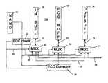
- FIG. 1there is shown an output buffer circuit 10 of the prior art.
- a NAND memory 12provides data output.
- the data bits and the accompanying ECC bitsare supplied to a first multiplexer 14 . From there the data is supplied either to a first buffer 16 or a second buffer 18 . From the first buffer 16 or the second buffer 18 , the data is supplied to a second MUX 20 as the output of the buffer circuit 10 .
- the buffer circuit 10is known as ping-pong circuit. In operation, the circuit 10 functions as follows. In a rust clock cycle T 1 , the data from the NAND memory 12 is passed through MUX 14 and is stored in buffer 16 . The data in the buffer 16 is checked and corrected by ECC checking and correction circuits (not shown) if need be.
- a second clock cycle T 2the data from the NAND memory 12 is passed through MUX 14 and stored in buffer 18 and the data in the buffer 18 is checked and corrected by ECC checking and correction circuits (not shown) if need be, while the data from the buffer 16 is passed through the MUX 20 as the output of the buffer circuit 10 .
- a third clock cycle T 3the data from the NAND memory 12 is passed through MUX 14 and stored in buffer 16 and the data in the buffer 16 is checked and corrected by ECC checking and correction circuits (not shown) if need be, while the data from the buffer 18 is passed through the MUX 20 as the output of the buffer circuit 10
- the buffer circuit 10 of the prior artmaintains the consistency of performance even as ECC degrades over time, so long as the error checking and correction can be performed in one clock cycle.
- this assumptionis not true as more NAND memory chips use MLC memory cells and as the number of associated error correction bits increase.
- An output buffer circuit for a non-volatile memorystores a plurality of data bits and a plurality of error correction check (“ECC”) bits associated with the plurality of data bits.
- the output buffer circuitcomprises an error check circuit for receiving the plurality of data bits and the plurality of ECC bits to determine if the plurality of data bits need to be corrected.
- the error check circuitsupplies the plurality of data bits as its output, and generates a correction signal.
- An error correction circuitreceives the plurality of data bits and the plurality of BCC bits and generates a plurality of corrected data bits in response to the correction signal.
- the output buffer circuitfurther has three or more storage circuits with each storage circuit having an input/output port.
- a busconnects to each of the storage circuits and to each other and supplies data bits between each storage circuit and between the nonvolatile memory and the storage circuits, and supplies data bits as the output of the output buffer circuit.
- a switch circuitis associated with each storage circuit for receiving the plurality of data bits; or the plurality of corrected data bits, and supplies same to the input/output port of the associated storage circuit and stores same as storage bits in the storage circuit, and supplies the storage bits as output of the storage circuit.
- FIG. 1is a block diagram of an output buffer circuit of the prior art.
- FIG. 2is a block diagram of a first embodiment of an output buffer circuit of the present invention.
- FIG. 3is a block diagram of a first embodiment of a memory system showing a plurality of NAND memory chips using a plurality of output buffer circuits of the present invention.
- FIG. 4is a block diagram of a second embodiment of a memory system showing a plurality of NAND memory chips using a plurality of output buffer circuits of the present invention.
- FIG. 2there is shown a block level diagram of a first embodiment of an output buffer circuit 100 of the present invention for use with a NAND memory 12 .
- the data output from the NAND memory 12including a plurality of data bits, and the associated plurality of ECC bits are supplied to an error checking circuit 22 , where the data bits and the ECC bits are checked by the ECC Check circuit 22 to determine if an error correction algorithm needs to be applied to the data bits.
- the ECC Check circuitgenerates as an output thereof a correction control signal, in the event the uncorrected data bits need to be corrected.
- the uncorrected data bits from the ECC Check circuit 22are supplied along a data bus 60 .
- the ECC correction circuit 24receives the uncorrected data bits and the associated ECC bits along the uncorrected bus 60 and performs a correction to the uncorrected data bits and generates a plurality of corrected data bits, in response to the correction control signal.
- the plurality of corrected data bitsare supplied along the corrected data bus 62 .
- Each storage bufferhas an associated input/output port: 31 , 33 , and 35 , respectively.
- the input/output ports 31 , 33 , 35are connected to a MUX 40 , 42 and 44 respectively.
- Each MUX 40 , 42 , and 44has three inputs: 1) a first input connected to the uncorrected data bus 60 for receiving the uncorrected data bits from the ECC check circuit 22 or from the output of the NAND memory 12 ; 2) a second input connected to the corrected data bus 62 , which receives the corrected data bits from the ECC correction circuit 24 ; and 3) a third input connected to an input/output bus 64 which is connected to all of the other MUXs and provides as an output of the output buffer circuit 100 .
- the correction control signal front the ECC check circuit 22controls the switching and the timing of thereof for each of the MUX 40 , 42 , and 44 .
- the data bits and the associated ECC bitsare read from the NAND memory 12 and supplied to the ECC check circuit 22 .
- the ECC check circuit 22performs an operation to determine whether the data bits need any correction.
- the data bitsare also sent and stored in the first buffer 30 , irrespective of the result of the operation by the ECC check circuit 22 .
- a second clock cycle T 2if the result of the ECC check circuit 22 shows that the data bits do not need any correction, then the uncorrected data from the first buffer 30 is outputted from the first buffer 30 and supplied along the bus 64 , and stored in the third buffer 34 .
- the data from the NAND memory 12is read and is stored in the first buffer 30 , as described above.
- the designation of the Mux 40 , 42 , 44 associated with the buffers 30 , 32 and 34may simply be switched without the data being outputted from one buffer and read into another buffer.
- the buffer 30may then be designated as the “out buffer 34 ” and the buffer 34 may be designated as a “in buffer” 30 .
- the uncorrected data bitsare stored in the first buffer 30 and sent to the ECC correction circuit 24 , as described above. If the ECC check circuit 22 determines correction is necessary, a correction control signal is generated which causes the ECC correction circuit 24 to commence the correction of the uncorrected data bits based upon the uncorrected data bits and the associated ECC bits. In addition, the ECC check 22 causes the “In buffer” 30 to be the “ECC Buffer” 32 , and the ECC buffer 32 to be the In buffer 30 .
- the uncorrected data bitsare corrected by the ECC correction circuit 24 , and stored in the second buffer 32 , or are corrected in the buffer 32 directly.
- the uncorrected data bits from that read cycleis then stored in the first buffer 30 .
- a third clock cycle T 3the corrected data bits stored in second storage buffer 32 are then read from the second storage buffer 32 and stored in the third storage buffer 34 .
- those uncorrected data bitsare corrected by the ECC correction circuit 24 , and stored in the second storage buffer 32 .
- uncorrected data bitsare read, from the NAND memory 12 , they are stored in the first storage buffer 30 .
- data from the output buffer circuit 100can be outputted at every clock cycle, thereafter.
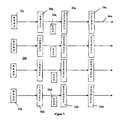
- FIG. 3there is shown a block level diagram of a first embodiment of a memory system 200 using a plurality of the output buffer circuits 100 of the present invention.
- the memory system 200comprises a plurality of NAND memories 12 ( a - d ) (only 4 are shown for illustration purpose).
- Each of the NAND memories 12has an associated output buffer circuit 100 shown and described in FIG. 2 .
- FIG. 3For simplicity only a portion of the output buffer circuit 100 is shown in FIG. 3 .
- Each of the output buffer circuit 100is shown with an ECC correction circuit 24 .
- the memory system. 200comprises a plurality of NAND memories 24 , each with an associated output buffer circuit 100 , with each output buffer circuit 100 having a dedicated ECC correction circuit 24 .
- FIG. 4there is shown a block level diagram of a second embodiment of a memory system 210 using a plurality of the output buffer circuits 100 of the present invention.
- the memory system 210comprises a plurality of NAND memories 12 ( a - d ) (only 4 are shown for illustration purpose).
- Each of the NAND memories 12has an associated output buffer circuit. 100 shown and described in FIG. 2 .
- the plurality of output buffer circuits 100all share a single ECC correction circuit 24 .
- the ECC correction circuit 24can perform rapid enough correction, then it can serve as the correction circuit for all four output buffers 100 ( a - d ).
- a single ECC correction circuit 24may serve a plurality of output buffer circuits 100 as shown.
- the memory system 210 shown in FIG. 4is similar to the memory system shown in FIG. 3 .
- an output buffer circuit for a NAND chipwhich can overcome the problem of ECC affecting performance as the NAND chip degrades over time.
Landscapes
- Engineering & Computer Science (AREA)
- Theoretical Computer Science (AREA)
- Physics & Mathematics (AREA)
- Probability & Statistics with Applications (AREA)
- Quality & Reliability (AREA)
- General Engineering & Computer Science (AREA)
- General Physics & Mathematics (AREA)
- Techniques For Improving Reliability Of Storages (AREA)
- Detection And Correction Of Errors (AREA)
- For Increasing The Reliability Of Semiconductor Memories (AREA)
Abstract
Description
Claims (14)
Priority Applications (5)
| Application Number | Priority Date | Filing Date | Title |
|---|---|---|---|
| US12/791,774US8726130B2 (en) | 2010-06-01 | 2010-06-01 | Dynamic buffer management in a NAND memory controller to minimize age related performance degradation due to error correction |
| EP11790176.9AEP2577666A4 (en) | 2010-06-01 | 2011-05-16 | Dynamic buffer management in a nand memory controller to minimize age related performance degradation due to error correction |
| JP2013513197AJP5563719B2 (en) | 2010-06-01 | 2011-05-16 | Dynamic buffer management in NAND memory controller to minimize aging-related performance degradation due to error correction |
| PCT/US2011/036669WO2011152985A1 (en) | 2010-06-01 | 2011-05-16 | Dynamic buffer management in a nand memory controller to minimize age related performance degradation due to error correction |
| CN201180027124.3ACN103038829B (en) | 2010-06-01 | 2011-05-16 | Dynamic Buffer Management in NAND Memory Controllers to Minimize Aging-Related Performance Degradation Due to Error Correction |
Applications Claiming Priority (1)
| Application Number | Priority Date | Filing Date | Title |
|---|---|---|---|
| US12/791,774US8726130B2 (en) | 2010-06-01 | 2010-06-01 | Dynamic buffer management in a NAND memory controller to minimize age related performance degradation due to error correction |
Publications (2)
| Publication Number | Publication Date |
|---|---|
| US20110296276A1 US20110296276A1 (en) | 2011-12-01 |
| US8726130B2true US8726130B2 (en) | 2014-05-13 |
Family
ID=45023174
Family Applications (1)
| Application Number | Title | Priority Date | Filing Date |
|---|---|---|---|
| US12/791,774Active2031-12-11US8726130B2 (en) | 2010-06-01 | 2010-06-01 | Dynamic buffer management in a NAND memory controller to minimize age related performance degradation due to error correction |
Country Status (5)
| Country | Link |
|---|---|
| US (1) | US8726130B2 (en) |
| EP (1) | EP2577666A4 (en) |
| JP (1) | JP5563719B2 (en) |
| CN (1) | CN103038829B (en) |
| WO (1) | WO2011152985A1 (en) |
Families Citing this family (2)
| Publication number | Priority date | Publication date | Assignee | Title |
|---|---|---|---|---|
| CN106355246B (en)* | 2015-10-08 | 2019-02-15 | 上海兆芯集成电路有限公司 | Three Configuration Neural Network Units |
| FR3066033B1 (en)* | 2017-05-05 | 2019-06-21 | Stmicroelectronics (Rousset) Sas | BUFFER STAGE DEVICE, PARTICULARLY ABLE TO BE CONNECTED TO A BUS OF THE SERIAL PERIPHERAL INTERFACE TYPE |
Citations (17)
| Publication number | Priority date | Publication date | Assignee | Title |
|---|---|---|---|---|
| US5745508A (en)* | 1995-11-13 | 1998-04-28 | Tricord Systems, Inc. | Error-detection code |
| JPH10143331A (en) | 1996-11-11 | 1998-05-29 | Xing:Kk | Storage device array system |
| US6003151A (en) | 1997-02-04 | 1999-12-14 | Mediatek Inc. | Error correction and detection system for mass storage controller |
| US6009548A (en)* | 1997-12-03 | 1999-12-28 | International Business Machines Corporation | Error correcting code retrofit method and apparatus for multiple memory configurations |
| US6044483A (en)* | 1998-01-29 | 2000-03-28 | International Business Machines Corporation | Error propagation operating mode for error correcting code retrofit apparatus |
| EP1065594A2 (en) | 1999-06-28 | 2001-01-03 | Kabushiki Kaisha Toshiba | Error detection and correction circuit in a flash memory |
| US6317371B2 (en) | 1996-02-29 | 2001-11-13 | Hitachi, Ltd. | Storage device with an error correction unit and an improved arrangement for accessing and transferring blocks of data stored in a non-volatile semiconductor memory |
| US6499082B1 (en) | 1999-04-16 | 2002-12-24 | Via Technologies, Inc. | Method of transferring data from large capacity data storage device |
| US6731537B2 (en)* | 2001-09-12 | 2004-05-04 | Renesas Technology Corp. | Non-volatile memory device and data storing method |
| US20050005230A1 (en) | 2003-06-30 | 2005-01-06 | Mitsuhiro Koga | Semiconductor integrated circuit device and error checking and correcting method thereof |
| US7073099B1 (en)* | 2002-05-30 | 2006-07-04 | Marvell International Ltd. | Method and apparatus for improving memory operation and yield |
| US20070121359A1 (en) | 2005-10-07 | 2007-05-31 | Kazushige Kanda | Semiconductor memory device with mos transistors each having floating gate and control gate |
| JP2008004111A (en) | 1996-02-29 | 2008-01-10 | Renesas Technology Corp | Semiconductor memory device |
| US20080008001A1 (en) | 2006-05-10 | 2008-01-10 | Nec Electronics Corporation | Semiconductor device and boot method for the same |
| US20090141560A1 (en) | 2007-11-29 | 2009-06-04 | Hynix Semiconductor Inc. | Flash memory device and programming method thereof |
| US20090282308A1 (en)* | 2008-05-09 | 2009-11-12 | Jan Gutsche | Memory Cell Arrangement and Method for Reading State Information From a Memory Cell Bypassing an Error Detection Circuit |
| US7940575B2 (en)* | 2008-03-28 | 2011-05-10 | Qimonda Ag | Memory device and method providing logic connections for data transfer |
Family Cites Families (1)
| Publication number | Priority date | Publication date | Assignee | Title |
|---|---|---|---|---|
| KR101425957B1 (en)* | 2007-08-21 | 2014-08-06 | 삼성전자주식회사 | Ecc control circuit and multi channel memory system icluding the same |
- 2010
- 2010-06-01USUS12/791,774patent/US8726130B2/enactiveActive
- 2011
- 2011-05-16JPJP2013513197Apatent/JP5563719B2/enactiveActive
- 2011-05-16EPEP11790176.9Apatent/EP2577666A4/ennot_activeCeased
- 2011-05-16CNCN201180027124.3Apatent/CN103038829B/enactiveActive
- 2011-05-16WOPCT/US2011/036669patent/WO2011152985A1/enactiveApplication Filing
Patent Citations (23)
| Publication number | Priority date | Publication date | Assignee | Title |
|---|---|---|---|---|
| US5745508A (en)* | 1995-11-13 | 1998-04-28 | Tricord Systems, Inc. | Error-detection code |
| US6317371B2 (en) | 1996-02-29 | 2001-11-13 | Hitachi, Ltd. | Storage device with an error correction unit and an improved arrangement for accessing and transferring blocks of data stored in a non-volatile semiconductor memory |
| JP2008004111A (en) | 1996-02-29 | 2008-01-10 | Renesas Technology Corp | Semiconductor memory device |
| JPH10143331A (en) | 1996-11-11 | 1998-05-29 | Xing:Kk | Storage device array system |
| US6003151A (en) | 1997-02-04 | 1999-12-14 | Mediatek Inc. | Error correction and detection system for mass storage controller |
| US6009548A (en)* | 1997-12-03 | 1999-12-28 | International Business Machines Corporation | Error correcting code retrofit method and apparatus for multiple memory configurations |
| US6018817A (en)* | 1997-12-03 | 2000-01-25 | International Business Machines Corporation | Error correcting code retrofit method and apparatus for multiple memory configurations |
| US6044483A (en)* | 1998-01-29 | 2000-03-28 | International Business Machines Corporation | Error propagation operating mode for error correcting code retrofit apparatus |
| US6499082B1 (en) | 1999-04-16 | 2002-12-24 | Via Technologies, Inc. | Method of transferring data from large capacity data storage device |
| EP1065594A2 (en) | 1999-06-28 | 2001-01-03 | Kabushiki Kaisha Toshiba | Error detection and correction circuit in a flash memory |
| US7116578B2 (en)* | 2001-09-12 | 2006-10-03 | Renesas Technology Corp. | Non-volatile memory device and data storing method |
| US6731537B2 (en)* | 2001-09-12 | 2004-05-04 | Renesas Technology Corp. | Non-volatile memory device and data storing method |
| US20070168781A1 (en)* | 2002-05-30 | 2007-07-19 | Sehat Sutardja | Fully-buffered dual in-line memory module with fault correction |
| US7073099B1 (en)* | 2002-05-30 | 2006-07-04 | Marvell International Ltd. | Method and apparatus for improving memory operation and yield |
| US7962809B1 (en)* | 2002-05-30 | 2011-06-14 | Marvell International Ltd. | Method and apparatus for improving memory operation and yield |
| US20050005230A1 (en) | 2003-06-30 | 2005-01-06 | Mitsuhiro Koga | Semiconductor integrated circuit device and error checking and correcting method thereof |
| US20070121359A1 (en) | 2005-10-07 | 2007-05-31 | Kazushige Kanda | Semiconductor memory device with mos transistors each having floating gate and control gate |
| US7428161B2 (en)* | 2005-10-07 | 2008-09-23 | Kabushiki Kaisha Toshiba | Semiconductor memory device with MOS transistors each having floating gate and control gate |
| US20080008001A1 (en) | 2006-05-10 | 2008-01-10 | Nec Electronics Corporation | Semiconductor device and boot method for the same |
| US8037358B2 (en)* | 2006-05-10 | 2011-10-11 | Renesas Electronics Corporation | Semiconductor device and boot method for the same |
| US20090141560A1 (en) | 2007-11-29 | 2009-06-04 | Hynix Semiconductor Inc. | Flash memory device and programming method thereof |
| US7940575B2 (en)* | 2008-03-28 | 2011-05-10 | Qimonda Ag | Memory device and method providing logic connections for data transfer |
| US20090282308A1 (en)* | 2008-05-09 | 2009-11-12 | Jan Gutsche | Memory Cell Arrangement and Method for Reading State Information From a Memory Cell Bypassing an Error Detection Circuit |
Non-Patent Citations (3)
| Title |
|---|
| Japanese Office Action dated Jan. 6, 2014 pertaining to the related Korean Patent Application No. 2013-513197. (English and Japanese translations). |
| PCT Search Report and Written Opinion mailed on Aug. 19, 2011 corresponding to the related PCT Patent Application No. US11/36669. |
| The Extended European Search Report dated Oct. 7, 2013 corresponding to the related European Patent Application No. 11790176.9. |
Also Published As
| Publication number | Publication date |
|---|---|
| US20110296276A1 (en) | 2011-12-01 |
| JP2013527544A (en) | 2013-06-27 |
| CN103038829B (en) | 2016-01-06 |
| EP2577666A4 (en) | 2013-11-06 |
| WO2011152985A1 (en) | 2011-12-08 |
| CN103038829A (en) | 2013-04-10 |
| EP2577666A1 (en) | 2013-04-10 |
| JP5563719B2 (en) | 2014-07-30 |
Similar Documents
| Publication | Publication Date | Title |
|---|---|---|
| US8656252B2 (en) | Memory controller and non-volatile storage device | |
| US9411680B2 (en) | Composite semiconductor memory device with error correction | |
| US9128822B2 (en) | On-chip bad block management for NAND flash memory | |
| US20080222491A1 (en) | Flash memory system for improving read performance and read method thereof | |
| US8910018B2 (en) | Memory with dynamic error detection and correction | |
| US10782920B2 (en) | Data access method, memory storage apparatus and memory control circuit unit | |
| KR20090019593A (en) | IC control circuit and multichannel memory system including the same | |
| US7257762B2 (en) | Memory interface with write buffer and encoder | |
| US7656322B2 (en) | Semiconductor memory device having error correction function | |
| US20150081962A1 (en) | Cache memory device and data processing method of the device | |
| US11101822B1 (en) | Data writing method, memory control circuit unit and memory storage apparatus | |
| US11023165B2 (en) | Memory control circuit unit, storage device and method including selectively performing or ignoring commands in a command queue after a power glitch | |
| US8898420B2 (en) | Non-volatile storage device and a memory controller controlling parity tables of recording regions of the non-volatile storage device | |
| US11301311B2 (en) | Memory control method, memory storage device, and memory control circuit unit | |
| US7310262B2 (en) | Ferroelectric memory capable of continuously fast transferring data words in a pipeline | |
| US20180335942A1 (en) | Data reading method, memory control circuit unit and memory storage device | |
| US7180824B2 (en) | Semiconductor memory device with a page mode | |
| US8726130B2 (en) | Dynamic buffer management in a NAND memory controller to minimize age related performance degradation due to error correction | |
| JP4254932B2 (en) | Memory controller and flash memory system | |
| US11409596B1 (en) | Encoding control method, memory storage device and memory control circuit unit | |
| US8897048B2 (en) | Semiconductor memory device and programming method thereof | |
| US20240289062A1 (en) | Raid controller, operating method of raid controller and storage device | |
| US12051480B2 (en) | Semiconductor storage device | |
| US11775205B2 (en) | Semiconductor storage device and reading method | |
| JP2006113790A (en) | Storage device, data processing system and memory control method |
Legal Events
| Date | Code | Title | Description |
|---|---|---|---|
| AS | Assignment | Owner name:SILICON STORAGE TECHNOLOGY, INC., CALIFORNIA Free format text:ASSIGNMENT OF ASSIGNORS INTEREST;ASSIGNOR:ARYA, SIAMAK;REEL/FRAME:024533/0587 Effective date:20100517 | |
| AS | Assignment | Owner name:GREENLIANT SYSTEMS, INC., CALIFORNIA Free format text:NUNC PRO TUNC ASSIGNMENT;ASSIGNOR:SILICON STORAGE TECHNOLOGY, INC.;REEL/FRAME:024776/0624 Effective date:20100521 Owner name:GREENLIANT LLC, CALIFORNIA Free format text:ASSIGNMENT OF ASSIGNORS INTEREST;ASSIGNOR:GREENLIANT SYSTEMS, INC.;REEL/FRAME:024776/0637 Effective date:20100709 | |
| STCF | Information on status: patent grant | Free format text:PATENTED CASE | |
| MAFP | Maintenance fee payment | Free format text:PAYMENT OF MAINTENANCE FEE, 4TH YEAR, LARGE ENTITY (ORIGINAL EVENT CODE: M1551) Year of fee payment:4 | |
| MAFP | Maintenance fee payment | Free format text:PAYMENT OF MAINTENANCE FEE, 8TH YEAR, LARGE ENTITY (ORIGINAL EVENT CODE: M1552); ENTITY STATUS OF PATENT OWNER: LARGE ENTITY Year of fee payment:8 |