US8723332B2 - Electrically interconnected stacked die assemblies - Google Patents
Electrically interconnected stacked die assembliesDownload PDFInfo
- Publication number
- US8723332B2 US8723332B2US12/124,077US12407708AUS8723332B2US 8723332 B2US8723332 B2US 8723332B2US 12407708 AUS12407708 AUS 12407708AUS 8723332 B2US8723332 B2US 8723332B2
- Authority
- US
- United States
- Prior art keywords
- die
- interconnect
- stack
- stacked
- assembly
- Prior art date
- Legal status (The legal status is an assumption and is not a legal conclusion. Google has not performed a legal analysis and makes no representation as to the accuracy of the status listed.)
- Active, expires
Links
Images


Classifications
- H—ELECTRICITY
- H01—ELECTRIC ELEMENTS
- H01L—SEMICONDUCTOR DEVICES NOT COVERED BY CLASS H10
- H01L25/00—Assemblies consisting of a plurality of semiconductor or other solid state devices
- H01L25/50—Multistep manufacturing processes of assemblies consisting of devices, the devices being individual devices of subclass H10D or integrated devices of class H10
- H—ELECTRICITY
- H01—ELECTRIC ELEMENTS
- H01L—SEMICONDUCTOR DEVICES NOT COVERED BY CLASS H10
- H01L24/00—Arrangements for connecting or disconnecting semiconductor or solid-state bodies; Methods or apparatus related thereto
- H01L24/01—Means for bonding being attached to, or being formed on, the surface to be connected, e.g. chip-to-package, die-attach, "first-level" interconnects; Manufacturing methods related thereto
- H01L24/18—High density interconnect [HDI] connectors; Manufacturing methods related thereto
- H01L24/23—Structure, shape, material or disposition of the high density interconnect connectors after the connecting process
- H01L24/24—Structure, shape, material or disposition of the high density interconnect connectors after the connecting process of an individual high density interconnect connector
- H—ELECTRICITY
- H01—ELECTRIC ELEMENTS
- H01L—SEMICONDUCTOR DEVICES NOT COVERED BY CLASS H10
- H01L24/00—Arrangements for connecting or disconnecting semiconductor or solid-state bodies; Methods or apparatus related thereto
- H01L24/01—Means for bonding being attached to, or being formed on, the surface to be connected, e.g. chip-to-package, die-attach, "first-level" interconnects; Manufacturing methods related thereto
- H01L24/18—High density interconnect [HDI] connectors; Manufacturing methods related thereto
- H01L24/23—Structure, shape, material or disposition of the high density interconnect connectors after the connecting process
- H01L24/25—Structure, shape, material or disposition of the high density interconnect connectors after the connecting process of a plurality of high density interconnect connectors
- H—ELECTRICITY
- H01—ELECTRIC ELEMENTS
- H01L—SEMICONDUCTOR DEVICES NOT COVERED BY CLASS H10
- H01L24/00—Arrangements for connecting or disconnecting semiconductor or solid-state bodies; Methods or apparatus related thereto
- H01L24/80—Methods for connecting semiconductor or other solid state bodies using means for bonding being attached to, or being formed on, the surface to be connected
- H01L24/82—Methods for connecting semiconductor or other solid state bodies using means for bonding being attached to, or being formed on, the surface to be connected by forming build-up interconnects at chip-level, e.g. for high density interconnects [HDI]
- H—ELECTRICITY
- H01—ELECTRIC ELEMENTS
- H01L—SEMICONDUCTOR DEVICES NOT COVERED BY CLASS H10
- H01L25/00—Assemblies consisting of a plurality of semiconductor or other solid state devices
- H01L25/03—Assemblies consisting of a plurality of semiconductor or other solid state devices all the devices being of a type provided for in a single subclass of subclasses H10B, H10D, H10F, H10H, H10K or H10N, e.g. assemblies of rectifier diodes
- H01L25/04—Assemblies consisting of a plurality of semiconductor or other solid state devices all the devices being of a type provided for in a single subclass of subclasses H10B, H10D, H10F, H10H, H10K or H10N, e.g. assemblies of rectifier diodes the devices not having separate containers
- H01L25/065—Assemblies consisting of a plurality of semiconductor or other solid state devices all the devices being of a type provided for in a single subclass of subclasses H10B, H10D, H10F, H10H, H10K or H10N, e.g. assemblies of rectifier diodes the devices not having separate containers the devices being of a type provided for in group H10D89/00
- H01L25/0657—Stacked arrangements of devices
- H—ELECTRICITY
- H01—ELECTRIC ELEMENTS
- H01L—SEMICONDUCTOR DEVICES NOT COVERED BY CLASS H10
- H01L2224/00—Indexing scheme for arrangements for connecting or disconnecting semiconductor or solid-state bodies and methods related thereto as covered by H01L24/00
- H01L2224/01—Means for bonding being attached to, or being formed on, the surface to be connected, e.g. chip-to-package, die-attach, "first-level" interconnects; Manufacturing methods related thereto
- H01L2224/18—High density interconnect [HDI] connectors; Manufacturing methods related thereto
- H01L2224/23—Structure, shape, material or disposition of the high density interconnect connectors after the connecting process
- H01L2224/24—Structure, shape, material or disposition of the high density interconnect connectors after the connecting process of an individual high density interconnect connector
- H01L2224/2401—Structure
- H01L2224/24011—Deposited, e.g. MCM-D type
- H—ELECTRICITY
- H01—ELECTRIC ELEMENTS
- H01L—SEMICONDUCTOR DEVICES NOT COVERED BY CLASS H10
- H01L2224/00—Indexing scheme for arrangements for connecting or disconnecting semiconductor or solid-state bodies and methods related thereto as covered by H01L24/00
- H01L2224/01—Means for bonding being attached to, or being formed on, the surface to be connected, e.g. chip-to-package, die-attach, "first-level" interconnects; Manufacturing methods related thereto
- H01L2224/18—High density interconnect [HDI] connectors; Manufacturing methods related thereto
- H01L2224/23—Structure, shape, material or disposition of the high density interconnect connectors after the connecting process
- H01L2224/24—Structure, shape, material or disposition of the high density interconnect connectors after the connecting process of an individual high density interconnect connector
- H01L2224/241—Disposition
- H01L2224/24135—Connecting between different semiconductor or solid-state bodies, i.e. chip-to-chip
- H01L2224/24145—Connecting between different semiconductor or solid-state bodies, i.e. chip-to-chip the bodies being stacked
- H—ELECTRICITY
- H01—ELECTRIC ELEMENTS
- H01L—SEMICONDUCTOR DEVICES NOT COVERED BY CLASS H10
- H01L2224/00—Indexing scheme for arrangements for connecting or disconnecting semiconductor or solid-state bodies and methods related thereto as covered by H01L24/00
- H01L2224/01—Means for bonding being attached to, or being formed on, the surface to be connected, e.g. chip-to-package, die-attach, "first-level" interconnects; Manufacturing methods related thereto
- H01L2224/18—High density interconnect [HDI] connectors; Manufacturing methods related thereto
- H01L2224/23—Structure, shape, material or disposition of the high density interconnect connectors after the connecting process
- H01L2224/24—Structure, shape, material or disposition of the high density interconnect connectors after the connecting process of an individual high density interconnect connector
- H01L2224/241—Disposition
- H01L2224/24151—Connecting between a semiconductor or solid-state body and an item not being a semiconductor or solid-state body, e.g. chip-to-substrate, chip-to-passive
- H01L2224/24221—Connecting between a semiconductor or solid-state body and an item not being a semiconductor or solid-state body, e.g. chip-to-substrate, chip-to-passive the body and the item being stacked
- H01L2224/24225—Connecting between a semiconductor or solid-state body and an item not being a semiconductor or solid-state body, e.g. chip-to-substrate, chip-to-passive the body and the item being stacked the item being non-metallic, e.g. insulating substrate with or without metallisation
- H01L2224/24226—Connecting between a semiconductor or solid-state body and an item not being a semiconductor or solid-state body, e.g. chip-to-substrate, chip-to-passive the body and the item being stacked the item being non-metallic, e.g. insulating substrate with or without metallisation the HDI interconnect connecting to the same level of the item at which the semiconductor or solid-state body is mounted, e.g. the item being planar
- H—ELECTRICITY
- H01—ELECTRIC ELEMENTS
- H01L—SEMICONDUCTOR DEVICES NOT COVERED BY CLASS H10
- H01L2224/00—Indexing scheme for arrangements for connecting or disconnecting semiconductor or solid-state bodies and methods related thereto as covered by H01L24/00
- H01L2224/01—Means for bonding being attached to, or being formed on, the surface to be connected, e.g. chip-to-package, die-attach, "first-level" interconnects; Manufacturing methods related thereto
- H01L2224/26—Layer connectors, e.g. plate connectors, solder or adhesive layers; Manufacturing methods related thereto
- H01L2224/31—Structure, shape, material or disposition of the layer connectors after the connecting process
- H01L2224/32—Structure, shape, material or disposition of the layer connectors after the connecting process of an individual layer connector
- H01L2224/321—Disposition
- H01L2224/32135—Disposition the layer connector connecting between different semiconductor or solid-state bodies, i.e. chip-to-chip
- H01L2224/32145—Disposition the layer connector connecting between different semiconductor or solid-state bodies, i.e. chip-to-chip the bodies being stacked
- H—ELECTRICITY
- H01—ELECTRIC ELEMENTS
- H01L—SEMICONDUCTOR DEVICES NOT COVERED BY CLASS H10
- H01L2224/00—Indexing scheme for arrangements for connecting or disconnecting semiconductor or solid-state bodies and methods related thereto as covered by H01L24/00
- H01L2224/01—Means for bonding being attached to, or being formed on, the surface to be connected, e.g. chip-to-package, die-attach, "first-level" interconnects; Manufacturing methods related thereto
- H01L2224/42—Wire connectors; Manufacturing methods related thereto
- H01L2224/47—Structure, shape, material or disposition of the wire connectors after the connecting process
- H01L2224/48—Structure, shape, material or disposition of the wire connectors after the connecting process of an individual wire connector
- H01L2224/4805—Shape
- H01L2224/4809—Loop shape
- H01L2224/48091—Arched
- H—ELECTRICITY
- H01—ELECTRIC ELEMENTS
- H01L—SEMICONDUCTOR DEVICES NOT COVERED BY CLASS H10
- H01L2224/00—Indexing scheme for arrangements for connecting or disconnecting semiconductor or solid-state bodies and methods related thereto as covered by H01L24/00
- H01L2224/01—Means for bonding being attached to, or being formed on, the surface to be connected, e.g. chip-to-package, die-attach, "first-level" interconnects; Manufacturing methods related thereto
- H01L2224/42—Wire connectors; Manufacturing methods related thereto
- H01L2224/47—Structure, shape, material or disposition of the wire connectors after the connecting process
- H01L2224/48—Structure, shape, material or disposition of the wire connectors after the connecting process of an individual wire connector
- H01L2224/4805—Shape
- H01L2224/4809—Loop shape
- H01L2224/48095—Kinked
- H—ELECTRICITY
- H01—ELECTRIC ELEMENTS
- H01L—SEMICONDUCTOR DEVICES NOT COVERED BY CLASS H10
- H01L2224/00—Indexing scheme for arrangements for connecting or disconnecting semiconductor or solid-state bodies and methods related thereto as covered by H01L24/00
- H01L2224/01—Means for bonding being attached to, or being formed on, the surface to be connected, e.g. chip-to-package, die-attach, "first-level" interconnects; Manufacturing methods related thereto
- H01L2224/42—Wire connectors; Manufacturing methods related thereto
- H01L2224/47—Structure, shape, material or disposition of the wire connectors after the connecting process
- H01L2224/48—Structure, shape, material or disposition of the wire connectors after the connecting process of an individual wire connector
- H01L2224/481—Disposition
- H01L2224/48135—Connecting between different semiconductor or solid-state bodies, i.e. chip-to-chip
- H01L2224/48145—Connecting between different semiconductor or solid-state bodies, i.e. chip-to-chip the bodies being stacked
- H—ELECTRICITY
- H01—ELECTRIC ELEMENTS
- H01L—SEMICONDUCTOR DEVICES NOT COVERED BY CLASS H10
- H01L2224/00—Indexing scheme for arrangements for connecting or disconnecting semiconductor or solid-state bodies and methods related thereto as covered by H01L24/00
- H01L2224/01—Means for bonding being attached to, or being formed on, the surface to be connected, e.g. chip-to-package, die-attach, "first-level" interconnects; Manufacturing methods related thereto
- H01L2224/42—Wire connectors; Manufacturing methods related thereto
- H01L2224/47—Structure, shape, material or disposition of the wire connectors after the connecting process
- H01L2224/48—Structure, shape, material or disposition of the wire connectors after the connecting process of an individual wire connector
- H01L2224/484—Connecting portions
- H01L2224/48463—Connecting portions the connecting portion on the bonding area of the semiconductor or solid-state body being a ball bond
- H01L2224/48465—Connecting portions the connecting portion on the bonding area of the semiconductor or solid-state body being a ball bond the other connecting portion not on the bonding area being a wedge bond, i.e. ball-to-wedge, regular stitch
- H—ELECTRICITY
- H01—ELECTRIC ELEMENTS
- H01L—SEMICONDUCTOR DEVICES NOT COVERED BY CLASS H10
- H01L2224/00—Indexing scheme for arrangements for connecting or disconnecting semiconductor or solid-state bodies and methods related thereto as covered by H01L24/00
- H01L2224/74—Apparatus for manufacturing arrangements for connecting or disconnecting semiconductor or solid-state bodies and for methods related thereto
- H01L2224/76—Apparatus for connecting with build-up interconnects
- H01L2224/7615—Means for depositing
- H01L2224/76151—Means for direct writing
- H01L2224/76155—Jetting means, e.g. ink jet
- H—ELECTRICITY
- H01—ELECTRIC ELEMENTS
- H01L—SEMICONDUCTOR DEVICES NOT COVERED BY CLASS H10
- H01L2224/00—Indexing scheme for arrangements for connecting or disconnecting semiconductor or solid-state bodies and methods related thereto as covered by H01L24/00
- H01L2224/80—Methods for connecting semiconductor or other solid state bodies using means for bonding being attached to, or being formed on, the surface to be connected
- H01L2224/82—Methods for connecting semiconductor or other solid state bodies using means for bonding being attached to, or being formed on, the surface to be connected by forming build-up interconnects at chip-level, e.g. for high density interconnects [HDI]
- H01L2224/821—Forming a build-up interconnect
- H01L2224/82101—Forming a build-up interconnect by additive methods, e.g. direct writing
- H01L2224/82102—Forming a build-up interconnect by additive methods, e.g. direct writing using jetting, e.g. ink jet
- H—ELECTRICITY
- H01—ELECTRIC ELEMENTS
- H01L—SEMICONDUCTOR DEVICES NOT COVERED BY CLASS H10
- H01L2225/00—Details relating to assemblies covered by the group H01L25/00 but not provided for in its subgroups
- H01L2225/03—All the devices being of a type provided for in the same main group of the same subclass of class H10, e.g. assemblies of rectifier diodes
- H01L2225/04—All the devices being of a type provided for in the same main group of the same subclass of class H10, e.g. assemblies of rectifier diodes the devices not having separate containers
- H01L2225/065—All the devices being of a type provided for in the same main group of the same subclass of class H10
- H01L2225/06503—Stacked arrangements of devices
- H01L2225/06524—Electrical connections formed on device or on substrate, e.g. a deposited or grown layer
- H—ELECTRICITY
- H01—ELECTRIC ELEMENTS
- H01L—SEMICONDUCTOR DEVICES NOT COVERED BY CLASS H10
- H01L2225/00—Details relating to assemblies covered by the group H01L25/00 but not provided for in its subgroups
- H01L2225/03—All the devices being of a type provided for in the same main group of the same subclass of class H10, e.g. assemblies of rectifier diodes
- H01L2225/04—All the devices being of a type provided for in the same main group of the same subclass of class H10, e.g. assemblies of rectifier diodes the devices not having separate containers
- H01L2225/065—All the devices being of a type provided for in the same main group of the same subclass of class H10
- H01L2225/06503—Stacked arrangements of devices
- H01L2225/06551—Conductive connections on the side of the device
- H—ELECTRICITY
- H01—ELECTRIC ELEMENTS
- H01L—SEMICONDUCTOR DEVICES NOT COVERED BY CLASS H10
- H01L2225/00—Details relating to assemblies covered by the group H01L25/00 but not provided for in its subgroups
- H01L2225/03—All the devices being of a type provided for in the same main group of the same subclass of class H10, e.g. assemblies of rectifier diodes
- H01L2225/04—All the devices being of a type provided for in the same main group of the same subclass of class H10, e.g. assemblies of rectifier diodes the devices not having separate containers
- H01L2225/065—All the devices being of a type provided for in the same main group of the same subclass of class H10
- H01L2225/06503—Stacked arrangements of devices
- H01L2225/06555—Geometry of the stack, e.g. form of the devices, geometry to facilitate stacking
- H01L2225/06562—Geometry of the stack, e.g. form of the devices, geometry to facilitate stacking at least one device in the stack being rotated or offset
- H—ELECTRICITY
- H01—ELECTRIC ELEMENTS
- H01L—SEMICONDUCTOR DEVICES NOT COVERED BY CLASS H10
- H01L2924/00—Indexing scheme for arrangements or methods for connecting or disconnecting semiconductor or solid-state bodies as covered by H01L24/00
- H01L2924/01—Chemical elements
- H01L2924/01005—Boron [B]
- H—ELECTRICITY
- H01—ELECTRIC ELEMENTS
- H01L—SEMICONDUCTOR DEVICES NOT COVERED BY CLASS H10
- H01L2924/00—Indexing scheme for arrangements or methods for connecting or disconnecting semiconductor or solid-state bodies as covered by H01L24/00
- H01L2924/01—Chemical elements
- H01L2924/01006—Carbon [C]
- H—ELECTRICITY
- H01—ELECTRIC ELEMENTS
- H01L—SEMICONDUCTOR DEVICES NOT COVERED BY CLASS H10
- H01L2924/00—Indexing scheme for arrangements or methods for connecting or disconnecting semiconductor or solid-state bodies as covered by H01L24/00
- H01L2924/01—Chemical elements
- H01L2924/01013—Aluminum [Al]
- H—ELECTRICITY
- H01—ELECTRIC ELEMENTS
- H01L—SEMICONDUCTOR DEVICES NOT COVERED BY CLASS H10
- H01L2924/00—Indexing scheme for arrangements or methods for connecting or disconnecting semiconductor or solid-state bodies as covered by H01L24/00
- H01L2924/01—Chemical elements
- H01L2924/01015—Phosphorus [P]
- H—ELECTRICITY
- H01—ELECTRIC ELEMENTS
- H01L—SEMICONDUCTOR DEVICES NOT COVERED BY CLASS H10
- H01L2924/00—Indexing scheme for arrangements or methods for connecting or disconnecting semiconductor or solid-state bodies as covered by H01L24/00
- H01L2924/01—Chemical elements
- H01L2924/01033—Arsenic [As]
- H—ELECTRICITY
- H01—ELECTRIC ELEMENTS
- H01L—SEMICONDUCTOR DEVICES NOT COVERED BY CLASS H10
- H01L2924/00—Indexing scheme for arrangements or methods for connecting or disconnecting semiconductor or solid-state bodies as covered by H01L24/00
- H01L2924/01—Chemical elements
- H01L2924/01038—Strontium [Sr]
- H—ELECTRICITY
- H01—ELECTRIC ELEMENTS
- H01L—SEMICONDUCTOR DEVICES NOT COVERED BY CLASS H10
- H01L2924/00—Indexing scheme for arrangements or methods for connecting or disconnecting semiconductor or solid-state bodies as covered by H01L24/00
- H01L2924/01—Chemical elements
- H01L2924/01047—Silver [Ag]
- H—ELECTRICITY
- H01—ELECTRIC ELEMENTS
- H01L—SEMICONDUCTOR DEVICES NOT COVERED BY CLASS H10
- H01L2924/00—Indexing scheme for arrangements or methods for connecting or disconnecting semiconductor or solid-state bodies as covered by H01L24/00
- H01L2924/01—Chemical elements
- H01L2924/01074—Tungsten [W]
- H—ELECTRICITY
- H01—ELECTRIC ELEMENTS
- H01L—SEMICONDUCTOR DEVICES NOT COVERED BY CLASS H10
- H01L2924/00—Indexing scheme for arrangements or methods for connecting or disconnecting semiconductor or solid-state bodies as covered by H01L24/00
- H01L2924/01—Chemical elements
- H01L2924/01078—Platinum [Pt]
- H—ELECTRICITY
- H01—ELECTRIC ELEMENTS
- H01L—SEMICONDUCTOR DEVICES NOT COVERED BY CLASS H10
- H01L2924/00—Indexing scheme for arrangements or methods for connecting or disconnecting semiconductor or solid-state bodies as covered by H01L24/00
- H01L2924/01—Chemical elements
- H01L2924/01079—Gold [Au]
- H—ELECTRICITY
- H01—ELECTRIC ELEMENTS
- H01L—SEMICONDUCTOR DEVICES NOT COVERED BY CLASS H10
- H01L2924/00—Indexing scheme for arrangements or methods for connecting or disconnecting semiconductor or solid-state bodies as covered by H01L24/00
- H01L2924/01—Chemical elements
- H01L2924/01082—Lead [Pb]
- H—ELECTRICITY
- H01—ELECTRIC ELEMENTS
- H01L—SEMICONDUCTOR DEVICES NOT COVERED BY CLASS H10
- H01L2924/00—Indexing scheme for arrangements or methods for connecting or disconnecting semiconductor or solid-state bodies as covered by H01L24/00
- H01L2924/013—Alloys
- H01L2924/014—Solder alloys
- H—ELECTRICITY
- H01—ELECTRIC ELEMENTS
- H01L—SEMICONDUCTOR DEVICES NOT COVERED BY CLASS H10
- H01L2924/00—Indexing scheme for arrangements or methods for connecting or disconnecting semiconductor or solid-state bodies as covered by H01L24/00
- H01L2924/10—Details of semiconductor or other solid state devices to be connected
- H01L2924/11—Device type
- H01L2924/14—Integrated circuits
Definitions
- This inventionrelates to electrical interconnection of integrated circuit chips and, particularly, to interconnection of stacked die.
- a typical semiconductor diehas a front (“active”) side, in which the integrated circuitry is formed, a back side, and sidewalls. The sidewalls meet the front side at front edges and the back side at back edges.
- Semiconductor dietypically are provided with interconnect pads (die pads) located at the front side for electrical interconnection of the circuitry on the die with other circuitry in the device in which the die is deployed.
- Some die as providedhave die pads on the front side along one or more of the die margins, and these may be referred to as peripheral pad die.
- Other die as providedhave die pads arranged in one or two rows at the front side near the center of the die, and these may be referred to as central pad die.
- the diemay be “rerouted” to provide a suitable arrangement of interconnect pads at or near one or more of the margins of the die.
- Semiconductor diemay be electrically connected with other circuitry, for example in a printed circuit board, a package substrate or leadframe, or another die, by any of several means. Connection may be made, for example, by wire bonds, or by flip chip interconnects, or by tab interconnects.
- a number of approacheshave been proposed for increasing the density of active semiconductor circuitry in integrated circuit chip packages, while minimizing package size (package footprint, package thickness).
- package sizepackage footprint, package thickness.
- two or more semiconductor die, of the same or different functionalityare stacked one over another and mounted on a package substrate.
- Wire bond interconnectrequires both vertical clearance over the die surface at the front side margin, to accommodate the wire loop height, and horizontal clearance outside the die footprint, to accommodate the wire span. If the vertical clearance is insufficient, overlying features may interfere with or introduce electrical shorting to the wire loops. And, in practice, the lower interconnect pad or bond site must be located some distance away from the sidewall of the overlying die, so that the wire bonding tool does not impact the die edge during the bonding process, and so that the wire bond does not contact the front edge of the die.
- stacked semiconductor diepresents a number of challenges.
- two or more die in a stackmay be mounted on a substrate with their front sides facing away from the substrate, and connected by wire bonds die-to-substrate or die-to-die.
- Die-to-die wire bond interconnectmay be made where an upper die is dimensioned or located so that the upper die does not overlie the margin of the lower die to which it is connected, and so that sufficient horizontal clearance is provided for the wire span.
- This conditionmay pertain, for example, where the footprint of the upper die is sufficiently narrower than the lower die; or, for example, where the upper die is arranged so that the footprint of the upper die is offset in relation to the margin of the lower die.
- the die in the stackmay be indirectly interconnected by connecting them to a common substrate on which the stack is mounted.
- a spacermay be interposed to provide sufficient vertical clearance between the lower and the upper die to accommodate the wire loops over the lower die. The spacer adds to the thickness of the stack and, consequently, of the package.
- the wire bond die-to-substrate connection of the lower diemust be completed before the spacer and the upper die are stacked over it; that is, the die must be stacked in situ on the substrate and the die must be stacked and connected serially.
- the inventionfeatures die stack assembly configurations and interconnection means.
- two or more dieare stacked one over another; adjacent die in the stack are provided with interconnect pads arranged at the front side along a die margin, and the edge at the margin of a first die is offset in relation to the margin of the second die; and interconnect pads on the die are electrically connected by traces of an electrically conductive polymer.
- the offsetreveals at least a fraction of the area of the interconnect pads on the lower die, so that the pads on the lower die are available for electrical connection with pads on a die situated above.
- the dieare provided with an electrical insulation over at least the portions of the die surfaces over which the conductive traces are situated. In some embodiments the die are provided with an electrical insulation over at least those one or more sidewalls adjacent the die margin or die margins on which the interconnect pads are arranged; in some such embodiments the die are additionally provided with an electrical insulation over the front surface adjacent the die margin or die margins on which the interconnect pads are arranged, and in some such embodiments the die are additionally provided with an electrical insulation over back surface; in some embodiments the die are provided with an electrical insulation over the front surface, the back surface, and the sidewall surfaces of the die.
- the electrical insulationincludes an electrically insulative conformal coating.
- the conformal coatingprotects the die during assembly, and serves to electrically insulate the die from electrically conductive parts that it may contact.
- the material of the conformal coatingincludes a nonorganic polymer, such as for example a sol-gel glass deposit.
- the material of the conformal coatingincludes an organic polymer, such as for example a polyimid, a benzocyclobutene (BCB), an epoxy, or a cyanoacrylate; or a halogenated polymer such as for example a polymer of p-xylene or a derivative thereof, such as a polyxylylene polymer, e.g., a parylene C or a parylene N, or a parylene A, or a parylene SR.
- the conformal coatingis formed by deposition, for example by vapor deposition, or liquid phase deposition, or by solid phase deposition.
- Openings in the electrical insulationexpose at least selected die pads or interconnect terminals.
- the openingsmay in some embodiments be made following formation of the insulation.
- the electrical insulationincludes a conformal coating, such as a parylene
- openingsmay be made by removing spots of the conformal coating over the selected die pads.
- a lasermay be used to effect targeted removal of the conformal coating.
- the openingscan optionally be made following stacking the die.
- the electrical insulationmay be applied to the die prior to stacking; or, the electrical insulation may be applied to the stack of die after stacking; or, the electrical insulation may be applied to the die prior to stacking as well as to the stack.
- the interconnect materialis an electrically conductive polymer, such as a curable conductive epoxy, for example.
- the interconnect materialis applied using an application tool such as, for example, a syringe or a nozzle or a needle. The material exits the tool in a deposition direction generally toward the die pads or interconnect terminals, and the tool is moved over the presented stack face in a work direction to form a trace.
- the materialmay be extruded from the tool in a continuous flow; or, the extrusion of the material may be pulsed; or, the flow may be interrupted by valving; or, the material may exit the tool dropwise.
- the materialexits the tool as a jet of droplets, and is deposited as dots which coalesce upon contact, or following contact, with a stack face surface.
- the deposition directionis generally perpendicular to the die edge surface, and in other embodiments the deposition direction is at an angle off perpendicular to the die edge surface.
- the toolmay be moved in a generally linear work direction, or in a zig-zag work direction, depending upon the location on the various die of the corresponding terminals to be connected.
- the tracemay be branched or forked (for example, a “Y” trace), or unbranched.
- the tracesare formed one at a time. In some embodiments more than one interconnect trace is formed in a single interconnect operation, and in some such embodiments all the interconnect traces on a given stacked assembly are formed in a single operation (or in a number of operations fewer than the number of traces).
- the application toolmay in such instances include a number of needles or nozzles ganged together in a row generally parallel to the die edges.
- interconnect traces between pairs of vertically adjacent dieare made simultaneously, rather than serially, as suggested in FIGS. 4B , 5 , and in some such embodiments all the interconnections along a “vertical” direction (for example, direction W in FIGS. 4B , 5 , or a direction opposite direction W as shown) are made at once.
- the application toolmay include a number of needles or nozzles ganged together in a column generally parallel to the interconnect tract direction W.
- the interconnectsare applied by printing, for example using a print head (which may have a suitable array of nozzles), or for example by screen printing or stencil printing, or using a mask.
- Printingmay in some embodiments be carried out using a print head having an array of print nozzles, and the material may be ejected from the nozzles using a mechanism similar t an “ink jet” printing mechanism, employing for example piezoelectric or thermal bubble propulsion.
- the inventionfeatures stacked die units or stacked die assemblies electrically interconnected with circuitry in a device for use.
- the stacked die assemblyis interconnected such that the active side of the die faces toward the underlying circuitry; in other embodiments the stacked die assembly is interconnected such that the back side of the die faces toward the underlying circuitry; in some embodiments the stacked die assembly includes one or more die arranged so that the back side of the die faces toward the underlying circuitry, and one or more other die are arranged so that the active side of the die faces toward the underlying circuitry.
- each diehas interconnect pads situated in a margin along at least a first die edge, and succeeding die in the stack may be arranged so that their respective first die edges face toward the same face of the stack.
- This configurationpresents as a stairstep die stack, and the interconnections are made over the steps.
- each diehas interconnect margins along at least a first die edge, but succeeding die in the stack are arranged so that their respective first die edges face toward a different (e.g., opposite) face of the stack.
- this configurationpresents as a staggered die stack, where (numbering the die sequentially from the bottom of the stack) the first die edges of odd-numbered die face toward one stack face and the first dies edges of even-numbered die face toward the opposite stack face.
- the first die edges of the odd-numbered dieare vertically aligned at one stack face, and corresponding over lying pads can be connected by a vertical interconnect; and the even-numbered die are vertically aligned at the opposite stack face, and corresponding overlying pads can be connected by another vertical interconnect.
- the even-numbered dieact as spacers between the odd-numbered die
- the odd-numbered dieact as spacers between the even-numbered die. Because the spaces between the die are comparatively high, (approximately the thickness of the interposed die), the interconnect traces are formed to traverse portions of the interconnect distance unsupported.
- die having an X-dimension greater than a Y-dimensionare stacked, with succeeding die in the stack oriented at 90° in relation to vertically adjacent die below or above.
- each diehas interconnect pads situated in a margin along at least a first narrower die edge (typically along both narrower die edges), and (numbering the die sequentially from the bottom of the stack) the first die edge of the even-numbered die may face toward one face of the stack, and the first die edge of the odd-numbered die may face toward a second stack face, at 90° to the first stack face.
- each diemay additionally have interconnect pads situated in a margin along a second die edge in addition to the first, and the second die edge may be an opposite edge or an adjacent (at 90°) die edge.
- the assemblies according to the inventioncan be used in any electronic system, particularly in a small-format application such as a portable or hand-held device; for example the assemblies can be used for building computers such as personal computers, telecommunications equipment, and consumer and industrial electronics devices.
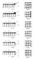
- FIGS. 1A-1Fare diagrammatic sketches in sectional view showing examples of various die edge configurations.
- FIGS. 2A-2Fare diagrammatic sketches in sectional view showing stacks of die having die edge configurations as in FIGS. 1A-1F .
- FIGS. 3A-3Fare diagrammatic sketches in sectional view showing stacks of die having die edge configurations as in FIGS. 1A-1F , in which the respective die are covered by a conformal dielectric coating.
- FIG. 4Ais a diagrammatic sketch in a plan view showing a stack of die according to an embodiment of the invention.
- FIG. 4Bis a diagrammatic sketch showing interconnected stacked die assemblies in a sectional view as indicated at 4 B- 4 B in FIG. 4A .
- FIG. 5is a diagrammatic sketch in a plan view showing a stack of die according to another embodiment of the invention.
- FIG. 6Ais a diagrammatic sketch in a plan view showing interconnection of pads in a stack of die as in FIG. 4A according to an embodiment of the invention.
- FIG. 6Bis a diagrammatic sketch showing interconnected stacked die assemblies in a sectional view as indicated at 6 B- 6 B in FIG. 4A .
- FIG. 7is a diagrammatic sketch in a plan view showing interconnection of pads in a stack of die according to another embodiment of the invention.
- FIG. 8Ais a diagrammatic sketch in a sectional view showing a tiered stack of two interconnected die stack assemblies according to an embodiment of the invention.
- FIG. 8Bis a diagrammatic sketch in a sectional view showing a tiered stack of two interconnected die stack assemblies according to another embodiment of the invention.
- FIGS. 9A-9Care diagrammatic sketches in sectional view showing stages in preparation of a conformally coated stack of die according to an embodiment of the invention.
- FIGS. 10A-10Care diagrammatic sketches in a sectional view showing stages in preparation of a conformally coated stack of die according to another embodiment of the invention.
- FIGS. 11A and 11Bare diagrammatic sketches in sectional view showing conventional wire-bond two-stack assemblies mounted on a substrate.
- FIG. 12is a diagrammatic sketch in a sectional view showing a stacked die assembly mounted onto and electrically interconnected with a substrate according to an embodiment of the invention.
- FIGS. 13A-13Care diagrammatic sketches outlining examples of various die stacking arrangements.
- FIG. 14Ais a diagrammatic sketch in a plan view showing a stack of die according to an embodiment of the invention.
- FIG. 14Bis a diagrammatic sketch showing a interconnected stacked die assembly in a sectional view as indicated at 14 B- 14 B in FIG. 14A .
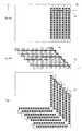
- FIGS. 15Ais a diagrammatic sketch in a partial plan view showing the offset edges of an embodiment of an 8-die offset stack.
- FIG. 15Bis a diagrammatic sketch in a partial sectional view of an 8-die offset stack, as indicated at 15 B- 15 B in FIG. 15A .
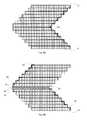
- FIG. 16Ais a diagrammatic sketch in a partial plan view showing the offset edges of an embodiment of an 8-die offset stack, interconnected.
- FIG. 15Bis a diagrammatic sketch in a partial sectional view of an 8-die offset stack, as indicated at 15 B- 15 B in FIG. 15A , interconnected.
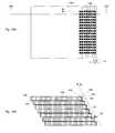
- FIGS. 17 and 18are diagrammatic sketches in partial sectional view of other embodiments of an 8-die offset stack.
- FIG. 19Ais a diagrammatic sketch in a plan view showing a stack of die mounted on a substrate, according to another embodiment of the invention.
- FIGS. 19B and 19Care a diagrammatic sketches showing another embodiment of an interconnected stacked die assembly in a sectional view as indicated at 19 B- 19 B in FIG. 19A .
- FIG. 20Ais a diagrammatic sketch in a plan view showing a stack of die mounted on a substrate, according to another embodiment of the invention.
- FIG. 20Bis a diagrammatic sketch showing another embodiment of an interconnected stacked die assembly in a sectional view as indicated at 20 B- 20 B in FIG. 20A .
- FIG. 21Ais a diagrammatic sketch in a plan view showing a stack of die mounted on a substrate, according to another embodiment of the invention.
- FIG. 21Bis a diagrammatic sketch showing another embodiment of an interconnected stacked die assembly in a sectional view as indicated at 21 B- 21 B in FIG. 21A .
- 21 Cis a diagrammatic sketch showing another embodiment of an interconnected stacked die assembly as in FIG. 21A in an elevational view.
- FIG. 22is a diagrammatic sketch in a plan view showing a stack of die mounted on a substrate, according to another embodiment of the invention.
- FIGS. 23A-23Care diagrammatic sketches in sectional view showing stages in construction of a conformally coated four die stack assembly according to an embodiment of the invention.
- FIGS. 1A-1Fshow examples of various die edge configurations in die to be interconnected according to various embodiments of the invention.
- FIG. 1Ashows a die having an “off-die” interconnect.
- the dieis shown in a partial sectional view, having an active side 15 at which the integrated circuitry 11 of the die is formed, and a die sidewall 19 .
- an interconnect terminal 22is bonded to an interconnect pad (die pad) 13 .
- the die padmay be a peripheral die pad in the die as provided, or it may be situated at or near the die periphery as a result of rerouting of the die circuitry.
- the interconnect terminalmay be, for example, a wire (formed for example in a wire bond operation) or a tab or ribbon (formed for example in a ribbon bond operation).
- the interconnect terminal 22extends outwardly beyond the die edge 19 (hence, “off-die” terminal).
- FIG. 1Bshows a die having a bump or glob 23 of an electrically conductive polymer material deposited onto the die pad 13 .
- the globmay be shaped (as in the example of FIGS. 1A , 1 B, so that it extends toward the die edge, and may extend to the die edge or (as in the example shown) slightly beyond the die edge 19 ; it may be in the shape of a thumb, for example.
- the globmay be formed entirely above the pad, as shown in FIG. 3B .
- the conductive polymer materialmay be, for example, a curable conductive polymer such as a conductive epoxy.
- FIG. 1Cshows a die having an interconnect terminal 24 formed in or at the active side of the die, at or near the margin of the die where the active side 15 of the die meets the die sidewall 19 .
- Such an interconnect terminal at the marginmay be an extension of a die pad, for example, and may be situated at or near the die margin as a result of rerouting of the die circuitry.
- FIG. 1Dshows a die having an interconnect terminal 26 formed in the die sidewall 19 .
- the interconnect terminalmay be connected to the integrated circuitry of the die by attachment of a pad of conductive material to an extension of the die pad, for example, or to rerouting circuitry.
- FIG. 1Eshows a die having an interconnect terminal formed so that it wraps around a chamfer that is formed at the front side die edge (at the intersection of the die sidewall with active side 15 of the die).
- a wraparound terminalhas a terminal portion 27 on the chamfer, and a terminal portion 28 on the die sidewall.
- a similar wraparound terminalmay be formed over the back side die edge (at the intersection of the die sidewall with back side 17 of the die), where no chamfer is present.
- FIG. 1Fshows a die having an interconnect terminal formed so that it wraps around a chamfer that is formed at the front side die edge (at the intersection of the die sidewall with active side 15 of the die), and further around a chamfer that is formed at the back side die edge (at the intersection of the die sidewall with back side 17 of the die).
- Such a wraparound terminalhas a terminal portion 27 on the front edge chamfer, and a terminal portion 28 on the die sidewall, and a terminal portion 29 on the back edge chamfer.
- FIGS. 2A-2Fshow arrangements of die as in, respectively, FIGS. 1A-1F , oriented one over another (in these examples, each having three die in the stack).
- the dieare shown “vertically” arranged; that is, they are aligned generally vertically with respect to an arbitrarily assigned “horizontal” plane of the front or back sides of the die, and, accordingly, they may be vertically interconnected at the vertical stack face, for example using a trace of electrically conductive epoxy.
- FIG. 2Ashows, the off-die terminals project at the stack face, making them available for connection by a variety of methods.
- FIG. 2Bshows, in embodiments where the globs 23 of electrically conductive material extend to or slightly beyond the stack face, the globs are similarly available for connection by a variety of methods.
- FIG. 2Cshows, interconnect terminals 24 in the margin of the active side of the die are beneath the margins of die stacked over them (except that the active side of one of the die is exposed and readily accessible for interconnection).
- FIGS. 2D , 2 E, and 2 Fshow, by contrast, interconnect terminals 26 formed in the die edge 19 ( FIG. 1D ), and wraparound interconnect terminals 27 , 28 ( FIG. 1E ) or 27 , 28 , 29 ( FIG. 1F ) are presented at the stack face for interconnection.
- FIGS. 3A-3Fshow stacked die arranged generally as in FIGS. 2A-2F , respectively.
- each die 32is covered with a conformal insulative coating 34 , having openings 35 over the die pads.
- FIG. 3Ashows a three-die stack of die having off-die terminals 22 . Because the off die interconnect terminals in this example stand above the front side of the die, adjacent die in the stack are separated by a space 33 .
- a spacer(as shown for example between two of the die, at 37 ) may optionally be interposed in the space 33 to support adjacent die; optionally the spacer may be a film adhesive of suitable thickness both to fill the space and to affix the die to one another.
- the off-die interconnect terminals 22are vertically aligned, and are presented at the stack face as indicated by arrows 30 , so that they may be readily interconnected using, for example, a vertically-oriented interconnect, as described generally in U.S. Pat. No. 7,245,021, for example.
- FIG. 3Bshows a three-die stack of die having globs 23 of an electrically conductive polymer material deposited onto the die pad 13 in the example shown here, the glob is formed entirely above the exposed die pad, and does not extend toward the stack face (compare, FIGS. 1A , 2 A.
- the globsstand above the front side of the die, so that adjacent die in the stack are separated by a space 33 and, optionally, a spacer (as shown for example between two of the die, at 37 ) may optionally be interposed in the space 33 to support adjacent die; and optionally the spacer may be a film adhesive of suitable thickness both to fill the space and to affix the die to one another.
- the glob 23 in this exampledoes not extend toward the stack face, it permits access to a portion of the interconnect material (not shown in this FIG.) that intrudes into the space between the die at the die edge, as suggested by the arrows 30 .
- FIG. 3Cshows a three-die stack of die having an interconnect terminal 24 formed in or at the active side of the die, at or near the margin of the die where the active side of the die meets the die sidewall.
- the interconnect terminals 24 of lower die in the stack(that is, all the die except the uppermost die in the stack) are overlain by die stacked over them.
- Interconnection of die in such a stackmay be made by a vertically-oriented interconnect at the stack face, provided that the interconnect intrudes between adjacent die onto the interconnect terminals 24 .
- the interconnect material as applied(such as an electrically conductive epoxy) has some capacity to flow into the space at the margin between adjacent die, to make electrical connection with interconnect terminals in the margin at the active side of the die. This necessitates providing a separation 33 between adjacent die sufficient to permit the intrusion.
- a spacermay optionally be interposed in the space 33 to support adjacent die, as shown for example between two of the die at 37 in each of FIGS. 3A , 3 B, 3 C; and optionally the spacer may be a film adhesive of suitable thickness both to fill the space and to affix the die to one another.
- the spaceris located or sized (e.g., it is made smaller than the die) so that it does not block the interconnect terminals.
- FIGS. 3D , 3 E, and 3 Fshows a three-die stack of die having an interconnect terminal formed in or at the die sidewall and presented at the stack face as shown by the arrows 30 .
- the conformal coatingcovers at least the front side and the back side of the die.
- Such a configurationmay be made by coating the entirety of all surfaces of the die and then forming openings through the coating to expose the underlying interconnect terminals; or such a configuration may be made by coating only the front surface and the back surface of the die, leaving the interconnect terminals uncoated.
- the interconnect terminalsare presented at the stack face, and because the interconnect terminals do not stand above the front side of the die, no space is required between adjacent die in the stack (except for the thickness of the conformal coating). Accordingly, as the FIGs. illustrate, the surface of the coating at the backside of an upper die can rest directly upon the surface of the coating on the front (“active”) side of the adjacent lower die in the stack.
- a conformal coatingmay be formed following stacking, and in some embodiments a conformal coating may be formed following mounting of the die stack onto a support. Openings are formed in the conformal coating at sites on the die or on the support at which electrical interconnection is to be made.
- Stacked die in configurations as shown for example in FIGS. 3D , 3 E, and 3 Fcan be readily interconnected using, for example, a vertically-oriented interconnect.
- the inventionprovides stacked die assemblies having improved stacking arrangements, particularly for die having interconnect terminals situated at the front side of the die, and improved die-to-die interconnection within the stacks. Adjacent die in the stack are offset, and pads on the various die are interconnected using an electrically conductive polymer, such as a conductive epoxy, which is deposited in a pattern constituting traces contacting successive pads.
- an electrically conductive polymersuch as a conductive epoxy
- FIG. 4Ashows in a plan view an arrangement of stacked offset die, each die having interconnect terminals arranged in one margin adjacent a front die edge; and FIG. 4B shows the stack in a sectional view as indicated at 4 B- 4 B in FIG. 4A .
- interconnect terminals 48are in this example situated in a row alongside front die edge 49 .
- the die 42 in this exampleis covered on all surfaces (back surface, front surface, sidewalls) by a conformal coating 44 , provided with openings 45 exposing interconnect pads 48 .
- Successive coated die in the stackmay, as in these examples, rest directly one upon another, such that the coating on the back side of an upper die can contact the coating on the front side of the underlying die.
- a die attach filmmay be laminated onto the back side of one or more of the die.
- the dieare all of the same size, and the pads are located along only one die edge. Accordingly, successive die in the stack are displaced (offset) only in a direction orthogonal to a die edge along which the pads are situated.
- FIG. 5shows in plan view an arrangement of stacked offset die, each die having interconnect terminals arranged in a margin adjacent each of two front die edges having a common die corner.
- interconnect terminals 58 , 58 ′are in this example situated in a row alongside each of front die edges 59 , 59 ′.
- the die in this exampleare covered on all surfaces (back surface, front surface, sidewalls) by a conformal coating, provided with openings exposing interconnect pads 58 , 58 ′.
- Successive coated die in the stackmay rest directly one upon another, such that the coating on the back side of an upper die can contact the coating on the front side of the underlying die.
- a die attach filmmay be laminated onto the back side of one or more of the die.
- Die pads in processed semiconductor wafers as provided, or in singulated diemay not be arranged along one die edge, or along two adjacent die edges.
- the padsmay be arranged in one or two rows near a centerline of the die, for example; or, if arranged along die edges, they may be arranged along two opposite die edges or along all four die edges, for example. Or, whatever the arrangement of pads on the wafer or on the die as provided, they may not be arranged in a suitable manner for a given end use; they may be located in an unsuitable sequence, or at an unsuitable pitch, for example).
- the wafer or die as providedmay be if desired be further processed to reroute the original pads to new pad positions along one die edge or along two die edges, prior to mounting the die in stacks for interconnection according to the invention.
- a wafer as provided, or a singulated diemay optionally have a dielectric layer (such as glass, silicon nitride, polyimide, or a benzcyclobutene (BCB) polymer, for example) formed over the integrated circuitry except over the original die pads.
- a dielectric layersuch as glass, silicon nitride, polyimide, or a benzcyclobutene (BCB) polymer, for example
- BCBbenzcyclobutene
- a dielectric layer(such as glass, silicon nitride, polyimide, or a benzcyclobutene (BCB) polymer, for example) may additionally be formed over the rerouting circuitry except over the new (rerouted) interconnect pads.
- a dielectric layersuch as glass, silicon nitride, polyimide, or a benzcyclobutene (BCB) polymer, for example
- BCBbenzcyclobutene
- the dieare all of the same size; here the pads are located along two adjacent front edges. Accordingly, successive die in the stack are displaced with respect to both die edges along which the pads are situated.
- the die stackhas a greater footprint than a single die, as a result of the horizontal displacement of the die. It may be preferable to minimize the footprint of the stack, and this may be accomplished by reducing the extent of horizontal displacement of the die.
- Each dieneed be displaced only to an extent at least sufficient to expose enough of the area of the pads in the underlying die to permit the interconnect material to make reliable electrical contact with the pads and, accordingly, the extent of displacement, indicated for example at d in the FIGs., is shown greater than necessary.
- the displacementmay be sufficient if at least a fraction of the area of the pads is left uncovered by the overlying die. (See, for example, FIGS.
- the interconnect material as depositedmay not contact the pad over an area great enough to establish a reliable electrical connection when the material is cured. It may be preferred to minimize the extent of displacement, so as to minimize the footprint of the stack.
- the interconnect materialmay be an electrically conductive polymer, such as a polymer filled with particles of an electrically conductive material.
- the materialmay a curable polymer, for example, such as electrically conductive epoxy (for example, as silver filled epoxy); and, the interconnect process may include forming traces of the uncured material in a prescribed pattern and thereafter curing the polymer to secure the electrical contacts with the terminals and the mechanical integrity of the traces between them.
- the interconnect materialmay be an electrically conductive ink.
- the stackmay be supported, for example, at the back side of the lowest of the die in the stack, and the interconnect material may be applied along a trajectory over the pads to be connected and the die surfaces between them.
- the interconnect materialmay be applied using an application tool such as, for example, a syringe or a nozzle. The material exits the tool in a deposition direction generally toward the interconnect terminals, and the tool is moved over the die stack face in a work direction.
- the interconnect materialcan be deposited in a deposition direction (two possible directions for the deposition (i.e., material flow from the tool) are shown: D 1 generally perpendicular to the surface of the interconnect terminal, and D 2 at an angle away from perpendicular) while the tool is moved in a work direction W.
- the materialmay be extruded from the tool in a continuous flow, or, the material may exit the tool dropwise. In some embodiments the material exits the tool as a jet of droplets, and is deposited as dots which coalesce upon or following contact with a stack face surface.
- the deposition directionis generally perpendicular to the die edge surface, and in other embodiments the deposition direction is at an angle off perpendicular to the die edge surface.
- Die stacks having resulting traces of interconnect materialare shown by way of illustration at 62 in FIGS. 6A , 6 B, and at 72 in FIG. 7 . This procedure is repeated to deposit traces connecting all the pads for which electrical interconnection is desired, and following deposition the material is cured. Optionally, a cure or partial cure of the interconnect material may be carried out prior to completion of a trace.
- Assemblies of electrically interconnected stacked diecan optionally be tested prior to further processing.
- Complete assembliescan be mounted on a support, and interconnected die in the stack can be connected with underlying circuitry associated with the support by way of secured electrical contact with the interconnections.
- a printed circuit board or package substratecan be provided, having bond pads arranged at a die attach side to correspond with the ends 61 or 63 of the die stack interconnects.
- the interconnect 62has an end 63 at the margin of the active side of a die at the top (or, if the assembly is inverted, at the bottom) of the assembly, and an end 61 at a back side edge of a die at the bottom (or, if the assembly is inverted, at the top) of the assembly.
- a PCB or substratefor example, can be provided having z-interconnect sites arranged in a manner corresponding to the arrangement of interconnect ends 61 or 63 .
- the assemblycan be mounted on the support for example with the active sides of the die facing toward the substrate, and with the interconnect ends 63 aligned with and contacting the z-interconnect sites; or for example with the back sides of the die facing toward the substrate, and with the interconnect ends 61 aligned with and contacting the z-interconnect sites.
- the assemblycan be mounted with the die oriented perpendicularly to the PCB or substrate, with the interconnect ends 61 aligned with and contacting the z-interconnect sites.
- diecan be stacked on a support, or stacked die assemblies can be mounted on a support prior to interconnection.
- interconnection of the die in the stack and of the underlying circuitry with the dieare carried out at the same time, or concurrently.
- the diemay be all of the same size, as shown in the FIGS. 4A , 4 B, 5 (and 6 A, 6 B, 7 ), but die of different sizes may according to the invention be stacked and interconnected by conductive polymer traces.
- a smaller diemay be stacked on a larger die, with the smaller die situated so that peripheral die pads in the margin near at least one die edge of the larger die are available for interconnection.
- the stack of diemay appear in section as a stepped pyramid; or, the die may be displaced in one direction with respect to a first die edge, but vertically interconnected on another die edge.
- An upper diemay be larger in one dimension (that is, the die may be same width but one longer than the other), or in both directions (that is, one die both wider and longer than the other) than a lower die.
- a 10 ⁇ 10 mm diemay be stacked over a 10 ⁇ 12 mm die having peripheral pads at the shorter edges.
- the smaller dieis situated over the larger die such that the die pads at the narrow ends of the larger die are exposed adjacent two edges of the smaller die.
- a 10 ⁇ 10 mm diemay be stacked over a 12 ⁇ 12 mm die, and situated such that peripheral pads along any one or more (or all four) edges of the larger die are available for interconnection.
- FIGS. 13A-13CVarious examples are shown highly diagrammatically, with details omitted for simplicity, in FIGS. 13A-13C .
- Stacked die assemblies according to the inventionmay have as many die as may be desired, and there may as a matter of mechanical design be no upper limit.
- the illustrated examplesshow seven die in each stack, but assemblies having two or more die in the stack are contemplated. Particularly, for example, assemblies having four, or six, or eight, or 9, or 16 or 17 die may be made in the manner illustrated in FIGS. 6B or 7 .
- a stack of 9 diemay include 8 memory die and a controller die.
- larger stacked die assembliesmay be made by constructing stacked die units in a modular design, and then stacking units, as illustrated for example in FIGS. 8A , 8 B.
- an assembly as shown for example in FIG. 6Bmay constitute a modular unit; and a second similar modular unit may be inverted and mounted over it, with the interconnect ends 63 of the respective modular units aligned and connected.
- a resulting assemblyis shown by way of example in FIG. 8A .
- a third modular unitmay be mounted over the two-unit assembly to form a three-unit assembly, with the interconnect ends 61 of the third unit aligned and connected with the interconnect ends 61 at one edge of the two-unit assembly.
- a spacermay be provided between the stacked modular units in an assembly as shown in FIG. 8A .
- the first and second modular unitsare identical, when the second unit is inverted the respective rows of pads at the interconnect ends 63 are antiparallel; that is, a first interconnect on the first unit is now aligned with a last interconnect on the second die.
- rerouting circuitrymay be required, to connect the appropriate respective features 61 , 63 .
- Rerouting circuitrymay be provided at the active side the top die of the first unit; or, where a spacer is included, the spacer may constitute an interposer, including one or more dielectric layers and one or more conductive rerouting layers.
- an assembly as shown for example in FIG. 6Bmay constitute a modular unit; and a second similar modular unit may be mounted over it, but not inverted.
- An interposerincluding at least one dielectric layer 86 (such as glass, for example) and at least one patterned conductive layer 84 is situated between the modular units, to provide rerouting from the interconnect ends 63 on one edge of the first unit to the interconnect ends 61 on the (oppositely situated) edge of the second unit.
- a resulting assemblyis shown by way of example in FIG. 8B .
- a third modular unitmay be mounted over the two-unit assembly to form a three-unit assembly, with an interposer situated between successive stacked units.
- the stackable modular unitscan be robust and testable.
- particular two-die units and four die unitsmay constitute modules; from these modules a six-die assembly may be made by stacking a two-die unit and a four-die unit, or an eight-die assembly may be made by stacking two four-die units, for example.
- the die as providedmay have a dielectric layer over the front side (except over the interconnect pads, which are exposed for interconnection), and for such die electrical insulation between adjacent die in the stack, as would be provided by the conformal die coating, is unnecessary. That is, the die as provided or as rerouted, insulated with a dielectric layer over the front side, may be stacked one directly upon another in an offset configuration, as shown for example in FIG. 9A . A completed assembly of such die in a stack may be provided with a conformal coating, resulting in a coated stacked die assembly, as shown for example in FIG.
- such a stackmay be mounted on a support such as a substrate or printed circuit board or leadframe prior to coating; in such embodiments the coating may cover exposed areas of the support as well.
- a thin space between adjacent diemay admit the conformal coating material, providing for electrical insulation between adjacent die (if the space is sufficiently thick), as well as adhesion of adjacent die in the stack.
- Such a spacemay be provided by placing spacers over the component, and then stacking the overlying adjacent component onto the spacers, as described for example in U.S. Provisional Application No. 60/971,203, the pertinent portions of which are hereby incorporated herein by reference.
- the spacershave nominally the same height, to provide a standoff between overlying adjacent components in a range, for example, about 1 um to about 5 um. This is described below in further detail with reference to FIGS. 23A-23C . Openings through the conformal coating are then formed to expose interconnect pads, resulting in a stack of die, as shown for example in FIG. 9C , ready for interconnection generally as described above with reference to FIGS. 4A , 4 B, 5 and 6 A, 6 B, 7 . Or, a configuration as in FIG. 9C may result from applying a conformal coating to all surfaces of each die, and thereafter stacking the die in an offset configuration; in such embodiments openings may be made over the interconnect pads either prior to or following stacking the die.
- an electrically insulative adhesivemay be applied between adjacent uncoated die in the stack.
- the adhesivemay be a curable dielectric polymer for example, such as a die attach epoxy; this may be applied onto a surface of one of the die and then the die put together to form a uniform adhesive layer between them.
- the adhesivemay be an epoxy preform or dielectric film adhesive (die attach film); this may be applied to a surface of one of the die, and the die may be mounted together. Where a dielectric film adhesive is used, it may be applied at the wafer level or at the die array level, and cut to size on the die during die singulation or separation. FIG.
- FIG. 10Ashows a completed assembly of die having a film adhesive (e.g., 102 ) between successive die in the stack.
- a film adhesivee.g., 102
- completed assembly of such die in a stack as in FIG. 10Amay be provided with a conformal coating, resulting in a coated stacked die assembly, as shown for example in FIG. 10B .
- Openings through the conformal coatingare then formed to expose interconnect pads, resulting in a stack of die, as shown for example in FIG. 10C , ready for interconnection generally as described above with reference to FIGS. 4A , 4 B, 5 and 6 A, 6 B, 7 .
- Stacked die units or assemblies constructed according to the inventioncan be electrically interconnected with circuitry in a device for use.
- a stacked die unitcan be mounted upon the active side of another die, and electrically interconnected by connection of all or selected ones of the interconnect ends of the unit with pads on the die.
- a die stack assemblycan be mounted on a support having electrical interconnection sites (such as a package substrate or a leadframe, or a printed circuit board, for example), and electrically interconnected by connection of all or selected ones of the interconnect ends of the unit with sites in the substrate.
- FIG. 12is a diagrammatic sketch illustrating a way in which die stacking and electrical interconnect according to embodiments of the invention can provide for a smaller assembly footprint as compared to conventional die stacking and wire bond interconnection.
- FIG. 11shows a two-die stack having a smaller die 126 stacked over a larger die 122 , and mounted on a substrate 110 .
- Die 122is affixed to the substrate by a film adhesive 142 ; and die 126 is affixed to the die 122 by a film adhesive 144 .
- Die 122is electrically connected by wire bonds 114 connected to die pads 124 on die 122 and to bond sites 112 on bond pads 111 on the substrate; die 126 is electrically connected by wire bonds 116 connected to die pads 128 on die 126 and to die pads 124 on die 122 .
- the widths of the wire spansare indicated by dimensions s, s′ in FIG. 11A .
- the wire span dimensionmust be great enough to accommodate the movement of the wire bonding tool during the wire bond process, and to provide clearance for the wire at the die edge.
- FIG. 11Bshows a two-die stack having similarly-dimensioned die 120 , 120 ′ stacked in an offset arrangement, with die pads along one edge of each die.
- the die 120 , 120 ′are affixed to the feature beneath (die or substrate) using a film adhesive 122 , 122 ′.
- Die 120is electrically connected by wire bonds connected to die pads on die 120 ′ and to bond sites on bond pads 111 on the substrate; die 120 ′ is electrically connected by wire bonds connected to die pads on die 120 ′ and to die pads on die 120 .
- the widths of the wire spansare indicated by dimensions w, w′ in FIG. 11B .
- the opposite edge of the die 120 ′overhangs the opposite edge of the die 120 as indicated by dimension h in FIG. 11B ; where, as in this example, the die are the same size, the dimension h is the same as the die offset, which is contributed to by the wire span w and the distance between the interconnect sites on the die and the die edge.
- a two-die assembly interconnected as in some embodiments of the inventionis mounted onto and connected to a substrate 410 .
- the dieare provided with a conformal electrically insulative coating, and are stacked and interconnected using, for example, an electrically conductive polymer, generally as described above with reference to FIG. 4A , for example.
- the die 420 , 420 ′are offset by a distance indicated at o in FIG. 12 , which (for die having similar dimensions) approximates the offset s
- the offset (displacement) of the dieneed be great enough to expose an area of the underlying pads sufficient to provide reliable electrical connections on the pads.
- the interconnectionmust satisfy the resistance requirements of the circuit, and, as may be appreciated, the size of the area will depend among other factors upon the materials employed and the contact resistance, as well as the requirements of the circuitry.
- the width s′ of the area on the substrate where the lowest die in the stack is interconnected with the substrateneed not be greater than the bond site dimension on the substrate.
- the minimum practical die offset in stacked die interconnected according to embodiments of the inventioncan be in a range approximately one-third to as much as one-eighth the minimum practical offset die for similarly-dimensioned stacked die interconnected by conventional wire bonding.
- an interconnect span for a stack of similarly-dimensioned die according to the inventioncan be about 50 um-100 um in some embodiments.
- the offsetmay be such that only a portion of the area of the pads is exposed at the edge of an overhanging die.
- FIGS. 14A , 14 Bshow in a plan view an arrangement of stacked offset die, each die having interconnect terminals arranged in one margin adjacent a front die edge; and FIG. 14B shows the stack in a sectional view as indicated at 14 B- 14 B in FIG. 14A .
- interconnect terminals 148are in this example situated in a row alongside front die edge 149 .
- the die 142 in this exampleis covered on all surfaces (back surface, front surface, sidewalls) by a conformal coating 144 , provided with openings 145 exposing interconnect pads 148 .
- Successive coated die in the stackmay, as in these examples, rest directly one upon another, such that the coating on the back side of an upper die can contact the coating on the front side of the underlying die.
- a die attach filmmay be laminated onto the back side of one or more of the die.
- the dieare all of the same size, and the pads are located along only one die edge. Accordingly, successive die in the stack are displaced (offset) only in a direction orthogonal to a die edge along which the pads are situated.
- the die stackhas a greater footprint than a single die, as a result of the horizontal displacement of the die.
- the footprint of the stackhas been reduced, by reducing the extent of horizontal displacement of the die so that each die is displaced only to an extent at least sufficient to expose enough of the area of the pads in the underlying die to permit the interconnect material to make reliable electrical contact with the pads.
- the extent of displacementindicated for example at d in the FIGs., leaves a fraction of the area of the pads uncovered by the overlying die.
- FIGS. 15A , 15 Bthere is shown in more detail the interconnect region of an 8-die offset stack.
- the stackis mounted on a support (here a substrate) 151 having interconnect sites (leads) 150 .
- the stack edgeoverlaps the interconnect sites on the substrate, so there is no interconnect span dimension next to the stack.
- the die in this exampleare each covered on all sides with a conformal insulative coating (in this example a parylene). Openings through the conformal coating were made in each die to expose selected interconnect terminals 158 , while leaving selected other interconnect terminal protected (insulated).
- FIGS. 16A , 16 Bshow an 8-die offset stack electrically interconnected with interconnect traces 160 . The traces electrically connect exposed interconnect terminals 158 to a corresponding interconnect site 150 on the substrate 151 .
- the interconnect materialis formed by stencil printing, and this technique may be particularly useful for interconnecting offset die stacks.
- a stencil having suitable openingsmay be aligned over the stack, and the interconnect material may be passed through the openings to the stacked offset die edges beneath.
- the vertical elevation of the stencil above the supportmay be low enough so that the interconnect material is directed accurately to the interconnect terminals and the interconnect sites on the support.
- the conformal coatingmay be applied at any of various stages in the process.
- the diewere stacked, with spacers between adjacent die to permit the coating material to form between the die; then the conformal insulative coating 174 was formed (in this example a parylene); and then openings were formed to expose selected interconnect terminals 178 .
- the stackis shown mounted on a substrate, generally as in FIG. 16A .
- the coating processcan be carried out following mounting the stack on the substrate and, in such embodiments, exposed surfaces of the substrate are also coated, and openings must be made in the corresponding interconnect sites on the substrate as well.
- the interconnect tracesare formed, generally as shown in FIGS. 16A , 16 B.
- the diewere coated before stacking, as shown in FIGS. 15A , 15 B; here, however, the coated die were stacked and mounted on the substrate; and then openings were formed in the coating 184 (here a parylene) to expose selected interconnect terminals 188 .
- the interconnect tracesare formed, generally as shown in FIGS. 16A , 16 B.
- FIGS. 19A , 19 Bshow another embodiment of a stacked die assembly, in which adjacent offset die in the stack are mounted one over another so that respective interconnect edges are vertically aligned.
- vertically adjacent dieare referred to as a “pair” of die, although they need not be functionally related as a pair nor handled as a pair during processing.
- the die in each pairfor example the top pair of die 191 , 192 , are oppositely oriented, so that the interconnect edges 193 and 194 are at opposite sides of the stack.
- the arrangementis shown in further detail in FIG. 19C .
- die 191is stacked over die 192 constituting a first (top) die pair.
- the interconnect margin 193 of die 191is oriented toward the right in the FIG., and the interconnect margin 194 of die 192 is oriented toward the left.
- the dieare offset so that the interconnect terminals of interconnect margin 194 is exposed.
- the interconnect terminals 195 , 196are each provided with a glob or knob of conductive material 197 , 198 , to provide contact access for columns 201 , 202 of interconnect material formed at the sides.
- each interconnect margin 193 , 194 of the first pair of die 191 , 192overhang the interconnect margin of the pair of die beneath; thus, interconnect margins 193 , 194 of the first pair of die 191 , 192 overhang interconnect margins 193 ′, 194 ′ of the next pair of die 191 ′, 192 ′.
- the configuration at each set of marginsis similar to that of the construct shown in FIG. 3B , but in this construct the (even numbered) die 192 , 192 ′ serve as spacers for the (odd numbered) die 191 , 191 ′ (see spacer 37 between two of the die in FIG. 3B ).
- the stack of dieare mounted on a support (here, substrate 200 ) so that the die edges overlap corresponding interconnect sites 203 , 204 in the substrate.
- interconnect traces 201 , 202are formed, contacting the knobs (e.g., 197 , 198 ) at the die and contacting the sites 203 , 204 in the substrate.
- the interconnect trace 202provides electrical continuity between site 204 and circuitry on die 192 , 192 ′, 192 ′′, 192 ′′′; and the interconnect trace 203 provides electrical continuity between site 203 and circuitry on die 191 , 191 ′, 191 ′′, 191 ′′′.
- the knobmay be a metal bump, for example, such as a stud bump formed of gold using a wire bonding tool; or, the knob may be a solder bump, which may be formed as a deposit of a solder paste, for example, which may be formed by printing or dispensing; or, the knob may be metal, formed for example in a plating process; or, the knob may be a deposit of an electrically conductive polymer.
- the materialcan include any of the various materials that are suitable for the interconnect trace material itself, and can be formed by, for example, any of the techniques described for forming the interconnect traces, as described above.
- Interconnect materials suitable for the traces 201 , 202include, for example, curable conductive polymers such as conductive epoxies. Because the interconnect traces in these embodiments are not externally supported between the interconnect sites on the substrate and the die, or between the spaced-apart die, the interconnect material must be sufficiently firm in the uncured state to maintain the columnar shape and the contact with the knobs or globs. Suitable polymers have a high thixotropic index, usually 6.5 or greater; and a high viscosity, usually 30,000 cps or greater.
- Formation of the columnsmay be made by a pulse dispense procedure, as described in U.S. application Ser. No. 12/124,097, (cited above).
- all the diemay be designed with a first set of pads (numbered, for example, #1-#32) along one margin and a second set of pads (numbered #32-#1) along the opposite margin.
- FIGS. 20A , 20 Bshow such an embodiment.
- the dieare constructed generally as shown in FIGS. 19A , 19 B, with a second set of pads 295 , 296 along the margin opposite the interconnect margin. It is unnecessary to rotate successive die; rather, the die are mounted all in the same orientation, and, following coating, the unneeded sets of pads can be left unexposed.
- FIGS. 21A , 21 B, 21 CA further stacking arrangement is shown in the embodiment shown in FIGS. 21A , 21 B, 21 C.
- the dieare longer in an X-direction than in a Y-direction, and the interconnect terminal are situated in the margins along the shorter edges.
- Successive die in the stackare oriented at right angles to the die stacked over or under.
- Interconnectionis carried out generally as described with reference to FIG. 19C : the interconnect traces are formed as columns 212 , 214 , and, e.g., 216 connecting the interconnect terminals on the overhanging die, and the die pads are provided with globs or knobs (not shown in these FIGs.) to which the columns make electrical contact.
- the even numbered dieserve as spacers for the odd numbered die.
- FIG. 22Still another embodiment of a stacked die configuration is shown by way of example in FIG. 22 .
- Reference is made to FIG. 5showing stacked offset die, each die having interconnect terminals arranged in a margin adjacent each of two front die edges having a common die corner.
- successive dieare offset to expose the pads (or part of the pads) in the underlying die.
- pairs of offset die in the stackare mounted one over another so that the respective interconnect edges are vertically aligned.
- one die in each pairis oriented at 180° with respect to the other. Interconnection is carried out generally as described with reference to FIG.
- the interconnect traces(not shown in this FIG.) are formed as columns connecting the interconnect terminals on the overhanging die, and the die pads are provided with globs or knobs (not shown in these FIGs.) to which the columns make electrical contact.
- the even numbered dieserve as spacers for the odd numbered die.
- uncoated diemay be stacked and then a coating process may be applied to the stack.
- a paryleneis formed using a dry vapor deposition
- the active monomercondenses on surfaces within very small spaces and, accordingly, the polymer can form in a very thin space between adjacent die.
- Such a very thin layer of polymercan suffice to effect adhesion between adjacent die.
- FIG. 23Ashows four die 2312 , 2312 ′, 2312 ′′, 2312 ′′′, selected 2320 for assembly into a four-die stack.
- Each die except the topmost one in the stackis provided with (in this example) a number of generally spheroidal spacer elements 2314 all having approximately the same nominal height.
- the material of the spacer elementsis electrically nonconductive.
- the spacer elementsmay have a nominal height in a range about 5 um to about 40 um, for example.
- the assembly of spaced-apart dieis then subjected to a conformal coating process, resulting in a coated stacked die assembly 2324 , as shown in FIG. 23C .
- the coating 2316forms on all exposed surfaces of the assembly, including a die active side at the “top” of the stack, a die backside at the “bottom” of the stack, and die sidewalls; and including the spaced-apart front sides and back sides of adjacent die in the stack, as indicated at 2317 .
- the individual dieare provided prior to stacking and adhesion with a conformal coating over at least a contact area; the coated die are stacked to form an assembly of coated die; and the assembly of coated die is subjected to a further conformal coating process to encapsulate the stack and, optionally, to effect adhesion of the die in the stack and/or the stack to an additional stack or to a non-die support.
- a greater or lesser number of spacer elementsmay be required to provide adequate support, depending for example upon the flexibility of the die (thinner die may require more support) and upon the height of the stack and the number of die in the stack.
- the spacer elementsmay be, for example, glass or nonconductive polymer spheres; and they may be scattered over the surface of each die.
- the spacersmay be small polymer dots, which may be adhesive to some extent (they may be a polymer adhesive, for example an epoxy) to affix the adjacent die temporarily, so that the die in the stack do not shift during processing steps leading up to the completion of the conformal coating over the stack; and they may be printed (for example screen printed or mask printed) onto the die surface, or dispensed onto the die surface using a needle or nozzle, for example.
- the coatingneed be situated only within an area where contact of the surface of the coated die and the surface of the substrate is expected.
- the coatingmay be only within the die attach area of the die.
- FIGS. 13A through 13Care illustrative of additional stacked die assemblies in which advantages of aspects of the invention may be had.
Landscapes
- Engineering & Computer Science (AREA)
- Microelectronics & Electronic Packaging (AREA)
- Power Engineering (AREA)
- Computer Hardware Design (AREA)
- Physics & Mathematics (AREA)
- Condensed Matter Physics & Semiconductors (AREA)
- General Physics & Mathematics (AREA)
- Manufacturing & Machinery (AREA)
- Encapsulation Of And Coatings For Semiconductor Or Solid State Devices (AREA)
- Internal Circuitry In Semiconductor Integrated Circuit Devices (AREA)
- Lead Frames For Integrated Circuits (AREA)
Abstract
Description
Claims (38)
Priority Applications (9)
| Application Number | Priority Date | Filing Date | Title |
|---|---|---|---|
| US12/124,077US8723332B2 (en) | 2007-06-11 | 2008-05-20 | Electrically interconnected stacked die assemblies |
| KR1020107000565AKR101522745B1 (en) | 2007-06-11 | 2008-06-04 | Electrically interconnected stacked die assemblies |
| PCT/US2008/065793WO2008154255A2 (en) | 2007-06-11 | 2008-06-04 | Electrically interconnected stacked die assemblies |
| TW97121195ATWI469303B (en) | 2007-06-11 | 2008-06-06 | Electrically interconnected stacked die assemblies |
| TW097134551ATWI529866B (en) | 2007-09-10 | 2008-09-09 | Semiconductor die mount by conformal die coating |
| US12/913,604US8629543B2 (en) | 2007-06-11 | 2010-10-27 | Electrically interconnected stacked die assemblies |
| US13/109,996US9153517B2 (en) | 2008-05-20 | 2011-05-17 | Electrical connector between die pad and z-interconnect for stacked die assemblies |
| US14/480,373US20150056753A1 (en) | 2008-05-20 | 2014-09-08 | Semiconductor Die Having Fine Pitch Electrical Interconnects |
| US14/871,185US9508689B2 (en) | 2008-05-20 | 2015-09-30 | Electrical connector between die pad and z-interconnect for stacked die assemblies |
Applications Claiming Priority (4)
| Application Number | Priority Date | Filing Date | Title |
|---|---|---|---|
| US94325207P | 2007-06-11 | 2007-06-11 | |
| US97090307P | 2007-09-07 | 2007-09-07 | |
| US98145707P | 2007-10-19 | 2007-10-19 | |
| US12/124,077US8723332B2 (en) | 2007-06-11 | 2008-05-20 | Electrically interconnected stacked die assemblies |
Related Child Applications (1)
| Application Number | Title | Priority Date | Filing Date |
|---|---|---|---|
| US12/913,604DivisionUS8629543B2 (en) | 2007-06-11 | 2010-10-27 | Electrically interconnected stacked die assemblies |
Publications (2)
| Publication Number | Publication Date |
|---|---|
| US20080303131A1 US20080303131A1 (en) | 2008-12-11 |
| US8723332B2true US8723332B2 (en) | 2014-05-13 |
Family
ID=40095081
Family Applications (2)
| Application Number | Title | Priority Date | Filing Date |
|---|---|---|---|
| US12/124,077Active2031-01-19US8723332B2 (en) | 2007-06-11 | 2008-05-20 | Electrically interconnected stacked die assemblies |
| US12/913,604ActiveUS8629543B2 (en) | 2007-06-11 | 2010-10-27 | Electrically interconnected stacked die assemblies |
Family Applications After (1)
| Application Number | Title | Priority Date | Filing Date |
|---|---|---|---|
| US12/913,604ActiveUS8629543B2 (en) | 2007-06-11 | 2010-10-27 | Electrically interconnected stacked die assemblies |
Country Status (4)
| Country | Link |
|---|---|
| US (2) | US8723332B2 (en) |
| KR (1) | KR101522745B1 (en) |
| TW (1) | TWI469303B (en) |
| WO (1) | WO2008154255A2 (en) |
Cited By (21)
| Publication number | Priority date | Publication date | Assignee | Title |
|---|---|---|---|---|
| US20130020720A1 (en)* | 2011-07-18 | 2013-01-24 | Young Lyong Kim | Semiconductor packages and methods of forming the same |
| US20130241050A1 (en)* | 2012-03-14 | 2013-09-19 | Mellanox Technologies Ltd. | Integrated optoelectronic interconnects with side-mounted transducers |
| US8867870B2 (en) | 2012-02-05 | 2014-10-21 | Mellanox Technologies Ltd. | Optical module fabricated on folded printed circuit board |
| US8870467B2 (en) | 2012-05-06 | 2014-10-28 | Mellanox Technologies Ltd. | Optical interface and splitter with micro-lens array |
| US20150014860A1 (en)* | 2013-07-11 | 2015-01-15 | Samsung Electronics Co., Ltd. | Semiconductor chip connecting semiconductor package |
| US20160086904A1 (en)* | 2010-02-22 | 2016-03-24 | Interposers Gmbh | Method and a System for Producing a Semi-Conductor Module |
| US9323014B2 (en) | 2012-05-28 | 2016-04-26 | Mellanox Technologies Ltd. | High-speed optical module with flexible printed circuit board |
| US9490195B1 (en) | 2015-07-17 | 2016-11-08 | Invensas Corporation | Wafer-level flipped die stacks with leadframes or metal foil interconnects |
| US9508691B1 (en) | 2015-12-16 | 2016-11-29 | Invensas Corporation | Flipped die stacks with multiple rows of leadframe interconnects |
| US9583426B2 (en) | 2014-11-05 | 2017-02-28 | Invensas Corporation | Multi-layer substrates suitable for interconnection between circuit modules |
| US9595511B1 (en) | 2016-05-12 | 2017-03-14 | Invensas Corporation | Microelectronic packages and assemblies with improved flyby signaling operation |
| US9728524B1 (en) | 2016-06-30 | 2017-08-08 | Invensas Corporation | Enhanced density assembly having microelectronic packages mounted at substantial angle to board |
| US9825002B2 (en) | 2015-07-17 | 2017-11-21 | Invensas Corporation | Flipped die stack |
| US9837394B2 (en) | 2015-12-02 | 2017-12-05 | International Business Machines Corporation | Self-aligned three dimensional chip stack and method for making the same |
| US9871019B2 (en) | 2015-07-17 | 2018-01-16 | Invensas Corporation | Flipped die stack assemblies with leadframe interconnects |
| US20180145053A1 (en)* | 2016-11-22 | 2018-05-24 | Samsung Electronics Co., Ltd. | Semiconductor package and method of manufacturing the same |
| US10083909B2 (en) | 2015-12-14 | 2018-09-25 | Invensas Corporation | Embedded vialess bridges |
| US10283492B2 (en) | 2015-06-23 | 2019-05-07 | Invensas Corporation | Laminated interposers and packages with embedded trace interconnects |
| US10566310B2 (en) | 2016-04-11 | 2020-02-18 | Invensas Corporation | Microelectronic packages having stacked die and wire bond interconnects |
| US11721671B2 (en) | 2020-07-17 | 2023-08-08 | Samsung Electronics Co., Ltd. | Semiconductor package |
| US20240079369A1 (en)* | 2022-09-06 | 2024-03-07 | Micron Technology, Inc. | Connecting semiconductor dies through traces |
Families Citing this family (126)
| Publication number | Priority date | Publication date | Assignee | Title |
|---|---|---|---|---|
| US6900528B2 (en)* | 2001-06-21 | 2005-05-31 | Micron Technology, Inc. | Stacked mass storage flash memory package |
| US7426780B2 (en) | 2004-11-10 | 2008-09-23 | Enpirion, Inc. | Method of manufacturing a power module |
| US7688172B2 (en) | 2005-10-05 | 2010-03-30 | Enpirion, Inc. | Magnetic device having a conductive clip |
| US8631560B2 (en) | 2005-10-05 | 2014-01-21 | Enpirion, Inc. | Method of forming a magnetic device having a conductive clip |
| US8701272B2 (en) | 2005-10-05 | 2014-04-22 | Enpirion, Inc. | Method of forming a power module with a magnetic device having a conductive clip |
| US8139362B2 (en) | 2005-10-05 | 2012-03-20 | Enpirion, Inc. | Power module with a magnetic device having a conductive clip |
| US8723332B2 (en) | 2007-06-11 | 2014-05-13 | Invensas Corporation | Electrically interconnected stacked die assemblies |
| WO2008157722A1 (en)* | 2007-06-19 | 2008-12-24 | Vertical Circuits, Inc. | Wafer level surface passivation of stackable integrated circuit chips |
| JP5049684B2 (en)* | 2007-07-20 | 2012-10-17 | 新光電気工業株式会社 | Multilayer semiconductor device and manufacturing method thereof |
| US7880309B2 (en)* | 2007-07-30 | 2011-02-01 | Qimonda Ag | Arrangement of stacked integrated circuit dice having a direct electrical connection |
| US7920042B2 (en) | 2007-09-10 | 2011-04-05 | Enpirion, Inc. | Micromagnetic device and method of forming the same |
| WO2009035849A2 (en) | 2007-09-10 | 2009-03-19 | Vertical Circuits, Inc. | Semiconductor die mount by conformal die coating |
| US8133529B2 (en) | 2007-09-10 | 2012-03-13 | Enpirion, Inc. | Method of forming a micromagnetic device |
| CN101999167B (en)* | 2008-03-12 | 2013-07-17 | 伊文萨思公司 | Support mounted electrically interconnected die assembly |
| US7863159B2 (en) | 2008-06-19 | 2011-01-04 | Vertical Circuits, Inc. | Semiconductor die separation method |
| US8829677B2 (en)* | 2010-10-14 | 2014-09-09 | Invensas Corporation | Semiconductor die having fine pitch electrical interconnects |
| US9153517B2 (en)* | 2008-05-20 | 2015-10-06 | Invensas Corporation | Electrical connector between die pad and z-interconnect for stacked die assemblies |
| US8266793B2 (en)* | 2008-10-02 | 2012-09-18 | Enpirion, Inc. | Module having a stacked magnetic device and semiconductor device and method of forming the same |
| US8153473B2 (en) | 2008-10-02 | 2012-04-10 | Empirion, Inc. | Module having a stacked passive element and method of forming the same |
| US9054086B2 (en)* | 2008-10-02 | 2015-06-09 | Enpirion, Inc. | Module having a stacked passive element and method of forming the same |
| US8339802B2 (en) | 2008-10-02 | 2012-12-25 | Enpirion, Inc. | Module having a stacked magnetic device and semiconductor device and method of forming the same |
| KR20100049283A (en)* | 2008-11-03 | 2010-05-12 | 삼성전자주식회사 | Semiconductor package and method for manufacturing of the same |
| JP5126002B2 (en)* | 2008-11-11 | 2013-01-23 | セイコーエプソン株式会社 | Semiconductor device and manufacturing method of semiconductor device |
| JP5700927B2 (en)* | 2008-11-28 | 2015-04-15 | 新光電気工業株式会社 | Semiconductor device and manufacturing method of semiconductor device |
| JP2010165984A (en)* | 2009-01-19 | 2010-07-29 | Toshiba Corp | Semiconductor device |
| EP2251454B1 (en) | 2009-05-13 | 2014-07-23 | SiO2 Medical Products, Inc. | Vessel coating and inspection |
| US8097956B2 (en)* | 2009-03-12 | 2012-01-17 | Apple Inc. | Flexible packaging for chip-on-chip and package-on-package technologies |
| WO2013170052A1 (en) | 2012-05-09 | 2013-11-14 | Sio2 Medical Products, Inc. | Saccharide protective coating for pharmaceutical package |
| WO2010151578A2 (en)* | 2009-06-26 | 2010-12-29 | Vertical Circuits, Inc. | Electrical interconnect for die stacked in zig-zag configuration |
| US7816181B1 (en)* | 2009-06-30 | 2010-10-19 | Sandisk Corporation | Method of under-filling semiconductor die in a die stack and semiconductor device formed thereby |
| US9458536B2 (en) | 2009-07-02 | 2016-10-04 | Sio2 Medical Products, Inc. | PECVD coating methods for capped syringes, cartridges and other articles |
| US8664748B2 (en)* | 2009-08-17 | 2014-03-04 | Mosaid Technologies Incorporated | Package-level integrated circuit connection without top metal pads or bonding wire |
| KR101563630B1 (en)* | 2009-09-17 | 2015-10-28 | 에스케이하이닉스 주식회사 | Semiconductor package |
| WO2011056668A2 (en)* | 2009-10-27 | 2011-05-12 | Vertical Circuits, Inc. | Selective die electrical insulation additive process |
| TWI544604B (en) | 2009-11-04 | 2016-08-01 | 英維瑟斯公司 | Stacked die assembly having reduced stress electrical interconnects |
| US20110147069A1 (en)* | 2009-12-18 | 2011-06-23 | International Business Machines Corporation | Multi-tiered Circuit Board and Method of Manufacture |
| US9367462B2 (en)* | 2009-12-29 | 2016-06-14 | Empire Technology Development Llc | Shared memories for energy efficient multi-core processors |
| JP5512292B2 (en)* | 2010-01-08 | 2014-06-04 | ルネサスエレクトロニクス株式会社 | Manufacturing method of semiconductor device |
| KR101685057B1 (en)* | 2010-01-22 | 2016-12-09 | 삼성전자주식회사 | Stacked package of semiconductor device |
| KR101096042B1 (en) | 2010-03-18 | 2011-12-19 | 주식회사 하이닉스반도체 | Semiconductor package and manufacturing method thereof |
| KR101096271B1 (en) | 2010-04-21 | 2011-12-22 | 주식회사 하이닉스반도체 | Semiconductor package having a structure of package on package and method of fabricating the same |
| US11624115B2 (en) | 2010-05-12 | 2023-04-11 | Sio2 Medical Products, Inc. | Syringe with PECVD lubrication |
| JP5433506B2 (en)* | 2010-06-17 | 2014-03-05 | ラピスセミコンダクタ株式会社 | Semiconductor memory device |
| US8464107B2 (en)* | 2010-06-28 | 2013-06-11 | Qualcomm Incorporated | Surrogate circuit for testing an interface |
| KR101640832B1 (en)* | 2010-07-16 | 2016-07-19 | 삼성전자주식회사 | stacked Semiconductor Package and Method of fabricating the same |
| US8373280B2 (en)* | 2010-09-01 | 2013-02-12 | Oracle America, Inc. | Manufacturing fixture for a ramp-stack chip package using solder for coupling a ramp component |
| US8283766B2 (en)* | 2010-09-02 | 2012-10-09 | Oracle America, Inc | Ramp-stack chip package with static bends |
| TWI411090B (en)* | 2010-11-05 | 2013-10-01 | 矽品精密工業股份有限公司 | Multi-chip stack package structure |
| US9878101B2 (en) | 2010-11-12 | 2018-01-30 | Sio2 Medical Products, Inc. | Cyclic olefin polymer vessels and vessel coating methods |
| CN102468278B (en)* | 2010-11-15 | 2014-02-12 | 矽品精密工业股份有限公司 | Multi-chip stack package structure |
| US8587088B2 (en) | 2011-02-17 | 2013-11-19 | Apple Inc. | Side-mounted controller and methods for making the same |
| JP5289484B2 (en)* | 2011-03-04 | 2013-09-11 | 株式会社東芝 | Manufacturing method of stacked semiconductor device |
| WO2012126379A1 (en)* | 2011-03-23 | 2012-09-27 | Nantong Fujitsu Microelectronics Co., Ltd. | Three-dimensional system-level packaging methods and structures |
| US9272095B2 (en) | 2011-04-01 | 2016-03-01 | Sio2 Medical Products, Inc. | Vessels, contact surfaces, and coating and inspection apparatus and methods |
| US8966747B2 (en) | 2011-05-11 | 2015-03-03 | Vlt, Inc. | Method of forming an electrical contact |
| KR20120135626A (en)* | 2011-06-07 | 2012-12-17 | 삼성전자주식회사 | Method for manufacturing semiconductor chip package |
| EP2726294B1 (en) | 2011-06-29 | 2018-10-17 | Hewlett-Packard Development Company, L.P. | Piezoelectric inkjet die stack |
| US8733893B2 (en) | 2011-07-29 | 2014-05-27 | Hewlett-Packard Development Company, L.P. | Multi-member, nested printhead |
| KR101887084B1 (en) | 2011-09-22 | 2018-08-10 | 삼성전자주식회사 | Multi-chip semiconductor package and method of forming the same |
| KR20130042267A (en)* | 2011-10-18 | 2013-04-26 | 삼성전자주식회사 | Semiconductor package and method of manufacturing the same |
| CA2855353C (en) | 2011-11-11 | 2021-01-19 | Sio2 Medical Products, Inc. | Passivation, ph protective or lubricity coating for pharmaceutical package, coating process and apparatus |
| US11116695B2 (en) | 2011-11-11 | 2021-09-14 | Sio2 Medical Products, Inc. | Blood sample collection tube |
| TWI506801B (en)* | 2011-12-09 | 2015-11-01 | Hon Hai Prec Ind Co Ltd | Solar battery pack |
| CN103165690B (en) | 2011-12-16 | 2015-11-25 | 清华大学 | Solar cell |
| CN103165719B (en) | 2011-12-16 | 2016-04-13 | 清华大学 | Solar cell |
| CN103187476B (en) | 2011-12-29 | 2016-06-15 | 清华大学 | Preparation method of solar cell |
| CN103187456B (en) | 2011-12-29 | 2015-08-26 | 清华大学 | Solar battery |
| CN103187453B (en) | 2011-12-29 | 2016-04-13 | 清华大学 | Solar cell |
| TWI459482B (en)* | 2012-01-17 | 2014-11-01 | 矽品精密工業股份有限公司 | Multi-chip stack package structure and method of forming same |
| US9082632B2 (en) | 2012-05-10 | 2015-07-14 | Oracle International Corporation | Ramp-stack chip package with variable chip spacing |
| US20150297800A1 (en) | 2012-07-03 | 2015-10-22 | Sio2 Medical Products, Inc. | SiOx BARRIER FOR PHARMACEUTICAL PACKAGE AND COATING PROCESS |
| KR101959395B1 (en) | 2012-07-06 | 2019-03-18 | 삼성전자주식회사 | Semiconductor Devices and Methods of Fabricating the Same |
| US9093457B2 (en) | 2012-08-22 | 2015-07-28 | Freescale Semiconductor Inc. | Stacked microelectronic packages having patterned sidewall conductors and methods for the fabrication thereof |
| US9190390B2 (en) | 2012-08-22 | 2015-11-17 | Freescale Semiconductor Inc. | Stacked microelectronic packages having sidewall conductors and methods for the fabrication thereof |
| US9064977B2 (en) | 2012-08-22 | 2015-06-23 | Freescale Semiconductor Inc. | Stacked microelectronic packages having sidewall conductors and methods for the fabrication thereof |
| JP2014072314A (en)* | 2012-09-28 | 2014-04-21 | Toyota Industries Corp | Semiconductor device and semiconductor device manufacturing method |
| US9664626B2 (en) | 2012-11-01 | 2017-05-30 | Sio2 Medical Products, Inc. | Coating inspection method |
| US9899339B2 (en)* | 2012-11-05 | 2018-02-20 | Texas Instruments Incorporated | Discrete device mounted on substrate |
| US9903782B2 (en) | 2012-11-16 | 2018-02-27 | Sio2 Medical Products, Inc. | Method and apparatus for detecting rapid barrier coating integrity characteristics |
| AU2013352436B2 (en) | 2012-11-30 | 2018-10-25 | Sio2 Medical Products, Inc. | Controlling the uniformity of PECVD deposition on medical syringes, cartridges, and the like |
| US9764093B2 (en) | 2012-11-30 | 2017-09-19 | Sio2 Medical Products, Inc. | Controlling the uniformity of PECVD deposition |
| KR102190382B1 (en) | 2012-12-20 | 2020-12-11 | 삼성전자주식회사 | Semiconductor package |
| US20160015898A1 (en) | 2013-03-01 | 2016-01-21 | Sio2 Medical Products, Inc. | Plasma or cvd pre-treatment for lubricated pharmaceutical package, coating process and apparatus |
| KR20140109134A (en)* | 2013-03-05 | 2014-09-15 | 삼성전자주식회사 | Semiconductor package having multi-channel and related electronic system |
| JP6453841B2 (en) | 2013-03-11 | 2019-01-16 | エスアイオーツー・メディカル・プロダクツ・インコーポレイテッド | Coated packaging |
| US9937099B2 (en) | 2013-03-11 | 2018-04-10 | Sio2 Medical Products, Inc. | Trilayer coated pharmaceutical packaging with low oxygen transmission rate |
| US9299670B2 (en) | 2013-03-14 | 2016-03-29 | Freescale Semiconductor, Inc. | Stacked microelectronic packages having sidewall conductors and methods for the fabrication thereof |
| US20160017490A1 (en) | 2013-03-15 | 2016-01-21 | Sio2 Medical Products, Inc. | Coating method |
| JP6207190B2 (en)* | 2013-03-22 | 2017-10-04 | ルネサスエレクトロニクス株式会社 | Manufacturing method of semiconductor device |
| US9524950B2 (en) | 2013-05-31 | 2016-12-20 | Freescale Semiconductor, Inc. | Stacked microelectronic packages having sidewall conductors and methods for the fabrication thereof |
| KR102001880B1 (en)* | 2013-06-11 | 2019-07-19 | 에스케이하이닉스 주식회사 | Stack package and manufacturing method for the same |
| US9036363B2 (en) | 2013-09-30 | 2015-05-19 | Freescale Semiconductor, Inc. | Devices and stacked microelectronic packages with parallel conductors and intra-conductor isolator structures and methods of their fabrication |
| US9025340B2 (en) | 2013-09-30 | 2015-05-05 | Freescale Semiconductor, Inc. | Devices and stacked microelectronic packages with in-trench package surface conductors and methods of their fabrication |
| US9305911B2 (en) | 2013-12-05 | 2016-04-05 | Freescale Semiconductor, Inc. | Devices and stacked microelectronic packages with package surface conductors and adjacent trenches and methods of their fabrication |
| US9263420B2 (en)* | 2013-12-05 | 2016-02-16 | Freescale Semiconductor, Inc. | Devices and stacked microelectronic packages with package surface conductors and methods of their fabrication |
| KR101605600B1 (en)* | 2014-02-04 | 2016-03-22 | 앰코 테크놀로지 코리아 주식회사 | Manufacturing method of semiconductor device and semiconductor device thereof |
| KR102183713B1 (en) | 2014-02-13 | 2020-11-26 | 삼성전자주식회사 | Staircase Connection Structure Of Three-Dimensional Semiconductor Device And Method Of Forming The Same |
| KR102211934B1 (en)* | 2014-03-06 | 2021-02-04 | 삼성전자주식회사 | Semiconductor package |
| US9331029B2 (en) | 2014-03-13 | 2016-05-03 | Freescale Semiconductor Inc. | Microelectronic packages having mold-embedded traces and methods for the production thereof |
| EP3122917B1 (en) | 2014-03-28 | 2020-05-06 | SiO2 Medical Products, Inc. | Antistatic coatings for plastic vessels |
| US9305901B2 (en)* | 2014-07-17 | 2016-04-05 | Seagate Technology Llc | Non-circular die package interconnect |
| EP3199003B1 (en)* | 2014-09-24 | 2021-01-06 | TRUMPF Photonic Components GmbH | Printed circuit board and printed circuit board arrangement |
| US10388607B2 (en)* | 2014-12-17 | 2019-08-20 | Nxp Usa, Inc. | Microelectronic devices with multi-layer package surface conductors and methods of their fabrication |
| US9967984B1 (en) | 2015-01-14 | 2018-05-08 | Vlt, Inc. | Power adapter packaging |
| US10264664B1 (en)* | 2015-06-04 | 2019-04-16 | Vlt, Inc. | Method of electrically interconnecting circuit assemblies |
| TWI639247B (en) | 2015-06-29 | 2018-10-21 | 美環能股份有限公司 | Energy conversion device with multi-pole voltage output and power transistor module using the same |
| KR102786617B1 (en) | 2015-08-18 | 2025-03-26 | 에스아이오2 메디컬 프로덕츠, 엘엘씨 | Packaging containers for pharmaceuticals and other products with low oxygen permeability |
| TWI566356B (en) | 2015-10-15 | 2017-01-11 | 力成科技股份有限公司 | Package structure and manufacturing method thereof |
| US10785871B1 (en) | 2018-12-12 | 2020-09-22 | Vlt, Inc. | Panel molded electronic assemblies with integral terminals |
| CN107993997B (en)* | 2016-10-26 | 2020-06-16 | 晟碟信息科技(上海)有限公司 | Semiconductor device with a plurality of transistors |
| US9917041B1 (en)* | 2016-10-28 | 2018-03-13 | Intel Corporation | 3D chip assemblies using stacked leadframes |
| KR102337647B1 (en)* | 2017-05-17 | 2021-12-08 | 삼성전자주식회사 | Semiconductor package and method for fabricating the same |
| KR102482306B1 (en)* | 2018-02-27 | 2022-12-27 | 스미토모덴키고교가부시키가이샤 | Cell stacks and redox flow cells |
| CN208638447U (en)* | 2018-06-29 | 2019-03-22 | 宁波舜宇光电信息有限公司 | Circuit board components, photosensitive components and camera modules |
| US11742284B2 (en) | 2018-12-12 | 2023-08-29 | Intel Corporation | Interconnect structure fabricated using lithographic and deposition processes |
| US11444027B2 (en) | 2019-05-15 | 2022-09-13 | Massachusetts Institute Of Technology | Wafer-scale satellite with integrated propulsion and attitude control |
| US11024604B2 (en) | 2019-08-10 | 2021-06-01 | Amkor Technology Singapore Holding Pte. Ltd. | Semiconductor devices and methods of manufacturing semiconductor devices |
| US11171109B2 (en)* | 2019-09-23 | 2021-11-09 | Micron Technology, Inc. | Techniques for forming semiconductor device packages and related packages, intermediate products, and methods |
| US11587918B2 (en) | 2019-12-17 | 2023-02-21 | Micron Technology, Inc. | Semiconductor devices, semiconductor device packages, electronic systems including same, and related methods |
| US11444059B2 (en)* | 2019-12-19 | 2022-09-13 | Micron Technology, Inc. | Wafer-level stacked die structures and associated systems and methods |
| US11171101B2 (en) | 2020-03-31 | 2021-11-09 | Raytheon Company | Process for removing bond film from cavities in printed circuit boards |
| US11122692B1 (en)* | 2020-06-11 | 2021-09-14 | Raytheon Company | Preparation of solder bump for compatibility with printed electronics and enhanced via reliability |
| US11557565B2 (en) | 2020-10-06 | 2023-01-17 | Nxp Usa, Inc. | Semiconductor device assembly and method therefor |
| US11502054B2 (en) | 2020-11-11 | 2022-11-15 | Nxp Usa, Inc. | Semiconductor device assembly and method therefor |
| US11942430B2 (en)* | 2021-07-12 | 2024-03-26 | Micron Technology, Inc. | Stacked die modules for semiconductor device assemblies and methods of manufacturing stacked die modules |
| CN117690898A (en)* | 2022-09-02 | 2024-03-12 | 长鑫存储技术有限公司 | Semiconductor structure and method for manufacturing semiconductor structure |
Citations (196)
| Publication number | Priority date | Publication date | Assignee | Title |
|---|---|---|---|---|
| US4323914A (en) | 1979-02-01 | 1982-04-06 | International Business Machines Corporation | Heat transfer structure for integrated circuit package |
| US4336551A (en) | 1977-05-30 | 1982-06-22 | Hitachi, Ltd. | Thick-film printed circuit board and method for producing the same |
| US4363076A (en) | 1980-12-29 | 1982-12-07 | Honeywell Information Systems Inc. | Integrated circuit package |
| US4500905A (en) | 1981-09-30 | 1985-02-19 | Tokyo Shibaura Denki Kabushiki Kaisha | Stacked semiconductor device with sloping sides |
| US4784972A (en) | 1984-08-18 | 1988-11-15 | Matsushita Electric Industrial Co. Ltd. | Method of joining beam leads with projections to device electrodes |
| US5107325A (en) | 1989-04-17 | 1992-04-21 | Seiko Epson Corporation | Structure and method of packaging a semiconductor device |
| US5138438A (en) | 1987-06-24 | 1992-08-11 | Akita Electronics Co. Ltd. | Lead connections means for stacked tab packaged IC chips |
| US5200362A (en) | 1989-09-06 | 1993-04-06 | Motorola, Inc. | Method of attaching conductive traces to an encapsulated semiconductor die using a removable transfer film |
| US5218234A (en) | 1991-12-23 | 1993-06-08 | Motorola, Inc. | Semiconductor device with controlled spread polymeric underfill |
| US5311401A (en) | 1991-07-09 | 1994-05-10 | Hughes Aircraft Company | Stacked chip assembly and manufacturing method therefor |
| US5331591A (en) | 1993-02-01 | 1994-07-19 | At&T Bell Laboratories | Electronic module including a programmable memory |
| US5334872A (en) | 1990-01-29 | 1994-08-02 | Mitsubishi Denki Kabushiki Kaisha | Encapsulated semiconductor device having a hanging heat spreading plate electrically insulated from the die pad |
| FR2704690A1 (en) | 1993-04-27 | 1994-11-04 | Thomson Csf | Method for encapsulating semiconductor wafers, device obtained by this process and application to the interconnection of wafers in three dimensions. |
| US5434745A (en) | 1994-07-26 | 1995-07-18 | White Microelectronics Div. Of Bowmar Instrument Corp. | Stacked silicon die carrier assembly |
| US5466634A (en) | 1994-12-20 | 1995-11-14 | International Business Machines Corporation | Electronic modules with interconnected surface metallization layers and fabrication methods therefore |
| US5538758A (en) | 1995-10-27 | 1996-07-23 | Specialty Coating Systems, Inc. | Method and apparatus for the deposition of parylene AF4 onto semiconductor wafers |
| US5571754A (en) | 1995-07-26 | 1996-11-05 | International Business Machines Corporation | Method of fabrication of endcap chip with conductive, monolithic L-connect for multichip stack |
| US5616953A (en) | 1994-09-01 | 1997-04-01 | Micron Technology, Inc. | Lead frame surface finish enhancement |
| US5629566A (en) | 1994-08-15 | 1997-05-13 | Kabushiki Kaisha Toshiba | Flip-chip semiconductor devices having two encapsulants |
| US5691248A (en) | 1995-07-26 | 1997-11-25 | International Business Machines Corporation | Methods for precise definition of integrated circuit chip edges |
| US5698895A (en) | 1994-06-23 | 1997-12-16 | Cubic Memory, Inc. | Silicon segment programming method and apparatus |
| US5721151A (en) | 1995-06-07 | 1998-02-24 | Lsi Logic Corporation | Method of fabricating a gate array integrated circuit including interconnectable macro-arrays |
| US5731631A (en) | 1996-02-01 | 1998-03-24 | Mitsubishi Denki Kabushiki Kaisha | Semiconductor device with tape automated bonding element |
| US5737191A (en) | 1995-04-07 | 1998-04-07 | Shinko Electric Industries Co., Ltd. | Structure and process for mounting semiconductor chip |
| US5870351A (en) | 1994-10-21 | 1999-02-09 | The Board Of Trustees Of The Leland Stanford Junior University | Broadband microfabriated ultrasonic transducer and method of fabrication |
| WO1999007015A1 (en) | 1997-07-29 | 1999-02-11 | Cubic Memory, Inc. | Conductive epoxy flip-chip on chip |
| WO1999009599A2 (en) | 1997-08-21 | 1999-02-25 | Cubic Memory, Inc. | Vertical interconnect process for silicon segments with dielectric isolation |
| US5879965A (en) | 1997-06-19 | 1999-03-09 | Micron Technology, Inc. | Plastic lead frames for semiconductor devices, packages including same, and methods of fabrication |
| US5891761A (en) | 1994-06-23 | 1999-04-06 | Cubic Memory, Inc. | Method for forming vertical interconnect process for silicon segments with thermally conductive epoxy preform |
| US5910687A (en) | 1997-01-24 | 1999-06-08 | Chipscale, Inc. | Wafer fabrication of die-bottom contacts for electronic devices |
| US5946545A (en) | 1994-03-30 | 1999-08-31 | Internatinal Business Machines Corporation | Semiconductor stack structures and fabrication/sparing methods utilizing programmable spare circuit |
| US5965947A (en) | 1996-08-20 | 1999-10-12 | Samsung Electronics Co., Ltd. | Structure of a semiconductor package including chips bonded to die bonding pad with conductive adhesive and chips bonded with non-conductive adhesive containing insulating beads |
| US6030854A (en) | 1996-03-29 | 2000-02-29 | Intel Corporation | Method for producing a multilayer interconnection structure |
| US6034438A (en) | 1996-10-18 | 2000-03-07 | The Regents Of The University Of California | L-connect routing of die surface pads to the die edge for stacking in a 3D array |
| US6087716A (en) | 1997-02-03 | 2000-07-11 | Nec Corporation | Semiconductor device package having a connection substrate with turned back leads and method thereof |
| US6107164A (en) | 1998-08-18 | 2000-08-22 | Oki Electric Industry Co., Ltd. | Using grooves as alignment marks when dicing an encapsulated semiconductor wafer |
| JP2000269411A (en) | 1999-03-17 | 2000-09-29 | Shinko Electric Ind Co Ltd | Semiconductor device and manufacture thereof |
| EP1041624A1 (en) | 1999-04-02 | 2000-10-04 | Interuniversitair Microelektronica Centrum Vzw | Method of transferring ultra-thin substrates and application of the method to the manufacture of a multilayer thin film device |
| US6175158B1 (en) | 1998-09-08 | 2001-01-16 | Lucent Technologies Inc. | Interposer for recessed flip-chip package |
| US6228686B1 (en) | 1995-09-18 | 2001-05-08 | Tessera, Inc. | Method of fabricating a microelectronic assembly using sheets with gaps to define lead regions |
| US6255726B1 (en) | 1994-06-23 | 2001-07-03 | Cubic Memory, Inc. | Vertical interconnect process for silicon segments with dielectric isolation |
| KR20010062722A (en) | 1999-12-28 | 2001-07-07 | 루이스 에이. 헥트 | System for testing bare ic chips and a socket for such chips |
| US6262476B1 (en) | 1998-07-27 | 2001-07-17 | Siemens Aktiengesellschaft | Composite member composed of at least two integrated circuits and method for the manufacture of a composite member composed of at least two integrated circuits |
| JP2001210782A (en) | 2000-01-27 | 2001-08-03 | Seiko Epson Corp | Semiconductor chip, multi-chip package, semiconductor device, and electronic device using the same |
| WO2001064344A2 (en) | 2000-03-02 | 2001-09-07 | Microchips, Inc. | Microfabricated devices for the storage and selective exposure of chemicals and devices |
| US6297657B1 (en) | 1999-01-11 | 2001-10-02 | Wentworth Laboratories, Inc. | Temperature compensated vertical pin probing device |
| US6303977B1 (en) | 1998-12-03 | 2001-10-16 | Texas Instruments Incorporated | Fully hermetic semiconductor chip, including sealed edge sides |
| US20010031548A1 (en) | 1997-10-20 | 2001-10-18 | Peter Elenius | Method for forming chip scale package |
| US6315856B1 (en) | 1998-03-19 | 2001-11-13 | Kabushiki Kaisha Toshiba | Method of mounting electronic component |
| US6326244B1 (en) | 1998-09-03 | 2001-12-04 | Micron Technology, Inc. | Method of making a cavity ball grid array apparatus |
| US6326689B1 (en) | 1999-07-26 | 2001-12-04 | Stmicroelectronics, Inc. | Backside contact for touchchip |
| US6338980B1 (en) | 1999-08-13 | 2002-01-15 | Citizen Watch Co., Ltd. | Method for manufacturing chip-scale package and manufacturing IC chip |
| US20020006686A1 (en) | 2000-07-12 | 2002-01-17 | Cloud Eugene H. | Die to die connection method and assemblies and packages including dice so connected |
| US6351030B2 (en) | 1997-09-29 | 2002-02-26 | International Business Machines Corporation | Electronic package utilizing protective coating |
| US20020027257A1 (en) | 2000-06-02 | 2002-03-07 | Kinsman Larry D. | Method for fabricating a chip scale package using wafer level processing and devices resulting therefrom |
| US20020045290A1 (en) | 1996-02-20 | 2002-04-18 | Michael B. Ball | Flip chip and conventional stack |
| US20020096349A1 (en) | 2001-01-24 | 2002-07-25 | Harry Hedler | Electronic component with a semiconductor chip and method of producing the electronic component |
| US20020127775A1 (en) | 1999-12-23 | 2002-09-12 | Rambus Inc. | Redistributed bond pads in stacked integrated circuit die package |
| US6472746B2 (en) | 2000-08-02 | 2002-10-29 | Fujitsu Limited | Semiconductor device having bonding wires serving as external connection terminals |
| US6476467B2 (en) | 1997-01-31 | 2002-11-05 | Hitachi, Ltd. | Semiconductor device and process for producing the same |
| US20020168798A1 (en) | 1996-10-31 | 2002-11-14 | Glenn Thomas P. | Method of making near chip size integrated circuit package |
| US20020180010A1 (en) | 1996-11-21 | 2002-12-05 | Kunihiro Tsubosaki | Semiconductor device and manufacturing method thereof |
| US20020185725A1 (en) | 1998-08-21 | 2002-12-12 | Moden Walter L. | Low profile multi-IC chip package connector |
| US20020187260A1 (en) | 2001-05-30 | 2002-12-12 | Sheppard Norman F. | Conformal coated microchip reservoir devices |
| US20030038356A1 (en) | 2001-08-24 | 2003-02-27 | Derderian James M | Semiconductor devices including stacking spacers thereon, assemblies including the semiconductor devices, and methods |
| US20030038357A1 (en) | 2001-08-24 | 2003-02-27 | Derderian James M. | Spacer for semiconductor devices, semiconductor devices and assemblies including the spacer, and methods |
| US20030038353A1 (en) | 2001-08-23 | 2003-02-27 | Derderian James M. | Assemblies including stacked semiconductor devices separated by discrete conductive elements therebetween, packages including the assemblies, and methods |
| US20030071341A1 (en) | 2001-10-16 | 2003-04-17 | Jeung Boon Suan | Apparatus and method for leadless packaging of semiconductor devices |
| JP2003142518A (en) | 2001-11-02 | 2003-05-16 | Nec Electronics Corp | Device and method for manufacturing semiconductor, semiconductor device, and electronic device |
| US20030096454A1 (en) | 2001-11-16 | 2003-05-22 | Poo Chia Yong | Stackable semiconductor package and wafer level fabrication method |
| US6569709B2 (en) | 2001-10-15 | 2003-05-27 | Micron Technology, Inc. | Assemblies including stacked semiconductor devices separated a distance defined by adhesive material interposed therebetween, packages including the assemblies, and methods |
| US20030099085A1 (en) | 2001-11-26 | 2003-05-29 | Delaware Capital Formation, Inc. | Surface flashover resistant capacitors and method for producing same |
| JP2003163324A (en) | 2001-11-27 | 2003-06-06 | Nec Corp | Unit semiconductor device and manufacturing method thereof, and three-dimensional laminated semiconductor device |
| USD475981S1 (en) | 2002-03-29 | 2003-06-17 | Mitsubishi Denki Kabushiki Kaisha | Integrated circuits substrate |
| US6580165B1 (en) | 2000-11-16 | 2003-06-17 | Fairchild Semiconductor Corporation | Flip chip with solder pre-plated leadframe including locating holes |
| US20030122243A1 (en) | 2001-12-31 | 2003-07-03 | Jin-Yuan Lee | Integrated chip package structure using organic substrate and method of manufacturing the same |
| US6593648B2 (en) | 2000-08-31 | 2003-07-15 | Seiko Epson Corporation | Semiconductor device and method of making the same, circuit board and electronic equipment |
| US6607941B2 (en) | 2002-01-11 | 2003-08-19 | National Semiconductor Corporation | Process and structure improvements to shellcase style packaging technology |
| US6607938B2 (en) | 2001-07-19 | 2003-08-19 | Samsung Electronics Co., Ltd. | Wafer level stack chip package and method for manufacturing same |
| US6621172B2 (en) | 1999-09-03 | 2003-09-16 | Seiko Epson Corporation | Semiconductor device and method of fabricating the same, circuit board, and electronic equipment |
| US6621155B1 (en) | 1999-12-23 | 2003-09-16 | Rambus Inc. | Integrated circuit device having stacked dies and impedance balanced transmission lines |
| US20030209772A1 (en) | 2002-05-13 | 2003-11-13 | National Semiconductor Corporation | Electrical die contact structure and fabrication method |
| US6656827B1 (en) | 2002-10-17 | 2003-12-02 | Taiwan Semiconductor Manufacturing Co., Ltd. | Electrical performance enhanced wafer level chip scale package with ground |
| US6667543B1 (en) | 2002-10-29 | 2003-12-23 | Motorola, Inc. | Optical sensor package |
| US6670701B2 (en) | 2001-02-01 | 2003-12-30 | Mitsubishi Denki Kabushiki Kaisha | Semiconductor module and electronic component |
| US6674159B1 (en) | 2000-05-16 | 2004-01-06 | Sandia National Laboratories | Bi-level microelectronic device package with an integral window |
| US6706971B2 (en) | 2001-01-26 | 2004-03-16 | Irvine Sensors Corporation | Stackable microcircuit layer formed from a plastic encapsulated microcircuit |
| JP2004119473A (en) | 2002-09-24 | 2004-04-15 | Seiko Epson Corp | Semiconductor device and its manufacturing method, circuit board, and electronic equipment |
| US6722213B2 (en) | 2000-02-06 | 2004-04-20 | Minitubes Gmbh | Temperature-adjusted sampler for fluids |
| US6737743B2 (en) | 2001-07-10 | 2004-05-18 | Kabushiki Kaisha Toshiba | Memory chip and semiconductor device using the memory chip and manufacturing method of those |
| JP2004153130A (en) | 2002-10-31 | 2004-05-27 | Olympus Corp | Semiconductor device and its manufacturing method |
| JP2004158536A (en) | 2002-11-05 | 2004-06-03 | Fujitsu Ltd | Semiconductor device and method of manufacturing semiconductor device |
| US6750547B2 (en) | 2001-12-26 | 2004-06-15 | Micron Technology, Inc. | Multi-substrate microelectronic packages and methods for manufacture |
| US20040113283A1 (en) | 2002-03-06 | 2004-06-17 | Farnworth Warren M. | Method for fabricating encapsulated semiconductor components by etching |
| US6756252B2 (en) | 2002-07-17 | 2004-06-29 | Texas Instrument Incorporated | Multilayer laser trim interconnect method |
| JP2004214548A (en) | 2003-01-08 | 2004-07-29 | Mitsubishi Electric Corp | Component built-in board type module, board on which it is mounted, method of manufacturing component built-in board type module, and method of manufacturing board mounted with component built-in board type module |
| US20040150095A1 (en) | 2003-01-30 | 2004-08-05 | Endicott Interconnect Technologies, Inc. | Stacked chip electronic package having laminate carrier and method of making same |
| US20040198033A1 (en) | 2002-08-20 | 2004-10-07 | Lee Teck Kheng | Double bumping of flexible substrate for first and second level interconnects |
| US20040195667A1 (en) | 2003-04-04 | 2004-10-07 | Chippac, Inc | Semiconductor multipackage module including processor and memory package assemblies |
| US6802446B2 (en) | 2002-02-01 | 2004-10-12 | Delphi Technologies, Inc. | Conductive adhesive material with metallurgically-bonded conductive particles |
| US20040212083A1 (en) | 2000-09-21 | 2004-10-28 | Jicheng Yang | Method to prevent die attach adhesive contamination in stacked chips |
| US20040217446A1 (en) | 2003-01-02 | 2004-11-04 | Headley William R. | Method and apparatus for preparing a plurality of dice in wafers |
| US20040238933A1 (en) | 2003-05-27 | 2004-12-02 | Shou-Lung Chen | Stacked package for electronic elements and packaging method thereof |
| US20040251520A1 (en) | 2003-06-10 | 2004-12-16 | Sanyo Electric Co., Ltd. | Method for manufacturing semiconductor device |
| US20040262035A1 (en) | 2003-06-30 | 2004-12-30 | Bing-Hong Ko | Electronic component mounting structure |
| JP2005005529A (en) | 2003-06-12 | 2005-01-06 | Toshiba Corp | 3D mounting semiconductor module and 3D mounting semiconductor system |
| US6844623B1 (en) | 2000-05-16 | 2005-01-18 | Sandia Corporation | Temporary coatings for protection of microelectronic devices during packaging |
| US20050013927A1 (en) | 2003-02-06 | 2005-01-20 | Semiconductor Energy Laboratory Co., Ltd. | Manufacturing method for display device |
| KR20050009036A (en) | 2003-07-15 | 2005-01-24 | 삼성전자주식회사 | Stack package and manufacturing method thereof |
| US6849802B2 (en) | 2002-02-06 | 2005-02-01 | Samsung Electronics Co., Ltd | Semiconductor chip, chip stack package and manufacturing method |
| US20050067680A1 (en) | 2003-09-30 | 2005-03-31 | Boon Suan Jeung | Castellated chip-scale packages and methods for fabricating the same |
| US20050067694A1 (en) | 2003-09-30 | 2005-03-31 | Pon Florence R. | Spacerless die stacking |
| US20050085050A1 (en) | 2003-10-21 | 2005-04-21 | Draney Nathan R. | Substrate thinning including planarization |
| US20050082651A1 (en) | 2003-10-20 | 2005-04-21 | Farnworth Warren M. | Methods of coating and singulating wafers and chip-scale packages formed therefrom |
| US20050101039A1 (en) | 2002-10-30 | 2005-05-12 | John Chen | Apparatus and method for stacking laser bars for uniform facet coating |
| US20050104179A1 (en) | 2003-07-03 | 2005-05-19 | Shellcase Ltd. | Methods and apparatus for packaging integrated circuit devices |
| US6910268B2 (en) | 2001-03-27 | 2005-06-28 | Formfactor, Inc. | Method for fabricating an IC interconnect system including an in-street integrated circuit wafer via |
| DE102004039906A1 (en) | 2004-08-18 | 2005-08-18 | Infineon Technologies Ag | Electronic component with a number of integrated members, is formed by producing members with a surface that contains a circuit, and connecting components using bond wires |
| US6940022B1 (en) | 1997-12-18 | 2005-09-06 | Vlt, Inc. | Protective coating for an electronic device |
| US6956283B1 (en) | 2000-05-16 | 2005-10-18 | Peterson Kenneth A | Encapsulants for protecting MEMS devices during post-packaging release etch |
| US20050230802A1 (en) | 2004-04-13 | 2005-10-20 | Al Vindasius | Stacked die BGA or LGA component assembly |
| US20050248021A1 (en) | 2004-05-06 | 2005-11-10 | Henrik Morkner | Multi-mode integrated circuit structure |
| US20050258530A1 (en) | 2004-04-13 | 2005-11-24 | Al Vindasius | Micropede stacked die component assembly |
| US6972480B2 (en) | 2003-06-16 | 2005-12-06 | Shellcase Ltd. | Methods and apparatus for packaging integrated circuit devices |
| US20050287705A1 (en) | 2004-06-25 | 2005-12-29 | Advanced Semiconductor Engineering, Inc. | Flip chip on leadframe package and method for manufacturing the same |
| US20060003552A1 (en) | 2004-07-01 | 2006-01-05 | Disco Corporation | Wafer dividing method |
| US6984885B1 (en) | 2000-02-10 | 2006-01-10 | Renesas Technology Corp. | Semiconductor device having densely stacked semiconductor chips |
| US20060055050A1 (en) | 2004-09-10 | 2006-03-16 | Hideo Numata | Semiconductor device and manufacturing method thereof |
| US20060068567A1 (en) | 2004-09-24 | 2006-03-30 | Eric Beyne | Method for chip singulation |
| US20060076690A1 (en)* | 2004-09-27 | 2006-04-13 | Formfactor, Inc. | Stacked Die Module |
| US20060094165A1 (en) | 2004-10-29 | 2006-05-04 | Harry Hedler | Method for fabricating semiconductor components |
| US20060097356A1 (en) | 2004-11-11 | 2006-05-11 | Fujitsu Limited | Semiconductor substrate, manufacturing method of a semiconductor device and testing method of a semiconductor device |
| US20060121645A1 (en) | 1996-05-20 | 2006-06-08 | Ball Michael B | Method of fabrication of stacked semiconductor devices |
| US7061125B2 (en) | 2003-02-07 | 2006-06-13 | Samsung Electronics, Co. Ltd. | Semiconductor package with pattern leads and method for manufacturing the same |
| US20060138626A1 (en) | 2004-12-29 | 2006-06-29 | Tessera, Inc. | Microelectronic packages using a ceramic substrate having a window and a conductive surface region |
| US7115986B2 (en) | 2001-05-02 | 2006-10-03 | Micron Technology, Inc. | Flexible ball grid array chip scale packages |
| US20060220262A1 (en) | 2005-04-04 | 2006-10-05 | Torsten Meyer | Stacked die package |
| US20060267173A1 (en)* | 2005-05-26 | 2006-11-30 | Sandisk Corporation | Integrated circuit package having stacked integrated circuits and method therefor |
| US20060273365A1 (en) | 2002-11-21 | 2006-12-07 | Fujitsu Limited | Semiconductor device and its manufacture method, and measurement fixture for the semiconductor device |
| US20060278971A1 (en) | 2005-06-10 | 2006-12-14 | Honeywell International Inc. | Method and apparatus for applying external coating to grid array packages for increased reliability and performance |
| JP2006351793A (en) | 2005-06-15 | 2006-12-28 | Fujitsu Ltd | Semiconductor device |
| KR20070018057A (en) | 2004-03-23 | 2007-02-13 | 텍사스 인스트루먼츠 인코포레이티드 | Vertically stacked semiconductor devices, manufacturing method and process thereof |
| US7190060B1 (en) | 2002-01-09 | 2007-03-13 | Bridge Semiconductor Corporation | Three-dimensional stacked semiconductor package device with bent and flat leads and method of making same |
| US20070065987A1 (en) | 2001-06-21 | 2007-03-22 | Mess Leonard E | Stacked mass storage flash memory package |
| US7196262B2 (en) | 2005-06-20 | 2007-03-27 | Solyndra, Inc. | Bifacial elongated solar cell devices |
| US7208345B2 (en) | 2005-05-11 | 2007-04-24 | Infineon Technologies Ag | Method of manufacturing a semiconductor device comprising stacked chips and a corresponding semiconductor device |
| US20070102801A1 (en) | 2005-11-10 | 2007-05-10 | Kabushiki Kaisha Toshiba | Stack-type semiconductor device and method of manufacturing the same |
| US7221051B2 (en) | 2004-01-23 | 2007-05-22 | Sharp Kabushiki Kaisha | Semiconductor device, module for optical devices, and manufacturing method of semiconductor device |
| US20070132082A1 (en) | 2005-12-12 | 2007-06-14 | Intel Corporation | Copper plating connection for multi-die stack in substrate package |
| US20070158799A1 (en)* | 2005-12-29 | 2007-07-12 | Chin-Tien Chiu | Interconnected IC packages with vertical SMT pads |
| US20070158807A1 (en) | 2005-12-29 | 2007-07-12 | Daoqiang Lu | Edge interconnects for die stacking |
| US20070170572A1 (en)* | 2006-01-26 | 2007-07-26 | Siliconware Precision Industries Co., Ltd. | Multichip stack structure |
| US20070181989A1 (en) | 2006-02-08 | 2007-08-09 | Micron Technology, Inc. | Microelectronic devices, stacked microelectronic devices, and methods for manufacturing such devices |
| US7259455B2 (en) | 2004-03-09 | 2007-08-21 | Kabushiki Kaisha Toshiba | Semiconductor device |
| US20070194462A1 (en)* | 2006-02-21 | 2007-08-23 | Young Cheol Kim | Integrated circuit package system with bonding lands |
| US20070222054A1 (en) | 2005-04-08 | 2007-09-27 | Hembree David R | Semiconductor components with through wire interconnects |
| US7279363B2 (en) | 2004-03-23 | 2007-10-09 | Texas Instruments Incorporated | Vertically stacked semiconductor device |
| US7285865B2 (en) | 2005-07-15 | 2007-10-23 | Samsung Electronic Co., Ltd. | Micro-package, multi-stack micro-package, and manufacturing method therefor |
| KR100813624B1 (en) | 2006-10-25 | 2008-03-17 | 삼성전자주식회사 | Semiconductor package and manufacturing method |
| US7355274B2 (en) | 2004-12-10 | 2008-04-08 | Samsung Electronics Co., Ltd. | Semiconductor package, manufacturing method thereof and IC chip |
| US20080083976A1 (en) | 2006-10-10 | 2008-04-10 | Tessera, Inc. | Edge connect wafer level stacking |
| US20080083977A1 (en) | 2006-10-10 | 2008-04-10 | Tessera, Inc. | Edge connect wafer level stacking |
| US20080112150A1 (en) | 2006-11-13 | 2008-05-15 | Trident Space & Defense, Llc | Radiation-shielded semiconductor assembly |
| KR20080045259A (en) | 2005-09-01 | 2008-05-22 | 마이크론 테크놀로지, 인크 | Microelectronic Imaging Units and Methods of Making Microelectronic Imaging Units at the Wafer Level |
| US20080166836A1 (en) | 2003-06-03 | 2008-07-10 | Casio Computer Co., Ltd. | Semiconductor package including connected upper and lower interconnections, and manufacturing method thereof |
| US20080173792A1 (en) | 2007-01-23 | 2008-07-24 | Advanced Chip Engineering Technology Inc. | Image sensor module and the method of the same |
| US7405138B2 (en) | 2000-09-11 | 2008-07-29 | Oki Electric Industry Co., Ltd. | Manufacturing method of stack-type semiconductor device |
| US20080180242A1 (en) | 2007-01-29 | 2008-07-31 | Cottingham Hugh V | Micron-scale implantable transponder |
| US7408243B2 (en) | 2005-12-14 | 2008-08-05 | Honeywell International Inc. | High temperature package flip-chip bonding to ceramic |
| US20080203566A1 (en) | 2007-02-27 | 2008-08-28 | Chao-Yuan Su | Stress buffer layer for packaging process |
| US20080208043A1 (en) | 2004-05-06 | 2008-08-28 | Smith Scott R | Apparatus and construction for intravascular device |
| US20080251913A1 (en) | 2006-09-14 | 2008-10-16 | Nec Electronics Corporation | Semiconductor device including wiring substrate having element mounting surface coated by resin layer |
| US20080284044A1 (en) | 2006-03-30 | 2008-11-20 | Myers Preston T | Capillary underfill of stacked wafers |
| US20080308921A1 (en) | 2007-06-18 | 2008-12-18 | Jong Hoon Kim | Molded reconfigured wafer, stack package using the same, and method for manufacturing the stack package |
| US20090020889A1 (en) | 2007-07-20 | 2009-01-22 | Shinko Electric Industries Co., Ltd. | Semiconductor apparatus and manufacturing method thereof |
| US20090065948A1 (en) | 2007-09-06 | 2009-03-12 | Micron Technology, Inc. | Package structure for multiple die stack |
| US7514350B2 (en) | 2003-03-13 | 2009-04-07 | Seiko Epson Corporation | Electronic device and method of manufacturing the same, circuit board, and electronic instrument |
| US7521288B2 (en)* | 2003-07-04 | 2009-04-21 | Panasonic Corporation | Stacked chip semiconductor device and method for manufacturing the same |
| US20090102038A1 (en) | 2007-10-18 | 2009-04-23 | Vertical Circuits, Inc. | Chip scale stacked die package |
| US20090146137A1 (en) | 2007-12-07 | 2009-06-11 | Young-Min Kim | Display substrate and method of manufacturing the same |
| US20090160065A1 (en) | 2006-10-10 | 2009-06-25 | Tessera, Inc. | Reconstituted Wafer Level Stacking |
| US7564142B2 (en) | 2003-03-13 | 2009-07-21 | Seiko Epson Corporation | Electronic device and method of manufacturing the same, circuit board, and electronic instrument |
| WO2009114670A2 (en) | 2008-03-12 | 2009-09-17 | Vertical Circuits, Inc. | Support mounted electrically interconnected die assembly |
| US7595222B2 (en) | 2001-07-04 | 2009-09-29 | Panasonic Corporation | Semiconductor device and manufacturing method thereof |
| US7601039B2 (en) | 1993-11-16 | 2009-10-13 | Formfactor, Inc. | Microelectronic contact structure and method of making same |
| US20090316378A1 (en) | 2008-06-16 | 2009-12-24 | Tessera Research Llc | Wafer level edge stacking |
| US7638869B2 (en) | 2007-03-28 | 2009-12-29 | Qimonda Ag | Semiconductor device |
| US7662670B2 (en) | 2002-10-30 | 2010-02-16 | Sanyo Electric Co., Ltd. | Manufacturing method of semiconductor device |
| US7732912B2 (en) | 2006-08-11 | 2010-06-08 | Tessera, Inc. | Semiconductor chip packages and assemblies with chip carrier units |
| US7768795B2 (en) | 2004-09-08 | 2010-08-03 | Panasonic Corporation | Electronic circuit device, electronic device using the same, and method for manufacturing the same |
| US20100207277A1 (en) | 2004-02-18 | 2010-08-19 | Infineon Technologies Ag | Semiconductor component having a stack of semiconductor chips and method for producing the same |
| US20110006432A1 (en) | 2007-07-27 | 2011-01-13 | Tessera, Inc. | Reconstituted wafer stack packaging with after-applied pad extensions |
| US7888185B2 (en) | 2006-08-17 | 2011-02-15 | Micron Technology, Inc. | Semiconductor device assemblies and systems including at least one conductive pathway extending around a side of at least one semiconductor device |
| US7952195B2 (en)* | 2006-12-28 | 2011-05-31 | Tessera, Inc. | Stacked packages with bridging traces |
| US20110248410A1 (en) | 2007-08-03 | 2011-10-13 | Tessera, Inc. | Stack packages using reconstituted wafers |
| US20120061846A1 (en) | 2009-06-02 | 2012-03-15 | Hsio Technologies, Llc | Compliant printed circuit area array semiconductor device package |
Family Cites Families (2)
| Publication number | Priority date | Publication date | Assignee | Title |
|---|---|---|---|---|
| TW475244B (en)* | 2000-09-29 | 2002-02-01 | Ind Tech Res Inst | Stacked type module packaging structure and the generation method thereof |
| US8723332B2 (en) | 2007-06-11 | 2014-05-13 | Invensas Corporation | Electrically interconnected stacked die assemblies |
- 2008
- 2008-05-20USUS12/124,077patent/US8723332B2/enactiveActive
- 2008-06-04WOPCT/US2008/065793patent/WO2008154255A2/enactiveApplication Filing
- 2008-06-04KRKR1020107000565Apatent/KR101522745B1/ennot_activeExpired - Fee Related
- 2008-06-06TWTW97121195Apatent/TWI469303B/ennot_activeIP Right Cessation
- 2010
- 2010-10-27USUS12/913,604patent/US8629543B2/enactiveActive
Patent Citations (243)
| Publication number | Priority date | Publication date | Assignee | Title |
|---|---|---|---|---|
| US4336551A (en) | 1977-05-30 | 1982-06-22 | Hitachi, Ltd. | Thick-film printed circuit board and method for producing the same |
| US4323914A (en) | 1979-02-01 | 1982-04-06 | International Business Machines Corporation | Heat transfer structure for integrated circuit package |
| US4363076A (en) | 1980-12-29 | 1982-12-07 | Honeywell Information Systems Inc. | Integrated circuit package |
| US4500905A (en) | 1981-09-30 | 1985-02-19 | Tokyo Shibaura Denki Kabushiki Kaisha | Stacked semiconductor device with sloping sides |
| US4784972A (en) | 1984-08-18 | 1988-11-15 | Matsushita Electric Industrial Co. Ltd. | Method of joining beam leads with projections to device electrodes |
| US5138438A (en) | 1987-06-24 | 1992-08-11 | Akita Electronics Co. Ltd. | Lead connections means for stacked tab packaged IC chips |
| US5107325A (en) | 1989-04-17 | 1992-04-21 | Seiko Epson Corporation | Structure and method of packaging a semiconductor device |
| US5200362A (en) | 1989-09-06 | 1993-04-06 | Motorola, Inc. | Method of attaching conductive traces to an encapsulated semiconductor die using a removable transfer film |
| US5334872A (en) | 1990-01-29 | 1994-08-02 | Mitsubishi Denki Kabushiki Kaisha | Encapsulated semiconductor device having a hanging heat spreading plate electrically insulated from the die pad |
| US5311401A (en) | 1991-07-09 | 1994-05-10 | Hughes Aircraft Company | Stacked chip assembly and manufacturing method therefor |
| US5218234A (en) | 1991-12-23 | 1993-06-08 | Motorola, Inc. | Semiconductor device with controlled spread polymeric underfill |
| US5331591A (en) | 1993-02-01 | 1994-07-19 | At&T Bell Laboratories | Electronic module including a programmable memory |
| FR2704690A1 (en) | 1993-04-27 | 1994-11-04 | Thomson Csf | Method for encapsulating semiconductor wafers, device obtained by this process and application to the interconnection of wafers in three dimensions. |
| WO1994025987A1 (en) | 1993-04-27 | 1994-11-10 | Thomson-Csf | Semiconductor chip encapsulation method, device produced by this method and its application to three dimensional chip interconnection |
| US7601039B2 (en) | 1993-11-16 | 2009-10-13 | Formfactor, Inc. | Microelectronic contact structure and method of making same |
| US5946545A (en) | 1994-03-30 | 1999-08-31 | Internatinal Business Machines Corporation | Semiconductor stack structures and fabrication/sparing methods utilizing programmable spare circuit |
| US5698895A (en) | 1994-06-23 | 1997-12-16 | Cubic Memory, Inc. | Silicon segment programming method and apparatus |
| US5891761A (en) | 1994-06-23 | 1999-04-06 | Cubic Memory, Inc. | Method for forming vertical interconnect process for silicon segments with thermally conductive epoxy preform |
| US6255726B1 (en) | 1994-06-23 | 2001-07-03 | Cubic Memory, Inc. | Vertical interconnect process for silicon segments with dielectric isolation |
| US5434745A (en) | 1994-07-26 | 1995-07-18 | White Microelectronics Div. Of Bowmar Instrument Corp. | Stacked silicon die carrier assembly |
| US5629566A (en) | 1994-08-15 | 1997-05-13 | Kabushiki Kaisha Toshiba | Flip-chip semiconductor devices having two encapsulants |
| US5616953A (en) | 1994-09-01 | 1997-04-01 | Micron Technology, Inc. | Lead frame surface finish enhancement |
| US5870351A (en) | 1994-10-21 | 1999-02-09 | The Board Of Trustees Of The Leland Stanford Junior University | Broadband microfabriated ultrasonic transducer and method of fabrication |
| US5466634A (en) | 1994-12-20 | 1995-11-14 | International Business Machines Corporation | Electronic modules with interconnected surface metallization layers and fabrication methods therefore |
| US5737191A (en) | 1995-04-07 | 1998-04-07 | Shinko Electric Industries Co., Ltd. | Structure and process for mounting semiconductor chip |
| US5721151A (en) | 1995-06-07 | 1998-02-24 | Lsi Logic Corporation | Method of fabricating a gate array integrated circuit including interconnectable macro-arrays |
| US5571754A (en) | 1995-07-26 | 1996-11-05 | International Business Machines Corporation | Method of fabrication of endcap chip with conductive, monolithic L-connect for multichip stack |
| US5691248A (en) | 1995-07-26 | 1997-11-25 | International Business Machines Corporation | Methods for precise definition of integrated circuit chip edges |
| US6228686B1 (en) | 1995-09-18 | 2001-05-08 | Tessera, Inc. | Method of fabricating a microelectronic assembly using sheets with gaps to define lead regions |
| US5538758A (en) | 1995-10-27 | 1996-07-23 | Specialty Coating Systems, Inc. | Method and apparatus for the deposition of parylene AF4 onto semiconductor wafers |
| US5731631A (en) | 1996-02-01 | 1998-03-24 | Mitsubishi Denki Kabushiki Kaisha | Semiconductor device with tape automated bonding element |
| US20020045290A1 (en) | 1996-02-20 | 2002-04-18 | Michael B. Ball | Flip chip and conventional stack |
| US6030854A (en) | 1996-03-29 | 2000-02-29 | Intel Corporation | Method for producing a multilayer interconnection structure |
| US20060121645A1 (en) | 1996-05-20 | 2006-06-08 | Ball Michael B | Method of fabrication of stacked semiconductor devices |
| US5965947A (en) | 1996-08-20 | 1999-10-12 | Samsung Electronics Co., Ltd. | Structure of a semiconductor package including chips bonded to die bonding pad with conductive adhesive and chips bonded with non-conductive adhesive containing insulating beads |
| US6034438A (en) | 1996-10-18 | 2000-03-07 | The Regents Of The University Of California | L-connect routing of die surface pads to the die edge for stacking in a 3D array |
| US20020168798A1 (en) | 1996-10-31 | 2002-11-14 | Glenn Thomas P. | Method of making near chip size integrated circuit package |
| US20020180010A1 (en) | 1996-11-21 | 2002-12-05 | Kunihiro Tsubosaki | Semiconductor device and manufacturing method thereof |
| US5910687A (en) | 1997-01-24 | 1999-06-08 | Chipscale, Inc. | Wafer fabrication of die-bottom contacts for electronic devices |
| US6476467B2 (en) | 1997-01-31 | 2002-11-05 | Hitachi, Ltd. | Semiconductor device and process for producing the same |
| US6087716A (en) | 1997-02-03 | 2000-07-11 | Nec Corporation | Semiconductor device package having a connection substrate with turned back leads and method thereof |
| US5879965A (en) | 1997-06-19 | 1999-03-09 | Micron Technology, Inc. | Plastic lead frames for semiconductor devices, packages including same, and methods of fabrication |
| US6271598B1 (en) | 1997-07-29 | 2001-08-07 | Cubic Memory, Inc. | Conductive epoxy flip-chip on chip |
| WO1999007015A1 (en) | 1997-07-29 | 1999-02-11 | Cubic Memory, Inc. | Conductive epoxy flip-chip on chip |
| WO1999009599A2 (en) | 1997-08-21 | 1999-02-25 | Cubic Memory, Inc. | Vertical interconnect process for silicon segments with dielectric isolation |
| US6351030B2 (en) | 1997-09-29 | 2002-02-26 | International Business Machines Corporation | Electronic package utilizing protective coating |
| US20010031548A1 (en) | 1997-10-20 | 2001-10-18 | Peter Elenius | Method for forming chip scale package |
| US6940022B1 (en) | 1997-12-18 | 2005-09-06 | Vlt, Inc. | Protective coating for an electronic device |
| US6315856B1 (en) | 1998-03-19 | 2001-11-13 | Kabushiki Kaisha Toshiba | Method of mounting electronic component |
| US6262476B1 (en) | 1998-07-27 | 2001-07-17 | Siemens Aktiengesellschaft | Composite member composed of at least two integrated circuits and method for the manufacture of a composite member composed of at least two integrated circuits |
| US6107164A (en) | 1998-08-18 | 2000-08-22 | Oki Electric Industry Co., Ltd. | Using grooves as alignment marks when dicing an encapsulated semiconductor wafer |
| US20020185725A1 (en) | 1998-08-21 | 2002-12-12 | Moden Walter L. | Low profile multi-IC chip package connector |
| US6686655B2 (en) | 1998-08-21 | 2004-02-03 | Micron Technology, Inc. | Low profile multi-IC chip package connector |
| US6326244B1 (en) | 1998-09-03 | 2001-12-04 | Micron Technology, Inc. | Method of making a cavity ball grid array apparatus |
| US6175158B1 (en) | 1998-09-08 | 2001-01-16 | Lucent Technologies Inc. | Interposer for recessed flip-chip package |
| US6303977B1 (en) | 1998-12-03 | 2001-10-16 | Texas Instruments Incorporated | Fully hermetic semiconductor chip, including sealed edge sides |
| US6297657B1 (en) | 1999-01-11 | 2001-10-02 | Wentworth Laboratories, Inc. | Temperature compensated vertical pin probing device |
| JP2000269411A (en) | 1999-03-17 | 2000-09-29 | Shinko Electric Ind Co Ltd | Semiconductor device and manufacture thereof |
| US20030060034A1 (en) | 1999-04-02 | 2003-03-27 | Imec Vzw, A Research Center In The Country Of Belgium | Method of transferring ultra-thin substrates and application of the method to the manufacture of a multi-layer thin film device |
| US6730997B2 (en) | 1999-04-02 | 2004-05-04 | Imec Vzw | Method of transferring ultra-thin substrates and application of the method to the manufacture of a multi-layered thin film device |
| EP1041624A1 (en) | 1999-04-02 | 2000-10-04 | Interuniversitair Microelektronica Centrum Vzw | Method of transferring ultra-thin substrates and application of the method to the manufacture of a multilayer thin film device |
| US6326689B1 (en) | 1999-07-26 | 2001-12-04 | Stmicroelectronics, Inc. | Backside contact for touchchip |
| US6338980B1 (en) | 1999-08-13 | 2002-01-15 | Citizen Watch Co., Ltd. | Method for manufacturing chip-scale package and manufacturing IC chip |
| US6621172B2 (en) | 1999-09-03 | 2003-09-16 | Seiko Epson Corporation | Semiconductor device and method of fabricating the same, circuit board, and electronic equipment |
| US20020127775A1 (en) | 1999-12-23 | 2002-09-12 | Rambus Inc. | Redistributed bond pads in stacked integrated circuit die package |
| US6621155B1 (en) | 1999-12-23 | 2003-09-16 | Rambus Inc. | Integrated circuit device having stacked dies and impedance balanced transmission lines |
| KR20010062722A (en) | 1999-12-28 | 2001-07-07 | 루이스 에이. 헥트 | System for testing bare ic chips and a socket for such chips |
| US20010012725A1 (en) | 1999-12-28 | 2001-08-09 | Ryu Maeda | System for testing bare IC chips and a socket for such chips |
| JP2001210782A (en) | 2000-01-27 | 2001-08-03 | Seiko Epson Corp | Semiconductor chip, multi-chip package, semiconductor device, and electronic device using the same |
| US6722213B2 (en) | 2000-02-06 | 2004-04-20 | Minitubes Gmbh | Temperature-adjusted sampler for fluids |
| US6984885B1 (en) | 2000-02-10 | 2006-01-10 | Renesas Technology Corp. | Semiconductor device having densely stacked semiconductor chips |
| WO2001064344A2 (en) | 2000-03-02 | 2001-09-07 | Microchips, Inc. | Microfabricated devices for the storage and selective exposure of chemicals and devices |
| US6844623B1 (en) | 2000-05-16 | 2005-01-18 | Sandia Corporation | Temporary coatings for protection of microelectronic devices during packaging |
| US6956283B1 (en) | 2000-05-16 | 2005-10-18 | Peterson Kenneth A | Encapsulants for protecting MEMS devices during post-packaging release etch |
| US6674159B1 (en) | 2000-05-16 | 2004-01-06 | Sandia National Laboratories | Bi-level microelectronic device package with an integral window |
| US20020027257A1 (en) | 2000-06-02 | 2002-03-07 | Kinsman Larry D. | Method for fabricating a chip scale package using wafer level processing and devices resulting therefrom |
| US20020006686A1 (en) | 2000-07-12 | 2002-01-17 | Cloud Eugene H. | Die to die connection method and assemblies and packages including dice so connected |
| US6472746B2 (en) | 2000-08-02 | 2002-10-29 | Fujitsu Limited | Semiconductor device having bonding wires serving as external connection terminals |
| US6593648B2 (en) | 2000-08-31 | 2003-07-15 | Seiko Epson Corporation | Semiconductor device and method of making the same, circuit board and electronic equipment |
| US7405138B2 (en) | 2000-09-11 | 2008-07-29 | Oki Electric Industry Co., Ltd. | Manufacturing method of stack-type semiconductor device |
| US20040212083A1 (en) | 2000-09-21 | 2004-10-28 | Jicheng Yang | Method to prevent die attach adhesive contamination in stacked chips |
| US6580165B1 (en) | 2000-11-16 | 2003-06-17 | Fairchild Semiconductor Corporation | Flip chip with solder pre-plated leadframe including locating holes |
| US20020096349A1 (en) | 2001-01-24 | 2002-07-25 | Harry Hedler | Electronic component with a semiconductor chip and method of producing the electronic component |
| US6706971B2 (en) | 2001-01-26 | 2004-03-16 | Irvine Sensors Corporation | Stackable microcircuit layer formed from a plastic encapsulated microcircuit |
| US6670701B2 (en) | 2001-02-01 | 2003-12-30 | Mitsubishi Denki Kabushiki Kaisha | Semiconductor module and electronic component |
| US6910268B2 (en) | 2001-03-27 | 2005-06-28 | Formfactor, Inc. | Method for fabricating an IC interconnect system including an in-street integrated circuit wafer via |
| US7115986B2 (en) | 2001-05-02 | 2006-10-03 | Micron Technology, Inc. | Flexible ball grid array chip scale packages |
| US20020187260A1 (en) | 2001-05-30 | 2002-12-12 | Sheppard Norman F. | Conformal coated microchip reservoir devices |
| US6973718B2 (en) | 2001-05-30 | 2005-12-13 | Microchips, Inc. | Methods for conformal coating and sealing microchip reservoir devices |
| US7704794B2 (en)* | 2001-06-21 | 2010-04-27 | Micron Technology, Inc. | Method of forming a semiconductor device |
| US20070065987A1 (en) | 2001-06-21 | 2007-03-22 | Mess Leonard E | Stacked mass storage flash memory package |
| US7595222B2 (en) | 2001-07-04 | 2009-09-29 | Panasonic Corporation | Semiconductor device and manufacturing method thereof |
| US6737743B2 (en) | 2001-07-10 | 2004-05-18 | Kabushiki Kaisha Toshiba | Memory chip and semiconductor device using the memory chip and manufacturing method of those |
| US6607938B2 (en) | 2001-07-19 | 2003-08-19 | Samsung Electronics Co., Ltd. | Wafer level stack chip package and method for manufacturing same |
| US20030038353A1 (en) | 2001-08-23 | 2003-02-27 | Derderian James M. | Assemblies including stacked semiconductor devices separated by discrete conductive elements therebetween, packages including the assemblies, and methods |
| US20060035408A1 (en)* | 2001-08-24 | 2006-02-16 | Derderian James M | Methods for designing spacers for use in stacking semiconductor devices or semiconductor device components |
| US20030038357A1 (en) | 2001-08-24 | 2003-02-27 | Derderian James M. | Spacer for semiconductor devices, semiconductor devices and assemblies including the spacer, and methods |
| US20030038356A1 (en) | 2001-08-24 | 2003-02-27 | Derderian James M | Semiconductor devices including stacking spacers thereon, assemblies including the semiconductor devices, and methods |
| US6569709B2 (en) | 2001-10-15 | 2003-05-27 | Micron Technology, Inc. | Assemblies including stacked semiconductor devices separated a distance defined by adhesive material interposed therebetween, packages including the assemblies, and methods |
| US7335533B2 (en) | 2001-10-15 | 2008-02-26 | Micron Technology, Inc. | Methods for assembling semiconductor devices in superimposed relation with adhesive material defining the distance adjacent semiconductor devices are spaced apart from one another |
| US20030080403A1 (en) | 2001-10-16 | 2003-05-01 | Jeung Boon Suan | Apparatus and method for leadless packaging of semiconductor devices |
| US20030071338A1 (en) | 2001-10-16 | 2003-04-17 | Jeung Boon Suan | Apparatus and method for leadless packaging of semiconductor devices |
| US20030071341A1 (en) | 2001-10-16 | 2003-04-17 | Jeung Boon Suan | Apparatus and method for leadless packaging of semiconductor devices |
| US6747348B2 (en) | 2001-10-16 | 2004-06-08 | Micron Technology, Inc. | Apparatus and method for leadless packaging of semiconductor devices |
| JP2003142518A (en) | 2001-11-02 | 2003-05-16 | Nec Electronics Corp | Device and method for manufacturing semiconductor, semiconductor device, and electronic device |
| US20030096454A1 (en) | 2001-11-16 | 2003-05-22 | Poo Chia Yong | Stackable semiconductor package and wafer level fabrication method |
| US6582992B2 (en) | 2001-11-16 | 2003-06-24 | Micron Technology, Inc. | Stackable semiconductor package and wafer level fabrication method |
| US20030099085A1 (en) | 2001-11-26 | 2003-05-29 | Delaware Capital Formation, Inc. | Surface flashover resistant capacitors and method for producing same |
| JP2003163324A (en) | 2001-11-27 | 2003-06-06 | Nec Corp | Unit semiconductor device and manufacturing method thereof, and three-dimensional laminated semiconductor device |
| US6750547B2 (en) | 2001-12-26 | 2004-06-15 | Micron Technology, Inc. | Multi-substrate microelectronic packages and methods for manufacture |
| US20030122243A1 (en) | 2001-12-31 | 2003-07-03 | Jin-Yuan Lee | Integrated chip package structure using organic substrate and method of manufacturing the same |
| US7190060B1 (en) | 2002-01-09 | 2007-03-13 | Bridge Semiconductor Corporation | Three-dimensional stacked semiconductor package device with bent and flat leads and method of making same |
| US6607941B2 (en) | 2002-01-11 | 2003-08-19 | National Semiconductor Corporation | Process and structure improvements to shellcase style packaging technology |
| US6802446B2 (en) | 2002-02-01 | 2004-10-12 | Delphi Technologies, Inc. | Conductive adhesive material with metallurgically-bonded conductive particles |
| US6849802B2 (en) | 2002-02-06 | 2005-02-01 | Samsung Electronics Co., Ltd | Semiconductor chip, chip stack package and manufacturing method |
| US6908784B1 (en) | 2002-03-06 | 2005-06-21 | Micron Technology, Inc. | Method for fabricating encapsulated semiconductor components |
| US6964915B2 (en) | 2002-03-06 | 2005-11-15 | Micron Technology, Inc. | Method of fabricating encapsulated semiconductor components by etching |
| US20050148160A1 (en) | 2002-03-06 | 2005-07-07 | Farnworth Warren M. | Encapsulated semiconductor components and methods of fabrication |
| US20040113283A1 (en) | 2002-03-06 | 2004-06-17 | Farnworth Warren M. | Method for fabricating encapsulated semiconductor components by etching |
| US7029949B2 (en) | 2002-03-06 | 2006-04-18 | Micron Technology, Inc. | Method for fabricating encapsulated semiconductor components having conductive vias |
| USD475981S1 (en) | 2002-03-29 | 2003-06-17 | Mitsubishi Denki Kabushiki Kaisha | Integrated circuits substrate |
| US20030209772A1 (en) | 2002-05-13 | 2003-11-13 | National Semiconductor Corporation | Electrical die contact structure and fabrication method |
| US6756252B2 (en) | 2002-07-17 | 2004-06-29 | Texas Instrument Incorporated | Multilayer laser trim interconnect method |
| US20040198033A1 (en) | 2002-08-20 | 2004-10-07 | Lee Teck Kheng | Double bumping of flexible substrate for first and second level interconnects |
| US7005324B2 (en) | 2002-09-24 | 2006-02-28 | Seiko Epson Corporation | Method of fabricating stacked semiconductor chips |
| US20040142509A1 (en) | 2002-09-24 | 2004-07-22 | Seiko Epson Corporation | Semiconductor device and method of manufacturing the same, circuit board, and electronic instrument |
| US7180168B2 (en) | 2002-09-24 | 2007-02-20 | Seiko Epson Corporation | Stacked semiconductor chips |
| JP2004119473A (en) | 2002-09-24 | 2004-04-15 | Seiko Epson Corp | Semiconductor device and its manufacturing method, circuit board, and electronic equipment |
| US6656827B1 (en) | 2002-10-17 | 2003-12-02 | Taiwan Semiconductor Manufacturing Co., Ltd. | Electrical performance enhanced wafer level chip scale package with ground |
| US6667543B1 (en) | 2002-10-29 | 2003-12-23 | Motorola, Inc. | Optical sensor package |
| US7662670B2 (en) | 2002-10-30 | 2010-02-16 | Sanyo Electric Co., Ltd. | Manufacturing method of semiconductor device |
| US20050101039A1 (en) | 2002-10-30 | 2005-05-12 | John Chen | Apparatus and method for stacking laser bars for uniform facet coating |
| JP2004153130A (en) | 2002-10-31 | 2004-05-27 | Olympus Corp | Semiconductor device and its manufacturing method |
| JP2004158536A (en) | 2002-11-05 | 2004-06-03 | Fujitsu Ltd | Semiconductor device and method of manufacturing semiconductor device |
| US20060273365A1 (en) | 2002-11-21 | 2006-12-07 | Fujitsu Limited | Semiconductor device and its manufacture method, and measurement fixture for the semiconductor device |
| US20040217446A1 (en) | 2003-01-02 | 2004-11-04 | Headley William R. | Method and apparatus for preparing a plurality of dice in wafers |
| JP2004214548A (en) | 2003-01-08 | 2004-07-29 | Mitsubishi Electric Corp | Component built-in board type module, board on which it is mounted, method of manufacturing component built-in board type module, and method of manufacturing board mounted with component built-in board type module |
| US20040150095A1 (en) | 2003-01-30 | 2004-08-05 | Endicott Interconnect Technologies, Inc. | Stacked chip electronic package having laminate carrier and method of making same |
| US20050013927A1 (en) | 2003-02-06 | 2005-01-20 | Semiconductor Energy Laboratory Co., Ltd. | Manufacturing method for display device |
| US20080206915A1 (en) | 2003-02-06 | 2008-08-28 | Semiconductor Energy Laboratory Co., Ltd. | Manufacturing method for display device |
| US7061125B2 (en) | 2003-02-07 | 2006-06-13 | Samsung Electronics, Co. Ltd. | Semiconductor package with pattern leads and method for manufacturing the same |
| US7564142B2 (en) | 2003-03-13 | 2009-07-21 | Seiko Epson Corporation | Electronic device and method of manufacturing the same, circuit board, and electronic instrument |
| US7514350B2 (en) | 2003-03-13 | 2009-04-07 | Seiko Epson Corporation | Electronic device and method of manufacturing the same, circuit board, and electronic instrument |
| US20040195667A1 (en) | 2003-04-04 | 2004-10-07 | Chippac, Inc | Semiconductor multipackage module including processor and memory package assemblies |
| US20040238933A1 (en) | 2003-05-27 | 2004-12-02 | Shou-Lung Chen | Stacked package for electronic elements and packaging method thereof |
| US20080166836A1 (en) | 2003-06-03 | 2008-07-10 | Casio Computer Co., Ltd. | Semiconductor package including connected upper and lower interconnections, and manufacturing method thereof |
| US20040251520A1 (en) | 2003-06-10 | 2004-12-16 | Sanyo Electric Co., Ltd. | Method for manufacturing semiconductor device |
| JP2005005529A (en) | 2003-06-12 | 2005-01-06 | Toshiba Corp | 3D mounting semiconductor module and 3D mounting semiconductor system |
| US6972480B2 (en) | 2003-06-16 | 2005-12-06 | Shellcase Ltd. | Methods and apparatus for packaging integrated circuit devices |
| US20040262035A1 (en) | 2003-06-30 | 2004-12-30 | Bing-Hong Ko | Electronic component mounting structure |
| US20050104179A1 (en) | 2003-07-03 | 2005-05-19 | Shellcase Ltd. | Methods and apparatus for packaging integrated circuit devices |
| US7521288B2 (en)* | 2003-07-04 | 2009-04-21 | Panasonic Corporation | Stacked chip semiconductor device and method for manufacturing the same |
| KR20050009036A (en) | 2003-07-15 | 2005-01-24 | 삼성전자주식회사 | Stack package and manufacturing method thereof |
| US7208335B2 (en) | 2003-09-30 | 2007-04-24 | Micron Technology, Inc. | Castellated chip-scale packages and methods for fabricating the same |
| US20050067694A1 (en) | 2003-09-30 | 2005-03-31 | Pon Florence R. | Spacerless die stacking |
| US20050067680A1 (en) | 2003-09-30 | 2005-03-31 | Boon Suan Jeung | Castellated chip-scale packages and methods for fabricating the same |
| US20050082651A1 (en) | 2003-10-20 | 2005-04-21 | Farnworth Warren M. | Methods of coating and singulating wafers and chip-scale packages formed therefrom |
| US20050085050A1 (en) | 2003-10-21 | 2005-04-21 | Draney Nathan R. | Substrate thinning including planarization |
| US7221051B2 (en) | 2004-01-23 | 2007-05-22 | Sharp Kabushiki Kaisha | Semiconductor device, module for optical devices, and manufacturing method of semiconductor device |
| US20100207277A1 (en) | 2004-02-18 | 2010-08-19 | Infineon Technologies Ag | Semiconductor component having a stack of semiconductor chips and method for producing the same |
| US7259455B2 (en) | 2004-03-09 | 2007-08-21 | Kabushiki Kaisha Toshiba | Semiconductor device |
| KR20070018057A (en) | 2004-03-23 | 2007-02-13 | 텍사스 인스트루먼츠 인코포레이티드 | Vertically stacked semiconductor devices, manufacturing method and process thereof |
| US7279363B2 (en) | 2004-03-23 | 2007-10-09 | Texas Instruments Incorporated | Vertically stacked semiconductor device |
| US20050230802A1 (en) | 2004-04-13 | 2005-10-20 | Al Vindasius | Stacked die BGA or LGA component assembly |
| WO2005101492A2 (en) | 2004-04-13 | 2005-10-27 | Vertical Circuits, Inc. | Stacked die bga or lga component assembly |
| US20070284716A1 (en) | 2004-04-13 | 2007-12-13 | Vertical Circuits, Inc. | Assembly Having Stacked Die Mounted On Substrate |
| US7215018B2 (en) | 2004-04-13 | 2007-05-08 | Vertical Circuits, Inc. | Stacked die BGA or LGA component assembly |
| US20050258530A1 (en) | 2004-04-13 | 2005-11-24 | Al Vindasius | Micropede stacked die component assembly |
| US20070252262A1 (en) | 2004-04-13 | 2007-11-01 | Vertical Circuits, Inc. | Die Assembly Having Electrical Interconnect |
| US7535109B2 (en) | 2004-04-13 | 2009-05-19 | Vertical Circuits, Inc. | Die assembly having electrical interconnect |
| US7245021B2 (en) | 2004-04-13 | 2007-07-17 | Vertical Circuits, Inc. | Micropede stacked die component assembly |
| US20080208043A1 (en) | 2004-05-06 | 2008-08-28 | Smith Scott R | Apparatus and construction for intravascular device |
| US20050248021A1 (en) | 2004-05-06 | 2005-11-10 | Henrik Morkner | Multi-mode integrated circuit structure |
| US20050287705A1 (en) | 2004-06-25 | 2005-12-29 | Advanced Semiconductor Engineering, Inc. | Flip chip on leadframe package and method for manufacturing the same |
| US20060003552A1 (en) | 2004-07-01 | 2006-01-05 | Disco Corporation | Wafer dividing method |
| DE102004039906A1 (en) | 2004-08-18 | 2005-08-18 | Infineon Technologies Ag | Electronic component with a number of integrated members, is formed by producing members with a surface that contains a circuit, and connecting components using bond wires |
| US7768795B2 (en) | 2004-09-08 | 2010-08-03 | Panasonic Corporation | Electronic circuit device, electronic device using the same, and method for manufacturing the same |
| US20060055050A1 (en) | 2004-09-10 | 2006-03-16 | Hideo Numata | Semiconductor device and manufacturing method thereof |
| US20060068567A1 (en) | 2004-09-24 | 2006-03-30 | Eric Beyne | Method for chip singulation |
| US20060076690A1 (en)* | 2004-09-27 | 2006-04-13 | Formfactor, Inc. | Stacked Die Module |
| US20060094165A1 (en) | 2004-10-29 | 2006-05-04 | Harry Hedler | Method for fabricating semiconductor components |
| US20060097356A1 (en) | 2004-11-11 | 2006-05-11 | Fujitsu Limited | Semiconductor substrate, manufacturing method of a semiconductor device and testing method of a semiconductor device |
| US7355274B2 (en) | 2004-12-10 | 2008-04-08 | Samsung Electronics Co., Ltd. | Semiconductor package, manufacturing method thereof and IC chip |
| US20060138626A1 (en) | 2004-12-29 | 2006-06-29 | Tessera, Inc. | Microelectronic packages using a ceramic substrate having a window and a conductive surface region |
| US20060220262A1 (en) | 2005-04-04 | 2006-10-05 | Torsten Meyer | Stacked die package |
| US20070222054A1 (en) | 2005-04-08 | 2007-09-27 | Hembree David R | Semiconductor components with through wire interconnects |
| US20100140753A1 (en) | 2005-04-08 | 2010-06-10 | Hembree David R | Stacked Semiconductor Component Having Through Wire Interconnect And Method Of Fabrication |
| US7919846B2 (en) | 2005-04-08 | 2011-04-05 | Micron Technology, Inc. | Stacked semiconductor component having through wire interconnect |
| US7208345B2 (en) | 2005-05-11 | 2007-04-24 | Infineon Technologies Ag | Method of manufacturing a semiconductor device comprising stacked chips and a corresponding semiconductor device |
| US20060267173A1 (en)* | 2005-05-26 | 2006-11-30 | Sandisk Corporation | Integrated circuit package having stacked integrated circuits and method therefor |
| US20060278971A1 (en) | 2005-06-10 | 2006-12-14 | Honeywell International Inc. | Method and apparatus for applying external coating to grid array packages for increased reliability and performance |
| JP2006351793A (en) | 2005-06-15 | 2006-12-28 | Fujitsu Ltd | Semiconductor device |
| US7196262B2 (en) | 2005-06-20 | 2007-03-27 | Solyndra, Inc. | Bifacial elongated solar cell devices |
| US7285865B2 (en) | 2005-07-15 | 2007-10-23 | Samsung Electronic Co., Ltd. | Micro-package, multi-stack micro-package, and manufacturing method therefor |
| KR20080045259A (en) | 2005-09-01 | 2008-05-22 | 마이크론 테크놀로지, 인크 | Microelectronic Imaging Units and Methods of Making Microelectronic Imaging Units at the Wafer Level |
| US7452743B2 (en) | 2005-09-01 | 2008-11-18 | Aptina Imaging Corporation | Microelectronic imaging units and methods of manufacturing microelectronic imaging units at the wafer level |
| US20070102801A1 (en) | 2005-11-10 | 2007-05-10 | Kabushiki Kaisha Toshiba | Stack-type semiconductor device and method of manufacturing the same |
| US20070132082A1 (en) | 2005-12-12 | 2007-06-14 | Intel Corporation | Copper plating connection for multi-die stack in substrate package |
| US7408243B2 (en) | 2005-12-14 | 2008-08-05 | Honeywell International Inc. | High temperature package flip-chip bonding to ceramic |
| US20070158807A1 (en) | 2005-12-29 | 2007-07-12 | Daoqiang Lu | Edge interconnects for die stacking |
| US20070158799A1 (en)* | 2005-12-29 | 2007-07-12 | Chin-Tien Chiu | Interconnected IC packages with vertical SMT pads |
| US20070170572A1 (en)* | 2006-01-26 | 2007-07-26 | Siliconware Precision Industries Co., Ltd. | Multichip stack structure |
| US20070181989A1 (en) | 2006-02-08 | 2007-08-09 | Micron Technology, Inc. | Microelectronic devices, stacked microelectronic devices, and methods for manufacturing such devices |
| US20070194462A1 (en)* | 2006-02-21 | 2007-08-23 | Young Cheol Kim | Integrated circuit package system with bonding lands |
| US20080284044A1 (en) | 2006-03-30 | 2008-11-20 | Myers Preston T | Capillary underfill of stacked wafers |
| US7732912B2 (en) | 2006-08-11 | 2010-06-08 | Tessera, Inc. | Semiconductor chip packages and assemblies with chip carrier units |
| US7888185B2 (en) | 2006-08-17 | 2011-02-15 | Micron Technology, Inc. | Semiconductor device assemblies and systems including at least one conductive pathway extending around a side of at least one semiconductor device |
| US20080251913A1 (en) | 2006-09-14 | 2008-10-16 | Nec Electronics Corporation | Semiconductor device including wiring substrate having element mounting surface coated by resin layer |
| US20090160065A1 (en) | 2006-10-10 | 2009-06-25 | Tessera, Inc. | Reconstituted Wafer Level Stacking |
| US20080083977A1 (en) | 2006-10-10 | 2008-04-10 | Tessera, Inc. | Edge connect wafer level stacking |
| US20110031629A1 (en) | 2006-10-10 | 2011-02-10 | Tessera, Inc. | Edge connect wafer level stacking |
| US20120133057A1 (en) | 2006-10-10 | 2012-05-31 | Tessera, Inc. | Edge connect wafer level stacking |
| US20110033979A1 (en) | 2006-10-10 | 2011-02-10 | Tessera, Inc. | Edge connect wafer level stacking |
| US7901989B2 (en) | 2006-10-10 | 2011-03-08 | Tessera, Inc. | Reconstituted wafer level stacking |
| US20120080807A1 (en) | 2006-10-10 | 2012-04-05 | Tessera, Inc. | Off-chip vias in stacked chips |
| US8076788B2 (en) | 2006-10-10 | 2011-12-13 | Tessera, Inc. | Off-chip vias in stacked chips |
| US7829438B2 (en) | 2006-10-10 | 2010-11-09 | Tessera, Inc. | Edge connect wafer level stacking |
| US20110049696A1 (en) | 2006-10-10 | 2011-03-03 | Tessera, Inc. | Off-chip vias in stacked chips |
| US8022527B2 (en) | 2006-10-10 | 2011-09-20 | Tessera, Inc. | Edge connect wafer level stacking |
| US20080083976A1 (en) | 2006-10-10 | 2008-04-10 | Tessera, Inc. | Edge connect wafer level stacking |
| US20110187007A1 (en) | 2006-10-10 | 2011-08-04 | Tessera, Inc. | Edge connect wafer level stacking |
| KR100813624B1 (en) | 2006-10-25 | 2008-03-17 | 삼성전자주식회사 | Semiconductor package and manufacturing method |
| US20080112150A1 (en) | 2006-11-13 | 2008-05-15 | Trident Space & Defense, Llc | Radiation-shielded semiconductor assembly |
| US7952195B2 (en)* | 2006-12-28 | 2011-05-31 | Tessera, Inc. | Stacked packages with bridging traces |
| US20080173792A1 (en) | 2007-01-23 | 2008-07-24 | Advanced Chip Engineering Technology Inc. | Image sensor module and the method of the same |
| KR20080069549A (en) | 2007-01-23 | 2008-07-28 | 어드벤스드 칩 엔지니어링 테크놀로지, 인크. | Image sensor module and its method |
| US20080180242A1 (en) | 2007-01-29 | 2008-07-31 | Cottingham Hugh V | Micron-scale implantable transponder |
| US20080203566A1 (en) | 2007-02-27 | 2008-08-28 | Chao-Yuan Su | Stress buffer layer for packaging process |
| US7638869B2 (en) | 2007-03-28 | 2009-12-29 | Qimonda Ag | Semiconductor device |
| US20080308921A1 (en) | 2007-06-18 | 2008-12-18 | Jong Hoon Kim | Molded reconfigured wafer, stack package using the same, and method for manufacturing the stack package |
| US20090020889A1 (en) | 2007-07-20 | 2009-01-22 | Shinko Electric Industries Co., Ltd. | Semiconductor apparatus and manufacturing method thereof |
| JP2009026969A (en) | 2007-07-20 | 2009-02-05 | Shinko Electric Ind Co Ltd | Multilayer semiconductor device and manufacturing method thereof |
| US20110006432A1 (en) | 2007-07-27 | 2011-01-13 | Tessera, Inc. | Reconstituted wafer stack packaging with after-applied pad extensions |
| US20110248410A1 (en) | 2007-08-03 | 2011-10-13 | Tessera, Inc. | Stack packages using reconstituted wafers |
| US20090065948A1 (en) | 2007-09-06 | 2009-03-12 | Micron Technology, Inc. | Package structure for multiple die stack |
| WO2009052150A1 (en) | 2007-10-18 | 2009-04-23 | Vertical Circuits, Inc. | Chip scale stacked die package |
| US20090102038A1 (en) | 2007-10-18 | 2009-04-23 | Vertical Circuits, Inc. | Chip scale stacked die package |
| US20090146137A1 (en) | 2007-12-07 | 2009-06-11 | Young-Min Kim | Display substrate and method of manufacturing the same |
| US20090230528A1 (en) | 2008-03-12 | 2009-09-17 | Vertical Circuits, Inc. | Support Mounted Electrically Interconnected Die Assembly |
| WO2009114670A2 (en) | 2008-03-12 | 2009-09-17 | Vertical Circuits, Inc. | Support mounted electrically interconnected die assembly |
| US20130099392A1 (en) | 2008-03-12 | 2013-04-25 | Vertical Circuits, Inc. | Support mounted electrically interconnected die assembly |
| US20090316378A1 (en) | 2008-06-16 | 2009-12-24 | Tessera Research Llc | Wafer level edge stacking |
| US20120061846A1 (en) | 2009-06-02 | 2012-03-15 | Hsio Technologies, Llc | Compliant printed circuit area array semiconductor device package |
Non-Patent Citations (104)
| Title |
|---|
| Advisory Action mailed Oct. 10, 2007, U.S. Appl. No. 11/016,558. |
| Advisory Action, mailed Oct. 20, 2008, App. No. 111744,153. |
| Advisory Action, mailed Oct. 20, 2008, U.S. Appl. No. 11/744,153. |
| Amendment A filed Aug. 7, 2006 in response to Feb. 7, 2006 Office Action, U.S. Appl. No. 11/097,829. |
| Amendment A filed Aug. 7, 2006 in response to Feb. 7, 2006 Quayle Action, U.S. Appl. No. 11/090,969. |
| Amendment and RCE filed Feb. 7, 2011 in repsonse to Aug. 5, 2010 Office Action, U.S. Appl. No. 12/143,157. |
| Amendment and RCE filed Mar. 16, 2011 in response to Mar. 18, 2010 Office Action, U.S. Appl. No. 11/744,142. |
| Amendment and RCE filed Nov. 26, 2008 in response to Oct. 20, 2008 Advisory Action, U.S. Appl. No. 11/744,153. |
| Amendment filed Apr. 1, 2008 in response to Dec. 31, 2007 Office Action , U.S. Appl. No. 11/744,153. |
| Amendment filed Apr. 11, 2008 in response to Dec. 31, 2007 Office Action, U.S. Appl. No. 11/744,153. |
| Amendment filed Apr. 8, 2009 in response to Dec. 15, 2008 Office Action, U.S. Appl. No. 11/016,558. |
| Amendment filed Dec. 3, 2009 in response to Aug. 3, 2009 Office Action, U.S. Appl. No. 11/744,142. |
| Amendment filed Dec. 9, 2010 in response to Jun. 9, 2010 Office Action, U.S. Appl. No. 12/251,624. |
| Amendment filed Feb. 14, 2011 in response to Oct. 14, 2010 Office Action, U.S. Appl. No. 12/124,097. |
| Amendment filed Feb. 22, 2010 in response to Feb. 21, 2010 Office Action, U.S. Appl. No. 12/046,651. |
| Amendment filed Jan. 18, 2011 in response to Aug. 18, 2010 Office Action, U.S. Appl. No. 12/046,651. |
| Amendment filed Jan. 21, 2011 in response to Jul. 21, 2010 Office Action, U.S Appl. No. 11/849,162. |
| Amendment filed Jan. 22, 2007 in response to Jul. 19, 2007 Office Action, U.S. Appl. No. 11/016,558. |
| Amendment filed Jan. 24, 2007 in response to Jan. 8, 2007 Office Action, U.S. Appl. No. 11/097,829. |
| Amendment filed Jan. 29, 2010 in response to Dec. 28, 2010 Office Action, U.S. Appl. No. 12/403,175. |
| Amendment filed Jul. 26, 2010 in response to May 24, 2010 Office Action, U.S. Appl. No. 12/124,097. |
| Amendment filed Jul. 30, 2009 in response to Dec. 30, 2009 Office Action, U.S. Appl. No. 12/143,157. |
| Amendment filed Jul. 8, 2009 in response to Jun. 24, 2009 Office Action, U.S. Appl. No. 11/849,162. |
| Amendment filed Jun. 21, 2007 in response to Dec. 22, 2006 Office Action, U.S. Appl. No. 11/016,558. |
| Amendment filed Jun. 26, 2010 in response to May 24, 2010 Office Action, U.S. Appl. No. 12/124,097. |
| Amendment filed Jun. 27, 2008 in response to Mar. 27, 2008 Office Action, U.S. Appl. No. 11/016,558. |
| Amendment filed Jun. 30, 2009 in response to Dec. 30, 2009 Office Action, U.S. Appl. No. 12/143,157. |
| Amendment filed Mar. 27, 2009 in response to Jan. 27, 2009 Office Action, U.S. Appl. No. 11/849,162. |
| Amendment filed Mar. 4, 2010 in response to Feb. 4, 2010 Office Action, U.S. Appl. No. 12/251,624. |
| Amendment filed May 22, 2009 in response to Apr. 20, 2009 Office Action, U.S. Appl. No. 11/744,142. |
| Amendment filed May 29, 2007 in response to Mar. 30, 2007 Notice, U.S. Appl. No. 11/097,829. |
| Amendment filed Nov. 9, 2009 in response to Oct. 7, 2009 Office Action, U.S. Appl. No. 11/849,162. |
| Amendment filed Nov. 9, 2009 in response to Oct. 7, 2009 Office Action, U.S. Appl. No. 12/143,157. |
| Amendment filed Oct. 1, 2008 in response to Jul. 1, 2010 Office Action, U.S. Appl. No. 11/744,153. |
| Amendment filed Oct. 14, 2008 in response to Sep. 15, 2008 Office Action, U.S. Appl. No. 11/016,558. |
| Amendment filed Sep. 19, 2007 in response to Jul. 19, 2007 Office Action, U.S. Appl. No. 11/016,558. |
| EP Supplemental Search Report mailed Nov. 5, 2007, EP Application No. 05736129.7. |
| EP Supplementary Search Report mailed Jun. 12, 2008, EP App. No. 05735136.3. |
| EP Supplementary Search Report mailed Jun. 5, 2008, EP App. No. 05735136.3. |
| Ex Parte Quayle Action mailed 217/06, U.S. Appl. No. 11/090,969. |
| Final Office Action mailed Jan. 8, 2007, U.S. Appl. No. 11/097,829. |
| Final Office Action mailed Jul 1, 2010, U.S. Appl. No. 11/744,153. |
| Final Office Action mailed Jul. 1, 2010, U.S. Appl. No. 11/744,153. |
| Final Office Action mailed Jul. 19, 2007, U.S. Appl. No. 11/016,558. |
| Final Office Action mailed Mar. 1, 2011, U.S. Appl. No. 12/251,624. |
| Final Office Action mailed Mar. 18, 2010, U.S. Appl. No. 11/744,142. |
| Final Office Action mailed Mar. 2, 2011, U.S. Appl. No. 12/251,624. |
| Final Office Action mailed Sep. 15, 2008, U.S. Appl. No. 11/016,558. |
| Final Office Action, mailed Aug. 5, 2010, U.S. Appl. No. 12/143,157. |
| International Search Report & Written Opinion, Application No. PCT/US2008.066561, dated Dec. 31, 2008. |
| International Search Report and Written Opinion dated Apr. 12, 2010 , App. No. PCT/US2009/55421. |
| International Search Report and Written Opinion dated Jan. 26, 2011, App. No. PCT/US2010/39639. |
| International Search Report and Written Opinion dated Mar. 17, 2009, App. No. PCT/US2008/079948. |
| International Search Report and Written Opinion dated Mar. 6, 2009, App. No. PCT/US2008/73365. |
| International Search Report and Written Opinion dated Oct. 6, 2009 , App. No. PCT/US2009/36921. |
| International Search Report and Written Opinion for Application No. PCT/US2009/047389 dated Jan. 14, 2010. |
| International Search Report and Written Opinion for Application No. PCT/US2010/054325 dated Jul. 28, 2011. |
| International Search Report and Written Opinion, Appl. No. PCT/US2008/067722, dated Feb. 25, 2009. |
| International Search Report for Application No. PCT/US2009/067386 dated Jul. 1, 2010. |
| International Search Report for Application No. PCT/US2010/039639 dated Jan. 26, 2011. |
| International Search Report for Application No. PCT/US2010/055472 dated Jul. 27, 2011. |
| International Search Report for PCT Application No. PCT/US2008/065788, mailed Sep. 30, 2008. |
| International Search Report for PCT Application No. PCT/US2008/065793, mailed Dec. 22, 2008. |
| International Search Report mailed Mar. 23, 2009, International Application No. PCT/US2008/74450. |
| Japanese Office Action for Application No. 2010-550853 dated Sep. 18, 2013. |
| Ko, et al., Development of three-dimensional memory die stack packages using polymer insulated sidewall technique, 1999. |
| Notice of Allowability, mailed Oct. 19, 2006 U.S. Appl. No. 11/090,969. |
| Notice of Allowability, mailed Oct. 19, 2006, U.S. Appl. No. 11/090,969. |
| Notice of Allowance mailed Dec. 17, 2009, U.S. Appl. No. 11/016,558. |
| Notice of Allowance mailed Feb. 27, 2009, U.S. Appl. No. 11/744,153. |
| Notice of Allowance mailed Feb. 27. 2009, U.S. Appl. No. 11/744,153. |
| Notice of Allowance, mailed Feb. 12, 2007, U.S. Appl. No. 11/097,829. |
| Notice of Appeal filed Sep. 16, 2010 in response to Mar. 18, 2010 Office Action, U.S. Appl. No. 11/744,142. |
| Notice to File Corrected Papers, mailed Mar. 30, 2007, U.S. Appl. No. 11/097,829. |
| Office Action (Restriction) mailed Apr. 20, 2009, U.S. Appl. No. 11/744,142. |
| Office Action (Restriction) mailed Dec. 28, 2010, U.S. Appl. No. 12/403,175. |
| Office Action (Restriction) mailed Feb. 4, 2010, U.S. Appl. No. 12/251,624. |
| Office Action (Restriction) mailed Jan. 21, 2010, U.S. Appl. No. 12/046,651. |
| Office Action (Restriction) mailed Jun. 24, 2009, U.S. Appl. No. 11/849,162. |
| Office Action (Restriction) mailed May 24, 2010, U.S. Appl. No. 12/124,097. |
| Office Action (Restriction) mailed Oct. 7, 2009, U.S. Appl. No. 11/849,162. |
| Office Action (Restriction) mailed Oct. 7, 2009, U.S. Appl. No. 12/143,157. |
| Office Action mailed Aug. 18, 2010, App. No. 12/046,651. |
| Office Action mailed Aug. 3, 2009, U.S. Appl. No. 11/744,142. |
| Office Action mailed Dec. 15, 2008, U.S. Appl. No. 11/016,558. |
| Office Action mailed Dec. 22, 2006, U.S. Appl. No. 11/016,558. |
| Office Action mailed Dec. 30, 2009, U.S. Appl. No. 12/143,157. |
| Office Action mailed Dec. 31, 2007, U.S. Appl. No. 11/744,153. |
| Office Action mailed Feb. 7, 2006, U.S. Appl. No. 11/097,829. |
| Office Action mailed Jan. 27, 2009, U.S. Appl. No. 11/849,162. |
| Office Action mailed Jul. 15, 2009, U.S. Appl. No. 11/016,558. |
| Office Action mailed Jul. 21, 2010 U.S. Appl. No. 11/849,162. |
| Office Action mailed Jun. 9, 2010, U.S. Appl. No. 12/251,624. |
| Office Action mailed Mar. 1, 2011, U.S. Appl. No. 12/143,157. |
| Office Action mailed Mar. 19, 2008, EP Application No. 05736129.7. |
| Office Action mailed Mar. 27, 2008, U.S. Appl. No. 11/016,558. |
| Office Action mailed Oct. 14, 2010, U.S. Appl. No. 12/124,097. |
| Response filed Aug. 5, 2009 in response to Jul. 15, 2009 Office Action, U.S. Appl. No. 11/016,558. |
| Response filed Oct. 19, 2007 to Oct. 10, 2007 Advisory Action, U.S. Appl. No. 11/016,558. |
| Supplemental Amendement filed Aug. 5, 2009, App. No. 111849,162. |
| U.S. Appl. No. 12/124,097, filed May 20, 2008. |
| Written Opinion of the International Searching Authority for Application No. No. PCT/US2010/055472 dated Jul. 27, 2011. |
| Written Opinion of the International Searching Authority for Application No. PCT/US2009/067386 dated Jul. 1, 2010. |
| Written Opinion of the International Searching Authority for Application No. PCT/US2010/039639 dated Jan. 26, 2011. |
Cited By (35)
| Publication number | Priority date | Publication date | Assignee | Title |
|---|---|---|---|---|
| US9978703B2 (en)* | 2010-02-22 | 2018-05-22 | Regibus Max Microelectronics Llc | Method and a system for producing a semi-conductor module |
| US20160086904A1 (en)* | 2010-02-22 | 2016-03-24 | Interposers Gmbh | Method and a System for Producing a Semi-Conductor Module |
| US9281235B2 (en)* | 2011-07-18 | 2016-03-08 | Samsung Electronics Co., Ltd. | Semiconductor packages and methods of forming the same |
| US8970046B2 (en)* | 2011-07-18 | 2015-03-03 | Samsung Electronics Co., Ltd. | Semiconductor packages and methods of forming the same |
| US20150155199A1 (en)* | 2011-07-18 | 2015-06-04 | Young Lyong Kim | Semiconductor packages and methods of forming the same |
| US20130020720A1 (en)* | 2011-07-18 | 2013-01-24 | Young Lyong Kim | Semiconductor packages and methods of forming the same |
| US8867870B2 (en) | 2012-02-05 | 2014-10-21 | Mellanox Technologies Ltd. | Optical module fabricated on folded printed circuit board |
| US8871570B2 (en)* | 2012-03-14 | 2014-10-28 | Mellanox Technologies Ltd. | Method of fabricating integrated optoelectronic interconnects with side mounted transducer |
| US20130241050A1 (en)* | 2012-03-14 | 2013-09-19 | Mellanox Technologies Ltd. | Integrated optoelectronic interconnects with side-mounted transducers |
| US8870467B2 (en) | 2012-05-06 | 2014-10-28 | Mellanox Technologies Ltd. | Optical interface and splitter with micro-lens array |
| US9323014B2 (en) | 2012-05-28 | 2016-04-26 | Mellanox Technologies Ltd. | High-speed optical module with flexible printed circuit board |
| US20150014860A1 (en)* | 2013-07-11 | 2015-01-15 | Samsung Electronics Co., Ltd. | Semiconductor chip connecting semiconductor package |
| US9159705B2 (en)* | 2013-07-11 | 2015-10-13 | Samsung Electronics Co., Ltd. | Semiconductor chip connecting semiconductor package |
| US10014243B2 (en) | 2014-11-05 | 2018-07-03 | Invensas Corporation | Interconnection substrates for interconnection between circuit modules, and methods of manufacture |
| US10586759B2 (en) | 2014-11-05 | 2020-03-10 | Invensas Corporation | Interconnection substrates for interconnection between circuit modules, and methods of manufacture |
| US9583426B2 (en) | 2014-11-05 | 2017-02-28 | Invensas Corporation | Multi-layer substrates suitable for interconnection between circuit modules |
| US10636780B2 (en) | 2015-06-23 | 2020-04-28 | Invensas Corporation | Laminated interposers and packages with embedded trace interconnects |
| US10283492B2 (en) | 2015-06-23 | 2019-05-07 | Invensas Corporation | Laminated interposers and packages with embedded trace interconnects |
| US9490195B1 (en) | 2015-07-17 | 2016-11-08 | Invensas Corporation | Wafer-level flipped die stacks with leadframes or metal foil interconnects |
| US9666513B2 (en) | 2015-07-17 | 2017-05-30 | Invensas Corporation | Wafer-level flipped die stacks with leadframes or metal foil interconnects |
| US9825002B2 (en) | 2015-07-17 | 2017-11-21 | Invensas Corporation | Flipped die stack |
| US9871019B2 (en) | 2015-07-17 | 2018-01-16 | Invensas Corporation | Flipped die stack assemblies with leadframe interconnects |
| US9837394B2 (en) | 2015-12-02 | 2017-12-05 | International Business Machines Corporation | Self-aligned three dimensional chip stack and method for making the same |
| US10083909B2 (en) | 2015-12-14 | 2018-09-25 | Invensas Corporation | Embedded vialess bridges |
| US10347582B2 (en) | 2015-12-14 | 2019-07-09 | Invensas Corporation | Embedded vialess bridges |
| US9508691B1 (en) | 2015-12-16 | 2016-11-29 | Invensas Corporation | Flipped die stacks with multiple rows of leadframe interconnects |
| US9859257B2 (en) | 2015-12-16 | 2018-01-02 | Invensas Corporation | Flipped die stacks with multiple rows of leadframe interconnects |
| US10566310B2 (en) | 2016-04-11 | 2020-02-18 | Invensas Corporation | Microelectronic packages having stacked die and wire bond interconnects |
| US9595511B1 (en) | 2016-05-12 | 2017-03-14 | Invensas Corporation | Microelectronic packages and assemblies with improved flyby signaling operation |
| US9728524B1 (en) | 2016-06-30 | 2017-08-08 | Invensas Corporation | Enhanced density assembly having microelectronic packages mounted at substantial angle to board |
| US20180145053A1 (en)* | 2016-11-22 | 2018-05-24 | Samsung Electronics Co., Ltd. | Semiconductor package and method of manufacturing the same |
| US10283486B2 (en)* | 2016-11-22 | 2019-05-07 | Samsung Electronics Co., Ltd. | Semiconductor package including package substrate and chip stack in which a lower chip has a respective dummy pad by which each upper chip is connected to the package substrate |
| US11721671B2 (en) | 2020-07-17 | 2023-08-08 | Samsung Electronics Co., Ltd. | Semiconductor package |
| US12170266B2 (en) | 2020-07-17 | 2024-12-17 | Samsung Electronics Co., Ltd. | Semiconductor package |
| US20240079369A1 (en)* | 2022-09-06 | 2024-03-07 | Micron Technology, Inc. | Connecting semiconductor dies through traces |
Also Published As
| Publication number | Publication date |
|---|---|
| US20110037159A1 (en) | 2011-02-17 |
| US8629543B2 (en) | 2014-01-14 |
| TW200913208A (en) | 2009-03-16 |
| WO2008154255A3 (en) | 2009-02-26 |
| US20080303131A1 (en) | 2008-12-11 |
| KR101522745B1 (en) | 2015-05-26 |
| KR20100020518A (en) | 2010-02-22 |
| TWI469303B (en) | 2015-01-11 |
| WO2008154255A2 (en) | 2008-12-18 |
Similar Documents
| Publication | Publication Date | Title |
|---|---|---|
| US8723332B2 (en) | Electrically interconnected stacked die assemblies | |
| US8178978B2 (en) | Support mounted electrically interconnected die assembly | |
| US20100140811A1 (en) | Semiconductor die interconnect formed by aerosol application of electrically conductive material | |
| US8680687B2 (en) | Electrical interconnect for die stacked in zig-zag configuration | |
| US9490230B2 (en) | Selective die electrical insulation by additive process | |
| US9252116B2 (en) | Semiconductor die mount by conformal die coating | |
| US20090102038A1 (en) | Chip scale stacked die package | |
| TWI514543B (en) | Semiconductor die interconnect formed by aerosol application of electrically conductive material | |
| KR20240177682A (en) | Semiconductor package and method of manufacturing the semiconductor package | |
| WO2008154580A2 (en) | Method for optimized integrated circuit chip interconnection |
Legal Events
| Date | Code | Title | Description |
|---|---|---|---|
| AS | Assignment | Owner name:VERTICAL CIRCUITS, INC., CALIFORNIA Free format text:ASSIGNMENT OF ASSIGNORS INTEREST;ASSIGNORS:MCELREA, SIMON J.S.;ANDREWS, LAWRENCE DOUGLAS, JR.;MCGRATH, SCOTT;AND OTHERS;REEL/FRAME:021336/0950;SIGNING DATES FROM 20080707 TO 20080714 Owner name:VERTICAL CIRCUITS, INC., CALIFORNIA Free format text:ASSIGNMENT OF ASSIGNORS INTEREST;ASSIGNORS:MCELREA, SIMON J.S.;ANDREWS, LAWRENCE DOUGLAS, JR.;MCGRATH, SCOTT;AND OTHERS;SIGNING DATES FROM 20080707 TO 20080714;REEL/FRAME:021336/0950 | |
| AS | Assignment | Owner name:VERTICAL CIRCUITS (ASSIGNMENT FOR THE BENEFIT OF C Free format text:ASSIGNMENT OF ASSIGNORS INTEREST;ASSIGNOR:VERTICAL CIRCUITS, INC.;REEL/FRAME:029186/0755 Effective date:20121023 | |
| AS | Assignment | Owner name:VERTICAL CIRCUITS SOLUTIONS, INC., CALIFORNIA Free format text:ASSIGNMENT OF ASSIGNORS INTEREST;ASSIGNOR:VERTICAL CIRCUITS, INC.;REEL/FRAME:029683/0797 Effective date:20121114 | |
| AS | Assignment | Owner name:VERTICAL CIRCUITS, INC., CALIFORNIA Free format text:CHANGE OF NAME;ASSIGNOR:VERTICAL CIRCUITS SOLUTIONS, INC.;REEL/FRAME:029686/0255 Effective date:20070912 | |
| AS | Assignment | Owner name:INVENSAS CORPORATION, CALIFORNIA Free format text:ASSIGNMENT OF ASSIGNORS INTEREST;ASSIGNOR:VERTICAL CIRCUITS (ASSIGNMENT FOR THE BENEFIT OF CREDITORS), LLC;REEL/FRAME:029736/0944 Effective date:20121109 | |
| STCF | Information on status: patent grant | Free format text:PATENTED CASE | |
| AS | Assignment | Owner name:ROYAL BANK OF CANADA, AS COLLATERAL AGENT, CANADA Free format text:SECURITY INTEREST;ASSIGNORS:INVENSAS CORPORATION;TESSERA, INC.;TESSERA ADVANCED TECHNOLOGIES, INC.;AND OTHERS;REEL/FRAME:040797/0001 Effective date:20161201 | |
| MAFP | Maintenance fee payment | Free format text:PAYMENT OF MAINTENANCE FEE, 4TH YEAR, LARGE ENTITY (ORIGINAL EVENT CODE: M1551) Year of fee payment:4 | |
| AS | Assignment | Owner name:BANK OF AMERICA, N.A., NORTH CAROLINA Free format text:SECURITY INTEREST;ASSIGNORS:ROVI SOLUTIONS CORPORATION;ROVI TECHNOLOGIES CORPORATION;ROVI GUIDES, INC.;AND OTHERS;REEL/FRAME:053468/0001 Effective date:20200601 | |
| AS | Assignment | Owner name:TESSERA, INC., CALIFORNIA Free format text:RELEASE BY SECURED PARTY;ASSIGNOR:ROYAL BANK OF CANADA;REEL/FRAME:052920/0001 Effective date:20200601 Owner name:FOTONATION CORPORATION (F/K/A DIGITALOPTICS CORPORATION AND F/K/A DIGITALOPTICS CORPORATION MEMS), CALIFORNIA Free format text:RELEASE BY SECURED PARTY;ASSIGNOR:ROYAL BANK OF CANADA;REEL/FRAME:052920/0001 Effective date:20200601 Owner name:DTS LLC, CALIFORNIA Free format text:RELEASE BY SECURED PARTY;ASSIGNOR:ROYAL BANK OF CANADA;REEL/FRAME:052920/0001 Effective date:20200601 Owner name:PHORUS, INC., CALIFORNIA Free format text:RELEASE BY SECURED PARTY;ASSIGNOR:ROYAL BANK OF CANADA;REEL/FRAME:052920/0001 Effective date:20200601 Owner name:DTS, INC., CALIFORNIA Free format text:RELEASE BY SECURED PARTY;ASSIGNOR:ROYAL BANK OF CANADA;REEL/FRAME:052920/0001 Effective date:20200601 Owner name:TESSERA ADVANCED TECHNOLOGIES, INC, CALIFORNIA Free format text:RELEASE BY SECURED PARTY;ASSIGNOR:ROYAL BANK OF CANADA;REEL/FRAME:052920/0001 Effective date:20200601 Owner name:INVENSAS BONDING TECHNOLOGIES, INC. (F/K/A ZIPTRONIX, INC.), CALIFORNIA Free format text:RELEASE BY SECURED PARTY;ASSIGNOR:ROYAL BANK OF CANADA;REEL/FRAME:052920/0001 Effective date:20200601 Owner name:IBIQUITY DIGITAL CORPORATION, MARYLAND Free format text:RELEASE BY SECURED PARTY;ASSIGNOR:ROYAL BANK OF CANADA;REEL/FRAME:052920/0001 Effective date:20200601 Owner name:INVENSAS CORPORATION, CALIFORNIA Free format text:RELEASE BY SECURED PARTY;ASSIGNOR:ROYAL BANK OF CANADA;REEL/FRAME:052920/0001 Effective date:20200601 | |
| MAFP | Maintenance fee payment | Free format text:PAYMENT OF MAINTENANCE FEE, 8TH YEAR, LARGE ENTITY (ORIGINAL EVENT CODE: M1552); ENTITY STATUS OF PATENT OWNER: LARGE ENTITY Year of fee payment:8 |