US8723260B1 - Semiconductor radio frequency switch with body contact - Google Patents
Semiconductor radio frequency switch with body contactDownload PDFInfo
- Publication number
- US8723260B1 US8723260B1US12/723,257US72325710AUS8723260B1US 8723260 B1US8723260 B1US 8723260B1US 72325710 AUS72325710 AUS 72325710AUS 8723260 B1US8723260 B1US 8723260B1
- Authority
- US
- United States
- Prior art keywords
- switch
- contacted
- semiconductor die
- state
- drain
- Prior art date
- Legal status (The legal status is an assumption and is not a legal conclusion. Google has not performed a legal analysis and makes no representation as to the accuracy of the status listed.)
- Active, expires
Links
- 239000004065semiconductorSubstances0.000titleclaimsabstractdescription143
- 239000010409thin filmSubstances0.000claimsabstractdescription79
- 239000000758substrateSubstances0.000claimsabstractdescription36
- 239000011810insulating materialSubstances0.000claimsabstractdescription22
- 230000005669field effectEffects0.000claimsabstractdescription5
- 229910052710siliconInorganic materials0.000claimsdescription23
- 239000010703siliconSubstances0.000claimsdescription23
- 239000012212insulatorSubstances0.000claimsdescription3
- 229910052594sapphireInorganic materials0.000claimsdescription2
- 239000010980sapphireSubstances0.000claimsdescription2
- 230000008030eliminationEffects0.000abstractdescription3
- 238000003379elimination reactionMethods0.000abstractdescription3
- 239000000463materialSubstances0.000description21
- XUIMIQQOPSSXEZ-UHFFFAOYSA-NSiliconChemical compound[Si]XUIMIQQOPSSXEZ-UHFFFAOYSA-N0.000description16
- 238000002955isolationMethods0.000description13
- 238000003780insertionMethods0.000description12
- 230000037431insertionEffects0.000description12
- 238000004891communicationMethods0.000description9
- 238000010586diagramMethods0.000description6
- 238000005516engineering processMethods0.000description6
- 238000007667floatingMethods0.000description6
- 238000000034methodMethods0.000description6
- 230000008569processEffects0.000description6
- 230000008878couplingEffects0.000description4
- 238000010168coupling processMethods0.000description4
- 238000005859coupling reactionMethods0.000description4
- 101000692944Homo sapiens PHD finger-like domain-containing protein 5AProteins0.000description3
- 102100026389PHD finger-like domain-containing protein 5AHuman genes0.000description3
- 101150058910RDS1 geneProteins0.000description3
- 101100219167Saccharomyces cerevisiae (strain ATCC 204508 / S288c) BUL1 geneProteins0.000description3
- 101100140267Saccharomyces cerevisiae (strain ATCC 204508 / S288c) RDS2 geneProteins0.000description3
- 230000005540biological transmissionEffects0.000description3
- 230000000295complement effectEffects0.000description3
- 229910044991metal oxideInorganic materials0.000description3
- 150000004706metal oxidesChemical class0.000description3
- VYPSYNLAJGMNEJ-UHFFFAOYSA-NSilicium dioxideChemical compoundO=[Si]=OVYPSYNLAJGMNEJ-UHFFFAOYSA-N0.000description2
- 230000009286beneficial effectEffects0.000description2
- 230000007423decreaseEffects0.000description2
- 238000012986modificationMethods0.000description2
- 230000004048modificationEffects0.000description2
- 238000012545processingMethods0.000description2
- 230000009467reductionEffects0.000description2
- 238000012995silicone-based technologyMethods0.000description2
- 230000007704transitionEffects0.000description2
- 230000008901benefitEffects0.000description1
- 238000006243chemical reactionMethods0.000description1
- 238000012937correctionMethods0.000description1
- 239000007943implantSubstances0.000description1
- 238000001465metallisationMethods0.000description1
- 229910021420polycrystalline siliconInorganic materials0.000description1
- 229920005591polysiliconPolymers0.000description1
- 230000035945sensitivityEffects0.000description1
- 235000012239silicon dioxideNutrition0.000description1
- 239000000377silicon dioxideSubstances0.000description1
Images


Classifications
- H—ELECTRICITY
- H10—SEMICONDUCTOR DEVICES; ELECTRIC SOLID-STATE DEVICES NOT OTHERWISE PROVIDED FOR
- H10D—INORGANIC ELECTRIC SEMICONDUCTOR DEVICES
- H10D86/00—Integrated devices formed in or on insulating or conducting substrates, e.g. formed in silicon-on-insulator [SOI] substrates or on stainless steel or glass substrates
- H10D86/01—Manufacture or treatment
- H—ELECTRICITY
- H01—ELECTRIC ELEMENTS
- H01L—SEMICONDUCTOR DEVICES NOT COVERED BY CLASS H10
- H01L21/00—Processes or apparatus adapted for the manufacture or treatment of semiconductor or solid state devices or of parts thereof
- H01L21/70—Manufacture or treatment of devices consisting of a plurality of solid state components formed in or on a common substrate or of parts thereof; Manufacture of integrated circuit devices or of parts thereof
- H01L21/71—Manufacture of specific parts of devices defined in group H01L21/70
- H01L21/74—Making of localized buried regions, e.g. buried collector layers, internal connections substrate contacts
- H01L21/743—Making of internal connections, substrate contacts
- H—ELECTRICITY
- H10—SEMICONDUCTOR DEVICES; ELECTRIC SOLID-STATE DEVICES NOT OTHERWISE PROVIDED FOR
- H10D—INORGANIC ELECTRIC SEMICONDUCTOR DEVICES
- H10D30/00—Field-effect transistors [FET]
- H10D30/60—Insulated-gate field-effect transistors [IGFET]
- H10D30/601—Insulated-gate field-effect transistors [IGFET] having lightly-doped drain or source extensions, e.g. LDD IGFETs or DDD IGFETs
- H—ELECTRICITY
- H10—SEMICONDUCTOR DEVICES; ELECTRIC SOLID-STATE DEVICES NOT OTHERWISE PROVIDED FOR
- H10D—INORGANIC ELECTRIC SEMICONDUCTOR DEVICES
- H10D64/00—Electrodes of devices having potential barriers
- H10D64/20—Electrodes characterised by their shapes, relative sizes or dispositions
- H10D64/27—Electrodes not carrying the current to be rectified, amplified, oscillated or switched, e.g. gates
- H10D64/311—Gate electrodes for field-effect devices
- H10D64/411—Gate electrodes for field-effect devices for FETs
- H10D64/511—Gate electrodes for field-effect devices for FETs for IGFETs
- H10D64/517—Gate electrodes for field-effect devices for FETs for IGFETs characterised by the conducting layers
- H10D64/519—Gate electrodes for field-effect devices for FETs for IGFETs characterised by the conducting layers characterised by their top-view geometrical layouts
- H—ELECTRICITY
- H10—SEMICONDUCTOR DEVICES; ELECTRIC SOLID-STATE DEVICES NOT OTHERWISE PROVIDED FOR
- H10D—INORGANIC ELECTRIC SEMICONDUCTOR DEVICES
- H10D86/00—Integrated devices formed in or on insulating or conducting substrates, e.g. formed in silicon-on-insulator [SOI] substrates or on stainless steel or glass substrates
- H10D86/201—Integrated devices formed in or on insulating or conducting substrates, e.g. formed in silicon-on-insulator [SOI] substrates or on stainless steel or glass substrates the substrates comprising an insulating layer on a semiconductor body, e.g. SOI
Definitions
- Embodiments of the present disclosurerelate to semiconductor and silicon-on-insulator (SOI) technologies and semiconductor-based radio frequency (RF) switches, both of which may be used in RF communications circuits.
- SOIsemiconductor and silicon-on-insulator
- RFradio frequency
- wireless communications devicessuch as smart phones, wireless capable computers, or the like
- Such wireless communications devicesrely on semiconductor technologies, such as silicon based technologies, which are evolving toward smaller circuit geometries, lower power consumption, higher operating speeds, and increased complexity.
- Complementary metal oxide semiconductor (CMOS) technologyis an example of a silicon based technology.
- wireless communications devicesmay need to support multiple communications bands, multiple communications modes, multiple communications protocols, and the like.
- wireless communications devicesmay need multiple RF switches to select between different RF circuits depending on which communications bands, modes, and protocols are in use.
- Such complex RF systemsmay place strict linearity, insertion loss, and isolation demands on the RF switches.
- RF switches having semiconductor-based switching elementsmay have a trade-off between insertion loss and isolation.
- RF switches that must handle high power levelsmay require low insertion losses.
- the size of circuit elements within an RF switchmay be relatively large.
- such large circuit elementsmay be associated with relatively large capacitances, which may decrease isolation.
- multiple large capacitancesmay have non-linearities, which may degrade linearity of the RF switch.
- a silicon based RF switchthat improves the trade-off between insertion loss and isolation, has good linearity performance, operates over multiple frequency bands, or any combination thereof.
- the present disclosurerelates to an RF switch that includes multiple body-contacted field effect transistor (FET) elements coupled in series.
- the FET elementsmay be formed using a thin-film semiconductor device layer, which is part of a thin-film semiconductor die. Conduction paths between the FET elements through the thin-film semiconductor device layer and through a substrate of the thin-film semiconductor die may be substantially eliminated by using insulating materials. Elimination of the conduction paths allows an RF signal across the RF switch to be divided across the series coupled FET elements, such that each FET element is subjected to only a portion of the RF signal.
- each FET elementis body-contacted and may receive reverse body biasing when the RF switch is in an OFF state, thereby reducing an OFF state drain-to-source capacitance of each FET element.
- the combination of dividing the RF signal and reverse body biasing each FET element when the RF switch is in an OFF statemay improve the trade-off between insertion loss and isolation, may improve linearity performance, and may enable the RF switch to operate over multiple frequency bands.
- Thin-film semiconductor diesmay typically be used in conjunction with complementary metal oxide semiconductor (CMOS) processes, which may be used to fabricate high performance microprocessors due to comparatively low source-to-body and drain-to-body junction capacitances.
- CMOScomplementary metal oxide semiconductor
- low source-to-body and drain-to-body junction capacitancesmay be beneficial in certain RF circuits, such as RF switches.
- Low source-to-body and drain-to-body junction capacitancesmay provide a low OFF state drain-to-source capacitance of an FET element.
- a body, a source, and a drain of each FET elementmay be isolated from the substrate and may be isolated from other devices, including other FET elements, via the thin-film semiconductor device layer.
- a voltagemay be applied between the body and the source of each FET element to reverse bias the body and the source, and a voltage may be applied between the body and the drain of each FET element to reverse bias the body and the drain to body-contact and reverse body bias the FET element.
- the source-to-body junction capacitancemay be further reduced, and by reverse biasing the body and the drain, the drain-to-body junction capacitance may be further reduced, thereby further reducing the OFF state drain-to-source capacitance of each FET element.
- junction capacitance reductionsmay further improve the trade-off between insertion loss and isolation, may further improve linearity performance, and may further enable the RF switch to operate over multiple frequency bands.
- the improved linearity performance of the RF switchmay be based on reduced harmonic distortion of the RF switch or reduced intermodulation distortion.
- maximum drain-to-source voltage ratingsmay be between about one volt and about five volts, depending on the technology.
- the RF signal across the RF switch when the RF switch is in the OFF statemay be significantly larger than the maximum drain-to-source voltage ratings. Therefore, the RF switch may include multiple body-contacted FET elements coupled in series to divide the RF signal across the series-coupled FET elements. The division of the RF signal needs to be reasonably balanced during the OFF state and during transitions between the OFF state and an ON state to avoid exceeding maximum drain-to-source voltage ratings.
- conduction paths between the FET elements through the thin-film semiconductor device layer and through the substrate of the thin-film semiconductor diemay be substantially eliminated by using insulating materials, thereby helping to avoid exceeding maximum drain-to-source voltage ratings.
- FIG. 1shows a top view of a conventional substrate, which is used to form a floating-body field effect transistor (FET) element according to the prior art.
- FETfloating-body field effect transistor
- FIG. 2shows a top view of details of the floating-body FET element illustrated in FIG. 1 according to the prior art.
- FIG. 3shows a cross-section of a thin-film semiconductor die according to one embodiment of the thin-film semiconductor die.
- FIG. 4shows a top view of a first body-contacted FET element formed using the thin-film semiconductor die illustrated in FIG. 3 according to one embodiment of the first body-contacted FET element.
- FIG. 5shows a top view of details of the first body-contacted FET element illustrated in FIG. 4 according to an alternate embodiment of the first body-contacted FET element.
- FIG. 6shows a top view of details of the first body-contacted FET element illustrated in FIG. 5 according to an additional embodiment of the first body-contacted FET element.
- FIG. 7shows a top view of details of the first body-contacted FET element illustrated in FIG. 4 according to another embodiment of the first body-contacted FET element.
- FIG. 8shows a cross-section of the thin-film semiconductor die according to an alternate embodiment of the thin-film semiconductor die.
- FIG. 9shows a cross-section of the thin-film semiconductor die according to an additional embodiment of the thin-film semiconductor die.
- FIG. 10is a schematic diagram showing the first body-contacted RF switch illustrated in FIG. 9 according to one embodiment of the first body-contacted RF switch.
- FIG. 11is a schematic diagram showing details of a resistor bias network illustrated in FIG. 10 according to one embodiment of the resistor bias network.
- FIG. 12is a schematic diagram showing the first body-contacted RF switch according to an alternate embodiment of the first body-contacted RF switch.
- FIG. 13shows an RF switch system according to one embodiment of the RF switch system.
- FIG. 14shows the RF switch system according to an alternate embodiment of the RF switch system.
- FIG. 15shows an application example of the present disclosure used in a mobile terminal.
- FIG. 16is a graph illustrating a relationship between a body-contacted RF switch OFF capacitance of the first body-contacted RF switch and an absolute value of reverse body biasing of the first body-contacted RF switch.
- FIG. 17is a graph illustrating a relationship between second harmonic power of both floating-body and body-contacted RF switches in an OFF state and input power to the RF switches.
- FIG. 18is a graph illustrating a relationship between third harmonic power of both floating-body and body-contacted RF switches in an OFF state and input power to the RF switches.
- FIG. 19shows a top view of details of the first body-contacted FET element illustrated in FIG. 4 according to one embodiment of the first body-contacted FET element.
- FIG. 20shows a top view of details of the first body-contacted FET element illustrated in FIG. 4 according to an alternate embodiment of the first body-contacted FET element.
- the present disclosurerelates to an RF switch that includes multiple body-contacted field effect transistor (FET) elements coupled in series.
- the FET elementsmay be formed using a thin-film semiconductor device layer, which is part of a thin-film semiconductor die. Conduction paths between the FET elements through the thin-film semiconductor device layer and through a substrate of the thin-film semiconductor die may be substantially eliminated by using insulating materials. Elimination of the conduction paths allows an RF signal across the RF switch to be divided across the series coupled FET elements, such that each FET element is subjected to only a portion of the RF signal.
- each FET elementis body-contacted and may receive reverse body biasing when the RF switch is in an OFF state, thereby reducing an OFF state drain-to-source capacitance of each FET element.
- the combination of dividing the RF signal and reverse body biasing each FET element when the RF switch is in an OFF statemay improve the trade-off between insertion loss and isolation, may improve linearity performance, and may enable the RF switch to operate over multiple frequency bands.
- Thin-film semiconductor diesmay typically be used in conjunction with complementary metal oxide semiconductor (CMOS) processes, which may be used to fabricate high performance microprocessors due to comparatively low source-to-body and drain-to-body junction capacitances.
- CMOScomplementary metal oxide semiconductor
- low source-to-body and drain-to-body junction capacitancesmay be beneficial in certain RF circuits, such as RF switches.
- Low source-to-body and drain-to-body junction capacitancesmay provide a low OFF state drain-to-source capacitance of an FET element.
- a body, a source, and a drain of each FET elementmay be isolated from the substrate and may be isolated from other devices, including other FET elements, via the thin-film semiconductor device layer.
- Reverse bias of a PN junctionoccurs when a positive voltage is applied to the N-type material relative to the P-type material and a magnitude of the positive voltage is greater than zero.
- a voltagemay be applied between the body and the source of each FET element to reverse bias the body and the source, and a voltage may be applied between the body and the drain of each FET element to reverse bias the body and the drain to body-contact and reverse body bias the FET element.
- the source-to-body junction capacitancemay be further reduced, and by reverse biasing the body and the drain, the drain-to-body junction capacitance may be further reduced, thereby further reducing the OFF state drain-to-source capacitance of each FET element.
- Such junction capacitance reductionsmay further improve the trade-off between insertion loss and isolation, may further improve linearity performance, and may further enable the RF switch to operate over multiple frequency bands.
- the improved linearity performance of the RF switchmay be based on reduced harmonic distortion of the RF switch.
- maximum drain-to-source voltage ratingsmay be between about one volt and about five volts, depending on the technology.
- the RF signal across the RF switch when the RF switch is in the OFF statemay be significantly larger than the maximum drain-to-source voltage ratings. Therefore, the RF switch may include multiple body-contacted FET elements coupled in series to divide the RF signal across the series-coupled FET elements. The division of the RF signal needs to be reasonably balanced during the OFF state and during transitions between the OFF state and an ON state to avoid exceeding maximum drain-to-source voltage ratings.
- conduction paths between the FET elements through the thin-film semiconductor device layer and through the substrate of the thin-film semiconductor diemay be substantially eliminated by using insulating materials, thereby helping to avoid exceeding maximum drain-to-source voltage ratings.
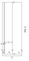
- FIG. 1shows a top view of a conventional substrate 10 , which is used to form a floating-body FET element 12 according to the prior art.
- the floating-body FET element 12includes an active region 14 , which is formed in the conventional substrate 10 .
- the active region 14includes a conventional source 16 , a floating body 18 , and a conventional drain 20 .
- the floating body 18is between the conventional source 16 and the conventional drain 20 and provides a channel for the floating-body FET element 12 .
- the conventional source 16 and the conventional drain 20include N-type semiconductor material, and the floating body 18 includes P-type semiconductor material.
- the conventional source 16 and the conventional drain 20include P-type semiconductor material, and the floating body 18 includes N-type semiconductor material.
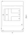
- FIG. 2shows a top view of details of the floating-body FET element 12 illustrated in FIG. 1 according to the prior art.
- the floating-body FET element 12includes a conventional gate 22 over the conventional substrate 10 .
- the conventional gate 22has a gate length 24 and a gate width 26 over the channel of the floating-body FET element 12 .
- the conventional gate 22may completely cover the floating body 18 as shown.
- the conventional gate 22may have a gate contact 28
- the conventional source 16may have source contacts 30
- the conventional drain 20may have drain contacts 32 .
- the gate, the source, and the drain contacts 28 , 30 , 32provide electrical connectivity to the conventional gate 22 , the conventional source 16 , and the conventional drain 20 , respectively.
- the floating body 18has no electrical contacts and is electrically coupled to other devices only through the conventional substrate 10 , the conventional gate 22 , the conventional source 16 , the conventional drain 20 , or any combination thereof.
- FIG. 3shows a cross-section of a thin-film semiconductor die 34 , which may be a thin-film silicon-on-insulator (SOI) semiconductor die, according to one embodiment of the thin-film semiconductor die 34 .
- the thin-film semiconductor die 34includes a substrate 36 , which may be an SOI substrate; an insulating layer 38 , which may be an SOI insulating layer, over the substrate 36 ; and a thin-film semiconductor device layer 40 , which may be a thin-film SOI device layer, over the insulating layer 38 .
- the thin-film semiconductor device layer 40has a semiconductor device layer thickness 42 and the insulating layer 38 has an insulating layer thickness 44 .
- the substrate 36may include silicon, sapphire, other semiconductor material, insulating material, or any combination thereof.
- the substrate 36may be provided from a silicon handle wafer.
- the insulating layer 38may include oxide, buried oxide, silicon dioxide, other insulating material, or any combination thereof.
- the thin-film semiconductor device layer 40is a thin-film layer that includes silicon and is used to form electronic devices, such as transistor elements, diode elements, resistive elements, capacitive elements, or the like.
- the insulating layer 38may be used to electrically isolate the thin-film semiconductor device layer 40 from the substrate 36 .
- the thin-film semiconductor device layer 40is partially-depleted SOI and not fully-depleted SOI.
- the insulating layer thickness 44increases, RF coupling to adjacent devices through the substrate 36 may be reduced, thereby improving isolation. Additionally, as resistivity of the substrate 36 increases, RF coupling to adjacent devices may be reduced, thereby improving RF performance of active RF devices and passive RF devices, such as inductors and transmission lines.
- the resistivity of the substrate 36is greater than about 100 ohm-centimeters. In a second exemplary embodiment of the substrate 36 , the resistivity of the substrate 36 is greater than about 500 ohm-centimeters. In a third exemplary embodiment of the substrate 36 , the resistivity of the substrate 36 is greater than about 1000 ohm-centimeters. In one embodiment of the thin-film semiconductor die 34 , the insulating layer thickness 44 is greater than the semiconductor device layer thickness 42 . In a first exemplary embodiment of the thin-film semiconductor device layer 40 , the semiconductor device layer thickness 42 is between about 100 nanometers and about 300 nanometers.
- the semiconductor device layer thickness 42is less than about 900 nanometers. In a third exemplary embodiment of the thin-film semiconductor device layer 40 , the semiconductor device layer thickness 42 is less than about 700 nanometers. In a fourth exemplary embodiment of the thin-film semiconductor device layer 40 , the semiconductor device layer thickness 42 is less than about 500 nanometers. In a fifth exemplary embodiment of the thin-film semiconductor device layer 40 , the semiconductor device layer thickness 42 is less than about 300 nanometers. In a sixth exemplary embodiment of the thin-film semiconductor device layer 40 , the semiconductor device layer thickness 42 is less than about 200 nanometers. In a seventh exemplary embodiment of the thin-film semiconductor device layer 40 , the semiconductor device layer thickness 42 is less than about 100 nanometers.
- the insulating layer thickness 44is between about 200 nanometers and about 1000 nanometers. In a second exemplary embodiment of the insulating layer 38 , the insulating layer thickness 44 is greater than about 200 nanometers. In a third exemplary embodiment of the insulating layer 38 , the insulating layer thickness 44 is greater than about 600 nanometers. In a fourth exemplary embodiment of the insulating layer 38 , the insulating layer thickness 44 is greater than about 1000 nanometers. In a fifth exemplary embodiment of the insulating layer 38 , the insulating layer thickness 44 is greater than about 1500 nanometers. In a sixth exemplary embodiment of the insulating layer 38 , the insulating layer thickness 44 is greater than about 2000 nanometers.
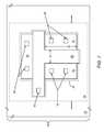
- FIG. 4shows a top view of a first body-contacted FET element 46 formed using the thin-film semiconductor die 34 illustrated in FIG. 3 according to one embodiment of the first body-contacted FET element 46 .
- the first body-contacted FET element 46includes an active region 48 , which is formed in the thin-film semiconductor device layer 40 .
- the active region 48includes a first source 50 , a first body 52 , and a first drain 54 .
- the first body 52is between the first source 50 and the first drain 54 and provides a channel for the first body-contacted FET element 46 .
- Either or both of the first source 50 and the first drain 54may include heavily doped semiconductor material to increase connectivity and provide one or more regions for making electrical connections to the first source 50 and the first drain 54 , respectively.
- the first source 50 and the first drain 54include N-type semiconductor material, and the first body 52 includes P-type semiconductor material.
- the first source 50 and the first drain 54include heavily doped N-type semiconductor material, and the first body 52 includes P-type semiconductor material.
- the first source 50 and the first drain 54include P-type semiconductor material, and the first body 52 includes N-type semiconductor material.
- the first source 50 and the first drain 54include heavily doped P-type semiconductor material, and the first body 52 includes N-type semiconductor material.
- FIG. 5shows a top view of details of the first body-contacted FET element 46 illustrated in FIG. 4 according to an alternate embodiment of the first body-contacted FET element 46 .
- the first body 52 of the first body-contacted FET element 46includes a first body contact region 56 , which may include heavily doped semiconductor material to increase connectivity and provide one or more regions for making electrical connections to the first body 52 .
- the first body 52includes P-type semiconductor material and the first body contact region 56 includes heavily doped P-type semiconductor material.
- the first body 52includes N-type semiconductor material and the first body contact region 56 includes heavily doped N-type semiconductor material.
- FIG. 6shows a top view of details of the first body-contacted FET element 46 illustrated in FIG. 5 according to an additional embodiment of the first body-contacted FET element 46 .
- the first body-contacted FET element 46includes insulating material 58 in the thin-film semiconductor device layer 40 and may completely surround the active region 48 . Completely surrounding the active region 48 with the insulating material 58 may substantially eliminate conduction paths between the first body-contacted FET element 46 and other devices through the thin-film semiconductor device layer 40 .
- all regions outside of the active region 48may be fully oxide isolated as part of the normal CMOS process.
- a CMOS shallow trenchmay be everywhere outside of active regions 48 and may extend down to the insulating layer 38 ( FIG. 3 ).
- FIG. 7shows a top view of details of the first body-contacted FET element 46 illustrated in FIG. 4 according to another embodiment of the first body-contacted FET element 46 .
- the first body-contacted FET element 46includes a first gate 60 over the thin-film semiconductor device layer 40 .
- the first gate 60has the gate length 24 and the gate width 26 over the channel of the first body-contacted FET element 46 .
- the first gate 60may have a first gate contact 62
- the first source 50may have first source contacts 64
- the first drain 54may have first drain contacts 66
- the first body contact region 56may have first body contacts 68 .
- the first gate, the first source, the first drain, and the first body contacts 62 , 64 , 66 , 68may provide electrical connectivity to the first gate 60 , the first source 50 , the first drain 54 , and the first body 52 , respectively.
- the first gate 60may extend over the insulating material 58 , beyond the insulating material 58 , or both.
- the first gate 60includes polysilicon.
- FIG. 8shows a cross-section of the thin-film semiconductor die 34 illustrated in FIG. 3 according to an alternate embodiment of the thin-film semiconductor die 34 .
- FIG. 8shows a cross-section of the first body-contacted FET element 46 , a second body-contacted FET element 70 , and a third body-contacted FET element 72 formed using the thin-film semiconductor device layer 40 .
- the first body-contacted FET element 46includes the first source 50 , the first body 52 , the first drain 54 , the insulating material 58 , a gate oxide 74 over the first body 52 , and the first gate 60 over the gate oxide 74 .
- the first body 52is between the first source 50 and the first drain 54 , and the first source 50 , the first body 52 , and the first drain 54 are surrounded by the insulating material 58 .
- the gate oxide 74electrically insulates the first gate 60 from the first body 52 .
- the first source 50 , the first body 52 , the first drain 54 , or any combination thereofmay completely traverse the semiconductor device layer thickness 42 ( FIG. 3 ) of the thin-film semiconductor device layer 40 .
- the first source 50 and the first drain 54include N-type silicon
- the first body 52includes P-type silicon.
- the first source 50 and the first drain 54include P-type silicon, and the first body 52 includes N-type silicon.
- Alternate embodiments of the first body-contacted FET element 46 , the second body-contacted FET element 70 , the third body-contacted FET element 72 , the like, or any combination thereofmay be formed using alternate layers, additional layers, or both having any type of implant or doping.
- the second body-contacted FET element 70may be similar to the first body-contacted FET element 46 and may include a second source 76 , a second body 78 , a second drain 80 , the insulating material 58 , the gate oxide 74 over the second body 78 , and a second gate 82 over the gate oxide 74 .
- the second body 78is between the second source 76 and the second drain 80 , and the second source 76 , the second body 78 , and the second drain 80 are surrounded by the insulating material 58 .
- the gate oxide 74electrically insulates the second gate 82 from the second body 78 .
- the second body-contacted FET element 70may include a second body contact region (not shown) and second body contacts (not shown).
- the second source 76 , the second body 78 , the second drain 80 , or any combination thereofmay completely traverse the semiconductor device layer thickness 42 ( FIG. 3 ) of the thin-film semiconductor device layer 40 .
- the second source 76 and the second drain 80include N-type silicon, and the second body 78 includes P-type silicon.
- the second source 76 and the second drain 80include P-type silicon, and the second body 78 includes N-type silicon.
- the third body-contacted FET element 72may be similar to the first body-contacted FET element 46 and may include a third source 84 , a third body 86 , a third drain 88 , the insulating material 58 , the gate oxide 74 over the third body 86 , and a third gate 90 over the gate oxide 74 .
- the third body 86is between the third source 84 and the third drain 88 , and the third source 84 , the third body 86 , and the third drain 88 are surrounded by the insulating material 58 .
- the gate oxide 74electrically insulates the third gate 90 from the third body 86 .
- the third body-contacted FET element 72may include a third body contact region (not shown) and third body contacts (not shown).
- the third source 84 , the third body 86 , the third drain 88 , or any combination thereofmay completely traverse the semiconductor device layer thickness 42 ( FIG. 3 ) of the thin-film semiconductor device layer 40 .
- the third source 84 and the third drain 88include N-type silicon, and the third body 86 includes P-type silicon.
- the third source 84 and the third drain 88include P-type silicon, and the third body 86 includes N-type silicon.
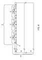
- a first body-contacted RF switch 92includes the first body-contacted FET element 46 , the second body-contacted FET element 70 , and the third body-contacted FET element 72 according to one embodiment of the first body-contacted RF switch 92 .
- the insulating material 58extends completely though the thin-film semiconductor device layer 40 down to the insulating layer 38 , such that the insulating material 58 completely surrounds each of the first body-contacted FET element 46 , the second body-contacted FET element 70 , and the third body-contacted FET element 72 , thereby substantially eliminating conduction paths between the first, the second, and the third body-contacted FET elements 46 , 70 , 72 through the substrate 36 , through the thin-film semiconductor device layer 40 , or both.
- FIG. 9shows a cross-section of the thin-film semiconductor die 34 according to an additional embodiment of the thin-film semiconductor die 34 .
- the thin-film semiconductor die 34 illustrated in FIG. 9is similar to the thin-film semiconductor die 34 illustrated in FIG. 8 , except that the thin-film semiconductor die 34 illustrated in FIG. 9 further includes the first source contact 64 , the first drain contact 66 , a second source contact 94 , a second drain contact 96 , a third source contact 98 , a third drain contact 100 , a first switch connection node 102 , a second switch connection node 104 , a first FET interconnect 106 , and a second FET interconnect 108 .
- the contacts 64 , 66 , 94 , 96 , 98 , 100may be vias that traverse one or more layers of the thin-film semiconductor die 34 . Any or all of the first switch connection node 102 , the second switch connection node 104 , the first FET interconnect 106 , and the second FET interconnect 108 may be provided by one or more metallization layers of the thin-film semiconductor die 34 .
- the first source contact 64is electrically connected to the first source 50 ; the first drain contact 66 is electrically connected to the first drain 54 ; the second source contact 94 is electrically connected to the second source 76 ; the second drain contact 96 is electrically connected to the second drain 80 ; the third source contact 98 is electrically connected to the third source 84 ; and the third drain contact 100 is electrically connected to the third drain 88 .
- the first switch connection node 102 of the first body-contacted RF switch 92is electrically connected to the third source 84 through the third source contact 98 .
- the second switch connection node 104 of the first body-contacted RF switch 92is electrically connected to the first drain 54 through the first drain contact 66 .
- the first FET interconnect 106electrically connects the first source 50 to the second drain 80 through the first source contact 64 and the second drain contact 96 , respectively.
- the second FET interconnect 108electrically connects the second source 76 to the third drain 88 through the second source contact 94 and the third drain contact 100 , respectively.
- the first body-contacted FET element 46 , the second body-contacted FET element 70 , and the third body-contacted FET element 72are coupled in series between the first switch connection node 102 and the second switch connection node 104 .
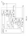
- FIG. 10is a schematic diagram showing the first body-contacted RF switch 92 illustrated in FIG. 9 according to one embodiment of the first body-contacted RF switch 92 .
- the first body-contacted RF switch 92includes the first body-contacted FET element 46 , the second body-contacted FET element 70 , the third body-contacted FET element 72 , the first switch connection node 102 , the second switch connection node 104 , a first body bias input FBBI, a first switch control input FSCI, and a resistor bias network 110 .
- the first switch control input FSCImay receive a first switch control signal 112 and the first body bias input FBBI may receive a first body bias control signal 114 .
- the first body-contacted FET element 46 , the second body-contacted FET element 70 , and the third body-contacted FET element 72are coupled in series between the first switch connection node 102 and the second switch connection node 104 , such that the third source 84 is coupled to the first switch connection node 102 , the third drain 88 is coupled to the second source 76 , the second drain 80 is coupled to the first source 50 , and the first drain 54 is coupled to the second switch connection node 104 .
- the resistor bias network 110is coupled to the first source 50 , the first body 52 , the first drain 54 , the first gate 60 , the second source 76 , the second body 78 , the second drain 80 , the second gate 82 , the third source 84 , the third body 86 , the third drain 88 , the third gate 90 , the first body bias input FBBI, and the first switch control input FSCI.
- the resistor bias network 110may provide appropriate bias behavior to the first source 50 , the first body 52 , the first drain 54 , the first gate 60 , the second source 76 , the second body 78 , the second drain 80 , the second gate 82 , the third source 84 , the third body 86 , the third drain 88 , and the third gate 90 based on the first switch control signal 112 , the first body bias control signal 114 , signals between the first switch connection node 102 and the second switch connection node 104 , or any combination thereof.
- FIG. 11is a schematic diagram showing details of the resistor bias network 110 illustrated in FIG. 10 according to one embodiment of the resistor bias network 110 .
- the resistor bias network 110includes a first body bias resistive element RB 1 , a second body bias resistive element RB 2 , a third body bias resistive element RB 3 , a common body bias resistive element RBC, a first gate resistive element RG 1 , a second gate resistive element RG 2 , a third gate resistive element RG 3 , a common gate resistive element RGC, a first drain-to-source resistive element RDS 1 , a second drain-to-source resistive element RDS 2 , and a third drain-to-source resistive element RDS 3 .
- the first gate resistive element RG 1is coupled between the first gate 60 and a gate node (not shown) to provide a first gate signal 115 to the first gate 60 .
- the second gate resistive element RG 2is coupled between the second gate 82 and the gate node to provide a second gate signal 116 to the second gate 82 .
- the third gate resistive element RG 3is coupled between the third gate 90 and the gate node to provide a third gate signal 118 to the third gate 90 .
- the common gate resistive element RGCis coupled between the gate node and the first switch control input FSCI.
- the first switch control input FSCImay receive the first switch control signal 112 , such that the first, the second, and the third gate signals 115 , 116 , 118 are based on the first switch control signal 112 .
- the first switch control signal 112is used to select either the ON state or the OFF state of the first body-contacted RF switch 92 . Selection between the ON state and the OFF state normally occurs at a much lower frequency than the frequency of RF signals between the first and the second switch connection nodes 102 , 104 . As such, the first switch control signal 112 may have direct current (DC)-like influences on the first body-contacted RF switch 92 .
- DCdirect current
- the first, the second, and the third gate resistive elements RG 1 , RG 2 , RG 3may have large values of resistance to isolate the first, the second, and the third gates 60 , 82 , 90 from one another.
- the first body-contacted RF switch 92will have one of the ON state, the OFF state, or a non-operating state.
- the first body bias resistive element RB 1is coupled between the first body 52 and a body bias node (not shown) to provide a first body bias signal 120 to the first body 52 .
- the second body bias resistive element RB 2is coupled between the second body 78 and the body bias node to provide a second body bias signal 122 to the second body 78 .
- the third body bias resistive element RB 3is coupled between the third body 86 and the body bias node to provide a third body bias signal 124 to the third body 86 .
- the common body bias resistive element RBCis coupled between the body bias node and the first body bias input FBBI.
- the first body bias input FBBImay receive the first body bias control signal 114 , such that the first, the second, and the third body bias signals 120 , 122 , 124 are based on the first body bias control signal 114 .
- the first body bias control signal 114may be used to provide an appropriate body bias to the first, the second, and the third bodies 52 , 78 , 86 , depending on whether the ON state or the OFF state of the first body-contacted RF switch 92 is selected. As mentioned above, selection between the ON state and the OFF state normally occurs at a much lower frequency than the frequency of RF signals between the first and the second switch connection nodes 102 , 104 .
- the frequency of the first body bias control signal 114normally occurs at a much lower frequency than the frequency of RF signals between the first and the second switch connection nodes 102 , 104 .
- the first body bias control signal 114may have DC like influences on the first body-contacted RF switch 92 .
- the first, the second, and the third body bias resistive elements RB 1 , RB 2 , RB 3may have large values of resistance to isolate the first, the second, and the third bodies 52 , 78 , 86 from one another.
- the first drain-to-source resistive element RDS 1is coupled between the first drain 54 and the first source 50
- the second drain-to-source resistive element RDS 2is coupled between the second drain 80 and the second source 76
- the third drain-to-source resistive element RDS 3is coupled between the third drain 88 and the third source 84 .
- the first, the second, and the third drain-to-source resistive elements RDS 1 , RDS 2 , RDS 3may provide about equal voltage division across the first, the second, and the third body-contacted FET elements 46 , 70 , 72 .
- a magnitude of the first body bias control signal 114is about equal to a magnitude of the first switch control signal 112 , and during the ON state of the first body-contacted RF switch 92 , the magnitude of the first body bias control signal 114 is not equal to the magnitude of the first switch control signal 112 .
- the magnitude of the first body bias control signal 114is about equal to the magnitude of the first switch control signal 112 , the magnitude of the first switch control signal 112 is negative relative to a DC voltage at the first switch connection node 102 , and the magnitude of the first switch control signal 112 is negative relative to a DC voltage at the second switch connection node 104 .
- the magnitude of the first switch control signal 112is positive relative to the magnitude of the first body bias control signal 114 .
- the magnitude of the first body bias control signal 114is about equal to the magnitude of the first switch control signal 112 , the magnitude of the first switch control signal 112 is positive relative to the DC voltage at the first switch connection node 102 , and the magnitude of the first switch control signal 112 is positive relative to the DC voltage at the second switch connection node 104 .
- the magnitude of the first switch control signal 112is negative relative to the magnitude of the first body bias control signal 114 .
- the first body bias control signal 114is equal to between about ⁇ 1 volt DC (VDC) and about ⁇ 5VDC
- the first switch control signal 112is equal to between about ⁇ 1VDC and about ⁇ 5VDC
- the DC voltage at the first switch connection node 102is equal to about zero volts
- the DC voltage at the second switch connection node 104is equal to about zero volts.
- the first body bias control signal 114is equal to about zero VDC
- the first switch control signal 112is equal to between about 1VDC and about 5VDC
- the DC voltage at the first switch connection node 102is equal to about zero volts
- the DC voltage at the second switch connection node 104is equal to about zero volts.
- the first body-contacted RF switch 92has an OFF state impedance between the first and the second switch connection nodes 102 , 104 .
- the first body-contacted RF switch 92has an ON state impedance between the first and the second switch connection nodes 102 , 104 .
- the first, the second, and the third body-contacted FET elements 46 , 70 , 72are coupled in series between the first and the second switch connection nodes 102 , 104 . As such, three body-contacted FET elements are coupled in series.
- the second body-contacted FET element 70is omitted, such that the third drain 88 is directly coupled to the first source 50 .
- two body-contacted FET elementsare coupled in series.
- any number of body-contacted FET elementsmay be coupled in series.
- FIG. 12is a schematic diagram showing the first body-contacted RF switch 92 according to an alternate embodiment of the first body-contacted RF switch 92 .
- the first body-contacted RF switch 92 illustrated in FIG. 12is similar to the first body-contacted RF switch 92 illustrated in FIG. 10 , except the first body-contacted RF switch 92 illustrated in FIG. 12 may include any number of body-contacted FET elements.
- the first body-contacted RF switch 92includes the first body-contacted FET element 46 , the second body-contacted FET element 70 , and up to and including an N TH body-contacted FET element 126 .
- the N TH body-contacted FET element 126includes an N TH source 128 , an N TH body 130 , an N TH drain 132 , and an N TH gate 134 .
- the N TH body-contacted FET element 126 and any intervening body-contacted FET elements (not shown) between the second body-contacted FET element 70 and the N TH body-contacted FET element 126may be similar to the first body-contacted FET element 46 as previously described.
- the first body-contacted FET element 46 , the second body-contacted FET element 70 , and up to and including the N TH body-contacted FET element 126are coupled in series between the first switch connection node 102 and the second switch connection node 104 , such that the N TH source 128 is coupled to the first switch connection node 102 , the N TH drain 132 is coupled to the second source 76 through any intervening body-contacted FET elements (not shown), the second drain 80 is coupled to the first source 50 , and the first drain 54 is coupled to the second switch connection node 104 .
- the resistor bias network 110provides the first gate signal 115 to the first gate 60 , the second gate signal 116 to the second gate 82 , and an N TH gate signal 136 to the N TH gate 134 .
- the first switch control input FSCImay receive the first switch control signal 112 , such that the first, the second, and up to and including the N TH gate signals 115 , 116 , 136 are based on the first switch control signal 112 .
- the first switch control signal 112is used to select either the ON state or the OFF state of the first body-contacted RF switch 92 .
- the resistive bias network 110provides the first body bias signal 120 to the first body 52 , the second body bias signal 122 to the second body 78 , and an N TH body bias signal 138 to the N TH body 130 .
- the first body bias input FBBImay receive the first body bias control signal 114 , such that the first, the second, and up to and including the N TH body bias signals 120 , 122 , 138 are based on the first body bias control signal 114 .
- the first body bias control signal 114may be used to provide an appropriate body bias to the first, the second, and up to and including the N TH bodies 52 , 78 , 130 , depending on whether the ON state or the OFF state of the first body-contacted RF switch 92 is selected.
- the first body-contacted RF switch 92includes a quantity of series coupled body-contacted FET elements equal to N, such that N is any positive whole number greater than one.
- An RF signal 140 between the first and the second switch connection nodes 102 , 104may be present due to the first body-contacted RF switch 92 interacting with other circuit elements (not shown).
- a frequency of the RF signal 140is greater than about 100 megahertz.
- the RF signal 140may be distributed across the first body-contacted FET element 46 , the second body-contacted FET element 70 , and up to and including the N TH body-contacted FET element 126 .
- the RF signal 140is distributed about equally across the first body-contacted FET element 46 , the second body-contacted FET element 70 , and up to and including the N TH body-contacted FET element 126 .
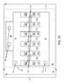
- FIG. 13shows an RF switch system 142 according to one embodiment of the RF switch system 142 .
- the RF switch system 142provides four switched ports and includes the first body-contacted RF switch 92 , a second body-contacted RF switch 144 , a third body-contacted RF switch 146 , a fourth body-contacted RF switch 148 , and control circuitry 150 .
- the second, the third, and the fourth body-contacted RF switches 144 , 146 , 148may be similar to the first body-contacted RF switch 92 .
- the second body-contacted RF switch 144has a third switch connection node 152 and a fourth switch connection node 154 , which may be similar to the first switch connection node 102 and the second switch connection node 104 , respectively. Further, the second body-contacted RF switch 144 has a second body bias input SBBI and a second switch control input SSCI, which may be similar to the first body bias input FBBI and the first switch control input FSCI, respectively.
- the third body-contacted RF switch 146has a fifth switch connection node 156 and a sixth switch connection node 158 , which may be similar to the first switch connection node 102 and the second switch connection node 104 , respectively. Further, the third body-contacted RF switch 146 has a third body bias input TBBI and a third switch control input TSCI, which may be similar to the first body bias input FBBI and the first switch control input FSCI, respectively.
- the fourth body-contacted RF switch 148has a seventh switch connection node 160 and an eighth switch connection node 162 , which may be similar to the first switch connection node 102 and the second switch connection node 104 , respectively. Further, the fourth body-contacted RF switch 148 has a fourth body bias input FOBBI and a fourth switch control input FOSCI, which may be similar to the first body bias input FBBI and the first switch control input FSCI, respectively.
- Each of the first, the second, the third, and the fourth body-contacted RF switches 92 , 144 , 146 , 148provides a switched port of the RF switch system 142 .
- the second, the fourth, the sixth, and the eighth switch connection nodes 104 , 154 , 158 , 162are coupled to an RF antenna 164 .
- the first, the third, the fifth, and the seventh switch connection nodes 102 , 152 , 156 , 160provide a first port 166 , a second port 168 , a third port 170 , and a fourth port 172 , respectively.
- the first, the second, the third, and the fourth body-contacted RF switches 92 , 144 , 146 , 148allow the first, the second, the third, and the fourth ports 166 , 168 , 170 , 172 to share the RF antenna 164 .
- Any or all of the first, the second, the third, and the fourth ports 166 , 168 , 170 , 172may be coupled to RF transmit circuitry (not shown), RF receive circuitry (not shown), RF diplexers (not shown), RF duplexers (not shown), the like (not shown), or any combination thereof (not shown).
- the control circuitry 150provides the first switch control signal 112 , a second switch control signal 174 , a third switch control signal 176 , and a fourth switch control signal 178 to the first switch control input FSCI, the second switch control input SSCI, the third switch control input TSCI, and the fourth switch control input FOSCI, respectively.
- the control circuitry 150selects either the OFF state of the first body-contacted RF switch 92 or the ON state of the first body-contacted RF switch 92 and provides the first switch control signal 112 based on the selected one of the OFF state and the ON state to indicate which state was selected.
- the control circuitry 150selects either an OFF state of the second body-contacted RF switch 144 or an ON state of the second body-contacted RF switch 144 and provides the second switch control signal 174 based on the selected one of the OFF state and the ON state to indicate which state was selected.
- the control circuitry 150selects either an OFF state of the third body-contacted RF switch 146 or an ON state of the third body-contacted RF switch 146 and provides the third switch control signal 176 based on the selected one of the OFF state and the ON state to indicate which state was selected.
- the control circuitry 150selects either an OFF state of the fourth body-contacted RF switch 148 or an ON state of the fourth body-contacted RF switch 148 and provides the fourth switch control signal 178 based on the selected one of the OFF state and the ON state to indicate which state was selected.
- the control circuitry 150provides the first body bias control signal 114 , a second body bias control signal 180 , a third body bias control signal 182 , and a fourth body bias control signal 184 to the first body bias input FBBI, the second body bias input SBBI, the third body bias input TBBI, and the fourth body bias input FOBBI, respectively.
- the control circuitry 150provides the first body bias control signal 114 based on the selected one of the OFF state and the ON state of the first body-contacted RF switch 92 to provide the appropriate body biasing to the body-contacted FET elements (not shown) in the first body-contacted RF switch 92 .
- the control circuitry 150provides the second body bias control signal 180 based on the selected one of the OFF state and the ON state of the second body-contacted RF switch 144 to provide the appropriate body biasing to the body-contacted FET elements (not shown) in the second body-contacted RF switch 144 .
- the control circuitry 150provides the third body bias control signal 182 based on the selected one of the OFF state and the ON state of the third body-contacted RF switch 146 to provide the appropriate body biasing to the body-contacted FET elements (not shown) in the third body-contacted RF switch 146 .
- the control circuitry 150provides the fourth body bias control signal 184 based on the selected one of the OFF state and the ON state of the fourth body-contacted RF switch 148 to provide the appropriate body biasing to the body-contacted FET elements (not shown) in the fourth body-contacted RF switch 148 .
- RF switch system 142may omit any or all of the second, the third, and the fourth body-contacted RF switches 144 , 146 , 148 , or may include additional body-contacted RF switches (not shown). Further, the body-contacted RF switches may be arranged in any manner.
- FIG. 14shows the RF switch system 142 according to an alternate embodiment of the RF switch system 142 .
- the RF switch system 142 illustrated in FIG. 14is similar to the RF switch system 142 illustrated in FIG. 13 except the RF switch system 142 illustrated in FIG. 14 uses the second, the third, and the fourth body-contacted RF switches 144 , 146 , 148 in a different manner.
- the second, the fourth, the sixth, and the eighth switch connection nodes 104 , 154 , 158 , 162are coupled to the RF antenna 164 .
- the first, the third, the fifth, and the seventh switch connection nodes 102 , 152 , 156 , 160provide the first, the second, the third, and the fourth ports 166 , 168 , 170 , 172 , respectively. In FIG. 14 , the third and the fourth ports 170 , 172 are omitted.
- the first and the third switch connection nodes 102 , 152provide the first port 166
- the fifth and the seventh switch connection nodes 156 , 160provide the second port 168 .
- the second and the sixth switch connection nodes 104 , 158are coupled to the RF antenna 164
- the fourth and the eighth switch connection nodes 154 , 162are coupled to ground. As such, the second and the fourth body-contacted RF switches 144 , 148 function as shunt switches.
- the second body-contacted RF switch 144is in the ON state and vice versa.
- the first switch connection node 102to ground when the first body-contacted RF switch 92 is in the OFF state and the second body-contacted RF switch 144 is in the ON state may improve isolation characteristics of the first body-contacted RF switch 92 .
- the fourth body-contacted RF switch 148is in the ON state and vice versa.
- the RF switch system 142may omit any or all of the second, the third, and the fourth body-contacted RF switches 144 , 146 , 148 , or may include additional body-contacted RF switches (not shown). Further, the body-contacted RF switches may be arranged in any manner.
- the mobile terminal 186may include a receiver front end 188 , a radio frequency transmitter section 190 , an antenna 192 , the RF switch system 142 , a baseband processor 194 , a control system 196 , a frequency synthesizer 198 , and an interface 200 .
- the receiver front end 188receives information bearing radio frequency signals from one or more remote transmitters provided by a base station (not shown).
- a low noise amplifier (LNA) 202amplifies the signal.
- LNAlow noise amplifier
- a filter circuit 204minimizes broadband interference in the received signal, while down conversion and digitization circuitry 206 down converts the filtered, received signal to an intermediate or baseband frequency signal, which is then digitized into one or more digital streams.
- the receiver front end 188typically uses one or more mixing frequencies generated by the frequency synthesizer 198 .
- the baseband processor 194processes the digitized received signal to extract the information or data bits conveyed in the received signal. This processing typically comprises demodulation, decoding, and error correction operations. As such, the baseband processor 194 is generally implemented in one or more digital signal processors (DSPs).
- DSPsdigital signal processors
- the baseband processor 194receives digitized data, which may represent voice, data, or control information, from the control system 196 , which it encodes for transmission.
- the encoded datais output to the transmitter 190 , where it is used by a modulator 208 to modulate a carrier signal that is at a desired transmit frequency.
- Power amplifier circuitry 210amplifies the modulated carrier signal to a level appropriate for transmission, and delivers the amplified and modulated carrier signal to the antenna 192 through the RF switch system 142 .
- a usermay interact with the mobile terminal 186 via the interface 200 , which may include interface circuitry 212 associated with a microphone 214 , a speaker 216 , a keypad 218 , and a display 220 .
- the interface circuitry 212typically includes analog-to-digital converters, digital-to-analog converters, amplifiers, and the like. Additionally, it may include a voice encoder/decoder, in which case it may communicate directly with the baseband processor 194 .
- the microphone 214will typically convert audio input, such as the user's voice, into an electrical signal, which is then digitized and passed directly or indirectly to the baseband processor 194 .
- Audio information encoded in the received signalis recovered by the baseband processor 194 , and converted by the interface circuitry 212 into an analog signal suitable for driving the speaker 216 .
- the keypad 218 and display 220enable the user to interact with the mobile terminal 186 , input numbers to be dialed, address book information, or the like, as well as monitor call progress information.
- FIG. 16is a graph illustrating a relationship between a body-contacted RF switch OFF capacitance of the first body-contacted RF switch 92 ( FIGS. 13 and 14 ) and an absolute value of reverse body biasing of the first body-contacted RF switch 92 .
- the body-contacted RF switch OFF capacitanceis between the first and the second switch connection nodes 102 , 104 ( FIGS. 13 and 14 ) when the first body-contacted RF switch 92 is in an OFF state.
- reverse body biasing each FET element, which is in an OFF state, in the first body-contacted RF switch 92may reduce drain-to-source capacitance of each FET element.
- the body-contacted RF switch OFF capacitancemay be reduced by the reverse body biasing.
- FIG. 16shows that as the absolute value of the reverse body biasing increases, the body-contacted RF switch OFF capacitance decreases, which may effectively increase RF isolation of the first body-contacted RF switch 92 .
- the insertion loss of the first body-contacted RF switch 92may be similar to the insertion loss of a similarly constructed floating-body RF switch. Therefore, reverse body biasing may improve the trade-off between insertion loss and RF isolation.
- reverse body biasingmay improve the linearity of the first body-contacted RF switch 92 by operating where the slope of the capacitance versus the reverse body biasing curve illustrated in FIG. 16 is shallow instead of steep.
- Linearity of an RF switchis provided by maintaining a constant RF switch OFF capacitance over changes in magnitudes of RF signal levels across the RF switch.
- RF signals across an RF switchmodulate the body biasing of the RF switch.
- modulating body biasingmodulates the RF switch OFF capacitance as illustrated in FIG. 16 .
- magnitudes of the RF signalsincrease, magnitudes of the modulations increase, thereby causing non-linearity in the RF switch 92 .
- FIG. 17is a graph illustrating a relationship between second harmonic power of both floating-body and body-contacted RF switches in an OFF state and input power to the RF switches.
- FIG. 18is a graph illustrating a relationship between third harmonic power of both floating-body and body-contacted RF switches in an OFF state and input power to the RF switches.
- Harmonic powermay be one measure of harmonic distortion, which may degrade the linearity of the first body-contacted RF switch 92 ( FIGS. 13 and 14 ). Harmonic distortion may be caused by changes in the body-contacted RF switch OFF capacitance resulting from the time-varying nature of RF signals between the first and the second switch connection nodes 102 , 104 of the first body-contacted RF switch 92 .
- the body-contacted RF switch OFF capacitancemay result from capacitances of series-coupled FET elements in the first body-contacted RF switch 92 .
- Each FET elementmay have a drain-to-body capacitance, a drain-to-gate capacitance, and a drain-to-source capacitance.
- the drain-to-body capacitancemay be reduced and may have a reduced sensitivity to changes in input power, when compared to a floating-body RF switch.
- the second harmonic power of the first body-contacted RF switch 92is slightly less than corresponding second harmonic power of the floating-body RF switch.
- the third harmonic power of the first body-contacted RF switch 92is significantly less than the third harmonic power of the floating-body RF switch, particularly as input power increases.
- FIG. 19shows a top view of details of the first body-contacted FET element 46 illustrated in FIG. 4 according to one embodiment of the first body-contacted FET element 46 .
- the first body-contacted FET element 46 illustrated in FIG. 19is similar to the first body-contacted FET element 46 illustrated in FIG. 7 , except in the first body-contacted FET element 46 illustrated in FIG. 19 , the first gate 60 has multiple gate fingers 222 , the first source 50 has multiple source fingers 224 , and the first drain 54 has multiple drain fingers 226 .
- Each of the multiple gate fingers 222may be between one of the multiple source fingers 224 and one of the multiple drain fingers 226 . Further, each of the multiple source fingers 224 may have at least one of the first source contacts 64 .
- each of the multiple drain fingers 226may have at least one of the first drain contacts 66 .
- Other embodiments of the first body-contacted FET element 46may have any arrangement of the first gate 60 , the first drain 54 , and the first source 50 including any number of source fingers 224 , drain fingers 226 , and gate fingers 222 .
- FIG. 20shows a top view of details of the first body-contacted FET element 46 illustrated in FIG. 4 according to an alternate embodiment of the first body-contacted FET element 46 .
- the first body-contacted FET element 46 illustrated in FIG. 20is similar to the first body-contacted FET element 46 illustrated in FIG. 19 , except in the first body-contacted FET element 46 illustrated in FIG. 20 , the multiple gate fingers 222 are coupled together at both ends instead of only at one end as illustrated in FIG. 19 . Further, both ends of the first gate 60 may have at least one first gate contact 62 .
- circuitrymay use discrete circuitry, integrated circuitry, programmable circuitry, non-volatile circuitry, volatile circuitry, software executing instructions on computing hardware, firmware executing instructions on computing hardware, the like, or any combination thereof.
- the computing hardwaremay include mainframes, micro-processors, micro-controllers, DSPs, the like, or any combination thereof.
Landscapes
- Engineering & Computer Science (AREA)
- Physics & Mathematics (AREA)
- Condensed Matter Physics & Semiconductors (AREA)
- General Physics & Mathematics (AREA)
- Manufacturing & Machinery (AREA)
- Computer Hardware Design (AREA)
- Microelectronics & Electronic Packaging (AREA)
- Power Engineering (AREA)
- Metal-Oxide And Bipolar Metal-Oxide Semiconductor Integrated Circuits (AREA)
Abstract
Description
Claims (25)
Priority Applications (2)
| Application Number | Priority Date | Filing Date | Title |
|---|---|---|---|
| US12/723,257US8723260B1 (en) | 2009-03-12 | 2010-03-12 | Semiconductor radio frequency switch with body contact |
| US14/276,370US20140242760A1 (en) | 2009-03-12 | 2014-05-13 | Semiconductor radio frequency switch with body contact |
Applications Claiming Priority (2)
| Application Number | Priority Date | Filing Date | Title |
|---|---|---|---|
| US15966809P | 2009-03-12 | 2009-03-12 | |
| US12/723,257US8723260B1 (en) | 2009-03-12 | 2010-03-12 | Semiconductor radio frequency switch with body contact |
Related Child Applications (1)
| Application Number | Title | Priority Date | Filing Date |
|---|---|---|---|
| US14/276,370DivisionUS20140242760A1 (en) | 2009-03-12 | 2014-05-13 | Semiconductor radio frequency switch with body contact |
Publications (1)
| Publication Number | Publication Date |
|---|---|
| US8723260B1true US8723260B1 (en) | 2014-05-13 |
Family
ID=50635616
Family Applications (2)
| Application Number | Title | Priority Date | Filing Date |
|---|---|---|---|
| US12/723,257Active2032-07-11US8723260B1 (en) | 2009-03-12 | 2010-03-12 | Semiconductor radio frequency switch with body contact |
| US14/276,370AbandonedUS20140242760A1 (en) | 2009-03-12 | 2014-05-13 | Semiconductor radio frequency switch with body contact |
Family Applications After (1)
| Application Number | Title | Priority Date | Filing Date |
|---|---|---|---|
| US14/276,370AbandonedUS20140242760A1 (en) | 2009-03-12 | 2014-05-13 | Semiconductor radio frequency switch with body contact |
Country Status (1)
| Country | Link |
|---|---|
| US (2) | US8723260B1 (en) |
Cited By (35)
| Publication number | Priority date | Publication date | Assignee | Title |
|---|---|---|---|---|
| US20130244595A1 (en)* | 2010-09-21 | 2013-09-19 | Dsp Group Ltd | Rf switch implementation in cmos process |
| US20130252562A1 (en)* | 2010-09-21 | 2013-09-26 | Dsp Group, Ltd. | High power high isolation low current cmos rf switch |
| US20130321095A1 (en)* | 2012-05-11 | 2013-12-05 | Skyworks Solutions, Inc. | Low-loss high-isolation switching architecture |
| US20140009211A1 (en)* | 2012-07-07 | 2014-01-09 | Skyworks Solutions, Inc. | Radio-frequency switch having gate node voltage compensation network |
| US20140227983A1 (en)* | 2013-02-11 | 2014-08-14 | Triquint Semiconductor, Inc. | Body-biased switching device |
| US8975950B2 (en) | 2012-07-07 | 2015-03-10 | Skyworks Solutions, Inc. | Switching device having a discharge circuit for improved intermodulation distortion performance |
| US9013225B2 (en) | 2013-02-04 | 2015-04-21 | Skyworks Solutions, Inc. | RF switches having increased voltage swing uniformity |
| US20150133065A1 (en)* | 2013-11-11 | 2015-05-14 | Samsung Electro-Mechanics Co., Ltd. | Rf switch |
| US9059702B2 (en) | 2012-07-07 | 2015-06-16 | Skyworks Solutions, Inc. | Switch linearization by non-linear compensation of a field-effect transistor |
| US20150214931A1 (en)* | 2014-01-28 | 2015-07-30 | Samsung Electro-Mechanics Co., Ltd. | Radio frequency switching circuit and electronic device |
| US9148194B2 (en) | 2012-07-07 | 2015-09-29 | Skyworks Solutions, Inc. | Radio-frequency switch system having improved intermodulation distortion performance |
| US9160328B2 (en) | 2012-07-07 | 2015-10-13 | Skyworks Solutions, Inc. | Circuits, devices, methods and applications related to silicon-on-insulator based radio-frequency switches |
| US9177968B1 (en) | 2014-09-19 | 2015-11-03 | Silanna Semiconductor U.S.A., Inc. | Schottky clamped radio frequency switch |
| US9197280B1 (en)* | 2014-05-09 | 2015-11-24 | Samsung Electro-Mechanics Co., Ltd. | Radio frequency switch |
| US9203396B1 (en) | 2013-02-22 | 2015-12-01 | Triquint Semiconductor, Inc. | Radio frequency switch device with source-follower |
| US20160027801A1 (en)* | 2014-02-19 | 2016-01-28 | Boe Technology Group Co., Ltd. | Array substrate, manufacturing method thereof and display panel |
| US20160126906A1 (en)* | 2014-11-03 | 2016-05-05 | Rf Micro Devices, Inc. | Low noise amplifier |
| US9379698B2 (en) | 2014-02-04 | 2016-06-28 | Triquint Semiconductor, Inc. | Field effect transistor switching circuit |
| CN106033961A (en)* | 2015-03-12 | 2016-10-19 | 瑞昱半导体股份有限公司 | Analog switch circuit |
| WO2016144762A3 (en)* | 2015-03-06 | 2016-10-20 | Qualcomm Incorporated | Rf circuit with switch transistor with body connection |
| US9628075B2 (en) | 2012-07-07 | 2017-04-18 | Skyworks Solutions, Inc. | Radio-frequency switch having dynamic body coupling |
| US20170201245A1 (en)* | 2016-01-08 | 2017-07-13 | Qorvo Us, Inc. | Rf branch with accelerated turn-on and high q value |
| US10147724B2 (en) | 2012-07-07 | 2018-12-04 | Skyworks Solutions, Inc. | Feed-forward circuit to improve intermodulation distortion performance of radio-frequency switch |
| US10270437B2 (en) | 2016-01-08 | 2019-04-23 | Qorvo Us, Inc. | RF switch having reduced signal distortion |
| US10320379B2 (en) | 2016-12-21 | 2019-06-11 | Qorvo Us, Inc. | Transistor-based radio frequency (RF) switch |
| US10326440B1 (en)* | 2018-02-28 | 2019-06-18 | Nxp Usa, Inc. | RF switches, integrated circuits, and devices with multi-gate field effect transistors and voltage leveling circuits, and methods of their fabrication |
| US10361697B2 (en)* | 2016-12-23 | 2019-07-23 | Skyworks Solutions, Inc. | Switch linearization by compensation of a field-effect transistor |
| US10608623B2 (en) | 2016-12-21 | 2020-03-31 | Qorvo US. Inc. | Transistor-based radio frequency (RF) switch |
| US10784862B1 (en) | 2019-09-10 | 2020-09-22 | Nxp Usa, Inc. | High speed switching radio frequency switches |
| US10972091B1 (en) | 2019-12-03 | 2021-04-06 | Nxp Usa, Inc. | Radio frequency switches with voltage equalization |
| TWI737600B (en)* | 2015-03-31 | 2021-09-01 | 美商西凱渥資訊處理科技公司 | Substrate bias for field-effect transistor devices |
| US11368180B2 (en) | 2020-07-31 | 2022-06-21 | Nxp Usa, Inc. | Switch circuits with parallel transistor stacks and methods of their operation |
| US20220368322A1 (en)* | 2021-05-12 | 2022-11-17 | Db Hitek Co., Ltd. | Rf switch device |
| US11683028B2 (en) | 2021-03-03 | 2023-06-20 | Nxp Usa, Inc. | Radio frequency switches with voltage equalization |
| US20230275127A1 (en)* | 2017-12-31 | 2023-08-31 | Skyworks Solutions, Inc. | Methods related to switch body connections to achieve soft breakdown |
Families Citing this family (6)
| Publication number | Priority date | Publication date | Assignee | Title |
|---|---|---|---|---|
| US9935092B2 (en)* | 2014-07-03 | 2018-04-03 | Ferfics Limited | Radio frequency transistor stack with improved linearity |
| US10847445B2 (en)* | 2016-03-31 | 2020-11-24 | Skyworks Solutions, Inc. | Non-symmetric body contacts for field-effect transistors |
| WO2018063397A1 (en)* | 2016-09-30 | 2018-04-05 | Intel Corporation | Gate trench precision resistors with high-k rmg gan transistor |
| CN110113036A (en)* | 2019-05-09 | 2019-08-09 | 河源广工大协同创新研究院 | A kind of radio-frequency switch circuit structure of High Linear low harmony wave |
| TWI747292B (en)* | 2019-07-12 | 2021-11-21 | 台灣積體電路製造股份有限公司 | Semiconductor device |
| CN115395936A (en)* | 2022-07-18 | 2022-11-25 | 上海唯捷创芯电子技术有限公司 | High-linearity radio frequency switch circuit, chip and electronic equipment thereof |
Citations (260)
| Publication number | Priority date | Publication date | Assignee | Title |
|---|---|---|---|---|
| US3699359A (en) | 1971-04-20 | 1972-10-17 | Philco Ford Corp | Electronic latching device |
| US3975671A (en) | 1975-02-24 | 1976-08-17 | Intel Corporation | Capacitive voltage converter employing CMOS switches |
| US3988727A (en) | 1974-06-24 | 1976-10-26 | P. R. Mallory & Co., Inc. | Timed switching circuit |
| US4244000A (en) | 1978-11-28 | 1981-01-06 | Nippon Telegraph And Telephone Public Corporation | PNPN Semiconductor switches |
| US4256977A (en) | 1978-12-26 | 1981-03-17 | Honeywell Inc. | Alternating polarity power supply control apparatus |
| US4316101A (en) | 1978-11-30 | 1982-02-16 | Licentia-Patent-Verwaltungs-G.M.B.H. | Circuit for switching and transmitting alternating voltages |
| US4317055A (en) | 1978-05-24 | 1982-02-23 | Hitachi, Ltd. | High-voltage circuit for insulated gate field-effect transistor |
| US4367421A (en) | 1980-04-21 | 1983-01-04 | Reliance Electric Company | Biasing methods and circuits for series connected transistor switches |
| US4456888A (en)* | 1981-03-26 | 1984-06-26 | Raytheon Company | Radio frequency network having plural electrically interconnected field effect transistor cells |
| US4748485A (en) | 1985-03-21 | 1988-05-31 | Hughes Aircraft Company | Opposed dual-gate hybrid structure for three-dimensional integrated circuits |
| US4809056A (en) | 1985-10-31 | 1989-02-28 | Fujitsu Limited | Semiconductor device having a silicon on insulator structure |
| US4810911A (en) | 1986-11-14 | 1989-03-07 | Nec Corp | FET switch circuit having small insertion loss and exhibiting stable operation |
| US4849651A (en) | 1988-02-24 | 1989-07-18 | Hughes Aircraft Company | Two-state, bilateral, single-pole, double-throw, half-bridge power-switching apparatus and power supply means for such electronic power switching apparatus |
| US4890077A (en) | 1989-03-28 | 1989-12-26 | Teledyne Mec | FET monolithic microwave integrated circuit variable attenuator |
| US4906587A (en) | 1988-07-29 | 1990-03-06 | Texas Instruments Incorporated | Making a silicon-on-insulator transistor with selectable body node to source node connection |
| US4929855A (en) | 1988-12-09 | 1990-05-29 | Grumman Corporation | High frequency switching device |
| US4984040A (en) | 1989-06-15 | 1991-01-08 | Xerox Corporation | High voltage thin film transistor with second gate |
| US4985647A (en) | 1988-06-21 | 1991-01-15 | Nec Corporation | CMOS transfer switch free from malfunction on noise signal |
| EP0385641A3 (en) | 1989-02-28 | 1991-02-27 | AT&T Corp. | A high efficiency uhf linear power amplifier |
| US5001528A (en) | 1989-01-31 | 1991-03-19 | The United States Of America As Represented By The Secretary Of The Air Force | Radiation hardened CMOS on SOI or SOS devices |
| US5012123A (en) | 1989-03-29 | 1991-04-30 | Hittite Microwave, Inc. | High-power rf switching system |
| US5061911A (en) | 1990-04-03 | 1991-10-29 | Motorola, Inc. | Single fault/tolerant MMIC switches |
| US5081706A (en) | 1987-07-30 | 1992-01-14 | Texas Instruments Incorporated | Broadband merged switch |
| US5095348A (en) | 1989-10-02 | 1992-03-10 | Texas Instruments Incorporated | Semiconductor on insulator transistor |
| US5124762A (en) | 1990-12-31 | 1992-06-23 | Honeywell Inc. | Gaas heterostructure metal-insulator-semiconductor integrated circuit technology |
| US5146178A (en) | 1990-11-16 | 1992-09-08 | Nippon Telegraph And Telephone Company | Impedance-matched, class F high-frequency amplifier |
| US5148393A (en) | 1988-07-07 | 1992-09-15 | Kabushiki Kaisha Toshiba | Mos dynamic semiconductor memory cell |
| US5157279A (en) | 1991-05-28 | 1992-10-20 | Samsung Electronics Co., Ltd. | Data output driver with substrate biasing producing high output gain |
| US5272457A (en) | 1992-03-10 | 1993-12-21 | Harris Corporation | High isolation integrated switch circuit |
| US5283457A (en) | 1989-10-02 | 1994-02-01 | Texas Instruments Incorporated | Semiconductor on insulator transistor |
| US5285367A (en) | 1992-02-07 | 1994-02-08 | Power Integrations, Inc. | Linear load circuit to control switching power supplies under minimum load conditions |
| US5306954A (en) | 1992-06-04 | 1994-04-26 | Sipex Corporation | Charge pump with symmetrical +V and -V outputs |
| US5313083A (en) | 1988-12-16 | 1994-05-17 | Raytheon Company | R.F. switching circuits |
| US5345422A (en) | 1990-07-31 | 1994-09-06 | Texas Instruments Incorporated | Power up detection circuit |
| US5350957A (en) | 1989-10-20 | 1994-09-27 | Texas Instrument Incorporated | Electronic switch controlled by plural inputs |
| EP0625831A2 (en) | 1993-05-21 | 1994-11-23 | Sony Corporation | Radio receiver-transmitter apparatus |
| US5375257A (en) | 1993-12-06 | 1994-12-20 | Raytheon Company | Microwave switch |
| US5405795A (en) | 1994-06-29 | 1995-04-11 | International Business Machines Corporation | Method of forming a SOI transistor having a self-aligned body contact |
| US5416043A (en) | 1993-07-12 | 1995-05-16 | Peregrine Semiconductor Corporation | Minimum charge FET fabricated on an ultrathin silicon on sapphire wafer |
| US5442327A (en) | 1994-06-21 | 1995-08-15 | Motorola, Inc. | MMIC tunable biphase modulator |
| US5448207A (en) | 1993-09-30 | 1995-09-05 | Sony Corporation | Attenuator circuit apparatus |
| US5477184A (en) | 1992-04-15 | 1995-12-19 | Sanyo Electric Co., Ltd. | Fet switching circuit for switching between a high power transmitting signal and a lower power receiving signal |
| US5488243A (en) | 1992-12-04 | 1996-01-30 | Nippondenso Co., Ltd. | SOI MOSFET with floating gate |
| US5493249A (en) | 1993-12-06 | 1996-02-20 | Micron Technology, Inc. | System powered with inter-coupled charge pumps |
| US5492857A (en) | 1993-07-12 | 1996-02-20 | Peregrine Semiconductor Corporation | High-frequency wireless communication system on a single ultrathin silicon on sapphire chip |
| US5528056A (en)* | 1990-11-30 | 1996-06-18 | Sharp Kabushiki Kaisha | CMOS thin-film transistor having split gate structure |
| US5553295A (en) | 1994-03-23 | 1996-09-03 | Intel Corporation | Method and apparatus for regulating the output voltage of negative charge pumps |
| US5559368A (en) | 1994-08-30 | 1996-09-24 | The Regents Of The University Of California | Dynamic threshold voltage mosfet having gate to body connection for ultra-low voltage operation |
| US5578853A (en) | 1992-12-10 | 1996-11-26 | Sony Corporation | Semiconductor memory cell having information storage transistor and switching transistor |
| US5594371A (en) | 1994-06-28 | 1997-01-14 | Nippon Telegraph And Telephone Corporation | Low voltage SOI (Silicon On Insulator) logic circuit |
| US5597739A (en) | 1994-01-19 | 1997-01-28 | Sony Corporation | MOS transistor and method for making the same |
| US5600588A (en) | 1994-01-24 | 1997-02-04 | Fujitsu Limited | Data retention circuit and semiconductor memory device using the same |
| US5610533A (en) | 1993-11-29 | 1997-03-11 | Mitsubishi Denki Kabushiki Kaisha | Switched substrate bias for logic circuits |
| US5616935A (en)* | 1994-02-08 | 1997-04-01 | Semiconductor Energy Laboratory Co., Ltd. | Semiconductor integrated circuit having N-channel and P-channel transistors |
| US5629655A (en) | 1992-10-27 | 1997-05-13 | Ericsson Inc. | Integrated distributed RC low-pass filters |
| EP0782267A2 (en) | 1995-12-27 | 1997-07-02 | Nec Corporation | Semiconductor switch |
| US5681761A (en) | 1995-12-28 | 1997-10-28 | Philips Electronics North America Corporation | Microwave power SOI-MOSFET with high conductivity metal gate |
| US5689144A (en) | 1996-05-15 | 1997-11-18 | Siliconix Incorporated | Four-terminal power MOSFET switch having reduced threshold voltage and on-resistance |
| US5694308A (en) | 1995-07-03 | 1997-12-02 | Motorola, Inc. | Method and apparatus for regulated low voltage charge pump |
| US5699018A (en) | 1995-12-08 | 1997-12-16 | Mitsubishi Denki Kabushiki Kaisha | Negative voltage generator |
| US5717356A (en) | 1995-01-23 | 1998-02-10 | Sony Corporation | Low insertion loss switch |
| WO1998006174A1 (en) | 1996-08-05 | 1998-02-12 | Mitsubishi Denki Kabushiki Kaisha | High-frequency integrated circuit for high-frequency radio transmitter-receiver suppressed in influence of high-frequency power leakage |
| US5723885A (en)* | 1995-06-08 | 1998-03-03 | Mitsubishi Denki Kabushiki Kaisha | Semiconductor device including a ferroelectric film and control method thereof |
| US5731607A (en) | 1995-04-24 | 1998-03-24 | Sony Corporation | Semiconductor integrated circuit device |
| US5748016A (en) | 1995-03-22 | 1998-05-05 | Nec Corporation | Driver circuit |
| US5748053A (en) | 1995-09-28 | 1998-05-05 | Kabushiki Kaisha Toshiba | Switching circuit |
| US5753955A (en) | 1996-12-19 | 1998-05-19 | Honeywell Inc. | MOS device having a gate to body connection with a body injection current limiting feature for use on silicon on insulator substrates |
| US5760652A (en) | 1996-06-06 | 1998-06-02 | Mitsubishi Denki Kabushiki Kaisha | Integrated circuit device |
| US5767549A (en) | 1996-07-03 | 1998-06-16 | International Business Machines Corporation | SOI CMOS structure |
| US5774792A (en) | 1994-08-29 | 1998-06-30 | Hitachi, Ltd. | Low distortion switch |
| US5774411A (en) | 1996-09-12 | 1998-06-30 | International Business Machines Corporation | Methods to enhance SOI SRAM cell stability |
| US5777530A (en) | 1996-01-31 | 1998-07-07 | Matsushita Electric Industrial Co., Ltd. | Switch attenuator |
| US5784687A (en) | 1994-08-30 | 1998-07-21 | Matsushita Electric Industrial Co., Ltd. | Transmitting-receiving circuit for radiocommunication apparatus, semiconductor integrated circuit device including the circuit, and radiocommunication apparatus including the same |
| US5784311A (en) | 1997-06-13 | 1998-07-21 | International Business Machines Corporation | Two-device memory cell on SOI for merged logic and memory applications |
| US5793246A (en) | 1995-11-08 | 1998-08-11 | Altera Corporation | High voltage pump scheme incorporating an overlapping clock |
| US5801577A (en) | 1995-12-26 | 1998-09-01 | Sgs-Thomson Microelectronics S.A. | High voltage generator |
| US5804858A (en) | 1995-06-08 | 1998-09-08 | Taiwan Semiconductor Manufacturing, Ltd. | Body contacted SOI MOSFET |
| US5807772A (en) | 1992-06-09 | 1998-09-15 | Semiconductor Energy Laboratory Co., Ltd. | Method for forming semiconductor device with bottom gate connected to source or drain |
| US5812939A (en) | 1995-08-10 | 1998-09-22 | Sony Corporation | Switch semiconductor integrated circuit and communication terminal device |
| US5814899A (en) | 1995-01-27 | 1998-09-29 | Nec Corporation | SOI-type semiconductor device with variable threshold voltages |
| US5818099A (en) | 1996-10-03 | 1998-10-06 | International Business Machines Corporation | MOS high frequency switch circuit using a variable well bias |
| US5818766A (en) | 1997-03-05 | 1998-10-06 | Integrated Silicon Solution Inc. | Drain voltage pump circuit for nonvolatile memory device |
| US5818283A (en) | 1995-07-13 | 1998-10-06 | Japan Radio Co., Ltd. | High power FET switch |
| US5818278A (en) | 1996-09-06 | 1998-10-06 | Mitsubishi Denki Kabushiki Kaisha | Level shift circuit |
| US5821800A (en) | 1997-02-11 | 1998-10-13 | Advanced Micro Devices, Inc. | High-voltage CMOS level shifter |
| US5821769A (en) | 1995-04-21 | 1998-10-13 | Nippon Telegraph And Telephone Corporation | Low voltage CMOS logic circuit with threshold voltage control |
| US5825227A (en) | 1995-01-23 | 1998-10-20 | Sony Corporation | Switching circuit at high frequency with low insertion loss |
| US5863823A (en) | 1993-07-12 | 1999-01-26 | Peregrine Semiconductor Corporation | Self-aligned edge control in silicon on insulator |
| US5874836A (en) | 1996-09-06 | 1999-02-23 | International Business Machines Corporation | High reliability I/O stacked fets |
| US5874849A (en) | 1996-07-19 | 1999-02-23 | Texas Instruments Incorporated | Low voltage, high current pump for flash memory |
| US5877978A (en) | 1996-03-04 | 1999-03-02 | Mitsubishi Denki Kabushiki Kaisha | Semiconductor memory device |
| US5878331A (en) | 1996-01-22 | 1999-03-02 | Mitsubishi Denki Kabushiki Kaisha | Integrated circuit |
| US5883541A (en) | 1997-03-05 | 1999-03-16 | Nec Corporation | High frequency switching circuit |
| US5892382A (en) | 1997-03-25 | 1999-04-06 | Mitsubishi Denki Kabushiki Kaisha | Current mode logic circuit, source follower circuit and flip flop circuit |
| EP0913939A2 (en) | 1997-10-30 | 1999-05-06 | Sony Corporation | High-frequency circuit |
| US5903178A (en) | 1994-12-16 | 1999-05-11 | Matsushita Electronics Corporation | Semiconductor integrated circuit |
| US5912560A (en) | 1997-02-25 | 1999-06-15 | Waferscale Integration Inc. | Charge pump circuit for voltage boosting in integrated semiconductor circuits |
| US5917362A (en) | 1996-01-29 | 1999-06-29 | Sony Corporation | Switching circuit |
| US5920233A (en) | 1996-11-18 | 1999-07-06 | Peregrine Semiconductor Corp. | Phase locked loop including a sampling circuit for reducing spurious side bands |
| WO1999035695A1 (en) | 1998-01-09 | 1999-07-15 | Infineon Technologies Ag | Silicon on insulator high-voltage switch |
| US5926466A (en) | 1995-05-16 | 1999-07-20 | Matsushita Electric Industrial Co., Ltd. | Time division multiple access FDD wireless unit and time division multiple access FDD/TDD dual mode wireless unit |
| US5930605A (en) | 1996-05-20 | 1999-07-27 | Digital Equipment Corporation | Compact self-aligned body contact silicon-on-insulator transistors |
| US5930638A (en) | 1993-07-12 | 1999-07-27 | Peregrine Semiconductor Corp. | Method of making a low parasitic resistor on ultrathin silicon on insulator |
| DE19832565A1 (en) | 1998-01-16 | 1999-08-05 | Mitsubishi Electric Corp | Transmitter-receiver selection switching module used in portable telephone |
| US5945867A (en) | 1997-02-24 | 1999-08-31 | Sanyo Electric Co., Ltd. | Switch circuit device |
| US5973382A (en) | 1993-07-12 | 1999-10-26 | Peregrine Semiconductor Corporation | Capacitor on ultrathin semiconductor on insulator |
| US5973363A (en) | 1993-07-12 | 1999-10-26 | Peregrine Semiconductor Corp. | CMOS circuitry with shortened P-channel length on ultrathin silicon on insulator |
| US5973636A (en) | 1996-03-12 | 1999-10-26 | Fujitsu Ltd. | Radar apparatus with a simplified construction |
| US5990580A (en) | 1998-03-05 | 1999-11-23 | The Whitaker Corporation | Single pole double throw switch |
| JP2000031167A (en) | 1998-05-01 | 2000-01-28 | Oki Electric Ind Co Ltd | Semiconductor device and method of manufacturing the same |
| US6020778A (en) | 1997-04-24 | 2000-02-01 | Kabushiki Kaisha Toshiba | Transmission gate including body effect compensation circuit |
| US6049110A (en) | 1996-06-26 | 2000-04-11 | Nec Corporation | Body driven SOI-MOS field effect transistor |
| US6057723A (en) | 1997-01-13 | 2000-05-02 | Kabushiki Kaisha Toshiba | Phase shifter |
| US6061267A (en) | 1998-09-28 | 2000-05-09 | Texas Instruments Incorporated | Memory circuits, systems, and methods with cells using back bias to control the threshold voltage of one or more corresponding cell transistors |
| US6064872A (en) | 1991-03-12 | 2000-05-16 | Watkins-Johnson Company | Totem pole mixer having grounded serially connected stacked FET pair |
| US6081694A (en) | 1997-10-21 | 2000-06-27 | Matsushita Electric Industrial Co., Ltd. | Mobile telephone transmitter with internal auxiliary matching circuit |
| JP2000183353A (en) | 1998-12-14 | 2000-06-30 | Mitsubishi Electric Corp | Semiconductor integrated circuit |
| US6084255A (en) | 1998-01-29 | 2000-07-04 | Mitsubishi Denki Kabushiki Kaisha | Gate array semiconductor device |
| JP2000188501A (en) | 1998-12-22 | 2000-07-04 | Mitsubishi Electric Corp | Semiconductor switch |
| US6087893A (en) | 1996-10-24 | 2000-07-11 | Toshiba Corporation | Semiconductor integrated circuit having suppressed leakage currents |
| US6094088A (en) | 1997-02-26 | 2000-07-25 | Nec Corporation | Radio frequency switch circuit having resistors connected to back gates of transistors |
| JP2000208614A (en) | 1999-01-14 | 2000-07-28 | Mitsubishi Electric Corp | Semiconductor device manufacturing method and semiconductor device |
| US6100564A (en) | 1998-09-30 | 2000-08-08 | International Business Machines Corporation | SOI pass-gate disturb solution |
| JP2000223713A (en) | 1999-02-02 | 2000-08-11 | Oki Electric Ind Co Ltd | Semiconductor element and its manufacture |
| US6104061A (en) | 1997-07-08 | 2000-08-15 | Micron Technology, Inc. | Memory cell with vertical transistor and buried word and body lines |
| US6111778A (en) | 1999-05-10 | 2000-08-29 | International Business Machines Corporation | Body contacted dynamic memory |
| US6114923A (en) | 1997-09-01 | 2000-09-05 | Nec Corporation | Switching circuit and semiconductor device |
| JP2000243973A (en) | 1998-12-24 | 2000-09-08 | Mitsubishi Electric Corp | Semiconductor device, method of manufacturing the same, and method of designing semiconductor device |
| US6118343A (en) | 1999-05-10 | 2000-09-12 | Tyco Electronics Logistics Ag | Power Amplifier incorporating single drain switch and single negative voltage generator |
| JP2000277703A (en) | 1999-03-25 | 2000-10-06 | Sanyo Electric Co Ltd | Switch circuit device |
| US6133752A (en) | 1997-09-25 | 2000-10-17 | Oki Electric Industry Co., Ltd. | Semiconductor integrated circuit having tri-state logic gate circuit |
| JP2000294786A (en) | 1999-04-05 | 2000-10-20 | Nippon Telegr & Teleph Corp <Ntt> | High frequency switch |
| JP2000311986A (en) | 1999-04-27 | 2000-11-07 | Mitsubishi Electric Corp | Digital / high frequency analog mixed IC chip, IC package and digital / high frequency analog mixed IC |
| US6160292A (en) | 1997-04-23 | 2000-12-12 | International Business Machines Corporation | Circuit and methods to improve the operation of SOI devices |
| US6173235B1 (en) | 1996-04-11 | 2001-01-09 | Mitsubishi Denki Kabushiki Kaisha | Method of estimating lifetime of floating SOI-MOSFET |
| US6172378B1 (en) | 1999-05-03 | 2001-01-09 | Silicon Wave, Inc. | Integrated circuit varactor having a wide capacitance range |
| JP2001007332A (en) | 1999-06-21 | 2001-01-12 | Seiko Epson Corp | SOI structure MOS field effect transistor and method of manufacturing the same |
| US6177826B1 (en) | 1997-12-01 | 2001-01-23 | Mitsubishi Denki Kabushiki Kaisha | Silicon-on-insulator circuit having series connected PMOS transistors each having connected body and gate |
| US6188590B1 (en) | 1996-12-18 | 2001-02-13 | Macronix International Co., Ltd. | Regulator system for charge pump circuits |
| US6188247B1 (en) | 1999-01-29 | 2001-02-13 | International Business Machines Corporation | Method and apparatus for elimination of parasitic bipolar action in logic circuits for history removal under stack contention including complementary oxide semiconductor (CMOS) silicon on insulator (SOI) elements |
| US6191449B1 (en) | 1996-09-19 | 2001-02-20 | Kabushiki Kaisha Toshiba | SOI based transistor having an independent substrate potential control |
| US6201761B1 (en) | 2000-01-26 | 2001-03-13 | Advanced Micro Devices, Inc. | Field effect transistor with controlled body bias |
| US6215360B1 (en) | 1998-02-23 | 2001-04-10 | Motorola, Inc. | Semiconductor chip for RF transceiver and power output circuit therefor |
| US6218892B1 (en) | 1997-06-20 | 2001-04-17 | Intel Corporation | Differential circuits employing forward body bias |
| US6218724B1 (en)* | 1995-10-24 | 2001-04-17 | Mitsubishi Denki Kabushiki Kaisha | Thin film transistor used in semiconductor memory for achieving reduction in power consumption |
| US6218890B1 (en) | 1998-07-14 | 2001-04-17 | Sanyo Electric Co., Ltd. | Switching circuit device and semiconductor device |
| US6218248B1 (en) | 1998-04-02 | 2001-04-17 | Hyundai Electronics Industries Co., Ltd. | Semiconductor device and method for fabricating the same |
| US6222394B1 (en) | 2000-02-03 | 2001-04-24 | International Business Machines Corporation | SOI CMOS sense amplifier with enhanced matching characteristics and sense point tolerance |
| US6239649B1 (en) | 1999-04-20 | 2001-05-29 | International Business Machines Corporation | Switched body SOI (silicon on insulator) circuits and fabrication method therefor |
| JP2001157487A (en) | 1999-11-26 | 2001-06-08 | Nissan Motor Co Ltd | Control device for rotating electric machine |
| JP2001156182A (en) | 1999-11-30 | 2001-06-08 | Nec Corp | Semiconductor device and method of manufacturing the same |
| US6249027B1 (en) | 1998-06-08 | 2001-06-19 | Sun Microsystems, Inc. | Partially depleted SOI device having a dedicated single body bias means |
| US6249029B1 (en) | 1998-09-23 | 2001-06-19 | International Business Machines Corporation | Device method for enhanced avalanche SOI CMOS |
| US6255695B1 (en)* | 1996-09-20 | 2001-07-03 | Semiconductor Energy Laboratory Co., Ltd. | TFT CMOS logic circuit having source/drain electrodes of differing spacing from the gate electrode for decreasing wiring capacitance and power consumption |
| US20010015461A1 (en) | 1999-12-08 | 2001-08-23 | Akihiko Ebina | SOI-structure MIS field-effect transistor and method of manufacturing the same |
| US6281737B1 (en) | 1998-11-20 | 2001-08-28 | International Business Machines Corporation | Method and apparatus for reducing parasitic bipolar current in a silicon-on-insulator transistor |
| US6288458B1 (en) | 1999-09-30 | 2001-09-11 | Honeywell International Inc. | Power stealing solid state switch |
| JP2001274265A (en) | 2000-03-28 | 2001-10-05 | Mitsubishi Electric Corp | Semiconductor device |
| US6300796B1 (en) | 1999-02-19 | 2001-10-09 | Zilog, Inc. | High voltage PMOS level shifter |
| US6304110B1 (en) | 1998-06-11 | 2001-10-16 | Mitsubishi Denki Kabushiki Kaisha | Buffer using dynamic threshold-voltage MOS transistor |
| US20010040479A1 (en) | 2000-03-03 | 2001-11-15 | Shuyun Zhang | Electronic switch |
| US6320225B1 (en) | 1999-07-13 | 2001-11-20 | International Business Machines Corporation | SOI CMOS body contact through gate, self-aligned to source- drain diffusions |
| US20010045602A1 (en) | 1998-08-07 | 2001-11-29 | Shigenobu Maeda | A partially depleted soi based tft |
| US6356536B1 (en) | 1998-09-30 | 2002-03-12 | Ericsson Inc. | Protective and decoupling shunt switch at LNA input for TDMA/TDD transceivers |
| US6365488B1 (en) | 1998-03-05 | 2002-04-02 | Industrial Technology Research Institute | Method of manufacturing SOI wafer with buried layer |
| US6380793B1 (en) | 1999-10-28 | 2002-04-30 | Pixtech S.A. | Very high voltage switch |
| US6387739B1 (en) | 1998-08-07 | 2002-05-14 | International Business Machines Corporation | Method and improved SOI body contact structure for transistors |
| US6392440B2 (en) | 1998-06-04 | 2002-05-21 | Infineon Technologies Ag | 5V compliant transmission gate and the drive logic using 3.3V technology |
| US6396325B2 (en) | 1999-12-03 | 2002-05-28 | Fairchild Semiconductor Corporation | High frequency MOSFET switch |
| JP2002156602A (en) | 2000-08-10 | 2002-05-31 | Lg Electronics Inc | Total reflection prism system for digital micro mirror device and projector utilizing the same |
| US6407614B1 (en) | 2000-12-07 | 2002-06-18 | New Japan Radio Co., Ltd. | Semiconductor integrated switching circuit |
| US6407427B1 (en) | 1999-11-05 | 2002-06-18 | Hyundai Electronics Industries Co., Ltd. | SOI wafer device and a method of fabricating the same |
| US6429487B1 (en) | 2000-07-18 | 2002-08-06 | Mitsubishi Denki Kabushiki Kaisha | Semiconductor device having gate to body connection |
| US6433589B1 (en) | 2001-04-12 | 2002-08-13 | International Business Machines Corporation | Sense amplifier and method for sensing signals in a silicon-on-insulator integrated circuit |
| US6433587B1 (en) | 2000-03-17 | 2002-08-13 | International Business Machines Corporation | SOI CMOS dynamic circuits having threshold voltage control |
| US6452232B1 (en) | 1998-12-03 | 2002-09-17 | Sharp Kabushiki Kaisha | Semiconductor device having SOI structure and manufacturing method thereof |
| US6461902B1 (en) | 2000-07-18 | 2002-10-08 | Institute Of Microelectronics | RF LDMOS on partial SOI substrate |
| US6466082B1 (en) | 2000-05-17 | 2002-10-15 | Advanced Micro Devices, Inc. | Circuit technique to deal with floating body effects |
| US6469568B2 (en) | 1999-12-24 | 2002-10-22 | Sharp Kabushiki Kaisha | Metal oxide semiconductor transistor circuit and semiconductor integrated circuit using the same |
| US6486511B1 (en) | 2001-08-30 | 2002-11-26 | Northrop Grumman Corporation | Solid state RF switch with high cutoff frequency |
| US6498370B1 (en) | 1999-10-25 | 2002-12-24 | Samsung Electronics Co., Ltd. | SOI semiconductor integrated circuit for eliminating floating body effects in SOI MOSFETs and method of fabricating the same |
| US20020195623A1 (en) | 1998-07-06 | 2002-12-26 | Masatada Horiuchi | Semiconductor integrated circuit and method for manufacturing the same |
| US20030002452A1 (en) | 2001-06-26 | 2003-01-02 | Sahota Gurkanwal Singh | System and method for power control calibration and a wireless communication device |
| US6504212B1 (en) | 2000-02-03 | 2003-01-07 | International Business Machines Corporation | Method and apparatus for enhanced SOI passgate operations |
| US6504213B1 (en) | 1999-07-27 | 2003-01-07 | Seiko Epson Corporation | SOI-structure field-effect transistor and method of manufacturing the same |
| US6512269B1 (en) | 2000-09-07 | 2003-01-28 | International Business Machines Corporation | High-voltage high-speed SOI MOSFET |
| US6518645B2 (en) | 2001-03-30 | 2003-02-11 | Samsung Electronics Co., Ltd. | SOI-type semiconductor device and method of forming the same |
| US6521959B2 (en) | 1999-10-25 | 2003-02-18 | Samsung Electronics Co., Ltd. | SOI semiconductor integrated circuit for eliminating floating body effects in SOI MOSFETs and method of fabricating the same |
| US6537861B1 (en) | 1998-08-29 | 2003-03-25 | International Business Machines Corporation | SOI transistor with body contact and method of forming same |
| JP2003101407A (en) | 2001-09-21 | 2003-04-04 | Sharp Corp | Semiconductor integrated circuit |
| JP2003143004A (en) | 2001-11-06 | 2003-05-16 | Matsushita Electric Ind Co Ltd | Level shifter circuit |
| US6573533B1 (en)* | 1999-07-16 | 2003-06-03 | Seiko Epson Corporation | Semiconductor device, semiconductor gate array, electro-optical device, and electronic equipment |
| JP2003167615A (en) | 2001-11-30 | 2003-06-13 | Toyota Motor Corp | Production planning apparatus and method |
| US6608785B2 (en) | 2002-01-07 | 2003-08-19 | International Business Machines Corporation | Method and apparatus to ensure functionality and timing robustness in SOI circuits |
| US6608789B2 (en) | 2001-12-21 | 2003-08-19 | Motorola, Inc. | Hysteresis reduced sense amplifier and method of operation |
| US20030181167A1 (en) | 2001-02-19 | 2003-09-25 | Sachio Iida | Switch device and portable communication terminal |
| US6631505B2 (en) | 2000-11-29 | 2003-10-07 | Nec Electronics Corporation | Simulation circuit for MOS transistor, simulation testing method, netlist of simulation circuit and storage medium storing same |
| US6632724B2 (en) | 1997-05-12 | 2003-10-14 | Silicon Genesis Corporation | Controlled cleaving process |
| US6642119B1 (en)* | 2002-08-08 | 2003-11-04 | Advanced Micro Devices, Inc. | Silicide MOSFET architecture and method of manufacture |
| US6642578B1 (en) | 2002-07-22 | 2003-11-04 | Anadigics, Inc. | Linearity radio frequency switch with low control voltage |
| US6646305B2 (en) | 2001-07-25 | 2003-11-11 | International Business Machines Corporation | Grounded body SOI SRAM cell |
| JP2003332583A (en) | 2002-05-15 | 2003-11-21 | Sony Corp | Semiconductor device and its manufacturing method |
| US6653697B2 (en) | 2001-03-27 | 2003-11-25 | Matsushita Electric Industrial Co., Ltd. | High frequency switch circuit and communications terminal using the same |
| US20030222313A1 (en)* | 2002-05-30 | 2003-12-04 | Honeywell International Inc. | Self-aligned body tie for a partially depleted SOI device structure |
| US6677803B1 (en) | 2002-08-21 | 2004-01-13 | Oki Electric Industry Co., Ltd. | Semiconductor integrated circuit device |
| US6693498B1 (en) | 2000-02-22 | 2004-02-17 | Murata Manufacturing Co. Ltd | SPDT switch and communication unit using the same |
| US6693326B2 (en) | 2000-04-04 | 2004-02-17 | Sharp Kabushiki Kaisha | Semiconductor device of SOI structure |
| US6698082B2 (en) | 2001-08-28 | 2004-03-02 | Texas Instruments Incorporated | Micro-electromechanical switch fabricated by simultaneous formation of a resistor and bottom electrode |
| US6698498B1 (en) | 1999-04-08 | 2004-03-02 | Castrip, Llc | Casting strip |
| US6703863B2 (en) | 2002-01-15 | 2004-03-09 | Matsushita Electric Industrial Co., Ltd. | Level shift circuit |
| US6711397B1 (en) | 2000-11-20 | 2004-03-23 | Ami Semiconductor, Inc. | Structures and methods for direct conversion from radio frequency modulated signals to baseband signals |
| US20040080364A1 (en) | 2000-08-10 | 2004-04-29 | Sander Wendell B. | High-efficiency modulating RF amplifier |
| JP2004166470A (en) | 2002-11-13 | 2004-06-10 | Hitachi Lighting Ltd | Inverter system |
| US6762477B2 (en) | 2000-03-24 | 2004-07-13 | Renesas Technology Corp. | Semiconductor device |
| JP2004199950A (en) | 2002-12-17 | 2004-07-15 | Shin Kobe Electric Mach Co Ltd | Method for manufacturing positive electrode plate for lead-acid battery |
| US6774701B1 (en) | 2003-02-19 | 2004-08-10 | Raytheon Company | Method and apparatus for electronic switching with low insertion loss and high isolation |
| US6781805B1 (en) | 1999-09-22 | 2004-08-24 | Kabushiki Kaisha Toshiba | Stacked MOSFET protection circuit |
| US6790747B2 (en) | 1997-05-12 | 2004-09-14 | Silicon Genesis Corporation | Method and device for controlled cleaving process |
| US6804502B2 (en)* | 2001-10-10 | 2004-10-12 | Peregrine Semiconductor Corporation | Switch circuit and method of switching radio frequency signals |
| US6803680B2 (en) | 2002-09-13 | 2004-10-12 | Mia-Com, Inc. | Apparatus, methods, and articles of manufacture for a switch having sharpened control voltage |
| JP2004288978A (en) | 2003-03-24 | 2004-10-14 | Seiko Epson Corp | Semiconductor integrated device |
| US20040242182A1 (en) | 2002-05-31 | 2004-12-02 | Kenichi Hidaka | High-frequency switch circuit and mobile telecommunications terminal device using the same |
| US6830963B1 (en) | 2003-10-09 | 2004-12-14 | Micron Technology, Inc. | Fully depleted silicon-on-insulator CMOS logic |
| US6836172B2 (en) | 2002-05-30 | 2004-12-28 | Nec Compound Semiconductor Devices, Ltd. | Semiconductor switch apparatus including isolated MOS transistors |
| US6870241B2 (en) | 2000-11-27 | 2005-03-22 | Matsushita Electric Industrial Co., Ltd. | High frequency switch circuit device |
| US20050079829A1 (en) | 2003-10-08 | 2005-04-14 | Takashi Ogawa | Antenna switch |
| US6898778B2 (en) | 2000-07-13 | 2005-05-24 | Kabushiki Kaisha Toshiba | Semiconductor integrated circuit and method of manufacturing the same |
| US6897701B2 (en) | 2003-05-13 | 2005-05-24 | Texas Instruments Incorporated | Method and structure for improving the linearity of MOS switches |
| US20050127442A1 (en) | 2003-12-12 | 2005-06-16 | Surya Veeraraghavan | Method and apparatus for forming an SOI body-contacted transistor |
| US6908832B2 (en) | 1997-08-29 | 2005-06-21 | Silicon Genesis Corporation | In situ plasma wafer bonding method |
| US6917258B2 (en) | 2002-10-24 | 2005-07-12 | Matsushita Electric Industrial Co., Ltd. | High frequency switch |
| US6933744B2 (en) | 2002-06-11 | 2005-08-23 | The Regents Of The University Of Michigan | Low-leakage integrated circuits and dynamic logic circuits |
| US6969668B1 (en) | 1999-04-21 | 2005-11-29 | Silicon Genesis Corporation | Treatment method of film quality for the manufacture of substrates |
| US6975271B2 (en) | 2003-02-26 | 2005-12-13 | Matsushita Electric Industrial Co., Ltd. | Antenna switch module, all-in-one communication module, communication apparatus and method for manufacturing antenna switch module |
| US6978437B1 (en) | 2000-10-10 | 2005-12-20 | Toppan Photomasks, Inc. | Photomask for eliminating antenna effects in an integrated circuit and integrated circuit manufacture with same |
| US6978122B2 (en) | 2001-05-25 | 2005-12-20 | Kabushiki Kaisha Toshiba | High-frequency switching device incorporating an inverter circuit |
| US20060009164A1 (en) | 2004-07-07 | 2006-01-12 | Matsushita Electric Industrial Co., Ltd. | Radio frequency switching circuit |
| US7045873B2 (en) | 2003-12-08 | 2006-05-16 | International Business Machines Corporation | Dynamic threshold voltage MOSFET on SOI |
| US7057472B2 (en) | 2001-08-10 | 2006-06-06 | Hitachi Metals, Ltd. | Bypass filter, multi-band antenna switch circuit, and layered module composite part and communication device using them |
| US7056808B2 (en) | 1999-08-10 | 2006-06-06 | Silicon Genesis Corporation | Cleaving process to fabricate multilayered substrates using low implantation doses |
| US7082293B1 (en) | 1999-10-21 | 2006-07-25 | Broadcom Corporation | Adaptive radio transceiver with CMOS offset PLL |
| US7092677B1 (en) | 2002-09-05 | 2006-08-15 | Analog Devices, Inc. | 2V SPDT switch for high power RF wireless applications |
| US20060194558A1 (en) | 2005-02-03 | 2006-08-31 | Kelly Dylan J | Canceling harmonics in semiconductor RF switches |
| US20060199563A1 (en) | 2005-02-09 | 2006-09-07 | Kelly Dylan J | Unpowered switch and bleeder circuit |
| US7132873B2 (en) | 2003-01-08 | 2006-11-07 | Emosyn America, Inc. | Method and apparatus for avoiding gated diode breakdown in transistor circuits |
| US7138846B2 (en) | 2001-12-20 | 2006-11-21 | Matsushita Electric Industrial Co., Ltd. | Field effect transistor switch circuit |
| US20070018247A1 (en) | 2005-07-11 | 2007-01-25 | Brindle Christopher N | Method and apparatus for use in improving linearity of MOSFET's using an accumulated charge sink |
| US7173471B2 (en) | 2003-06-13 | 2007-02-06 | Matsushita Electric Industrial Co., Ltd. | High frequency switching circuit and semiconductor device |
| US7187028B2 (en)* | 2002-06-28 | 2007-03-06 | Synopsys, Inc. | Silicon on insulator (SOI) negative differential resistance (NDR) based memory device with reduced body effects |
| WO2007033045A2 (en) | 2005-09-12 | 2007-03-22 | Idaho Research Foundation, Inc. | Stacked mosfets |
| US7199635B2 (en)* | 2003-06-12 | 2007-04-03 | Matsushita Electric Industrial Co., Ltd. | High-frequency switching device and semiconductor |
| US7269392B2 (en) | 2003-08-27 | 2007-09-11 | Renesas Technology Corp. | Electric component for communication device and semiconductor device for switching transmission and reception |
| US7345521B2 (en) | 2002-05-17 | 2008-03-18 | Nec Corporation | High frequency switch circuit |
| US7404157B2 (en) | 2002-12-25 | 2008-07-22 | Nec Corporation | Evaluation device and circuit design method used for the same |
| US20080265978A1 (en) | 2007-04-26 | 2008-10-30 | Robert Mark Englekirk | Tuning capacitance to enhance FET stack voltage withstand |
| US20090039438A1 (en)* | 2001-12-21 | 2009-02-12 | Synopsys, Inc. | Negative Differential Resistance Pull Up Element For DRAM |
| US7515882B2 (en) | 2002-12-17 | 2009-04-07 | Kelcourse Mark F | Apparatus, methods and articles of manufacture for a multi-band switch |
| US7561853B2 (en) | 2004-01-16 | 2009-07-14 | Eudyna Devices Inc. | Radio frequency switch |
| US7616482B2 (en) | 2004-02-24 | 2009-11-10 | Micron Technology, Inc. | Multi-state memory cell with asymmetric charge trapping |
| US7927934B2 (en)* | 2007-04-12 | 2011-04-19 | Freescale Semiconductor, Inc. | SOI semiconductor device with body contact and method thereof |
Family Cites Families (1)
| Publication number | Priority date | Publication date | Assignee | Title |
|---|---|---|---|---|
| JP3416628B2 (en)* | 2000-04-27 | 2003-06-16 | 松下電器産業株式会社 | Semiconductor integrated circuit device |
- 2010
- 2010-03-12USUS12/723,257patent/US8723260B1/enactiveActive
- 2014
- 2014-05-13USUS14/276,370patent/US20140242760A1/ennot_activeAbandoned
Patent Citations (284)
| Publication number | Priority date | Publication date | Assignee | Title |
|---|---|---|---|---|
| US3699359A (en) | 1971-04-20 | 1972-10-17 | Philco Ford Corp | Electronic latching device |
| US3988727A (en) | 1974-06-24 | 1976-10-26 | P. R. Mallory & Co., Inc. | Timed switching circuit |
| US3975671A (en) | 1975-02-24 | 1976-08-17 | Intel Corporation | Capacitive voltage converter employing CMOS switches |
| US4317055A (en) | 1978-05-24 | 1982-02-23 | Hitachi, Ltd. | High-voltage circuit for insulated gate field-effect transistor |
| US4244000A (en) | 1978-11-28 | 1981-01-06 | Nippon Telegraph And Telephone Public Corporation | PNPN Semiconductor switches |
| US4316101A (en) | 1978-11-30 | 1982-02-16 | Licentia-Patent-Verwaltungs-G.M.B.H. | Circuit for switching and transmitting alternating voltages |
| US4256977A (en) | 1978-12-26 | 1981-03-17 | Honeywell Inc. | Alternating polarity power supply control apparatus |
| US4367421A (en) | 1980-04-21 | 1983-01-04 | Reliance Electric Company | Biasing methods and circuits for series connected transistor switches |
| US4456888A (en)* | 1981-03-26 | 1984-06-26 | Raytheon Company | Radio frequency network having plural electrically interconnected field effect transistor cells |
| US4748485A (en) | 1985-03-21 | 1988-05-31 | Hughes Aircraft Company | Opposed dual-gate hybrid structure for three-dimensional integrated circuits |
| US4809056A (en) | 1985-10-31 | 1989-02-28 | Fujitsu Limited | Semiconductor device having a silicon on insulator structure |
| US4810911A (en) | 1986-11-14 | 1989-03-07 | Nec Corp | FET switch circuit having small insertion loss and exhibiting stable operation |
| US5081706A (en) | 1987-07-30 | 1992-01-14 | Texas Instruments Incorporated | Broadband merged switch |
| US4849651A (en) | 1988-02-24 | 1989-07-18 | Hughes Aircraft Company | Two-state, bilateral, single-pole, double-throw, half-bridge power-switching apparatus and power supply means for such electronic power switching apparatus |
| US4985647A (en) | 1988-06-21 | 1991-01-15 | Nec Corporation | CMOS transfer switch free from malfunction on noise signal |
| US5148393A (en) | 1988-07-07 | 1992-09-15 | Kabushiki Kaisha Toshiba | Mos dynamic semiconductor memory cell |
| US4906587A (en) | 1988-07-29 | 1990-03-06 | Texas Instruments Incorporated | Making a silicon-on-insulator transistor with selectable body node to source node connection |
| US4929855A (en) | 1988-12-09 | 1990-05-29 | Grumman Corporation | High frequency switching device |
| US5313083A (en) | 1988-12-16 | 1994-05-17 | Raytheon Company | R.F. switching circuits |
| US5001528A (en) | 1989-01-31 | 1991-03-19 | The United States Of America As Represented By The Secretary Of The Air Force | Radiation hardened CMOS on SOI or SOS devices |
| EP0385641A3 (en) | 1989-02-28 | 1991-02-27 | AT&T Corp. | A high efficiency uhf linear power amplifier |
| US4890077A (en) | 1989-03-28 | 1989-12-26 | Teledyne Mec | FET monolithic microwave integrated circuit variable attenuator |
| US5012123A (en) | 1989-03-29 | 1991-04-30 | Hittite Microwave, Inc. | High-power rf switching system |
| US4984040A (en) | 1989-06-15 | 1991-01-08 | Xerox Corporation | High voltage thin film transistor with second gate |
| US5283457A (en) | 1989-10-02 | 1994-02-01 | Texas Instruments Incorporated | Semiconductor on insulator transistor |
| US5095348A (en) | 1989-10-02 | 1992-03-10 | Texas Instruments Incorporated | Semiconductor on insulator transistor |
| US5350957A (en) | 1989-10-20 | 1994-09-27 | Texas Instrument Incorporated | Electronic switch controlled by plural inputs |
| US5061911A (en) | 1990-04-03 | 1991-10-29 | Motorola, Inc. | Single fault/tolerant MMIC switches |
| US5345422A (en) | 1990-07-31 | 1994-09-06 | Texas Instruments Incorporated | Power up detection circuit |
| US5146178A (en) | 1990-11-16 | 1992-09-08 | Nippon Telegraph And Telephone Company | Impedance-matched, class F high-frequency amplifier |
| US5528056A (en)* | 1990-11-30 | 1996-06-18 | Sharp Kabushiki Kaisha | CMOS thin-film transistor having split gate structure |
| US5124762A (en) | 1990-12-31 | 1992-06-23 | Honeywell Inc. | Gaas heterostructure metal-insulator-semiconductor integrated circuit technology |
| US6064872A (en) | 1991-03-12 | 2000-05-16 | Watkins-Johnson Company | Totem pole mixer having grounded serially connected stacked FET pair |
| US5157279A (en) | 1991-05-28 | 1992-10-20 | Samsung Electronics Co., Ltd. | Data output driver with substrate biasing producing high output gain |
| US5285367A (en) | 1992-02-07 | 1994-02-08 | Power Integrations, Inc. | Linear load circuit to control switching power supplies under minimum load conditions |
| US5272457A (en) | 1992-03-10 | 1993-12-21 | Harris Corporation | High isolation integrated switch circuit |
| US5477184A (en) | 1992-04-15 | 1995-12-19 | Sanyo Electric Co., Ltd. | Fet switching circuit for switching between a high power transmitting signal and a lower power receiving signal |
| US5306954A (en) | 1992-06-04 | 1994-04-26 | Sipex Corporation | Charge pump with symmetrical +V and -V outputs |
| US5807772A (en) | 1992-06-09 | 1998-09-15 | Semiconductor Energy Laboratory Co., Ltd. | Method for forming semiconductor device with bottom gate connected to source or drain |
| US5629655A (en) | 1992-10-27 | 1997-05-13 | Ericsson Inc. | Integrated distributed RC low-pass filters |
| US5488243A (en) | 1992-12-04 | 1996-01-30 | Nippondenso Co., Ltd. | SOI MOSFET with floating gate |
| US5581106A (en) | 1992-12-10 | 1996-12-03 | Sony Corporation | Semiconductor memory cell having information storage transistor and switching transistor |
| US5578853A (en) | 1992-12-10 | 1996-11-26 | Sony Corporation | Semiconductor memory cell having information storage transistor and switching transistor |
| EP0625831A2 (en) | 1993-05-21 | 1994-11-23 | Sony Corporation | Radio receiver-transmitter apparatus |
| US5548239A (en) | 1993-05-21 | 1996-08-20 | Sony Corporation | Radio receiver-transmitter apparatus and signal changeover switch |
| US5492857A (en) | 1993-07-12 | 1996-02-20 | Peregrine Semiconductor Corporation | High-frequency wireless communication system on a single ultrathin silicon on sapphire chip |
| US5883396A (en) | 1993-07-12 | 1999-03-16 | Peregrine Semiconductor Corporation | High-frequency wireless communication system on a single ultrathin silicon on sapphire chip |
| US5895957A (en) | 1993-07-12 | 1999-04-20 | Peregrine Semiconductor Corporation | Minimum charge FET fabricated on an ultrathin silicon on sapphire wafer |
| US5861336A (en) | 1993-07-12 | 1999-01-19 | Peregrine Semiconductor Corporation | High-frequency wireless communication system on a single ultrathin silicon on sapphire chip |
| US5572040A (en) | 1993-07-12 | 1996-11-05 | Peregrine Semiconductor Corporation | High-frequency wireless communication system on a single ultrathin silicon on sapphire chip |
| US5973363A (en) | 1993-07-12 | 1999-10-26 | Peregrine Semiconductor Corp. | CMOS circuitry with shortened P-channel length on ultrathin silicon on insulator |
| US5416043A (en) | 1993-07-12 | 1995-05-16 | Peregrine Semiconductor Corporation | Minimum charge FET fabricated on an ultrathin silicon on sapphire wafer |
| US5663570A (en) | 1993-07-12 | 1997-09-02 | Peregrine Semiconductor Corporation | High-frequency wireless communication system on a single ultrathin silicon on sapphire chip |
| US5596205A (en) | 1993-07-12 | 1997-01-21 | Peregrine Semiconductor Corporation | High-frequency wireless communication system on a single ultrathin silicon on sapphire chip |
| US6057555A (en) | 1993-07-12 | 2000-05-02 | Peregrine Semiconductor Corporation | High-frequency wireless communication system on a single ultrathin silicon on sapphire chip |
| US5600169A (en) | 1993-07-12 | 1997-02-04 | Peregrine Semiconductor Corporation | Minimum charge FET fabricated on an ultrathin silicon on sapphire wafer |
| US5863823A (en) | 1993-07-12 | 1999-01-26 | Peregrine Semiconductor Corporation | Self-aligned edge control in silicon on insulator |
| US5973382A (en) | 1993-07-12 | 1999-10-26 | Peregrine Semiconductor Corporation | Capacitor on ultrathin semiconductor on insulator |
| US5930638A (en) | 1993-07-12 | 1999-07-27 | Peregrine Semiconductor Corp. | Method of making a low parasitic resistor on ultrathin silicon on insulator |
| US5448207A (en) | 1993-09-30 | 1995-09-05 | Sony Corporation | Attenuator circuit apparatus |
| US5610533A (en) | 1993-11-29 | 1997-03-11 | Mitsubishi Denki Kabushiki Kaisha | Switched substrate bias for logic circuits |
| US5493249A (en) | 1993-12-06 | 1996-02-20 | Micron Technology, Inc. | System powered with inter-coupled charge pumps |
| US5375257A (en) | 1993-12-06 | 1994-12-20 | Raytheon Company | Microwave switch |
| US5597739A (en) | 1994-01-19 | 1997-01-28 | Sony Corporation | MOS transistor and method for making the same |
| US5600588A (en) | 1994-01-24 | 1997-02-04 | Fujitsu Limited | Data retention circuit and semiconductor memory device using the same |
| US5616935A (en)* | 1994-02-08 | 1997-04-01 | Semiconductor Energy Laboratory Co., Ltd. | Semiconductor integrated circuit having N-channel and P-channel transistors |
| US5553295A (en) | 1994-03-23 | 1996-09-03 | Intel Corporation | Method and apparatus for regulating the output voltage of negative charge pumps |
| US5442327A (en) | 1994-06-21 | 1995-08-15 | Motorola, Inc. | MMIC tunable biphase modulator |
| US5594371A (en) | 1994-06-28 | 1997-01-14 | Nippon Telegraph And Telephone Corporation | Low voltage SOI (Silicon On Insulator) logic circuit |
| US5405795A (en) | 1994-06-29 | 1995-04-11 | International Business Machines Corporation | Method of forming a SOI transistor having a self-aligned body contact |
| US5729039A (en) | 1994-06-29 | 1998-03-17 | International Business Machines Corporation | SOI transistor having a self-aligned body contact |
| US5774792A (en) | 1994-08-29 | 1998-06-30 | Hitachi, Ltd. | Low distortion switch |
| US5559368A (en) | 1994-08-30 | 1996-09-24 | The Regents Of The University Of California | Dynamic threshold voltage mosfet having gate to body connection for ultra-low voltage operation |
| US5784687A (en) | 1994-08-30 | 1998-07-21 | Matsushita Electric Industrial Co., Ltd. | Transmitting-receiving circuit for radiocommunication apparatus, semiconductor integrated circuit device including the circuit, and radiocommunication apparatus including the same |
| US5903178A (en) | 1994-12-16 | 1999-05-11 | Matsushita Electronics Corporation | Semiconductor integrated circuit |
| US5969560A (en) | 1995-01-23 | 1999-10-19 | Sony Corporation | Switching circuit at high frequency with low insertion loss |
| US5717356A (en) | 1995-01-23 | 1998-02-10 | Sony Corporation | Low insertion loss switch |
| US5825227A (en) | 1995-01-23 | 1998-10-20 | Sony Corporation | Switching circuit at high frequency with low insertion loss |
| US5892260A (en) | 1995-01-27 | 1999-04-06 | Nec Corporation | SOI-type semiconductor device with variable threshold voltages |
| US5814899A (en) | 1995-01-27 | 1998-09-29 | Nec Corporation | SOI-type semiconductor device with variable threshold voltages |
| US5748016A (en) | 1995-03-22 | 1998-05-05 | Nec Corporation | Driver circuit |
| US5821769A (en) | 1995-04-21 | 1998-10-13 | Nippon Telegraph And Telephone Corporation | Low voltage CMOS logic circuit with threshold voltage control |
| US5731607A (en) | 1995-04-24 | 1998-03-24 | Sony Corporation | Semiconductor integrated circuit device |
| US5926466A (en) | 1995-05-16 | 1999-07-20 | Matsushita Electric Industrial Co., Ltd. | Time division multiple access FDD wireless unit and time division multiple access FDD/TDD dual mode wireless unit |
| US5723885A (en)* | 1995-06-08 | 1998-03-03 | Mitsubishi Denki Kabushiki Kaisha | Semiconductor device including a ferroelectric film and control method thereof |
| US5804858A (en) | 1995-06-08 | 1998-09-08 | Taiwan Semiconductor Manufacturing, Ltd. | Body contacted SOI MOSFET |
| US5694308A (en) | 1995-07-03 | 1997-12-02 | Motorola, Inc. | Method and apparatus for regulated low voltage charge pump |
| US5818283A (en) | 1995-07-13 | 1998-10-06 | Japan Radio Co., Ltd. | High power FET switch |
| US5812939A (en) | 1995-08-10 | 1998-09-22 | Sony Corporation | Switch semiconductor integrated circuit and communication terminal device |
| US5748053A (en) | 1995-09-28 | 1998-05-05 | Kabushiki Kaisha Toshiba | Switching circuit |
| US6218724B1 (en)* | 1995-10-24 | 2001-04-17 | Mitsubishi Denki Kabushiki Kaisha | Thin film transistor used in semiconductor memory for achieving reduction in power consumption |
| US5793246A (en) | 1995-11-08 | 1998-08-11 | Altera Corporation | High voltage pump scheme incorporating an overlapping clock |
| US5699018A (en) | 1995-12-08 | 1997-12-16 | Mitsubishi Denki Kabushiki Kaisha | Negative voltage generator |
| US5801577A (en) | 1995-12-26 | 1998-09-01 | Sgs-Thomson Microelectronics S.A. | High voltage generator |
| EP0782267A2 (en) | 1995-12-27 | 1997-07-02 | Nec Corporation | Semiconductor switch |
| US5681761A (en) | 1995-12-28 | 1997-10-28 | Philips Electronics North America Corporation | Microwave power SOI-MOSFET with high conductivity metal gate |
| US5878331A (en) | 1996-01-22 | 1999-03-02 | Mitsubishi Denki Kabushiki Kaisha | Integrated circuit |
| US5917362A (en) | 1996-01-29 | 1999-06-29 | Sony Corporation | Switching circuit |
| US5777530A (en) | 1996-01-31 | 1998-07-07 | Matsushita Electric Industrial Co., Ltd. | Switch attenuator |
| US5877978A (en) | 1996-03-04 | 1999-03-02 | Mitsubishi Denki Kabushiki Kaisha | Semiconductor memory device |
| US5973636A (en) | 1996-03-12 | 1999-10-26 | Fujitsu Ltd. | Radar apparatus with a simplified construction |
| US6173235B1 (en) | 1996-04-11 | 2001-01-09 | Mitsubishi Denki Kabushiki Kaisha | Method of estimating lifetime of floating SOI-MOSFET |
| US5689144A (en) | 1996-05-15 | 1997-11-18 | Siliconix Incorporated | Four-terminal power MOSFET switch having reduced threshold voltage and on-resistance |
| US5930605A (en) | 1996-05-20 | 1999-07-27 | Digital Equipment Corporation | Compact self-aligned body contact silicon-on-insulator transistors |
| US5760652A (en) | 1996-06-06 | 1998-06-02 | Mitsubishi Denki Kabushiki Kaisha | Integrated circuit device |
| US6049110A (en) | 1996-06-26 | 2000-04-11 | Nec Corporation | Body driven SOI-MOS field effect transistor |
| US5767549A (en) | 1996-07-03 | 1998-06-16 | International Business Machines Corporation | SOI CMOS structure |
| US5874849A (en) | 1996-07-19 | 1999-02-23 | Texas Instruments Incorporated | Low voltage, high current pump for flash memory |
| WO1998006174A1 (en) | 1996-08-05 | 1998-02-12 | Mitsubishi Denki Kabushiki Kaisha | High-frequency integrated circuit for high-frequency radio transmitter-receiver suppressed in influence of high-frequency power leakage |
| US6308047B1 (en) | 1996-08-05 | 2001-10-23 | Mitsubishi Denki Kabushiki Kaisha | Radio-frequency integrated circuit for a radio-frequency wireless transmitter-receiver with reduced influence by radio-frequency power leakage |
| US5874836A (en) | 1996-09-06 | 1999-02-23 | International Business Machines Corporation | High reliability I/O stacked fets |
| US5818278A (en) | 1996-09-06 | 1998-10-06 | Mitsubishi Denki Kabushiki Kaisha | Level shift circuit |
| US5774411A (en) | 1996-09-12 | 1998-06-30 | International Business Machines Corporation | Methods to enhance SOI SRAM cell stability |
| US6191449B1 (en) | 1996-09-19 | 2001-02-20 | Kabushiki Kaisha Toshiba | SOI based transistor having an independent substrate potential control |
| US6255695B1 (en)* | 1996-09-20 | 2001-07-03 | Semiconductor Energy Laboratory Co., Ltd. | TFT CMOS logic circuit having source/drain electrodes of differing spacing from the gate electrode for decreasing wiring capacitance and power consumption |
| US5818099A (en) | 1996-10-03 | 1998-10-06 | International Business Machines Corporation | MOS high frequency switch circuit using a variable well bias |
| US6392467B1 (en) | 1996-10-24 | 2002-05-21 | Toshiba Corporation | Semiconductor integrated circuit |
| US6087893A (en) | 1996-10-24 | 2000-07-11 | Toshiba Corporation | Semiconductor integrated circuit having suppressed leakage currents |
| US5920233A (en) | 1996-11-18 | 1999-07-06 | Peregrine Semiconductor Corp. | Phase locked loop including a sampling circuit for reducing spurious side bands |
| US6188590B1 (en) | 1996-12-18 | 2001-02-13 | Macronix International Co., Ltd. | Regulator system for charge pump circuits |
| US5753955A (en) | 1996-12-19 | 1998-05-19 | Honeywell Inc. | MOS device having a gate to body connection with a body injection current limiting feature for use on silicon on insulator substrates |
| US6057723A (en) | 1997-01-13 | 2000-05-02 | Kabushiki Kaisha Toshiba | Phase shifter |
| US5821800A (en) | 1997-02-11 | 1998-10-13 | Advanced Micro Devices, Inc. | High-voltage CMOS level shifter |
| US5945867A (en) | 1997-02-24 | 1999-08-31 | Sanyo Electric Co., Ltd. | Switch circuit device |
| US5912560A (en) | 1997-02-25 | 1999-06-15 | Waferscale Integration Inc. | Charge pump circuit for voltage boosting in integrated semiconductor circuits |
| US6094088A (en) | 1997-02-26 | 2000-07-25 | Nec Corporation | Radio frequency switch circuit having resistors connected to back gates of transistors |
| US5818766A (en) | 1997-03-05 | 1998-10-06 | Integrated Silicon Solution Inc. | Drain voltage pump circuit for nonvolatile memory device |
| US5883541A (en) | 1997-03-05 | 1999-03-16 | Nec Corporation | High frequency switching circuit |
| US5892382A (en) | 1997-03-25 | 1999-04-06 | Mitsubishi Denki Kabushiki Kaisha | Current mode logic circuit, source follower circuit and flip flop circuit |
| US7405982B1 (en) | 1997-04-23 | 2008-07-29 | International Business Machines Corporation | Methods to improve the operation of SOI devices |
| US6160292A (en) | 1997-04-23 | 2000-12-12 | International Business Machines Corporation | Circuit and methods to improve the operation of SOI devices |
| US6020778A (en) | 1997-04-24 | 2000-02-01 | Kabushiki Kaisha Toshiba | Transmission gate including body effect compensation circuit |
| US6632724B2 (en) | 1997-05-12 | 2003-10-14 | Silicon Genesis Corporation | Controlled cleaving process |
| US6790747B2 (en) | 1997-05-12 | 2004-09-14 | Silicon Genesis Corporation | Method and device for controlled cleaving process |
| US5784311A (en) | 1997-06-13 | 1998-07-21 | International Business Machines Corporation | Two-device memory cell on SOI for merged logic and memory applications |
| US6218892B1 (en) | 1997-06-20 | 2001-04-17 | Intel Corporation | Differential circuits employing forward body bias |
| US6104061A (en) | 1997-07-08 | 2000-08-15 | Micron Technology, Inc. | Memory cell with vertical transistor and buried word and body lines |
| US6908832B2 (en) | 1997-08-29 | 2005-06-21 | Silicon Genesis Corporation | In situ plasma wafer bonding method |
| US6114923A (en) | 1997-09-01 | 2000-09-05 | Nec Corporation | Switching circuit and semiconductor device |
| US6133752A (en) | 1997-09-25 | 2000-10-17 | Oki Electric Industry Co., Ltd. | Semiconductor integrated circuit having tri-state logic gate circuit |
| US6081694A (en) | 1997-10-21 | 2000-06-27 | Matsushita Electric Industrial Co., Ltd. | Mobile telephone transmitter with internal auxiliary matching circuit |
| US6563366B1 (en) | 1997-10-30 | 2003-05-13 | Sony Corporation | High-frequency Circuit |
| EP0913939A2 (en) | 1997-10-30 | 1999-05-06 | Sony Corporation | High-frequency circuit |
| US6177826B1 (en) | 1997-12-01 | 2001-01-23 | Mitsubishi Denki Kabushiki Kaisha | Silicon-on-insulator circuit having series connected PMOS transistors each having connected body and gate |
| WO1999035695A1 (en) | 1998-01-09 | 1999-07-15 | Infineon Technologies Ag | Silicon on insulator high-voltage switch |
| DE19832565A1 (en) | 1998-01-16 | 1999-08-05 | Mitsubishi Electric Corp | Transmitter-receiver selection switching module used in portable telephone |
| US6066993A (en) | 1998-01-16 | 2000-05-23 | Mitsubishi Denki Kabushiki Kaisha | Duplexer circuit apparatus provided with amplifier and impedance matching inductor |
| US6084255A (en) | 1998-01-29 | 2000-07-04 | Mitsubishi Denki Kabushiki Kaisha | Gate array semiconductor device |
| US6215360B1 (en) | 1998-02-23 | 2001-04-10 | Motorola, Inc. | Semiconductor chip for RF transceiver and power output circuit therefor |
| US6365488B1 (en) | 1998-03-05 | 2002-04-02 | Industrial Technology Research Institute | Method of manufacturing SOI wafer with buried layer |
| US5990580A (en) | 1998-03-05 | 1999-11-23 | The Whitaker Corporation | Single pole double throw switch |
| US6218248B1 (en) | 1998-04-02 | 2001-04-17 | Hyundai Electronics Industries Co., Ltd. | Semiconductor device and method for fabricating the same |
| JP2000031167A (en) | 1998-05-01 | 2000-01-28 | Oki Electric Ind Co Ltd | Semiconductor device and method of manufacturing the same |
| US6392440B2 (en) | 1998-06-04 | 2002-05-21 | Infineon Technologies Ag | 5V compliant transmission gate and the drive logic using 3.3V technology |
| US6249027B1 (en) | 1998-06-08 | 2001-06-19 | Sun Microsystems, Inc. | Partially depleted SOI device having a dedicated single body bias means |
| US6304110B1 (en) | 1998-06-11 | 2001-10-16 | Mitsubishi Denki Kabushiki Kaisha | Buffer using dynamic threshold-voltage MOS transistor |
| US20020195623A1 (en) | 1998-07-06 | 2002-12-26 | Masatada Horiuchi | Semiconductor integrated circuit and method for manufacturing the same |
| US6218890B1 (en) | 1998-07-14 | 2001-04-17 | Sanyo Electric Co., Ltd. | Switching circuit device and semiconductor device |
| US20010045602A1 (en) | 1998-08-07 | 2001-11-29 | Shigenobu Maeda | A partially depleted soi based tft |
| US6387739B1 (en) | 1998-08-07 | 2002-05-14 | International Business Machines Corporation | Method and improved SOI body contact structure for transistors |
| US6537861B1 (en) | 1998-08-29 | 2003-03-25 | International Business Machines Corporation | SOI transistor with body contact and method of forming same |
| US6249029B1 (en) | 1998-09-23 | 2001-06-19 | International Business Machines Corporation | Device method for enhanced avalanche SOI CMOS |
| US6061267A (en) | 1998-09-28 | 2000-05-09 | Texas Instruments Incorporated | Memory circuits, systems, and methods with cells using back bias to control the threshold voltage of one or more corresponding cell transistors |
| US6498058B1 (en) | 1998-09-30 | 2002-12-24 | International Business Machines Corporation | SOI pass-gate disturb solution |
| US6356536B1 (en) | 1998-09-30 | 2002-03-12 | Ericsson Inc. | Protective and decoupling shunt switch at LNA input for TDMA/TDD transceivers |
| US6100564A (en) | 1998-09-30 | 2000-08-08 | International Business Machines Corporation | SOI pass-gate disturb solution |
| US6281737B1 (en) | 1998-11-20 | 2001-08-28 | International Business Machines Corporation | Method and apparatus for reducing parasitic bipolar current in a silicon-on-insulator transistor |
| US6452232B1 (en) | 1998-12-03 | 2002-09-17 | Sharp Kabushiki Kaisha | Semiconductor device having SOI structure and manufacturing method thereof |
| JP2000183353A (en) | 1998-12-14 | 2000-06-30 | Mitsubishi Electric Corp | Semiconductor integrated circuit |
| JP2000188501A (en) | 1998-12-22 | 2000-07-04 | Mitsubishi Electric Corp | Semiconductor switch |
| JP2000243973A (en) | 1998-12-24 | 2000-09-08 | Mitsubishi Electric Corp | Semiconductor device, method of manufacturing the same, and method of designing semiconductor device |
| JP2000208614A (en) | 1999-01-14 | 2000-07-28 | Mitsubishi Electric Corp | Semiconductor device manufacturing method and semiconductor device |
| US6188247B1 (en) | 1999-01-29 | 2001-02-13 | International Business Machines Corporation | Method and apparatus for elimination of parasitic bipolar action in logic circuits for history removal under stack contention including complementary oxide semiconductor (CMOS) silicon on insulator (SOI) elements |
| JP2000223713A (en) | 1999-02-02 | 2000-08-11 | Oki Electric Ind Co Ltd | Semiconductor element and its manufacture |
| US6300796B1 (en) | 1999-02-19 | 2001-10-09 | Zilog, Inc. | High voltage PMOS level shifter |
| JP2000277703A (en) | 1999-03-25 | 2000-10-06 | Sanyo Electric Co Ltd | Switch circuit device |
| JP2000294786A (en) | 1999-04-05 | 2000-10-20 | Nippon Telegr & Teleph Corp <Ntt> | High frequency switch |
| US6698498B1 (en) | 1999-04-08 | 2004-03-02 | Castrip, Llc | Casting strip |
| US6239649B1 (en) | 1999-04-20 | 2001-05-29 | International Business Machines Corporation | Switched body SOI (silicon on insulator) circuits and fabrication method therefor |
| US6969668B1 (en) | 1999-04-21 | 2005-11-29 | Silicon Genesis Corporation | Treatment method of film quality for the manufacture of substrates |
| JP2000311986A (en) | 1999-04-27 | 2000-11-07 | Mitsubishi Electric Corp | Digital / high frequency analog mixed IC chip, IC package and digital / high frequency analog mixed IC |
| US6172378B1 (en) | 1999-05-03 | 2001-01-09 | Silicon Wave, Inc. | Integrated circuit varactor having a wide capacitance range |
| US6118343A (en) | 1999-05-10 | 2000-09-12 | Tyco Electronics Logistics Ag | Power Amplifier incorporating single drain switch and single negative voltage generator |
| US6111778A (en) | 1999-05-10 | 2000-08-29 | International Business Machines Corporation | Body contacted dynamic memory |
| JP2001007332A (en) | 1999-06-21 | 2001-01-12 | Seiko Epson Corp | SOI structure MOS field effect transistor and method of manufacturing the same |
| US6320225B1 (en) | 1999-07-13 | 2001-11-20 | International Business Machines Corporation | SOI CMOS body contact through gate, self-aligned to source- drain diffusions |
| US6573533B1 (en)* | 1999-07-16 | 2003-06-03 | Seiko Epson Corporation | Semiconductor device, semiconductor gate array, electro-optical device, and electronic equipment |
| US6504213B1 (en) | 1999-07-27 | 2003-01-07 | Seiko Epson Corporation | SOI-structure field-effect transistor and method of manufacturing the same |
| US7056808B2 (en) | 1999-08-10 | 2006-06-06 | Silicon Genesis Corporation | Cleaving process to fabricate multilayered substrates using low implantation doses |
| US6781805B1 (en) | 1999-09-22 | 2004-08-24 | Kabushiki Kaisha Toshiba | Stacked MOSFET protection circuit |
| US6288458B1 (en) | 1999-09-30 | 2001-09-11 | Honeywell International Inc. | Power stealing solid state switch |
| US7082293B1 (en) | 1999-10-21 | 2006-07-25 | Broadcom Corporation | Adaptive radio transceiver with CMOS offset PLL |
| US6498370B1 (en) | 1999-10-25 | 2002-12-24 | Samsung Electronics Co., Ltd. | SOI semiconductor integrated circuit for eliminating floating body effects in SOI MOSFETs and method of fabricating the same |
| US6521959B2 (en) | 1999-10-25 | 2003-02-18 | Samsung Electronics Co., Ltd. | SOI semiconductor integrated circuit for eliminating floating body effects in SOI MOSFETs and method of fabricating the same |
| US6380793B1 (en) | 1999-10-28 | 2002-04-30 | Pixtech S.A. | Very high voltage switch |
| US6407427B1 (en) | 1999-11-05 | 2002-06-18 | Hyundai Electronics Industries Co., Ltd. | SOI wafer device and a method of fabricating the same |
| JP2001157487A (en) | 1999-11-26 | 2001-06-08 | Nissan Motor Co Ltd | Control device for rotating electric machine |
| JP2001156182A (en) | 1999-11-30 | 2001-06-08 | Nec Corp | Semiconductor device and method of manufacturing the same |
| US6396325B2 (en) | 1999-12-03 | 2002-05-28 | Fairchild Semiconductor Corporation | High frequency MOSFET switch |
| US20010015461A1 (en) | 1999-12-08 | 2001-08-23 | Akihiko Ebina | SOI-structure MIS field-effect transistor and method of manufacturing the same |
| US6469568B2 (en) | 1999-12-24 | 2002-10-22 | Sharp Kabushiki Kaisha | Metal oxide semiconductor transistor circuit and semiconductor integrated circuit using the same |
| US6201761B1 (en) | 2000-01-26 | 2001-03-13 | Advanced Micro Devices, Inc. | Field effect transistor with controlled body bias |
| US6504212B1 (en) | 2000-02-03 | 2003-01-07 | International Business Machines Corporation | Method and apparatus for enhanced SOI passgate operations |
| US6222394B1 (en) | 2000-02-03 | 2001-04-24 | International Business Machines Corporation | SOI CMOS sense amplifier with enhanced matching characteristics and sense point tolerance |
| US6693498B1 (en) | 2000-02-22 | 2004-02-17 | Murata Manufacturing Co. Ltd | SPDT switch and communication unit using the same |
| US20010040479A1 (en) | 2000-03-03 | 2001-11-15 | Shuyun Zhang | Electronic switch |
| US6433587B1 (en) | 2000-03-17 | 2002-08-13 | International Business Machines Corporation | SOI CMOS dynamic circuits having threshold voltage control |
| US6762477B2 (en) | 2000-03-24 | 2004-07-13 | Renesas Technology Corp. | Semiconductor device |
| JP2001274265A (en) | 2000-03-28 | 2001-10-05 | Mitsubishi Electric Corp | Semiconductor device |
| US6341087B1 (en) | 2000-03-28 | 2002-01-22 | Mitsubishi Denki Kabushiki Kaisha | Semiconductor device |
| US6693326B2 (en) | 2000-04-04 | 2004-02-17 | Sharp Kabushiki Kaisha | Semiconductor device of SOI structure |
| US6466082B1 (en) | 2000-05-17 | 2002-10-15 | Advanced Micro Devices, Inc. | Circuit technique to deal with floating body effects |
| US7058922B2 (en) | 2000-07-13 | 2006-06-06 | Kabushiki Kaisha Toshiba | Semiconductor integrated circuit and method of manufacturing the same |
| US6898778B2 (en) | 2000-07-13 | 2005-05-24 | Kabushiki Kaisha Toshiba | Semiconductor integrated circuit and method of manufacturing the same |
| US6429487B1 (en) | 2000-07-18 | 2002-08-06 | Mitsubishi Denki Kabushiki Kaisha | Semiconductor device having gate to body connection |
| US6461902B1 (en) | 2000-07-18 | 2002-10-08 | Institute Of Microelectronics | RF LDMOS on partial SOI substrate |
| US20040080364A1 (en) | 2000-08-10 | 2004-04-29 | Sander Wendell B. | High-efficiency modulating RF amplifier |
| JP2002156602A (en) | 2000-08-10 | 2002-05-31 | Lg Electronics Inc | Total reflection prism system for digital micro mirror device and projector utilizing the same |
| US6512269B1 (en) | 2000-09-07 | 2003-01-28 | International Business Machines Corporation | High-voltage high-speed SOI MOSFET |
| US6978437B1 (en) | 2000-10-10 | 2005-12-20 | Toppan Photomasks, Inc. | Photomask for eliminating antenna effects in an integrated circuit and integrated circuit manufacture with same |
| US6711397B1 (en) | 2000-11-20 | 2004-03-23 | Ami Semiconductor, Inc. | Structures and methods for direct conversion from radio frequency modulated signals to baseband signals |
| US6870241B2 (en) | 2000-11-27 | 2005-03-22 | Matsushita Electric Industrial Co., Ltd. | High frequency switch circuit device |
| US6631505B2 (en) | 2000-11-29 | 2003-10-07 | Nec Electronics Corporation | Simulation circuit for MOS transistor, simulation testing method, netlist of simulation circuit and storage medium storing same |
| US6407614B1 (en) | 2000-12-07 | 2002-06-18 | New Japan Radio Co., Ltd. | Semiconductor integrated switching circuit |
| US20030181167A1 (en) | 2001-02-19 | 2003-09-25 | Sachio Iida | Switch device and portable communication terminal |
| US6653697B2 (en) | 2001-03-27 | 2003-11-25 | Matsushita Electric Industrial Co., Ltd. | High frequency switch circuit and communications terminal using the same |
| US6518645B2 (en) | 2001-03-30 | 2003-02-11 | Samsung Electronics Co., Ltd. | SOI-type semiconductor device and method of forming the same |
| US6433589B1 (en) | 2001-04-12 | 2002-08-13 | International Business Machines Corporation | Sense amplifier and method for sensing signals in a silicon-on-insulator integrated circuit |
| US6978122B2 (en) | 2001-05-25 | 2005-12-20 | Kabushiki Kaisha Toshiba | High-frequency switching device incorporating an inverter circuit |
| US20030002452A1 (en) | 2001-06-26 | 2003-01-02 | Sahota Gurkanwal Singh | System and method for power control calibration and a wireless communication device |
| US6646305B2 (en) | 2001-07-25 | 2003-11-11 | International Business Machines Corporation | Grounded body SOI SRAM cell |
| US7057472B2 (en) | 2001-08-10 | 2006-06-06 | Hitachi Metals, Ltd. | Bypass filter, multi-band antenna switch circuit, and layered module composite part and communication device using them |
| US6698082B2 (en) | 2001-08-28 | 2004-03-02 | Texas Instruments Incorporated | Micro-electromechanical switch fabricated by simultaneous formation of a resistor and bottom electrode |
| US6486511B1 (en) | 2001-08-30 | 2002-11-26 | Northrop Grumman Corporation | Solid state RF switch with high cutoff frequency |
| JP2003101407A (en) | 2001-09-21 | 2003-04-04 | Sharp Corp | Semiconductor integrated circuit |
| US7460852B2 (en) | 2001-10-10 | 2008-12-02 | Peregrine Semiconductor Corporation | Switch circuit and method of switching radio frequency signals |
| US6804502B2 (en)* | 2001-10-10 | 2004-10-12 | Peregrine Semiconductor Corporation | Switch circuit and method of switching radio frequency signals |
| JP2003143004A (en) | 2001-11-06 | 2003-05-16 | Matsushita Electric Ind Co Ltd | Level shifter circuit |
| JP2003167615A (en) | 2001-11-30 | 2003-06-13 | Toyota Motor Corp | Production planning apparatus and method |
| US7138846B2 (en) | 2001-12-20 | 2006-11-21 | Matsushita Electric Industrial Co., Ltd. | Field effect transistor switch circuit |
| US6608789B2 (en) | 2001-12-21 | 2003-08-19 | Motorola, Inc. | Hysteresis reduced sense amplifier and method of operation |
| US20090039438A1 (en)* | 2001-12-21 | 2009-02-12 | Synopsys, Inc. | Negative Differential Resistance Pull Up Element For DRAM |
| US6608785B2 (en) | 2002-01-07 | 2003-08-19 | International Business Machines Corporation | Method and apparatus to ensure functionality and timing robustness in SOI circuits |
| US6703863B2 (en) | 2002-01-15 | 2004-03-09 | Matsushita Electric Industrial Co., Ltd. | Level shift circuit |
| JP2003332583A (en) | 2002-05-15 | 2003-11-21 | Sony Corp | Semiconductor device and its manufacturing method |
| US7345521B2 (en) | 2002-05-17 | 2008-03-18 | Nec Corporation | High frequency switch circuit |
| US6836172B2 (en) | 2002-05-30 | 2004-12-28 | Nec Compound Semiconductor Devices, Ltd. | Semiconductor switch apparatus including isolated MOS transistors |
| US20030222313A1 (en)* | 2002-05-30 | 2003-12-04 | Honeywell International Inc. | Self-aligned body tie for a partially depleted SOI device structure |
| US20040242182A1 (en) | 2002-05-31 | 2004-12-02 | Kenichi Hidaka | High-frequency switch circuit and mobile telecommunications terminal device using the same |
| US6933744B2 (en) | 2002-06-11 | 2005-08-23 | The Regents Of The University Of Michigan | Low-leakage integrated circuits and dynamic logic circuits |
| US7187028B2 (en)* | 2002-06-28 | 2007-03-06 | Synopsys, Inc. | Silicon on insulator (SOI) negative differential resistance (NDR) based memory device with reduced body effects |
| US6642578B1 (en) | 2002-07-22 | 2003-11-04 | Anadigics, Inc. | Linearity radio frequency switch with low control voltage |
| US6642119B1 (en)* | 2002-08-08 | 2003-11-04 | Advanced Micro Devices, Inc. | Silicide MOSFET architecture and method of manufacture |
| US6677803B1 (en) | 2002-08-21 | 2004-01-13 | Oki Electric Industry Co., Ltd. | Semiconductor integrated circuit device |
| US7092677B1 (en) | 2002-09-05 | 2006-08-15 | Analog Devices, Inc. | 2V SPDT switch for high power RF wireless applications |
| US6803680B2 (en) | 2002-09-13 | 2004-10-12 | Mia-Com, Inc. | Apparatus, methods, and articles of manufacture for a switch having sharpened control voltage |
| US6917258B2 (en) | 2002-10-24 | 2005-07-12 | Matsushita Electric Industrial Co., Ltd. | High frequency switch |
| JP2004166470A (en) | 2002-11-13 | 2004-06-10 | Hitachi Lighting Ltd | Inverter system |
| US7515882B2 (en) | 2002-12-17 | 2009-04-07 | Kelcourse Mark F | Apparatus, methods and articles of manufacture for a multi-band switch |
| JP2004199950A (en) | 2002-12-17 | 2004-07-15 | Shin Kobe Electric Mach Co Ltd | Method for manufacturing positive electrode plate for lead-acid battery |
| US7404157B2 (en) | 2002-12-25 | 2008-07-22 | Nec Corporation | Evaluation device and circuit design method used for the same |
| US7132873B2 (en) | 2003-01-08 | 2006-11-07 | Emosyn America, Inc. | Method and apparatus for avoiding gated diode breakdown in transistor circuits |
| US6774701B1 (en) | 2003-02-19 | 2004-08-10 | Raytheon Company | Method and apparatus for electronic switching with low insertion loss and high isolation |
| US6975271B2 (en) | 2003-02-26 | 2005-12-13 | Matsushita Electric Industrial Co., Ltd. | Antenna switch module, all-in-one communication module, communication apparatus and method for manufacturing antenna switch module |
| JP2004288978A (en) | 2003-03-24 | 2004-10-14 | Seiko Epson Corp | Semiconductor integrated device |
| US6897701B2 (en) | 2003-05-13 | 2005-05-24 | Texas Instruments Incorporated | Method and structure for improving the linearity of MOS switches |
| US7199635B2 (en)* | 2003-06-12 | 2007-04-03 | Matsushita Electric Industrial Co., Ltd. | High-frequency switching device and semiconductor |
| US7173471B2 (en) | 2003-06-13 | 2007-02-06 | Matsushita Electric Industrial Co., Ltd. | High frequency switching circuit and semiconductor device |
| US7269392B2 (en) | 2003-08-27 | 2007-09-11 | Renesas Technology Corp. | Electric component for communication device and semiconductor device for switching transmission and reception |
| US20050079829A1 (en) | 2003-10-08 | 2005-04-14 | Takashi Ogawa | Antenna switch |
| US6830963B1 (en) | 2003-10-09 | 2004-12-14 | Micron Technology, Inc. | Fully depleted silicon-on-insulator CMOS logic |
| US7045873B2 (en) | 2003-12-08 | 2006-05-16 | International Business Machines Corporation | Dynamic threshold voltage MOSFET on SOI |
| US20050127442A1 (en) | 2003-12-12 | 2005-06-16 | Surya Veeraraghavan | Method and apparatus for forming an SOI body-contacted transistor |
| US7561853B2 (en) | 2004-01-16 | 2009-07-14 | Eudyna Devices Inc. | Radio frequency switch |
| US7616482B2 (en) | 2004-02-24 | 2009-11-10 | Micron Technology, Inc. | Multi-state memory cell with asymmetric charge trapping |
| US20060009164A1 (en) | 2004-07-07 | 2006-01-12 | Matsushita Electric Industrial Co., Ltd. | Radio frequency switching circuit |
| US20060194558A1 (en) | 2005-02-03 | 2006-08-31 | Kelly Dylan J | Canceling harmonics in semiconductor RF switches |
| US20060199563A1 (en) | 2005-02-09 | 2006-09-07 | Kelly Dylan J | Unpowered switch and bleeder circuit |
| US7619462B2 (en) | 2005-02-09 | 2009-11-17 | Peregrine Semiconductor Corporation | Unpowered switch and bleeder circuit |
| US20070018247A1 (en) | 2005-07-11 | 2007-01-25 | Brindle Christopher N | Method and apparatus for use in improving linearity of MOSFET's using an accumulated charge sink |
| US7910993B2 (en)* | 2005-07-11 | 2011-03-22 | Peregrine Semiconductor Corporation | Method and apparatus for use in improving linearity of MOSFET's using an accumulated charge sink |
| WO2007033045A2 (en) | 2005-09-12 | 2007-03-22 | Idaho Research Foundation, Inc. | Stacked mosfets |
| US7927934B2 (en)* | 2007-04-12 | 2011-04-19 | Freescale Semiconductor, Inc. | SOI semiconductor device with body contact and method thereof |
| US20080265978A1 (en) | 2007-04-26 | 2008-10-30 | Robert Mark Englekirk | Tuning capacitance to enhance FET stack voltage withstand |
Non-Patent Citations (279)
| Title |
|---|
| Abidi, Asad, "Low-Power Radio-Frequency IC's for Portable Communications," Proceedings of the IEEE, vol. 83, No. 4, Apr. 1995, pp. 544-569. |
| Adan, A.O. et al., "Linearity and Low-Noise Performance of SOIMOSFETs for RF Applications," 2000 IEEE International SOI Conference, Oct. 2000, pp. 30-31. |
| Ajjikuttira, Aruna et al., "A Fully-Integrated CMOS RFIC for Bluetooth Applications," 2001 IEEE International Solid-State Circuits Conference, presented Feb. 5-7, 2001, Session 13, pp. 198-199, 446, San Francisco, California. |
| Apel, T. et al., "A GaAs MMIC Transceiver for 2.45 GHz Wireless Commercial Products," Digest of Papers, 1994 IEEE Microwave and Millimeter-Wave Monolithic Circuits Symposium, Copyright: 1994, pp. 15-18. |
| Armijos, Jack "AN301: High-Speed DMOS FET Analog Switches and Switch Arrays," TEMIC SEmiconductors, Jun. 22, 1994, 10 pages, Siliconix. |
| Assaderaghi, F. et al., "History Dependence of Non-Fully Depleted (NFD) Digital SOI Circuits," 1996 Symposium VLSI Technology Digest of Technical Papers, Copyright: 1996, p. 122. |
| Assaderaghi, F. et al., "Transient Pass-Transistor Leakage Current in SOI MOSFET's," IEEE Electron Device Letters, vol. 18, No. 6, Jun. 1997, pp. 241-243. |
| Assaderaghi, Fariborz et al., "A Dynamic Threshold Voltage MOSFET (DTMOS) for Ultra-Low Voltage Operation," Electron Devices Meeting (IEDM '94), Dec. 11-14, 1994. pp. 809-812. |
| Assaderaghi, Fariborz et al., "DTMOS: Its Derivatives and Variations, and Their Potential Applications," The Twelfth International Conference on Microelectronics, Oct. 31-Nov. 2, 2000, pp. 9-10, Tehran, Iran. |
| Assaderaghi, Fariborz et al., "Dynamic Threshold-Voltage MOSFET (DTMOS for Ultra-Low Voltage VLSI," IEEE Transactions on Electron Devices, vol. 44, No. 3, Mar. 1997, pp. 414-422. |
| Author Unknown, "A Voltage Regulator for GaAs FETs," Microwave Journal, May 1995, p. 120, Bohemia, New York. |
| Author Unknown, "ADG751 CMOS, Low Voltage RF/Video, SPST Switch," Analog Devices, Inc., Copyright: 1999, 10 pages, Norwood, Massachusett. |
| Author Unknown, "An Ultra-Thin Silicon Technology that Provides Integration Solutions on Standard CMOS," Peregrine Semiconductor, Copyright: 1998, 8 pages. |
| Author Unknown, "CMOS Analog Switches", Harris Corporation, Copyright: 1999, pp. 1-9. |
| Author Unknown, "CMOS SOI RF Switch Family," Honeywell, Dec. 2002, pp. 1-4. |
| Author Unknown, "CMOS SOI Technology," Honeywell, Oct. 2001, pp. 1-7. |
| Author Unknown, "HRF-SW1000: Honeywell SPDT Absorptive RF Switch," Honeywell, Jun. 2002, pp. 1-6. |
| Author Unknown, "HRF-SW1010 Honeywell SPDT Reflective RF Switch," Honeywell Advance Information, May 2001, pp. 1-3. |
| Author Unknown, "HS-302RH-T: Radiation Hardened CMOS Dual DPST Analog Switch", Intersil America, Inc., Copyright: 2002, pp. 1-2. |
| Author Unknown, "Miniature Dual Control SP4T Switches for Low Cost Multiplexing", Microwave Journal, Oct. 4, 1995, 4 pages. |
| Author Unknown, "Positive Bias GaAs Multi-Throw Switches with Integrated TTL Decoders," Microwave Journal, Sep. 1, 2000, 7 pages. |
| Author Unknown, "RF Amplifier Design Using HFA3046, HFA3096, HFA3127, HFA3128 Transistor Arrays," Intersil Corporation, Copyright: 2000, pp. 3-1-3-4. |
| Author Unknown, "SA630 Single Pole Double Throw (SPDT) Switch," Philips Semiconductors, Nov. 7, 1997, pp. 1-14. |
| Author Unknown, "Silicon and GaAs Semiconductors," RF & Microwave Device Overview 2003, NEC Electronics (Europe), Jun. 2003, 73 pages. |
| Author Unknown, "Silicon Wave SiW1502 Radio Modem IC", Silicon Wave, Nov. 3, 2000, pp. 1-21. |
| Author Unknown, "uPG13×G Series: L-Band SPDT Switch GaAs MMIC," NEC Corporation: Application Note, 1st Edition, Feb. 1996, 30 pages, Japan. |
| Author Unknown, "Wireless Symposium 2000 is Stage for New Product Introductions," Hittite Microwave, Feb. 2000, pp. 1-8. |
| Ayasli, Yalcin "Microwave Switching with GaAs FETs: Device and Critical Design Theory and Applications," Microwave Journal, Nov. 1982, pp. 719-723. |
| Bahl, I.J., "Chapter 12: Lumped Elements for RF and Microwave Circuits", Lumped-Element Circuits, Copyright 2003, pp. 353-394, Artech House, Inc. |
| Baker, R.J. et al., "Designing Nanosecond High Voltage Pulse Generators Using Power MOSFETs," Electronics Letters, vol. 30, No. 20, Sep. 29, 1994, pp. 1634-1635. |
| Baker, R.J. et al., "Series Operation of Power MOSFETs for High-Speed, High-Voltage Switching Applications," American Institute of Physics, Jun. 1993, pp. 1655-1656. |
| Baker, R.J. et al., "Stacking Power MOSFETs for Use in High Speed Instrumentation," American Institute of Physics, vol. 63, No. 12, Dec. 1992, pp. 5799-5801. |
| Barker, Forrest, "Communications Electronics-Systems, Circuits, and Devices," Copyright: 1987, 347 pages, Prentice-Hall. |
| Bonkowski, James et al., "Integration of Triple-Band GSM Antenna Switch Module Using SOI CMOS," 2004 IEEE Radio Frequency Integrated Circuits Symposium, presented Jun. 6-8, 2004, pp. 511-514. |
| Botto, G. et al., "Series Connected Soft Switched IGBT's for High Power, High Voltage Drives Applications: Experimental Results," in PESC Record, IEEE Annual Power Electronics Specialists Conference, Copyright: 1997, pp. 3-7. |
| Bullock, Scott R., "Transceiver and System Design for Digital Communications," Second Edition, Copyright: 1995, 142 pages, Noble Publishing Corp. |
| Burgener, Mark L., "CMOS SOS Switches Offer Useful Features, High Integration," Microwaves & RF, Aug. 2001, pp. 107-118. |
| Burghartz, Joachim N. et al., "Integrated RF and Microwave Components in BiCMOS Technology," IEEE Transactions on Electron Devices, vol. 43, No. 9, Sep. 1996, pp. 1559-1570. |
| Carr, Joseph J. "Secrets of RF Circuit Design," Second Edition, 1997, 292 pages, TAB Books, McGraw-Hill. |
| Casu, M.R. et al., "Comparative Analysis of PD-SOI Active Body-Biasing Circuits," IEEE International SOI Conference, Oct. 2-5, 2000, pp. 94-95, Wakefield, Massachusetts. |
| Casu, Mario et al., "Synthesis of Low-Leakage PD-SOI Circuits with Body-Biasing," International Symposium on Low Power Electronics and Design '01, Aug. 6-7, 2001, pp. 287-290, Huntington Beach, California. |
| Caverly, Robert H. "Nonlinear Properties of Gallium Arsenide and Silicon FET-based RF and Microwave Switches," Proceedings of the 1998 IEEE International Symposium on Circuits and Systems, Copyright: 1998, vol. 4, pp. 337-340. |
| Caverly, Robert H. et al, "A Silicon CMOS Monolithic RF and Microwave Switching Element," Proceedings of the 1997 European Microwave Conference, Sep. 1997, pp. 1046-1051. |
| Caverly, Robert H. et al., "CMOS RF Circuits for Integrated Wireless Systems," IEE MTT-S Digest, 1998, vol. 3, pp. 1851-1854. |
| Caverly, Robert H. et al., "Gallium Nitride-Based Microwave and RF Control Devices", Microwave Journal, Feb. 1, 2001, 14 pages. |
| Caverly, Robert H. et al., "On-State Distortion in High Electron Mobility Transistor Microwave and RF Switch Control Circuits," IEEE Transactions on Microwave Theory and Techniques, vol. 48, No. 1, Jan. 2000, pp. 98-103. |
| Caverly, Robert H. et al., "SPICE Modeling of Microwave and RF Control Diodes," Proceedings of the 2000 IEEE Midwest Symposium on Circuits and Systems, Aug. 8-11, 2000, pp. 28-31. |
| Caverly, Robert H., "A Project Oriented Undergraduate CMOS Analog Microelectronic System Design Course," IEEE International Conference on Microelectronic Systems Education, presented Jul. 21-23, 1997, pp. 87-88. |
| Caverly, Robert H., "Development of a CMOS Cell Library for RF Wireless and Telecommunications Applications," Proceedings of the 8th Great Lakes Symposium on VLSI, Dec. 21, 1998, pp. 258-263, Lafayette, Louisiana. |
| Caverly, Robert H., "Distortion in GaAs MESFET Switch Circuits. (Gallium Arsenide Metal Semiconductor Field Effect Transistors)," Microwave Journal, Sep. 1, 1994, pp. 106-114. |
| Caverly, Robert H., "Distortion Properties of Gallium Arsenide and Silicon RF and Microwave Switches," IEEE, Copyright: 1997, pp. 153-156. |
| Caverly, Robert H., "First Annual Report: High Power Gallium Nitride Devices for Microwave and RF Control Applications," Office of Naval Research Contract No. N00014-98-1-0895, Jul. 23, 1999, 30 pages, Villanova, Pennsylvania. |
| Caverly, Robert H., "High Power Gallium Nitride Devices for Microwave and RF Control Applications," Final Project Report for Contract No. N00014-98-1-0895, Mar. 10, 2000, 35 pages, Villanova, Pennsylvania. |
| Caverly, Robert H.,"Linear and Nonlinear Characteristics of the Silicon CMOS Monolithic 50-Omega Microwave and RF Control Element," IEEE Journal of Solid-State Circuits, vol. 34, No. 1, Jan. 1999, pp. 124-126. |
| Caverly, Robert H.,"Linear and Nonlinear Characteristics of the Silicon CMOS Monolithic 50-Ω Microwave and RF Control Element," IEEE Journal of Solid-State Circuits, vol. 34, No. 1, Jan. 1999, pp. 124-126. |
| Chan, Mansum et al., "Comparative Study of Fully Depleted and Body-Grounded Non Fully Depleted SOI MOSFET's for High Performance Analog and Mixed Signal Circuits," IEEE Transactions of Electron Devices, Nov. 1995, vol. 42, No. 11, pp. 1975-1981. |
| Chen, Fred et al., "Low Power, Multi-Gigabit DRAM Cell Design Issues Using SOI Technologies," Article-Uniersity of California at Berkeley, May 14, 1999, 6 pages. |
| Chen, Tzu-Hung et al., "Dual-Gate GaAs FET: A Versatile Circuit Component for MMICs," Microwave Journal, Jun. 1989, pp. 125-135. |
| Cho, Geun Rae et al., "Comparative Assessment of Adaptive Body-Bias SOI Pass-Transistor Logic," Fourth International Symposium on Quality Electronic Design, Mar. 2003, pp. 55-60. |
| Choumei, K. et al., "A High Efficiency, 2V Single Supply Voltage Operation RF Front End MMIC for 1.9GHz Personal Handy Phone Systems," IEEE, Copyright: 1998, pp. 73-76. |
| Chuang, Ching Te et al., "SOI for Digital CMOS VLSI Design: Design Consideration and Advances," Proceedings of the IEEE, vol. 86, No. 4, Apr. 1998, pp. 689-720. |
| Chung, In-Young et al., "A New SOI Inverter for Low Power Applications," Proceedings of the 1996 IEEE International SOI Conference, Oct. 1996, pp. 20-21. |
| Chung, In-Young et al., "A New SOI Inverter Using Dynamic Threshold for Low-Power Applications," IEEE Electron Device Letters, vol. 18, No. 6, Jun. 1997, pp. 248-250. |
| Chung, In-Young et al., "A New SOI MOSFET Structure with Junction Type Body Contact," International Electron Device Meeting (IEDM), Copyright: 1999, pp. 59-62. |
| Colinge, J.P. et al., "A Low Voltage Low Power Microwave SOI MOSFET," Proceedings of the 1996 IEEE International SOI Conference, Copyright: 1996, pp. 128-129. |
| Colinge, Jean-Pierre, "Fully Depleted SOI CMOS for Analog Applications," IEEE Transactions on Electron Devices, May 1998, vol. 45, No. 5, pp. 1010-1016. |
| Couch, II, Leon W. "Modern Telecommunication System: Principles and Applications," Copyright: 1995, 316 pages, Prentice-Hall, New Jersey. |
| Couch, II, Leon W., "Digital and Analog Communication Systems," Sixth Edition, Copyright: 2000, 398 pages, Prentice Hall, Upper Saddle River, New Jersey. |
| Crols, Jan et al., "CMOS Wireless Transceiver Design," Copyright: 1997, 132 pages, Kluwer Academic Publishers, The Netherlands. |
| Damiano, J. et al., "Integrated Dynamic Body Contact for H-gate PD-SOI MOSFETs for High Performance/Low Power," IEEE International SOI Conference, presented Oct. 4, 2004, pp. 115-116. |
| Darabi, H. et al., "A 2.4 GHz CMOS Transceiver for Bluetooth," Digest of Papers, 2001 IEEE Radio Frequency Integrated Circuits Symposium, Copyright: 2001, pp. 89-91. |
| Das, Koushik, K. et al., "A Novel Sub-1 V High Speed Circuit Design Technique in Partially Depleted SOI-CMOS Technology with Ultra Low-Leakage Power," Solid-State Circuits Conference, 2002, pp. 267-270. |
| Das, Koushik, K. et al., "A Novel Sub-1 V High Speed Circuit Design Technique in PD-SOI CMOS Technology with Ultra Low-Leakage Power," Powerpoint Presentation, Presented: 2002, 22 pages, Ann Arbor, Michigan. |
| Das, Koushik, K. et al., "Ultra Low-Leakage Power Strategies for Sub-1 V VLSI: Novel Circuit Styles and Design Methodologies for Partially Depleted Silicon-On-Insulator (PD-SOI) CMOS Technology," Proceedings of the 16th International Conference on VLSI Design, Copyright: 2003, pp. 291-296. |
| De Boer, A. et al., "Highly-Integrated X-band Multi-function MMIC with Integrated LNA and Driver Amplifier," TNO Physics and Electronics Laboratory, Copyright: 2002, 4 pages. |
| De Boer, A. et al., "Highly-Integrated X-band Multi-function MMIS with Integrated LNA and Driver Amplifier," TNO Physics and Electronics Laboratory, Copyright: 2002, 4 pages. |
| De La Houssaye, P.R. et al., "Microwave Performance of Optically Fabricated T-Gate Thin Film Silicon on Sapphire Based MOSFET's," IEEE Electron Device Letters, vol. 16, No. 6, Jun. 1995, pp. 289-292. |
| De Rossi, Alfredo et al., "A Routing Switch Based on a Silicon-on-Insulator Mode-Mixer," IEEE Photonics Technology Letters, vol. 11, No. 2, Feb. 1999, pp. 194-196. |
| Devlin, L.M. et al., "A 2.4 GHz Single Chip Transceiver," Digest of Papers, 1993 IEEE Microwave and Millimeter-Wave Monolithic Circuits Symposium, Copyright: 1993, pp. 23-26. |
| Devlin, Liam, "The Design of Integrated Switches and Phase Shifters," IEEE Tutorial Colloquium: Design of RFICS and MMICS, Nov. 24, 1999, 14 pages. |
| Douseki, Takakuni et al., "A 0.5-V MTCMOS/SIMOX Logic Gate," IEEE Journal of Solid-State Circuits, vol. 32, No. 10, Oct. 1997, pp. 1604-1609. |
| Douseki, Takakuni et al., "A 0.5v SIMOX-MTMCOS Circuit with 200ps Logic Gate," 1996 IEEE International Solid-State Circuits Conference, Session 5, Feb. 8, 1996, pp. 84-85. |
| Doyama, Jason, "Class E Power Amplifier for Wireless Transceivers," Thesis: University of Toronto, Copyright: 1999, 59 pages. |
| Drake, Alan J., et al., "Dynamic-Threshold Logic for Low-Power VLSI Design," Article-University of Michigan, Copyright: 2001, 5 pages. |
| Dunga, Mohan V. et al., "Analysis of Floating Body Effects in Thin Film SOI MOSFET's Using the GIDL Current Technique," Proceedings of the 8th International Symposium on Physical and Failure Analysis of Integrated Circuits, Copyright: 2001, pp. 254-257. |
| Duyet, Tran Ngoc et al., "Effects of Body Reverse Pulse Bias on Geometric Component of Charge Pumping Current in FD SOI MOSFETs," Proceedings 1998 IEEE International SOI Conference, Oct. 1998, pp. 79-80. |
| Duyet, Tran Ngoc et al., "Suppression of Geometric Component of Charge Pumping Current in Thin Film Silicon on Insulator Metal-Oxide-Semiconductor Field-Effect Transistors," Japanese Journal of Applied Physics, vol. 37, Jul. 1998, pp. L855-L858. |
| Eggert, D. et al., "CMOS/SIMOX-RF-Frontend for 1.7GHz," Proceedings of the 22nd European Solid-State Circuits Conference, ESSCIRC, presented Sep. 17-19, 1996, pp. 208-211, Neuchatel, Switzerland. |
| Eggert, Dietmar et al., "A SOI-RF-CMOS Technology on High Resistivity SIMOX Substrates for Microwave Applications to 5 GHz," IEEE Transactions on ELectron Devices, vol. 44, No. 11, Nov. 1997, pp. 1981-1989. |
| Eisenberg, John A. et al., "High Isolation 1-20GHz MMIC Switches with On-Chip Drivers", IEEE Microwave and Millimeter-Wave Monolithic Circuits Symposium, Copyright: 1989, pp. 41-45. |
| Fiorenza, James G. et al., "RF Power Performance of LDMOSFETs on SOI: An Experimental Comparison with Bulk Si LDMOSFETs," 2001 IEEE Radio Frequency Integrated Circuits Symposium, Copyright: 2001, pp. 43-46. |
| Flandre, D. et al., "Fully Depleted SOI CMOS Technology for Low Voltage Low Power Mixed Digital/Analog/Microwave Circuits," Analog Integrated Circuits and Signal Processing, vol. 21, Copyright: 1999, pp. 213-228, Kluwer Academic Publishers Boston, MA. |
| Freeman, Roger L. "Radio System Design for Telecommunications," Second Edition, Wiley Series in Telecommunications and Signal Processing, Copyright: 1997, 461 pages, John Wiley & Sons, Inc. |
| Fukuda, Yasuhiro et al., "SOI CMOS Device Technology," Special Edition on 21st Century Solutions, Copyright: 2001, pp. 54-57, John Wiley & Sons, Inc. |
| Fuse, Tsuneaki et al., "0.5V SOI CMOS Pass-Gate Logic," 1996 IEEE International Solid-State Circuits Conference, Session 5, Feb. 1996, pp. 88-89. |
| Fuse, Tsuneaki et al., "A 0.5V 200MHz 1-Stage 32b ALU Using a Body Bias Controlled SOI Pass-Gate Logic," IEEE International Solid-State Circuits Conference, Feb. 1997, pp. 286-287, 472. |
| Gautier, Jacques et al., "Body Charge Related Transient Effects in Floating Body SOI NMOSFETs," IEDM Technical Digest, Copyright: 1995, pp. 623-626. |
| Gibson, Jerry D., "The Communication Handbook," Copyright: 1997, 812 pages, CRC Press, Inc. |
| Giffard, B. et al., "Dynamic Effects in SOI MOSFETs," IEEE SOS/SOI Technology Conference, Oct. 1991, pp. 160-161. |
| Gil, J. et al., "A high speed and low power SOI inverter using active body-bias," Proceedings of the International Symposium on Low Power Electronics and Design, Aug. 10-12, 1998, pp. 59-63. |
| Gil, Joonho et al., "A High Speed and Low Power SOI Inverter Using Active Body-Bias", Proceedings International Symposium on Low Power Electronics and Design, Aug. 1998, pp. 59-63. |
| Gil, Joonho et al., "A High Speed and Low Power SOI Inverter Using Active Body-Bias," Solid-State Electronics, vol. 43, Copyright: 1999, pp. 791-799. |
| Giugni, Stephen, "A Novel Multi-Port Microwave/Millimeter-Wave Switching Circuit," Microwave Conference, 2000, pp. 677-680, Asia-Pacific. |
| Goldman, D. et al., "0.15um SOI DRAM Technology Incorporating Sub-Volt Dynamic Threshold Devices for Embedded Mixed-Signal & RF Circuits," 2001 IEEE SOI Conference, Oct. 2001, pp. 97-98. |
| Gopinath, Anand et al., "GaAs FET RF Switches," IEEE Transactions on Electron Devices, vol. ED-32, No. 7, Jul. 1985, pp. 1272-1278. |
| Gould, P. et al, "NMOS SPDT Switch MMIC with >48dB Isolation and 30dBm IIP3 for Applications within GSM and UMTS Bands," Article—Bell Laboratories, Copyright: 2001, pp. 1-4. |
| Gu, Zeji et al., "A 2.3V PHEMT Power SP3T Antenna Switch IC for GSM Handsets," IEEE GaAs Digest, Copyright: 2003, pp. 48-51. |
| Gu, Zeji et al., "A High Power DPDT MMIC Switch for Broadband Wireless Applications," 2003 IEEE MTT-S International Microwave Symposium Digest, vol. 1, presented Jun. 8-13, 2003, pp. A173-A176, Philadelphia, Pennsylvania. |
| Gu, Zeji et al., "A High-Performance GaAs SP3T Switch for Digital Cellular Systems," 2001 IEEE MTT-S International Microwave Symposium Digest, vol. 1, IEEE, 2001, presented May 20-25, 2001, pp. 241-244, Phoenix, Arizona. |
| Gu, Zeji et al., "Low Insertion Loss and High Linearity PHEMT SPDT and SP3T Switch Ics for WLAN 802.11a/b/g Application," 2004 IEEE Radio Frequency Integrated Circuits Symposium, Copyright: 2004, pp. 505-508. |
| Hagen, Jon B., "Radio Frequency Electronics: Circuits and Appliances," Copyright: 1996, 194 pages, Cambridge University Press. |
| Hameau, Frederic et al., "Radio-Frequency Circuits Integration Using CMOS SOI 0.25.mu.m Technology", 2002 RF IC Design Workshop Europe, Mar. 19-22, 2002, Grenoble, France. |
| Hanzo, L. et al., "Adaptive Wireless Transceivers: Turbo-Coded, Turbo-Equalized and Space-Time Coded TDMA, CDMA and OFDM Systems," Copyright: Aug. 2002, 379 pages, John Wiley & Sons, Ltd., West Sussex, England. |
| Harjani, Ramesh et al., "A Prototype Framework for Knowledge-Based Analog Circuit Synthesis," DAC '87 Proceedings of the 24th ACM/IEEE Design Automation Conference, 1987, pp. 42-49. |
| Heller, Lawrence G. et al., "Cascode Volatge Switch Logic: A Differential CMOS Logic Family," 1984 IEEE International Solid-State Circuits Conference Digest of Technical Papers (ISSCC '84), presented Feb. 22, 1984, pp. 16-17. |
| Henshaw, Bob, "Design of an RF Transceiver", IEEE Colloquium on Analog Signal Processing, Copyright: 1998, 6 pages. |
| Hess, Herbert L. et al., "Transformerless Capacitive Coupling of Gate Signals for Series Operation of Power MOS Devices," IEEE Transactions on Power Electronics, Copyright: 1999, pp. 673-675. |
| Hickman, Ian, "Practical Radio Frequency (RF) Handbook," Copyright: 1997, 160 pages, Newnes. |
| Hirota, Takanori et al., "0.5V 320MHz 8b Multiplexer/Demultiplexer Chips Based on a Gate Array with Regular-Structured DTMOS/SOI," International Solid-State Circuit Conference (ISSCC), Feb. 1998, pp. 12.2-1-12.2-11. |
| Huang, F. et al., "A 0.5mum CMOS T/R switch for 900-MHz wireless applications," IEEE Journal of Solid-State Circuits, vol. 36 No. 3, Mar. 2001, pp. 486-492. |
| Huang, F. et al., "A 0.5μm CMOS T/R switch for 900-MHz wireless applications," IEEE Journal of Solid-State Circuits, vol. 36 No. 3, Mar. 2001, pp. 486-492. |
| Huang, Feng Jung et al., "A 0.5-um CMOS T/R Switch for 900-MHz Wireless Applications," IEEE Journal of Solid-State Circuits, vol. 36, No. 3, Mar. 2001, pp. 486-492. |
| Huang, Feng Jung et al., "A 900-MHz T/R Switch with a 0.8-dB Insertion Loss Implemented in a 0.5-um CMOS Process," IEEE Custom Integrated Circuits Conference, Copyright: 2000, pp. 341-344. |
| Huang, Feng Jung, "Schottky Clamped MOS Transistors for Wireless CMOS Radio Frequency Switch Application," Dissertation—University of Florida, 2001, pp. 1-167. |
| Huang, Feng-Jung et al., "A 2.4-GHz Single-Pole Double Throw T/R Switch with 0.8-dB Insertion Loss Implemented in a CMOS Process, (Powerpoint Presentation)," Silicon Microwave Integrated Circuits and Systems Research Group (SiMICS), Copyright: 2001, pp. 1-16. |
| Huang, W.M. et al., "TFSOI Can It Meet the Challenge of Single Chip Portable Wireless Systems," Proceedings of the 1997 IEEE International SOI Conference, Oct. 1997, pp. 1-3. |
| Huang. Feng Jung et al., "A 2.4-GHz Single-Pole Double Throw T/R Switch with 0.8-dB Insertion Loss Implemented in a CMOS Process", Silicon Microwave Integrated Circuits and Systems Research, Copyright: 2001, pp. 1-4. |
| Imai, Nobuaki et al., "Novel High Isolation FET Switches," IEEE Transactions on Microwave Theory and Techniques, vol. 44, No. 5, May 1996, pp. 685-691. |
| Ippoushi, Takashi, "SOI Structure Avoids Increases in Chip Area and Parasitic Capacitance Enables Operational Control of Transistor Threshold Voltage", Renesas Edge, vol. 2004.5, Jul. 2004, p. 15. |
| Ishida, Hidetoshi et al., "A Low Power GaAs Front-end IC with Current-Reuse Configuration Using 0.15 um Gate MODFETs," IEEE MTT-S International Microwave Symposium Digest, vol. 2, presented Jun. 8-13, 1997, pp. 669-672, Denver, Colorado. |
| Iwata, Toru et al., "Gate Over Driving CMOS Architecture for 0.5V Single Power Supply Operated Devices," 1997 IEEE International Solid-State Circuits Conference, Session 17, Copyright: 1997, pp. 290-291, 473. |
| Iyama, Yoshitada et al., "L-Band SPDT Switch Using Si-MOSFET", IEICE Trans. Electron, vol. E79-C, No. 5, May 1996, pp. 636-643. |
| Johnson, Eric E. et al., "Advanced High-Frequency Radio Communications," 1997, 205 pages, Artech House, Inc., Norwood, Massachusetts. |
| Johnson, Mark C. et al., "A Model for Leakage Control by MOS Transistor Stacking," Technical Report TR-ECE 97-12, Purdue University, School of Electrical and Computer Engineering,Dec. 1997, 34 pages, West Lafayette, Indiana. |
| Johnson, R.A. et al., "Silicon-On-Sapphire MOSFET Transmit/Receive Switch for L and S Band Transceiver Applications", Electronic Letters, Jul. 17, 1997, pp. 1324-1326. |
| Johnson, Robb A. et al., "Advanced Thin-Film Silicon-on-Sapphire Technology: Microwave Circuit Applications", IEEE Transactions on Electron Devices, vol. 45, No. 5, May 1998, pp. 1047-1054. |
| Kanda, Atsushi et al., "A Si RF Switch MMIC for the Cellular Frequency Band Using SOI-CMOS Technology", Institute of Electronics, Information and Communication Engineers Technical Report, vol. 100, No. 152, Jun. 2000, pp. 79-83. |
| Kanda, Atsushi et al., "A Si RF Switch MMIC for the Cellular Frequency Band Using SOI-CMOS Technology", The Institute of Electronics, Information and Communication Engineers, Copyright: 2000, pp. 79-83. |
| Kanda, Atsushi et al., "High Performance 19GHz Band GaAs FET Switches Using LOXI (Layerd Oxide Isolation)—MESFETs", Copyright: IEEE, 1997, pp. 62-65. |
| Karandikar, Shirang K. et al., "Technology Mapping for SOI Domino Logic Incorporating Solutions for the Parasitic Bipolar Effect," IEEE Transaction on Very Large Scale Integration (VLSI) Systems, vol. 11, No. 6, Dec. 2003, pp. 1-14. |
| Katzin, Peter et al., "High Speed 100+ W RF Switches Using GaAs MMICs", IEEE Transactions on Microwave Theory and Techniques, vol. 40, No. 11, Nov. 1992, pp. 1989-1996. |
| Kawakyu, Kátsue K. et al., "A 2-V Operation Resonant Type T/R Switch with Low Distortion Characteristics for 1.9GHz PHS", IEICE Trans Electron, vol. E81-C, No. 6, Jun. 1998, pp. 862-867. |
| Kelly, Dylan "Integrating Ultra CMOS Designs in GSM Front Ends", Wireless Design Magazine, Copyright: 2004, pp. 18-22. |
| Kelly, Dylan, "The State-of-the-Art of Silicon-on-Sapphire CMOS RF Switches," 2005, Compound Semiconductor Integrated Circuit Symposium, Oct. 30-Nov. 2, 2005, pp. 200-203, IEEE. |
| Keys, Cynthia Diane, "Low-Distortion Mixers for RF Communications," Published: 1994, 135 pages, Berkeley, California. |
| Koh, Y. et al., "Body-contacted SOI MOSFET structure and its application to DRAM," IEEE Transactions on Electron Devices, vol. 45 No. 5, May 1998, pp. 1063-1070. |
| Koh, Yo-Hwan et al., "Body-Contacted SOI MOSFET Structure with Fully Bulk CMOS Compatible Layout and Process", IEEE Electron Device Letters, vol. 18, No. 3, Mar. 1997, pp. 102-104. |
| Koh, Yo-Hwan et al., "Body-Contracted SOI MOSFET Structure and its Application to DRAM", IEEE Transactions on Electron Devices, vol. 45, No. 5, May 1998, pp. 1063-1070. |
| Kohama, Kazumasa et al., "High Power DPDT Antenna Switch MMIC for Digital Cellular Systems", GaAs IC Symposium, Copyright: 1995, pp. 75-78. |
| Kohama, Kazumasa et al., "High Power DPDT Antenna Switch MMIC for Digital Cellular Systems", IEEE Journal of Solid-State Circuits, vol. 31, No. 10, Oct. 1996, pp. 1406-1411. |
| Koudymov, Alexei et al., "Low Loss High Power RF Switching Using Multifinger AlGaN/GaN MOSHFETs", University of South Carolina Scholar Commons: Faculty Publications, Aug. 1, 2002, pp. 449-451. |
| Krishnan, Srinath, "Efficacy of Body Ties Under Dynamic Switching Conditions in Partially Depleted SOI CMOS Technology," Proceedings 1997 IEEE International SOI Conference, Oct. 1997, pp. 140-141. |
| Kuang, J.B. et al., "A Dynamic Body Discharge Technique for SOI Circuit Applications," 1999 IEEE International SOI Conference, Oct. 1999, pp. 77-78. |
| Kuang, J.B. et al., "A High-Performance Body-Charge-Modulated SOI Sense Amplifier," 2000 IEEE International SOI Conference, Oct. 2000, pp. 100-101. |
| Kuge, Shigehiro et al., "SOI-DRAM Circuit Technologies for Low Power High Speed Multigiga Scale Memories", IEEE Journal of Solid-State Circuits, vol. 31, No. 4, Apr. 1996, pp. 586-591. |
| Kumar, Mahender et al., "A Simple, High Performance Complementary TFSOI BiCMOS Technology with Excellent Cross-talk Isolation and High-Q Inductors for Low Power Wireless Applications," 2000 IEEE International SOI Conference, Oct. 2000, pp. 142-143. |
| Kusunoki, S. et al., "SPDT Switch MMIC Using E/D Mode GaAs JFETs for Personal Communications", IEEE GaAs IC Symposium, Copyright: 1992, pp. 135-138. |
| Kwok, Siang-Ping "An X-Band SOS Resistive Gate-Insulator-Semiconductor (RIS) Switch," IEEE Transactions on Electron Devices, Feb. 1980, vol. ED-27, No. 2, pp. 442-448. |
| Larson, Lawrence E., "Integrated Circuit Technology Options forRFIC's—Present Status and Future Directions," IEEE Journal of Solid-State Circuits, vol. 33, No. 3, Mar. 1998, pp. 387-399. |
| Larson, Lawrence E., "RF and Microwave Circuit Design for Wireless Communications", Mobile Communication Series, Copyright: 1997, 218 pages, Artech House, Inc. |
| Lee, Bjung-Jin et al., "Effects of Gate Structures on the RF Performance in PD SOI MOSFETs", IEEE Microwave and Wireless Components Letters, vol. 15, No. 4, Apr. 2005, pp. 223-225. |
| Lee, H. et al., "A new SOI structure for mixed mode IC's and its body-related characteristics," Proceedings of the IEEE International SOI Conference, Oct. 1998, pp. 63-64. |
| Lee, Thomas H., "CMOS RF: (Still) No Longer an Oxymoron (Invited)", 1999 IEEE Radio Frequency Integrated Circuits Symposium, Copyright: 1999, pp. 3-6. |
| Leenaerts, Dominic et al., "Circuits Design for RF Transceivers," Copyright: 2001, 179 pages, Kluwer Academic Publishing, Boston, MA. |
| Lindert, Nick et al., "Dynamic Threshold Pass-Transistor Logic for Improved Delay at Lower Power Supply Voltages," IEEE Journal of Solid-State Circuits, vol. 34, No. 1, Jan. 1999, pp. 85-89. |
| Losee, Ferrill "RF Systems, Components, and Circuits Handbook", Copyright: 1997, 314 pages, Artech House, Inc. |
| Lovelace, David et al., "Silicon MOSFET Technology for RF ICs," 6th IEEE International Symposium on Personal, Indoor & Mobile Radio Communications, vol. 3, Sep. 27-29, 1995, pp. 1238-1241. |
| Lu, P.F. et al., "Floating Body Effects in Partially-Depleted SOI CMOS Circuits", ISPLED, Aug. 1996, pp. 1-6. |
| Maas, Stephen A., "The RF and Microwave Circuit Design Cookbook," Copyright: 1998, 149 pages, Artech House, Inc. |
| Madihian, M. et al., "A High-Speed Resonance-Type FET Transceiver Switch for Millimeter-Wave Band Wireless Networks," 26th European Microwave Conference (EuMC), presented Sep. 9-12, 1996, pp. 941-944, vol. 2, Prague, Czech Republic. |
| Madihian, M. et al., "CMOS RF ICs for 900MHz-2.4GHz Band Wireless Communication Networks," IEEE Radio Frequency Integrated Circuits Symposium, Copyright: 1999, pp. 13-16. |
| Madihian, Mohammad et al., "A 2-V, 1-10 GHz BiCMOS Transceiver Chip for Multimode Wireless Communications Networks," IEEE Journal of Solid-State Circuits, vol. 32, No. 4, Apr. 1997, pp. 521-525. |
| Maeda, S. et al., "Substrate-bias effect and source-drain breakdown characteristics in body-tied short channel SOI MOSFET's," IEEE Transactions on Electron Devices, vol. 46 No. 1, Jan. 1999, pp. 151-158. |
| Marenk, M. et al., "Layout Optimization of Cascode RF SOI Transistors," 2001 IEEE International SOI Conference, Copyright: 2001, pp. 105-106. |
| Mashiko, Koichiro et al., "Ultra-Low Power Operation of Partially-Depleted SOI/CMOS Integrated Circuits", IEICE Transactions on Electronic Voltage, vol. E83-C, No. 11, Nov. 2000, pp. 1697-1704. |
| Masuda, Michitaka et al., "High Power Heterojunction GaAs Switch IC with P-1dB of more than 38dBm for GSM Application," 20th Annual Gallium Arsenide Integrated Circuit Symposium (GaASICS), Copyright: 1998, pp. 229-232. |
| Matloubian, Mishel, "Smart Body Contact for SOI MOSFETs," 1989 IEEE SOS/SOI Technology Conference, Oct. 1999, pp. 128-129. |
| Matsumoto, Satoshi et al., "A Novel High-Frequency Quasi-SOI Power MOSFET for Multi-Gigahertz Applications," IEEE Electron Devices Meeting (IEDM '98), presented Dec. 6-9, 1998, pp. 945-948, San Francisco, CA. |
| Matsumoto, Satoshi et al., "Fully Depleted 30-V-Class Thin Film SOI Power MOSFET," IEDM 95-979, Copyright: 1995, pp. 38.6.1-38.6.4. |
| McGrath, F. et al., "Multi Gate FET Power Switches," Applied Microwave, Summer 1991, pp. 77-88. |
| McGrath, F. et al., "Novel High Performance SPDT Power Switches Using Multi-Gate FET's," 1991 IEEE MTT-S Digest, Copyright: 1991, pp. 839-842. |
| McGrath, Finbar et al., "A 1.9GHz GaAs Chip Set for the Personal Handyphone System," IEEE Transactions on Microwave Theory and Techniques, vol. 43, No. 7, Jul. 1995, pp. 1733-1744. |
| McRory, John G. et al., "Transformer Coupled Stacked FET Power Amplifiers," IEEE Journal of Solid-State Circuits, vol. 34, No. 2, Feb. 1999, pp. 157-161. |
| Miller, Gary M., "Modern Electronic Communications," Sixth Edition, Copyright: 1999, 412 pages, Prentice-Hall, U.S.A. |
| Minoli, Daniel, "Telecommunications Technology Handbook," Second Edition, Copyright: 2003, 408 pages, Artech House, Inc. |
| Misra, Devendra K., "Radio Frequency and Microwave Communication Circuits: Analysis and Design," Copyright: 2001, 297 pages, John Wiley & Sons, Inc. |
| Miyatsuji, Kazuo et al., "A GaAs High Power RF Single Pole Double Throw Switch IC for Digital Mobile Communication System," IEEE International Solid-State Circuits Conference, Session 2, Copyright: 1994, pp. 34-35. |
| Miyatsuji, Kazuo et al., "A GaAs High Power RF Single Pole Dual Throw Switch IC for Digital Mobile Communication System," IEEE Journal of Solid-State Circuits, vol. 30, No. 9, Sep. 1995, pp. 979-983. |
| Montoriol, Gilles et al., "3.6 V and 4.8 V GSM/DCS1800 Dual-Band PA Application with DECT Capability Using Standard Motorola RFIC's," Motorola Semiconductor Application Note, AN1602/D, Motorola, Inc., 2000, 20 pages. |
| Morishita, F. et al., "Leakage Mechanism Due to Floating Body and Countermeasure on Dynamic Retention Mode of SOI-DRAM," 1995 Symposium on VLSI Technology Digest of Technical Papers, Apr. 1995, pp. 141-142. |
| Nagayama, Akira et al., "Low-Insertion-Loss DP3T MMIC Switch for Dual-Band Cellular Phones," IEEE Journal of Solid State Circuits, vol. 34, No. 8, Aug. 1999, pp. 1051-1055. |
| Nakatani, Toshifumi et al., "A Wide Dynamic Range Switched-LNA in SiGe BICMOS," IEEE Radio Frequency Integrated Circuits Symposium, Copyright: 2001, pp. 223-226. |
| Nakayama, Masatoshi et al., "A 1.9GHz Single-Chip RF Front End GaAs MMIC for Personal Communications," 1996 IEEE Microwave and Millimeter-Wave Monolithic Circuits Symposium, Copyright: 1996, pp. 69-72. |
| Nakayama, Masatoshi et al., "A 1.9GHz Single-Chip RF Front End GaAs MMIC with Low-Distortion Cascode FET Mixer for Personal Handy-Phone System Terminals," 1998 IEEE Radio Frequency Integrated Circuits Symposium, Copyright: 1998, pp. 205-208. |
| Narendra, Siva et al., "Scaling of Stack Effects and its Application for Leakage Reduction," ISLPED 2001, Copyright: 2001, pp. 195-200. |
| Newman, Warren H., "Radiation Hardened Power Electronics", Intersil America, Inc., Copyright: 1999, pp. 1-4. |
| Nishijima, Masaaki et al., "A High Performance Transceiver Hybrid IC for PHS Hand Set Operating with Single Positive Voltage Supply," 1997 IEEE MTT-S Digest, Copyright: 1997, pp. 1155-1158. |
| Numata, Keiichi et al., "A +2.4/0 V Controlled High Power GaAs SPDT Antenna Switch IC for GSM Application," 2002 IEEE Radio Frequency Integrated Circuits Symposium, Copyright: 2002, pp. 141-144. |
| Numata, Keiichi et al., "A High Power Handling GSM Switch IC with New Adaptive Control Voltage Generator Circuit Scheme," 2003 IEEE Radio Frequency Integrated Circuits Symposium, Copyright: 2003, pp. 233-236. |
| O, Kenneth K. et al., "CMOS Components for 802.11b Wireless LAN Applications," IEEE Radio Frequency Integrated Circuits Symposium, Copyright: 2002, pp. 103-106. |
| Ohnakado et al., "A 1.4dB insertion-loss, 5GHz transmit/receive switch utilizing novel depletion-layer-extended transistors (DETS) in 0.18mum CMOS process," 2002 Symposium on VLSI Technology Digest of Tecnical Papers, Jun. 11-13, 2002, pp. 162-163. |
| Ohnakado et al., "A 1.4dB insertion-loss, 5GHz transmit/receive switch utilizing novel depletion-layer-extended transistors (DETS) in 0.18μm CMOS process," 2002 Symposium on VLSI Technology Digest of Tecnical Papers, Jun. 11-13, 2002, pp. 162-163. |
| Ohnakado, et al., "21.5dBm power-handling 5GHz transmit/receive CMOS switch realized by voltage division effect of stacked transistor configuration with depletion-layer-extended transistors (DETs)," 2003 Symposium on VLSI Circuits Digest of Technical Papers, Jun. 12-14, 2003, pp. 25-28. |
| Ohnakado, T. et al., "A 1.4dB Insertion-Loss, 5GHz Transmit/Receive Switch Utilizing Novel Depletion-Layer Extended Transistors (DETs) in 0.18um CMOS Process," 2002 Symposium on VLSI Circuits Digest of Technical Papers, Copyright: 2002, pp. 162-163. |
| Park, Jooyoun, "A Regulated, Charge-Pump CMOS DC/DC Converter for Low-Power Applications," Massachusetts Institute of Technology, Department of Electrical Engineering and Computer Science, Apr. 1, 1998, 62 pages. |
| Paulraj, Arogyaswami et al., "Communications, Computations, Control, and Signal Processing," Copyright: 1997, 308 pages, Kluwer Academic Publishers, U.S.A. |
| Peczalski, Andy et al., "RF/Analog/Digital SOI Technology GPS Receivers and Other Systems on a Chip," IEEE Aerospace Conference Proceedings, Copyright: 2002, pp. 4-2013-4-2017. |
| Pelella, Mario M. et al., "Control of Off-State Current in Scaled PD/SOI CMOS Digital Circuits," Proceedings 1998 IEEE International SOI Conference, Oct. 1998, pp. 147-148. |
| Pelella, Mario M. et al., "Low-Voltage Transient Bipolar Effect Induced by Dynamic Floating-Body Charging in Scaled PD/SOI MOSFET's," IEEE Electron Device Letters, vol. 17, No. 5, May 1996, pp. 196-198. |
| Pelloie, J.L. et al., "WP 25.2: SOI Technology Performance and Modeling," 1999 IEEE International Solid-State Circuits Conference, Feb. 1999, 9 pages. |
| Pozar, David M. "Microwave and RF Design of Wireless Systems," Copyright: 2001, 192 pages, John Wiley & Sons, Inc. |
| Puechberty, Eric et al., "A GaAs Power Chip Set for 3 V Cellular Communications," Gallium Arsenide Applications Symposium, GAAS, presented Apr. 28-30, 1994, pp. 265-268, Turin, Italy. |
| Pylarinos, Louie, "Charge Pumps: An Overview," Proceedings of the IEEE International Symposium on Circuits and Systems, 2003, 7 pages. |
| Rauly, E. et al., "Investigation of Single and Double Gate SOI MOSFETs in Accumulation Mode for Enhanced Performances and Reduced Technological Drawbacks," Proceedings 30th European Solid-State Device Research Conference, Sep. 2000, pp. 540-543. |
| Razavi, Behzad, "Next Generation RF Circuits and Systems," 17th IEEE Conference on Advanced Research in VLSI, Copyright: 1997, pp. 270-282. |
| Razavi, Behzad, "RF Microelectronics," Copyright: 1998, 179 pages, Prentice-Hall Communications Engineering & Emerging Technology Series. |
| Reedy, R. et al., "Single Chip Wireless Systems Using SOI," 1999 IEEE International SOI Conference, Oct. 1999, pp. 8-11. |
| Reedy, R. et al., "UTSi CMOS: A Complete RF SOI Solution," Peregrine Semiconductor, Copyright: 2001, pp. 1-6. |
| Rodgers, Paul et al., "Silicon UTSi COMS RFIC for CDMA Wireless Communications Systems," 1999 IEEE MTT-S Digest, Copyright: 1999, pp. 485-488. |
| Saccamango, M.J. et al., "An SOI Floating Body Charge Monitor Technique," 2000 IEEE International SOI Conference, Oct. 2000, pp. 88-89. |
| Sanders, Dr. Thomas J., "Statistical Modeling of SOI Devices for the Low Power Electronics Program," Advanced Engineering Technology, Inc. (AET), Sep. 1995, pp. 1-109. |
| Savla, Hemant, "Design and Simulation of a Low Power Bluetooth Transceiver," Technical Report from the University of Wisconsin, Published: 2001, 90 pages, India. |
| Sayre, Cotter W., "Complete Wireless Design," Copyright: 2001, 284 pages, McGraw-Hill Telecom. |
| Schindler, M.J. et al., "A High Power 2-18 GHz T/R Switch," 1990 IEEE MTT-S Digest, Copyright: 1990, pp. 453-456. |
| Shafi, Mansoor et al, "Wireless Communications in the 21st Century," 2002, Institute of Electrical and Electronics Engineers, Inc, Copyright: 2002, 230 pages, Wiley Interscience. |
| Shahidi, Ghavam et al., "Partially Depleted SOI Technology for Digital Logic," 1999 IEEE International Solid-State Circuits Conference, SEssion 25, Copyright: 1999, pp. 426-427. |
| Shifrin, M. et al., "A New Power Amplifier Topology with Series Biasing and Power Combining of Transistors," IEEE 1992 MWSYM Digest, Copyright: 1992, pp. 39-41. |
| Shifrin, M. et al., "High Power Control Components Using a New Monolithic FET Structure," IEEE 1989 Microwave and Millimeter-Wave Monolithic Circuits Symposium, Copyright: 1988, pp. 51-56. |
| Shifrin, M. et al., "Monolithic FET structures for high-power control component application," IEEE Transactions on Microwave Theory and Techniques, vol. 37 No. 12, Dec. 1989, pp. 2134-2141. |
| Shifrin, Mitchell B. et al., "Monolithic FET Structures for High-Power Control Component Applications," IEEE Transactions on Microwave Theory and Techniques, vol. 37, No. 12, Dec. 1989, pp. 2134-2141. |
| Shimomura, Ken'Ichi et al., "A 1-V 46-ns 16-mb SOI-DRAM with Body Control Technique," IEEE Journal of Solid-State Circuits, vol. 32, No. 11, Nov. 1997, pp. 1712-1720. |
| Shimomura, Ken'Ichi et al., "TP 4.3: A 1V 46ns 16Mb SOI-DRAM with Body Control Technique", 1997 IEEE International Solid-State Circuits Conference, Feb. 1997, 9 pages. |
| Shimura, Tadayuki et al., "High Isolation V-Band SPDT Switch MMIC for High Power Use", IEEE MTT-S International Microwave Symposium Digest, Copyright: 2001, pp. 245-248. |
| Shoucair, F.S. "Modeling, Decoupling and Supression of MOSFET Distortion Components," IEEE Proceeding Circuit Devices Systems, vol. 146, No. 1, Feb. 1999 pp. 37-43. |
| Slobodnik, Jr., A.J. et al., "Millimeter Wave GaAs Switch FET Modeling," Microwave Journal, Aug. 1989, pp. 93-104. |
| Smuk, J. et al., "Monolithic GaAs Multi-Throw Switches with Integrated Low-Power Decoder/Driver Logic," 1997 IEEE Radio Frequency Integrated Circuits Symposium, Copyright: 1997, pp. 47-50. |
| Smuk, J. et al., "Multi-Throw Plastic MMIC Switches up to 6GHz with Integrated Positive Control Logic," 21st Annual GaAs IC Symposium, Copyright: 1999, pp. 259-262. |
| Stuber, Michael et al., "SOI CMOS with High Performance Passive Components for Analog, RF and Mixed Signal Designs," Proceedings 1998 IEEE International SOI Conference, Oct. 1998, pp. 99-100. |
| Sudhama, C. et al., "Compact Modeling and Circuit Impact of a Novel Frequency Dependence of Capacitance in RF MOSFETs", Nano Science and Technology Institute, Technical Proceedings of the 2001 International Conference of Modeling and Simulation of Microsystems, Copyright: 2001, 4 pages. |
| Suematsu, Norihanu et al., "L-Band Internally Matched Si-MMIC Front-End," IEEE Transactions on Microwave Theory and Techniques, vol. 44, No. 12, Dec. 1996, pp. 2375-2378. |
| Suematsu, Noriharu, "On-Chip Matching Si-MMIC for Mobile Communication Terminal Application," 1997 IEEE Radio Frequency Integrated Circuits Symposium, Copyright: 1997, pp. 9-12. |
| Szedon, J.R. et al., "Advanced Silicon Technology for Microwave Circuits," Naval Research Laboratory Contract No. N00014-91-C-2313, Mar. 8, 1994, 122 pages, Westinghouse Science and Technology Center, Pittsburgh, Pennsylvania. |
| Terauchi, Mamone "A Novel 4T SRAM Cell Using ‘Self-Body-Biased’ SO1 MUSFET Structure Operating at 0.5 Volt," 2000 IEEE International SOI Conference, Oct. 2000, pp. 108-109. |
| Tinella, C. et al., "0.13mum CMOS SOI SP6T Antenna Switch for Multi-Standard Handsets," 2006 Topical Meeting on Silicon Monolithic Integrated Circuits in RF Systems, Jan. 2006, pp. 58-61, IEEE. |
| Tinella, C. et al., "0.13μm CMOS SOI SP6T Antenna Switch for Multi-Standard Handsets," 2006 Topical Meeting on Silicon Monolithic Integrated Circuits in RF Systems, Jan. 2006, pp. 58-61, IEEE. |
| Tinella, C. et al., "A high-performance CMOS-SOI antenna switch for the 2.5-5-GHz band," IEEE Journal of Solid-State Circuits, vol. 38 No. 7, Jul. 2003, pp. 1279-1283. |
| Tinella, Carlo et al., "A 0.7dB Insertion Loss CMOS—SOI Antenna Switch with More Than 50dB Isolation Over the 2.5 to 5GHz Band," ESSCIRC, Copyright: 2002, pp. 483-486. |
| Tinella, Carlo et al., "A High-Performance CMOS-SOI Antenna Switch for the 2.5-5-GHz Band," IEEE Journal of Solid-State Circuits, vol. 38, No. 7, Jul. 2003, pp. 1279-1283. |
| Tokumitsu, Tsuneo et al., "A Low-Voltage, High-Power T/R-Switch MMIC Using LC Resonators," IEEE Transactions on Microwave Theory and Techniques, vol. 43, No. 5, May 1995, pp. 997-1003. |
| Tseng, Ting-Che et al., "AC Floating Body Effects and the Resultant Analog Circuit Issues in Submicron Floating Body and Body-Grounded SOI MOSFET's," IEEE Transactions on Electron Devices, vol. 46, No. 8, Aug. 1999, pp. 1685-1692. |
| Tseng, Y.C. et al., "Comprehensive Study on AC Characteristics in SOI MOSFETs for Analog Applications," 1998 Symposium on VLSI Technology Digest of Technical Papers, Copyright: 1998, pp. 112-113. |
| Tseng, Ying-Che "Characterization of Floating Body and Body-Grounded Thin Film Silicon-on-Insulator MOSFETs for Analog Circuit Applications," Ph.D. Thesis, UCLA, Copyright: 1999, 240 pages. |
| Tseng, Ying-Che et al., "AC Floating-Body Effects in Submicron Fully Depleted (FD) SOI nMOSFET's and the Impact on Analog Applications," IEEE Electron Device Letters, vol. 19, No. 9, Sep. 1998, pp. 351-353. |
| Tsutsumi, T. et al., "A Single Chip PHS Front End MMIC with a True Single +3 Voltage Supply," 1998 IEEE Radio Frequency Integrated Circuits Symposium, Copyright: 1998, pp. 105-108. |
| Uda, Hisanori et al., "A High-Performance and Miniaturized Dual-Use (Antenna/Local) GaAs SPDT Switch IC Operating at +3V/0V," 1996 IEEE Microwave and Millimeter-Wave Monolithic Circuits Symposium, presented Jun. 16-18, 1996, pp. 159-162, San Francisco, California. |
| Uda, Hisanori et al., "High-Performance GaAs Switch IC's Fabricated Using MESFET's with Two Kinds of Pinch-off Voltages and a Symmetrical Pattern Configuration," IEEE Journal of Solid-State Circuits, vol. 29, No. 10, Oct. 1994, pp. 1262-1269. |
| Uda, Hisanori et al., "High-Performance GaAs Switch ICs Fabricated Using MESFETs with Two Kinds of Pinch-off Voltages," GaAs IC Symposium, Copyright: 1993, pp. 247-250. |
| Ueda, K. et al, "Floating-Body Effects on Propagation Delay in SOI/CMOS LSIs," Proceedings 1996 IEEE International SOI Conference, Oct. 1996, pp. 142-143. |
| Ueda, Kimio et al., "A CAD Compatible SOI/CMOS Gate Array Having Body Fixed Partially Depleted Transistors," IEEE International Solid-State Circuits Conference, Session 17, Feb. 8, 1997, pp. 288-289. |
| Valeri, Stephen J. et al., "A Composite High-Voltage Device Using Low-Voltage SOI MOSFETs," 1990 IEEE SOS/SOI Technology Conference, Oct. 2-4, 1990, pp. 169-170. |
| Valeri, Stephen J. et al., "A Silicon-On-Insulator Circuit for High-Temperature, High-Voltage Applications," IEEE International SOI Conference, Oct. 1-3, 1991, pp. 60-61. |
| Van Der Puije, Patrick D. "Telecommunication Circuit Design," Copyright: 1992, 187 pages, John Wiley & Sons, Inc. |
| Van Der Puije, Patrick D., "Telecommunication Circuit Design," Second Edition, Copyright: 2002, 225 pages, John Wiley & Sons, Inc., New York. |
| Wada, Yoshiki et al., "Active Body-Bias SOI-CMOS Driver Circuits," 1997 Symposium on VLSI Circuits Digest of Technical Papers, Copyright: 1997, pp. 29-30. |
| Wambacq, Piet et al., "A Single-Package Solution for Wireless Transceivers," Design, Automation and Test in Europe Conference and Exhibition 1999 Proceedings, Mar. 9-12, 1999, pp. 425-429, Munich, Germany. |
| Wang, Bo-Ting et al., "A Novel Low-Voltage Silicon-On-Insulator (SOI) CMOS Complementary Pass-Transistor Logic (CPL) Circuit Using Asymmetrical Dynamic Threshold Pass-Transistor (AIDTPT) Technique," Proceedings of the 43rd IEEE Midwest Symposium on Circuits and Systems, Lansing MI, Aug. 8-11, 2000, pp. 694-697. |
| Wang, Chi-Chang et al., "Efficiency Improvement in Charge Pump Circuits", IEEE Journal of Solid-State Circuits, vol. 32, No. 6, Jun. 1997, pp. 852-860. |
| Wang, Janet et al., "Theshold Voltage Instability at Low Temperatures in Partially Dpeleted Thin Film SOI MOSFET's," 1990 IEEE SOS/SOI Technology Conference, Oct. 2-4, 1990, pp. 91-92. |
| Wei, Andy et al., "Effect of Floating-Body Charge on SOI MOSFET Design," IEEE Transactions on Electron Devices, vol. 45, No. 2, Feb. 1998, pp. 430-438. |
| Wei, Andy, "Measurement and Modeling of Transient Effects in Partially-Depleted SOI MOSFET's," Thesis—Massachusetts Institute of Technology, Jun. 1996, 76 pages. |
| Weisman, Carl J., "The Essential Guide to RF and Wireless," Copyright: 2000, pp. 1-133, Prentice Hall PTR, New Jersey. |
| Willert-Porada (Ed.), M., "Advances in Microwave and Radio Frequency Processing," Report from the 8th International Conference on Microwave and High-Frequency Heating, Sep. 3-7, 2001, 408 pages,Bayreuth, Germany. |
| Yamamoto, Kazuya et al, "A2.2-V Operation, 2.4 GHz Single-Chip GaAs MMIC Transceiver for Wireless Applications," IEEE Journal of Solid-State Circuits, vol. 34, No. 4, Apr. 1999, pp. 502-512. |
| Yamamoto, Kazuya et al., "A 2.4-GHz-Band 1.8-V Operation Single-Chip Si-CMOS T/R-MMIC Front-End with a Low Insertion Loss Switch," IEEE Journal of Solid State Circuits, vol. 36, No. 8, Aug. 2001, pp. 1186-1196. |
| Yamamoto, Kazuya et al., "A GaAs RF Transceiver IC for 1.9GHz Digital Mobile Communication Systems," 1996 IEEE International Solid-State Circuits Conference, presented Feb. 10, 1996, Session 21, pp. 340-341, 469, San Francisco, California. |
| Yamamoto, Kazuya et al., "A Single-Chip GaAs RF Transceiver for 1.9-GHz Digial Mobile Communication Systems," IEEE Journal of Solid-State Circuits, vol. 31, No. 12, Dec. 1996, pp. 1964-1973. |
| Yamamoto, Kazuya et al., "Design and Experimental Results of a 2V-Operation Single-Chip GaAs T/R-MMIC Front-End for 1.9-GHz Personal Communications," Proceedings of the ASP-DAC '98 Design Automation Conference, Feb. 10-13, 1998, pp. 7-12. |
| Yamao, Yasushi et al., "GaAs Broadband Monolithic Switches," Electronics and Communications in Japan, Part 2, vol. 69, No. 1, Copyright: 1986, pp. 63-72. |
| Yun, Yong-Hoon et al., "High Power GaAs MMIC Switches with Planar Semi-Insulated-Gate FETs (SIGFETs)," Proceedings of 1990 International Symposium on Power Semiconductor Devices & ICs, Copyright: 1990, pp. 55-58, Tokyo, Japan. |
Cited By (70)
| Publication number | Priority date | Publication date | Assignee | Title |
|---|---|---|---|---|
| US9136838B2 (en)* | 2010-09-21 | 2015-09-15 | Dsp Group Ltd. | RF switch implementation in CMOS process |
| US20130252562A1 (en)* | 2010-09-21 | 2013-09-26 | Dsp Group, Ltd. | High power high isolation low current cmos rf switch |
| US20130244595A1 (en)* | 2010-09-21 | 2013-09-19 | Dsp Group Ltd | Rf switch implementation in cmos process |
| US20130321095A1 (en)* | 2012-05-11 | 2013-12-05 | Skyworks Solutions, Inc. | Low-loss high-isolation switching architecture |
| US9306526B2 (en)* | 2012-05-11 | 2016-04-05 | Skyworks Solutions, Inc. | Low-loss high-isolation switching architecture |
| US9425852B2 (en) | 2012-05-11 | 2016-08-23 | Skyworks Solutions, Inc. | Apparatus and methods for antenna sharing in a mobile device |
| US9148194B2 (en) | 2012-07-07 | 2015-09-29 | Skyworks Solutions, Inc. | Radio-frequency switch system having improved intermodulation distortion performance |
| US9685943B2 (en) | 2012-07-07 | 2017-06-20 | Skyworks Solutions, Inc. | Switching device having a discharge circuit for improved intermodulation distortion performance |
| US10147724B2 (en) | 2012-07-07 | 2018-12-04 | Skyworks Solutions, Inc. | Feed-forward circuit to improve intermodulation distortion performance of radio-frequency switch |
| US9059702B2 (en) | 2012-07-07 | 2015-06-16 | Skyworks Solutions, Inc. | Switch linearization by non-linear compensation of a field-effect transistor |
| US9450579B2 (en) | 2012-07-07 | 2016-09-20 | Skyworks Solutions, Inc. | Radio frequency devices having reduced intermodulation distortion |
| US8975950B2 (en) | 2012-07-07 | 2015-03-10 | Skyworks Solutions, Inc. | Switching device having a discharge circuit for improved intermodulation distortion performance |
| US20140009211A1 (en)* | 2012-07-07 | 2014-01-09 | Skyworks Solutions, Inc. | Radio-frequency switch having gate node voltage compensation network |
| US9160328B2 (en) | 2012-07-07 | 2015-10-13 | Skyworks Solutions, Inc. | Circuits, devices, methods and applications related to silicon-on-insulator based radio-frequency switches |
| US9973184B2 (en) | 2012-07-07 | 2018-05-15 | Skyworks Solutions, Inc. | Radio-frequency devices with gate node voltage compensation |
| US9294083B2 (en) | 2012-07-07 | 2016-03-22 | Skyworks Solutions, Inc. | Semiconductor devices and methods providing non-linear compensation of field-effect transistors |
| US9628075B2 (en) | 2012-07-07 | 2017-04-18 | Skyworks Solutions, Inc. | Radio-frequency switch having dynamic body coupling |
| US9276570B2 (en)* | 2012-07-07 | 2016-03-01 | Skyworks Solutions, Inc. | Radio-frequency switch having gate node voltage compensation network |
| US9590614B2 (en) | 2012-07-07 | 2017-03-07 | Skyworks Solutions, Inc. | Non-linearity compensation in radio frequency switches and devices |
| US9595951B2 (en) | 2012-07-07 | 2017-03-14 | Skyworks Solutions, Inc. | Radio-frequency switches having gate bias and frequency-tuned body bias |
| US9013225B2 (en) | 2013-02-04 | 2015-04-21 | Skyworks Solutions, Inc. | RF switches having increased voltage swing uniformity |
| US9509363B2 (en) | 2013-02-04 | 2016-11-29 | Skyworks Solutions, Inc. | Circuits having switches providing increased voltage swing uniformity |
| US9214932B2 (en)* | 2013-02-11 | 2015-12-15 | Triquint Semiconductor, Inc. | Body-biased switching device |
| US20140227983A1 (en)* | 2013-02-11 | 2014-08-14 | Triquint Semiconductor, Inc. | Body-biased switching device |
| JP2014155227A (en)* | 2013-02-11 | 2014-08-25 | Triquint Semiconductor Inc | Body-biased switching device |
| JP2018191351A (en)* | 2013-02-11 | 2018-11-29 | コーボ ユーエス、インコーポレイテッド | Body-biased switching device |
| US9203396B1 (en) | 2013-02-22 | 2015-12-01 | Triquint Semiconductor, Inc. | Radio frequency switch device with source-follower |
| US20150133065A1 (en)* | 2013-11-11 | 2015-05-14 | Samsung Electro-Mechanics Co., Ltd. | Rf switch |
| US9197253B2 (en)* | 2013-11-11 | 2015-11-24 | Samsung Electro-Mechanics Co., Ltd. | RF switch |
| US20150214931A1 (en)* | 2014-01-28 | 2015-07-30 | Samsung Electro-Mechanics Co., Ltd. | Radio frequency switching circuit and electronic device |
| US9231780B2 (en)* | 2014-01-28 | 2016-01-05 | Samsung Electro-Mechanics Co., Ltd. | Radio frequency switching circuit and electronic device |
| US9379698B2 (en) | 2014-02-04 | 2016-06-28 | Triquint Semiconductor, Inc. | Field effect transistor switching circuit |
| US9947691B2 (en)* | 2014-02-19 | 2018-04-17 | Boe Technology Group Co., Ltd. | Array substrate, manufacturing method thereof and display panel |
| US20160027801A1 (en)* | 2014-02-19 | 2016-01-28 | Boe Technology Group Co., Ltd. | Array substrate, manufacturing method thereof and display panel |
| US9197280B1 (en)* | 2014-05-09 | 2015-11-24 | Samsung Electro-Mechanics Co., Ltd. | Radio frequency switch |
| US9502433B2 (en) | 2014-09-19 | 2016-11-22 | Qualcomm Incorporated | Schottky clamped radio frequency switch |
| US9177968B1 (en) | 2014-09-19 | 2015-11-03 | Silanna Semiconductor U.S.A., Inc. | Schottky clamped radio frequency switch |
| US20160126906A1 (en)* | 2014-11-03 | 2016-05-05 | Rf Micro Devices, Inc. | Low noise amplifier |
| US9559644B2 (en)* | 2014-11-03 | 2017-01-31 | Qorvo Us, Inc. | Low noise amplifier |
| US10756724B2 (en) | 2015-03-06 | 2020-08-25 | Qualcomm Incorporated | RF circuit with switch transistor with body connection |
| US11539360B2 (en) | 2015-03-06 | 2022-12-27 | Qualcomm Incorporated | RF switch having independently generated gate and body voltages |
| EP3266106A2 (en)* | 2015-03-06 | 2018-01-10 | Qualcomm Incorporated | Rf circuit with switch transistor with body connection |
| US9900001B2 (en) | 2015-03-06 | 2018-02-20 | Qualcomm Incorporated | RF circuit with switch transistor with body connection |
| US9503074B2 (en) | 2015-03-06 | 2016-11-22 | Qualcomm Incorporated | RF circuit with switch transistor with body connection |
| WO2016144762A3 (en)* | 2015-03-06 | 2016-10-20 | Qualcomm Incorporated | Rf circuit with switch transistor with body connection |
| US10326439B2 (en) | 2015-03-06 | 2019-06-18 | Qualcomm Incorporated | RF circuit with switch transistor with body connection |
| CN106033961A (en)* | 2015-03-12 | 2016-10-19 | 瑞昱半导体股份有限公司 | Analog switch circuit |
| CN106033961B (en)* | 2015-03-12 | 2019-09-03 | 瑞昱半导体股份有限公司 | Analog switch circuit |
| TWI737600B (en)* | 2015-03-31 | 2021-09-01 | 美商西凱渥資訊處理科技公司 | Substrate bias for field-effect transistor devices |
| US10454529B2 (en) | 2016-01-08 | 2019-10-22 | Qorvo Us, Inc. | RF branch with improved power handling |
| US10270437B2 (en) | 2016-01-08 | 2019-04-23 | Qorvo Us, Inc. | RF switch having reduced signal distortion |
| US20170201245A1 (en)* | 2016-01-08 | 2017-07-13 | Qorvo Us, Inc. | Rf branch with accelerated turn-on and high q value |
| US10447344B2 (en)* | 2016-01-08 | 2019-10-15 | Qorvo Us, Inc. | RF branch with accelerated turn-on and high Q value |
| US10608623B2 (en) | 2016-12-21 | 2020-03-31 | Qorvo US. Inc. | Transistor-based radio frequency (RF) switch |
| US10320379B2 (en) | 2016-12-21 | 2019-06-11 | Qorvo Us, Inc. | Transistor-based radio frequency (RF) switch |
| US10361697B2 (en)* | 2016-12-23 | 2019-07-23 | Skyworks Solutions, Inc. | Switch linearization by compensation of a field-effect transistor |
| US20240347600A1 (en)* | 2017-12-31 | 2024-10-17 | Skyworks Solutions, Inc. | Devices related to switch body connections to achieve soft breakdown |
| US11973115B2 (en)* | 2017-12-31 | 2024-04-30 | Skyworks Solutions, Inc. | Methods related to switch body connections to achieve soft breakdown |
| US12356686B2 (en)* | 2017-12-31 | 2025-07-08 | Skyworks Solutions, Inc. | Devices related to switch body connections to achieve soft breakdown |
| US20230275127A1 (en)* | 2017-12-31 | 2023-08-31 | Skyworks Solutions, Inc. | Methods related to switch body connections to achieve soft breakdown |
| US10593800B2 (en)* | 2018-02-28 | 2020-03-17 | Nxp Usa, Inc. | RF switches, integrated circuits, and devices with multi-gate field effect transistors and voltage leveling circuits, and methods of their fabrication |
| US10734516B2 (en)* | 2018-02-28 | 2020-08-04 | Nxp Usa, Inc. | RF switches, integrated circuits, and devices with multi-gate field effect transistors and voltage leveling circuits, and methods of their fabrication |
| US10326018B1 (en)* | 2018-02-28 | 2019-06-18 | Nxp Usa, Inc. | RF switches, integrated circuits, and devices with multi-gate field effect transistors and voltage leveling circuits, and methods of their fabrication |
| US10326440B1 (en)* | 2018-02-28 | 2019-06-18 | Nxp Usa, Inc. | RF switches, integrated circuits, and devices with multi-gate field effect transistors and voltage leveling circuits, and methods of their fabrication |
| US10784862B1 (en) | 2019-09-10 | 2020-09-22 | Nxp Usa, Inc. | High speed switching radio frequency switches |
| US10972091B1 (en) | 2019-12-03 | 2021-04-06 | Nxp Usa, Inc. | Radio frequency switches with voltage equalization |
| US11368180B2 (en) | 2020-07-31 | 2022-06-21 | Nxp Usa, Inc. | Switch circuits with parallel transistor stacks and methods of their operation |
| US11683028B2 (en) | 2021-03-03 | 2023-06-20 | Nxp Usa, Inc. | Radio frequency switches with voltage equalization |
| US20220368322A1 (en)* | 2021-05-12 | 2022-11-17 | Db Hitek Co., Ltd. | Rf switch device |
| US11817851B2 (en)* | 2021-05-12 | 2023-11-14 | DB HiTek, Co., Ltd. | RF switch device |
Also Published As
| Publication number | Publication date |
|---|---|
| US20140242760A1 (en) | 2014-08-28 |
Similar Documents
| Publication | Publication Date | Title |
|---|---|---|
| US8723260B1 (en) | Semiconductor radio frequency switch with body contact | |
| US8658475B1 (en) | Stacked body-contacted field effect transistor | |
| US9559644B2 (en) | Low noise amplifier | |
| JP5632663B2 (en) | Semiconductor device | |
| US8076750B1 (en) | Linearity improvements of semiconductor substrate based radio frequency devices | |
| US8244199B2 (en) | Semiconductor device | |
| JP5706103B2 (en) | Semiconductor device | |
| US9484973B1 (en) | Voltage equalization for stacked FETs in RF switches | |
| US7915706B1 (en) | Linearity improvements of semiconductor substrate using passivation | |
| US9570974B2 (en) | High-frequency switching circuit | |
| US20210184046A1 (en) | Low noise amplifier transistors with decreased noise figure and leakage in silicon-on-insulator technology | |
| US20150129965A1 (en) | Devices and methods related to radio-frequency switches having reduced-resistance metal layout | |
| US20050185355A1 (en) | Semiconductor integrated circuit device | |
| CN107924938A (en) | High Performance RF Switches | |
| US9064958B1 (en) | Multiple gate transistor architecture providing an accessible inner source-drain node | |
| US7772648B1 (en) | Performance enhanced silicon-on-insulator technology | |
| US20060022526A1 (en) | Asymmetric radio-frequency switch | |
| JP2012080247A (en) | Semiconductor device and cellphone | |
| US9490863B2 (en) | Provision of linearity enhancement for RF communication devices | |
| US8049559B2 (en) | Semiconductor device, radio frequency circuit, and radio frequency power amplifier | |
| JP2011258642A (en) | Semiconductor device and method of manufacturing the same | |
| US10672877B2 (en) | Method of boosting RON*COFF performance | |
| US10686486B1 (en) | Radio frequency (RF) switch with improved power handling | |
| JP2010278110A (en) | Semiconductor device and high-frequency switch circuit | |
| CN112564683A (en) | Single-pole double-throw switch, signal processing circuit and electronic equipment |
Legal Events
| Date | Code | Title | Description |
|---|---|---|---|
| AS | Assignment | Owner name:RF MICRO DEVICES, INC., NORTH CAROLINA Free format text:ASSIGNMENT OF ASSIGNORS INTEREST;ASSIGNORS:CARROLL, MICHAEL;KERR, DANIEL CHARLES;IVERSEN, CHRISTIAN RYE;AND OTHERS;SIGNING DATES FROM 20100507 TO 20100511;REEL/FRAME:024570/0656 | |
| AS | Assignment | Owner name:BANK OF AMERICA, N.A., AS ADMINISTRATIVE AGENT, TE Free format text:NOTICE OF GRANT OF SECURITY INTEREST IN PATENTS;ASSIGNOR:RF MICRO DEVICES, INC.;REEL/FRAME:030045/0831 Effective date:20130319 | |
| STCF | Information on status: patent grant | Free format text:PATENTED CASE | |
| AS | Assignment | Owner name:RF MICRO DEVICES, INC., NORTH CAROLINA Free format text:TERMINATION AND RELEASE OF SECURITY INTEREST IN PATENTS (RECORDED 3/19/13 AT REEL/FRAME 030045/0831);ASSIGNOR:BANK OF AMERICA, N.A., AS ADMINISTRATIVE AGENT;REEL/FRAME:035334/0363 Effective date:20150326 | |
| AS | Assignment | Owner name:QORVO US, INC., NORTH CAROLINA Free format text:MERGER;ASSIGNOR:RF MICRO DEVICES, INC.;REEL/FRAME:039196/0941 Effective date:20160330 | |
| FEPP | Fee payment procedure | Free format text:MAINTENANCE FEE REMINDER MAILED (ORIGINAL EVENT CODE: REM.) | |
| FEPP | Fee payment procedure | Free format text:SURCHARGE FOR LATE PAYMENT, LARGE ENTITY (ORIGINAL EVENT CODE: M1554) | |
| MAFP | Maintenance fee payment | Free format text:PAYMENT OF MAINTENANCE FEE, 4TH YEAR, LARGE ENTITY (ORIGINAL EVENT CODE: M1551) Year of fee payment:4 | |
| MAFP | Maintenance fee payment | Free format text:PAYMENT OF MAINTENANCE FEE, 8TH YEAR, LARGE ENTITY (ORIGINAL EVENT CODE: M1552); ENTITY STATUS OF PATENT OWNER: LARGE ENTITY Year of fee payment:8 |