US8722534B2 - Method for reducing wettability of interconnect material at corner interface and device incorporating same - Google Patents
Method for reducing wettability of interconnect material at corner interface and device incorporating sameDownload PDFInfo
- Publication number
- US8722534B2 US8722534B2US13/561,195US201213561195AUS8722534B2US 8722534 B2US8722534 B2US 8722534B2US 201213561195 AUS201213561195 AUS 201213561195AUS 8722534 B2US8722534 B2US 8722534B2
- Authority
- US
- United States
- Prior art keywords
- recess
- layer
- transition metal
- forming
- metal layer
- Prior art date
- Legal status (The legal status is an assumption and is not a legal conclusion. Google has not performed a legal analysis and makes no representation as to the accuracy of the status listed.)
- Active
Links
Images


Classifications
- H—ELECTRICITY
- H01—ELECTRIC ELEMENTS
- H01L—SEMICONDUCTOR DEVICES NOT COVERED BY CLASS H10
- H01L21/00—Processes or apparatus adapted for the manufacture or treatment of semiconductor or solid state devices or of parts thereof
- H01L21/02—Manufacture or treatment of semiconductor devices or of parts thereof
- H01L21/04—Manufacture or treatment of semiconductor devices or of parts thereof the devices having potential barriers, e.g. a PN junction, depletion layer or carrier concentration layer
- H01L21/18—Manufacture or treatment of semiconductor devices or of parts thereof the devices having potential barriers, e.g. a PN junction, depletion layer or carrier concentration layer the devices having semiconductor bodies comprising elements of Group IV of the Periodic Table or AIIIBV compounds with or without impurities, e.g. doping materials
- H01L21/30—Treatment of semiconductor bodies using processes or apparatus not provided for in groups H01L21/20 - H01L21/26
- H01L21/324—Thermal treatment for modifying the properties of semiconductor bodies, e.g. annealing, sintering
- H—ELECTRICITY
- H01—ELECTRIC ELEMENTS
- H01L—SEMICONDUCTOR DEVICES NOT COVERED BY CLASS H10
- H01L23/00—Details of semiconductor or other solid state devices
- H01L23/52—Arrangements for conducting electric current within the device in operation from one component to another, i.e. interconnections, e.g. wires, lead frames
- H01L23/522—Arrangements for conducting electric current within the device in operation from one component to another, i.e. interconnections, e.g. wires, lead frames including external interconnections consisting of a multilayer structure of conductive and insulating layers inseparably formed on the semiconductor body
- H01L23/532—Arrangements for conducting electric current within the device in operation from one component to another, i.e. interconnections, e.g. wires, lead frames including external interconnections consisting of a multilayer structure of conductive and insulating layers inseparably formed on the semiconductor body characterised by the materials
- H01L23/53204—Conductive materials
- H01L23/53209—Conductive materials based on metals, e.g. alloys, metal silicides
- H01L23/53228—Conductive materials based on metals, e.g. alloys, metal silicides the principal metal being copper
- H01L23/53238—Additional layers associated with copper layers, e.g. adhesion, barrier, cladding layers
- H—ELECTRICITY
- H01—ELECTRIC ELEMENTS
- H01L—SEMICONDUCTOR DEVICES NOT COVERED BY CLASS H10
- H01L21/00—Processes or apparatus adapted for the manufacture or treatment of semiconductor or solid state devices or of parts thereof
- H01L21/70—Manufacture or treatment of devices consisting of a plurality of solid state components formed in or on a common substrate or of parts thereof; Manufacture of integrated circuit devices or of parts thereof
- H01L21/71—Manufacture of specific parts of devices defined in group H01L21/70
- H01L21/768—Applying interconnections to be used for carrying current between separate components within a device comprising conductors and dielectrics
- H01L21/76838—Applying interconnections to be used for carrying current between separate components within a device comprising conductors and dielectrics characterised by the formation and the after-treatment of the conductors
- H01L21/76841—Barrier, adhesion or liner layers
- H01L21/76843—Barrier, adhesion or liner layers formed in openings in a dielectric
- H01L21/76846—Layer combinations
- H—ELECTRICITY
- H01—ELECTRIC ELEMENTS
- H01L—SEMICONDUCTOR DEVICES NOT COVERED BY CLASS H10
- H01L21/00—Processes or apparatus adapted for the manufacture or treatment of semiconductor or solid state devices or of parts thereof
- H01L21/70—Manufacture or treatment of devices consisting of a plurality of solid state components formed in or on a common substrate or of parts thereof; Manufacture of integrated circuit devices or of parts thereof
- H01L21/71—Manufacture of specific parts of devices defined in group H01L21/70
- H01L21/768—Applying interconnections to be used for carrying current between separate components within a device comprising conductors and dielectrics
- H01L21/76838—Applying interconnections to be used for carrying current between separate components within a device comprising conductors and dielectrics characterised by the formation and the after-treatment of the conductors
- H01L21/76841—Barrier, adhesion or liner layers
- H01L21/76853—Barrier, adhesion or liner layers characterized by particular after-treatment steps
- H01L21/76855—After-treatment introducing at least one additional element into the layer
- H01L21/76858—After-treatment introducing at least one additional element into the layer by diffusing alloying elements
- H—ELECTRICITY
- H01—ELECTRIC ELEMENTS
- H01L—SEMICONDUCTOR DEVICES NOT COVERED BY CLASS H10
- H01L21/00—Processes or apparatus adapted for the manufacture or treatment of semiconductor or solid state devices or of parts thereof
- H01L21/70—Manufacture or treatment of devices consisting of a plurality of solid state components formed in or on a common substrate or of parts thereof; Manufacture of integrated circuit devices or of parts thereof
- H01L21/71—Manufacture of specific parts of devices defined in group H01L21/70
- H01L21/768—Applying interconnections to be used for carrying current between separate components within a device comprising conductors and dielectrics
- H01L21/76838—Applying interconnections to be used for carrying current between separate components within a device comprising conductors and dielectrics characterised by the formation and the after-treatment of the conductors
- H01L21/76877—Filling of holes, grooves or trenches, e.g. vias, with conductive material
- H01L21/76883—Post-treatment or after-treatment of the conductive material
- H—ELECTRICITY
- H01—ELECTRIC ELEMENTS
- H01L—SEMICONDUCTOR DEVICES NOT COVERED BY CLASS H10
- H01L2924/00—Indexing scheme for arrangements or methods for connecting or disconnecting semiconductor or solid-state bodies as covered by H01L24/00
- H01L2924/0001—Technical content checked by a classifier
- H01L2924/0002—Not covered by any one of groups H01L24/00, H01L24/00 and H01L2224/00
Definitions
- the disclosed subject matterrelates generally to the field of semiconductor device manufacturing, and more particularly, to a method for reducing wettability of ruthenium liner at corner interface and a device made according to the method.
- a conventional integrated circuit devicesuch as a microprocessor, is typically comprised of many thousands of semiconductor devices, e.g., transistors, formed above the surface of a semi-conductive substrate.
- the transistorsmust be electrically connected to one another through conductive interconnect structures.
- the back end of line (BEOL)is the second portion of integrated circuit fabrication where the individual devices (transistors, capacitors, resistors, etc.) get interconnected with wiring on device.
- BEOLgenerally begins when the first layer of metal is deposited on the wafer. It includes contacts, insulating layers (dielectrics), metal levels, and bonding sites for chip-to-package connections.
- Many modern integrated circuit devicesare very densely packed, i.e., there is very little space between the transistors formed above the substrate. Thus, these conductive interconnect structures must be made in multiple layers to conserve plot space on the semiconductor substrate.
- the conductive interconnect structuresare typically accomplished through the formation of a plurality of conductive lines and conductive plugs, commonly referred to as contacts or vias, formed in alternative layers of dielectric materials formed on the device.
- the conductive plugsare means by which various layers of conductive lines, and/or semiconductor devices, may be electrically coupled to one another.
- the conductive lines that connect the various interconnect structuresare commonly formed in trenches defined in the dielectric layers.
- a contactis generally used to define an interconnect structure (e.g., using polysilicon or metal) to an underlying polysilicon layer (e.g., source/drain or gate region of a transistor), while a via denotes a metal to metal interconnect structure.
- a contact openingis formed in an insulating layer overlaying the conductive member.
- a second conductive layeris then formed over the contact opening and electrical communication is established with the conductive member.
- One technique for reducing the size of the features formed on the semiconductor deviceinvolves the use of copper for the lines and interconnections in conjunction with new dielectric materials having lower dielectric constants than previously achievable with common dielectric material choices.
- Standard dielectric materialssuch as silicon dioxide, TEOS, and F-TEOS have dielectric constants greater than 3.
- the new dielectric materialscommonly referred to as low-k dielectrics, have dielectric constants less than 3, and thus, allow greater device densities, due to their more efficient isolation capabilities.
- One suck low-k dielectricis sold under the name of Black Diamond, by Applied Materials, Inc.
- Typical interconnect featuresinclude a barrier layer for inhibiting electromigration and a seed layer to provide a starting template for the bulk copper fill needed to complete the interconnect. Due to continuous scaling to smaller dimensions, the fabrication process for BEOL metal features must be tightly controlled to address geometries on a scale of sub-nanometers. Ruthenium (Ru) has been proposed as a seed enhancement layer to improve the copper seed coverage, thereby enhancing the copper fill.
- a ruthenium layerallows direct copper plating, but copper wettability on ruthenium is so good that there is no copper recess at the interface of copper and ruthenium at the upper outer corners of the metal features. These regions, referred to as “triple points” can have a negative impact on reliability.
- the coppermay be at the same height as the ruthenium liner, or the copper can even creep over the top of the ruthenium and migrate along the interlayer-dielectric interface thus inducing early failures.
- the methodincludes forming a recess in a dielectric layer of a substrate.
- a first transition metal layeris formed in the recess on corner portions of the recess.
- a second transition metal layeris formed in the recess over the first transition metal layer to line the recess.
- the recessis filled with a fill layer.
- the substrateis annealed.
- the first transition metal layer and the second transition metal layerform an alloy portion proximate the corner portions during the annealing.
- the alloy portionhas a lower wettability for a material of the fill layer than the second transition metal.
- the substrateis polished to remove portions of the fill layer extending above the recess.
- a semiconductor deviceincluding a recess having a corner portion defined in a dielectric layer, and an interconnect structure defined in the recess.
- the interconnect structureincludes an alloy of a first and second transition metal disposed on the corner portion, a layer of the second transition metal lining sidewall portions of the recess, and a fill material substantially filling the recess.
- the second transition metalhas a higher wettability for the fill material than the alloy.
- FIG. 1is a cross section view of a partially completed interconnect structure
- FIG. 2is a cross-section view of the structure of FIG. 1 illustrating the formation of a barrier layer
- FIG. 3is a cross-section view of the structure of FIG. 2 illustrating the formation of a transition metal layer at corners of the interconnect structure;
- FIG. 4is a cross-section view of the structure of FIG. 3 illustrating the formation of a ruthenium layer
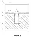
- FIG. 5is a cross-section view of the structure of FIG. 4 illustrating a copper fill process
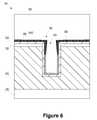
- FIG. 6is a cross-section view of the structure of FIG. 5 illustrating a copper anneal process to form alloy regions at the corners;
- FIG. 7is a cross-section view of the structure of FIG. 6 illustrating a polishing process to remove excess copper and recess the copper at the corners.
- FIG. 1is a cross-section view of a partially completed interconnect structure 10 .
- a dielectric layer 20has been provided on a substrate 25 .
- the dielectric layermay represent an interlayer dielectric layer disposed between a device layer or metallization layer and another metallization layer.
- the dielectric layer 20may have a low dielectric coefficient, commonly referred to as a low-k dielectric.
- a low-k dielectricis Black Diamond, offered by Applied Materials, Inc.
- a hard mask layer 30is formed to provide a template for etching a recess 40 .
- the recess 40is a trench in which an interconnect line feature is being formed, however, the methods described herein may also be applied to other types of interconnects, such as via structures or dual damascene trench and via structures, where an underlying metal region is being contacted by the interconnect feature.
- the recess 40may be a trench, a via opening, or a combined trench and via opening.
- a barrier layer 50is formed to line the recess 40 .
- the barrier layer 50serves to constrain the copper used to eventually fill the recess 40 so that it does not move into the dielectric layer 20 .
- Exemplary barrier materialsinclude tantalum nitride (TaN), which may be formed by physical vapor deposition (PVD) or atomic layer deposition (ALD) processes known in the art.
- a first transition metal layer 60is formed on upper corners 70 of the recess 40 above the barrier layer 50 .
- Exemplary transition metalscould include any element in the d-block of the periodic table, which includes groups 3 to 12 on the periodic table.
- titanium (Ti)is used to form the first transition metal layer 60 .
- a plasma assisted PVD processmay be employed without a bias voltage to form the first transition metal layer 60 on the corners 70 .
- a CVD processmay be employed as an alternative to the PVD process. Because of the aspect ratio of the recess 40 , the transition metal layer 60 does not substantially cover the sidewall or bottom portions of the recess 40 .
- Stray particles of the transition metalmay be formed on the sidewall or bottom portions, but due to the lack of bias voltage to attract the particles to the bottom, the transition metal layer 60 is concentrated at the corners 70 .
- the thickness of the transition metal layer 60is about 5 to 30 angstroms.
- a second transition metal layer 80(i.e., any of the d-block metals) having a copper wettability greater than the first transition metal layer 60 is formed using a chemical vapor deposition process in FIG. 4 .
- the second transition metal layeris ruthenium (Ru), but other transition metals having relatively high wettabilities that may be used are osmium, rhodium, palladium, platinum, iridium, and niobium.
- the thickness of the second transition metal layer 80is about 10 to 25 angstroms.
- the second transition metal layer 80fully lines the recess 40 , and provides a wettable surface for a subsequent copper fill.
- a copper seed layer(not visible) is formed and the bulk copper fill is performed to form copper fill layer 90 .
- an anneal processis performed to realign the grain boundaries and increase the grain size of the copper layer 90 .
- the first transition metal layer 60forms an alloy layer 100 in the corner regions 70 with the second transition metal layer 80 .
- the annealmay be performed at temperatures between about 100-400° C. for about 0.5 to 2.0 hr.
- CMPchemical mechanical polishing
- the alloy layer 100has a reduced wettability as compared to the second transition metal layer 80 .
- the first transition metal in the alloy layer 100forms an oxide at the corner interface (e.g., TiO x ).
- the oxidecauses the copper layer 90 to dewet at the corner interface 70 .
- Crevices 110are generated at the corners 70 due to the stress assisted etch used to perform the CMP process, thereby recessing the copper 90 at the corners 70 .
- the crevices 110isolate the copper 90 from the triple point of the interconnect structure 10
- the use of the second transition metal layer 80allows an improved copper fill by increasing wettability.
- the formation of the alloy layer 100 during the copper annealprovides reduced wettability in the corner regions 70 during the CMP process, thereby recessing the copper 90 .
- the recessed copper 90improves the time-dependent dielectric breakdown (TDDB) reliability of the interconnect structure 10 , because the poor copper wettability at the trench edge retards copper diffusion to the dielectric surface, which degrades reliability.
- TDDBtime-dependent dielectric breakdown
Landscapes
- Engineering & Computer Science (AREA)
- Physics & Mathematics (AREA)
- Condensed Matter Physics & Semiconductors (AREA)
- General Physics & Mathematics (AREA)
- Computer Hardware Design (AREA)
- Microelectronics & Electronic Packaging (AREA)
- Power Engineering (AREA)
- Manufacturing & Machinery (AREA)
- Internal Circuitry In Semiconductor Integrated Circuit Devices (AREA)
Abstract
Description
Claims (15)
Priority Applications (7)
| Application Number | Priority Date | Filing Date | Title |
|---|---|---|---|
| US13/561,195US8722534B2 (en) | 2012-07-30 | 2012-07-30 | Method for reducing wettability of interconnect material at corner interface and device incorporating same |
| SG2013055843ASG196744A1 (en) | 2012-07-30 | 2013-07-22 | Method for reducing wettability of interconnect material at corner interface and device incorporating same |
| TW102126070ATWI536498B (en) | 2012-07-30 | 2013-07-22 | Method for reducing wettability of interconnect material at corner interface and device incorporating same |
| DE102013214441.5ADE102013214441B4 (en) | 2012-07-30 | 2013-07-24 | A method of reducing the wettability of bonding material at corner abutment surfaces and a device made according to the method |
| KR1020130089810AKR20140016195A (en) | 2012-07-30 | 2013-07-29 | Method for reducing wettability of interconnect material at corner interface and device incorporating same |
| CN201310325245.7ACN103579098B (en) | 2012-07-30 | 2013-07-30 | It is used for reducing wettable method and the relevant apparatus of the interface material of corner interface |
| US14/227,807US9209135B2 (en) | 2012-07-30 | 2014-03-27 | Method for reducing wettability of interconnect material at corner interface and device incorporating same |
Applications Claiming Priority (1)
| Application Number | Priority Date | Filing Date | Title |
|---|---|---|---|
| US13/561,195US8722534B2 (en) | 2012-07-30 | 2012-07-30 | Method for reducing wettability of interconnect material at corner interface and device incorporating same |
Related Child Applications (1)
| Application Number | Title | Priority Date | Filing Date |
|---|---|---|---|
| US14/227,807DivisionUS9209135B2 (en) | 2012-07-30 | 2014-03-27 | Method for reducing wettability of interconnect material at corner interface and device incorporating same |
Publications (2)
| Publication Number | Publication Date |
|---|---|
| US20140027910A1 US20140027910A1 (en) | 2014-01-30 |
| US8722534B2true US8722534B2 (en) | 2014-05-13 |
Family
ID=49994091
Family Applications (2)
| Application Number | Title | Priority Date | Filing Date |
|---|---|---|---|
| US13/561,195ActiveUS8722534B2 (en) | 2012-07-30 | 2012-07-30 | Method for reducing wettability of interconnect material at corner interface and device incorporating same |
| US14/227,807Expired - Fee RelatedUS9209135B2 (en) | 2012-07-30 | 2014-03-27 | Method for reducing wettability of interconnect material at corner interface and device incorporating same |
Family Applications After (1)
| Application Number | Title | Priority Date | Filing Date |
|---|---|---|---|
| US14/227,807Expired - Fee RelatedUS9209135B2 (en) | 2012-07-30 | 2014-03-27 | Method for reducing wettability of interconnect material at corner interface and device incorporating same |
Country Status (6)
| Country | Link |
|---|---|
| US (2) | US8722534B2 (en) |
| KR (1) | KR20140016195A (en) |
| CN (1) | CN103579098B (en) |
| DE (1) | DE102013214441B4 (en) |
| SG (1) | SG196744A1 (en) |
| TW (1) | TWI536498B (en) |
Cited By (1)
| Publication number | Priority date | Publication date | Assignee | Title |
|---|---|---|---|---|
| US10170439B1 (en) | 2017-09-29 | 2019-01-01 | Globalfoundries Inc. | Chamfering for stress reduction on passivation layer |
Families Citing this family (5)
| Publication number | Priority date | Publication date | Assignee | Title |
|---|---|---|---|---|
| US20150371925A1 (en)* | 2014-06-20 | 2015-12-24 | Intel Corporation | Through array routing for non-volatile memory |
| US9711464B2 (en) | 2015-09-23 | 2017-07-18 | International Business Machines Corporation | Semiconductor chip with anti-reverse engineering function |
| US9960240B2 (en) | 2015-10-21 | 2018-05-01 | International Business Machines Corporation | Low resistance contact structures for trench structures |
| US10304773B2 (en) | 2015-10-21 | 2019-05-28 | International Business Machines Corporation | Low resistance contact structures including a copper fill for trench structures |
| US11004735B2 (en) | 2018-09-14 | 2021-05-11 | International Business Machines Corporation | Conductive interconnect having a semi-liner and no top surface recess |
Citations (3)
| Publication number | Priority date | Publication date | Assignee | Title |
|---|---|---|---|---|
| US20060211236A1 (en)* | 2003-02-17 | 2006-09-21 | Alchimer S.A. 15, Rue Du Buisson Aux Fraises- Zi | Surface-coating method, production of microelectronic interconnections using said method and integrated circuits |
| US7365005B1 (en)* | 2002-05-20 | 2008-04-29 | Gadgil Prasad N | Method for filling of a recessed structure of a semiconductor device |
| US7811925B1 (en)* | 2005-10-13 | 2010-10-12 | Novellus Systems, Inc. | Capping before barrier-removal IC fabrication method |
Family Cites Families (6)
| Publication number | Priority date | Publication date | Assignee | Title |
|---|---|---|---|---|
| KR960010056B1 (en)* | 1992-12-10 | 1996-07-25 | 삼성전자 주식회사 | Semiconductor device and manufacturing method |
| JPH09153470A (en)* | 1995-12-01 | 1997-06-10 | Hitachi Ltd | Semiconductor device film forming method |
| JPH1064902A (en)* | 1996-07-12 | 1998-03-06 | Applied Materials Inc | Aluminum film forming method and film forming apparatus |
| US7799674B2 (en) | 2008-02-19 | 2010-09-21 | Asm Japan K.K. | Ruthenium alloy film for copper interconnects |
| US8336204B2 (en)* | 2009-07-27 | 2012-12-25 | International Business Machines Corporation | Formation of alloy liner by reaction of diffusion barrier and seed layer for interconnect application |
| US7956463B2 (en) | 2009-09-16 | 2011-06-07 | International Business Machines Corporation | Large grain size conductive structure for narrow interconnect openings |
- 2012
- 2012-07-30USUS13/561,195patent/US8722534B2/enactiveActive
- 2013
- 2013-07-22SGSG2013055843Apatent/SG196744A1/enunknown
- 2013-07-22TWTW102126070Apatent/TWI536498B/ennot_activeIP Right Cessation
- 2013-07-24DEDE102013214441.5Apatent/DE102013214441B4/enactiveActive
- 2013-07-29KRKR1020130089810Apatent/KR20140016195A/ennot_activeWithdrawn
- 2013-07-30CNCN201310325245.7Apatent/CN103579098B/ennot_activeExpired - Fee Related
- 2014
- 2014-03-27USUS14/227,807patent/US9209135B2/ennot_activeExpired - Fee Related
Patent Citations (3)
| Publication number | Priority date | Publication date | Assignee | Title |
|---|---|---|---|---|
| US7365005B1 (en)* | 2002-05-20 | 2008-04-29 | Gadgil Prasad N | Method for filling of a recessed structure of a semiconductor device |
| US20060211236A1 (en)* | 2003-02-17 | 2006-09-21 | Alchimer S.A. 15, Rue Du Buisson Aux Fraises- Zi | Surface-coating method, production of microelectronic interconnections using said method and integrated circuits |
| US7811925B1 (en)* | 2005-10-13 | 2010-10-12 | Novellus Systems, Inc. | Capping before barrier-removal IC fabrication method |
Cited By (1)
| Publication number | Priority date | Publication date | Assignee | Title |
|---|---|---|---|---|
| US10170439B1 (en) | 2017-09-29 | 2019-01-01 | Globalfoundries Inc. | Chamfering for stress reduction on passivation layer |
Also Published As
| Publication number | Publication date |
|---|---|
| CN103579098B (en) | 2016-10-05 |
| CN103579098A (en) | 2014-02-12 |
| US9209135B2 (en) | 2015-12-08 |
| TWI536498B (en) | 2016-06-01 |
| DE102013214441B4 (en) | 2019-03-28 |
| SG196744A1 (en) | 2014-02-13 |
| US20140210088A1 (en) | 2014-07-31 |
| US20140027910A1 (en) | 2014-01-30 |
| TW201411777A (en) | 2014-03-16 |
| DE102013214441A1 (en) | 2014-02-13 |
| KR20140016195A (en) | 2014-02-07 |
Similar Documents
| Publication | Publication Date | Title |
|---|---|---|
| US7611991B2 (en) | Technique for increasing adhesion of metallization layers by providing dummy vias | |
| US9209135B2 (en) | Method for reducing wettability of interconnect material at corner interface and device incorporating same | |
| US8772158B2 (en) | Multi-layer barrier layer stacks for interconnect structures | |
| US9269615B2 (en) | Multi-layer barrier layer for interconnect structure | |
| CN100420009C (en) | Semiconductor device and opening structure in semiconductor device | |
| JP2006344965A (en) | Wiring structure, method for forming the same, and dual damascene structure | |
| US6495448B1 (en) | Dual damascene process | |
| US7348672B2 (en) | Interconnects with improved reliability | |
| US10347529B2 (en) | Interconnect structures | |
| US20240014069A1 (en) | Metal interconnect structure and method for fabricating the same | |
| US8049263B2 (en) | Semiconductor device including metal-insulator-metal capacitor and method of manufacturing same | |
| US20190304928A1 (en) | Advanced crack stop structure | |
| US7629239B2 (en) | Method of fabricating a semiconductor device with a dopant region in a lower wire | |
| US8728931B2 (en) | Multi-layer barrier layer for interconnect structure | |
| US7291557B2 (en) | Method for forming an interconnection structure for ic metallization | |
| US7687392B2 (en) | Semiconductor device having metal wiring and method for fabricating the same | |
| US10964647B2 (en) | Dielectric crack stop for advanced interconnects | |
| US20040203228A1 (en) | Method of forming a tungsten plug | |
| US20240096796A1 (en) | Integrated circuit device | |
| WO2007064471A1 (en) | A technique for increasing adhesion of metallization layers by providing dummy vias | |
| JP2012028480A (en) | Semiconductor device and manufacturing method therefor |
Legal Events
| Date | Code | Title | Description |
|---|---|---|---|
| AS | Assignment | Owner name:GLOBALFOUNDRIES INC., CAYMAN ISLANDS Free format text:ASSIGNMENT OF ASSIGNORS INTEREST;ASSIGNORS:ZHANG, XUNYUAN;KIM, HOON;RYAN, VIVIAN W.;SIGNING DATES FROM 20120719 TO 20120724;REEL/FRAME:028671/0042 | |
| STCF | Information on status: patent grant | Free format text:PATENTED CASE | |
| MAFP | Maintenance fee payment | Free format text:PAYMENT OF MAINTENANCE FEE, 4TH YEAR, LARGE ENTITY (ORIGINAL EVENT CODE: M1551) Year of fee payment:4 | |
| AS | Assignment | Owner name:WILMINGTON TRUST, NATIONAL ASSOCIATION, DELAWARE Free format text:SECURITY AGREEMENT;ASSIGNOR:GLOBALFOUNDRIES INC.;REEL/FRAME:049490/0001 Effective date:20181127 | |
| AS | Assignment | Owner name:GLOBALFOUNDRIES U.S. INC., CALIFORNIA Free format text:ASSIGNMENT OF ASSIGNORS INTEREST;ASSIGNOR:GLOBALFOUNDRIES INC.;REEL/FRAME:054633/0001 Effective date:20201022 | |
| AS | Assignment | Owner name:GLOBALFOUNDRIES INC., CAYMAN ISLANDS Free format text:RELEASE BY SECURED PARTY;ASSIGNOR:WILMINGTON TRUST, NATIONAL ASSOCIATION;REEL/FRAME:054636/0001 Effective date:20201117 | |
| AS | Assignment | Owner name:GLOBALFOUNDRIES U.S. INC., NEW YORK Free format text:RELEASE BY SECURED PARTY;ASSIGNOR:WILMINGTON TRUST, NATIONAL ASSOCIATION;REEL/FRAME:056987/0001 Effective date:20201117 | |
| MAFP | Maintenance fee payment | Free format text:PAYMENT OF MAINTENANCE FEE, 8TH YEAR, LARGE ENTITY (ORIGINAL EVENT CODE: M1552); ENTITY STATUS OF PATENT OWNER: LARGE ENTITY Year of fee payment:8 |