US8717137B2 - On-chip inductor using redistribution layer and dual-layer passivation - Google Patents
On-chip inductor using redistribution layer and dual-layer passivationDownload PDFInfo
- Publication number
- US8717137B2 US8717137B2US11/443,171US44317106AUS8717137B2US 8717137 B2US8717137 B2US 8717137B2US 44317106 AUS44317106 AUS 44317106AUS 8717137 B2US8717137 B2US 8717137B2
- Authority
- US
- United States
- Prior art keywords
- layer
- metal
- passivation
- redistribution
- metal layer
- Prior art date
- Legal status (The legal status is an assumption and is not a legal conclusion. Google has not performed a legal analysis and makes no representation as to the accuracy of the status listed.)
- Active, expires
Links
- 239000010410layerSubstances0.000titleclaimsabstractdescription235
- 238000002161passivationMethods0.000titleclaimsabstractdescription48
- 239000002355dual-layerSubstances0.000titleabstractdescription4
- 229910052751metalInorganic materials0.000claimsabstractdescription104
- 239000002184metalSubstances0.000claimsabstractdescription104
- 239000002365multiple layerSubstances0.000claimsabstractdescription5
- 239000000758substrateSubstances0.000claimsdescription13
- 150000004767nitridesChemical class0.000claimsdescription8
- 229910052782aluminiumInorganic materials0.000claimsdescription7
- XAGFODPZIPBFFR-UHFFFAOYSA-NaluminiumChemical compound[Al]XAGFODPZIPBFFR-UHFFFAOYSA-N0.000claimsdescription7
- RYGMFSIKBFXOCR-UHFFFAOYSA-NCopperChemical compound[Cu]RYGMFSIKBFXOCR-UHFFFAOYSA-N0.000claimsdescription6
- 239000004642PolyimideSubstances0.000claimsdescription6
- 229910052802copperInorganic materials0.000claimsdescription6
- 239000010949copperSubstances0.000claimsdescription6
- 239000000463materialSubstances0.000claimsdescription6
- 229920001721polyimidePolymers0.000claimsdescription6
- 238000000034methodMethods0.000abstractdescription6
- 238000010276constructionMethods0.000abstractdescription3
- 238000004806packaging method and processMethods0.000description5
- 239000003989dielectric materialSubstances0.000description3
- 238000004519manufacturing processMethods0.000description3
- 229910000679solderInorganic materials0.000description3
- 238000009792diffusion processMethods0.000description2
- 238000012545processingMethods0.000description2
- 239000000047productSubstances0.000description2
- 239000004065semiconductorSubstances0.000description2
- 229910052581Si3N4Inorganic materials0.000description1
- 239000007767bonding agentSubstances0.000description1
- 239000004020conductorSubstances0.000description1
- 230000009977dual effectEffects0.000description1
- 239000010408filmSubstances0.000description1
- 239000012467final productSubstances0.000description1
- 229910021420polycrystalline siliconInorganic materials0.000description1
- 229920005591polysiliconPolymers0.000description1
- 238000012805post-processingMethods0.000description1
- 238000007781pre-processingMethods0.000description1
- 150000003839saltsChemical class0.000description1
- HQVNEWCFYHHQES-UHFFFAOYSA-Nsilicon nitrideChemical compoundN12[Si]34N5[Si]62N3[Si]51N64HQVNEWCFYHHQES-UHFFFAOYSA-N0.000description1
- 239000010409thin filmSubstances0.000description1
Images


Classifications
- H—ELECTRICITY
- H10—SEMICONDUCTOR DEVICES; ELECTRIC SOLID-STATE DEVICES NOT OTHERWISE PROVIDED FOR
- H10D—INORGANIC ELECTRIC SEMICONDUCTOR DEVICES
- H10D1/00—Resistors, capacitors or inductors
- H10D1/20—Inductors
- H—ELECTRICITY
- H01—ELECTRIC ELEMENTS
- H01F—MAGNETS; INDUCTANCES; TRANSFORMERS; SELECTION OF MATERIALS FOR THEIR MAGNETIC PROPERTIES
- H01F17/00—Fixed inductances of the signal type
- H01F17/0006—Printed inductances
- H01F17/0013—Printed inductances with stacked layers
- H—ELECTRICITY
- H01—ELECTRIC ELEMENTS
- H01F—MAGNETS; INDUCTANCES; TRANSFORMERS; SELECTION OF MATERIALS FOR THEIR MAGNETIC PROPERTIES
- H01F41/00—Apparatus or processes specially adapted for manufacturing or assembling magnets, inductances or transformers; Apparatus or processes specially adapted for manufacturing materials characterised by their magnetic properties
- H01F41/02—Apparatus or processes specially adapted for manufacturing or assembling magnets, inductances or transformers; Apparatus or processes specially adapted for manufacturing materials characterised by their magnetic properties for manufacturing cores, coils, or magnets
- H01F41/04—Apparatus or processes specially adapted for manufacturing or assembling magnets, inductances or transformers; Apparatus or processes specially adapted for manufacturing materials characterised by their magnetic properties for manufacturing cores, coils, or magnets for manufacturing coils
- H01F41/041—Printed circuit coils
- H—ELECTRICITY
- H01—ELECTRIC ELEMENTS
- H01F—MAGNETS; INDUCTANCES; TRANSFORMERS; SELECTION OF MATERIALS FOR THEIR MAGNETIC PROPERTIES
- H01F5/00—Coils
- H—ELECTRICITY
- H01—ELECTRIC ELEMENTS
- H01L—SEMICONDUCTOR DEVICES NOT COVERED BY CLASS H10
- H01L23/00—Details of semiconductor or other solid state devices
- H01L23/52—Arrangements for conducting electric current within the device in operation from one component to another, i.e. interconnections, e.g. wires, lead frames
- H01L23/522—Arrangements for conducting electric current within the device in operation from one component to another, i.e. interconnections, e.g. wires, lead frames including external interconnections consisting of a multilayer structure of conductive and insulating layers inseparably formed on the semiconductor body
- H01L23/5227—Inductive arrangements or effects of, or between, wiring layers
- H—ELECTRICITY
- H01—ELECTRIC ELEMENTS
- H01L—SEMICONDUCTOR DEVICES NOT COVERED BY CLASS H10
- H01L24/00—Arrangements for connecting or disconnecting semiconductor or solid-state bodies; Methods or apparatus related thereto
- H01L24/01—Means for bonding being attached to, or being formed on, the surface to be connected, e.g. chip-to-package, die-attach, "first-level" interconnects; Manufacturing methods related thereto
- H01L24/10—Bump connectors ; Manufacturing methods related thereto
- H01L24/12—Structure, shape, material or disposition of the bump connectors prior to the connecting process
- H01L24/13—Structure, shape, material or disposition of the bump connectors prior to the connecting process of an individual bump connector
- H—ELECTRICITY
- H10—SEMICONDUCTOR DEVICES; ELECTRIC SOLID-STATE DEVICES NOT OTHERWISE PROVIDED FOR
- H10D—INORGANIC ELECTRIC SEMICONDUCTOR DEVICES
- H10D84/00—Integrated devices formed in or on semiconductor substrates that comprise only semiconducting layers, e.g. on Si wafers or on GaAs-on-Si wafers
- H—ELECTRICITY
- H01—ELECTRIC ELEMENTS
- H01L—SEMICONDUCTOR DEVICES NOT COVERED BY CLASS H10
- H01L2224/00—Indexing scheme for arrangements for connecting or disconnecting semiconductor or solid-state bodies and methods related thereto as covered by H01L24/00
- H01L2224/01—Means for bonding being attached to, or being formed on, the surface to be connected, e.g. chip-to-package, die-attach, "first-level" interconnects; Manufacturing methods related thereto
- H01L2224/02—Bonding areas; Manufacturing methods related thereto
- H01L2224/04—Structure, shape, material or disposition of the bonding areas prior to the connecting process
- H01L2224/05—Structure, shape, material or disposition of the bonding areas prior to the connecting process of an individual bonding area
- H01L2224/05001—Internal layers
- H01L2224/0502—Disposition
- H01L2224/05022—Disposition the internal layer being at least partially embedded in the surface
- H—ELECTRICITY
- H01—ELECTRIC ELEMENTS
- H01L—SEMICONDUCTOR DEVICES NOT COVERED BY CLASS H10
- H01L2224/00—Indexing scheme for arrangements for connecting or disconnecting semiconductor or solid-state bodies and methods related thereto as covered by H01L24/00
- H01L2224/01—Means for bonding being attached to, or being formed on, the surface to be connected, e.g. chip-to-package, die-attach, "first-level" interconnects; Manufacturing methods related thereto
- H01L2224/02—Bonding areas; Manufacturing methods related thereto
- H01L2224/04—Structure, shape, material or disposition of the bonding areas prior to the connecting process
- H01L2224/05—Structure, shape, material or disposition of the bonding areas prior to the connecting process of an individual bonding area
- H01L2224/05001—Internal layers
- H01L2224/0502—Disposition
- H01L2224/05026—Disposition the internal layer being disposed in a recess of the surface
- H01L2224/05027—Disposition the internal layer being disposed in a recess of the surface the internal layer extending out of an opening
- H—ELECTRICITY
- H01—ELECTRIC ELEMENTS
- H01L—SEMICONDUCTOR DEVICES NOT COVERED BY CLASS H10
- H01L2224/00—Indexing scheme for arrangements for connecting or disconnecting semiconductor or solid-state bodies and methods related thereto as covered by H01L24/00
- H01L2224/01—Means for bonding being attached to, or being formed on, the surface to be connected, e.g. chip-to-package, die-attach, "first-level" interconnects; Manufacturing methods related thereto
- H01L2224/02—Bonding areas; Manufacturing methods related thereto
- H01L2224/04—Structure, shape, material or disposition of the bonding areas prior to the connecting process
- H01L2224/05—Structure, shape, material or disposition of the bonding areas prior to the connecting process of an individual bonding area
- H01L2224/05001—Internal layers
- H01L2224/05099—Material
- H01L2224/051—Material with a principal constituent of the material being a metal or a metalloid, e.g. boron [B], silicon [Si], germanium [Ge], arsenic [As], antimony [Sb], tellurium [Te] and polonium [Po], and alloys thereof
- H01L2224/05117—Material with a principal constituent of the material being a metal or a metalloid, e.g. boron [B], silicon [Si], germanium [Ge], arsenic [As], antimony [Sb], tellurium [Te] and polonium [Po], and alloys thereof the principal constituent melting at a temperature of greater than or equal to 400°C and less than 950°C
- H01L2224/05124—Aluminium [Al] as principal constituent
- H—ELECTRICITY
- H01—ELECTRIC ELEMENTS
- H01L—SEMICONDUCTOR DEVICES NOT COVERED BY CLASS H10
- H01L2224/00—Indexing scheme for arrangements for connecting or disconnecting semiconductor or solid-state bodies and methods related thereto as covered by H01L24/00
- H01L2224/01—Means for bonding being attached to, or being formed on, the surface to be connected, e.g. chip-to-package, die-attach, "first-level" interconnects; Manufacturing methods related thereto
- H01L2224/02—Bonding areas; Manufacturing methods related thereto
- H01L2224/04—Structure, shape, material or disposition of the bonding areas prior to the connecting process
- H01L2224/05—Structure, shape, material or disposition of the bonding areas prior to the connecting process of an individual bonding area
- H01L2224/05001—Internal layers
- H01L2224/05099—Material
- H01L2224/051—Material with a principal constituent of the material being a metal or a metalloid, e.g. boron [B], silicon [Si], germanium [Ge], arsenic [As], antimony [Sb], tellurium [Te] and polonium [Po], and alloys thereof
- H01L2224/05138—Material with a principal constituent of the material being a metal or a metalloid, e.g. boron [B], silicon [Si], germanium [Ge], arsenic [As], antimony [Sb], tellurium [Te] and polonium [Po], and alloys thereof the principal constituent melting at a temperature of greater than or equal to 950°C and less than 1550°C
- H01L2224/05147—Copper [Cu] as principal constituent
- H—ELECTRICITY
- H01—ELECTRIC ELEMENTS
- H01L—SEMICONDUCTOR DEVICES NOT COVERED BY CLASS H10
- H01L2224/00—Indexing scheme for arrangements for connecting or disconnecting semiconductor or solid-state bodies and methods related thereto as covered by H01L24/00
- H01L2224/01—Means for bonding being attached to, or being formed on, the surface to be connected, e.g. chip-to-package, die-attach, "first-level" interconnects; Manufacturing methods related thereto
- H01L2224/02—Bonding areas; Manufacturing methods related thereto
- H01L2224/04—Structure, shape, material or disposition of the bonding areas prior to the connecting process
- H01L2224/05—Structure, shape, material or disposition of the bonding areas prior to the connecting process of an individual bonding area
- H01L2224/0554—External layer
- H01L2224/0556—Disposition
- H01L2224/05571—Disposition the external layer being disposed in a recess of the surface
- H01L2224/05572—Disposition the external layer being disposed in a recess of the surface the external layer extending out of an opening
- H—ELECTRICITY
- H01—ELECTRIC ELEMENTS
- H01L—SEMICONDUCTOR DEVICES NOT COVERED BY CLASS H10
- H01L2224/00—Indexing scheme for arrangements for connecting or disconnecting semiconductor or solid-state bodies and methods related thereto as covered by H01L24/00
- H01L2224/01—Means for bonding being attached to, or being formed on, the surface to be connected, e.g. chip-to-package, die-attach, "first-level" interconnects; Manufacturing methods related thereto
- H01L2224/02—Bonding areas; Manufacturing methods related thereto
- H01L2224/04—Structure, shape, material or disposition of the bonding areas prior to the connecting process
- H01L2224/05—Structure, shape, material or disposition of the bonding areas prior to the connecting process of an individual bonding area
- H01L2224/0554—External layer
- H01L2224/05599—Material
- H01L2224/056—Material with a principal constituent of the material being a metal or a metalloid, e.g. boron [B], silicon [Si], germanium [Ge], arsenic [As], antimony [Sb], tellurium [Te] and polonium [Po], and alloys thereof
- H—ELECTRICITY
- H01—ELECTRIC ELEMENTS
- H01L—SEMICONDUCTOR DEVICES NOT COVERED BY CLASS H10
- H01L2224/00—Indexing scheme for arrangements for connecting or disconnecting semiconductor or solid-state bodies and methods related thereto as covered by H01L24/00
- H01L2224/01—Means for bonding being attached to, or being formed on, the surface to be connected, e.g. chip-to-package, die-attach, "first-level" interconnects; Manufacturing methods related thereto
- H01L2224/10—Bump connectors; Manufacturing methods related thereto
- H01L2224/12—Structure, shape, material or disposition of the bump connectors prior to the connecting process
- H01L2224/13—Structure, shape, material or disposition of the bump connectors prior to the connecting process of an individual bump connector
- H01L2224/13001—Core members of the bump connector
- H01L2224/13099—Material
- H—ELECTRICITY
- H01—ELECTRIC ELEMENTS
- H01L—SEMICONDUCTOR DEVICES NOT COVERED BY CLASS H10
- H01L2224/00—Indexing scheme for arrangements for connecting or disconnecting semiconductor or solid-state bodies and methods related thereto as covered by H01L24/00
- H01L2224/01—Means for bonding being attached to, or being formed on, the surface to be connected, e.g. chip-to-package, die-attach, "first-level" interconnects; Manufacturing methods related thereto
- H01L2224/10—Bump connectors; Manufacturing methods related thereto
- H01L2224/15—Structure, shape, material or disposition of the bump connectors after the connecting process
- H01L2224/16—Structure, shape, material or disposition of the bump connectors after the connecting process of an individual bump connector
- H—ELECTRICITY
- H01—ELECTRIC ELEMENTS
- H01L—SEMICONDUCTOR DEVICES NOT COVERED BY CLASS H10
- H01L23/00—Details of semiconductor or other solid state devices
- H01L23/52—Arrangements for conducting electric current within the device in operation from one component to another, i.e. interconnections, e.g. wires, lead frames
- H01L23/522—Arrangements for conducting electric current within the device in operation from one component to another, i.e. interconnections, e.g. wires, lead frames including external interconnections consisting of a multilayer structure of conductive and insulating layers inseparably formed on the semiconductor body
- H01L23/525—Arrangements for conducting electric current within the device in operation from one component to another, i.e. interconnections, e.g. wires, lead frames including external interconnections consisting of a multilayer structure of conductive and insulating layers inseparably formed on the semiconductor body with adaptable interconnections
- H—ELECTRICITY
- H01—ELECTRIC ELEMENTS
- H01L—SEMICONDUCTOR DEVICES NOT COVERED BY CLASS H10
- H01L2924/00—Indexing scheme for arrangements or methods for connecting or disconnecting semiconductor or solid-state bodies as covered by H01L24/00
- H01L2924/01—Chemical elements
- H01L2924/01013—Aluminum [Al]
- H—ELECTRICITY
- H01—ELECTRIC ELEMENTS
- H01L—SEMICONDUCTOR DEVICES NOT COVERED BY CLASS H10
- H01L2924/00—Indexing scheme for arrangements or methods for connecting or disconnecting semiconductor or solid-state bodies as covered by H01L24/00
- H01L2924/01—Chemical elements
- H01L2924/01029—Copper [Cu]
- H—ELECTRICITY
- H01—ELECTRIC ELEMENTS
- H01L—SEMICONDUCTOR DEVICES NOT COVERED BY CLASS H10
- H01L2924/00—Indexing scheme for arrangements or methods for connecting or disconnecting semiconductor or solid-state bodies as covered by H01L24/00
- H01L2924/01—Chemical elements
- H01L2924/01033—Arsenic [As]
- H—ELECTRICITY
- H01—ELECTRIC ELEMENTS
- H01L—SEMICONDUCTOR DEVICES NOT COVERED BY CLASS H10
- H01L2924/00—Indexing scheme for arrangements or methods for connecting or disconnecting semiconductor or solid-state bodies as covered by H01L24/00
- H01L2924/01—Chemical elements
- H01L2924/01082—Lead [Pb]
- H—ELECTRICITY
- H01—ELECTRIC ELEMENTS
- H01L—SEMICONDUCTOR DEVICES NOT COVERED BY CLASS H10
- H01L2924/00—Indexing scheme for arrangements or methods for connecting or disconnecting semiconductor or solid-state bodies as covered by H01L24/00
- H01L2924/013—Alloys
- H01L2924/014—Solder alloys
- H—ELECTRICITY
- H01—ELECTRIC ELEMENTS
- H01L—SEMICONDUCTOR DEVICES NOT COVERED BY CLASS H10
- H01L2924/00—Indexing scheme for arrangements or methods for connecting or disconnecting semiconductor or solid-state bodies as covered by H01L24/00
- H01L2924/10—Details of semiconductor or other solid state devices to be connected
- H01L2924/11—Device type
- H01L2924/14—Integrated circuits
- H—ELECTRICITY
- H01—ELECTRIC ELEMENTS
- H01L—SEMICONDUCTOR DEVICES NOT COVERED BY CLASS H10
- H01L2924/00—Indexing scheme for arrangements or methods for connecting or disconnecting semiconductor or solid-state bodies as covered by H01L24/00
- H01L2924/19—Details of hybrid assemblies other than the semiconductor or other solid state devices to be connected
- H01L2924/1901—Structure
- H01L2924/1904—Component type
- H01L2924/19042—Component type being an inductor
- H—ELECTRICITY
- H01—ELECTRIC ELEMENTS
- H01L—SEMICONDUCTOR DEVICES NOT COVERED BY CLASS H10
- H01L2924/00—Indexing scheme for arrangements or methods for connecting or disconnecting semiconductor or solid-state bodies as covered by H01L24/00
- H01L2924/30—Technical effects
- H01L2924/301—Electrical effects
- H01L2924/30107—Inductance
- H—ELECTRICITY
- H01—ELECTRIC ELEMENTS
- H01L—SEMICONDUCTOR DEVICES NOT COVERED BY CLASS H10
- H01L2924/00—Indexing scheme for arrangements or methods for connecting or disconnecting semiconductor or solid-state bodies as covered by H01L24/00
- H01L2924/30—Technical effects
- H01L2924/301—Electrical effects
- H01L2924/3011—Impedance
Definitions
- the present inventionis related to on-chip passive devices, such as on-chip inductors.
- An example passive deviceis an inductor.
- the inductoris a key passive element in circuit applications, such as voltage controlled oscillators, low noise amplifiers, mixers and power amplifiers.
- Qquality factor
- On-chip inductorsare usually implemented by spiral structures fabricated on metal layers.
- the inductorscan have different shapes, such as square, circular, or octagonal, they can be symmetric or non-symmetric, and/or they can be implemented with a single metal layer or multiple metal layers.
- existing metal interconnect layersare used in a concentric ring-type structure to maximize inductance.
- the metal layersare also used for signal routing or power bussing.
- the Q factor for an inductorincreases the further it is placed from a substrate on which the chip is formed.
- a key factor that limits the construction of inductors using a top metal layer of the chipis the necessity to insulate the top metal layer of the chip from the outside environment (i.e., moisture, salt, scratch, etc) through films such as silicon nitride.
- the additional metal layerswill substantially add cost to the final product (e.g., 6-7% of the overall “cost” of the product per additional metal layer).
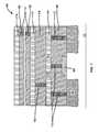
- FIG. 1shows a cross-section of a portion of a chip.
- FIGS. 2 and 3show perspective and bottom views of a bump or flip chip packaging arrangement, according to one embodiment of the present invention.
- FIGS. 4 , 5 , and 6show cross-sectional views of a bump structure, according to various embodiments of the present invention.
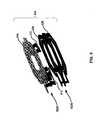
- FIGS. 7 and 8show cross-sectional side and cut-away perspective views of an inductor formed in a redistribution layer of a flip-chip, according to one embodiment of the present invention.
- FIG. 9shows a transformer partially formed in a redistribution layer of a flip-chip, according to one embodiment of the present invention.
- FIG. 10shows a high Q spiral inductor, according to one embodiment of the present invention.
- FIGS. 11 , 12 , 13 , and 14show various arrangements of two layer inductors, according to various embodiments of the present invention.
- FIG. 15shows a flowchart depicting a method for forming an on-chip inductor, according to one embodiment of the present invention.
- FIG. 16shows a transformer, according to one embodiment of the present invention.
- references in the specification to “one embodiment”, “an embodiment”, “an example embodiment”, etc.,indicate that the embodiment described may include a particular feature, structure, or characteristic, but every embodiment may not necessarily include the particular feature, structure, or characteristic. Moreover, such phrases are not necessarily referring to the same embodiment. Further, when a particular feature, structure, or characteristic is described in connection with an embodiment, it is submitted that it is within the knowledge of one skilled in the art to affect such feature, structure, or characteristic in connection with other embodiments whether or not explicitly described.
- One embodiment of the present inventionprovides a system and method that utilize a redistribution layer in a flip-chip or wirebond package, which is also used to route signals to bumps, as a layer for the construction of an on-chip inductor or a layer of a multiple-layer on-chip inductor.
- the redistribution layeris surrounded by dual-layer passivation to protect it, and the inductor formed thereby, from the environment and isolate it, and the inductor formed thereby, from the metal layer beneath it.
- FIG. 1shows a cross-section of a portion 100 of a chip.
- Portion 100includes a substrate 102 having diffusion regions 104 .
- a polysilicon 106is formed on the substrate 102 between the diffusion regions 104 .
- a first dielectric layer 108(e.g., a passivation layer) is formed between substrate 102 and a first metal layer 110 .
- Connections 112are formed between first metal layer 110 and substrate 102 through an opening (e.g., a channel or via) in first dielectric layer 108 .
- additional metal layers 114 and 116 and alternating additional dielectric layers 118 , 120 , and 122are formed, along with connections 112 between the metal layers and through openings in respective ones of the dielectric layers.
- an inductor(not shown) or a layer of an inductor (not shown) can be formed in one of the metal layers.
- inductorsexperience reduced Q factor and increase resistance the closer they are located to substrate 102 , for example due to eddy currents.
- metal layer 116the highest metal layer of a chip, e.g., metal layer 116 , is the most desirable layer on which to form an inductor.
- FIGS. 2 and 3show perspective and bottom views of a bump or flip chip packaging arrangement 200 , according to one embodiment of the present invention.
- Flip chip package 200includes an array of bumps 202 in a surface 204 .
- Flip-chipsare considered very high performance devices.
- a flip chipis a leadless, monolithic structure that contains an integrated circuit designed to electrically and mechanically interconnect to a circuit. Connection is made to bump contacts 202 , which may be covered with a conductive bonding agent (not shown), on the face 204 of the circuit.
- packaging 200is considered a ball grid array (BGA) version of a flip chip package.
- BGA-Flip Chipan integrated circuit surface 204 has an area array of solder balls 202 that are attached to the bottom side of a substrate 206 that also includes signal and power routing layers.
- FIGS. 4 , 5 , and 6show cross-sectional views of bump structures 402 , 502 , and 602 , respectively, of a flip-chip, according to various embodiments of the present invention.
- bump structure 402includes a metal redistribution layer 410 (e.g., made from aluminum or copper) (hereinafter, the terms redistribution layer and metal redistribution layer will be used interchangeably) coupled to a top metal layer 412 of a chip.
- the redistribution and top metal layers 410 and 412are encapsulated in first and second layers of passivation 414 and 416 .
- each passivation layer 414 and 416is formed through one or more layers of similar or different dielectrics, discussed in more detail below.
- a solder ball 418is formed on an under bump metal layer 420 , which under bump metal layer 420 is formed on metal distribution layer 410 .
- redistribution layer 410is a thin film routing layer formed primarily from, for example, aluminum or copper. Redistribution layer 410 can be used to route signals and provide for distributed power and ground. In one example, redistribution layer 410 can vary in thickness from about 1 to 3 microns and have a width of from about 12-100 microns, depending on the specific design requirements.
- FIG. 5shows a redistribution layer 510 formed on a top metal layer 512 through an opening in a first passivation layer 514 .
- a second passivation layer 516is formed over first passivation layer 514 and redistribution layer 510 .
- a bump metal layer 520is formed to connect a bump 518 and redistribution layer 510 . The connection is made through forming of bump metal layer 520 on top of and through an opening in second passivation layer 516 .
- first passivation layer 514is formed with nitride and second passivation layer 516 is formed with polyimide.
- FIG. 6shows a redistribution layer 610 formed on a top metal layer 612 through an opening in a first passivation layer 614 .
- a second passivation layer 616is formed over first passivation layer 614 and redistribution layer 610 .
- a bump metal layer 620is formed to connect a bump 618 and redistribution layer 610 . The connection is made through forming of bump metal layer 620 on top of and through an opening in second passivation layer 616 .
- first and second passivation layers 614 and 616are both formed with nitride.
- FIGS. 7 and 8show cross-sectional side and cut-away perspective views of an inductor 722 formed in a redistribution layer 710 , according to one embodiment of the present invention.
- a metal redistribution layer 710which is already present in flip-chip packaging for routing of signals and power, is also used to form an on-chip inductor 722 . This can be done because metal distribution layer 710 is encapsulated within two layers of passivation 714 and 716 to isolate it from metal routing layers below (not shown) and the environment from above.
- FIGS. 7 and 8essentially show the bump structure from either FIG. 4 , 5 , or 6 , but without the under bump metal layer 420 / 520 / 620 and the solder ball 418 / 518 / 618 .
- inductor 722is a single loop inductor formed on redistribution layer 710 . It is to be appreciated that inductors having multiple loops and/or formed on multiple layers are also contemplated within the scope of the present invention, as discussed below. As shown, two nodes or ends 723 of inductor 722 extend through dielectric layer 714 to contact top metal layer 712 . Openings formed in each of redistribution layer 710 and contact top metal layer 712 include dielectric material 708 and 718 , respectively. Dielectric material 708 and 718 can, in one example, be similar to the material used to form first and second passivation layers 714 and 716 .
- passivation layers 714 and 716 , and dielectric portions 708 and 718can be made from either a single material or a combination of materials, for example oxide, nitride, oxynitride, polyimide, etc.
- performance of inductor 722 using this metal redistribution layer 710is comparable to or better than using an additional top metal routing layer of FIG. 1 , without the additional chip “cost.” This is because real estate and processing steps of the chip can be reduced through the use of already existing redistribution layer 710 and dual passivation layers 714 and 716 . It is to be appreciated that because redistribution layer 710 is always the farthest metal layer from a substrate (not shown), on which the chip is formed, redistribution layer 710 provides the best Q factor of any location on the chip for the on-chip inductor 722 .
- a thickness of redistribution metal layer 710can be increased to, in turn, increase the Q factor of the resulting inductor 722 .
- Qis proportional to I/R so as resistance goes down, Q increases.
- resistancegoes down based on there being more cross section area to carry a current. This allows for the proportional increase in Q.
- FIG. 9shows a transformer 924 partially formed in a redistribution layer 910 , according to one embodiment of the present invention.
- transformer 924can be designed with about a 27 ⁇ m-wide metal trace.
- Transformer 924is formed from two inductors 922 A and 922 B.
- Inductor 922 Ais formed in a metal redistribution layer 910 and a top metal layer 912 and inductor 922 B is formed in second and third metal layers 926 and 928 , respectively.
- second and third metal layers 926 and 928are closer to a substrate (not shown) than layers 910 and 912 , similar to the configuration shown in FIG. 1 .
- FIG. 16shows a transformer 1624 , according to one embodiment of the present invention.
- Transformer 1624is formed from two inductors 1622 A and 1622 B. Both inductors 1622 A and 1622 B are formed on a same metal layer, for example in a metal redistribution layer 1610 . It is to be appreciated, another metal layer could also be used as the single metal layer in which transformer 1624 is formed.
- FIG. 10shows a high Q spiral inductor 1022 , according to one embodiment of the present invention.
- Inductor 1022is constructed from multiple inductor layers 1022 A- 1022 D, each layer being constructed in a respective redistribution or metal layer 1010 , 1012 , 1026 , and 1028 .
- a value of the inductance of inductor 1022is determined based on calculating a series inductance comprised of inductors 1022 A- 1022 D.
- layer 1010is a metal redistribution layer of a flip-chip arrangement.
- FIGS. 11 , 12 , 13 , and 14show various arrangements of two layer inductors 1122 , 1222 , 1322 , and 1422 that exhibit similar inductor characteristics, however with different manufacturing costs, according to various embodiments of the present invention.
- FIG. 11is similar to FIG. 1
- FIG. 12is similar to FIGS. 1 and 11 with an extra thick metal layer
- FIGS. 13 and 14are similar to FIGS. 7 and 8 .
- FIG. 11shows an inductor 1122 comprised of a first metal layer 1142 and a second metal layer 1144 that are separated by a first dielectric layer 1146 .
- a second dielectric layer 1148is formed over first metal layer 1142 and first dielectric layer 1146 .
- the thickness of metal layer 1142is, for example, about 9000 ⁇ and exhibits a conductivity of about 5 ⁇ 10 7 (s/m).
- FIG. 12shows an inductor 1222 comprised of a first metal layer 1242 (e.g., an extra thick metal layer) and a second metal layer 1244 that are separated by a first dielectric layer 1246 .
- a second dielectric layer 1248is formed over first metal layer 1242 and first dielectric layer 1246 .
- the thickness of metal layer 1242is, for example, about 33000 ⁇ and exhibits a conductivity of about 5.88 ⁇ 10 7 (s/m).
- FIG. 13shows an inductor 1322 comprised of a first metal layer 1310 (e.g., a metal redistribution layer) and a second metal layer 1312 .
- First metal layer 1310is surrounded by a passivation layer 1316 and second metal layer 1312 is surrounded by a passivation layer 1314 .
- first metal layer 1310is formed of aluminum.
- the thickness of aluminum layer 1310is, for example, 14000 ⁇ and exhibits a conductivity of about 3.28 ⁇ 10 7 (s/m).
- FIG. 14shows an inductor 1422 comprised of a first metal layer 1410 (e.g., a metal redistribution layer) and a second metal layer 1412 .
- First metal layer 1410is surrounded by a passivation layer 1416 and second metal layer 1412 is surrounded by a passivation layer 1414 .
- first metal layer 1410is formed of copper.
- the thickness of copper layer 1410is, for example, 9000 ⁇ and exhibits a conductivity of about 5.05 ⁇ 10 7 (s/m).
- FIG. 15shows a flowchart depicting a method 1500 to form a on-chip inductor, according to one embodiment of the present invention.
- the standard pre and post processing steps occurring during normal semiconductor manufacturehave been left out for convenience. However, a skilled artisan will understand when these steps can take place based on reading and understanding the description.
- a metal layeris formed. In one example, this can be a top metal layer of a chip already having several metal and dielectric layers formed on a substrate.
- a first passivation layeris formed over the metal layer. In various examples, different materials can be used for the passivation layer, for example oxide, nitride, oxynitride, polyimide, etc.
- an openingis formed through the first passivation layer to the metal layer. In one example, multiple openings can be formed for multiple connections between metal layers and/or for multiple nodes of an inductor (discussed below, and see, e.g., FIGS. 7 and 8 ).
- a redistribution layeris formed on the first passivation layer and through the opening in the first passivation layer, such that the redistribution layer contacts the first metal layer.
- the redistribution layerwill have a generally stepped shape.
- the redistribution layercan be any substantially conductive material, such as aluminum or copper, although the use of aluminum is desired.
- a second passivation layeris formed over the redistribution layer.
- the inductoris formed in the redistribution layer. A node or end of the inductor is the portion of the redistribution layer formed through the opening in the first passivation layer, as discussed above. If the inductor has two nodes or ends, they would correspond to additional portions of the redistribution layer that is formed through additional openings in the first passivation layer.
Landscapes
- Engineering & Computer Science (AREA)
- Power Engineering (AREA)
- Microelectronics & Electronic Packaging (AREA)
- Computer Hardware Design (AREA)
- Physics & Mathematics (AREA)
- Condensed Matter Physics & Semiconductors (AREA)
- General Physics & Mathematics (AREA)
- Manufacturing & Machinery (AREA)
- Semiconductor Integrated Circuits (AREA)
- Internal Circuitry In Semiconductor Integrated Circuit Devices (AREA)
Abstract
Description
Claims (20)
Priority Applications (2)
| Application Number | Priority Date | Filing Date | Title |
|---|---|---|---|
| US11/443,171US8717137B2 (en) | 2006-05-31 | 2006-05-31 | On-chip inductor using redistribution layer and dual-layer passivation |
| US14/246,579US20140299964A1 (en) | 2006-05-31 | 2014-04-07 | On-chip inductor using redistribution layer and dual-layer passiviation |
Applications Claiming Priority (1)
| Application Number | Priority Date | Filing Date | Title |
|---|---|---|---|
| US11/443,171US8717137B2 (en) | 2006-05-31 | 2006-05-31 | On-chip inductor using redistribution layer and dual-layer passivation |
Related Child Applications (1)
| Application Number | Title | Priority Date | Filing Date |
|---|---|---|---|
| US14/246,579ContinuationUS20140299964A1 (en) | 2006-05-31 | 2014-04-07 | On-chip inductor using redistribution layer and dual-layer passiviation |
Publications (2)
| Publication Number | Publication Date |
|---|---|
| US20070279176A1 US20070279176A1 (en) | 2007-12-06 |
| US8717137B2true US8717137B2 (en) | 2014-05-06 |
Family
ID=38789424
Family Applications (2)
| Application Number | Title | Priority Date | Filing Date |
|---|---|---|---|
| US11/443,171Active2030-12-11US8717137B2 (en) | 2006-05-31 | 2006-05-31 | On-chip inductor using redistribution layer and dual-layer passivation |
| US14/246,579AbandonedUS20140299964A1 (en) | 2006-05-31 | 2014-04-07 | On-chip inductor using redistribution layer and dual-layer passiviation |
Family Applications After (1)
| Application Number | Title | Priority Date | Filing Date |
|---|---|---|---|
| US14/246,579AbandonedUS20140299964A1 (en) | 2006-05-31 | 2014-04-07 | On-chip inductor using redistribution layer and dual-layer passiviation |
Country Status (1)
| Country | Link |
|---|---|
| US (2) | US8717137B2 (en) |
Families Citing this family (17)
| Publication number | Priority date | Publication date | Assignee | Title |
|---|---|---|---|---|
| US7391107B2 (en)* | 2005-08-18 | 2008-06-24 | Infineon Technologies Ag | Signal routing on redistribution layer |
| US8242872B2 (en)* | 2007-05-18 | 2012-08-14 | Globalfoundries Singapore Pte. Ltd. | Transformer with effective high turn ratio |
| US8860544B2 (en)* | 2007-06-26 | 2014-10-14 | Mediatek Inc. | Integrated inductor |
| US20100052839A1 (en)* | 2008-09-04 | 2010-03-04 | Koen Mertens | Transformers and Methods of Manufacture Thereof |
| US20110133308A1 (en)* | 2009-05-22 | 2011-06-09 | Chan Kuei-Ti | Semiconductor device with oxide define pattern |
| US20100295150A1 (en)* | 2009-05-22 | 2010-11-25 | Chan Kuei-Ti | Semiconductor device with oxide define dummy feature |
| US20120249107A1 (en)* | 2011-04-01 | 2012-10-04 | Cowley Nicholas P | Coupled inductor to facilitate integrated power delivery |
| US9666238B2 (en) | 2011-05-12 | 2017-05-30 | Rambus Inc. | Stacked DRAM device and method of manufacture |
| JP2013229455A (en)* | 2012-04-26 | 2013-11-07 | Renesas Electronics Corp | Semiconductor device and method for manufacturing the same |
| US9035421B2 (en)* | 2013-03-01 | 2015-05-19 | Qualcomm Incorporated | High quality factor inductor implemented in wafer level packaging (WLP) |
| CN108807208B (en)* | 2013-03-25 | 2023-06-23 | 瑞萨电子株式会社 | Semiconductor device |
| JP6235353B2 (en) | 2014-01-22 | 2017-11-22 | ルネサスエレクトロニクス株式会社 | Manufacturing method of semiconductor device |
| US9245940B2 (en)* | 2014-02-12 | 2016-01-26 | Qualcomm Incorporated | Inductor design on floating UBM balls for wafer level package (WLP) |
| US11121699B2 (en) | 2019-02-19 | 2021-09-14 | Qualcomm Incorporated | Wideband filter with resonators and inductors |
| US20240203871A1 (en)* | 2022-12-14 | 2024-06-20 | Qualcomm Incorporated | Integrated circuit bump integrated with tcoil |
| US20240321729A1 (en)* | 2023-03-20 | 2024-09-26 | Qualcomm Incorporated | Integrated redistribution layer inductors |
| CN119891990A (en)* | 2025-03-28 | 2025-04-25 | 深圳市晶扬电子有限公司 | Heterogeneous integrated filter structure with transient voltage protection and manufacturing method |
Citations (5)
| Publication number | Priority date | Publication date | Assignee | Title |
|---|---|---|---|---|
| US6355535B2 (en)* | 1998-08-07 | 2002-03-12 | Winbond Electronics Corp. | Method and structure of manufacturing a high-Q inductor with an air trench |
| US6636139B2 (en)* | 2001-09-10 | 2003-10-21 | Taiwan Semiconductor Manufacturing Company | Structure to reduce the degradation of the Q value of an inductor caused by via resistance |
| US6903644B2 (en)* | 2003-07-28 | 2005-06-07 | Taiwan Semiconductor Manufacturing Company, Ltd. | Inductor device having improved quality factor |
| US20070126543A1 (en)* | 2005-10-12 | 2007-06-07 | Ta-Hsun Yeh | Integrated inductor |
| US7459761B2 (en)* | 1998-12-21 | 2008-12-02 | Megica Corporation | High performance system-on-chip using post passivation process |
Family Cites Families (5)
| Publication number | Priority date | Publication date | Assignee | Title |
|---|---|---|---|---|
| TW515054B (en)* | 2001-06-13 | 2002-12-21 | Via Tech Inc | Flip chip pad arrangement on chip for reduction of impedance |
| US7141883B2 (en)* | 2002-10-15 | 2006-11-28 | Silicon Laboratories Inc. | Integrated circuit package configuration incorporating shielded circuit element structure |
| US7473999B2 (en)* | 2005-09-23 | 2009-01-06 | Megica Corporation | Semiconductor chip and process for forming the same |
| US20110156260A1 (en)* | 2009-12-28 | 2011-06-30 | Yu-Hua Huang | Pad structure and integrated circuit chip with such pad structure |
| US8884441B2 (en)* | 2013-02-18 | 2014-11-11 | Taiwan Semiconductor Manufacturing Co., Ltd. | Process of ultra thick trench etch with multi-slope profile |
- 2006
- 2006-05-31USUS11/443,171patent/US8717137B2/enactiveActive
- 2014
- 2014-04-07USUS14/246,579patent/US20140299964A1/ennot_activeAbandoned
Patent Citations (5)
| Publication number | Priority date | Publication date | Assignee | Title |
|---|---|---|---|---|
| US6355535B2 (en)* | 1998-08-07 | 2002-03-12 | Winbond Electronics Corp. | Method and structure of manufacturing a high-Q inductor with an air trench |
| US7459761B2 (en)* | 1998-12-21 | 2008-12-02 | Megica Corporation | High performance system-on-chip using post passivation process |
| US6636139B2 (en)* | 2001-09-10 | 2003-10-21 | Taiwan Semiconductor Manufacturing Company | Structure to reduce the degradation of the Q value of an inductor caused by via resistance |
| US6903644B2 (en)* | 2003-07-28 | 2005-06-07 | Taiwan Semiconductor Manufacturing Company, Ltd. | Inductor device having improved quality factor |
| US20070126543A1 (en)* | 2005-10-12 | 2007-06-07 | Ta-Hsun Yeh | Integrated inductor |
Non-Patent Citations (1)
| Title |
|---|
| Treleaven et al , "Integrated Circuit Passive Components." Whitepapers, Chipworks, http://www.chipworks.com.tw/resources/whitepapers/ IC Passives.pdf, 4 pages, date unknown, last viewed Jan. 31, 2007. |
Also Published As
| Publication number | Publication date |
|---|---|
| US20140299964A1 (en) | 2014-10-09 |
| US20070279176A1 (en) | 2007-12-06 |
Similar Documents
| Publication | Publication Date | Title |
|---|---|---|
| US8717137B2 (en) | On-chip inductor using redistribution layer and dual-layer passivation | |
| JP3580803B2 (en) | Semiconductor device | |
| US7598836B2 (en) | Multilayer winding inductor | |
| TWI721265B (en) | Semiconductor devices with back-side coils for wireless signal and power coupling | |
| US20080203527A1 (en) | Semiconductor device having gate electrode connection to wiring layer | |
| US20030173668A1 (en) | Semiconductor device having a bond pad and method therefor | |
| KR20090131255A (en) | Circuit device and method of manufacturing the circuit device | |
| TWI796910B (en) | Multilayer-type on-chip inductor structure | |
| CN111755415B (en) | Peaking inductor embedded in T-coil | |
| WO2004070746A1 (en) | Spiral inductor and transformer | |
| US20130256886A1 (en) | Semiconductor device | |
| US12107043B2 (en) | Multilayer-type on-chip inductor structure | |
| US20220375885A1 (en) | Flip-chip ball grid array-type integrated circuit package for very high frequency operation | |
| US6740965B2 (en) | Flip-chip package substrate | |
| KR20050022321A (en) | A substrate having micro strip line structure, a semiconductor having micro strip line structure, and a manufacturing method of a substrate having micro strip line structure | |
| TWI235416B (en) | High frequency signal transmission structure | |
| US6743979B1 (en) | Bonding pad isolation | |
| JP2010093076A (en) | Semiconductor package and semiconductor device | |
| JP4124168B2 (en) | Semiconductor device | |
| US9871017B2 (en) | Multi-level chip interconnect | |
| US11842993B2 (en) | Semiconductor device with multiple polarity groups | |
| US10283468B1 (en) | Package structures | |
| TW202526983A (en) | Inductors including magnetic films with trenches | |
| JP2003124394A (en) | Semiconductor device |
Legal Events
| Date | Code | Title | Description |
|---|---|---|---|
| AS | Assignment | Owner name:BROADCOM CORPORATION, CALIFORNIA Free format text:ASSIGNMENT OF ASSIGNORS INTEREST;ASSIGNORS:CHEN, HENRY KUO-SHUN;SHIAU, GUANG-JYE;ITO, AKIRA;REEL/FRAME:018073/0509 Effective date:20060525 | |
| STCF | Information on status: patent grant | Free format text:PATENTED CASE | |
| AS | Assignment | Owner name:BANK OF AMERICA, N.A., AS COLLATERAL AGENT, NORTH CAROLINA Free format text:PATENT SECURITY AGREEMENT;ASSIGNOR:BROADCOM CORPORATION;REEL/FRAME:037806/0001 Effective date:20160201 Owner name:BANK OF AMERICA, N.A., AS COLLATERAL AGENT, NORTH Free format text:PATENT SECURITY AGREEMENT;ASSIGNOR:BROADCOM CORPORATION;REEL/FRAME:037806/0001 Effective date:20160201 | |
| AS | Assignment | Owner name:AVAGO TECHNOLOGIES GENERAL IP (SINGAPORE) PTE. LTD., SINGAPORE Free format text:ASSIGNMENT OF ASSIGNORS INTEREST;ASSIGNOR:BROADCOM CORPORATION;REEL/FRAME:041706/0001 Effective date:20170120 Owner name:AVAGO TECHNOLOGIES GENERAL IP (SINGAPORE) PTE. LTD Free format text:ASSIGNMENT OF ASSIGNORS INTEREST;ASSIGNOR:BROADCOM CORPORATION;REEL/FRAME:041706/0001 Effective date:20170120 | |
| AS | Assignment | Owner name:BROADCOM CORPORATION, CALIFORNIA Free format text:TERMINATION AND RELEASE OF SECURITY INTEREST IN PATENTS;ASSIGNOR:BANK OF AMERICA, N.A., AS COLLATERAL AGENT;REEL/FRAME:041712/0001 Effective date:20170119 | |
| MAFP | Maintenance fee payment | Free format text:PAYMENT OF MAINTENANCE FEE, 4TH YEAR, LARGE ENTITY (ORIGINAL EVENT CODE: M1551) Year of fee payment:4 | |
| AS | Assignment | Owner name:AVAGO TECHNOLOGIES INTERNATIONAL SALES PTE. LIMITE Free format text:MERGER;ASSIGNOR:AVAGO TECHNOLOGIES GENERAL IP (SINGAPORE) PTE. LTD.;REEL/FRAME:047230/0910 Effective date:20180509 | |
| AS | Assignment | Owner name:AVAGO TECHNOLOGIES INTERNATIONAL SALES PTE. LIMITE Free format text:CORRECTIVE ASSIGNMENT TO CORRECT THE EFFECTIVE DATE OF THE MERGER PREVIOUSLY RECORDED AT REEL: 047230 FRAME: 0910. ASSIGNOR(S) HEREBY CONFIRMS THE MERGER;ASSIGNOR:AVAGO TECHNOLOGIES GENERAL IP (SINGAPORE) PTE. LTD.;REEL/FRAME:047351/0384 Effective date:20180905 | |
| AS | Assignment | Owner name:AVAGO TECHNOLOGIES INTERNATIONAL SALES PTE. LIMITE Free format text:CORRECTIVE ASSIGNMENT TO CORRECT THE ERROR IN RECORDING THE MERGER IN THE INCORRECT US PATENT NO. 8,876,094 PREVIOUSLY RECORDED ON REEL 047351 FRAME 0384. ASSIGNOR(S) HEREBY CONFIRMS THE MERGER;ASSIGNOR:AVAGO TECHNOLOGIES GENERAL IP (SINGAPORE) PTE. LTD.;REEL/FRAME:049248/0558 Effective date:20180905 | |
| MAFP | Maintenance fee payment | Free format text:PAYMENT OF MAINTENANCE FEE, 8TH YEAR, LARGE ENTITY (ORIGINAL EVENT CODE: M1552); ENTITY STATUS OF PATENT OWNER: LARGE ENTITY Year of fee payment:8 |