US8716723B2 - Reflective layer between light-emitting diodes - Google Patents
Reflective layer between light-emitting diodesDownload PDFInfo
- Publication number
- US8716723B2 US8716723B2US12/270,309US27030908AUS8716723B2US 8716723 B2US8716723 B2US 8716723B2US 27030908 AUS27030908 AUS 27030908AUS 8716723 B2US8716723 B2US 8716723B2
- Authority
- US
- United States
- Prior art keywords
- light
- substrate
- emitting
- generating device
- emitting diode
- Prior art date
- Legal status (The legal status is an assumption and is not a legal conclusion. Google has not performed a legal analysis and makes no representation as to the accuracy of the status listed.)
- Active, expires
Links
- 239000000758substrateSubstances0.000claimsabstractdescription78
- 125000006850spacer groupChemical group0.000claimsabstractdescription19
- 239000000463materialSubstances0.000claimsdescription24
- 229910052782aluminiumInorganic materials0.000claimsdescription4
- XAGFODPZIPBFFR-UHFFFAOYSA-NaluminiumChemical compound[Al]XAGFODPZIPBFFR-UHFFFAOYSA-N0.000claimsdescription4
- 229910052709silverInorganic materials0.000claimsdescription4
- 239000004332silverSubstances0.000claimsdescription4
- 230000008878couplingEffects0.000claims2
- 238000010168coupling processMethods0.000claims2
- 238000005859coupling reactionMethods0.000claims2
- 238000000034methodMethods0.000abstractdescription39
- 238000004519manufacturing processMethods0.000abstractdescription7
- 238000005530etchingMethods0.000description10
- 230000015572biosynthetic processEffects0.000description9
- XUIMIQQOPSSXEZ-UHFFFAOYSA-NSiliconChemical compound[Si]XUIMIQQOPSSXEZ-UHFFFAOYSA-N0.000description7
- 238000005229chemical vapour depositionMethods0.000description7
- 229910052710siliconInorganic materials0.000description7
- 239000010703siliconSubstances0.000description7
- PXHVJJICTQNCMI-UHFFFAOYSA-NNickelChemical compound[Ni]PXHVJJICTQNCMI-UHFFFAOYSA-N0.000description6
- 230000008901benefitEffects0.000description5
- 150000001875compoundsChemical class0.000description5
- 239000002019doping agentSubstances0.000description5
- 238000000227grindingMethods0.000description4
- 238000002248hydride vapour-phase epitaxyMethods0.000description4
- 238000004943liquid phase epitaxyMethods0.000description4
- 229910052751metalInorganic materials0.000description4
- 239000002184metalSubstances0.000description4
- 239000000203mixtureSubstances0.000description4
- 229910052581Si3N4Inorganic materials0.000description3
- VYPSYNLAJGMNEJ-UHFFFAOYSA-NSilicium dioxideChemical compoundO=[Si]=OVYPSYNLAJGMNEJ-UHFFFAOYSA-N0.000description3
- 238000001451molecular beam epitaxyMethods0.000description3
- 239000002105nanoparticleSubstances0.000description3
- 229910052759nickelInorganic materials0.000description3
- 238000005240physical vapour depositionMethods0.000description3
- 229910052594sapphireInorganic materials0.000description3
- 239000010980sapphireSubstances0.000description3
- HQVNEWCFYHHQES-UHFFFAOYSA-Nsilicon nitrideChemical compoundN12[Si]34N5[Si]62N3[Si]51N64HQVNEWCFYHHQES-UHFFFAOYSA-N0.000description3
- -1GaNChemical class0.000description2
- BOTDANWDWHJENH-UHFFFAOYSA-NTetraethyl orthosilicateChemical compoundCCO[Si](OCC)(OCC)OCCBOTDANWDWHJENH-UHFFFAOYSA-N0.000description2
- 239000011358absorbing materialSubstances0.000description2
- 238000000151depositionMethods0.000description2
- 238000009792diffusion processMethods0.000description2
- 238000011065in-situ storageMethods0.000description2
- 238000005468ion implantationMethods0.000description2
- 238000000059patterningMethods0.000description2
- 238000000623plasma-assisted chemical vapour depositionMethods0.000description2
- 238000004544sputter depositionMethods0.000description2
- 229910002704AlGaNInorganic materials0.000description1
- 229910026161MgAl2O4Inorganic materials0.000description1
- 230000004075alterationEffects0.000description1
- QVGXLLKOCUKJST-UHFFFAOYSA-Natomic oxygenChemical compound[O]QVGXLLKOCUKJST-UHFFFAOYSA-N0.000description1
- 239000004020conductorSubstances0.000description1
- 230000007423decreaseEffects0.000description1
- 238000000605extractionMethods0.000description1
- PCHJSUWPFVWCPO-UHFFFAOYSA-NgoldChemical compound[Au]PCHJSUWPFVWCPO-UHFFFAOYSA-N0.000description1
- 239000010931goldSubstances0.000description1
- 229910052737goldInorganic materials0.000description1
- 229910021478group 5 elementInorganic materials0.000description1
- 239000012212insulatorSubstances0.000description1
- 230000031700light absorptionEffects0.000description1
- 150000004767nitridesChemical class0.000description1
- 230000006911nucleationEffects0.000description1
- 238000010899nucleationMethods0.000description1
- 229910052760oxygenInorganic materials0.000description1
- 239000001301oxygenSubstances0.000description1
- 238000005498polishingMethods0.000description1
- 239000002243precursorSubstances0.000description1
- 230000001902propagating effectEffects0.000description1
- 230000005855radiationEffects0.000description1
- 239000004065semiconductorSubstances0.000description1
- 235000012239silicon dioxideNutrition0.000description1
- 239000000377silicon dioxideSubstances0.000description1
- 229910052814silicon oxideInorganic materials0.000description1
- 229910052596spinelInorganic materials0.000description1
- 239000000126substanceSubstances0.000description1
- 238000006467substitution reactionMethods0.000description1
- 239000010409thin filmSubstances0.000description1
Images


Classifications
- H—ELECTRICITY
- H10—SEMICONDUCTOR DEVICES; ELECTRIC SOLID-STATE DEVICES NOT OTHERWISE PROVIDED FOR
- H10H—INORGANIC LIGHT-EMITTING SEMICONDUCTOR DEVICES HAVING POTENTIAL BARRIERS
- H10H20/00—Individual inorganic light-emitting semiconductor devices having potential barriers, e.g. light-emitting diodes [LED]
- H10H20/80—Constructional details
- H10H20/85—Packages
- H10H20/857—Interconnections, e.g. lead-frames, bond wires or solder balls
- H—ELECTRICITY
- H10—SEMICONDUCTOR DEVICES; ELECTRIC SOLID-STATE DEVICES NOT OTHERWISE PROVIDED FOR
- H10H—INORGANIC LIGHT-EMITTING SEMICONDUCTOR DEVICES HAVING POTENTIAL BARRIERS
- H10H20/00—Individual inorganic light-emitting semiconductor devices having potential barriers, e.g. light-emitting diodes [LED]
- H10H20/80—Constructional details
- H10H20/81—Bodies
- H10H20/811—Bodies having quantum effect structures or superlattices, e.g. tunnel junctions
- H10H20/812—Bodies having quantum effect structures or superlattices, e.g. tunnel junctions within the light-emitting regions, e.g. having quantum confinement structures
- H—ELECTRICITY
- H10—SEMICONDUCTOR DEVICES; ELECTRIC SOLID-STATE DEVICES NOT OTHERWISE PROVIDED FOR
- H10H—INORGANIC LIGHT-EMITTING SEMICONDUCTOR DEVICES HAVING POTENTIAL BARRIERS
- H10H20/00—Individual inorganic light-emitting semiconductor devices having potential barriers, e.g. light-emitting diodes [LED]
- H10H20/80—Constructional details
- H10H20/81—Bodies
- H10H20/813—Bodies having a plurality of light-emitting regions, e.g. multi-junction LEDs or light-emitting devices having photoluminescent regions within the bodies
- H—ELECTRICITY
- H10—SEMICONDUCTOR DEVICES; ELECTRIC SOLID-STATE DEVICES NOT OTHERWISE PROVIDED FOR
- H10H—INORGANIC LIGHT-EMITTING SEMICONDUCTOR DEVICES HAVING POTENTIAL BARRIERS
- H10H20/00—Individual inorganic light-emitting semiconductor devices having potential barriers, e.g. light-emitting diodes [LED]
- H10H20/80—Constructional details
- H10H20/81—Bodies
- H10H20/822—Materials of the light-emitting regions
- H10H20/824—Materials of the light-emitting regions comprising only Group III-V materials, e.g. GaP
- H10H20/825—Materials of the light-emitting regions comprising only Group III-V materials, e.g. GaP containing nitrogen, e.g. GaN
- H—ELECTRICITY
- H10—SEMICONDUCTOR DEVICES; ELECTRIC SOLID-STATE DEVICES NOT OTHERWISE PROVIDED FOR
- H10H—INORGANIC LIGHT-EMITTING SEMICONDUCTOR DEVICES HAVING POTENTIAL BARRIERS
- H10H20/00—Individual inorganic light-emitting semiconductor devices having potential barriers, e.g. light-emitting diodes [LED]
- H10H20/80—Constructional details
- H10H20/83—Electrodes
- H10H20/832—Electrodes characterised by their material
- H10H20/833—Transparent materials
- H—ELECTRICITY
- H10—SEMICONDUCTOR DEVICES; ELECTRIC SOLID-STATE DEVICES NOT OTHERWISE PROVIDED FOR
- H10H—INORGANIC LIGHT-EMITTING SEMICONDUCTOR DEVICES HAVING POTENTIAL BARRIERS
- H10H20/00—Individual inorganic light-emitting semiconductor devices having potential barriers, e.g. light-emitting diodes [LED]
- H10H20/80—Constructional details
- H10H20/85—Packages
- H10H20/855—Optical field-shaping means, e.g. lenses
- H10H20/856—Reflecting means
- H—ELECTRICITY
- H10—SEMICONDUCTOR DEVICES; ELECTRIC SOLID-STATE DEVICES NOT OTHERWISE PROVIDED FOR
- H10H—INORGANIC LIGHT-EMITTING SEMICONDUCTOR DEVICES HAVING POTENTIAL BARRIERS
- H10H29/00—Integrated devices, or assemblies of multiple devices, comprising at least one light-emitting semiconductor element covered by group H10H20/00
- H10H29/10—Integrated devices comprising at least one light-emitting semiconductor component covered by group H10H20/00
- H10H29/14—Integrated devices comprising at least one light-emitting semiconductor component covered by group H10H20/00 comprising multiple light-emitting semiconductor components
- H10H29/142—Two-dimensional arrangements, e.g. asymmetric LED layout
Definitions
- the present inventionrelates generally to a system and method for manufacturing light-emitting diodes (LEDs) and, more particularly, to a system and method for manufacturing LEDs with a reflective layer.
- LEDslight-emitting diodes
- LEDslight-emitting diodes
- diodewith a first contact layer, an active layer, and a second contact layer on a substrate.
- these layersare forward biased, light at various wavelengths can be generated, which then propagates outward in multiple directions. Some of these directions may be undesired, such as when the light is intended to propagate in a particular direction, or the light impacts a light-absorbing material (such as a silicon substrate), which decreases the overall luminosity of the LED.
- DBRdistributed Bragg reflector
- Another solutionhas been to use a light transmissive substrate such as sapphire and form a reflective layer on an opposite side of the substrate from the LEDs.
- this procedurelimits the materials available for LED substrates to light transmissive substrates such as sapphire, and prevents the usage of more preferred substrates such as silicon. This can lead to more complicated and expensive manufacturing processes.
- a light-emitting devicecomprises a substrate, a first LED with a first active layer on the substrate, and a second light-emitting diode with a second active layer on the substrate.
- a reflective layeris located on the substrate between the first light-emitting diode and the second light-emitting diode, and the reflective layer comprises a top surface that is closer to the substrate than the first active layer.
- a light-generating devicecomprises a substrate and a reflective layer over portions of the substrate, the reflective layer having a first thickness.
- a plurality of light-emitting diodesextends through the reflective layer to the substrate, each of the plurality of light-emitting diodes comprising an active layer that is located a first distance from the substrate, the first distance being greater than the first thickness.
- a method for forming a light-generating devicecomprises providing a substrate and forming a plurality of light-emitting diodes on the substrate, each of the light-emitting diodes comprising an active layer.
- a reflective layeris formed on the substrate between the plurality of light-emitting diodes and below the active layer.
- An advantage of a preferred embodiment of the present inventionis the enhancement of the light output of the devices incorporating the reflector. Preferred embodiments also allow for the use of light-absorbing materials as a substrate for the LEDs.
- FIG. 1illustrates the formation of a first contact layer, an active layer, and a second contact layer over a substrate in accordance with an embodiment of the present invention
- FIG. 2illustrates the patterning of the first contact layer, the active layer, and the second contact layer into individual LEDs in accordance with an embodiment of the present invention
- FIG. 3illustrates the formation of spacers along the sidewalls of the LEDs in accordance with an embodiment of the present invention
- FIG. 4illustrates the formation of a reflective thin film along the substrate between the LEDs in accordance with an embodiment of the present invention
- FIGS. 5A-5Eillustrate plan views of various shapes of the individual LEDs in accordance with an embodiment of the present invention.
- FIG. 6illustrates the formation of a top electrode over the LEDs in accordance with an embodiment of the present invention.
- the substrate 101is preferably a sapphire or semiconductor substrate. It should be noted that while embodiments of the present invention are described in the context of using a bulk silicon substrate, other substrates may be used. For example, silicon-on-insulator (SOI) substrates, SiC substrates, MgAl 2 O 4 substrates, and the like may also be used. Embodiments of the present invention, however, may be particularly suited to silicon substrates due to the low cost in addition to reducing the residual stress in the LED structure formed thereon.
- SOIsilicon-on-insulator
- substrates having a (111) surface orientationare preferred, substrates having a different surface orientation, such as (100) and (110) surface orientations, may also be used. Silicon substrates may also improve the extraction efficiency and allow a selective group III-N epitaxial growth process to be used.
- the first contact layer 103is preferably formed over the substrate 101 .
- the first contact layer 103preferably forms one part of the diode required to emit light, and preferably comprises a group III-V compound.
- group III-V compoundscomprise a group III element and a group V element and include compounds such as GaN, InN, AlN, Al x Ga (1-x) N, Al x In (1-x) N, Al x In y Ga (1-x-y) N, combinations thereof, or the like.
- the first contact layer 103is preferably doped with a dopant of an n-type conductivity type (e.g., n-GaN).
- p-type dopantsmay alternatively be used, depending upon the desired conductivity of the first contact layer 103 to form an n-up LED.
- the first contact layer 103is preferably formed, for example, through an epitaxial growth process such as molecular beam epitaxy (MBE), although other processes, such as hydride vapor phase epitaxy (HVPE), liquid phase epitaxy (LPE), or the like, may alternatively be utilized.
- MBEmolecular beam epitaxy
- HVPEhydride vapor phase epitaxy
- LPEliquid phase epitaxy
- the first contact layer 103is preferably formed to have a thickness of between about 1 ⁇ m and about 6 ⁇ m, with a preferred thickness of about 2 ⁇ m.
- the first contact layer 103is preferably doped in situ during formation to a concentration of between about 1 ⁇ 10 16 cm ⁇ 3 and about 1 ⁇ 10 19 cm ⁇ 3 , with a preferred dopant concentration of about 1 ⁇ 10 18 cm ⁇ 3 , although other processes, such as ion implantation or diffusion may alternatively be utilized.
- the active layer 105is preferably formed over the first contact layer 103 .
- the active layer 105is designed, among other things, to control the generation of light to desired wavelengths. For example, by adjusting and controlling the proportional composition of the elements in the active layer 105 , the bandgap of the materials in the active layer 105 may be adjusted, thereby adjusting the wavelength of light that will be emitted by the LED.
- the active layer 105preferably comprises multiple quantum wells (MQW).
- the active layer 105may comprise any number of quantum wells, 5 to 20 quantum wells for example, each preferably about 30 to about 100 ⁇ thick.
- the MQWsare preferably epitaxially grown using the first contact layer 103 as a nucleation layer using metal organic chemical vapor deposition (MOCVD), although other processes, such as MBE, HVPE, LPE, or the like, may alternatively be utilized.
- MOCVDmetal organic chemical vapor deposition
- the second contact layer 107is preferably formed over the active layer 105 .
- the second contact layer 107preferably forms the second part of the diode required to emit light in conjunction with the first contact layer 103 .
- the second contact layer 107preferably comprises a group III-V compound such as GaN, InN, AlN, Al x Ga (1-x) N, Al x In (1-x) N, Al x In y Ga (1-x-y) N, combinations thereof, or the like, doped with a dopant of a second conductivity type (e.g., p-GaN) opposite the first conductivity type in the first contact layer 103 .
- a second conductivity typee.g., p-GaN
- the second contact layer 107is preferably formed, for example, through an epitaxial growth process such as MOCVD. Other processes, however, such as HVPE, LPE, MBE, or the like, may alternatively be utilized.
- the second contact layer 107is preferably formed to have a thickness of between about 0.1 ⁇ m and about 2 ⁇ m, with a preferred thickness of about 0.3 ⁇ m and is preferably doped in situ to a concentration of between about 1 ⁇ 10 17 cm ⁇ 3 and about 1 ⁇ 10 21 cm ⁇ 3 , with a preferred dopant concentration of about 1 ⁇ 10 19 cm 3 , although other processes, such as ion implantation or diffusion, may alternatively be utilized.
- FIG. 2illustrates the patterning of the first contact layer 103 , the active layer 105 , and the second contact layer 107 to form a plurality of LEDs 201 .
- These LEDs 201are preferably micro and nano-sized LEDs 201 that have a width ⁇ comparable with the wavelength of the light that will be emitted.
- the LEDs 201preferably have a width of between about 10 nm and about 10 ⁇ m, with a preferred width of about 250 nm, the LEDs 201 even more preferably have a width of between about 0.3 to about 3 times the wavelength of the light that will be emitted from the LEDs 201 , such as 250 nm for light with a wavelength of 480 nm.
- the downward-propagating lightwill not be substantially confined within the nano-sized LEDs 201 , thereby leading to even more light being emitted from the LEDs 201 .
- the first contact layer 103 , the active layer 105 , and the second contact layer 107are preferably patterned by forming a hard mask 203 from a material such as silicon nitride, silicon oxide, a metal such as nickel, combinations of these, or the like over the second contact layer 107 .
- the hard mask 203is preferably formed by blanket depositing a hard mask layer (not shown) over the second contact layer 107 .
- a suitable photolithographic processis then preferably used to pattern the hard mask layer into the hard mask 203 and to expose those portions of the second contact layer 107 that are desired to be removed to form the LEDs 201 as illustrated in FIG. 2 .
- Other processesmay alternatively be used to protect and pattern the first contact layer 103 , the active layer 105 , and the second contact layer 107 .
- an etching processis preferably performed to form the pillars of the LEDs 201 .
- An etching processsuch as a dry etch may be used to remove those portions of the second contact layer 107 , the active layer 105 , and the first contact layer 103 that have been left exposed by the hard mask 203 .
- this etchingis performed to remove the first contact layer 103 , the active layer 105 , and the second contact layer 107 in a single etching step, although multiple etching processes may alternatively be used to form the LEDs 201 .
- FIG. 3illustrates the formation of spacers 301 and the removal of the hard mask 203 .
- the spacers 301preferably prevent the first contact layer 103 from electrically shorting to the second contact layer 107 and are typically formed by initially blanket depositing a spacer layer (not shown) on the previously formed structure.
- the spacer layerpreferably comprises a material such as Sin, ox nitride, SiC, Sino, oxide, and the like.
- the spacer layeris preferably formed by commonly used methods such as chemical vapor deposition (CVD), plasma enhanced CVD, sputter, and other methods known in the art and is then patterned to form the spacers 301 , preferably by anisotropically etching to remove the spacer layer from the horizontal surfaces of the LEDs 201 and the substrate 101 .
- CVDchemical vapor deposition
- sputterplasma enhanced CVD
- sputteretching
- the hard mask 203is preferably removed from the upper surfaces of the second contact layer 107 .
- the hard mask 203is removed using a wet etch that is selective to the material of the hard mask (e.g., silicon nitride or nickel) while not substantially removing material from the LEDs 201 or the substrate 101 .
- a grinding processsuch as CMP, or a combination of etching and grinding, may alternatively be used to remove the hard mask 203 .
- FIG. 4illustrates the formation of a reflective layer 401 along the substrate 101 between the individual LEDs 201 and below the level of the active layer 105 .
- the reflective layer 401preferably comprises a high-reflective metal such as aluminum, silver, or the like, although any suitably reflective material may alternatively be used.
- the reflective layer 401is preferably formed by initially forming a blanket layer of high-reflective metal through a process such as physical vapor deposition (PVD), although other processes, such as CVD or sputtering, may alternatively be used, and then etching undesired portions of the blanket layer using a suitable photolithographic process to form the reflective layer 401 .
- PVDphysical vapor deposition
- the reflective layer 401is preferably formed to be at least 10 nm thick, but is also preferably formed to be lower than the active layer 105 of the LEDs 201 , so preferably has a thickness no greater than the distance between the substrate 101 and the lower portion of the active layer 105 .
- any light that escapes from the individual LEDs 201 that is propagating toward the substrate 101may be reflected prior to impinging upon the substrate 101 .
- the substrate 101is a light absorbing substrate 101 , such as silicon
- the reflective layer 401will increase the overall luminosity of the LEDs 201 as the light will be reflected instead of being absorbed.
- the reflective layer 401may be used to direct light in a certain direction (e.g., away from the substrate 101 ), and away from undesired directions.
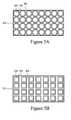
- FIGS. 5A-5Eillustrate plan views of multiple LEDs 201 , their associated spacers 301 , and the reflective layer 401 . While the shape of the individual LEDs 201 may be any shape, FIG. 5A illustrates a preferred embodiment in which the LEDs 201 are circular. In this embodiment the circular LEDs 201 preferably have a diameter of between about 10 nm and about 5,000 nm, with a preferred diameter of about 250 nm. The individual LEDs 201 are also preferably arranged in a grid pattern, with a pitch of between about 10 nm and about 10 ⁇ m, with a preferred pitch of about 250 nm, although other layouts, such as a staggered layout, may alternatively be used.
- FIG. 5Billustrates another preferred embodiment in which the LEDs 201 are rectangular in shape.
- the LEDs 201are also preferably arranged in a grid pattern with the reflective layer 401 between the individual LEDs 201 .
- the rectangular LEDs 201also preferably have a length of between about 10 nm and about 5,000 nm, with a preferred length of about 10 ⁇ m, a width of between about 10 nm and about 5,000 nm, with a preferred width of about 250 nm, and a spacing between the LEDs 201 of between about 10 nm and about 5,000 nm, with a preferred spacing of about 250 nm.
- FIG. 5Cillustrates yet another preferred embodiment in which the LEDs 201 are elliptical in shape.
- the elliptical LEDs 201are preferably, but not necessarily, arranged in a grid pattern, with a preferred spacing between the LEDs 201 of between about 10 nm and about 10 ⁇ m, with a preferred spacing of about 250 nm.
- FIG. 5Dillustrates yet another preferred embodiment in which the LEDs 201 are triangular in shape.
- the triangular LEDs 201are preferably arranged in rows and columns, although the LEDs 201 could alternatively be staggered.
- the LEDs 201 in this embodimentpreferably have a pitch of between about 10 nm and about 10 ⁇ m, with a preferred pitch of about 250 nm, and the triangular LEDs 201 preferably have a side length of between about 10 nm and about 5,000 nm, with a preferred side length of about 250 nm.
- FIG. 5Eillustrates yet another preferred embodiment in which the LEDs 201 are hexagonal in shape.
- the hexagonal LEDs 201are preferably arranged in rows and columns, although the LEDs 201 may alternatively be staggered so as not to align with each other.
- the LEDs 201preferably have a pitch of between about 10 nm and about 10 ⁇ m, with a preferred pitch of about 250 nm.
- FIG. 6illustrates the filling of the area above the reflective layer 401 and between the LEDs 201 with a fill material 601 and the formation of a top electrode 603 .
- the fill material 601preferably comprises a material that is transparent to LED radiation (e.g., visible light), such as silicon dioxide, and is preferably formed by, for example, chemical vapor deposition (CVD) techniques using tetra-ethyl-ortho-silicate (TEOS) and oxygen as precursors.
- CVDchemical vapor deposition
- TEOStetra-ethyl-ortho-silicate
- other materialssuch as silicon nitride, silicon oxynitride, or the like, and other processes, such as plasma enhanced CVD, may alternatively be used.
- the fill material 601is formed so as to overfill the areas between the LEDs 201 and above the reflective layer 401 .
- Excess fill material 601is then removed through a grinding process, such as chemical mechanical polishing (CMP), so as to expose the second contact layer 107 .
- CMPchemical mechanical polishing
- Other removal processessuch as etching or a combination of etching and grinding, may alternatively be used to remove the excess fill material 601 .
- a top electrode 603is formed in electrical contact with the second contact layer 107 of one or more of the LEDs 201 .
- the top electrode 603is preferably formed of a transparent, conductive material such as a thin layer of nickel, a thin layer of gold, a transparent conductive oxide, combinations of these, or the like, and may be formed through a process such as PVD, sputtering, CVD, or the like.
- the top electrode 603preferably has a thickness of between about 10 ⁇ and about 1,000 ⁇ , with a preferred thickness of about 100 ⁇ .
- processesmay be performed to complete the LEDs 201 .
- electrical contactsmay be formed to the first contact layer 103 in each LED 201 , either through a conductive substrate 101 or else through the formation of another contact in cases when the substrate is non-conductive.
- the LED devicemay be diced and packaged.
- a buffer layermay also be desirable between the first contact layer 103 and the substrate 101 .
- a buffer layersuch as AlN or AlGaN, may be desirable to aid in the epitaxial growth of a group III-N compound on the SiC substrate.
- a distributed Bragg reflectorgenerally comprises multiple layers having different refractive indices that cause light emitted from the LEDs to be reflected, thereby increasing the light emitted from the top of the LEDs 201 .
- a reflective buffer layermay also be used with or in place of the distributed Bragg reflector.
- the structure of the LEDs 201may also vary depending on the type of materials used and the intended application. It is expected that many types of LED structures may be used with embodiments of the present invention, which provides a reflective surface between the LEDs 201 .
- buffer layers or distributed Bragg reflectorsmay be used in conjunction with the LEDs.
- various materials and processesmay be varied while remaining within the scope of the present invention.
Landscapes
- Led Devices (AREA)
Abstract
Description
Claims (20)
Priority Applications (5)
| Application Number | Priority Date | Filing Date | Title |
|---|---|---|---|
| US12/270,309US8716723B2 (en) | 2008-08-18 | 2008-11-13 | Reflective layer between light-emitting diodes |
| TW098107980ATWI482262B (en) | 2008-08-18 | 2009-03-12 | Light emitting device and method of manufacturing same |
| US14/267,964US9214613B2 (en) | 2008-08-18 | 2014-05-02 | Method of forming light-generating device including reflective layer |
| US14/927,131US9698325B2 (en) | 2008-08-18 | 2015-10-29 | Light-emitting device including reflective layer |
| US15/613,628US10062821B2 (en) | 2008-08-18 | 2017-06-05 | Light-emitting device |
Applications Claiming Priority (2)
| Application Number | Priority Date | Filing Date | Title |
|---|---|---|---|
| US8975508P | 2008-08-18 | 2008-08-18 | |
| US12/270,309US8716723B2 (en) | 2008-08-18 | 2008-11-13 | Reflective layer between light-emitting diodes |
Related Child Applications (1)
| Application Number | Title | Priority Date | Filing Date |
|---|---|---|---|
| US14/267,964DivisionUS9214613B2 (en) | 2008-08-18 | 2014-05-02 | Method of forming light-generating device including reflective layer |
Publications (2)
| Publication Number | Publication Date |
|---|---|
| US20100038655A1 US20100038655A1 (en) | 2010-02-18 |
| US8716723B2true US8716723B2 (en) | 2014-05-06 |
Family
ID=41680681
Family Applications (8)
| Application Number | Title | Priority Date | Filing Date |
|---|---|---|---|
| US12/270,309Active2029-08-12US8716723B2 (en) | 2008-08-18 | 2008-11-13 | Reflective layer between light-emitting diodes |
| US14/267,964ActiveUS9214613B2 (en) | 2008-08-18 | 2014-05-02 | Method of forming light-generating device including reflective layer |
| US14/927,131ActiveUS9698325B2 (en) | 2008-08-18 | 2015-10-29 | Light-emitting device including reflective layer |
| US15/049,917ActiveUS9530948B2 (en) | 2008-08-18 | 2016-02-22 | Light emitting device having multi-layered electrode structure |
| US15/357,334ActiveUS9893257B2 (en) | 2008-08-18 | 2016-11-21 | Electrode structure of light emitting device |
| US15/613,628ActiveUS10062821B2 (en) | 2008-08-18 | 2017-06-05 | Light-emitting device |
| US15/854,462ActiveUS10038129B2 (en) | 2008-08-18 | 2017-12-26 | Light emitting device |
| US16/019,136ActiveUS10411177B2 (en) | 2008-08-18 | 2018-06-26 | Light emitting device |
Family Applications After (7)
| Application Number | Title | Priority Date | Filing Date |
|---|---|---|---|
| US14/267,964ActiveUS9214613B2 (en) | 2008-08-18 | 2014-05-02 | Method of forming light-generating device including reflective layer |
| US14/927,131ActiveUS9698325B2 (en) | 2008-08-18 | 2015-10-29 | Light-emitting device including reflective layer |
| US15/049,917ActiveUS9530948B2 (en) | 2008-08-18 | 2016-02-22 | Light emitting device having multi-layered electrode structure |
| US15/357,334ActiveUS9893257B2 (en) | 2008-08-18 | 2016-11-21 | Electrode structure of light emitting device |
| US15/613,628ActiveUS10062821B2 (en) | 2008-08-18 | 2017-06-05 | Light-emitting device |
| US15/854,462ActiveUS10038129B2 (en) | 2008-08-18 | 2017-12-26 | Light emitting device |
| US16/019,136ActiveUS10411177B2 (en) | 2008-08-18 | 2018-06-26 | Light emitting device |
Country Status (3)
| Country | Link |
|---|---|
| US (8) | US8716723B2 (en) |
| CN (1) | CN101655191A (en) |
| TW (1) | TWI482262B (en) |
Cited By (2)
| Publication number | Priority date | Publication date | Assignee | Title |
|---|---|---|---|---|
| US20160240518A1 (en)* | 2015-02-13 | 2016-08-18 | Nichia Corporation | Light emitting device |
| US11075192B2 (en)* | 2015-10-22 | 2021-07-27 | Commissariat A L'energie Atomique Et Aux Energies Alternatives | Microelectronic diode with optimised active surface |
Families Citing this family (37)
| Publication number | Priority date | Publication date | Assignee | Title |
|---|---|---|---|---|
| US8716723B2 (en)* | 2008-08-18 | 2014-05-06 | Tsmc Solid State Lighting Ltd. | Reflective layer between light-emitting diodes |
| US9293656B2 (en)* | 2012-11-02 | 2016-03-22 | Epistar Corporation | Light emitting device |
| KR101015845B1 (en)* | 2009-02-06 | 2011-02-23 | 삼성모바일디스플레이주식회사 | Organic electroluminescent display |
| KR101601624B1 (en)* | 2010-02-19 | 2016-03-09 | 삼성전자주식회사 | Semiconductor light emitting device having a multi-cell array, light emitting module and illumination apparatus |
| KR101047778B1 (en)* | 2010-04-01 | 2011-07-07 | 엘지이노텍 주식회사 | Light emitting device package and light unit having same |
| CN103069584A (en)* | 2010-08-11 | 2013-04-24 | 首尔Opto仪器股份有限公司 | UV light emitting diode and its manufacturing method |
| CN103155189B (en) | 2010-10-12 | 2017-02-22 | 皇家飞利浦电子股份有限公司 | Highly reflective coating on LED submount |
| US8664681B2 (en) | 2012-07-06 | 2014-03-04 | Invensas Corporation | Parallel plate slot emission array |
| US8816383B2 (en) | 2012-07-06 | 2014-08-26 | Invensas Corporation | High performance light emitting diode with vias |
| US9444015B2 (en) | 2014-06-18 | 2016-09-13 | X-Celeprint Limited | Micro assembled LED displays and lighting elements |
| US9991163B2 (en) | 2014-09-25 | 2018-06-05 | X-Celeprint Limited | Small-aperture-ratio display with electrical component |
| US9799719B2 (en) | 2014-09-25 | 2017-10-24 | X-Celeprint Limited | Active-matrix touchscreen |
| US9871345B2 (en) | 2015-06-09 | 2018-01-16 | X-Celeprint Limited | Crystalline color-conversion device |
| US10133426B2 (en) | 2015-06-18 | 2018-11-20 | X-Celeprint Limited | Display with micro-LED front light |
| US11061276B2 (en)* | 2015-06-18 | 2021-07-13 | X Display Company Technology Limited | Laser array display |
| US10380930B2 (en) | 2015-08-24 | 2019-08-13 | X-Celeprint Limited | Heterogeneous light emitter display system |
| US10230048B2 (en) | 2015-09-29 | 2019-03-12 | X-Celeprint Limited | OLEDs for micro transfer printing |
| US10066819B2 (en) | 2015-12-09 | 2018-09-04 | X-Celeprint Limited | Micro-light-emitting diode backlight system |
| US10193025B2 (en) | 2016-02-29 | 2019-01-29 | X-Celeprint Limited | Inorganic LED pixel structure |
| US10153256B2 (en) | 2016-03-03 | 2018-12-11 | X-Celeprint Limited | Micro-transfer printable electronic component |
| US10153257B2 (en) | 2016-03-03 | 2018-12-11 | X-Celeprint Limited | Micro-printed display |
| US10008483B2 (en) | 2016-04-05 | 2018-06-26 | X-Celeprint Limited | Micro-transfer printed LED and color filter structure |
| US10199546B2 (en) | 2016-04-05 | 2019-02-05 | X-Celeprint Limited | Color-filter device |
| US11137641B2 (en) | 2016-06-10 | 2021-10-05 | X Display Company Technology Limited | LED structure with polarized light emission |
| US9980341B2 (en) | 2016-09-22 | 2018-05-22 | X-Celeprint Limited | Multi-LED components |
| US10782002B2 (en) | 2016-10-28 | 2020-09-22 | X Display Company Technology Limited | LED optical components |
| US10347168B2 (en) | 2016-11-10 | 2019-07-09 | X-Celeprint Limited | Spatially dithered high-resolution |
| DE102016123013A1 (en)* | 2016-11-29 | 2018-05-30 | Osram Opto Semiconductors Gmbh | Display device with a plurality of separately operable pixels |
| JP6984168B2 (en)* | 2017-05-17 | 2021-12-17 | セイコーエプソン株式会社 | Imaging equipment and endoscope |
| CN109755266B (en)* | 2017-11-02 | 2021-01-12 | 錼创显示科技股份有限公司 | Micro light-emitting diode display panel |
| CN110504346B (en)* | 2018-05-16 | 2021-06-25 | 鸿富锦精密工业(深圳)有限公司 | Micro LED display panel manufacturing method and display panel |
| US11282984B2 (en)* | 2018-10-05 | 2022-03-22 | Seoul Viosys Co., Ltd. | Light emitting device |
| CN109659415A (en)* | 2018-12-28 | 2019-04-19 | 映瑞光电科技(上海)有限公司 | A kind of vertical LED chip and preparation method thereof |
| FR3111235A1 (en)* | 2020-06-04 | 2021-12-10 | Aledia | Optoelectronic device for light display with conductive light containment walls and method of manufacturing |
| KR20220031781A (en) | 2020-09-03 | 2022-03-14 | 삼성디스플레이 주식회사 | Display device and method for fabricating the same |
| US12379532B2 (en)* | 2021-05-07 | 2025-08-05 | Flightsafety International Inc. | Lightweight rigid mirror and a method of producing a lightweight rigid mirror |
| KR20230033218A (en)* | 2021-08-30 | 2023-03-08 | 삼성디스플레이 주식회사 | Light emitting element, display device including the same, and method of fabricating light emitting element |
Citations (46)
| Publication number | Priority date | Publication date | Assignee | Title |
|---|---|---|---|---|
| US4317086A (en)* | 1979-09-13 | 1982-02-23 | Xerox Corporation | Passivation and reflector structure for electroluminescent devices |
| US4984034A (en)* | 1981-02-09 | 1991-01-08 | Semiconductor Energy Laboratory Co., Ltd. | Non-single-crystalline light emitting semiconductor device matrix with insulation |
| US5803579A (en)* | 1996-06-13 | 1998-09-08 | Gentex Corporation | Illuminator assembly incorporating light emitting diodes |
| US5841128A (en)* | 1996-06-26 | 1998-11-24 | Oki Electric Industry Co., Ltd. | Optical sensor for reading a pattern |
| US5930279A (en)* | 1996-04-23 | 1999-07-27 | Compagnie Industrielle Des Lasers Cilas | Diode laser device arranged in the form of semiconductor arrays |
| US6410940B1 (en) | 2000-06-15 | 2002-06-25 | Kansas State University Research Foundation | Micro-size LED and detector arrays for minidisplay, hyper-bright light emitting diodes, lighting, and UV detector and imaging sensor applications |
| US20030087467A1 (en)* | 2001-07-11 | 2003-05-08 | Toyoharu Oohata | Semiconductor light emitting device, image display unit, lighting apparatus, and method of fabricating semiconductor light emitting device |
| US6635901B2 (en)* | 2000-12-15 | 2003-10-21 | Nobuhiko Sawaki | Semiconductor device including an InGaAIN layer |
| DE10220333A1 (en) | 2002-05-07 | 2003-11-27 | Osram Opto Semiconductors Gmbh | Radiation emitting semiconductor component for LED chips using microstructure elements with an active layer between two reflecting surfaces |
| US20040213017A1 (en)* | 2003-04-22 | 2004-10-28 | Shen-Hong Chou | [light source of back light module] |
| US20040238834A1 (en)* | 2003-05-30 | 2004-12-02 | Tsuyoshi Yasuoka | LED display apparatus |
| US20050023550A1 (en)* | 2003-07-29 | 2005-02-03 | Gelcore, Llc | Flip chip light emitting diode devices having thinned or removed substrates |
| US20050179044A1 (en)* | 2001-05-15 | 2005-08-18 | Toyoharu Oohata | Method for producing a display unit |
| US20050194598A1 (en) | 2004-02-13 | 2005-09-08 | Hwa-Mok Kim | Super bright light emitting diode of nanorod array structure having InGaN quantum well and method for manufacturing the same |
| US20050254243A1 (en)* | 2002-10-24 | 2005-11-17 | Hongxing Jiang | Light emitting diodes for high AC voltage operation and general lighting |
| US20060091408A1 (en) | 2004-10-29 | 2006-05-04 | Samsung Electro-Mechanics Co., Ltd. | Nitride based semiconductor device using nanorods and process for preparing the same |
| US20060102912A1 (en)* | 2004-11-16 | 2006-05-18 | Kyocera Corporation | Light emitting device |
| US20060175621A1 (en)* | 2001-12-28 | 2006-08-10 | Sanken Electric Co., Ltd. | Semiconductor light-emitting device light-emitting display method for manufacturing semiconductor light-emitting device and method for manufacturing light-emitting display |
| US20060180818A1 (en)* | 2003-07-30 | 2006-08-17 | Hideo Nagai | Semiconductor light emitting device, light emitting module and lighting apparatus |
| US20060214173A1 (en)* | 2005-03-28 | 2006-09-28 | Goldeneye, Inc. | Light emitting diodes and methods of fabrication |
| US7135711B2 (en)* | 2001-08-30 | 2006-11-14 | Osram Opto Semiconductors Gmbh | Electroluminescent body |
| US20070176188A1 (en)* | 2005-12-01 | 2007-08-02 | Shinichi Tanaka | Semiconductor light emitting device and its manufacture method |
| US20070190676A1 (en)* | 2005-01-11 | 2007-08-16 | Chen-Fu Chu | Light emitting diodes (leds) with improved light extraction by roughening |
| US20070215878A1 (en)* | 2006-03-17 | 2007-09-20 | Dong-Sing Wuu | Light emitting device |
| US20070262323A1 (en)* | 2006-05-10 | 2007-11-15 | Rohm Co., Ltd. | Semiconductor light emitting element array illuminator using the same |
| US20070278502A1 (en)* | 2004-09-13 | 2007-12-06 | Rohm Co., Ltd. | Semiconductor Light Emitting Device |
| US20080145961A1 (en)* | 2004-06-18 | 2008-06-19 | Naochika Horio | Semiconductor Light Emitting Device and Manufacturing Method Thereof |
| US20080142814A1 (en)* | 2005-01-11 | 2008-06-19 | Chen-Fu Chu | Light emitting diodes (leds) with improved light extraction by roughening |
| US20080149945A1 (en)* | 2003-08-28 | 2008-06-26 | Hideo Nagai | Semiconductor light emitting device, light emitting module, lighting apparatus, display element and manufacturing method of semiconductor light emitting device |
| US20080149946A1 (en)* | 2006-12-22 | 2008-06-26 | Philips Lumileds Lighting Company, Llc | Semiconductor Light Emitting Device Configured To Emit Multiple Wavelengths Of Light |
| US20080237622A1 (en)* | 2007-03-29 | 2008-10-02 | Samsung Electro-Mechanics Co., Ltd. | Light emitting device and package having the same |
| US20080251796A1 (en)* | 2005-06-22 | 2008-10-16 | Seoul Opto-Device Co., Ltd. | Light Emitting Device and Method of Manufacturing the Same |
| US20080251808A1 (en)* | 2002-08-01 | 2008-10-16 | Takeshi Kususe | Semiconductor light-emitting device, method for manufacturing the same, and light-emitting apparatus including the same |
| US20080258156A1 (en)* | 2006-09-29 | 2008-10-23 | Sanyo Electric Co., Ltd. | Light-emitting diode apparatus |
| US20090085048A1 (en)* | 2007-09-27 | 2009-04-02 | Seoul Opto Device Co., Ltd. | Ac light emitting diode |
| US20090121241A1 (en)* | 2007-11-14 | 2009-05-14 | Cree, Inc. | Wire bond free wafer level LED |
| US20090212318A1 (en)* | 2002-04-17 | 2009-08-27 | Sharp Kabushiki Kaisha | Nitride-based semiconductor light-emitting device and manufacturing method thereof |
| US20090242910A1 (en)* | 2008-03-28 | 2009-10-01 | Sanken Electric Co., Ltd. | Light emitting device |
| US20090267085A1 (en)* | 2005-03-11 | 2009-10-29 | Seoul Semiconductor Co., Ltd. | Led package having an array of light emitting cells coupled in series |
| US20100032696A1 (en)* | 2008-08-11 | 2010-02-11 | Chen-Hua Yu | Light-Emitting Diode with Textured Substrate |
| US7719013B2 (en)* | 2004-12-02 | 2010-05-18 | Samsung Electro-Mechanics Co., Ltd. | Semiconductor light emitting device and method of manufacturing the same |
| US7834370B2 (en)* | 2004-11-25 | 2010-11-16 | Panasonic Corporation | Semiconductor light emitting device, illuminating device, mobile communication device, camera, and manufacturing method therefor |
| US8022419B2 (en)* | 2005-12-19 | 2011-09-20 | Showa Denko K.K. | Flip-chip type semiconductor light-emitting device, method for manufacturing flip-chip type semiconductor light-emitting device, printed circuit board for flip-chip type semiconductor light-emitting device, mounting structure for flip-chip type semiconductor light-emitting device, and light-emitting diode lamp |
| US8058663B2 (en)* | 2007-09-26 | 2011-11-15 | Iii-N Technology, Inc. | Micro-emitter array based full-color micro-display |
| US20110284903A1 (en)* | 2007-04-18 | 2011-11-24 | Loh Ban P | Semiconductor Light Emitting Device Packages and Methods |
| US8272757B1 (en)* | 2005-06-03 | 2012-09-25 | Ac Led Lighting, L.L.C. | Light emitting diode lamp capable of high AC/DC voltage operation |
Family Cites Families (47)
| Publication number | Priority date | Publication date | Assignee | Title |
|---|---|---|---|---|
| US2005101A (en) | 1934-09-26 | 1935-06-18 | Herberts Machinery Co Ltd | Lathe |
| US2009900A (en) | 1935-01-08 | 1935-07-30 | Draper Corp | Filling stop motion |
| JP4024994B2 (en) | 2000-06-30 | 2007-12-19 | 株式会社東芝 | Semiconductor light emitting device |
| US6958498B2 (en) | 2002-09-27 | 2005-10-25 | Emcore Corporation | Optimized contact design for flip-chip LED |
| AU2003280878A1 (en) | 2002-11-16 | 2004-06-15 | Lg Innotek Co., Ltd | Light emitting device and fabrication method thereof |
| JP2005277374A (en) | 2004-02-26 | 2005-10-06 | Toyoda Gosei Co Ltd | Group III nitride compound semiconductor light emitting device and method of manufacturing the same |
| US8115212B2 (en) | 2004-07-29 | 2012-02-14 | Showa Denko K.K. | Positive electrode for semiconductor light-emitting device |
| CN100590898C (en) | 2004-07-29 | 2010-02-17 | 昭和电工株式会社 | Positive electrode for semiconductor light emitting devices |
| JP4579654B2 (en) | 2004-11-11 | 2010-11-10 | パナソニック株式会社 | SEMICONDUCTOR LIGHT EMITTING DEVICE AND ITS MANUFACTURING METHOD, AND LIGHTING MODULE AND LIGHTING DEVICE HAVING SEMICONDUCTOR LIGHT EMITTING DEVICE |
| WO2007091704A1 (en)* | 2006-02-08 | 2007-08-16 | Showa Denko K.K. | Light-emitting diode and fabrication method thereof |
| JP5162909B2 (en) | 2006-04-03 | 2013-03-13 | 豊田合成株式会社 | Semiconductor light emitting device |
| JP5056082B2 (en) | 2006-04-17 | 2012-10-24 | 日亜化学工業株式会社 | Semiconductor light emitting device |
| JP4656525B2 (en) | 2006-04-24 | 2011-03-23 | 株式会社沖データ | Semiconductor device, LED head, and image forming apparatus |
| JP5126875B2 (en) | 2006-08-11 | 2013-01-23 | シャープ株式会社 | Manufacturing method of nitride semiconductor light emitting device |
| KR100836494B1 (en)* | 2006-12-26 | 2008-06-09 | 엘지이노텍 주식회사 | Semiconductor light emitting device |
| TWI331411B (en) | 2006-12-29 | 2010-10-01 | Epistar Corp | High efficiency light-emitting diode and method for manufacturing the same |
| WO2009113659A1 (en) | 2008-03-13 | 2009-09-17 | 昭和電工株式会社 | Semiconductor light-emitting device and method for manufacturing the same |
| JP2009283551A (en) | 2008-05-20 | 2009-12-03 | Showa Denko Kk | Semiconductor light emitting element, method for manufacturing thereof, and lamp |
| CN104538507B (en)* | 2008-06-02 | 2017-08-15 | Lg伊诺特有限公司 | Method for preparing semiconductor light-emitting apparatus |
| CN102124574B (en) | 2008-06-16 | 2013-07-17 | 丰田合成株式会社 | Semiconductor light emitting element, electrode and manufacturing method for the element, and lamp |
| KR20100008123A (en)* | 2008-07-15 | 2010-01-25 | 고려대학교 산학협력단 | Vertical light emitting devices with the support composed of double heat-sinking layer |
| US8633501B2 (en) | 2008-08-12 | 2014-01-21 | Epistar Corporation | Light-emitting device having a patterned surface |
| US9293656B2 (en)* | 2012-11-02 | 2016-03-22 | Epistar Corporation | Light emitting device |
| US8716723B2 (en)* | 2008-08-18 | 2014-05-06 | Tsmc Solid State Lighting Ltd. | Reflective layer between light-emitting diodes |
| JP5376866B2 (en)* | 2008-08-22 | 2013-12-25 | スタンレー電気株式会社 | Semiconductor light emitting device manufacturing method and semiconductor light emitting device |
| US8815618B2 (en)* | 2008-08-29 | 2014-08-26 | Tsmc Solid State Lighting Ltd. | Light-emitting diode on a conductive substrate |
| JP2010067890A (en)* | 2008-09-12 | 2010-03-25 | Hitachi Cable Ltd | Light-emitting element |
| JP5232972B2 (en)* | 2008-10-20 | 2013-07-10 | 豊田合成株式会社 | Semiconductor light emitting device and method for manufacturing semiconductor light emitting device |
| US8896085B2 (en) | 2009-07-10 | 2014-11-25 | Toyoda Gosei Co., Ltd. | Semiconductor light-emitting element manufacturing method, lamp, electronic equipment, and mechanical apparatus |
| WO2011018942A1 (en)* | 2009-08-13 | 2011-02-17 | 昭和電工株式会社 | Semiconductor light-emitting element, semiconductor light-emitting device, method for producing semiconductor light-emitting element, method for producing semiconductor light-emitting device, illumination device using semiconductor light-emitting device, and electronic apparatus |
| US8552455B2 (en) | 2009-09-07 | 2013-10-08 | Seoul Opto Device Co., Ltd. | Semiconductor light-emitting diode and a production method therefor |
| CN102630349B (en) | 2009-09-18 | 2017-06-13 | 天空公司 | Power light emitting diode and method of operating with current density |
| JP5497417B2 (en) | 2009-12-10 | 2014-05-21 | 富士フイルム株式会社 | THIN FILM TRANSISTOR, MANUFACTURING METHOD THEREOF, AND APPARATUS HAVING THE THIN FILM TRANSISTOR |
| US8637888B2 (en)* | 2009-12-11 | 2014-01-28 | Toyoda Gosei Co., Ltd. | Semiconductor light emitting element, light emitting device using semiconductor light emitting element, and electronic apparatus |
| US8154042B2 (en) | 2010-04-29 | 2012-04-10 | Koninklijke Philips Electronics N V | Light emitting device with trenches and a top contact |
| TWI466325B (en)* | 2010-06-25 | 2014-12-21 | Toyoda Gosei Kk | Semiconductor light emitting element |
| JP5582054B2 (en) | 2011-02-09 | 2014-09-03 | 豊田合成株式会社 | Semiconductor light emitting device |
| KR20120134456A (en) | 2011-06-02 | 2012-12-12 | 엘지이노텍 주식회사 | Light emitting element |
| US8860059B2 (en)* | 2011-06-20 | 2014-10-14 | Xiamen Sanan Optoelectronics Technology Co., Ltd. | Light emitting devices, systems, and methods of manufacturing |
| JP6077201B2 (en)* | 2011-08-11 | 2017-02-08 | 昭和電工株式会社 | Light emitting diode and manufacturing method thereof |
| US9070613B2 (en) | 2011-09-07 | 2015-06-30 | Lg Innotek Co., Ltd. | Light emitting device |
| KR101872735B1 (en) | 2011-11-15 | 2018-08-02 | 엘지이노텍 주식회사 | Light emitting device package |
| KR101969334B1 (en)* | 2011-11-16 | 2019-04-17 | 엘지이노텍 주식회사 | Light emitting device and light emitting apparatus having the same |
| TWI458122B (en)* | 2011-11-23 | 2014-10-21 | Toshiba Kk | Semiconductor light-emitting element |
| CN102637681B (en)* | 2012-04-28 | 2014-07-30 | 厦门市三安光电科技有限公司 | Vertical light-emitting device and manufacturing method thereof |
| US9437783B2 (en) | 2012-05-08 | 2016-09-06 | Cree, Inc. | Light emitting diode (LED) contact structures and process for fabricating the same |
| JP2014007252A (en)* | 2012-06-22 | 2014-01-16 | Stanley Electric Co Ltd | Semiconductor light-emitting element and semiconductor light-emitting element manufacturing method |
- 2008
- 2008-11-13USUS12/270,309patent/US8716723B2/enactiveActive
- 2009
- 2009-03-12TWTW098107980Apatent/TWI482262B/enactive
- 2009-05-05CNCN200910139105Apatent/CN101655191A/enactivePending
- 2014
- 2014-05-02USUS14/267,964patent/US9214613B2/enactiveActive
- 2015
- 2015-10-29USUS14/927,131patent/US9698325B2/enactiveActive
- 2016
- 2016-02-22USUS15/049,917patent/US9530948B2/enactiveActive
- 2016-11-21USUS15/357,334patent/US9893257B2/enactiveActive
- 2017
- 2017-06-05USUS15/613,628patent/US10062821B2/enactiveActive
- 2017-12-26USUS15/854,462patent/US10038129B2/enactiveActive
- 2018
- 2018-06-26USUS16/019,136patent/US10411177B2/enactiveActive
Patent Citations (48)
| Publication number | Priority date | Publication date | Assignee | Title |
|---|---|---|---|---|
| US4317086A (en)* | 1979-09-13 | 1982-02-23 | Xerox Corporation | Passivation and reflector structure for electroluminescent devices |
| US4984034A (en)* | 1981-02-09 | 1991-01-08 | Semiconductor Energy Laboratory Co., Ltd. | Non-single-crystalline light emitting semiconductor device matrix with insulation |
| US5930279A (en)* | 1996-04-23 | 1999-07-27 | Compagnie Industrielle Des Lasers Cilas | Diode laser device arranged in the form of semiconductor arrays |
| US5803579A (en)* | 1996-06-13 | 1998-09-08 | Gentex Corporation | Illuminator assembly incorporating light emitting diodes |
| US5841128A (en)* | 1996-06-26 | 1998-11-24 | Oki Electric Industry Co., Ltd. | Optical sensor for reading a pattern |
| US6410940B1 (en) | 2000-06-15 | 2002-06-25 | Kansas State University Research Foundation | Micro-size LED and detector arrays for minidisplay, hyper-bright light emitting diodes, lighting, and UV detector and imaging sensor applications |
| US6635901B2 (en)* | 2000-12-15 | 2003-10-21 | Nobuhiko Sawaki | Semiconductor device including an InGaAIN layer |
| US20050179044A1 (en)* | 2001-05-15 | 2005-08-18 | Toyoharu Oohata | Method for producing a display unit |
| US20030087467A1 (en)* | 2001-07-11 | 2003-05-08 | Toyoharu Oohata | Semiconductor light emitting device, image display unit, lighting apparatus, and method of fabricating semiconductor light emitting device |
| US7135711B2 (en)* | 2001-08-30 | 2006-11-14 | Osram Opto Semiconductors Gmbh | Electroluminescent body |
| US20060175621A1 (en)* | 2001-12-28 | 2006-08-10 | Sanken Electric Co., Ltd. | Semiconductor light-emitting device light-emitting display method for manufacturing semiconductor light-emitting device and method for manufacturing light-emitting display |
| US20090212318A1 (en)* | 2002-04-17 | 2009-08-27 | Sharp Kabushiki Kaisha | Nitride-based semiconductor light-emitting device and manufacturing method thereof |
| DE10220333A1 (en) | 2002-05-07 | 2003-11-27 | Osram Opto Semiconductors Gmbh | Radiation emitting semiconductor component for LED chips using microstructure elements with an active layer between two reflecting surfaces |
| US20080251808A1 (en)* | 2002-08-01 | 2008-10-16 | Takeshi Kususe | Semiconductor light-emitting device, method for manufacturing the same, and light-emitting apparatus including the same |
| US20050254243A1 (en)* | 2002-10-24 | 2005-11-17 | Hongxing Jiang | Light emitting diodes for high AC voltage operation and general lighting |
| US20040213017A1 (en)* | 2003-04-22 | 2004-10-28 | Shen-Hong Chou | [light source of back light module] |
| US20040238834A1 (en)* | 2003-05-30 | 2004-12-02 | Tsuyoshi Yasuoka | LED display apparatus |
| US20050023550A1 (en)* | 2003-07-29 | 2005-02-03 | Gelcore, Llc | Flip chip light emitting diode devices having thinned or removed substrates |
| US20060180818A1 (en)* | 2003-07-30 | 2006-08-17 | Hideo Nagai | Semiconductor light emitting device, light emitting module and lighting apparatus |
| US20080149945A1 (en)* | 2003-08-28 | 2008-06-26 | Hideo Nagai | Semiconductor light emitting device, light emitting module, lighting apparatus, display element and manufacturing method of semiconductor light emitting device |
| US20050194598A1 (en) | 2004-02-13 | 2005-09-08 | Hwa-Mok Kim | Super bright light emitting diode of nanorod array structure having InGaN quantum well and method for manufacturing the same |
| US20080145961A1 (en)* | 2004-06-18 | 2008-06-19 | Naochika Horio | Semiconductor Light Emitting Device and Manufacturing Method Thereof |
| US20070278502A1 (en)* | 2004-09-13 | 2007-12-06 | Rohm Co., Ltd. | Semiconductor Light Emitting Device |
| US20060091408A1 (en) | 2004-10-29 | 2006-05-04 | Samsung Electro-Mechanics Co., Ltd. | Nitride based semiconductor device using nanorods and process for preparing the same |
| US20060102912A1 (en)* | 2004-11-16 | 2006-05-18 | Kyocera Corporation | Light emitting device |
| US7834370B2 (en)* | 2004-11-25 | 2010-11-16 | Panasonic Corporation | Semiconductor light emitting device, illuminating device, mobile communication device, camera, and manufacturing method therefor |
| US7719013B2 (en)* | 2004-12-02 | 2010-05-18 | Samsung Electro-Mechanics Co., Ltd. | Semiconductor light emitting device and method of manufacturing the same |
| US20080142814A1 (en)* | 2005-01-11 | 2008-06-19 | Chen-Fu Chu | Light emitting diodes (leds) with improved light extraction by roughening |
| US20070190676A1 (en)* | 2005-01-11 | 2007-08-16 | Chen-Fu Chu | Light emitting diodes (leds) with improved light extraction by roughening |
| US20110140135A1 (en)* | 2005-03-11 | 2011-06-16 | Seoul Semiconductor Co., Ltd. | Led package having an array of light emitting cells coupled in series |
| US20090267085A1 (en)* | 2005-03-11 | 2009-10-29 | Seoul Semiconductor Co., Ltd. | Led package having an array of light emitting cells coupled in series |
| US20060214173A1 (en)* | 2005-03-28 | 2006-09-28 | Goldeneye, Inc. | Light emitting diodes and methods of fabrication |
| US8272757B1 (en)* | 2005-06-03 | 2012-09-25 | Ac Led Lighting, L.L.C. | Light emitting diode lamp capable of high AC/DC voltage operation |
| US20080251796A1 (en)* | 2005-06-22 | 2008-10-16 | Seoul Opto-Device Co., Ltd. | Light Emitting Device and Method of Manufacturing the Same |
| US20070176188A1 (en)* | 2005-12-01 | 2007-08-02 | Shinichi Tanaka | Semiconductor light emitting device and its manufacture method |
| US8022419B2 (en)* | 2005-12-19 | 2011-09-20 | Showa Denko K.K. | Flip-chip type semiconductor light-emitting device, method for manufacturing flip-chip type semiconductor light-emitting device, printed circuit board for flip-chip type semiconductor light-emitting device, mounting structure for flip-chip type semiconductor light-emitting device, and light-emitting diode lamp |
| US20070215878A1 (en)* | 2006-03-17 | 2007-09-20 | Dong-Sing Wuu | Light emitting device |
| US20070262323A1 (en)* | 2006-05-10 | 2007-11-15 | Rohm Co., Ltd. | Semiconductor light emitting element array illuminator using the same |
| US20080258156A1 (en)* | 2006-09-29 | 2008-10-23 | Sanyo Electric Co., Ltd. | Light-emitting diode apparatus |
| US20080149946A1 (en)* | 2006-12-22 | 2008-06-26 | Philips Lumileds Lighting Company, Llc | Semiconductor Light Emitting Device Configured To Emit Multiple Wavelengths Of Light |
| US20080237622A1 (en)* | 2007-03-29 | 2008-10-02 | Samsung Electro-Mechanics Co., Ltd. | Light emitting device and package having the same |
| US20110284903A1 (en)* | 2007-04-18 | 2011-11-24 | Loh Ban P | Semiconductor Light Emitting Device Packages and Methods |
| US8058663B2 (en)* | 2007-09-26 | 2011-11-15 | Iii-N Technology, Inc. | Micro-emitter array based full-color micro-display |
| US20090085048A1 (en)* | 2007-09-27 | 2009-04-02 | Seoul Opto Device Co., Ltd. | Ac light emitting diode |
| US20090121241A1 (en)* | 2007-11-14 | 2009-05-14 | Cree, Inc. | Wire bond free wafer level LED |
| US20090242910A1 (en)* | 2008-03-28 | 2009-10-01 | Sanken Electric Co., Ltd. | Light emitting device |
| US20100032696A1 (en)* | 2008-08-11 | 2010-02-11 | Chen-Hua Yu | Light-Emitting Diode with Textured Substrate |
| US8058082B2 (en)* | 2008-08-11 | 2011-11-15 | Taiwan Semiconductor Manufacturing Company, Ltd. | Light-emitting diode with textured substrate |
Non-Patent Citations (1)
| Title |
|---|
| Chinese Office Action, Aug. 9, 2010, 5 pages. |
Cited By (4)
| Publication number | Priority date | Publication date | Assignee | Title |
|---|---|---|---|---|
| US20160240518A1 (en)* | 2015-02-13 | 2016-08-18 | Nichia Corporation | Light emitting device |
| US10720412B2 (en)* | 2015-02-13 | 2020-07-21 | Nichia Corporation | Light emitting device |
| US11508701B2 (en) | 2015-02-13 | 2022-11-22 | Nichia Corporation | Light emitting device |
| US11075192B2 (en)* | 2015-10-22 | 2021-07-27 | Commissariat A L'energie Atomique Et Aux Energies Alternatives | Microelectronic diode with optimised active surface |
Also Published As
| Publication number | Publication date |
|---|---|
| US20180309038A1 (en) | 2018-10-25 |
| US9214613B2 (en) | 2015-12-15 |
| US9698325B2 (en) | 2017-07-04 |
| US20160064632A1 (en) | 2016-03-03 |
| US20180138380A1 (en) | 2018-05-17 |
| US20170069810A1 (en) | 2017-03-09 |
| US10038129B2 (en) | 2018-07-31 |
| US10411177B2 (en) | 2019-09-10 |
| US10062821B2 (en) | 2018-08-28 |
| US20140235001A1 (en) | 2014-08-21 |
| US20100038655A1 (en) | 2010-02-18 |
| US20160172557A1 (en) | 2016-06-16 |
| TW201010050A (en) | 2010-03-01 |
| US9530948B2 (en) | 2016-12-27 |
| TWI482262B (en) | 2015-04-21 |
| CN101655191A (en) | 2010-02-24 |
| US20170271568A1 (en) | 2017-09-21 |
| US9893257B2 (en) | 2018-02-13 |
Similar Documents
| Publication | Publication Date | Title |
|---|---|---|
| US10062821B2 (en) | Light-emitting device | |
| US8766309B2 (en) | Omnidirectional reflector | |
| US9130115B2 (en) | Light-emitting diode with textured substrate | |
| US9373755B2 (en) | Light-emitting diodes on concave texture substrate | |
| US9741897B2 (en) | Thin light emitting diode and fabrication method | |
| US8742441B2 (en) | Light-emitting diode with embedded elements | |
| WO2013039344A2 (en) | Light emitting diode and method of manufacturing same | |
| US10069037B2 (en) | Light-emitting device and manufacturing method thereof | |
| US20160104814A1 (en) | Vertical-type semiconductor light-emmitting device and method of fabricating the vertical-type light-emitting device | |
| KR20130025856A (en) | Nano rod light emitting device | |
| US9306120B2 (en) | High efficiency light emitting diode | |
| KR20060134490A (en) | Flip Chip Nitride Semiconductor Light Emitting Diode and Manufacturing Method Thereof | |
| TWI424589B (en) | Light-emitting diode device and method of forming same | |
| KR20110085727A (en) | Semiconductor light emitting device and method for manufacturing same | |
| KR20150109143A (en) | Light emitting device having buffer layer and method of fabricating the same |
Legal Events
| Date | Code | Title | Description |
|---|---|---|---|
| AS | Assignment | Owner name:TAIWAN SEMICONDUCTOR MANUFACTURING COMPANY, LTD.,T Free format text:ASSIGNMENT OF ASSIGNORS INTEREST;ASSIGNORS:CHEN, DING-YUAN;YU, CHIA-LIN;YU, CHEN-HUA;AND OTHERS;REEL/FRAME:021831/0556 Effective date:20081112 Owner name:TAIWAN SEMICONDUCTOR MANUFACTURING COMPANY, LTD., Free format text:ASSIGNMENT OF ASSIGNORS INTEREST;ASSIGNORS:CHEN, DING-YUAN;YU, CHIA-LIN;YU, CHEN-HUA;AND OTHERS;REEL/FRAME:021831/0556 Effective date:20081112 | |
| AS | Assignment | Owner name:TSMC SOLID STATE LIGHTING LTD., TAIWAN Free format text:ASSIGNMENT OF ASSIGNORS INTEREST;ASSIGNOR:TAIWAN SEMICONDUCTOR MANUFACTURING COMPANY LTD.;REEL/FRAME:027855/0937 Effective date:20120301 | |
| STCF | Information on status: patent grant | Free format text:PATENTED CASE | |
| AS | Assignment | Owner name:EPISTAR CORPORATION, TAIWAN Free format text:MERGER;ASSIGNOR:CHIP STAR LTD.;REEL/FRAME:037805/0571 Effective date:20150715 Owner name:CHIP STAR LTD., TAIWAN Free format text:CHANGE OF NAME;ASSIGNOR:TSMC SOLID STATE LIGHTING LTD.;REEL/FRAME:037809/0929 Effective date:20150402 | |
| MAFP | Maintenance fee payment | Free format text:PAYMENT OF MAINTENANCE FEE, 4TH YEAR, LARGE ENTITY (ORIGINAL EVENT CODE: M1551) Year of fee payment:4 | |
| MAFP | Maintenance fee payment | Free format text:PAYMENT OF MAINTENANCE FEE, 8TH YEAR, LARGE ENTITY (ORIGINAL EVENT CODE: M1552); ENTITY STATUS OF PATENT OWNER: LARGE ENTITY Year of fee payment:8 |