US8716094B1 - FinFET formation using double patterning memorization - Google Patents
FinFET formation using double patterning memorizationDownload PDFInfo
- Publication number
- US8716094B1 US8716094B1US13/682,769US201213682769AUS8716094B1US 8716094 B1US8716094 B1US 8716094B1US 201213682769 AUS201213682769 AUS 201213682769AUS 8716094 B1US8716094 B1US 8716094B1
- Authority
- US
- United States
- Prior art keywords
- lithography
- layer
- over
- gate
- etching
- Prior art date
- Legal status (The legal status is an assumption and is not a legal conclusion. Google has not performed a legal analysis and makes no representation as to the accuracy of the status listed.)
- Active
Links
- 238000000059patterningMethods0.000titleabstractdescription11
- 230000015572biosynthetic processEffects0.000titledescription4
- 238000000034methodMethods0.000claimsabstractdescription51
- 229910021420polycrystalline siliconInorganic materials0.000claimsabstractdescription27
- 230000008569processEffects0.000claimsabstractdescription22
- 238000000151depositionMethods0.000claimsabstractdescription15
- 238000005530etchingMethods0.000claimsdescription18
- XUIMIQQOPSSXEZ-UHFFFAOYSA-NSiliconChemical compound[Si]XUIMIQQOPSSXEZ-UHFFFAOYSA-N0.000claimsdescription17
- 238000001459lithographyMethods0.000claimsdescription17
- 229910052710siliconInorganic materials0.000claimsdescription17
- 239000010703siliconSubstances0.000claimsdescription17
- 150000004767nitridesChemical class0.000claimsdescription9
- 238000005498polishingMethods0.000claimsdescription6
- 229910052581Si3N4Inorganic materials0.000claimsdescription5
- 238000005229chemical vapour depositionMethods0.000claimsdescription5
- HQVNEWCFYHHQES-UHFFFAOYSA-Nsilicon nitrideChemical compoundN12[Si]34N5[Si]62N3[Si]51N64HQVNEWCFYHHQES-UHFFFAOYSA-N0.000claimsdescription5
- 239000000126substanceSubstances0.000claimsdescription3
- 230000001590oxidative effectEffects0.000claims3
- 238000013459approachMethods0.000abstractdescription8
- 239000004065semiconductorSubstances0.000description4
- 238000013461designMethods0.000description2
- 230000000694effectsEffects0.000description2
- 238000012986modificationMethods0.000description2
- 230000004048modificationEffects0.000description2
- 239000006117anti-reflective coatingSubstances0.000description1
- 238000003491arrayMethods0.000description1
- 239000011248coating agentSubstances0.000description1
- 238000000576coating methodMethods0.000description1
- 230000007547defectEffects0.000description1
- 230000008021depositionEffects0.000description1
- 230000005669field effectEffects0.000description1
- 230000008014freezingEffects0.000description1
- 238000007710freezingMethods0.000description1
- 230000006870functionEffects0.000description1
- 238000000671immersion lithographyMethods0.000description1
- 230000007246mechanismEffects0.000description1
- 229910044991metal oxideInorganic materials0.000description1
- 150000004706metal oxidesChemical class0.000description1
- 230000003287optical effectEffects0.000description1
- 230000003071parasitic effectEffects0.000description1
- 238000012545processingMethods0.000description1
- 238000012546transferMethods0.000description1
- 230000007704transitionEffects0.000description1
- 230000001960triggered effectEffects0.000description1
- 238000004148unit processMethods0.000description1
Images


Classifications
- H—ELECTRICITY
- H10—SEMICONDUCTOR DEVICES; ELECTRIC SOLID-STATE DEVICES NOT OTHERWISE PROVIDED FOR
- H10D—INORGANIC ELECTRIC SEMICONDUCTOR DEVICES
- H10D30/00—Field-effect transistors [FET]
- H10D30/01—Manufacture or treatment
- H10D30/021—Manufacture or treatment of FETs having insulated gates [IGFET]
- H10D30/031—Manufacture or treatment of FETs having insulated gates [IGFET] of thin-film transistors [TFT]
- H—ELECTRICITY
- H10—SEMICONDUCTOR DEVICES; ELECTRIC SOLID-STATE DEVICES NOT OTHERWISE PROVIDED FOR
- H10D—INORGANIC ELECTRIC SEMICONDUCTOR DEVICES
- H10D30/00—Field-effect transistors [FET]
- H10D30/01—Manufacture or treatment
- H10D30/021—Manufacture or treatment of FETs having insulated gates [IGFET]
- H10D30/024—Manufacture or treatment of FETs having insulated gates [IGFET] of fin field-effect transistors [FinFET]
Definitions
- This inventionrelates generally to the field of semiconductors and, more particularly, to approaches for fabricating fin-shaped field effect transistors (FinFETs) using double patterning memorization techniques.
- CMOScomplementary metal-oxide semiconductor
- 3Dthree-dimensional
- FinFETsoffer improved channel control and, therefore, reduced short channel effects.
- the gate in a planar transistorsits above the channel, the gate of a FinFET wraps around the channel, providing electrostatic control from both sides.
- the 3D structureintroduces new parasitic capacitances and new critical dimensions that must be controlled to optimize performance.
- gate length and pitchalso scale down.
- the device scalinghas reached an era that is below the practical limit of the current most advanced deep ultraviolet light (DUV) immersion lithography system for single patterning which necessitates multiple patterning schemes.
- DUVdeep ultraviolet light
- Lggate length
- L1first (L1) and the second (L2) patterns.
- the first (L1) patternhas higher critical dimension uniformity (CDU), line edge roughness/line width roughness (LER/LWR) values due to its inherent additional freezing process, while the second (L2) pattern has higher etch bias due to different etch resistance of the two resists.
- CDUcritical dimension uniformity
- LER/LWRline edge roughness/line width roughness
- LER/LWRline edge roughness/line width roughness
- L2second (L2) pattern has higher etch bias due to different etch resistance of the two resists.
- the chemical freeze processhas consistently been faced with defects and performance issues. As such, existing approaches fail to provide a consistent and reliable result.
- a devicewill initially be formed by defining a set of fins (e.g., over a buried oxide layer and a silicon layer), depositing a poly-silicon layer, and depositing a hardmask. Thereafter, a front end of the line (FEOL) lithography-etch, lithography-etch (LELE) process will be performed to form a set of trenches in the device. The set of trenches will be filled with an oxide layer that is subsequently polished. Thereafter, the device is selectively etched to yield a gate pattern (e.g., poly-silicon).
- FEOLfront end of the line
- LELElithography-etch
- a first aspect of the present inventionprovides a method for forming a FinFET device, comprising: defining a set of fins over a silicon layer; forming a poly-silicon layer over the set of fins; forming a hardmask layer over the poly-silicon layer; performing a lithography-etch, lithography-etch process to form a set of trenches over the hardmask layer; forming an oxide layer to fill the set of trenches; polishing the oxide layer; and selectively etching the FinFET device to yield a gate pattern.
- a second aspect of the present inventionprovides a method for forming a FinFET device, comprising: defining a set of fins over a silicon layer, the silicon layer being formed over a buried oxide layer; depositing a poly-silicon layer over the set of fins; depositing a hardmask layer over the poly-silicon layer; performing a lithography-etch, lithography-etch process to form a set of trenches over the hardmask layer; filling the set of trenches with an oxide layer; planarizing the oxide layer; and selectively etching the FinFET device to yield a gate pattern.
- a third aspect of the present inventionprovides a method for forming a FinFET device, comprising: depositing a poly-silicon layer over a set of fins, the set of fins being formed over a silicon layer; depositing a silicon nitride hardmask layer over the poly-silicon layer; performing a front end of the line (FEOL) lithography-etch, lithography-etch process to form a set of trenches over the hardmask layer; filling the set of trenches with an oxide layer; planarizing the oxide layer; and performing a selective nitride etching to yield a poly-silicon gate pattern in the device.
- FEOLfront end of the line
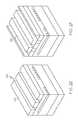
- FIGS. 1A-Bshow a progression of a FinFET device during its formation according to an embodiment of the present invention.
- FIGS. 2A-Jshow a progression of a FinFET device during its formation according to an embodiment of the present invention.
- first elementsuch as a first structure (e.g., a first layer) is present on a second element, such as a second structure (e.g. a second layer) wherein intervening elements, such as an interface structure (e.g. interface layer) may be present between the first element and the second element.
- first structuree.g., a first layer
- second structuree.g. a second layer
- intervening elementssuch as an interface structure (e.g. interface layer) may be present between the first element and the second element.
- a devicewill initially be formed by defining a set of fins (e.g., over a buried oxide layer and a silicon layer), depositing a poly-silicon layer, and depositing a hardmask. Thereafter, a front end of the line (FEOL) lithography-etch, lithography-etch (LELE) process will be performed to form a set of trenches in the device. The set of trenches will be filled with an oxide layer that is subsequently polished. Thereafter, the device is selectively etched to yield a gate pattern (e.g., poly-silicon).
- FEOLfront end of the line
- LELElithography-etch
- FIGS. 1A-BAn example of this is shown in FIGS. 1A-B .
- a silicon layer 12is formed over a buried oxide layer (BOX) 10 .
- a dummy poly-silicon layer 14is then deposited over the silicon layer 12 .
- a hardmask layerwill be deposited.
- the hardmask layermay include multiple layers such as a nitride hardmask layer 16 and a thin oxide hardmask layer 18 .
- an optical dispersive layer 20is then formed over the hardmask layer, and a silicon-containing anti-reflexive coating (SiARC) layer 22 .
- SiARCsilicon-containing anti-reflexive coating
- a first resist 24 A-Nis applied for L1
- a second resist 26 A-Nis applied for L2.
- the LFLE process of using two different resists 24 A-N and 26 A-Npresents various problems such as varying etch bias and degraded device reliability.
- the present inventionaddresses the issues in a current LFLE scheme by utilizing a front end of the line (FEOL) Lithography-Etch, Lithography-Etch (LELE) scheme.
- FEOLfront end of the line
- L1Lithography-Etch
- L2Lithography-Etch
- a first pattern (L1) and a second pattern (L2)are implemented as repeating steps from two identical single exposure patterning operations.
- Such an implementationwill result in uniform CDU, LER/LWR values.
- the final gate pattern transfer stepmay be triggered from a single hardmask. This is opposed to the conventional Lithography-Etch, Lithography-Etch double hardmask scheme which will suffer from an etch proximity effect (among other things).
- the approach described hereinutilizes unit process steps that provide a viable and reliable solution to a current high risk process scheme for gate patterning.
- FIGS. 2A-Jshow a progression of a FinFET device being fabricated in accordance with at least one embodiment of the present invention.
- a silicon layer 52is formed over a buried oxide layer (BOX) 50 .
- a set of fins 52are defined/formed over the silicon layer 54 .
- a dummy gate oxide 53may be applied to any of the set of fins 54 .
- a dummy poly-silicon layer 56is then deposited over the silicon layer set of fins 54 .
- a silicon nitride hardmask layer 58will be deposited (e.g., via chemical vapor deposition).
- a first trench gate lithography processwill be performed as shown in FIG. 2D .
- This processtypically results in trench gates 60 (it is understood that this layer may be a tri-layer that includes organic dielectric layer (ODL) having a thickness of about 100 nm, silicon-containing anti-reflective coating (SiARC) having a thickness of about 35 nm, and resist having a thickness of about 100 nm.
- ODLorganic dielectric layer
- SiARCsilicon-containing anti-reflective coating
- a first nitride hardmask etchwill be performed to yield etched surface 62 and trenches 64 . Trenches may then be filled as shown in FIG. 2F .
- a second lithography processwill be performed as shown in FIG. 2F to yield surface 66 .
- a second nitride hardmask etch process and resist/ODL stripwill be performed as shown in FIG. 2G to yield surface 68 and trenches 70 .
- an oxide layer 72will then be deposited up to the hardmask layer to fill the trenches.
- the oxide layerwill be polished (e.g., “stop on nitride”) as shown in FIG. 2I to planarize the device (e.g., surfaces 74 and 76 are relatively flush). Then, as shown in FIG. 2J , a selective nitride etch to the oxide layer will be performed. This process includes the etching of the poly-silicon layer, remaining oxide hardmask layer, and results in a poly-silicon gate patterning in device 78 as shown.
- design toolscan be provided and configured to create the data sets used to pattern the semiconductor layers as described herein. For example, data sets can be created to generate photomasks used during lithography operations to pattern the layers for structures as described herein.
- Such design toolscan include a collection of one or more modules and can also include hardware, software, or a combination thereof.
- a toolcan be a collection of one or more software modules, hardware modules, software/hardware modules or any combination or permutation thereof.
- a toolcan be a computing device or other appliance on which software runs or in which hardware is implemented.
- a modulemight be implemented utilizing any form of hardware, software, or a combination thereof.
- processorsfor example, one or more processors, controllers, application-specific integrated circuits (ASIC), programmable logic arrays (PLA)s, logical components, software routines, or other mechanisms might be implemented to make up a module.
- ASICapplication-specific integrated circuits
- PDAprogrammable logic arrays
- logical componentssoftware routines, or other mechanisms might be implemented to make up a module.
- the various modules described hereinmight be implemented as discrete modules or the functions and features described can be shared in part or in total among one or more modules.
- the various features and functionality described hereinmay be implemented in any given application and can be implemented in one or more separate or shared modules in various combinations and permutations.
Landscapes
- Insulated Gate Type Field-Effect Transistor (AREA)
- Thin Film Transistor (AREA)
Abstract
Description
Claims (17)
Priority Applications (1)
| Application Number | Priority Date | Filing Date | Title |
|---|---|---|---|
| US13/682,769US8716094B1 (en) | 2012-11-21 | 2012-11-21 | FinFET formation using double patterning memorization |
Applications Claiming Priority (1)
| Application Number | Priority Date | Filing Date | Title |
|---|---|---|---|
| US13/682,769US8716094B1 (en) | 2012-11-21 | 2012-11-21 | FinFET formation using double patterning memorization |
Publications (2)
| Publication Number | Publication Date |
|---|---|
| US8716094B1true US8716094B1 (en) | 2014-05-06 |
| US20140141605A1 US20140141605A1 (en) | 2014-05-22 |
Family
ID=50552772
Family Applications (1)
| Application Number | Title | Priority Date | Filing Date |
|---|---|---|---|
| US13/682,769ActiveUS8716094B1 (en) | 2012-11-21 | 2012-11-21 | FinFET formation using double patterning memorization |
Country Status (1)
| Country | Link |
|---|---|
| US (1) | US8716094B1 (en) |
Cited By (1)
| Publication number | Priority date | Publication date | Assignee | Title |
|---|---|---|---|---|
| CN105762187A (en)* | 2014-12-17 | 2016-07-13 | 中国科学院微电子研究所 | Semiconductor device and method for manufacturing the same |
Families Citing this family (1)
| Publication number | Priority date | Publication date | Assignee | Title |
|---|---|---|---|---|
| KR20150010516A (en)* | 2013-07-19 | 2015-01-28 | 삼성전자주식회사 | Method and apparatus for displaying object by flexible device |
Citations (18)
| Publication number | Priority date | Publication date | Assignee | Title |
|---|---|---|---|---|
| US6764884B1 (en) | 2003-04-03 | 2004-07-20 | Advanced Micro Devices, Inc. | Method for forming a gate in a FinFET device and thinning a fin in a channel region of the FinFET device |
| US7045401B2 (en) | 2003-06-23 | 2006-05-16 | Sharp Laboratories Of America, Inc. | Strained silicon finFET device |
| US7098477B2 (en) | 2004-04-23 | 2006-08-29 | International Business Machines Corporation | Structure and method of manufacturing a finFET device having stacked fins |
| US20070111455A1 (en)* | 2005-11-14 | 2007-05-17 | Samsung Electronics Co., Ltd. | Fabrication of local damascene finFETs using contact type nitride damascene mask |
| US20070296014A1 (en)* | 2006-06-27 | 2007-12-27 | Kabushiki Kaisha Toshiba | Semiconductor memory device and manufacturing method therefor |
| US7315994B2 (en) | 2003-12-22 | 2008-01-01 | International Business Machines Corporation | Method and device for automated layer generation for double-gate FinFET designs |
| US20080032508A1 (en)* | 2006-08-07 | 2008-02-07 | Taiwan Semiconductor Manufacturing Company, Ltd. | Method and Material For Forming A Double Exposure Lithography Pattern |
| US7384838B2 (en) | 2005-09-13 | 2008-06-10 | International Business Machines Corporation | Semiconductor FinFET structures with encapsulated gate electrodes and methods for forming such semiconductor FinFET structures |
| US20080135935A1 (en) | 2006-12-07 | 2008-06-12 | Young Kyun Cho | Dual structure finfet and method of manufacturing the same |
| US7388259B2 (en) | 2002-11-25 | 2008-06-17 | International Business Machines Corporation | Strained finFET CMOS device structures |
| US20090294842A1 (en)* | 2008-05-30 | 2009-12-03 | Micron Technology, Inc. | Methods of forming data cells and connections to data cells |
| US7724411B2 (en) | 2007-09-21 | 2010-05-25 | Samsung Electronics Co., Ltd. | 2-axis driving electromagnetic scanner |
| US20100214545A1 (en) | 2009-02-24 | 2010-08-26 | Tokyo Electron Limited | Creating Metal Gate Structures Using Lithography-Etch-Lithography-Etch (LELE) Processing Sequences |
| US7795669B2 (en) | 2007-05-30 | 2010-09-14 | Infineon Technologies Ag | Contact structure for FinFET device |
| US20100264468A1 (en)* | 2009-04-17 | 2010-10-21 | Taiwan Semiconductor Manufacturing Company, Ltd. | Method Of Fabrication Of A FinFET Element |
| US20100297838A1 (en)* | 2004-09-29 | 2010-11-25 | Chang Peter L D | Independently accessed double-gate and tri-gate transistors in same process flow |
| US8017463B2 (en) | 2006-12-29 | 2011-09-13 | Intel Corporation | Expitaxial fabrication of fins for FinFET devices |
| US20120049294A1 (en)* | 2010-07-26 | 2012-03-01 | Taiwan Semiconductor Manufacturing Company, Ltd. | Forming Crown Active Regions for FinFETs |
- 2012
- 2012-11-21USUS13/682,769patent/US8716094B1/enactiveActive
Patent Citations (19)
| Publication number | Priority date | Publication date | Assignee | Title |
|---|---|---|---|---|
| US7388259B2 (en) | 2002-11-25 | 2008-06-17 | International Business Machines Corporation | Strained finFET CMOS device structures |
| US6764884B1 (en) | 2003-04-03 | 2004-07-20 | Advanced Micro Devices, Inc. | Method for forming a gate in a FinFET device and thinning a fin in a channel region of the FinFET device |
| US7045401B2 (en) | 2003-06-23 | 2006-05-16 | Sharp Laboratories Of America, Inc. | Strained silicon finFET device |
| US7315994B2 (en) | 2003-12-22 | 2008-01-01 | International Business Machines Corporation | Method and device for automated layer generation for double-gate FinFET designs |
| US7098477B2 (en) | 2004-04-23 | 2006-08-29 | International Business Machines Corporation | Structure and method of manufacturing a finFET device having stacked fins |
| US20100297838A1 (en)* | 2004-09-29 | 2010-11-25 | Chang Peter L D | Independently accessed double-gate and tri-gate transistors in same process flow |
| US7384838B2 (en) | 2005-09-13 | 2008-06-10 | International Business Machines Corporation | Semiconductor FinFET structures with encapsulated gate electrodes and methods for forming such semiconductor FinFET structures |
| US20070111455A1 (en)* | 2005-11-14 | 2007-05-17 | Samsung Electronics Co., Ltd. | Fabrication of local damascene finFETs using contact type nitride damascene mask |
| US20070296014A1 (en)* | 2006-06-27 | 2007-12-27 | Kabushiki Kaisha Toshiba | Semiconductor memory device and manufacturing method therefor |
| US20080032508A1 (en)* | 2006-08-07 | 2008-02-07 | Taiwan Semiconductor Manufacturing Company, Ltd. | Method and Material For Forming A Double Exposure Lithography Pattern |
| US20080135935A1 (en) | 2006-12-07 | 2008-06-12 | Young Kyun Cho | Dual structure finfet and method of manufacturing the same |
| US8017463B2 (en) | 2006-12-29 | 2011-09-13 | Intel Corporation | Expitaxial fabrication of fins for FinFET devices |
| US7795669B2 (en) | 2007-05-30 | 2010-09-14 | Infineon Technologies Ag | Contact structure for FinFET device |
| US7724411B2 (en) | 2007-09-21 | 2010-05-25 | Samsung Electronics Co., Ltd. | 2-axis driving electromagnetic scanner |
| US20090294842A1 (en)* | 2008-05-30 | 2009-12-03 | Micron Technology, Inc. | Methods of forming data cells and connections to data cells |
| US20100214545A1 (en) | 2009-02-24 | 2010-08-26 | Tokyo Electron Limited | Creating Metal Gate Structures Using Lithography-Etch-Lithography-Etch (LELE) Processing Sequences |
| US8183062B2 (en) | 2009-02-24 | 2012-05-22 | Tokyo Electron Limited | Creating metal gate structures using Lithography-Etch-Lithography-Etch (LELE) processing sequences |
| US20100264468A1 (en)* | 2009-04-17 | 2010-10-21 | Taiwan Semiconductor Manufacturing Company, Ltd. | Method Of Fabrication Of A FinFET Element |
| US20120049294A1 (en)* | 2010-07-26 | 2012-03-01 | Taiwan Semiconductor Manufacturing Company, Ltd. | Forming Crown Active Regions for FinFETs |
Cited By (1)
| Publication number | Priority date | Publication date | Assignee | Title |
|---|---|---|---|---|
| CN105762187A (en)* | 2014-12-17 | 2016-07-13 | 中国科学院微电子研究所 | Semiconductor device and method for manufacturing the same |
Also Published As
| Publication number | Publication date |
|---|---|
| US20140141605A1 (en) | 2014-05-22 |
Similar Documents
| Publication | Publication Date | Title |
|---|---|---|
| US8753940B1 (en) | Methods of forming isolation structures and fins on a FinFET semiconductor device | |
| US8603893B1 (en) | Methods for fabricating FinFET integrated circuits on bulk semiconductor substrates | |
| CN107293640B (en) | Semiconductor device and method of forming the same | |
| US20150243658A1 (en) | Integrated circuits with varying gate structures and fabrication methods | |
| CN103426772B (en) | Utilize and substitute the method that channel material forms fin formula field effect transistor device | |
| US9472572B2 (en) | Fin field effect transistor (finFET) device including a set of merged fins formed adjacent a set of unmerged fins | |
| US8932936B2 (en) | Method of forming a FinFET device | |
| CN105826242A (en) | Semiconductor structure and forming method thereof | |
| US9129905B2 (en) | Planar metrology pad adjacent a set of fins of a fin field effect transistor device | |
| CN102347218B (en) | Methods of Spacing Reduction | |
| US9153693B2 (en) | FinFET gate with insulated vias and method of making same | |
| US20150270341A1 (en) | Method for manufacturing fin structure of finfet | |
| CN110459603A (en) | Chamfered replacement gate structure | |
| US20160086952A1 (en) | Preventing epi damage for cap nitride strip scheme in a fin-shaped field effect transistor (finfet) device | |
| US20190189451A1 (en) | Semiconductor structure with metal gate, and method for manufacturing the same | |
| CN104051340B (en) | Transistor manufacturing method using stress proximity technology | |
| US8716094B1 (en) | FinFET formation using double patterning memorization | |
| US10121711B2 (en) | Planar metrology pad adjacent a set of fins of a fin field effect transistor device | |
| TWI576898B (en) | Method for forming a nanowire device having a gate surrounding channel structure and the nanowire device | |
| WO2021113030A1 (en) | Method of making 3d circuits with integrated stacked 3d metal lines for high density circuits | |
| US20180061832A1 (en) | Methods, apparatus and system for sti recess control for highly scaled finfet devices | |
| JP2023554059A (en) | Vertical field effect transistor with cross-link fin arrangement | |
| CN106252284A (en) | The preparation method of metal gates | |
| TW201736251A (en) | Method of forming a nanowire | |
| US10008408B2 (en) | Devices and methods of forming asymmetric line/space with barrierless metallization |
Legal Events
| Date | Code | Title | Description |
|---|---|---|---|
| AS | Assignment | Owner name:GLOBALFOUNDRIES INC., CAYMAN ISLANDS Free format text:ASSIGNMENT OF ASSIGNORS INTEREST;ASSIGNORS:PARK, CHANG SEO;JANG, LINUS;CHO, JIN;SIGNING DATES FROM 20121112 TO 20121116;REEL/FRAME:029344/0949 | |
| STCF | Information on status: patent grant | Free format text:PATENTED CASE | |
| CC | Certificate of correction | ||
| MAFP | Maintenance fee payment | Free format text:PAYMENT OF MAINTENANCE FEE, 4TH YEAR, LARGE ENTITY (ORIGINAL EVENT CODE: M1551) Year of fee payment:4 | |
| AS | Assignment | Owner name:WILMINGTON TRUST, NATIONAL ASSOCIATION, DELAWARE Free format text:SECURITY AGREEMENT;ASSIGNOR:GLOBALFOUNDRIES INC.;REEL/FRAME:049490/0001 Effective date:20181127 | |
| AS | Assignment | Owner name:GLOBALFOUNDRIES U.S. INC., CALIFORNIA Free format text:ASSIGNMENT OF ASSIGNORS INTEREST;ASSIGNOR:GLOBALFOUNDRIES INC.;REEL/FRAME:054633/0001 Effective date:20201022 | |
| AS | Assignment | Owner name:GLOBALFOUNDRIES INC., CAYMAN ISLANDS Free format text:RELEASE BY SECURED PARTY;ASSIGNOR:WILMINGTON TRUST, NATIONAL ASSOCIATION;REEL/FRAME:054636/0001 Effective date:20201117 | |
| AS | Assignment | Owner name:GLOBALFOUNDRIES U.S. INC., NEW YORK Free format text:RELEASE BY SECURED PARTY;ASSIGNOR:WILMINGTON TRUST, NATIONAL ASSOCIATION;REEL/FRAME:056987/0001 Effective date:20201117 | |
| MAFP | Maintenance fee payment | Free format text:PAYMENT OF MAINTENANCE FEE, 8TH YEAR, LARGE ENTITY (ORIGINAL EVENT CODE: M1552); ENTITY STATUS OF PATENT OWNER: LARGE ENTITY Year of fee payment:8 |