US8716081B2 - Capacitor top plate over source/drain to form a 1T memory device - Google Patents
Capacitor top plate over source/drain to form a 1T memory deviceDownload PDFInfo
- Publication number
- US8716081B2 US8716081B2US11/686,475US68647507AUS8716081B2US 8716081 B2US8716081 B2US 8716081B2US 68647507 AUS68647507 AUS 68647507AUS 8716081 B2US8716081 B2US 8716081B2
- Authority
- US
- United States
- Prior art keywords
- capacitor
- plate
- region
- source
- forming
- Prior art date
- Legal status (The legal status is an assumption and is not a legal conclusion. Google has not performed a legal analysis and makes no representation as to the accuracy of the status listed.)
- Expired - Fee Related, expires
Links
- 239000003990capacitorSubstances0.000titleclaimsabstractdescription99
- 238000000034methodMethods0.000claimsabstractdescription47
- 239000000758substrateSubstances0.000claimsabstractdescription33
- 238000002955isolationMethods0.000claimsabstractdescription16
- FVBUAEGBCNSCDD-UHFFFAOYSA-Nsilicide(4-)Chemical group[Si-4]FVBUAEGBCNSCDD-UHFFFAOYSA-N0.000claimsdescription26
- 239000002019doping agentSubstances0.000claimsdescription21
- 125000006850spacer groupChemical group0.000claimsdescription19
- 229910021332silicideInorganic materials0.000claimsdescription15
- 238000004519manufacturing processMethods0.000claimsdescription12
- 239000004065semiconductorSubstances0.000claimsdescription10
- 239000012535impuritySubstances0.000claimsdescription9
- 229910021420polycrystalline siliconInorganic materials0.000claimsdescription5
- 229920005591polysiliconPolymers0.000claimsdescription5
- 239000000463materialSubstances0.000claimsdescription4
- 229910052710siliconInorganic materials0.000claimsdescription2
- 239000010703siliconSubstances0.000claimsdescription2
- 239000004020conductorSubstances0.000claims4
- 238000000059patterningMethods0.000claims4
- 230000008878couplingEffects0.000claims3
- 238000010168coupling processMethods0.000claims3
- 238000005859coupling reactionMethods0.000claims3
- 238000005530etchingMethods0.000claims1
- 239000007943implantSubstances0.000description8
- 238000013459approachMethods0.000description4
- 238000005516engineering processMethods0.000description3
- 230000000670limiting effectEffects0.000description3
- 150000004767nitridesChemical class0.000description3
- 238000000151depositionMethods0.000description2
- 238000010586diagramMethods0.000description2
- 239000002184metalSubstances0.000description2
- 229910052751metalInorganic materials0.000description2
- 238000012986modificationMethods0.000description2
- 230000004048modificationEffects0.000description2
- 238000012545processingMethods0.000description2
- 230000002829reductive effectEffects0.000description2
- 230000003068static effectEffects0.000description2
- ZOXJGFHDIHLPTG-UHFFFAOYSA-NBoronChemical compound[B]ZOXJGFHDIHLPTG-UHFFFAOYSA-N0.000description1
- VYPSYNLAJGMNEJ-UHFFFAOYSA-NSilicium dioxideChemical compoundO=[Si]=OVYPSYNLAJGMNEJ-UHFFFAOYSA-N0.000description1
- 238000000137annealingMethods0.000description1
- 230000015572biosynthetic processEffects0.000description1
- 229910052796boronInorganic materials0.000description1
- 230000000295complement effectEffects0.000description1
- 230000008094contradictory effectEffects0.000description1
- 230000008021depositionEffects0.000description1
- 238000011161developmentMethods0.000description1
- 230000010354integrationEffects0.000description1
- 150000002500ionsChemical class0.000description1
- 150000002739metalsChemical class0.000description1
- 230000003647oxidationEffects0.000description1
- 238000007254oxidation reactionMethods0.000description1
- 238000012856packingMethods0.000description1
- 230000002093peripheral effectEffects0.000description1
- 230000000717retained effectEffects0.000description1
- 229910052814silicon oxideInorganic materials0.000description1
Images


Classifications
- H—ELECTRICITY
- H10—SEMICONDUCTOR DEVICES; ELECTRIC SOLID-STATE DEVICES NOT OTHERWISE PROVIDED FOR
- H10D—INORGANIC ELECTRIC SEMICONDUCTOR DEVICES
- H10D1/00—Resistors, capacitors or inductors
- H10D1/60—Capacitors
- H10D1/62—Capacitors having potential barriers
- H10D1/66—Conductor-insulator-semiconductor capacitors, e.g. MOS capacitors
- H—ELECTRICITY
- H10—SEMICONDUCTOR DEVICES; ELECTRIC SOLID-STATE DEVICES NOT OTHERWISE PROVIDED FOR
- H10B—ELECTRONIC MEMORY DEVICES
- H10B12/00—Dynamic random access memory [DRAM] devices
- H10B12/01—Manufacture or treatment
- H10B12/02—Manufacture or treatment for one transistor one-capacitor [1T-1C] memory cells
- H10B12/03—Making the capacitor or connections thereto
- H—ELECTRICITY
- H10—SEMICONDUCTOR DEVICES; ELECTRIC SOLID-STATE DEVICES NOT OTHERWISE PROVIDED FOR
- H10B—ELECTRONIC MEMORY DEVICES
- H10B12/00—Dynamic random access memory [DRAM] devices
- H10B12/30—DRAM devices comprising one-transistor - one-capacitor [1T-1C] memory cells
- H—ELECTRICITY
- H10—SEMICONDUCTOR DEVICES; ELECTRIC SOLID-STATE DEVICES NOT OTHERWISE PROVIDED FOR
- H10B—ELECTRONIC MEMORY DEVICES
- H10B10/00—Static random access memory [SRAM] devices
Definitions
- This inventionrelates generally to the structure and fabrication of a semiconductor device having a capacitor element and more particularly to a structure and method of forming a memory device, such as a 1T-SRAM.
- Random access memoryis a type of volatile memory which has many applications in information technology products.
- random access memorycan be classified into static random access memory (SRAM) and dynamic random access memory (DRAM).
- SRAMstatic random access memory
- DRAMdynamic random access memory
- a conventional SRAM cellconsists of either a set of four transistors and two resistors (4T2R configuration) or a set of six transistors (6T configuration).
- digital datais stored as the charging state of a capacitor inside each DRAM cell.
- a conventional DRAM cellconsists of a transistor and a capacitor (including a stacked capacitor or a deep trench capacitor).
- SRAMhas a faster data processing speed and is possible to integrated with a complementary metal-oxide-semiconductor (CMOS) fabrication process.
- CMOScomplementary metal-oxide-semiconductor
- one major drawback of incorporating SRAMis that area occupied by each cell is considerably larger (a SRAM cell with six transistors occupy an area roughly 10 to 16 times that of a DRAM cell). Yet, despite the considerable saving of area in incorporating DRAM cells, this advantage is counteracted by the complicated processes and hence the cost needed to manufacture the capacitor within each DRAM cell.
- the 1T-SRAMuses a DRAM memory cell (1T1C configuration) to replace the SRAM cell (6T or 4T2R configuration) but is able to maintain the peripheral circuit structure of the original SRAM. Therefore, memory cell dimension is reduced and the level of integration is increased, and yet the refresh-free property and small random access cycle time of a SRAM cell can be retained.
- the 1T-SRAMis a potential candidate for replacing the conventional SRAM and DRAM cells.
- FIG. 9shows a schematic diagram of a 1T memory device.
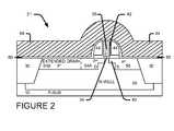
- FIGS. 1A , 1 B, 2 , 3 , 4 , 5 , 6 , 7 A and 7 Bare cross sectional views for illustrating a structure and method for manufacturing a memory device according to an example embodiment of the present invention.
- FIGS. 1A-7Bshow example PFET devices.
- FIG. 7Cis a top down view illustrating a structure and method for manufacturing a memory device according to an example embodiment of the present invention.
- FIG. 8Ais a cross sectional view for illustrating a structure and method for manufacturing a memory device comprised of a NFET in a P-well as part of a two well CMOS approach according to an example embodiment of the present invention.
- FIG. 8Bis a cross sectional view for illustrating a structure and method for manufacturing a memory device comprised of a NFET in a P-well as part of a Triple well CMOS approach according to an example embodiment of the present invention.
- FIG. 9is a schematic diagram of a 1T memory device according to the prior art.
- the example embodimentsprovide a structure and method of forming a memory device such as a one transistor Static Random Access Memory (1T SRAM).
- a memory devicesuch as a one transistor Static Random Access Memory (1T SRAM).
- FIG. 8Aan example completed memory device (e.g., 1T SRAM or DRAM) is shown.
- a point of the some example embodimentsis that the ( FIG. 7A ) capacitor top plate 64 is over a doped bottom plate region 54 B (a portion of the drain element 54 A 54 B).
- SRAMis shown as a NFET. It should be understood that the embodiment is also applicable to NFET or/and PFET type devices. Also, both NFET and PFETs based 1T memory devices (e.g., SRAMs) can be formed concurrently on the same chip.
- isolation region(s) 30surrounding an active region 31 on semiconductor substrate 10 .
- the active region 31is near the surface where the FET will be formed is doped with a first conductivity type dopant, which for a PFET is n-type.
- a n-well 20is formed.
- the isolation regionscan be shallow trench isolation (STI) regions comprised of oxide.
- STIshallow trench isolation
- An example method of forming an example PMOS FETis as follows. Other configurations of the FET (e.g., logic transistors) are possible. The impurity types can be reversed to form a NFET using similar steps. Also, both PMOS and NMOS devices can be form concurrently.
- the substratecan be a monocrystaline Si substrate or any suitable semiconductor substrate or structure.
- the gate dielectric layercan be comprised of any suitable dielectric such as silicon oxide.
- the conductive gate layercan be comprised of polysilicon, silicide and/or metals.
- gate dielectric layer and gate layerWe pattern the gate dielectric layer and gate layer to form gate dielectric 34 and gate electrode 38 .
- the SDE 40can have a boron or any p type impurity.
- the SDE 40can have a dopant concentration between 1E20 and 1E22 atoms/cc.
- the gate spacerscan be comprised of one or more layers.
- the first L spacer 42can be comprised of oxide.
- the second spacer 44can be comprised of nitride.
- source element 50 and drain element 54 A 54 Bwe can implant p-type impurities into the substrate to form source element 50 and drain element 54 A 54 B.
- the gate structure and the isolation regionsare implant masks. If other devices are being formed on other areas of the substrate, a resist layer can be used to demark the appropriate areas for the implant.
- the source element and drain regionare formed from the same conductivity type impurity.
- the source element 50 and drain element 54 A 54 Bcan be formed using the same implant step.
- a feature of the embodimentis that the drain element is comprised of a bottom plate region that is extended or enlarged much more than a typical drain region.
- the drain element 54 A 54 Bmay be comprised of two sections or regions:
- the dopant profile of the extended drain region 54 B(under the capacitor) is preferably substantially the same as the source 50 or drain region 54 A.
- the area of the extended drain region 54 Bis preferably about 2 to 100 times larger than the area of a conventional drain (or of drain region 54 A which does not have a capacitor top plate formed thereover).
- the source element 50 , drain region 54 A and extended drain region 54 Bcan be formed from the same implant step.
- the drain region 54 A and a bottom plate region 54 Bpreferably have substantially the same concentration and depth.
- the source element 50 , drain region 54 A and extended drain region 54 Bcan be have a B, BF2 or any suitable p type dopant, and may have a dopant concentration between about 1E20 and 1E22 atom/cc; and may have depth between 20 nm and 90 nm.
- the implant processcan comprise: implanting B ions at an energy between 5 keV and 30 keV at a dose between 1E14 and 5E15 atoms/square cm.
- the area of plate region 54 Bcan be between 200% and 10000% (2 ⁇ and 100 ⁇ ) as large.
- the dielectric layer 60can be comprised of high-k dielectric (K>3), oxy-nitride or oxide and is preferably comprised of oxide.
- the dielectric layercan have a thickness between 10 and 500 angstroms.
- the conductive layer 64may be comprised of polysilicon, silicon, silicide and is preferably comprised of polysilicon.
- the conductive layer 64can have a thickness between 500 and 2000 angstroms.
- a conductive layer 64 comprised of polysiliconcan be doped with (n or p type impurities depending on the type of FET being formed).
- the conductive layer 64is preferably doped with p at a concentration between 1E20 and 5E22 atoms/cc.
- top plate 64 and capacitor dielectric layer 60can be pattern the conductive layer 64 and the dielectric layer 60 to form a top plate 64 and capacitor dielectric layer 60 over at least a portion of the extended drain region (bottom plate region) 54 B.
- the top plateis over substantially all of the bottom plate region 54 B.
- the top plate 64has sidewalls.
- Some remnants of the dielectric layer 60may remain on the other surfaces. These remnants may be removed.
- top plate spacers 70 Aover the sidewalls of the top plate 64 .
- the spacer layercan be comprised of oxide or nitride and is preferably comprised of oxide.
- the spacer layermay substantially consist of oxide or nitride and preferably of oxide.
- the etchcan remove the remnants of the dielectric layer that could remain of the other surfaces.
- silicide regions 74 A 74 B 74 C and 74 Don the top plate 64 , the drain region 74 B, the source element 50 and the gate electrode 74 C.
- the silicide regionsmay be: the top plate silicide 74 A, drain region silicide 74 B gate silicide 74 C and source region silicide 74 D.
- the silicide regionscan be formed by depositing a suitable metal layer over the surface and annealing.
- interlevel dielectric layer(ILD) 80 over the substrate.
- the ILD layer 80can be comprised of oxide.
- FIG. 7Bshows an electrical schematic overlaid on the embodiment's memory device (such as a SRAM).
- a memory device(e.g., 1T SRAM) can be comprised of:
- FIG. 7Cshows a top down view of the device shown in FIGS. 7A and 7B .
- FIG. 7Cshows word line 88 .
- FIG. 8Aan example completed memory device (e.g., 1T SRAM) is shown.
- a point of the embodimentis that the ( FIG. 7A ) capacitor top plate 64 is over a portion of the drain element 54 A 54 B (e.g., bottom plate region 54 B).
- top plate 64 over the extended drain 54 Bcan have non-limiting features of:
- FIG. 8Ashows an embodiment with NFET memory device (e.g. 1T SRAM) with a double well.
- NFET memory devicee.g. 1T SRAM
- this NFET 1T SRAMFIG. 8A
- PFET 1T SRAMshown in FIG. 7A
- Both PFET and NFET memory devicecan be formed simultaneously on the same chip.
- the capacitoris isolated to the substrate by a PN junction. This prevents any leakages to the substrate. Allows formation of both P and N type 1T SRAM on same chip using double wells. Without the embodiment's PFET bottom plate (extended drain) 154 B, a triple well would be required to prevent shorting of the capacitor to the substrate.
- Example NFET concentrations rangesare listed in the table below.
- FIG. 8Ashows: gate 138 , silicide regions 174 A 174 B 174 C and 174 C, ILD layer 180 , contact 182 , and interconnect 184
- FIG. 8Bshows an embodiment of a NFET 1T SRAM in a triple well process.
- the NFET 1T SRAMcan be formed on the same chip as the FIG. 7A PFET 1T SRAM.
- the thee wellscould the be (1) Nwell 20 (- FIG. 7A ) (2) Pwell 120 ( FIG. 8B ), (3) 3 rd well (N 3 ) 200 ( FIG. 8B ).
- the third well 200 purposeis to further isolate the p-well 120 from the p-substrate 10 .
- this triple well embodimentis not required to form both NFET and PFET 1T SRAMs.
- the second embodiment ( FIGS. 7B and 8A ) with the double wellscan be used to form both NFET and PFET 1T SRAMs.
- Using the third well 200is an optional aspect.
- the example embodiments of the inventioncan be used to make memory devices such as 1T SRAM's and 1T DRAMs.
- the area of the capacitormay need to be increased (compared to a SRAM) to increase the capacitance of the DRAM.
- the example embodimentare not limited to the order of the steps shown.
Landscapes
- Engineering & Computer Science (AREA)
- Manufacturing & Machinery (AREA)
- Semiconductor Memories (AREA)
Abstract
Description
- forming an isolation region surrounding an active region on semiconductor substrate;
- forming a first transistor over an first active region; the first transistor comprised of gate structure, a source element, and a drain element; the source element and drain element are adjacent the gate structure; the source element and drain element are doped with same conductivity type impurity;
- the drain element is comprised of a drain region and a bottom plate region; the drain region is adjacent to the gate structure and the drain region is between the gate structure and the bottom plate region;
- forming a capacitor dielectric layer over the bottom plate region and forming a top plate over the capacitor dielectric layer; the top plate has top plate sidewalls;
- whereby a memory device is comprised of the source element that acts as a bitline, the bottom plate region that acts as a bottom capacitor plate; the capacitor dielectric layer that acts as a capacitor dielectric; the top plate that act as a top capacitor plate.
- an isolation film surrounding an first active area on a substrate;
- a gate dielectric and gate electrode over a portion of the active area;
- a source element and a drain element in the substrate adjacent to the gate electrode; the drain element is comprised of a drain region and a bottom plate region; the bottom plate region is adjacent to the drain region and the isolation film;
- a capacitor dielectric and a capacitor top plate over at least the bottom plate region;
- whereby a 1T memory device is comprised of the source element that acts as a bitline, the gate electrode is connected to a word line; the bottom plate region that acts as a bottom capacitor plate; the capacitor dielectric layer that acts as a capacitor dielectric; the top plate that act as a top capacitor plate.
- (1) a
drain region 54A that is adjacent to thegate electrode 38 and - (2) an
bottom plate region 54B (extendeddrain region 54B) that is between thedrain region 54A and theisolation region 30.
Thebottom plate region 54B (or extended drain region) will act as the bottom plate of a subsequently formed capacitor.
- (1) a
- the
source element 50 acts as a bitline, - the
gate electrode 74C is connected to a word line (FIG. 7C-88 ); - the
bottom plate 54B (e.g. extended drain) acts as a bottom capacitor plate; - the drain region54 a acts as the drain;
- the
capacitor dielectric layer 60 acts as a capacitor dielectric; - the
top plate 64 act as a top capacitor plate.
- the
- the approach is self-aligned where the gate is self aligned to the drain of the transistor
- No additional implant step required to form the bottom plate region
- reduce the overall resistance in the circuit because of the
bottom plate region 54B is doped reduces the resistance - double poly approach (e.g.,38 and64) allows the used of deposition dielectric (i.e, high k materials)
- Smaller dimension of embodiment's memory device (e.g., 1T SRAM) thus greater packing density.
- The embodiments memory device has a minimum spacing between the Gate and the top plate because the drain region is connected to the bottom plate region. (e.g., no undoped region between the
drain region 54A and the bottom plate region56B. - Enables both p and N type 1T memory devices with double well schemes
| Low conc | High conc | |||
| Region Low | Atom/cc | Atom/cc | ||
| p-well 120 | 5E21 | |||
| Drain | ||||
| 154A Bottom plate | 5E22 | |||
| region | ||||
| 154B (n-type) | ||||
| Source 150 (n-type) | 1E18 | 5E22 | ||
| TOP Plate 164 (doped with | 1E20 | 5E22 | ||
| N-typed dopant) | ||||
Claims (29)
Priority Applications (3)
| Application Number | Priority Date | Filing Date | Title |
|---|---|---|---|
| US11/686,475US8716081B2 (en) | 2007-03-15 | 2007-03-15 | Capacitor top plate over source/drain to form a 1T memory device |
| SG201006634-8ASG165374A1 (en) | 2007-03-15 | 2008-02-05 | Capacitor top plate over source/drain to form a 1t memory device |
| SG200801010-0ASG146524A1 (en) | 2007-03-15 | 2008-02-05 | Capacitor top plate over source/drain to form a 1t memory device |
Applications Claiming Priority (1)
| Application Number | Priority Date | Filing Date | Title |
|---|---|---|---|
| US11/686,475US8716081B2 (en) | 2007-03-15 | 2007-03-15 | Capacitor top plate over source/drain to form a 1T memory device |
Publications (2)
| Publication Number | Publication Date |
|---|---|
| US20080224228A1 US20080224228A1 (en) | 2008-09-18 |
| US8716081B2true US8716081B2 (en) | 2014-05-06 |
Family
ID=39761782
Family Applications (1)
| Application Number | Title | Priority Date | Filing Date |
|---|---|---|---|
| US11/686,475Expired - Fee RelatedUS8716081B2 (en) | 2007-03-15 | 2007-03-15 | Capacitor top plate over source/drain to form a 1T memory device |
Country Status (2)
| Country | Link |
|---|---|
| US (1) | US8716081B2 (en) |
| SG (2) | SG165374A1 (en) |
Cited By (2)
| Publication number | Priority date | Publication date | Assignee | Title |
|---|---|---|---|---|
| US9818651B2 (en)* | 2016-03-11 | 2017-11-14 | Globalfoundries Inc. | Methods, apparatus and system for a passthrough-based architecture |
| US11355167B2 (en) | 2018-12-24 | 2022-06-07 | The Trustees Of Columbia University In The City Of New York | Circuits and methods for in-memory computing |
Families Citing this family (7)
| Publication number | Priority date | Publication date | Assignee | Title |
|---|---|---|---|---|
| US7999300B2 (en)* | 2009-01-28 | 2011-08-16 | Globalfoundries Singapore Pte. Ltd. | Memory cell structure and method for fabrication thereof |
| KR101842439B1 (en)* | 2011-12-22 | 2018-03-29 | 삼성전자주식회사 | Semiconductor device |
| US9722081B1 (en)* | 2016-01-29 | 2017-08-01 | Taiwan Semiconductor Manufacturing Co., Ltd. | FinFET device and method of forming the same |
| TWI595653B (en)* | 2016-09-13 | 2017-08-11 | 立積電子股份有限公司 | Transistor for increasing the amplitude range of the signal |
| WO2019125497A1 (en)* | 2017-12-22 | 2019-06-27 | Intel Corporation | Interconnect structures for integrated circuits |
| TWI696247B (en)* | 2019-01-28 | 2020-06-11 | 力晶積成電子製造股份有限公司 | Memory structure |
| US11532669B2 (en)* | 2019-08-23 | 2022-12-20 | Taiwan Semiconductor Manufacturing Co., Ltd. | Memory device and manufacturing method thereof |
Citations (18)
| Publication number | Priority date | Publication date | Assignee | Title |
|---|---|---|---|---|
| US4894693A (en)* | 1985-05-01 | 1990-01-16 | Tigelaar Howard L | Single-polysilicon dram device and process |
| US5382807A (en) | 1991-05-09 | 1995-01-17 | Mitsubishi Denki Kabushiki Kaisha | Field effect thin film transistor and static-type semiconductor memory device provided with memory cell having complementary field effect transistor and method of manufacturing the same |
| US5492853A (en) | 1994-03-11 | 1996-02-20 | Micron Semiconductor, Inc. | Method of forming a contact using a trench and an insulation layer during the formation of a semiconductor device |
| US5814867A (en) | 1995-04-14 | 1998-09-29 | Sharp Kabushiki Kaisha | Semiconductor device and fabrication method thereof |
| US5894163A (en)* | 1996-04-02 | 1999-04-13 | Motorola, Inc. | Device and method for multiplying capacitance |
| US6177697B1 (en)* | 1998-04-29 | 2001-01-23 | Philips Semiconductors, Inc. | Arrangement for DRAM cell using shallow trench isolation |
| US6307251B1 (en) | 1998-11-27 | 2001-10-23 | Sanyo Electric Co., Ltd. | Semiconductor device having capacitance element and method of producing the same |
| US20010054727A1 (en)* | 1998-12-03 | 2001-12-27 | Franz Hofmann | Integrated circuit configuration and method for manufacturing it |
| US20020094611A1 (en)* | 2001-01-16 | 2002-07-18 | Taiwan Semiconductor Manufacturing Co., Ltd. | Low programming voltage anti-fuse structure |
| US6483139B1 (en)* | 2001-07-05 | 2002-11-19 | Mitsubishi Denki Kabushiki Kaisha | Semiconductor memory device formed on semiconductor substrate |
| US20030001181A1 (en)* | 1998-08-14 | 2003-01-02 | Monolithic System Technology, Inc. | Method of fabricating a DRAM cell having a thin dielectric access transistor and a thick dielectric storage capacitor |
| US20040155298A1 (en)* | 2003-02-12 | 2004-08-12 | Arup Bhattacharyya | Memory devices and electronic systems comprising integrated bipolar and FET devices |
| US6787836B2 (en) | 2002-08-21 | 2004-09-07 | International Business Machines Corporation | Integrated metal-insulator-metal capacitor and metal gate transistor |
| US6790724B1 (en) | 2001-02-20 | 2004-09-14 | Taiwan Semiconductor Manufacturing Company | Low leakage one transistor static random access memory |
| US20050098905A1 (en) | 2003-11-11 | 2005-05-12 | Tzung-Han Lee | SRAM cell structure and manufacturing method thereof |
| US20070080387A1 (en)* | 2005-10-07 | 2007-04-12 | Taiwan Semiconductor Manufacturing Company, Ltd. | Method and structure for a 1T-RAM bit cell and macro |
| US7447064B1 (en)* | 2006-03-27 | 2008-11-04 | National Semiconductor Corporation | System and method for providing a CMOS compatible single poly EEPROM with an NMOS program transistor |
| US7465639B1 (en)* | 2005-05-20 | 2008-12-16 | Advanced Micro Devices, Inc. | Method for fabricating an SOI device |
- 2007
- 2007-03-15USUS11/686,475patent/US8716081B2/ennot_activeExpired - Fee Related
- 2008
- 2008-02-05SGSG201006634-8Apatent/SG165374A1/enunknown
- 2008-02-05SGSG200801010-0Apatent/SG146524A1/enunknown
Patent Citations (20)
| Publication number | Priority date | Publication date | Assignee | Title |
|---|---|---|---|---|
| US4894693A (en)* | 1985-05-01 | 1990-01-16 | Tigelaar Howard L | Single-polysilicon dram device and process |
| US5382807A (en) | 1991-05-09 | 1995-01-17 | Mitsubishi Denki Kabushiki Kaisha | Field effect thin film transistor and static-type semiconductor memory device provided with memory cell having complementary field effect transistor and method of manufacturing the same |
| US5492853A (en) | 1994-03-11 | 1996-02-20 | Micron Semiconductor, Inc. | Method of forming a contact using a trench and an insulation layer during the formation of a semiconductor device |
| US5814867A (en) | 1995-04-14 | 1998-09-29 | Sharp Kabushiki Kaisha | Semiconductor device and fabrication method thereof |
| US5894163A (en)* | 1996-04-02 | 1999-04-13 | Motorola, Inc. | Device and method for multiplying capacitance |
| US6177697B1 (en)* | 1998-04-29 | 2001-01-23 | Philips Semiconductors, Inc. | Arrangement for DRAM cell using shallow trench isolation |
| US20030001181A1 (en)* | 1998-08-14 | 2003-01-02 | Monolithic System Technology, Inc. | Method of fabricating a DRAM cell having a thin dielectric access transistor and a thick dielectric storage capacitor |
| US6307251B1 (en) | 1998-11-27 | 2001-10-23 | Sanyo Electric Co., Ltd. | Semiconductor device having capacitance element and method of producing the same |
| US6670236B2 (en) | 1998-11-27 | 2003-12-30 | Sanyo Electric Co., Ltd. | Semiconductor device having capacitance element and method of producing the same |
| US20010054727A1 (en)* | 1998-12-03 | 2001-12-27 | Franz Hofmann | Integrated circuit configuration and method for manufacturing it |
| US20020094611A1 (en)* | 2001-01-16 | 2002-07-18 | Taiwan Semiconductor Manufacturing Co., Ltd. | Low programming voltage anti-fuse structure |
| US6790724B1 (en) | 2001-02-20 | 2004-09-14 | Taiwan Semiconductor Manufacturing Company | Low leakage one transistor static random access memory |
| US20050009271A1 (en) | 2001-02-20 | 2005-01-13 | Pin-Shyne Chin | Low leakage one transistor static random access memory |
| US6483139B1 (en)* | 2001-07-05 | 2002-11-19 | Mitsubishi Denki Kabushiki Kaisha | Semiconductor memory device formed on semiconductor substrate |
| US6787836B2 (en) | 2002-08-21 | 2004-09-07 | International Business Machines Corporation | Integrated metal-insulator-metal capacitor and metal gate transistor |
| US20040155298A1 (en)* | 2003-02-12 | 2004-08-12 | Arup Bhattacharyya | Memory devices and electronic systems comprising integrated bipolar and FET devices |
| US20050098905A1 (en) | 2003-11-11 | 2005-05-12 | Tzung-Han Lee | SRAM cell structure and manufacturing method thereof |
| US7465639B1 (en)* | 2005-05-20 | 2008-12-16 | Advanced Micro Devices, Inc. | Method for fabricating an SOI device |
| US20070080387A1 (en)* | 2005-10-07 | 2007-04-12 | Taiwan Semiconductor Manufacturing Company, Ltd. | Method and structure for a 1T-RAM bit cell and macro |
| US7447064B1 (en)* | 2006-03-27 | 2008-11-04 | National Semiconductor Corporation | System and method for providing a CMOS compatible single poly EEPROM with an NMOS program transistor |
Cited By (4)
| Publication number | Priority date | Publication date | Assignee | Title |
|---|---|---|---|---|
| US9818651B2 (en)* | 2016-03-11 | 2017-11-14 | Globalfoundries Inc. | Methods, apparatus and system for a passthrough-based architecture |
| US10559503B2 (en)* | 2016-03-11 | 2020-02-11 | Globalfoundries Inc. | Methods, apparatus and system for a passthrough-based architecture |
| US11355167B2 (en) | 2018-12-24 | 2022-06-07 | The Trustees Of Columbia University In The City Of New York | Circuits and methods for in-memory computing |
| US11783875B2 (en) | 2018-12-24 | 2023-10-10 | The Trustees Of Columbia University In The City Of New York | Circuits and methods for in-memory computing |
Also Published As
| Publication number | Publication date |
|---|---|
| SG165374A1 (en) | 2010-10-28 |
| US20080224228A1 (en) | 2008-09-18 |
| SG146524A1 (en) | 2008-10-30 |
Similar Documents
| Publication | Publication Date | Title |
|---|---|---|
| US5547893A (en) | method for fabricating an embedded vertical bipolar transistor and a memory cell | |
| US8716081B2 (en) | Capacitor top plate over source/drain to form a 1T memory device | |
| US7193262B2 (en) | Low-cost deep trench decoupling capacitor device and process of manufacture | |
| KR101497802B1 (en) | Double Channel Doping in Transistor Formation | |
| JP4773169B2 (en) | Manufacturing method of semiconductor device | |
| US6274467B1 (en) | Dual work function gate conductors with self-aligned insulating cap | |
| US20130114333A1 (en) | Semiconductor memory device and fabrication process thereof | |
| US8946821B2 (en) | SRAM integrated circuits and methods for their fabrication | |
| US6399987B2 (en) | MOS transistor having self-aligned well bias area | |
| US20080179676A1 (en) | Semiconductor memory device | |
| US8797787B2 (en) | Semiconductor manufacturing method | |
| US7868461B2 (en) | Embedded interconnects, and methods for forming same | |
| US8324666B2 (en) | DRAM cell transistor device and method | |
| US5981324A (en) | Methods of forming integrated circuits having memory cell arrays and peripheral circuits therein | |
| US20070018253A1 (en) | Memory cell and manufacturing methods | |
| US6974987B2 (en) | Semiconductor device | |
| US7718482B2 (en) | CD gate bias reduction and differential N+ poly doping for CMOS circuits | |
| US6690071B2 (en) | Semiconductor device using junction leak current | |
| US6864506B2 (en) | SRAM cell and method for fabricating the same | |
| US20090001481A1 (en) | Digital circuits having additional capacitors for additional stability | |
| US8546890B2 (en) | Inverter structure and method for fabricating the same | |
| JP2005236135A (en) | Manufacturing method of semiconductor device | |
| US7588991B2 (en) | Method for fabricating embedded static random access memory | |
| TWI433275B (en) | Inverter structure and method for fabricating the same | |
| KR100855862B1 (en) | ESR (SRAAM) cell and manufacturing method thereof |
Legal Events
| Date | Code | Title | Description |
|---|---|---|---|
| AS | Assignment | Owner name:CHARTERED SEMICONDUCTOR MANUFACTURING LTD., SINGAP Free format text:ASSIGNMENT OF ASSIGNORS INTEREST;ASSIGNORS:TEO, LEE WEE;LEE, YONG MENG;LUN, ZHAO;AND OTHERS;REEL/FRAME:019071/0631;SIGNING DATES FROM 20061030 TO 20070228 Owner name:CHARTERED SEMICONDUCTOR MANUFACTURING LTD., SINGAP Free format text:ASSIGNMENT OF ASSIGNORS INTEREST;ASSIGNORS:TEO, LEE WEE;LEE, YONG MENG;LUN, ZHAO;AND OTHERS;SIGNING DATES FROM 20061030 TO 20070228;REEL/FRAME:019071/0631 | |
| FEPP | Fee payment procedure | Free format text:PAYOR NUMBER ASSIGNED (ORIGINAL EVENT CODE: ASPN); ENTITY STATUS OF PATENT OWNER: LARGE ENTITY | |
| AS | Assignment | Owner name:CHARTERED SEMICONDUCTOR MANUFACTURING PTE. LTD. , Free format text:CHANGE OF NAME;ASSIGNOR:CHARTERED SEMICONDUCTOR MANUFACTURING LTD. ;REEL/FRAME:032421/0671 Effective date:20100115 Owner name:GLOBALFOUNDRIES SINGAPORE PTE. LTD. , SINGAPORE Free format text:CHANGE OF NAME;ASSIGNOR:CHARTERED SEMICONDUCTOR MANUFACTURING PTE. LTD. ;REEL/FRAME:032421/0669 Effective date:20100115 | |
| STCF | Information on status: patent grant | Free format text:PATENTED CASE | |
| MAFP | Maintenance fee payment | Free format text:PAYMENT OF MAINTENANCE FEE, 4TH YEAR, LARGE ENTITY (ORIGINAL EVENT CODE: M1551) Year of fee payment:4 | |
| AS | Assignment | Owner name:WILMINGTON TRUST, NATIONAL ASSOCIATION, DELAWARE Free format text:SECURITY AGREEMENT;ASSIGNOR:GLOBALFOUNDRIES SINGAPORE PTE. LTD.;REEL/FRAME:047660/0203 Effective date:20181127 | |
| AS | Assignment | Owner name:GLOBALFOUNDRIES SINGAPORE PTE. LTD., SINGAPORE Free format text:RELEASE BY SECURED PARTY;ASSIGNOR:WILMINGTON TRUST, NATIONAL ASSOCIATION;REEL/FRAME:054481/0673 Effective date:20201117 | |
| LAPS | Lapse for failure to pay maintenance fees | Free format text:PATENT EXPIRED FOR FAILURE TO PAY MAINTENANCE FEES (ORIGINAL EVENT CODE: EXP.); ENTITY STATUS OF PATENT OWNER: LARGE ENTITY | |
| FEPP | Fee payment procedure | Free format text:MAINTENANCE FEE REMINDER MAILED (ORIGINAL EVENT CODE: REM.); ENTITY STATUS OF PATENT OWNER: LARGE ENTITY | |
| STCH | Information on status: patent discontinuation | Free format text:PATENT EXPIRED DUE TO NONPAYMENT OF MAINTENANCE FEES UNDER 37 CFR 1.362 | |
| FP | Lapsed due to failure to pay maintenance fee | Effective date:20220506 |