US8715788B1 - Method to improve mechanical strength of low-K dielectric film using modulated UV exposure - Google Patents
Method to improve mechanical strength of low-K dielectric film using modulated UV exposureDownload PDFInfo
- Publication number
- US8715788B1 US8715788B1US13/275,209US201113275209AUS8715788B1US 8715788 B1US8715788 B1US 8715788B1US 201113275209 AUS201113275209 AUS 201113275209AUS 8715788 B1US8715788 B1US 8715788B1
- Authority
- US
- United States
- Prior art keywords
- dielectric layer
- film
- dielectric
- modulated
- radiation
- Prior art date
- Legal status (The legal status is an assumption and is not a legal conclusion. Google has not performed a legal analysis and makes no representation as to the accuracy of the status listed.)
- Expired - Lifetime, expires
Links
Images


Classifications
- H—ELECTRICITY
- H01—ELECTRIC ELEMENTS
- H01L—SEMICONDUCTOR DEVICES NOT COVERED BY CLASS H10
- H01L21/00—Processes or apparatus adapted for the manufacture or treatment of semiconductor or solid state devices or of parts thereof
- H01L21/02—Manufacture or treatment of semiconductor devices or of parts thereof
- H01L21/02104—Forming layers
- H01L21/02107—Forming insulating materials on a substrate
- H01L21/02296—Forming insulating materials on a substrate characterised by the treatment performed before or after the formation of the layer
- H01L21/02318—Forming insulating materials on a substrate characterised by the treatment performed before or after the formation of the layer post-treatment
- H01L21/02345—Forming insulating materials on a substrate characterised by the treatment performed before or after the formation of the layer post-treatment treatment by exposure to radiation, e.g. visible light
- H01L21/02348—Forming insulating materials on a substrate characterised by the treatment performed before or after the formation of the layer post-treatment treatment by exposure to radiation, e.g. visible light treatment by exposure to UV light
- H—ELECTRICITY
- H01—ELECTRIC ELEMENTS
- H01L—SEMICONDUCTOR DEVICES NOT COVERED BY CLASS H10
- H01L21/00—Processes or apparatus adapted for the manufacture or treatment of semiconductor or solid state devices or of parts thereof
- H01L21/02—Manufacture or treatment of semiconductor devices or of parts thereof
- H01L21/04—Manufacture or treatment of semiconductor devices or of parts thereof the devices having potential barriers, e.g. a PN junction, depletion layer or carrier concentration layer
- H01L21/18—Manufacture or treatment of semiconductor devices or of parts thereof the devices having potential barriers, e.g. a PN junction, depletion layer or carrier concentration layer the devices having semiconductor bodies comprising elements of Group IV of the Periodic Table or AIIIBV compounds with or without impurities, e.g. doping materials
- H01L21/30—Treatment of semiconductor bodies using processes or apparatus not provided for in groups H01L21/20 - H01L21/26
- H01L21/31—Treatment of semiconductor bodies using processes or apparatus not provided for in groups H01L21/20 - H01L21/26 to form insulating layers thereon, e.g. for masking or by using photolithographic techniques; After treatment of these layers; Selection of materials for these layers
- H01L21/3105—After-treatment
- H—ELECTRICITY
- H01—ELECTRIC ELEMENTS
- H01L—SEMICONDUCTOR DEVICES NOT COVERED BY CLASS H10
- H01L21/00—Processes or apparatus adapted for the manufacture or treatment of semiconductor or solid state devices or of parts thereof
- H01L21/02—Manufacture or treatment of semiconductor devices or of parts thereof
- H01L21/02104—Forming layers
- H01L21/02107—Forming insulating materials on a substrate
- H01L21/02109—Forming insulating materials on a substrate characterised by the type of layer, e.g. type of material, porous/non-porous, pre-cursors, mixtures or laminates
- H01L21/02112—Forming insulating materials on a substrate characterised by the type of layer, e.g. type of material, porous/non-porous, pre-cursors, mixtures or laminates characterised by the material of the layer
- H01L21/02123—Forming insulating materials on a substrate characterised by the type of layer, e.g. type of material, porous/non-porous, pre-cursors, mixtures or laminates characterised by the material of the layer the material containing silicon
- H01L21/02126—Forming insulating materials on a substrate characterised by the type of layer, e.g. type of material, porous/non-porous, pre-cursors, mixtures or laminates characterised by the material of the layer the material containing silicon the material containing Si, O, and at least one of H, N, C, F, or other non-metal elements, e.g. SiOC, SiOC:H or SiONC
- H—ELECTRICITY
- H01—ELECTRIC ELEMENTS
- H01L—SEMICONDUCTOR DEVICES NOT COVERED BY CLASS H10
- H01L21/00—Processes or apparatus adapted for the manufacture or treatment of semiconductor or solid state devices or of parts thereof
- H01L21/02—Manufacture or treatment of semiconductor devices or of parts thereof
- H01L21/02104—Forming layers
- H01L21/02107—Forming insulating materials on a substrate
- H01L21/02109—Forming insulating materials on a substrate characterised by the type of layer, e.g. type of material, porous/non-porous, pre-cursors, mixtures or laminates
- H01L21/02203—Forming insulating materials on a substrate characterised by the type of layer, e.g. type of material, porous/non-porous, pre-cursors, mixtures or laminates the layer being porous
- H—ELECTRICITY
- H01—ELECTRIC ELEMENTS
- H01L—SEMICONDUCTOR DEVICES NOT COVERED BY CLASS H10
- H01L21/00—Processes or apparatus adapted for the manufacture or treatment of semiconductor or solid state devices or of parts thereof
- H01L21/02—Manufacture or treatment of semiconductor devices or of parts thereof
- H01L21/02104—Forming layers
- H01L21/02107—Forming insulating materials on a substrate
- H01L21/02109—Forming insulating materials on a substrate characterised by the type of layer, e.g. type of material, porous/non-porous, pre-cursors, mixtures or laminates
- H01L21/02205—Forming insulating materials on a substrate characterised by the type of layer, e.g. type of material, porous/non-porous, pre-cursors, mixtures or laminates the layer being characterised by the precursor material for deposition
- H01L21/02208—Forming insulating materials on a substrate characterised by the type of layer, e.g. type of material, porous/non-porous, pre-cursors, mixtures or laminates the layer being characterised by the precursor material for deposition the precursor containing a compound comprising Si
- H01L21/02214—Forming insulating materials on a substrate characterised by the type of layer, e.g. type of material, porous/non-porous, pre-cursors, mixtures or laminates the layer being characterised by the precursor material for deposition the precursor containing a compound comprising Si the compound comprising silicon and oxygen
- H01L21/02216—Forming insulating materials on a substrate characterised by the type of layer, e.g. type of material, porous/non-porous, pre-cursors, mixtures or laminates the layer being characterised by the precursor material for deposition the precursor containing a compound comprising Si the compound comprising silicon and oxygen the compound being a molecule comprising at least one silicon-oxygen bond and the compound having hydrogen or an organic group attached to the silicon or oxygen, e.g. a siloxane
- H—ELECTRICITY
- H01—ELECTRIC ELEMENTS
- H01L—SEMICONDUCTOR DEVICES NOT COVERED BY CLASS H10
- H01L21/00—Processes or apparatus adapted for the manufacture or treatment of semiconductor or solid state devices or of parts thereof
- H01L21/02—Manufacture or treatment of semiconductor devices or of parts thereof
- H01L21/02104—Forming layers
- H01L21/02107—Forming insulating materials on a substrate
- H01L21/02225—Forming insulating materials on a substrate characterised by the process for the formation of the insulating layer
- H01L21/0226—Forming insulating materials on a substrate characterised by the process for the formation of the insulating layer formation by a deposition process
- H01L21/02263—Forming insulating materials on a substrate characterised by the process for the formation of the insulating layer formation by a deposition process deposition from the gas or vapour phase
- H01L21/02271—Forming insulating materials on a substrate characterised by the process for the formation of the insulating layer formation by a deposition process deposition from the gas or vapour phase deposition by decomposition or reaction of gaseous or vapour phase compounds, i.e. chemical vapour deposition
- H01L21/02274—Forming insulating materials on a substrate characterised by the process for the formation of the insulating layer formation by a deposition process deposition from the gas or vapour phase deposition by decomposition or reaction of gaseous or vapour phase compounds, i.e. chemical vapour deposition in the presence of a plasma [PECVD]
Definitions
- This inventionrelates to methods and apparatus for preparing dielectric films for integrated circuits, particularly carbon-doped oxide (CDO) dielectric films. More specifically, the invention employs modulated ultraviolet radiation to increase the hardness and modulus of the film. In preferred embodiments, the film shrinkage and dielectric constant are minimally affected.
- CDOcarbon-doped oxide
- Low-k materialsas the inter-metal and/or inter-layer dielectric in integrated circuits reduces the delay in signal propagation due to capacitive effects.
- Low k dielectricsare conventionally defined as those materials that have a dielectric constant lower than that of silicon dioxide, that is k ⁇ 4.
- Methods of obtaining these ultra low-k materialsinclude doping silicon dioxide with carbon to create a carbon-doped oxide (CDO), or incorporating air voids within a low-k dielectric to create a porous dielectric material, or a combination of both (i.e., creating a CDO porous dielectric).
- CDOcarbon-doped oxide
- the present inventionaddresses this need by providing methods for improving the mechanical properties of a dielectric film on a partially fabricated integrated circuit while limiting shrinkage and limiting any increase in dielectric constant.
- Methodsinclude (a) providing the partially fabricated integrated circuit having a low-k dielectric film formed thereon, (b) exposing the dielectric film to UV radiation of modulated intensity to thereby improve the mechanical properties of the dielectric film while limiting shrinkage and limiting any increases in dielectric constant and (c) forming one or more additional layers on the partially fabricated integrated circuit.
- the low-k dielectric filmmay be a porous or non-porous (sometimes referred as “dense”) dielectric film.
- CDOcarbon-doped silicon oxides
- silicon oxidemay be doped with fluorine and/or other elements and even metals.
- the CDO filmsare comprised of carbon (typically in the form of methyl or other hydrocarbon groups) in addition to silicon and oxygen.
- precursorsare available to produce CDO films. These include various carbon containing compounds and silicon containing compounds. In many cases, a single precursor compound will include silicon, carbon, and sometimes oxygen.
- the precursor filmis formed by co-depositing the porogen with the structure former.
- the porogenis frequently, but not necessarily, an organic material and the structure former a silicon-containing material.
- the structure formercan be produced from silanes, alkylsilanes (e.g., trimethylsilane, di-tert-butylsilane and tetramethylsilane), alkoxysilanes (e.g., methyltriethoxysilane (MTEOS), methyltrimethoxysilane (MTMOS) diethoxymethylsilane (DEMS), methyldimethoxysilane (MDMOS), trimethylmethoxysilane (TMMOS) and dimethyldimethoxysilane (DMDMOS)), linear siloxanes, cyclic siloxanes (e.g.
- octamethylcyclotetrasiloxaneand tetramethylcyclotetrasiloxane (TMCTS)
- silylalkenese.g., vinyltrimethylsilane (VTMS)
- silylalkynese.g., trimethylsilylacetylene (TMSA), bis-trimethylsilylacetylene (BTMSA), or a combination thereof.
- TMSAtrimethylsilylacetylene
- BTMSAbis-trimethylsilylacetylene
- porogen compoundsis the polyfunctional cyclic non-aromatic compounds.
- terpeninessuch as alpha terpenine (ATRP)
- norborenessuch as 5-ethylidene-2-norbornene (ENB), limonene (C 2 H 5 OH) and other related compounds.
- the dielectricmay be of the “high density” variety (substantially pore free) or the “low density” variety (porous).
- the pores in porous filmscan be of many different sizes, ranging from nanometer scale to micron scale depending on the application. Regardless of its structure and composition, the material preferably has a relatively low dielectric constant (e.g., less than about 4, and more typically less than about 3) and relatively high mechanical strength. In many applications, the thickness of the dielectric film is between about 50 Angstroms and 5 micrometers and more preferably between about 500 Angstroms and 5,000 Angstroms.
- Improvements of the mechanical properties of the dielectric film as a result of using methods of the inventioninclude improvements in the hardness and stiffness of the film.
- the hardness of a nonporous filmis preferably increased by about 0.3 GPa or greater and more preferably it is increased by about 0.7 GPa or greater (which corresponds to a increase in modulus of about 4.6 GPa or greater).
- the hardness of a porous filmis preferably increased by about 0.9 Gpa or greater (which corresponds to a increase in modulus of about 5.0 GPa or greater).
- the dielectric non-porous filmshrinks by no more than about 10% and the dielectric constant increases by no more than about 1% whereas a porous film will preferably shrink by no more than about 25% and more preferably by no more than about 15% and the dielectric constant increases by no more than about 8% and more preferably by no more than about 4%.
- the present inventioninvolves exposing the dielectric film to a UV source that produces modulated or oscillating UV radiation at the substrate surface.
- a UV sourcethat produces modulated or oscillating UV radiation at the substrate surface.
- the choices of UV wavelength(s), total exposure time and intensity, modulation period and amplitude, etc.depend on a number of factors, including the thickness of the dielectric film and the composition of the dielectric film.
- the oscillating UV radiationhas a period of between about 1 ⁇ seconds and 5 minutes, and more preferably between about 1 millisecond and 30 seconds.
- the duty cycle of the UV sourcepreferably ranges between about 1% and about 90%.
- the total exposure time to oscillating UV radiationis preferably between about 1 second and about 60 minutes.
- the amplitude (i.e., intensity variation) of the UV radiationwill preferably vary between about 0 and 3 Watts/cm 2 .
- Typical wavelengths used for CDO filmsrange between about 150 nm and 800 nm.
- the apparatus employed to implement the inventioncan have one or more UV sources.
- the apparatuswill have a single UV source.
- the modulationmay be introduced by any of many different mechanisms for controlling the UV radiation delivered to the work piece. Examples include controlling UV source power, controlling mechanical barriers (e.g., an aperture or rotating chopper) between the UV source and the substrate, and controlling an optical element (e.g., a filter, lens, or mirror) between the source and the substrate.
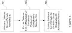
- FIG. 1is a flowchart summarizing stages of example implementations of the invention.
- FIG. 2is a chart representing an example of modulated UV exposure as a function of time in accordance with the invention.
- FIG. 3is a chart representing film shrinkage as a function of UV exposure time using continuous and modulated UV exposure modes.
- FIG. 4is a chart representing film dielectric constant as a function of UV exposure time using continuous and modulated UV exposure modes.
- FIG. 5is a schematic representation of an UV apparatus suitable for film treatment in accordance with some embodiments of this invention.
- semiconductor substratesinclude any semiconductor substrate at any of the various states of manufacture/fabrication in the production of integrated circuits.
- the concept of a semiconductor substrateincludes whole wafers and dies, partially fabricated integrated circuits and completely fabricated integrated circuits, whether or not packaged, and the like.
- CDOcarbon-doped silicon oxide
- thesecan have various amounts of carbon (typically in the form of hydrocarbon groups such as methyl and/or methylene groups) depending upon desired film qualities and applications.
- methods of the inventionare not limited to CDO films.
- the methodsmay also be used to effectively strengthen silicon dioxide films containing other dopants such as fluorine or various metals.
- the inventionmay also extend to undoped silicon oxide films and even non-silicon dioxide based dielectric materials.
- the present inventioncan be used on both porous and non-porous (sometimes referred to as “dense”) dielectric films.
- Any suitable method for forming a non-porous dielectric filmmay be used.
- One methodinvolves PECVD methods using a silane, silane derivative, siloxane, siloxane derivative or a combination of two or more of these compounds.
- Methods of fabricating porous filmstypically involve forming a composite film (referred to herein as a “precursor film”) containing two components: a porogen (typically an organic material of low or high molecular weight (e.g., a polymer)) and a structure former or dielectric material (e.g., a silicon containing material).
- a porogentypically an organic material of low or high molecular weight (e.g., a polymer)
- a structure former or dielectric materiale.g., a silicon containing material
- porogen componentis removed, leaving a structurally intact porous low-k dielectric matrix.
- porogens and porogen-removal techniquesare described in U.S. patent application Ser. No. 10/800,377, previously incorporated by reference.
- a porogenis any removable material that defines void regions in a dielectric matrix.
- the porogenmay be removed by thermal methods, treatment with plasma, supercritical extraction, UV-mediated techniques, electron beam treatment and the like.
- the dielectric film(or precursor film in the case of a porous dielectric) may be formed by any of numerous techniques. Examples include spin-coating processes, print-on, dip coating, thermal process, supercritical deposition process, and chemical vapor deposition—particularly plasma enhanced chemical vapor deposition (PECVD).
- PECVDplasma enhanced chemical vapor deposition
- a methylsilsesquioxane filmis formed using spin-on-glass techniques.
- the filmis deposited using standard CVD or PECVD methods in which organo-silane precursors such as methylsilanes are used with oxidizing agents such as oxygen, nitrous oxide or carbon dioxide, or an inert gas such as nitrogen, argon, helium, or a mixture of oxidizing gas and inert gas.
- a range of examples of precursors for the dielectric filmincludes silane, alkylsilanes (e.g., trimethylsilane, di-tert-butylsilane, and tetramethylsilane), alkoxysilanes (e.g., tetraethoxysilane (TEOS), methyltriethoxysilane (MTEOS), methyltrimethoxysilane (MTMOS) diethoxymethylsilane (DEMS), methyldimethoxysilane (MDMOS), trimethylmethoxysilane (TMMOS) and dimethyldimethoxysilane (DMDMOS)), linear siloxanes and cyclic siloxanes (e.g.
- alkylsilanese.g., trimethylsilane, di-tert-butylsilane, and tetramethylsilane
- alkoxysilanese.g., tetraethoxysilane (TEOS
- octamethylcyclotetrasiloxaneOCTS
- TMCtetramethylcyclotetrasiloxane
- silylalkenese.g., vinyltrimethylsilane (VTMS)
- silylalkynese.g., trimethylsilylacetylene (TMSA), bis-trimethylsilylacetylene (BTMSA).
- Any suitable methodmay be used to deposit the dielectric film, including a PECVD method.
- the thickness of the dielectric layerdepends upon the ultimate application. As an example, the thickness may range between about 50 to 1500 angstroms for a hard mask application. For an interlayer dielectric or packaging application, the thickness may range up to about 2 to 3 microns. In some cases, extra thickness is required to provide some amount of sacrificial dielectric to accommodate a subsequent planarization or polishing step. In some cases, the thickness of the precursor layer may be driven in part by the ability of the UV radiation to penetrate the film and remove the porogen. Therefore, relatively thinner precursor layers may be required for some processes.
- Methods of the inventioninvolve improving 1) the “mechanical performance” of the porous low-k dielectric film, 2) with minimal k value increase, and 3) with minimal film shrinkage.
- Mechanical performancemay be manifest in terms of hardness, modulus, intrinsic stress, etc. Hardness and modulus are well defined within the art and will not be discussed in detail herein. Measures of film hardness and modulus presented herein may be made with any suitable apparatus including nano-indenter device.
- a “cracking threshold” measurementis a measure of thickness of a dielectric film on a blank substrate (e.g., a flat 200 mm wafer) that can be deposited without forming a crack.
- the dielectricis deposited to various thicknesses using a single set of process conditions.
- the resulting wafer (with dielectric film)is set aside without disturbance for a period of time (e.g., one day) and then examined for cracks.
- the greatest thickness at which no crack is observedis the cracking threshold.
- the cracking thresholdis measured in micrometers.
- UV radiation used with the inventionencompasses near-UV, far-UV, as well as UV wavelengths. Some films may be more effectively treated using UV light with particular ranges of wavelengths and/or intensities.
- the intensity of the UV radiationis modulated and typically oscillating.
- the modulated UV radiationcan be achieved in any number of ways including providing a UV light source adapted to providing intermittent UV light intensities, providing more than one UV light source that can be turned on and off intermittently, shielding the substrate from UV exposure intermittently by using a shutter or light deflector (lens or mirror) for example, or moving the substrate intermittently in and out of the UV radiation exposure area.
- Dielectric film exposure to UV radiation in generalhas been studied previously for various applications, including for porogen removal as well as mechanical strengthening applications. These applications of UV exposure are discussed, for example, in the previously referenced U.S. patent application Ser. No. 10/404,693, and U.S. patent application Ser. No. 10/800,377, both previously incorporated by reference.
- the present inventionfocuses on using modulated or oscillating UV exposure.
- FIG. 1provides a flow chart depicting one general high-level process flow in accordance with some embodiments of the present invention.
- a dielectric filmis provided on a substrate as indicated by a process block 101 .
- the thickness of the dielectric filmwill depend upon the ultimate application.
- porous filmshave lower dielectric constants than non-porous CDO films.
- porous filmstypically have k values ranging between about 1.8 and 2.8 whereas non-porous CDO films typically have k values ranging between about 2.4 and 4.0.
- various techniques for forming a CDO filmmay be employed. It is noted again that the invention is not limited to any particular type of dielectric film or deposition method.
- the dielectric film, provided at block 101is exposed to modulated UV radiation, as indicated at block 103 .
- the modulated UV radiationcan be achieved using any of a number of techniques.
- one UV radiation sourcethat is capable of providing modulated UV intensities, is used.
- An example of a suitable apparatus for the inventionis described in further detail.
- additional layer(s) as required by the IC manufacturing processis/are formed over the dielectric film. See block 105 .
- the dielectric filmis etched with vias and/or trenches before the additional layer(s) is/are deposited. After operation 105 , the process flow of FIG. 1 is complete.
- FIG. 2is a graphical representation of UV exposure as a function of time in accordance with an example of the present invention.
- UV Intensity (y-axis) and Time (x-axis)are in arbitrary units.
- UV radiation reaching the substrateis modulated between Level 1 intensity and Level 2 intensity.
- Level 1 intensityis higher than Level 2 intensity.
- Substrate exposure to Level 1 intensityoccurs periodically at intervals with particular time durations and exposure to Level 2 intensity occurs periodically at intervals with other time durations. As shown, the period of oscillation is given by time 201 .
- Level 1 phaseis about twice the duration of Level 2 phase.
- Level 2 intensitywas zero (as would occur if the UV light source was turned OFF or blocked during Level 2 phases)
- the duty cycle of the UV light sourcewould be 67% (i.e., ON two thirds of the time and OFF one third of the time).
- the graph of FIG. 2shows four cycles of Level 1 exposures, but of course any number of cycles of exposures can be used as necessary to effect improvement in the dielectric layer's mechanical properties.
- the modulationmay impact the process. These include the maximum and minimum intensity levels, the period of the modulation cycle, the duty cycle, the total exposure time.
- the light intensity amplitudemay be between about 1 ⁇ W/cm 2 and 3 W/cm 2 .
- the minimum light intensity levelis 0 (e.g., light source is turned OFF), although this is not necessary.
- the period of the modulationmay be between about 1 ⁇ s seconds and 10 minutes, for example. For at least some CDO films, it has been found that a cycle period of between about 1 seconds and 30 seconds works well.
- the duty cycle(e.g., percentage of time the light source is ON) is preferably between about 1% and 90% and more preferably between 10% and 80%.
- the total time during which the dielectric film is exposed to the modulated UV radiationmay be between about 1 second and 60 minutes, more preferably between about 30 seconds and 5 minutes. In some cases, it will be beneficial to control the number of modulation cycles as opposed to merely controlling the total exposure time.
- the UV wavelengths usedcan also vary, depending in part on the film composition and thickness. For certain CDO films, UV wavelengths between about 150 nm and 800 nm are used. Note that some UV sources will include a relatively wide spectral power distribution, with intensity peaks at multiple wavelengths. And if multiple UV sources are used, there will be, of course, multiple wavelengths. Also note that in some embodiments, the modulation characteristics may vary from cycle to cycle. For example, the amplitude, period, or duty cycle may vary from one cycle to the next in a defined or random mode.
- the wafer substrate temperaturemay influence the hardening process. In some embodiments, higher temperatures may be more effective, but the temperature should not be too high as to cause damage to the substrate device. In general, temperatures below about 450 degrees C. are preferable, more preferably not greater than about 400 degrees C., as higher temperatures can damage a partially fabricated device, particularly one that employs copper lines. Typical temperatures range between about room temperature (i.e., 20 degrees C.) up to 450 degrees C. It should be noted that exposure to UV radiation can itself contribute to substrate heating.
- the hardness of a non-porous filmis increased by about 0.3 GPa or greater, and more preferably by about 0.7 GPa or greater (which corresponds to an improvement in modulus of about 4.6 GPa or greater) after modulated UV treatment in accordance with the invention.
- the hardnessis increased by about 0.5 GPa or greater, and more preferably by about 0.9 GPa or greater (which corresponds to an improvement in modulus of about 5.0 GPa or greater) after modulated UV treatment in accordance with the invention.
- the dielectric filmpreferably will shrink by no more than about 25% (porous films), or no more than about 10% (non-porous films), after exposure to modulated UV radiation.
- the dielectric constant of the filmpreferably will increase by no more than about 8% (more preferably by no more than about 4%) for a porous film and by no more than about 1% for a non-porous film after such exposure.
- FIG. 3is a graph representing the percentage of film shrinkage (y-axis) as a function of time (x-axis) of films exposed to modulated UV radiation and unmodulated UV radiation.
- One filmwas exposed to only an unmodulated “Continuous Mode” UV exposure and another film was exposed to only a “Modulated Mode” UV exposure.
- the film shrinkage of each of the filmswas measured at different exposure times, as indicated by the data points.
- the labeled linesindicate the best-fit lines for the data points.
- Both filmswere non-porous CDO having thicknesses of about 5000 Angstroms and produced from TMCTS (1,3,5,7-tetramethylcyclotetrasiloxane) and carbon dioxide by PECVD.
- the UV power at the surface of the 5,000 Angstrom CDO filmswas approximately 2 W/cm 2 at 100% intensity.
- the exposurewas performed at a base pressure of 8 mTorr and at a temperature of about 100 Celsius in a vacuum chamber.
- the UV sourceprovided radiation in the range of about 200 to 800 nm, with a peak near 380 nm.
- each cyclecomprised 30 seconds of UV exposure at 100% intensity (level 1) followed by 30 seconds of no illumination (0% UV intensity—level 2).
- the cyclewas repeated 3 times to achieve a total of 90 seconds UV exposure.
- the cyclewas repeated 6 times to achieve a total of 180 seconds UV exposure.
- the film treated by Modulated Mode UV exposureexperienced significantly less film shrinkage compared to the film treated with Continuous Mode UV exposure. Furthermore, the disparity in the amounts of shrinkage between the two films becomes greater with increasing UV exposure. For example, data point 301 shows that when the film exposed to Continuous Mode UV was exposed for about 60 seconds, it experienced about 4% film shrinkage. In comparison, data point 303 shows that when the film exposed to Modulated Mode UV was exposed for about 90 seconds, it experienced a little over 3% film shrinkage. As another example, data points 305 and 307 show film shrinkage percentages of films exposed to Continuous and Modulated UV, respectively. Both samples had UV exposure time of about 120 seconds.
- the film exposed to Continuous Mode UV ( 305 )experienced about 10% shrinkage while the film exposed to Modulated Mode UV ( 307 ) experience only about 4%.
- the total shrinkage of the modulated mode filmwas only 5.5%.
- the film shrinkagewas determined by calculating the difference in the thickness measured using a reflectometer or spectroscopic ellipsometer before and after the UV exposure.
- modulating the UV radiationcan reduce any deleterious increase in the film's dielectric constant (k).
- kdielectric constant
- FIG. 4representing the dielectric constant (y-axis), k, as a function of time (x-axis) of films treated with continuous and modulated UV exposure.
- both filmswere non-porous CDO produced from TMCTS (1,3,5,7-tetramethylcyclotetrasiloxane) and having thicknesses of about 5000 Angstroms each.
- TMCTS1,3,5,7-tetramethylcyclotetrasiloxane
- the dielectric constant, kof each of the films was measured at different exposure times, as indicated by the data points. The best-fit lines for the data points for each are indicated by the labeled lines.
- the dielectric constant, kwas measured by using a SSM Mercury Probe.
- the films treated by Modulated Mode UVexperienced less increase in k compared to the film treated by Continuous Mode UV.
- the k value for the Continuous Mode UV exposed filmincreased to over 2.8 after about 120 seconds of exposure (see data point 401 ) while the k value for the Modulated Mode UV exposed film stayed well under 2.75 even after about 180 seconds of exposure (see data point 403 ).
- the apparatuswill include one or more chambers (sometimes referred to as process vessels) that house one or more wafers (substrates) and are suitable for wafer processing. At least one chamber will include a UV source. A single chamber may be employed for all operations of the invention or separate chambers may be used. Each chamber may house one or more wafers for processing. The one or more chambers maintain the wafer in a defined position or positions (with or without motion within that position, e.g. rotation, vibration, or other agitation) during porogen removal and post porogen removal processes such as anneal, silanol capping and/or treatment with reactive gas plasma, if used. For certain operations in which the wafer is to be heated, the apparatus may include a heating platen.
- FIG. 5is a schematic diagram of an example chamber system in accordance with the invention.
- a substrate holder 501 and a UV light source 507are housed within a chamber 500 .
- a quartz filteris placed between the substrate holder 501 and UV light source 507 (not shown).
- the light sourcemay be mounted outside the chamber on a window.
- Controller 513which is typically a computer processor such as a PC or computer workstation, controls UV light source 507 according to a prescribed modulation regimen.
- Chamber 500is capable of holding a vacuum and is connected with a vacuum pump 509 and gauge 511 .
- Chamber 500may also be connected to a series of vacuum pumps (not shown) to achieve a certain vacuum level.
- Chamber 500may be one chamber in a multi-chambered system or it may be a stand-alone apparatus.
- Substrate holder 501holds substrate 503 such that it can be irradiated with light from UV light source 507 .
- Substrate holder 501has a heater 505 that can heat the substrate to defined temperatures and can be controlled by a temperature controller (not shown).
- UV light source 507is a mercury vapor lamp or other source of UV radiation of the required characteristics; e.g., a laser (not shown), such as an Excimer laser, capable of providing sufficiently intense UV light.
- a lasersuch as an Excimer laser
- various optical elementsmay be required to direct the UV light toward portions of the substrate. Methods for directing the laser light at different portions of the substrate at different times may be required as well.
- the UV sourcedirects UV radiation on the substrate at an intensity of between about 1 ⁇ W/cm 2 and 10 W/cm 2 in the range of 200 to 400 nanometers.
- chamber 500is first evacuated using vacuum pump 509 to a desired vacuum level as measured by gauge 511 .
- certain gas or mixture of gasesare purged through the inlet valve 515 at a chosen flow while the chamber is under vacuum.
- controller 513modulates UV light source 507 in a periodic manner to irradiate substrate 503 .
- controller 513may periodically turn UV light source ON for 30 seconds and then OFF for 30 seconds.
- controller 513turns UV light source OFF, chamber 500 is brought back to atmospheric pressure by flowing a gas through the inlet valve 515 and substrate 503 is removed from chamber 500 .
- controller 513operates by controlling power to the light source.
- Other modulation control mechanismsmay be employed as well. Some of these will be purely mechanical; e.g., moving irises, choppers, and the like. Others will be optical; e.g., varying lens, mirrors, filters, and the like.
- the apparatus depicted in FIG. 5is only an example of a suitable apparatus and other apparatuses designed for other methods involved in previous and/or subsequent processes may be used.
- methods of the inventionmay be used with a standard PECVD chamber used to deposit the precursor layer if the chamber is equipped with a UV radiation source.
- Some supercritical fluid chamber systemsmay also be configured to include a UV radiation source.
- Some systemsmay also be used to perform the various operations of a porogen film process such as post-porogen removal anneal and/or silanol capping procedures and/or plasma treatment.
- the chamber systemwill be configured with inlet valves for letting in processes gases and the chamber will likely be pumped out between each of the operations.
Landscapes
- Engineering & Computer Science (AREA)
- Physics & Mathematics (AREA)
- Condensed Matter Physics & Semiconductors (AREA)
- General Physics & Mathematics (AREA)
- Manufacturing & Machinery (AREA)
- Computer Hardware Design (AREA)
- Microelectronics & Electronic Packaging (AREA)
- Power Engineering (AREA)
- Formation Of Insulating Films (AREA)
- Internal Circuitry In Semiconductor Integrated Circuit Devices (AREA)
Abstract
Description
This application is a continuation of and claims priority to U.S. patent application Ser. No. 12/566,514, filed Sep. 24, 2009, titled “Method To Improve Mechanical Strength Of Low-K Dielectric Film Using Modulated UV Exposure,” which is a continuation of U.S. application Ser. No. 11/824,049, now U.S. Pat. No. 7,611,757, filed Jun. 28, 2007, titled “Method To Improve Mechanical Strength Of Low-K Dielectric Film Using Modulated UV Exposure,” which is a continuation of U.S. patent application Ser. No. 10/825,888 filed on Apr. 16, 2004, now issued U.S. Pat. No. 7,253,125, titled “Method To Improve Mechanical Strength Of Low-K Dielectric Film Using Modulated UV Exposure,” all of which are incorporated herein by reference in their entireties.
The following patent applications are incorporated by reference in their entireties and for all purposes: U.S. patent application Ser. No. 10/800,377, filed on Mar. 11, 2004, titled “Method and Apparatus for UV Exposure of Porous Low-k Films for Porogen Removal and Film Hardening,” by Cho et al; U.S. patent application Ser. No. 10/807,680, filed on Mar. 23, 2004, titled “Methods of Porogen Removal for Porous Low Dielectric Constant Films Using Plasma Treatments,” by Wu et al.; U.S. patent application Ser. No. 10/672,311, filed on Sep. 26, 2003, titled “Method of Porogen Removal from Porous Low-k Films Using UV Radiation,” by Tipton et al.; and U.S. patent application Ser. No. 10/404,693, filed on Mar. 31, 2003, titled “Method for Forming Porous Films by Porogen Removal Combined with In Situ Surface Modification,” by Humayun et al.
This invention relates to methods and apparatus for preparing dielectric films for integrated circuits, particularly carbon-doped oxide (CDO) dielectric films. More specifically, the invention employs modulated ultraviolet radiation to increase the hardness and modulus of the film. In preferred embodiments, the film shrinkage and dielectric constant are minimally affected.
Modern integrated circuit manufacturing requires advanced techniques for creating materials having low dielectric constants (low-k materials). Using low-k materials as the inter-metal and/or inter-layer dielectric in integrated circuits reduces the delay in signal propagation due to capacitive effects. The lower the dielectric constant of the dielectric film, the lower the capacitance of the dielectric and the lower the RC delay of the integrated circuit (IC).
Low k dielectrics are conventionally defined as those materials that have a dielectric constant lower than that of silicon dioxide, that is k<4. However, with ever increasing technology demands, present efforts are focused on developing low-k dielectric materials with k less than 2.5. Methods of obtaining these ultra low-k materials include doping silicon dioxide with carbon to create a carbon-doped oxide (CDO), or incorporating air voids within a low-k dielectric to create a porous dielectric material, or a combination of both (i.e., creating a CDO porous dielectric).
Although these approaches of doping and/or introducing air voids into the dielectric will reduce the dielectric constant of films, they can also have detrimental effects on quality of the films, in particular the mechanical strength of the films. Introducing carbon (e.g., methyl groups) or air voids into the dielectric will reduce the density of the film and thereby reduces the mechanical strength of the films. These less dense films may not withstand the mechanical stress of subsequently performed integrated circuit fabrication processes such as chemical mechanical polishing (CMP) and packaging. That is, the films may crack or become crushed internally. In addition, these films tend to poorly adhere to other materials and may delaminate at interfaces with adjacent layers when subjected to the mechanical forces produced by CMP and other fabrication processes.
What are needed therefore are methods of improving the mechanical strength and adhesive properties of low-k dielectric films without substantially deleteriously affecting the desired properties of the low-k films.
The present invention addresses this need by providing methods for improving the mechanical properties of a dielectric film on a partially fabricated integrated circuit while limiting shrinkage and limiting any increase in dielectric constant. Methods include (a) providing the partially fabricated integrated circuit having a low-k dielectric film formed thereon, (b) exposing the dielectric film to UV radiation of modulated intensity to thereby improve the mechanical properties of the dielectric film while limiting shrinkage and limiting any increases in dielectric constant and (c) forming one or more additional layers on the partially fabricated integrated circuit. The low-k dielectric film may be a porous or non-porous (sometimes referred as “dense”) dielectric film.
While the methods of the present invention can be employed to improve the mechanical properties of many different types of dielectric material in many different applications, much of this document will focus on carbon-doped silicon oxides (CDO) as the dielectric material. In other embodiments, silicon oxide may be doped with fluorine and/or other elements and even metals. Generally, the CDO films are comprised of carbon (typically in the form of methyl or other hydrocarbon groups) in addition to silicon and oxygen. A wide range of precursors is available to produce CDO films. These include various carbon containing compounds and silicon containing compounds. In many cases, a single precursor compound will include silicon, carbon, and sometimes oxygen.
In some cases the precursor film is formed by co-depositing the porogen with the structure former. The porogen is frequently, but not necessarily, an organic material and the structure former a silicon-containing material. As general examples, the structure former can be produced from silanes, alkylsilanes (e.g., trimethylsilane, di-tert-butylsilane and tetramethylsilane), alkoxysilanes (e.g., methyltriethoxysilane (MTEOS), methyltrimethoxysilane (MTMOS) diethoxymethylsilane (DEMS), methyldimethoxysilane (MDMOS), trimethylmethoxysilane (TMMOS) and dimethyldimethoxysilane (DMDMOS)), linear siloxanes, cyclic siloxanes (e.g. octamethylcyclotetrasiloxane (OMCTS) and tetramethylcyclotetrasiloxane (TMCTS)), silylalkenes (e.g., vinyltrimethylsilane (VTMS)), silylalkynes (e.g., trimethylsilylacetylene (TMSA), bis-trimethylsilylacetylene (BTMSA), or a combination thereof. One preferred class of porogen compounds is the polyfunctional cyclic non-aromatic compounds. Examples of such compounds are terpenines such as alpha terpenine (ATRP), norborenes such as 5-ethylidene-2-norbornene (ENB), limonene (C2H5OH) and other related compounds.
The dielectric may be of the “high density” variety (substantially pore free) or the “low density” variety (porous). The pores in porous films can be of many different sizes, ranging from nanometer scale to micron scale depending on the application. Regardless of its structure and composition, the material preferably has a relatively low dielectric constant (e.g., less than about 4, and more typically less than about 3) and relatively high mechanical strength. In many applications, the thickness of the dielectric film is between about 50 Angstroms and 5 micrometers and more preferably between about 500 Angstroms and 5,000 Angstroms.
Improvements of the mechanical properties of the dielectric film as a result of using methods of the invention include improvements in the hardness and stiffness of the film. The hardness of a nonporous film is preferably increased by about 0.3 GPa or greater and more preferably it is increased by about 0.7 GPa or greater (which corresponds to a increase in modulus of about 4.6 GPa or greater). The hardness of a porous film is preferably increased by about 0.9 Gpa or greater (which corresponds to a increase in modulus of about 5.0 GPa or greater).
In addition to improving the mechanical strength of the dielectric film, techniques described herein limit the film shrinkage and any increases in dielectric constant that may typically accompany UV exposure of dielectric films. In preferred embodiments, the dielectric non-porous film shrinks by no more than about 10% and the dielectric constant increases by no more than about 1% whereas a porous film will preferably shrink by no more than about 25% and more preferably by no more than about 15% and the dielectric constant increases by no more than about 8% and more preferably by no more than about 4%.
As indicated, the present invention involves exposing the dielectric film to a UV source that produces modulated or oscillating UV radiation at the substrate surface. The choices of UV wavelength(s), total exposure time and intensity, modulation period and amplitude, etc. depend on a number of factors, including the thickness of the dielectric film and the composition of the dielectric film. In some preferred embodiments, the oscillating UV radiation has a period of between about 1μ seconds and 5 minutes, and more preferably between about 1 millisecond and 30 seconds. The duty cycle of the UV source preferably ranges between about 1% and about 90%. The total exposure time to oscillating UV radiation is preferably between about 1 second and about 60 minutes. The amplitude (i.e., intensity variation) of the UV radiation will preferably vary between about 0 and 3 Watts/cm2. Typical wavelengths used for CDO films range between about 150 nm and 800 nm.
The apparatus employed to implement the invention can have one or more UV sources. In some embodiments described herein, the apparatus will have a single UV source. The modulation may be introduced by any of many different mechanisms for controlling the UV radiation delivered to the work piece. Examples include controlling UV source power, controlling mechanical barriers (e.g., an aperture or rotating chopper) between the UV source and the substrate, and controlling an optical element (e.g., a filter, lens, or mirror) between the source and the substrate.
These and other features and advantages of the invention will be described in detail below with reference to the associated drawings.
The following detailed description can be more fully understood when considered in conjunction with the drawings in which:
The Dielectric Film
In the following description, numerous specific details are set forth in order to provide a thorough understanding of the present invention, which pertains to improving the mechanical strength of a low-k dielectric film by way of modulated UV exposure. The present invention may be practiced without some or all of these specific details. In other instances, well known process operations have not been described in detail to not unnecessarily obscure the present invention. While the invention will be described in conjunction with the specific embodiments, it will be understood that it is not intended to limit the invention to the embodiments.
The present invention improves the dielectric film's mechanical properties with relatively minimal increase of k value and minimal film shrinkage. As used herein “semiconductor substrates” include any semiconductor substrate at any of the various states of manufacture/fabrication in the production of integrated circuits. Thus, the concept of a semiconductor substrate includes whole wafers and dies, partially fabricated integrated circuits and completely fabricated integrated circuits, whether or not packaged, and the like.
Many different types of low-k dielectric films may be processed using the present invention. This document will focus on carbon-doped silicon oxide (CDO) films. These can have various amounts of carbon (typically in the form of hydrocarbon groups such as methyl and/or methylene groups) depending upon desired film qualities and applications. Note, however, that methods of the invention are not limited to CDO films. For example, the methods may also be used to effectively strengthen silicon dioxide films containing other dopants such as fluorine or various metals. The invention may also extend to undoped silicon oxide films and even non-silicon dioxide based dielectric materials.
The present invention can be used on both porous and non-porous (sometimes referred to as “dense”) dielectric films. Any suitable method for forming a non-porous dielectric film may be used. One method involves PECVD methods using a silane, silane derivative, siloxane, siloxane derivative or a combination of two or more of these compounds. Methods of fabricating porous films typically involve forming a composite film (referred to herein as a “precursor film”) containing two components: a porogen (typically an organic material of low or high molecular weight (e.g., a polymer)) and a structure former or dielectric material (e.g., a silicon containing material). Once the precursor film is formed on the substrate, the porogen component is removed, leaving a structurally intact porous low-k dielectric matrix. Various porogens and porogen-removal techniques are described in U.S. patent application Ser. No. 10/800,377, previously incorporated by reference. Generally, a porogen is any removable material that defines void regions in a dielectric matrix. The porogen may be removed by thermal methods, treatment with plasma, supercritical extraction, UV-mediated techniques, electron beam treatment and the like.
The dielectric film (or precursor film in the case of a porous dielectric) may be formed by any of numerous techniques. Examples include spin-coating processes, print-on, dip coating, thermal process, supercritical deposition process, and chemical vapor deposition—particularly plasma enhanced chemical vapor deposition (PECVD). In one example, a methylsilsesquioxane film is formed using spin-on-glass techniques. In other examples, the film is deposited using standard CVD or PECVD methods in which organo-silane precursors such as methylsilanes are used with oxidizing agents such as oxygen, nitrous oxide or carbon dioxide, or an inert gas such as nitrogen, argon, helium, or a mixture of oxidizing gas and inert gas. A range of examples of precursors for the dielectric film (particularly for CVD processes) includes silane, alkylsilanes (e.g., trimethylsilane, di-tert-butylsilane, and tetramethylsilane), alkoxysilanes (e.g., tetraethoxysilane (TEOS), methyltriethoxysilane (MTEOS), methyltrimethoxysilane (MTMOS) diethoxymethylsilane (DEMS), methyldimethoxysilane (MDMOS), trimethylmethoxysilane (TMMOS) and dimethyldimethoxysilane (DMDMOS)), linear siloxanes and cyclic siloxanes (e.g. octamethylcyclotetrasiloxane (OMCTS) and tetramethylcyclotetrasiloxane (TMCTS)), silylalkenes (e.g., vinyltrimethylsilane (VTMS)), silylalkynes (e.g., trimethylsilylacetylene (TMSA), bis-trimethylsilylacetylene (BTMSA). Any suitable method may be used to deposit the dielectric film, including a PECVD method.
The thickness of the dielectric layer depends upon the ultimate application. As an example, the thickness may range between about 50 to 1500 angstroms for a hard mask application. For an interlayer dielectric or packaging application, the thickness may range up to about 2 to 3 microns. In some cases, extra thickness is required to provide some amount of sacrificial dielectric to accommodate a subsequent planarization or polishing step. In some cases, the thickness of the precursor layer may be driven in part by the ability of the UV radiation to penetrate the film and remove the porogen. Therefore, relatively thinner precursor layers may be required for some processes.
Methods of the invention involve improving 1) the “mechanical performance” of the porous low-k dielectric film, 2) with minimal k value increase, and 3) with minimal film shrinkage. Mechanical performance may be manifest in terms of hardness, modulus, intrinsic stress, etc. Hardness and modulus are well defined within the art and will not be discussed in detail herein. Measures of film hardness and modulus presented herein may be made with any suitable apparatus including nano-indenter device.
One way to characterize mechanical performance of a dielectric film is via a “cracking threshold” measurement. This is a measure of thickness of a dielectric film on a blank substrate (e.g., a flat 200 mm wafer) that can be deposited without forming a crack. In a typical experiment, the dielectric is deposited to various thicknesses using a single set of process conditions. The resulting wafer (with dielectric film) is set aside without disturbance for a period of time (e.g., one day) and then examined for cracks. The greatest thickness at which no crack is observed is the cracking threshold. For many processes, the cracking threshold is measured in micrometers.
The Modulated UV Source
As indicated, methods of the invention involve exposing a dielectric film to modulated UV radiation. It will be appreciated by those skilled in the art that the UV radiation used with the invention encompasses near-UV, far-UV, as well as UV wavelengths. Some films may be more effectively treated using UV light with particular ranges of wavelengths and/or intensities. In the present invention, the intensity of the UV radiation is modulated and typically oscillating. The modulated UV radiation can be achieved in any number of ways including providing a UV light source adapted to providing intermittent UV light intensities, providing more than one UV light source that can be turned on and off intermittently, shielding the substrate from UV exposure intermittently by using a shutter or light deflector (lens or mirror) for example, or moving the substrate intermittently in and out of the UV radiation exposure area. Some of these methods will be described herein.
Dielectric film exposure to UV radiation in general has been studied previously for various applications, including for porogen removal as well as mechanical strengthening applications. These applications of UV exposure are discussed, for example, in the previously referenced U.S. patent application Ser. No. 10/404,693, and U.S. patent application Ser. No. 10/800,377, both previously incorporated by reference. The present invention focuses on using modulated or oscillating UV exposure.
For context,FIG. 1 provides a flow chart depicting one general high-level process flow in accordance with some embodiments of the present invention. Initially, a dielectric film is provided on a substrate as indicated by aprocess block 101. As indicated, the thickness of the dielectric film will depend upon the ultimate application. It is worth noting that for identical compositions, porous films have lower dielectric constants than non-porous CDO films. For example, porous films typically have k values ranging between about 1.8 and 2.8 whereas non-porous CDO films typically have k values ranging between about 2.4 and 4.0. As described above, various techniques for forming a CDO film may be employed. It is noted again that the invention is not limited to any particular type of dielectric film or deposition method.
The dielectric film, provided atblock 101, is exposed to modulated UV radiation, as indicated atblock 103. As mentioned previously, the modulated UV radiation can be achieved using any of a number of techniques. In preferred embodiments, one UV radiation source, that is capable of providing modulated UV intensities, is used. An example of a suitable apparatus for the invention is described in further detail.
Returning toFIG. 1 , after dielectric film is exposed to modulated UV radiation, additional layer(s) as required by the IC manufacturing process is/are formed over the dielectric film. Seeblock 105. In some cases, the dielectric film is etched with vias and/or trenches before the additional layer(s) is/are deposited. Afteroperation 105, the process flow ofFIG. 1 is complete.
In a fabrication environment, various characteristics of the modulation may impact the process. These include the maximum and minimum intensity levels, the period of the modulation cycle, the duty cycle, the total exposure time. In preferred embodiments, the light intensity amplitude may be between about 1 μW/cm2and 3 W/cm2. In a typical case, the minimum light intensity level is 0 (e.g., light source is turned OFF), although this is not necessary. The period of the modulation may be between about 1 μs seconds and 10 minutes, for example. For at least some CDO films, it has been found that a cycle period of between about 1 seconds and 30 seconds works well. The duty cycle (e.g., percentage of time the light source is ON) is preferably between about 1% and 90% and more preferably between 10% and 80%. The total time during which the dielectric film is exposed to the modulated UV radiation may be between about 1 second and 60 minutes, more preferably between about 30 seconds and 5 minutes. In some cases, it will be beneficial to control the number of modulation cycles as opposed to merely controlling the total exposure time. The UV wavelengths used can also vary, depending in part on the film composition and thickness. For certain CDO films, UV wavelengths between about 150 nm and 800 nm are used. Note that some UV sources will include a relatively wide spectral power distribution, with intensity peaks at multiple wavelengths. And if multiple UV sources are used, there will be, of course, multiple wavelengths. Also note that in some embodiments, the modulation characteristics may vary from cycle to cycle. For example, the amplitude, period, or duty cycle may vary from one cycle to the next in a defined or random mode.
The wafer substrate temperature may influence the hardening process. In some embodiments, higher temperatures may be more effective, but the temperature should not be too high as to cause damage to the substrate device. In general, temperatures below about 450 degrees C. are preferable, more preferably not greater than about 400 degrees C., as higher temperatures can damage a partially fabricated device, particularly one that employs copper lines. Typical temperatures range between about room temperature (i.e., 20 degrees C.) up to 450 degrees C. It should be noted that exposure to UV radiation can itself contribute to substrate heating.
As mentioned previously, low-k dielectric films treated with UV exposure result in films with improved mechanical properties (e.g., increased hardness and modulus). In preferred embodiments, the hardness of a non-porous film is increased by about 0.3 GPa or greater, and more preferably by about 0.7 GPa or greater (which corresponds to an improvement in modulus of about 4.6 GPa or greater) after modulated UV treatment in accordance with the invention. For a porous film, the hardness is increased by about 0.5 GPa or greater, and more preferably by about 0.9 GPa or greater (which corresponds to an improvement in modulus of about 5.0 GPa or greater) after modulated UV treatment in accordance with the invention.
In addition to improving the mechanical properties of the film, modulated UV exposure, as compared to continuous UV exposure, has fewer deleterious effects. Specifically, films exposed to modulated UV radiation experience less film shrinkage, less increase in dielectric constant, and higher mechanical strength. Examples showing advantages of the invention are presented inFIGS. 3 and 4 and described in the next section. In general, the dielectric film preferably will shrink by no more than about 25% (porous films), or no more than about 10% (non-porous films), after exposure to modulated UV radiation. Furthermore, the dielectric constant of the film preferably will increase by no more than about 8% (more preferably by no more than about 4%) for a porous film and by no more than about 1% for a non-porous film after such exposure.
As indicated above, it has been found that exposure to continuous UV radiation can cause unacceptable shrinkage of CDO dielectric films. In addition, it has been found exposing such dielectric films to continuous UV radiation typically increases the k value of these films. Although not wishing to be bound to theory, this is thought to be in part due to deleterious bond reconstruction within the film. Thus, until this invention there was often an unacceptable trade-off in exposing a dielectric film to UV radiation: enhanced mechanical strength coupled with too much shrinkage and dielectric constant or acceptable levels of shrinkage and dielectric constant increase coupled with unacceptable mechanical strength. Use of modulated UV radiation, in accordance with this invention, avoids this trade-off and produces dielectric films with good mechanical strength, limited shrinkage, and limited increase in dielectric constant.
The UV power at the surface of the 5,000 Angstrom CDO films was approximately 2 W/cm2at 100% intensity. The exposure was performed at a base pressure of 8 mTorr and at a temperature of about 100 Celsius in a vacuum chamber. The UV source provided radiation in the range of about 200 to 800 nm, with a peak near 380 nm. In the modulated mode, each cycle comprised 30 seconds of UV exposure at 100% intensity (level 1) followed by 30 seconds of no illumination (0% UV intensity—level 2). In one case, the cycle was repeated 3 times to achieve a total of 90 seconds UV exposure. In another case, the cycle was repeated 6 times to achieve a total of 180 seconds UV exposure.
As shown inFIG. 3 , the film treated by Modulated Mode UV exposure experienced significantly less film shrinkage compared to the film treated with Continuous Mode UV exposure. Furthermore, the disparity in the amounts of shrinkage between the two films becomes greater with increasing UV exposure. For example,data point 301 shows that when the film exposed to Continuous Mode UV was exposed for about 60 seconds, it experienced about 4% film shrinkage. In comparison,data point 303 shows that when the film exposed to Modulated Mode UV was exposed for about 90 seconds, it experienced a little over 3% film shrinkage. As another example,data points
It has been found that in addition to ameliorating the effects of thermal shrinkage, modulating the UV radiation can reduce any deleterious increase in the film's dielectric constant (k). This is shown, for example, by the graph ofFIG. 4 representing the dielectric constant (y-axis), k, as a function of time (x-axis) of films treated with continuous and modulated UV exposure. As with the films inFIG. 3 , both films were non-porous CDO produced from TMCTS (1,3,5,7-tetramethylcyclotetrasiloxane) and having thicknesses of about 5000 Angstroms each. Also, as with the data ofFIG. 3 , one film was exposed to Continuous Mode UV radiation and another was exposed to Modulated Mode UV radiation. The dielectric constant, k, of each of the films was measured at different exposure times, as indicated by the data points. The best-fit lines for the data points for each are indicated by the labeled lines. The dielectric constant, k was measured by using a SSM Mercury Probe.
As shown byFIG. 4 , the films treated by Modulated Mode UV experienced less increase in k compared to the film treated by Continuous Mode UV. Specifically, the k value for the Continuous Mode UV exposed film increased to over 2.8 after about 120 seconds of exposure (see data point401) while the k value for the Modulated Mode UV exposed film stayed well under 2.75 even after about 180 seconds of exposure (see data point403).
For the modulated mode treatment, the following film properties were measured.
3 Cycles—Total of 90 Seconds Exposure
Thickness Shrinkage—3%
Shift in Dielectric Constant—0
Hardness—1.60 GPa
Modulus—10.7 GPa
Change in hardness (after treatment−before treatment)−0.32 GPa
Change in modulus (after treatment−before treatment)−2.0 GPa
6 Cycles—Total of 180 Seconds Exposure
Thickness Shrinkage—5.5%
Shift in Dielectric Constant—0
Hardness—1.97 GPa
Modulus—13.3 GPa
Change in hardness (after treatment−before treatment)−0.69 GPa
Change in modulus (after treatment−before treatment)−4.6 GPa
In addition to the data presented above for non-porous films, additional experiments with porous CDO films were also performed. Two different porous CDO samples prepared from diethoxymethylsilane (DEMS) and alpha-terpiene (ATRP). They were treated with continuous and modulated UV radiation having an intensity of about 2 Watts/cm2. Prior to UV exposure, both films had k values of about 2.7 and hardness values of about 0.3 GPa. After exposure, the film exposed to continuous UV radiation (about 5 minutes) had a k value of about 2.25, a hardness value of about 1.2 GPa and experienced thermal shrinkage of about 21%. The film exposed to modulated UV radiation (10 cycles of 30 seconds ON and 30 seconds OFF) had a k value of about 2.25, hardness value of about 1.2 GPa and experienced thermal shrinkage of about 17%. Note that for these porous film samples the k values decreased after exposure to UV radiation. This is due to the fact that some porogen material was likely removed during UV exposure, resulting in a lowering of the measured k value.
Apparatus
The present invention can be implemented in many different types of apparatus. Generally, the apparatus will include one or more chambers (sometimes referred to as process vessels) that house one or more wafers (substrates) and are suitable for wafer processing. At least one chamber will include a UV source. A single chamber may be employed for all operations of the invention or separate chambers may be used. Each chamber may house one or more wafers for processing. The one or more chambers maintain the wafer in a defined position or positions (with or without motion within that position, e.g. rotation, vibration, or other agitation) during porogen removal and post porogen removal processes such as anneal, silanol capping and/or treatment with reactive gas plasma, if used. For certain operations in which the wafer is to be heated, the apparatus may include a heating platen.
UVlight source 507 is a mercury vapor lamp or other source of UV radiation of the required characteristics; e.g., a laser (not shown), such as an Excimer laser, capable of providing sufficiently intense UV light. In cases where a laser is used, various optical elements may be required to direct the UV light toward portions of the substrate. Methods for directing the laser light at different portions of the substrate at different times may be required as well. In a specific embodiment, the UV source directs UV radiation on the substrate at an intensity of between about 1 μW/cm2and 10 W/cm2in the range of 200 to 400 nanometers.
During normal operation,chamber 500 is first evacuated usingvacuum pump 509 to a desired vacuum level as measured bygauge 511. In some embodiments certain gas or mixture of gases are purged through theinlet valve 515 at a chosen flow while the chamber is under vacuum. Next,controller 513 modulates UVlight source 507 in a periodic manner to irradiatesubstrate 503. For example, if a duty cycle of 50% with a period of 60 seconds is used,controller 513 may periodically turn UV light source ON for 30 seconds and then OFF for 30 seconds. Aftersubstrate 503 has been treated with modulated UV light for a sufficient amount of time,controller 513 turns UV light source OFF,chamber 500 is brought back to atmospheric pressure by flowing a gas through theinlet valve 515 andsubstrate 503 is removed fromchamber 500.
In this example, it is presumed thatcontroller 513 operates by controlling power to the light source. Other modulation control mechanisms may be employed as well. Some of these will be purely mechanical; e.g., moving irises, choppers, and the like. Others will be optical; e.g., varying lens, mirrors, filters, and the like.
Note that the apparatus depicted inFIG. 5 is only an example of a suitable apparatus and other apparatuses designed for other methods involved in previous and/or subsequent processes may be used. For example, methods of the invention may be used with a standard PECVD chamber used to deposit the precursor layer if the chamber is equipped with a UV radiation source. Some supercritical fluid chamber systems may also be configured to include a UV radiation source. Some systems may also be used to perform the various operations of a porogen film process such as post-porogen removal anneal and/or silanol capping procedures and/or plasma treatment. Obviously, in cases where different types of operations are used, the chamber system will be configured with inlet valves for letting in processes gases and the chamber will likely be pumped out between each of the operations.
While this invention has been described in terms of several embodiments, there are alterations, modifications, permutations, and substitute equivalents, which fall within the scope of this invention. It should also be noted that there are many alternative ways of implementing the methods and apparatuses of the present invention. It is therefore intended that the following appended claims be interpreted as including all such alterations, modifications, permutations, and substitute equivalents as fall within the true spirit and scope of the present invention. The use of the singular in the claims does not mean “only one,” but rather “one or more,” unless otherwise stated in the claims.
Claims (18)
1. A method of processing a partially fabricated integrated circuit substrate, comprising
curing a dielectric layer of the partially fabricated integrated circuit substrate with modulated ultraviolet curing radiation, wherein curing the dielectric layer comprises exposing the dielectric layer to multiple cycles of modulated ultraviolet radiation, wherein each cycle of modulated ultraviolet radiation includes:
(a) exposing the dielectric layer to ultraviolet radiation during a first time increment, and
(b) exposing the dielectric layer to ultraviolet radiation during a second time increment,
wherein at least one of wavelength and spectral distribution of the ultraviolet radiation is varied from (a) to (b).
2. The method ofclaim 1 , further comprising transitioning from (a) to (b) by moving the substrate out of and then into ultraviolet radiation exposure areas.
3. The method ofclaim 1 , wherein the wavelength is varied from (a) to (b).
4. The method ofclaim 1 , wherein the spectral distribution is varied from (a) to (b).
5. The method ofclaim 1 , wherein the modulated ultraviolet curing radiation further modulates duration of exposure.
6. The method ofclaim 1 , wherein the dielectric layer is an inter-level or inter-metal dielectric layer of the partially fabricated integrated circuit substrate.
7. The method ofclaim 1 , wherein the dielectric layer is a hardmask.
8. The method ofclaim 1 , wherein the dielectric layer is a packaging layer.
9. The method ofclaim 1 , wherein the dielectric layer is a silicon oxide layer.
10. The method ofclaim 9 , wherein the silicon oxide layer is a carbon-doped silicon oxide layer.
11. A method of processing a dielectric layer on a substrate, said method comprising curing the dielectric layer with modulated ultraviolet curing radiation, wherein the curing the dielectric layer with the modulated ultraviolet curing radiation comprises exposing the dielectric layer on the substrate to at least two cycles of ultraviolet curing radiation and wherein at least one of wavelength and spectral distribution of the ultraviolet radiation are varied within each cycle and wherein the dielectric layer is part of a partially fabricated integrated circuit substrate.
12. The method ofclaim 11 , wherein the dielectric layer comprises silicon.
13. The method ofclaim 11 , wherein the dielectric layer shrinks by less than 25%, and a dielectric constant of the dielectric layer changes by less than 8%.
14. The method ofclaim 11 , wherein curing the dielectric layer comprises moving the substrate into and out of ultraviolet radiation exposure areas.
15. The method ofclaim 11 , wherein the dielectric layer is an inter-level or inter-metal dielectric layer of the partially fabricated integrated circuit substrate.
16. The method ofclaim 11 , wherein the dielectric layer is a hardmask or packaging layer.
17. The method ofclaim 11 , wherein the dielectric layer is a packaging layer.
18. The method ofclaim 11 , wherein the dielectric layer is a silicon oxide layer.
Priority Applications (1)
| Application Number | Priority Date | Filing Date | Title |
|---|---|---|---|
| US13/275,209US8715788B1 (en) | 2004-04-16 | 2011-10-17 | Method to improve mechanical strength of low-K dielectric film using modulated UV exposure |
Applications Claiming Priority (4)
| Application Number | Priority Date | Filing Date | Title |
|---|---|---|---|
| US10/825,888US7253125B1 (en) | 2004-04-16 | 2004-04-16 | Method to improve mechanical strength of low-k dielectric film using modulated UV exposure |
| US11/824,049US7611757B1 (en) | 2004-04-16 | 2007-06-28 | Method to improve mechanical strength of low-K dielectric film using modulated UV exposure |
| US12/566,514US8043667B1 (en) | 2004-04-16 | 2009-09-24 | Method to improve mechanical strength of low-K dielectric film using modulated UV exposure |
| US13/275,209US8715788B1 (en) | 2004-04-16 | 2011-10-17 | Method to improve mechanical strength of low-K dielectric film using modulated UV exposure |
Related Parent Applications (1)
| Application Number | Title | Priority Date | Filing Date |
|---|---|---|---|
| US12/566,514ContinuationUS8043667B1 (en) | 2004-04-16 | 2009-09-24 | Method to improve mechanical strength of low-K dielectric film using modulated UV exposure |
Publications (1)
| Publication Number | Publication Date |
|---|---|
| US8715788B1true US8715788B1 (en) | 2014-05-06 |
Family
ID=38324319
Family Applications (4)
| Application Number | Title | Priority Date | Filing Date |
|---|---|---|---|
| US10/825,888Expired - LifetimeUS7253125B1 (en) | 2004-04-16 | 2004-04-16 | Method to improve mechanical strength of low-k dielectric film using modulated UV exposure |
| US11/824,049Expired - LifetimeUS7611757B1 (en) | 2004-04-16 | 2007-06-28 | Method to improve mechanical strength of low-K dielectric film using modulated UV exposure |
| US12/566,514Expired - Fee RelatedUS8043667B1 (en) | 2004-04-16 | 2009-09-24 | Method to improve mechanical strength of low-K dielectric film using modulated UV exposure |
| US13/275,209Expired - LifetimeUS8715788B1 (en) | 2004-04-16 | 2011-10-17 | Method to improve mechanical strength of low-K dielectric film using modulated UV exposure |
Family Applications Before (3)
| Application Number | Title | Priority Date | Filing Date |
|---|---|---|---|
| US10/825,888Expired - LifetimeUS7253125B1 (en) | 2004-04-16 | 2004-04-16 | Method to improve mechanical strength of low-k dielectric film using modulated UV exposure |
| US11/824,049Expired - LifetimeUS7611757B1 (en) | 2004-04-16 | 2007-06-28 | Method to improve mechanical strength of low-K dielectric film using modulated UV exposure |
| US12/566,514Expired - Fee RelatedUS8043667B1 (en) | 2004-04-16 | 2009-09-24 | Method to improve mechanical strength of low-K dielectric film using modulated UV exposure |
Country Status (1)
| Country | Link |
|---|---|
| US (4) | US7253125B1 (en) |
Cited By (7)
| Publication number | Priority date | Publication date | Assignee | Title |
|---|---|---|---|---|
| US20110111533A1 (en)* | 2009-11-12 | 2011-05-12 | Bhadri Varadarajan | Uv and reducing treatment for k recovery and surface clean in semiconductor processing |
| US8889233B1 (en) | 2005-04-26 | 2014-11-18 | Novellus Systems, Inc. | Method for reducing stress in porous dielectric films |
| US8980769B1 (en) | 2005-04-26 | 2015-03-17 | Novellus Systems, Inc. | Multi-station sequential curing of dielectric films |
| US9050623B1 (en) | 2008-09-12 | 2015-06-09 | Novellus Systems, Inc. | Progressive UV cure |
| US9659769B1 (en) | 2004-10-22 | 2017-05-23 | Novellus Systems, Inc. | Tensile dielectric films using UV curing |
| US9847221B1 (en) | 2016-09-29 | 2017-12-19 | Lam Research Corporation | Low temperature formation of high quality silicon oxide films in semiconductor device manufacturing |
| US10240236B2 (en) | 2015-03-06 | 2019-03-26 | Lam Research Corporation | Clean resistant windows for ultraviolet thermal processing |
Families Citing this family (54)
| Publication number | Priority date | Publication date | Assignee | Title |
|---|---|---|---|---|
| US7208389B1 (en)* | 2003-03-31 | 2007-04-24 | Novellus Systems, Inc. | Method of porogen removal from porous low-k films using UV radiation |
| US7253125B1 (en) | 2004-04-16 | 2007-08-07 | Novellus Systems, Inc. | Method to improve mechanical strength of low-k dielectric film using modulated UV exposure |
| US7282438B1 (en) | 2004-06-15 | 2007-10-16 | Novellus Systems, Inc. | Low-k SiC copper diffusion barrier films |
| US7790633B1 (en) | 2004-10-26 | 2010-09-07 | Novellus Systems, Inc. | Sequential deposition/anneal film densification method |
| US7510982B1 (en) | 2005-01-31 | 2009-03-31 | Novellus Systems, Inc. | Creation of porosity in low-k films by photo-disassociation of imbedded nanoparticles |
| US7166531B1 (en) | 2005-01-31 | 2007-01-23 | Novellus Systems, Inc. | VLSI fabrication processes for introducing pores into dielectric materials |
| US20060220251A1 (en)* | 2005-03-31 | 2006-10-05 | Grant Kloster | Reducing internal film stress in dielectric film |
| US8454750B1 (en) | 2005-04-26 | 2013-06-04 | Novellus Systems, Inc. | Multi-station sequential curing of dielectric films |
| US8282768B1 (en) | 2005-04-26 | 2012-10-09 | Novellus Systems, Inc. | Purging of porogen from UV cure chamber |
| US8137465B1 (en) | 2005-04-26 | 2012-03-20 | Novellus Systems, Inc. | Single-chamber sequential curing of semiconductor wafers |
| US20100270004A1 (en)* | 2005-05-12 | 2010-10-28 | Landess James D | Tailored profile pedestal for thermo-elastically stable cooling or heating of substrates |
| US8129290B2 (en)* | 2005-05-26 | 2012-03-06 | Applied Materials, Inc. | Method to increase tensile stress of silicon nitride films using a post PECVD deposition UV cure |
| US7941039B1 (en) | 2005-07-18 | 2011-05-10 | Novellus Systems, Inc. | Pedestal heat transfer and temperature control |
| US7892985B1 (en)* | 2005-11-15 | 2011-02-22 | Novellus Systems, Inc. | Method for porogen removal and mechanical strength enhancement of low-k carbon doped silicon oxide using low thermal budget microwave curing |
| US7416990B2 (en)* | 2005-12-20 | 2008-08-26 | Dongbu Electronics Co., Ltd. | Method for patterning low dielectric layer of semiconductor device |
| US20070249128A1 (en)* | 2006-04-19 | 2007-10-25 | Junjung Kim | Ultraviolet (UV) Radiation Treatment Methods for Subatmospheric Chemical Vapor Deposition (SACVD) of Ozone-Tetraethoxysilane (O3-TEOS) |
| US8465991B2 (en)* | 2006-10-30 | 2013-06-18 | Novellus Systems, Inc. | Carbon containing low-k dielectric constant recovery using UV treatment |
| US7851232B2 (en)* | 2006-10-30 | 2010-12-14 | Novellus Systems, Inc. | UV treatment for carbon-containing low-k dielectric repair in semiconductor processing |
| US7960297B1 (en) | 2006-12-07 | 2011-06-14 | Novellus Systems, Inc. | Load lock design for rapid wafer heating |
| US7906174B1 (en) | 2006-12-07 | 2011-03-15 | Novellus Systems, Inc. | PECVD methods for producing ultra low-k dielectric films using UV treatment |
| US7723226B2 (en)* | 2007-01-17 | 2010-05-25 | Taiwan Semiconductor Manufacturing Company, Ltd. | Interconnects containing bilayer porous low-k dielectrics using different porogen to structure former ratio |
| US8173537B1 (en) | 2007-03-29 | 2012-05-08 | Novellus Systems, Inc. | Methods for reducing UV and dielectric diffusion barrier interaction |
| US8242028B1 (en) | 2007-04-03 | 2012-08-14 | Novellus Systems, Inc. | UV treatment of etch stop and hard mask films for selectivity and hermeticity enhancement |
| US7622162B1 (en) | 2007-06-07 | 2009-11-24 | Novellus Systems, Inc. | UV treatment of STI films for increasing tensile stress |
| US8211510B1 (en) | 2007-08-31 | 2012-07-03 | Novellus Systems, Inc. | Cascaded cure approach to fabricate highly tensile silicon nitride films |
| US8052419B1 (en) | 2007-11-08 | 2011-11-08 | Novellus Systems, Inc. | Closed loop temperature heat up and control utilizing wafer-to-heater pedestal gap modulation |
| US8033769B2 (en)* | 2007-11-30 | 2011-10-11 | Novellus Systems, Inc. | Loadlock designs and methods for using same |
| US8124522B1 (en)* | 2008-04-11 | 2012-02-28 | Novellus Systems, Inc. | Reducing UV and dielectric diffusion barrier interaction through the modulation of optical properties |
| US8288288B1 (en) | 2008-06-16 | 2012-10-16 | Novellus Systems, Inc. | Transferring heat in loadlocks |
| US20100013767A1 (en)* | 2008-07-18 | 2010-01-21 | Wei Gu | Methods for Controlling Computers and Devices |
| US8033771B1 (en) | 2008-12-11 | 2011-10-11 | Novellus Systems, Inc. | Minimum contact area wafer clamping with gas flow for rapid wafer cooling |
| US8035201B2 (en)* | 2009-05-27 | 2011-10-11 | Globalfoundries Singapore Pte. Ltd. | Reliable interconnection |
| US8974870B2 (en)* | 2009-07-08 | 2015-03-10 | Imec | Fabrication of porogen residues free low-k materials with improved mechanical and chemical resistance |
| DE102009035417B4 (en)* | 2009-07-31 | 2014-12-04 | Globalfoundries Dresden Module One Llc & Co. Kg | Greater density of low-k dielectric materials in semiconductor devices by applying a UV treatment |
| US8247332B2 (en) | 2009-12-04 | 2012-08-21 | Novellus Systems, Inc. | Hardmask materials |
| US8436404B2 (en)* | 2009-12-30 | 2013-05-07 | Intel Corporation | Self-aligned contacts |
| EP2418518A3 (en)* | 2010-08-11 | 2015-04-15 | Novartis AG | Time-intensity modulated UV cure for optical lens forming material |
| US8129269B1 (en) | 2010-09-20 | 2012-03-06 | International Business Machines Corporation | Method of improving mechanical properties of semiconductor interconnects with nanoparticles |
| US8371567B2 (en) | 2011-04-13 | 2013-02-12 | Novellus Systems, Inc. | Pedestal covers |
| US20130217243A1 (en)* | 2011-09-09 | 2013-08-22 | Applied Materials, Inc. | Doping of dielectric layers |
| CN104040710B (en) | 2012-01-06 | 2017-11-28 | 诺发系统公司 | Adaptive heat-transferring method and system for uniformly transfer heat |
| CN104105817B (en)* | 2012-02-08 | 2016-02-24 | 东芝三菱电机产业系统株式会社 | The manufacture method of metal oxide film and metal oxide film |
| CN113156107B (en) | 2012-03-01 | 2024-07-12 | 奎多公司 | Interactive testing device and apparatus with timing mechanism |
| US9234276B2 (en) | 2013-05-31 | 2016-01-12 | Novellus Systems, Inc. | Method to obtain SiC class of films of desired composition and film properties |
| US10211310B2 (en) | 2012-06-12 | 2019-02-19 | Novellus Systems, Inc. | Remote plasma based deposition of SiOC class of films |
| US10325773B2 (en) | 2012-06-12 | 2019-06-18 | Novellus Systems, Inc. | Conformal deposition of silicon carbide films |
| US10832904B2 (en) | 2012-06-12 | 2020-11-10 | Lam Research Corporation | Remote plasma based deposition of oxygen doped silicon carbide films |
| US9337068B2 (en) | 2012-12-18 | 2016-05-10 | Lam Research Corporation | Oxygen-containing ceramic hard masks and associated wet-cleans |
| US10297442B2 (en) | 2013-05-31 | 2019-05-21 | Lam Research Corporation | Remote plasma based deposition of graded or multi-layered silicon carbide film |
| US20160314964A1 (en) | 2015-04-21 | 2016-10-27 | Lam Research Corporation | Gap fill using carbon-based films |
| US10347547B2 (en) | 2016-08-09 | 2019-07-09 | Lam Research Corporation | Suppressing interfacial reactions by varying the wafer temperature throughout deposition |
| US10002787B2 (en) | 2016-11-23 | 2018-06-19 | Lam Research Corporation | Staircase encapsulation in 3D NAND fabrication |
| US9837270B1 (en) | 2016-12-16 | 2017-12-05 | Lam Research Corporation | Densification of silicon carbide film using remote plasma treatment |
| WO2022140346A1 (en)* | 2020-12-27 | 2022-06-30 | Applied Materials, Inc. | Single precursor low-k film deposition and uv cure for advanced technology node |
Citations (296)
| Publication number | Priority date | Publication date | Assignee | Title |
|---|---|---|---|---|
| US3704219A (en) | 1971-04-07 | 1972-11-28 | Mcdowell Electronics Inc | Impedance matching network for use with sputtering apparatus |
| US3983385A (en) | 1974-08-23 | 1976-09-28 | Union Carbide Corporation | Method and apparatus for operating a mercury vapor lamp |
| US4313969A (en)* | 1979-09-10 | 1982-02-02 | Fusion Systems Corporation | Method and apparatus for providing low gloss and gloss controlled radiation-cured coatings |
| US4357451A (en) | 1980-05-21 | 1982-11-02 | Phillips Petroleum Company | Chemical dehydroxylation of silica |
| US4391663A (en) | 1980-12-05 | 1983-07-05 | Hutter Iii Charles G | Method of curing adhesive |
| US4563589A (en) | 1984-01-09 | 1986-01-07 | Scheffer Herbert D | Ultraviolet curing lamp device |
| US4751191A (en) | 1987-07-08 | 1988-06-14 | Mobil Solar Energy Corporation | Method of fabricating solar cells with silicon nitride coating |
| US4837289A (en)* | 1987-04-30 | 1989-06-06 | Ciba-Geigy Corporation | UV- and heat curable terminal polyvinyl functional macromers and polymers thereof |
| US4885262A (en) | 1989-03-08 | 1989-12-05 | Intel Corporation | Chemical modification of spin-on glass for improved performance in IC fabrication |
| US4927786A (en) | 1988-05-25 | 1990-05-22 | Canon Kabushiki Kaisha | Process for the formation of a silicon-containing semiconductor thin film by chemically reacting active hydrogen atoms with liquefied film-forming raw material gas on the surface of a substrate |
| US4956582A (en) | 1988-04-19 | 1990-09-11 | The Boeing Company | Low temperature plasma generator with minimal RF emissions |
| US5174881A (en) | 1988-05-12 | 1992-12-29 | Mitsubishi Denki Kabushiki Kaisha | Apparatus for forming a thin film on surface of semiconductor substrate |
| US5178682A (en) | 1988-06-21 | 1993-01-12 | Mitsubishi Denki Kabushiki Kaisha | Method for forming a thin layer on a semiconductor substrate and apparatus therefor |
| US5195045A (en) | 1991-02-27 | 1993-03-16 | Astec America, Inc. | Automatic impedance matching apparatus and method |
| US5249076A (en) | 1991-08-30 | 1993-09-28 | Hoya Corporation | Optical filter structure |
| US5268320A (en) | 1990-12-26 | 1993-12-07 | Intel Corporation | Method of increasing the accuracy of an analog circuit employing floating gate memory devices |
| US5282121A (en) | 1991-04-30 | 1994-01-25 | Vari-Lite, Inc. | High intensity lighting projectors |
| US5288684A (en) | 1990-03-27 | 1994-02-22 | Semiconductor Energy Laboratory Co., Ltd. | Photochemical vapor phase reaction apparatus and method of causing a photochemical vapor phase reaction |
| US5298939A (en) | 1991-11-04 | 1994-03-29 | Swanson Paul A | Method and apparatus for transfer of a reticle pattern onto a substrate by scanning |
| US5300331A (en)* | 1991-09-27 | 1994-04-05 | Fusion Systems Corporation | Method and apparatus for UV curing thick pigmented coatings |
| US5314538A (en) | 1991-04-22 | 1994-05-24 | Semiconductor Process Laboratory | Apparatus for manufacturing semiconductor device and method for manufacturing semiconductor device |
| US5364667A (en) | 1992-01-17 | 1994-11-15 | Amtech Systems, Inc. | Photo-assisted chemical vapor deposition method |
| US5407524A (en) | 1993-08-13 | 1995-04-18 | Lsi Logic Corporation | End-point detection in plasma etching by monitoring radio frequency matching network |
| US5413664A (en) | 1990-05-09 | 1995-05-09 | Canon Kabushiki Kaisha | Apparatus for preparing a semiconductor device, photo treatment apparatus, pattern forming apparatus and fabrication apparatus |
| US5504042A (en) | 1994-06-23 | 1996-04-02 | Texas Instruments Incorporated | Porous dielectric material with improved pore surface properties for electronics applications |
| US5552927A (en) | 1992-10-16 | 1996-09-03 | The Dow Chemical Company | All-polymeric cold mirror |
| US5556549A (en) | 1994-05-02 | 1996-09-17 | Lsi Logic Corporation | Power control and delivery in plasma processing equipment |
| US5558717A (en) | 1994-11-30 | 1996-09-24 | Applied Materials | CVD Processing chamber |
| US5582880A (en) | 1992-03-27 | 1996-12-10 | Canon Kabushiki Kaisha | Method of manufacturing non-single crystal film and non-single crystal semiconductor device |
| US5667592A (en) | 1996-04-16 | 1997-09-16 | Gasonics International | Process chamber sleeve with ring seals for isolating individual process modules in a common cluster |
| US5686054A (en) | 1994-06-01 | 1997-11-11 | Wacker-Chemie Gmbh | Process for the silylation of inorganic oxides |
| US5700844A (en) | 1996-04-09 | 1997-12-23 | International Business Machines Corporation | Process for making a foamed polymer |
| US5734187A (en) | 1996-03-28 | 1998-03-31 | Intel Corporation | Memory cell design with vertically stacked crossovers |
| US5789027A (en) | 1996-11-12 | 1998-08-04 | University Of Massachusetts | Method of chemically depositing material onto a substrate |
| US5812403A (en) | 1996-11-13 | 1998-09-22 | Applied Materials, Inc. | Methods and apparatus for cleaning surfaces in a substrate processing system |
| US5840600A (en) | 1994-08-31 | 1998-11-24 | Semiconductor Energy Laboratory Co., Ltd. | Method for producing semiconductor device and apparatus for treating semiconductor device |
| US5858457A (en) | 1997-09-25 | 1999-01-12 | Sandia Corporation | Process to form mesostructured films |
| US5876798A (en) | 1997-12-29 | 1999-03-02 | Chartered Semiconductor Manufacturing, Ltd. | Method of fluorinated silicon oxide film deposition |
| US5877095A (en) | 1994-09-30 | 1999-03-02 | Nippondenso Co., Ltd. | Method of fabricating a semiconductor device having a silicon nitride film made of silane, ammonia and nitrogen |
| US6015503A (en) | 1994-06-14 | 2000-01-18 | Fsi International, Inc. | Method and apparatus for surface conditioning |
| KR20000043888A (en) | 1998-12-29 | 2000-07-15 | 김영환 | Method for manufacturing flash memory device |
| US6090442A (en) | 1997-04-14 | 2000-07-18 | University Technology Corporation | Method of growing films on substrates at room temperatures using catalyzed binary reaction sequence chemistry |
| US6098637A (en) | 1998-03-03 | 2000-08-08 | Applied Materials, Inc. | In situ cleaning of the surface inside a vacuum processing chamber |
| US6132814A (en) | 1995-05-08 | 2000-10-17 | Electron Vision Corporation | Method for curing spin-on-glass film utilizing electron beam radiation |
| US6136680A (en) | 2000-01-21 | 2000-10-24 | Taiwan Semiconductor Manufacturing Company | Methods to improve copper-fluorinated silica glass interconnects |
| US6150272A (en) | 1998-11-16 | 2000-11-21 | Taiwan Semiconductor Manufacturing Company | Method for making metal plug contacts and metal lines in an insulating layer by chemical/mechanical polishing that reduces polishing-induced damage |
| JP2001104776A (en) | 1999-10-06 | 2001-04-17 | Tokyo Electron Ltd | Treatment apparatus and method |
| US6228563B1 (en) | 1999-09-17 | 2001-05-08 | Gasonics International Corporation | Method and apparatus for removing post-etch residues and other adherent matrices |
| US6232248B1 (en) | 1998-07-03 | 2001-05-15 | Tokyo Electron Limited | Single-substrate-heat-processing method for performing reformation and crystallization |
| US20010001501A1 (en) | 1997-04-22 | 2001-05-24 | Seung-Hwan Lee | Methods of forming integrated circuit capacitors having doped HSG electrodes and capacitors formed thereby |
| US6239018B1 (en) | 1999-02-01 | 2001-05-29 | United Microelectronics Corp. | Method for forming dielectric layers |
| US6254689B1 (en) | 1999-03-09 | 2001-07-03 | Lucent Technologies Inc. | System and method for flash photolysis cleaning of a semiconductor processing chamber |
| US6268288B1 (en) | 1999-04-27 | 2001-07-31 | Tokyo Electron Limited | Plasma treated thermal CVD of TaN films from tantalum halide precursors |
| US6271273B1 (en) | 2000-07-14 | 2001-08-07 | Shipley Company, L.L.C. | Porous materials |
| US6270846B1 (en) | 2000-03-02 | 2001-08-07 | Sandia Corporation | Method for making surfactant-templated, high-porosity thin films |
| US20010014512A1 (en) | 1999-09-17 | 2001-08-16 | Christopher F. Lyons | Ultra-thin resist shallow trench process using high selectivity nitride etch |
| US6280171B1 (en)* | 1996-06-14 | 2001-08-28 | Q2100, Inc. | El apparatus for eyeglass lens curing using ultraviolet light |
| US6284050B1 (en) | 1998-05-18 | 2001-09-04 | Novellus Systems, Inc. | UV exposure for improving properties and adhesion of dielectric polymer films formed by chemical vapor deposition |
| US6288493B1 (en) | 1999-08-26 | 2001-09-11 | Jusung Engineering Co., Ltd. | Antenna device for generating inductively coupled plasma |
| US6290589B1 (en) | 1998-12-09 | 2001-09-18 | Applied Materials, Inc. | Polishing pad with a partial adhesive coating |
| US6329062B1 (en) | 2000-02-29 | 2001-12-11 | Novellus Systems, Inc. | Dielectric layer including silicalite crystals and binder and method for producing same for microelectronic circuits |
| US6329017B1 (en) | 1998-12-23 | 2001-12-11 | Battelle Memorial Institute | Mesoporous silica film from a solution containing a surfactant and methods of making same |
| US20020001973A1 (en) | 1999-01-26 | 2002-01-03 | Hui-Jung Wu | Use of multifunctional si-based oligomer/polymer for the surface modification of nanoporous silica films |
| US6340628B1 (en) | 2000-12-12 | 2002-01-22 | Novellus Systems, Inc. | Method to deposit SiOCH films with dielectric constant below 3.0 |
| US20020015850A1 (en) | 2000-06-28 | 2002-02-07 | Lintec Corporation | Casting film for producing ceramic green sheet |
| US20020016085A1 (en) | 2000-07-14 | 2002-02-07 | Kegang Huang | Method and apparatus for treating low k dielectric layers to reduce diffusion |
| US6348407B1 (en) | 2001-03-15 | 2002-02-19 | Chartered Semiconductor Manufacturing Inc. | Method to improve adhesion of organic dielectrics in dual damascene interconnects |
| US6365266B1 (en) | 1999-12-07 | 2002-04-02 | Air Products And Chemicals, Inc. | Mesoporous films having reduced dielectric constants |
| US6367412B1 (en) | 2000-02-17 | 2002-04-09 | Applied Materials, Inc. | Porous ceramic liner for a plasma source |
| US20020052124A1 (en) | 1999-12-23 | 2002-05-02 | Ivo Raaijmakers | In situ dielectric stacks |
| US6383466B1 (en) | 1998-12-28 | 2002-05-07 | Battelle Memorial Institute | Method of dehydroxylating a hydroxylated material and method of making a mesoporous film |
| US6383955B1 (en) | 1998-02-05 | 2002-05-07 | Asm Japan K.K. | Silicone polymer insulation film on semiconductor substrate and method for forming the film |
| US6387453B1 (en) | 2000-03-02 | 2002-05-14 | Sandia Corporation | Method for making surfactant-templated thin films |
| US6386466B1 (en) | 1999-04-19 | 2002-05-14 | Disco Corporation | Cleaning apparatus |
| US6392017B1 (en) | 1999-07-27 | 2002-05-21 | Heska Corporation | Parasitic helminth DiAg2 proteins and uses thereof |
| US6391932B1 (en) | 2000-08-08 | 2002-05-21 | Shipley Company, L.L.C. | Porous materials |
| US6394797B1 (en) | 1997-04-02 | 2002-05-28 | Hitachi, Ltd. | Substrate temperature control system and method for controlling temperature of substrate |
| US20020064341A1 (en) | 2000-11-27 | 2002-05-30 | Fauver Mark E. | Micro-fabricated optical waveguide for use in scanning fiber displays and scanned fiber image acquisition |
| US6399212B1 (en) | 1999-10-18 | 2002-06-04 | Nippon Sheet Glass Co., Ltd. | Silicon dioxide-coated polyolefin resin and process for its production |
| US6407007B1 (en) | 1998-11-17 | 2002-06-18 | Taiwan Semiconductor Manufacturing Company | Method to solve the delamination of a silicon nitride layer from an underlying spin on glass layer |
| US6420441B1 (en) | 1999-10-01 | 2002-07-16 | Shipley Company, L.L.C. | Porous materials |
| US20020106500A1 (en) | 2000-03-20 | 2002-08-08 | Ralph Albano | Plasma curing process for porous low-k materials |
| US20020117109A1 (en) | 2001-02-27 | 2002-08-29 | Hazelton Andrew J. | Multiple stage, stage assembly having independent reaction force transfer |
| US6444715B1 (en) | 2000-06-06 | 2002-09-03 | Honeywell International Inc. | Low dielectric materials and methods of producing same |
| US20020123218A1 (en) | 2000-11-30 | 2002-09-05 | Canon Sales Co., Ltd. | Semiconductor device and mehtod of manufacturing the same |
| US20020123240A1 (en) | 2000-11-30 | 2002-09-05 | Shipley Company, L.L.C. | Electronic device manufacture |
| US20020148563A1 (en) | 1999-07-09 | 2002-10-17 | Applied Materials, Inc. | Method and a system for sealing an epitaxial silicon layer on a substrate |
| US6467491B1 (en) | 1999-05-04 | 2002-10-22 | Tokyo Electron Limited | Processing apparatus and processing method |
| US6475854B2 (en) | 1999-12-30 | 2002-11-05 | Applied Materials, Inc. | Method of forming metal electrodes |
| US6479409B2 (en) | 2000-02-28 | 2002-11-12 | Canon Sales Co., Inc. | Fabrication of a semiconductor device with an interlayer insulating film formed from a plasma devoid of an oxidizing agent |
| US6479374B1 (en) | 1998-04-01 | 2002-11-12 | Asahi Kasei Kabushiki Kaisha | Method of manufacturing interconnection structural body |
| US20020172766A1 (en) | 2001-03-17 | 2002-11-21 | Laxman Ravi K. | Low dielectric constant thin films and chemical vapor deposition method of making same |
| US6485599B1 (en) | 2000-07-11 | 2002-11-26 | International Business Machines Corporation | Curing of sealants using multiple frequencies of radiation |
| US20020187627A1 (en) | 2001-06-06 | 2002-12-12 | Yu-Shen Yuang | Method of fabricating a dual damascene structure |
| US20020195683A1 (en) | 1999-08-14 | 2002-12-26 | Kim Yeong-Kwan | Semiconductor device and method for manufacturing the same |
| US20030013280A1 (en) | 2000-12-08 | 2003-01-16 | Hideo Yamanaka | Semiconductor thin film forming method, production methods for semiconductor device and electrooptical device, devices used for these methods, and semiconductor device and electrooptical device |
| US20030015764A1 (en) | 2001-06-21 | 2003-01-23 | Ivo Raaijmakers | Trench isolation for integrated circuit |
| US6518130B1 (en) | 1999-10-01 | 2003-02-11 | Sony Corporation | Method for forming a semiconductor device having a DRAM region and a logic region on the substrate |
| US6531193B2 (en) | 1997-07-07 | 2003-03-11 | The Penn State Research Foundation | Low temperature, high quality silicon dioxide thin films deposited using tetramethylsilane (TMS) for stress control and coverage applications |
| US6534395B2 (en) | 2000-03-07 | 2003-03-18 | Asm Microchemistry Oy | Method of forming graded thin films using alternating pulses of vapor phase reactants |
| US20030064607A1 (en) | 2001-09-29 | 2003-04-03 | Jihperng Leu | Method for improving nucleation and adhesion of CVD and ALD films deposited onto low-dielectric-constant dielectrics |
| US20030064604A1 (en) | 2001-10-03 | 2003-04-03 | Matsushita Electric Industrial Co., Ltd. | Method for manufacturing an electronic device |
| US20030068881A1 (en) | 2001-10-09 | 2003-04-10 | Applied Materials, Inc. | Method of depositing low k barrier layers |
| US6558755B2 (en) | 2000-03-20 | 2003-05-06 | Dow Corning Corporation | Plasma curing process for porous silica thin film |
| US6563092B1 (en) | 2001-11-28 | 2003-05-13 | Novellus Systems, Inc. | Measurement of substrate temperature in a process chamber using non-contact filtered infrared pyrometry |
| US6566278B1 (en) | 2000-08-24 | 2003-05-20 | Applied Materials Inc. | Method for densification of CVD carbon-doped silicon oxide films through UV irradiation |
| US6568346B2 (en) | 1998-03-14 | 2003-05-27 | Applied Materials Inc. | Distributed inductively-coupled plasma source and circuit for coupling induction coils to RF power supply |
| US6572252B1 (en) | 2000-04-25 | 2003-06-03 | Advanced Micro Devices, Inc. | System and method for illuminating a semiconductor processing system |
| US6576300B1 (en) | 2000-03-20 | 2003-06-10 | Dow Corning Corporation | High modulus, low dielectric constant coatings |
| US20030134038A1 (en) | 1997-08-11 | 2003-07-17 | Paranjpe Ajit P. | Method and apparatus for layer by layer deposition of thin films |
| US6596467B2 (en) | 2000-09-13 | 2003-07-22 | Shipley Company, L.L.C. | Electronic device manufacture |
| US6596654B1 (en) | 2001-08-24 | 2003-07-22 | Novellus Systems, Inc. | Gap fill for high aspect ratio structures |
| US20030157248A1 (en) | 2001-11-21 | 2003-08-21 | Watkins James J. | Mesoporous materials and methods |
| US20030157267A1 (en) | 2000-03-20 | 2003-08-21 | Carlo Waldfried | Fluorine-free plasma curing process for porous low-k materials |
| US6635575B1 (en) | 1999-08-17 | 2003-10-21 | Applied Materials, Inc. | Methods and apparatus to enhance properties of Si-O-C low K films |
| US20030199603A1 (en) | 2002-04-04 | 2003-10-23 | 3M Innovative Properties Company | Cured compositions transparent to ultraviolet radiation |
| US20030203321A1 (en)* | 2002-04-25 | 2003-10-30 | Taiwan Semiconductor Manufacturing Co., Ltd. | Method for dual-damascene formation using a via plug |
| US6644786B1 (en) | 2002-07-08 | 2003-11-11 | Eastman Kodak Company | Method of manufacturing a thermally actuated liquid control device |
| US20030228770A1 (en) | 2002-06-05 | 2003-12-11 | Samsung Electronics Co., Ltd. | Method of forming a thin film with a low hydrogen content on a semiconductor device |
| US20030228769A1 (en) | 2002-06-05 | 2003-12-11 | Taiwan Semiconductor Manufacturing Co., Ltd. | Method for improving adhesion between dielectric material layers |
| US20030227087A1 (en) | 2002-06-07 | 2003-12-11 | Fujitsu Limited | Semiconductor device and method of manufacturing the same |
| US20040002617A1 (en)* | 2002-01-17 | 2004-01-01 | Rantala Juha T. | Integrated circuits having organic-inorganic dielectric materials and methods for forming such integrated circuits |
| US20040004247A1 (en) | 2002-07-08 | 2004-01-08 | Micron Technology, Inc. | Memory utilizing oxide-nitride nanolaminates |
| US6677251B1 (en) | 2002-07-29 | 2004-01-13 | Taiwan Semiconductor Manufacturing Co., Ltd | Method for forming a hydrophilic surface on low-k dielectric insulating layers for improved adhesion |
| US20040018319A1 (en) | 2001-09-14 | 2004-01-29 | Carlo Waldfried | Ultraviolet curing processes for advanced low-k materials |
| US20040022960A1 (en) | 2002-04-25 | 2004-02-05 | Shi-Woo Rhee | Method for preparing dielectric films at a low temperature |
| US20040023513A1 (en) | 2000-07-21 | 2004-02-05 | Shintaro Aoyama | Method for manufacturing semiconductor device, substrate treater, and substrate treatment system |
| US20040029391A1 (en) | 2002-08-09 | 2004-02-12 | Texas Instruments Incorporated | Method for improving a physical property defect value of a gate dielectric |
| US20040058090A1 (en)* | 2001-09-14 | 2004-03-25 | Carlo Waldfried | Low temperature UV pretreating of porous low-k materials |
| US20040062633A1 (en) | 2002-08-31 | 2004-04-01 | Applied Materials, Inc. | System for transporting substrate carriers |
| US20040072405A1 (en) | 2002-10-11 | 2004-04-15 | Taiwan Semiconductor Manufacturing Co., Ltd. | Method of avoiding dielectric arcing |
| US20040069410A1 (en) | 2002-05-08 | 2004-04-15 | Farhad Moghadam | Cluster tool for E-beam treated films |
| US20040082163A1 (en) | 2002-03-14 | 2004-04-29 | Seiko Epson Corporation | Film formation method as well as device manufactured by employing the same, and method of manufacturing device |
| US20040096593A1 (en) | 2002-11-14 | 2004-05-20 | Lukas Aaron Scott | Non-thermal process for forming porous low dielectric constant films |
| US6740605B1 (en) | 2003-05-05 | 2004-05-25 | Advanced Micro Devices, Inc. | Process for reducing hydrogen contamination in dielectric materials in memory devices |
| US6740602B1 (en) | 2003-03-17 | 2004-05-25 | Asm Japan K.K. | Method of forming low-dielectric constant film on semiconductor substrate by plasma reaction using high-RF power |
| US20040101633A1 (en) | 2002-05-08 | 2004-05-27 | Applied Materials, Inc. | Method for forming ultra low k films using electron beam |
| US20040099915A1 (en) | 2002-05-17 | 2004-05-27 | Toru Takayama | Silicon nitride film, and semiconductor device and method of manufacturing the same |
| US20040102031A1 (en) | 2002-11-21 | 2004-05-27 | Kloster Grant M. | Low-K dielectric structure and method |
| US20040099952A1 (en) | 2002-11-21 | 2004-05-27 | Goodner Michael D. | Formation of interconnect structures by removing sacrificial material with supercritical carbon dioxide |
| US20040115933A1 (en) | 2002-12-14 | 2004-06-17 | Jung Byung Hyun | Methods of manufacturing a semiconductor device |
| US6759098B2 (en) | 2000-03-20 | 2004-07-06 | Axcelis Technologies, Inc. | Plasma curing of MSQ-based porous low-k film materials |
| US6770866B2 (en) | 2001-01-04 | 2004-08-03 | Laser Imaging Systems Gmbh & Co. Kg | Direct pattern writer |
| US20040152239A1 (en) | 2003-01-21 | 2004-08-05 | Taiwan Semiconductor Manufacturing Co., Ltd. | Interface improvement by electron beam process |
| US20040166240A1 (en) | 2001-06-29 | 2004-08-26 | Shi-Woo Rhee | Method for preparing low dielectric films |
| US20040175501A1 (en) | 2003-03-04 | 2004-09-09 | Lukas Aaron Scott | Mechanical enhancement of dense and porous organosilicate materials by UV exposure |
| CN1531749A (en) | 2001-02-05 | 2004-09-22 | Method for multilayer copper interconnection for very large scale integration | |
| US20040185679A1 (en) | 2003-03-21 | 2004-09-23 | Ott Andrew W. | Forming a dielectric layer using porogens |
| US6797643B2 (en) | 2002-10-23 | 2004-09-28 | Applied Materials Inc. | Plasma enhanced CVD low k carbon-doped silicon oxide film deposition using VHF-RF power |
| US6800546B2 (en) | 2001-03-13 | 2004-10-05 | Tokyo Electron Limited | Film forming method by radiating a plasma on a surface of a low dielectric constant film |
| US6805801B1 (en) | 2002-03-13 | 2004-10-19 | Novellus Systems, Inc. | Method and apparatus to remove additives and contaminants from a supercritical processing solution |
| US6812043B2 (en) | 2002-04-25 | 2004-11-02 | Taiwan Semiconductor Manufacturing Co., Ltd. | Method for forming a carbon doped oxide low-k insulating layer |
| US20040224496A1 (en) | 2003-05-06 | 2004-11-11 | Applied Materials, Inc. | Gapfill process using a combination of spin-on-glass deposition and chemical vapor deposition techniques |
| US20040221871A1 (en) | 2003-05-07 | 2004-11-11 | Fletcher Matthew F. | Semiconductor wafer processing apparatus and method therefor |
| US6821906B2 (en) | 2001-06-18 | 2004-11-23 | Hitachi High-Tech Electronics Engineering Co., Ltd. | Method and apparatus for treating surface of substrate plate |
| US6831284B2 (en) | 2002-11-21 | 2004-12-14 | Applied Materials, Inc. | Large area source for uniform electron beam generation |
| US6830624B2 (en) | 2003-05-02 | 2004-12-14 | Applied Materials, Inc. | Blocker plate by-pass for remote plasma clean |
| US6835417B2 (en) | 2002-02-27 | 2004-12-28 | Infineon Technologies Ag | Method and device for depositing thin layers via ALD/CVD processes in combination with rapid thermal processes |
| US20040266214A1 (en) | 2003-06-25 | 2004-12-30 | Kyoichi Suguro | Annealing furnace, manufacturing apparatus, annealing method and manufacturing method of electronic device |
| US6848458B1 (en) | 2002-02-05 | 2005-02-01 | Novellus Systems, Inc. | Apparatus and methods for processing semiconductor substrates using supercritical fluids |
| US20050025892A1 (en) | 2002-11-01 | 2005-02-03 | Sumitomo Chemical Company, Limited | Composition for porous organic film |
| US20050032293A1 (en) | 2003-07-23 | 2005-02-10 | Clark Philip G. | Use of, silyating agents |
| US20050056369A1 (en) | 2003-09-11 | 2005-03-17 | Chien-Hsin Lai | Plasma apparatus and method capable of adaptive impedance matching |
| US20050064726A1 (en) | 2003-09-23 | 2005-03-24 | Jason Reid | Method of forming low-k dielectrics |
| US20050064712A1 (en) | 2003-09-18 | 2005-03-24 | Andreas Michael T. | Method of polishing a semiconductor substrate, post-cmp cleaning process, and method of cleaning residue from registration alignment markings |
| US20050079717A1 (en) | 1999-10-20 | 2005-04-14 | Savas Stephen E. | Systems and methods for photoresist strip and residue treatment in integrated circuit manufacturing |
| US6884738B2 (en) | 2002-03-18 | 2005-04-26 | Hitachi Kokusai Electric Inc. | Manufacturing method of semiconductor device and substrate processing apparatus |
| US20050095840A1 (en) | 2003-01-25 | 2005-05-05 | Bhanap Anil S. | Repairing damage to low-k dielectric materials using silylating agents |
| US20050101154A1 (en) | 1999-06-18 | 2005-05-12 | Judy Huang | Plasma treatment to enhance adhesion and to minimize oxidation of carbon-containing layers |
| US20050112282A1 (en) | 2002-03-28 | 2005-05-26 | President And Fellows Of Harvard College | Vapor deposition of silicon dioxide nanolaminates |
| US6899857B2 (en) | 2001-11-13 | 2005-05-31 | Chartered Semiconductors Manufactured Limited | Method for forming a region of low dielectric constant nanoporous material using a microemulsion technique |
| US6902440B2 (en) | 2003-10-21 | 2005-06-07 | Freescale Semiconductor, Inc. | Method of forming a low K dielectric in a semiconductor manufacturing process |
| CN1624895A (en) | 2003-09-19 | 2005-06-08 | 国际商业机器公司 | Formation of low resistance via contacts in interconnect structures |
| US20050153533A1 (en) | 2002-02-12 | 2005-07-14 | Tokyo Electron Limited | Semiconductor manufacturing method and semiconductor manufacturing apparatus |
| US20050156285A1 (en) | 2004-01-16 | 2005-07-21 | International Business Machines Corporation | Low k and ultra low k SiCOH dielectric films and methods to form the same |
| US6921727B2 (en) | 2003-03-11 | 2005-07-26 | Applied Materials, Inc. | Method for modifying dielectric characteristics of dielectric layers |
| US20050161821A1 (en) | 2004-01-28 | 2005-07-28 | Kyoung-Woo Lee | Method for forming interconnection line in semiconductor device and interconnection line structure |
| US20050164497A1 (en) | 2004-01-26 | 2005-07-28 | Sergey Lopatin | Pretreatment for electroless deposition |
| US20050170104A1 (en) | 2004-01-29 | 2005-08-04 | Applied Materials, Inc. | Stress-tuned, single-layer silicon nitride film |
| US20050191803A1 (en) | 1997-11-05 | 2005-09-01 | Tokyo Electron Limited | Method of forming a metal film for electrode |
| US20050194619A1 (en) | 2005-01-21 | 2005-09-08 | International Business Machines Corporation | SiCOH dielectric material with improved toughness and improved Si-C bonding, semiconductor device containing the same, and method to make the same |
| US20050208758A1 (en) | 2002-12-16 | 2005-09-22 | Lsi Logic Corporation | Dielectric barrier films for use as copper barrier layers in semiconductor trench and via structures |
| US20050233598A1 (en) | 2004-04-19 | 2005-10-20 | Samsung Electronics Co., Ltd. | Method of fabricating high-k dielectric layer having reduced impurity |
| US6958301B2 (en) | 2000-12-14 | 2005-10-25 | Hynix Semiconductor Inc. | Method for forming Ta2O5 dielectric layer by using in situ N2O plasma treatment |
| US6962871B2 (en) | 2004-03-31 | 2005-11-08 | Dielectric Systems, Inc. | Composite polymer dielectric film |
| US20050255712A1 (en) | 2003-01-24 | 2005-11-17 | Tokyo Electronlimited | Method of cvd for forming silicon nitride film on substrate |
| US6967160B1 (en) | 2002-05-31 | 2005-11-22 | Advanced Micro Devices, Inc. | Method of manufacturing semiconductor device having nickel silicide with reduced interface roughness |
| US20050260357A1 (en) | 2004-05-21 | 2005-11-24 | Applied Materials, Inc. | Stabilization of high-k dielectric materials |
| US20050260420A1 (en) | 2003-04-01 | 2005-11-24 | Collins Martha J | Low dielectric materials and methods for making same |
| US20050263719A1 (en) | 2004-05-28 | 2005-12-01 | Toshiyuki Ohdaira | Ultraviolet ray generator, ultraviolet ray irradiation processing apparatus, and semiconductor manufacturing system |
| US20050264218A1 (en) | 2004-05-28 | 2005-12-01 | Lam Research Corporation | Plasma processor with electrode responsive to multiple RF frequencies |
| US20050272220A1 (en) | 2004-06-07 | 2005-12-08 | Carlo Waldfried | Ultraviolet curing process for spin-on dielectric materials used in pre-metal and/or shallow trench isolation applications |
| US20060024976A1 (en) | 2004-06-07 | 2006-02-02 | Carlo Waldfried | Ultraviolet assisted porogen removal and/or curing processes for forming porous low k dielectrics |
| US20060027929A1 (en) | 2004-05-26 | 2006-02-09 | International Business Machines Corporation | Exposed pore sealing post patterning |
| US7005390B2 (en) | 2002-10-09 | 2006-02-28 | Intel Corporation | Replenishment of surface carbon and surface passivation of low-k porous silicon-based dielectric materials |
| US20060046516A1 (en) | 2004-08-27 | 2006-03-02 | Frank Weber | Repair of carbon depletion in low-k dielectric films |
| US20060063662A1 (en) | 2004-08-31 | 2006-03-23 | Nat. Inst. Of Adv. Industrial Sci. And Tech. | Zeolite nano-crystal suspension, zeolite nano-crystal production method, zeolite nano-crystal suspension production method, and zeolite thin film |
| US7018918B2 (en) | 2002-11-21 | 2006-03-28 | Intel Corporation | Method of forming a selectively converted inter-layer dielectric using a porogen material |
| US7017514B1 (en) | 2001-12-03 | 2006-03-28 | Novellus Systems, Inc. | Method and apparatus for plasma optimization in water processing |
| US7025831B1 (en) | 1995-12-21 | 2006-04-11 | Fsi International, Inc. | Apparatus for surface conditioning |
| US7030041B2 (en) | 2004-03-15 | 2006-04-18 | Applied Materials Inc. | Adhesion improvement for low k dielectrics |
| US20060105106A1 (en) | 2004-11-16 | 2006-05-18 | Applied Materials, Inc. | Tensile and compressive stressed materials for semiconductors |
| US20060110936A1 (en) | 2004-08-31 | 2006-05-25 | Micron Technology, Inc. | Method of increasing deposition rate of silicon dioxide on a catalyst |
| US20060121208A1 (en) | 2003-01-09 | 2006-06-08 | Siegel Stephen B | Multiple wavelength UV curing |
| US20060118817A1 (en) | 2002-12-19 | 2006-06-08 | Koninklijke Philips Electronics N.V. | Stress-free composite substrate and method of manufacturing such a composite substrate |
| JP2006165573A (en) | 2004-12-09 | 2006-06-22 | Asm Japan Kk | Method and apparatus for forming interlayer connection of semiconductor device |
| US20060141806A1 (en) | 2004-06-18 | 2006-06-29 | Carlo Waldfried | Apparatus and process for treating dielectric materials |
| US20060142143A1 (en) | 2004-12-15 | 2006-06-29 | Hayim Abrevaya | Process for preparing a dielectric interlayer film containing silicon beta zeolite |
| US20060145304A1 (en) | 2004-12-30 | 2006-07-06 | Boyan Boyanov | Forming a porous dielectric layer and structures formed thereby |
| US7094713B1 (en) | 2004-03-11 | 2006-08-22 | Novellus Systems, Inc. | Methods for improving the cracking resistance of low-k dielectric materials |
| US20060189133A1 (en) | 2005-02-22 | 2006-08-24 | International Business Machines Corporation | Reliable BEOL integration process with direct CMP of porous SiCOH dielectric |
| US7097712B1 (en) | 1992-12-04 | 2006-08-29 | Semiconductor Energy Laboratory Co., Ltd. | Apparatus for processing a semiconductor |
| US7112541B2 (en) | 2004-05-06 | 2006-09-26 | Applied Materials, Inc. | In-situ oxide capping after CVD low k deposition |
| US20060216839A1 (en) | 2005-02-11 | 2006-09-28 | Applied Materials, Israel, Ltd. | Method for monitoring chamber cleanliness |
| US20060220251A1 (en) | 2005-03-31 | 2006-10-05 | Grant Kloster | Reducing internal film stress in dielectric film |
| US20060246672A1 (en) | 2005-04-29 | 2006-11-02 | Chien-Hao Chen | Method of forming a locally strained transistor |
| US7132334B2 (en) | 2003-09-23 | 2006-11-07 | Macronix International Co., Ltd. | Methods of code programming a mask ROM device |
| US20060260538A1 (en) | 2004-12-01 | 2006-11-23 | Applied Materials, Inc. | Use of Cl2 and/or HCl during silicon epitaxial film formation |
| US20060269693A1 (en) | 2005-05-26 | 2006-11-30 | Applied Materials, Inc. | Method to increase tensile stress of silicon nitride films using a post PECVD deposition UV cure |
| US20060265868A1 (en) | 2004-08-23 | 2006-11-30 | Rueger Neal R | Inter-metal dielectric fill |
| US7148155B1 (en) | 2004-10-26 | 2006-12-12 | Novellus Systems, Inc. | Sequential deposition/anneal film densification method |
| US20070015355A1 (en) | 2005-07-12 | 2007-01-18 | Taiwan Semiconductor Manufacturing Co., Ltd. | Methods for forming interconnect structures |
| US7166531B1 (en) | 2005-01-31 | 2007-01-23 | Novellus Systems, Inc. | VLSI fabrication processes for introducing pores into dielectric materials |
| US20070032024A1 (en) | 2005-08-03 | 2007-02-08 | Advanced Micro Devices, Inc. | Methods for fabricating a stressed MOS device |
| US7176144B1 (en) | 2003-03-31 | 2007-02-13 | Novellus Systems, Inc. | Plasma detemplating and silanol capping of porous dielectric films |
| US20070042581A1 (en) | 2004-01-21 | 2007-02-22 | Hitachi Kokusal Electric Inc. | Manufacturing method of semiconductor device and substrate processing apparatus |
| US20070054504A1 (en) | 2005-09-07 | 2007-03-08 | Applied Materials, Inc. | Post deposition plasma treatment to increase tensile stress of HDP-CVD SIO2 |
| US20070065578A1 (en) | 2005-09-21 | 2007-03-22 | Applied Materials, Inc. | Treatment processes for a batch ALD reactor |
| US7195548B1 (en) | 2004-06-29 | 2007-03-27 | Novellus Systems, Inc. | Method and apparatus for post-CMP cleaning of a semiconductor work piece |
| WO2007043206A1 (en) | 2005-10-14 | 2007-04-19 | Yatabe Massao | Semiconductor production apparatus and process |
| US7208389B1 (en) | 2003-03-31 | 2007-04-24 | Novellus Systems, Inc. | Method of porogen removal from porous low-k films using UV radiation |
| US20070105292A1 (en) | 2005-11-07 | 2007-05-10 | Neng-Kuo Chen | Method for fabricating high tensile stress film and strained-silicon transistors |
| US20070134821A1 (en) | 2004-11-22 | 2007-06-14 | Randhir Thakur | Cluster tool for advanced front-end processing |
| US20070132054A1 (en) | 2005-12-13 | 2007-06-14 | Applied Materials | Memory cell having stressed layers |
| US20070134907A1 (en) | 2004-06-02 | 2007-06-14 | Tokyo Electron Limited | Substrate processing method and fabrication process of a semiconductor device |
| US7235459B2 (en) | 2004-08-31 | 2007-06-26 | Micron Technology, Inc. | Methods of forming trench isolation in the fabrication of integrated circuitry, methods of fabricating memory circuitry, integrated circuitry and memory integrated circuitry |
| US7241704B1 (en) | 2003-03-31 | 2007-07-10 | Novellus Systems, Inc. | Methods for producing low stress porous low-k dielectric materials using precursors with organic functional groups |
| US20070161230A1 (en) | 2006-01-10 | 2007-07-12 | Taiwan Semiconductor Manufacturing Company, Ltd. | UV curing of low-k porous dielectrics |
| US7244672B2 (en) | 2001-07-23 | 2007-07-17 | Applied Materials, Inc. | Selective etching of organosilicate films over silicon oxide stop etch layers |
| US7247582B2 (en) | 2005-05-23 | 2007-07-24 | Applied Materials, Inc. | Deposition of tensile and compressive stressed materials |
| JP2007194582A (en) | 2005-12-20 | 2007-08-02 | Tokyo Electron Ltd | Method for modifying high dielectric thin film and semiconductor device |
| US7253125B1 (en) | 2004-04-16 | 2007-08-07 | Novellus Systems, Inc. | Method to improve mechanical strength of low-k dielectric film using modulated UV exposure |
| US20070189961A1 (en) | 2006-02-07 | 2007-08-16 | Francesca Iacopi | UV light exposure for functionalization and hydrophobization of pure-silica zeolites |
| US20070196972A1 (en) | 2006-02-22 | 2007-08-23 | Fujitsu Limited | Semiconductor device having carrier mobility raised by generating strain in channel region and its manufacture method |
| US20070196011A1 (en) | 2004-11-22 | 2007-08-23 | Cox Damon K | Integrated vacuum metrology for cluster tool |
| US7265061B1 (en) | 2003-05-09 | 2007-09-04 | Novellus Systems, Inc. | Method and apparatus for UV exposure of low dielectric constant materials for porogen removal and improved mechanical properties |
| US20070207624A1 (en) | 2006-03-02 | 2007-09-06 | Applied Materials, Inc. | Multiple nitrogen plasma treatments for thin SiON dielectrics |
| US20070215377A1 (en) | 2006-03-15 | 2007-09-20 | Seiko Epson Corporation | Circuit board, electro-optical device, and electric apparatus |
| US20070224824A1 (en) | 2006-03-23 | 2007-09-27 | International Business Machines Corporation | Method of repairing process induced dielectric damage by the use of gcib surface treatment using gas clusters of organic molecular species |
| US20070222081A1 (en) | 2006-03-23 | 2007-09-27 | International Business Machine Corporation | Surface treatment of inter-layer dielectric |
| US20070254204A1 (en) | 2006-04-28 | 2007-11-01 | Samsung Sdi Co., Ltd. | Separator for fuel cell, method of preparing same, and fuel cell system including same |
| WO2006104583A3 (en) | 2005-03-29 | 2007-11-08 | Tokyo Electron Ltd | Method and system for increasing tensile stress in a thin film using multi-frequency electromagnetic radiation |
| US7304302B1 (en) | 2004-08-27 | 2007-12-04 | Kla-Tencor Technologies Corp. | Systems configured to reduce distortion of a resist during a metrology process and systems and methods for reducing alteration of a specimen during analysis |
| US20070281497A1 (en) | 2006-06-01 | 2007-12-06 | Applied Materials, Inc. | Method to mitigate impact of uv and e-beam exposure on semiconductor device film properties by use of a bilayer film |
| US20070287240A1 (en) | 2006-06-09 | 2007-12-13 | Taiwan Semiconductor Manufacturing Company, Ltd. | Advanced forming method and structure of local mechanical strained transistor |
| US20080009141A1 (en) | 2006-07-05 | 2008-01-10 | International Business Machines Corporation | Methods to form SiCOH or SiCNH dielectrics and structures including the same |
| US20080020591A1 (en) | 2005-05-26 | 2008-01-24 | Applied Materials, Inc. | Method to increase silicon nitride tensile stress using nitrogen plasma in-situ treatment and ex-situ uv cure |
| US20080026579A1 (en) | 2006-07-25 | 2008-01-31 | Kuo-Chih Lai | Copper damascene process |
| US7332445B2 (en) | 2004-09-28 | 2008-02-19 | Air Products And Chemicals, Inc. | Porous low dielectric constant compositions and methods for making and using same |
| US20080053615A1 (en) | 2003-01-14 | 2008-03-06 | Canon Anelva Corporation | High-Frequency Plasma Processing Apparatus |
| US7381659B2 (en) | 2005-11-22 | 2008-06-03 | International Business Machines Corporation | Method for reducing film stress for SiCOH low-k dielectric materials |
| US20080132055A1 (en) | 2004-11-04 | 2008-06-05 | International Business Machines Corporation | Hardmask for improved reliability of silicon based dielectrics |
| US7390537B1 (en) | 2003-11-20 | 2008-06-24 | Novellus Systems, Inc. | Methods for producing low-k CDO films with low residual stress |
| US7394067B1 (en) | 2005-07-20 | 2008-07-01 | Kla-Tencor Technologies Corp. | Systems and methods for reducing alteration of a specimen during analysis for charged particle based and other measurement systems |
| US7402532B2 (en) | 2004-04-19 | 2008-07-22 | International Business Machines Corporation | Structure to improve adhesion between top CVD low-k dielectric and dielectric capping layer |
| US20080199977A1 (en) | 2007-02-15 | 2008-08-21 | Air Products And Chemicals, Inc. | Activated Chemical Process for Enhancing Material Properties of Dielectric Films |
| US20080242118A1 (en) | 2007-03-29 | 2008-10-02 | International Business Machines Corporation | Methods for forming dense dielectric layer over porous dielectrics |
| US20080286697A1 (en) | 2001-08-31 | 2008-11-20 | Steven Verhaverbeke | Method and apparatus for processing a wafer |
| US20080305600A1 (en) | 2007-06-05 | 2008-12-11 | Hsiu-Lien Liao | Method and apparatus for fabricating high tensile stress film |
| US20080318437A1 (en) | 2007-06-20 | 2008-12-25 | Kim Chan Bae | Method for manufacturing semiconductor device utilizing low dielectric layer filling gaps between metal lines |
| US20080318438A1 (en) | 2007-06-21 | 2008-12-25 | Denso Corporation | Method for manufacturing sic semiconductor device |
| US20090017640A1 (en) | 2007-07-13 | 2009-01-15 | Applied Materials, Inc. | Boron derived materials deposition method |
| US7481882B2 (en) | 1998-07-09 | 2009-01-27 | Samsung Electronics Co., Ltd. | Method for forming a thin film |
| US20090059406A1 (en) | 2007-03-02 | 2009-03-05 | Ravenbrick, Llc | Wavelength-specific optical switch |
| US7504663B2 (en) | 2004-05-28 | 2009-03-17 | Semiconductor Energy Laboratory Co., Ltd. | Semiconductor device with a floating gate electrode that includes a plurality of particles |
| US7510982B1 (en) | 2005-01-31 | 2009-03-31 | Novellus Systems, Inc. | Creation of porosity in low-k films by photo-disassociation of imbedded nanoparticles |
| US20090243001A1 (en) | 2008-03-31 | 2009-10-01 | Krishnaswamy Ramkumar | Sequential deposition and anneal of a dielectic layer in a charge trapping memory device |
| US20090278116A1 (en) | 2005-08-31 | 2009-11-12 | Sumitomo Chemical Company Limited | Transistor, organic semiconductor device, and method for manufacture of the transistor or device |
| US7622162B1 (en) | 2007-06-07 | 2009-11-24 | Novellus Systems, Inc. | UV treatment of STI films for increasing tensile stress |
| US20100018460A1 (en) | 2005-06-21 | 2010-01-28 | Applied Materials, Inc. | Method for forming silicon-containing materials during a photoexcitation deposition process |
| US7705431B1 (en) | 2003-08-25 | 2010-04-27 | Novellius Systems, Inc. | Method of improving adhesion between two dielectric films |
| US20100216303A1 (en) | 2006-02-24 | 2010-08-26 | Fujitsu Semiconductor Limited | Semiconductor device having reinforced low-k insulating film and its manufacture method |
| US7790633B1 (en) | 2004-10-26 | 2010-09-07 | Novellus Systems, Inc. | Sequential deposition/anneal film densification method |
| US20100261349A1 (en) | 2006-10-30 | 2010-10-14 | Novellus Systems, Inc. | Uv treatment for carbon-containing low-k dielectric repair in semiconductor processing |
| US20100267231A1 (en) | 2006-10-30 | 2010-10-21 | Van Schravendijk Bart | Apparatus for uv damage repair of low k films prior to copper barrier deposition |
| US20100317198A1 (en) | 2009-06-12 | 2010-12-16 | Novellus Systems, Inc. | Remote plasma processing of interface surfaces |
| US7858533B2 (en) | 2008-03-06 | 2010-12-28 | Tokyo Electron Limited | Method for curing a porous low dielectric constant dielectric film |
| US7906174B1 (en) | 2006-12-07 | 2011-03-15 | Novellus Systems, Inc. | PECVD methods for producing ultra low-k dielectric films using UV treatment |
| US20110111533A1 (en) | 2009-11-12 | 2011-05-12 | Bhadri Varadarajan | Uv and reducing treatment for k recovery and surface clean in semiconductor processing |
| US20110117678A1 (en) | 2006-10-30 | 2011-05-19 | Varadarajan Bhadri N | Carbon containing low-k dielectric constant recovery using uv treatment |
| US8063983B2 (en) | 2008-01-18 | 2011-11-22 | Sony Corporation | Imaging apparatus having a movable barrier and a movable barrier opening/closing member |
| US20120061718A1 (en) | 1999-10-29 | 2012-03-15 | Semiconductor Energy Laboratory Co., Ltd. | Electronic Device |
| US8137465B1 (en) | 2005-04-26 | 2012-03-20 | Novellus Systems, Inc. | Single-chamber sequential curing of semiconductor wafers |
| US8211510B1 (en) | 2007-08-31 | 2012-07-03 | Novellus Systems, Inc. | Cascaded cure approach to fabricate highly tensile silicon nitride films |
| US8242028B1 (en) | 2007-04-03 | 2012-08-14 | Novellus Systems, Inc. | UV treatment of etch stop and hard mask films for selectivity and hermeticity enhancement |
| US8454750B1 (en) | 2005-04-26 | 2013-06-04 | Novellus Systems, Inc. | Multi-station sequential curing of dielectric films |
Family Cites Families (39)
| Publication number | Priority date | Publication date | Assignee | Title |
|---|---|---|---|---|
| JPH01107519A (en) | 1987-10-20 | 1989-04-25 | Nec Corp | Vapor growth apparatus |
| US4882008A (en) | 1988-07-08 | 1989-11-21 | Texas Instruments Incorporated | Dry development of photoresist |
| US5564959A (en) | 1993-09-08 | 1996-10-15 | Silicon Video Corporation | Use of charged-particle tracks in fabricating gated electron-emitting devices |
| US5849640A (en) | 1996-04-01 | 1998-12-15 | Vanguard International Semiconductor Corporation | In-situ SOG etchback and deposition for IMD process |
| US6149828A (en) | 1997-05-05 | 2000-11-21 | Micron Technology, Inc. | Supercritical etching compositions and method of using same |
| US6306564B1 (en) | 1997-05-27 | 2001-10-23 | Tokyo Electron Limited | Removal of resist or residue from semiconductors using supercritical carbon dioxide |
| US5920790A (en) | 1997-08-29 | 1999-07-06 | Motorola, Inc. | Method of forming a semiconductor device having dual inlaid structure |
| JPH11214364A (en) | 1998-01-28 | 1999-08-06 | Matsushita Electron Corp | Semiconductor wafer processing apparatus |
| US7582575B2 (en) | 1998-02-05 | 2009-09-01 | Asm Japan K.K. | Method for forming insulation film |
| US6171661B1 (en) | 1998-02-25 | 2001-01-09 | Applied Materials, Inc. | Deposition of copper with increased adhesion |
| US6268276B1 (en) | 1998-12-21 | 2001-07-31 | Chartered Semiconductor Manufacturing Ltd. | Area array air gap structure for intermetal dielectric application |
| US6331480B1 (en) | 1999-02-18 | 2001-12-18 | Taiwan Semiconductor Manufacturing Company | Method to improve adhesion between an overlying oxide hard mask and an underlying low dielectric constant material |
| US6177329B1 (en) | 1999-04-15 | 2001-01-23 | Kurt Pang | Integrated circuit structures having gas pockets and method for forming integrated circuit structures having gas pockets |
| US6312793B1 (en) | 1999-05-26 | 2001-11-06 | International Business Machines Corporation | Multiphase low dielectric constant material |
| US6232658B1 (en) | 1999-06-30 | 2001-05-15 | Lsi Logic Corporation | Process to prevent stress cracking of dielectric films on semiconductor wafers |
| US6573030B1 (en) | 2000-02-17 | 2003-06-03 | Applied Materials, Inc. | Method for depositing an amorphous carbon layer |
| US6558475B1 (en) | 2000-04-10 | 2003-05-06 | International Business Machines Corporation | Process for cleaning a workpiece using supercritical carbon dioxide |
| US6258735B1 (en) | 2000-10-05 | 2001-07-10 | Applied Materials, Inc. | Method for using bypass lines to stabilize gas flow and maintain plasma inside a deposition chamber |
| US6610362B1 (en) | 2000-11-20 | 2003-08-26 | Intel Corporation | Method of forming a carbon doped oxide layer on a substrate |
| US6576345B1 (en) | 2000-11-30 | 2003-06-10 | Novellus Systems Inc | Dielectric films with low dielectric constants |
| US6632478B2 (en) | 2001-02-22 | 2003-10-14 | Applied Materials, Inc. | Process for forming a low dielectric constant carbon-containing film |
| US6936537B2 (en) | 2001-06-19 | 2005-08-30 | The Boc Group, Inc. | Methods for forming low-k dielectric films |
| US6455417B1 (en) | 2001-07-05 | 2002-09-24 | Taiwan Semiconductor Manufacturing Co., Ltd. | Method for forming damascene structure employing bi-layer carbon doped silicon nitride/carbon doped silicon oxide etch stop layer |
| US7226853B2 (en) | 2001-12-26 | 2007-06-05 | Applied Materials, Inc. | Method of forming a dual damascene structure utilizing a three layer hard mask structure |
| EP1481284A4 (en) | 2002-03-04 | 2006-10-25 | Tokyo Electron Ltd | METHOD FOR PASSIVATING LOW DIELECTRIC MATERIALS IN WELDING PROCESSING |
| US6815373B2 (en) | 2002-04-16 | 2004-11-09 | Applied Materials Inc. | Use of cyclic siloxanes for hardness improvement of low k dielectric films |
| US6500770B1 (en) | 2002-04-22 | 2002-12-31 | Taiwan Semiconductor Manufacturing Company, Ltd | Method for forming a multi-layer protective coating over porous low-k material |
| US6846380B2 (en) | 2002-06-13 | 2005-01-25 | The Boc Group, Inc. | Substrate processing apparatus and related systems and methods |
| US6715498B1 (en) | 2002-09-06 | 2004-04-06 | Novellus Systems, Inc. | Method and apparatus for radiation enhanced supercritical fluid processing |
| US20040096586A1 (en) | 2002-11-15 | 2004-05-20 | Schulberg Michelle T. | System for deposition of mesoporous materials |
| US6943121B2 (en) | 2002-11-21 | 2005-09-13 | Intel Corporation | Selectively converted inter-layer dielectric |
| US6914014B2 (en) | 2003-01-13 | 2005-07-05 | Applied Materials, Inc. | Method for curing low dielectric constant film using direct current bias |
| US6846755B2 (en) | 2003-02-18 | 2005-01-25 | Intel Corporation | Bonding a metal component to a low-k dielectric material |
| US7138158B2 (en) | 2003-02-28 | 2006-11-21 | Intel Corporation | Forming a dielectric layer using a hydrocarbon-containing precursor |
| US6867086B1 (en) | 2003-03-13 | 2005-03-15 | Novellus Systems, Inc. | Multi-step deposition and etch back gap fill process |
| US7250370B2 (en) | 2003-09-19 | 2007-07-31 | Taiwan Semiconductor Manufacturing Company, Ltd. | Two step post-deposition treatment of ILD layer for a lower dielectric constant and improved mechanical properties |
| US6849549B1 (en) | 2003-12-04 | 2005-02-01 | Taiwan Semiconductor Manufacturing Co., Ltd | Method for forming dummy structures for improved CMP and reduced capacitance |
| US6903004B1 (en) | 2003-12-16 | 2005-06-07 | Freescale Semiconductor, Inc. | Method of making a semiconductor device having a low K dielectric |
| KR20060098522A (en) | 2005-03-03 | 2006-09-19 | 삼성전자주식회사 | Organic thin film transistor array panel and manufacturing method thereof |
- 2004
- 2004-04-16USUS10/825,888patent/US7253125B1/ennot_activeExpired - Lifetime
- 2007
- 2007-06-28USUS11/824,049patent/US7611757B1/ennot_activeExpired - Lifetime
- 2009
- 2009-09-24USUS12/566,514patent/US8043667B1/ennot_activeExpired - Fee Related
- 2011
- 2011-10-17USUS13/275,209patent/US8715788B1/ennot_activeExpired - Lifetime
Patent Citations (329)
| Publication number | Priority date | Publication date | Assignee | Title |
|---|---|---|---|---|
| US3704219A (en) | 1971-04-07 | 1972-11-28 | Mcdowell Electronics Inc | Impedance matching network for use with sputtering apparatus |
| US3983385A (en) | 1974-08-23 | 1976-09-28 | Union Carbide Corporation | Method and apparatus for operating a mercury vapor lamp |
| US4313969A (en)* | 1979-09-10 | 1982-02-02 | Fusion Systems Corporation | Method and apparatus for providing low gloss and gloss controlled radiation-cured coatings |
| US4357451A (en) | 1980-05-21 | 1982-11-02 | Phillips Petroleum Company | Chemical dehydroxylation of silica |
| US4391663A (en) | 1980-12-05 | 1983-07-05 | Hutter Iii Charles G | Method of curing adhesive |
| US4563589A (en) | 1984-01-09 | 1986-01-07 | Scheffer Herbert D | Ultraviolet curing lamp device |
| US4837289A (en)* | 1987-04-30 | 1989-06-06 | Ciba-Geigy Corporation | UV- and heat curable terminal polyvinyl functional macromers and polymers thereof |
| US4751191A (en) | 1987-07-08 | 1988-06-14 | Mobil Solar Energy Corporation | Method of fabricating solar cells with silicon nitride coating |
| US4956582A (en) | 1988-04-19 | 1990-09-11 | The Boeing Company | Low temperature plasma generator with minimal RF emissions |
| US5174881A (en) | 1988-05-12 | 1992-12-29 | Mitsubishi Denki Kabushiki Kaisha | Apparatus for forming a thin film on surface of semiconductor substrate |
| US4927786A (en) | 1988-05-25 | 1990-05-22 | Canon Kabushiki Kaisha | Process for the formation of a silicon-containing semiconductor thin film by chemically reacting active hydrogen atoms with liquefied film-forming raw material gas on the surface of a substrate |
| US5178682A (en) | 1988-06-21 | 1993-01-12 | Mitsubishi Denki Kabushiki Kaisha | Method for forming a thin layer on a semiconductor substrate and apparatus therefor |
| US4885262A (en) | 1989-03-08 | 1989-12-05 | Intel Corporation | Chemical modification of spin-on glass for improved performance in IC fabrication |
| US5288684A (en) | 1990-03-27 | 1994-02-22 | Semiconductor Energy Laboratory Co., Ltd. | Photochemical vapor phase reaction apparatus and method of causing a photochemical vapor phase reaction |
| US5413664A (en) | 1990-05-09 | 1995-05-09 | Canon Kabushiki Kaisha | Apparatus for preparing a semiconductor device, photo treatment apparatus, pattern forming apparatus and fabrication apparatus |
| US5268320A (en) | 1990-12-26 | 1993-12-07 | Intel Corporation | Method of increasing the accuracy of an analog circuit employing floating gate memory devices |
| US5195045A (en) | 1991-02-27 | 1993-03-16 | Astec America, Inc. | Automatic impedance matching apparatus and method |
| US5314538A (en) | 1991-04-22 | 1994-05-24 | Semiconductor Process Laboratory | Apparatus for manufacturing semiconductor device and method for manufacturing semiconductor device |
| US5282121A (en) | 1991-04-30 | 1994-01-25 | Vari-Lite, Inc. | High intensity lighting projectors |
| US5249076A (en) | 1991-08-30 | 1993-09-28 | Hoya Corporation | Optical filter structure |
| US5300331A (en)* | 1991-09-27 | 1994-04-05 | Fusion Systems Corporation | Method and apparatus for UV curing thick pigmented coatings |
| US5298939A (en) | 1991-11-04 | 1994-03-29 | Swanson Paul A | Method and apparatus for transfer of a reticle pattern onto a substrate by scanning |
| US5364667A (en) | 1992-01-17 | 1994-11-15 | Amtech Systems, Inc. | Photo-assisted chemical vapor deposition method |
| US5582880A (en) | 1992-03-27 | 1996-12-10 | Canon Kabushiki Kaisha | Method of manufacturing non-single crystal film and non-single crystal semiconductor device |
| US5552927A (en) | 1992-10-16 | 1996-09-03 | The Dow Chemical Company | All-polymeric cold mirror |
| US7097712B1 (en) | 1992-12-04 | 2006-08-29 | Semiconductor Energy Laboratory Co., Ltd. | Apparatus for processing a semiconductor |
| US5407524A (en) | 1993-08-13 | 1995-04-18 | Lsi Logic Corporation | End-point detection in plasma etching by monitoring radio frequency matching network |
| US5556549A (en) | 1994-05-02 | 1996-09-17 | Lsi Logic Corporation | Power control and delivery in plasma processing equipment |
| US5851715A (en) | 1994-06-01 | 1998-12-22 | Wacker-Chemie Gmbh | Process for the silylation of inorganic oxides |
| US5686054A (en) | 1994-06-01 | 1997-11-11 | Wacker-Chemie Gmbh | Process for the silylation of inorganic oxides |
| US6015503A (en) | 1994-06-14 | 2000-01-18 | Fsi International, Inc. | Method and apparatus for surface conditioning |
| US6140252A (en) | 1994-06-23 | 2000-10-31 | Texas Instruments Incorporated | Porous dielectric material with improved pore surface properties for electronics applications |
| US5504042A (en) | 1994-06-23 | 1996-04-02 | Texas Instruments Incorporated | Porous dielectric material with improved pore surface properties for electronics applications |
| US5840600A (en) | 1994-08-31 | 1998-11-24 | Semiconductor Energy Laboratory Co., Ltd. | Method for producing semiconductor device and apparatus for treating semiconductor device |
| US5877095A (en) | 1994-09-30 | 1999-03-02 | Nippondenso Co., Ltd. | Method of fabricating a semiconductor device having a silicon nitride film made of silane, ammonia and nitrogen |
| US5558717A (en) | 1994-11-30 | 1996-09-24 | Applied Materials | CVD Processing chamber |
| US6132814A (en) | 1995-05-08 | 2000-10-17 | Electron Vision Corporation | Method for curing spin-on-glass film utilizing electron beam radiation |
| US7025831B1 (en) | 1995-12-21 | 2006-04-11 | Fsi International, Inc. | Apparatus for surface conditioning |
| US5734187A (en) | 1996-03-28 | 1998-03-31 | Intel Corporation | Memory cell design with vertically stacked crossovers |
| US5700844A (en) | 1996-04-09 | 1997-12-23 | International Business Machines Corporation | Process for making a foamed polymer |
| US5667592A (en) | 1996-04-16 | 1997-09-16 | Gasonics International | Process chamber sleeve with ring seals for isolating individual process modules in a common cluster |
| US6280171B1 (en)* | 1996-06-14 | 2001-08-28 | Q2100, Inc. | El apparatus for eyeglass lens curing using ultraviolet light |
| US5789027A (en) | 1996-11-12 | 1998-08-04 | University Of Massachusetts | Method of chemically depositing material onto a substrate |
| US5812403A (en) | 1996-11-13 | 1998-09-22 | Applied Materials, Inc. | Methods and apparatus for cleaning surfaces in a substrate processing system |
| US6394797B1 (en) | 1997-04-02 | 2002-05-28 | Hitachi, Ltd. | Substrate temperature control system and method for controlling temperature of substrate |
| US6090442A (en) | 1997-04-14 | 2000-07-18 | University Technology Corporation | Method of growing films on substrates at room temperatures using catalyzed binary reaction sequence chemistry |
| US20040033662A1 (en) | 1997-04-22 | 2004-02-19 | Seung-Hwan Lee | Integrated circuit capacitors having doped HSG electrodes |
| US20010001501A1 (en) | 1997-04-22 | 2001-05-24 | Seung-Hwan Lee | Methods of forming integrated circuit capacitors having doped HSG electrodes and capacitors formed thereby |
| US6531193B2 (en) | 1997-07-07 | 2003-03-11 | The Penn State Research Foundation | Low temperature, high quality silicon dioxide thin films deposited using tetramethylsilane (TMS) for stress control and coverage applications |
| US20030134038A1 (en) | 1997-08-11 | 2003-07-17 | Paranjpe Ajit P. | Method and apparatus for layer by layer deposition of thin films |
| US5858457A (en) | 1997-09-25 | 1999-01-12 | Sandia Corporation | Process to form mesostructured films |
| US20050191803A1 (en) | 1997-11-05 | 2005-09-01 | Tokyo Electron Limited | Method of forming a metal film for electrode |
| US5876798A (en) | 1997-12-29 | 1999-03-02 | Chartered Semiconductor Manufacturing, Ltd. | Method of fluorinated silicon oxide film deposition |
| US6383955B1 (en) | 1998-02-05 | 2002-05-07 | Asm Japan K.K. | Silicone polymer insulation film on semiconductor substrate and method for forming the film |
| US6098637A (en) | 1998-03-03 | 2000-08-08 | Applied Materials, Inc. | In situ cleaning of the surface inside a vacuum processing chamber |
| US6568346B2 (en) | 1998-03-14 | 2003-05-27 | Applied Materials Inc. | Distributed inductively-coupled plasma source and circuit for coupling induction coils to RF power supply |
| US6479374B1 (en) | 1998-04-01 | 2002-11-12 | Asahi Kasei Kabushiki Kaisha | Method of manufacturing interconnection structural body |
| US6284050B1 (en) | 1998-05-18 | 2001-09-04 | Novellus Systems, Inc. | UV exposure for improving properties and adhesion of dielectric polymer films formed by chemical vapor deposition |
| US6232248B1 (en) | 1998-07-03 | 2001-05-15 | Tokyo Electron Limited | Single-substrate-heat-processing method for performing reformation and crystallization |
| US20050016687A1 (en) | 1998-07-03 | 2005-01-27 | Tokyo Electron Limited | Single-substrate-heat-processing apparatus for performing reformation and crystallization |
| US7481882B2 (en) | 1998-07-09 | 2009-01-27 | Samsung Electronics Co., Ltd. | Method for forming a thin film |
| US6150272A (en) | 1998-11-16 | 2000-11-21 | Taiwan Semiconductor Manufacturing Company | Method for making metal plug contacts and metal lines in an insulating layer by chemical/mechanical polishing that reduces polishing-induced damage |
| US6407007B1 (en) | 1998-11-17 | 2002-06-18 | Taiwan Semiconductor Manufacturing Company | Method to solve the delamination of a silicon nitride layer from an underlying spin on glass layer |
| US6290589B1 (en) | 1998-12-09 | 2001-09-18 | Applied Materials, Inc. | Polishing pad with a partial adhesive coating |
| US20020034626A1 (en) | 1998-12-23 | 2002-03-21 | Jun Liu | Mesoporous silica film from a solution containing a surfactant and methods of making same |
| US6329017B1 (en) | 1998-12-23 | 2001-12-11 | Battelle Memorial Institute | Mesoporous silica film from a solution containing a surfactant and methods of making same |
| US6548113B1 (en) | 1998-12-23 | 2003-04-15 | Pacific Northwest Division | Vacuum/gas phase reactor for dehydroxylation and alkylation of porous silica |
| US6383466B1 (en) | 1998-12-28 | 2002-05-07 | Battelle Memorial Institute | Method of dehydroxylating a hydroxylated material and method of making a mesoporous film |
| KR20000043888A (en) | 1998-12-29 | 2000-07-15 | 김영환 | Method for manufacturing flash memory device |
| US20020001973A1 (en) | 1999-01-26 | 2002-01-03 | Hui-Jung Wu | Use of multifunctional si-based oligomer/polymer for the surface modification of nanoporous silica films |
| US6239018B1 (en) | 1999-02-01 | 2001-05-29 | United Microelectronics Corp. | Method for forming dielectric layers |
| US6254689B1 (en) | 1999-03-09 | 2001-07-03 | Lucent Technologies Inc. | System and method for flash photolysis cleaning of a semiconductor processing chamber |
| US6386466B1 (en) | 1999-04-19 | 2002-05-14 | Disco Corporation | Cleaning apparatus |
| US6268288B1 (en) | 1999-04-27 | 2001-07-31 | Tokyo Electron Limited | Plasma treated thermal CVD of TaN films from tantalum halide precursors |
| US6467491B1 (en) | 1999-05-04 | 2002-10-22 | Tokyo Electron Limited | Processing apparatus and processing method |
| US20050101154A1 (en) | 1999-06-18 | 2005-05-12 | Judy Huang | Plasma treatment to enhance adhesion and to minimize oxidation of carbon-containing layers |
| US7144606B2 (en) | 1999-06-18 | 2006-12-05 | Applied Materials, Inc. | Plasma treatment to enhance adhesion and to minimize oxidation of carbon-containing layers |
| US20020148563A1 (en) | 1999-07-09 | 2002-10-17 | Applied Materials, Inc. | Method and a system for sealing an epitaxial silicon layer on a substrate |
| US6392017B1 (en) | 1999-07-27 | 2002-05-21 | Heska Corporation | Parasitic helminth DiAg2 proteins and uses thereof |
| US20020195683A1 (en) | 1999-08-14 | 2002-12-26 | Kim Yeong-Kwan | Semiconductor device and method for manufacturing the same |
| US6635575B1 (en) | 1999-08-17 | 2003-10-21 | Applied Materials, Inc. | Methods and apparatus to enhance properties of Si-O-C low K films |
| US6288493B1 (en) | 1999-08-26 | 2001-09-11 | Jusung Engineering Co., Ltd. | Antenna device for generating inductively coupled plasma |
| US6228563B1 (en) | 1999-09-17 | 2001-05-08 | Gasonics International Corporation | Method and apparatus for removing post-etch residues and other adherent matrices |
| US6333268B1 (en) | 1999-09-17 | 2001-12-25 | Novellus Systems, Inc. | Method and apparatus for removing post-etch residues and other adherent matrices |
| US20010014512A1 (en) | 1999-09-17 | 2001-08-16 | Christopher F. Lyons | Ultra-thin resist shallow trench process using high selectivity nitride etch |
| US6420441B1 (en) | 1999-10-01 | 2002-07-16 | Shipley Company, L.L.C. | Porous materials |
| US6518130B1 (en) | 1999-10-01 | 2003-02-11 | Sony Corporation | Method for forming a semiconductor device having a DRAM region and a logic region on the substrate |
| JP2001104776A (en) | 1999-10-06 | 2001-04-17 | Tokyo Electron Ltd | Treatment apparatus and method |
| US6399212B1 (en) | 1999-10-18 | 2002-06-04 | Nippon Sheet Glass Co., Ltd. | Silicon dioxide-coated polyolefin resin and process for its production |
| US20050079717A1 (en) | 1999-10-20 | 2005-04-14 | Savas Stephen E. | Systems and methods for photoresist strip and residue treatment in integrated circuit manufacturing |
| US20120061718A1 (en) | 1999-10-29 | 2012-03-15 | Semiconductor Energy Laboratory Co., Ltd. | Electronic Device |
| US6365266B1 (en) | 1999-12-07 | 2002-04-02 | Air Products And Chemicals, Inc. | Mesoporous films having reduced dielectric constants |
| US20020052124A1 (en) | 1999-12-23 | 2002-05-02 | Ivo Raaijmakers | In situ dielectric stacks |
| US6475854B2 (en) | 1999-12-30 | 2002-11-05 | Applied Materials, Inc. | Method of forming metal electrodes |
| US6136680A (en) | 2000-01-21 | 2000-10-24 | Taiwan Semiconductor Manufacturing Company | Methods to improve copper-fluorinated silica glass interconnects |
| US6367412B1 (en) | 2000-02-17 | 2002-04-09 | Applied Materials, Inc. | Porous ceramic liner for a plasma source |
| US6479409B2 (en) | 2000-02-28 | 2002-11-12 | Canon Sales Co., Inc. | Fabrication of a semiconductor device with an interlayer insulating film formed from a plasma devoid of an oxidizing agent |
| US6329062B1 (en) | 2000-02-29 | 2001-12-11 | Novellus Systems, Inc. | Dielectric layer including silicalite crystals and binder and method for producing same for microelectronic circuits |
| US6387453B1 (en) | 2000-03-02 | 2002-05-14 | Sandia Corporation | Method for making surfactant-templated thin films |
| US6270846B1 (en) | 2000-03-02 | 2001-08-07 | Sandia Corporation | Method for making surfactant-templated, high-porosity thin films |
| US6534395B2 (en) | 2000-03-07 | 2003-03-18 | Asm Microchemistry Oy | Method of forming graded thin films using alternating pulses of vapor phase reactants |
| US6759098B2 (en) | 2000-03-20 | 2004-07-06 | Axcelis Technologies, Inc. | Plasma curing of MSQ-based porous low-k film materials |
| US20020106500A1 (en) | 2000-03-20 | 2002-08-08 | Ralph Albano | Plasma curing process for porous low-k materials |
| US20030157267A1 (en) | 2000-03-20 | 2003-08-21 | Carlo Waldfried | Fluorine-free plasma curing process for porous low-k materials |
| US6576300B1 (en) | 2000-03-20 | 2003-06-10 | Dow Corning Corporation | High modulus, low dielectric constant coatings |
| US6558755B2 (en) | 2000-03-20 | 2003-05-06 | Dow Corning Corporation | Plasma curing process for porous silica thin film |
| US6572252B1 (en) | 2000-04-25 | 2003-06-03 | Advanced Micro Devices, Inc. | System and method for illuminating a semiconductor processing system |
| US6444715B1 (en) | 2000-06-06 | 2002-09-03 | Honeywell International Inc. | Low dielectric materials and methods of producing same |
| US20020015850A1 (en) | 2000-06-28 | 2002-02-07 | Lintec Corporation | Casting film for producing ceramic green sheet |
| US6485599B1 (en) | 2000-07-11 | 2002-11-26 | International Business Machines Corporation | Curing of sealants using multiple frequencies of radiation |
| US6271273B1 (en) | 2000-07-14 | 2001-08-07 | Shipley Company, L.L.C. | Porous materials |
| US20020016085A1 (en) | 2000-07-14 | 2002-02-07 | Kegang Huang | Method and apparatus for treating low k dielectric layers to reduce diffusion |
| US20040023513A1 (en) | 2000-07-21 | 2004-02-05 | Shintaro Aoyama | Method for manufacturing semiconductor device, substrate treater, and substrate treatment system |
| US6391932B1 (en) | 2000-08-08 | 2002-05-21 | Shipley Company, L.L.C. | Porous materials |
| US6566278B1 (en) | 2000-08-24 | 2003-05-20 | Applied Materials Inc. | Method for densification of CVD carbon-doped silicon oxide films through UV irradiation |
| US6596467B2 (en) | 2000-09-13 | 2003-07-22 | Shipley Company, L.L.C. | Electronic device manufacture |
| US6856712B2 (en) | 2000-11-27 | 2005-02-15 | University Of Washington | Micro-fabricated optical waveguide for use in scanning fiber displays and scanned fiber image acquisition |
| US20020064341A1 (en) | 2000-11-27 | 2002-05-30 | Fauver Mark E. | Micro-fabricated optical waveguide for use in scanning fiber displays and scanned fiber image acquisition |
| US20020123240A1 (en) | 2000-11-30 | 2002-09-05 | Shipley Company, L.L.C. | Electronic device manufacture |
| US20020123218A1 (en) | 2000-11-30 | 2002-09-05 | Canon Sales Co., Ltd. | Semiconductor device and mehtod of manufacturing the same |
| US20030013280A1 (en) | 2000-12-08 | 2003-01-16 | Hideo Yamanaka | Semiconductor thin film forming method, production methods for semiconductor device and electrooptical device, devices used for these methods, and semiconductor device and electrooptical device |
| US6340628B1 (en) | 2000-12-12 | 2002-01-22 | Novellus Systems, Inc. | Method to deposit SiOCH films with dielectric constant below 3.0 |
| US6958301B2 (en) | 2000-12-14 | 2005-10-25 | Hynix Semiconductor Inc. | Method for forming Ta2O5 dielectric layer by using in situ N2O plasma treatment |
| US6770866B2 (en) | 2001-01-04 | 2004-08-03 | Laser Imaging Systems Gmbh & Co. Kg | Direct pattern writer |
| CN1531749A (en) | 2001-02-05 | 2004-09-22 | Method for multilayer copper interconnection for very large scale integration | |
| US20020117109A1 (en) | 2001-02-27 | 2002-08-29 | Hazelton Andrew J. | Multiple stage, stage assembly having independent reaction force transfer |
| US20050026454A1 (en) | 2001-03-13 | 2005-02-03 | Nobuo Konishi | Film forming method and film forming apparatus |
| US6800546B2 (en) | 2001-03-13 | 2004-10-05 | Tokyo Electron Limited | Film forming method by radiating a plasma on a surface of a low dielectric constant film |
| US6348407B1 (en) | 2001-03-15 | 2002-02-19 | Chartered Semiconductor Manufacturing Inc. | Method to improve adhesion of organic dielectrics in dual damascene interconnects |
| US20020172766A1 (en) | 2001-03-17 | 2002-11-21 | Laxman Ravi K. | Low dielectric constant thin films and chemical vapor deposition method of making same |
| US20020187627A1 (en) | 2001-06-06 | 2002-12-12 | Yu-Shen Yuang | Method of fabricating a dual damascene structure |
| US6821906B2 (en) | 2001-06-18 | 2004-11-23 | Hitachi High-Tech Electronics Engineering Co., Ltd. | Method and apparatus for treating surface of substrate plate |
| US20030015764A1 (en) | 2001-06-21 | 2003-01-23 | Ivo Raaijmakers | Trench isolation for integrated circuit |
| US20040166240A1 (en) | 2001-06-29 | 2004-08-26 | Shi-Woo Rhee | Method for preparing low dielectric films |
| US7244672B2 (en) | 2001-07-23 | 2007-07-17 | Applied Materials, Inc. | Selective etching of organosilicate films over silicon oxide stop etch layers |
| US6596654B1 (en) | 2001-08-24 | 2003-07-22 | Novellus Systems, Inc. | Gap fill for high aspect ratio structures |
| US20080286697A1 (en) | 2001-08-31 | 2008-11-20 | Steven Verhaverbeke | Method and apparatus for processing a wafer |
| US20040018319A1 (en) | 2001-09-14 | 2004-01-29 | Carlo Waldfried | Ultraviolet curing processes for advanced low-k materials |
| US20040058090A1 (en)* | 2001-09-14 | 2004-03-25 | Carlo Waldfried | Low temperature UV pretreating of porous low-k materials |
| US6756085B2 (en) | 2001-09-14 | 2004-06-29 | Axcelis Technologies, Inc. | Ultraviolet curing processes for advanced low-k materials |
| US20030064607A1 (en) | 2001-09-29 | 2003-04-03 | Jihperng Leu | Method for improving nucleation and adhesion of CVD and ALD films deposited onto low-dielectric-constant dielectrics |
| US20030064604A1 (en) | 2001-10-03 | 2003-04-03 | Matsushita Electric Industrial Co., Ltd. | Method for manufacturing an electronic device |
| US20030068881A1 (en) | 2001-10-09 | 2003-04-10 | Applied Materials, Inc. | Method of depositing low k barrier layers |
| US6899857B2 (en) | 2001-11-13 | 2005-05-31 | Chartered Semiconductors Manufactured Limited | Method for forming a region of low dielectric constant nanoporous material using a microemulsion technique |
| US20030157248A1 (en) | 2001-11-21 | 2003-08-21 | Watkins James J. | Mesoporous materials and methods |
| US6563092B1 (en) | 2001-11-28 | 2003-05-13 | Novellus Systems, Inc. | Measurement of substrate temperature in a process chamber using non-contact filtered infrared pyrometry |
| US7017514B1 (en) | 2001-12-03 | 2006-03-28 | Novellus Systems, Inc. | Method and apparatus for plasma optimization in water processing |
| US20040002617A1 (en)* | 2002-01-17 | 2004-01-01 | Rantala Juha T. | Integrated circuits having organic-inorganic dielectric materials and methods for forming such integrated circuits |
| US6848458B1 (en) | 2002-02-05 | 2005-02-01 | Novellus Systems, Inc. | Apparatus and methods for processing semiconductor substrates using supercritical fluids |
| US20050153533A1 (en) | 2002-02-12 | 2005-07-14 | Tokyo Electron Limited | Semiconductor manufacturing method and semiconductor manufacturing apparatus |
| US6835417B2 (en) | 2002-02-27 | 2004-12-28 | Infineon Technologies Ag | Method and device for depositing thin layers via ALD/CVD processes in combination with rapid thermal processes |
| US6805801B1 (en) | 2002-03-13 | 2004-10-19 | Novellus Systems, Inc. | Method and apparatus to remove additives and contaminants from a supercritical processing solution |
| US20040082163A1 (en) | 2002-03-14 | 2004-04-29 | Seiko Epson Corporation | Film formation method as well as device manufactured by employing the same, and method of manufacturing device |
| US6884738B2 (en) | 2002-03-18 | 2005-04-26 | Hitachi Kokusai Electric Inc. | Manufacturing method of semiconductor device and substrate processing apparatus |
| US20050112282A1 (en) | 2002-03-28 | 2005-05-26 | President And Fellows Of Harvard College | Vapor deposition of silicon dioxide nanolaminates |
| US20030199603A1 (en) | 2002-04-04 | 2003-10-23 | 3M Innovative Properties Company | Cured compositions transparent to ultraviolet radiation |
| US20040022960A1 (en) | 2002-04-25 | 2004-02-05 | Shi-Woo Rhee | Method for preparing dielectric films at a low temperature |
| US20030203321A1 (en)* | 2002-04-25 | 2003-10-30 | Taiwan Semiconductor Manufacturing Co., Ltd. | Method for dual-damascene formation using a via plug |
| US6812043B2 (en) | 2002-04-25 | 2004-11-02 | Taiwan Semiconductor Manufacturing Co., Ltd. | Method for forming a carbon doped oxide low-k insulating layer |
| US20070275569A1 (en) | 2002-05-08 | 2007-11-29 | Farhad Moghadam | Methods and apparatus for e-beam treatment used to fabricate integrated circuit devices |
| US20040101633A1 (en) | 2002-05-08 | 2004-05-27 | Applied Materials, Inc. | Method for forming ultra low k films using electron beam |
| US20040069410A1 (en) | 2002-05-08 | 2004-04-15 | Farhad Moghadam | Cluster tool for E-beam treated films |
| US20040099915A1 (en) | 2002-05-17 | 2004-05-27 | Toru Takayama | Silicon nitride film, and semiconductor device and method of manufacturing the same |
| US6967160B1 (en) | 2002-05-31 | 2005-11-22 | Advanced Micro Devices, Inc. | Method of manufacturing semiconductor device having nickel silicide with reduced interface roughness |
| US20030228770A1 (en) | 2002-06-05 | 2003-12-11 | Samsung Electronics Co., Ltd. | Method of forming a thin film with a low hydrogen content on a semiconductor device |
| US20030228769A1 (en) | 2002-06-05 | 2003-12-11 | Taiwan Semiconductor Manufacturing Co., Ltd. | Method for improving adhesion between dielectric material layers |
| US20030227087A1 (en) | 2002-06-07 | 2003-12-11 | Fujitsu Limited | Semiconductor device and method of manufacturing the same |
| US20040004247A1 (en) | 2002-07-08 | 2004-01-08 | Micron Technology, Inc. | Memory utilizing oxide-nitride nanolaminates |
| US6644786B1 (en) | 2002-07-08 | 2003-11-11 | Eastman Kodak Company | Method of manufacturing a thermally actuated liquid control device |
| US6677251B1 (en) | 2002-07-29 | 2004-01-13 | Taiwan Semiconductor Manufacturing Co., Ltd | Method for forming a hydrophilic surface on low-k dielectric insulating layers for improved adhesion |
| US20040029391A1 (en) | 2002-08-09 | 2004-02-12 | Texas Instruments Incorporated | Method for improving a physical property defect value of a gate dielectric |
| US20040062633A1 (en) | 2002-08-31 | 2004-04-01 | Applied Materials, Inc. | System for transporting substrate carriers |
| US7005390B2 (en) | 2002-10-09 | 2006-02-28 | Intel Corporation | Replenishment of surface carbon and surface passivation of low-k porous silicon-based dielectric materials |
| US20040072405A1 (en) | 2002-10-11 | 2004-04-15 | Taiwan Semiconductor Manufacturing Co., Ltd. | Method of avoiding dielectric arcing |
| US6797643B2 (en) | 2002-10-23 | 2004-09-28 | Applied Materials Inc. | Plasma enhanced CVD low k carbon-doped silicon oxide film deposition using VHF-RF power |
| US20050025892A1 (en) | 2002-11-01 | 2005-02-03 | Sumitomo Chemical Company, Limited | Composition for porous organic film |
| US20040096593A1 (en) | 2002-11-14 | 2004-05-20 | Lukas Aaron Scott | Non-thermal process for forming porous low dielectric constant films |
| US20040096672A1 (en) | 2002-11-14 | 2004-05-20 | Lukas Aaron Scott | Non-thermal process for forming porous low dielectric constant films |
| US6831284B2 (en) | 2002-11-21 | 2004-12-14 | Applied Materials, Inc. | Large area source for uniform electron beam generation |
| US20040102031A1 (en) | 2002-11-21 | 2004-05-27 | Kloster Grant M. | Low-K dielectric structure and method |
| US7018918B2 (en) | 2002-11-21 | 2006-03-28 | Intel Corporation | Method of forming a selectively converted inter-layer dielectric using a porogen material |
| US20040099952A1 (en) | 2002-11-21 | 2004-05-27 | Goodner Michael D. | Formation of interconnect structures by removing sacrificial material with supercritical carbon dioxide |
| US20040115933A1 (en) | 2002-12-14 | 2004-06-17 | Jung Byung Hyun | Methods of manufacturing a semiconductor device |
| US20050208758A1 (en) | 2002-12-16 | 2005-09-22 | Lsi Logic Corporation | Dielectric barrier films for use as copper barrier layers in semiconductor trench and via structures |
| US20060118817A1 (en) | 2002-12-19 | 2006-06-08 | Koninklijke Philips Electronics N.V. | Stress-free composite substrate and method of manufacturing such a composite substrate |
| US20060121208A1 (en) | 2003-01-09 | 2006-06-08 | Siegel Stephen B | Multiple wavelength UV curing |
| US20080053615A1 (en) | 2003-01-14 | 2008-03-06 | Canon Anelva Corporation | High-Frequency Plasma Processing Apparatus |
| US20040152239A1 (en) | 2003-01-21 | 2004-08-05 | Taiwan Semiconductor Manufacturing Co., Ltd. | Interface improvement by electron beam process |
| US20050255712A1 (en) | 2003-01-24 | 2005-11-17 | Tokyo Electronlimited | Method of cvd for forming silicon nitride film on substrate |
| US20050095840A1 (en) | 2003-01-25 | 2005-05-05 | Bhanap Anil S. | Repairing damage to low-k dielectric materials using silylating agents |
| US20040175957A1 (en)* | 2003-03-04 | 2004-09-09 | Lukas Aaron Scott | Mechanical enhancement of dense and porous organosilicate materials by UV exposure |
| US20040175501A1 (en) | 2003-03-04 | 2004-09-09 | Lukas Aaron Scott | Mechanical enhancement of dense and porous organosilicate materials by UV exposure |
| US6921727B2 (en) | 2003-03-11 | 2005-07-26 | Applied Materials, Inc. | Method for modifying dielectric characteristics of dielectric layers |
| US6740602B1 (en) | 2003-03-17 | 2004-05-25 | Asm Japan K.K. | Method of forming low-dielectric constant film on semiconductor substrate by plasma reaction using high-RF power |
| US20040185679A1 (en) | 2003-03-21 | 2004-09-23 | Ott Andrew W. | Forming a dielectric layer using porogens |
| US7208389B1 (en) | 2003-03-31 | 2007-04-24 | Novellus Systems, Inc. | Method of porogen removal from porous low-k films using UV radiation |
| US7176144B1 (en) | 2003-03-31 | 2007-02-13 | Novellus Systems, Inc. | Plasma detemplating and silanol capping of porous dielectric films |
| US7241704B1 (en) | 2003-03-31 | 2007-07-10 | Novellus Systems, Inc. | Methods for producing low stress porous low-k dielectric materials using precursors with organic functional groups |
| US20050260420A1 (en) | 2003-04-01 | 2005-11-24 | Collins Martha J | Low dielectric materials and methods for making same |
| US6830624B2 (en) | 2003-05-02 | 2004-12-14 | Applied Materials, Inc. | Blocker plate by-pass for remote plasma clean |
| US6740605B1 (en) | 2003-05-05 | 2004-05-25 | Advanced Micro Devices, Inc. | Process for reducing hydrogen contamination in dielectric materials in memory devices |
| US20040224496A1 (en) | 2003-05-06 | 2004-11-11 | Applied Materials, Inc. | Gapfill process using a combination of spin-on-glass deposition and chemical vapor deposition techniques |
| US20040221871A1 (en) | 2003-05-07 | 2004-11-11 | Fletcher Matthew F. | Semiconductor wafer processing apparatus and method therefor |
| US7265061B1 (en) | 2003-05-09 | 2007-09-04 | Novellus Systems, Inc. | Method and apparatus for UV exposure of low dielectric constant materials for porogen removal and improved mechanical properties |
| US20040266214A1 (en) | 2003-06-25 | 2004-12-30 | Kyoichi Suguro | Annealing furnace, manufacturing apparatus, annealing method and manufacturing method of electronic device |
| US20050032293A1 (en) | 2003-07-23 | 2005-02-10 | Clark Philip G. | Use of, silyating agents |
| US7705431B1 (en) | 2003-08-25 | 2010-04-27 | Novellius Systems, Inc. | Method of improving adhesion between two dielectric films |
| US20050056369A1 (en) | 2003-09-11 | 2005-03-17 | Chien-Hsin Lai | Plasma apparatus and method capable of adaptive impedance matching |
| US7264676B2 (en) | 2003-09-11 | 2007-09-04 | United Microelectronics Corp. | Plasma apparatus and method capable of adaptive impedance matching |
| US20050064712A1 (en) | 2003-09-18 | 2005-03-24 | Andreas Michael T. | Method of polishing a semiconductor substrate, post-cmp cleaning process, and method of cleaning residue from registration alignment markings |
| CN1624895A (en) | 2003-09-19 | 2005-06-08 | 国际商业机器公司 | Formation of low resistance via contacts in interconnect structures |
| US7132334B2 (en) | 2003-09-23 | 2006-11-07 | Macronix International Co., Ltd. | Methods of code programming a mask ROM device |
| US20050064726A1 (en) | 2003-09-23 | 2005-03-24 | Jason Reid | Method of forming low-k dielectrics |
| US6902440B2 (en) | 2003-10-21 | 2005-06-07 | Freescale Semiconductor, Inc. | Method of forming a low K dielectric in a semiconductor manufacturing process |
| US7390537B1 (en) | 2003-11-20 | 2008-06-24 | Novellus Systems, Inc. | Methods for producing low-k CDO films with low residual stress |
| US20050156285A1 (en) | 2004-01-16 | 2005-07-21 | International Business Machines Corporation | Low k and ultra low k SiCOH dielectric films and methods to form the same |
| US20070042581A1 (en) | 2004-01-21 | 2007-02-22 | Hitachi Kokusal Electric Inc. | Manufacturing method of semiconductor device and substrate processing apparatus |
| US20050164497A1 (en) | 2004-01-26 | 2005-07-28 | Sergey Lopatin | Pretreatment for electroless deposition |
| US7256111B2 (en) | 2004-01-26 | 2007-08-14 | Applied Materials, Inc. | Pretreatment for electroless deposition |
| US20050161821A1 (en) | 2004-01-28 | 2005-07-28 | Kyoung-Woo Lee | Method for forming interconnection line in semiconductor device and interconnection line structure |
| US20050170104A1 (en) | 2004-01-29 | 2005-08-04 | Applied Materials, Inc. | Stress-tuned, single-layer silicon nitride film |
| US7094713B1 (en) | 2004-03-11 | 2006-08-22 | Novellus Systems, Inc. | Methods for improving the cracking resistance of low-k dielectric materials |
| US7030041B2 (en) | 2004-03-15 | 2006-04-18 | Applied Materials Inc. | Adhesion improvement for low k dielectrics |
| US6962871B2 (en) | 2004-03-31 | 2005-11-08 | Dielectric Systems, Inc. | Composite polymer dielectric film |
| US7253125B1 (en) | 2004-04-16 | 2007-08-07 | Novellus Systems, Inc. | Method to improve mechanical strength of low-k dielectric film using modulated UV exposure |
| US7611757B1 (en) | 2004-04-16 | 2009-11-03 | Novellus Systems, Inc. | Method to improve mechanical strength of low-K dielectric film using modulated UV exposure |
| US8043667B1 (en) | 2004-04-16 | 2011-10-25 | Novellus Systems, Inc. | Method to improve mechanical strength of low-K dielectric film using modulated UV exposure |
| US7402532B2 (en) | 2004-04-19 | 2008-07-22 | International Business Machines Corporation | Structure to improve adhesion between top CVD low-k dielectric and dielectric capping layer |
| US20050233598A1 (en) | 2004-04-19 | 2005-10-20 | Samsung Electronics Co., Ltd. | Method of fabricating high-k dielectric layer having reduced impurity |
| US20080254643A1 (en) | 2004-04-19 | 2008-10-16 | International Business Machines Corporation | Structure to improve adhesion between top cvd low-k dielectric and dielectric capping layer |
| US7112541B2 (en) | 2004-05-06 | 2006-09-26 | Applied Materials, Inc. | In-situ oxide capping after CVD low k deposition |
| US20050260357A1 (en) | 2004-05-21 | 2005-11-24 | Applied Materials, Inc. | Stabilization of high-k dielectric materials |
| US20060027929A1 (en) | 2004-05-26 | 2006-02-09 | International Business Machines Corporation | Exposed pore sealing post patterning |
| US20050263719A1 (en) | 2004-05-28 | 2005-12-01 | Toshiyuki Ohdaira | Ultraviolet ray generator, ultraviolet ray irradiation processing apparatus, and semiconductor manufacturing system |
| US7169256B2 (en) | 2004-05-28 | 2007-01-30 | Lam Research Corporation | Plasma processor with electrode responsive to multiple RF frequencies |
| US20050264218A1 (en) | 2004-05-28 | 2005-12-01 | Lam Research Corporation | Plasma processor with electrode responsive to multiple RF frequencies |
| US7504663B2 (en) | 2004-05-28 | 2009-03-17 | Semiconductor Energy Laboratory Co., Ltd. | Semiconductor device with a floating gate electrode that includes a plurality of particles |
| US20070134907A1 (en) | 2004-06-02 | 2007-06-14 | Tokyo Electron Limited | Substrate processing method and fabrication process of a semiconductor device |
| US20060024976A1 (en) | 2004-06-07 | 2006-02-02 | Carlo Waldfried | Ultraviolet assisted porogen removal and/or curing processes for forming porous low k dielectrics |
| US20050272220A1 (en) | 2004-06-07 | 2005-12-08 | Carlo Waldfried | Ultraviolet curing process for spin-on dielectric materials used in pre-metal and/or shallow trench isolation applications |
| US20060141806A1 (en) | 2004-06-18 | 2006-06-29 | Carlo Waldfried | Apparatus and process for treating dielectric materials |
| US7195548B1 (en) | 2004-06-29 | 2007-03-27 | Novellus Systems, Inc. | Method and apparatus for post-CMP cleaning of a semiconductor work piece |
| US20060265868A1 (en) | 2004-08-23 | 2006-11-30 | Rueger Neal R | Inter-metal dielectric fill |
| US7304302B1 (en) | 2004-08-27 | 2007-12-04 | Kla-Tencor Technologies Corp. | Systems configured to reduce distortion of a resist during a metrology process and systems and methods for reducing alteration of a specimen during analysis |
| US20060046516A1 (en) | 2004-08-27 | 2006-03-02 | Frank Weber | Repair of carbon depletion in low-k dielectric films |
| US20060110936A1 (en) | 2004-08-31 | 2006-05-25 | Micron Technology, Inc. | Method of increasing deposition rate of silicon dioxide on a catalyst |
| US20060063662A1 (en) | 2004-08-31 | 2006-03-23 | Nat. Inst. Of Adv. Industrial Sci. And Tech. | Zeolite nano-crystal suspension, zeolite nano-crystal production method, zeolite nano-crystal suspension production method, and zeolite thin film |
| US7235459B2 (en) | 2004-08-31 | 2007-06-26 | Micron Technology, Inc. | Methods of forming trench isolation in the fabrication of integrated circuitry, methods of fabricating memory circuitry, integrated circuitry and memory integrated circuitry |
| US7332445B2 (en) | 2004-09-28 | 2008-02-19 | Air Products And Chemicals, Inc. | Porous low dielectric constant compositions and methods for making and using same |
| US7148155B1 (en) | 2004-10-26 | 2006-12-12 | Novellus Systems, Inc. | Sequential deposition/anneal film densification method |
| US7790633B1 (en) | 2004-10-26 | 2010-09-07 | Novellus Systems, Inc. | Sequential deposition/anneal film densification method |
| US20080132055A1 (en) | 2004-11-04 | 2008-06-05 | International Business Machines Corporation | Hardmask for improved reliability of silicon based dielectrics |
| US20060105106A1 (en) | 2004-11-16 | 2006-05-18 | Applied Materials, Inc. | Tensile and compressive stressed materials for semiconductors |
| US20070134821A1 (en) | 2004-11-22 | 2007-06-14 | Randhir Thakur | Cluster tool for advanced front-end processing |
| US20070196011A1 (en) | 2004-11-22 | 2007-08-23 | Cox Damon K | Integrated vacuum metrology for cluster tool |
| US20060260538A1 (en) | 2004-12-01 | 2006-11-23 | Applied Materials, Inc. | Use of Cl2 and/or HCl during silicon epitaxial film formation |
| JP2006165573A (en) | 2004-12-09 | 2006-06-22 | Asm Japan Kk | Method and apparatus for forming interlayer connection of semiconductor device |
| US20060142143A1 (en) | 2004-12-15 | 2006-06-29 | Hayim Abrevaya | Process for preparing a dielectric interlayer film containing silicon beta zeolite |
| US20060145304A1 (en) | 2004-12-30 | 2006-07-06 | Boyan Boyanov | Forming a porous dielectric layer and structures formed thereby |
| US20050194619A1 (en) | 2005-01-21 | 2005-09-08 | International Business Machines Corporation | SiCOH dielectric material with improved toughness and improved Si-C bonding, semiconductor device containing the same, and method to make the same |
| US8062983B1 (en) | 2005-01-31 | 2011-11-22 | Novellus Systems, Inc. | Creation of porosity in low-k films by photo-disassociation of imbedded nanoparticles |
| US7166531B1 (en) | 2005-01-31 | 2007-01-23 | Novellus Systems, Inc. | VLSI fabrication processes for introducing pores into dielectric materials |
| US7510982B1 (en) | 2005-01-31 | 2009-03-31 | Novellus Systems, Inc. | Creation of porosity in low-k films by photo-disassociation of imbedded nanoparticles |
| US20060216839A1 (en) | 2005-02-11 | 2006-09-28 | Applied Materials, Israel, Ltd. | Method for monitoring chamber cleanliness |
| US20070228570A1 (en) | 2005-02-22 | 2007-10-04 | International Business Machines Corporation | RELIABLE BEOL INTEGRATION PROCESS WITH DIRECT CMP OF POROUS SiCOH DIELECTRIC |
| US20060189133A1 (en) | 2005-02-22 | 2006-08-24 | International Business Machines Corporation | Reliable BEOL integration process with direct CMP of porous SiCOH dielectric |
| WO2006104583A3 (en) | 2005-03-29 | 2007-11-08 | Tokyo Electron Ltd | Method and system for increasing tensile stress in a thin film using multi-frequency electromagnetic radiation |
| US20060220251A1 (en) | 2005-03-31 | 2006-10-05 | Grant Kloster | Reducing internal film stress in dielectric film |
| US8454750B1 (en) | 2005-04-26 | 2013-06-04 | Novellus Systems, Inc. | Multi-station sequential curing of dielectric films |
| US8137465B1 (en) | 2005-04-26 | 2012-03-20 | Novellus Systems, Inc. | Single-chamber sequential curing of semiconductor wafers |
| US20060246672A1 (en) | 2005-04-29 | 2006-11-02 | Chien-Hao Chen | Method of forming a locally strained transistor |
| US7247582B2 (en) | 2005-05-23 | 2007-07-24 | Applied Materials, Inc. | Deposition of tensile and compressive stressed materials |
| US20060269693A1 (en) | 2005-05-26 | 2006-11-30 | Applied Materials, Inc. | Method to increase tensile stress of silicon nitride films using a post PECVD deposition UV cure |
| WO2006127463A3 (en) | 2005-05-26 | 2007-03-22 | Applied Materials Inc | Method to increase tensile stress of silicon nitride films by using a post pecvd deposition uv cure |
| US20080020591A1 (en) | 2005-05-26 | 2008-01-24 | Applied Materials, Inc. | Method to increase silicon nitride tensile stress using nitrogen plasma in-situ treatment and ex-situ uv cure |
| US20100018460A1 (en) | 2005-06-21 | 2010-01-28 | Applied Materials, Inc. | Method for forming silicon-containing materials during a photoexcitation deposition process |
| US20070015355A1 (en) | 2005-07-12 | 2007-01-18 | Taiwan Semiconductor Manufacturing Co., Ltd. | Methods for forming interconnect structures |
| US7394067B1 (en) | 2005-07-20 | 2008-07-01 | Kla-Tencor Technologies Corp. | Systems and methods for reducing alteration of a specimen during analysis for charged particle based and other measurement systems |
| US20070032024A1 (en) | 2005-08-03 | 2007-02-08 | Advanced Micro Devices, Inc. | Methods for fabricating a stressed MOS device |
| US20090278116A1 (en) | 2005-08-31 | 2009-11-12 | Sumitomo Chemical Company Limited | Transistor, organic semiconductor device, and method for manufacture of the transistor or device |
| US20070054504A1 (en) | 2005-09-07 | 2007-03-08 | Applied Materials, Inc. | Post deposition plasma treatment to increase tensile stress of HDP-CVD SIO2 |
| US20070065578A1 (en) | 2005-09-21 | 2007-03-22 | Applied Materials, Inc. | Treatment processes for a batch ALD reactor |
| WO2007043206A1 (en) | 2005-10-14 | 2007-04-19 | Yatabe Massao | Semiconductor production apparatus and process |
| US20090039475A1 (en) | 2005-10-14 | 2009-02-12 | Yoshimi Shioya | Apparatus and Method for Manufacturing Semiconductor |
| US20070105292A1 (en) | 2005-11-07 | 2007-05-10 | Neng-Kuo Chen | Method for fabricating high tensile stress film and strained-silicon transistors |
| US7381659B2 (en) | 2005-11-22 | 2008-06-03 | International Business Machines Corporation | Method for reducing film stress for SiCOH low-k dielectric materials |
| US20070132054A1 (en) | 2005-12-13 | 2007-06-14 | Applied Materials | Memory cell having stressed layers |
| JP2007194582A (en) | 2005-12-20 | 2007-08-02 | Tokyo Electron Ltd | Method for modifying high dielectric thin film and semiconductor device |
| US20070161230A1 (en) | 2006-01-10 | 2007-07-12 | Taiwan Semiconductor Manufacturing Company, Ltd. | UV curing of low-k porous dielectrics |
| CN101005023A (en) | 2006-01-10 | 2007-07-25 | 台湾积体电路制造股份有限公司 | Method for forming low dielectric constant dielectric layer |
| US20070189961A1 (en) | 2006-02-07 | 2007-08-16 | Francesca Iacopi | UV light exposure for functionalization and hydrophobization of pure-silica zeolites |
| US20070196972A1 (en) | 2006-02-22 | 2007-08-23 | Fujitsu Limited | Semiconductor device having carrier mobility raised by generating strain in channel region and its manufacture method |
| US20100216303A1 (en) | 2006-02-24 | 2010-08-26 | Fujitsu Semiconductor Limited | Semiconductor device having reinforced low-k insulating film and its manufacture method |
| US20070207624A1 (en) | 2006-03-02 | 2007-09-06 | Applied Materials, Inc. | Multiple nitrogen plasma treatments for thin SiON dielectrics |
| US20070215377A1 (en) | 2006-03-15 | 2007-09-20 | Seiko Epson Corporation | Circuit board, electro-optical device, and electric apparatus |
| US20070224824A1 (en) | 2006-03-23 | 2007-09-27 | International Business Machines Corporation | Method of repairing process induced dielectric damage by the use of gcib surface treatment using gas clusters of organic molecular species |
| US20070222081A1 (en) | 2006-03-23 | 2007-09-27 | International Business Machine Corporation | Surface treatment of inter-layer dielectric |
| US20070254204A1 (en) | 2006-04-28 | 2007-11-01 | Samsung Sdi Co., Ltd. | Separator for fuel cell, method of preparing same, and fuel cell system including same |
| US20070281497A1 (en) | 2006-06-01 | 2007-12-06 | Applied Materials, Inc. | Method to mitigate impact of uv and e-beam exposure on semiconductor device film properties by use of a bilayer film |
| US20070287240A1 (en) | 2006-06-09 | 2007-12-13 | Taiwan Semiconductor Manufacturing Company, Ltd. | Advanced forming method and structure of local mechanical strained transistor |
| US20080009141A1 (en) | 2006-07-05 | 2008-01-10 | International Business Machines Corporation | Methods to form SiCOH or SiCNH dielectrics and structures including the same |
| US20080026579A1 (en) | 2006-07-25 | 2008-01-31 | Kuo-Chih Lai | Copper damascene process |
| US8465991B2 (en) | 2006-10-30 | 2013-06-18 | Novellus Systems, Inc. | Carbon containing low-k dielectric constant recovery using UV treatment |
| US20110045610A1 (en) | 2006-10-30 | 2011-02-24 | Van Schravendijk Bart | Uv treatment for carbon-containing low-k dielectric repair in semiconductor processing |
| US20110117678A1 (en) | 2006-10-30 | 2011-05-19 | Varadarajan Bhadri N | Carbon containing low-k dielectric constant recovery using uv treatment |
| US20100261349A1 (en) | 2006-10-30 | 2010-10-14 | Novellus Systems, Inc. | Uv treatment for carbon-containing low-k dielectric repair in semiconductor processing |
| US20100267231A1 (en) | 2006-10-30 | 2010-10-21 | Van Schravendijk Bart | Apparatus for uv damage repair of low k films prior to copper barrier deposition |
| US7851232B2 (en) | 2006-10-30 | 2010-12-14 | Novellus Systems, Inc. | UV treatment for carbon-containing low-k dielectric repair in semiconductor processing |
| US7906174B1 (en) | 2006-12-07 | 2011-03-15 | Novellus Systems, Inc. | PECVD methods for producing ultra low-k dielectric films using UV treatment |
| US20080199977A1 (en) | 2007-02-15 | 2008-08-21 | Air Products And Chemicals, Inc. | Activated Chemical Process for Enhancing Material Properties of Dielectric Films |
| US20090059406A1 (en) | 2007-03-02 | 2009-03-05 | Ravenbrick, Llc | Wavelength-specific optical switch |
| US20080242118A1 (en) | 2007-03-29 | 2008-10-02 | International Business Machines Corporation | Methods for forming dense dielectric layer over porous dielectrics |
| US8242028B1 (en) | 2007-04-03 | 2012-08-14 | Novellus Systems, Inc. | UV treatment of etch stop and hard mask films for selectivity and hermeticity enhancement |
| US20080305600A1 (en) | 2007-06-05 | 2008-12-11 | Hsiu-Lien Liao | Method and apparatus for fabricating high tensile stress film |
| US7622162B1 (en) | 2007-06-07 | 2009-11-24 | Novellus Systems, Inc. | UV treatment of STI films for increasing tensile stress |
| US20080318437A1 (en) | 2007-06-20 | 2008-12-25 | Kim Chan Bae | Method for manufacturing semiconductor device utilizing low dielectric layer filling gaps between metal lines |
| US20080318438A1 (en) | 2007-06-21 | 2008-12-25 | Denso Corporation | Method for manufacturing sic semiconductor device |
| US20090017640A1 (en) | 2007-07-13 | 2009-01-15 | Applied Materials, Inc. | Boron derived materials deposition method |
| US8211510B1 (en) | 2007-08-31 | 2012-07-03 | Novellus Systems, Inc. | Cascaded cure approach to fabricate highly tensile silicon nitride films |
| US8512818B1 (en) | 2007-08-31 | 2013-08-20 | Novellus Systems, Inc. | Cascaded cure approach to fabricate highly tensile silicon nitride films |
| US8063983B2 (en) | 2008-01-18 | 2011-11-22 | Sony Corporation | Imaging apparatus having a movable barrier and a movable barrier opening/closing member |
| US7858533B2 (en) | 2008-03-06 | 2010-12-28 | Tokyo Electron Limited | Method for curing a porous low dielectric constant dielectric film |
| US20090243001A1 (en) | 2008-03-31 | 2009-10-01 | Krishnaswamy Ramkumar | Sequential deposition and anneal of a dielectic layer in a charge trapping memory device |
| US20100317198A1 (en) | 2009-06-12 | 2010-12-16 | Novellus Systems, Inc. | Remote plasma processing of interface surfaces |
| TW201130045A (en) | 2009-11-12 | 2011-09-01 | Novellus Systems Inc | UV and reducing treatment for k recovery and surface clean in semiconductor processing |
| CN102074500A (en) | 2009-11-12 | 2011-05-25 | 诺发系统有限公司 | Uv and reducing treatment for K recovery and surface clean in semiconductor processing |
| KR101201039B1 (en) | 2009-11-12 | 2012-11-20 | 노벨러스 시스템즈, 인코포레이티드 | UV and Reducing Treatment For K Recovery and Surface Clean in Semiconductor Processing |
| US20110111533A1 (en) | 2009-11-12 | 2011-05-12 | Bhadri Varadarajan | Uv and reducing treatment for k recovery and surface clean in semiconductor processing |
| TW201237959A (en) | 2010-12-20 | 2012-09-16 | Novellus Systems Inc | Carbon containing low-k dielectric constant recovery using UV treatment |
Non-Patent Citations (208)
| Title |
|---|
| Allowed Claims as of Aug. 19, 2011 for U.S. Appl. No. 12/369,384. |
| Allowed Claims as of Feb. 24, 2012 for U.S. Appl. No. 11/696,102. |
| Allowed Claims as of Jul. 13, 2011 for U.S. Appl. No. 12/566,514. |
| Allowed Claims as of Mar. 2, 2012 for U.S. Appl. No. 11/897,838. |
| Arghavani et al., Strain Engineering in Non-Volatile Memories, Reed Business Information, 2007, six pages. |
| Bandyopadhyay et al., "Method to Improve Mechanical Strength of Low-K Dielectric Film Using Modulated UV Exposure," Novellus Systems, Inc., U.S. Appl. No. 12/566,514, filed Sep. 24, 2009. |
| Bhadri N. Varadarajan, "Tensile Silicon Nitride-P1264 NESL", C & F Study, Aug. 21, 2003. |
| Bhadri Varadarajan et al., "Development of High Stress SiN Films for Use with Strained Silicon Technologies"; Proc. 68th Symp. On Semiconductors and IC Tech.; Kyoto 2005. |
| Chaabouni, H. et al., "Porous SiOCH Ultra Low-K recovery treatments after direct CMP process", Advanced Metallization Conference, Sep. 2008. |
| Chaabouni, H. et al., "Sidewall restoration of porous ultra low-k dielectrics for sub-45 nm technology nodes", Microelectronic Engineering 84 (2007). |
| Chinese Office Action dated Jan. 14, 2013 issued in Appl. No. 201010539625.7. |
| Chinese Second Office Action dated Sep. 10, 2013 issued in Appl. No. 201010539625.7. |
| Cho et al., "Method and Apparatus for UV Exposure of Low Dielectric Constant Materials for Porogen Removal and Improved Mechanical Properties", Novellus Systems, Inc., U.S. Appl. No. 11/656,661, filed Jan. 22, 2007, pp. 1-28. |
| Cho et al., "Methods of Improving Porogen Removal and Film Mechanical Strength in Producing Ultra Low-K Carbon Doped Oxide Films Using Radical Photopolymerization", U.S. Appl. No. 10/982,654, filed Nov. 5, 2004. |
| Cho et al., "Plasma Treatments of Molecularly Templated Nanoporous Silica Films," Electrochemical and Solid-State Letters, 4 (4) G35-G38 (2001). |
| Deshmukh, et al., "Remote Plasma Etching Reactors: Modeling and Experiment," J. Vac. Sci. Technol., B 11(2), Mar./Apr. 1993, pp. 206-215. |
| Draeger et al., "Creation of Porosity in Low-K Films by Photo-Disassociation of Imbedded Nanoparticles," U.S. Appl. No. 12/369,384, filed Feb. 11, 2009. |
| Gangpadhyay et al., "The First International Surface Cleaning Workshop," Northeastern University, Nov. 11-14, 2002. |
| Ghani et al, "A 90nm High Volume Manufacturing Logic Technology Featuring Novel 45nm Gate Length Strained Silicon CMOS Transistors", IEEE, © 2003. |
| Haverkamp et al , "Enhancing adhesion of cap layer films", U.S. Appl. No. 11/731,581, filed Mar. 30, 2007. |
| Haverkamp et al., "Enhancing adhesion of cap layer films", U.S. Appl. No. 14/026,894, filed Sep. 13, 2013. |
| Haverkamp, et al., "Multi-Station Sequential Curing of Dielectric Films," Novellus Systems, Inc., U.S. Appl. No. 11/977,792, filed Oct. 25, 2007. |
| Haverkamp, et al., "Progressive UV Cure," Novellus Systems, Inc., U.S. Appl. No. 12/210,060, filed Sep. 12, 2008. |
| Huang, H. et al., "O2 Plasma Damage and Dielectric Recoveries to Patterned CDO Low-k Dielectrics", Advanced Metallization Conference, Sep. 2008. |
| Jan, C.H., et al, 90NM Generation, 300mm Wafer Low k ILD/Cu Interconnect Technology, 2003 IEEE Interconnect Technology. |
| Jiang et al., "Tensile dielectric films using UV curing", U.S. Appl. No. 11/899,683, filed Sep. 7, 2007. |
| Justin F. Gaynor, "In-Situ Treatment of Low-K Films With a Silylating Agent After Exposure to Oxidizing Environments," U.S. Appl. No. 10/056,926, filed Jan. 24, 2002, 34 Pages. |
| Kamian et al., "Ultra Violet Light Treatment Load Lock for Dielectric Films," Novellus Systems, Inc., U.S. Appl. No. 11/561,834, filed Nov. 20, 2006, pp. 1-25. |
| Kelman et al., "Method for Reducing Stress in Porous Dielectric Films", U.S. Appl. No. 11/369,311, filed Mar. 6, 2006. |
| Korean Notification of Provisional Rejection dated Mar. 26, 2012 issued in Appl. No. 10-2010-0066153. |
| Korean Notification of Provisional Rejection mailed Dated Jul. 12, 2011 for Application No. 10-2010-0066153. |
| Li, Shuang et al., "Organic-functionalized pure-silica-zeolite MFI low-k films", Chem. Mater. 2005, 17, Mar. 9, 2005, pp. 1851-1854. |
| Nagayoshi et al., "Residual Stress of a Si1-xNx: H Films Prepared by Afterglow Plasma Chemical Vapor Deposition Technique", Jpn. J. Appl. Phys. vol. 31 (1992) pp. L867-L869 Part 2, No. 7A, Jul. 1, 1992. |
| Notice of Allowance and Fee Due mailed Apr. 4, 2007, from U.S. Appl. No. 10/825,888. |
| Notice of Allowance and Fee Due mailed Dec. 20, 2005, from U.S. Appl. No. 10/860,340. |
| Notice of Allowance and Fee Due mailed May 22, 2006, from U.S. Appl. No. 10/672,311. |
| Notice of Allowance and Fee Due mailed Oct. 10, 2006, from U.S. Appl. No. 10/800,377. |
| Notice of Allowance for U.S. Appl. No. 12/369,384, mailed Aug. 19, 2011. |
| Notice of Allowance for U.S. Appl. No. 12/566,514, mailed Jul. 13, 2011. |
| P. Morin et al., "Tensile contact etch stop layer for nMOS performance enhancement: influence of the film morphology", ECS meeting, May 2005. |
| PCT International Preliminary Report on Patentability and Written Opinion dated Jul. 4, 2013, issued in PCT/US2011/064246. |
| PCT International Search Report and Written Opinion dated Dec. 26, 2012, issued in PCT/US2011/064246. |
| Peter Singer, "New Materials and Designs to Improve Transistor Performance", Apr. 1, 2004, Semiconductor International. |
| R.J. Lewis, Sr., Hawley's Condensed Chemical Dictionary, 12th Edition, Van Nostrad Reinhold Co., New York, 1993 (no month), excerpts pp. 916-918 & 1123-1124. |
| Rodriquez, J.A. et al., "Evolution of the mechanical stress on PECVD silicon oxide films under thermal processing", Journal of Materials Science Letters 19, 2000, pp. 1399-1401. |
| Schravendijk et al., "UV Treatment of Etch Stop and Hard Mask Films for Selectivity and Hermeticity Enhancement," Novellus Systems, Inc., U.S. Appl. No. 11/696,102, filed Apr. 3, 2007, pp. 1-22. |
| Schravendijk, "UV Treatment of FSG Films to Improve Film Stability," Novellus Systems, Inc., U.S. Appl. No. 11/622,423, filed Jan. 11, 2007, pp. 1-31. |
| Schulberg et al., "System for Deposition of Mesoporous Materials," U.S. Appl. No. 10/295,965, filed Nov. 15, 2002, 64 Pages. |
| SG patent application No. 2010079747, Examination Report mailed Apr. 25, 2012. |
| Shaviv et al., "UV Treatment to Improve Integrity and Performance of Front End Dielectrics," Novellus Systems, Inc., U.S. Appl. No. 11/622,409, filed Jan. 11, 2007. |
| Shrinivassan et al., "Multi-Station Sequential Curing of Dielectric Films," Novellus Systems, Inc., U.S. Appl. No. 11/688,695, filed Mar. 20, 2007. |
| Shrinivassan et al., "Multi-Station Sequential Curing of Dielectric Films," U.S. Appl. No. 13/886,694, filed May 3, 2013. |
| Smith, D.L et al., "Mechanism of SiN3-SiH4 Llasma", J. Electrochem. Soc., vol. 137 (2) 1990. |
| Taiwan Office Action dated Mar. 27, 2013 issued in Application No. 099123184. |
| Taiwan Search Report dated Aug. 20, 2013 issued in TW 100147212. |
| Takagi et al., "High Rate Deposition of a-Si:H and a-SiNx:H by VHF PECVD", Vacuum, 51, 1998. |
| Takagi et al., "High Rate Deposition of a-SiNx:H by VHF PECVD", Mat. Res. Soc. Symp. Proc. vol. 467, 1997, Materials Research Society. |
| Tarafdar et al., "Sequential Deposition/Anneal Film Densification Method", Novellus Systems, Inc., filed Sep. 11, 2006, U.S. Appl. No. 11/519,445. |
| U.S. Appl. No. 10/972,084, Office Action mailed Dec. 30, 2008. |
| U.S. Appl. No. 10/972,084, Office Action mailed May 1, 2012. |
| U.S. Appl. No. 10/972,084, Office Action mailed May 2, 2011. |
| U.S. Appl. No. 10/972,084, Office Action mailed Nov. 27, 2009. |
| U.S. Appl. No. 10/972,084, Office Action mailed Oct. 15, 2010. |
| U.S. Appl. No. 10/972,084, Office Action mailed Oct. 27, 2011. |
| U.S. Appl. No. 10/975,028, Notice of Allowance mailed May 8, 2006. |
| U.S. Appl. No. 10/975,028, Office Action mailed Mar. 24, 2006. |
| U.S. Appl. No. 10/975,028, Office Action mailed Oct. 6, 2005. |
| U.S. Appl. No. 10/982,654, Office Action mailed Dec. 4, 2008. |
| U.S. Appl. No. 11/115,576, Notice of Allowance mailed Nov. 14, 2011. |
| U.S. Appl. No. 11/146,456, Notice of Allowance mailed Nov. 10, 2008. |
| U.S. Appl. No. 11/146,456, Supplemental Notice of Allowance mailed Dec. 15, 2008. |
| U.S. Appl. No. 11/369,311, Final Office Action mailed Sep. 29, 2011. |
| U.S. Appl. No. 11/369,311, Office Action mailed Apr. 13, 2011. |
| U.S. Appl. No. 11/369,311, Office Action mailed Aug. 20, 2009. |
| U.S. Appl. No. 11/369,311, Office Action mailed Jan. 5, 2010. |
| U.S. Appl. No. 11/369,311, Office Action mailed Mar. 7, 2012. |
| U.S. Appl. No. 11/519,445, Notice of Allowance mailed Apr. 21, 2010. |
| U.S. Appl. No. 11/519,445, Office Action mailed Aug. 26, 2009. |
| U.S. Appl. No. 11/519,445, Office Action mailed Dec. 10, 2008. |
| U.S. Appl. No. 11/519,445, Office Action mailed Nov. 4, 2009. |
| U.S. Appl. No. 11/561,834, Final Office Action mailed Dec. 3, 2010. |
| U.S. Appl. No. 11/561,834, Office Action mailed May 21, 2010. |
| U.S. Appl. No. 11/590,661, Final Office Action mailed Jan. 25, 2010. |
| U.S. Appl. No. 11/590,661, Notice of Allowance mailed Aug. 6, 2010. |
| U.S. Appl. No. 11/590,661, Office Action mailed Apr. 6, 2009. |
| U.S. Appl. No. 11/608,056, Notice of Allowance mailed Nov. 2, 2010. |
| U.S. Appl. No. 11/608,056, Office Action mailed Aug. 20, 2009. |
| U.S. Appl. No. 11/608,056, Office Action mailed Mar. 23, 2010. |
| U.S. Appl. No. 11/622,409, Office Action mailed Jul. 1, 2009. |
| U.S. Appl. No. 11/622,409, Office Action mailed Nov. 5, 2009. |
| U.S. Appl. No. 11/656,661, Final Office Action mailed Aug. 24, 2010. |
| U.S. Appl. No. 11/656,661, Final Office Action mailed Nov. 10, 2011. |
| U.S. Appl. No. 11/656,661, Office Action mailed Jan. 22, 2010. |
| U.S. Appl. No. 11/656,661, Office Action mailed May 19, 2011. |
| U.S. Appl. No. 11/688,695, Final Office Action mailed Dec. 31, 2009. |
| U.S. Appl. No. 11/688,695, Office Action mailed Dec. 14, 2011. |
| U.S. Appl. No. 11/688,695, Office Action mailed Feb. 1, 2011. |
| U.S. Appl. No. 11/688,695, Office Action mailed Jul. 23, 2010. |
| U.S. Appl. No. 11/688,695, Office Action mailed Jun. 11, 2009. |
| U.S. Appl. No. 11/696,102, Final Office Action mailed Aug. 11, 2011. |
| U.S. Appl. No. 11/696,102, Final Office Action mailed Dec. 22, 2009. |
| U.S. Appl. No. 11/696,102, Notice of Allowance mailed Feb. 24, 2012. |
| U.S. Appl. No. 11/696,102, Office Action mailed Jan. 26, 2011. |
| U.S. Appl. No. 11/696,102, Office Action mailed Jul. 1, 2009. |
| U.S. Appl. No. 11/731,581, Final Office Action mailed Sep. 2, 2010. |
| U.S. Appl. No. 11/731,581, Office Action mailed Feb. 4, 2010. |
| U.S. Appl. No. 11/731,581, Office Action mailed Jun. 1, 2009. |
| U.S. Appl. No. 11/731,581, Office Action mailed Jun. 2, 2011. |
| U.S. Appl. No. 11/731,581, Office Action mailed Nov. 28, 2011. |
| U.S. Appl. No. 11/811,048, Notice of Allowance mailed Aug. 17, 2009. |
| U.S. Appl. No. 11/811,048, Office Action mailed Mar. 19, 2009. |
| U.S. Appl. No. 11/811,048, Supplemental Notice of Allowance mailed Oct. 8, 2009. |
| U.S. Appl. No. 11/824,049, Notice of Allowance mailed Jun. 22, 2009. |
| U.S. Appl. No. 11/824,049, Office Action mailed Mar. 19, 2009. |
| U.S. Appl. No. 11/897,838, Notice of Allowance mailed Mar. 2, 2012. |
| U.S. Appl. No. 11/897,838, Office Action mailed Jul. 11, 2011. |
| U.S. Appl. No. 11/899,683, Office Action mailed Feb. 8, 2010. |
| U.S. Appl. No. 11/899,683, Office Action mailed May 29, 2009. |
| U.S. Appl. No. 11/975,473, Office Action mailed Mar. 23, 2009. |
| U.S. Appl. No. 11/975,473, Office Action mailed Mar. 25, 2010. |
| U.S. Appl. No. 11/975,473, Office Action mailed Nov. 1, 2010. |
| U.S. Appl. No. 11/975,473, Office Action mailed Oct. 28, 2008. |
| U.S. Appl. No. 11/975,473, Office Action mailed Oct. 9, 2009. |
| U.S. Appl. No. 11/977,792, Office Action mailed Jul. 6, 2011. |
| U.S. Appl. No. 11/977,792, Office Action mailed Mar. 9, 2010. |
| U.S. Appl. No. 11/977,792, Office Action mailed Oct. 24, 2011. |
| U.S. Appl. No. 11/977,792, Office Action mailed Oct. 25, 2010. |
| U.S. Appl. No. 12/172,089, Final Office Action mailed Apr. 14, 2011. |
| U.S. Appl. No. 12/172,089, Office Action mailed Sep. 13, 2010. |
| U.S. Appl. No. 12/210,060, Office Action mailed Nov. 28, 2011. |
| U.S. Appl. No. 12/566,514, Office Action mailed Jan. 11, 2011. |
| U.S. Appl. No. 12/646,830, "UV and reducing treatment for K recovery and surface clean in semiconductor processing", Varadarajan et al., filed Dec. 23, 2009. |
| U.S. Appl. No. 12/646,830, Final Office Action mailed May 25, 2012. |
| U.S. Appl. No. 12/646,830, Office Action mailed Jan. 11, 2012. |
| U.S. Appl. No. 12/646,830, Office Action mailed Jul. 15, 2011. |
| U.S. Appl. No. 12/726,263, "Apparatus for UV damage repair of low K films prior to copper barrier deposition", van Schravendijk et al., filed Mar. 17, 2010. |
| U.S. Appl. No. 12/726,263, Office Action mailed May 31, 2012. |
| U.S. Appl. No. 12/840,192, "Sequential deposition / anneal film densification method", Tarafdar et al., filed Jul. 20, 2010. |
| U.S. Appl. No. 12/840,192, Office Action mailed Feb. 6, 2012. |
| U.S. Appl. No. 12/940,324, Office Action mailed Dec. 13, 2011. |
| U.S. Appl. No. 12/973,549, Office Action mailed Jun. 7, 2012. |
| U.S. Appl. No. 12/973,549, Office Action mailed Oct. 11, 2011. |
| U.S. Final Office Action dated Aug. 8, 2013 issued in U.S. Appl. No. 10/972,084. |
| U.S. Final Office Action dated Jan. 30, 2013 issued in U.S. Appl. No. 11/656,661. |
| U.S. Final Office Action dated Jul. 13, 2005 issued in U.S. Appl. No. 10/672,311. |
| U.S. Final Office Action dated Jul. 30, 2013 issued in U.S. Appl. No. 12/646,830. |
| U.S. Final Office Action dated Jun. 14, 2013 issued in U.S. Appl. No. 11/731,581. |
| U.S. Final Office Action dated Jun. 21, 2012 issued in U.S. Appl. No. 11/688,695. |
| U.S. Final Office Action dated May 22, 2013 issued in U.S. Appl. No. 10/972,084. |
| U.S. Final Office Action dated Oct. 10, 2012, issued in U.S. Appl. No. 12/210,060. |
| U.S. Final Office Action dated Oct. 25, 2013 issued in U.S. Appl. No. 11/369,311. |
| U.S. Final Office Action dated Oct. 3, 2012, issued in U.S. Appl. No. 12/210,060. |
| U.S. Final Office Action dated Sep. 10, 2012 issued in U.S. Appl. No. 12/726,263. |
| U.S. Final Office Action mailed Jul. 10, 2008, from U.S. Appl. No. 10/807,680. |
| U.S. Final Office Action mailed Jul. 13, 2005, from U.S. Appl. No. 10/672,311. |
| U.S. Final Office Action mailed Jul. 25, 2008, U.S. Appl. No. 11/146,456. |
| U.S. Final Office Action mailed Jul. 9, 2008, from U.S. Appl. No. 10/982,654. |
| U.S. Final Office Action mailed Jun. 13, 2005, from U.S. Appl. No. 10/860,340. |
| U.S. Notice of Allowance dated Feb. 14, 2013 issued in U.S. Appl. No. 11/688,695. |
| U.S. Notice of Allowance dated Feb. 22, 2013 issued in U.S. Appl. No. 12/973,549. |
| U.S. Notice of Allowance dated May 3, 2010 issued in U.S. Appl. No. 11/519,445. |
| U.S. Notice of Allowance dated Oct. 4, 2012 issued in U.S. Appl. No. 11/688,695. |
| U.S. Notice of Allowance dated Sep. 12, 2013 issued in U.S. Appl. No. 13/886,694. |
| U.S. Notice of Allowance dated Sep. 20, 2012, issued in U.S. Appl. No. 12/840,192. |
| U.S. Office Action dated Aug. 26, 2009 issued in U.S. Appl. No. 11/519,445. |
| U.S. Office Action dated Aug. 28, 2012, issued in U.S. Appl. No. 11/731,581. |
| U.S. Office Action dated Dec. 20, 2005 issued in U.S. Appl. No. 10/672,311. |
| U.S. Office Action dated Dec. 27, 2006 issued in U.S. Appl. No. 10/825,888. |
| U.S. Office Action dated Jan. 3, 2013 issued in U.S. Appl. No. 12/973,549. |
| U.S. Office Action dated Jul. 19, 2012 issued in U.S. Appl. No. 11/656,661. |
| U.S. Office Action dated Jul. 19, 2012 issued in U.S. Appl. No. 12/840,192. |
| U.S. Office Action dated Jul. 19, 2013 issued in U.S. Appl. No. 13/886,694. |
| U.S. Office Action dated Jul. 31, 2012, issued in U.S. Appl. No. 11/369,311. |
| U.S. Office Action dated Jun. 11, 2013 issued in U.S. Appl. No. 11/369,311. |
| U.S. Office Action dated Mar. 15, 2013 issued in U.S. Appl. No. 12/840,192. |
| U.S. Office Action dated Mar. 24, 2006 issued in U.S. Appl. No. 10/975,028. |
| U.S. Office Action dated Mar. 6, 2013 issued in U.S. Appl. No. 12/646,830. |
| U.S. Office Action dated Mar. 6, 2013, issued in U.S. Appl. No. 12/726,263. |
| U.S. Office Action dated Oct. 5, 2012, issued in U.S. Appl. No. 10/972,084. |
| U.S. Office Action mailed Apr. 3, 2008, from U.S. Appl. No. 10/982,654. |
| U.S. Office Action mailed Dec. 12, 2007, from U.S. Appl. No. 11/146,456. |
| U.S. Office Action mailed Dec. 20, 2005, from U.S. Appl. No. 10/672,311. |
| U.S. Office Action mailed Dec. 27, 2006, from U.S. Appl. No. 10/825,888. |
| U.S. Office Action mailed Dec. 28, 2004, from U.S. Appl. No. 10/672,311. |
| U.S. Office Action mailed Feb. 22, 2011, from U.S. Appl. No. 12/369,384. |
| U.S. Office Action mailed Jan. 10, 2008, from U.S. Appl. No. 11/622,423. |
| U.S. Office Action mailed Jul. 23, 2008, from U.S. Appl. No. 11/622,423. |
| U.S. Office Action mailed Jun. 28, 2006, from U.S. Appl. No. 10/825,888. |
| U.S. Office Action mailed Mar. 2, 2005, from U.S. Appl. No. 10/860,340. |
| U.S. Office Action mailed Mar. 29, 2006, from U.S. Appl. No. 10/800,377. |
| U.S. Office Action mailed May 14, 2008, from U.S. Appl. No. 11/519,445. |
| U.S. Office Action mailed Nov. 28, 2007, from U.S. Appl. No. 10/807,680. |
| U.S. Office Action mailed Sep. 19, 2008, from U.S. Appl. No. 11/824,049. |
| U.S. Office Action mailed Sep. 7, 2004, from U.S. Appl. No. 10/672,311. |
| US Final Office Action, dated Aug. 7, 2013, issued in U.S. Appl. No. 12/726,263. |
| US Notice of Allowance, dated Apr. 22, 2013, issued in U.S. Appl. No. 13/487,051. |
| US Office Action, dated Jan. 3, 2013, issued in U.S. Appl. No. 13/487,051. |
| van Schravendijk et al., "UV Treatment for Carbon-Containing Low-K Dielectric Repair in Semiconductor Processing," Novellus Systems, Inc., U.S. Appl. No. 11/590,661, filed Oct. 30, 2006. |
| Vancouver et al., "PECVD Methods for Producing Ultra Low-K Dielectric Films Using UV Treatment," U.S. Appl. No. 11/608,056, filed Dec. 7, 2006, pp. 1-34. |
| Varadarajan et al., "A Cascaded Cure Approach to Fabricate Highly Tensile Silicon Nitride Films," Novellus Systems, Inc., U.S. Appl. No. 11/897,838, filed Aug. 31, 2007. |
| Varadarajan et al., "A Cascaded Cure Approach to Fabricate Highly Tensile Silicon Nitride Films," Novellus Systems, Inc., U.S. Appl. No. 13/487,051, filed Jun. 1, 2012. |
| Varadarajan et al., "Tensile Dielectric Films Using UV Curing", U.S. Appl. No. 10/972,084, filed Oct. 22, 2004. |
| Varadarajan et al., "Use of VHF RF plasma to deposit high tensile stress films with improved film properties for use in strained silicon technology", U.S. Appl. No. 11/975,473, filed Oct. 18, 2007. |
| Watkins et al., "Mesoporous Materials and Methods," U.S. Appl. No. 10/301,013, filed Nov. 21, 2002, 34 Pages. |
| Wu et al., "Method and Apparatus of UV Exposure of Low Dielectric Constant Materials for Porogen Removal and Improved Mechanical Properties", Novellus Systems, Inc., U.S. Appl. No. 10/807,680, filed Mar. 23, 2004, pp. 1-34. |
| Wu, et al., "Methods for Fabricating Zeolite Nano-Crystal Based Low-K Dielectric Films Containing Si (CxHy)n Groups and Treating Films by Ultra-Violet Thermal Processing," Novellus Systems, Inc., U.S. Appl. No. 12/172,089, filed Jul. 11, 2008. |
| Yu, J.J. et al., "UV Annealing of Ultrathin Tantalum Oxide Films", Applied Surface Science, V 186 (2002), 57-63. |
| Yung et al., "Spin-on Mesoporous Silica Films with Ultralow Dielectric Constants, Ordered Pore Structures, and Hydrophobic Surfaces," Adv. Mater. 2001, 13, No. 14, 1099-1102. |
Cited By (9)
| Publication number | Priority date | Publication date | Assignee | Title |
|---|---|---|---|---|
| US9659769B1 (en) | 2004-10-22 | 2017-05-23 | Novellus Systems, Inc. | Tensile dielectric films using UV curing |
| US8889233B1 (en) | 2005-04-26 | 2014-11-18 | Novellus Systems, Inc. | Method for reducing stress in porous dielectric films |
| US8980769B1 (en) | 2005-04-26 | 2015-03-17 | Novellus Systems, Inc. | Multi-station sequential curing of dielectric films |
| US9873946B2 (en) | 2005-04-26 | 2018-01-23 | Novellus Systems, Inc. | Multi-station sequential curing of dielectric films |
| US9050623B1 (en) | 2008-09-12 | 2015-06-09 | Novellus Systems, Inc. | Progressive UV cure |
| US20110111533A1 (en)* | 2009-11-12 | 2011-05-12 | Bhadri Varadarajan | Uv and reducing treatment for k recovery and surface clean in semiconductor processing |
| US10037905B2 (en) | 2009-11-12 | 2018-07-31 | Novellus Systems, Inc. | UV and reducing treatment for K recovery and surface clean in semiconductor processing |
| US10240236B2 (en) | 2015-03-06 | 2019-03-26 | Lam Research Corporation | Clean resistant windows for ultraviolet thermal processing |
| US9847221B1 (en) | 2016-09-29 | 2017-12-19 | Lam Research Corporation | Low temperature formation of high quality silicon oxide films in semiconductor device manufacturing |
Also Published As
| Publication number | Publication date |
|---|---|
| US7253125B1 (en) | 2007-08-07 |
| US7611757B1 (en) | 2009-11-03 |
| US8043667B1 (en) | 2011-10-25 |
Similar Documents
| Publication | Publication Date | Title |
|---|---|---|
| US8715788B1 (en) | Method to improve mechanical strength of low-K dielectric film using modulated UV exposure | |
| US7265061B1 (en) | Method and apparatus for UV exposure of low dielectric constant materials for porogen removal and improved mechanical properties | |
| US7473653B1 (en) | Methods for producing low stress porous low-k dielectric materials using precursors with organic functional groups | |
| US7241704B1 (en) | Methods for producing low stress porous low-k dielectric materials using precursors with organic functional groups | |
| US7094713B1 (en) | Methods for improving the cracking resistance of low-k dielectric materials | |
| US8629068B1 (en) | Multi-station sequential curing of dielectric films | |
| KR100637093B1 (en) | Mechanical enhancement of dense and porous organosilicate materials by uv exposure | |
| US7468290B2 (en) | Mechanical enhancement of dense and porous organosilicate materials by UV exposure | |
| US7381662B1 (en) | Methods for improving the cracking resistance of low-k dielectric materials | |
| CN101548362B (en) | Ultra-low dielectric constant layer with controlled biaxial stress | |
| US7132171B2 (en) | Low dielectric constant insulating film and method of forming the same | |
| EP1873818A2 (en) | Process for curing dielectric films | |
| US8889233B1 (en) | Method for reducing stress in porous dielectric films | |
| US7892985B1 (en) | Method for porogen removal and mechanical strength enhancement of low-k carbon doped silicon oxide using low thermal budget microwave curing | |
| JP2006086280A (en) | Method for forming SiOC film and SiOC film |
Legal Events
| Date | Code | Title | Description |
|---|---|---|---|
| STCF | Information on status: patent grant | Free format text:PATENTED CASE | |
| MAFP | Maintenance fee payment | Free format text:PAYMENT OF MAINTENANCE FEE, 4TH YEAR, LARGE ENTITY (ORIGINAL EVENT CODE: M1551) Year of fee payment:4 | |
| MAFP | Maintenance fee payment | Free format text:PAYMENT OF MAINTENANCE FEE, 8TH YEAR, LARGE ENTITY (ORIGINAL EVENT CODE: M1552); ENTITY STATUS OF PATENT OWNER: LARGE ENTITY Year of fee payment:8 |