US8711665B1 - Method and apparatus for determining storage capacity error for a data storage device - Google Patents
Method and apparatus for determining storage capacity error for a data storage deviceDownload PDFInfo
- Publication number
- US8711665B1 US8711665B1US13/282,274US201113282274AUS8711665B1US 8711665 B1US8711665 B1US 8711665B1US 201113282274 AUS201113282274 AUS 201113282274AUS 8711665 B1US8711665 B1US 8711665B1
- Authority
- US
- United States
- Prior art keywords
- defective
- segments
- segment
- storage capacity
- space amount
- Prior art date
- Legal status (The legal status is an assumption and is not a legal conclusion. Google has not performed a legal analysis and makes no representation as to the accuracy of the status listed.)
- Active, expires
Links
- 238000000034methodMethods0.000titleclaimsabstractdescription90
- 238000013500data storageMethods0.000titleclaimsabstractdescription31
- 230000002950deficientEffects0.000claimsabstractdescription205
- 230000007547defectEffects0.000claimsabstractdescription122
- 230000008569processEffects0.000claimsabstractdescription63
- 238000012360testing methodMethods0.000claimsabstractdescription43
- 238000007726management methodMethods0.000claimsabstractdescription20
- 239000004065semiconductorSubstances0.000claimsdescription4
- 239000011248coating agentSubstances0.000description2
- 238000000576coating methodMethods0.000description2
- 230000006870functionEffects0.000description2
- 238000004458analytical methodMethods0.000description1
- 238000001514detection methodMethods0.000description1
- 239000000696magnetic materialSubstances0.000description1
- 238000004519manufacturing processMethods0.000description1
- 238000012986modificationMethods0.000description1
- 230000004048modificationEffects0.000description1
- 239000002245particleSubstances0.000description1
- 230000007704transitionEffects0.000description1
Images


Classifications
- G—PHYSICS
- G11—INFORMATION STORAGE
- G11B—INFORMATION STORAGE BASED ON RELATIVE MOVEMENT BETWEEN RECORD CARRIER AND TRANSDUCER
- G11B20/00—Signal processing not specific to the method of recording or reproducing; Circuits therefor
- G11B20/10—Digital recording or reproducing
- G11B20/18—Error detection or correction; Testing, e.g. of drop-outs
- G11B20/1816—Testing
- G—PHYSICS
- G11—INFORMATION STORAGE
- G11B—INFORMATION STORAGE BASED ON RELATIVE MOVEMENT BETWEEN RECORD CARRIER AND TRANSDUCER
- G11B20/00—Signal processing not specific to the method of recording or reproducing; Circuits therefor
- G11B20/10—Digital recording or reproducing
- G11B20/18—Error detection or correction; Testing, e.g. of drop-outs
- G11B20/1883—Methods for assignment of alternate areas for defective areas
- G11B20/1889—Methods for assignment of alternate areas for defective areas with discs
- G—PHYSICS
- G11—INFORMATION STORAGE
- G11B—INFORMATION STORAGE BASED ON RELATIVE MOVEMENT BETWEEN RECORD CARRIER AND TRANSDUCER
- G11B5/00—Recording by magnetisation or demagnetisation of a record carrier; Reproducing by magnetic means; Record carriers therefor
- G11B5/02—Recording, reproducing, or erasing methods; Read, write or erase circuits therefor
- G11B5/09—Digital recording
Definitions
- a data storage devicesuch as a disk drive, includes a disk that is coated with a magnetic material which is magnetized with a write element (e.g., a write coil) in order to record information onto the surface of the disk.
- a write elemente.g., a write coil
- Various influencesmay render portions of the disk surface defective, for example, if the magnetic coating is not evenly applied to the disk surface, or if a particle contaminates the magnetic coating.
- the disk drivemay be hooked up to a test system and the defective areas of the disk and certain areas adjacent the defective areas (i.e., unusable areas) are located and “mapped out” so that they are not used during normal operation. These defective and unusable areas can reduce a storage capacity of the disk.
- the diskmay need to have a minimum amount of storage capacity.
- an amount of space used by the defective and unusable areas of the diskdictates whether there is enough storage capacity in the disk.
- the amount of space used by the defective and unusable areasexceeds a predetermined threshold, there is a storage capacity error.
- disk drivedetermines that there is a storage capacity error during the formatting process, disk drive will transmit a storage capacity error signal to the test system.
- the disk drivecould be connected to the test system for a long time before the storage capacity error is discovered. This can limit an amount of disk drives tested by the test system.
- FIG. 1Adepicts a data storage device according to an embodiment of the present invention
- FIG. 1Bdepicts a defect management process according to an embodiment of the present invention
- FIG. 2depicts usable space in a disk before and after formatting of the disk according to an embodiment of the present invention
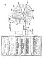
- FIG. 3depicts an actual and linear representation of a disk having defective segments and unusable segments corresponding to the defective segments according to an embodiment of the present invention
- FIG. 4depicts tracks which have defective segments and unusable segments corresponding to the defective segments according to an embodiment of the present invention
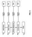
- FIG. 5is a process according to an embodiment of the present invention.
- FIG. 6depicts a defect management process according to an embodiment of the present invention
- FIG. 7depicts a defect margining process according to an embodiment of the present invention.
- FIG. 8depicts a defect margining process according to an embodiment of the present invention
- FIG. 9depicts tracks on a disk with defective segments according to an embodiment of the present invention.
- FIG. 10depicts tracks on a disk with multiple defective segments according to an embodiment of the present invention.
- FIG. 11depicts tracks on a disk with multiple defective segments and an unusable segment corresponding to a defective segment according to an embodiment of the present invention
- FIG. 12Adepicts a data storage device according to an embodiment of the present invention.
- FIG. 12Bdepicts a defect management process according to an embodiment of the present invention.
- a data storage device 100comprises a rotating magnetic disk 60 and a head 50 connected to the distal end of an actuator arm 25 .
- the actuator arm 25is rotated about a pivot by a voice coil motor (VCM) 20 to position the head 50 radially over the disk 60 .
- VCMvoice coil motor
- the data storage device 100also includes a spindle motor (not shown) for rotating the disk during read/write operations.
- the data storage device 100also comprises a controller 10 that performs various operations of the data storage device 100 described herein.
- the controller 10may be implemented using one or more processors for executing instructions and may further include memory, such as a volatile or non-volatile memory, for storing data (e.g., data being processed) and/or instructions.
- the instructionsmay be executed by the one or more processors to perform the various functions of the controller 10 described herein.
- the one or more processorsmay include a microcontroller, a Digital Signal Processor (DSP), an Application Specific Integrated Circuit (ASIC), a Field Programmable Gate Array (FPGA), hard-wired logic, analog circuitry and/or a combination thereof.
- DSPDigital Signal Processor
- ASICApplication Specific Integrated Circuit
- FPGAField Programmable Gate Array
- the disk 60comprises a number of radially spaced, concentric tracks 120 .
- Each track 120may be divided into a number of segments that are spaced circumferentially along the track 120 .
- the segmentsmay be used to store user data and other information.
- the segmentsare sectors or wedges.
- the disk 60may also comprise a plurality of angularly spaced servo wedges 22 0 - 22 N , each of which may include embedded servo information that can be read from the disk 60 by the head 50 to determine the position of the head 50 over the disk 60 .
- each servo wedge 22 0 - 22 Nmay include a pattern of alternating magnetic transitions (servo burst), which may be read from the disk 60 by the head 50 and processed by the controller 10 to estimate the position of the head 50 relative to the disk 60 .
- the angular spacing between the servo wedges 22 0 - 22 Nmay be uniform, as shown in the example in FIG. 1 .
- tracks 120 a - 120 d of the disk 60are formatted to form a user area, a relocation area, and an unused area.
- the disk 60includes 1.2 TB of usable space which can be divided such that the user area includes 1 TB of space, the relocation area includes 100 GB of space, and the unused area includes 100 GB of space.
- defective segments 122Prior to formatting the disk 60 , as seen in an embodiment in FIG. 3 , defective segments 122 , such as the defective segments 122 a and 122 b for the tracks 120 a - 120 d are detected by the controller 10 . Furthermore, the controller 10 can determine unusable segments, such as the unusable segments 124 a - 124 j corresponding to the defective segments 122 a and 122 b . In an embodiment, as seen in FIG. 4 , the defective segments 122 a and 122 b , and the unusable segments 124 a - 124 j reduce a usable space of the disk 60 from 1.2 TB to 0.8 TB.
- the defective segments 122 a and 122 b , and the unusable segments 124 a - 124 jexceed a maximum defective space amount.
- the disk 60may be unusable if, for example, 1 TB of usable space was required and only 0.8 TB of usable space was available.
- the controller 10performs a process to determine whether there is a capacity failure in the disk 60 .
- the controller 10performs a write scan process on the disk 60 . If during the write scan process the disk 60 does not have sufficient capacity, the disk fails and the controller 10 can transmit a storage capacity error signal to the test system.
- the controller 10performs a read scan process on the disk 60 . If during the read scan process the disk 60 does not have sufficient capacity, the disk 60 fails and the controller 10 can transmit the storage capacity error signal to the test system.
- the write scan process in Step 502 and the read scan process in Step 504are part of a defect management process, which will be described in more detail below.
- Step 506the controller 10 performs a defect margining process on the disk 60 , which will be described in more detail below. If during the defect margining process the disk 60 does not have sufficient capacity, the disk 60 fails and the controller 10 can transmit the storage capacity error signal to the test system.
- Step 508the controller 10 performs a formatting process on the disk 60 . If during the formatting process the disk 60 does not have sufficient capacity, the disk 60 fails and the controller 10 can transmit the storage capacity error signal to the test system. If the disk 60 passes the tests in Steps 502 - 508 , then the disk 60 passes and does not have a storage capacity error. In an embodiment, even if the disk fails, the controller 10 continues with the subsequent processes to provide failure analysis.
- the controlleris described as transmitting a storage capacity error signal to the test system upon detection of a capacity failure condition, in some embodiments the controller may perform other actions (e.g., storing an indication) in place of, or in addition to, sending the storage capacity error signal. In other embodiments, the controller may send different signal(s) to one or more systems.
- the controller 10performs a defect management process on the segments in the disk 60 as shown in FIG. 1B .
- the controller 10tests the plurality of segments for defects. For example, as shown in an embodiment in FIG. 9 , the controller 10 tests the segments in the tracks 120 a - 120 d.
- the controller 10detects a defect in a first segment of the plurality of segments.
- the controller 10can detect a defect in the defective segment 122 a as shown in FIG. 9 .
- the controller 10updates the defect list to include the first segment.
- the disk 60can store a defect list indicating segments of the plurality of segments which have defects.
- the controller 10can update the defect list to include the defective segment 122 a shown in an embodiment in FIG. 9 .
- the first segmentis the first detected defective segment by the controller 10 .
- the first segmentis a predetermined number of defective segments detected after a first detected defective segment by the controller 10 .
- the controller 10determines a defective space amount based on the segments in the updated defect list.
- the disk 60can store a defective space amount and the controller 10 can update the defective space amount based on an amount of space used by the segments in the updated defect list.
- the defective space amountis 33 GB, which reflects an amount of space used by the segments in the updated defect list including the defective segment 122 a .
- the defective space amountis stored in other locations aside from the disk 60 , such as a non-volatile memory or a volatile memory coupled to the controller 10 .
- the controller 10determines whether the defective space amount indicates a storage capacity error.
- the disk 60can store the maximum defective space amount, and the controller 10 can determine whether the defective space amount is greater than a maximum defective space amount.
- the maximum defective space amountis 100 GB and the defective space amount is 33 GB.
- the defective space amountis less than the maximum defective space amount.
- the maximum defective space amountis stored in other locations aside from the disk 60 , such as a memory coupled to the controller 10 .
- the controllerin some embodiments is described as determining whether the defective space amount is greater than a maximum defective space amount, other defective space determination methods may be used in some embodiments.
- the controllermay be configured to determine whether a remaining amount of non-defective (usable) space is below a minimum threshold amount.
- Step 112 in FIG. 1Bthe controller 10 transmits a storage capacity error signal to the test system when the defective space amount indicates the storage capacity error.
- the defective space amountis not greater than the maximum defective space amount, so the controller 10 would not transmit the storage capacity error signal to the test system. However, if the defective space amount was greater than the maximum defective space amount, the controller 10 would transmit the storage capacity error to the test system.
- Step 114 in FIG. 1Bwhen the defective space amount does not indicate the storage capacity error, the controller 10 continues to test the plurality of segments for defects until the defective space amount indicates the storage capacity error or all of the plurality of segments have been tested. For example, when the defective space amount is not greater than the maximum defective space amount, the controller 10 can continue to test the remaining untested segments in the disk 60 until the defective space amount is greater than the maximum defective space amount or all of the segments have been tested. Otherwise, if the defective space amount is greater than the maximum defective space amount, the controller 10 will not continue to test the plurality of segments in the disk 60 .
- the defect management processfurther includes the process disclosed in FIG. 6 .
- the controller 10detects a defect in a second segment.
- the controller 10detects a defect in the defective segment 122 b .
- the second segmentis a first defective segment after the first segment.
- the second segmentis a predetermined number of detected defective segments after the first segment in the defect list.
- the second segmentcan be one or more defective segments detected by the controller 10 after the first segment.
- the controller 10updates the defect list to include the second segment. For example, the controller 10 can update the defect list to include the defective segment 122 b .
- the controller 10determines the defective space amount based on the segments in the updated defect list. For example, the controller 10 can determine the defective space amount based on the amount of space used by the segments in the updated defect list. In an embodiment, as seen in FIG. 10 , the defective space amount is 66 GB, which reflects an amount of space used by the segments in the updated defect list including the defective segment 122 b in addition to the defective segment 122 a.
- Step 608 in FIG. 6the controller 10 determines whether the defective space amount indicates the storage capacity error.
- the maximum defective space amountis 100 GB and the defective space amount is 66 GB. Thus, the defective space amount is not greater than the maximum defective space amount.
- Step 610 in FIG. 6the controller 10 transmits the storage capacity error signal to the test system when the defective space amount indicates the storage capacity error.
- the controller 10would not transmit the storage capacity error signal to the test system because the defective space amount is not greater than the maximum defective space amount.
- Step 612 in FIG. 6when the defective space amount does not indicate the storage capacity error, the controller 10 continues to test the plurality of segments for defects until the defective space amount indicates the storage capacity error or all of the plurality of segments have been tested. Otherwise, if the defective space amount does indicate the storage capacity error, the controller 10 will not continue to test the plurality of segments in the disk 60 .
- the controller 10performs a defect margining process on the plurality of segments in the disk 60 as shown in FIG. 7 . In an embodiment, the controller 10 performs the defect margining process after determining that there is no storage capacity error based on the defective space amount when performing the defect management process.
- the controller 10determines unusable segments corresponding to the first segment in the defect list. For example, in an embodiment seen in FIG. 11 , the controller 10 determines unusable segments such as the unusable segment 124 a corresponding to the defective segment 122 a .
- the first segmentis a first defective segment in the defect list.
- the first segmentis a predetermined number of defective segments after a first defective segment in the defect list.
- the unusable segments corresponding to the first segmentare added to the defect list.
- the unusable segments corresponding to the first segmentare added to another list different from the defect list.
- the unusable segmentscould be determined for not just the first segment, but a first cluster of segments including the first segment and other defective segments in the defect list located near each other.
- unusable segments 124 a - 124 jcould be determined for a cluster of segments including the defective segments 122 a and 122 b as shown in FIG. 3 .
- the controller 10updates the defective space amount based on the unusable segments corresponding to the first segment.
- the controller 10can update the defective space amount based on an amount of space used by the unusable segments such as the unusable segment 124 a corresponding to the defective segment 122 a .
- the defective space amountis 166 GB, which reflects an amount of space used by the segments in the updated defect list including the unusable segment 124 a in addition to the defective segments 122 a and 122 b .
- the defective space amountis updated based on not just a single unusable segment, but a plurality of unusable segments near each other.
- the defective space amountcan be updated based on not just the segment 124 a but additional segments near the segment 124 a such as the segments 124 e and 124 i ( FIG. 3 ).
- Step 706 in FIG. 7the controller 10 determines whether the defective space amount indicates the storage capacity error.
- the maximum defective space amountis 100 GB and the defective space amount is 166 GB. Thus, the defective space amount is greater than the maximum defective space amount.
- Step 708 in FIG. 7the controller 10 transmits the storage capacity error signal to the test system when the defective space amount indicates the storage capacity error.
- the controller 10transmits the storage capacity error signal to the test system because the defective space amount is greater than the maximum defective space amount. However, if the defective space amount is not greater than the maximum defective space amount, then the controller 10 would not transmit the storage capacity error signal to the test system.
- Step 710 in FIG. 7when the defective space amount does not indicate the storage capacity error, the controller 10 continues to determine unusable segments corresponding to segments in the defect list until the defective space amount indicates the storage capacity error or all of the unusable segments corresponding to segments in the defect list have been determined. In an embodiment, in FIG. 11 , the controller 10 would not continue to determine unusable segments corresponding to segments in the defect list because the defective space amount is greater than the maximum defective space amount. However, if the defective space amount was less than the maximum defective space amount, the controller 10 would continue to determine unusable segments corresponding to segments in the defect list until the defective space amount is greater than the maximum defective space amount or all of the unusable segments corresponding to segments in the defect list have been determined.
- the defect margining process performed by the controller 10further includes the process shown in FIG. 8 .
- the controller 10determines unusable segments corresponding to the second segment in the defect list. For example, if the defective space amount is not greater than the maximum defective space amount after determining the unusable segments corresponding to the defective segment 122 a , the controller 10 can determine unusable segments corresponding to the defective segment 122 b in FIGS. 3 and 4 .
- the second segmentis a first defective segment after the first segment in the defect list.
- the second segmentis a predetermined number of defective segments after the first segment in the defect list.
- the unusable segments corresponding to the second segmentare added to the defect list.
- the unusable segments corresponding to the second segmentare added to another list different from the defect list.
- the unusable segmentscould be determined for not just the second segment, but a second cluster of segments including the second segment and other defective segments in the defect list located near each other.
- unusable segments 124 a - 124 jcould be determined for a cluster of segments including the defective segments 122 a and 122 b as shown in FIG. 3 .
- the controller 10updates the defective space amount based on the unusable segments corresponding to the second segment.
- the controller 10can update the defective space amount based on an amount of space used by the unusable segments corresponding to the defective segment 122 b .
- the defective space amountis updated based on not just a single unusable segment, but a plurality of unusable segments near each other.
- Step 806the controller 10 determines whether the defective space amount indicates the storage capacity error.
- Step 808the controller 10 transmits the storage capacity error signal to the test system when the defective space amount indicates the storage capacity error.
- Step 810when the defective space amount does not indicate the storage capacity error, the controller 10 continues to determine unusable segments corresponding to segments in the defect list until the defective space amount indicates the storage capacity error or all of the unusable segments corresponding to segments in the defect list have been determined. For example, when the defective space amount is not greater than the maximum defective space amount, the controller 10 can continue to determine unusable segments corresponding to segments in the defect list until the defective space amount is greater than the maximum defective space amount or all of the unusable segments corresponding to segments in the defect list have been determined.
- the controller 10also performs a formatting process on a non-volatile media after determining that there is no storage capacity error based on the defective space amount when performing the defect management process and the defect margining process disclosed above. Furthermore, the controller 10 can be configured to determine when there is a storage capacity error based on the defect space amount during the formatting process on the non-volatile media.
- the controller 10determines whether the defective space amount indicates the storage capacity error using a usable space amount instead of the maximum defective space amount. For example, the controller 10 can determine the usable space amount using the defective space amount and compare the usable space amount to a minimum usable space amount to determine if there is sufficient space in the disk 60 . When the usable space amount is greater than the minimum usable space amount, there is sufficient space in the disk 60 and there is no storage capacity error. However, when the usable space amount is not greater than the minimum usable space amount, then there is the storage capacity error for the disk 60 .
- a non-volatile media 160is seen in a data storage device 900 .
- the non-volatile media 160 in FIG. 12Aincludes the disk 60 or a non-volatile semiconductor memory, e.g., NAND flash memory.
- the non-volatile media 160includes both the disk 60 and the non-volatile semiconductor memory.
- the data storage device 900is similar to the data storage device 100 except for the inclusion of the non-volatile media 160 , and thus further description will be omitted.
- the process shown in FIG. 12Bis similar to the process in FIG. 1B and the description will not be repeated.
- a software modulemay reside in RAM memory, flash memory, ROM memory, EPROM memory, EEPROM memory, registers, hard disk, a removable disk, a CD-ROM, or any other form of storage medium known in the art.
- An exemplary storage mediumis coupled to the processor such that the processor can read information from, and write information to, the storage medium.
- the storage mediummay be integral to the processor.
- the processor and the storage mediummay reside in an Application Specific Integrated Circuit (ASIC).
- the ASICmay reside in a wireless modem.
- the processor and the storage mediummay reside as discrete components in the wireless modem.
Landscapes
- Engineering & Computer Science (AREA)
- Signal Processing (AREA)
- Debugging And Monitoring (AREA)
Abstract
Description
Claims (38)
Priority Applications (1)
| Application Number | Priority Date | Filing Date | Title |
|---|---|---|---|
| US13/282,274US8711665B1 (en) | 2011-10-26 | 2011-10-26 | Method and apparatus for determining storage capacity error for a data storage device |
Applications Claiming Priority (1)
| Application Number | Priority Date | Filing Date | Title |
|---|---|---|---|
| US13/282,274US8711665B1 (en) | 2011-10-26 | 2011-10-26 | Method and apparatus for determining storage capacity error for a data storage device |
Publications (1)
| Publication Number | Publication Date |
|---|---|
| US8711665B1true US8711665B1 (en) | 2014-04-29 |
Family
ID=50514269
Family Applications (1)
| Application Number | Title | Priority Date | Filing Date |
|---|---|---|---|
| US13/282,274Active2032-06-06US8711665B1 (en) | 2011-10-26 | 2011-10-26 | Method and apparatus for determining storage capacity error for a data storage device |
Country Status (1)
| Country | Link |
|---|---|
| US (1) | US8711665B1 (en) |
Cited By (81)
| Publication number | Priority date | Publication date | Assignee | Title |
|---|---|---|---|---|
| US8891193B1 (en) | 2013-05-09 | 2014-11-18 | Western Digital Technologies, Inc. | Disk drive calibrating threshold and gain of touchdown sensor |
| US8891341B1 (en) | 2013-03-11 | 2014-11-18 | Western Digital Technologies, Inc. | Energy assisted magnetic recording disk drive using modulated laser light |
| US8941941B1 (en) | 2013-02-28 | 2015-01-27 | Western Digital Technologies, Inc. | Disk drive calibrating touchdown sensor |
| US8947812B1 (en) | 2014-03-27 | 2015-02-03 | Western Digital Technologies, Inc. | Data storage device comprising equalizer filter and inter-track interference filter |
| US8953277B1 (en) | 2014-06-16 | 2015-02-10 | Western Digital Technologies, Inc. | Data storage device writing tracks on a disk with equal spacing |
| US8958167B1 (en) | 2013-12-23 | 2015-02-17 | Western Digital Technologies, Inc. | Detection of disk surface irregularities in data storage devices |
| US8970978B1 (en) | 2012-10-22 | 2015-03-03 | Western Digital Technologies, Inc. | Disk drive detecting head touchdown by applying DC+AC control signal to fly height actuator |
| US8976633B1 (en) | 2014-04-15 | 2015-03-10 | Western Digital Technologies, Inc. | Data storage device calibrating fly height actuator based on laser power for heat assisted magnetic recording |
| US8988810B1 (en) | 2014-04-16 | 2015-03-24 | Western Digital Technologies, Inc. | Track measurement for data storage device |
| US8988809B1 (en) | 2014-02-18 | 2015-03-24 | Western Digital (Fremont), Llc | Disk recording device for writing a radially coherent reference band by measuring relative timing offsets of reference bursts |
| US9001453B1 (en) | 2014-07-18 | 2015-04-07 | Western Digital Technologies, Inc. | Data storage device calibrating fly height actuator based on read mode touchdown resistance of touchdown sensor |
| US9013818B1 (en) | 2013-12-06 | 2015-04-21 | Western Digital Technologies, Inc. | Disk drive measuring reader/writer gap by measuring fractional clock cycle over disk radius |
| US9013821B1 (en) | 2014-06-10 | 2015-04-21 | Western Digital Technologies, Inc. | Data storage device employing one-dimensional and two-dimensional channels |
| US9025267B1 (en) | 2014-06-09 | 2015-05-05 | Western Digital Technologies, Inc. | Data storage device using branch metric from adjacent track to compensate for inter-track interference |
| US9025421B1 (en) | 2014-10-08 | 2015-05-05 | Western Digital Technologies, Inc. | Data storage device adjusting laser input power to compensate for temperature variations |
| US9047917B1 (en) | 2013-11-26 | 2015-06-02 | Western Digital Technologies, Inc. | Disk drive slider with sense amplifier for coupling to a preamp through a supply/bias line and a read signal line |
| US9053749B1 (en) | 2013-03-15 | 2015-06-09 | Western Digital Technologies, Inc. | Disk drive comprising a per-drive and per-head fly height filter |
| US9053730B1 (en) | 2012-05-11 | 2015-06-09 | Western Digital Technologies, Inc. | Disk drive comprising extended range head proximity sensor |
| US9064525B2 (en) | 2013-11-26 | 2015-06-23 | Western Digital Technologies, Inc. | Disk drive comprising laser transmission line optimized for heat assisted magnetic recording |
| US9070406B1 (en) | 2014-03-10 | 2015-06-30 | Western Digital Technologies, Inc. | Disk drive configuring one-dimensional and two-dimensional recording areas based on read element spacing |
| US9076474B1 (en) | 2014-12-23 | 2015-07-07 | Western Digital Technologies, Inc. | Data storage device attenuating thermal decay effect on fly height measurement |
| US9074941B1 (en) | 2013-03-14 | 2015-07-07 | Western Digital Technologies, Inc. | Systems and methods for measuring ambient and laser temperature in heat assisted magnetic recording |
| US9082458B1 (en) | 2014-03-10 | 2015-07-14 | Western Digital Technologies, Inc. | Data storage device balancing and maximizing quality metric when configuring arial density of each disk surface |
| US9099134B1 (en) | 2015-01-27 | 2015-08-04 | Western Digital Technologies, Inc. | Data storage device employing multiple jog profiles for a butterfly written disk surface |
| US9099103B1 (en) | 2014-10-21 | 2015-08-04 | Western Digital Technologies, Inc. | Heat assisted magnetic recording withinterlaced high-power heated and low-power heated tracks |
| US9099144B1 (en) | 2013-10-11 | 2015-08-04 | Western Digital Technologies, Inc. | Disk drive evaluating laser performance for heat assisted magnetic recording |
| US9117489B1 (en) | 2014-02-18 | 2015-08-25 | Western Digital Technologies, Inc. | Data storage device screening heads by verifying defects after defect scan |
| US9117479B1 (en) | 2014-09-24 | 2015-08-25 | Western Digital Technologies, Inc. | Data storage device calibrating laser write power for heat assisted magnetic recording |
| US9117463B1 (en) | 2014-06-23 | 2015-08-25 | Western Digital Technologies, Inc. | Data storage device erasing multiple adjacent data tracks to recover from inter-track interference |
| US9123370B1 (en) | 2014-04-15 | 2015-09-01 | Western Digital Technologies, Inc. | Data storage device calibrating fly height actuator based on laser power for heat assisted magnetic recording |
| US9153266B1 (en) | 2014-09-11 | 2015-10-06 | Western Digital Technologies, Inc. | Data storage device measuring laser protrusion fly height profile |
| US9171575B1 (en) | 2014-06-23 | 2015-10-27 | Western Digital Technologies, Inc. | Data storage device detecting media defects by writing opposite polarity test pattern |
| US9183877B1 (en) | 2015-03-20 | 2015-11-10 | Western Digital Technologies, Inc. | Data storage device comprising two-dimensional data dependent noise whitening filters for two-dimensional recording |
| US20150347039A1 (en)* | 2014-05-30 | 2015-12-03 | Sandisk Enterprise Ip Llc | Method and System for Recharacterizing the Storage Density of a Memory Device or a Portion Thereof |
| US9214186B1 (en) | 2015-03-23 | 2015-12-15 | Western Digital Technologies, Inc. | Data storage device measuring radial offset between read element and write element |
| US9213493B1 (en) | 2011-12-16 | 2015-12-15 | Western Digital Technologies, Inc. | Sorted serpentine mapping for storage drives |
| US9230605B1 (en) | 2014-12-01 | 2016-01-05 | Western Digital Technologies, Inc. | Data storage device maximizing areal density based on a target quality metric |
| US9230585B1 (en) | 2014-01-31 | 2016-01-05 | Western Digital Technologies, Inc. | Per wedge preheat DFH to improve data storage device performance |
| US9245556B2 (en) | 2014-03-10 | 2016-01-26 | Western Digital Technologies, Inc. | Disk drive employing multiple read elements to increase radial band for two-dimensional magnetic recording |
| US9251856B1 (en) | 2014-05-30 | 2016-02-02 | Western Digial Technologies, Inc. | Read failover method and apparatus for a data storage system |
| US9251844B1 (en) | 2014-06-02 | 2016-02-02 | Western Digital Technologies, Inc. | Waterfall method and apparatus for a data storage device read system |
| US9257146B1 (en) | 2014-02-11 | 2016-02-09 | Western Digital Technologies, Inc. | Data storage device comprising sequence detector compensating for inter-track interference |
| US9257145B1 (en) | 2013-11-27 | 2016-02-09 | Western Digital Technologies, Inc. | Disk drive measuring down-track spacing of read sensors |
| US9281009B1 (en) | 2014-12-18 | 2016-03-08 | Western Digital Technologies, Inc. | Data storage device employing variable size interleave written track segments |
| US9286150B2 (en) | 2013-09-16 | 2016-03-15 | Seagate Technology Llc | Dynamic band boundaries |
| US9318137B1 (en) | 2015-03-13 | 2016-04-19 | Western Digital Technologies, Inc. | Data storage device executing retry operation by buffering signal samples at different radial offsets |
| US9355666B1 (en) | 2013-09-30 | 2016-05-31 | Western Digital Technologies, Inc. | Disk drive measuring stroke difference between heads by detecting a difference between ramp contact |
| US9361938B1 (en) | 2015-04-16 | 2016-06-07 | Western Digital Technologies, Inc. | Disk defect management for a data storage device |
| US9368132B1 (en) | 2015-09-04 | 2016-06-14 | Western Digital Technologies, Inc. | Data storage device employing differential write data signal and differential write pattern signal |
| US9368131B1 (en) | 2015-04-03 | 2016-06-14 | Western Digital (Fremont), Llc | Data storage device employing mirrored cross-track profiles for top and bottom disk surfaces |
| US9401165B1 (en) | 2014-05-05 | 2016-07-26 | Western Digital Technologies, Inc. | Method and system to monitor magnetic head loading and unloading stability for a data storage system |
| US9417628B2 (en) | 2013-03-13 | 2016-08-16 | Western Digital Technologies, Inc. | Production failure analysis system |
| US9442670B2 (en) | 2013-09-03 | 2016-09-13 | Sandisk Technologies Llc | Method and system for rebalancing data stored in flash memory devices |
| US9460751B2 (en)* | 2013-09-16 | 2016-10-04 | Seagate Technology Llc | Binding shingled recording bands |
| US9472219B1 (en) | 2015-05-01 | 2016-10-18 | Western Digital Technologies, Inc. | Data storage device calibrating parameter for heat assisted magnetic recording |
| US9502068B1 (en) | 2015-04-08 | 2016-11-22 | Western Digital Technologies, Inc. | Data storage device updating laser power during non-write mode for heat assisted magnetic recording |
| US9519427B2 (en) | 2014-09-02 | 2016-12-13 | Sandisk Technologies Llc | Triggering, at a host system, a process to reduce declared capacity of a storage device |
| US9519577B2 (en) | 2013-09-03 | 2016-12-13 | Sandisk Technologies Llc | Method and system for migrating data between flash memory devices |
| US9524112B2 (en) | 2014-09-02 | 2016-12-20 | Sandisk Technologies Llc | Process and apparatus to reduce declared capacity of a storage device by trimming |
| US9524105B2 (en) | 2014-09-02 | 2016-12-20 | Sandisk Technologies Llc | Process and apparatus to reduce declared capacity of a storage device by altering an encoding format |
| US9552166B2 (en) | 2014-09-02 | 2017-01-24 | Sandisk Technologies Llc. | Process and apparatus to reduce declared capacity of a storage device by deleting data |
| US9563362B2 (en) | 2014-09-02 | 2017-02-07 | Sandisk Technologies Llc | Host system and process to reduce declared capacity of a storage device by trimming |
| US9563370B2 (en) | 2014-09-02 | 2017-02-07 | Sandisk Technologies Llc | Triggering a process to reduce declared capacity of a storage device |
| US9582193B2 (en) | 2014-09-02 | 2017-02-28 | Sandisk Technologies Llc | Triggering a process to reduce declared capacity of a storage device in a multi-storage-device storage system |
| US9582202B2 (en) | 2014-09-02 | 2017-02-28 | Sandisk Technologies Llc | Process and apparatus to reduce declared capacity of a storage device by moving data |
| US9582203B2 (en) | 2014-09-02 | 2017-02-28 | Sandisk Technologies Llc | Process and apparatus to reduce declared capacity of a storage device by reducing a range of logical addresses |
| US9582212B2 (en) | 2014-09-02 | 2017-02-28 | Sandisk Technologies Llc | Notification of trigger condition to reduce declared capacity of a storage device |
| US9582220B2 (en) | 2014-09-02 | 2017-02-28 | Sandisk Technologies Llc | Notification of trigger condition to reduce declared capacity of a storage device in a multi-storage-device storage system |
| US9606737B2 (en) | 2015-05-20 | 2017-03-28 | Sandisk Technologies Llc | Variable bit encoding per NAND flash cell to extend life of flash-based storage devices and preserve over-provisioning |
| US9652153B2 (en) | 2014-09-02 | 2017-05-16 | Sandisk Technologies Llc | Process and apparatus to reduce declared capacity of a storage device by reducing a count of logical addresses |
| US9665311B2 (en) | 2014-09-02 | 2017-05-30 | Sandisk Technologies Llc | Process and apparatus to reduce declared capacity of a storage device by making specific logical addresses unavailable |
| US9747928B1 (en) | 2014-09-25 | 2017-08-29 | Western Digital Technologies, Inc. | Data storage device modifying write operation when a laser mode hop is detected |
| US9761273B1 (en) | 2015-11-03 | 2017-09-12 | Western Digital Technologies, Inc. | Data storage device encoding and interleaving codewords to improve trellis sequence detection |
| US9842617B1 (en) | 2015-06-29 | 2017-12-12 | Western Digital Technologies, Inc. | Electronic system with head management mechanism and method of operation thereof |
| US9891844B2 (en) | 2015-05-20 | 2018-02-13 | Sandisk Technologies Llc | Variable bit encoding per NAND flash cell to improve device endurance and extend life of flash-based storage devices |
| US9898364B2 (en) | 2014-05-30 | 2018-02-20 | Sandisk Technologies Llc | Method and system for dynamic word line based configuration of a three-dimensional memory device |
| US9916616B2 (en) | 2014-03-31 | 2018-03-13 | Western Digital Technologies, Inc. | Inventory management system using incremental capacity formats |
| US9946473B2 (en) | 2015-12-03 | 2018-04-17 | Sandisk Technologies Llc | Efficiently managing unmapped blocks to extend life of solid state drive |
| US9946483B2 (en) | 2015-12-03 | 2018-04-17 | Sandisk Technologies Llc | Efficiently managing unmapped blocks to extend life of solid state drive with low over-provisioning |
| US10056920B1 (en) | 2015-11-03 | 2018-08-21 | Western Digital Technologies, Inc. | Data storage device encoding and interleaving codewords to improve trellis sequence detection |
| US10063257B1 (en) | 2015-11-03 | 2018-08-28 | Western Digital Technologies, Inc. | Data storage device encoding and interleaving codewords to improve trellis sequence detection |
Citations (19)
| Publication number | Priority date | Publication date | Assignee | Title |
|---|---|---|---|---|
| US5917724A (en) | 1997-12-20 | 1999-06-29 | Ncr Corporation | Method for predicting disk drive failure by monitoring the rate of growth of defects within a disk drive |
| US6034831A (en) | 1997-05-09 | 2000-03-07 | International Business Machines Corporation | Dynamic reverse reassign apparatus and method for a data recording disk drive |
| US6078452A (en) | 1998-06-22 | 2000-06-20 | Western Digital Corporation | Disk drive employing method of writing a data block to a data sector following a defective servo sector |
| US6204660B1 (en) | 1997-06-03 | 2001-03-20 | Samsung Electronics Co., Ltd. | Method of varying capacity of head disk drive during manufacturing process by checking head/disk combinations for defects |
| US6223303B1 (en) | 1998-06-29 | 2001-04-24 | Western Digital Corporation | Disk drive having two tiered defect list comprising marginal and reserved data sectors |
| US6408406B1 (en) | 1999-08-31 | 2002-06-18 | Western Digital Technologies, Inc. | Hard disk drive infant mortality test |
| US20020191319A1 (en)* | 2001-04-12 | 2002-12-19 | Seagate Technology Llc | Merged defect entries for defects running in circumferential and radial directions on a disc |
| US6563776B1 (en) | 1998-07-10 | 2003-05-13 | Fujitsu Limited | Information storage apparatus for monitoring a number of defective sectors included in a zone so as to select a substitutional area from a different zone |
| US6717758B2 (en) | 2001-05-15 | 2004-04-06 | Iomega Corporation | Disk partitioning to create a usable, lower capacity disk cartridge |
| US20040158769A1 (en) | 2002-12-12 | 2004-08-12 | Samsung Electronics Co., Ltd. | Apparatus and method for managing random-directional scratches on hard disk |
| US6985319B2 (en) | 2000-05-22 | 2006-01-10 | Seagate Technology Llc | Pattern-based defect description method |
| US20060056088A1 (en) | 2004-09-15 | 2006-03-16 | Hitachi Global Storage Technologies Netherlands B.V. | Defect registration method of magnetic disk, and magnetic disk drive |
| US7072129B1 (en)* | 2004-06-30 | 2006-07-04 | Western Digital Technologies, Inc. | Identifying defective data sectors in a disk drive |
| US7139145B1 (en) | 2004-09-23 | 2006-11-21 | Western Digital Technologies, Inc. | Cluster-based defect detection testing for disk drives |
| US20070146921A1 (en) | 2005-12-27 | 2007-06-28 | Jun Jin-Wan | Hard disk drive and method for managing scratches on a disk of the hard disk drive |
| US7245445B2 (en) | 2002-11-25 | 2007-07-17 | Samsung Electronics Co., Ltd. | Method of managing defects in hard disk drive, recording media therefor and hard disk drive therefor |
| US20080270675A1 (en)* | 2007-04-25 | 2008-10-30 | Dheemanth Nagaraj | Defect management for a semiconductor memory system |
| US20100315916A1 (en)* | 2009-05-11 | 2010-12-16 | Panasonic Corporation | Information recording medium, information recording method, information recording apparatus, information reproducing method and information reproducing apparatus |
| US8054717B1 (en) | 2006-10-16 | 2011-11-08 | Marvell International Ltd. | Defect detection design |
- 2011
- 2011-10-26USUS13/282,274patent/US8711665B1/enactiveActive
Patent Citations (19)
| Publication number | Priority date | Publication date | Assignee | Title |
|---|---|---|---|---|
| US6034831A (en) | 1997-05-09 | 2000-03-07 | International Business Machines Corporation | Dynamic reverse reassign apparatus and method for a data recording disk drive |
| US6204660B1 (en) | 1997-06-03 | 2001-03-20 | Samsung Electronics Co., Ltd. | Method of varying capacity of head disk drive during manufacturing process by checking head/disk combinations for defects |
| US5917724A (en) | 1997-12-20 | 1999-06-29 | Ncr Corporation | Method for predicting disk drive failure by monitoring the rate of growth of defects within a disk drive |
| US6078452A (en) | 1998-06-22 | 2000-06-20 | Western Digital Corporation | Disk drive employing method of writing a data block to a data sector following a defective servo sector |
| US6223303B1 (en) | 1998-06-29 | 2001-04-24 | Western Digital Corporation | Disk drive having two tiered defect list comprising marginal and reserved data sectors |
| US6563776B1 (en) | 1998-07-10 | 2003-05-13 | Fujitsu Limited | Information storage apparatus for monitoring a number of defective sectors included in a zone so as to select a substitutional area from a different zone |
| US6408406B1 (en) | 1999-08-31 | 2002-06-18 | Western Digital Technologies, Inc. | Hard disk drive infant mortality test |
| US6985319B2 (en) | 2000-05-22 | 2006-01-10 | Seagate Technology Llc | Pattern-based defect description method |
| US20020191319A1 (en)* | 2001-04-12 | 2002-12-19 | Seagate Technology Llc | Merged defect entries for defects running in circumferential and radial directions on a disc |
| US6717758B2 (en) | 2001-05-15 | 2004-04-06 | Iomega Corporation | Disk partitioning to create a usable, lower capacity disk cartridge |
| US7245445B2 (en) | 2002-11-25 | 2007-07-17 | Samsung Electronics Co., Ltd. | Method of managing defects in hard disk drive, recording media therefor and hard disk drive therefor |
| US20040158769A1 (en) | 2002-12-12 | 2004-08-12 | Samsung Electronics Co., Ltd. | Apparatus and method for managing random-directional scratches on hard disk |
| US7072129B1 (en)* | 2004-06-30 | 2006-07-04 | Western Digital Technologies, Inc. | Identifying defective data sectors in a disk drive |
| US20060056088A1 (en) | 2004-09-15 | 2006-03-16 | Hitachi Global Storage Technologies Netherlands B.V. | Defect registration method of magnetic disk, and magnetic disk drive |
| US7139145B1 (en) | 2004-09-23 | 2006-11-21 | Western Digital Technologies, Inc. | Cluster-based defect detection testing for disk drives |
| US20070146921A1 (en) | 2005-12-27 | 2007-06-28 | Jun Jin-Wan | Hard disk drive and method for managing scratches on a disk of the hard disk drive |
| US8054717B1 (en) | 2006-10-16 | 2011-11-08 | Marvell International Ltd. | Defect detection design |
| US20080270675A1 (en)* | 2007-04-25 | 2008-10-30 | Dheemanth Nagaraj | Defect management for a semiconductor memory system |
| US20100315916A1 (en)* | 2009-05-11 | 2010-12-16 | Panasonic Corporation | Information recording medium, information recording method, information recording apparatus, information reproducing method and information reproducing apparatus |
Cited By (88)
| Publication number | Priority date | Publication date | Assignee | Title |
|---|---|---|---|---|
| US9213493B1 (en) | 2011-12-16 | 2015-12-15 | Western Digital Technologies, Inc. | Sorted serpentine mapping for storage drives |
| US9053730B1 (en) | 2012-05-11 | 2015-06-09 | Western Digital Technologies, Inc. | Disk drive comprising extended range head proximity sensor |
| US8970978B1 (en) | 2012-10-22 | 2015-03-03 | Western Digital Technologies, Inc. | Disk drive detecting head touchdown by applying DC+AC control signal to fly height actuator |
| US8941941B1 (en) | 2013-02-28 | 2015-01-27 | Western Digital Technologies, Inc. | Disk drive calibrating touchdown sensor |
| US8891341B1 (en) | 2013-03-11 | 2014-11-18 | Western Digital Technologies, Inc. | Energy assisted magnetic recording disk drive using modulated laser light |
| US9417628B2 (en) | 2013-03-13 | 2016-08-16 | Western Digital Technologies, Inc. | Production failure analysis system |
| US9074941B1 (en) | 2013-03-14 | 2015-07-07 | Western Digital Technologies, Inc. | Systems and methods for measuring ambient and laser temperature in heat assisted magnetic recording |
| US9053749B1 (en) | 2013-03-15 | 2015-06-09 | Western Digital Technologies, Inc. | Disk drive comprising a per-drive and per-head fly height filter |
| US8891193B1 (en) | 2013-05-09 | 2014-11-18 | Western Digital Technologies, Inc. | Disk drive calibrating threshold and gain of touchdown sensor |
| US9442670B2 (en) | 2013-09-03 | 2016-09-13 | Sandisk Technologies Llc | Method and system for rebalancing data stored in flash memory devices |
| US9519577B2 (en) | 2013-09-03 | 2016-12-13 | Sandisk Technologies Llc | Method and system for migrating data between flash memory devices |
| US9460751B2 (en)* | 2013-09-16 | 2016-10-04 | Seagate Technology Llc | Binding shingled recording bands |
| US9286150B2 (en) | 2013-09-16 | 2016-03-15 | Seagate Technology Llc | Dynamic band boundaries |
| US9355666B1 (en) | 2013-09-30 | 2016-05-31 | Western Digital Technologies, Inc. | Disk drive measuring stroke difference between heads by detecting a difference between ramp contact |
| US9099144B1 (en) | 2013-10-11 | 2015-08-04 | Western Digital Technologies, Inc. | Disk drive evaluating laser performance for heat assisted magnetic recording |
| US9299371B1 (en) | 2013-11-26 | 2016-03-29 | Western Digital Technologies, Inc. | Disk drive slider with sense amplifier for coupling to a preamp through a supply/bias line and a read signal line |
| US9047917B1 (en) | 2013-11-26 | 2015-06-02 | Western Digital Technologies, Inc. | Disk drive slider with sense amplifier for coupling to a preamp through a supply/bias line and a read signal line |
| US9064525B2 (en) | 2013-11-26 | 2015-06-23 | Western Digital Technologies, Inc. | Disk drive comprising laser transmission line optimized for heat assisted magnetic recording |
| US9257145B1 (en) | 2013-11-27 | 2016-02-09 | Western Digital Technologies, Inc. | Disk drive measuring down-track spacing of read sensors |
| US9013818B1 (en) | 2013-12-06 | 2015-04-21 | Western Digital Technologies, Inc. | Disk drive measuring reader/writer gap by measuring fractional clock cycle over disk radius |
| US8958167B1 (en) | 2013-12-23 | 2015-02-17 | Western Digital Technologies, Inc. | Detection of disk surface irregularities in data storage devices |
| US9230585B1 (en) | 2014-01-31 | 2016-01-05 | Western Digital Technologies, Inc. | Per wedge preheat DFH to improve data storage device performance |
| US9257146B1 (en) | 2014-02-11 | 2016-02-09 | Western Digital Technologies, Inc. | Data storage device comprising sequence detector compensating for inter-track interference |
| US8988809B1 (en) | 2014-02-18 | 2015-03-24 | Western Digital (Fremont), Llc | Disk recording device for writing a radially coherent reference band by measuring relative timing offsets of reference bursts |
| US9117489B1 (en) | 2014-02-18 | 2015-08-25 | Western Digital Technologies, Inc. | Data storage device screening heads by verifying defects after defect scan |
| US9082458B1 (en) | 2014-03-10 | 2015-07-14 | Western Digital Technologies, Inc. | Data storage device balancing and maximizing quality metric when configuring arial density of each disk surface |
| US9245556B2 (en) | 2014-03-10 | 2016-01-26 | Western Digital Technologies, Inc. | Disk drive employing multiple read elements to increase radial band for two-dimensional magnetic recording |
| US9070406B1 (en) | 2014-03-10 | 2015-06-30 | Western Digital Technologies, Inc. | Disk drive configuring one-dimensional and two-dimensional recording areas based on read element spacing |
| US8947812B1 (en) | 2014-03-27 | 2015-02-03 | Western Digital Technologies, Inc. | Data storage device comprising equalizer filter and inter-track interference filter |
| US9916616B2 (en) | 2014-03-31 | 2018-03-13 | Western Digital Technologies, Inc. | Inventory management system using incremental capacity formats |
| US8976633B1 (en) | 2014-04-15 | 2015-03-10 | Western Digital Technologies, Inc. | Data storage device calibrating fly height actuator based on laser power for heat assisted magnetic recording |
| US9123370B1 (en) | 2014-04-15 | 2015-09-01 | Western Digital Technologies, Inc. | Data storage device calibrating fly height actuator based on laser power for heat assisted magnetic recording |
| US8988810B1 (en) | 2014-04-16 | 2015-03-24 | Western Digital Technologies, Inc. | Track measurement for data storage device |
| US9401165B1 (en) | 2014-05-05 | 2016-07-26 | Western Digital Technologies, Inc. | Method and system to monitor magnetic head loading and unloading stability for a data storage system |
| US20150347039A1 (en)* | 2014-05-30 | 2015-12-03 | Sandisk Enterprise Ip Llc | Method and System for Recharacterizing the Storage Density of a Memory Device or a Portion Thereof |
| US9645749B2 (en)* | 2014-05-30 | 2017-05-09 | Sandisk Technologies Llc | Method and system for recharacterizing the storage density of a memory device or a portion thereof |
| US9251856B1 (en) | 2014-05-30 | 2016-02-02 | Western Digial Technologies, Inc. | Read failover method and apparatus for a data storage system |
| US9898364B2 (en) | 2014-05-30 | 2018-02-20 | Sandisk Technologies Llc | Method and system for dynamic word line based configuration of a three-dimensional memory device |
| US9251844B1 (en) | 2014-06-02 | 2016-02-02 | Western Digital Technologies, Inc. | Waterfall method and apparatus for a data storage device read system |
| US9025267B1 (en) | 2014-06-09 | 2015-05-05 | Western Digital Technologies, Inc. | Data storage device using branch metric from adjacent track to compensate for inter-track interference |
| US9013821B1 (en) | 2014-06-10 | 2015-04-21 | Western Digital Technologies, Inc. | Data storage device employing one-dimensional and two-dimensional channels |
| US8953277B1 (en) | 2014-06-16 | 2015-02-10 | Western Digital Technologies, Inc. | Data storage device writing tracks on a disk with equal spacing |
| US9171575B1 (en) | 2014-06-23 | 2015-10-27 | Western Digital Technologies, Inc. | Data storage device detecting media defects by writing opposite polarity test pattern |
| US9117463B1 (en) | 2014-06-23 | 2015-08-25 | Western Digital Technologies, Inc. | Data storage device erasing multiple adjacent data tracks to recover from inter-track interference |
| US9001453B1 (en) | 2014-07-18 | 2015-04-07 | Western Digital Technologies, Inc. | Data storage device calibrating fly height actuator based on read mode touchdown resistance of touchdown sensor |
| US9652153B2 (en) | 2014-09-02 | 2017-05-16 | Sandisk Technologies Llc | Process and apparatus to reduce declared capacity of a storage device by reducing a count of logical addresses |
| US9582203B2 (en) | 2014-09-02 | 2017-02-28 | Sandisk Technologies Llc | Process and apparatus to reduce declared capacity of a storage device by reducing a range of logical addresses |
| US9665311B2 (en) | 2014-09-02 | 2017-05-30 | Sandisk Technologies Llc | Process and apparatus to reduce declared capacity of a storage device by making specific logical addresses unavailable |
| US9582220B2 (en) | 2014-09-02 | 2017-02-28 | Sandisk Technologies Llc | Notification of trigger condition to reduce declared capacity of a storage device in a multi-storage-device storage system |
| US9582212B2 (en) | 2014-09-02 | 2017-02-28 | Sandisk Technologies Llc | Notification of trigger condition to reduce declared capacity of a storage device |
| US9582202B2 (en) | 2014-09-02 | 2017-02-28 | Sandisk Technologies Llc | Process and apparatus to reduce declared capacity of a storage device by moving data |
| US9582193B2 (en) | 2014-09-02 | 2017-02-28 | Sandisk Technologies Llc | Triggering a process to reduce declared capacity of a storage device in a multi-storage-device storage system |
| US9563370B2 (en) | 2014-09-02 | 2017-02-07 | Sandisk Technologies Llc | Triggering a process to reduce declared capacity of a storage device |
| US9563362B2 (en) | 2014-09-02 | 2017-02-07 | Sandisk Technologies Llc | Host system and process to reduce declared capacity of a storage device by trimming |
| US9552166B2 (en) | 2014-09-02 | 2017-01-24 | Sandisk Technologies Llc. | Process and apparatus to reduce declared capacity of a storage device by deleting data |
| US9524105B2 (en) | 2014-09-02 | 2016-12-20 | Sandisk Technologies Llc | Process and apparatus to reduce declared capacity of a storage device by altering an encoding format |
| US9524112B2 (en) | 2014-09-02 | 2016-12-20 | Sandisk Technologies Llc | Process and apparatus to reduce declared capacity of a storage device by trimming |
| US9519427B2 (en) | 2014-09-02 | 2016-12-13 | Sandisk Technologies Llc | Triggering, at a host system, a process to reduce declared capacity of a storage device |
| US9153266B1 (en) | 2014-09-11 | 2015-10-06 | Western Digital Technologies, Inc. | Data storage device measuring laser protrusion fly height profile |
| US9117479B1 (en) | 2014-09-24 | 2015-08-25 | Western Digital Technologies, Inc. | Data storage device calibrating laser write power for heat assisted magnetic recording |
| US9747928B1 (en) | 2014-09-25 | 2017-08-29 | Western Digital Technologies, Inc. | Data storage device modifying write operation when a laser mode hop is detected |
| US9972344B2 (en) | 2014-09-25 | 2018-05-15 | Western Digital Technologies, Inc. | Data storage device modifying write operation when a laser mode hop is detected |
| US9025421B1 (en) | 2014-10-08 | 2015-05-05 | Western Digital Technologies, Inc. | Data storage device adjusting laser input power to compensate for temperature variations |
| US9099103B1 (en) | 2014-10-21 | 2015-08-04 | Western Digital Technologies, Inc. | Heat assisted magnetic recording withinterlaced high-power heated and low-power heated tracks |
| US9230605B1 (en) | 2014-12-01 | 2016-01-05 | Western Digital Technologies, Inc. | Data storage device maximizing areal density based on a target quality metric |
| US9281009B1 (en) | 2014-12-18 | 2016-03-08 | Western Digital Technologies, Inc. | Data storage device employing variable size interleave written track segments |
| US9076474B1 (en) | 2014-12-23 | 2015-07-07 | Western Digital Technologies, Inc. | Data storage device attenuating thermal decay effect on fly height measurement |
| US9099134B1 (en) | 2015-01-27 | 2015-08-04 | Western Digital Technologies, Inc. | Data storage device employing multiple jog profiles for a butterfly written disk surface |
| US9318137B1 (en) | 2015-03-13 | 2016-04-19 | Western Digital Technologies, Inc. | Data storage device executing retry operation by buffering signal samples at different radial offsets |
| US9183877B1 (en) | 2015-03-20 | 2015-11-10 | Western Digital Technologies, Inc. | Data storage device comprising two-dimensional data dependent noise whitening filters for two-dimensional recording |
| US9384774B1 (en) | 2015-03-23 | 2016-07-05 | Western Digital Technologies, Inc. | Data storage device calibrating a laser power for heat assisted magnetic recording based on slope of quality metric |
| US9214186B1 (en) | 2015-03-23 | 2015-12-15 | Western Digital Technologies, Inc. | Data storage device measuring radial offset between read element and write element |
| US9368131B1 (en) | 2015-04-03 | 2016-06-14 | Western Digital (Fremont), Llc | Data storage device employing mirrored cross-track profiles for top and bottom disk surfaces |
| US9502068B1 (en) | 2015-04-08 | 2016-11-22 | Western Digital Technologies, Inc. | Data storage device updating laser power during non-write mode for heat assisted magnetic recording |
| US9361938B1 (en) | 2015-04-16 | 2016-06-07 | Western Digital Technologies, Inc. | Disk defect management for a data storage device |
| US9472219B1 (en) | 2015-05-01 | 2016-10-18 | Western Digital Technologies, Inc. | Data storage device calibrating parameter for heat assisted magnetic recording |
| US9864525B2 (en) | 2015-05-20 | 2018-01-09 | Sandisk Technologies Llc | Variable bit encoding per NAND flash cell to extend life of flash-based storage devices and preserve over-provisioning |
| US9891844B2 (en) | 2015-05-20 | 2018-02-13 | Sandisk Technologies Llc | Variable bit encoding per NAND flash cell to improve device endurance and extend life of flash-based storage devices |
| US9606737B2 (en) | 2015-05-20 | 2017-03-28 | Sandisk Technologies Llc | Variable bit encoding per NAND flash cell to extend life of flash-based storage devices and preserve over-provisioning |
| US9842617B1 (en) | 2015-06-29 | 2017-12-12 | Western Digital Technologies, Inc. | Electronic system with head management mechanism and method of operation thereof |
| US9368132B1 (en) | 2015-09-04 | 2016-06-14 | Western Digital Technologies, Inc. | Data storage device employing differential write data signal and differential write pattern signal |
| US9761273B1 (en) | 2015-11-03 | 2017-09-12 | Western Digital Technologies, Inc. | Data storage device encoding and interleaving codewords to improve trellis sequence detection |
| US10056920B1 (en) | 2015-11-03 | 2018-08-21 | Western Digital Technologies, Inc. | Data storage device encoding and interleaving codewords to improve trellis sequence detection |
| US10063257B1 (en) | 2015-11-03 | 2018-08-28 | Western Digital Technologies, Inc. | Data storage device encoding and interleaving codewords to improve trellis sequence detection |
| US10554221B2 (en) | 2015-11-03 | 2020-02-04 | Western Digital Technologies, Inc. | Data storage device encoding and interleaving codewords to improve trellis sequence detection |
| US10554225B2 (en) | 2015-11-03 | 2020-02-04 | Western Digital Technologies, Inc. | Data storage device encoding and interleaving codewords to improve trellis sequence detection |
| US9946473B2 (en) | 2015-12-03 | 2018-04-17 | Sandisk Technologies Llc | Efficiently managing unmapped blocks to extend life of solid state drive |
| US9946483B2 (en) | 2015-12-03 | 2018-04-17 | Sandisk Technologies Llc | Efficiently managing unmapped blocks to extend life of solid state drive with low over-provisioning |
Similar Documents
| Publication | Publication Date | Title |
|---|---|---|
| US8711665B1 (en) | Method and apparatus for determining storage capacity error for a data storage device | |
| US8149528B1 (en) | Disk drive connecting defect shapes to preempt data loss | |
| JP4564692B2 (en) | Hard disk drive, defect type detection method on disk, and defect detection method | |
| US8194338B1 (en) | Parallel media defect scan in sector read | |
| US8565053B1 (en) | Methods and devices for preventing media errors due to media scratches | |
| CN101814311B (en) | Disk drives that return spurious data to the host when the host reads unwritten data sectors | |
| KR102365624B1 (en) | Shingled magnetic recording interband track pitch tuning | |
| US20040017629A1 (en) | Method, system, and program for performing error correction in a storage device having a magnetic storage medium | |
| US7245445B2 (en) | Method of managing defects in hard disk drive, recording media therefor and hard disk drive therefor | |
| US8964320B1 (en) | Disk drive defect scanning by writing consecutive data tracks and skipping tracks when reading the data tracks | |
| US9378763B1 (en) | Track offset compensation in shingled recording | |
| JP2004310982A (en) | Adaptive defect scan processing method and apparatus based on channel-specific characteristics | |
| US20150294690A1 (en) | Magnetic disk apparatus and data recording method | |
| JP2008257837A (en) | Multiple sector reallocation for disk drive write errors | |
| US6628465B2 (en) | Magnetic media defect detection apparatus and method | |
| US8896961B1 (en) | Reader positioning in shingled magnetic recording | |
| JP2003505811A (en) | Method of scanning a recording disk for defects and recording apparatus for recording information on a disk-type recording medium | |
| KR100416604B1 (en) | Method and apparatus to detect and manage servo sectors with defect on servo pattern area in hard disk drives | |
| US9583131B1 (en) | Magnetic disk device and control method | |
| KR20130010829A (en) | Systems and methods for user data based fly height calculation | |
| US20060171057A1 (en) | Method, medium, and apparatus for processing defects of an HDD | |
| US8988810B1 (en) | Track measurement for data storage device | |
| US8929008B1 (en) | Systems and methods for testing magnetic media disks during manufacturing using sliders with temperature sensors | |
| US8749905B1 (en) | Defect scanning for a disk drive | |
| JPH04216369A (en) | Information recording and reproducing device |
Legal Events
| Date | Code | Title | Description |
|---|---|---|---|
| AS | Assignment | Owner name:WESTERN DIGITAL TECHNOLOGIES, INC., CALIFORNIA Free format text:ASSIGNMENT OF ASSIGNORS INTEREST;ASSIGNOR:ABDUL HAMID, HASNI ZAIDY;REEL/FRAME:027128/0186 Effective date:20111012 | |
| STCF | Information on status: patent grant | Free format text:PATENTED CASE | |
| AS | Assignment | Owner name:JPMORGAN CHASE BANK, N.A., AS COLLATERAL AGENT, ILLINOIS Free format text:SECURITY AGREEMENT;ASSIGNOR:WESTERN DIGITAL TECHNOLOGIES, INC.;REEL/FRAME:038744/0481 Effective date:20160512 Owner name:JPMORGAN CHASE BANK, N.A., AS COLLATERAL AGENT, ILLINOIS Free format text:SECURITY AGREEMENT;ASSIGNOR:WESTERN DIGITAL TECHNOLOGIES, INC.;REEL/FRAME:038722/0229 Effective date:20160512 Owner name:U.S. BANK NATIONAL ASSOCIATION, AS COLLATERAL AGENT, CALIFORNIA Free format text:SECURITY AGREEMENT;ASSIGNOR:WESTERN DIGITAL TECHNOLOGIES, INC.;REEL/FRAME:038744/0281 Effective date:20160512 Owner name:JPMORGAN CHASE BANK, N.A., AS COLLATERAL AGENT, IL Free format text:SECURITY AGREEMENT;ASSIGNOR:WESTERN DIGITAL TECHNOLOGIES, INC.;REEL/FRAME:038722/0229 Effective date:20160512 Owner name:JPMORGAN CHASE BANK, N.A., AS COLLATERAL AGENT, IL Free format text:SECURITY AGREEMENT;ASSIGNOR:WESTERN DIGITAL TECHNOLOGIES, INC.;REEL/FRAME:038744/0481 Effective date:20160512 Owner name:U.S. BANK NATIONAL ASSOCIATION, AS COLLATERAL AGEN Free format text:SECURITY AGREEMENT;ASSIGNOR:WESTERN DIGITAL TECHNOLOGIES, INC.;REEL/FRAME:038744/0281 Effective date:20160512 | |
| MAFP | Maintenance fee payment | Free format text:PAYMENT OF MAINTENANCE FEE, 4TH YEAR, LARGE ENTITY (ORIGINAL EVENT CODE: M1551) Year of fee payment:4 | |
| AS | Assignment | Owner name:WESTERN DIGITAL TECHNOLOGIES, INC., CALIFORNIA Free format text:RELEASE BY SECURED PARTY;ASSIGNOR:U.S. BANK NATIONAL ASSOCIATION, AS COLLATERAL AGENT;REEL/FRAME:045501/0714 Effective date:20180227 | |
| FEPP | Fee payment procedure | Free format text:MAINTENANCE FEE REMINDER MAILED (ORIGINAL EVENT CODE: REM.); ENTITY STATUS OF PATENT OWNER: LARGE ENTITY | |
| AS | Assignment | Owner name:WESTERN DIGITAL TECHNOLOGIES, INC., CALIFORNIA Free format text:RELEASE OF SECURITY INTEREST AT REEL 038744 FRAME 0481;ASSIGNOR:JPMORGAN CHASE BANK, N.A.;REEL/FRAME:058982/0556 Effective date:20220203 | |
| FEPP | Fee payment procedure | Free format text:7.5 YR SURCHARGE - LATE PMT W/IN 6 MO, LARGE ENTITY (ORIGINAL EVENT CODE: M1555); ENTITY STATUS OF PATENT OWNER: LARGE ENTITY | |
| MAFP | Maintenance fee payment | Free format text:PAYMENT OF MAINTENANCE FEE, 8TH YEAR, LARGE ENTITY (ORIGINAL EVENT CODE: M1552); ENTITY STATUS OF PATENT OWNER: LARGE ENTITY Year of fee payment:8 | |
| AS | Assignment | Owner name:JPMORGAN CHASE BANK, N.A., ILLINOIS Free format text:PATENT COLLATERAL AGREEMENT - A&R LOAN AGREEMENT;ASSIGNOR:WESTERN DIGITAL TECHNOLOGIES, INC.;REEL/FRAME:064715/0001 Effective date:20230818 Owner name:JPMORGAN CHASE BANK, N.A., ILLINOIS Free format text:PATENT COLLATERAL AGREEMENT - DDTL LOAN AGREEMENT;ASSIGNOR:WESTERN DIGITAL TECHNOLOGIES, INC.;REEL/FRAME:067045/0156 Effective date:20230818 |