US8711338B2 - Apparatus for counting particles in a gas - Google Patents
Apparatus for counting particles in a gasDownload PDFInfo
- Publication number
- US8711338B2 US8711338B2US13/603,693US201213603693AUS8711338B2US 8711338 B2US8711338 B2US 8711338B2US 201213603693 AUS201213603693 AUS 201213603693AUS 8711338 B2US8711338 B2US 8711338B2
- Authority
- US
- United States
- Prior art keywords
- gas
- chamber
- vapor
- flow
- temperature
- Prior art date
- Legal status (The legal status is an assumption and is not a legal conclusion. Google has not performed a legal analysis and makes no representation as to the accuracy of the status listed.)
- Active
Links
- 239000002245particleSubstances0.000titleclaimsabstractdescription71
- 229920006395saturated elastomerPolymers0.000claimsabstractdescription29
- 238000009738saturatingMethods0.000claimsabstractdescription7
- 238000009833condensationMethods0.000claimsdescription48
- 230000005494condensationEffects0.000claimsdescription48
- 238000002156mixingMethods0.000claimsdescription27
- 239000007788liquidSubstances0.000claimsdescription22
- 238000001514detection methodMethods0.000claimsdescription10
- 239000011148porous materialSubstances0.000claimsdescription3
- 238000011144upstream manufacturingMethods0.000claims2
- 238000000034methodMethods0.000abstractdescription11
- 238000000149argon plasma sinteringMethods0.000abstractdescription9
- 230000003287optical effectEffects0.000abstractdescription5
- 239000007789gasSubstances0.000description231
- 239000012530fluidSubstances0.000description36
- XLYOFNOQVPJJNP-UHFFFAOYSA-NwaterSubstancesOXLYOFNOQVPJJNP-UHFFFAOYSA-N0.000description28
- 238000013461designMethods0.000description18
- 238000001816coolingMethods0.000description16
- 238000013459approachMethods0.000description14
- 239000000203mixtureSubstances0.000description14
- 238000004458analytical methodMethods0.000description9
- 239000002184metalSubstances0.000description9
- 238000009792diffusion processMethods0.000description7
- LRHPLDYGYMQRHN-UHFFFAOYSA-NN-ButanolChemical compoundCCCCOLRHPLDYGYMQRHN-UHFFFAOYSA-N0.000description6
- 238000005259measurementMethods0.000description4
- LFQSCWFLJHTTHZ-UHFFFAOYSA-NEthanolChemical compoundCCOLFQSCWFLJHTTHZ-UHFFFAOYSA-N0.000description3
- 230000008901benefitEffects0.000description3
- 238000001704evaporationMethods0.000description3
- 230000037361pathwayEffects0.000description3
- IJGRMHOSHXDMSA-UHFFFAOYSA-NAtomic nitrogenChemical compoundN#NIJGRMHOSHXDMSA-UHFFFAOYSA-N0.000description2
- 239000000443aerosolSubstances0.000description2
- 238000010438heat treatmentMethods0.000description2
- 238000011160researchMethods0.000description2
- 239000000126substanceSubstances0.000description2
- 238000003915air pollutionMethods0.000description1
- QVGXLLKOCUKJST-UHFFFAOYSA-Natomic oxygenChemical compound[O]QVGXLLKOCUKJST-UHFFFAOYSA-N0.000description1
- 230000015572biosynthetic processEffects0.000description1
- 238000004891communicationMethods0.000description1
- 239000000356contaminantSubstances0.000description1
- 238000011109contaminationMethods0.000description1
- 230000001419dependent effectEffects0.000description1
- 238000010586diagramMethods0.000description1
- 230000000694effectsEffects0.000description1
- 239000008246gaseous mixtureSubstances0.000description1
- 230000005484gravityEffects0.000description1
- 239000001307heliumSubstances0.000description1
- 229910052734heliumInorganic materials0.000description1
- SWQJXJOGLNCZEY-UHFFFAOYSA-Nhelium atomChemical compound[He]SWQJXJOGLNCZEY-UHFFFAOYSA-N0.000description1
- 239000001257hydrogenSubstances0.000description1
- 229910052739hydrogenInorganic materials0.000description1
- 125000004435hydrogen atomChemical class[H]*0.000description1
- 238000009533lab testMethods0.000description1
- 238000012544monitoring processMethods0.000description1
- 229910052757nitrogenInorganic materials0.000description1
- 239000001301oxygenSubstances0.000description1
- 229910052760oxygenInorganic materials0.000description1
- 230000035945sensitivityEffects0.000description1
- 230000007704transitionEffects0.000description1
- 238000009834vaporizationMethods0.000description1
- 230000008016vaporizationEffects0.000description1
Images


Classifications
- B—PERFORMING OPERATIONS; TRANSPORTING
- B05—SPRAYING OR ATOMISING IN GENERAL; APPLYING FLUENT MATERIALS TO SURFACES, IN GENERAL
- B05C—APPARATUS FOR APPLYING FLUENT MATERIALS TO SURFACES, IN GENERAL
- B05C11/00—Component parts, details or accessories not specifically provided for in groups B05C1/00 - B05C9/00
- G—PHYSICS
- G01—MEASURING; TESTING
- G01N—INVESTIGATING OR ANALYSING MATERIALS BY DETERMINING THEIR CHEMICAL OR PHYSICAL PROPERTIES
- G01N15/00—Investigating characteristics of particles; Investigating permeability, pore-volume or surface-area of porous materials
- G01N15/06—Investigating concentration of particle suspensions
- G01N15/065—Investigating concentration of particle suspensions using condensation nuclei counters
Definitions
- the present disclosuredescribes a method and an apparatus for detecting particles in a gas by condensing vapor on the particles to form droplets, which are then detected by an optical, light-scattering detector.
- Instruments using vapor condensation on particles to form droplets for detectionare referred to as condensation particle counters (CPC), or as condensation nucleus counters (CNC).
- CPCcondensation particle counters
- CNCcondensation nucleus counters
- a variety of working fluidscan be used to generate vapor for condensation. The most common working fluids are butyl alcohol and water.
- Condensation particle countersare useful in many applications.
- the instrumentIn air pollution and climate research, for instance, the instrument is often used with an electrical mobility analyzer to determine the concentration and size distribution of particles in the ambient atmosphere.
- the instrumentcan also be used to detect particulate contaminants suspended in clean-room air for clean-room monitoring and contamination control purposes.
- CPCis widely used in laboratory research to study the property and behavior of small airborne particles.
- the most important process in a CPCis the process of vapor generation, condensation and droplet growth.
- the present disclosuredescribes a new approach to creating super-saturation for vapor condensation and droplet growth, leading to a compact measuring device with improved performance characteristics.
- the present disclosuredescribes a method and apparatus for detecting particles in a gas by saturating the gas with vapor at one temperature and causing the gas to flow through a chamber with walls at a different temperature, thereby changing the gas temperature in the chamber.
- the gas flowis made turbulent causing the gas to mix in the chamber to create super-saturation for vapor to condense on said particles and form droplets, which are then detected and counted by an optical light-scattering detector.
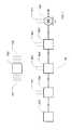
- FIG. 1is a schematic diagram of the system for detecting particles in a gas by vapor condensation on particles to form droplets and detecting the droplets so formed by an optical light-scattering detector.
- FIG. 2is a longitudinal sectional view of saturator 300 of FIG. 1 .
- FIG. 3is a sectional view of saturator 300 of FIG. 1 in a transverse direction to the direction of gas flow.
- FIG. 4is a vertical sectional view of condenser 400 of FIG. 1 .
- FIG. 5is a sectional view of in another embodiment of a condenser.
- FIG. 6is a sectional view of condenser 400 showing circulatory gas flow created by a gas jet impinging on the wall of a cylindrically shaped chamber in a perpendicular direction.
- FIG. 7is the same sectional view of condenser 400 as shown in FIG. 6 but illustrating a gas jet with small linear momentum creating a circulatory gas flow along the cold condensing wall ending with the flow becoming mixed prior to reaching the end of the full flow path along the cold condenser wall.
- FIG. 8is the same sectional view of condenser 400 as shown in FIG. 6 with a tangential gas flow inlet to create a circulatory gas flow in the chamber causing the gas to cool and mix leading to vapor super-saturation, condensation and droplet growth
- FIG. 9is a vertical sectional view of a conical condenser.
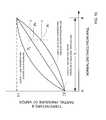
- FIG. 10is a graphical view illustrating the basis of the theoretical analysis leading to the results shown in FIG. 11 .
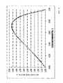
- FIG. 11is a graphical view illustrating the theoretical saturation ratio, S created in the circulatory gas flow condenser of the present disclosure showing the dependence of S on the cooling parameter, f.
- FIG. 12is a graphical view illustrating the theoretical relationship between the saturation ratio, S, and the minimum diameter, d, of particles on which vapor will condense to form droplets for detection according to the Kelvin equation, with the diameter, d, being commonly referred to as the Kelvin equivalent diameter.
- FIG. 13is a sectional view of another embodiment of a condenser
- FIG. 1illustrates a condensation particle detecting apparatus generally indicated at 90 according to the present disclosure.
- the apparatus 90includes a pump, 100 , to maintain a steady gas flow through the system and allow gas carrying suspended particles from source 200 to flow through, the pump speed being adjustable in order to adjust or control the rate of gas flow to a desired value.
- Source 200can be the ambient atmosphere, the atmosphere of a clean-room, or simply a source of gas-borne particles being sampled into the system for detection.
- the apparatus 90also includes a saturator, 300 , to saturate the gas with vapor and a condenser, 400 , to create a super-saturated vapor atmosphere in which vapor can condense on particles to form droplets for detection by the downstream detector, 600 .
- the apparatus 90includes an electronic controller, 700 , with the needed circuitry to receive output signal from various sensors in the system 90 and provide the needed control to operate the individual system components in a consistent and repeatable manner.
- Typical parameters that need to be monitored and controlledinclude temperature, flow rate, liquid level, and those pertaining to droplet detection by light scattering, such as the output power of the laser light source, sensitivity of the photo-diode or photomultiplier detector, gain and threshold settings for the detecting circuitry, among others.
- All system componentssuch as pump 100 , saturator 300 , condenser 400 , and detector 600 are provided with the requisite input and output lines 101 , 301 , 401 , and 601 to communicate with controller 700 and maintain the individual system components to the desired operating point in the sensed and controlled parameters, controller 700 being provided with its own input and output lines 701 and 702 for communication and control purposes.
- the apparatus of this disclosureis designed so that gas-borne particles will form the nucleus of condensation in a super-saturated vapor atmosphere to condense vapor on particles and form droplets for detection.
- the particles forming the nucleus of condensationare too small to be detected directly by light scattering detector 600 .
- the particlesare detected indirectly as a result of vapor having condensed on the particles to form droplets of a considerably larger size, thereby making the small non-detectable particles detectable by light scattering.
- In the ambient atmospherefor instance, there are numerous particles smaller than about 100 nm in diameter. Such particles are generally very difficult to detect by an optical, light scattering approach.
- the apparatus 90is therefore also known by the name “condensation nucleus counter,” or CNC.
- the saturator and condenser in a condensation particle countercan thus be viewed as a particle size magnifier helping to make a small, non-detectable particle into a large detectable droplet by vapor condensation and droplet growth.
- the CPCis a unique instrument and an important device for aerosol measurement.
- aerosolrefers to a gas containing suspended particles.
- the most common gasis air.
- gasessuch as nitrogen, helium, hydrogen, oxygen, etc. can also be the gaseous medium in which the particles are suspended.
- the CPCtherefore, is useful not only for airborne particle measurement, but for the measurement of gas-borne particles in general.
- FIG. 2is a longitudinal sectional view of saturator 300 along the direction of gas flow as indicated by arrows 302 .
- a sectional view in the transverse direction perpendicular to the direction of gas flowis shown in FIG. 3 .
- Saturator 300is provided with an enclosure 305 with attached electric heater 320 and temperature sensor 330 in order to control the enclosure temperature to a desired set-point value.
- Enclosure 305forms an envelope around chamber 310 in which a liquid is placed to generate vapor for saturating a gas flowing through the chamber.
- FIG. 3shows a liquid working fluid 340 which is filled to level 345 in the chamber.
- porous plates 350In addition to the working fluid 340 , which provides the source of vapor, a multitude of porous plates 350 , preferably porous metal plates, is placed in the chamber and partially immersed in the liquid.
- the porous platesare positioned substantially parallel to the flow of gas through the chamber.
- the interstitial pore space of the porous panelsis filled with working fluid 340 including the portion of the porous panel in the gas-filled space above liquid surface 345 .
- the porous panelsare filled with liquid working fluid 340 thereby making the porous panels fully wetted by liquid. Since all parts of the system are in close thermal contact with one another, the entire assembly, including the enclosure 310 , porous metal panels 350 , and working fluid 340 contained therein are heated to substantially the same uniform temperature.
- Enclosure 305is provided with an inlet, 360 , for the gas carrying suspended particles to enter and an outlet, 365 , for the gas to exit.
- the gasAs gas carrying suspended particles flows through the gas flow passageways between the liquid-filled, wet porous panels 350 , the gas is heated by the hot, wet porous panels 350 .
- liquid evaporating from the wet panel surfacewill generate vapor to saturate the gas (with suspended particles) with vapor.
- the gasupon exiting the saturator thus becomes heated and is substantially saturated with vapor.
- the saturatoris designed so that the gas will attain a selected temperature T 1 and is substantially saturated with vapor at that temperature upon its exit from the saturator.
- Saturator 300can also be designed with a pre-heater to pre-heat the gas to substantially the same temperature as the saturator. The gas so preheated can then be saturated with vapor as it flows along the liquid-filled, wet porous panels in the saturator. Either of the above approaches can be used to heat the gas and saturate the gas with vapor.
- saturator 300 in FIG. 2 and FIG. 3shows heater 320 to be attached to the top of enclosure 310 to insure that the top of the enclosure is slightly warmer than the remaining parts of the saturator. Vapor evaporating from the liquid surface 345 and from the surface of the porous panels, 350 , in the enclosure will thus encounter a slightly warmer inside surface 315 at the top and not condense there. Vapor condensing on the inside top surface 315 would form accumulated liquid which would fall back to liquid 340 below to cause splashing, which would generate small droplets that can be carried by the gas flow into the condenser to create a false particle count. For particle detection in a clean-room with low airborne particle concentration, a false count will contribute to the measurement error and must be avoided.
- a multitude of porous panels 350is provided in saturator 300 in order to provide a multitude of wet panel surfaces to generate vapor.
- a very large wetted surface areacan be created in a small physical volume, thus allowing a high volume of gas to flow through and be saturated with vapor.
- a single porous panelis sufficient.
- a single panel immersed in liquidwill provide two wetted surfaces above the liquid from which the liquid can evaporate to generate vapor, which then diffuses into the gas stream flowing nearby.
- a multitude of platesare used to provide enough surface area for vaporization.
- ten plates spaced 3 mm apart from each otherhave proven sufficient to achieve the desired vapor saturation results needed for the application.
- the parallel panelswill thus make it possible to design a CPC 90 with a high volumetric flow rate of gas in order to detect particles having a low airborne concentration such as that in a clean-room.
- Traditional CPCsare designed with the liquid evaporating from a wet-wall saturator with the gas flow passageway being surrounded by a porous material wall filled with the working fluid.
- the flow passagewaycan have a rectangular cross-section, as shown in U.S. Pat. No. 4,790,650, or a tubular flow passageway with a circular cross-section as shown in U.S. Pat. No. 6,829,044B2.
- liquidcan only evaporate from the wet rectangular or circular walls surrounding the gas-flow passageway with no additional surfaces being provided to generate vapor for saturating the gas.
- additional evaporative surface areasare provided within the overall envelope of the gas-flow passageway walls to generate vapor for saturating the gas.
- This approachgreatly increases the surface area that can be placed in the gas flow passageways to saturate a high rate of gas flow through the passageways.
- the design of this disclosureis also very flexible making it possible to increase the wet evaporative surface to as large an area as necessary in order to saturate the gas at any desired rate of gas flow.
- the lack of a suitable saturator with an adequate evaporative capacityhas limited the maximum gas flow rate that can be achieved in the traditional CPC design in the past. Such flexibility is now provided in the saturating apparatus design of the present disclosure.
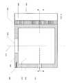
- FIG. 4shows the vertical sectional view of condenser 400 in one embodiment.
- the condenseris made from a rectangular shaped metal piece containing a cylindrically shaped chamber 410 with the chamber's axis 415 placed in a vertical orientation.
- Chamber 410has an inlet 420 for a gas to enter and an outlet 425 for the gas to exit.
- Inlet 420is located on the vertical side wall of the cylinder, while outlet 425 is located on a top wall.
- a thermoelectric cooling (TEC) module 430is placed in close thermal contact with metal piece 405 to cool the metal piece to a desired operating temperature, T 2 .
- TECthermoelectric cooling
- Coolingis achieved by applying a DC voltage to cause a DC current of a specified polarity to flow through TEC module 430 to create the desired thermoelectric cooling effect.
- Heat generated by the thermoelectric cooling moduleis dissipated to the ambient by an extended surface heat exchanger, 435 , by natural or forced convection.
- the metal piece and the metal wall 440 of chamber 410are also cooled to substantially the same temperature T 2 .
- a temperature sensor, 445in contact with metal piece 405 senses the temperature of the metal piece.
- the electric power input to TEC module 430can be varied to allow temperature T 2 to be controlled to a desired set-point value.
- the condenser 400may need to be heated to a temperature above the surrounding environment in which the condenser is placed.
- the current flowcan be reversed by applying a voltage having a polarity opposite to that needed for cooling.
- TEC module 430therefore, can be placed in the heating mode working as a heat pump to pump heat from the surrounding environment to heat the condenser.
- a separate electric heatercan be used to provide heating to the condenser, and keeping it at a temperature above the surrounding environment.
- the relatively warmer gasencounters the relatively cooler condenser chamber wall 440 , thereby causing the relatively warmer gas to cool forming a gas stream having a non-uniform temperature distribution.
- the temperature distribution in the gasbecomes non-uniform because the gas stream moving closest to the cold condenser wall 400 will lose more heat than gas streams that are farther away from the wall.
- vapor in the gaswill diffuse to the chamber wall 440 to condense on the wall.
- the vapor concentration in the gaswill also become non-uniform since the gas stream moving closest to the wall would lose more vapor by condensation on the wall than streams that are farther away.
- the vapor concentration in the gaswill also become non-uniform.
- This non-uniformly cooled gas stream having a non-uniform temperature and a non-uniform vapor concentration profilethen mixes when the gas flow becomes turbulent thereby creating a mixture having a more uniform temperature and vapor concentration.
- the resultis the formation of a super-saturated vapor atmosphere in which vapor can condense on particles to form droplets.
- the mixturethen flows out of chamber 410 through outlet 425 to droplet detector 600 located downstream of condenser 400 as shown in FIG. 1 .
- FIG. 5An embodiment with additional features of the condenser 400 is shown in FIG. 5 .
- the length of cylindrical chamber 410is extended by providing a second condensing chamber 426 downstream of condensing chamber 410 .
- Outlet 425 for chamber 410then becomes the inlet for chamber 426 .
- Outlet 425is smaller in cross-sectional area than chambers 410 and 426 , thus forming a restrictive flow passageway for the gaseous mixture from chamber 410 to flow through and enter chamber 426 .
- the gas flow in this restrictive flow passagewayis sufficient to create a turbulent gas jet downstream of the restriction.
- the fluid turbulence in the gas jetcreates additional mixing to make the gas mixture in chamber 426 more homogeneously mixed than the mixture in chamber 420 .
- chamber 426provides additional volume for the gas to reside and flow through, thereby increasing the overall residence time of the mixture in chambers 410 and 426 to give the droplets more time to grow to a larger size prior their exit through outlet 428 with the gas flow to the downstream droplet detector 600 .
- FIG. 6is a horizontal sectional view of FIG. 4 showing the cylindrically shaped chamber 410 along section A-A of FIGS. 4 and 5 .
- Thermoelectric module 430 and heat sink 435are similarly labeled in both FIGS. 4 and 5 and FIG. 6 .
- the gas with suspended particlesforms a gas jet travelling along path 425 through the intervening cylindrical chamber space to impinge on the opposite wall of the chamber.
- the gas jetUpon hitting wall 440 the gas jet is deflected side ways to create a circulatory gas flow along paths 445 and 450 . As the gas flows along these paths, it loses heat to the adjacent cold condenser wall 440 by convection.
- the vaporwill also condense on the surface of the cold condenser wall.
- the condensed liquidwill drain by gravity along the condenser wall to a liquid reservoir below, which is not shown.
- the condenser 400is maintained at a relatively cooler temperature, T 2 , compared to the temperature T 1 of saturator 300 .
- T 2the temperature of the circulatory gas flow pathways, or streamlines, 445 and 450 .
- the gashaving cooled by contact with wall 440 , and having lost some vapor by condensation, will have a non-uniform temperature distribution across the streamlines.
- flow paths and streamlinesare synonymous terms in laminar flow, the fluid does not inter-mix.
- the fluidtravels in a well defined path to form a well defined streamline.
- turbulent flowthere is turbulent mixing of the fluid.
- the flow paths, or streamlinesrefer to the pathway or streamline of the mean flow.
- superimposed on the mean flow pathway or streamlineare turbulent eddies that cause the flow to move rapidly in the lateral direction.
- the partial pressure of vapor in the gas streamwill also become non-uniformly distributed across the streamlines due to the varying amount of vapor that has diffused across the streamlines to condense on the wall of the cold-wall condenser.
- the remaining kinetic energy of the flowing gas streamwill cause the gas stream to breakup into turbulent eddies, filling the space in the core of the circulatory gas flow with a turbulent mixture.
- the turbulent gas flowis in the turbulent core.
- the turbulent gas flowhelps make the mixture become more uniformly mixed with a substantially uniform temperature and partial vapor pressure in the gas.
- the flow in this circulatory gas flow condenseris therefore in the form of a vortex flow with a relatively higher velocity gas flow circulating around a turbulent vortex core to produce the mixing needed for the vapor to become super-saturated and condense on particles to form droplets.
- the gas flow pattern depicted in FIG. 6is that from a gas flowing at a relatively high volumetric rate of flow through an inlet 420 with a relatively small cross-sectional area, thereby creating a high velocity gas jet with a high linear momentum in the direction of the gas jet.
- This high momentum gas jetupon traveling to the end of the circulatory flow paths 445 and 450 adjacent to the condenser wall would have lost some linear momentum due to fluid friction, but would still retain sufficient momentum for the gas to flow in the forward direction, causing it to spiral inward as shown by arrows, 452 , 454 , and 456 , toward the center 460 of a vortex as depicted in the top half of FIG. 6 .
- the vortex flow depicted in the top half of FIG. 6has a counter clockwise rotation.
- the vortex formed in the bottom half the FIG. 6is similar to that in the upper half except the direction of rotation of the vortex is clockwise.
- a gas entering the chamber at a relatively low volumetric rate of gas flow through an inlet with a relatively larger cross sectional areawill carry less momentum.
- Such a gaswould form a jet travelling through the cylindrical chamber as in FIG. 7 at a relatively low speed.
- the gas jetupon hitting wall 440 would be deflected sideways to flow along paths 445 and 450 adjacent to the cold chamber wall 440 .
- the momentum of the flowing gas streamis too low for it to flow beyond the end of the path at 412 and 414 .
- the gashaving lost much of its forward momentum will flow to the vortex core region with much less turbulent mixing compared to that depicted in FIG. 6 . Mixing will still occur, but with a lesser intensity than that depicted in FIG. 6 .
- the top of the chamberis provided with outlet 425 with a smaller cross-sectional area than that of the cylindrical chamber to confine the circulating gas flow in chamber 410 and cause it to mix prior to its exit from the chamber, thus helping the gas flowing out of the chamber to be uniformly mixed.
- a second chambercan also be provided as shown in FIG. 5 to provide additional volume for the mixture to undergo additional mixing and provide more residence time for the droplets to grow in the chamber.
- the jet of gas issuing out of orifices 420 and 425will be turbulent if the Reynolds number of the flow is larger than about 100.
- the cross-sectional shape of the cylindrical chamberis generally circular, but other shapes, such as that of an ellipse, a square, a rectangle, and other polygonal shapes with straight interior surface walls, or a combination of shapes formed by straight and curved wall can also be used.
- the three-dimensional chamberalso does not need to be cylindrical in shape as depicted in FIG. 4 .
- Other chamber shapessuch as the shape of a sphere, an ellipsoid, a pyramid, a cube, a rectangle with length, width and height that are not equal, and other polyhedral shapes formed by flat walls, or walls with some that are flat and some that are curved.
- the circulatory gas flow patterncan develop in a wide range of chamber shapes, the precise shape of the chamber is relatively unimportant, The required circulatory gas flow pattern can develop in many different chamber shapes and still suffice to provide the needed cooling and mixing to generate a super-saturated vapor in the chamber for condensation and droplet growth on particles.
- the modern continuous flow CPCsare organic fluid based in which an organic working fluid such as alcohol is used to generate vapor for condensation, with butyl alcohol being the most widely used working fluid.
- An approach to adiabatic gas expansion for gas cooling in a continuous flow CPCis described in U.S. Pat. No. 6,980,284 in which a vapor saturated gas is expanded through a small diameter capillary tube under condition of high pressure drop to create sonic flow and adiabatic gas cooling in the capillary tube.
- the laminar flow, cold wall condenseris therefore normally used with an organic working fluid, such as butyl alcohol, because the relatively lower molecular diffusivity of the higher molecular weight organic working fluid would prevent rapid vapor depletion thereby making it possible for vapor super-saturation to develop in the laminar flow stream for condensation and droplet growth.
- an organic working fluidsuch as butyl alcohol
- U.S. Pat. No. 6,712,881then describes a laminar flow CPC of a non-traditional design for use with water as a working fluid.
- a hot, wet-wall condenseris used in a laminar flow condenser to generate vapor for diffusion into a cold laminar gas stream flowing through the condenser.
- Water vaporis added to the flowing cold gas during its passage through the hot wet-wall condenser to create super-saturation for vapor condensation and droplet growth.
- the apparatushas since become a commercially available device.
- Another approach to using water as a working fluidis the continuous flow device described in U.S. Pat. No. 5,803,338 in which two water-vapor saturated gas streams—one hot and one cold—are mixed to create a mixture stream having a super-saturated vapor to condense on particles and form droplets.
- the CPC of the present disclosureis similar to the traditional alcohol based continuous flow CPC in one respect in that hot vapor-laden gas containing suspended particles is introduced into a cold wall condenser to create vapor super-saturation for condensation and droplet growth.
- the condenser of the present disclosureuses a circulatory gas flow to cool the gas and create vapor super-saturation for condensation and droplet growth in a chamber under turbulent flow conditions, while the gas flow in the traditional continuous flow condenser is both laminar and uni-directional, thus non-circulatory.
- the circulatory gas flow condenser of the present disclosureworks well both with water as a working fluid, as well as an organic working fluid, such as alcohol.
- the apparatus of the present disclosureuses only one gas stream in a single condenser chamber to create a non-uniform gas stream in terms of temperature and vapor partial pressure, which is then mixed thoroughly by fluid turbulence to create vapor super-saturation for condensation particle counting.
- the condensing apparatus of the present disclosureis therefore simpler, and easier to implement than the two-stream apparatus of U.S. Pat. No. 5,803,338.
- Other mixing type CPCssuch as those described in U.S. Pat. No. 4,449,816 and No. 6,567,157 also use a hot and a cold gas stream and mix the two to create the needed super-saturation for condensation and droplet growth.
- FIG. 8shows an embodiment with circulatory gas flow by having the gas inlet 460 oriented to form a gas stream flowing along the periphery, i.e. the tangent of the circular section of the vertical cylindrical chamber. This tangential gas flow then moves along path 465 to cool the gas, causing it to mix with the incoming hot, vapor laden gas entering the chamber through inlet 460 to create a mixture having a super-saturated vapor atmosphere to condense vapor on particles and form droplets.
- the vortex flow that may develop in such a tangential inlet flow deviceis depicted by arrows, 470 , 472 , 474 , and 476 in FIG. 8 .
- the vortex flowwill develop only when the volumetric gas flow rate through the apparatus is sufficiently high and the cross-sectional area of the gas inlet is sufficiently small for a gas stream with a sufficiently high momentum to develop and create the vortex flow pattern in the condenser.
- the full vortex flowmay not form, but the relatively slow moving gas flow will still have sufficient momentum to create fluid turbulence for mixing and creating vapor super-saturation.
- the cylindrical chamber in both the one embodiment of FIG. 4 with a normal flow inlet and the other embodiment of FIG. 8can have any cross-sectional shape, including circular, elliptical, square, rectangular, polygonal, among others.
- the preferred cross-sectional shapeis circular.
- FIG. 9yet illustrates another example of a circulatory gas flow by locating gas inlet 420 on the side wall of a vertically oriented, conical chamber 450 .
- the conical shaped chambercan be used advantageously to improve the performance of the circulatory gas flow condenser and provide a more smooth aerodynamic flow transition from the larger conical base to the smaller flow outlet 425 on the top.
- Other orientations of the conically shaped chambercan also be used to achieve specific design advantages. Such advantages will become obvious to those skilled in the art of designing condensation particle counters after having studied the present disclosure. Therefore they will not be further described.
- FIG. 10shows graphically the temperature distribution across the streamlines near the end of the flow path 450 in FIG. 6 along the direction of line 448 , which is perpendicular to the cylindrical wall surface at that point.
- the gas temperature at point Awould be the same as the temperature of the wall, T 2 .
- the temperature at point Bis not greatly different or is substantially the same as the temperature of the gas, T 1 , entering the chamber through inlet 420 . This is depicted by curve 1 in FIG. 10 .
- the line connecting the ends of Curve 1is a straight line, Line 2 , on which one can depict the bulk temperature, T b , of the gas, following the turbulent mixing of the non-uniformly cooled gas stream in the turbulent vortex core, a region of space occupied by the sequences of arrow 452 , 454 , and 456 , and the center, 460 of the vortex core in FIG. 6 .
- the bulk temperature of a gas with a non-uniform temperature distributionis the temperature of the gas following thorough mixing of the gas under adiabatic conditions. Mixing is adiabatic if no heat is added or removed from the gas during the mixing process.
- Point C on Line 2shows the bulk temperature, T b , of the gas under one specific set of operating conditions of the apparatus.
- the stream line moving close to the cold wall surfacewill quickly cool to the temperature of the wall, T 2 .
- Vaporwill also condense from the gas stream, so that the vapor pressure of the gas will be the saturation vapor pressure of water at T 2 .
- Gas flowing along streams at varying distances from the cold condenser wallwill lose varying amounts of vapor by vapor diffusion as the individual streams reach the end of the path 450 .
- the vapor pressure of water in the overall gas streamwill thus also be non-uniform.
- the main streamwill be thoroughly mixed, creating a uniformly mixed stream having a bulk partial pressure of water, p b .
- the bulk vapor partial pressurebeing the partial pressure of vapor in the bulk gas after thorough mixing without gaining or losing vapor during the process.
- the rate of heat loss by a gas flowing adjacent to a cold wallis dependent on the thermal diffusivity of the gas and the nature of the gas flow.
- the rate of vapor lossdepends on the molecular diffusion of the vapor in the gas and the nature of gas flow.
- the major resistance to heat and vapor loss to the cold condenseroccurs in the laminar boundary sub-layer near the wall.
- the rate of heat loss and vapor lossare proportional to the thermal diffusivity of the gas and the molecular diffusivity of vapor in the gas.
- the vapor diffusivityis not greatly different from the thermal diffusivity of the air. For simplicity, they are assumed to be equal.
- Curve 3 of FIG. 10depicts the saturation vapor pressure of water at the bulk temperature, T b , of the gas. Since vapor pressure increases more rapidly with increasing temperature, Curve 3 is a concave curve facing upward as depicted. This shows that the bulk vapor pressure, p b , in the gas following mixing is higher than the saturation pressure, P s , at the bulk temperature of the gas/vapor mixture.
- the ratio of p b and p sis the saturation ratio
- FIG. 11shows the result of a theoretical analysis based on the above approach.
- the theoretically calculated saturation ratio, Sis plotted against the cooling parameter
- T 1is the temperature of the saturated gas entering the condenser
- T 2is the temperature of the condenser wall
- T bis the bulk temperature of the cooled gas produced by the circulatory gas flow along the cold wall condenser.
- FIG. 11shows that super-saturation can develop only when there is partial cooling of the gas to an intermediate temperature, so that T 2 ⁇ T b ⁇ T 1 , or 0 ⁇ f ⁇ 1.0, and that the maximum super-saturation is developed when f ⁇ 0.7 for the specific example shown.
- the condenser chambershould be designed to achieve approximately 70% of the maximum cooling possible.
- FIG. 13shows yet another approach to creating vapor super-saturation for condensation on particles to form droplets for detection and/or counting.
- FIG. 13is similar to FIG. 5 except gas cooling is accomplished by a laminar gas stream flowing in a cold tube.
- warm gas containing vapor and particlesis introduced into a cooler tubular shaped chamber 410 with a generally circular cross-section.
- the gasflows upward in the chamber as indicated by arrows 485 .
- This flowing gasthen loses heat by thermal diffusion to the cold chamber wall.
- vaporis lost to the wall by molecular diffusion and condensation on the wall.
- Streamlines that are close to wall 440will lose heat and vapor more quickly than those that are farther away.
- the temperature of the gas and the partial pressure of vapor in the gaswill become non-uniform as the gas flows upward in the chamber
- this non-uniformly cooled gas with a non-uniformly distributed vapor partial pressure in the gasthen flows out of chamber 410 through flow restriction 425 to form a turbulent gas jet in chamber 426 .
- the turbulencecauses the gas to mix, thus making both the gas temperature and the vapor partial pressure in the gas more uniform, resulting in the creation of a super-saturated vapor which condenses on particles and forms droplets.
- the processis similar to that in the circulatory gas condenser of FIG. 4 except in the preferred embodiment of FIG. 4 , cooling and mixing of the gas takes place in a single chamber, whereas in the embodiment of FIG. 13 two separate chambers are used, one for gas cooling and the other for mixing.
- the embodiment of FIG. 13is equivalent to that of adding a mixing chamber downstream of a conventional laminar flow cold-wall condenser. While the traditional laminar cold wall condenser by itself cannot create vapor super-saturation to form droplets when water is used as the working fluid as discussed in U.S. Pat. No. 6,712,881, the embodiment of FIG. 13 has made it it possible to create a super-saturated vapor to condense on particles and form droplets for counting when water is used as the working fluid.
Landscapes
- Chemical & Material Sciences (AREA)
- Dispersion Chemistry (AREA)
- Physics & Mathematics (AREA)
- Health & Medical Sciences (AREA)
- Life Sciences & Earth Sciences (AREA)
- Analytical Chemistry (AREA)
- Biochemistry (AREA)
- General Health & Medical Sciences (AREA)
- General Physics & Mathematics (AREA)
- Immunology (AREA)
- Pathology (AREA)
- Sampling And Sample Adjustment (AREA)
- Investigating Or Analysing Materials By Optical Means (AREA)
Abstract
Description
The present application is a divisional application of U.S. patent application Ser. No. 12/872,697, filed Aug. 31, 2010 which is based on and claims the benefit of U.S. provisional patent application Ser. No. 61/252,243, filed Oct. 16, 2009, the contents of which are hereby incorporated by reference in their entirety.
The present disclosure describes a method and an apparatus for detecting particles in a gas by condensing vapor on the particles to form droplets, which are then detected by an optical, light-scattering detector. Instruments using vapor condensation on particles to form droplets for detection are referred to as condensation particle counters (CPC), or as condensation nucleus counters (CNC). A variety of working fluids can be used to generate vapor for condensation. The most common working fluids are butyl alcohol and water.
Condensation particle counters are useful in many applications. In air pollution and climate research, for instance, the instrument is often used with an electrical mobility analyzer to determine the concentration and size distribution of particles in the ambient atmosphere. The instrument can also be used to detect particulate contaminants suspended in clean-room air for clean-room monitoring and contamination control purposes. In addition, CPC is widely used in laboratory research to study the property and behavior of small airborne particles.
The most important process in a CPC is the process of vapor generation, condensation and droplet growth. The present disclosure describes a new approach to creating super-saturation for vapor condensation and droplet growth, leading to a compact measuring device with improved performance characteristics.
The present disclosure describes a method and apparatus for detecting particles in a gas by saturating the gas with vapor at one temperature and causing the gas to flow through a chamber with walls at a different temperature, thereby changing the gas temperature in the chamber. At the same time the gas flow is made turbulent causing the gas to mix in the chamber to create super-saturation for vapor to condense on said particles and form droplets, which are then detected and counted by an optical light-scattering detector.
In addition, theapparatus 90 includes an electronic controller,700, with the needed circuitry to receive output signal from various sensors in thesystem 90 and provide the needed control to operate the individual system components in a consistent and repeatable manner. Typical parameters that need to be monitored and controlled include temperature, flow rate, liquid level, and those pertaining to droplet detection by light scattering, such as the output power of the laser light source, sensitivity of the photo-diode or photomultiplier detector, gain and threshold settings for the detecting circuitry, among others. All system components such aspump 100,saturator 300,condenser 400, anddetector 600 are provided with the requisite input andoutput lines controller 700 and maintain the individual system components to the desired operating point in the sensed and controlled parameters,controller 700 being provided with its own input andoutput lines
The apparatus of this disclosure is designed so that gas-borne particles will form the nucleus of condensation in a super-saturated vapor atmosphere to condense vapor on particles and form droplets for detection. The particles forming the nucleus of condensation are too small to be detected directly bylight scattering detector 600. The particles are detected indirectly as a result of vapor having condensed on the particles to form droplets of a considerably larger size, thereby making the small non-detectable particles detectable by light scattering. In the ambient atmosphere, for instance, there are numerous particles smaller than about 100 nm in diameter. Such particles are generally very difficult to detect by an optical, light scattering approach. By growing the particles to a larger droplet size by vapor condensation and droplet growth and detecting the grown droplets by light scattering, the existence of the small condensation nuclei in the gas can be confirmed. Theapparatus 90 is therefore also known by the name “condensation nucleus counter,” or CNC. The saturator and condenser in a condensation particle counter can thus be viewed as a particle size magnifier helping to make a small, non-detectable particle into a large detectable droplet by vapor condensation and droplet growth.
The CPC is a unique instrument and an important device for aerosol measurement. In scientific usage, aerosol refers to a gas containing suspended particles. The most common gas is air. Other gases, such as nitrogen, helium, hydrogen, oxygen, etc. can also be the gaseous medium in which the particles are suspended. The CPC, therefore, is useful not only for airborne particle measurement, but for the measurement of gas-borne particles in general.
The design ofsaturator 300 inFIG. 2 andFIG. 3 showsheater 320 to be attached to the top ofenclosure 310 to insure that the top of the enclosure is slightly warmer than the remaining parts of the saturator. Vapor evaporating from theliquid surface 345 and from the surface of the porous panels,350, in the enclosure will thus encounter a slightly warmer insidesurface 315 at the top and not condense there. Vapor condensing on the insidetop surface 315 would form accumulated liquid which would fall back toliquid 340 below to cause splashing, which would generate small droplets that can be carried by the gas flow into the condenser to create a false particle count. For particle detection in a clean-room with low airborne particle concentration, a false count will contribute to the measurement error and must be avoided.
A multitude ofporous panels 350 is provided insaturator 300 in order to provide a multitude of wet panel surfaces to generate vapor. By using a large number of closely spaced panels substantially parallel to the flow of gas as shown inFIG. 3 , a very large wetted surface area can be created in a small physical volume, thus allowing a high volume of gas to flow through and be saturated with vapor. At low volumetric rate of gas flow, a single porous panel is sufficient. A single panel immersed in liquid will provide two wetted surfaces above the liquid from which the liquid can evaporate to generate vapor, which then diffuses into the gas stream flowing nearby. At higher gas flows, a multitude of plates are used to provide enough surface area for vaporization. In one implementation of the saturator, ten plates spaced 3 mm apart from each other have proven sufficient to achieve the desired vapor saturation results needed for the application. The parallel panels will thus make it possible to design aCPC 90 with a high volumetric flow rate of gas in order to detect particles having a low airborne concentration such as that in a clean-room.
Traditional CPCs are designed with the liquid evaporating from a wet-wall saturator with the gas flow passageway being surrounded by a porous material wall filled with the working fluid. The flow passageway can have a rectangular cross-section, as shown in U.S. Pat. No. 4,790,650, or a tubular flow passageway with a circular cross-section as shown in U.S. Pat. No. 6,829,044B2. In these traditional saturator designs, liquid can only evaporate from the wet rectangular or circular walls surrounding the gas-flow passageway with no additional surfaces being provided to generate vapor for saturating the gas.
In the vertical parallel panel design of the present disclosure additional evaporative surface areas are provided within the overall envelope of the gas-flow passageway walls to generate vapor for saturating the gas. This approach greatly increases the surface area that can be placed in the gas flow passageways to saturate a high rate of gas flow through the passageways. The design of this disclosure is also very flexible making it possible to increase the wet evaporative surface to as large an area as necessary in order to saturate the gas at any desired rate of gas flow. The lack of a suitable saturator with an adequate evaporative capacity has limited the maximum gas flow rate that can be achieved in the traditional CPC design in the past. Such flexibility is now provided in the saturating apparatus design of the present disclosure.
In some cases, thecondenser 400 may need to be heated to a temperature above the surrounding environment in which the condenser is placed. In which case, the current flow can be reversed by applying a voltage having a polarity opposite to that needed for cooling.TEC module 430, therefore, can be placed in the heating mode working as a heat pump to pump heat from the surrounding environment to heat the condenser. Alternatively, a separate electric heater can be used to provide heating to the condenser, and keeping it at a temperature above the surrounding environment.
As the gas containing vapor and suspended particles flows throughinlet 420 into the thermoelectrically cooled condensingchamber 410, the relatively warmer gas encounters the relatively coolercondenser chamber wall 440, thereby causing the relatively warmer gas to cool forming a gas stream having a non-uniform temperature distribution. The temperature distribution in the gas becomes non-uniform because the gas stream moving closest to thecold condenser wall 400 will lose more heat than gas streams that are farther away from the wall. At the same time, vapor in the gas will diffuse to thechamber wall 440 to condense on the wall. The vapor concentration in the gas will also become non-uniform since the gas stream moving closest to the wall would lose more vapor by condensation on the wall than streams that are farther away. As a result, the vapor concentration in the gas will also become non-uniform. This non-uniformly cooled gas stream having a non-uniform temperature and a non-uniform vapor concentration profile then mixes when the gas flow becomes turbulent thereby creating a mixture having a more uniform temperature and vapor concentration. The result is the formation of a super-saturated vapor atmosphere in which vapor can condense on particles to form droplets. The mixture then flows out ofchamber 410 throughoutlet 425 todroplet detector 600 located downstream ofcondenser 400 as shown inFIG. 1 .
The approach to creating vapor saturation by cooling and mixing a gas in a cold-wall chamber in the manner described above is previously unknown. The theoretical basis of such an approach will be explained more fully later in this disclosure.
An embodiment with additional features of thecondenser 400 is shown inFIG. 5 . The length ofcylindrical chamber 410 is extended by providing asecond condensing chamber 426 downstream of condensingchamber 410.Outlet 425 forchamber 410 then becomes the inlet forchamber 426.Outlet 425 is smaller in cross-sectional area thanchambers chamber 410 to flow through and enterchamber 426. The gas flow in this restrictive flow passageway is sufficient to create a turbulent gas jet downstream of the restriction. The fluid turbulence in the gas jet creates additional mixing to make the gas mixture inchamber 426 more homogeneously mixed than the mixture inchamber 420. In addition,chamber 426 provides additional volume for the gas to reside and flow through, thereby increasing the overall residence time of the mixture inchambers outlet 428 with the gas flow to thedownstream droplet detector 600.
The gas flow pattern depicted inFIG. 6 is that from a gas flowing at a relatively high volumetric rate of flow through aninlet 420 with a relatively small cross-sectional area, thereby creating a high velocity gas jet with a high linear momentum in the direction of the gas jet. This high momentum gas jet upon traveling to the end of thecirculatory flow paths center 460 of a vortex as depicted in the top half ofFIG. 6 . As the gas flow spirals inward toward thecenter 460, it will continue to shed turbulent eddies to dissipate the kinetic energy carried by the flow, thereby creating a turbulent region in the vortex core. The vortex flow depicted in the top half ofFIG. 6 has a counter clockwise rotation. The vortex formed in the bottom half theFIG. 6 is similar to that in the upper half except the direction of rotation of the vortex is clockwise.
In contrast to the above, a gas entering the chamber at a relatively low volumetric rate of gas flow through an inlet with a relatively larger cross sectional area will carry less momentum. Such a gas would form a jet travelling through the cylindrical chamber as inFIG. 7 at a relatively low speed. The gas jet, upon hittingwall 440 would be deflected sideways to flow alongpaths cold chamber wall 440. The momentum of the flowing gas stream is too low for it to flow beyond the end of the path at412 and414. Upon reaching the end offlow paths FIG. 6 . Mixing will still occur, but with a lesser intensity than that depicted inFIG. 6 .
To prevent the gas flow inchamber 410 in the circulatory gas flow condenser ofFIG. 4 from flowing out ofchamber 410 prior to sufficient mixing has taken place, the top of the chamber is provided withoutlet 425 with a smaller cross-sectional area than that of the cylindrical chamber to confine the circulating gas flow inchamber 410 and cause it to mix prior to its exit from the chamber, thus helping the gas flowing out of the chamber to be uniformly mixed. As discussed earlier, a second chamber can also be provided as shown inFIG. 5 to provide additional volume for the mixture to undergo additional mixing and provide more residence time for the droplets to grow in the chamber.
The jet of gas issuing out oforifices
In various embodiments of the present disclosure including those shown inFIG. 4 throughFIG. 9 andFIG. 13 , the cross-sectional shape of the cylindrical chamber is generally circular, but other shapes, such as that of an ellipse, a square, a rectangle, and other polygonal shapes with straight interior surface walls, or a combination of shapes formed by straight and curved wall can also be used. The three-dimensional chamber also does not need to be cylindrical in shape as depicted inFIG. 4 . Other chamber shapes such as the shape of a sphere, an ellipsoid, a pyramid, a cube, a rectangle with length, width and height that are not equal, and other polyhedral shapes formed by flat walls, or walls with some that are flat and some that are curved. Since the circulatory gas flow pattern can develop in a wide range of chamber shapes, the precise shape of the chamber is relatively unimportant, The required circulatory gas flow pattern can develop in many different chamber shapes and still suffice to provide the needed cooling and mixing to generate a super-saturated vapor in the chamber for condensation and droplet growth on particles.
The approach described above of using a circulatory gas flow to create a super-saturated vapor atmosphere in a cold-wall condenser for vapor condensation and droplet growth is fundamentally different from other approaches that have been used in the past for creating vapor super-saturation for condensation particle counting. Historically, particle counting by vapor condensation and droplet growth is based on adiabatic gas expansion to cool the gas and create a super-saturated vapor atmosphere for condensation and droplet growth to occur. The gas flow in such devices is intermittent. The historically important expansion type CPC, which has an intermittent gas flow, has largely been replaced by the modem continuous flow CPCs similar to that described in U.S. Pat. No. 4,790,650. In contrast to the expansion type CPC which uses water as a working fluid, the modern continuous flow CPCs are organic fluid based in which an organic working fluid such as alcohol is used to generate vapor for condensation, with butyl alcohol being the most widely used working fluid. An approach to adiabatic gas expansion for gas cooling in a continuous flow CPC is described in U.S. Pat. No. 6,980,284 in which a vapor saturated gas is expanded through a small diameter capillary tube under condition of high pressure drop to create sonic flow and adiabatic gas cooling in the capillary tube.
In recent years, there is an interest in returning to water as a working fluid because of its abundance and non-contaminating nature. Water is also considered an “environmentally friendly” substance to use in a measuring instrument such as the CPC. As pointed out in U.S. Pat. No. 6,712,881, water does not work well in the traditional continuous flow CPC, since water would diffuse too quickly to the cold condenser walls of the laminar flow condenser to cause the gas stream to be depleted with water vapor by an amount sufficient to prevent super-saturation to develop for vapor condensation and droplet growth. The laminar flow, cold wall condenser is therefore normally used with an organic working fluid, such as butyl alcohol, because the relatively lower molecular diffusivity of the higher molecular weight organic working fluid would prevent rapid vapor depletion thereby making it possible for vapor super-saturation to develop in the laminar flow stream for condensation and droplet growth.
U.S. Pat. No. 6,712,881 then describes a laminar flow CPC of a non-traditional design for use with water as a working fluid. In this non-traditional design, a hot, wet-wall condenser is used in a laminar flow condenser to generate vapor for diffusion into a cold laminar gas stream flowing through the condenser. Water vapor is added to the flowing cold gas during its passage through the hot wet-wall condenser to create super-saturation for vapor condensation and droplet growth. The apparatus has since become a commercially available device. Another approach to using water as a working fluid is the continuous flow device described in U.S. Pat. No. 5,803,338 in which two water-vapor saturated gas streams—one hot and one cold—are mixed to create a mixture stream having a super-saturated vapor to condense on particles and form droplets.
The CPC of the present disclosure is similar to the traditional alcohol based continuous flow CPC in one respect in that hot vapor-laden gas containing suspended particles is introduced into a cold wall condenser to create vapor super-saturation for condensation and droplet growth. Unlike the traditional laminar flow condenser of the traditional design, the condenser of the present disclosure uses a circulatory gas flow to cool the gas and create vapor super-saturation for condensation and droplet growth in a chamber under turbulent flow conditions, while the gas flow in the traditional continuous flow condenser is both laminar and uni-directional, thus non-circulatory. In addition, unlike the traditional laminar flow cold-wall condenser that works well only with an organic working fluid, but not with water, the circulatory gas flow condenser of the present disclosure works well both with water as a working fluid, as well as an organic working fluid, such as alcohol. Further, in contrast to the mixing CPC of U.S. Pat. No. 5,803,338, in which two water-vapor saturated gas streams—one hot and one cold—are mixed to create super-saturation for vapor condensation and droplet growth, the apparatus of the present disclosure uses only one gas stream in a single condenser chamber to create a non-uniform gas stream in terms of temperature and vapor partial pressure, which is then mixed thoroughly by fluid turbulence to create vapor super-saturation for condensation particle counting. The condensing apparatus of the present disclosure is therefore simpler, and easier to implement than the two-stream apparatus of U.S. Pat. No. 5,803,338. Other mixing type CPCs such as those described in U.S. Pat. No. 4,449,816 and No. 6,567,157 also use a hot and a cold gas stream and mix the two to create the needed super-saturation for condensation and droplet growth.
The approach to vapor condensation and droplet growth described in the present disclosure, therefore, has resulted in an apparatus that is nearly universal in the choice of working fluid for use in the apparatus. Almost any fluid including water and those with a higher molecular weight and a correspondingly lower molecular diffusivity than water can both be used. It has also simplified the mixing CPC design by using a single gas stream in a single condenser chamber to create a non-uniform temperature distribution in a single gas and cause the gas to mix to create a super-saturated vapor atmosphere in the chamber for condensation and droplet growth.
In the embodiment ofFIG. 6 , the gas flow entering the condenser chamber through the inlet creates a gas jet impinging onto the wall of a cylindrical shaped condenser chamber in a normal, i.e. perpendicular direction.FIG. 8 shows an embodiment with circulatory gas flow by having thegas inlet 460 oriented to form a gas stream flowing along the periphery, i.e. the tangent of the circular section of the vertical cylindrical chamber. This tangential gas flow then moves alongpath 465 to cool the gas, causing it to mix with the incoming hot, vapor laden gas entering the chamber throughinlet 460 to create a mixture having a super-saturated vapor atmosphere to condense vapor on particles and form droplets. The vortex flow that may develop in such a tangential inlet flow device is depicted by arrows,470,472,474, and476 inFIG. 8 . As previously noted in the normal inlet condenser ofFIG. 5 , the vortex flow will develop only when the volumetric gas flow rate through the apparatus is sufficiently high and the cross-sectional area of the gas inlet is sufficiently small for a gas stream with a sufficiently high momentum to develop and create the vortex flow pattern in the condenser. At a lower volumetric gas flow rate through an inlet with a relatively large cross-sectional area, the full vortex flow may not form, but the relatively slow moving gas flow will still have sufficient momentum to create fluid turbulence for mixing and creating vapor super-saturation. The cylindrical chamber in both the one embodiment ofFIG. 4 with a normal flow inlet and the other embodiment ofFIG. 8 can have any cross-sectional shape, including circular, elliptical, square, rectangular, polygonal, among others. The preferred cross-sectional shape is circular.
The process of using a circulatory gas flow condenser for creating vapor super-saturation, condensation and droplet growth can be analyzed theoretically to aid in the design of the actual apparatus. Although the complicated gas flow patterns in a circulatory gas flow condenser prevents an exact analysis to be made, an analysis made under certain simplifying assumptions can be helpful to improve the understanding of the operation of the circulatory gas flow condenser and the parameters affecting the ability of the device to create vapor super-saturation for condensation and droplet growth. Although the analysis described below is made under simplifying assumptions, the result is believed to be sufficiently accurate for many practical applications.
The line connecting the ends ofCurve 1 is a straight line,Line 2, on which one can depict the bulk temperature, Tb, of the gas, following the turbulent mixing of the non-uniformly cooled gas stream in the turbulent vortex core, a region of space occupied by the sequences ofarrow FIG. 6 . The bulk temperature of a gas with a non-uniform temperature distribution is the temperature of the gas following thorough mixing of the gas under adiabatic conditions. Mixing is adiabatic if no heat is added or removed from the gas during the mixing process. Point C onLine 2 shows the bulk temperature, Tb, of the gas under one specific set of operating conditions of the apparatus.
As the gas flows alongpath 450 inFIG. 6 , the stream line moving close to the cold wall surface will quickly cool to the temperature of the wall, T2. Vapor will also condense from the gas stream, so that the vapor pressure of the gas will be the saturation vapor pressure of water at T2. Gas flowing along streams at varying distances from the cold condenser wall will lose varying amounts of vapor by vapor diffusion as the individual streams reach the end of thepath 450. The vapor pressure of water in the overall gas stream will thus also be non-uniform. In the turbulent vortex core, the main stream will be thoroughly mixed, creating a uniformly mixed stream having a bulk partial pressure of water, pb. the bulk vapor partial pressure being the partial pressure of vapor in the bulk gas after thorough mixing without gaining or losing vapor during the process.
The rate of heat loss by a gas flowing adjacent to a cold wall is dependent on the thermal diffusivity of the gas and the nature of the gas flow. The rate of vapor loss depends on the molecular diffusion of the vapor in the gas and the nature of gas flow. The major resistance to heat and vapor loss to the cold condenser occurs in the laminar boundary sub-layer near the wall. In the laminar sub-layer, the rate of heat loss and vapor loss are proportional to the thermal diffusivity of the gas and the molecular diffusivity of vapor in the gas. For water vapor diffusion in air, the vapor diffusivity is not greatly different from the thermal diffusivity of the air. For simplicity, they are assumed to be equal. As a result, the same straight line,Line 2, connecting the ends ofCurve 1, also depicts the bulk vapor pressure following turbulent mixing in the vortex core.
When S is less than 1.0, the gas is said to be under-saturated, and when, the gas S=1.0 is saturated. When S is greater than 1.0, the gas is said to be super-saturated. As shown in
where T1is the temperature of the saturated gas entering the condenser, T2is the temperature of the condenser wall, and Tbis the bulk temperature of the cooled gas produced by the circulatory gas flow along the cold wall condenser.
The result of the above analysis shows that if the volumetric rate of gas flow through the condenser is too high, and the residence time of the gas in the circulatory gas flow condenser is too short, there is insufficient time for the gas flowing through the condenser to be cooled to a significantly lower temperature. In which case, Tb≈T1, f≈0, and S≈1.0 as shown inFIG. 11 . Similarly, if the volumetric rate of gas flow through the condenser is too small, and the residence time of the warm vapor-saturated gas flowing into the chamber is too long, the gas would have cooled significantly and substantially to the same temperature as the condenser wall, i.e. T2. In which case, Tb≈T2, f≈1.0, S≈1.0. Again, so super-saturation can develop, as shown inFIG. 11 .
The result ofFIG. 11 shows that super-saturation can develop only when there is partial cooling of the gas to an intermediate temperature, so that T2<Tb<T1, or 0<f<1.0, and that the maximum super-saturation is developed when f≈0.7 for the specific example shown. Thus to develop maximum super-saturation for condensing vapor on the smallest particle size possible, the condenser chamber should be designed to achieve approximately 70% of the maximum cooling possible.
The relationship between the saturation ratio, S, and the minimum diameter, d, of particles on which vapor will condense to form droplets is governed by the Kelvin equation,
where σ is the surface tension of the liquid working fluid, M is its molecular weight, ρ is its density, R is the gas constant of the gas, T is the temperature, and d is commonly referred to as the Kelvin equivalent diameter.
Like most analyses, the analysis made in this disclosure is not exact, and can be improved using more sophisticated methods. However, the ability of the circulatory gas flow condenser to create vapor super-saturation for condensation on particles does not depend on the accuracy or even the validity of the method used in the analysis. Laboratory experiments have shown that vapor super-saturation is indeed achieved and that the device of this invention is effective in creating vapor super-saturation for condensation particle counting using water as a working fluid, as well as an organic working fluid with higher molecular weight and correspondingly lower molecular vapor diffusivity than water.
Upon reaching the end of the chamber, this non-uniformly cooled gas with a non-uniformly distributed vapor partial pressure in the gas then flows out ofchamber 410 throughflow restriction 425 to form a turbulent gas jet inchamber 426. The turbulence causes the gas to mix, thus making both the gas temperature and the vapor partial pressure in the gas more uniform, resulting in the creation of a super-saturated vapor which condenses on particles and forms droplets. The process is similar to that in the circulatory gas condenser ofFIG. 4 except in the preferred embodiment ofFIG. 4 , cooling and mixing of the gas takes place in a single chamber, whereas in the embodiment ofFIG. 13 two separate chambers are used, one for gas cooling and the other for mixing.
The embodiment ofFIG. 13 is equivalent to that of adding a mixing chamber downstream of a conventional laminar flow cold-wall condenser. While the traditional laminar cold wall condenser by itself cannot create vapor super-saturation to form droplets when water is used as the working fluid as discussed in U.S. Pat. No. 6,712,881, the embodiment ofFIG. 13 has made it it possible to create a super-saturated vapor to condense on particles and form droplets for counting when water is used as the working fluid.
We have described in this disclosure various approaches to creating vapor super-saturation for condensation particle counting using a wide range of working fluids including water and chemical substances with a higher molecular weight and a lower vapor diffusivity than water. This disclosure will enable individuals skilled in the art of condensation particle counter design to use the principle described herein to create CPC designs beyond those described in the present disclosure. These designs, therefore, will not be further described or discussed.
Although the present invention has been described with reference to preferred embodiments, workers skilled in the art will recognize that changes may be made in form and detail without departing from the spirit and scope of the invention.
Claims (10)
1. An apparatus for condensing vapor on particles to form droplets for detection, said apparatus comprising:
a chamber with an inlet, the inlet positioned in a first side wall of the chamber and the inlet orientated to create a gas jet impinging on a second, opposing chamber in a substantially perpendicular direction, the chamber being capable of being held at a first temperature and for accepting gas passing through the inlet, the gas being at a second temperature, different from the first temperature, the gas entering the chamber such that the difference between the first temperature and the second temperature will cause the gas upon turbulent mixing to produce a super-saturated vapor atmosphere for condensation on said particles to form droplets, said chamber including an outlet for said gas to flow through and exit, the outlet positioned on top of the chamber, thereby carrying said droplets so formed in said chamber for detection by a droplet detector located downstream.
2. The apparatus ofclaim 1 , including a flow restriction dividing said chamber into an upstream compartment and a downstream compartment, such that the gas when entering said inlet will enter said upstream compartment, then flow through said flow restriction to create a turbulent gas jet in said downstream compartment to cause the gas to mix.
3. The apparatus ofclaim 1 , wherein said chamber is configured to aid in the development of a circulatory gas flow in said chamber to cause said gas temperature to change and said gas to mix.
4. The apparatus ofclaim 1 , including an additional chamber comprises a porous wall for liquid to fill interstitial pore spaces of said porous wall thereby generating vapor for saturating said gas flowing along said porous wall.
5. The apparatus ofclaim 1 , wherein said chamber being substantially cylindrical in shape.
6. The apparatus ofclaim 5 , wherein said substantially cylindrically shaped chamber has a substantially circular cross-section.
7. The apparatus ofclaim 1 , wherein said inlet has an orientation to cause said gas to flow in a substantially tangential path along said wall of said substantially cylindrically shaped chamber.
8. The apparatus ofclaim 1 , wherein said chamber being substantially conical in shape.
9. The apparatus ofclaim 1 including a mechanism to control the second temperature, said mechanism including a thermoelectric module in thermal contact with said wall of said chamber.
10. The apparatus ofclaim 9 including a temperature sensor for controlling said second temperature to a desired set-point value.
Priority Applications (2)
| Application Number | Priority Date | Filing Date | Title |
|---|---|---|---|
| US13/603,693US8711338B2 (en) | 2009-10-16 | 2012-09-05 | Apparatus for counting particles in a gas |
| US13/887,554US8603247B2 (en) | 2009-10-16 | 2013-05-06 | Apparatus for counting particles in a gas |
Applications Claiming Priority (3)
| Application Number | Priority Date | Filing Date | Title |
|---|---|---|---|
| US25224309P | 2009-10-16 | 2009-10-16 | |
| US12/872,697US8465791B2 (en) | 2009-10-16 | 2010-08-31 | Method for counting particles in a gas |
| US13/603,693US8711338B2 (en) | 2009-10-16 | 2012-09-05 | Apparatus for counting particles in a gas |
Related Parent Applications (1)
| Application Number | Title | Priority Date | Filing Date |
|---|---|---|---|
| US12/872,697DivisionUS8465791B2 (en) | 2009-10-16 | 2010-08-31 | Method for counting particles in a gas |
Related Child Applications (1)
| Application Number | Title | Priority Date | Filing Date |
|---|---|---|---|
| US13/887,554DivisionUS8603247B2 (en) | 2009-10-16 | 2013-05-06 | Apparatus for counting particles in a gas |
Publications (2)
| Publication Number | Publication Date |
|---|---|
| US20130036973A1 US20130036973A1 (en) | 2013-02-14 |
| US8711338B2true US8711338B2 (en) | 2014-04-29 |
Family
ID=43876879
Family Applications (3)
| Application Number | Title | Priority Date | Filing Date |
|---|---|---|---|
| US12/872,697Active2031-04-17US8465791B2 (en) | 2009-10-16 | 2010-08-31 | Method for counting particles in a gas |
| US13/603,693ActiveUS8711338B2 (en) | 2009-10-16 | 2012-09-05 | Apparatus for counting particles in a gas |
| US13/887,554ActiveUS8603247B2 (en) | 2009-10-16 | 2013-05-06 | Apparatus for counting particles in a gas |
Family Applications Before (1)
| Application Number | Title | Priority Date | Filing Date |
|---|---|---|---|
| US12/872,697Active2031-04-17US8465791B2 (en) | 2009-10-16 | 2010-08-31 | Method for counting particles in a gas |
Family Applications After (1)
| Application Number | Title | Priority Date | Filing Date |
|---|---|---|---|
| US13/887,554ActiveUS8603247B2 (en) | 2009-10-16 | 2013-05-06 | Apparatus for counting particles in a gas |
Country Status (4)
| Country | Link |
|---|---|
| US (3) | US8465791B2 (en) |
| DE (1) | DE112010004055B4 (en) |
| GB (2) | GB2487690B (en) |
| WO (1) | WO2011047219A2 (en) |
Cited By (406)
| Publication number | Priority date | Publication date | Assignee | Title |
|---|---|---|---|---|
| US20100307415A1 (en)* | 2009-04-06 | 2010-12-09 | Eric Shero | Semiconductor processing reactor and components thereof |
| US20100322604A1 (en)* | 2006-10-10 | 2010-12-23 | Kyle Fondurulia | Precursor delivery system |
| US20110070380A1 (en)* | 2009-08-14 | 2011-03-24 | Eric Shero | Systems and methods for thin-film deposition of metal oxides using excited nitrogen-oxygen species |
| US8877655B2 (en) | 2010-05-07 | 2014-11-04 | Asm America, Inc. | Systems and methods for thin-film deposition of metal oxides using excited nitrogen-oxygen species |
| US8894870B2 (en) | 2013-02-01 | 2014-11-25 | Asm Ip Holding B.V. | Multi-step method and apparatus for etching compounds containing a metal |
| US8933375B2 (en) | 2012-06-27 | 2015-01-13 | Asm Ip Holding B.V. | Susceptor heater and method of heating a substrate |
| US8946830B2 (en) | 2012-04-04 | 2015-02-03 | Asm Ip Holdings B.V. | Metal oxide protective layer for a semiconductor device |
| US8993054B2 (en) | 2013-07-12 | 2015-03-31 | Asm Ip Holding B.V. | Method and system to reduce outgassing in a reaction chamber |
| US9005539B2 (en) | 2011-11-23 | 2015-04-14 | Asm Ip Holding B.V. | Chamber sealing member |
| US9018111B2 (en) | 2013-07-22 | 2015-04-28 | Asm Ip Holding B.V. | Semiconductor reaction chamber with plasma capabilities |
| US9017481B1 (en)* | 2011-10-28 | 2015-04-28 | Asm America, Inc. | Process feed management for semiconductor substrate processing |
| US9021985B2 (en) | 2012-09-12 | 2015-05-05 | Asm Ip Holdings B.V. | Process gas management for an inductively-coupled plasma deposition reactor |
| US9029253B2 (en) | 2012-05-02 | 2015-05-12 | Asm Ip Holding B.V. | Phase-stabilized thin films, structures and devices including the thin films, and methods of forming same |
| US9096931B2 (en) | 2011-10-27 | 2015-08-04 | Asm America, Inc | Deposition valve assembly and method of heating the same |
| US9167625B2 (en) | 2011-11-23 | 2015-10-20 | Asm Ip Holding B.V. | Radiation shielding for a substrate holder |
| US9169975B2 (en) | 2012-08-28 | 2015-10-27 | Asm Ip Holding B.V. | Systems and methods for mass flow controller verification |
| US9177784B2 (en) | 2012-05-07 | 2015-11-03 | Asm Ip Holdings B.V. | Semiconductor device dielectric interface layer |
| US9202727B2 (en) | 2012-03-02 | 2015-12-01 | ASM IP Holding | Susceptor heater shim |
| US9240412B2 (en) | 2013-09-27 | 2016-01-19 | Asm Ip Holding B.V. | Semiconductor structure and device and methods of forming same using selective epitaxial process |
| US9324811B2 (en) | 2012-09-26 | 2016-04-26 | Asm Ip Holding B.V. | Structures and devices including a tensile-stressed silicon arsenic layer and methods of forming same |
| US9341296B2 (en) | 2011-10-27 | 2016-05-17 | Asm America, Inc. | Heater jacket for a fluid line |
| US9396934B2 (en) | 2013-08-14 | 2016-07-19 | Asm Ip Holding B.V. | Methods of forming films including germanium tin and structures and devices including the films |
| US9404587B2 (en) | 2014-04-24 | 2016-08-02 | ASM IP Holding B.V | Lockout tagout for semiconductor vacuum valve |
| US9447498B2 (en) | 2014-03-18 | 2016-09-20 | Asm Ip Holding B.V. | Method for performing uniform processing in gas system-sharing multiple reaction chambers |
| US9455138B1 (en) | 2015-11-10 | 2016-09-27 | Asm Ip Holding B.V. | Method for forming dielectric film in trenches by PEALD using H-containing gas |
| US9478415B2 (en) | 2015-02-13 | 2016-10-25 | Asm Ip Holding B.V. | Method for forming film having low resistance and shallow junction depth |
| US9484191B2 (en) | 2013-03-08 | 2016-11-01 | Asm Ip Holding B.V. | Pulsed remote plasma method and system |
| US9543180B2 (en) | 2014-08-01 | 2017-01-10 | Asm Ip Holding B.V. | Apparatus and method for transporting wafers between wafer carrier and process tool under vacuum |
| US9556516B2 (en) | 2013-10-09 | 2017-01-31 | ASM IP Holding B.V | Method for forming Ti-containing film by PEALD using TDMAT or TDEAT |
| US9558931B2 (en) | 2012-07-27 | 2017-01-31 | Asm Ip Holding B.V. | System and method for gas-phase sulfur passivation of a semiconductor surface |
| US9589770B2 (en) | 2013-03-08 | 2017-03-07 | Asm Ip Holding B.V. | Method and systems for in-situ formation of intermediate reactive species |
| US9605343B2 (en) | 2013-11-13 | 2017-03-28 | Asm Ip Holding B.V. | Method for forming conformal carbon films, structures conformal carbon film, and system of forming same |
| US9607837B1 (en) | 2015-12-21 | 2017-03-28 | Asm Ip Holding B.V. | Method for forming silicon oxide cap layer for solid state diffusion process |
| US9627221B1 (en) | 2015-12-28 | 2017-04-18 | Asm Ip Holding B.V. | Continuous process incorporating atomic layer etching |
| US9640416B2 (en) | 2012-12-26 | 2017-05-02 | Asm Ip Holding B.V. | Single-and dual-chamber module-attachable wafer-handling chamber |
| US9647114B2 (en) | 2015-08-14 | 2017-05-09 | Asm Ip Holding B.V. | Methods of forming highly p-type doped germanium tin films and structures and devices including the films |
| US9659799B2 (en) | 2012-08-28 | 2017-05-23 | Asm Ip Holding B.V. | Systems and methods for dynamic semiconductor process scheduling |
| US9657845B2 (en) | 2014-10-07 | 2017-05-23 | Asm Ip Holding B.V. | Variable conductance gas distribution apparatus and method |
| US9711345B2 (en) | 2015-08-25 | 2017-07-18 | Asm Ip Holding B.V. | Method for forming aluminum nitride-based film by PEALD |
| US9735024B2 (en) | 2015-12-28 | 2017-08-15 | Asm Ip Holding B.V. | Method of atomic layer etching using functional group-containing fluorocarbon |
| US9754779B1 (en) | 2016-02-19 | 2017-09-05 | Asm Ip Holding B.V. | Method for forming silicon nitride film selectively on sidewalls or flat surfaces of trenches |
| US9793148B2 (en) | 2011-06-22 | 2017-10-17 | Asm Japan K.K. | Method for positioning wafers in multiple wafer transport |
| US9793135B1 (en) | 2016-07-14 | 2017-10-17 | ASM IP Holding B.V | Method of cyclic dry etching using etchant film |
| US9793115B2 (en) | 2013-08-14 | 2017-10-17 | Asm Ip Holding B.V. | Structures and devices including germanium-tin films and methods of forming same |
| US9812320B1 (en) | 2016-07-28 | 2017-11-07 | Asm Ip Holding B.V. | Method and apparatus for filling a gap |
| US9859151B1 (en) | 2016-07-08 | 2018-01-02 | Asm Ip Holding B.V. | Selective film deposition method to form air gaps |
| US9887082B1 (en) | 2016-07-28 | 2018-02-06 | Asm Ip Holding B.V. | Method and apparatus for filling a gap |
| US9891521B2 (en) | 2014-11-19 | 2018-02-13 | Asm Ip Holding B.V. | Method for depositing thin film |
| US9890456B2 (en) | 2014-08-21 | 2018-02-13 | Asm Ip Holding B.V. | Method and system for in situ formation of gas-phase compounds |
| US9899405B2 (en) | 2014-12-22 | 2018-02-20 | Asm Ip Holding B.V. | Semiconductor device and manufacturing method thereof |
| US9899291B2 (en) | 2015-07-13 | 2018-02-20 | Asm Ip Holding B.V. | Method for protecting layer by forming hydrocarbon-based extremely thin film |
| US9905420B2 (en) | 2015-12-01 | 2018-02-27 | Asm Ip Holding B.V. | Methods of forming silicon germanium tin films and structures and devices including the films |
| US9909214B2 (en) | 2015-10-15 | 2018-03-06 | Asm Ip Holding B.V. | Method for depositing dielectric film in trenches by PEALD |
| US9916980B1 (en) | 2016-12-15 | 2018-03-13 | Asm Ip Holding B.V. | Method of forming a structure on a substrate |
| US9960072B2 (en) | 2015-09-29 | 2018-05-01 | Asm Ip Holding B.V. | Variable adjustment for precise matching of multiple chamber cavity housings |
| US10032628B2 (en) | 2016-05-02 | 2018-07-24 | Asm Ip Holding B.V. | Source/drain performance through conformal solid state doping |
| US10043661B2 (en) | 2015-07-13 | 2018-08-07 | Asm Ip Holding B.V. | Method for protecting layer by forming hydrocarbon-based extremely thin film |
| US10083836B2 (en) | 2015-07-24 | 2018-09-25 | Asm Ip Holding B.V. | Formation of boron-doped titanium metal films with high work function |
| US10087525B2 (en) | 2015-08-04 | 2018-10-02 | Asm Ip Holding B.V. | Variable gap hard stop design |
| US10090316B2 (en) | 2016-09-01 | 2018-10-02 | Asm Ip Holding B.V. | 3D stacked multilayer semiconductor memory using doped select transistor channel |
| US10087522B2 (en) | 2016-04-21 | 2018-10-02 | Asm Ip Holding B.V. | Deposition of metal borides |
| US10103040B1 (en) | 2017-03-31 | 2018-10-16 | Asm Ip Holding B.V. | Apparatus and method for manufacturing a semiconductor device |
| USD830981S1 (en) | 2017-04-07 | 2018-10-16 | Asm Ip Holding B.V. | Susceptor for semiconductor substrate processing apparatus |
| US10134757B2 (en) | 2016-11-07 | 2018-11-20 | Asm Ip Holding B.V. | Method of processing a substrate and a device manufactured by using the method |
| US10167557B2 (en) | 2014-03-18 | 2019-01-01 | Asm Ip Holding B.V. | Gas distribution system, reactor including the system, and methods of using the same |
| US10177025B2 (en) | 2016-07-28 | 2019-01-08 | Asm Ip Holding B.V. | Method and apparatus for filling a gap |
| US10179947B2 (en) | 2013-11-26 | 2019-01-15 | Asm Ip Holding B.V. | Method for forming conformal nitrided, oxidized, or carbonized dielectric film by atomic layer deposition |
| US10190213B2 (en) | 2016-04-21 | 2019-01-29 | Asm Ip Holding B.V. | Deposition of metal borides |
| US10211308B2 (en) | 2015-10-21 | 2019-02-19 | Asm Ip Holding B.V. | NbMC layers |
| US10229833B2 (en) | 2016-11-01 | 2019-03-12 | Asm Ip Holding B.V. | Methods for forming a transition metal nitride film on a substrate by atomic layer deposition and related semiconductor device structures |
| US10236177B1 (en) | 2017-08-22 | 2019-03-19 | ASM IP Holding B.V.. | Methods for depositing a doped germanium tin semiconductor and related semiconductor device structures |
| US10249524B2 (en) | 2017-08-09 | 2019-04-02 | Asm Ip Holding B.V. | Cassette holder assembly for a substrate cassette and holding member for use in such assembly |
| US10249577B2 (en) | 2016-05-17 | 2019-04-02 | Asm Ip Holding B.V. | Method of forming metal interconnection and method of fabricating semiconductor apparatus using the method |
| US10262859B2 (en) | 2016-03-24 | 2019-04-16 | Asm Ip Holding B.V. | Process for forming a film on a substrate using multi-port injection assemblies |
| US10269558B2 (en) | 2016-12-22 | 2019-04-23 | Asm Ip Holding B.V. | Method of forming a structure on a substrate |
| US10276355B2 (en) | 2015-03-12 | 2019-04-30 | Asm Ip Holding B.V. | Multi-zone reactor, system including the reactor, and method of using the same |
| US10283353B2 (en) | 2017-03-29 | 2019-05-07 | Asm Ip Holding B.V. | Method of reforming insulating film deposited on substrate with recess pattern |
| US10290508B1 (en) | 2017-12-05 | 2019-05-14 | Asm Ip Holding B.V. | Method for forming vertical spacers for spacer-defined patterning |
| US10312055B2 (en) | 2017-07-26 | 2019-06-04 | Asm Ip Holding B.V. | Method of depositing film by PEALD using negative bias |
| US10319588B2 (en) | 2017-10-10 | 2019-06-11 | Asm Ip Holding B.V. | Method for depositing a metal chalcogenide on a substrate by cyclical deposition |
| US10322384B2 (en) | 2015-11-09 | 2019-06-18 | Asm Ip Holding B.V. | Counter flow mixer for process chamber |
| US10340135B2 (en) | 2016-11-28 | 2019-07-02 | Asm Ip Holding B.V. | Method of topologically restricted plasma-enhanced cyclic deposition of silicon or metal nitride |
| US10343920B2 (en) | 2016-03-18 | 2019-07-09 | Asm Ip Holding B.V. | Aligned carbon nanotubes |
| US10364496B2 (en) | 2011-06-27 | 2019-07-30 | Asm Ip Holding B.V. | Dual section module having shared and unshared mass flow controllers |
| US10367080B2 (en) | 2016-05-02 | 2019-07-30 | Asm Ip Holding B.V. | Method of forming a germanium oxynitride film |
| US10381226B2 (en) | 2016-07-27 | 2019-08-13 | Asm Ip Holding B.V. | Method of processing substrate |
| US10381219B1 (en) | 2018-10-25 | 2019-08-13 | Asm Ip Holding B.V. | Methods for forming a silicon nitride film |
| US10378106B2 (en) | 2008-11-14 | 2019-08-13 | Asm Ip Holding B.V. | Method of forming insulation film by modified PEALD |
| US10388513B1 (en) | 2018-07-03 | 2019-08-20 | Asm Ip Holding B.V. | Method for depositing silicon-free carbon-containing film as gap-fill layer by pulse plasma-assisted deposition |
| US10388509B2 (en) | 2016-06-28 | 2019-08-20 | Asm Ip Holding B.V. | Formation of epitaxial layers via dislocation filtering |
| US10395919B2 (en) | 2016-07-28 | 2019-08-27 | Asm Ip Holding B.V. | Method and apparatus for filling a gap |
| US10403504B2 (en) | 2017-10-05 | 2019-09-03 | Asm Ip Holding B.V. | Method for selectively depositing a metallic film on a substrate |
| US10410943B2 (en) | 2016-10-13 | 2019-09-10 | Asm Ip Holding B.V. | Method for passivating a surface of a semiconductor and related systems |
| US10435790B2 (en) | 2016-11-01 | 2019-10-08 | Asm Ip Holding B.V. | Method of subatmospheric plasma-enhanced ALD using capacitively coupled electrodes with narrow gap |
| US10446393B2 (en) | 2017-05-08 | 2019-10-15 | Asm Ip Holding B.V. | Methods for forming silicon-containing epitaxial layers and related semiconductor device structures |
| US10458018B2 (en) | 2015-06-26 | 2019-10-29 | Asm Ip Holding B.V. | Structures including metal carbide material, devices including the structures, and methods of forming same |
| US10468261B2 (en) | 2017-02-15 | 2019-11-05 | Asm Ip Holding B.V. | Methods for forming a metallic film on a substrate by cyclical deposition and related semiconductor device structures |
| US10468251B2 (en) | 2016-02-19 | 2019-11-05 | Asm Ip Holding B.V. | Method for forming spacers using silicon nitride film for spacer-defined multiple patterning |
| US10483099B1 (en) | 2018-07-26 | 2019-11-19 | Asm Ip Holding B.V. | Method for forming thermally stable organosilicon polymer film |
| US10504742B2 (en) | 2017-05-31 | 2019-12-10 | Asm Ip Holding B.V. | Method of atomic layer etching using hydrogen plasma |
| US10501866B2 (en) | 2016-03-09 | 2019-12-10 | Asm Ip Holding B.V. | Gas distribution apparatus for improved film uniformity in an epitaxial system |
| US10510536B2 (en) | 2018-03-29 | 2019-12-17 | Asm Ip Holding B.V. | Method of depositing a co-doped polysilicon film on a surface of a substrate within a reaction chamber |
| US10529542B2 (en) | 2015-03-11 | 2020-01-07 | Asm Ip Holdings B.V. | Cross-flow reactor and method |
| US10529563B2 (en) | 2017-03-29 | 2020-01-07 | Asm Ip Holdings B.V. | Method for forming doped metal oxide films on a substrate by cyclical deposition and related semiconductor device structures |
| US10529554B2 (en) | 2016-02-19 | 2020-01-07 | Asm Ip Holding B.V. | Method for forming silicon nitride film selectively on sidewalls or flat surfaces of trenches |
| WO2020007858A1 (en) | 2018-07-04 | 2020-01-09 | Fraunhofer-Gesellschaft zur Förderung der angewandten Forschung e.V. | Device and method for determining an aerosol delivery |
| US10535516B2 (en) | 2018-02-01 | 2020-01-14 | Asm Ip Holdings B.V. | Method for depositing a semiconductor structure on a surface of a substrate and related semiconductor structures |
| US10541333B2 (en) | 2017-07-19 | 2020-01-21 | Asm Ip Holding B.V. | Method for depositing a group IV semiconductor and related semiconductor device structures |
| US10559458B1 (en) | 2018-11-26 | 2020-02-11 | Asm Ip Holding B.V. | Method of forming oxynitride film |
| US10590535B2 (en) | 2017-07-26 | 2020-03-17 | Asm Ip Holdings B.V. | Chemical treatment, deposition and/or infiltration apparatus and method for using the same |
| US10600673B2 (en) | 2015-07-07 | 2020-03-24 | Asm Ip Holding B.V. | Magnetic susceptor to baseplate seal |
| US10607895B2 (en) | 2017-09-18 | 2020-03-31 | Asm Ip Holdings B.V. | Method for forming a semiconductor device structure comprising a gate fill metal |
| US10605530B2 (en) | 2017-07-26 | 2020-03-31 | Asm Ip Holding B.V. | Assembly of a liner and a flange for a vertical furnace as well as the liner and the vertical furnace |
| US10612136B2 (en) | 2018-06-29 | 2020-04-07 | ASM IP Holding, B.V. | Temperature-controlled flange and reactor system including same |
| US10612137B2 (en) | 2016-07-08 | 2020-04-07 | Asm Ip Holdings B.V. | Organic reactants for atomic layer deposition |
| USD880437S1 (en) | 2018-02-01 | 2020-04-07 | Asm Ip Holding B.V. | Gas supply plate for semiconductor manufacturing apparatus |
| US10643826B2 (en) | 2016-10-26 | 2020-05-05 | Asm Ip Holdings B.V. | Methods for thermally calibrating reaction chambers |
| US10643904B2 (en) | 2016-11-01 | 2020-05-05 | Asm Ip Holdings B.V. | Methods for forming a semiconductor device and related semiconductor device structures |
| US10655221B2 (en) | 2017-02-09 | 2020-05-19 | Asm Ip Holding B.V. | Method for depositing oxide film by thermal ALD and PEALD |
| US10658181B2 (en) | 2018-02-20 | 2020-05-19 | Asm Ip Holding B.V. | Method of spacer-defined direct patterning in semiconductor fabrication |
| US10658205B2 (en) | 2017-09-28 | 2020-05-19 | Asm Ip Holdings B.V. | Chemical dispensing apparatus and methods for dispensing a chemical to a reaction chamber |
| US10685834B2 (en) | 2017-07-05 | 2020-06-16 | Asm Ip Holdings B.V. | Methods for forming a silicon germanium tin layer and related semiconductor device structures |
| US10683571B2 (en) | 2014-02-25 | 2020-06-16 | Asm Ip Holding B.V. | Gas supply manifold and method of supplying gases to chamber using same |
| US10692741B2 (en) | 2017-08-08 | 2020-06-23 | Asm Ip Holdings B.V. | Radiation shield |
| US10707106B2 (en) | 2011-06-06 | 2020-07-07 | Asm Ip Holding B.V. | High-throughput semiconductor-processing apparatus equipped with multiple dual-chamber modules |
| US10714350B2 (en) | 2016-11-01 | 2020-07-14 | ASM IP Holdings, B.V. | Methods for forming a transition metal niobium nitride film on a substrate by atomic layer deposition and related semiconductor device structures |
| US10714385B2 (en) | 2016-07-19 | 2020-07-14 | Asm Ip Holding B.V. | Selective deposition of tungsten |
| US10714335B2 (en) | 2017-04-25 | 2020-07-14 | Asm Ip Holding B.V. | Method of depositing thin film and method of manufacturing semiconductor device |
| US10714315B2 (en) | 2012-10-12 | 2020-07-14 | Asm Ip Holdings B.V. | Semiconductor reaction chamber showerhead |
| US10734497B2 (en) | 2017-07-18 | 2020-08-04 | Asm Ip Holding B.V. | Methods for forming a semiconductor device structure and related semiconductor device structures |
| US10731249B2 (en) | 2018-02-15 | 2020-08-04 | Asm Ip Holding B.V. | Method of forming a transition metal containing film on a substrate by a cyclical deposition process, a method for supplying a transition metal halide compound to a reaction chamber, and related vapor deposition apparatus |
| US10734244B2 (en) | 2017-11-16 | 2020-08-04 | Asm Ip Holding B.V. | Method of processing a substrate and a device manufactured by the same |
| US10755922B2 (en) | 2018-07-03 | 2020-08-25 | Asm Ip Holding B.V. | Method for depositing silicon-free carbon-containing film as gap-fill layer by pulse plasma-assisted deposition |
| US10767789B2 (en) | 2018-07-16 | 2020-09-08 | Asm Ip Holding B.V. | Diaphragm valves, valve components, and methods for forming valve components |
| US10770336B2 (en) | 2017-08-08 | 2020-09-08 | Asm Ip Holding B.V. | Substrate lift mechanism and reactor including same |
| US10770286B2 (en) | 2017-05-08 | 2020-09-08 | Asm Ip Holdings B.V. | Methods for selectively forming a silicon nitride film on a substrate and related semiconductor device structures |
| US10797133B2 (en) | 2018-06-21 | 2020-10-06 | Asm Ip Holding B.V. | Method for depositing a phosphorus doped silicon arsenide film and related semiconductor device structures |
| US10804098B2 (en) | 2009-08-14 | 2020-10-13 | Asm Ip Holding B.V. | Systems and methods for thin-film deposition of metal oxides using excited nitrogen-oxygen species |
| US10811256B2 (en) | 2018-10-16 | 2020-10-20 | Asm Ip Holding B.V. | Method for etching a carbon-containing feature |
| USD900036S1 (en) | 2017-08-24 | 2020-10-27 | Asm Ip Holding B.V. | Heater electrical connector and adapter |
| US10818758B2 (en) | 2018-11-16 | 2020-10-27 | Asm Ip Holding B.V. | Methods for forming a metal silicate film on a substrate in a reaction chamber and related semiconductor device structures |
| US10829852B2 (en) | 2018-08-16 | 2020-11-10 | Asm Ip Holding B.V. | Gas distribution device for a wafer processing apparatus |
| US10847365B2 (en) | 2018-10-11 | 2020-11-24 | Asm Ip Holding B.V. | Method of forming conformal silicon carbide film by cyclic CVD |
| US10844484B2 (en) | 2017-09-22 | 2020-11-24 | Asm Ip Holding B.V. | Apparatus for dispensing a vapor phase reactant to a reaction chamber and related methods |
| US10847371B2 (en) | 2018-03-27 | 2020-11-24 | Asm Ip Holding B.V. | Method of forming an electrode on a substrate and a semiconductor device structure including an electrode |
| US10847366B2 (en) | 2018-11-16 | 2020-11-24 | Asm Ip Holding B.V. | Methods for depositing a transition metal chalcogenide film on a substrate by a cyclical deposition process |
| US10854498B2 (en) | 2011-07-15 | 2020-12-01 | Asm Ip Holding B.V. | Wafer-supporting device and method for producing same |
| USD903477S1 (en) | 2018-01-24 | 2020-12-01 | Asm Ip Holdings B.V. | Metal clamp |
| US10858737B2 (en) | 2014-07-28 | 2020-12-08 | Asm Ip Holding B.V. | Showerhead assembly and components thereof |
| US10865475B2 (en) | 2016-04-21 | 2020-12-15 | Asm Ip Holding B.V. | Deposition of metal borides and silicides |
| US10867788B2 (en) | 2016-12-28 | 2020-12-15 | Asm Ip Holding B.V. | Method of forming a structure on a substrate |
| US10867786B2 (en) | 2018-03-30 | 2020-12-15 | Asm Ip Holding B.V. | Substrate processing method |
| US10872771B2 (en) | 2018-01-16 | 2020-12-22 | Asm Ip Holding B. V. | Method for depositing a material film on a substrate within a reaction chamber by a cyclical deposition process and related device structures |
| US10883175B2 (en) | 2018-08-09 | 2021-01-05 | Asm Ip Holding B.V. | Vertical furnace for processing substrates and a liner for use therein |
| US10886123B2 (en) | 2017-06-02 | 2021-01-05 | Asm Ip Holding B.V. | Methods for forming low temperature semiconductor layers and related semiconductor device structures |
| US10892156B2 (en) | 2017-05-08 | 2021-01-12 | Asm Ip Holding B.V. | Methods for forming a silicon nitride film on a substrate and related semiconductor device structures |
| US10896820B2 (en) | 2018-02-14 | 2021-01-19 | Asm Ip Holding B.V. | Method for depositing a ruthenium-containing film on a substrate by a cyclical deposition process |
| US10910262B2 (en) | 2017-11-16 | 2021-02-02 | Asm Ip Holding B.V. | Method of selectively depositing a capping layer structure on a semiconductor device structure |
| US10914004B2 (en) | 2018-06-29 | 2021-02-09 | Asm Ip Holding B.V. | Thin-film deposition method and manufacturing method of semiconductor device |
| US10923344B2 (en) | 2017-10-30 | 2021-02-16 | Asm Ip Holding B.V. | Methods for forming a semiconductor structure and related semiconductor structures |
| US10928731B2 (en) | 2017-09-21 | 2021-02-23 | Asm Ip Holding B.V. | Method of sequential infiltration synthesis treatment of infiltrateable material and structures and devices formed using same |
| US10934619B2 (en) | 2016-11-15 | 2021-03-02 | Asm Ip Holding B.V. | Gas supply unit and substrate processing apparatus including the gas supply unit |
| US10941490B2 (en) | 2014-10-07 | 2021-03-09 | Asm Ip Holding B.V. | Multiple temperature range susceptor, assembly, reactor and system including the susceptor, and methods of using the same |
| US10975470B2 (en) | 2018-02-23 | 2021-04-13 | Asm Ip Holding B.V. | Apparatus for detecting or monitoring for a chemical precursor in a high temperature environment |
| US11001925B2 (en) | 2016-12-19 | 2021-05-11 | Asm Ip Holding B.V. | Substrate processing apparatus |
| US11015245B2 (en) | 2014-03-19 | 2021-05-25 | Asm Ip Holding B.V. | Gas-phase reactor and system having exhaust plenum and components thereof |
| US11018047B2 (en) | 2018-01-25 | 2021-05-25 | Asm Ip Holding B.V. | Hybrid lift pin |
| US11018002B2 (en) | 2017-07-19 | 2021-05-25 | Asm Ip Holding B.V. | Method for selectively depositing a Group IV semiconductor and related semiconductor device structures |
| US11022879B2 (en) | 2017-11-24 | 2021-06-01 | Asm Ip Holding B.V. | Method of forming an enhanced unexposed photoresist layer |
| US11024523B2 (en) | 2018-09-11 | 2021-06-01 | Asm Ip Holding B.V. | Substrate processing apparatus and method |
| US11031242B2 (en) | 2018-11-07 | 2021-06-08 | Asm Ip Holding B.V. | Methods for depositing a boron doped silicon germanium film |
| USD922229S1 (en) | 2019-06-05 | 2021-06-15 | Asm Ip Holding B.V. | Device for controlling a temperature of a gas supply unit |
| US11049751B2 (en) | 2018-09-14 | 2021-06-29 | Asm Ip Holding B.V. | Cassette supply system to store and handle cassettes and processing apparatus equipped therewith |
| US11056567B2 (en) | 2018-05-11 | 2021-07-06 | Asm Ip Holding B.V. | Method of forming a doped metal carbide film on a substrate and related semiconductor device structures |
| US11053591B2 (en) | 2018-08-06 | 2021-07-06 | Asm Ip Holding B.V. | Multi-port gas injection system and reactor system including same |
| US11056344B2 (en) | 2017-08-30 | 2021-07-06 | Asm Ip Holding B.V. | Layer forming method |
| US11069510B2 (en) | 2017-08-30 | 2021-07-20 | Asm Ip Holding B.V. | Substrate processing apparatus |
| US11081345B2 (en) | 2018-02-06 | 2021-08-03 | Asm Ip Holding B.V. | Method of post-deposition treatment for silicon oxide film |
| US11087997B2 (en) | 2018-10-31 | 2021-08-10 | Asm Ip Holding B.V. | Substrate processing apparatus for processing substrates |
| US11088002B2 (en) | 2018-03-29 | 2021-08-10 | Asm Ip Holding B.V. | Substrate rack and a substrate processing system and method |
| US11114283B2 (en) | 2018-03-16 | 2021-09-07 | Asm Ip Holding B.V. | Reactor, system including the reactor, and methods of manufacturing and using same |
| US11114294B2 (en) | 2019-03-08 | 2021-09-07 | Asm Ip Holding B.V. | Structure including SiOC layer and method of forming same |
| USD930782S1 (en) | 2019-08-22 | 2021-09-14 | Asm Ip Holding B.V. | Gas distributor |
| US11127589B2 (en) | 2019-02-01 | 2021-09-21 | Asm Ip Holding B.V. | Method of topology-selective film formation of silicon oxide |
| US11127617B2 (en) | 2017-11-27 | 2021-09-21 | Asm Ip Holding B.V. | Storage device for storing wafer cassettes for use with a batch furnace |
| USD931978S1 (en) | 2019-06-27 | 2021-09-28 | Asm Ip Holding B.V. | Showerhead vacuum transport |
| US11139191B2 (en) | 2017-08-09 | 2021-10-05 | Asm Ip Holding B.V. | Storage apparatus for storing cassettes for substrates and processing apparatus equipped therewith |
| US11139308B2 (en) | 2015-12-29 | 2021-10-05 | Asm Ip Holding B.V. | Atomic layer deposition of III-V compounds to form V-NAND devices |
| US11158513B2 (en) | 2018-12-13 | 2021-10-26 | Asm Ip Holding B.V. | Methods for forming a rhenium-containing film on a substrate by a cyclical deposition process and related semiconductor device structures |
| US11171025B2 (en) | 2019-01-22 | 2021-11-09 | Asm Ip Holding B.V. | Substrate processing device |
| USD935572S1 (en) | 2019-05-24 | 2021-11-09 | Asm Ip Holding B.V. | Gas channel plate |
| US11205585B2 (en) | 2016-07-28 | 2021-12-21 | Asm Ip Holding B.V. | Substrate processing apparatus and method of operating the same |
| US11217444B2 (en) | 2018-11-30 | 2022-01-04 | Asm Ip Holding B.V. | Method for forming an ultraviolet radiation responsive metal oxide-containing film |
| US11222772B2 (en) | 2016-12-14 | 2022-01-11 | Asm Ip Holding B.V. | Substrate processing apparatus |
| USD940837S1 (en) | 2019-08-22 | 2022-01-11 | Asm Ip Holding B.V. | Electrode |
| US11227782B2 (en) | 2019-07-31 | 2022-01-18 | Asm Ip Holding B.V. | Vertical batch furnace assembly |
| US11227789B2 (en) | 2019-02-20 | 2022-01-18 | Asm Ip Holding B.V. | Method and apparatus for filling a recess formed within a substrate surface |
| US11232963B2 (en) | 2018-10-03 | 2022-01-25 | Asm Ip Holding B.V. | Substrate processing apparatus and method |
| US11230766B2 (en) | 2018-03-29 | 2022-01-25 | Asm Ip Holding B.V. | Substrate processing apparatus and method |
| US11251040B2 (en) | 2019-02-20 | 2022-02-15 | Asm Ip Holding B.V. | Cyclical deposition method including treatment step and apparatus for same |
| US11251068B2 (en) | 2018-10-19 | 2022-02-15 | Asm Ip Holding B.V. | Substrate processing apparatus and substrate processing method |
| USD944946S1 (en) | 2019-06-14 | 2022-03-01 | Asm Ip Holding B.V. | Shower plate |
| US11270899B2 (en) | 2018-06-04 | 2022-03-08 | Asm Ip Holding B.V. | Wafer handling chamber with moisture reduction |
| US11274369B2 (en) | 2018-09-11 | 2022-03-15 | Asm Ip Holding B.V. | Thin film deposition method |
| US11282698B2 (en) | 2019-07-19 | 2022-03-22 | Asm Ip Holding B.V. | Method of forming topology-controlled amorphous carbon polymer film |
| US11286558B2 (en) | 2019-08-23 | 2022-03-29 | Asm Ip Holding B.V. | Methods for depositing a molybdenum nitride film on a surface of a substrate by a cyclical deposition process and related semiconductor device structures including a molybdenum nitride film |
| US11286562B2 (en) | 2018-06-08 | 2022-03-29 | Asm Ip Holding B.V. | Gas-phase chemical reactor and method of using same |
| US11289326B2 (en) | 2019-05-07 | 2022-03-29 | Asm Ip Holding B.V. | Method for reforming amorphous carbon polymer film |
| USD947913S1 (en) | 2019-05-17 | 2022-04-05 | Asm Ip Holding B.V. | Susceptor shaft |
| US11295980B2 (en) | 2017-08-30 | 2022-04-05 | Asm Ip Holding B.V. | Methods for depositing a molybdenum metal film over a dielectric surface of a substrate by a cyclical deposition process and related semiconductor device structures |
| USD948463S1 (en) | 2018-10-24 | 2022-04-12 | Asm Ip Holding B.V. | Susceptor for semiconductor substrate supporting apparatus |
| US11306395B2 (en) | 2017-06-28 | 2022-04-19 | Asm Ip Holding B.V. | Methods for depositing a transition metal nitride film on a substrate by atomic layer deposition and related deposition apparatus |
| USD949319S1 (en) | 2019-08-22 | 2022-04-19 | Asm Ip Holding B.V. | Exhaust duct |
| US11315794B2 (en) | 2019-10-21 | 2022-04-26 | Asm Ip Holding B.V. | Apparatus and methods for selectively etching films |
| US11342216B2 (en) | 2019-02-20 | 2022-05-24 | Asm Ip Holding B.V. | Cyclical deposition method and apparatus for filling a recess formed within a substrate surface |
| US11339476B2 (en) | 2019-10-08 | 2022-05-24 | Asm Ip Holding B.V. | Substrate processing device having connection plates, substrate processing method |
| US11345999B2 (en) | 2019-06-06 | 2022-05-31 | Asm Ip Holding B.V. | Method of using a gas-phase reactor system including analyzing exhausted gas |
| US11355338B2 (en) | 2019-05-10 | 2022-06-07 | Asm Ip Holding B.V. | Method of depositing material onto a surface and structure formed according to the method |
| US11361990B2 (en) | 2018-05-28 | 2022-06-14 | Asm Ip Holding B.V. | Substrate processing method and device manufactured by using the same |
| US11374112B2 (en) | 2017-07-19 | 2022-06-28 | Asm Ip Holding B.V. | Method for depositing a group IV semiconductor and related semiconductor device structures |
| US11378337B2 (en) | 2019-03-28 | 2022-07-05 | Asm Ip Holding B.V. | Door opener and substrate processing apparatus provided therewith |
| US11390945B2 (en) | 2019-07-03 | 2022-07-19 | Asm Ip Holding B.V. | Temperature control assembly for substrate processing apparatus and method of using same |
| US11393690B2 (en) | 2018-01-19 | 2022-07-19 | Asm Ip Holding B.V. | Deposition method |
| US11390946B2 (en) | 2019-01-17 | 2022-07-19 | Asm Ip Holding B.V. | Methods of forming a transition metal containing film on a substrate by a cyclical deposition process |
| US11390950B2 (en) | 2017-01-10 | 2022-07-19 | Asm Ip Holding B.V. | Reactor system and method to reduce residue buildup during a film deposition process |
| US11401605B2 (en) | 2019-11-26 | 2022-08-02 | Asm Ip Holding B.V. | Substrate processing apparatus |
| US11414760B2 (en) | 2018-10-08 | 2022-08-16 | Asm Ip Holding B.V. | Substrate support unit, thin film deposition apparatus including the same, and substrate processing apparatus including the same |
| US11424119B2 (en) | 2019-03-08 | 2022-08-23 | Asm Ip Holding B.V. | Method for selective deposition of silicon nitride layer and structure including selectively-deposited silicon nitride layer |
| US11430674B2 (en) | 2018-08-22 | 2022-08-30 | Asm Ip Holding B.V. | Sensor array, apparatus for dispensing a vapor phase reactant to a reaction chamber and related methods |
| US11430640B2 (en) | 2019-07-30 | 2022-08-30 | Asm Ip Holding B.V. | Substrate processing apparatus |
| US11437241B2 (en) | 2020-04-08 | 2022-09-06 | Asm Ip Holding B.V. | Apparatus and methods for selectively etching silicon oxide films |
| US11443926B2 (en) | 2019-07-30 | 2022-09-13 | Asm Ip Holding B.V. | Substrate processing apparatus |
| US11447864B2 (en) | 2019-04-19 | 2022-09-20 | Asm Ip Holding B.V. | Layer forming method and apparatus |
| US11447861B2 (en) | 2016-12-15 | 2022-09-20 | Asm Ip Holding B.V. | Sequential infiltration synthesis apparatus and a method of forming a patterned structure |
| US11453943B2 (en) | 2016-05-25 | 2022-09-27 | Asm Ip Holding B.V. | Method for forming carbon-containing silicon/metal oxide or nitride film by ALD using silicon precursor and hydrocarbon precursor |
| USD965044S1 (en) | 2019-08-19 | 2022-09-27 | Asm Ip Holding B.V. | Susceptor shaft |
| USD965524S1 (en) | 2019-08-19 | 2022-10-04 | Asm Ip Holding B.V. | Susceptor support |
| US11469098B2 (en) | 2018-05-08 | 2022-10-11 | Asm Ip Holding B.V. | Methods for depositing an oxide film on a substrate by a cyclical deposition process and related device structures |
| US11473195B2 (en) | 2018-03-01 | 2022-10-18 | Asm Ip Holding B.V. | Semiconductor processing apparatus and a method for processing a substrate |
| US11476109B2 (en) | 2019-06-11 | 2022-10-18 | Asm Ip Holding B.V. | Method of forming an electronic structure using reforming gas, system for performing the method, and structure formed using the method |
| US11482418B2 (en) | 2018-02-20 | 2022-10-25 | Asm Ip Holding B.V. | Substrate processing method and apparatus |
| US11482412B2 (en) | 2018-01-19 | 2022-10-25 | Asm Ip Holding B.V. | Method for depositing a gap-fill layer by plasma-assisted deposition |
| US11482533B2 (en) | 2019-02-20 | 2022-10-25 | Asm Ip Holding B.V. | Apparatus and methods for plug fill deposition in 3-D NAND applications |
| US11488854B2 (en) | 2020-03-11 | 2022-11-01 | Asm Ip Holding B.V. | Substrate handling device with adjustable joints |
| US11488819B2 (en) | 2018-12-04 | 2022-11-01 | Asm Ip Holding B.V. | Method of cleaning substrate processing apparatus |
| US11495459B2 (en) | 2019-09-04 | 2022-11-08 | Asm Ip Holding B.V. | Methods for selective deposition using a sacrificial capping layer |
| US11492703B2 (en) | 2018-06-27 | 2022-11-08 | Asm Ip Holding B.V. | Cyclic deposition methods for forming metal-containing material and films and structures including the metal-containing material |
| US11501968B2 (en) | 2019-11-15 | 2022-11-15 | Asm Ip Holding B.V. | Method for providing a semiconductor device with silicon filled gaps |
| US11499222B2 (en) | 2018-06-27 | 2022-11-15 | Asm Ip Holding B.V. | Cyclic deposition methods for forming metal-containing material and films and structures including the metal-containing material |
| US11499226B2 (en) | 2018-11-02 | 2022-11-15 | Asm Ip Holding B.V. | Substrate supporting unit and a substrate processing device including the same |
| US11515188B2 (en) | 2019-05-16 | 2022-11-29 | Asm Ip Holding B.V. | Wafer boat handling device, vertical batch furnace and method |
| US11515187B2 (en) | 2020-05-01 | 2022-11-29 | Asm Ip Holding B.V. | Fast FOUP swapping with a FOUP handler |
| US11521851B2 (en) | 2020-02-03 | 2022-12-06 | Asm Ip Holding B.V. | Method of forming structures including a vanadium or indium layer |
| US11527403B2 (en) | 2019-12-19 | 2022-12-13 | Asm Ip Holding B.V. | Methods for filling a gap feature on a substrate surface and related semiconductor structures |
| US11527400B2 (en) | 2019-08-23 | 2022-12-13 | Asm Ip Holding B.V. | Method for depositing silicon oxide film having improved quality by peald using bis(diethylamino)silane |
| US11530876B2 (en) | 2020-04-24 | 2022-12-20 | Asm Ip Holding B.V. | Vertical batch furnace assembly comprising a cooling gas supply |
| US11532757B2 (en) | 2016-10-27 | 2022-12-20 | Asm Ip Holding B.V. | Deposition of charge trapping layers |
| US11530483B2 (en) | 2018-06-21 | 2022-12-20 | Asm Ip Holding B.V. | Substrate processing system |
| US11551925B2 (en) | 2019-04-01 | 2023-01-10 | Asm Ip Holding B.V. | Method for manufacturing a semiconductor device |
| US11551912B2 (en) | 2020-01-20 | 2023-01-10 | Asm Ip Holding B.V. | Method of forming thin film and method of modifying surface of thin film |
| USD975665S1 (en) | 2019-05-17 | 2023-01-17 | Asm Ip Holding B.V. | Susceptor shaft |
| US11557474B2 (en) | 2019-07-29 | 2023-01-17 | Asm Ip Holding B.V. | Methods for selective deposition utilizing n-type dopants and/or alternative dopants to achieve high dopant incorporation |
| US11562901B2 (en) | 2019-09-25 | 2023-01-24 | Asm Ip Holding B.V. | Substrate processing method |
| US11572620B2 (en) | 2018-11-06 | 2023-02-07 | Asm Ip Holding B.V. | Methods for selectively depositing an amorphous silicon film on a substrate |
| US11581186B2 (en) | 2016-12-15 | 2023-02-14 | Asm Ip Holding B.V. | Sequential infiltration synthesis apparatus |
| US11587815B2 (en) | 2019-07-31 | 2023-02-21 | Asm Ip Holding B.V. | Vertical batch furnace assembly |
| US11587814B2 (en) | 2019-07-31 | 2023-02-21 | Asm Ip Holding B.V. | Vertical batch furnace assembly |
| USD979506S1 (en) | 2019-08-22 | 2023-02-28 | Asm Ip Holding B.V. | Insulator |
| US11594600B2 (en) | 2019-11-05 | 2023-02-28 | Asm Ip Holding B.V. | Structures with doped semiconductor layers and methods and systems for forming same |
| US11594450B2 (en) | 2019-08-22 | 2023-02-28 | Asm Ip Holding B.V. | Method for forming a structure with a hole |
| US11605528B2 (en) | 2019-07-09 | 2023-03-14 | Asm Ip Holding B.V. | Plasma device using coaxial waveguide, and substrate treatment method |
| USD980814S1 (en) | 2021-05-11 | 2023-03-14 | Asm Ip Holding B.V. | Gas distributor for substrate processing apparatus |
| USD980813S1 (en) | 2021-05-11 | 2023-03-14 | Asm Ip Holding B.V. | Gas flow control plate for substrate processing apparatus |
| US11610774B2 (en) | 2019-10-02 | 2023-03-21 | Asm Ip Holding B.V. | Methods for forming a topographically selective silicon oxide film by a cyclical plasma-enhanced deposition process |
| USD981973S1 (en) | 2021-05-11 | 2023-03-28 | Asm Ip Holding B.V. | Reactor wall for substrate processing apparatus |
| US11615970B2 (en) | 2019-07-17 | 2023-03-28 | Asm Ip Holding B.V. | Radical assist ignition plasma system and method |
| US11626308B2 (en) | 2020-05-13 | 2023-04-11 | Asm Ip Holding B.V. | Laser alignment fixture for a reactor system |
| US11626316B2 (en) | 2019-11-20 | 2023-04-11 | Asm Ip Holding B.V. | Method of depositing carbon-containing material on a surface of a substrate, structure formed using the method, and system for forming the structure |
| US11629406B2 (en) | 2018-03-09 | 2023-04-18 | Asm Ip Holding B.V. | Semiconductor processing apparatus comprising one or more pyrometers for measuring a temperature of a substrate during transfer of the substrate |
| US11629407B2 (en) | 2019-02-22 | 2023-04-18 | Asm Ip Holding B.V. | Substrate processing apparatus and method for processing substrates |
| US11637014B2 (en) | 2019-10-17 | 2023-04-25 | Asm Ip Holding B.V. | Methods for selective deposition of doped semiconductor material |
| US11637011B2 (en) | 2019-10-16 | 2023-04-25 | Asm Ip Holding B.V. | Method of topology-selective film formation of silicon oxide |
| US11639548B2 (en) | 2019-08-21 | 2023-05-02 | Asm Ip Holding B.V. | Film-forming material mixed-gas forming device and film forming device |
| US11639811B2 (en) | 2017-11-27 | 2023-05-02 | Asm Ip Holding B.V. | Apparatus including a clean mini environment |
| US11643724B2 (en) | 2019-07-18 | 2023-05-09 | Asm Ip Holding B.V. | Method of forming structures using a neutral beam |
| US11646204B2 (en) | 2020-06-24 | 2023-05-09 | Asm Ip Holding B.V. | Method for forming a layer provided with silicon |
| US11646184B2 (en) | 2019-11-29 | 2023-05-09 | Asm Ip Holding B.V. | Substrate processing apparatus |
| US11644758B2 (en) | 2020-07-17 | 2023-05-09 | Asm Ip Holding B.V. | Structures and methods for use in photolithography |
| US11646205B2 (en) | 2019-10-29 | 2023-05-09 | Asm Ip Holding B.V. | Methods of selectively forming n-type doped material on a surface, systems for selectively forming n-type doped material, and structures formed using same |
| US11658029B2 (en) | 2018-12-14 | 2023-05-23 | Asm Ip Holding B.V. | Method of forming a device structure using selective deposition of gallium nitride and system for same |
| US11658035B2 (en) | 2020-06-30 | 2023-05-23 | Asm Ip Holding B.V. | Substrate processing method |
| US11664199B2 (en) | 2018-10-19 | 2023-05-30 | Asm Ip Holding B.V. | Substrate processing apparatus and substrate processing method |
| US11664245B2 (en) | 2019-07-16 | 2023-05-30 | Asm Ip Holding B.V. | Substrate processing device |
| US11664267B2 (en) | 2019-07-10 | 2023-05-30 | Asm Ip Holding B.V. | Substrate support assembly and substrate processing device including the same |
| US11674220B2 (en) | 2020-07-20 | 2023-06-13 | Asm Ip Holding B.V. | Method for depositing molybdenum layers using an underlayer |
| US11680839B2 (en) | 2019-08-05 | 2023-06-20 | Asm Ip Holding B.V. | Liquid level sensor for a chemical source vessel |
| US11685991B2 (en) | 2018-02-14 | 2023-06-27 | Asm Ip Holding B.V. | Method for depositing a ruthenium-containing film on a substrate by a cyclical deposition process |
| USD990534S1 (en) | 2020-09-11 | 2023-06-27 | Asm Ip Holding B.V. | Weighted lift pin |
| US11688603B2 (en) | 2019-07-17 | 2023-06-27 | Asm Ip Holding B.V. | Methods of forming silicon germanium structures |
| USD990441S1 (en) | 2021-09-07 | 2023-06-27 | Asm Ip Holding B.V. | Gas flow control plate |
| US11705333B2 (en) | 2020-05-21 | 2023-07-18 | Asm Ip Holding B.V. | Structures including multiple carbon layers and methods of forming and using same |
| US11718913B2 (en) | 2018-06-04 | 2023-08-08 | Asm Ip Holding B.V. | Gas distribution system and reactor system including same |
| US11725280B2 (en) | 2020-08-26 | 2023-08-15 | Asm Ip Holding B.V. | Method for forming metal silicon oxide and metal silicon oxynitride layers |
| US11725277B2 (en) | 2011-07-20 | 2023-08-15 | Asm Ip Holding B.V. | Pressure transmitter for a semiconductor processing environment |
| US11735422B2 (en) | 2019-10-10 | 2023-08-22 | Asm Ip Holding B.V. | Method of forming a photoresist underlayer and structure including same |
| US11742198B2 (en) | 2019-03-08 | 2023-08-29 | Asm Ip Holding B.V. | Structure including SiOCN layer and method of forming same |
| US11769682B2 (en) | 2017-08-09 | 2023-09-26 | Asm Ip Holding B.V. | Storage apparatus for storing cassettes for substrates and processing apparatus equipped therewith |
| US11767589B2 (en) | 2020-05-29 | 2023-09-26 | Asm Ip Holding B.V. | Substrate processing device |
| US11776846B2 (en) | 2020-02-07 | 2023-10-03 | Asm Ip Holding B.V. | Methods for depositing gap filling fluids and related systems and devices |
| US11781221B2 (en) | 2019-05-07 | 2023-10-10 | Asm Ip Holding B.V. | Chemical source vessel with dip tube |
| US11781243B2 (en) | 2020-02-17 | 2023-10-10 | Asm Ip Holding B.V. | Method for depositing low temperature phosphorous-doped silicon |
| US11804364B2 (en) | 2020-05-19 | 2023-10-31 | Asm Ip Holding B.V. | Substrate processing apparatus |
| US11814747B2 (en) | 2019-04-24 | 2023-11-14 | Asm Ip Holding B.V. | Gas-phase reactor system-with a reaction chamber, a solid precursor source vessel, a gas distribution system, and a flange assembly |
| US11821078B2 (en) | 2020-04-15 | 2023-11-21 | Asm Ip Holding B.V. | Method for forming precoat film and method for forming silicon-containing film |
| US11823876B2 (en) | 2019-09-05 | 2023-11-21 | Asm Ip Holding B.V. | Substrate processing apparatus |
| US11823866B2 (en) | 2020-04-02 | 2023-11-21 | Asm Ip Holding B.V. | Thin film forming method |
| US11828707B2 (en) | 2020-02-04 | 2023-11-28 | Asm Ip Holding B.V. | Method and apparatus for transmittance measurements of large articles |
| US11827981B2 (en) | 2020-10-14 | 2023-11-28 | Asm Ip Holding B.V. | Method of depositing material on stepped structure |
| US11830730B2 (en) | 2017-08-29 | 2023-11-28 | Asm Ip Holding B.V. | Layer forming method and apparatus |
| US11830738B2 (en) | 2020-04-03 | 2023-11-28 | Asm Ip Holding B.V. | Method for forming barrier layer and method for manufacturing semiconductor device |
| US11840761B2 (en) | 2019-12-04 | 2023-12-12 | Asm Ip Holding B.V. | Substrate processing apparatus |
| US11873557B2 (en) | 2020-10-22 | 2024-01-16 | Asm Ip Holding B.V. | Method of depositing vanadium metal |
| US11876356B2 (en) | 2020-03-11 | 2024-01-16 | Asm Ip Holding B.V. | Lockout tagout assembly and system and method of using same |
| US11887857B2 (en) | 2020-04-24 | 2024-01-30 | Asm Ip Holding B.V. | Methods and systems for depositing a layer comprising vanadium, nitrogen, and a further element |
| US11885023B2 (en) | 2018-10-01 | 2024-01-30 | Asm Ip Holding B.V. | Substrate retaining apparatus, system including the apparatus, and method of using same |
| US11885020B2 (en) | 2020-12-22 | 2024-01-30 | Asm Ip Holding B.V. | Transition metal deposition method |
| US11885013B2 (en) | 2019-12-17 | 2024-01-30 | Asm Ip Holding B.V. | Method of forming vanadium nitride layer and structure including the vanadium nitride layer |
| USD1012873S1 (en) | 2020-09-24 | 2024-01-30 | Asm Ip Holding B.V. | Electrode for semiconductor processing apparatus |
| US11891696B2 (en) | 2020-11-30 | 2024-02-06 | Asm Ip Holding B.V. | Injector configured for arrangement within a reaction chamber of a substrate processing apparatus |
| US11898243B2 (en) | 2020-04-24 | 2024-02-13 | Asm Ip Holding B.V. | Method of forming vanadium nitride-containing layer |
| US11901179B2 (en) | 2020-10-28 | 2024-02-13 | Asm Ip Holding B.V. | Method and device for depositing silicon onto substrates |
| US11915929B2 (en) | 2019-11-26 | 2024-02-27 | Asm Ip Holding B.V. | Methods for selectively forming a target film on a substrate comprising a first dielectric surface and a second metallic surface |
| US11923181B2 (en) | 2019-11-29 | 2024-03-05 | Asm Ip Holding B.V. | Substrate processing apparatus for minimizing the effect of a filling gas during substrate processing |
| US11929251B2 (en) | 2019-12-02 | 2024-03-12 | Asm Ip Holding B.V. | Substrate processing apparatus having electrostatic chuck and substrate processing method |
| US11946137B2 (en) | 2020-12-16 | 2024-04-02 | Asm Ip Holding B.V. | Runout and wobble measurement fixtures |
| US11961741B2 (en) | 2020-03-12 | 2024-04-16 | Asm Ip Holding B.V. | Method for fabricating layer structure having target topological profile |
| US11959168B2 (en) | 2020-04-29 | 2024-04-16 | Asm Ip Holding B.V. | Solid source precursor vessel |
| US11967488B2 (en) | 2013-02-01 | 2024-04-23 | Asm Ip Holding B.V. | Method for treatment of deposition reactor |
| USD1023959S1 (en) | 2021-05-11 | 2024-04-23 | Asm Ip Holding B.V. | Electrode for substrate processing apparatus |
| US11976359B2 (en) | 2020-01-06 | 2024-05-07 | Asm Ip Holding B.V. | Gas supply assembly, components thereof, and reactor system including same |
| US11987881B2 (en) | 2020-05-22 | 2024-05-21 | Asm Ip Holding B.V. | Apparatus for depositing thin films using hydrogen peroxide |
| US11986868B2 (en) | 2020-02-28 | 2024-05-21 | Asm Ip Holding B.V. | System dedicated for parts cleaning |
| US11996292B2 (en) | 2019-10-25 | 2024-05-28 | Asm Ip Holding B.V. | Methods for filling a gap feature on a substrate surface and related semiconductor structures |
| US11996309B2 (en) | 2019-05-16 | 2024-05-28 | Asm Ip Holding B.V. | Wafer boat handling device, vertical batch furnace and method |
| US11993847B2 (en) | 2020-01-08 | 2024-05-28 | Asm Ip Holding B.V. | Injector |
| US11996289B2 (en) | 2020-04-16 | 2024-05-28 | Asm Ip Holding B.V. | Methods of forming structures including silicon germanium and silicon layers, devices formed using the methods, and systems for performing the methods |
| US11993843B2 (en) | 2017-08-31 | 2024-05-28 | Asm Ip Holding B.V. | Substrate processing apparatus |
| US12009224B2 (en) | 2020-09-29 | 2024-06-11 | Asm Ip Holding B.V. | Apparatus and method for etching metal nitrides |
| US12009241B2 (en) | 2019-10-14 | 2024-06-11 | Asm Ip Holding B.V. | Vertical batch furnace assembly with detector to detect cassette |
| US12006572B2 (en) | 2019-10-08 | 2024-06-11 | Asm Ip Holding B.V. | Reactor system including a gas distribution assembly for use with activated species and method of using same |
| US12020934B2 (en) | 2020-07-08 | 2024-06-25 | Asm Ip Holding B.V. | Substrate processing method |
| US12025484B2 (en) | 2018-05-08 | 2024-07-02 | Asm Ip Holding B.V. | Thin film forming method |
| US12027365B2 (en) | 2020-11-24 | 2024-07-02 | Asm Ip Holding B.V. | Methods for filling a gap and related systems and devices |
| US12033885B2 (en) | 2020-01-06 | 2024-07-09 | Asm Ip Holding B.V. | Channeled lift pin |
| US12040200B2 (en) | 2017-06-20 | 2024-07-16 | Asm Ip Holding B.V. | Semiconductor processing apparatus and methods for calibrating a semiconductor processing apparatus |
| US12040199B2 (en) | 2018-11-28 | 2024-07-16 | Asm Ip Holding B.V. | Substrate processing apparatus for processing substrates |
| US12040177B2 (en) | 2020-08-18 | 2024-07-16 | Asm Ip Holding B.V. | Methods for forming a laminate film by cyclical plasma-enhanced deposition processes |
| US12051567B2 (en) | 2020-10-07 | 2024-07-30 | Asm Ip Holding B.V. | Gas supply unit and substrate processing apparatus including gas supply unit |
| US12051602B2 (en) | 2020-05-04 | 2024-07-30 | Asm Ip Holding B.V. | Substrate processing system for processing substrates with an electronics module located behind a door in a front wall of the substrate processing system |
| US12057314B2 (en) | 2020-05-15 | 2024-08-06 | Asm Ip Holding B.V. | Methods for silicon germanium uniformity control using multiple precursors |
| US12074022B2 (en) | 2020-08-27 | 2024-08-27 | Asm Ip Holding B.V. | Method and system for forming patterned structures using multiple patterning process |
| US12087586B2 (en) | 2020-04-15 | 2024-09-10 | Asm Ip Holding B.V. | Method of forming chromium nitride layer and structure including the chromium nitride layer |
| US12106944B2 (en) | 2020-06-02 | 2024-10-01 | Asm Ip Holding B.V. | Rotating substrate support |
| US12107005B2 (en) | 2020-10-06 | 2024-10-01 | Asm Ip Holding B.V. | Deposition method and an apparatus for depositing a silicon-containing material |
| US12112940B2 (en) | 2019-07-19 | 2024-10-08 | Asm Ip Holding B.V. | Method of forming topology-controlled amorphous carbon polymer film |
| US12125700B2 (en) | 2020-01-16 | 2024-10-22 | Asm Ip Holding B.V. | Method of forming high aspect ratio features |
| US12129545B2 (en) | 2020-12-22 | 2024-10-29 | Asm Ip Holding B.V. | Precursor capsule, a vessel and a method |
| US12131885B2 (en) | 2020-12-22 | 2024-10-29 | Asm Ip Holding B.V. | Plasma treatment device having matching box |
| US12130222B2 (en) | 2021-06-15 | 2024-10-29 | Particle Measuring Systems, Inc. | Condensation particle counters and methods of use |
| US12148609B2 (en) | 2020-09-16 | 2024-11-19 | Asm Ip Holding B.V. | Silicon oxide deposition method |
| US12154824B2 (en) | 2020-08-14 | 2024-11-26 | Asm Ip Holding B.V. | Substrate processing method |
| US12159788B2 (en) | 2020-12-14 | 2024-12-03 | Asm Ip Holding B.V. | Method of forming structures for threshold voltage control |
| US12169361B2 (en) | 2019-07-30 | 2024-12-17 | Asm Ip Holding B.V. | Substrate processing apparatus and method |
| US12173404B2 (en) | 2020-03-17 | 2024-12-24 | Asm Ip Holding B.V. | Method of depositing epitaxial material, structure formed using the method, and system for performing the method |
| US12195852B2 (en) | 2020-11-23 | 2025-01-14 | Asm Ip Holding B.V. | Substrate processing apparatus with an injector |
| US12211742B2 (en) | 2020-09-10 | 2025-01-28 | Asm Ip Holding B.V. | Methods for depositing gap filling fluid |
| US12209308B2 (en) | 2020-11-12 | 2025-01-28 | Asm Ip Holding B.V. | Reactor and related methods |
| US12217946B2 (en) | 2020-10-15 | 2025-02-04 | Asm Ip Holding B.V. | Method of manufacturing semiconductor device, and substrate treatment apparatus using ether-CAT |
| US12218269B2 (en) | 2020-02-13 | 2025-02-04 | Asm Ip Holding B.V. | Substrate processing apparatus including light receiving device and calibration method of light receiving device |
| US12217954B2 (en) | 2020-08-25 | 2025-02-04 | Asm Ip Holding B.V. | Method of cleaning a surface |
| US12218000B2 (en) | 2020-09-25 | 2025-02-04 | Asm Ip Holding B.V. | Semiconductor processing method |
| USD1060598S1 (en) | 2021-12-03 | 2025-02-04 | Asm Ip Holding B.V. | Split showerhead cover |
| US12221357B2 (en) | 2020-04-24 | 2025-02-11 | Asm Ip Holding B.V. | Methods and apparatus for stabilizing vanadium compounds |
| US12230531B2 (en) | 2018-04-09 | 2025-02-18 | Asm Ip Holding B.V. | Substrate supporting apparatus, substrate processing apparatus including the same, and substrate processing method |
| US12243757B2 (en) | 2020-05-21 | 2025-03-04 | Asm Ip Holding B.V. | Flange and apparatus for processing substrates |
| US12243747B2 (en) | 2020-04-24 | 2025-03-04 | Asm Ip Holding B.V. | Methods of forming structures including vanadium boride and vanadium phosphide layers |
| US12243742B2 (en) | 2020-04-21 | 2025-03-04 | Asm Ip Holding B.V. | Method for processing a substrate |
| US12241158B2 (en) | 2020-07-20 | 2025-03-04 | Asm Ip Holding B.V. | Method for forming structures including transition metal layers |
| US12247286B2 (en) | 2019-08-09 | 2025-03-11 | Asm Ip Holding B.V. | Heater assembly including cooling apparatus and method of using same |
| US12252785B2 (en) | 2019-06-10 | 2025-03-18 | Asm Ip Holding B.V. | Method for cleaning quartz epitaxial chambers |
| US12255053B2 (en) | 2020-12-10 | 2025-03-18 | Asm Ip Holding B.V. | Methods and systems for depositing a layer |
| US12266524B2 (en) | 2020-06-16 | 2025-04-01 | Asm Ip Holding B.V. | Method for depositing boron containing silicon germanium layers |
| US12272527B2 (en) | 2018-05-09 | 2025-04-08 | Asm Ip Holding B.V. | Apparatus for use with hydrogen radicals and method of using same |
| US12276023B2 (en) | 2017-08-04 | 2025-04-15 | Asm Ip Holding B.V. | Showerhead assembly for distributing a gas within a reaction chamber |
| US12278129B2 (en) | 2020-03-04 | 2025-04-15 | Asm Ip Holding B.V. | Alignment fixture for a reactor system |
| US12288710B2 (en) | 2020-12-18 | 2025-04-29 | Asm Ip Holding B.V. | Wafer processing apparatus with a rotatable table |
| US12322591B2 (en) | 2020-07-27 | 2025-06-03 | Asm Ip Holding B.V. | Thin film deposition process |
| US12378665B2 (en) | 2018-10-26 | 2025-08-05 | Asm Ip Holding B.V. | High temperature coatings for a preclean and etch apparatus and related methods |
| US12399114B2 (en) | 2021-06-15 | 2025-08-26 | Particle Measuring Systems, Inc. | Modular particle counter with docking station |
| US12406846B2 (en) | 2020-05-26 | 2025-09-02 | Asm Ip Holding B.V. | Method for depositing boron and gallium containing silicon germanium layers |
| US12410515B2 (en) | 2020-01-29 | 2025-09-09 | Asm Ip Holding B.V. | Contaminant trap system for a reactor system |
| US12422341B2 (en) | 2021-06-15 | 2025-09-23 | Particle Measuring Systems, Inc. | Compact intelligent aerosol and fluid manifold |
| US12431334B2 (en) | 2020-02-13 | 2025-09-30 | Asm Ip Holding B.V. | Gas distribution assembly |
| US12428726B2 (en) | 2019-10-08 | 2025-09-30 | Asm Ip Holding B.V. | Gas injection system and reactor system including same |
| US12431354B2 (en) | 2020-07-01 | 2025-09-30 | Asm Ip Holding B.V. | Silicon nitride and silicon oxide deposition methods using fluorine inhibitor |
| US12444599B2 (en) | 2021-12-08 | 2025-10-14 | Asm Ip Holding B.V. | Method for forming an ultraviolet radiation responsive metal oxide-containing film |
Families Citing this family (16)
| Publication number | Priority date | Publication date | Assignee | Title |
|---|---|---|---|---|
| US8465791B2 (en)* | 2009-10-16 | 2013-06-18 | Msp Corporation | Method for counting particles in a gas |
| SG11201402528TA (en) | 2011-12-01 | 2014-10-30 | P M L Particles Monitoring Technologies Ltd | Detection scheme for particle size and concentration measurement |
| US9958371B2 (en)* | 2014-03-24 | 2018-05-01 | Fluid Measurement Technologies, Inc. | Colloid size distribution measurement technology |
| AT515686B1 (en)* | 2014-05-27 | 2015-11-15 | Avl List Gmbh | Condensation particle counter and method of controlling the condensation particle counter |
| CN107106925B (en) | 2014-10-18 | 2019-10-18 | 艾拉索尔戴纳米克斯有限公司 | Continuous supersaturation for condensation growth of particles |
| US10883910B2 (en) | 2014-10-18 | 2021-01-05 | Aerosol Dynamics Inc. | Coiled system for condensational growth of ultrafine particles |
| JP6880439B2 (en) | 2016-06-03 | 2021-06-02 | パーティクル・メージャーリング・システムズ・インコーポレーテッド | Systems and methods for separating condensates in condensate particle counters |
| US11029240B2 (en) | 2018-10-12 | 2021-06-08 | Aerosol Dynamics Inc. | Wick moisture sensor for airborne particle condensational growth systems |
| KR20230156814A (en) | 2017-10-26 | 2023-11-14 | 파티클 머슈어링 시스템즈, 인크. | System and method for particles measurement |
| WO2019133718A1 (en) | 2017-12-29 | 2019-07-04 | The Regents Of The University Of Colorado, A Body Corporate | Hi-fidelity bioaerosol condensation capture directly into genomic preservatives |
| US11519841B2 (en) | 2018-05-29 | 2022-12-06 | Tsi Incorporated | Condensation particle counter efficiency compensation for altitude |
| ES2994493T3 (en) | 2018-06-07 | 2025-01-24 | Sensors Inc | Particle concentration analyzing system and method |
| WO2020092908A1 (en) | 2018-11-01 | 2020-05-07 | Aerosol Dynamics Inc. | Humidity conditioning for water-based condensational growth of ultrafine particles |
| JP7504912B2 (en) | 2019-04-25 | 2024-06-24 | パーティクル・メージャーリング・システムズ・インコーポレーテッド | PARTICLE DETECTION SYSTEM AND METHOD FOR ON-AXIS PARTICLE DETECTION AND/OR DIFFERENTIAL DETECTION - Patent application |
| CN114729868A (en) | 2019-11-22 | 2022-07-08 | 粒子监测系统有限公司 | Advanced systems and methods for interferometric particle detection and detection of particles with small size dimensions |
| KR20220043028A (en)* | 2020-09-28 | 2022-04-05 | 가부시키가이샤 코쿠사이 엘렉트릭 | Vaporizing system, substrate processing apparatus and method of manufacturing semiconductor device |
Citations (21)
| Publication number | Priority date | Publication date | Assignee | Title |
|---|---|---|---|---|
| US4449816A (en) | 1981-05-11 | 1984-05-22 | Nitta Gelatin Kabushiki Kaisha | Method for measuring the number of hyperfine particles and a measuring system therefor |
| US4790650A (en) | 1987-04-17 | 1988-12-13 | Tsi Incorporated | Condensation nucleus counter |
| US5488833A (en)* | 1994-09-26 | 1996-02-06 | Stewart; Jeffrey | Tangential flow cold trap |
| US5553395A (en)* | 1995-05-31 | 1996-09-10 | Hughes Aircraft Company | Bubbler for solid metal organic source material and method of producing saturated carrying gas |
| US5653813A (en)* | 1995-04-03 | 1997-08-05 | Novellus Systems, Inc. | Cyclone evaporator |
| US5709753A (en)* | 1995-10-27 | 1998-01-20 | Specialty Coating Sysetms, Inc. | Parylene deposition apparatus including a heated and cooled dimer crucible |
| US5803338A (en) | 1996-11-26 | 1998-09-08 | Senco Products, Inc. | Fastener driving tool for locating a pre-existing hole in a first workpiece and driving a fastener therethrough into a second workpiece |
| US6506345B1 (en)* | 2000-10-05 | 2003-01-14 | Brookhaven Science Associates | Apparatus for rapid measurement of aerosol bulk chemical composition |
| US20030082825A1 (en)* | 2000-10-05 | 2003-05-01 | Lee Yin-Nan E. | Apparatus for rapid measurement of aerosol bulk chemical composition |
| US6567157B1 (en) | 1999-10-12 | 2003-05-20 | California Institute Of Technology | Fast mixing condensation nucleus counter |
| US20030121608A1 (en)* | 2001-10-26 | 2003-07-03 | Applied Materials, Inc. | Gas delivery apparatus for atomic layer deposition |
| US20030202169A1 (en)* | 2002-04-24 | 2003-10-30 | Liu Benjamin Y.H. | Compact, high-efficiency condensation nucleus counter |
| US6712881B2 (en) | 2002-01-30 | 2004-03-30 | Aerosol Dynamics Inc. | Continuous, laminar flow water-based particle condensation device and method |
| US6980284B2 (en) | 2000-09-25 | 2005-12-27 | Hyundai Calibration & Certification Technologies Co., Ltd. | Condensation particle counter |
| US20070151518A1 (en)* | 2005-11-07 | 2007-07-05 | Nec Electronics Corporation | Evaporator featuring annular ridge member provided on side wall surface of evaporating chamber |
| US20070242261A1 (en) | 2005-08-25 | 2007-10-18 | Msp Corporation | Aerosol measurement by dilution and particle counting |
| US20080137065A1 (en)* | 2006-11-07 | 2008-06-12 | Oberreit Derek R | Measuring Analyte Concentrations in Liquids |
| US20080152547A1 (en) | 2006-12-22 | 2008-06-26 | Thermo Electron Corporation | Devices, methods, and systems for detecting particles in aerosol gas streams |
| US7827932B2 (en)* | 2005-01-14 | 2010-11-09 | Tokyo Electron Limited | Vaporizer and processor |
| US20110091649A1 (en)* | 2009-10-16 | 2011-04-21 | Msp Corporation | Method and apparatus for counting particles in a gas |
| US8449657B2 (en)* | 2009-01-16 | 2013-05-28 | University Of Cincinnati | Continuous droplet generator devices and methods |
Family Cites Families (20)
| Publication number | Priority date | Publication date | Assignee | Title |
|---|---|---|---|---|
| US3570826A (en)* | 1966-07-05 | 1971-03-16 | Gustav Bergson | Gas-liquid-solid contact device |
| US5239356A (en)* | 1990-06-20 | 1993-08-24 | Fraunhofer-Gesellschaft Zur Forderung Der Angewandten Forschung Ev | Condensation nucleus counter |
| US5711816A (en)* | 1990-07-06 | 1998-01-27 | Advanced Technolgy Materials, Inc. | Source reagent liquid delivery apparatus, and chemical vapor deposition system comprising same |
| US5872622A (en)* | 1996-08-12 | 1999-02-16 | Met One, Inc. | Condensation nucleus counter having vapor stabilization and working fluid recovery |
| US5849089A (en)* | 1997-03-14 | 1998-12-15 | Kabushiki Kaisha Toshiba | Evaporator for liquid raw material and evaporation method therefor |
| DE10132582C1 (en)* | 2001-07-10 | 2002-08-08 | Karlsruhe Forschzent | System for electrostatically cleaning gas and method for operating the same |
| EP2270465B2 (en)* | 2003-04-11 | 2016-06-29 | Testo AG | Process and apparatus for detecting, characterising and/or eliminating particles |
| US7547363B2 (en)* | 2003-07-08 | 2009-06-16 | Tosoh Finechem Corporation | Solid organometallic compound-filled container and filling method thereof |
| US7156380B2 (en)* | 2003-09-29 | 2007-01-02 | Asm International, N.V. | Safe liquid source containers |
| US20050147749A1 (en)* | 2004-01-05 | 2005-07-07 | Msp Corporation | High-performance vaporizer for liquid-precursor and multi-liquid-precursor vaporization in semiconductor thin film deposition |
| US20060213757A1 (en)* | 2005-03-23 | 2006-09-28 | The Regents Of The University Of California | Porous membrane materials as structured packing for distillation |
| US8603580B2 (en)* | 2005-11-28 | 2013-12-10 | Msp Corporation | High stability and high capacity precursor vapor generation for thin film deposition |
| US7777868B2 (en)* | 2006-11-07 | 2010-08-17 | Fluid Measurement Technologies, Inc. | System for measuring non-volatile residue in ultra pure water |
| US8105423B2 (en)* | 2006-12-14 | 2012-01-31 | Hal Alper | Process and system for separating finely aerosolized elemental mercury from gaseous streams |
| KR100888954B1 (en)* | 2007-02-02 | 2009-03-17 | 안강호 | Condensation particle counter |
| KR100895542B1 (en)* | 2007-07-05 | 2009-05-06 | 안강호 | Condensation nucleus counter |
| US8297223B2 (en)* | 2007-10-02 | 2012-10-30 | Msp Corporation | Method and apparatus for particle filtration and enhancing tool performance in film deposition |
| EP2194370A1 (en)* | 2008-12-03 | 2010-06-09 | GIP Messinstrumente GmbH | Condensation particle counter |
| EP2398938B1 (en)* | 2009-02-17 | 2016-04-06 | McAlister Technologies, LLC | Apparatus and method for gas capture during electrolysis |
| CN102396093B (en)* | 2009-02-17 | 2016-02-17 | 麦卡利斯特技术有限责任公司 | For controlling the apparatus and method of nucleation in electrolytic process |
- 2010
- 2010-08-31USUS12/872,697patent/US8465791B2/enactiveActive
- 2010-10-15DEDE112010004055.9Tpatent/DE112010004055B4/enactiveActive
- 2010-10-15GBGB1208383.8Apatent/GB2487690B/enactiveActive
- 2010-10-15WOPCT/US2010/052773patent/WO2011047219A2/enactiveApplication Filing
- 2010-10-15GBGB1316275.5Apatent/GB2502746B/enactiveActive
- 2012
- 2012-09-05USUS13/603,693patent/US8711338B2/enactiveActive
- 2013
- 2013-05-06USUS13/887,554patent/US8603247B2/enactiveActive
Patent Citations (27)
| Publication number | Priority date | Publication date | Assignee | Title |
|---|---|---|---|---|
| US4449816A (en) | 1981-05-11 | 1984-05-22 | Nitta Gelatin Kabushiki Kaisha | Method for measuring the number of hyperfine particles and a measuring system therefor |
| US4790650A (en) | 1987-04-17 | 1988-12-13 | Tsi Incorporated | Condensation nucleus counter |
| US5488833A (en)* | 1994-09-26 | 1996-02-06 | Stewart; Jeffrey | Tangential flow cold trap |
| US5653813A (en)* | 1995-04-03 | 1997-08-05 | Novellus Systems, Inc. | Cyclone evaporator |
| US5553395A (en)* | 1995-05-31 | 1996-09-10 | Hughes Aircraft Company | Bubbler for solid metal organic source material and method of producing saturated carrying gas |
| US5709753A (en)* | 1995-10-27 | 1998-01-20 | Specialty Coating Sysetms, Inc. | Parylene deposition apparatus including a heated and cooled dimer crucible |
| US5803338A (en) | 1996-11-26 | 1998-09-08 | Senco Products, Inc. | Fastener driving tool for locating a pre-existing hole in a first workpiece and driving a fastener therethrough into a second workpiece |
| US6567157B1 (en) | 1999-10-12 | 2003-05-20 | California Institute Of Technology | Fast mixing condensation nucleus counter |
| US6980284B2 (en) | 2000-09-25 | 2005-12-27 | Hyundai Calibration & Certification Technologies Co., Ltd. | Condensation particle counter |
| US6506345B1 (en)* | 2000-10-05 | 2003-01-14 | Brookhaven Science Associates | Apparatus for rapid measurement of aerosol bulk chemical composition |
| US20030082825A1 (en)* | 2000-10-05 | 2003-05-01 | Lee Yin-Nan E. | Apparatus for rapid measurement of aerosol bulk chemical composition |
| US7029921B2 (en)* | 2000-10-05 | 2006-04-18 | Brookhaven Science Associates, Llc | Apparatus for rapid measurement of aerosol bulk chemical composition |
| US20030121608A1 (en)* | 2001-10-26 | 2003-07-03 | Applied Materials, Inc. | Gas delivery apparatus for atomic layer deposition |
| US6712881B2 (en) | 2002-01-30 | 2004-03-30 | Aerosol Dynamics Inc. | Continuous, laminar flow water-based particle condensation device and method |
| US6829044B2 (en) | 2002-04-24 | 2004-12-07 | Msp Corporation | Compact, high-efficiency condensation nucleus counter |
| US20030202169A1 (en)* | 2002-04-24 | 2003-10-30 | Liu Benjamin Y.H. | Compact, high-efficiency condensation nucleus counter |
| US7827932B2 (en)* | 2005-01-14 | 2010-11-09 | Tokyo Electron Limited | Vaporizer and processor |
| US20070242261A1 (en) | 2005-08-25 | 2007-10-18 | Msp Corporation | Aerosol measurement by dilution and particle counting |
| US20070151518A1 (en)* | 2005-11-07 | 2007-07-05 | Nec Electronics Corporation | Evaporator featuring annular ridge member provided on side wall surface of evaporating chamber |
| US20080137065A1 (en)* | 2006-11-07 | 2008-06-12 | Oberreit Derek R | Measuring Analyte Concentrations in Liquids |
| US20080152547A1 (en) | 2006-12-22 | 2008-06-26 | Thermo Electron Corporation | Devices, methods, and systems for detecting particles in aerosol gas streams |
| US8449657B2 (en)* | 2009-01-16 | 2013-05-28 | University Of Cincinnati | Continuous droplet generator devices and methods |
| US20110091649A1 (en)* | 2009-10-16 | 2011-04-21 | Msp Corporation | Method and apparatus for counting particles in a gas |
| US20130036973A1 (en)* | 2009-10-16 | 2013-02-14 | Msp Corporation | Method and apparatus for counting particles in a gas |
| US8465791B2 (en)* | 2009-10-16 | 2013-06-18 | Msp Corporation | Method for counting particles in a gas |
| US20130239888A1 (en)* | 2009-10-16 | 2013-09-19 | Msp Corporation | Apparatus for counting particles in a gas |
| US8603247B2 (en)* | 2009-10-16 | 2013-12-10 | Msp Corporation | Apparatus for counting particles in a gas |
Non-Patent Citations (2)
| Title |
|---|
| PCT International Search Report, May 24, 2011. |
| PCT Written Opinion, May 24, 2011. |
Cited By (537)
| Publication number | Priority date | Publication date | Assignee | Title |
|---|---|---|---|---|
| US20100322604A1 (en)* | 2006-10-10 | 2010-12-23 | Kyle Fondurulia | Precursor delivery system |
| US8986456B2 (en) | 2006-10-10 | 2015-03-24 | Asm America, Inc. | Precursor delivery system |
| US10378106B2 (en) | 2008-11-14 | 2019-08-13 | Asm Ip Holding B.V. | Method of forming insulation film by modified PEALD |
| US10844486B2 (en) | 2009-04-06 | 2020-11-24 | Asm Ip Holding B.V. | Semiconductor processing reactor and components thereof |
| US9394608B2 (en) | 2009-04-06 | 2016-07-19 | Asm America, Inc. | Semiconductor processing reactor and components thereof |
| US20100307415A1 (en)* | 2009-04-06 | 2010-12-09 | Eric Shero | Semiconductor processing reactor and components thereof |
| US10480072B2 (en) | 2009-04-06 | 2019-11-19 | Asm Ip Holding B.V. | Semiconductor processing reactor and components thereof |
| US20110070380A1 (en)* | 2009-08-14 | 2011-03-24 | Eric Shero | Systems and methods for thin-film deposition of metal oxides using excited nitrogen-oxygen species |
| US8883270B2 (en) | 2009-08-14 | 2014-11-11 | Asm America, Inc. | Systems and methods for thin-film deposition of metal oxides using excited nitrogen—oxygen species |
| US10804098B2 (en) | 2009-08-14 | 2020-10-13 | Asm Ip Holding B.V. | Systems and methods for thin-film deposition of metal oxides using excited nitrogen-oxygen species |
| US8877655B2 (en) | 2010-05-07 | 2014-11-04 | Asm America, Inc. | Systems and methods for thin-film deposition of metal oxides using excited nitrogen-oxygen species |
| US10707106B2 (en) | 2011-06-06 | 2020-07-07 | Asm Ip Holding B.V. | High-throughput semiconductor-processing apparatus equipped with multiple dual-chamber modules |
| US9793148B2 (en) | 2011-06-22 | 2017-10-17 | Asm Japan K.K. | Method for positioning wafers in multiple wafer transport |
| US10364496B2 (en) | 2011-06-27 | 2019-07-30 | Asm Ip Holding B.V. | Dual section module having shared and unshared mass flow controllers |
| US10854498B2 (en) | 2011-07-15 | 2020-12-01 | Asm Ip Holding B.V. | Wafer-supporting device and method for producing same |
| US11725277B2 (en) | 2011-07-20 | 2023-08-15 | Asm Ip Holding B.V. | Pressure transmitter for a semiconductor processing environment |
| US9096931B2 (en) | 2011-10-27 | 2015-08-04 | Asm America, Inc | Deposition valve assembly and method of heating the same |
| US9341296B2 (en) | 2011-10-27 | 2016-05-17 | Asm America, Inc. | Heater jacket for a fluid line |
| US10832903B2 (en) | 2011-10-28 | 2020-11-10 | Asm Ip Holding B.V. | Process feed management for semiconductor substrate processing |
| US9017481B1 (en)* | 2011-10-28 | 2015-04-28 | Asm America, Inc. | Process feed management for semiconductor substrate processing |
| US9892908B2 (en) | 2011-10-28 | 2018-02-13 | Asm America, Inc. | Process feed management for semiconductor substrate processing |
| US9167625B2 (en) | 2011-11-23 | 2015-10-20 | Asm Ip Holding B.V. | Radiation shielding for a substrate holder |
| US9005539B2 (en) | 2011-11-23 | 2015-04-14 | Asm Ip Holding B.V. | Chamber sealing member |
| US9340874B2 (en) | 2011-11-23 | 2016-05-17 | Asm Ip Holding B.V. | Chamber sealing member |
| US9202727B2 (en) | 2012-03-02 | 2015-12-01 | ASM IP Holding | Susceptor heater shim |
| US8946830B2 (en) | 2012-04-04 | 2015-02-03 | Asm Ip Holdings B.V. | Metal oxide protective layer for a semiconductor device |
| US9384987B2 (en) | 2012-04-04 | 2016-07-05 | Asm Ip Holding B.V. | Metal oxide protective layer for a semiconductor device |
| US9029253B2 (en) | 2012-05-02 | 2015-05-12 | Asm Ip Holding B.V. | Phase-stabilized thin films, structures and devices including the thin films, and methods of forming same |
| US9177784B2 (en) | 2012-05-07 | 2015-11-03 | Asm Ip Holdings B.V. | Semiconductor device dielectric interface layer |
| US9299595B2 (en) | 2012-06-27 | 2016-03-29 | Asm Ip Holding B.V. | Susceptor heater and method of heating a substrate |
| US8933375B2 (en) | 2012-06-27 | 2015-01-13 | Asm Ip Holding B.V. | Susceptor heater and method of heating a substrate |
| US9558931B2 (en) | 2012-07-27 | 2017-01-31 | Asm Ip Holding B.V. | System and method for gas-phase sulfur passivation of a semiconductor surface |
| US10566223B2 (en) | 2012-08-28 | 2020-02-18 | Asm Ip Holdings B.V. | Systems and methods for dynamic semiconductor process scheduling |
| US9169975B2 (en) | 2012-08-28 | 2015-10-27 | Asm Ip Holding B.V. | Systems and methods for mass flow controller verification |
| US9659799B2 (en) | 2012-08-28 | 2017-05-23 | Asm Ip Holding B.V. | Systems and methods for dynamic semiconductor process scheduling |
| US10023960B2 (en) | 2012-09-12 | 2018-07-17 | Asm Ip Holdings B.V. | Process gas management for an inductively-coupled plasma deposition reactor |
| US9021985B2 (en) | 2012-09-12 | 2015-05-05 | Asm Ip Holdings B.V. | Process gas management for an inductively-coupled plasma deposition reactor |
| US9605342B2 (en) | 2012-09-12 | 2017-03-28 | Asm Ip Holding B.V. | Process gas management for an inductively-coupled plasma deposition reactor |
| US9324811B2 (en) | 2012-09-26 | 2016-04-26 | Asm Ip Holding B.V. | Structures and devices including a tensile-stressed silicon arsenic layer and methods of forming same |
| US11501956B2 (en) | 2012-10-12 | 2022-11-15 | Asm Ip Holding B.V. | Semiconductor reaction chamber showerhead |
| US10714315B2 (en) | 2012-10-12 | 2020-07-14 | Asm Ip Holdings B.V. | Semiconductor reaction chamber showerhead |
| US9640416B2 (en) | 2012-12-26 | 2017-05-02 | Asm Ip Holding B.V. | Single-and dual-chamber module-attachable wafer-handling chamber |
| US9228259B2 (en) | 2013-02-01 | 2016-01-05 | Asm Ip Holding B.V. | Method for treatment of deposition reactor |
| US11967488B2 (en) | 2013-02-01 | 2024-04-23 | Asm Ip Holding B.V. | Method for treatment of deposition reactor |
| US8894870B2 (en) | 2013-02-01 | 2014-11-25 | Asm Ip Holding B.V. | Multi-step method and apparatus for etching compounds containing a metal |
| US9589770B2 (en) | 2013-03-08 | 2017-03-07 | Asm Ip Holding B.V. | Method and systems for in-situ formation of intermediate reactive species |
| US10340125B2 (en) | 2013-03-08 | 2019-07-02 | Asm Ip Holding B.V. | Pulsed remote plasma method and system |
| US9484191B2 (en) | 2013-03-08 | 2016-11-01 | Asm Ip Holding B.V. | Pulsed remote plasma method and system |
| US10366864B2 (en) | 2013-03-08 | 2019-07-30 | Asm Ip Holding B.V. | Method and system for in-situ formation of intermediate reactive species |
| US9790595B2 (en) | 2013-07-12 | 2017-10-17 | Asm Ip Holding B.V. | Method and system to reduce outgassing in a reaction chamber |
| US8993054B2 (en) | 2013-07-12 | 2015-03-31 | Asm Ip Holding B.V. | Method and system to reduce outgassing in a reaction chamber |
| US9018111B2 (en) | 2013-07-22 | 2015-04-28 | Asm Ip Holding B.V. | Semiconductor reaction chamber with plasma capabilities |
| US9412564B2 (en) | 2013-07-22 | 2016-08-09 | Asm Ip Holding B.V. | Semiconductor reaction chamber with plasma capabilities |
| US9793115B2 (en) | 2013-08-14 | 2017-10-17 | Asm Ip Holding B.V. | Structures and devices including germanium-tin films and methods of forming same |
| US9396934B2 (en) | 2013-08-14 | 2016-07-19 | Asm Ip Holding B.V. | Methods of forming films including germanium tin and structures and devices including the films |
| US9240412B2 (en) | 2013-09-27 | 2016-01-19 | Asm Ip Holding B.V. | Semiconductor structure and device and methods of forming same using selective epitaxial process |
| US10361201B2 (en) | 2013-09-27 | 2019-07-23 | Asm Ip Holding B.V. | Semiconductor structure and device formed using selective epitaxial process |
| US9556516B2 (en) | 2013-10-09 | 2017-01-31 | ASM IP Holding B.V | Method for forming Ti-containing film by PEALD using TDMAT or TDEAT |
| US9605343B2 (en) | 2013-11-13 | 2017-03-28 | Asm Ip Holding B.V. | Method for forming conformal carbon films, structures conformal carbon film, and system of forming same |
| US10179947B2 (en) | 2013-11-26 | 2019-01-15 | Asm Ip Holding B.V. | Method for forming conformal nitrided, oxidized, or carbonized dielectric film by atomic layer deposition |
| US10683571B2 (en) | 2014-02-25 | 2020-06-16 | Asm Ip Holding B.V. | Gas supply manifold and method of supplying gases to chamber using same |
| US10604847B2 (en) | 2014-03-18 | 2020-03-31 | Asm Ip Holding B.V. | Gas distribution system, reactor including the system, and methods of using the same |
| US9447498B2 (en) | 2014-03-18 | 2016-09-20 | Asm Ip Holding B.V. | Method for performing uniform processing in gas system-sharing multiple reaction chambers |
| US10167557B2 (en) | 2014-03-18 | 2019-01-01 | Asm Ip Holding B.V. | Gas distribution system, reactor including the system, and methods of using the same |
| US11015245B2 (en) | 2014-03-19 | 2021-05-25 | Asm Ip Holding B.V. | Gas-phase reactor and system having exhaust plenum and components thereof |
| US9404587B2 (en) | 2014-04-24 | 2016-08-02 | ASM IP Holding B.V | Lockout tagout for semiconductor vacuum valve |
| US10858737B2 (en) | 2014-07-28 | 2020-12-08 | Asm Ip Holding B.V. | Showerhead assembly and components thereof |
| US9543180B2 (en) | 2014-08-01 | 2017-01-10 | Asm Ip Holding B.V. | Apparatus and method for transporting wafers between wafer carrier and process tool under vacuum |
| US10787741B2 (en) | 2014-08-21 | 2020-09-29 | Asm Ip Holding B.V. | Method and system for in situ formation of gas-phase compounds |
| US9890456B2 (en) | 2014-08-21 | 2018-02-13 | Asm Ip Holding B.V. | Method and system for in situ formation of gas-phase compounds |
| US10941490B2 (en) | 2014-10-07 | 2021-03-09 | Asm Ip Holding B.V. | Multiple temperature range susceptor, assembly, reactor and system including the susceptor, and methods of using the same |
| US9657845B2 (en) | 2014-10-07 | 2017-05-23 | Asm Ip Holding B.V. | Variable conductance gas distribution apparatus and method |
| US11795545B2 (en) | 2014-10-07 | 2023-10-24 | Asm Ip Holding B.V. | Multiple temperature range susceptor, assembly, reactor and system including the susceptor, and methods of using the same |
| US10561975B2 (en) | 2014-10-07 | 2020-02-18 | Asm Ip Holdings B.V. | Variable conductance gas distribution apparatus and method |
| US9891521B2 (en) | 2014-11-19 | 2018-02-13 | Asm Ip Holding B.V. | Method for depositing thin film |
| US10438965B2 (en) | 2014-12-22 | 2019-10-08 | Asm Ip Holding B.V. | Semiconductor device and manufacturing method thereof |
| US9899405B2 (en) | 2014-12-22 | 2018-02-20 | Asm Ip Holding B.V. | Semiconductor device and manufacturing method thereof |
| US9478415B2 (en) | 2015-02-13 | 2016-10-25 | Asm Ip Holding B.V. | Method for forming film having low resistance and shallow junction depth |
| US10529542B2 (en) | 2015-03-11 | 2020-01-07 | Asm Ip Holdings B.V. | Cross-flow reactor and method |
| US10276355B2 (en) | 2015-03-12 | 2019-04-30 | Asm Ip Holding B.V. | Multi-zone reactor, system including the reactor, and method of using the same |
| US11742189B2 (en) | 2015-03-12 | 2023-08-29 | Asm Ip Holding B.V. | Multi-zone reactor, system including the reactor, and method of using the same |
| US11242598B2 (en) | 2015-06-26 | 2022-02-08 | Asm Ip Holding B.V. | Structures including metal carbide material, devices including the structures, and methods of forming same |
| US10458018B2 (en) | 2015-06-26 | 2019-10-29 | Asm Ip Holding B.V. | Structures including metal carbide material, devices including the structures, and methods of forming same |
| US10600673B2 (en) | 2015-07-07 | 2020-03-24 | Asm Ip Holding B.V. | Magnetic susceptor to baseplate seal |
| US9899291B2 (en) | 2015-07-13 | 2018-02-20 | Asm Ip Holding B.V. | Method for protecting layer by forming hydrocarbon-based extremely thin film |
| US10043661B2 (en) | 2015-07-13 | 2018-08-07 | Asm Ip Holding B.V. | Method for protecting layer by forming hydrocarbon-based extremely thin film |
| US10083836B2 (en) | 2015-07-24 | 2018-09-25 | Asm Ip Holding B.V. | Formation of boron-doped titanium metal films with high work function |
| US10087525B2 (en) | 2015-08-04 | 2018-10-02 | Asm Ip Holding B.V. | Variable gap hard stop design |
| US9647114B2 (en) | 2015-08-14 | 2017-05-09 | Asm Ip Holding B.V. | Methods of forming highly p-type doped germanium tin films and structures and devices including the films |
| US9711345B2 (en) | 2015-08-25 | 2017-07-18 | Asm Ip Holding B.V. | Method for forming aluminum nitride-based film by PEALD |
| US10312129B2 (en) | 2015-09-29 | 2019-06-04 | Asm Ip Holding B.V. | Variable adjustment for precise matching of multiple chamber cavity housings |
| US9960072B2 (en) | 2015-09-29 | 2018-05-01 | Asm Ip Holding B.V. | Variable adjustment for precise matching of multiple chamber cavity housings |
| US9909214B2 (en) | 2015-10-15 | 2018-03-06 | Asm Ip Holding B.V. | Method for depositing dielectric film in trenches by PEALD |
| US11233133B2 (en) | 2015-10-21 | 2022-01-25 | Asm Ip Holding B.V. | NbMC layers |
| US10211308B2 (en) | 2015-10-21 | 2019-02-19 | Asm Ip Holding B.V. | NbMC layers |
| US10322384B2 (en) | 2015-11-09 | 2019-06-18 | Asm Ip Holding B.V. | Counter flow mixer for process chamber |
| US9455138B1 (en) | 2015-11-10 | 2016-09-27 | Asm Ip Holding B.V. | Method for forming dielectric film in trenches by PEALD using H-containing gas |
| US9905420B2 (en) | 2015-12-01 | 2018-02-27 | Asm Ip Holding B.V. | Methods of forming silicon germanium tin films and structures and devices including the films |
| US9607837B1 (en) | 2015-12-21 | 2017-03-28 | Asm Ip Holding B.V. | Method for forming silicon oxide cap layer for solid state diffusion process |
| US9735024B2 (en) | 2015-12-28 | 2017-08-15 | Asm Ip Holding B.V. | Method of atomic layer etching using functional group-containing fluorocarbon |
| US9627221B1 (en) | 2015-12-28 | 2017-04-18 | Asm Ip Holding B.V. | Continuous process incorporating atomic layer etching |
| US11139308B2 (en) | 2015-12-29 | 2021-10-05 | Asm Ip Holding B.V. | Atomic layer deposition of III-V compounds to form V-NAND devices |
| US11956977B2 (en) | 2015-12-29 | 2024-04-09 | Asm Ip Holding B.V. | Atomic layer deposition of III-V compounds to form V-NAND devices |
| US10720322B2 (en) | 2016-02-19 | 2020-07-21 | Asm Ip Holding B.V. | Method for forming silicon nitride film selectively on top surface |
| US9754779B1 (en) | 2016-02-19 | 2017-09-05 | Asm Ip Holding B.V. | Method for forming silicon nitride film selectively on sidewalls or flat surfaces of trenches |
| US11676812B2 (en) | 2016-02-19 | 2023-06-13 | Asm Ip Holding B.V. | Method for forming silicon nitride film selectively on top/bottom portions |
| US10529554B2 (en) | 2016-02-19 | 2020-01-07 | Asm Ip Holding B.V. | Method for forming silicon nitride film selectively on sidewalls or flat surfaces of trenches |
| US10468251B2 (en) | 2016-02-19 | 2019-11-05 | Asm Ip Holding B.V. | Method for forming spacers using silicon nitride film for spacer-defined multiple patterning |
| US10501866B2 (en) | 2016-03-09 | 2019-12-10 | Asm Ip Holding B.V. | Gas distribution apparatus for improved film uniformity in an epitaxial system |
| US10343920B2 (en) | 2016-03-18 | 2019-07-09 | Asm Ip Holding B.V. | Aligned carbon nanotubes |
| US12240760B2 (en) | 2016-03-18 | 2025-03-04 | Asm Ip Holding B.V. | Aligned carbon nanotubes |
| US10262859B2 (en) | 2016-03-24 | 2019-04-16 | Asm Ip Holding B.V. | Process for forming a film on a substrate using multi-port injection assemblies |
| US10851456B2 (en) | 2016-04-21 | 2020-12-01 | Asm Ip Holding B.V. | Deposition of metal borides |
| US10087522B2 (en) | 2016-04-21 | 2018-10-02 | Asm Ip Holding B.V. | Deposition of metal borides |
| US10865475B2 (en) | 2016-04-21 | 2020-12-15 | Asm Ip Holding B.V. | Deposition of metal borides and silicides |
| US10190213B2 (en) | 2016-04-21 | 2019-01-29 | Asm Ip Holding B.V. | Deposition of metal borides |
| US11101370B2 (en) | 2016-05-02 | 2021-08-24 | Asm Ip Holding B.V. | Method of forming a germanium oxynitride film |
| US10665452B2 (en) | 2016-05-02 | 2020-05-26 | Asm Ip Holdings B.V. | Source/drain performance through conformal solid state doping |
| US10032628B2 (en) | 2016-05-02 | 2018-07-24 | Asm Ip Holding B.V. | Source/drain performance through conformal solid state doping |
| US10367080B2 (en) | 2016-05-02 | 2019-07-30 | Asm Ip Holding B.V. | Method of forming a germanium oxynitride film |
| US10249577B2 (en) | 2016-05-17 | 2019-04-02 | Asm Ip Holding B.V. | Method of forming metal interconnection and method of fabricating semiconductor apparatus using the method |
| US11453943B2 (en) | 2016-05-25 | 2022-09-27 | Asm Ip Holding B.V. | Method for forming carbon-containing silicon/metal oxide or nitride film by ALD using silicon precursor and hydrocarbon precursor |
| US10388509B2 (en) | 2016-06-28 | 2019-08-20 | Asm Ip Holding B.V. | Formation of epitaxial layers via dislocation filtering |
| US9859151B1 (en) | 2016-07-08 | 2018-01-02 | Asm Ip Holding B.V. | Selective film deposition method to form air gaps |
| US11094582B2 (en) | 2016-07-08 | 2021-08-17 | Asm Ip Holding B.V. | Selective deposition method to form air gaps |
| US10541173B2 (en) | 2016-07-08 | 2020-01-21 | Asm Ip Holding B.V. | Selective deposition method to form air gaps |
| US11649546B2 (en) | 2016-07-08 | 2023-05-16 | Asm Ip Holding B.V. | Organic reactants for atomic layer deposition |
| US11749562B2 (en) | 2016-07-08 | 2023-09-05 | Asm Ip Holding B.V. | Selective deposition method to form air gaps |
| US10612137B2 (en) | 2016-07-08 | 2020-04-07 | Asm Ip Holdings B.V. | Organic reactants for atomic layer deposition |
| US9793135B1 (en) | 2016-07-14 | 2017-10-17 | ASM IP Holding B.V | Method of cyclic dry etching using etchant film |
| US10714385B2 (en) | 2016-07-19 | 2020-07-14 | Asm Ip Holding B.V. | Selective deposition of tungsten |
| US10381226B2 (en) | 2016-07-27 | 2019-08-13 | Asm Ip Holding B.V. | Method of processing substrate |
| US11205585B2 (en) | 2016-07-28 | 2021-12-21 | Asm Ip Holding B.V. | Substrate processing apparatus and method of operating the same |
| US9887082B1 (en) | 2016-07-28 | 2018-02-06 | Asm Ip Holding B.V. | Method and apparatus for filling a gap |
| US11107676B2 (en) | 2016-07-28 | 2021-08-31 | Asm Ip Holding B.V. | Method and apparatus for filling a gap |
| US10177025B2 (en) | 2016-07-28 | 2019-01-08 | Asm Ip Holding B.V. | Method and apparatus for filling a gap |
| US10741385B2 (en) | 2016-07-28 | 2020-08-11 | Asm Ip Holding B.V. | Method and apparatus for filling a gap |
| US11694892B2 (en) | 2016-07-28 | 2023-07-04 | Asm Ip Holding B.V. | Method and apparatus for filling a gap |
| US9812320B1 (en) | 2016-07-28 | 2017-11-07 | Asm Ip Holding B.V. | Method and apparatus for filling a gap |
| US10395919B2 (en) | 2016-07-28 | 2019-08-27 | Asm Ip Holding B.V. | Method and apparatus for filling a gap |
| US11610775B2 (en) | 2016-07-28 | 2023-03-21 | Asm Ip Holding B.V. | Method and apparatus for filling a gap |
| US10090316B2 (en) | 2016-09-01 | 2018-10-02 | Asm Ip Holding B.V. | 3D stacked multilayer semiconductor memory using doped select transistor channel |
| US10410943B2 (en) | 2016-10-13 | 2019-09-10 | Asm Ip Holding B.V. | Method for passivating a surface of a semiconductor and related systems |
| US10643826B2 (en) | 2016-10-26 | 2020-05-05 | Asm Ip Holdings B.V. | Methods for thermally calibrating reaction chambers |
| US10943771B2 (en) | 2016-10-26 | 2021-03-09 | Asm Ip Holding B.V. | Methods for thermally calibrating reaction chambers |
| US11532757B2 (en) | 2016-10-27 | 2022-12-20 | Asm Ip Holding B.V. | Deposition of charge trapping layers |
| US10720331B2 (en) | 2016-11-01 | 2020-07-21 | ASM IP Holdings, B.V. | Methods for forming a transition metal nitride film on a substrate by atomic layer deposition and related semiconductor device structures |
| US10714350B2 (en) | 2016-11-01 | 2020-07-14 | ASM IP Holdings, B.V. | Methods for forming a transition metal niobium nitride film on a substrate by atomic layer deposition and related semiconductor device structures |
| US10435790B2 (en) | 2016-11-01 | 2019-10-08 | Asm Ip Holding B.V. | Method of subatmospheric plasma-enhanced ALD using capacitively coupled electrodes with narrow gap |
| US11810788B2 (en) | 2016-11-01 | 2023-11-07 | Asm Ip Holding B.V. | Methods for forming a transition metal niobium nitride film on a substrate by atomic layer deposition and related semiconductor device structures |
| US10229833B2 (en) | 2016-11-01 | 2019-03-12 | Asm Ip Holding B.V. | Methods for forming a transition metal nitride film on a substrate by atomic layer deposition and related semiconductor device structures |
| US10643904B2 (en) | 2016-11-01 | 2020-05-05 | Asm Ip Holdings B.V. | Methods for forming a semiconductor device and related semiconductor device structures |
| US10644025B2 (en) | 2016-11-07 | 2020-05-05 | Asm Ip Holding B.V. | Method of processing a substrate and a device manufactured by using the method |
| US10134757B2 (en) | 2016-11-07 | 2018-11-20 | Asm Ip Holding B.V. | Method of processing a substrate and a device manufactured by using the method |
| US10622375B2 (en) | 2016-11-07 | 2020-04-14 | Asm Ip Holding B.V. | Method of processing a substrate and a device manufactured by using the method |
| US11396702B2 (en) | 2016-11-15 | 2022-07-26 | Asm Ip Holding B.V. | Gas supply unit and substrate processing apparatus including the gas supply unit |
| US10934619B2 (en) | 2016-11-15 | 2021-03-02 | Asm Ip Holding B.V. | Gas supply unit and substrate processing apparatus including the gas supply unit |
| US10340135B2 (en) | 2016-11-28 | 2019-07-02 | Asm Ip Holding B.V. | Method of topologically restricted plasma-enhanced cyclic deposition of silicon or metal nitride |
| US11222772B2 (en) | 2016-12-14 | 2022-01-11 | Asm Ip Holding B.V. | Substrate processing apparatus |
| US11447861B2 (en) | 2016-12-15 | 2022-09-20 | Asm Ip Holding B.V. | Sequential infiltration synthesis apparatus and a method of forming a patterned structure |
| US11970766B2 (en) | 2016-12-15 | 2024-04-30 | Asm Ip Holding B.V. | Sequential infiltration synthesis apparatus |
| US11581186B2 (en) | 2016-12-15 | 2023-02-14 | Asm Ip Holding B.V. | Sequential infiltration synthesis apparatus |
| US11851755B2 (en) | 2016-12-15 | 2023-12-26 | Asm Ip Holding B.V. | Sequential infiltration synthesis apparatus and a method of forming a patterned structure |
| US12000042B2 (en) | 2016-12-15 | 2024-06-04 | Asm Ip Holding B.V. | Sequential infiltration synthesis apparatus and a method of forming a patterned structure |
| US9916980B1 (en) | 2016-12-15 | 2018-03-13 | Asm Ip Holding B.V. | Method of forming a structure on a substrate |
| US11001925B2 (en) | 2016-12-19 | 2021-05-11 | Asm Ip Holding B.V. | Substrate processing apparatus |
| US10269558B2 (en) | 2016-12-22 | 2019-04-23 | Asm Ip Holding B.V. | Method of forming a structure on a substrate |
| US11251035B2 (en) | 2016-12-22 | 2022-02-15 | Asm Ip Holding B.V. | Method of forming a structure on a substrate |
| US10784102B2 (en) | 2016-12-22 | 2020-09-22 | Asm Ip Holding B.V. | Method of forming a structure on a substrate |
| US10867788B2 (en) | 2016-12-28 | 2020-12-15 | Asm Ip Holding B.V. | Method of forming a structure on a substrate |
| US11390950B2 (en) | 2017-01-10 | 2022-07-19 | Asm Ip Holding B.V. | Reactor system and method to reduce residue buildup during a film deposition process |
| US12043899B2 (en) | 2017-01-10 | 2024-07-23 | Asm Ip Holding B.V. | Reactor system and method to reduce residue buildup during a film deposition process |
| US10655221B2 (en) | 2017-02-09 | 2020-05-19 | Asm Ip Holding B.V. | Method for depositing oxide film by thermal ALD and PEALD |
| US12106965B2 (en) | 2017-02-15 | 2024-10-01 | Asm Ip Holding B.V. | Methods for forming a metallic film on a substrate by cyclical deposition and related semiconductor device structures |
| US11410851B2 (en) | 2017-02-15 | 2022-08-09 | Asm Ip Holding B.V. | Methods for forming a metallic film on a substrate by cyclical deposition and related semiconductor device structures |
| US10468262B2 (en) | 2017-02-15 | 2019-11-05 | Asm Ip Holding B.V. | Methods for forming a metallic film on a substrate by a cyclical deposition and related semiconductor device structures |
| US10468261B2 (en) | 2017-02-15 | 2019-11-05 | Asm Ip Holding B.V. | Methods for forming a metallic film on a substrate by cyclical deposition and related semiconductor device structures |
| US10529563B2 (en) | 2017-03-29 | 2020-01-07 | Asm Ip Holdings B.V. | Method for forming doped metal oxide films on a substrate by cyclical deposition and related semiconductor device structures |
| US10283353B2 (en) | 2017-03-29 | 2019-05-07 | Asm Ip Holding B.V. | Method of reforming insulating film deposited on substrate with recess pattern |
| US11658030B2 (en) | 2017-03-29 | 2023-05-23 | Asm Ip Holding B.V. | Method for forming doped metal oxide films on a substrate by cyclical deposition and related semiconductor device structures |
| US10103040B1 (en) | 2017-03-31 | 2018-10-16 | Asm Ip Holding B.V. | Apparatus and method for manufacturing a semiconductor device |
| USD830981S1 (en) | 2017-04-07 | 2018-10-16 | Asm Ip Holding B.V. | Susceptor for semiconductor substrate processing apparatus |
| US10714335B2 (en) | 2017-04-25 | 2020-07-14 | Asm Ip Holding B.V. | Method of depositing thin film and method of manufacturing semiconductor device |
| US10950432B2 (en) | 2017-04-25 | 2021-03-16 | Asm Ip Holding B.V. | Method of depositing thin film and method of manufacturing semiconductor device |
| US10446393B2 (en) | 2017-05-08 | 2019-10-15 | Asm Ip Holding B.V. | Methods for forming silicon-containing epitaxial layers and related semiconductor device structures |
| US10770286B2 (en) | 2017-05-08 | 2020-09-08 | Asm Ip Holdings B.V. | Methods for selectively forming a silicon nitride film on a substrate and related semiconductor device structures |
| US10892156B2 (en) | 2017-05-08 | 2021-01-12 | Asm Ip Holding B.V. | Methods for forming a silicon nitride film on a substrate and related semiconductor device structures |
| US11848200B2 (en) | 2017-05-08 | 2023-12-19 | Asm Ip Holding B.V. | Methods for selectively forming a silicon nitride film on a substrate and related semiconductor device structures |
| US10504742B2 (en) | 2017-05-31 | 2019-12-10 | Asm Ip Holding B.V. | Method of atomic layer etching using hydrogen plasma |
| US10886123B2 (en) | 2017-06-02 | 2021-01-05 | Asm Ip Holding B.V. | Methods for forming low temperature semiconductor layers and related semiconductor device structures |
| US12040200B2 (en) | 2017-06-20 | 2024-07-16 | Asm Ip Holding B.V. | Semiconductor processing apparatus and methods for calibrating a semiconductor processing apparatus |
| US11976361B2 (en) | 2017-06-28 | 2024-05-07 | Asm Ip Holding B.V. | Methods for depositing a transition metal nitride film on a substrate by atomic layer deposition and related deposition apparatus |
| US11306395B2 (en) | 2017-06-28 | 2022-04-19 | Asm Ip Holding B.V. | Methods for depositing a transition metal nitride film on a substrate by atomic layer deposition and related deposition apparatus |
| US10685834B2 (en) | 2017-07-05 | 2020-06-16 | Asm Ip Holdings B.V. | Methods for forming a silicon germanium tin layer and related semiconductor device structures |
| US11164955B2 (en) | 2017-07-18 | 2021-11-02 | Asm Ip Holding B.V. | Methods for forming a semiconductor device structure and related semiconductor device structures |
| US11695054B2 (en) | 2017-07-18 | 2023-07-04 | Asm Ip Holding B.V. | Methods for forming a semiconductor device structure and related semiconductor device structures |
| US10734497B2 (en) | 2017-07-18 | 2020-08-04 | Asm Ip Holding B.V. | Methods for forming a semiconductor device structure and related semiconductor device structures |
| US12363960B2 (en) | 2017-07-19 | 2025-07-15 | Asm Ip Holding B.V. | Method for depositing a Group IV semiconductor and related semiconductor device structures |
| US11004977B2 (en) | 2017-07-19 | 2021-05-11 | Asm Ip Holding B.V. | Method for depositing a group IV semiconductor and related semiconductor device structures |
| US10541333B2 (en) | 2017-07-19 | 2020-01-21 | Asm Ip Holding B.V. | Method for depositing a group IV semiconductor and related semiconductor device structures |
| US11018002B2 (en) | 2017-07-19 | 2021-05-25 | Asm Ip Holding B.V. | Method for selectively depositing a Group IV semiconductor and related semiconductor device structures |
| US11374112B2 (en) | 2017-07-19 | 2022-06-28 | Asm Ip Holding B.V. | Method for depositing a group IV semiconductor and related semiconductor device structures |
| US10312055B2 (en) | 2017-07-26 | 2019-06-04 | Asm Ip Holding B.V. | Method of depositing film by PEALD using negative bias |
| US11802338B2 (en) | 2017-07-26 | 2023-10-31 | Asm Ip Holding B.V. | Chemical treatment, deposition and/or infiltration apparatus and method for using the same |
| US10605530B2 (en) | 2017-07-26 | 2020-03-31 | Asm Ip Holding B.V. | Assembly of a liner and a flange for a vertical furnace as well as the liner and the vertical furnace |
| US10590535B2 (en) | 2017-07-26 | 2020-03-17 | Asm Ip Holdings B.V. | Chemical treatment, deposition and/or infiltration apparatus and method for using the same |
| US12276023B2 (en) | 2017-08-04 | 2025-04-15 | Asm Ip Holding B.V. | Showerhead assembly for distributing a gas within a reaction chamber |
| US10692741B2 (en) | 2017-08-08 | 2020-06-23 | Asm Ip Holdings B.V. | Radiation shield |
| US11587821B2 (en) | 2017-08-08 | 2023-02-21 | Asm Ip Holding B.V. | Substrate lift mechanism and reactor including same |
| US10770336B2 (en) | 2017-08-08 | 2020-09-08 | Asm Ip Holding B.V. | Substrate lift mechanism and reactor including same |
| US11417545B2 (en) | 2017-08-08 | 2022-08-16 | Asm Ip Holding B.V. | Radiation shield |
| US10249524B2 (en) | 2017-08-09 | 2019-04-02 | Asm Ip Holding B.V. | Cassette holder assembly for a substrate cassette and holding member for use in such assembly |
| US10672636B2 (en) | 2017-08-09 | 2020-06-02 | Asm Ip Holding B.V. | Cassette holder assembly for a substrate cassette and holding member for use in such assembly |
| US11139191B2 (en) | 2017-08-09 | 2021-10-05 | Asm Ip Holding B.V. | Storage apparatus for storing cassettes for substrates and processing apparatus equipped therewith |
| US11769682B2 (en) | 2017-08-09 | 2023-09-26 | Asm Ip Holding B.V. | Storage apparatus for storing cassettes for substrates and processing apparatus equipped therewith |
| US10236177B1 (en) | 2017-08-22 | 2019-03-19 | ASM IP Holding B.V.. | Methods for depositing a doped germanium tin semiconductor and related semiconductor device structures |
| USD900036S1 (en) | 2017-08-24 | 2020-10-27 | Asm Ip Holding B.V. | Heater electrical connector and adapter |
| US11830730B2 (en) | 2017-08-29 | 2023-11-28 | Asm Ip Holding B.V. | Layer forming method and apparatus |
| US11581220B2 (en) | 2017-08-30 | 2023-02-14 | Asm Ip Holding B.V. | Methods for depositing a molybdenum metal film over a dielectric surface of a substrate by a cyclical deposition process and related semiconductor device structures |
| US11056344B2 (en) | 2017-08-30 | 2021-07-06 | Asm Ip Holding B.V. | Layer forming method |
| US11069510B2 (en) | 2017-08-30 | 2021-07-20 | Asm Ip Holding B.V. | Substrate processing apparatus |
| US11295980B2 (en) | 2017-08-30 | 2022-04-05 | Asm Ip Holding B.V. | Methods for depositing a molybdenum metal film over a dielectric surface of a substrate by a cyclical deposition process and related semiconductor device structures |
| US11993843B2 (en) | 2017-08-31 | 2024-05-28 | Asm Ip Holding B.V. | Substrate processing apparatus |
| US10607895B2 (en) | 2017-09-18 | 2020-03-31 | Asm Ip Holdings B.V. | Method for forming a semiconductor device structure comprising a gate fill metal |
| US10928731B2 (en) | 2017-09-21 | 2021-02-23 | Asm Ip Holding B.V. | Method of sequential infiltration synthesis treatment of infiltrateable material and structures and devices formed using same |
| US10844484B2 (en) | 2017-09-22 | 2020-11-24 | Asm Ip Holding B.V. | Apparatus for dispensing a vapor phase reactant to a reaction chamber and related methods |
| US11387120B2 (en) | 2017-09-28 | 2022-07-12 | Asm Ip Holding B.V. | Chemical dispensing apparatus and methods for dispensing a chemical to a reaction chamber |
| US10658205B2 (en) | 2017-09-28 | 2020-05-19 | Asm Ip Holdings B.V. | Chemical dispensing apparatus and methods for dispensing a chemical to a reaction chamber |
| US12033861B2 (en) | 2017-10-05 | 2024-07-09 | Asm Ip Holding B.V. | Method for selectively depositing a metallic film on a substrate |
| US11094546B2 (en) | 2017-10-05 | 2021-08-17 | Asm Ip Holding B.V. | Method for selectively depositing a metallic film on a substrate |
| US10403504B2 (en) | 2017-10-05 | 2019-09-03 | Asm Ip Holding B.V. | Method for selectively depositing a metallic film on a substrate |
| US10734223B2 (en) | 2017-10-10 | 2020-08-04 | Asm Ip Holding B.V. | Method for depositing a metal chalcogenide on a substrate by cyclical deposition |
| US10319588B2 (en) | 2017-10-10 | 2019-06-11 | Asm Ip Holding B.V. | Method for depositing a metal chalcogenide on a substrate by cyclical deposition |
| US10923344B2 (en) | 2017-10-30 | 2021-02-16 | Asm Ip Holding B.V. | Methods for forming a semiconductor structure and related semiconductor structures |
| US12040184B2 (en) | 2017-10-30 | 2024-07-16 | Asm Ip Holding B.V. | Methods for forming a semiconductor structure and related semiconductor structures |
| US10910262B2 (en) | 2017-11-16 | 2021-02-02 | Asm Ip Holding B.V. | Method of selectively depositing a capping layer structure on a semiconductor device structure |
| US10734244B2 (en) | 2017-11-16 | 2020-08-04 | Asm Ip Holding B.V. | Method of processing a substrate and a device manufactured by the same |
| US11022879B2 (en) | 2017-11-24 | 2021-06-01 | Asm Ip Holding B.V. | Method of forming an enhanced unexposed photoresist layer |
| US11127617B2 (en) | 2017-11-27 | 2021-09-21 | Asm Ip Holding B.V. | Storage device for storing wafer cassettes for use with a batch furnace |
| US11682572B2 (en) | 2017-11-27 | 2023-06-20 | Asm Ip Holdings B.V. | Storage device for storing wafer cassettes for use with a batch furnace |
| US11639811B2 (en) | 2017-11-27 | 2023-05-02 | Asm Ip Holding B.V. | Apparatus including a clean mini environment |
| US10290508B1 (en) | 2017-12-05 | 2019-05-14 | Asm Ip Holding B.V. | Method for forming vertical spacers for spacer-defined patterning |
| US10872771B2 (en) | 2018-01-16 | 2020-12-22 | Asm Ip Holding B. V. | Method for depositing a material film on a substrate within a reaction chamber by a cyclical deposition process and related device structures |
| US11501973B2 (en) | 2018-01-16 | 2022-11-15 | Asm Ip Holding B.V. | Method for depositing a material film on a substrate within a reaction chamber by a cyclical deposition process and related device structures |
| US11972944B2 (en) | 2018-01-19 | 2024-04-30 | Asm Ip Holding B.V. | Method for depositing a gap-fill layer by plasma-assisted deposition |
| US11393690B2 (en) | 2018-01-19 | 2022-07-19 | Asm Ip Holding B.V. | Deposition method |
| US12119228B2 (en) | 2018-01-19 | 2024-10-15 | Asm Ip Holding B.V. | Deposition method |
| US11482412B2 (en) | 2018-01-19 | 2022-10-25 | Asm Ip Holding B.V. | Method for depositing a gap-fill layer by plasma-assisted deposition |
| USD903477S1 (en) | 2018-01-24 | 2020-12-01 | Asm Ip Holdings B.V. | Metal clamp |
| US11018047B2 (en) | 2018-01-25 | 2021-05-25 | Asm Ip Holding B.V. | Hybrid lift pin |
| USD913980S1 (en) | 2018-02-01 | 2021-03-23 | Asm Ip Holding B.V. | Gas supply plate for semiconductor manufacturing apparatus |
| USD880437S1 (en) | 2018-02-01 | 2020-04-07 | Asm Ip Holding B.V. | Gas supply plate for semiconductor manufacturing apparatus |
| US10535516B2 (en) | 2018-02-01 | 2020-01-14 | Asm Ip Holdings B.V. | Method for depositing a semiconductor structure on a surface of a substrate and related semiconductor structures |
| US11081345B2 (en) | 2018-02-06 | 2021-08-03 | Asm Ip Holding B.V. | Method of post-deposition treatment for silicon oxide film |
| US11735414B2 (en) | 2018-02-06 | 2023-08-22 | Asm Ip Holding B.V. | Method of post-deposition treatment for silicon oxide film |
| US10896820B2 (en) | 2018-02-14 | 2021-01-19 | Asm Ip Holding B.V. | Method for depositing a ruthenium-containing film on a substrate by a cyclical deposition process |
| US11685991B2 (en) | 2018-02-14 | 2023-06-27 | Asm Ip Holding B.V. | Method for depositing a ruthenium-containing film on a substrate by a cyclical deposition process |
| US11387106B2 (en) | 2018-02-14 | 2022-07-12 | Asm Ip Holding B.V. | Method for depositing a ruthenium-containing film on a substrate by a cyclical deposition process |
| US10731249B2 (en) | 2018-02-15 | 2020-08-04 | Asm Ip Holding B.V. | Method of forming a transition metal containing film on a substrate by a cyclical deposition process, a method for supplying a transition metal halide compound to a reaction chamber, and related vapor deposition apparatus |
| US12173402B2 (en) | 2018-02-15 | 2024-12-24 | Asm Ip Holding B.V. | Method of forming a transition metal containing film on a substrate by a cyclical deposition process, a method for supplying a transition metal halide compound to a reaction chamber, and related vapor deposition apparatus |
| US10658181B2 (en) | 2018-02-20 | 2020-05-19 | Asm Ip Holding B.V. | Method of spacer-defined direct patterning in semiconductor fabrication |
| US11482418B2 (en) | 2018-02-20 | 2022-10-25 | Asm Ip Holding B.V. | Substrate processing method and apparatus |
| US11939673B2 (en) | 2018-02-23 | 2024-03-26 | Asm Ip Holding B.V. | Apparatus for detecting or monitoring for a chemical precursor in a high temperature environment |
| US10975470B2 (en) | 2018-02-23 | 2021-04-13 | Asm Ip Holding B.V. | Apparatus for detecting or monitoring for a chemical precursor in a high temperature environment |
| US11473195B2 (en) | 2018-03-01 | 2022-10-18 | Asm Ip Holding B.V. | Semiconductor processing apparatus and a method for processing a substrate |
| US11629406B2 (en) | 2018-03-09 | 2023-04-18 | Asm Ip Holding B.V. | Semiconductor processing apparatus comprising one or more pyrometers for measuring a temperature of a substrate during transfer of the substrate |
| US11114283B2 (en) | 2018-03-16 | 2021-09-07 | Asm Ip Holding B.V. | Reactor, system including the reactor, and methods of manufacturing and using same |
| US11398382B2 (en) | 2018-03-27 | 2022-07-26 | Asm Ip Holding B.V. | Method of forming an electrode on a substrate and a semiconductor device structure including an electrode |
| US12020938B2 (en) | 2018-03-27 | 2024-06-25 | Asm Ip Holding B.V. | Method of forming an electrode on a substrate and a semiconductor device structure including an electrode |
| US10847371B2 (en) | 2018-03-27 | 2020-11-24 | Asm Ip Holding B.V. | Method of forming an electrode on a substrate and a semiconductor device structure including an electrode |
| US10510536B2 (en) | 2018-03-29 | 2019-12-17 | Asm Ip Holding B.V. | Method of depositing a co-doped polysilicon film on a surface of a substrate within a reaction chamber |
| US11088002B2 (en) | 2018-03-29 | 2021-08-10 | Asm Ip Holding B.V. | Substrate rack and a substrate processing system and method |
| US11230766B2 (en) | 2018-03-29 | 2022-01-25 | Asm Ip Holding B.V. | Substrate processing apparatus and method |
| US10867786B2 (en) | 2018-03-30 | 2020-12-15 | Asm Ip Holding B.V. | Substrate processing method |
| US12230531B2 (en) | 2018-04-09 | 2025-02-18 | Asm Ip Holding B.V. | Substrate supporting apparatus, substrate processing apparatus including the same, and substrate processing method |
| US12025484B2 (en) | 2018-05-08 | 2024-07-02 | Asm Ip Holding B.V. | Thin film forming method |
| US11469098B2 (en) | 2018-05-08 | 2022-10-11 | Asm Ip Holding B.V. | Methods for depositing an oxide film on a substrate by a cyclical deposition process and related device structures |
| US12272527B2 (en) | 2018-05-09 | 2025-04-08 | Asm Ip Holding B.V. | Apparatus for use with hydrogen radicals and method of using same |
| US11056567B2 (en) | 2018-05-11 | 2021-07-06 | Asm Ip Holding B.V. | Method of forming a doped metal carbide film on a substrate and related semiconductor device structures |
| US11361990B2 (en) | 2018-05-28 | 2022-06-14 | Asm Ip Holding B.V. | Substrate processing method and device manufactured by using the same |
| US11908733B2 (en) | 2018-05-28 | 2024-02-20 | Asm Ip Holding B.V. | Substrate processing method and device manufactured by using the same |
| US11718913B2 (en) | 2018-06-04 | 2023-08-08 | Asm Ip Holding B.V. | Gas distribution system and reactor system including same |
| US11837483B2 (en) | 2018-06-04 | 2023-12-05 | Asm Ip Holding B.V. | Wafer handling chamber with moisture reduction |
| US11270899B2 (en) | 2018-06-04 | 2022-03-08 | Asm Ip Holding B.V. | Wafer handling chamber with moisture reduction |
| US11286562B2 (en) | 2018-06-08 | 2022-03-29 | Asm Ip Holding B.V. | Gas-phase chemical reactor and method of using same |
| US11530483B2 (en) | 2018-06-21 | 2022-12-20 | Asm Ip Holding B.V. | Substrate processing system |
| US10797133B2 (en) | 2018-06-21 | 2020-10-06 | Asm Ip Holding B.V. | Method for depositing a phosphorus doped silicon arsenide film and related semiconductor device structures |
| US11296189B2 (en) | 2018-06-21 | 2022-04-05 | Asm Ip Holding B.V. | Method for depositing a phosphorus doped silicon arsenide film and related semiconductor device structures |
| US11499222B2 (en) | 2018-06-27 | 2022-11-15 | Asm Ip Holding B.V. | Cyclic deposition methods for forming metal-containing material and films and structures including the metal-containing material |
| US11492703B2 (en) | 2018-06-27 | 2022-11-08 | Asm Ip Holding B.V. | Cyclic deposition methods for forming metal-containing material and films and structures including the metal-containing material |
| US11814715B2 (en) | 2018-06-27 | 2023-11-14 | Asm Ip Holding B.V. | Cyclic deposition methods for forming metal-containing material and films and structures including the metal-containing material |
| US11952658B2 (en) | 2018-06-27 | 2024-04-09 | Asm Ip Holding B.V. | Cyclic deposition methods for forming metal-containing material and films and structures including the metal-containing material |
| US10914004B2 (en) | 2018-06-29 | 2021-02-09 | Asm Ip Holding B.V. | Thin-film deposition method and manufacturing method of semiconductor device |
| US11168395B2 (en) | 2018-06-29 | 2021-11-09 | Asm Ip Holding B.V. | Temperature-controlled flange and reactor system including same |
| US10612136B2 (en) | 2018-06-29 | 2020-04-07 | ASM IP Holding, B.V. | Temperature-controlled flange and reactor system including same |
| US11646197B2 (en) | 2018-07-03 | 2023-05-09 | Asm Ip Holding B.V. | Method for depositing silicon-free carbon-containing film as gap-fill layer by pulse plasma-assisted deposition |
| US10755922B2 (en) | 2018-07-03 | 2020-08-25 | Asm Ip Holding B.V. | Method for depositing silicon-free carbon-containing film as gap-fill layer by pulse plasma-assisted deposition |
| US10388513B1 (en) | 2018-07-03 | 2019-08-20 | Asm Ip Holding B.V. | Method for depositing silicon-free carbon-containing film as gap-fill layer by pulse plasma-assisted deposition |
| US11923190B2 (en) | 2018-07-03 | 2024-03-05 | Asm Ip Holding B.V. | Method for depositing silicon-free carbon-containing film as gap-fill layer by pulse plasma-assisted deposition |
| US10755923B2 (en) | 2018-07-03 | 2020-08-25 | Asm Ip Holding B.V. | Method for depositing silicon-free carbon-containing film as gap-fill layer by pulse plasma-assisted deposition |
| US11992606B2 (en) | 2018-07-04 | 2024-05-28 | Fraunhofer-Gesellschaft zur Förderung der angewandten Forschung e.V. | Device and method for determining an aerosol delivery |
| WO2020007858A1 (en) | 2018-07-04 | 2020-01-09 | Fraunhofer-Gesellschaft zur Förderung der angewandten Forschung e.V. | Device and method for determining an aerosol delivery |
| US10767789B2 (en) | 2018-07-16 | 2020-09-08 | Asm Ip Holding B.V. | Diaphragm valves, valve components, and methods for forming valve components |
| US10483099B1 (en) | 2018-07-26 | 2019-11-19 | Asm Ip Holding B.V. | Method for forming thermally stable organosilicon polymer film |
| US11053591B2 (en) | 2018-08-06 | 2021-07-06 | Asm Ip Holding B.V. | Multi-port gas injection system and reactor system including same |
| US10883175B2 (en) | 2018-08-09 | 2021-01-05 | Asm Ip Holding B.V. | Vertical furnace for processing substrates and a liner for use therein |
| US10829852B2 (en) | 2018-08-16 | 2020-11-10 | Asm Ip Holding B.V. | Gas distribution device for a wafer processing apparatus |
| US11430674B2 (en) | 2018-08-22 | 2022-08-30 | Asm Ip Holding B.V. | Sensor array, apparatus for dispensing a vapor phase reactant to a reaction chamber and related methods |
| US11804388B2 (en) | 2018-09-11 | 2023-10-31 | Asm Ip Holding B.V. | Substrate processing apparatus and method |
| US11024523B2 (en) | 2018-09-11 | 2021-06-01 | Asm Ip Holding B.V. | Substrate processing apparatus and method |
| US11274369B2 (en) | 2018-09-11 | 2022-03-15 | Asm Ip Holding B.V. | Thin film deposition method |
| US11049751B2 (en) | 2018-09-14 | 2021-06-29 | Asm Ip Holding B.V. | Cassette supply system to store and handle cassettes and processing apparatus equipped therewith |
| US11885023B2 (en) | 2018-10-01 | 2024-01-30 | Asm Ip Holding B.V. | Substrate retaining apparatus, system including the apparatus, and method of using same |
| US11232963B2 (en) | 2018-10-03 | 2022-01-25 | Asm Ip Holding B.V. | Substrate processing apparatus and method |
| US11414760B2 (en) | 2018-10-08 | 2022-08-16 | Asm Ip Holding B.V. | Substrate support unit, thin film deposition apparatus including the same, and substrate processing apparatus including the same |
| US10847365B2 (en) | 2018-10-11 | 2020-11-24 | Asm Ip Holding B.V. | Method of forming conformal silicon carbide film by cyclic CVD |
| US10811256B2 (en) | 2018-10-16 | 2020-10-20 | Asm Ip Holding B.V. | Method for etching a carbon-containing feature |
| US11251068B2 (en) | 2018-10-19 | 2022-02-15 | Asm Ip Holding B.V. | Substrate processing apparatus and substrate processing method |
| US11664199B2 (en) | 2018-10-19 | 2023-05-30 | Asm Ip Holding B.V. | Substrate processing apparatus and substrate processing method |
| USD948463S1 (en) | 2018-10-24 | 2022-04-12 | Asm Ip Holding B.V. | Susceptor for semiconductor substrate supporting apparatus |
| US10381219B1 (en) | 2018-10-25 | 2019-08-13 | Asm Ip Holding B.V. | Methods for forming a silicon nitride film |
| US12378665B2 (en) | 2018-10-26 | 2025-08-05 | Asm Ip Holding B.V. | High temperature coatings for a preclean and etch apparatus and related methods |
| US11735445B2 (en) | 2018-10-31 | 2023-08-22 | Asm Ip Holding B.V. | Substrate processing apparatus for processing substrates |
| US11087997B2 (en) | 2018-10-31 | 2021-08-10 | Asm Ip Holding B.V. | Substrate processing apparatus for processing substrates |
| US11866823B2 (en) | 2018-11-02 | 2024-01-09 | Asm Ip Holding B.V. | Substrate supporting unit and a substrate processing device including the same |
| US11499226B2 (en) | 2018-11-02 | 2022-11-15 | Asm Ip Holding B.V. | Substrate supporting unit and a substrate processing device including the same |
| US11572620B2 (en) | 2018-11-06 | 2023-02-07 | Asm Ip Holding B.V. | Methods for selectively depositing an amorphous silicon film on a substrate |
| US11031242B2 (en) | 2018-11-07 | 2021-06-08 | Asm Ip Holding B.V. | Methods for depositing a boron doped silicon germanium film |
| US11411088B2 (en) | 2018-11-16 | 2022-08-09 | Asm Ip Holding B.V. | Methods for forming a metal silicate film on a substrate in a reaction chamber and related semiconductor device structures |
| US10847366B2 (en) | 2018-11-16 | 2020-11-24 | Asm Ip Holding B.V. | Methods for depositing a transition metal chalcogenide film on a substrate by a cyclical deposition process |
| US10818758B2 (en) | 2018-11-16 | 2020-10-27 | Asm Ip Holding B.V. | Methods for forming a metal silicate film on a substrate in a reaction chamber and related semiconductor device structures |
| US11244825B2 (en) | 2018-11-16 | 2022-02-08 | Asm Ip Holding B.V. | Methods for depositing a transition metal chalcogenide film on a substrate by a cyclical deposition process |
| US11798999B2 (en) | 2018-11-16 | 2023-10-24 | Asm Ip Holding B.V. | Methods for forming a metal silicate film on a substrate in a reaction chamber and related semiconductor device structures |
| US10559458B1 (en) | 2018-11-26 | 2020-02-11 | Asm Ip Holding B.V. | Method of forming oxynitride film |
| US12040199B2 (en) | 2018-11-28 | 2024-07-16 | Asm Ip Holding B.V. | Substrate processing apparatus for processing substrates |
| US11217444B2 (en) | 2018-11-30 | 2022-01-04 | Asm Ip Holding B.V. | Method for forming an ultraviolet radiation responsive metal oxide-containing film |
| US11488819B2 (en) | 2018-12-04 | 2022-11-01 | Asm Ip Holding B.V. | Method of cleaning substrate processing apparatus |
| US11769670B2 (en) | 2018-12-13 | 2023-09-26 | Asm Ip Holding B.V. | Methods for forming a rhenium-containing film on a substrate by a cyclical deposition process and related semiconductor device structures |
| US11158513B2 (en) | 2018-12-13 | 2021-10-26 | Asm Ip Holding B.V. | Methods for forming a rhenium-containing film on a substrate by a cyclical deposition process and related semiconductor device structures |
| US11658029B2 (en) | 2018-12-14 | 2023-05-23 | Asm Ip Holding B.V. | Method of forming a device structure using selective deposition of gallium nitride and system for same |
| US11390946B2 (en) | 2019-01-17 | 2022-07-19 | Asm Ip Holding B.V. | Methods of forming a transition metal containing film on a substrate by a cyclical deposition process |
| US11959171B2 (en) | 2019-01-17 | 2024-04-16 | Asm Ip Holding B.V. | Methods of forming a transition metal containing film on a substrate by a cyclical deposition process |
| US11171025B2 (en) | 2019-01-22 | 2021-11-09 | Asm Ip Holding B.V. | Substrate processing device |
| US11127589B2 (en) | 2019-02-01 | 2021-09-21 | Asm Ip Holding B.V. | Method of topology-selective film formation of silicon oxide |
| US11227789B2 (en) | 2019-02-20 | 2022-01-18 | Asm Ip Holding B.V. | Method and apparatus for filling a recess formed within a substrate surface |
| US11251040B2 (en) | 2019-02-20 | 2022-02-15 | Asm Ip Holding B.V. | Cyclical deposition method including treatment step and apparatus for same |
| US11615980B2 (en) | 2019-02-20 | 2023-03-28 | Asm Ip Holding B.V. | Method and apparatus for filling a recess formed within a substrate surface |
| US12176243B2 (en) | 2019-02-20 | 2024-12-24 | Asm Ip Holding B.V. | Method and apparatus for filling a recess formed within a substrate surface |
| US11342216B2 (en) | 2019-02-20 | 2022-05-24 | Asm Ip Holding B.V. | Cyclical deposition method and apparatus for filling a recess formed within a substrate surface |
| US11482533B2 (en) | 2019-02-20 | 2022-10-25 | Asm Ip Holding B.V. | Apparatus and methods for plug fill deposition in 3-D NAND applications |
| US11798834B2 (en) | 2019-02-20 | 2023-10-24 | Asm Ip Holding B.V. | Cyclical deposition method and apparatus for filling a recess formed within a substrate surface |
| US12410522B2 (en) | 2019-02-22 | 2025-09-09 | Asm Ip Holding B.V. | Substrate processing apparatus and method for processing substrates |
| US11629407B2 (en) | 2019-02-22 | 2023-04-18 | Asm Ip Holding B.V. | Substrate processing apparatus and method for processing substrates |
| US11901175B2 (en) | 2019-03-08 | 2024-02-13 | Asm Ip Holding B.V. | Method for selective deposition of silicon nitride layer and structure including selectively-deposited silicon nitride layer |
| US11424119B2 (en) | 2019-03-08 | 2022-08-23 | Asm Ip Holding B.V. | Method for selective deposition of silicon nitride layer and structure including selectively-deposited silicon nitride layer |
| US11114294B2 (en) | 2019-03-08 | 2021-09-07 | Asm Ip Holding B.V. | Structure including SiOC layer and method of forming same |
| US11742198B2 (en) | 2019-03-08 | 2023-08-29 | Asm Ip Holding B.V. | Structure including SiOCN layer and method of forming same |
| US11378337B2 (en) | 2019-03-28 | 2022-07-05 | Asm Ip Holding B.V. | Door opener and substrate processing apparatus provided therewith |
| US11551925B2 (en) | 2019-04-01 | 2023-01-10 | Asm Ip Holding B.V. | Method for manufacturing a semiconductor device |
| US11447864B2 (en) | 2019-04-19 | 2022-09-20 | Asm Ip Holding B.V. | Layer forming method and apparatus |
| US11814747B2 (en) | 2019-04-24 | 2023-11-14 | Asm Ip Holding B.V. | Gas-phase reactor system-with a reaction chamber, a solid precursor source vessel, a gas distribution system, and a flange assembly |
| US11781221B2 (en) | 2019-05-07 | 2023-10-10 | Asm Ip Holding B.V. | Chemical source vessel with dip tube |
| US11289326B2 (en) | 2019-05-07 | 2022-03-29 | Asm Ip Holding B.V. | Method for reforming amorphous carbon polymer film |
| US11355338B2 (en) | 2019-05-10 | 2022-06-07 | Asm Ip Holding B.V. | Method of depositing material onto a surface and structure formed according to the method |
| US11515188B2 (en) | 2019-05-16 | 2022-11-29 | Asm Ip Holding B.V. | Wafer boat handling device, vertical batch furnace and method |
| US11996309B2 (en) | 2019-05-16 | 2024-05-28 | Asm Ip Holding B.V. | Wafer boat handling device, vertical batch furnace and method |
| USD975665S1 (en) | 2019-05-17 | 2023-01-17 | Asm Ip Holding B.V. | Susceptor shaft |
| USD947913S1 (en) | 2019-05-17 | 2022-04-05 | Asm Ip Holding B.V. | Susceptor shaft |
| USD935572S1 (en) | 2019-05-24 | 2021-11-09 | Asm Ip Holding B.V. | Gas channel plate |
| USD922229S1 (en) | 2019-06-05 | 2021-06-15 | Asm Ip Holding B.V. | Device for controlling a temperature of a gas supply unit |
| US11345999B2 (en) | 2019-06-06 | 2022-05-31 | Asm Ip Holding B.V. | Method of using a gas-phase reactor system including analyzing exhausted gas |
| US11453946B2 (en) | 2019-06-06 | 2022-09-27 | Asm Ip Holding B.V. | Gas-phase reactor system including a gas detector |
| US12195855B2 (en) | 2019-06-06 | 2025-01-14 | Asm Ip Holding B.V. | Gas-phase reactor system including a gas detector |
| US12252785B2 (en) | 2019-06-10 | 2025-03-18 | Asm Ip Holding B.V. | Method for cleaning quartz epitaxial chambers |
| US11476109B2 (en) | 2019-06-11 | 2022-10-18 | Asm Ip Holding B.V. | Method of forming an electronic structure using reforming gas, system for performing the method, and structure formed using the method |
| US11908684B2 (en) | 2019-06-11 | 2024-02-20 | Asm Ip Holding B.V. | Method of forming an electronic structure using reforming gas, system for performing the method, and structure formed using the method |
| USD944946S1 (en) | 2019-06-14 | 2022-03-01 | Asm Ip Holding B.V. | Shower plate |
| USD931978S1 (en) | 2019-06-27 | 2021-09-28 | Asm Ip Holding B.V. | Showerhead vacuum transport |
| US11390945B2 (en) | 2019-07-03 | 2022-07-19 | Asm Ip Holding B.V. | Temperature control assembly for substrate processing apparatus and method of using same |
| US11746414B2 (en) | 2019-07-03 | 2023-09-05 | Asm Ip Holding B.V. | Temperature control assembly for substrate processing apparatus and method of using same |
| US11605528B2 (en) | 2019-07-09 | 2023-03-14 | Asm Ip Holding B.V. | Plasma device using coaxial waveguide, and substrate treatment method |
| US11664267B2 (en) | 2019-07-10 | 2023-05-30 | Asm Ip Holding B.V. | Substrate support assembly and substrate processing device including the same |
| US12107000B2 (en) | 2019-07-10 | 2024-10-01 | Asm Ip Holding B.V. | Substrate support assembly and substrate processing device including the same |
| US11664245B2 (en) | 2019-07-16 | 2023-05-30 | Asm Ip Holding B.V. | Substrate processing device |
| US11996304B2 (en) | 2019-07-16 | 2024-05-28 | Asm Ip Holding B.V. | Substrate processing device |
| US11615970B2 (en) | 2019-07-17 | 2023-03-28 | Asm Ip Holding B.V. | Radical assist ignition plasma system and method |
| US11688603B2 (en) | 2019-07-17 | 2023-06-27 | Asm Ip Holding B.V. | Methods of forming silicon germanium structures |
| US11643724B2 (en) | 2019-07-18 | 2023-05-09 | Asm Ip Holding B.V. | Method of forming structures using a neutral beam |
| US12129548B2 (en) | 2019-07-18 | 2024-10-29 | Asm Ip Holding B.V. | Method of forming structures using a neutral beam |
| US11282698B2 (en) | 2019-07-19 | 2022-03-22 | Asm Ip Holding B.V. | Method of forming topology-controlled amorphous carbon polymer film |
| US12112940B2 (en) | 2019-07-19 | 2024-10-08 | Asm Ip Holding B.V. | Method of forming topology-controlled amorphous carbon polymer film |
| US11557474B2 (en) | 2019-07-29 | 2023-01-17 | Asm Ip Holding B.V. | Methods for selective deposition utilizing n-type dopants and/or alternative dopants to achieve high dopant incorporation |
| US12169361B2 (en) | 2019-07-30 | 2024-12-17 | Asm Ip Holding B.V. | Substrate processing apparatus and method |
| US11430640B2 (en) | 2019-07-30 | 2022-08-30 | Asm Ip Holding B.V. | Substrate processing apparatus |
| US11443926B2 (en) | 2019-07-30 | 2022-09-13 | Asm Ip Holding B.V. | Substrate processing apparatus |
| US11587815B2 (en) | 2019-07-31 | 2023-02-21 | Asm Ip Holding B.V. | Vertical batch furnace assembly |
| US11876008B2 (en) | 2019-07-31 | 2024-01-16 | Asm Ip Holding B.V. | Vertical batch furnace assembly |
| US11587814B2 (en) | 2019-07-31 | 2023-02-21 | Asm Ip Holding B.V. | Vertical batch furnace assembly |
| US11227782B2 (en) | 2019-07-31 | 2022-01-18 | Asm Ip Holding B.V. | Vertical batch furnace assembly |
| US11680839B2 (en) | 2019-08-05 | 2023-06-20 | Asm Ip Holding B.V. | Liquid level sensor for a chemical source vessel |
| US12247286B2 (en) | 2019-08-09 | 2025-03-11 | Asm Ip Holding B.V. | Heater assembly including cooling apparatus and method of using same |
| USD965044S1 (en) | 2019-08-19 | 2022-09-27 | Asm Ip Holding B.V. | Susceptor shaft |
| USD965524S1 (en) | 2019-08-19 | 2022-10-04 | Asm Ip Holding B.V. | Susceptor support |
| US11639548B2 (en) | 2019-08-21 | 2023-05-02 | Asm Ip Holding B.V. | Film-forming material mixed-gas forming device and film forming device |
| US11594450B2 (en) | 2019-08-22 | 2023-02-28 | Asm Ip Holding B.V. | Method for forming a structure with a hole |
| US12040229B2 (en) | 2019-08-22 | 2024-07-16 | Asm Ip Holding B.V. | Method for forming a structure with a hole |
| USD940837S1 (en) | 2019-08-22 | 2022-01-11 | Asm Ip Holding B.V. | Electrode |
| USD979506S1 (en) | 2019-08-22 | 2023-02-28 | Asm Ip Holding B.V. | Insulator |
| USD930782S1 (en) | 2019-08-22 | 2021-09-14 | Asm Ip Holding B.V. | Gas distributor |
| USD949319S1 (en) | 2019-08-22 | 2022-04-19 | Asm Ip Holding B.V. | Exhaust duct |
| US12033849B2 (en) | 2019-08-23 | 2024-07-09 | Asm Ip Holding B.V. | Method for depositing silicon oxide film having improved quality by PEALD using bis(diethylamino)silane |
| US11827978B2 (en) | 2019-08-23 | 2023-11-28 | Asm Ip Holding B.V. | Methods for depositing a molybdenum nitride film on a surface of a substrate by a cyclical deposition process and related semiconductor device structures including a molybdenum nitride film |
| US11286558B2 (en) | 2019-08-23 | 2022-03-29 | Asm Ip Holding B.V. | Methods for depositing a molybdenum nitride film on a surface of a substrate by a cyclical deposition process and related semiconductor device structures including a molybdenum nitride film |
| US11898242B2 (en) | 2019-08-23 | 2024-02-13 | Asm Ip Holding B.V. | Methods for forming a polycrystalline molybdenum film over a surface of a substrate and related structures including a polycrystalline molybdenum film |
| US11527400B2 (en) | 2019-08-23 | 2022-12-13 | Asm Ip Holding B.V. | Method for depositing silicon oxide film having improved quality by peald using bis(diethylamino)silane |
| US11495459B2 (en) | 2019-09-04 | 2022-11-08 | Asm Ip Holding B.V. | Methods for selective deposition using a sacrificial capping layer |
| US11823876B2 (en) | 2019-09-05 | 2023-11-21 | Asm Ip Holding B.V. | Substrate processing apparatus |
| US11562901B2 (en) | 2019-09-25 | 2023-01-24 | Asm Ip Holding B.V. | Substrate processing method |
| US11610774B2 (en) | 2019-10-02 | 2023-03-21 | Asm Ip Holding B.V. | Methods for forming a topographically selective silicon oxide film by a cyclical plasma-enhanced deposition process |
| US12230497B2 (en) | 2019-10-02 | 2025-02-18 | Asm Ip Holding B.V. | Methods for forming a topographically selective silicon oxide film by a cyclical plasma-enhanced deposition process |
| US12428726B2 (en) | 2019-10-08 | 2025-09-30 | Asm Ip Holding B.V. | Gas injection system and reactor system including same |
| US12006572B2 (en) | 2019-10-08 | 2024-06-11 | Asm Ip Holding B.V. | Reactor system including a gas distribution assembly for use with activated species and method of using same |
| US11339476B2 (en) | 2019-10-08 | 2022-05-24 | Asm Ip Holding B.V. | Substrate processing device having connection plates, substrate processing method |
| US11735422B2 (en) | 2019-10-10 | 2023-08-22 | Asm Ip Holding B.V. | Method of forming a photoresist underlayer and structure including same |
| US12009241B2 (en) | 2019-10-14 | 2024-06-11 | Asm Ip Holding B.V. | Vertical batch furnace assembly with detector to detect cassette |
| US11637011B2 (en) | 2019-10-16 | 2023-04-25 | Asm Ip Holding B.V. | Method of topology-selective film formation of silicon oxide |
| US11637014B2 (en) | 2019-10-17 | 2023-04-25 | Asm Ip Holding B.V. | Methods for selective deposition of doped semiconductor material |
| US11315794B2 (en) | 2019-10-21 | 2022-04-26 | Asm Ip Holding B.V. | Apparatus and methods for selectively etching films |
| US11996292B2 (en) | 2019-10-25 | 2024-05-28 | Asm Ip Holding B.V. | Methods for filling a gap feature on a substrate surface and related semiconductor structures |
| US11646205B2 (en) | 2019-10-29 | 2023-05-09 | Asm Ip Holding B.V. | Methods of selectively forming n-type doped material on a surface, systems for selectively forming n-type doped material, and structures formed using same |
| US11594600B2 (en) | 2019-11-05 | 2023-02-28 | Asm Ip Holding B.V. | Structures with doped semiconductor layers and methods and systems for forming same |
| US12266695B2 (en) | 2019-11-05 | 2025-04-01 | Asm Ip Holding B.V. | Structures with doped semiconductor layers and methods and systems for forming same |
| US11501968B2 (en) | 2019-11-15 | 2022-11-15 | Asm Ip Holding B.V. | Method for providing a semiconductor device with silicon filled gaps |
| US11626316B2 (en) | 2019-11-20 | 2023-04-11 | Asm Ip Holding B.V. | Method of depositing carbon-containing material on a surface of a substrate, structure formed using the method, and system for forming the structure |
| US11915929B2 (en) | 2019-11-26 | 2024-02-27 | Asm Ip Holding B.V. | Methods for selectively forming a target film on a substrate comprising a first dielectric surface and a second metallic surface |
| US11401605B2 (en) | 2019-11-26 | 2022-08-02 | Asm Ip Holding B.V. | Substrate processing apparatus |
| US11923181B2 (en) | 2019-11-29 | 2024-03-05 | Asm Ip Holding B.V. | Substrate processing apparatus for minimizing the effect of a filling gas during substrate processing |
| US11646184B2 (en) | 2019-11-29 | 2023-05-09 | Asm Ip Holding B.V. | Substrate processing apparatus |
| US11929251B2 (en) | 2019-12-02 | 2024-03-12 | Asm Ip Holding B.V. | Substrate processing apparatus having electrostatic chuck and substrate processing method |
| US11840761B2 (en) | 2019-12-04 | 2023-12-12 | Asm Ip Holding B.V. | Substrate processing apparatus |
| US11885013B2 (en) | 2019-12-17 | 2024-01-30 | Asm Ip Holding B.V. | Method of forming vanadium nitride layer and structure including the vanadium nitride layer |
| US11527403B2 (en) | 2019-12-19 | 2022-12-13 | Asm Ip Holding B.V. | Methods for filling a gap feature on a substrate surface and related semiconductor structures |
| US12119220B2 (en) | 2019-12-19 | 2024-10-15 | Asm Ip Holding B.V. | Methods for filling a gap feature on a substrate surface and related semiconductor structures |
| US11976359B2 (en) | 2020-01-06 | 2024-05-07 | Asm Ip Holding B.V. | Gas supply assembly, components thereof, and reactor system including same |
| US12033885B2 (en) | 2020-01-06 | 2024-07-09 | Asm Ip Holding B.V. | Channeled lift pin |
| US11993847B2 (en) | 2020-01-08 | 2024-05-28 | Asm Ip Holding B.V. | Injector |
| US12125700B2 (en) | 2020-01-16 | 2024-10-22 | Asm Ip Holding B.V. | Method of forming high aspect ratio features |
| US11551912B2 (en) | 2020-01-20 | 2023-01-10 | Asm Ip Holding B.V. | Method of forming thin film and method of modifying surface of thin film |
| US12410515B2 (en) | 2020-01-29 | 2025-09-09 | Asm Ip Holding B.V. | Contaminant trap system for a reactor system |
| US11521851B2 (en) | 2020-02-03 | 2022-12-06 | Asm Ip Holding B.V. | Method of forming structures including a vanadium or indium layer |
| US11828707B2 (en) | 2020-02-04 | 2023-11-28 | Asm Ip Holding B.V. | Method and apparatus for transmittance measurements of large articles |
| US11776846B2 (en) | 2020-02-07 | 2023-10-03 | Asm Ip Holding B.V. | Methods for depositing gap filling fluids and related systems and devices |
| US12431334B2 (en) | 2020-02-13 | 2025-09-30 | Asm Ip Holding B.V. | Gas distribution assembly |
| US12218269B2 (en) | 2020-02-13 | 2025-02-04 | Asm Ip Holding B.V. | Substrate processing apparatus including light receiving device and calibration method of light receiving device |
| US11781243B2 (en) | 2020-02-17 | 2023-10-10 | Asm Ip Holding B.V. | Method for depositing low temperature phosphorous-doped silicon |
| US11986868B2 (en) | 2020-02-28 | 2024-05-21 | Asm Ip Holding B.V. | System dedicated for parts cleaning |
| US12278129B2 (en) | 2020-03-04 | 2025-04-15 | Asm Ip Holding B.V. | Alignment fixture for a reactor system |
| US11488854B2 (en) | 2020-03-11 | 2022-11-01 | Asm Ip Holding B.V. | Substrate handling device with adjustable joints |
| US11837494B2 (en) | 2020-03-11 | 2023-12-05 | Asm Ip Holding B.V. | Substrate handling device with adjustable joints |
| US11876356B2 (en) | 2020-03-11 | 2024-01-16 | Asm Ip Holding B.V. | Lockout tagout assembly and system and method of using same |
| US11961741B2 (en) | 2020-03-12 | 2024-04-16 | Asm Ip Holding B.V. | Method for fabricating layer structure having target topological profile |
| US12173404B2 (en) | 2020-03-17 | 2024-12-24 | Asm Ip Holding B.V. | Method of depositing epitaxial material, structure formed using the method, and system for performing the method |
| US11823866B2 (en) | 2020-04-02 | 2023-11-21 | Asm Ip Holding B.V. | Thin film forming method |
| US11830738B2 (en) | 2020-04-03 | 2023-11-28 | Asm Ip Holding B.V. | Method for forming barrier layer and method for manufacturing semiconductor device |
| US11437241B2 (en) | 2020-04-08 | 2022-09-06 | Asm Ip Holding B.V. | Apparatus and methods for selectively etching silicon oxide films |
| US11821078B2 (en) | 2020-04-15 | 2023-11-21 | Asm Ip Holding B.V. | Method for forming precoat film and method for forming silicon-containing film |
| US12087586B2 (en) | 2020-04-15 | 2024-09-10 | Asm Ip Holding B.V. | Method of forming chromium nitride layer and structure including the chromium nitride layer |
| US11996289B2 (en) | 2020-04-16 | 2024-05-28 | Asm Ip Holding B.V. | Methods of forming structures including silicon germanium and silicon layers, devices formed using the methods, and systems for performing the methods |
| US12243742B2 (en) | 2020-04-21 | 2025-03-04 | Asm Ip Holding B.V. | Method for processing a substrate |
| US11898243B2 (en) | 2020-04-24 | 2024-02-13 | Asm Ip Holding B.V. | Method of forming vanadium nitride-containing layer |
| US12243747B2 (en) | 2020-04-24 | 2025-03-04 | Asm Ip Holding B.V. | Methods of forming structures including vanadium boride and vanadium phosphide layers |
| US12130084B2 (en) | 2020-04-24 | 2024-10-29 | Asm Ip Holding B.V. | Vertical batch furnace assembly comprising a cooling gas supply |
| US11887857B2 (en) | 2020-04-24 | 2024-01-30 | Asm Ip Holding B.V. | Methods and systems for depositing a layer comprising vanadium, nitrogen, and a further element |
| US11530876B2 (en) | 2020-04-24 | 2022-12-20 | Asm Ip Holding B.V. | Vertical batch furnace assembly comprising a cooling gas supply |
| US12221357B2 (en) | 2020-04-24 | 2025-02-11 | Asm Ip Holding B.V. | Methods and apparatus for stabilizing vanadium compounds |
| US11959168B2 (en) | 2020-04-29 | 2024-04-16 | Asm Ip Holding B.V. | Solid source precursor vessel |
| US11515187B2 (en) | 2020-05-01 | 2022-11-29 | Asm Ip Holding B.V. | Fast FOUP swapping with a FOUP handler |
| US11798830B2 (en) | 2020-05-01 | 2023-10-24 | Asm Ip Holding B.V. | Fast FOUP swapping with a FOUP handler |
| US12051602B2 (en) | 2020-05-04 | 2024-07-30 | Asm Ip Holding B.V. | Substrate processing system for processing substrates with an electronics module located behind a door in a front wall of the substrate processing system |
| US11626308B2 (en) | 2020-05-13 | 2023-04-11 | Asm Ip Holding B.V. | Laser alignment fixture for a reactor system |
| US12057314B2 (en) | 2020-05-15 | 2024-08-06 | Asm Ip Holding B.V. | Methods for silicon germanium uniformity control using multiple precursors |
| US11804364B2 (en) | 2020-05-19 | 2023-10-31 | Asm Ip Holding B.V. | Substrate processing apparatus |
| US12243757B2 (en) | 2020-05-21 | 2025-03-04 | Asm Ip Holding B.V. | Flange and apparatus for processing substrates |
| US11705333B2 (en) | 2020-05-21 | 2023-07-18 | Asm Ip Holding B.V. | Structures including multiple carbon layers and methods of forming and using same |
| US11987881B2 (en) | 2020-05-22 | 2024-05-21 | Asm Ip Holding B.V. | Apparatus for depositing thin films using hydrogen peroxide |
| US12406846B2 (en) | 2020-05-26 | 2025-09-02 | Asm Ip Holding B.V. | Method for depositing boron and gallium containing silicon germanium layers |
| US11767589B2 (en) | 2020-05-29 | 2023-09-26 | Asm Ip Holding B.V. | Substrate processing device |
| US12106944B2 (en) | 2020-06-02 | 2024-10-01 | Asm Ip Holding B.V. | Rotating substrate support |
| US12266524B2 (en) | 2020-06-16 | 2025-04-01 | Asm Ip Holding B.V. | Method for depositing boron containing silicon germanium layers |
| US11646204B2 (en) | 2020-06-24 | 2023-05-09 | Asm Ip Holding B.V. | Method for forming a layer provided with silicon |
| US11658035B2 (en) | 2020-06-30 | 2023-05-23 | Asm Ip Holding B.V. | Substrate processing method |
| US12431354B2 (en) | 2020-07-01 | 2025-09-30 | Asm Ip Holding B.V. | Silicon nitride and silicon oxide deposition methods using fluorine inhibitor |
| US12020934B2 (en) | 2020-07-08 | 2024-06-25 | Asm Ip Holding B.V. | Substrate processing method |
| US12055863B2 (en) | 2020-07-17 | 2024-08-06 | Asm Ip Holding B.V. | Structures and methods for use in photolithography |
| US11644758B2 (en) | 2020-07-17 | 2023-05-09 | Asm Ip Holding B.V. | Structures and methods for use in photolithography |
| US11674220B2 (en) | 2020-07-20 | 2023-06-13 | Asm Ip Holding B.V. | Method for depositing molybdenum layers using an underlayer |
| US12241158B2 (en) | 2020-07-20 | 2025-03-04 | Asm Ip Holding B.V. | Method for forming structures including transition metal layers |
| US12322591B2 (en) | 2020-07-27 | 2025-06-03 | Asm Ip Holding B.V. | Thin film deposition process |
| US12154824B2 (en) | 2020-08-14 | 2024-11-26 | Asm Ip Holding B.V. | Substrate processing method |
| US12040177B2 (en) | 2020-08-18 | 2024-07-16 | Asm Ip Holding B.V. | Methods for forming a laminate film by cyclical plasma-enhanced deposition processes |
| US12217954B2 (en) | 2020-08-25 | 2025-02-04 | Asm Ip Holding B.V. | Method of cleaning a surface |
| US11725280B2 (en) | 2020-08-26 | 2023-08-15 | Asm Ip Holding B.V. | Method for forming metal silicon oxide and metal silicon oxynitride layers |
| US12074022B2 (en) | 2020-08-27 | 2024-08-27 | Asm Ip Holding B.V. | Method and system for forming patterned structures using multiple patterning process |
| US12211742B2 (en) | 2020-09-10 | 2025-01-28 | Asm Ip Holding B.V. | Methods for depositing gap filling fluid |
| USD990534S1 (en) | 2020-09-11 | 2023-06-27 | Asm Ip Holding B.V. | Weighted lift pin |
| US12148609B2 (en) | 2020-09-16 | 2024-11-19 | Asm Ip Holding B.V. | Silicon oxide deposition method |
| USD1012873S1 (en) | 2020-09-24 | 2024-01-30 | Asm Ip Holding B.V. | Electrode for semiconductor processing apparatus |
| US12218000B2 (en) | 2020-09-25 | 2025-02-04 | Asm Ip Holding B.V. | Semiconductor processing method |
| US12009224B2 (en) | 2020-09-29 | 2024-06-11 | Asm Ip Holding B.V. | Apparatus and method for etching metal nitrides |
| US12107005B2 (en) | 2020-10-06 | 2024-10-01 | Asm Ip Holding B.V. | Deposition method and an apparatus for depositing a silicon-containing material |
| US12051567B2 (en) | 2020-10-07 | 2024-07-30 | Asm Ip Holding B.V. | Gas supply unit and substrate processing apparatus including gas supply unit |
| US11827981B2 (en) | 2020-10-14 | 2023-11-28 | Asm Ip Holding B.V. | Method of depositing material on stepped structure |
| US12217946B2 (en) | 2020-10-15 | 2025-02-04 | Asm Ip Holding B.V. | Method of manufacturing semiconductor device, and substrate treatment apparatus using ether-CAT |
| US11873557B2 (en) | 2020-10-22 | 2024-01-16 | Asm Ip Holding B.V. | Method of depositing vanadium metal |
| US11901179B2 (en) | 2020-10-28 | 2024-02-13 | Asm Ip Holding B.V. | Method and device for depositing silicon onto substrates |
| US12209308B2 (en) | 2020-11-12 | 2025-01-28 | Asm Ip Holding B.V. | Reactor and related methods |
| US12195852B2 (en) | 2020-11-23 | 2025-01-14 | Asm Ip Holding B.V. | Substrate processing apparatus with an injector |
| US12027365B2 (en) | 2020-11-24 | 2024-07-02 | Asm Ip Holding B.V. | Methods for filling a gap and related systems and devices |
| US11891696B2 (en) | 2020-11-30 | 2024-02-06 | Asm Ip Holding B.V. | Injector configured for arrangement within a reaction chamber of a substrate processing apparatus |
| US12255053B2 (en) | 2020-12-10 | 2025-03-18 | Asm Ip Holding B.V. | Methods and systems for depositing a layer |
| US12159788B2 (en) | 2020-12-14 | 2024-12-03 | Asm Ip Holding B.V. | Method of forming structures for threshold voltage control |
| US11946137B2 (en) | 2020-12-16 | 2024-04-02 | Asm Ip Holding B.V. | Runout and wobble measurement fixtures |
| US12288710B2 (en) | 2020-12-18 | 2025-04-29 | Asm Ip Holding B.V. | Wafer processing apparatus with a rotatable table |
| US12131885B2 (en) | 2020-12-22 | 2024-10-29 | Asm Ip Holding B.V. | Plasma treatment device having matching box |
| US11885020B2 (en) | 2020-12-22 | 2024-01-30 | Asm Ip Holding B.V. | Transition metal deposition method |
| US12129545B2 (en) | 2020-12-22 | 2024-10-29 | Asm Ip Holding B.V. | Precursor capsule, a vessel and a method |
| US12442082B2 (en) | 2021-05-04 | 2025-10-14 | Asm Ip Holding B.V. | Reactor system comprising a tuning circuit |
| USD980813S1 (en) | 2021-05-11 | 2023-03-14 | Asm Ip Holding B.V. | Gas flow control plate for substrate processing apparatus |
| USD981973S1 (en) | 2021-05-11 | 2023-03-28 | Asm Ip Holding B.V. | Reactor wall for substrate processing apparatus |
| USD1023959S1 (en) | 2021-05-11 | 2024-04-23 | Asm Ip Holding B.V. | Electrode for substrate processing apparatus |
| USD980814S1 (en) | 2021-05-11 | 2023-03-14 | Asm Ip Holding B.V. | Gas distributor for substrate processing apparatus |
| US12130222B2 (en) | 2021-06-15 | 2024-10-29 | Particle Measuring Systems, Inc. | Condensation particle counters and methods of use |
| US12422341B2 (en) | 2021-06-15 | 2025-09-23 | Particle Measuring Systems, Inc. | Compact intelligent aerosol and fluid manifold |
| US12399114B2 (en) | 2021-06-15 | 2025-08-26 | Particle Measuring Systems, Inc. | Modular particle counter with docking station |
| USD990441S1 (en) | 2021-09-07 | 2023-06-27 | Asm Ip Holding B.V. | Gas flow control plate |
| USD1060598S1 (en) | 2021-12-03 | 2025-02-04 | Asm Ip Holding B.V. | Split showerhead cover |
| US12444599B2 (en) | 2021-12-08 | 2025-10-14 | Asm Ip Holding B.V. | Method for forming an ultraviolet radiation responsive metal oxide-containing film |
Also Published As
| Publication number | Publication date |
|---|---|
| WO2011047219A3 (en) | 2011-08-04 |
| GB2502746A (en) | 2013-12-04 |
| DE112010004055T5 (en) | 2013-12-05 |
| GB201316275D0 (en) | 2013-10-30 |
| US20130036973A1 (en) | 2013-02-14 |
| US8603247B2 (en) | 2013-12-10 |
| US20110091649A1 (en) | 2011-04-21 |
| US20130239888A1 (en) | 2013-09-19 |
| US8465791B2 (en) | 2013-06-18 |
| GB201208383D0 (en) | 2012-06-27 |
| DE112010004055B4 (en) | 2020-08-06 |
| GB2487690B (en) | 2013-10-30 |
| GB2502746B (en) | 2014-03-12 |
| WO2011047219A2 (en) | 2011-04-21 |
| GB2487690A (en) | 2012-08-01 |
Similar Documents
| Publication | Publication Date | Title |
|---|---|---|
| US8711338B2 (en) | Apparatus for counting particles in a gas | |
| US6829044B2 (en) | Compact, high-efficiency condensation nucleus counter | |
| US7656510B2 (en) | Stream-wise thermal gradient cloud condensation nuclei chamber | |
| US9610531B2 (en) | Wick wetting for water condensation systems | |
| US4790650A (en) | Condensation nucleus counter | |
| CN105311848A (en) | A condensation apparatus | |
| US8943873B2 (en) | Method and device for detecting aerosol particles | |
| EP2387505B1 (en) | Continuous droplet generator device and method | |
| EP1757921A2 (en) | Aerosol measurement by dilution and particle counting | |
| EP3637087A1 (en) | Condensation particle counter | |
| Zimmerman et al. | Heat transfer to air–water annular flow in a horizontal pipe | |
| US12105002B2 (en) | Pulsed condensation particle counter | |
| US20200335318A1 (en) | System for transferring ions to a mass spectrometer | |
| Chamarthy et al. | Novel fluorescent visualization method to characterize transport properties in micro/nano heat pipe wick structures | |
| Parsons et al. | Design and characterization of a new, water-based, high sample-flow condensation nucleus counter | |
| US12111241B2 (en) | Pulsed diffusion condensation particle counter | |
| US20250208018A1 (en) | Condensation particle counter and system including same | |
| Golneshan et al. | Forced convection experiments on slotted transpired Plates | |
| Pita et al. | The effect of forced convection on evaporative cooling of sprays in air | |
| Li et al. | Theory and Mechanisms of the Fine Particles Condensation Growth | |
| Liang | Evaporation Enhancement for Condensational Nanoparticle Growth in Hydrophobic Evaporation-Condensation Tube | |
| Rahimi et al. | A simple one-dimensional model for investigation of heat and mass transfer effects on removal efficiency of particulate matters in a venturi scrubber | |
| Rehman et al. | PLIF experiments on evaporating isolated droplet and droplets array | |
| Konecni | Flow measurements and heat transfer studies of impinging jets on simulated electronic packages | |
| Reizes | Forsyth Chair Professor of Mechanical Engineering Texas A&M University College Station, Texas 77843-3123 |
Legal Events
| Date | Code | Title | Description |
|---|---|---|---|
| STCF | Information on status: patent grant | Free format text:PATENTED CASE | |
| CC | Certificate of correction | ||
| AS | Assignment | Owner name:PNC BANK, NATIONAL ASSOCIATION, PENNSYLVANIA Free format text:GUARANTOR JOINDER AND ASSUMPTION AGREEMENT;ASSIGNOR:MSP CORPORATION;REEL/FRAME:040613/0331 Effective date:20161031 | |
| FEPP | Fee payment procedure | Free format text:PAT HOLDER NO LONGER CLAIMS SMALL ENTITY STATUS, ENTITY STATUS SET TO UNDISCOUNTED (ORIGINAL EVENT CODE: STOL); ENTITY STATUS OF PATENT OWNER: LARGE ENTITY | |
| FPAY | Fee payment | Year of fee payment:4 | |
| MAFP | Maintenance fee payment | Free format text:PAYMENT OF MAINTENANCE FEE, 8TH YEAR, LARGE ENTITY (ORIGINAL EVENT CODE: M1552); ENTITY STATUS OF PATENT OWNER: LARGE ENTITY Year of fee payment:8 |