US8710856B2 - Terminal for flat test probe - Google Patents
Terminal for flat test probeDownload PDFInfo
- Publication number
- US8710856B2 US8710856B2US12/968,023US96802310AUS8710856B2US 8710856 B2US8710856 B2US 8710856B2US 96802310 AUS96802310 AUS 96802310AUS 8710856 B2US8710856 B2US 8710856B2
- Authority
- US
- United States
- Prior art keywords
- contact
- receptacle
- terminal end
- detent
- flat
- Prior art date
- Legal status (The legal status is an assumption and is not a legal conclusion. Google has not performed a legal analysis and makes no representation as to the accuracy of the status listed.)
- Expired - Fee Related, expires
Links
- 239000000523sampleSubstances0.000titleclaimsabstractdescription31
- 238000012360testing methodMethods0.000titleclaimsabstractdescription24
- 230000006835compressionEffects0.000claimsdescription9
- 238000007906compressionMethods0.000claimsdescription9
- 238000003780insertionMethods0.000claims1
- 230000037431insertionEffects0.000claims1
- 238000004519manufacturing processMethods0.000description6
- 238000000034methodMethods0.000description6
- 230000000712assemblyEffects0.000description5
- 238000000429assemblyMethods0.000description5
- 230000008569processEffects0.000description4
- 230000000717retained effectEffects0.000description4
- 230000008901benefitEffects0.000description3
- 230000014759maintenance of locationEffects0.000description3
- 238000005530etchingMethods0.000description2
- 238000000206photolithographyMethods0.000description2
- 238000005452bendingMethods0.000description1
- 238000005266castingMethods0.000description1
- 239000004020conductorSubstances0.000description1
- 230000000994depressogenic effectEffects0.000description1
- 230000000694effectsEffects0.000description1
- 238000005323electroformingMethods0.000description1
- 230000003993interactionEffects0.000description1
- 238000003698laser cuttingMethods0.000description1
- 238000003754machiningMethods0.000description1
- 238000012986modificationMethods0.000description1
- 230000004048modificationEffects0.000description1
- 238000007747platingMethods0.000description1
- 230000004044responseEffects0.000description1
- 239000007787solidSubstances0.000description1
Images


Classifications
- G—PHYSICS
- G01—MEASURING; TESTING
- G01R—MEASURING ELECTRIC VARIABLES; MEASURING MAGNETIC VARIABLES
- G01R1/00—Details of instruments or arrangements of the types included in groups G01R5/00 - G01R13/00 and G01R31/00
- G01R1/02—General constructional details
- G01R1/06—Measuring leads; Measuring probes
- G01R1/067—Measuring probes
- G01R1/06711—Probe needles; Cantilever beams; "Bump" contacts; Replaceable probe pins
- G01R1/06716—Elastic
- G01R1/06722—Spring-loaded
- G—PHYSICS
- G01—MEASURING; TESTING
- G01R—MEASURING ELECTRIC VARIABLES; MEASURING MAGNETIC VARIABLES
- G01R1/00—Details of instruments or arrangements of the types included in groups G01R5/00 - G01R13/00 and G01R31/00
- G01R1/02—General constructional details
- G01R1/06—Measuring leads; Measuring probes
- G01R1/067—Measuring probes
- G01R1/073—Multiple probes
- G01R1/07307—Multiple probes with individual probe elements, e.g. needles, cantilever beams or bump contacts, fixed in relation to each other, e.g. bed of nails fixture or probe card
- G01R1/07364—Multiple probes with individual probe elements, e.g. needles, cantilever beams or bump contacts, fixed in relation to each other, e.g. bed of nails fixture or probe card with provisions for altering position, number or connection of probe tips; Adapting to differences in pitch
- G01R1/07371—Multiple probes with individual probe elements, e.g. needles, cantilever beams or bump contacts, fixed in relation to each other, e.g. bed of nails fixture or probe card with provisions for altering position, number or connection of probe tips; Adapting to differences in pitch using an intermediate card or back card with apertures through which the probes pass
- H—ELECTRICITY
- H01—ELECTRIC ELEMENTS
- H01R—ELECTRICALLY-CONDUCTIVE CONNECTIONS; STRUCTURAL ASSOCIATIONS OF A PLURALITY OF MUTUALLY-INSULATED ELECTRICAL CONNECTING ELEMENTS; COUPLING DEVICES; CURRENT COLLECTORS
- H01R13/00—Details of coupling devices of the kinds covered by groups H01R12/70 or H01R24/00 - H01R33/00
- H01R13/02—Contact members
- H01R13/22—Contacts for co-operating by abutting
- H01R13/24—Contacts for co-operating by abutting resilient; resiliently-mounted
- H01R13/2407—Contacts for co-operating by abutting resilient; resiliently-mounted characterized by the resilient means
- H01R13/2421—Contacts for co-operating by abutting resilient; resiliently-mounted characterized by the resilient means using coil springs
- H—ELECTRICITY
- H01—ELECTRIC ELEMENTS
- H01R—ELECTRICALLY-CONDUCTIVE CONNECTIONS; STRUCTURAL ASSOCIATIONS OF A PLURALITY OF MUTUALLY-INSULATED ELECTRICAL CONNECTING ELEMENTS; COUPLING DEVICES; CURRENT COLLECTORS
- H01R2201/00—Connectors or connections adapted for particular applications
- H01R2201/20—Connectors or connections adapted for particular applications for testing or measuring purposes
Definitions
- the present inventionrelates to electrical contact probes forming electrical interconnects and, more particularly, to a terminal design for contact probes having a flat plunger.
- Conventional spring loaded contact probesgenerally include a movable round plunger and a tubular barrel having an open end for containing an enlarged diameter section of the plunger, and a spring for biasing the travel of the plunger in the barrel.
- the plungerbearing slidably engages the inner surface of the barrel.
- the enlarged bearing sectionis retained in the barrel by a crimp near the barrel open end.
- the plungeris commonly biased outwardly, a selected distance by the spring and may be biased or depressed inwardly into the barrel, a selected distance, under force directed against the spring. Axial and side biasing of the plunger against the barrel prevents false opens or intermittent points of no contact between the plunger and the barrel.
- the plungergenerally is solid and includes a head or tip for contacting electrical devices under test.
- the barrelmay also include a tip opposite the barrel's open end.
- the barrel, plunger and tipsform an electrical interconnect between the electrical device under test and test equipment and as such, are manufactured from an electrically conductive material.
- the probesare fitted into cavities formed through the thickness of a test plate or socket.
- a contact side of the electrical device to be testedsuch as an integrated circuit, is brought into pressure contact with the tips of the plungers protruding through one side of the test plate or test socket for manufacturing spring pressure against the electrical device.
- a contact plate connected to the test equipmentis brought to contact with the tips of the plungers protruding from the other side of the test plate or test socket.
- the test equipmenttransmits signals to the contact plate from where they are transmitted through the test probe interconnects to the device being tested. After the electrical device has been tested, the pressure exerted by the spring probes is released and the device is removed from contact with the tip of each probe.
- the process of making conventional spring probesinvolves separately producing the compression spring, the barrel and the plunger.
- the compression springis wound and heat treated to produce a spring of a precise size and of a controlled spring force.
- the plungeris typically turned on a lathe and heat treated.
- the barrelsare also sometimes heat treated.
- the barrelscan be formed in a lathe or by a deep draw process. All components may be subjected to a plating process to enhance conductivity.
- the spring probe componentsare assembled either manually or by an automated process.
- the first contact componentis a barrel while the second contact component is a bearing surface.
- the bearing surfaceis slidably engaged to the inner surface of the barrel.
- Non-orthogonally connected external spring contact assemblieshave two movable and linearly overlapping contact members or plungers surrounded by an external spring.
- Each plungerhas a contact portion and a tail portion wherein the tail portion has a flat surface that passes over and makes contact with an opposing flat plunger tail portion inside the spring when assembled.
- the springhas end coils that press onto each of the opposing plungers to prevent the plungers from separating from the spring, thus fixing the plunger contact portion and the tail portions with respect to each end of the spring. Utilizing the natural torsional movement of the spring while it is compressed, the flat surfaces of the plunger tail portions maintain contact throughout the compression stroke of the contact assembly.
- the contact between the opposing flat sectionsprevents the twisting or torsional movement of the spring from translating to the tips on the contact portions.
- the opposition to the natural twistingenhances the electrical conductivity of the components, which in turn improves performance of the spring contact assembly.
- the springcan also have reduced diameter coil sections along the length of the spring to further constrain the plunger tails and enhance the interaction between the two plungers, or further biasing effect can be created by adding an offset coil section in the spring.
- Each of the plungers formed in a generally cylindrical shapeare by lathe, screw machine or other similar manufacturing equipment.
- Plungers formed in a generally flat shapeare by stamping, etching, photolithography or other similar manufacturing technique for creating substantially two dimensional geometries.
- the present inventionis directed to a spring contact assembly having a flat plunger, a cylindrical barrel and a compression spring wherein the plunger has a terminal design having features to retain the plunger within the barrel.
- the features on the terminalhave tapered cam surfaces to facilitate retention.
- the tapered cam surfacesprovide a lead-in angle on the tail of the terminal which extends to a sharp rear angle to engage a detent or projection in the receptacle or barrel.
- the barrel or receptacleis formed in a general cylindrical shape suitable for lathe, screw machine or deep draw manufacturing equipment.
- the plungeris formed in a generally flat shape, suitable for stamping, etching, laser-cutting, electroforming, micro-casting, photolithography or other similar manufacturing technique for creating substantially two-dimensional geometries.
- the contact tip incorporated into a flat plungercan be bologna style meaning curved from side to side and from top to bottom, have a contact nib, forked design, pointed or three dimensional by folding a contact end of the plunger.
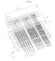
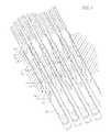
- FIG. 1is a cross-sectional view of a spring contact assembly of the present invention
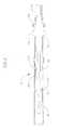
- FIG. 2is a cross-sectional detail view of the terminal design of the plunger of the spring contact assembly of FIG. 1 ;
- FIG. 3is a cross-sectional view of the terminal of FIG. 2 ;
- FIG. 4is a detail view of various contact tip designs of the spring contact assembly of FIG. 1 .
- FIG. 1illustrates a plurality of exemplary spring contact assemblies 10 of the present invention.
- Each spring contact assembly 10includes a first contact member 12 and a second contact member 14 .
- Contact members 12 and 14have a flat configuration and partially overlap one another. The overlapping portions 16 and 18 respectively are positioned within a compression spring 20 .
- compression spring 20has reduced diameter end coils 22 and center coils 24 .
- Contact member 12has a contact tip 26 positioned at an end of the contact member opposite from overlapping portion 16 .
- Contact member 14has a terminal end 28 opposite from overlapping portion 18 . Terminal end 28 is for retaining the spring contact assembly within receptacle 30 .
- receptacles 30There are a plurality of receptacles 30 positioned within a probe plate 32 and the spring contact assemblies 10 are positioned within holes 34 drilled through top plate 36 and a plurality of intermediate plates 38 positioned between top plate 36 and probe plate 32 . It is to be understood that this is only exemplary of a configuration of a fixture 40 for use with the spring contact assemblies 10 . Similarly, the fixture 40 could constitute a socket or housing for other test applications and have an array of receptacles for spring contact assemblies.
- Contact members 12 and 14have a flat configuration and are retained within the cylindrical receptacle 30 by terminal end 28 .
- terminal end 28have a series of tapered cam surfaces 42 and 44 (two are shown) to facilitate retention of the spring contact assembly within the receptacle 30 .
- Tapered cam surface 42provides a lead-end angle on the tail 46 of terminal end 28 which extends to a sharp rear angle 48 .
- Tapered cam surface 44also extends to a sharp rear angle 50 .
- tapered cam surface 42engages a first detent 52 allowing the terminal end 28 to flex inwardly as the angle cam surface rides over the first detent 52 and flex back outwardly as sharp rear angle 48 passes the first detent 52 .
- Tapered cam angle 42continues into a receptacle and similarly flexes and passes over a second detent 54 . While tapered cam surface 42 passes over detent 54 tapered, cam surface 44 similarly passes over first detent 52 flexing the terminal end until sharp rear angle 50 passes over first detent 52 .
- the spacing between first and second rear anglesis similar to the spacing between first and second detents.
- the design of the terminal endis formed to allow the contact assembly to be inserted into the receptacle with minimal force but requires a much more significant force to remove the terminal from the receptacle.
- the cam surfacesengage one or more detents or other extensions or deformations in the receptacle that hold the flat contact member in place.
- Contact member 14includes a flange 56 which engages the end 58 of receptacle 30 . Flange 56 prevents the contact member 14 from being further inserted into the receptacle. Contact member 14 further includes a wider spring flange 60 for receipt of end coils 22 of compression spring 20 .
- contact member 12also includes a spring flange 60 for retention of end coils 22 and can have a variety of different geometrical three dimensional shape contact tips 26 .
- Tip 26 acan be a baloney style tip which is a rounded tip from side-to-side and front to back.
- Tip 26 bis “U” or forked shaped by removing portions of the tip on either side and the front and the back while forming a “U” or fork shaped upper surface.
- Tip 26 cis “V” shaped and includes bending a “V” along the end length of the contact member.
- Tip 26 dis “S” shaped which is formed by stamping a “T” shaped end and folding the ends into an “S” shape.
- Tip 26 eis a “C” shape which is formed by stamping initially an “L” shape on the end and folding the end of the “L” over into the “U” shape. Although a number of three dimensional tip configurations are illustrated, it is to be understood that a number of geometrical configurations are contemplated herein.
- spring contact assembly 10is illustrated with respect to two contact members 12 and 14 wherein contact member 14 has a terminal end positioned within receptacle 30 .
- a novel terminal design for a spring contact assemblycan include a configuration where a flat plunger is retained within a cylindrical barrel having a spring positioned within the barrel.
- the barrelcan be cylindrical or can be rectangular for receipt of a flat contact member which also can be referred to as a plunger.
Landscapes
- Physics & Mathematics (AREA)
- General Physics & Mathematics (AREA)
- Measuring Leads Or Probes (AREA)
Abstract
Description
Claims (20)
Priority Applications (3)
| Application Number | Priority Date | Filing Date | Title |
|---|---|---|---|
| US12/968,023US8710856B2 (en) | 2010-01-15 | 2010-12-14 | Terminal for flat test probe |
| PCT/US2010/061370WO2011087763A1 (en) | 2010-01-15 | 2010-12-20 | Terminal for flat test probe |
| TW099145850ATWI449917B (en) | 2010-01-15 | 2010-12-24 | Compliant contact assembly, combination of a flat contact member and a receptacle and flat test probe |
Applications Claiming Priority (2)
| Application Number | Priority Date | Filing Date | Title |
|---|---|---|---|
| US29562310P | 2010-01-15 | 2010-01-15 | |
| US12/968,023US8710856B2 (en) | 2010-01-15 | 2010-12-14 | Terminal for flat test probe |
Publications (2)
| Publication Number | Publication Date |
|---|---|
| US20110175636A1 US20110175636A1 (en) | 2011-07-21 |
| US8710856B2true US8710856B2 (en) | 2014-04-29 |
Family
ID=44277174
Family Applications (1)
| Application Number | Title | Priority Date | Filing Date |
|---|---|---|---|
| US12/968,023Expired - Fee RelatedUS8710856B2 (en) | 2010-01-15 | 2010-12-14 | Terminal for flat test probe |
Country Status (3)
| Country | Link |
|---|---|
| US (1) | US8710856B2 (en) |
| TW (1) | TWI449917B (en) |
| WO (1) | WO2011087763A1 (en) |
Cited By (5)
| Publication number | Priority date | Publication date | Assignee | Title |
|---|---|---|---|---|
| US20160025775A1 (en)* | 2014-07-23 | 2016-01-28 | Foxconn Interconnect Technology Limited | Electrical connector and contacts thereof |
| US20180013222A1 (en)* | 2016-07-11 | 2018-01-11 | Alps Electric Co., Ltd. | Spring contact, socket including spring contact, and method for manufacturing spring contact |
| US10014604B2 (en)* | 2016-07-11 | 2018-07-03 | Apls Electric Co., Ltd. | Spring contact and socket including spring contact |
| US10161963B2 (en) | 2015-08-17 | 2018-12-25 | Chaojiong Zhang | Electrical contact and testing apparatus |
| US20190346485A1 (en)* | 2016-11-30 | 2019-11-14 | Nidec Read Corporation | Contact terminal, inspection jig, and inspection device |
Families Citing this family (7)
| Publication number | Priority date | Publication date | Assignee | Title |
|---|---|---|---|---|
| US8907694B2 (en)* | 2009-12-17 | 2014-12-09 | Xcerra Corporation | Wiring board for testing loaded printed circuit board |
| SG11201406561XA (en)* | 2012-04-13 | 2014-11-27 | Capital Formation Inc | Test probe assembly and related methods |
| JP6404008B2 (en)* | 2014-06-23 | 2018-10-10 | 株式会社日本マイクロニクス | Electrical contact and electrical connection device |
| CN108663553B (en)* | 2017-03-29 | 2022-01-25 | 上海中船电气有限公司 | Contact type semiconductor material testing head |
| US11454650B2 (en)* | 2018-07-18 | 2022-09-27 | Nidec-Read Corporation | Probe, inspection jig, inspection device, and method for manufacturing probe |
| DE102019107736B4 (en)* | 2019-03-26 | 2024-07-04 | Energybox Ltd. | Measuring equipment and measuring method |
| KR102235344B1 (en)* | 2020-12-31 | 2021-04-05 | 황동원 | Contact pin, and a spring contact and test socket with the same for high speed signal ic test |
Citations (16)
| Publication number | Priority date | Publication date | Assignee | Title |
|---|---|---|---|---|
| US2392438A (en) | 1940-05-02 | 1946-01-08 | Charles E Wade | Electrical connector |
| US5009613A (en)* | 1990-05-01 | 1991-04-23 | Interconnect Devices, Inc. | Spring contact twister probe for testing electrical printed circuit boards |
| US5444387A (en) | 1987-04-17 | 1995-08-22 | Everett Charles Technologies, Inc. | Test module hanger for test fixtures |
| US20010039128A1 (en)* | 2000-05-02 | 2001-11-08 | Masaru Tateishi | Method of connecting IC package to IC contactor with weaker force and IC contactor for such method |
| US20010049213A1 (en)* | 1997-12-17 | 2001-12-06 | Paul J.M. Potters | Electrical connector with floating terminals and terminal thereof |
| US6462567B1 (en)* | 1999-02-18 | 2002-10-08 | Delaware Capital Formation, Inc. | Self-retained spring probe |
| US20040053540A1 (en)* | 2002-09-12 | 2004-03-18 | Jerry Wu | Electrical connector and method of assembling the same |
| US7253647B2 (en)* | 2004-05-17 | 2007-08-07 | Chae Yoon Lee | Probe for high electric current |
| US20070290703A1 (en) | 1998-08-27 | 2007-12-20 | The Micromanipulator Company, Inc. | High Resolution Analytical Probe Station |
| US20070296436A1 (en)* | 2006-06-01 | 2007-12-27 | Rika Denshi America, Inc. | Electrical test probes with a contact element, methods of making and using the same |
| US20080001613A1 (en) | 2006-06-29 | 2008-01-03 | January Kister | Probe skates for electrical testing of convex pad topologies |
| US20090075529A1 (en)* | 2007-09-18 | 2009-03-19 | Johnston Charles J | Spring contact assembly |
| US20090189622A1 (en)* | 2005-10-14 | 2009-07-30 | Yin Leong Tan | Probe For Testing Integrated Circuit Devices |
| US20100244875A1 (en)* | 2009-03-27 | 2010-09-30 | Scott Chabineau-Lovgren | Scrub inducing compliant electrical contact |
| US8052491B2 (en)* | 2009-07-14 | 2011-11-08 | Hon Hai Precision Ind. Co., Ltd. | Electrical contact having upper contact with thickened base portion |
| US8105119B2 (en)* | 2009-01-30 | 2012-01-31 | Delaware Capital Formation, Inc. | Flat plunger round barrel test probe |
Family Cites Families (2)
| Publication number | Priority date | Publication date | Assignee | Title |
|---|---|---|---|---|
| TWM317015U (en)* | 2007-01-25 | 2007-08-11 | Global Master Tech Co Ltd | Test probe |
| TWM333565U (en)* | 2007-10-30 | 2008-06-01 | Ru-Fu Li | Test probe |
- 2010
- 2010-12-14USUS12/968,023patent/US8710856B2/ennot_activeExpired - Fee Related
- 2010-12-20WOPCT/US2010/061370patent/WO2011087763A1/enactiveApplication Filing
- 2010-12-24TWTW099145850Apatent/TWI449917B/ennot_activeIP Right Cessation
Patent Citations (16)
| Publication number | Priority date | Publication date | Assignee | Title |
|---|---|---|---|---|
| US2392438A (en) | 1940-05-02 | 1946-01-08 | Charles E Wade | Electrical connector |
| US5444387A (en) | 1987-04-17 | 1995-08-22 | Everett Charles Technologies, Inc. | Test module hanger for test fixtures |
| US5009613A (en)* | 1990-05-01 | 1991-04-23 | Interconnect Devices, Inc. | Spring contact twister probe for testing electrical printed circuit boards |
| US20010049213A1 (en)* | 1997-12-17 | 2001-12-06 | Paul J.M. Potters | Electrical connector with floating terminals and terminal thereof |
| US20070290703A1 (en) | 1998-08-27 | 2007-12-20 | The Micromanipulator Company, Inc. | High Resolution Analytical Probe Station |
| US6462567B1 (en)* | 1999-02-18 | 2002-10-08 | Delaware Capital Formation, Inc. | Self-retained spring probe |
| US20010039128A1 (en)* | 2000-05-02 | 2001-11-08 | Masaru Tateishi | Method of connecting IC package to IC contactor with weaker force and IC contactor for such method |
| US20040053540A1 (en)* | 2002-09-12 | 2004-03-18 | Jerry Wu | Electrical connector and method of assembling the same |
| US7253647B2 (en)* | 2004-05-17 | 2007-08-07 | Chae Yoon Lee | Probe for high electric current |
| US20090189622A1 (en)* | 2005-10-14 | 2009-07-30 | Yin Leong Tan | Probe For Testing Integrated Circuit Devices |
| US20070296436A1 (en)* | 2006-06-01 | 2007-12-27 | Rika Denshi America, Inc. | Electrical test probes with a contact element, methods of making and using the same |
| US20080001613A1 (en) | 2006-06-29 | 2008-01-03 | January Kister | Probe skates for electrical testing of convex pad topologies |
| US20090075529A1 (en)* | 2007-09-18 | 2009-03-19 | Johnston Charles J | Spring contact assembly |
| US8105119B2 (en)* | 2009-01-30 | 2012-01-31 | Delaware Capital Formation, Inc. | Flat plunger round barrel test probe |
| US20100244875A1 (en)* | 2009-03-27 | 2010-09-30 | Scott Chabineau-Lovgren | Scrub inducing compliant electrical contact |
| US8052491B2 (en)* | 2009-07-14 | 2011-11-08 | Hon Hai Precision Ind. Co., Ltd. | Electrical contact having upper contact with thickened base portion |
Non-Patent Citations (1)
| Title |
|---|
| International Search Report and Written Opinion for International Application No. PCT/US2010/061370, mailed Feb. 16, 2011, 8 pages. |
Cited By (8)
| Publication number | Priority date | Publication date | Assignee | Title |
|---|---|---|---|---|
| US20160025775A1 (en)* | 2014-07-23 | 2016-01-28 | Foxconn Interconnect Technology Limited | Electrical connector and contacts thereof |
| US10422816B2 (en)* | 2014-07-23 | 2019-09-24 | Foxconn Interconnect Technology Limited | Electrical connector and contacts thereof |
| US10161963B2 (en) | 2015-08-17 | 2018-12-25 | Chaojiong Zhang | Electrical contact and testing apparatus |
| US20180013222A1 (en)* | 2016-07-11 | 2018-01-11 | Alps Electric Co., Ltd. | Spring contact, socket including spring contact, and method for manufacturing spring contact |
| US10014604B2 (en)* | 2016-07-11 | 2018-07-03 | Apls Electric Co., Ltd. | Spring contact and socket including spring contact |
| US10033125B2 (en)* | 2016-07-11 | 2018-07-24 | Alps Electric Co., Ltd. | Spring contact, socket including spring contact, and method for manufacturing spring contact |
| US20190346485A1 (en)* | 2016-11-30 | 2019-11-14 | Nidec Read Corporation | Contact terminal, inspection jig, and inspection device |
| US10656179B2 (en)* | 2016-11-30 | 2020-05-19 | Nidec-Read Corporation | Contact terminal, inspection jig, and inspection device |
Also Published As
| Publication number | Publication date |
|---|---|
| TW201140069A (en) | 2011-11-16 |
| WO2011087763A1 (en) | 2011-07-21 |
| TWI449917B (en) | 2014-08-21 |
| US20110175636A1 (en) | 2011-07-21 |
Similar Documents
| Publication | Publication Date | Title |
|---|---|---|
| US8710856B2 (en) | Terminal for flat test probe | |
| US7862391B2 (en) | Spring contact assembly | |
| EP2836847B1 (en) | Test probe assembly and related methods | |
| KR101012712B1 (en) | Compliant Electrical Interconnect and Electrical Contact Probes | |
| EP1510827B1 (en) | Spring probe | |
| US8324919B2 (en) | Scrub inducing compliant electrical contact | |
| US20100267291A1 (en) | Swaging process for improved compliant contact electrical test performance | |
| US6462567B1 (en) | Self-retained spring probe | |
| US20100197176A1 (en) | Flat plunger round barrel test probe | |
| KR101894965B1 (en) | Probe pin and ic socket | |
| US20100007365A1 (en) | Socket for double ended probe, double ended probe, and probe unit | |
| KR101715738B1 (en) | A Test Socket | |
| HK1054984B (en) | Self-retained spring probe |
Legal Events
| Date | Code | Title | Description |
|---|---|---|---|
| AS | Assignment | Owner name:DELAWARE CAPITAL FORMATION, INC., DELAWARE Free format text:ASSIGNMENT OF ASSIGNORS INTEREST;ASSIGNORS:SWART, MARK A.;SNYDER, KENNETH R.;REEL/FRAME:025702/0808 Effective date:20101115 | |
| AS | Assignment | Owner name:SILICON VALLEY BANK, AS ADMINISTRATIVE AGENT, CALI Free format text:SECURITY AGREEMENT;ASSIGNORS:LTX-CREDENCE CORPORATION;EVERETT CHARLES TECHNOLOGIES LLC;REEL/FRAME:032086/0476 Effective date:20131127 | |
| STCF | Information on status: patent grant | Free format text:PATENTED CASE | |
| AS | Assignment | Owner name:XCERRA CORPORATION, MASSACHUSETTS Free format text:CHANGE OF NAME;ASSIGNOR:LTX-CREDENCE CORPORATION;REEL/FRAME:033032/0768 Effective date:20140520 | |
| AS | Assignment | Owner name:LTX-CREDENCE CORPORATION, MASSACHUSETTS Free format text:ASSIGNMENT OF ASSIGNORS INTEREST;ASSIGNOR:DELAWARE CAPITAL FORMATION, INC.;REEL/FRAME:033091/0639 Effective date:20131122 | |
| AS | Assignment | Owner name:SILICON VALLEY BANK, AS ADMINISTRATIVE AGENT, CALI Free format text:SECURITY AGREEMENT;ASSIGNORS:XCERRA CORPORATION;EVERETT CHARLES TECHNOLOGIES LLC;REEL/FRAME:034660/0188 Effective date:20141215 Owner name:EVERETT CHARLES TECHNOLOGIES LLC, MASSACHUSETTS Free format text:RELEASE OF SECURITY INTEREST IN UNITED STATES PATENTS;ASSIGNOR:SILICON VALLEY BANK, AS ADMINISTRATIVE AGENT;REEL/FRAME:034660/0394 Effective date:20141215 Owner name:XCERRA CORPORATION, MASSACHUSETTS Free format text:RELEASE OF SECURITY INTEREST IN UNITED STATES PATENTS;ASSIGNOR:SILICON VALLEY BANK, AS ADMINISTRATIVE AGENT;REEL/FRAME:034660/0394 Effective date:20141215 | |
| AS | Assignment | Owner name:SILICON VALLEY BANK, AS ADMINISTRATIVE AGENT, CALI Free format text:CORRECTIVE ASSIGNMENT TO CORRECT THE INCORRECT PATENT NUMBER 7261561 AND REPLACE WITH PATENT NUMBER 7231561 PREVIOUSLY RECORDED ON REEL 034660 FRAME 0188. ASSIGNOR(S) HEREBY CONFIRMS THE SECURITY AGREEMENT;ASSIGNORS:XCERRA CORPORATION;EVERETT CHARLES TECHNOLOGIES LLC;REEL/FRAME:037824/0372 Effective date:20141215 | |
| MAFP | Maintenance fee payment | Free format text:PAYMENT OF MAINTENANCE FEE, 4TH YEAR, LARGE ENTITY (ORIGINAL EVENT CODE: M1551) Year of fee payment:4 | |
| AS | Assignment | Owner name:DEUTSCHE BANK AG NEW YORK BRANCH, AS COLLATERAL AGENT, NEW YORK Free format text:PATENT SECURITY AGREEMENT;ASSIGNOR:XCERRA CORPORATION;REEL/FRAME:047185/0624 Effective date:20181001 Owner name:DEUTSCHE BANK AG NEW YORK BRANCH, AS COLLATERAL AG Free format text:PATENT SECURITY AGREEMENT;ASSIGNOR:XCERRA CORPORATION;REEL/FRAME:047185/0624 Effective date:20181001 | |
| AS | Assignment | Owner name:DEUTSCHE BANK AG NEW YORK BRANCH, AS COLLATERAL AGENT, NEW YORK Free format text:CORRECTIVE ASSIGNMENT TO CORRECT THE INCORRECT STATEMENT THAT THIS DOCUMENT SERVES AS AN OATH/DECLARATION PREVIOUSLY RECORDED ON REEL 047185 FRAME 0628. ASSIGNOR(S) HEREBY CONFIRMS THE PATENT SECURITY AGREEMENT;ASSIGNOR:XCERRA CORPORATION;REEL/FRAME:047675/0354 Effective date:20181001 Owner name:DEUTSCHE BANK AG NEW YORK BRANCH, AS COLLATERAL AG Free format text:CORRECTIVE ASSIGNMENT TO CORRECT THE INCORRECT STATEMENT THAT THIS DOCUMENT SERVES AS AN OATH/DECLARATION PREVIOUSLY RECORDED ON REEL 047185 FRAME 0628. ASSIGNOR(S) HEREBY CONFIRMS THE PATENT SECURITY AGREEMENT;ASSIGNOR:XCERRA CORPORATION;REEL/FRAME:047675/0354 Effective date:20181001 | |
| FEPP | Fee payment procedure | Free format text:MAINTENANCE FEE REMINDER MAILED (ORIGINAL EVENT CODE: REM.); ENTITY STATUS OF PATENT OWNER: LARGE ENTITY | |
| LAPS | Lapse for failure to pay maintenance fees | Free format text:PATENT EXPIRED FOR FAILURE TO PAY MAINTENANCE FEES (ORIGINAL EVENT CODE: EXP.); ENTITY STATUS OF PATENT OWNER: LARGE ENTITY | |
| STCH | Information on status: patent discontinuation | Free format text:PATENT EXPIRED DUE TO NONPAYMENT OF MAINTENANCE FEES UNDER 37 CFR 1.362 | |
| FP | Lapsed due to failure to pay maintenance fee | Effective date:20220429 | |
| AS | Assignment | Owner name:XCERRA CORPORATION, MASSACHUSETTS Free format text:TERMINATION AND RELEASE OF SECURITY INTEREST IN PATENTS, RECORDED AT REEL 047185, FRAME 0624;ASSIGNOR:DEUTSCHE BANK AG NEW YORK BRANCH, AS AGENT;REEL/FRAME:066762/0811 Effective date:20240209 |