US8709162B2 - Active cooling substrate support - Google Patents
Active cooling substrate supportDownload PDFInfo
- Publication number
- US8709162B2 US8709162B2US11/206,245US20624505AUS8709162B2US 8709162 B2US8709162 B2US 8709162B2US 20624505 AUS20624505 AUS 20624505AUS 8709162 B2US8709162 B2US 8709162B2
- Authority
- US
- United States
- Prior art keywords
- substrate support
- conductive body
- substrate
- support assembly
- cooling
- Prior art date
- Legal status (The legal status is an assumption and is not a legal conclusion. Google has not performed a legal analysis and makes no representation as to the accuracy of the status listed.)
- Active, expires
Links
Images


Classifications
- C—CHEMISTRY; METALLURGY
- C23—COATING METALLIC MATERIAL; COATING MATERIAL WITH METALLIC MATERIAL; CHEMICAL SURFACE TREATMENT; DIFFUSION TREATMENT OF METALLIC MATERIAL; COATING BY VACUUM EVAPORATION, BY SPUTTERING, BY ION IMPLANTATION OR BY CHEMICAL VAPOUR DEPOSITION, IN GENERAL; INHIBITING CORROSION OF METALLIC MATERIAL OR INCRUSTATION IN GENERAL
- C23C—COATING METALLIC MATERIAL; COATING MATERIAL WITH METALLIC MATERIAL; SURFACE TREATMENT OF METALLIC MATERIAL BY DIFFUSION INTO THE SURFACE, BY CHEMICAL CONVERSION OR SUBSTITUTION; COATING BY VACUUM EVAPORATION, BY SPUTTERING, BY ION IMPLANTATION OR BY CHEMICAL VAPOUR DEPOSITION, IN GENERAL
- C23C16/00—Chemical coating by decomposition of gaseous compounds, without leaving reaction products of surface material in the coating, i.e. chemical vapour deposition [CVD] processes
- C23C16/44—Chemical coating by decomposition of gaseous compounds, without leaving reaction products of surface material in the coating, i.e. chemical vapour deposition [CVD] processes characterised by the method of coating
- C23C16/46—Chemical coating by decomposition of gaseous compounds, without leaving reaction products of surface material in the coating, i.e. chemical vapour deposition [CVD] processes characterised by the method of coating characterised by the method used for heating the substrate
- H—ELECTRICITY
- H01—ELECTRIC ELEMENTS
- H01L—SEMICONDUCTOR DEVICES NOT COVERED BY CLASS H10
- H01L21/00—Processes or apparatus adapted for the manufacture or treatment of semiconductor or solid state devices or of parts thereof
- H01L21/67—Apparatus specially adapted for handling semiconductor or electric solid state devices during manufacture or treatment thereof; Apparatus specially adapted for handling wafers during manufacture or treatment of semiconductor or electric solid state devices or components ; Apparatus not specifically provided for elsewhere
- H01L21/683—Apparatus specially adapted for handling semiconductor or electric solid state devices during manufacture or treatment thereof; Apparatus specially adapted for handling wafers during manufacture or treatment of semiconductor or electric solid state devices or components ; Apparatus not specifically provided for elsewhere for supporting or gripping
- C—CHEMISTRY; METALLURGY
- C23—COATING METALLIC MATERIAL; COATING MATERIAL WITH METALLIC MATERIAL; CHEMICAL SURFACE TREATMENT; DIFFUSION TREATMENT OF METALLIC MATERIAL; COATING BY VACUUM EVAPORATION, BY SPUTTERING, BY ION IMPLANTATION OR BY CHEMICAL VAPOUR DEPOSITION, IN GENERAL; INHIBITING CORROSION OF METALLIC MATERIAL OR INCRUSTATION IN GENERAL
- C23C—COATING METALLIC MATERIAL; COATING MATERIAL WITH METALLIC MATERIAL; SURFACE TREATMENT OF METALLIC MATERIAL BY DIFFUSION INTO THE SURFACE, BY CHEMICAL CONVERSION OR SUBSTITUTION; COATING BY VACUUM EVAPORATION, BY SPUTTERING, BY ION IMPLANTATION OR BY CHEMICAL VAPOUR DEPOSITION, IN GENERAL
- C23C16/00—Chemical coating by decomposition of gaseous compounds, without leaving reaction products of surface material in the coating, i.e. chemical vapour deposition [CVD] processes
- C23C16/44—Chemical coating by decomposition of gaseous compounds, without leaving reaction products of surface material in the coating, i.e. chemical vapour deposition [CVD] processes characterised by the method of coating
- C23C16/458—Chemical coating by decomposition of gaseous compounds, without leaving reaction products of surface material in the coating, i.e. chemical vapour deposition [CVD] processes characterised by the method of coating characterised by the method used for supporting substrates in the reaction chamber
- C23C16/4582—Rigid and flat substrates, e.g. plates or discs
- C23C16/4583—Rigid and flat substrates, e.g. plates or discs the substrate being supported substantially horizontally
- C23C16/4586—Elements in the interior of the support, e.g. electrodes, heating or cooling devices
- C—CHEMISTRY; METALLURGY
- C23—COATING METALLIC MATERIAL; COATING MATERIAL WITH METALLIC MATERIAL; CHEMICAL SURFACE TREATMENT; DIFFUSION TREATMENT OF METALLIC MATERIAL; COATING BY VACUUM EVAPORATION, BY SPUTTERING, BY ION IMPLANTATION OR BY CHEMICAL VAPOUR DEPOSITION, IN GENERAL; INHIBITING CORROSION OF METALLIC MATERIAL OR INCRUSTATION IN GENERAL
- C23C—COATING METALLIC MATERIAL; COATING MATERIAL WITH METALLIC MATERIAL; SURFACE TREATMENT OF METALLIC MATERIAL BY DIFFUSION INTO THE SURFACE, BY CHEMICAL CONVERSION OR SUBSTITUTION; COATING BY VACUUM EVAPORATION, BY SPUTTERING, BY ION IMPLANTATION OR BY CHEMICAL VAPOUR DEPOSITION, IN GENERAL
- C23C16/00—Chemical coating by decomposition of gaseous compounds, without leaving reaction products of surface material in the coating, i.e. chemical vapour deposition [CVD] processes
- C23C16/44—Chemical coating by decomposition of gaseous compounds, without leaving reaction products of surface material in the coating, i.e. chemical vapour deposition [CVD] processes characterised by the method of coating
- C23C16/46—Chemical coating by decomposition of gaseous compounds, without leaving reaction products of surface material in the coating, i.e. chemical vapour deposition [CVD] processes characterised by the method of coating characterised by the method used for heating the substrate
- C23C16/463—Cooling of the substrate
- H—ELECTRICITY
- H01—ELECTRIC ELEMENTS
- H01J—ELECTRIC DISCHARGE TUBES OR DISCHARGE LAMPS
- H01J37/00—Discharge tubes with provision for introducing objects or material to be exposed to the discharge, e.g. for the purpose of examination or processing thereof
- H01J37/32—Gas-filled discharge tubes
- H01J37/32431—Constructional details of the reactor
- H01J37/32715—Workpiece holder
- H01J37/32724—Temperature
- H—ELECTRICITY
- H01—ELECTRIC ELEMENTS
- H01L—SEMICONDUCTOR DEVICES NOT COVERED BY CLASS H10
- H01L21/00—Processes or apparatus adapted for the manufacture or treatment of semiconductor or solid state devices or of parts thereof
- H01L21/67—Apparatus specially adapted for handling semiconductor or electric solid state devices during manufacture or treatment thereof; Apparatus specially adapted for handling wafers during manufacture or treatment of semiconductor or electric solid state devices or components ; Apparatus not specifically provided for elsewhere
- H01L21/683—Apparatus specially adapted for handling semiconductor or electric solid state devices during manufacture or treatment thereof; Apparatus specially adapted for handling wafers during manufacture or treatment of semiconductor or electric solid state devices or components ; Apparatus not specifically provided for elsewhere for supporting or gripping
- H01L21/687—Apparatus specially adapted for handling semiconductor or electric solid state devices during manufacture or treatment thereof; Apparatus specially adapted for handling wafers during manufacture or treatment of semiconductor or electric solid state devices or components ; Apparatus not specifically provided for elsewhere for supporting or gripping using mechanical means, e.g. chucks, clamps or pinches
- C—CHEMISTRY; METALLURGY
- C23—COATING METALLIC MATERIAL; COATING MATERIAL WITH METALLIC MATERIAL; CHEMICAL SURFACE TREATMENT; DIFFUSION TREATMENT OF METALLIC MATERIAL; COATING BY VACUUM EVAPORATION, BY SPUTTERING, BY ION IMPLANTATION OR BY CHEMICAL VAPOUR DEPOSITION, IN GENERAL; INHIBITING CORROSION OF METALLIC MATERIAL OR INCRUSTATION IN GENERAL
- C23C—COATING METALLIC MATERIAL; COATING MATERIAL WITH METALLIC MATERIAL; SURFACE TREATMENT OF METALLIC MATERIAL BY DIFFUSION INTO THE SURFACE, BY CHEMICAL CONVERSION OR SUBSTITUTION; COATING BY VACUUM EVAPORATION, BY SPUTTERING, BY ION IMPLANTATION OR BY CHEMICAL VAPOUR DEPOSITION, IN GENERAL
- C23C16/00—Chemical coating by decomposition of gaseous compounds, without leaving reaction products of surface material in the coating, i.e. chemical vapour deposition [CVD] processes
- C23C16/44—Chemical coating by decomposition of gaseous compounds, without leaving reaction products of surface material in the coating, i.e. chemical vapour deposition [CVD] processes characterised by the method of coating
- C23C16/458—Chemical coating by decomposition of gaseous compounds, without leaving reaction products of surface material in the coating, i.e. chemical vapour deposition [CVD] processes characterised by the method of coating characterised by the method used for supporting substrates in the reaction chamber
- C23C16/4582—Rigid and flat substrates, e.g. plates or discs
- C23C16/4583—Rigid and flat substrates, e.g. plates or discs the substrate being supported substantially horizontally
- H—ELECTRICITY
- H01—ELECTRIC ELEMENTS
- H01L—SEMICONDUCTOR DEVICES NOT COVERED BY CLASS H10
- H01L21/00—Processes or apparatus adapted for the manufacture or treatment of semiconductor or solid state devices or of parts thereof
- H01L21/67—Apparatus specially adapted for handling semiconductor or electric solid state devices during manufacture or treatment thereof; Apparatus specially adapted for handling wafers during manufacture or treatment of semiconductor or electric solid state devices or components ; Apparatus not specifically provided for elsewhere
- H01L21/67005—Apparatus not specifically provided for elsewhere
- H01L21/67011—Apparatus for manufacture or treatment
- H01L21/67017—Apparatus for fluid treatment
- H01L21/67063—Apparatus for fluid treatment for etching
- H01L21/67069—Apparatus for fluid treatment for etching for drying etching
- H—ELECTRICITY
- H01—ELECTRIC ELEMENTS
- H01L—SEMICONDUCTOR DEVICES NOT COVERED BY CLASS H10
- H01L21/00—Processes or apparatus adapted for the manufacture or treatment of semiconductor or solid state devices or of parts thereof
- H01L21/67—Apparatus specially adapted for handling semiconductor or electric solid state devices during manufacture or treatment thereof; Apparatus specially adapted for handling wafers during manufacture or treatment of semiconductor or electric solid state devices or components ; Apparatus not specifically provided for elsewhere
- H01L21/67005—Apparatus not specifically provided for elsewhere
- H01L21/67011—Apparatus for manufacture or treatment
- H01L21/67098—Apparatus for thermal treatment
- H01L21/67103—Apparatus for thermal treatment mainly by conduction
Definitions
- Embodiments of the inventiongenerally provide a substrate support utilized in flat panel substrate processing.
- Liquid crystal displays or flat panel displaysare commonly used for active matrix displays such as computer and television monitors, personal digital assistants (PDAs), and cell phones, as well as solar cells and the like.
- a flat panel displaycomprises two glass plates having a layer of liquid crystal material sandwiched therebetween. At least one of the glass plates includes at least one conductive film disposed thereon that is coupled to a power supply. Power supplied to the conductive film from the power supply changes the orientation of the crystal material, creating a pattern such as texts or graphics on the flat panel displays.
- Substrates utilized for flat panel fabricationare large in size, often exceeding 300 mm ⁇ 400 mm, and are envisioned up to and beyond 4 square meters in surface area.
- the substrate supports utilized to process large area substratesare proportionately large to accommodate the large surface area of the substrate.
- FIG. 1is a schematic cross-sectional view of a CVD process chamber 2 having a support plate 18 and a susceptor 22 disposed therein to support a substrate 12 (not to scale). Reactive precursor gases flowing into a diffuser plate 16 through a gas inlet 14 near the top of the process chamber 2 are excited to form a layer of material on the surface of the substrate 12 that is positioned on a temperature controlled substrate support or susceptor 22 .
- a support plate 18 coupled to a support shaft 20 to support the susceptor 22is typically made of a single rectangular plate of ceramic material, such as aluminum oxide, and closely covers the area of the susceptor 22 .
- the susceptor 22 for a CVD chamberhistorically has been made of a single rectangular plate of aluminum and is typically heated by an embedded heater (not shown) with thermocouples and energy supplied from a power source 24 .
- the heatercan also be positioned to the back side of the susceptor 22 or clamped onto the susceptor 22 by a clamp plate.
- the substrate support of the process chamber 2may be heated from room temperature to a high temperature of less than 500° C., and the susceptor 22 can deflect and “droop” without adequate support.
- the ceramic material of the support plate 18has been used to support the susceptor 22 made of ductile aluminum.
- ceramicis a relatively poor thermal conductor and, thus, demonstrates a temperature gradient between a hotter upper surface of the support plate 18 that contacts the heated susceptor and a cooler lower surface of the support plate 18 and as a result, the support plate 18 deflects downwardly at its outer perimeter.
- a substrate supported by the susceptoris prone to conform to the susceptor and, thus, also deflects.
- the vertical spacing between the diffuser plate 16 and the substrate 12varies between a central portion of the substrate 12 having a distance 34 from the diffuser plate 16 .
- a greater distance 36 resulting from large degree of deflectionis located near it perimeter.
- the difference in the vertical spacingi.e., substrate deflection distance greatly decreases uniformity of the deposited films disposed on the large area substrate.
- the energy from the plasmaafter striking a plasma inside a PEPVD chamber, the energy from the plasma also creates heat directed toward the substrate and the substrate support, e.g., the susceptor. Therefore, there is a problem of a temporal temperature increase or spike (e.g., about 30-50° C. increase or 20%-30% temperature increase from 150° C.) for the processing substrate disposed on the susceptor.
- a temporal temperature increase or spikee.g., about 30-50° C. increase or 20%-30% temperature increase from 150° C.
- Such drastic temperature variationneeds to be controlled in order to maintain a constant temperature on the substrate being processed.
- cooling of the susceptor of a process chamberis also needed after processing and during remote plasma cleaning, RF assist cooling, and/or chamber part cleaning and maintenance.
- a substrate support assemblyadapted to support a large area substrate inside a process chamber includes a thermally conductive body, a substrate support surface on the surface of the thermally conductive body and adapted to support the large area substrate thereon, one or more heating elements embedded within the thermally conductive body, and one or more cooling channels embedded within the thermally conductive body above the one or more heating elements.
- a substrate support assemblymay include one or more cooling channels embedded within the thermally conductive body and looped around the positions of the one or more heating elements in a spiral or vortex configuration.
- the one or more cooling channelsinclude in-flow loops and out-flow loops. The in-flow loops and/or the out-flow loops may each be configured in a spiral configuration within the thermally conductive body.
- the neighboring cooling channelsinclude cooling fluids flowing in opposite in-flow and out-flow directions.
- a process chamberincluding a chamber body, a gas distribution plate assembly, and a substrate support assembly for supporting a large area substrate thereon.
- the substrate support assemblymay include a thermally conductive body, a substrate support surface on the surface of the thermally conductive body and adapted to support the large area glass substrate thereon, one or more heating elements embedded within the thermally conductive body, and one or more cooling channels embedded within the thermally conductive body above the one or more heating elements and positioned around the one or more heating elements in a spiral or vortex configuration.
- a method for maintaining the temperature of a large area substrate inside a process chamberincludes positioning the large area substrate on a substrate support surface of a substrate support assembly of the process chamber, flowing a gaseous cooling material constantly inside the one or more cooling channels at a constant flow rate, and maintaining the temperature of the large area substrate by adjusting the heating power of the one or more heating elements.
- FIG. 1depicts a schematic sectional view of a substrate support in a CVD process chamber.
- FIG. 2depicts a schematic sectional view of one embodiment of a process chamber having a substrate support assembly of the invention.
- FIG. 3Ais a planar-view of a substrate support body according to one embodiment of the invention.
- FIG. 3Bis another planar view of a substrate support body according to another embodiment of the invention.
- FIG. 4Ais a planar view of a substrate support body according to one embodiment of the invention.
- FIG. 4Bis another planar view of a substrate support body according to another embodiment of the invention.
- FIG. 4Cis still another planar view of a substrate support body according to another embodiment of the invention.
- FIG. 5is a cross-sectional view of one embodiment of a substrate support body of the invention.
- FIG. 6is a flow diagram of one embodiment of a method for controlling the temperature of a substrate within a process chamber.
- FIG. 2illustrates an exemplary process chamber 100 according to one embodiment of the invention.
- the inventionis illustratively described below in reference to a plasma enhanced chemical vapor deposition process chamber for processing large area substrates, such as those available from AKT, a division of Applied Materials, Inc., Santa Clara, Calif.
- AKTa plasma enhanced chemical vapor deposition process chamber
- the inventionhas utility in other system configurations such as physical vapor deposition systems, ion implant systems, etch systems, chemical vapor deposition systems, and any other system in which controlling the temperature of a substrate on a substrate support within a process chamber is desired.
- the process chamber 100includes a chamber body 102 having walls 106 and a bottom 108 that partially define a process volume 140 .
- the process volume 140is typically accessed through a port and a valve (not shown) to facilitate movement of a substrate 112 , such as a large area glass substrate, into and out of the process chamber 100 .
- the walls 106support a lid assembly 110 that contains a pumping plenum 114 that couples the process volume 140 to an exhaust port (that includes various pumping components, not shown) for exhausting any gases and process by-products out of the process chamber 100 .
- the process chamber 100is usually coupled to one or more supply sources 104 for delivery of one or more source compounds and/or precursors, e.g., a silicon-containing compound supply source, a oxygen-containing compound supply source, a hydrogen gas supply source, a carbon-containing compound supply source, among others, and/or combinations thereof.
- a silicon-containing compound supply sourcee.g., a silicon-containing compound supply source, a oxygen-containing compound supply source, a hydrogen gas supply source, a carbon-containing compound supply source, among others, and/or combinations thereof.
- a substrate support assembly 138is generally disposed on the bottom of the chamber body 102 .
- the support assembly 138generally is grounded such that RF power supplied by a power source 122 to a gas distribution plate assembly 118 positioned between the lid assembly 110 and the substrate support assembly 138 (or other electrode positioned within or near the lid assembly 110 of the process chamber 100 ) may excite gases, source compounds, and/or precursors present in the process volume 140 between the substrate support assembly 138 and the gas distribution plate assembly 118 .
- the RF power from the power source 122is generally selected commensurate with the size of the substrate 112 to drive the chemical vapor deposition process.
- a RF power of about 400 W or largercan be applied to the power source 122 to generate an electric field in the process volume 140 .
- a power density of about 0.2 watts/cm 2 or largersuch as between about 0.2 watts/cm 2 to about 0.8 watt/cm 2 , or about 0.45 watts/cm 2 , can be used to be compatible with a low temperature substrate deposition method of the invention.
- the power source 122 and matching network(not shown) create and sustain a plasma of the process gases from the precursor gases in the process volume 140 .
- Preferably high frequency RF power of 13.56 MHzcan be used, but this is not critical and lower frequencies can also be used.
- the walls of the chambercan be protected by covering with a ceramic material or anodized aluminum material.
- the substrate support assembly 138is coupled to a shaft 142 and connected to a lift system (not shown) for moving the substrate support assembly 138 between an elevated processing position (as shown) and a lowered substrate transfer position.
- the shaft 142additionally provides a conduit for electrical and thermocouple leads between the substrate support assembly 138 and other components of the process chamber 100 .
- a bellows 146is coupled to the substrate support assembly 138 to provide a vacuum seal between the process volume 140 and the atmosphere outside the process chamber 100 and facilitate vertical movement of the substrate support assembly 138 .
- the lift system of the substrate support assembly 138is generally adjusted such that a spacing between the substrate 112 and the gas distribution plate assembly 118 is optimized, such as at about 400 mils or larger, during processing. The ability to adjust the spacing enables the process to be optimized over a wide range of deposition conditions, while maintaining the required film uniformity over the area of a large substrate.
- the substrate support assembly 138includes a conductive body 124 having a substrate support surface 134 to support the substrate 112 thereon within the process volume 140 during substrate processing.
- the conductive body 124can be made of a metal or metal alloy material which provides thermal conductivity. In one embodiment, the conductive body 124 is made of an aluminum material. However, other suitable materials can also be used.
- the substrate support assembly 138additionally supports a shadow frame 148 circumscribing the substrate 112 disposed on the substrate supporting surface 134 during substrate processing.
- the shadow frame 148prevents deposition at the edge of the substrate 112 and the substrate support assembly 138 so that the substrate 112 does not stick to the support assembly 138 .
- the shadow frame 148is generally positioned alongside inner wall of the chamber body 102 when the substrate support assembly 138 is in a lower non-processing position (not shown).
- the shadow frame 148can be engaged and aligned to the conductive body 124 of the substrate support assembly 138 , when the substrate support assembly 138 is in an upper processing position, as shown in FIG. 2 , by matching one or more alignment grooves on the shadow frame 148 with one or more alignment pins 202 .
- the one or more alignment pins 202are adapted to pass through one or more alignment pin holes 204 located on and near the perimeter of the conductive body 124 .
- the one or more alignment pins 202may be optionally supported by a support pin plate 234 to be movable with the conductive body 124 during substrate loading and unloading.
- the substrate support assembly 138 which is temperature controlledmay also include one or more electrodes and/or heating elements 132 coupled to a power source 174 to controllably heat the substrate support assembly 138 and the substrate 112 positioned thereon to a predetermined temperature range, e.g., a set point temperature of about 100° C. or higher.
- the one or more heating elements 132are embedded within the conductive body 124 .
- FIGS. 3A-3Billustrate planar views of the one or more heating elements 132 disposed in the conductive body 124 , according to one or more aspects of the invention.
- the heating element 132may enter the conductive body 124 through the shaft 142 , loop around a center region of the conductive body 124 in one or more inner loops and around an outer perimeter of the conductive body 124 in one or more outer loops, and exit through the shaft 142 , such that the one or more heating elements 132 is embedded across the dimension of the conductive body 124 .
- thermocouplescan be used within the substrate support assembly 138 .
- two thermocouplesare used, such as one for the center region and one for the outer perimeter of the conductive body 124 .
- other heater lines or channel configurationscan also be used.
- the one or more heating elements 132can also be positioned on the back side of the conductive body 124 or clamped onto the conductive body 124 by a clamp plate. The one or more heating elements 132 may be resistively heated or by other heating means to a predetermined temperature of about 100° C. or higher.
- the substrate support assembly 138may include additional mechanisms adapted to retain and align the substrate 112 .
- the conductive body 124may include one or more substrate support pin holes 224 for a plurality of substrate support pins 222 therethrough and adapted to support the substrate 112 a small distance above the conductive body 124 .
- the substrate support pins 222can be positioned near the perimeter of the substrate 112 to facilitate the placement or removal of the substrate 112 by a transfer robot or other transfer mechanism disposed exterior to the process chamber 100 without interfering with the transfer robot.
- the substrate support pins 222can be made of an insulating material, such as ceramic materials, anodized aluminum oxides materials, among others, to provide electrical insulation during substrate processing and still being thermally conductive.
- the substrate support pins 222may be optionally supported by the support pin plate 234 such that the substrate support pins 222 are movable within the substrate support assembly 138 for lifting the substrate 112 during substrate loading and unloading.
- the substrate support pins 222may be secured to the chamber bottom and the conductive body 124 is vertically movable for the substrate support pins 222 to pass through.
- At least one outer loop of the heating element 132is configured to align to an outer perimeter of the substrate 122 when the substrate 112 is placed onto the substrate support surface 134 of the conductive body 124 .
- the position of the at least one outer loop of the heating element 132may be configured to enclose the perimeter of the substrate 112 without interfering with the positions of one or more pin holes on the conductive body 124 , e.g., the substrate support pin holes 224 or the alignment pin holes 204 .
- one embodiment of the inventionprovides that the at least one outer loop of the heating element 132 is positioned to surround the outer edges of the substrate 112 .
- the at least one outer loop of the heating element 132is positioned around the one or more substrate support pin holes 224 and farther away from the center of the conductive body 124 without interfering with the positions of the one or more substrate support pin holes 224 , thus, the positions of the substrate support pins 222 for supporting the edges of the substrate 112 .
- another embodiment of the inventionprovides that the at least one outer loop of the heating element 132 is positioned between the one or more substrate support pin holes 224 and the outer edges of the conductive body 124 in order to provide heating to the edges and perimeter of the substrate 112 .
- the substrate support assembly 138further includes one or more cooling channels 136 embedded within the conductive body 124 .
- the one or more cooling channels 136are configured to maintain temperature control and compensate temperature variation which may occur during substrate processing, such as a temperature increase or spike when a RF plasma is generated inside the process chamber 100 .
- the diameter of the cooling channel 136is not limited and can be any suitable diameters, such as between about 1 mm to about 15 mm, e.g., about 9 mm.
- the cooling channel 136can be made of a metal or metal alloy material which provides thermal conductivity.
- the cooling channel 136is made of a stainless steel material. However, other suitable materials or configurations can also be used.
- the cooling channels 136are adapted to flow cooling fluids therein, such as gaseous materials, water, coolants, and other suitable cooling gases or liquid materials therein.
- gaseous materialsare used.
- Suitable gaseous materialsmay include clean dry air, compressed air, filtered air, nitrogen gas, hydrogen gas, inert gas (e.g., argon gas, helium gas, etc.), and other gases.
- Flowing a gaseous material inside the one or more cooling channels 136is beneficial than flowing cooling water therein, even though cooling water can be used to advantage, since the gaseous material can provide cooling capability at a broader temperature range without the possibility of moisture leak to affect the quality of the deposited film on the processing substrate and chamber components.
- the gaseous material of about 10° C. to about 25° C.can be used to flow into the one or more cooling channels 136 and provide temperature cooling control from room temperature up to a high temperature of about 200° C. or higher, whereas cooling water generally operates at between about 20° C. to about 100° C.
- the cooling fluids flowing inside the cooling channels 136can be operated at a controlled flow rate to control cooling efficiency during substrate processing when the substrate 112 is heated by the heating element 132 and/or during chamber idle time.
- a pressure of about 25 psi to about 100 psi, such as about 50 psican be used to flow a gaseous cooling material.
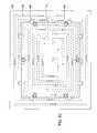
- FIGS. 4A-4Cillustrate exemplary configurations of the heating element 132 and the cooling channels 136 disposed in the conductive body 124 of the substrate support assembly 138 .
- cooling fluidmay be flown into the conductive body 124 through one or more in-flow cooling channels extending from the central shaft toward the conductive body 124 in a flow direction 400 A, where the one or more in-flow cooling channels extend into and out toward the perimeter of the conductive body 124 in a spiral configuration or vortex shape.
- the cooling fluidis flown from the in-flow cooling channels to one or more out-flow cooling channels extending toward the central shaft in a flow direction 400 B, where the one or more out-flow cooling channels extend out of the conductive body 124 in a spiral configuration.
- the cooling channels 136may be configured, in one embodiment, in a double spiral configuration, one spiral in-flow and another spiral out-flow as indicated by the flow directions 400 A and 400 B.
- the neighboring loops or channels of the cooling channels 136are configured for flowing the cooling fluid in opposite directions, as indicated by the flow directions 400 A and 400 B.
- FIG. 4Bdemonstrates another exemplary cooling channels and heating element of the invention.
- the cooling channels 136may enter the conductive body 124 through the shaft 142 and are configured to form into one or more inner cooling loops 436 A to loop around the one or more inner loops of the heating element 132 .
- the cooling channels 136can also be configured to form into one or more outer cooling loops 436 B and also loop around the one or more outer loops of the heating element 132 near the outer perimeter of the conductive body 124 . Then, the cooling channel 136 can exit through the shaft 142 .
- the inner cooling loops 436 A and the outer cooling loops 436 B of the cooling channels 136are configured in a spiral, vortex configuration.
- the inner cooling loops 436 A and the outer cooling loops 436 Bare configured to loop from the center portion of the conductive body 124 , out toward the perimeter of the conductive body 124 , and loop back to the center portion of the shaft 142 of the substrate support assembly 138 .
- the inner cooling loops 436 A and the outer cooling loops 436 B of the cooling channels 136are adapted to be spaced apart from the one or more substrate support pin holes 224 configured for the substrate support pins 222 to passthrough without interfering with the positions of the one or more substrate support pin holes 224 on the conductive body 124 .
- FIG. 4Cdemonstrates another exemplary cooling channels configuration according to one or more aspects of the invention.
- the one or more cooling channelscan be configured in a spiral interlooping “C” configuration, looping in a flow direction as shown by the arrows of FIG. 4C . Accordingly, the cooling channels 136 can be distributed across the dimension of the conductive body 124 .
- FIG. 5illustrates a cross sectional view across section A-A, according to one or more aspects of the invention.
- the cooling channel 136is configured to be positioned above the heating element 132 to provide sufficient temperature control within the conductive body 124 of the substrate support assembly 138 .
- the heating element 132may include a coil 510 therein and some additional insulation material 520 .
- loops, tubings, or channels for the one or more heating elements 132 and the one or more cooling channels 136may be fabricated and bonded into the conductive body 124 of the substrate support assembly 138 using any known bonding techniques, such as welding, sand blasting, high pressure bonding, adhesive bonding, forging, among others.
- the loops, tubings and/or channels of the cooling channels 136are configured to be positioned around the channels and/or loops of the heating element 132 such that the cooling channels 136 can be distributed across the dimension of the conductive body 124 .
- the cooling channels 136can be distributed across the dimension of the conductive body 124 .
- at least two or more loops of the cooling channels 136are embedded above one channel of the heating element 132 .
- the two or more loops of the cooling channels 136 above the one channel of the heating element 132include the gaseous material flowing therein in opposite flow directions 400 A and 400 B.
- the one or more heating elements 132 and the one or more cooling channels 136are disposed in the substrate support assembly 138 to maintain the substrate 112 at a uniform temperature of 400° C. or lower, such as between about 100° C. to about 200° C.
- the heating efficiency of the heating element 132can be adjusted by the power source 174 and the cooling efficiency of the cooling channels 136 can be adjusted by the flow rate of the gaseous material flown therein, two-way heating-cooling temperature control.
- the substrate support assembly 138 and the substrate 112 positioned thereonis controllably maintained at a predetermined set point temperature constantly.
- a temperature uniformity of about +/ ⁇ 5° C. or less at the set point temperaturecan be observed for the conductive body 124 of the substrate support assembly 138 .
- a process set point temperature repeatability of about +/ ⁇ 2° C. or lesscan be observed.
- the temperature of the substrate 112is kept constant, having a normalized temperature variation of about +/ ⁇ 10° C. temperature, such as about +/ ⁇ 5° C. temperature variation.
- a base support platemay be positioned below the conductive body 124 to provide structural support to the substrate support assembly 138 and the substrate 112 thereon to prevent them from deflecting due to gravity and high temperature and to ensure relatively uniform and repeatable contact between the conductive body 124 and the substrate 112 .
- the conductive body 124 in the substrate support assembly 138 of the inventionprovides a simple design with heating and cooling capability to control the temperature of the large area substrate without the use of an electrostatic chuck, since applying any pressure, gas, or fluid to the back side of the substrate to vacuum chuck a large area glass substrate may easily lead to glass breakage.
- the lid assembly 110typically includes an entry port 180 through which process gases provided by the supply source 104 are introduced into the process chamber 100 .
- the entry port 180is also coupled to a cleaning source 182 to provide a cleaning agent, such as disassociated fluorine, into the process chamber 100 to remove deposition by-products and films from process chamber hardware, including the gas distribution plate assembly 118 .
- the gas distribution plate assembly 118is typically configured to substantially follow the profile of the substrate 112 , for example, rectangular for large area substrates and circular for wafers.
- the gas distribution plate assembly 118includes a perforated area 116 through which precursors and other gases, such as hydrogen gas, supplied from the supply source 104 are delivered to the process volume 140 .
- the perforated area 116is configured to provide uniform distribution of gases passing through the gas distribution plate assembly 118 into the process chamber 100 .
- the gas distribution plate assembly 118typically includes a diffuser plate 158 suspended from a hanger plate 160 .
- a plurality of gas passages 162are formed through the diffuser plate 158 to allow a predetermined distribution of gas passing through the gas distribution plate assembly 118 and into the process volume 140 .
- a controller 190is included to interface with and control various components of the process chamber 100 .
- the controller 190typically includes a central processing unit (CPU) 194 , support circuits 196 and a memory 192 .
- the CPU 194may be one of any forms of computer processors that can be used in an industrial setting for controlling various chambers, apparatuses, and chamber peripherals.
- the memory 192 , any software, or any computer-readable medium coupled to the CPU 194may be one or more readily available memory devices, such as random access memory (RAM), read only memory (ROM), hard disk, CD, floppy disk, or any other form of digital storage, for local or remote for memory storage.
- the support circuits 196are coupled to the CPU 194 for supporting the CPU 194 in a conventional manner. These circuits include cache, power supplies, clock circuits, input/output circuitry, subsystems, and the like.
- the substrate support assembly 138 of the process chamber 100 of the inventionis adapted to process a rectangular substrate.
- the surface area of a rectangular substrate for flat panel displayis typically large, for example, a rectangle of about 300 mm by about 400 mm or larger, e.g., about 370 mm ⁇ about 470 mm or larger.
- the dimensions of the chamber body 102 , the conductive body 124 , and related components of the process chamber 100are not limited and generally are proportionally larger than the size and dimension of the substrate 112 to be processed in the process chamber 100 .
- the conductive bodywhen processing a large area square substrate having a width of about 370 to about 2160 mm and a length of about 470 mm to about 2460 mm, the conductive body may include a width of about 430 mm to about 2300 mm and a length of about 520 mm to about 2600 mm, whereas the chamber body 102 may include a width of about 570 mm to about 2360 mm and a length of about 570 mm to about 2660 mm.
- the substrate 112may comprise a material that is essentially optically transparent in the visible spectrum, for example glass or clear plastic.
- the substrate 112may be a large area glass substrate having a high degree of optical transparency.
- the inventionis equally applicable to substrate processing of any types and sizes.
- Substrates of the inventioncan be circular, square, rectangular, or polygonal for flat panel display manufacturing.
- the inventionapplies to substrates for fabricating any devices, such as flat panel display (FPD), flexible display, organic light emitting diode (OLED) displays, flexible organic light emitting diode (FOLED) display, polymer light emitting diode (PLED) display, liquid crystal displays (LCD), organic thin film transistor, active matrix, passive matrix, top emission device, bottom emission device, solar cell, solar panel, etc., and can be on any of the silicon wafers, glass substrates, metal substrates, plastic films (e.g., polyethylene terephthalate (PET), polyethylene naphthalate (PEN), etc.), plastic epoxy films, among others.
- the inventionis especially suitable for a low temperature PECVD process, such as those techniques used for fabricating a flexible display device, where temperature cooling control during substrate processing is desired.
- FIG. 6is a flow diagram of one exemplary method 600 for controlling the temperature of a substrate within a process chamber.
- the substrateis positioned on a substrate support surface of a substrate support assembly inside the process chamber at step 610 .
- the temperature of the substrate support surface on top of a conductive body of the substrate support assemblyis kept at a set point temperature, such as between about 100° C. to about 200° C.
- a cooling gas or airis flown at a constant flow rate into one or more cooling channels embedded in the conductive body of the substrate support assembly.
- the cooling gascan be flown into the cooling channel even at chamber idle time, non-processing time, or chamber cleaning/maintenance time.
- the one or more cooling channels of the inventionare active all the time.
- the set point temperature used for chamber idle timeis the same temperature as a process temperature that will be set during substrate processing.
- the temperature of the substrateis maintained constantly during substrate processing by adjusting the heating efficiency of one or more heating elements embedded in the conductive body of the substrate support assembly.
- the heating efficiency of the heating elementscan be adjusted by adjusting the power of a power source connected to the heating elements.
- the temperature of the substratecan be maintained to a constant process temperature of about 100° C. to about 200° C. across the entire surface of the substrate by fine-tuning the power of the power source for the heating elements regardless of whether a plasma is induced or any additional heat generated from the energy of the plasma is directed onto the substrate in order to prevent any temperature spike or variation on the surface of the substrate.
- the method 600 of the inventionprovides a simple and reliable temperature control mechanism by controlling the heating efficiency for the substrate support assembly.
- the heating and/or cooling efficiencies of the substrate support assembly 138 of the inventioncan be adjusted.
- one or more heating elements of the substrate support assemblycan be set at a set point temperature of about 150° C. and a gaseous cooling material of clean dry air or compressed air having a temperature of about 16° C. can be flown into the cooling channels at a constant flow rate to maintain the temperature of a substrate support surface of a substrate support assembly.
- a gaseous cooling material of clean dry air or compressed air having a temperature of about 16° C.can be flown into the cooling channels at a constant flow rate to maintain the temperature of a substrate support surface of a substrate support assembly.
- a constant flow of the cooling material using a pressure of about 50 psiis tested to maintained the temperature of the substrate support surface constantly at about 150° C. with a surface temperature uniformity of about +/ ⁇ 2° C.
- the presence of an additional heat source even at about 300° C.will not affect the temperature of the substrate support surface such that the substrate support surface was tested to be kept constantly at about 150° C. by flowing the cooling fluid having an input temperature of about 16° C. inside the cooling channels of the invention.
- the cooling gas after cooling and after being flown out of the substrate support assemblyis tested to be at an output temperature of about 120° C. Therefore, the cooling gas flowing inside the cooling channels of the invention exhibits a very efficient cooling effect, which is reflected by the difference of more than 100° C. between the output temperature and the input temperature of the cooling gas.
Landscapes
- Chemical & Material Sciences (AREA)
- Engineering & Computer Science (AREA)
- General Chemical & Material Sciences (AREA)
- Chemical Kinetics & Catalysis (AREA)
- Materials Engineering (AREA)
- Mechanical Engineering (AREA)
- Metallurgy (AREA)
- Organic Chemistry (AREA)
- Physics & Mathematics (AREA)
- Plasma & Fusion (AREA)
- Analytical Chemistry (AREA)
- General Physics & Mathematics (AREA)
- Manufacturing & Machinery (AREA)
- Computer Hardware Design (AREA)
- Microelectronics & Electronic Packaging (AREA)
- Power Engineering (AREA)
- Condensed Matter Physics & Semiconductors (AREA)
- Chemical Vapour Deposition (AREA)
- Container, Conveyance, Adherence, Positioning, Of Wafer (AREA)
- Drying Of Semiconductors (AREA)
- Electroluminescent Light Sources (AREA)
- Physical Vapour Deposition (AREA)
Abstract
Description
Claims (17)
Priority Applications (5)
| Application Number | Priority Date | Filing Date | Title |
|---|---|---|---|
| US11/206,245US8709162B2 (en) | 2005-08-16 | 2005-08-16 | Active cooling substrate support |
| TW095128335ATWI338319B (en) | 2005-08-16 | 2006-08-02 | Active cooling substrate support |
| CN2006101215010ACN1919768B (en) | 2005-08-16 | 2006-08-15 | Active cooling substrate support |
| KR1020060077289AKR101312676B1 (en) | 2005-08-16 | 2006-08-16 | Active cooling substrate support |
| JP2006222039AJP5484650B2 (en) | 2005-08-16 | 2006-08-16 | Active cooling of substrate support |
Applications Claiming Priority (1)
| Application Number | Priority Date | Filing Date | Title |
|---|---|---|---|
| US11/206,245US8709162B2 (en) | 2005-08-16 | 2005-08-16 | Active cooling substrate support |
Publications (2)
| Publication Number | Publication Date |
|---|---|
| US20070039942A1 US20070039942A1 (en) | 2007-02-22 |
| US8709162B2true US8709162B2 (en) | 2014-04-29 |
Family
ID=37766516
Family Applications (1)
| Application Number | Title | Priority Date | Filing Date |
|---|---|---|---|
| US11/206,245Active2028-09-27US8709162B2 (en) | 2005-08-16 | 2005-08-16 | Active cooling substrate support |
Country Status (5)
| Country | Link |
|---|---|
| US (1) | US8709162B2 (en) |
| JP (1) | JP5484650B2 (en) |
| KR (1) | KR101312676B1 (en) |
| CN (1) | CN1919768B (en) |
| TW (1) | TWI338319B (en) |
Cited By (283)
| Publication number | Priority date | Publication date | Assignee | Title |
|---|---|---|---|---|
| US20130133580A1 (en)* | 2011-11-29 | 2013-05-30 | Intermolecular, Inc. | High productivity vapor processing system |
| US20140239091A1 (en)* | 2013-02-23 | 2014-08-28 | Hermes-Epitek Corporation | Gas Injector and Cover Plate Assembly for Semiconductor Equipment |
| USD713200S1 (en)* | 2012-08-31 | 2014-09-16 | Applied Materials, Inc. | Susceptor with heater |
| USD716098S1 (en)* | 2014-06-23 | 2014-10-28 | Applied Materials, Inc. | Susceptor with heater |
| USD717113S1 (en)* | 2013-03-13 | 2014-11-11 | Applied Materials, Inc. | Susceptor with heater |
| WO2018051304A1 (en) | 2016-09-19 | 2018-03-22 | King Abdullah University Of Science And Technology | Susceptor |
| US10280510B2 (en)* | 2016-03-28 | 2019-05-07 | Applied Materials, Inc. | Substrate support assembly with non-uniform gas flow clearance |
| US11004977B2 (en) | 2017-07-19 | 2021-05-11 | Asm Ip Holding B.V. | Method for depositing a group IV semiconductor and related semiconductor device structures |
| US11001925B2 (en) | 2016-12-19 | 2021-05-11 | Asm Ip Holding B.V. | Substrate processing apparatus |
| US11015245B2 (en) | 2014-03-19 | 2021-05-25 | Asm Ip Holding B.V. | Gas-phase reactor and system having exhaust plenum and components thereof |
| US11018002B2 (en) | 2017-07-19 | 2021-05-25 | Asm Ip Holding B.V. | Method for selectively depositing a Group IV semiconductor and related semiconductor device structures |
| US11022879B2 (en) | 2017-11-24 | 2021-06-01 | Asm Ip Holding B.V. | Method of forming an enhanced unexposed photoresist layer |
| US11031242B2 (en) | 2018-11-07 | 2021-06-08 | Asm Ip Holding B.V. | Methods for depositing a boron doped silicon germanium film |
| USD922229S1 (en) | 2019-06-05 | 2021-06-15 | Asm Ip Holding B.V. | Device for controlling a temperature of a gas supply unit |
| US11049751B2 (en) | 2018-09-14 | 2021-06-29 | Asm Ip Holding B.V. | Cassette supply system to store and handle cassettes and processing apparatus equipped therewith |
| US11053591B2 (en) | 2018-08-06 | 2021-07-06 | Asm Ip Holding B.V. | Multi-port gas injection system and reactor system including same |
| US11056344B2 (en) | 2017-08-30 | 2021-07-06 | Asm Ip Holding B.V. | Layer forming method |
| US11069510B2 (en) | 2017-08-30 | 2021-07-20 | Asm Ip Holding B.V. | Substrate processing apparatus |
| US11081345B2 (en) | 2018-02-06 | 2021-08-03 | Asm Ip Holding B.V. | Method of post-deposition treatment for silicon oxide film |
| US11088002B2 (en) | 2018-03-29 | 2021-08-10 | Asm Ip Holding B.V. | Substrate rack and a substrate processing system and method |
| US11087997B2 (en) | 2018-10-31 | 2021-08-10 | Asm Ip Holding B.V. | Substrate processing apparatus for processing substrates |
| US11094582B2 (en) | 2016-07-08 | 2021-08-17 | Asm Ip Holding B.V. | Selective deposition method to form air gaps |
| US11094546B2 (en) | 2017-10-05 | 2021-08-17 | Asm Ip Holding B.V. | Method for selectively depositing a metallic film on a substrate |
| US11101370B2 (en) | 2016-05-02 | 2021-08-24 | Asm Ip Holding B.V. | Method of forming a germanium oxynitride film |
| US11107676B2 (en) | 2016-07-28 | 2021-08-31 | Asm Ip Holding B.V. | Method and apparatus for filling a gap |
| US11114283B2 (en) | 2018-03-16 | 2021-09-07 | Asm Ip Holding B.V. | Reactor, system including the reactor, and methods of manufacturing and using same |
| US11114294B2 (en) | 2019-03-08 | 2021-09-07 | Asm Ip Holding B.V. | Structure including SiOC layer and method of forming same |
| USD930782S1 (en) | 2019-08-22 | 2021-09-14 | Asm Ip Holding B.V. | Gas distributor |
| US11127617B2 (en) | 2017-11-27 | 2021-09-21 | Asm Ip Holding B.V. | Storage device for storing wafer cassettes for use with a batch furnace |
| US11127589B2 (en) | 2019-02-01 | 2021-09-21 | Asm Ip Holding B.V. | Method of topology-selective film formation of silicon oxide |
| USD931978S1 (en) | 2019-06-27 | 2021-09-28 | Asm Ip Holding B.V. | Showerhead vacuum transport |
| US11139308B2 (en) | 2015-12-29 | 2021-10-05 | Asm Ip Holding B.V. | Atomic layer deposition of III-V compounds to form V-NAND devices |
| US11139191B2 (en) | 2017-08-09 | 2021-10-05 | Asm Ip Holding B.V. | Storage apparatus for storing cassettes for substrates and processing apparatus equipped therewith |
| US11158513B2 (en) | 2018-12-13 | 2021-10-26 | Asm Ip Holding B.V. | Methods for forming a rhenium-containing film on a substrate by a cyclical deposition process and related semiconductor device structures |
| US11164955B2 (en) | 2017-07-18 | 2021-11-02 | Asm Ip Holding B.V. | Methods for forming a semiconductor device structure and related semiconductor device structures |
| US11168395B2 (en) | 2018-06-29 | 2021-11-09 | Asm Ip Holding B.V. | Temperature-controlled flange and reactor system including same |
| US11171025B2 (en) | 2019-01-22 | 2021-11-09 | Asm Ip Holding B.V. | Substrate processing device |
| USD935572S1 (en) | 2019-05-24 | 2021-11-09 | Asm Ip Holding B.V. | Gas channel plate |
| US11205585B2 (en) | 2016-07-28 | 2021-12-21 | Asm Ip Holding B.V. | Substrate processing apparatus and method of operating the same |
| US11217444B2 (en) | 2018-11-30 | 2022-01-04 | Asm Ip Holding B.V. | Method for forming an ultraviolet radiation responsive metal oxide-containing film |
| USD940837S1 (en) | 2019-08-22 | 2022-01-11 | Asm Ip Holding B.V. | Electrode |
| US11222772B2 (en) | 2016-12-14 | 2022-01-11 | Asm Ip Holding B.V. | Substrate processing apparatus |
| US11227782B2 (en) | 2019-07-31 | 2022-01-18 | Asm Ip Holding B.V. | Vertical batch furnace assembly |
| US11227789B2 (en) | 2019-02-20 | 2022-01-18 | Asm Ip Holding B.V. | Method and apparatus for filling a recess formed within a substrate surface |
| US11233133B2 (en) | 2015-10-21 | 2022-01-25 | Asm Ip Holding B.V. | NbMC layers |
| US11230766B2 (en) | 2018-03-29 | 2022-01-25 | Asm Ip Holding B.V. | Substrate processing apparatus and method |
| US11232963B2 (en) | 2018-10-03 | 2022-01-25 | Asm Ip Holding B.V. | Substrate processing apparatus and method |
| US11236424B2 (en)* | 2019-11-01 | 2022-02-01 | Applied Materials, Inc. | Process kit for improving edge film thickness uniformity on a substrate |
| US11242598B2 (en) | 2015-06-26 | 2022-02-08 | Asm Ip Holding B.V. | Structures including metal carbide material, devices including the structures, and methods of forming same |
| US11244825B2 (en) | 2018-11-16 | 2022-02-08 | Asm Ip Holding B.V. | Methods for depositing a transition metal chalcogenide film on a substrate by a cyclical deposition process |
| US11251068B2 (en) | 2018-10-19 | 2022-02-15 | Asm Ip Holding B.V. | Substrate processing apparatus and substrate processing method |
| US11251040B2 (en) | 2019-02-20 | 2022-02-15 | Asm Ip Holding B.V. | Cyclical deposition method including treatment step and apparatus for same |
| US11251035B2 (en) | 2016-12-22 | 2022-02-15 | Asm Ip Holding B.V. | Method of forming a structure on a substrate |
| USD944946S1 (en) | 2019-06-14 | 2022-03-01 | Asm Ip Holding B.V. | Shower plate |
| US11270899B2 (en) | 2018-06-04 | 2022-03-08 | Asm Ip Holding B.V. | Wafer handling chamber with moisture reduction |
| US11274369B2 (en) | 2018-09-11 | 2022-03-15 | Asm Ip Holding B.V. | Thin film deposition method |
| US11282698B2 (en) | 2019-07-19 | 2022-03-22 | Asm Ip Holding B.V. | Method of forming topology-controlled amorphous carbon polymer film |
| US11289326B2 (en) | 2019-05-07 | 2022-03-29 | Asm Ip Holding B.V. | Method for reforming amorphous carbon polymer film |
| US11286558B2 (en) | 2019-08-23 | 2022-03-29 | Asm Ip Holding B.V. | Methods for depositing a molybdenum nitride film on a surface of a substrate by a cyclical deposition process and related semiconductor device structures including a molybdenum nitride film |
| US11286562B2 (en) | 2018-06-08 | 2022-03-29 | Asm Ip Holding B.V. | Gas-phase chemical reactor and method of using same |
| USD947913S1 (en) | 2019-05-17 | 2022-04-05 | Asm Ip Holding B.V. | Susceptor shaft |
| US11295980B2 (en) | 2017-08-30 | 2022-04-05 | Asm Ip Holding B.V. | Methods for depositing a molybdenum metal film over a dielectric surface of a substrate by a cyclical deposition process and related semiconductor device structures |
| US11296189B2 (en) | 2018-06-21 | 2022-04-05 | Asm Ip Holding B.V. | Method for depositing a phosphorus doped silicon arsenide film and related semiconductor device structures |
| USD948463S1 (en) | 2018-10-24 | 2022-04-12 | Asm Ip Holding B.V. | Susceptor for semiconductor substrate supporting apparatus |
| US11306395B2 (en) | 2017-06-28 | 2022-04-19 | Asm Ip Holding B.V. | Methods for depositing a transition metal nitride film on a substrate by atomic layer deposition and related deposition apparatus |
| USD949319S1 (en) | 2019-08-22 | 2022-04-19 | Asm Ip Holding B.V. | Exhaust duct |
| US11315794B2 (en) | 2019-10-21 | 2022-04-26 | Asm Ip Holding B.V. | Apparatus and methods for selectively etching films |
| US11339476B2 (en) | 2019-10-08 | 2022-05-24 | Asm Ip Holding B.V. | Substrate processing device having connection plates, substrate processing method |
| US11342216B2 (en) | 2019-02-20 | 2022-05-24 | Asm Ip Holding B.V. | Cyclical deposition method and apparatus for filling a recess formed within a substrate surface |
| US11345999B2 (en) | 2019-06-06 | 2022-05-31 | Asm Ip Holding B.V. | Method of using a gas-phase reactor system including analyzing exhausted gas |
| US11355338B2 (en) | 2019-05-10 | 2022-06-07 | Asm Ip Holding B.V. | Method of depositing material onto a surface and structure formed according to the method |
| US11361990B2 (en) | 2018-05-28 | 2022-06-14 | Asm Ip Holding B.V. | Substrate processing method and device manufactured by using the same |
| US11374112B2 (en) | 2017-07-19 | 2022-06-28 | Asm Ip Holding B.V. | Method for depositing a group IV semiconductor and related semiconductor device structures |
| US11378337B2 (en) | 2019-03-28 | 2022-07-05 | Asm Ip Holding B.V. | Door opener and substrate processing apparatus provided therewith |
| US11387120B2 (en) | 2017-09-28 | 2022-07-12 | Asm Ip Holding B.V. | Chemical dispensing apparatus and methods for dispensing a chemical to a reaction chamber |
| US11387106B2 (en) | 2018-02-14 | 2022-07-12 | Asm Ip Holding B.V. | Method for depositing a ruthenium-containing film on a substrate by a cyclical deposition process |
| US11390946B2 (en) | 2019-01-17 | 2022-07-19 | Asm Ip Holding B.V. | Methods of forming a transition metal containing film on a substrate by a cyclical deposition process |
| US11390950B2 (en) | 2017-01-10 | 2022-07-19 | Asm Ip Holding B.V. | Reactor system and method to reduce residue buildup during a film deposition process |
| US11393690B2 (en) | 2018-01-19 | 2022-07-19 | Asm Ip Holding B.V. | Deposition method |
| US11390945B2 (en) | 2019-07-03 | 2022-07-19 | Asm Ip Holding B.V. | Temperature control assembly for substrate processing apparatus and method of using same |
| US11396702B2 (en) | 2016-11-15 | 2022-07-26 | Asm Ip Holding B.V. | Gas supply unit and substrate processing apparatus including the gas supply unit |
| US11398382B2 (en) | 2018-03-27 | 2022-07-26 | Asm Ip Holding B.V. | Method of forming an electrode on a substrate and a semiconductor device structure including an electrode |
| US11401605B2 (en) | 2019-11-26 | 2022-08-02 | Asm Ip Holding B.V. | Substrate processing apparatus |
| US11411088B2 (en) | 2018-11-16 | 2022-08-09 | Asm Ip Holding B.V. | Methods for forming a metal silicate film on a substrate in a reaction chamber and related semiconductor device structures |
| US11410851B2 (en) | 2017-02-15 | 2022-08-09 | Asm Ip Holding B.V. | Methods for forming a metallic film on a substrate by cyclical deposition and related semiconductor device structures |
| US11414760B2 (en) | 2018-10-08 | 2022-08-16 | Asm Ip Holding B.V. | Substrate support unit, thin film deposition apparatus including the same, and substrate processing apparatus including the same |
| US11417545B2 (en) | 2017-08-08 | 2022-08-16 | Asm Ip Holding B.V. | Radiation shield |
| US11424119B2 (en) | 2019-03-08 | 2022-08-23 | Asm Ip Holding B.V. | Method for selective deposition of silicon nitride layer and structure including selectively-deposited silicon nitride layer |
| US11430674B2 (en) | 2018-08-22 | 2022-08-30 | Asm Ip Holding B.V. | Sensor array, apparatus for dispensing a vapor phase reactant to a reaction chamber and related methods |
| US11430640B2 (en) | 2019-07-30 | 2022-08-30 | Asm Ip Holding B.V. | Substrate processing apparatus |
| US11437241B2 (en) | 2020-04-08 | 2022-09-06 | Asm Ip Holding B.V. | Apparatus and methods for selectively etching silicon oxide films |
| US11443926B2 (en) | 2019-07-30 | 2022-09-13 | Asm Ip Holding B.V. | Substrate processing apparatus |
| US11447864B2 (en) | 2019-04-19 | 2022-09-20 | Asm Ip Holding B.V. | Layer forming method and apparatus |
| US11447861B2 (en) | 2016-12-15 | 2022-09-20 | Asm Ip Holding B.V. | Sequential infiltration synthesis apparatus and a method of forming a patterned structure |
| USD965044S1 (en) | 2019-08-19 | 2022-09-27 | Asm Ip Holding B.V. | Susceptor shaft |
| US11453943B2 (en) | 2016-05-25 | 2022-09-27 | Asm Ip Holding B.V. | Method for forming carbon-containing silicon/metal oxide or nitride film by ALD using silicon precursor and hydrocarbon precursor |
| USD965524S1 (en) | 2019-08-19 | 2022-10-04 | Asm Ip Holding B.V. | Susceptor support |
| US11469098B2 (en) | 2018-05-08 | 2022-10-11 | Asm Ip Holding B.V. | Methods for depositing an oxide film on a substrate by a cyclical deposition process and related device structures |
| US11476109B2 (en) | 2019-06-11 | 2022-10-18 | Asm Ip Holding B.V. | Method of forming an electronic structure using reforming gas, system for performing the method, and structure formed using the method |
| US11473195B2 (en) | 2018-03-01 | 2022-10-18 | Asm Ip Holding B.V. | Semiconductor processing apparatus and a method for processing a substrate |
| US11482533B2 (en) | 2019-02-20 | 2022-10-25 | Asm Ip Holding B.V. | Apparatus and methods for plug fill deposition in 3-D NAND applications |
| US11482412B2 (en) | 2018-01-19 | 2022-10-25 | Asm Ip Holding B.V. | Method for depositing a gap-fill layer by plasma-assisted deposition |
| US11482418B2 (en) | 2018-02-20 | 2022-10-25 | Asm Ip Holding B.V. | Substrate processing method and apparatus |
| US11488854B2 (en) | 2020-03-11 | 2022-11-01 | Asm Ip Holding B.V. | Substrate handling device with adjustable joints |
| US11488819B2 (en) | 2018-12-04 | 2022-11-01 | Asm Ip Holding B.V. | Method of cleaning substrate processing apparatus |
| US11495459B2 (en) | 2019-09-04 | 2022-11-08 | Asm Ip Holding B.V. | Methods for selective deposition using a sacrificial capping layer |
| US11492703B2 (en) | 2018-06-27 | 2022-11-08 | Asm Ip Holding B.V. | Cyclic deposition methods for forming metal-containing material and films and structures including the metal-containing material |
| US11501956B2 (en) | 2012-10-12 | 2022-11-15 | Asm Ip Holding B.V. | Semiconductor reaction chamber showerhead |
| US11501968B2 (en) | 2019-11-15 | 2022-11-15 | Asm Ip Holding B.V. | Method for providing a semiconductor device with silicon filled gaps |
| US11499226B2 (en) | 2018-11-02 | 2022-11-15 | Asm Ip Holding B.V. | Substrate supporting unit and a substrate processing device including the same |
| US11501973B2 (en) | 2018-01-16 | 2022-11-15 | Asm Ip Holding B.V. | Method for depositing a material film on a substrate within a reaction chamber by a cyclical deposition process and related device structures |
| US11499222B2 (en) | 2018-06-27 | 2022-11-15 | Asm Ip Holding B.V. | Cyclic deposition methods for forming metal-containing material and films and structures including the metal-containing material |
| US11515188B2 (en) | 2019-05-16 | 2022-11-29 | Asm Ip Holding B.V. | Wafer boat handling device, vertical batch furnace and method |
| US11515187B2 (en) | 2020-05-01 | 2022-11-29 | Asm Ip Holding B.V. | Fast FOUP swapping with a FOUP handler |
| US11521851B2 (en) | 2020-02-03 | 2022-12-06 | Asm Ip Holding B.V. | Method of forming structures including a vanadium or indium layer |
| US11527403B2 (en) | 2019-12-19 | 2022-12-13 | Asm Ip Holding B.V. | Methods for filling a gap feature on a substrate surface and related semiconductor structures |
| US11527400B2 (en) | 2019-08-23 | 2022-12-13 | Asm Ip Holding B.V. | Method for depositing silicon oxide film having improved quality by peald using bis(diethylamino)silane |
| US11530876B2 (en) | 2020-04-24 | 2022-12-20 | Asm Ip Holding B.V. | Vertical batch furnace assembly comprising a cooling gas supply |
| US11532757B2 (en) | 2016-10-27 | 2022-12-20 | Asm Ip Holding B.V. | Deposition of charge trapping layers |
| US11530483B2 (en) | 2018-06-21 | 2022-12-20 | Asm Ip Holding B.V. | Substrate processing system |
| US11551912B2 (en) | 2020-01-20 | 2023-01-10 | Asm Ip Holding B.V. | Method of forming thin film and method of modifying surface of thin film |
| US11551925B2 (en) | 2019-04-01 | 2023-01-10 | Asm Ip Holding B.V. | Method for manufacturing a semiconductor device |
| USD975665S1 (en) | 2019-05-17 | 2023-01-17 | Asm Ip Holding B.V. | Susceptor shaft |
| US11557474B2 (en) | 2019-07-29 | 2023-01-17 | Asm Ip Holding B.V. | Methods for selective deposition utilizing n-type dopants and/or alternative dopants to achieve high dopant incorporation |
| US11562901B2 (en) | 2019-09-25 | 2023-01-24 | Asm Ip Holding B.V. | Substrate processing method |
| US11572620B2 (en) | 2018-11-06 | 2023-02-07 | Asm Ip Holding B.V. | Methods for selectively depositing an amorphous silicon film on a substrate |
| US11581186B2 (en) | 2016-12-15 | 2023-02-14 | Asm Ip Holding B.V. | Sequential infiltration synthesis apparatus |
| US11587814B2 (en) | 2019-07-31 | 2023-02-21 | Asm Ip Holding B.V. | Vertical batch furnace assembly |
| US11587821B2 (en) | 2017-08-08 | 2023-02-21 | Asm Ip Holding B.V. | Substrate lift mechanism and reactor including same |
| US11587815B2 (en) | 2019-07-31 | 2023-02-21 | Asm Ip Holding B.V. | Vertical batch furnace assembly |
| USD979506S1 (en) | 2019-08-22 | 2023-02-28 | Asm Ip Holding B.V. | Insulator |
| US11594450B2 (en) | 2019-08-22 | 2023-02-28 | Asm Ip Holding B.V. | Method for forming a structure with a hole |
| US11594600B2 (en) | 2019-11-05 | 2023-02-28 | Asm Ip Holding B.V. | Structures with doped semiconductor layers and methods and systems for forming same |
| USD980813S1 (en) | 2021-05-11 | 2023-03-14 | Asm Ip Holding B.V. | Gas flow control plate for substrate processing apparatus |
| US11605528B2 (en) | 2019-07-09 | 2023-03-14 | Asm Ip Holding B.V. | Plasma device using coaxial waveguide, and substrate treatment method |
| USD980814S1 (en) | 2021-05-11 | 2023-03-14 | Asm Ip Holding B.V. | Gas distributor for substrate processing apparatus |
| US11610775B2 (en) | 2016-07-28 | 2023-03-21 | Asm Ip Holding B.V. | Method and apparatus for filling a gap |
| US11610774B2 (en) | 2019-10-02 | 2023-03-21 | Asm Ip Holding B.V. | Methods for forming a topographically selective silicon oxide film by a cyclical plasma-enhanced deposition process |
| USD981973S1 (en) | 2021-05-11 | 2023-03-28 | Asm Ip Holding B.V. | Reactor wall for substrate processing apparatus |
| US11615970B2 (en) | 2019-07-17 | 2023-03-28 | Asm Ip Holding B.V. | Radical assist ignition plasma system and method |
| US11626308B2 (en) | 2020-05-13 | 2023-04-11 | Asm Ip Holding B.V. | Laser alignment fixture for a reactor system |
| US11626316B2 (en) | 2019-11-20 | 2023-04-11 | Asm Ip Holding B.V. | Method of depositing carbon-containing material on a surface of a substrate, structure formed using the method, and system for forming the structure |
| US11629406B2 (en) | 2018-03-09 | 2023-04-18 | Asm Ip Holding B.V. | Semiconductor processing apparatus comprising one or more pyrometers for measuring a temperature of a substrate during transfer of the substrate |
| US11629407B2 (en) | 2019-02-22 | 2023-04-18 | Asm Ip Holding B.V. | Substrate processing apparatus and method for processing substrates |
| US11637014B2 (en) | 2019-10-17 | 2023-04-25 | Asm Ip Holding B.V. | Methods for selective deposition of doped semiconductor material |
| US11637011B2 (en) | 2019-10-16 | 2023-04-25 | Asm Ip Holding B.V. | Method of topology-selective film formation of silicon oxide |
| US11639548B2 (en) | 2019-08-21 | 2023-05-02 | Asm Ip Holding B.V. | Film-forming material mixed-gas forming device and film forming device |
| US11639811B2 (en) | 2017-11-27 | 2023-05-02 | Asm Ip Holding B.V. | Apparatus including a clean mini environment |
| US11646204B2 (en) | 2020-06-24 | 2023-05-09 | Asm Ip Holding B.V. | Method for forming a layer provided with silicon |
| US11646184B2 (en) | 2019-11-29 | 2023-05-09 | Asm Ip Holding B.V. | Substrate processing apparatus |
| US11646205B2 (en) | 2019-10-29 | 2023-05-09 | Asm Ip Holding B.V. | Methods of selectively forming n-type doped material on a surface, systems for selectively forming n-type doped material, and structures formed using same |
| US11644758B2 (en) | 2020-07-17 | 2023-05-09 | Asm Ip Holding B.V. | Structures and methods for use in photolithography |
| US11643724B2 (en) | 2019-07-18 | 2023-05-09 | Asm Ip Holding B.V. | Method of forming structures using a neutral beam |
| US11646197B2 (en) | 2018-07-03 | 2023-05-09 | Asm Ip Holding B.V. | Method for depositing silicon-free carbon-containing film as gap-fill layer by pulse plasma-assisted deposition |
| US11649546B2 (en) | 2016-07-08 | 2023-05-16 | Asm Ip Holding B.V. | Organic reactants for atomic layer deposition |
| US11658030B2 (en) | 2017-03-29 | 2023-05-23 | Asm Ip Holding B.V. | Method for forming doped metal oxide films on a substrate by cyclical deposition and related semiconductor device structures |
| US11658035B2 (en) | 2020-06-30 | 2023-05-23 | Asm Ip Holding B.V. | Substrate processing method |
| US11658029B2 (en) | 2018-12-14 | 2023-05-23 | Asm Ip Holding B.V. | Method of forming a device structure using selective deposition of gallium nitride and system for same |
| US11664245B2 (en) | 2019-07-16 | 2023-05-30 | Asm Ip Holding B.V. | Substrate processing device |
| US11664267B2 (en) | 2019-07-10 | 2023-05-30 | Asm Ip Holding B.V. | Substrate support assembly and substrate processing device including the same |
| US11664199B2 (en) | 2018-10-19 | 2023-05-30 | Asm Ip Holding B.V. | Substrate processing apparatus and substrate processing method |
| US11674220B2 (en) | 2020-07-20 | 2023-06-13 | Asm Ip Holding B.V. | Method for depositing molybdenum layers using an underlayer |
| US11676812B2 (en) | 2016-02-19 | 2023-06-13 | Asm Ip Holding B.V. | Method for forming silicon nitride film selectively on top/bottom portions |
| US11680839B2 (en) | 2019-08-05 | 2023-06-20 | Asm Ip Holding B.V. | Liquid level sensor for a chemical source vessel |
| USD990441S1 (en) | 2021-09-07 | 2023-06-27 | Asm Ip Holding B.V. | Gas flow control plate |
| USD990534S1 (en) | 2020-09-11 | 2023-06-27 | Asm Ip Holding B.V. | Weighted lift pin |
| US11685991B2 (en) | 2018-02-14 | 2023-06-27 | Asm Ip Holding B.V. | Method for depositing a ruthenium-containing film on a substrate by a cyclical deposition process |
| US11688603B2 (en) | 2019-07-17 | 2023-06-27 | Asm Ip Holding B.V. | Methods of forming silicon germanium structures |
| US11705333B2 (en) | 2020-05-21 | 2023-07-18 | Asm Ip Holding B.V. | Structures including multiple carbon layers and methods of forming and using same |
| US11718913B2 (en) | 2018-06-04 | 2023-08-08 | Asm Ip Holding B.V. | Gas distribution system and reactor system including same |
| US11725277B2 (en) | 2011-07-20 | 2023-08-15 | Asm Ip Holding B.V. | Pressure transmitter for a semiconductor processing environment |
| US11725280B2 (en) | 2020-08-26 | 2023-08-15 | Asm Ip Holding B.V. | Method for forming metal silicon oxide and metal silicon oxynitride layers |
| US11735422B2 (en) | 2019-10-10 | 2023-08-22 | Asm Ip Holding B.V. | Method of forming a photoresist underlayer and structure including same |
| US11742189B2 (en) | 2015-03-12 | 2023-08-29 | Asm Ip Holding B.V. | Multi-zone reactor, system including the reactor, and method of using the same |
| US11742198B2 (en) | 2019-03-08 | 2023-08-29 | Asm Ip Holding B.V. | Structure including SiOCN layer and method of forming same |
| US11767589B2 (en) | 2020-05-29 | 2023-09-26 | Asm Ip Holding B.V. | Substrate processing device |
| US11769682B2 (en) | 2017-08-09 | 2023-09-26 | Asm Ip Holding B.V. | Storage apparatus for storing cassettes for substrates and processing apparatus equipped therewith |
| US11776846B2 (en) | 2020-02-07 | 2023-10-03 | Asm Ip Holding B.V. | Methods for depositing gap filling fluids and related systems and devices |
| US11781243B2 (en) | 2020-02-17 | 2023-10-10 | Asm Ip Holding B.V. | Method for depositing low temperature phosphorous-doped silicon |
| US11781221B2 (en) | 2019-05-07 | 2023-10-10 | Asm Ip Holding B.V. | Chemical source vessel with dip tube |
| US11795545B2 (en) | 2014-10-07 | 2023-10-24 | Asm Ip Holding B.V. | Multiple temperature range susceptor, assembly, reactor and system including the susceptor, and methods of using the same |
| US11804364B2 (en) | 2020-05-19 | 2023-10-31 | Asm Ip Holding B.V. | Substrate processing apparatus |
| US11802338B2 (en) | 2017-07-26 | 2023-10-31 | Asm Ip Holding B.V. | Chemical treatment, deposition and/or infiltration apparatus and method for using the same |
| US11804388B2 (en) | 2018-09-11 | 2023-10-31 | Asm Ip Holding B.V. | Substrate processing apparatus and method |
| US11810788B2 (en) | 2016-11-01 | 2023-11-07 | Asm Ip Holding B.V. | Methods for forming a transition metal niobium nitride film on a substrate by atomic layer deposition and related semiconductor device structures |
| US11814747B2 (en) | 2019-04-24 | 2023-11-14 | Asm Ip Holding B.V. | Gas-phase reactor system-with a reaction chamber, a solid precursor source vessel, a gas distribution system, and a flange assembly |
| US11821078B2 (en) | 2020-04-15 | 2023-11-21 | Asm Ip Holding B.V. | Method for forming precoat film and method for forming silicon-containing film |
| US11823866B2 (en) | 2020-04-02 | 2023-11-21 | Asm Ip Holding B.V. | Thin film forming method |
| US11823876B2 (en) | 2019-09-05 | 2023-11-21 | Asm Ip Holding B.V. | Substrate processing apparatus |
| US11828707B2 (en) | 2020-02-04 | 2023-11-28 | Asm Ip Holding B.V. | Method and apparatus for transmittance measurements of large articles |
| US11827981B2 (en) | 2020-10-14 | 2023-11-28 | Asm Ip Holding B.V. | Method of depositing material on stepped structure |
| US11830738B2 (en) | 2020-04-03 | 2023-11-28 | Asm Ip Holding B.V. | Method for forming barrier layer and method for manufacturing semiconductor device |
| US11830730B2 (en) | 2017-08-29 | 2023-11-28 | Asm Ip Holding B.V. | Layer forming method and apparatus |
| US11840761B2 (en) | 2019-12-04 | 2023-12-12 | Asm Ip Holding B.V. | Substrate processing apparatus |
| US11848200B2 (en) | 2017-05-08 | 2023-12-19 | Asm Ip Holding B.V. | Methods for selectively forming a silicon nitride film on a substrate and related semiconductor device structures |
| US11876356B2 (en) | 2020-03-11 | 2024-01-16 | Asm Ip Holding B.V. | Lockout tagout assembly and system and method of using same |
| US11873557B2 (en) | 2020-10-22 | 2024-01-16 | Asm Ip Holding B.V. | Method of depositing vanadium metal |
| US11885020B2 (en) | 2020-12-22 | 2024-01-30 | Asm Ip Holding B.V. | Transition metal deposition method |
| US11885013B2 (en) | 2019-12-17 | 2024-01-30 | Asm Ip Holding B.V. | Method of forming vanadium nitride layer and structure including the vanadium nitride layer |
| US11885023B2 (en) | 2018-10-01 | 2024-01-30 | Asm Ip Holding B.V. | Substrate retaining apparatus, system including the apparatus, and method of using same |
| US11887857B2 (en) | 2020-04-24 | 2024-01-30 | Asm Ip Holding B.V. | Methods and systems for depositing a layer comprising vanadium, nitrogen, and a further element |
| USD1012873S1 (en) | 2020-09-24 | 2024-01-30 | Asm Ip Holding B.V. | Electrode for semiconductor processing apparatus |
| US11891696B2 (en) | 2020-11-30 | 2024-02-06 | Asm Ip Holding B.V. | Injector configured for arrangement within a reaction chamber of a substrate processing apparatus |
| US11901179B2 (en) | 2020-10-28 | 2024-02-13 | Asm Ip Holding B.V. | Method and device for depositing silicon onto substrates |
| US11898243B2 (en) | 2020-04-24 | 2024-02-13 | Asm Ip Holding B.V. | Method of forming vanadium nitride-containing layer |
| US11915929B2 (en) | 2019-11-26 | 2024-02-27 | Asm Ip Holding B.V. | Methods for selectively forming a target film on a substrate comprising a first dielectric surface and a second metallic surface |
| US11923190B2 (en) | 2018-07-03 | 2024-03-05 | Asm Ip Holding B.V. | Method for depositing silicon-free carbon-containing film as gap-fill layer by pulse plasma-assisted deposition |
| US11923181B2 (en) | 2019-11-29 | 2024-03-05 | Asm Ip Holding B.V. | Substrate processing apparatus for minimizing the effect of a filling gas during substrate processing |
| US11929251B2 (en) | 2019-12-02 | 2024-03-12 | Asm Ip Holding B.V. | Substrate processing apparatus having electrostatic chuck and substrate processing method |
| US11939673B2 (en) | 2018-02-23 | 2024-03-26 | Asm Ip Holding B.V. | Apparatus for detecting or monitoring for a chemical precursor in a high temperature environment |
| US11946137B2 (en) | 2020-12-16 | 2024-04-02 | Asm Ip Holding B.V. | Runout and wobble measurement fixtures |
| US11959168B2 (en) | 2020-04-29 | 2024-04-16 | Asm Ip Holding B.V. | Solid source precursor vessel |
| US11961741B2 (en) | 2020-03-12 | 2024-04-16 | Asm Ip Holding B.V. | Method for fabricating layer structure having target topological profile |
| US11967488B2 (en) | 2013-02-01 | 2024-04-23 | Asm Ip Holding B.V. | Method for treatment of deposition reactor |
| USD1023959S1 (en) | 2021-05-11 | 2024-04-23 | Asm Ip Holding B.V. | Electrode for substrate processing apparatus |
| US11979965B2 (en) | 2017-01-10 | 2024-05-07 | King Abdullah University Of Science And Technology | Susceptors for induction heating with thermal uniformity |
| US11976359B2 (en) | 2020-01-06 | 2024-05-07 | Asm Ip Holding B.V. | Gas supply assembly, components thereof, and reactor system including same |
| US11986868B2 (en) | 2020-02-28 | 2024-05-21 | Asm Ip Holding B.V. | System dedicated for parts cleaning |
| US11987881B2 (en) | 2020-05-22 | 2024-05-21 | Asm Ip Holding B.V. | Apparatus for depositing thin films using hydrogen peroxide |
| US11996289B2 (en) | 2020-04-16 | 2024-05-28 | Asm Ip Holding B.V. | Methods of forming structures including silicon germanium and silicon layers, devices formed using the methods, and systems for performing the methods |
| US11996309B2 (en) | 2019-05-16 | 2024-05-28 | Asm Ip Holding B.V. | Wafer boat handling device, vertical batch furnace and method |
| US11996292B2 (en) | 2019-10-25 | 2024-05-28 | Asm Ip Holding B.V. | Methods for filling a gap feature on a substrate surface and related semiconductor structures |
| US11993847B2 (en) | 2020-01-08 | 2024-05-28 | Asm Ip Holding B.V. | Injector |
| US11993843B2 (en) | 2017-08-31 | 2024-05-28 | Asm Ip Holding B.V. | Substrate processing apparatus |
| US12006572B2 (en) | 2019-10-08 | 2024-06-11 | Asm Ip Holding B.V. | Reactor system including a gas distribution assembly for use with activated species and method of using same |
| US12009241B2 (en) | 2019-10-14 | 2024-06-11 | Asm Ip Holding B.V. | Vertical batch furnace assembly with detector to detect cassette |
| US12009224B2 (en) | 2020-09-29 | 2024-06-11 | Asm Ip Holding B.V. | Apparatus and method for etching metal nitrides |
| US12020934B2 (en) | 2020-07-08 | 2024-06-25 | Asm Ip Holding B.V. | Substrate processing method |
| US12025484B2 (en) | 2018-05-08 | 2024-07-02 | Asm Ip Holding B.V. | Thin film forming method |
| US12027365B2 (en) | 2020-11-24 | 2024-07-02 | Asm Ip Holding B.V. | Methods for filling a gap and related systems and devices |
| US12033885B2 (en) | 2020-01-06 | 2024-07-09 | Asm Ip Holding B.V. | Channeled lift pin |
| US12040177B2 (en) | 2020-08-18 | 2024-07-16 | Asm Ip Holding B.V. | Methods for forming a laminate film by cyclical plasma-enhanced deposition processes |
| US12040184B2 (en) | 2017-10-30 | 2024-07-16 | Asm Ip Holding B.V. | Methods for forming a semiconductor structure and related semiconductor structures |
| US12040199B2 (en) | 2018-11-28 | 2024-07-16 | Asm Ip Holding B.V. | Substrate processing apparatus for processing substrates |
| US12040200B2 (en) | 2017-06-20 | 2024-07-16 | Asm Ip Holding B.V. | Semiconductor processing apparatus and methods for calibrating a semiconductor processing apparatus |
| US12051602B2 (en) | 2020-05-04 | 2024-07-30 | Asm Ip Holding B.V. | Substrate processing system for processing substrates with an electronics module located behind a door in a front wall of the substrate processing system |
| US12051567B2 (en) | 2020-10-07 | 2024-07-30 | Asm Ip Holding B.V. | Gas supply unit and substrate processing apparatus including gas supply unit |
| US12057314B2 (en) | 2020-05-15 | 2024-08-06 | Asm Ip Holding B.V. | Methods for silicon germanium uniformity control using multiple precursors |
| US12074022B2 (en) | 2020-08-27 | 2024-08-27 | Asm Ip Holding B.V. | Method and system for forming patterned structures using multiple patterning process |
| US12087586B2 (en) | 2020-04-15 | 2024-09-10 | Asm Ip Holding B.V. | Method of forming chromium nitride layer and structure including the chromium nitride layer |
| US12107005B2 (en) | 2020-10-06 | 2024-10-01 | Asm Ip Holding B.V. | Deposition method and an apparatus for depositing a silicon-containing material |
| US12106944B2 (en) | 2020-06-02 | 2024-10-01 | Asm Ip Holding B.V. | Rotating substrate support |
| US12112940B2 (en) | 2019-07-19 | 2024-10-08 | Asm Ip Holding B.V. | Method of forming topology-controlled amorphous carbon polymer film |
| US12125700B2 (en) | 2020-01-16 | 2024-10-22 | Asm Ip Holding B.V. | Method of forming high aspect ratio features |
| US12129545B2 (en) | 2020-12-22 | 2024-10-29 | Asm Ip Holding B.V. | Precursor capsule, a vessel and a method |
| US12131885B2 (en) | 2020-12-22 | 2024-10-29 | Asm Ip Holding B.V. | Plasma treatment device having matching box |
| US12148609B2 (en) | 2020-09-16 | 2024-11-19 | Asm Ip Holding B.V. | Silicon oxide deposition method |
| US12154824B2 (en) | 2020-08-14 | 2024-11-26 | Asm Ip Holding B.V. | Substrate processing method |
| US12159788B2 (en) | 2020-12-14 | 2024-12-03 | Asm Ip Holding B.V. | Method of forming structures for threshold voltage control |
| US12169361B2 (en) | 2019-07-30 | 2024-12-17 | Asm Ip Holding B.V. | Substrate processing apparatus and method |
| US12173402B2 (en) | 2018-02-15 | 2024-12-24 | Asm Ip Holding B.V. | Method of forming a transition metal containing film on a substrate by a cyclical deposition process, a method for supplying a transition metal halide compound to a reaction chamber, and related vapor deposition apparatus |
| US12173404B2 (en) | 2020-03-17 | 2024-12-24 | Asm Ip Holding B.V. | Method of depositing epitaxial material, structure formed using the method, and system for performing the method |
| US12195852B2 (en) | 2020-11-23 | 2025-01-14 | Asm Ip Holding B.V. | Substrate processing apparatus with an injector |
| US12209308B2 (en) | 2020-11-12 | 2025-01-28 | Asm Ip Holding B.V. | Reactor and related methods |
| US12211742B2 (en) | 2020-09-10 | 2025-01-28 | Asm Ip Holding B.V. | Methods for depositing gap filling fluid |
| US12218000B2 (en) | 2020-09-25 | 2025-02-04 | Asm Ip Holding B.V. | Semiconductor processing method |
| USD1060598S1 (en) | 2021-12-03 | 2025-02-04 | Asm Ip Holding B.V. | Split showerhead cover |
| US12217946B2 (en) | 2020-10-15 | 2025-02-04 | Asm Ip Holding B.V. | Method of manufacturing semiconductor device, and substrate treatment apparatus using ether-CAT |
| US12217954B2 (en) | 2020-08-25 | 2025-02-04 | Asm Ip Holding B.V. | Method of cleaning a surface |
| US12218269B2 (en) | 2020-02-13 | 2025-02-04 | Asm Ip Holding B.V. | Substrate processing apparatus including light receiving device and calibration method of light receiving device |
| US12221357B2 (en) | 2020-04-24 | 2025-02-11 | Asm Ip Holding B.V. | Methods and apparatus for stabilizing vanadium compounds |
| US12230531B2 (en) | 2018-04-09 | 2025-02-18 | Asm Ip Holding B.V. | Substrate supporting apparatus, substrate processing apparatus including the same, and substrate processing method |
| US12243742B2 (en) | 2020-04-21 | 2025-03-04 | Asm Ip Holding B.V. | Method for processing a substrate |
| US12243747B2 (en) | 2020-04-24 | 2025-03-04 | Asm Ip Holding B.V. | Methods of forming structures including vanadium boride and vanadium phosphide layers |
| US12241158B2 (en) | 2020-07-20 | 2025-03-04 | Asm Ip Holding B.V. | Method for forming structures including transition metal layers |
| US12243757B2 (en) | 2020-05-21 | 2025-03-04 | Asm Ip Holding B.V. | Flange and apparatus for processing substrates |
| US12240760B2 (en) | 2016-03-18 | 2025-03-04 | Asm Ip Holding B.V. | Aligned carbon nanotubes |
| US12247286B2 (en) | 2019-08-09 | 2025-03-11 | Asm Ip Holding B.V. | Heater assembly including cooling apparatus and method of using same |
| US12255053B2 (en) | 2020-12-10 | 2025-03-18 | Asm Ip Holding B.V. | Methods and systems for depositing a layer |
| US12252785B2 (en) | 2019-06-10 | 2025-03-18 | Asm Ip Holding B.V. | Method for cleaning quartz epitaxial chambers |
| US12266524B2 (en) | 2020-06-16 | 2025-04-01 | Asm Ip Holding B.V. | Method for depositing boron containing silicon germanium layers |
| US12272527B2 (en) | 2018-05-09 | 2025-04-08 | Asm Ip Holding B.V. | Apparatus for use with hydrogen radicals and method of using same |
| US12278129B2 (en) | 2020-03-04 | 2025-04-15 | Asm Ip Holding B.V. | Alignment fixture for a reactor system |
| US12276023B2 (en) | 2017-08-04 | 2025-04-15 | Asm Ip Holding B.V. | Showerhead assembly for distributing a gas within a reaction chamber |
| US12288710B2 (en) | 2020-12-18 | 2025-04-29 | Asm Ip Holding B.V. | Wafer processing apparatus with a rotatable table |
| US12322591B2 (en) | 2020-07-27 | 2025-06-03 | Asm Ip Holding B.V. | Thin film deposition process |
| US12378665B2 (en) | 2018-10-26 | 2025-08-05 | Asm Ip Holding B.V. | High temperature coatings for a preclean and etch apparatus and related methods |
| US12406846B2 (en) | 2020-05-26 | 2025-09-02 | Asm Ip Holding B.V. | Method for depositing boron and gallium containing silicon germanium layers |
| US12410515B2 (en) | 2020-01-29 | 2025-09-09 | Asm Ip Holding B.V. | Contaminant trap system for a reactor system |
| US12431334B2 (en) | 2020-02-13 | 2025-09-30 | Asm Ip Holding B.V. | Gas distribution assembly |
| US12431354B2 (en) | 2020-07-01 | 2025-09-30 | Asm Ip Holding B.V. | Silicon nitride and silicon oxide deposition methods using fluorine inhibitor |
| US12428726B2 (en) | 2019-10-08 | 2025-09-30 | Asm Ip Holding B.V. | Gas injection system and reactor system including same |
| US12444599B2 (en) | 2021-12-08 | 2025-10-14 | Asm Ip Holding B.V. | Method for forming an ultraviolet radiation responsive metal oxide-containing film |
Families Citing this family (127)
| Publication number | Priority date | Publication date | Assignee | Title |
|---|---|---|---|---|
| US8709162B2 (en)* | 2005-08-16 | 2014-04-29 | Applied Materials, Inc. | Active cooling substrate support |
| US7655542B2 (en)* | 2006-06-23 | 2010-02-02 | Applied Materials, Inc. | Methods and apparatus for depositing a microcrystalline silicon film for photovoltaic device |
| US7901509B2 (en)* | 2006-09-19 | 2011-03-08 | Momentive Performance Materials Inc. | Heating apparatus with enhanced thermal uniformity and method for making thereof |
| US8203071B2 (en) | 2007-01-18 | 2012-06-19 | Applied Materials, Inc. | Multi-junction solar cells and methods and apparatuses for forming the same |
| US7582515B2 (en)* | 2007-01-18 | 2009-09-01 | Applied Materials, Inc. | Multi-junction solar cells and methods and apparatuses for forming the same |
| US20080173350A1 (en)* | 2007-01-18 | 2008-07-24 | Applied Materials, Inc. | Multi-junction solar cells and methods and apparatuses for forming the same |
| US20080245414A1 (en)* | 2007-04-09 | 2008-10-09 | Shuran Sheng | Methods for forming a photovoltaic device with low contact resistance |
| US20080299326A1 (en)* | 2007-05-30 | 2008-12-04 | Asm Japan K.K. | Plasma cvd apparatus having non-metal susceptor |
| US7875486B2 (en)* | 2007-07-10 | 2011-01-25 | Applied Materials, Inc. | Solar cells and methods and apparatuses for forming the same including I-layer and N-layer chamber cleaning |
| US20090104733A1 (en)* | 2007-10-22 | 2009-04-23 | Yong Kee Chae | Microcrystalline silicon deposition for thin film solar applications |
| EP2215652A4 (en)* | 2007-11-02 | 2011-10-05 | Applied Materials Inc | PLASMA TREATMENT BETWEEN DECISION PROCESSES |
| US20090130827A1 (en)* | 2007-11-02 | 2009-05-21 | Soo Young Choi | Intrinsic amorphous silicon layer |
| US8076222B2 (en)* | 2008-02-11 | 2011-12-13 | Applied Materials, Inc. | Microcrystalline silicon thin film transistor |
| US7833885B2 (en) | 2008-02-11 | 2010-11-16 | Applied Materials, Inc. | Microcrystalline silicon thin film transistor |
| KR101444711B1 (en)* | 2008-05-23 | 2014-09-26 | 주성엔지니어링(주) | Temperature control system for substrate manufacturing equipment |
| US8596336B2 (en)* | 2008-06-03 | 2013-12-03 | Applied Materials, Inc. | Substrate support temperature control |
| JP2010016225A (en)* | 2008-07-04 | 2010-01-21 | Tokyo Electron Ltd | Thermal control mechanism and semiconductor manufacturing device using the same |
| US8895842B2 (en)* | 2008-08-29 | 2014-11-25 | Applied Materials, Inc. | High quality TCO-silicon interface contact structure for high efficiency thin film silicon solar cells |
| US20100116788A1 (en)* | 2008-11-12 | 2010-05-13 | Lam Research Corporation | Substrate temperature control by using liquid controlled multizone substrate support |
| US20100184290A1 (en)* | 2009-01-16 | 2010-07-22 | Applied Materials, Inc. | Substrate support with gas introduction openings |
| WO2010090948A1 (en)* | 2009-02-04 | 2010-08-12 | Mattson Technology, Inc. | Electrostatic chuck system and process for radially tuning the temperature profile across the surface of a substrate |
| US20110114177A1 (en)* | 2009-07-23 | 2011-05-19 | Applied Materials, Inc. | Mixed silicon phase film for high efficiency thin film silicon solar cells |
| WO2011046664A2 (en)* | 2009-10-15 | 2011-04-21 | Applied Materials, Inc. | A barrier layer disposed between a substrate and a transparent conductive oxide layer for thin film silicon solar cells |
| US20110126875A1 (en)* | 2009-12-01 | 2011-06-02 | Hien-Minh Huu Le | Conductive contact layer formed on a transparent conductive layer by a reactive sputter deposition |
| US20110180233A1 (en)* | 2010-01-27 | 2011-07-28 | Applied Materials, Inc. | Apparatus for controlling temperature uniformity of a showerhead |
| US9267742B2 (en)* | 2010-01-27 | 2016-02-23 | Applied Materials, Inc. | Apparatus for controlling the temperature uniformity of a substrate |
| JP2011181599A (en)* | 2010-02-26 | 2011-09-15 | Mitsubishi Heavy Ind Ltd | Apparatus and method for plasma film-forming |
| US10283321B2 (en) | 2011-01-18 | 2019-05-07 | Applied Materials, Inc. | Semiconductor processing system and methods using capacitively coupled plasma |
| WO2012134605A1 (en)* | 2011-03-25 | 2012-10-04 | Applied Materials, Inc. | Method and apparatus for thermocouple installation or replacement in a substrate support |
| KR101459502B1 (en) | 2011-07-13 | 2014-11-07 | 어플라이드 머티어리얼스, 인코포레이티드 | Methods of manufacturing thin film transistor devices |
| CN103828061B (en) | 2011-10-07 | 2018-02-13 | 应用材料公司 | Carry out the method for deposit silicon-containing materials using argon-dilution |
| US9234857B2 (en) | 2011-11-14 | 2016-01-12 | First Solar, Inc. | Method and apparatus providing temperature uniformity |
| US20130284372A1 (en)* | 2012-04-25 | 2013-10-31 | Hamid Tavassoli | Esc cooling base for large diameter subsrates |
| US9089007B2 (en)* | 2012-04-27 | 2015-07-21 | Applied Materials, Inc. | Method and apparatus for substrate support with multi-zone heating |
| US9267739B2 (en) | 2012-07-18 | 2016-02-23 | Applied Materials, Inc. | Pedestal with multi-zone temperature control and multiple purge capabilities |
| US9132436B2 (en) | 2012-09-21 | 2015-09-15 | Applied Materials, Inc. | Chemical control features in wafer process equipment |
| US10727092B2 (en)* | 2012-10-17 | 2020-07-28 | Applied Materials, Inc. | Heated substrate support ring |
| US10256079B2 (en) | 2013-02-08 | 2019-04-09 | Applied Materials, Inc. | Semiconductor processing systems having multiple plasma configurations |
| US9406653B2 (en) | 2013-02-27 | 2016-08-02 | Applied Materials, Inc. | Integrated solution for solid state light sources in a process chamber |
| US9362130B2 (en) | 2013-03-01 | 2016-06-07 | Applied Materials, Inc. | Enhanced etching processes using remote plasma sources |
| JP5980147B2 (en)* | 2013-03-08 | 2016-08-31 | 日本発條株式会社 | Substrate support device |
| US10403521B2 (en)* | 2013-03-13 | 2019-09-03 | Applied Materials, Inc. | Modular substrate heater for efficient thermal cycling |
| US9779971B2 (en) | 2014-04-11 | 2017-10-03 | Applied Materials, Inc. | Methods and apparatus for rapidly cooling a substrate |
| US9309598B2 (en) | 2014-05-28 | 2016-04-12 | Applied Materials, Inc. | Oxide and metal removal |
| US9966240B2 (en) | 2014-10-14 | 2018-05-08 | Applied Materials, Inc. | Systems and methods for internal surface conditioning assessment in plasma processing equipment |
| US9355922B2 (en) | 2014-10-14 | 2016-05-31 | Applied Materials, Inc. | Systems and methods for internal surface conditioning in plasma processing equipment |
| US11637002B2 (en) | 2014-11-26 | 2023-04-25 | Applied Materials, Inc. | Methods and systems to enhance process uniformity |
| US10224210B2 (en) | 2014-12-09 | 2019-03-05 | Applied Materials, Inc. | Plasma processing system with direct outlet toroidal plasma source |
| US10573496B2 (en) | 2014-12-09 | 2020-02-25 | Applied Materials, Inc. | Direct outlet toroidal plasma source |
| US11257693B2 (en) | 2015-01-09 | 2022-02-22 | Applied Materials, Inc. | Methods and systems to improve pedestal temperature control |
| US20160225652A1 (en) | 2015-02-03 | 2016-08-04 | Applied Materials, Inc. | Low temperature chuck for plasma processing systems |
| US9728437B2 (en) | 2015-02-03 | 2017-08-08 | Applied Materials, Inc. | High temperature chuck for plasma processing systems |
| US9741593B2 (en) | 2015-08-06 | 2017-08-22 | Applied Materials, Inc. | Thermal management systems and methods for wafer processing systems |
| US9691645B2 (en) | 2015-08-06 | 2017-06-27 | Applied Materials, Inc. | Bolted wafer chuck thermal management systems and methods for wafer processing systems |
| US9349605B1 (en) | 2015-08-07 | 2016-05-24 | Applied Materials, Inc. | Oxide etch selectivity systems and methods |
| US10504700B2 (en) | 2015-08-27 | 2019-12-10 | Applied Materials, Inc. | Plasma etching systems and methods with secondary plasma injection |
| US10586718B2 (en)* | 2015-11-11 | 2020-03-10 | Applied Materials, Inc. | Cooling base with spiral channels for ESC |
| JP6077147B2 (en)* | 2016-01-21 | 2017-02-08 | Sppテクノロジーズ株式会社 | Plasma substrate processing apparatus, control program thereof, and computer-readable recording medium recording the same |
| CN105734494B (en)* | 2016-04-12 | 2018-12-25 | 京东方科技集团股份有限公司 | An evaporation carrier plate and an evaporation device |
| US10522371B2 (en) | 2016-05-19 | 2019-12-31 | Applied Materials, Inc. | Systems and methods for improved semiconductor etching and component protection |
| US10504754B2 (en) | 2016-05-19 | 2019-12-10 | Applied Materials, Inc. | Systems and methods for improved semiconductor etching and component protection |
| US9865484B1 (en) | 2016-06-29 | 2018-01-09 | Applied Materials, Inc. | Selective etch using material modification and RF pulsing |
| KR102355419B1 (en)* | 2016-07-13 | 2022-01-24 | 어플라이드 머티어리얼스, 인코포레이티드 | An improved substrate support |
| US10629473B2 (en) | 2016-09-09 | 2020-04-21 | Applied Materials, Inc. | Footing removal for nitride spacer |
| JP6847610B2 (en)* | 2016-09-14 | 2021-03-24 | 株式会社Screenホールディングス | Heat treatment equipment |
| US10546729B2 (en) | 2016-10-04 | 2020-01-28 | Applied Materials, Inc. | Dual-channel showerhead with improved profile |
| US9934942B1 (en) | 2016-10-04 | 2018-04-03 | Applied Materials, Inc. | Chamber with flow-through source |
| US10062579B2 (en) | 2016-10-07 | 2018-08-28 | Applied Materials, Inc. | Selective SiN lateral recess |
| US10163696B2 (en) | 2016-11-11 | 2018-12-25 | Applied Materials, Inc. | Selective cobalt removal for bottom up gapfill |
| US9768034B1 (en) | 2016-11-11 | 2017-09-19 | Applied Materials, Inc. | Removal methods for high aspect ratio structures |
| US10242908B2 (en) | 2016-11-14 | 2019-03-26 | Applied Materials, Inc. | Airgap formation with damage-free copper |
| US10026621B2 (en) | 2016-11-14 | 2018-07-17 | Applied Materials, Inc. | SiN spacer profile patterning |
| US10566206B2 (en) | 2016-12-27 | 2020-02-18 | Applied Materials, Inc. | Systems and methods for anisotropic material breakthrough |
| DE102017200588A1 (en)* | 2017-01-16 | 2018-07-19 | Ers Electronic Gmbh | Device for tempering a substrate and corresponding manufacturing method |
| US10431429B2 (en) | 2017-02-03 | 2019-10-01 | Applied Materials, Inc. | Systems and methods for radial and azimuthal control of plasma uniformity |
| US10403507B2 (en) | 2017-02-03 | 2019-09-03 | Applied Materials, Inc. | Shaped etch profile with oxidation |
| US10319739B2 (en) | 2017-02-08 | 2019-06-11 | Applied Materials, Inc. | Accommodating imperfectly aligned memory holes |
| US10943834B2 (en) | 2017-03-13 | 2021-03-09 | Applied Materials, Inc. | Replacement contact process |
| US10319649B2 (en) | 2017-04-11 | 2019-06-11 | Applied Materials, Inc. | Optical emission spectroscopy (OES) for remote plasma monitoring |
| US11276590B2 (en) | 2017-05-17 | 2022-03-15 | Applied Materials, Inc. | Multi-zone semiconductor substrate supports |
| US11276559B2 (en) | 2017-05-17 | 2022-03-15 | Applied Materials, Inc. | Semiconductor processing chamber for multiple precursor flow |
| JP7176860B6 (en) | 2017-05-17 | 2022-12-16 | アプライド マテリアルズ インコーポレイテッド | Semiconductor processing chamber to improve precursor flow |
| US10497579B2 (en) | 2017-05-31 | 2019-12-03 | Applied Materials, Inc. | Water-free etching methods |
| US10920320B2 (en) | 2017-06-16 | 2021-02-16 | Applied Materials, Inc. | Plasma health determination in semiconductor substrate processing reactors |
| US10541246B2 (en) | 2017-06-26 | 2020-01-21 | Applied Materials, Inc. | 3D flash memory cells which discourage cross-cell electrical tunneling |
| US10727080B2 (en) | 2017-07-07 | 2020-07-28 | Applied Materials, Inc. | Tantalum-containing material removal |
| US10541184B2 (en) | 2017-07-11 | 2020-01-21 | Applied Materials, Inc. | Optical emission spectroscopic techniques for monitoring etching |
| US10354889B2 (en) | 2017-07-17 | 2019-07-16 | Applied Materials, Inc. | Non-halogen etching of silicon-containing materials |
| US10043674B1 (en) | 2017-08-04 | 2018-08-07 | Applied Materials, Inc. | Germanium etching systems and methods |
| US10170336B1 (en) | 2017-08-04 | 2019-01-01 | Applied Materials, Inc. | Methods for anisotropic control of selective silicon removal |
| US10297458B2 (en) | 2017-08-07 | 2019-05-21 | Applied Materials, Inc. | Process window widening using coated parts in plasma etch processes |
| US10424487B2 (en) | 2017-10-24 | 2019-09-24 | Applied Materials, Inc. | Atomic layer etching processes |
| US10283324B1 (en) | 2017-10-24 | 2019-05-07 | Applied Materials, Inc. | Oxygen treatment for nitride etching |
| US10128086B1 (en) | 2017-10-24 | 2018-11-13 | Applied Materials, Inc. | Silicon pretreatment for nitride removal |
| US10256112B1 (en) | 2017-12-08 | 2019-04-09 | Applied Materials, Inc. | Selective tungsten removal |
| US10903054B2 (en) | 2017-12-19 | 2021-01-26 | Applied Materials, Inc. | Multi-zone gas distribution systems and methods |
| US11328909B2 (en) | 2017-12-22 | 2022-05-10 | Applied Materials, Inc. | Chamber conditioning and removal processes |
| US10854426B2 (en) | 2018-01-08 | 2020-12-01 | Applied Materials, Inc. | Metal recess for semiconductor structures |
| US10679870B2 (en) | 2018-02-15 | 2020-06-09 | Applied Materials, Inc. | Semiconductor processing chamber multistage mixing apparatus |
| US10964512B2 (en) | 2018-02-15 | 2021-03-30 | Applied Materials, Inc. | Semiconductor processing chamber multistage mixing apparatus and methods |
| TWI766433B (en) | 2018-02-28 | 2022-06-01 | 美商應用材料股份有限公司 | Systems and methods to form airgaps |
| US10593560B2 (en) | 2018-03-01 | 2020-03-17 | Applied Materials, Inc. | Magnetic induction plasma source for semiconductor processes and equipment |
| US10319600B1 (en) | 2018-03-12 | 2019-06-11 | Applied Materials, Inc. | Thermal silicon etch |
| US10497573B2 (en) | 2018-03-13 | 2019-12-03 | Applied Materials, Inc. | Selective atomic layer etching of semiconductor materials |
| US10573527B2 (en) | 2018-04-06 | 2020-02-25 | Applied Materials, Inc. | Gas-phase selective etching systems and methods |
| US10490406B2 (en) | 2018-04-10 | 2019-11-26 | Appled Materials, Inc. | Systems and methods for material breakthrough |
| US10699879B2 (en) | 2018-04-17 | 2020-06-30 | Applied Materials, Inc. | Two piece electrode assembly with gap for plasma control |
| US10886137B2 (en) | 2018-04-30 | 2021-01-05 | Applied Materials, Inc. | Selective nitride removal |
| US20190385828A1 (en)* | 2018-06-19 | 2019-12-19 | Lam Research Corporation | Temperature control systems and methods for removing metal oxide films |
| US10755941B2 (en) | 2018-07-06 | 2020-08-25 | Applied Materials, Inc. | Self-limiting selective etching systems and methods |
| US10872778B2 (en) | 2018-07-06 | 2020-12-22 | Applied Materials, Inc. | Systems and methods utilizing solid-phase etchants |
| US10672642B2 (en) | 2018-07-24 | 2020-06-02 | Applied Materials, Inc. | Systems and methods for pedestal configuration |
| CN109192754B (en)* | 2018-08-08 | 2021-03-02 | Tcl华星光电技术有限公司 | Rigid bearing substrate and preparation method of flexible OLED display panel |
| US11049755B2 (en) | 2018-09-14 | 2021-06-29 | Applied Materials, Inc. | Semiconductor substrate supports with embedded RF shield |
| US10892198B2 (en) | 2018-09-14 | 2021-01-12 | Applied Materials, Inc. | Systems and methods for improved performance in semiconductor processing |
| US11062887B2 (en) | 2018-09-17 | 2021-07-13 | Applied Materials, Inc. | High temperature RF heater pedestals |
| US11417534B2 (en) | 2018-09-21 | 2022-08-16 | Applied Materials, Inc. | Selective material removal |
| US11682560B2 (en) | 2018-10-11 | 2023-06-20 | Applied Materials, Inc. | Systems and methods for hafnium-containing film removal |
| US11121002B2 (en) | 2018-10-24 | 2021-09-14 | Applied Materials, Inc. | Systems and methods for etching metals and metal derivatives |
| US11437242B2 (en) | 2018-11-27 | 2022-09-06 | Applied Materials, Inc. | Selective removal of silicon-containing materials |
| US11721527B2 (en) | 2019-01-07 | 2023-08-08 | Applied Materials, Inc. | Processing chamber mixing systems |
| US10920319B2 (en) | 2019-01-11 | 2021-02-16 | Applied Materials, Inc. | Ceramic showerheads with conductive electrodes |
| JP6918042B2 (en)* | 2019-03-26 | 2021-08-11 | 日本碍子株式会社 | Wafer mounting device |
| JP7401279B2 (en)* | 2019-12-06 | 2023-12-19 | 株式会社アドバンテック | Stage for heating and cooling objects |
| US20240213081A1 (en)* | 2021-07-26 | 2024-06-27 | Lam Research Corporation | Substrate supports with mesochannel assemblies |
| CN114975178B (en)* | 2022-05-18 | 2024-04-05 | 江苏微导纳米科技股份有限公司 | Temperature control component, semiconductor processing chamber and semiconductor processing equipment |
| DE102024101457A1 (en)* | 2024-01-18 | 2025-07-24 | Schaeffler Technologies AG & Co. KG | Cooling pipe arrangement for L7 linear motor |
Citations (57)
| Publication number | Priority date | Publication date | Assignee | Title |
|---|---|---|---|---|
| US2571949A (en)* | 1948-11-10 | 1951-10-16 | Joseph B Sandler | Hot-water heater |
| US3669812A (en)* | 1970-10-16 | 1972-06-13 | Bendix Corp | Substrate support module |
| US3711681A (en)* | 1970-05-14 | 1973-01-16 | Siemens Elektrogeraete Gmbh | Electric thru-flow heater for use with coffee machines and the like |
| US3848665A (en)* | 1971-05-17 | 1974-11-19 | Rappold & Co Gmbh Hermann | Damper slide for hot blast slide dampers |
| US4747450A (en)* | 1985-09-18 | 1988-05-31 | Kabushiki Kaisha Toshiba | Method for producing heat sink and heat sink thus produced |
| US4834855A (en)* | 1985-05-02 | 1989-05-30 | Hewlett-Packard Company | Method for sputter depositing thin films |
| US5079481A (en)* | 1990-08-02 | 1992-01-07 | Texas Instruments Incorporated | Plasma-assisted processing magneton with magnetic field adjustment |
| US5155331A (en)* | 1988-01-20 | 1992-10-13 | Tokyo Electron Limited | Method for cooling a plasma electrode system for an etching apparatus |
| US5192849A (en)* | 1990-08-10 | 1993-03-09 | Texas Instruments Incorporated | Multipurpose low-thermal-mass chuck for semiconductor processing equipment |
| US5228501A (en)* | 1986-12-19 | 1993-07-20 | Applied Materials, Inc. | Physical vapor deposition clamping mechanism and heater/cooler |
| US5558717A (en)* | 1994-11-30 | 1996-09-24 | Applied Materials | CVD Processing chamber |
| US5582866A (en)* | 1993-01-28 | 1996-12-10 | Applied Materials, Inc. | Single substrate vacuum processing apparatus having improved exhaust system |
| US5844205A (en)* | 1996-04-19 | 1998-12-01 | Applied Komatsu Technology, Inc. | Heated substrate support structure |
| US5906683A (en)* | 1996-04-16 | 1999-05-25 | Applied Materials, Inc. | Lid assembly for semiconductor processing chamber |
| US6035101A (en)* | 1997-02-12 | 2000-03-07 | Applied Materials, Inc. | High temperature multi-layered alloy heater assembly and related methods |
| JP2000124139A (en) | 1998-10-15 | 2000-04-28 | Hitachi Ltd | Plasma processing equipment |
| US6073576A (en)* | 1997-11-25 | 2000-06-13 | Cvc Products, Inc. | Substrate edge seal and clamp for low-pressure processing equipment |
| US6087632A (en) | 1999-01-11 | 2000-07-11 | Tokyo Electron Limited | Heat processing device with hot plate and associated reflector |
| US6147334A (en)* | 1998-06-30 | 2000-11-14 | Marchi Associates, Inc. | Laminated paddle heater and brazing process |
| JP2002110774A (en) | 2000-06-09 | 2002-04-12 | Applied Materials Inc | Temperature control electrostatic chuck for whole area and manufacturing method thereof |
| US6371357B1 (en) | 1998-01-12 | 2002-04-16 | Furakawa Electric Co., Inc. | Highly gas tight chamber and method of manufacturing same |
| US6392205B1 (en)* | 1998-11-30 | 2002-05-21 | Komatsu Limited | Disc heater and temperature control apparatus |
| US6403926B2 (en)* | 2000-05-08 | 2002-06-11 | Tokyo Electron Limited | Thermal processing apparatus having a coolant passage |
| US6477980B1 (en) | 2000-01-20 | 2002-11-12 | Applied Materials, Inc. | Flexibly suspended gas distribution manifold for plasma chamber |
| US20020189940A1 (en)* | 2001-06-14 | 2002-12-19 | Applied Materials, Inc. | Substrate support with multilevel heat transfer mechanism |
| US6500356B2 (en) | 2000-03-27 | 2002-12-31 | Applied Materials, Inc. | Selectively etching silicon using fluorine without plasma |
| US6514073B1 (en)* | 1997-05-20 | 2003-02-04 | Tokyo Electron Limited | Resist processing method and resist processing apparatus |
| US20030047283A1 (en)* | 2001-09-10 | 2003-03-13 | Applied Materials, Inc. | Apparatus for supporting a substrate and method of fabricating same |
| US6652655B1 (en)* | 2000-07-07 | 2003-11-25 | Applied Materials, Inc. | Method to isolate multi zone heater from atmosphere |
| US6660975B2 (en) | 2000-05-18 | 2003-12-09 | Matrix Integrated Systems, Inc. | Method for producing flat wafer chucks |
| US6700099B2 (en)* | 2000-07-10 | 2004-03-02 | Temptronic Corporation | Wafer chuck having thermal plate with interleaved heating and cooling elements, interchangeable top surface assemblies and hard coated layer surfaces |
| US6740853B1 (en)* | 1999-09-29 | 2004-05-25 | Tokyo Electron Limited | Multi-zone resistance heater |
| US20040129211A1 (en)* | 2003-01-07 | 2004-07-08 | Applied Materials, Inc. | Tunable gas distribution plate assembly |
| JP2004273619A (en) | 2003-03-06 | 2004-09-30 | Hitachi High-Technologies Corp | Sample mounting device for vacuum processing equipment |
| US20040206305A1 (en)* | 2003-04-16 | 2004-10-21 | Applied Materials, Inc. | Gas distribution plate assembly for large area plasma enhanced chemical vapor deposition |
| US20040206747A1 (en)* | 2001-04-11 | 2004-10-21 | Yasutaka Ito | Ceramic heater for semiconductor manufacturing/inspecting apparatus |
| US6908512B2 (en)* | 2002-09-20 | 2005-06-21 | Blue29, Llc | Temperature-controlled substrate holder for processing in fluids |
| US6951821B2 (en)* | 2003-03-17 | 2005-10-04 | Tokyo Electron Limited | Processing system and method for chemically treating a substrate |
| US20050223986A1 (en)* | 2004-04-12 | 2005-10-13 | Choi Soo Y | Gas diffusion shower head design for large area plasma enhanced chemical vapor deposition |
| US20050255257A1 (en)* | 2004-04-20 | 2005-11-17 | Choi Soo Y | Method of controlling the film properties of PECVD-deposited thin films |
| US20050251990A1 (en)* | 2004-05-12 | 2005-11-17 | Applied Materials, Inc. | Plasma uniformity control by gas diffuser hole design |
| USRE39020E1 (en)* | 1993-12-17 | 2006-03-21 | Tokyo Electron, Ltd. | Plasma process apparatus |
| US7031600B2 (en)* | 2003-04-07 | 2006-04-18 | Applied Materials, Inc. | Method and apparatus for silicon oxide deposition on large area substrates |
| US7083701B2 (en)* | 2001-03-28 | 2006-08-01 | Tokyo Electron Limited | Device and method for plasma processing, and slow-wave plate |
| US20060228496A1 (en)* | 2004-05-12 | 2006-10-12 | Applied Materials, Inc. | Plasma uniformity control by gas diffuser curvature |
| US20060266288A1 (en)* | 2005-05-27 | 2006-11-30 | Applied Materials, Inc. | High plasma utilization for remote plasma clean |
| US20070029642A1 (en)* | 2005-08-02 | 2007-02-08 | Applied Materials, Inc. | Heating and cooling of substrate support |
| US20070039942A1 (en)* | 2005-08-16 | 2007-02-22 | Applied Materials, Inc. | Active cooling substrate support |
| US20070221128A1 (en)* | 2006-03-23 | 2007-09-27 | Soo Young Choi | Method and apparatus for improving uniformity of large-area substrates |
| US20070283884A1 (en)* | 2006-05-30 | 2007-12-13 | Applied Materials, Inc. | Ring assembly for substrate processing chamber |
| US20080035306A1 (en)* | 2006-08-08 | 2008-02-14 | White John M | Heating and cooling of substrate support |
| US20080092818A1 (en)* | 2002-11-29 | 2008-04-24 | Tokyo Electron Limited | Thermally zoned substrate holder assembly |
| US20100300359A1 (en)* | 2004-08-02 | 2010-12-02 | Veeco Instruments Inc. | Multi-gas distribution injector for chemical vapor deposition reactors |
| US8075729B2 (en)* | 2004-10-07 | 2011-12-13 | Applied Materials, Inc. | Method and apparatus for controlling temperature of a substrate |
| US20110303641A1 (en)* | 2010-06-11 | 2011-12-15 | Applied Materials, Inc. | Temperature controlled plasma processing chamber component with zone dependent thermal efficiencies |
| US20120196242A1 (en)* | 2011-01-27 | 2012-08-02 | Applied Materials, Inc. | Substrate support with heater and rapid temperature change |
| US20140004706A1 (en)* | 2012-06-28 | 2014-01-02 | Hitachi High-Technologies Corporation | Plasma processing apparatus and plasma processing method |
Family Cites Families (8)
| Publication number | Priority date | Publication date | Assignee | Title |
|---|---|---|---|---|
| JP4185179B2 (en)* | 1997-07-14 | 2008-11-26 | キヤノンアネルバ株式会社 | Sputtering equipment |
| US6072163A (en)* | 1998-03-05 | 2000-06-06 | Fsi International Inc. | Combination bake/chill apparatus incorporating low thermal mass, thermally conductive bakeplate |
| US6081414A (en)* | 1998-05-01 | 2000-06-27 | Applied Materials, Inc. | Apparatus for improved biasing and retaining of a workpiece in a workpiece processing system |
| JP2001102436A (en)* | 1999-05-07 | 2001-04-13 | Applied Materials Inc | Electrostatic chuck and method of manufacturing the same |
| NL1013944C2 (en)* | 1999-12-23 | 2001-06-26 | Plasma Optical Fibre Bv | A method of manufacturing a preform with a precisely defined refractive index profile by means of a chemical vapor deposition (CVD) technique. |
| JP3589939B2 (en)* | 2000-04-27 | 2004-11-17 | 東京エレクトロン株式会社 | Heat treatment method |
| JP4681763B2 (en)* | 2001-06-27 | 2011-05-11 | 住友化学株式会社 | Substrate fixing chuck and substrate peeling method from the chuck |
| JP2003163244A (en)* | 2001-11-28 | 2003-06-06 | Taiheiyo Cement Corp | Wafer prober |
- 2005
- 2005-08-16USUS11/206,245patent/US8709162B2/enactiveActive
- 2006
- 2006-08-02TWTW095128335Apatent/TWI338319B/ennot_activeIP Right Cessation
- 2006-08-15CNCN2006101215010Apatent/CN1919768B/ennot_activeExpired - Fee Related
- 2006-08-16KRKR1020060077289Apatent/KR101312676B1/ennot_activeExpired - Fee Related
- 2006-08-16JPJP2006222039Apatent/JP5484650B2/ennot_activeExpired - Fee Related
Patent Citations (68)
| Publication number | Priority date | Publication date | Assignee | Title |
|---|---|---|---|---|
| US2571949A (en)* | 1948-11-10 | 1951-10-16 | Joseph B Sandler | Hot-water heater |
| US3711681A (en)* | 1970-05-14 | 1973-01-16 | Siemens Elektrogeraete Gmbh | Electric thru-flow heater for use with coffee machines and the like |
| US3669812A (en)* | 1970-10-16 | 1972-06-13 | Bendix Corp | Substrate support module |
| US3848665A (en)* | 1971-05-17 | 1974-11-19 | Rappold & Co Gmbh Hermann | Damper slide for hot blast slide dampers |
| US4834855A (en)* | 1985-05-02 | 1989-05-30 | Hewlett-Packard Company | Method for sputter depositing thin films |
| US4747450A (en)* | 1985-09-18 | 1988-05-31 | Kabushiki Kaisha Toshiba | Method for producing heat sink and heat sink thus produced |
| US5228501A (en)* | 1986-12-19 | 1993-07-20 | Applied Materials, Inc. | Physical vapor deposition clamping mechanism and heater/cooler |
| US5155331A (en)* | 1988-01-20 | 1992-10-13 | Tokyo Electron Limited | Method for cooling a plasma electrode system for an etching apparatus |
| US5079481A (en)* | 1990-08-02 | 1992-01-07 | Texas Instruments Incorporated | Plasma-assisted processing magneton with magnetic field adjustment |
| US5192849A (en)* | 1990-08-10 | 1993-03-09 | Texas Instruments Incorporated | Multipurpose low-thermal-mass chuck for semiconductor processing equipment |
| US5582866A (en)* | 1993-01-28 | 1996-12-10 | Applied Materials, Inc. | Single substrate vacuum processing apparatus having improved exhaust system |
| USRE39020E1 (en)* | 1993-12-17 | 2006-03-21 | Tokyo Electron, Ltd. | Plasma process apparatus |
| US5558717A (en)* | 1994-11-30 | 1996-09-24 | Applied Materials | CVD Processing chamber |
| US5906683A (en)* | 1996-04-16 | 1999-05-25 | Applied Materials, Inc. | Lid assembly for semiconductor processing chamber |
| US5844205A (en)* | 1996-04-19 | 1998-12-01 | Applied Komatsu Technology, Inc. | Heated substrate support structure |
| US6035101A (en)* | 1997-02-12 | 2000-03-07 | Applied Materials, Inc. | High temperature multi-layered alloy heater assembly and related methods |
| US6514073B1 (en)* | 1997-05-20 | 2003-02-04 | Tokyo Electron Limited | Resist processing method and resist processing apparatus |
| US6073576A (en)* | 1997-11-25 | 2000-06-13 | Cvc Products, Inc. | Substrate edge seal and clamp for low-pressure processing equipment |
| US6508885B1 (en)* | 1997-11-25 | 2003-01-21 | Cvc Products, Inc. | Edge sealing structure for substrate in low-pressure processing environment |
| US6552311B2 (en) | 1998-01-12 | 2003-04-22 | The Furukawa Electric Co., Ltd. | Highly gas tight chamber and method of manufacturing same |
| US6371357B1 (en) | 1998-01-12 | 2002-04-16 | Furakawa Electric Co., Inc. | Highly gas tight chamber and method of manufacturing same |
| US6376815B1 (en) | 1998-01-12 | 2002-04-23 | Furukawa Electric Co., Ltd. | Highly gas tight substrate holder and method of manufacturing the same |
| US6557747B2 (en) | 1998-01-12 | 2003-05-06 | The Furukawa Electric Co., Ltd. | Highly gas tight chamber and method of manufacturing same |
| US6147334A (en)* | 1998-06-30 | 2000-11-14 | Marchi Associates, Inc. | Laminated paddle heater and brazing process |
| JP2000124139A (en) | 1998-10-15 | 2000-04-28 | Hitachi Ltd | Plasma processing equipment |
| US6392205B1 (en)* | 1998-11-30 | 2002-05-21 | Komatsu Limited | Disc heater and temperature control apparatus |
| US6087632A (en) | 1999-01-11 | 2000-07-11 | Tokyo Electron Limited | Heat processing device with hot plate and associated reflector |
| US6740853B1 (en)* | 1999-09-29 | 2004-05-25 | Tokyo Electron Limited | Multi-zone resistance heater |
| US6477980B1 (en) | 2000-01-20 | 2002-11-12 | Applied Materials, Inc. | Flexibly suspended gas distribution manifold for plasma chamber |
| US6500356B2 (en) | 2000-03-27 | 2002-12-31 | Applied Materials, Inc. | Selectively etching silicon using fluorine without plasma |
| US6403926B2 (en)* | 2000-05-08 | 2002-06-11 | Tokyo Electron Limited | Thermal processing apparatus having a coolant passage |
| US6660975B2 (en) | 2000-05-18 | 2003-12-09 | Matrix Integrated Systems, Inc. | Method for producing flat wafer chucks |
| US20020050246A1 (en)* | 2000-06-09 | 2002-05-02 | Applied Materials, Inc. | Full area temperature controlled electrostatic chuck and method of fabricating same |
| US6853533B2 (en)* | 2000-06-09 | 2005-02-08 | Applied Materials, Inc. | Full area temperature controlled electrostatic chuck and method of fabricating same |
| JP2002110774A (en) | 2000-06-09 | 2002-04-12 | Applied Materials Inc | Temperature control electrostatic chuck for whole area and manufacturing method thereof |
| US6652655B1 (en)* | 2000-07-07 | 2003-11-25 | Applied Materials, Inc. | Method to isolate multi zone heater from atmosphere |
| US6700099B2 (en)* | 2000-07-10 | 2004-03-02 | Temptronic Corporation | Wafer chuck having thermal plate with interleaved heating and cooling elements, interchangeable top surface assemblies and hard coated layer surfaces |
| US7083701B2 (en)* | 2001-03-28 | 2006-08-01 | Tokyo Electron Limited | Device and method for plasma processing, and slow-wave plate |
| US20040206747A1 (en)* | 2001-04-11 | 2004-10-21 | Yasutaka Ito | Ceramic heater for semiconductor manufacturing/inspecting apparatus |
| US20020189940A1 (en)* | 2001-06-14 | 2002-12-19 | Applied Materials, Inc. | Substrate support with multilevel heat transfer mechanism |
| US20030047283A1 (en)* | 2001-09-10 | 2003-03-13 | Applied Materials, Inc. | Apparatus for supporting a substrate and method of fabricating same |
| US6908512B2 (en)* | 2002-09-20 | 2005-06-21 | Blue29, Llc | Temperature-controlled substrate holder for processing in fluids |
| US20080092818A1 (en)* | 2002-11-29 | 2008-04-24 | Tokyo Electron Limited | Thermally zoned substrate holder assembly |
| US20040129211A1 (en)* | 2003-01-07 | 2004-07-08 | Applied Materials, Inc. | Tunable gas distribution plate assembly |
| US7270713B2 (en)* | 2003-01-07 | 2007-09-18 | Applied Materials, Inc. | Tunable gas distribution plate assembly |
| JP2004273619A (en) | 2003-03-06 | 2004-09-30 | Hitachi High-Technologies Corp | Sample mounting device for vacuum processing equipment |
| US6951821B2 (en)* | 2003-03-17 | 2005-10-04 | Tokyo Electron Limited | Processing system and method for chemically treating a substrate |
| US7031600B2 (en)* | 2003-04-07 | 2006-04-18 | Applied Materials, Inc. | Method and apparatus for silicon oxide deposition on large area substrates |
| US20040206305A1 (en)* | 2003-04-16 | 2004-10-21 | Applied Materials, Inc. | Gas distribution plate assembly for large area plasma enhanced chemical vapor deposition |
| US6942753B2 (en)* | 2003-04-16 | 2005-09-13 | Applied Materials, Inc. | Gas distribution plate assembly for large area plasma enhanced chemical vapor deposition |
| US20050223986A1 (en)* | 2004-04-12 | 2005-10-13 | Choi Soo Y | Gas diffusion shower head design for large area plasma enhanced chemical vapor deposition |
| US20050255257A1 (en)* | 2004-04-20 | 2005-11-17 | Choi Soo Y | Method of controlling the film properties of PECVD-deposited thin films |
| US20060228496A1 (en)* | 2004-05-12 | 2006-10-12 | Applied Materials, Inc. | Plasma uniformity control by gas diffuser curvature |
| US20050251990A1 (en)* | 2004-05-12 | 2005-11-17 | Applied Materials, Inc. | Plasma uniformity control by gas diffuser hole design |
| US20100300359A1 (en)* | 2004-08-02 | 2010-12-02 | Veeco Instruments Inc. | Multi-gas distribution injector for chemical vapor deposition reactors |
| US8075729B2 (en)* | 2004-10-07 | 2011-12-13 | Applied Materials, Inc. | Method and apparatus for controlling temperature of a substrate |
| US20060266288A1 (en)* | 2005-05-27 | 2006-11-30 | Applied Materials, Inc. | High plasma utilization for remote plasma clean |
| US7429718B2 (en)* | 2005-08-02 | 2008-09-30 | Applied Materials, Inc. | Heating and cooling of substrate support |
| US20070029642A1 (en)* | 2005-08-02 | 2007-02-08 | Applied Materials, Inc. | Heating and cooling of substrate support |
| US20070039942A1 (en)* | 2005-08-16 | 2007-02-22 | Applied Materials, Inc. | Active cooling substrate support |
| US20070221128A1 (en)* | 2006-03-23 | 2007-09-27 | Soo Young Choi | Method and apparatus for improving uniformity of large-area substrates |
| US20070283884A1 (en)* | 2006-05-30 | 2007-12-13 | Applied Materials, Inc. | Ring assembly for substrate processing chamber |
| US20080035306A1 (en)* | 2006-08-08 | 2008-02-14 | White John M | Heating and cooling of substrate support |
| US20120006493A1 (en)* | 2006-08-08 | 2012-01-12 | White John M | Heating and cooling of substrate support |
| US20110303641A1 (en)* | 2010-06-11 | 2011-12-15 | Applied Materials, Inc. | Temperature controlled plasma processing chamber component with zone dependent thermal efficiencies |
| US8608852B2 (en)* | 2010-06-11 | 2013-12-17 | Applied Materials, Inc. | Temperature controlled plasma processing chamber component with zone dependent thermal efficiencies |
| US20120196242A1 (en)* | 2011-01-27 | 2012-08-02 | Applied Materials, Inc. | Substrate support with heater and rapid temperature change |
| US20140004706A1 (en)* | 2012-06-28 | 2014-01-02 | Hitachi High-Technologies Corporation | Plasma processing apparatus and plasma processing method |
Non-Patent Citations (8)
| Title |
|---|
| Chinese Office Action, Application No. 200610121501.5, dated Aug. 12, 2010 (With English Translation). |
| Concise Summary of Reasons for Rejection dated Oct. 9, 2012, for Japanese Application No. 2006-222039. |
| Korean Patent Office Action Patent Application No. 10-200-0077289; dated Jan. 29, 2013. |
| Notice of Rejection for Japanese Patent Application No. 2006-222039 dated Oct. 25, 2011. |
| Second Chinese Office Action dtd Mar. 16, 2011 for Chinese Application No. 200610121501.5. |
| Taiwan Office Action, Application No. 095128335, dated Apr. 17, 2009 (With English Translation). |
| Taiwan Search Report, Patent Application No. 95128335, dated Nov. 28, 2008. |
| Third Chinese Office Action dated Jun. 29, 2009 for Chinese Application No. 200610121501.5. |
Cited By (339)
| Publication number | Priority date | Publication date | Assignee | Title |
|---|---|---|---|---|
| US11725277B2 (en) | 2011-07-20 | 2023-08-15 | Asm Ip Holding B.V. | Pressure transmitter for a semiconductor processing environment |
| US8900364B2 (en)* | 2011-11-29 | 2014-12-02 | Intermolecular, Inc. | High productivity vapor processing system |
| US20130133580A1 (en)* | 2011-11-29 | 2013-05-30 | Intermolecular, Inc. | High productivity vapor processing system |
| USD713200S1 (en)* | 2012-08-31 | 2014-09-16 | Applied Materials, Inc. | Susceptor with heater |
| US11501956B2 (en) | 2012-10-12 | 2022-11-15 | Asm Ip Holding B.V. | Semiconductor reaction chamber showerhead |
| US11967488B2 (en) | 2013-02-01 | 2024-04-23 | Asm Ip Holding B.V. | Method for treatment of deposition reactor |
| US20140239091A1 (en)* | 2013-02-23 | 2014-08-28 | Hermes-Epitek Corporation | Gas Injector and Cover Plate Assembly for Semiconductor Equipment |
| US9427762B2 (en)* | 2013-02-23 | 2016-08-30 | Hermes-Epitek Corporation | Gas injector and cover plate assembly for semiconductor equipment |
| US9855575B2 (en) | 2013-02-23 | 2018-01-02 | Hermes-Epitek Corporation | Gas injector and cover plate assembly for semiconductor equipment |
| USD717113S1 (en)* | 2013-03-13 | 2014-11-11 | Applied Materials, Inc. | Susceptor with heater |
| US11015245B2 (en) | 2014-03-19 | 2021-05-25 | Asm Ip Holding B.V. | Gas-phase reactor and system having exhaust plenum and components thereof |
| USD716098S1 (en)* | 2014-06-23 | 2014-10-28 | Applied Materials, Inc. | Susceptor with heater |
| US11795545B2 (en) | 2014-10-07 | 2023-10-24 | Asm Ip Holding B.V. | Multiple temperature range susceptor, assembly, reactor and system including the susceptor, and methods of using the same |
| US11742189B2 (en) | 2015-03-12 | 2023-08-29 | Asm Ip Holding B.V. | Multi-zone reactor, system including the reactor, and method of using the same |
| US11242598B2 (en) | 2015-06-26 | 2022-02-08 | Asm Ip Holding B.V. | Structures including metal carbide material, devices including the structures, and methods of forming same |
| US11233133B2 (en) | 2015-10-21 | 2022-01-25 | Asm Ip Holding B.V. | NbMC layers |
| US11139308B2 (en) | 2015-12-29 | 2021-10-05 | Asm Ip Holding B.V. | Atomic layer deposition of III-V compounds to form V-NAND devices |
| US11956977B2 (en) | 2015-12-29 | 2024-04-09 | Asm Ip Holding B.V. | Atomic layer deposition of III-V compounds to form V-NAND devices |
| US11676812B2 (en) | 2016-02-19 | 2023-06-13 | Asm Ip Holding B.V. | Method for forming silicon nitride film selectively on top/bottom portions |
| US12240760B2 (en) | 2016-03-18 | 2025-03-04 | Asm Ip Holding B.V. | Aligned carbon nanotubes |
| US10280510B2 (en)* | 2016-03-28 | 2019-05-07 | Applied Materials, Inc. | Substrate support assembly with non-uniform gas flow clearance |
| US11101370B2 (en) | 2016-05-02 | 2021-08-24 | Asm Ip Holding B.V. | Method of forming a germanium oxynitride film |
| US11453943B2 (en) | 2016-05-25 | 2022-09-27 | Asm Ip Holding B.V. | Method for forming carbon-containing silicon/metal oxide or nitride film by ALD using silicon precursor and hydrocarbon precursor |
| US11094582B2 (en) | 2016-07-08 | 2021-08-17 | Asm Ip Holding B.V. | Selective deposition method to form air gaps |
| US11649546B2 (en) | 2016-07-08 | 2023-05-16 | Asm Ip Holding B.V. | Organic reactants for atomic layer deposition |
| US11749562B2 (en) | 2016-07-08 | 2023-09-05 | Asm Ip Holding B.V. | Selective deposition method to form air gaps |
| US11107676B2 (en) | 2016-07-28 | 2021-08-31 | Asm Ip Holding B.V. | Method and apparatus for filling a gap |
| US11694892B2 (en) | 2016-07-28 | 2023-07-04 | Asm Ip Holding B.V. | Method and apparatus for filling a gap |
| US11610775B2 (en) | 2016-07-28 | 2023-03-21 | Asm Ip Holding B.V. | Method and apparatus for filling a gap |
| US11205585B2 (en) | 2016-07-28 | 2021-12-21 | Asm Ip Holding B.V. | Substrate processing apparatus and method of operating the same |
| WO2018051304A1 (en) | 2016-09-19 | 2018-03-22 | King Abdullah University Of Science And Technology | Susceptor |
| US11339478B2 (en) | 2016-09-19 | 2022-05-24 | King Abdullah University Of Science And Technology | Susceptor |
| US11532757B2 (en) | 2016-10-27 | 2022-12-20 | Asm Ip Holding B.V. | Deposition of charge trapping layers |
| US11810788B2 (en) | 2016-11-01 | 2023-11-07 | Asm Ip Holding B.V. | Methods for forming a transition metal niobium nitride film on a substrate by atomic layer deposition and related semiconductor device structures |
| US11396702B2 (en) | 2016-11-15 | 2022-07-26 | Asm Ip Holding B.V. | Gas supply unit and substrate processing apparatus including the gas supply unit |
| US11222772B2 (en) | 2016-12-14 | 2022-01-11 | Asm Ip Holding B.V. | Substrate processing apparatus |
| US12000042B2 (en) | 2016-12-15 | 2024-06-04 | Asm Ip Holding B.V. | Sequential infiltration synthesis apparatus and a method of forming a patterned structure |
| US11970766B2 (en) | 2016-12-15 | 2024-04-30 | Asm Ip Holding B.V. | Sequential infiltration synthesis apparatus |
| US11581186B2 (en) | 2016-12-15 | 2023-02-14 | Asm Ip Holding B.V. | Sequential infiltration synthesis apparatus |
| US11851755B2 (en) | 2016-12-15 | 2023-12-26 | Asm Ip Holding B.V. | Sequential infiltration synthesis apparatus and a method of forming a patterned structure |
| US11447861B2 (en) | 2016-12-15 | 2022-09-20 | Asm Ip Holding B.V. | Sequential infiltration synthesis apparatus and a method of forming a patterned structure |
| US11001925B2 (en) | 2016-12-19 | 2021-05-11 | Asm Ip Holding B.V. | Substrate processing apparatus |
| US11251035B2 (en) | 2016-12-22 | 2022-02-15 | Asm Ip Holding B.V. | Method of forming a structure on a substrate |
| US11979965B2 (en) | 2017-01-10 | 2024-05-07 | King Abdullah University Of Science And Technology | Susceptors for induction heating with thermal uniformity |
| US12043899B2 (en) | 2017-01-10 | 2024-07-23 | Asm Ip Holding B.V. | Reactor system and method to reduce residue buildup during a film deposition process |
| US11390950B2 (en) | 2017-01-10 | 2022-07-19 | Asm Ip Holding B.V. | Reactor system and method to reduce residue buildup during a film deposition process |
| US12106965B2 (en) | 2017-02-15 | 2024-10-01 | Asm Ip Holding B.V. | Methods for forming a metallic film on a substrate by cyclical deposition and related semiconductor device structures |
| US11410851B2 (en) | 2017-02-15 | 2022-08-09 | Asm Ip Holding B.V. | Methods for forming a metallic film on a substrate by cyclical deposition and related semiconductor device structures |
| US11658030B2 (en) | 2017-03-29 | 2023-05-23 | Asm Ip Holding B.V. | Method for forming doped metal oxide films on a substrate by cyclical deposition and related semiconductor device structures |
| US11848200B2 (en) | 2017-05-08 | 2023-12-19 | Asm Ip Holding B.V. | Methods for selectively forming a silicon nitride film on a substrate and related semiconductor device structures |
| US12040200B2 (en) | 2017-06-20 | 2024-07-16 | Asm Ip Holding B.V. | Semiconductor processing apparatus and methods for calibrating a semiconductor processing apparatus |
| US11306395B2 (en) | 2017-06-28 | 2022-04-19 | Asm Ip Holding B.V. | Methods for depositing a transition metal nitride film on a substrate by atomic layer deposition and related deposition apparatus |
| US11976361B2 (en) | 2017-06-28 | 2024-05-07 | Asm Ip Holding B.V. | Methods for depositing a transition metal nitride film on a substrate by atomic layer deposition and related deposition apparatus |
| US11695054B2 (en) | 2017-07-18 | 2023-07-04 | Asm Ip Holding B.V. | Methods for forming a semiconductor device structure and related semiconductor device structures |
| US11164955B2 (en) | 2017-07-18 | 2021-11-02 | Asm Ip Holding B.V. | Methods for forming a semiconductor device structure and related semiconductor device structures |
| US11374112B2 (en) | 2017-07-19 | 2022-06-28 | Asm Ip Holding B.V. | Method for depositing a group IV semiconductor and related semiconductor device structures |
| US11004977B2 (en) | 2017-07-19 | 2021-05-11 | Asm Ip Holding B.V. | Method for depositing a group IV semiconductor and related semiconductor device structures |
| US11018002B2 (en) | 2017-07-19 | 2021-05-25 | Asm Ip Holding B.V. | Method for selectively depositing a Group IV semiconductor and related semiconductor device structures |
| US12363960B2 (en) | 2017-07-19 | 2025-07-15 | Asm Ip Holding B.V. | Method for depositing a Group IV semiconductor and related semiconductor device structures |
| US11802338B2 (en) | 2017-07-26 | 2023-10-31 | Asm Ip Holding B.V. | Chemical treatment, deposition and/or infiltration apparatus and method for using the same |
| US12276023B2 (en) | 2017-08-04 | 2025-04-15 | Asm Ip Holding B.V. | Showerhead assembly for distributing a gas within a reaction chamber |
| US11587821B2 (en) | 2017-08-08 | 2023-02-21 | Asm Ip Holding B.V. | Substrate lift mechanism and reactor including same |
| US11417545B2 (en) | 2017-08-08 | 2022-08-16 | Asm Ip Holding B.V. | Radiation shield |
| US11139191B2 (en) | 2017-08-09 | 2021-10-05 | Asm Ip Holding B.V. | Storage apparatus for storing cassettes for substrates and processing apparatus equipped therewith |
| US11769682B2 (en) | 2017-08-09 | 2023-09-26 | Asm Ip Holding B.V. | Storage apparatus for storing cassettes for substrates and processing apparatus equipped therewith |
| US11830730B2 (en) | 2017-08-29 | 2023-11-28 | Asm Ip Holding B.V. | Layer forming method and apparatus |
| US11295980B2 (en) | 2017-08-30 | 2022-04-05 | Asm Ip Holding B.V. | Methods for depositing a molybdenum metal film over a dielectric surface of a substrate by a cyclical deposition process and related semiconductor device structures |
| US11581220B2 (en) | 2017-08-30 | 2023-02-14 | Asm Ip Holding B.V. | Methods for depositing a molybdenum metal film over a dielectric surface of a substrate by a cyclical deposition process and related semiconductor device structures |
| US11069510B2 (en) | 2017-08-30 | 2021-07-20 | Asm Ip Holding B.V. | Substrate processing apparatus |
| US11056344B2 (en) | 2017-08-30 | 2021-07-06 | Asm Ip Holding B.V. | Layer forming method |
| US11993843B2 (en) | 2017-08-31 | 2024-05-28 | Asm Ip Holding B.V. | Substrate processing apparatus |
| US11387120B2 (en) | 2017-09-28 | 2022-07-12 | Asm Ip Holding B.V. | Chemical dispensing apparatus and methods for dispensing a chemical to a reaction chamber |
| US11094546B2 (en) | 2017-10-05 | 2021-08-17 | Asm Ip Holding B.V. | Method for selectively depositing a metallic film on a substrate |
| US12033861B2 (en) | 2017-10-05 | 2024-07-09 | Asm Ip Holding B.V. | Method for selectively depositing a metallic film on a substrate |
| US12040184B2 (en) | 2017-10-30 | 2024-07-16 | Asm Ip Holding B.V. | Methods for forming a semiconductor structure and related semiconductor structures |
| US11022879B2 (en) | 2017-11-24 | 2021-06-01 | Asm Ip Holding B.V. | Method of forming an enhanced unexposed photoresist layer |
| US11639811B2 (en) | 2017-11-27 | 2023-05-02 | Asm Ip Holding B.V. | Apparatus including a clean mini environment |
| US11127617B2 (en) | 2017-11-27 | 2021-09-21 | Asm Ip Holding B.V. | Storage device for storing wafer cassettes for use with a batch furnace |
| US11682572B2 (en) | 2017-11-27 | 2023-06-20 | Asm Ip Holdings B.V. | Storage device for storing wafer cassettes for use with a batch furnace |
| US11501973B2 (en) | 2018-01-16 | 2022-11-15 | Asm Ip Holding B.V. | Method for depositing a material film on a substrate within a reaction chamber by a cyclical deposition process and related device structures |
| US12119228B2 (en) | 2018-01-19 | 2024-10-15 | Asm Ip Holding B.V. | Deposition method |
| US11393690B2 (en) | 2018-01-19 | 2022-07-19 | Asm Ip Holding B.V. | Deposition method |
| US11972944B2 (en) | 2018-01-19 | 2024-04-30 | Asm Ip Holding B.V. | Method for depositing a gap-fill layer by plasma-assisted deposition |
| US11482412B2 (en) | 2018-01-19 | 2022-10-25 | Asm Ip Holding B.V. | Method for depositing a gap-fill layer by plasma-assisted deposition |
| US11735414B2 (en) | 2018-02-06 | 2023-08-22 | Asm Ip Holding B.V. | Method of post-deposition treatment for silicon oxide film |
| US11081345B2 (en) | 2018-02-06 | 2021-08-03 | Asm Ip Holding B.V. | Method of post-deposition treatment for silicon oxide film |
| US11685991B2 (en) | 2018-02-14 | 2023-06-27 | Asm Ip Holding B.V. | Method for depositing a ruthenium-containing film on a substrate by a cyclical deposition process |
| US11387106B2 (en) | 2018-02-14 | 2022-07-12 | Asm Ip Holding B.V. | Method for depositing a ruthenium-containing film on a substrate by a cyclical deposition process |
| US12173402B2 (en) | 2018-02-15 | 2024-12-24 | Asm Ip Holding B.V. | Method of forming a transition metal containing film on a substrate by a cyclical deposition process, a method for supplying a transition metal halide compound to a reaction chamber, and related vapor deposition apparatus |
| US11482418B2 (en) | 2018-02-20 | 2022-10-25 | Asm Ip Holding B.V. | Substrate processing method and apparatus |
| US11939673B2 (en) | 2018-02-23 | 2024-03-26 | Asm Ip Holding B.V. | Apparatus for detecting or monitoring for a chemical precursor in a high temperature environment |
| US11473195B2 (en) | 2018-03-01 | 2022-10-18 | Asm Ip Holding B.V. | Semiconductor processing apparatus and a method for processing a substrate |
| US11629406B2 (en) | 2018-03-09 | 2023-04-18 | Asm Ip Holding B.V. | Semiconductor processing apparatus comprising one or more pyrometers for measuring a temperature of a substrate during transfer of the substrate |
| US11114283B2 (en) | 2018-03-16 | 2021-09-07 | Asm Ip Holding B.V. | Reactor, system including the reactor, and methods of manufacturing and using same |
| US12020938B2 (en) | 2018-03-27 | 2024-06-25 | Asm Ip Holding B.V. | Method of forming an electrode on a substrate and a semiconductor device structure including an electrode |
| US11398382B2 (en) | 2018-03-27 | 2022-07-26 | Asm Ip Holding B.V. | Method of forming an electrode on a substrate and a semiconductor device structure including an electrode |
| US11230766B2 (en) | 2018-03-29 | 2022-01-25 | Asm Ip Holding B.V. | Substrate processing apparatus and method |
| US11088002B2 (en) | 2018-03-29 | 2021-08-10 | Asm Ip Holding B.V. | Substrate rack and a substrate processing system and method |
| US12230531B2 (en) | 2018-04-09 | 2025-02-18 | Asm Ip Holding B.V. | Substrate supporting apparatus, substrate processing apparatus including the same, and substrate processing method |
| US12025484B2 (en) | 2018-05-08 | 2024-07-02 | Asm Ip Holding B.V. | Thin film forming method |
| US11469098B2 (en) | 2018-05-08 | 2022-10-11 | Asm Ip Holding B.V. | Methods for depositing an oxide film on a substrate by a cyclical deposition process and related device structures |
| US12272527B2 (en) | 2018-05-09 | 2025-04-08 | Asm Ip Holding B.V. | Apparatus for use with hydrogen radicals and method of using same |
| US11361990B2 (en) | 2018-05-28 | 2022-06-14 | Asm Ip Holding B.V. | Substrate processing method and device manufactured by using the same |
| US11908733B2 (en) | 2018-05-28 | 2024-02-20 | Asm Ip Holding B.V. | Substrate processing method and device manufactured by using the same |
| US11718913B2 (en) | 2018-06-04 | 2023-08-08 | Asm Ip Holding B.V. | Gas distribution system and reactor system including same |
| US11270899B2 (en) | 2018-06-04 | 2022-03-08 | Asm Ip Holding B.V. | Wafer handling chamber with moisture reduction |
| US11837483B2 (en) | 2018-06-04 | 2023-12-05 | Asm Ip Holding B.V. | Wafer handling chamber with moisture reduction |
| US11286562B2 (en) | 2018-06-08 | 2022-03-29 | Asm Ip Holding B.V. | Gas-phase chemical reactor and method of using same |
| US11296189B2 (en) | 2018-06-21 | 2022-04-05 | Asm Ip Holding B.V. | Method for depositing a phosphorus doped silicon arsenide film and related semiconductor device structures |
| US11530483B2 (en) | 2018-06-21 | 2022-12-20 | Asm Ip Holding B.V. | Substrate processing system |
| US11499222B2 (en) | 2018-06-27 | 2022-11-15 | Asm Ip Holding B.V. | Cyclic deposition methods for forming metal-containing material and films and structures including the metal-containing material |
| US11492703B2 (en) | 2018-06-27 | 2022-11-08 | Asm Ip Holding B.V. | Cyclic deposition methods for forming metal-containing material and films and structures including the metal-containing material |
| US11814715B2 (en) | 2018-06-27 | 2023-11-14 | Asm Ip Holding B.V. | Cyclic deposition methods for forming metal-containing material and films and structures including the metal-containing material |
| US11952658B2 (en) | 2018-06-27 | 2024-04-09 | Asm Ip Holding B.V. | Cyclic deposition methods for forming metal-containing material and films and structures including the metal-containing material |
| US11168395B2 (en) | 2018-06-29 | 2021-11-09 | Asm Ip Holding B.V. | Temperature-controlled flange and reactor system including same |
| US11646197B2 (en) | 2018-07-03 | 2023-05-09 | Asm Ip Holding B.V. | Method for depositing silicon-free carbon-containing film as gap-fill layer by pulse plasma-assisted deposition |
| US11923190B2 (en) | 2018-07-03 | 2024-03-05 | Asm Ip Holding B.V. | Method for depositing silicon-free carbon-containing film as gap-fill layer by pulse plasma-assisted deposition |
| US11053591B2 (en) | 2018-08-06 | 2021-07-06 | Asm Ip Holding B.V. | Multi-port gas injection system and reactor system including same |
| US11430674B2 (en) | 2018-08-22 | 2022-08-30 | Asm Ip Holding B.V. | Sensor array, apparatus for dispensing a vapor phase reactant to a reaction chamber and related methods |
| US11274369B2 (en) | 2018-09-11 | 2022-03-15 | Asm Ip Holding B.V. | Thin film deposition method |
| US11804388B2 (en) | 2018-09-11 | 2023-10-31 | Asm Ip Holding B.V. | Substrate processing apparatus and method |
| US11049751B2 (en) | 2018-09-14 | 2021-06-29 | Asm Ip Holding B.V. | Cassette supply system to store and handle cassettes and processing apparatus equipped therewith |
| US11885023B2 (en) | 2018-10-01 | 2024-01-30 | Asm Ip Holding B.V. | Substrate retaining apparatus, system including the apparatus, and method of using same |
| US11232963B2 (en) | 2018-10-03 | 2022-01-25 | Asm Ip Holding B.V. | Substrate processing apparatus and method |
| US11414760B2 (en) | 2018-10-08 | 2022-08-16 | Asm Ip Holding B.V. | Substrate support unit, thin film deposition apparatus including the same, and substrate processing apparatus including the same |
| US11664199B2 (en) | 2018-10-19 | 2023-05-30 | Asm Ip Holding B.V. | Substrate processing apparatus and substrate processing method |
| US11251068B2 (en) | 2018-10-19 | 2022-02-15 | Asm Ip Holding B.V. | Substrate processing apparatus and substrate processing method |
| USD948463S1 (en) | 2018-10-24 | 2022-04-12 | Asm Ip Holding B.V. | Susceptor for semiconductor substrate supporting apparatus |
| US12378665B2 (en) | 2018-10-26 | 2025-08-05 | Asm Ip Holding B.V. | High temperature coatings for a preclean and etch apparatus and related methods |
| US11735445B2 (en) | 2018-10-31 | 2023-08-22 | Asm Ip Holding B.V. | Substrate processing apparatus for processing substrates |
| US11087997B2 (en) | 2018-10-31 | 2021-08-10 | Asm Ip Holding B.V. | Substrate processing apparatus for processing substrates |
| US11499226B2 (en) | 2018-11-02 | 2022-11-15 | Asm Ip Holding B.V. | Substrate supporting unit and a substrate processing device including the same |
| US11866823B2 (en) | 2018-11-02 | 2024-01-09 | Asm Ip Holding B.V. | Substrate supporting unit and a substrate processing device including the same |
| US11572620B2 (en) | 2018-11-06 | 2023-02-07 | Asm Ip Holding B.V. | Methods for selectively depositing an amorphous silicon film on a substrate |
| US11031242B2 (en) | 2018-11-07 | 2021-06-08 | Asm Ip Holding B.V. | Methods for depositing a boron doped silicon germanium film |
| US11411088B2 (en) | 2018-11-16 | 2022-08-09 | Asm Ip Holding B.V. | Methods for forming a metal silicate film on a substrate in a reaction chamber and related semiconductor device structures |
| US11798999B2 (en) | 2018-11-16 | 2023-10-24 | Asm Ip Holding B.V. | Methods for forming a metal silicate film on a substrate in a reaction chamber and related semiconductor device structures |
| US11244825B2 (en) | 2018-11-16 | 2022-02-08 | Asm Ip Holding B.V. | Methods for depositing a transition metal chalcogenide film on a substrate by a cyclical deposition process |
| US12040199B2 (en) | 2018-11-28 | 2024-07-16 | Asm Ip Holding B.V. | Substrate processing apparatus for processing substrates |
| US11217444B2 (en) | 2018-11-30 | 2022-01-04 | Asm Ip Holding B.V. | Method for forming an ultraviolet radiation responsive metal oxide-containing film |
| US11488819B2 (en) | 2018-12-04 | 2022-11-01 | Asm Ip Holding B.V. | Method of cleaning substrate processing apparatus |
| US11158513B2 (en) | 2018-12-13 | 2021-10-26 | Asm Ip Holding B.V. | Methods for forming a rhenium-containing film on a substrate by a cyclical deposition process and related semiconductor device structures |
| US11769670B2 (en) | 2018-12-13 | 2023-09-26 | Asm Ip Holding B.V. | Methods for forming a rhenium-containing film on a substrate by a cyclical deposition process and related semiconductor device structures |
| US11658029B2 (en) | 2018-12-14 | 2023-05-23 | Asm Ip Holding B.V. | Method of forming a device structure using selective deposition of gallium nitride and system for same |
| US11959171B2 (en) | 2019-01-17 | 2024-04-16 | Asm Ip Holding B.V. | Methods of forming a transition metal containing film on a substrate by a cyclical deposition process |
| US11390946B2 (en) | 2019-01-17 | 2022-07-19 | Asm Ip Holding B.V. | Methods of forming a transition metal containing film on a substrate by a cyclical deposition process |
| US11171025B2 (en) | 2019-01-22 | 2021-11-09 | Asm Ip Holding B.V. | Substrate processing device |
| US11127589B2 (en) | 2019-02-01 | 2021-09-21 | Asm Ip Holding B.V. | Method of topology-selective film formation of silicon oxide |
| US11615980B2 (en) | 2019-02-20 | 2023-03-28 | Asm Ip Holding B.V. | Method and apparatus for filling a recess formed within a substrate surface |
| US11342216B2 (en) | 2019-02-20 | 2022-05-24 | Asm Ip Holding B.V. | Cyclical deposition method and apparatus for filling a recess formed within a substrate surface |
| US11482533B2 (en) | 2019-02-20 | 2022-10-25 | Asm Ip Holding B.V. | Apparatus and methods for plug fill deposition in 3-D NAND applications |
| US11798834B2 (en) | 2019-02-20 | 2023-10-24 | Asm Ip Holding B.V. | Cyclical deposition method and apparatus for filling a recess formed within a substrate surface |
| US11251040B2 (en) | 2019-02-20 | 2022-02-15 | Asm Ip Holding B.V. | Cyclical deposition method including treatment step and apparatus for same |
| US12176243B2 (en) | 2019-02-20 | 2024-12-24 | Asm Ip Holding B.V. | Method and apparatus for filling a recess formed within a substrate surface |
| US11227789B2 (en) | 2019-02-20 | 2022-01-18 | Asm Ip Holding B.V. | Method and apparatus for filling a recess formed within a substrate surface |
| US11629407B2 (en) | 2019-02-22 | 2023-04-18 | Asm Ip Holding B.V. | Substrate processing apparatus and method for processing substrates |
| US12410522B2 (en) | 2019-02-22 | 2025-09-09 | Asm Ip Holding B.V. | Substrate processing apparatus and method for processing substrates |
| US11114294B2 (en) | 2019-03-08 | 2021-09-07 | Asm Ip Holding B.V. | Structure including SiOC layer and method of forming same |
| US11742198B2 (en) | 2019-03-08 | 2023-08-29 | Asm Ip Holding B.V. | Structure including SiOCN layer and method of forming same |
| US11901175B2 (en) | 2019-03-08 | 2024-02-13 | Asm Ip Holding B.V. | Method for selective deposition of silicon nitride layer and structure including selectively-deposited silicon nitride layer |
| US11424119B2 (en) | 2019-03-08 | 2022-08-23 | Asm Ip Holding B.V. | Method for selective deposition of silicon nitride layer and structure including selectively-deposited silicon nitride layer |
| US11378337B2 (en) | 2019-03-28 | 2022-07-05 | Asm Ip Holding B.V. | Door opener and substrate processing apparatus provided therewith |
| US11551925B2 (en) | 2019-04-01 | 2023-01-10 | Asm Ip Holding B.V. | Method for manufacturing a semiconductor device |
| US11447864B2 (en) | 2019-04-19 | 2022-09-20 | Asm Ip Holding B.V. | Layer forming method and apparatus |
| US11814747B2 (en) | 2019-04-24 | 2023-11-14 | Asm Ip Holding B.V. | Gas-phase reactor system-with a reaction chamber, a solid precursor source vessel, a gas distribution system, and a flange assembly |
| US11289326B2 (en) | 2019-05-07 | 2022-03-29 | Asm Ip Holding B.V. | Method for reforming amorphous carbon polymer film |
| US11781221B2 (en) | 2019-05-07 | 2023-10-10 | Asm Ip Holding B.V. | Chemical source vessel with dip tube |
| US11355338B2 (en) | 2019-05-10 | 2022-06-07 | Asm Ip Holding B.V. | Method of depositing material onto a surface and structure formed according to the method |
| US11996309B2 (en) | 2019-05-16 | 2024-05-28 | Asm Ip Holding B.V. | Wafer boat handling device, vertical batch furnace and method |
| US11515188B2 (en) | 2019-05-16 | 2022-11-29 | Asm Ip Holding B.V. | Wafer boat handling device, vertical batch furnace and method |
| USD975665S1 (en) | 2019-05-17 | 2023-01-17 | Asm Ip Holding B.V. | Susceptor shaft |
| USD947913S1 (en) | 2019-05-17 | 2022-04-05 | Asm Ip Holding B.V. | Susceptor shaft |
| USD935572S1 (en) | 2019-05-24 | 2021-11-09 | Asm Ip Holding B.V. | Gas channel plate |
| USD922229S1 (en) | 2019-06-05 | 2021-06-15 | Asm Ip Holding B.V. | Device for controlling a temperature of a gas supply unit |
| US11345999B2 (en) | 2019-06-06 | 2022-05-31 | Asm Ip Holding B.V. | Method of using a gas-phase reactor system including analyzing exhausted gas |
| US11453946B2 (en) | 2019-06-06 | 2022-09-27 | Asm Ip Holding B.V. | Gas-phase reactor system including a gas detector |
| US12195855B2 (en) | 2019-06-06 | 2025-01-14 | Asm Ip Holding B.V. | Gas-phase reactor system including a gas detector |
| US12252785B2 (en) | 2019-06-10 | 2025-03-18 | Asm Ip Holding B.V. | Method for cleaning quartz epitaxial chambers |
| US11908684B2 (en) | 2019-06-11 | 2024-02-20 | Asm Ip Holding B.V. | Method of forming an electronic structure using reforming gas, system for performing the method, and structure formed using the method |
| US11476109B2 (en) | 2019-06-11 | 2022-10-18 | Asm Ip Holding B.V. | Method of forming an electronic structure using reforming gas, system for performing the method, and structure formed using the method |
| USD944946S1 (en) | 2019-06-14 | 2022-03-01 | Asm Ip Holding B.V. | Shower plate |
| USD931978S1 (en) | 2019-06-27 | 2021-09-28 | Asm Ip Holding B.V. | Showerhead vacuum transport |
| US11390945B2 (en) | 2019-07-03 | 2022-07-19 | Asm Ip Holding B.V. | Temperature control assembly for substrate processing apparatus and method of using same |
| US11746414B2 (en) | 2019-07-03 | 2023-09-05 | Asm Ip Holding B.V. | Temperature control assembly for substrate processing apparatus and method of using same |
| US11605528B2 (en) | 2019-07-09 | 2023-03-14 | Asm Ip Holding B.V. | Plasma device using coaxial waveguide, and substrate treatment method |
| US11664267B2 (en) | 2019-07-10 | 2023-05-30 | Asm Ip Holding B.V. | Substrate support assembly and substrate processing device including the same |
| US12107000B2 (en) | 2019-07-10 | 2024-10-01 | Asm Ip Holding B.V. | Substrate support assembly and substrate processing device including the same |
| US11996304B2 (en) | 2019-07-16 | 2024-05-28 | Asm Ip Holding B.V. | Substrate processing device |
| US11664245B2 (en) | 2019-07-16 | 2023-05-30 | Asm Ip Holding B.V. | Substrate processing device |
| US11688603B2 (en) | 2019-07-17 | 2023-06-27 | Asm Ip Holding B.V. | Methods of forming silicon germanium structures |
| US11615970B2 (en) | 2019-07-17 | 2023-03-28 | Asm Ip Holding B.V. | Radical assist ignition plasma system and method |
| US11643724B2 (en) | 2019-07-18 | 2023-05-09 | Asm Ip Holding B.V. | Method of forming structures using a neutral beam |
| US12129548B2 (en) | 2019-07-18 | 2024-10-29 | Asm Ip Holding B.V. | Method of forming structures using a neutral beam |
| US12112940B2 (en) | 2019-07-19 | 2024-10-08 | Asm Ip Holding B.V. | Method of forming topology-controlled amorphous carbon polymer film |
| US11282698B2 (en) | 2019-07-19 | 2022-03-22 | Asm Ip Holding B.V. | Method of forming topology-controlled amorphous carbon polymer film |
| US11557474B2 (en) | 2019-07-29 | 2023-01-17 | Asm Ip Holding B.V. | Methods for selective deposition utilizing n-type dopants and/or alternative dopants to achieve high dopant incorporation |
| US12169361B2 (en) | 2019-07-30 | 2024-12-17 | Asm Ip Holding B.V. | Substrate processing apparatus and method |
| US11430640B2 (en) | 2019-07-30 | 2022-08-30 | Asm Ip Holding B.V. | Substrate processing apparatus |
| US11443926B2 (en) | 2019-07-30 | 2022-09-13 | Asm Ip Holding B.V. | Substrate processing apparatus |
| US11587815B2 (en) | 2019-07-31 | 2023-02-21 | Asm Ip Holding B.V. | Vertical batch furnace assembly |
| US11227782B2 (en) | 2019-07-31 | 2022-01-18 | Asm Ip Holding B.V. | Vertical batch furnace assembly |
| US11587814B2 (en) | 2019-07-31 | 2023-02-21 | Asm Ip Holding B.V. | Vertical batch furnace assembly |
| US11876008B2 (en) | 2019-07-31 | 2024-01-16 | Asm Ip Holding B.V. | Vertical batch furnace assembly |
| US11680839B2 (en) | 2019-08-05 | 2023-06-20 | Asm Ip Holding B.V. | Liquid level sensor for a chemical source vessel |
| US12247286B2 (en) | 2019-08-09 | 2025-03-11 | Asm Ip Holding B.V. | Heater assembly including cooling apparatus and method of using same |
| USD965044S1 (en) | 2019-08-19 | 2022-09-27 | Asm Ip Holding B.V. | Susceptor shaft |
| USD965524S1 (en) | 2019-08-19 | 2022-10-04 | Asm Ip Holding B.V. | Susceptor support |
| US11639548B2 (en) | 2019-08-21 | 2023-05-02 | Asm Ip Holding B.V. | Film-forming material mixed-gas forming device and film forming device |
| USD979506S1 (en) | 2019-08-22 | 2023-02-28 | Asm Ip Holding B.V. | Insulator |
| USD930782S1 (en) | 2019-08-22 | 2021-09-14 | Asm Ip Holding B.V. | Gas distributor |
| USD949319S1 (en) | 2019-08-22 | 2022-04-19 | Asm Ip Holding B.V. | Exhaust duct |
| USD940837S1 (en) | 2019-08-22 | 2022-01-11 | Asm Ip Holding B.V. | Electrode |
| US11594450B2 (en) | 2019-08-22 | 2023-02-28 | Asm Ip Holding B.V. | Method for forming a structure with a hole |
| US12040229B2 (en) | 2019-08-22 | 2024-07-16 | Asm Ip Holding B.V. | Method for forming a structure with a hole |
| US12033849B2 (en) | 2019-08-23 | 2024-07-09 | Asm Ip Holding B.V. | Method for depositing silicon oxide film having improved quality by PEALD using bis(diethylamino)silane |
| US11827978B2 (en) | 2019-08-23 | 2023-11-28 | Asm Ip Holding B.V. | Methods for depositing a molybdenum nitride film on a surface of a substrate by a cyclical deposition process and related semiconductor device structures including a molybdenum nitride film |
| US11286558B2 (en) | 2019-08-23 | 2022-03-29 | Asm Ip Holding B.V. | Methods for depositing a molybdenum nitride film on a surface of a substrate by a cyclical deposition process and related semiconductor device structures including a molybdenum nitride film |
| US11898242B2 (en) | 2019-08-23 | 2024-02-13 | Asm Ip Holding B.V. | Methods for forming a polycrystalline molybdenum film over a surface of a substrate and related structures including a polycrystalline molybdenum film |
| US11527400B2 (en) | 2019-08-23 | 2022-12-13 | Asm Ip Holding B.V. | Method for depositing silicon oxide film having improved quality by peald using bis(diethylamino)silane |
| US11495459B2 (en) | 2019-09-04 | 2022-11-08 | Asm Ip Holding B.V. | Methods for selective deposition using a sacrificial capping layer |
| US11823876B2 (en) | 2019-09-05 | 2023-11-21 | Asm Ip Holding B.V. | Substrate processing apparatus |
| US11562901B2 (en) | 2019-09-25 | 2023-01-24 | Asm Ip Holding B.V. | Substrate processing method |
| US12230497B2 (en) | 2019-10-02 | 2025-02-18 | Asm Ip Holding B.V. | Methods for forming a topographically selective silicon oxide film by a cyclical plasma-enhanced deposition process |
| US11610774B2 (en) | 2019-10-02 | 2023-03-21 | Asm Ip Holding B.V. | Methods for forming a topographically selective silicon oxide film by a cyclical plasma-enhanced deposition process |
| US11339476B2 (en) | 2019-10-08 | 2022-05-24 | Asm Ip Holding B.V. | Substrate processing device having connection plates, substrate processing method |
| US12428726B2 (en) | 2019-10-08 | 2025-09-30 | Asm Ip Holding B.V. | Gas injection system and reactor system including same |
| US12006572B2 (en) | 2019-10-08 | 2024-06-11 | Asm Ip Holding B.V. | Reactor system including a gas distribution assembly for use with activated species and method of using same |
| US11735422B2 (en) | 2019-10-10 | 2023-08-22 | Asm Ip Holding B.V. | Method of forming a photoresist underlayer and structure including same |
| US12009241B2 (en) | 2019-10-14 | 2024-06-11 | Asm Ip Holding B.V. | Vertical batch furnace assembly with detector to detect cassette |
| US11637011B2 (en) | 2019-10-16 | 2023-04-25 | Asm Ip Holding B.V. | Method of topology-selective film formation of silicon oxide |
| US11637014B2 (en) | 2019-10-17 | 2023-04-25 | Asm Ip Holding B.V. | Methods for selective deposition of doped semiconductor material |
| US11315794B2 (en) | 2019-10-21 | 2022-04-26 | Asm Ip Holding B.V. | Apparatus and methods for selectively etching films |
| US11996292B2 (en) | 2019-10-25 | 2024-05-28 | Asm Ip Holding B.V. | Methods for filling a gap feature on a substrate surface and related semiconductor structures |
| US11646205B2 (en) | 2019-10-29 | 2023-05-09 | Asm Ip Holding B.V. | Methods of selectively forming n-type doped material on a surface, systems for selectively forming n-type doped material, and structures formed using same |
| US11236424B2 (en)* | 2019-11-01 | 2022-02-01 | Applied Materials, Inc. | Process kit for improving edge film thickness uniformity on a substrate |
| US11594600B2 (en) | 2019-11-05 | 2023-02-28 | Asm Ip Holding B.V. | Structures with doped semiconductor layers and methods and systems for forming same |
| US12266695B2 (en) | 2019-11-05 | 2025-04-01 | Asm Ip Holding B.V. | Structures with doped semiconductor layers and methods and systems for forming same |
| US11501968B2 (en) | 2019-11-15 | 2022-11-15 | Asm Ip Holding B.V. | Method for providing a semiconductor device with silicon filled gaps |
| US11626316B2 (en) | 2019-11-20 | 2023-04-11 | Asm Ip Holding B.V. | Method of depositing carbon-containing material on a surface of a substrate, structure formed using the method, and system for forming the structure |
| US11915929B2 (en) | 2019-11-26 | 2024-02-27 | Asm Ip Holding B.V. | Methods for selectively forming a target film on a substrate comprising a first dielectric surface and a second metallic surface |
| US11401605B2 (en) | 2019-11-26 | 2022-08-02 | Asm Ip Holding B.V. | Substrate processing apparatus |
| US11646184B2 (en) | 2019-11-29 | 2023-05-09 | Asm Ip Holding B.V. | Substrate processing apparatus |
| US11923181B2 (en) | 2019-11-29 | 2024-03-05 | Asm Ip Holding B.V. | Substrate processing apparatus for minimizing the effect of a filling gas during substrate processing |
| US11929251B2 (en) | 2019-12-02 | 2024-03-12 | Asm Ip Holding B.V. | Substrate processing apparatus having electrostatic chuck and substrate processing method |
| US11840761B2 (en) | 2019-12-04 | 2023-12-12 | Asm Ip Holding B.V. | Substrate processing apparatus |
| US11885013B2 (en) | 2019-12-17 | 2024-01-30 | Asm Ip Holding B.V. | Method of forming vanadium nitride layer and structure including the vanadium nitride layer |
| US12119220B2 (en) | 2019-12-19 | 2024-10-15 | Asm Ip Holding B.V. | Methods for filling a gap feature on a substrate surface and related semiconductor structures |
| US11527403B2 (en) | 2019-12-19 | 2022-12-13 | Asm Ip Holding B.V. | Methods for filling a gap feature on a substrate surface and related semiconductor structures |
| US11976359B2 (en) | 2020-01-06 | 2024-05-07 | Asm Ip Holding B.V. | Gas supply assembly, components thereof, and reactor system including same |
| US12033885B2 (en) | 2020-01-06 | 2024-07-09 | Asm Ip Holding B.V. | Channeled lift pin |
| US11993847B2 (en) | 2020-01-08 | 2024-05-28 | Asm Ip Holding B.V. | Injector |
| US12125700B2 (en) | 2020-01-16 | 2024-10-22 | Asm Ip Holding B.V. | Method of forming high aspect ratio features |
| US11551912B2 (en) | 2020-01-20 | 2023-01-10 | Asm Ip Holding B.V. | Method of forming thin film and method of modifying surface of thin film |
| US12410515B2 (en) | 2020-01-29 | 2025-09-09 | Asm Ip Holding B.V. | Contaminant trap system for a reactor system |
| US11521851B2 (en) | 2020-02-03 | 2022-12-06 | Asm Ip Holding B.V. | Method of forming structures including a vanadium or indium layer |
| US11828707B2 (en) | 2020-02-04 | 2023-11-28 | Asm Ip Holding B.V. | Method and apparatus for transmittance measurements of large articles |
| US11776846B2 (en) | 2020-02-07 | 2023-10-03 | Asm Ip Holding B.V. | Methods for depositing gap filling fluids and related systems and devices |
| US12431334B2 (en) | 2020-02-13 | 2025-09-30 | Asm Ip Holding B.V. | Gas distribution assembly |
| US12218269B2 (en) | 2020-02-13 | 2025-02-04 | Asm Ip Holding B.V. | Substrate processing apparatus including light receiving device and calibration method of light receiving device |
| US11781243B2 (en) | 2020-02-17 | 2023-10-10 | Asm Ip Holding B.V. | Method for depositing low temperature phosphorous-doped silicon |
| US11986868B2 (en) | 2020-02-28 | 2024-05-21 | Asm Ip Holding B.V. | System dedicated for parts cleaning |
| US12278129B2 (en) | 2020-03-04 | 2025-04-15 | Asm Ip Holding B.V. | Alignment fixture for a reactor system |
| US11488854B2 (en) | 2020-03-11 | 2022-11-01 | Asm Ip Holding B.V. | Substrate handling device with adjustable joints |
| US11876356B2 (en) | 2020-03-11 | 2024-01-16 | Asm Ip Holding B.V. | Lockout tagout assembly and system and method of using same |
| US11837494B2 (en) | 2020-03-11 | 2023-12-05 | Asm Ip Holding B.V. | Substrate handling device with adjustable joints |
| US11961741B2 (en) | 2020-03-12 | 2024-04-16 | Asm Ip Holding B.V. | Method for fabricating layer structure having target topological profile |
| US12173404B2 (en) | 2020-03-17 | 2024-12-24 | Asm Ip Holding B.V. | Method of depositing epitaxial material, structure formed using the method, and system for performing the method |
| US11823866B2 (en) | 2020-04-02 | 2023-11-21 | Asm Ip Holding B.V. | Thin film forming method |
| US11830738B2 (en) | 2020-04-03 | 2023-11-28 | Asm Ip Holding B.V. | Method for forming barrier layer and method for manufacturing semiconductor device |
| US11437241B2 (en) | 2020-04-08 | 2022-09-06 | Asm Ip Holding B.V. | Apparatus and methods for selectively etching silicon oxide films |
| US12087586B2 (en) | 2020-04-15 | 2024-09-10 | Asm Ip Holding B.V. | Method of forming chromium nitride layer and structure including the chromium nitride layer |
| US11821078B2 (en) | 2020-04-15 | 2023-11-21 | Asm Ip Holding B.V. | Method for forming precoat film and method for forming silicon-containing film |
| US11996289B2 (en) | 2020-04-16 | 2024-05-28 | Asm Ip Holding B.V. | Methods of forming structures including silicon germanium and silicon layers, devices formed using the methods, and systems for performing the methods |
| US12243742B2 (en) | 2020-04-21 | 2025-03-04 | Asm Ip Holding B.V. | Method for processing a substrate |
| US12221357B2 (en) | 2020-04-24 | 2025-02-11 | Asm Ip Holding B.V. | Methods and apparatus for stabilizing vanadium compounds |
| US11887857B2 (en) | 2020-04-24 | 2024-01-30 | Asm Ip Holding B.V. | Methods and systems for depositing a layer comprising vanadium, nitrogen, and a further element |
| US12243747B2 (en) | 2020-04-24 | 2025-03-04 | Asm Ip Holding B.V. | Methods of forming structures including vanadium boride and vanadium phosphide layers |
| US12130084B2 (en) | 2020-04-24 | 2024-10-29 | Asm Ip Holding B.V. | Vertical batch furnace assembly comprising a cooling gas supply |
| US11898243B2 (en) | 2020-04-24 | 2024-02-13 | Asm Ip Holding B.V. | Method of forming vanadium nitride-containing layer |
| US11530876B2 (en) | 2020-04-24 | 2022-12-20 | Asm Ip Holding B.V. | Vertical batch furnace assembly comprising a cooling gas supply |
| US11959168B2 (en) | 2020-04-29 | 2024-04-16 | Asm Ip Holding B.V. | Solid source precursor vessel |
| US11798830B2 (en) | 2020-05-01 | 2023-10-24 | Asm Ip Holding B.V. | Fast FOUP swapping with a FOUP handler |
| US11515187B2 (en) | 2020-05-01 | 2022-11-29 | Asm Ip Holding B.V. | Fast FOUP swapping with a FOUP handler |
| US12051602B2 (en) | 2020-05-04 | 2024-07-30 | Asm Ip Holding B.V. | Substrate processing system for processing substrates with an electronics module located behind a door in a front wall of the substrate processing system |
| US11626308B2 (en) | 2020-05-13 | 2023-04-11 | Asm Ip Holding B.V. | Laser alignment fixture for a reactor system |
| US12057314B2 (en) | 2020-05-15 | 2024-08-06 | Asm Ip Holding B.V. | Methods for silicon germanium uniformity control using multiple precursors |
| US11804364B2 (en) | 2020-05-19 | 2023-10-31 | Asm Ip Holding B.V. | Substrate processing apparatus |
| US11705333B2 (en) | 2020-05-21 | 2023-07-18 | Asm Ip Holding B.V. | Structures including multiple carbon layers and methods of forming and using same |
| US12243757B2 (en) | 2020-05-21 | 2025-03-04 | Asm Ip Holding B.V. | Flange and apparatus for processing substrates |
| US11987881B2 (en) | 2020-05-22 | 2024-05-21 | Asm Ip Holding B.V. | Apparatus for depositing thin films using hydrogen peroxide |
| US12406846B2 (en) | 2020-05-26 | 2025-09-02 | Asm Ip Holding B.V. | Method for depositing boron and gallium containing silicon germanium layers |
| US11767589B2 (en) | 2020-05-29 | 2023-09-26 | Asm Ip Holding B.V. | Substrate processing device |
| US12106944B2 (en) | 2020-06-02 | 2024-10-01 | Asm Ip Holding B.V. | Rotating substrate support |
| US12266524B2 (en) | 2020-06-16 | 2025-04-01 | Asm Ip Holding B.V. | Method for depositing boron containing silicon germanium layers |
| US11646204B2 (en) | 2020-06-24 | 2023-05-09 | Asm Ip Holding B.V. | Method for forming a layer provided with silicon |
| US11658035B2 (en) | 2020-06-30 | 2023-05-23 | Asm Ip Holding B.V. | Substrate processing method |
| US12431354B2 (en) | 2020-07-01 | 2025-09-30 | Asm Ip Holding B.V. | Silicon nitride and silicon oxide deposition methods using fluorine inhibitor |
| US12020934B2 (en) | 2020-07-08 | 2024-06-25 | Asm Ip Holding B.V. | Substrate processing method |
| US12055863B2 (en) | 2020-07-17 | 2024-08-06 | Asm Ip Holding B.V. | Structures and methods for use in photolithography |
| US11644758B2 (en) | 2020-07-17 | 2023-05-09 | Asm Ip Holding B.V. | Structures and methods for use in photolithography |
| US12241158B2 (en) | 2020-07-20 | 2025-03-04 | Asm Ip Holding B.V. | Method for forming structures including transition metal layers |
| US11674220B2 (en) | 2020-07-20 | 2023-06-13 | Asm Ip Holding B.V. | Method for depositing molybdenum layers using an underlayer |
| US12322591B2 (en) | 2020-07-27 | 2025-06-03 | Asm Ip Holding B.V. | Thin film deposition process |
| US12154824B2 (en) | 2020-08-14 | 2024-11-26 | Asm Ip Holding B.V. | Substrate processing method |
| US12040177B2 (en) | 2020-08-18 | 2024-07-16 | Asm Ip Holding B.V. | Methods for forming a laminate film by cyclical plasma-enhanced deposition processes |
| US12217954B2 (en) | 2020-08-25 | 2025-02-04 | Asm Ip Holding B.V. | Method of cleaning a surface |
| US11725280B2 (en) | 2020-08-26 | 2023-08-15 | Asm Ip Holding B.V. | Method for forming metal silicon oxide and metal silicon oxynitride layers |
| US12074022B2 (en) | 2020-08-27 | 2024-08-27 | Asm Ip Holding B.V. | Method and system for forming patterned structures using multiple patterning process |
| US12211742B2 (en) | 2020-09-10 | 2025-01-28 | Asm Ip Holding B.V. | Methods for depositing gap filling fluid |
| USD990534S1 (en) | 2020-09-11 | 2023-06-27 | Asm Ip Holding B.V. | Weighted lift pin |
| US12148609B2 (en) | 2020-09-16 | 2024-11-19 | Asm Ip Holding B.V. | Silicon oxide deposition method |
| USD1012873S1 (en) | 2020-09-24 | 2024-01-30 | Asm Ip Holding B.V. | Electrode for semiconductor processing apparatus |
| US12218000B2 (en) | 2020-09-25 | 2025-02-04 | Asm Ip Holding B.V. | Semiconductor processing method |
| US12009224B2 (en) | 2020-09-29 | 2024-06-11 | Asm Ip Holding B.V. | Apparatus and method for etching metal nitrides |
| US12107005B2 (en) | 2020-10-06 | 2024-10-01 | Asm Ip Holding B.V. | Deposition method and an apparatus for depositing a silicon-containing material |
| US12051567B2 (en) | 2020-10-07 | 2024-07-30 | Asm Ip Holding B.V. | Gas supply unit and substrate processing apparatus including gas supply unit |
| US11827981B2 (en) | 2020-10-14 | 2023-11-28 | Asm Ip Holding B.V. | Method of depositing material on stepped structure |
| US12217946B2 (en) | 2020-10-15 | 2025-02-04 | Asm Ip Holding B.V. | Method of manufacturing semiconductor device, and substrate treatment apparatus using ether-CAT |
| US11873557B2 (en) | 2020-10-22 | 2024-01-16 | Asm Ip Holding B.V. | Method of depositing vanadium metal |
| US11901179B2 (en) | 2020-10-28 | 2024-02-13 | Asm Ip Holding B.V. | Method and device for depositing silicon onto substrates |
| US12209308B2 (en) | 2020-11-12 | 2025-01-28 | Asm Ip Holding B.V. | Reactor and related methods |
| US12195852B2 (en) | 2020-11-23 | 2025-01-14 | Asm Ip Holding B.V. | Substrate processing apparatus with an injector |
| US12027365B2 (en) | 2020-11-24 | 2024-07-02 | Asm Ip Holding B.V. | Methods for filling a gap and related systems and devices |
| US11891696B2 (en) | 2020-11-30 | 2024-02-06 | Asm Ip Holding B.V. | Injector configured for arrangement within a reaction chamber of a substrate processing apparatus |
| US12255053B2 (en) | 2020-12-10 | 2025-03-18 | Asm Ip Holding B.V. | Methods and systems for depositing a layer |
| US12159788B2 (en) | 2020-12-14 | 2024-12-03 | Asm Ip Holding B.V. | Method of forming structures for threshold voltage control |
| US11946137B2 (en) | 2020-12-16 | 2024-04-02 | Asm Ip Holding B.V. | Runout and wobble measurement fixtures |
| US12288710B2 (en) | 2020-12-18 | 2025-04-29 | Asm Ip Holding B.V. | Wafer processing apparatus with a rotatable table |
| US12131885B2 (en) | 2020-12-22 | 2024-10-29 | Asm Ip Holding B.V. | Plasma treatment device having matching box |
| US11885020B2 (en) | 2020-12-22 | 2024-01-30 | Asm Ip Holding B.V. | Transition metal deposition method |
| US12129545B2 (en) | 2020-12-22 | 2024-10-29 | Asm Ip Holding B.V. | Precursor capsule, a vessel and a method |
| US12442082B2 (en) | 2021-05-04 | 2025-10-14 | Asm Ip Holding B.V. | Reactor system comprising a tuning circuit |
| USD981973S1 (en) | 2021-05-11 | 2023-03-28 | Asm Ip Holding B.V. | Reactor wall for substrate processing apparatus |
| USD1023959S1 (en) | 2021-05-11 | 2024-04-23 | Asm Ip Holding B.V. | Electrode for substrate processing apparatus |
| USD980814S1 (en) | 2021-05-11 | 2023-03-14 | Asm Ip Holding B.V. | Gas distributor for substrate processing apparatus |
| USD980813S1 (en) | 2021-05-11 | 2023-03-14 | Asm Ip Holding B.V. | Gas flow control plate for substrate processing apparatus |
| USD990441S1 (en) | 2021-09-07 | 2023-06-27 | Asm Ip Holding B.V. | Gas flow control plate |
| USD1060598S1 (en) | 2021-12-03 | 2025-02-04 | Asm Ip Holding B.V. | Split showerhead cover |
| US12444599B2 (en) | 2021-12-08 | 2025-10-14 | Asm Ip Holding B.V. | Method for forming an ultraviolet radiation responsive metal oxide-containing film |
Also Published As
| Publication number | Publication date |
|---|---|
| KR20070021077A (en) | 2007-02-22 |
| US20070039942A1 (en) | 2007-02-22 |
| TW200709256A (en) | 2007-03-01 |
| TWI338319B (en) | 2011-03-01 |
| CN1919768A (en) | 2007-02-28 |
| CN1919768B (en) | 2012-05-30 |
| JP5484650B2 (en) | 2014-05-07 |
| KR101312676B1 (en) | 2013-09-27 |
| JP2007053382A (en) | 2007-03-01 |
Similar Documents
| Publication | Publication Date | Title |
|---|---|---|
| US8709162B2 (en) | Active cooling substrate support | |
| US7429718B2 (en) | Heating and cooling of substrate support | |
| KR200465330Y1 (en) | Heating and cooling of substrate support | |
| US7732010B2 (en) | Method for supporting a glass substrate to improve uniform deposition thickness | |
| US8381677B2 (en) | Prevention of film deposition on PECVD process chamber wall | |
| JP5517392B2 (en) | Substrate support assembly, process chamber and method for maintaining the temperature of a substrate in the process chamber | |
| JP5578762B2 (en) | Plasma reactor substrate incorporating surface texturing | |
| CN108475610A (en) | Uniform wafer temperature in asymmetrical cavity environment is realized | |
| JPH10223621A (en) | Vacuum treating apparatus | |
| KR20170077013A (en) | Substrate processing apparatus, method of manufacturing semiconductor device, and recording medium | |
| TWI455192B (en) | Prevention of film deposition on pecvd process chamber wall | |
| KR101111042B1 (en) | Heating and cooling of substrate support | |
| JP7145625B2 (en) | Substrate mounting structure and plasma processing apparatus | |
| CN116364630A (en) | Support unit and apparatus for processing substrates with support unit | |
| JP2523070B2 (en) | Plasma processing device | |
| US20250019824A1 (en) | Cooling frame for diffuser | |
| US20250022694A1 (en) | Heater plates with distributed purge channels, rf meshes and ground electrodes | |
| TW202231128A (en) | Faraday shield and apparatus for treating substrate | |
| KR20190083375A (en) | Substrate transfer device | |
| JPH05144748A (en) | Plasma treatment apparatus |
Legal Events
| Date | Code | Title | Description |
|---|---|---|---|
| AS | Assignment | Owner name:APPLIED MATERIALS, INC., CALIFORNIA Free format text:ASSIGNMENT OF ASSIGNORS INTEREST;ASSIGNORS:LEUNG, SAMUEL;CHO, SU HO;BAGLEY, WILLIAM ALLAN;SIGNING DATES FROM 20050928 TO 20051102;REEL/FRAME:017978/0264 Owner name:APPLIED MATERIALS, INC., CALIFORNIA Free format text:ASSIGNMENT OF ASSIGNORS INTEREST;ASSIGNORS:LEUNG, SAMUEL;CHO, SU HO;BAGLEY, WILLIAM ALLAN;REEL/FRAME:017978/0264;SIGNING DATES FROM 20050928 TO 20051102 | |
| STCF | Information on status: patent grant | Free format text:PATENTED CASE | |
| MAFP | Maintenance fee payment | Free format text:PAYMENT OF MAINTENANCE FEE, 4TH YEAR, LARGE ENTITY (ORIGINAL EVENT CODE: M1551) Year of fee payment:4 | |
| MAFP | Maintenance fee payment | Free format text:PAYMENT OF MAINTENANCE FEE, 8TH YEAR, LARGE ENTITY (ORIGINAL EVENT CODE: M1552); ENTITY STATUS OF PATENT OWNER: LARGE ENTITY Year of fee payment:8 | |
| MAFP | Maintenance fee payment | Free format text:PAYMENT OF MAINTENANCE FEE, 12TH YEAR, LARGE ENTITY (ORIGINAL EVENT CODE: M1553); ENTITY STATUS OF PATENT OWNER: LARGE ENTITY Year of fee payment:12 |