US8706974B2 - Snoop request management in a data processing system - Google Patents
Snoop request management in a data processing systemDownload PDFInfo
- Publication number
- US8706974B2 US8706974B2US12/112,796US11279608AUS8706974B2US 8706974 B2US8706974 B2US 8706974B2US 11279608 AUS11279608 AUS 11279608AUS 8706974 B2US8706974 B2US 8706974B2
- Authority
- US
- United States
- Prior art keywords
- snoop
- transaction
- cache
- master
- request
- Prior art date
- Legal status (The legal status is an assumption and is not a legal conclusion. Google has not performed a legal analysis and makes no representation as to the accuracy of the status listed.)
- Active, expires
Links
Images


Classifications
- G—PHYSICS
- G06—COMPUTING OR CALCULATING; COUNTING
- G06F—ELECTRIC DIGITAL DATA PROCESSING
- G06F12/00—Accessing, addressing or allocating within memory systems or architectures
- G06F12/02—Addressing or allocation; Relocation
- G06F12/08—Addressing or allocation; Relocation in hierarchically structured memory systems, e.g. virtual memory systems
- G06F12/0802—Addressing of a memory level in which the access to the desired data or data block requires associative addressing means, e.g. caches
- G06F12/0806—Multiuser, multiprocessor or multiprocessing cache systems
- G06F12/0815—Cache consistency protocols
- G06F12/0831—Cache consistency protocols using a bus scheme, e.g. with bus monitoring or watching means
Definitions
- This disclosurerelates generally to data processing systems, and more specifically, to cache coherency in a data processing system.
- a cache memorystores a subset of duplicative information that is stored in the system memory.
- Using a cache in the systemmay reduce the number of occurrences that a processor must communicate with the system memory via a system interconnect.
- the presence of various caches (or other memory devices) in a systemcan readily permit a data operand which has the same identifier or address to be present at various locations in the system.
- Memory coherencyrefers to the need of each processor in a multi-master data processing system to have access to the most recently modified data corresponding to a particular address in the memory system. The presence of differing data values for a same address value in a data processing system may lead to system errors.
- reads and writes of information to the system memoryare monitored or “snooped”.
- this address of the transactionis used as a snoop address.
- a snoop requestis initiated and directed to all caches in the system to search for any address in the caches that match the snoop address.
- a snoop hitoccurs for every match, and any needed corrective action is taken to maintain coherency of the data at the address in the cache where the snoop hit occurs.
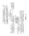
- FIG. 1is a block diagram of a data processing system according to one embodiment of the present invention.
- FIG. 2is a block diagram of one embodiment of a portion of a processor according to one embodiment of the present invention.
- FIG. 3is a block diagram of a cache coherency manager according to one embodiment of the present invention.
- FIG. 4is a flow diagram according to one embodiment of the present invention.
- FIG. 5is a timing diagram according to one embodiment of the present invention.
- busis used to refer to a plurality of signals or conductors which may be used to transfer one or more various types of information, such as data, addresses, control, or status.
- the conductors as discussed hereinmay be illustrated or described in reference to being a single conductor, a plurality of conductors, unidirectional conductors, or bidirectional conductors. However, different embodiments may vary the implementation of the conductors. For example, separate unidirectional conductors may be used rather than bidirectional conductors and vice versa.
- plurality of conductorsmay be replaced with a single conductor that transfers multiple signals serially or in a time multiplexed manner. Likewise, single conductors carrying multiple signals may be separated out into various different conductors carrying subsets of these signals. Therefore, many options exist for transferring signals.
- FIG. 1illustrates, in block diagram form, a data processing system 10 according to one embodiment of the present invention.
- Data processing system 10includes devices that enable data transactions to be completed prior to performing a snoop lookup operation.
- Data processing system 10includes processor 14 , processor 16 , cache coherency manager 18 , system transaction arbiter 32 , system memory 20 , other master devices 22 , other slave devices 24 , and input/output I/O devices 26 .
- the devices shown in FIG. 1are communicatively coupled to a system interconnect bus 12 but maybe coupled by other types of system interconnects in other embodiments.
- a system interconnectthat includes a cross bar switch or other type of switch, or a system interconnect that includes multiple busses and/or switches.
- a system interconnect busmay include multiple signal lines for address, data, and control information.
- System transaction arbiter 32arbitrates among various masters of system 10 for transactions on a system interconnect bus 12 .
- I/O devices 26may be any number of I/O devices such as keyboard controllers and communications ports.
- Other slave devices 24may include memory devices such as a system cache (e.g. L2 cache). Both devices 24 and 26 may be accessible by transactions on system interconnect bus 12 that are generated by the master devices of the system (e.g. processor 14 , processor 16 , or other master devices 22 ).
- other master devices 22includes other types of processors (e.g. a digital signal processor) or a direct memory access (DMA) device which can generate transactions on system interconnect bus 12 .
- each master devicemay also include a cache (not shown).
- System 10includes a cache coherency manager 18 that snoops system interconnect bus 12 for transactions and initiates snoop requests for various caches of system 10 (e.g. cache 28 , cache 30 ) of system 10 to determine whether the caches include the data operand of the transaction. If a cache contains the data operand, then that cache will invalidate the data operand in response to the snoop request.
- cache coherency manager 18that snoops system interconnect bus 12 for transactions and initiates snoop requests for various caches of system 10 (e.g. cache 28 , cache 30 ) of system 10 to determine whether the caches include the data operand of the transaction. If a cache contains the data operand, then that cache will invalidate the data operand in response to the snoop request.
- a transactionis a write transaction by processor 16 to system memory 20 for writing data to a location in memory 20 .
- cache coherency manager 18would generate a snoop request to the other caches (e.g. cache 28 ) to search for data of the same memory address. If a cache has an entry corresponding to the same memory address, then the cache would invalidate that data since an updated version is being provided to memory 20 on system interconnect bus 12 .
- system 101includes a snoop control interface between the cache coherency manager 18 and each of the processors 14 and 16 for exchanging information regarding snooping operations.
- the snoop control interfaceincludes snoop request lines, snoop status lines, snoop acknowledge lines, and snoop error lines. These lines will be discussed below.
- cache coherency manager 18only includes snoop control interfaces with processors 14 and 16 .
- cache coherency manager 18may include a snoop control interface with other devices having a cache (e.g. master devices 22 , slave devices 24 , and other caches).
- processors 14 and 16may include additional caches.
- other types of data systemsmay include different configurations and/or have additional circuitry.
- other embodimentsmay not have all of the circuitry shown in FIG. 1 .
- some or all of the circuitry shown in FIG. 1may be implemented on one integrated circuit.
- system 10may be implemented with multiple integrated circuits.
- system 10may be implemented as part of an information system such as e.g. a computer, cell phone, PDA, electronic control circuitry of an automobile, or other type of system implementing a data processing system.
- an information systemsuch as e.g. a computer, cell phone, PDA, electronic control circuitry of an automobile, or other type of system implementing a data processing system.
- FIG. 2is a block diagram of a portion of processor 14 according to one embodiment of the present invention.
- processor 14includes cache 28 , processing circuitry 40 , an arbiter 42 , a bus interface unit (BIU) 48 , snoop control 54 , and snoop queue circuitry 44 .
- BIUbus interface unit
- Processing circuitry 40may include circuitry typically found in a processor such as e.g. an instruction pipe unit, execution units, an instruction fetch unit, control circuitry, general purpose registers, a load store unit, and a prefetch unit. Processors of other embodiments may include other types of circuitry.
- processing circuitry 40executes instructions that generate requests for data to be read from system memory 20 (or other slave or I/O devices) and for data to be written to system memory 20 (or other slave or I/O devices).
- processing circuitry 40will check cache 28 (via arbiter 42 ) to see if it has any data that corresponds to that system memory address. If not, a load store unit of processing circuitry 40 will generate via BIU 48 a transaction on system interconnect bus 12 to request data from memory 20 at that system address.
- system memory 20will provide the requested data on system interconnect bus 12 to processor 14 wherein BIU 48 receives the data and provides the data to processing circuitry 40 and to cache 28 in some embodiments.
- BIU 48receives the data and provides the data to processing circuitry 40 and to cache 28 in some embodiments.
- the transactionis complete.
- Write transactions to memory 20can be initiated by processor 14 where a write address and data are provided on interconnect bus 12 to be written to memory 20 at the address. Also, data may be written to or read from other slave devices 24 and I/O devices 26 of data processing system 10 in other embodiments.
- Cache 28may be an instruction cache, a data cache, or a combination of the two.
- dataherein in regards to a transaction may refer to the information stored in either an instruction cache or a data cache.
- Processor 14also includes circuitry for snoop request management.
- the snoop request circuitryoperates to keep the data in cache 28 coherent with other copies of the data stored in memory 20 and other caches of data processing system 10 .
- Snoop control 54receives snoop requests from cache coherency manager 18 via the snoop control interface.
- Processor 14includes snoop queue circuitry 44 including a snoop queue 46 for storing snoop requests received from the snoop control interface.
- the snoop request queue 46may be implemented as a FIFO.
- the FIFOmay be implemented as a circular buffer.
- Each entry in the snoop request queue 46has an address field and a status field that includes status information.
- the address fieldstores the address of the transaction for which a snoop request was generated.
- a first status bitis a valid (V) bit which indicates whether the entry in the snoop request queue 46 is valid.
- Vvalid
- Other types of status bitsmay be included in other embodiments.
- Each entryalso includes a snoop request ID field that stores the snoop request ID for the snoop request generated by the cache coherency manager.
- snoop control 54 and snoop queue circuitry 44operate to keep cache 28 coherent with other copies of the information in system 10 .
- Snoop control 54receives a snoop request from cache coherency manager 18 via the snoop control interface and provides the address of the snoop request, along with the request ID to be stored in queue 46 .
- the arbiter 42arbitrates access to the cache 28 between the processing circuitry 40 and snoop queue circuitry 44 in an efficient manner to minimize the time that processing circuitry 40 does not have access to cache 28 .
- the minimization of accesses to cache 28 by the snoop control circuitrymay be accomplished in one embodiment, by selectively merging or collapsing two or more snoop address lookups into a single snoop address lookup.
- snoop control 54When a snoop request is received by snoop control 54 , snoop control 54 routes the snoop address to the snoop queue circuitry 44 .
- Various embodiment of the function of snoop queue circuitry 44may be implemented.
- all received snoop addresses from the snoop control 54are stored in the snoop request queue 46 .
- arbiter 42provides the snoop queue circuitry 44 with access to the cache 28 , access addresses from the processing circuitry 40 are not permitted to cache 28 via the arbiter 42 .
- arbiter 42provides the snoop addresses from the snoop request queue 46 to the cache 28 for searching.
- the snoop addressesare removed from the snoop request queue 46 on a first-in, first-out (FIFO) basis.
- the snoop queue circuitry 44When a snoop address is present in the snoop request queue 46 , the snoop queue circuitry 44 signals arbiter 42 to request arbiter 42 to arbitrate for access to the cache 28 .
- cache 28has a single set of address tags and therefore must be either be dedicated to the processor for addressing or to the snoop queue circuitry for addressing.
- arbiter 42prevents access by the processing circuitry 40 to cache 28
- snoop addresses from circuitry 44are routed through the arbiter 42 to the cache 28 . Circuitry within the cache 28 compares the snoop address with all the addresses presently stored in the cache 28 .
- snoop control 54may signal arbiter 42 to arbitrate for access to cache 28 .
- snoop address compressionmay be performed by circuitry 44 to reduce the time that circuitry 44 has access to cache 28 .
- a comparison of the next two or more snoop addressesis performed by comparison logic (not shown). The number of snoop addresses that are compared concurrently is a choice of design.
- a same tag and index portion for two addressesindicates that both addresses are within a same line of memory.
- the snoop control interfaceincludes a snoop request signal interface, a snoop status signal interface, a snoop acknowledgement signal interface, and a snoop error signal interface.
- the snoop request signal interfaceincludes a request signal line for indicating that a request being made, a snoop command line indicating the type of bus transaction that generated the snoop, a snoop address line which is the address of the transaction being snooped, and a snoop request ID line, which is a number generated by the cache coherency manager identifying the snoop request.
- These signal linesmay be multi-bit (either in parallel or serial in some embodiments) or single bit in some embodiments.
- the snoop acknowledge signal interfaceis used to indicate to the cache coherency manager 18 that a snoop request has been processed by the cache.
- the snoop status interfaceprovides the result of the cache snoop (e.g. whether an entry for the data address was found in the cache or not or whether an error (parity bit) was found with the data of the entry).
- the snoop acknowledge interfaceincludes a snoop response line and a snoop request ID line indicating the ID number of the snoop request. These lines may be multi-bit as well.
- the snoop control interfaceincludes a snoop error signal line.
- the snoop error signal lineis used by the cache coherency manager 18 to indicate to a processor that a transaction generated by the processor resulted in an error from another cache when snooped. Examples of errors include whether another cache finds that the data associated with the snooped address had a parity error or an ECC error.
- system 10may include processors of other configurations and/or that perform transactions and snoop operations in a different manner.
- a processormay have other circuitry not shown in FIG. 2 or may not include all of the circuitry shown in FIG. 2 .
- a processormay include other circuitry for handling snoop requests in another manner as well.
- FIG. 3is block diagram of one embodiment of cache coherency manager 18 .
- Manager 18is communicatively coupled to interconnect bus 12 to monitor the bus for write and read transactions that may require snooping of other caches in data processing system 10 .
- manager 18receives the address of the transaction from address lines, receives the master ID that generated a transaction from master ID lines, and receives a transaction type of the transaction from transaction type lines. In other embodiments, manager 18 may receive other types of data from interconnect bus 12 .
- Manager 18includes control logic 76 for controlling and performing operations of manager 18 .
- snoop requests to the caches of system 10are generated only in response to certain types of transactions on interconnect bus 12 . For example, in some embodiments, only write transactions generate snoop requests.
- Manager 18also includes an ID generator 72 for generating a request ID for each snoop request. Because data processing system 10 can complete transactions prior to the generation of the snoops for that transaction, manager 18 has the ability to generate IDs to distinguish a snoop request caused by one transaction from a snoop request generated by another transaction.
- each IDincludes a first number of bits indicating the Master ID and a second number of bits indicating a sequential number for each snoop request generated by a transaction of the master.
- the sequential numberis generated by counter 74 .
- Counter 74may includes a different count for each master of system 10 . In other embodiments, the count is incremented for each transaction that generates a snoop request regardless of the master initiating the transaction.
- Manager 18also includes a buffer 78 for storing outstanding snoop requests.
- snoop requestsare retired when snoop status signals are received from all caches to which a snoop request was sent.
- FIG. 4includes flow diagram showing one embodiment of the operation of data processing system in performing cache coherency operations.
- processor A(processor 14 , 16 , or another master device 22 ) initiates a transaction 1 to a desired target on system interconnect bus 12 .
- cache coherency manager 18determines whether memory coherency of transaction 1 is required for all other caches (or some caches) of data processing system 10 . In one embodiment, the determination of whether coherency is required is based on the transaction type, the master generating the transaction, or the desired target (e.g. a write to memory 20 ).
- the cache coherency manager 18If coherency is required (operation 84 ), then in operation 88 , the cache coherency manager 18 generates a snoop request to the other caches of data processing system 10 . For example, if processor 16 generated the transaction, manager 18 would send a snoop request via the snoop control interface to cache 28 . This snoop request would be received by snoop control 54 of processor 14 . A snoop request is not sent to cache 30 , in one embodiment, since processor 16 generated the snoop request.
- the cachesprocess the snoop request by checking their locations for an address matching the memory address of transaction 1 .
- the cachesprovide the results of the processing of their snoop request to manager 18 via the snoop acknowledge interface and snoop status interface. If there was a snoop error reported by any of the caches via the snoop status interface, then in operation 96 , manager 18 reports that error to processor A via the snoop error interface.
- transaction 1is completed by the target device in operation 98 .
- the system interconnect bus 12is ready to receive another transaction, wherein cache coherency manager 18 monitors the system interconnect bus 12 for another transaction in operation 100 .
- a data processing systemmay perform cache coherency operations by other methods.
- each cacheincludes a cache queue circuitry 44 that allows for multiple snoop requests to be stored.
- cache manager 18includes an ID generator 72 and request buffer that allow for multiple snoop requests to be outstanding at any one time.
- the system 10By completing the transaction prior to the processing of the snoop requests, the system 10 allows for a more efficient use of a system interconnect and allows for more transactions to be completed.
- FIG. 5is a timing diagram illustrating how a transaction can be completed before the results of a snoop request are returned.
- Signal 150is the initiation of a transaction A (the providing the address of transaction A on a system interconnect) by the master of transaction A.
- Signal 151is a snoop request being providing by the cache coherency manager 18 on a snoop control interface.
- Signal 152is the data of transaction A being provided on system interconnect bus 12 to the target device by the master of transaction A.
- Signal 154is the snoop acknowledgement provided by the cache to manager 18 on the snoop control interconnect.
- transaction Ais completed (as shown by the end of signal 152 ) before the results of the snoop requests are returned as indicated in signal 154 .
- Signal 156is the initiation of a transaction B (the providing the address of transaction B on a system interconnect) by master A to a target device.
- Signal 160is a snoop request being providing by the cache coherency manager 18 on a snoop control interface.
- Signal 158is the data provided on system interconnect bus 12 by the master of transaction B to be written to a target device.
- Signal 162is the snoop acknowledgement by the cache provided to manager 18 on the snoop control interface.
- transaction Bis completed (as indicated by the completion of signal 158 prior to the generation of the snoop request (signal 160 ) for that transaction.
- signal 166is the initiation of transaction C (the providing the address of transaction C on the system interconnect) by master A to a target device. Signal 166 occurs before a snoop request (signal 160 ) is sent by manager 18 for transaction B. Although a data signal for C is not shown in FIG. 5 , transaction C may be completed prior to generating the snoop request for transaction B (signal 160 ). In the embodiment shown, all transactions are generated by Master A. However, in other embodiments, transactions A, B, and C maybe generated by different masters. in some embodiments, a transaction is completed by an acknowledgement signal from the target device to the master.
- a data processing systemincludes a system interconnect and a first master communicatively coupled to initiate a transaction on the system interconnect.
- the transactionhas a corresponding access address.
- the systemincludes a second master and a cache coherency manager communicatively coupled to the system interconnect.
- the second masterincludes a cache and snoop circuitry which receives snoop requests from the cache coherency manager. A snoop lookup in the cache is performed for received snoop requests, and, in response to each snoop lookup, a snoop response is provided to the cache coherency manager.
- the snoop circuitryis configured to be capable of performing a snoop lookup operation for the snoop request corresponding to the transaction initiated by the first master after completion of the transaction initiated by the first master on the system interconnect.
- a second transaction subsequent to the transactioncan be initiated on the system interconnect prior to the completion of the snoop lookup.
- a methodin another embodiment, in a data processing system, includes a first master initiating a transaction via a system interconnect to a target device. The method also includes after the first master initiating, providing a snoop request corresponding to the transaction to a cache of a second master. The method further includes completing the transaction and after the completing, performing a snoop lookup operation corresponding to the snoop request in the cache of the second master.
- a methodin another embodiment, in a data processing system, includes a first master initiating a transaction via a system interconnect to a target device and after the first master initiating, a cache coherency manager providing a snoop request corresponding to the transaction to a cache of the data processing system. The method also includes completing the transaction and performing a snoop lookup operation corresponding to the snoop request in the cache. The method further includes in response to the performing the snoop lookup operation, providing a snoop response to the cache coherency manager. The providing the snoop response is performed after the completing the transaction.
Landscapes
- Engineering & Computer Science (AREA)
- Theoretical Computer Science (AREA)
- Physics & Mathematics (AREA)
- General Engineering & Computer Science (AREA)
- General Physics & Mathematics (AREA)
- Memory System Of A Hierarchy Structure (AREA)
Abstract
Description
Claims (22)
Priority Applications (1)
| Application Number | Priority Date | Filing Date | Title |
|---|---|---|---|
| US12/112,796US8706974B2 (en) | 2008-04-30 | 2008-04-30 | Snoop request management in a data processing system |
Applications Claiming Priority (1)
| Application Number | Priority Date | Filing Date | Title |
|---|---|---|---|
| US12/112,796US8706974B2 (en) | 2008-04-30 | 2008-04-30 | Snoop request management in a data processing system |
Publications (2)
| Publication Number | Publication Date |
|---|---|
| US20090276580A1 US20090276580A1 (en) | 2009-11-05 |
| US8706974B2true US8706974B2 (en) | 2014-04-22 |
Family
ID=41257884
Family Applications (1)
| Application Number | Title | Priority Date | Filing Date |
|---|---|---|---|
| US12/112,796Active2032-05-11US8706974B2 (en) | 2008-04-30 | 2008-04-30 | Snoop request management in a data processing system |
Country Status (1)
| Country | Link |
|---|---|
| US (1) | US8706974B2 (en) |
Cited By (2)
| Publication number | Priority date | Publication date | Assignee | Title |
|---|---|---|---|---|
| US9311244B2 (en)* | 2014-08-25 | 2016-04-12 | Arm Limited | Enforcing ordering of snoop transactions in an interconnect for an integrated circuit |
| US12026109B2 (en) | 2020-12-16 | 2024-07-02 | Samsung Electronics Co., Ltd. | Operating method of transaction accelerator, operating method of computing device including transaction accelerator, and computing device including transaction accelerator |
Families Citing this family (2)
| Publication number | Priority date | Publication date | Assignee | Title |
|---|---|---|---|---|
| US7757027B2 (en)* | 2008-06-19 | 2010-07-13 | Arm Limited | Control of master/slave communication within an integrated circuit |
| US12332783B2 (en)* | 2022-10-10 | 2025-06-17 | International Business Machines Corporation | Input/output (I/O) store protocol for pipelining coherent operations |
Citations (20)
| Publication number | Priority date | Publication date | Assignee | Title |
|---|---|---|---|---|
| US5506971A (en)* | 1992-03-04 | 1996-04-09 | Motorola, Inc. | Method and apparatus for performing a snoop-retry protocol in a data processing system |
| US5522057A (en) | 1993-10-25 | 1996-05-28 | Intel Corporation | Hybrid write back/write through cache having a streamlined four state cache coherency protocol for uniprocessor computer systems |
| US5699548A (en) | 1995-06-01 | 1997-12-16 | Intel Corporation | Method and apparatus for selecting a mode for updating external memory |
| US5761725A (en) | 1994-01-31 | 1998-06-02 | Dell Usa, L.P. | Cache-based computer system employing a peripheral bus interface unit with cache write-back suppression and processor-peripheral communication suppression for data coherency |
| US5860114A (en) | 1995-05-10 | 1999-01-12 | Cagent Technologies, Inc. | Method and apparatus for managing snoop requests using snoop advisory cells |
| US5920892A (en) | 1996-08-26 | 1999-07-06 | Unisys Corporation | Method and system for inhibiting transfer of duplicate write addresses in multi-domain processor systems with cross-bus architecture to reduce cross-invalidation requests |
| US6021468A (en) | 1997-04-14 | 2000-02-01 | International Business Machines Corporation | Cache coherency protocol with efficient write-through aliasing |
| US6292906B1 (en)* | 1997-12-17 | 2001-09-18 | Intel Corporation | Method and apparatus for detecting and compensating for certain snoop errors in a system with multiple agents having cache memories |
| US20030005236A1 (en) | 2001-06-29 | 2003-01-02 | International Business Machines Corporation | Imprecise snooping based invalidation mechanism |
| US6601144B1 (en) | 2000-10-26 | 2003-07-29 | International Business Machines Corporation | Dynamic cache management in a symmetric multiprocessor system via snoop operation sequence analysis |
| US20030195939A1 (en) | 2002-04-16 | 2003-10-16 | Edirisooriya Samatha J. | Conditional read and invalidate for use in coherent multiprocessor systems |
| US20040123046A1 (en) | 2002-12-19 | 2004-06-24 | Hum Herbert H.J. | Forward state for use in cache coherency in a multiprocessor system |
| US6845432B2 (en)* | 2000-12-28 | 2005-01-18 | Intel Corporation | Low power cache architecture |
| US20050071573A1 (en) | 2003-09-30 | 2005-03-31 | International Business Machines Corp. | Modified-invalid cache state to reduce cache-to-cache data transfer operations for speculatively-issued full cache line writes |
| US20050251628A1 (en) | 2004-05-10 | 2005-11-10 | Jarvis Thomas C | Method, system, and program for demoting tracks from cache |
| US20050251626A1 (en) | 2003-04-24 | 2005-11-10 | Newisys, Inc. | Managing sparse directory evictions in multiprocessor systems via memory locking |
| US7234029B2 (en) | 2000-12-28 | 2007-06-19 | Intel Corporation | Method and apparatus for reducing memory latency in a cache coherent multi-node architecture |
| US20080091884A1 (en) | 2006-10-17 | 2008-04-17 | Arm Limited | Handling of write access requests to shared memory in a data processing apparatus |
| US7373462B2 (en)* | 2005-03-29 | 2008-05-13 | International Business Machines Corporation | Snoop filter for filtering snoop requests |
| US20080183972A1 (en)* | 2007-01-26 | 2008-07-31 | James Norris Dieffenderfer | Snoop Filtering Using a Snoop Request Cache |
- 2008
- 2008-04-30USUS12/112,796patent/US8706974B2/enactiveActive
Patent Citations (20)
| Publication number | Priority date | Publication date | Assignee | Title |
|---|---|---|---|---|
| US5506971A (en)* | 1992-03-04 | 1996-04-09 | Motorola, Inc. | Method and apparatus for performing a snoop-retry protocol in a data processing system |
| US5522057A (en) | 1993-10-25 | 1996-05-28 | Intel Corporation | Hybrid write back/write through cache having a streamlined four state cache coherency protocol for uniprocessor computer systems |
| US5761725A (en) | 1994-01-31 | 1998-06-02 | Dell Usa, L.P. | Cache-based computer system employing a peripheral bus interface unit with cache write-back suppression and processor-peripheral communication suppression for data coherency |
| US5860114A (en) | 1995-05-10 | 1999-01-12 | Cagent Technologies, Inc. | Method and apparatus for managing snoop requests using snoop advisory cells |
| US5699548A (en) | 1995-06-01 | 1997-12-16 | Intel Corporation | Method and apparatus for selecting a mode for updating external memory |
| US5920892A (en) | 1996-08-26 | 1999-07-06 | Unisys Corporation | Method and system for inhibiting transfer of duplicate write addresses in multi-domain processor systems with cross-bus architecture to reduce cross-invalidation requests |
| US6021468A (en) | 1997-04-14 | 2000-02-01 | International Business Machines Corporation | Cache coherency protocol with efficient write-through aliasing |
| US6292906B1 (en)* | 1997-12-17 | 2001-09-18 | Intel Corporation | Method and apparatus for detecting and compensating for certain snoop errors in a system with multiple agents having cache memories |
| US6601144B1 (en) | 2000-10-26 | 2003-07-29 | International Business Machines Corporation | Dynamic cache management in a symmetric multiprocessor system via snoop operation sequence analysis |
| US6845432B2 (en)* | 2000-12-28 | 2005-01-18 | Intel Corporation | Low power cache architecture |
| US7234029B2 (en) | 2000-12-28 | 2007-06-19 | Intel Corporation | Method and apparatus for reducing memory latency in a cache coherent multi-node architecture |
| US20030005236A1 (en) | 2001-06-29 | 2003-01-02 | International Business Machines Corporation | Imprecise snooping based invalidation mechanism |
| US20030195939A1 (en) | 2002-04-16 | 2003-10-16 | Edirisooriya Samatha J. | Conditional read and invalidate for use in coherent multiprocessor systems |
| US20040123046A1 (en) | 2002-12-19 | 2004-06-24 | Hum Herbert H.J. | Forward state for use in cache coherency in a multiprocessor system |
| US20050251626A1 (en) | 2003-04-24 | 2005-11-10 | Newisys, Inc. | Managing sparse directory evictions in multiprocessor systems via memory locking |
| US20050071573A1 (en) | 2003-09-30 | 2005-03-31 | International Business Machines Corp. | Modified-invalid cache state to reduce cache-to-cache data transfer operations for speculatively-issued full cache line writes |
| US20050251628A1 (en) | 2004-05-10 | 2005-11-10 | Jarvis Thomas C | Method, system, and program for demoting tracks from cache |
| US7373462B2 (en)* | 2005-03-29 | 2008-05-13 | International Business Machines Corporation | Snoop filter for filtering snoop requests |
| US20080091884A1 (en) | 2006-10-17 | 2008-04-17 | Arm Limited | Handling of write access requests to shared memory in a data processing apparatus |
| US20080183972A1 (en)* | 2007-01-26 | 2008-07-31 | James Norris Dieffenderfer | Snoop Filtering Using a Snoop Request Cache |
Non-Patent Citations (17)
| Title |
|---|
| Final Office Action mailed Jul. 7, 2011 in U.S. Appl. No. 12/112,502. |
| Final Office Action mailed Jul. 7, 2011 in U.S. Appl. No. 12/112,508. |
| Office Action mailed Feb. 12, 2014 in U.S. Appl. No. 12/112,502. |
| Office Action mailed Feb. 18, 2011 in U.S. Appl. No. 12/112,508. |
| Office Action mailed Jun. 8, 2012 in U.S. Appl. No. 12/112,508. |
| Office Action mailed May 27, 2011 in U.S. Appl. No. 12/112,502. |
| Office Action mailed Nov. 19, 2013 in U.S. Appl. No. 12/112,502. |
| Office Action mailed Nov. 28, 2011 in U.S. Appl. No. 12/112,502. |
| Office Action Rejection mailed Feb. 22, 2013 in U.S. Appl. No. 12/112,502. |
| PCT Application No. PCT/US2009/034866 in related U.S. Appl. No. 11/112,502; Search Report and Written Opinion mailed Sep. 30, 2009. |
| U.S. Appl. No. 11/969,112, filed Jan. 3, 2008. |
| U.S. Appl. No. 12/053,761, filed Mar. 24, 2008. |
| U.S. Appl. No. 12/112,502, filed Apr. 30, 2008. |
| U.S. Appl. No. 12/112,502, Inventor Willaim C. Moyer, "Cache Coherency Protocol in a Data Processing System1", filed Apr. 30, 2008, Office Action-Rejection, mailed Aug. 16, 2012. |
| U.S. Appl. No. 12/112,502, Inventor William C. Moyer, filed Apr. 30, 2008, Office Action mailed Aug. 16, 2012. |
| U.S. Appl. No. 12/112,508, filed Apr. 30, 2008. |
| U.S. Appl. No. 12/112,508, Inventor William C. Moyer, "Cache Coherency Protocol in a Data Processing System", filed Apr. 20, 2008, Office Action-Notice of Allowance, mailed Dec. 7, 2012. |
Cited By (2)
| Publication number | Priority date | Publication date | Assignee | Title |
|---|---|---|---|---|
| US9311244B2 (en)* | 2014-08-25 | 2016-04-12 | Arm Limited | Enforcing ordering of snoop transactions in an interconnect for an integrated circuit |
| US12026109B2 (en) | 2020-12-16 | 2024-07-02 | Samsung Electronics Co., Ltd. | Operating method of transaction accelerator, operating method of computing device including transaction accelerator, and computing device including transaction accelerator |
Also Published As
| Publication number | Publication date |
|---|---|
| US20090276580A1 (en) | 2009-11-05 |
Similar Documents
| Publication | Publication Date | Title |
|---|---|---|
| CN113853593B (en) | Victim cache supporting flushing of write miss entries | |
| US8918591B2 (en) | Data processing system having selective invalidation of snoop requests and method therefor | |
| US7941584B2 (en) | Data processing apparatus and method for performing hazard detection | |
| JP5120850B2 (en) | Method, apparatus and computer program for filtering snoop requests using stream registers | |
| US6496902B1 (en) | Vector and scalar data cache for a vector multiprocessor | |
| KR100274771B1 (en) | Method of shared intervention for cache lines in the shared state for smp bus | |
| US6981106B1 (en) | System and method for accelerating ownership within a directory-based memory system | |
| US7447844B2 (en) | Data processing system, processor and method of data processing in which local memory access requests are serviced on a fixed schedule | |
| JP2008535093A5 (en) | ||
| US8291259B2 (en) | Delete of cache line with correctable error | |
| US20130151790A1 (en) | Efficient Storage of Meta-Bits Within a System Memory | |
| JPH10289156A (en) | Method and system for sharing and intervening cache line in latest reading state of smp bus | |
| JPH10289154A (en) | Method and device for sharing cache line in exclusive state of smp bus | |
| US7120836B1 (en) | System and method for increasing cache hit detection performance | |
| JP3007870B2 (en) | Method and apparatus for managing architectural operations | |
| US8706974B2 (en) | Snoop request management in a data processing system | |
| US7464227B2 (en) | Method and apparatus for supporting opportunistic sharing in coherent multiprocessors | |
| US20070061519A1 (en) | Early return indication for read exclusive requests in shared memory architecture | |
| US7581042B2 (en) | I/O hub resident cache line monitor and device register update | |
| US8131947B2 (en) | Cache snoop limiting within a multiple master data processing system | |
| JP3007871B2 (en) | Method and apparatus for managing architectural operations | |
| US8099560B2 (en) | Synchronization mechanism for use with a snoop queue | |
| JP2001043133A (en) | Method and system for maintaining cache coherency for write-through-store operation in multiprocessor system | |
| US9558119B2 (en) | Main memory operations in a symmetric multiprocessing computer | |
| US6898675B1 (en) | Data received before coherency window for a snoopy bus |
Legal Events
| Date | Code | Title | Description |
|---|---|---|---|
| AS | Assignment | Owner name:CITIBANK, N.A., NEW YORK Free format text:SECURITY AGREEMENT;ASSIGNOR:FREESCALE SEMICONDUCTOR, INC.;REEL/FRAME:021570/0449 Effective date:20080728 Owner name:CITIBANK, N.A.,NEW YORK Free format text:SECURITY AGREEMENT;ASSIGNOR:FREESCALE SEMICONDUCTOR, INC.;REEL/FRAME:021570/0449 Effective date:20080728 | |
| AS | Assignment | Owner name:CITIBANK, N.A., NEW YORK Free format text:SECURITY AGREEMENT;ASSIGNOR:FREESCALE SEMICONDUCTOR, INC.;REEL/FRAME:024085/0001 Effective date:20100219 Owner name:CITIBANK, N.A.,NEW YORK Free format text:SECURITY AGREEMENT;ASSIGNOR:FREESCALE SEMICONDUCTOR, INC.;REEL/FRAME:024085/0001 Effective date:20100219 | |
| AS | Assignment | Owner name:CITIBANK, N.A., AS COLLATERAL AGENT, NEW YORK Free format text:SECURITY AGREEMENT;ASSIGNOR:FREESCALE SEMICONDUCTOR, INC.;REEL/FRAME:024397/0001 Effective date:20100413 Owner name:CITIBANK, N.A., AS COLLATERAL AGENT,NEW YORK Free format text:SECURITY AGREEMENT;ASSIGNOR:FREESCALE SEMICONDUCTOR, INC.;REEL/FRAME:024397/0001 Effective date:20100413 | |
| AS | Assignment | Owner name:CITIBANK, N.A., AS NOTES COLLATERAL AGENT, NEW YORK Free format text:SECURITY AGREEMENT;ASSIGNOR:FREESCALE SEMICONDUCTOR, INC.;REEL/FRAME:030633/0424 Effective date:20130521 Owner name:CITIBANK, N.A., AS NOTES COLLATERAL AGENT, NEW YOR Free format text:SECURITY AGREEMENT;ASSIGNOR:FREESCALE SEMICONDUCTOR, INC.;REEL/FRAME:030633/0424 Effective date:20130521 | |
| AS | Assignment | Owner name:CITIBANK, N.A., AS NOTES COLLATERAL AGENT, NEW YORK Free format text:SECURITY AGREEMENT;ASSIGNOR:FREESCALE SEMICONDUCTOR, INC.;REEL/FRAME:031591/0266 Effective date:20131101 Owner name:CITIBANK, N.A., AS NOTES COLLATERAL AGENT, NEW YOR Free format text:SECURITY AGREEMENT;ASSIGNOR:FREESCALE SEMICONDUCTOR, INC.;REEL/FRAME:031591/0266 Effective date:20131101 | |
| STCF | Information on status: patent grant | Free format text:PATENTED CASE | |
| AS | Assignment | Owner name:FREESCALE SEMICONDUCTOR, INC., TEXAS Free format text:PATENT RELEASE;ASSIGNOR:CITIBANK, N.A., AS COLLATERAL AGENT;REEL/FRAME:037356/0143 Effective date:20151207 Owner name:FREESCALE SEMICONDUCTOR, INC., TEXAS Free format text:PATENT RELEASE;ASSIGNOR:CITIBANK, N.A., AS COLLATERAL AGENT;REEL/FRAME:037354/0719 Effective date:20151207 Owner name:FREESCALE SEMICONDUCTOR, INC., TEXAS Free format text:PATENT RELEASE;ASSIGNOR:CITIBANK, N.A., AS COLLATERAL AGENT;REEL/FRAME:037356/0553 Effective date:20151207 | |
| AS | Assignment | Owner name:MORGAN STANLEY SENIOR FUNDING, INC., MARYLAND Free format text:ASSIGNMENT AND ASSUMPTION OF SECURITY INTEREST IN PATENTS;ASSIGNOR:CITIBANK, N.A.;REEL/FRAME:037486/0517 Effective date:20151207 | |
| AS | Assignment | Owner name:MORGAN STANLEY SENIOR FUNDING, INC., MARYLAND Free format text:ASSIGNMENT AND ASSUMPTION OF SECURITY INTEREST IN PATENTS;ASSIGNOR:CITIBANK, N.A.;REEL/FRAME:037518/0292 Effective date:20151207 | |
| AS | Assignment | Owner name:MORGAN STANLEY SENIOR FUNDING, INC., MARYLAND Free format text:SUPPLEMENT TO THE SECURITY AGREEMENT;ASSIGNOR:FREESCALE SEMICONDUCTOR, INC.;REEL/FRAME:039138/0001 Effective date:20160525 | |
| AS | Assignment | Owner name:NXP, B.V., F/K/A FREESCALE SEMICONDUCTOR, INC., NETHERLANDS Free format text:RELEASE BY SECURED PARTY;ASSIGNOR:MORGAN STANLEY SENIOR FUNDING, INC.;REEL/FRAME:040925/0001 Effective date:20160912 Owner name:NXP, B.V., F/K/A FREESCALE SEMICONDUCTOR, INC., NE Free format text:RELEASE BY SECURED PARTY;ASSIGNOR:MORGAN STANLEY SENIOR FUNDING, INC.;REEL/FRAME:040925/0001 Effective date:20160912 | |
| AS | Assignment | Owner name:NXP B.V., NETHERLANDS Free format text:RELEASE BY SECURED PARTY;ASSIGNOR:MORGAN STANLEY SENIOR FUNDING, INC.;REEL/FRAME:040928/0001 Effective date:20160622 | |
| AS | Assignment | Owner name:NXP USA, INC., TEXAS Free format text:CHANGE OF NAME;ASSIGNOR:FREESCALE SEMICONDUCTOR, INC.;REEL/FRAME:040632/0001 Effective date:20161107 | |
| AS | Assignment | Owner name:MORGAN STANLEY SENIOR FUNDING, INC., MARYLAND Free format text:CORRECTIVE ASSIGNMENT TO CORRECT THE REMOVE PATENTS 8108266 AND 8062324 AND REPLACE THEM WITH 6108266 AND 8060324 PREVIOUSLY RECORDED ON REEL 037518 FRAME 0292. ASSIGNOR(S) HEREBY CONFIRMS THE ASSIGNMENT AND ASSUMPTION OF SECURITY INTEREST IN PATENTS;ASSIGNOR:CITIBANK, N.A.;REEL/FRAME:041703/0536 Effective date:20151207 | |
| MAFP | Maintenance fee payment | Free format text:PAYMENT OF MAINTENANCE FEE, 4TH YEAR, LARGE ENTITY (ORIGINAL EVENT CODE: M1551) Year of fee payment:4 | |
| AS | Assignment | Owner name:NXP USA, INC., TEXAS Free format text:CORRECTIVE ASSIGNMENT TO CORRECT THE NATURE OF CONVEYANCE PREVIOUSLY RECORDED AT REEL: 040632 FRAME: 0001. ASSIGNOR(S) HEREBY CONFIRMS THE MERGER AND CHANGE OF NAME;ASSIGNOR:FREESCALE SEMICONDUCTOR INC.;REEL/FRAME:044209/0047 Effective date:20161107 | |
| AS | Assignment | Owner name:SHENZHEN XINGUODU TECHNOLOGY CO., LTD., CHINA Free format text:CORRECTIVE ASSIGNMENT TO CORRECT THE TO CORRECT THE APPLICATION NO. FROM 13,883,290 TO 13,833,290 PREVIOUSLY RECORDED ON REEL 041703 FRAME 0536. ASSIGNOR(S) HEREBY CONFIRMS THE THE ASSIGNMENT AND ASSUMPTION OF SECURITYINTEREST IN PATENTS.;ASSIGNOR:MORGAN STANLEY SENIOR FUNDING, INC.;REEL/FRAME:048734/0001 Effective date:20190217 | |
| AS | Assignment | Owner name:NXP B.V., NETHERLANDS Free format text:RELEASE BY SECURED PARTY;ASSIGNOR:MORGAN STANLEY SENIOR FUNDING, INC.;REEL/FRAME:050744/0097 Effective date:20190903 | |
| AS | Assignment | Owner name:MORGAN STANLEY SENIOR FUNDING, INC., MARYLAND Free format text:CORRECTIVE ASSIGNMENT TO CORRECT THE REMOVE APPLICATION11759915 AND REPLACE IT WITH APPLICATION 11759935 PREVIOUSLY RECORDED ON REEL 037486 FRAME 0517. ASSIGNOR(S) HEREBY CONFIRMS THE ASSIGNMENT AND ASSUMPTION OF SECURITYINTEREST IN PATENTS;ASSIGNOR:CITIBANK, N.A.;REEL/FRAME:053547/0421 Effective date:20151207 | |
| AS | Assignment | Owner name:NXP B.V., NETHERLANDS Free format text:CORRECTIVE ASSIGNMENT TO CORRECT THE REMOVEAPPLICATION 11759915 AND REPLACE IT WITH APPLICATION11759935 PREVIOUSLY RECORDED ON REEL 040928 FRAME 0001. ASSIGNOR(S) HEREBY CONFIRMS THE RELEASE OF SECURITYINTEREST;ASSIGNOR:MORGAN STANLEY SENIOR FUNDING, INC.;REEL/FRAME:052915/0001 Effective date:20160622 | |
| AS | Assignment | Owner name:NXP, B.V. F/K/A FREESCALE SEMICONDUCTOR, INC., NETHERLANDS Free format text:CORRECTIVE ASSIGNMENT TO CORRECT THE REMOVEAPPLICATION 11759915 AND REPLACE IT WITH APPLICATION11759935 PREVIOUSLY RECORDED ON REEL 040925 FRAME 0001. ASSIGNOR(S) HEREBY CONFIRMS THE RELEASE OF SECURITYINTEREST;ASSIGNOR:MORGAN STANLEY SENIOR FUNDING, INC.;REEL/FRAME:052917/0001 Effective date:20160912 | |
| MAFP | Maintenance fee payment | Free format text:PAYMENT OF MAINTENANCE FEE, 8TH YEAR, LARGE ENTITY (ORIGINAL EVENT CODE: M1552); ENTITY STATUS OF PATENT OWNER: LARGE ENTITY Year of fee payment:8 | |
| MAFP | Maintenance fee payment | Free format text:PAYMENT OF MAINTENANCE FEE, 12TH YEAR, LARGE ENTITY (ORIGINAL EVENT CODE: M1553); ENTITY STATUS OF PATENT OWNER: LARGE ENTITY Year of fee payment:12 |