US8704450B2 - Flash LED controller - Google Patents
Flash LED controllerDownload PDFInfo
- Publication number
- US8704450B2 US8704450B2US13/037,353US201113037353AUS8704450B2US 8704450 B2US8704450 B2US 8704450B2US 201113037353 AUS201113037353 AUS 201113037353AUS 8704450 B2US8704450 B2US 8704450B2
- Authority
- US
- United States
- Prior art keywords
- current
- capacitors
- super
- load
- source
- Prior art date
- Legal status (The legal status is an assumption and is not a legal conclusion. Google has not performed a legal analysis and makes no representation as to the accuracy of the status listed.)
- Expired - Fee Related, expires
Links
- 239000003990capacitorSubstances0.000abstractdescription53
- 238000000034methodMethods0.000abstractdescription16
- 230000002459sustained effectEffects0.000description7
- 238000013459approachMethods0.000description6
- 230000008901benefitEffects0.000description5
- 238000010586diagramMethods0.000description5
- 230000001105regulatory effectEffects0.000description5
- 238000013461designMethods0.000description4
- 238000001514detection methodMethods0.000description3
- 238000012544monitoring processMethods0.000description3
- HBBGRARXTFLTSG-UHFFFAOYSA-NLithium ionChemical compound[Li+]HBBGRARXTFLTSG-UHFFFAOYSA-N0.000description2
- 229910001416lithium ionInorganic materials0.000description2
- 230000003466anti-cipated effectEffects0.000description1
- 239000003985ceramic capacitorSubstances0.000description1
- 230000001276controlling effectEffects0.000description1
- 230000001419dependent effectEffects0.000description1
- 238000011161developmentMethods0.000description1
- 230000018109developmental processEffects0.000description1
- 230000003292diminished effectEffects0.000description1
- 238000004146energy storageMethods0.000description1
- 230000001667episodic effectEffects0.000description1
- 230000002431foraging effectEffects0.000description1
- 230000006872improvementEffects0.000description1
- 230000007774longtermEffects0.000description1
- 239000000463materialSubstances0.000description1
- 238000005259measurementMethods0.000description1
- 230000007246mechanismEffects0.000description1
- 238000004377microelectronicMethods0.000description1
- 238000012986modificationMethods0.000description1
- 230000004048modificationEffects0.000description1
- 230000000153supplemental effectEffects0.000description1
- 230000001360synchronised effectEffects0.000description1
- 230000007704transitionEffects0.000description1
- 229910052724xenonInorganic materials0.000description1
- FHNFHKCVQCLJFQ-UHFFFAOYSA-Nxenon atomChemical compound[Xe]FHNFHKCVQCLJFQ-UHFFFAOYSA-N0.000description1
Images


Classifications
- H—ELECTRICITY
- H05—ELECTRIC TECHNIQUES NOT OTHERWISE PROVIDED FOR
- H05B—ELECTRIC HEATING; ELECTRIC LIGHT SOURCES NOT OTHERWISE PROVIDED FOR; CIRCUIT ARRANGEMENTS FOR ELECTRIC LIGHT SOURCES, IN GENERAL
- H05B45/00—Circuit arrangements for operating light-emitting diodes [LED]
- H05B45/40—Details of LED load circuits
- H05B45/44—Details of LED load circuits with an active control inside an LED matrix
- H05B45/46—Details of LED load circuits with an active control inside an LED matrix having LEDs disposed in parallel lines
- H—ELECTRICITY
- H05—ELECTRIC TECHNIQUES NOT OTHERWISE PROVIDED FOR
- H05B—ELECTRIC HEATING; ELECTRIC LIGHT SOURCES NOT OTHERWISE PROVIDED FOR; CIRCUIT ARRANGEMENTS FOR ELECTRIC LIGHT SOURCES, IN GENERAL
- H05B45/00—Circuit arrangements for operating light-emitting diodes [LED]
- H05B45/30—Driver circuits
- H05B45/37—Converter circuits
- H05B45/3725—Switched mode power supply [SMPS]
- H05B45/38—Switched mode power supply [SMPS] using boost topology
Definitions
- the inventionrelates to electronics and microelectronic circuitry.
- the inventionis directed to integrated power supplies, circuit drivers, and control methods.
- Li-Ion batteriesoften used in such applications are limited in their voltage capacities, however, and are often incapable of withstanding the high currents required for driving the LEDs.
- the inventionprovides advances in the arts with novel methods and apparatus directed to useful for power supplies, converters, and drivers.
- a preferred embodiment of a circuitincludes at least one high series resistance super-capacitor coupled for driving a load.
- the super-capacitors(s)are electrically connected with a power supply for charging.
- a low resistance driver circuitis connected for regulating power supplied from the super-capacitors to the load based on output current detection.
- a circuitin a presently preferred embodiment, includes high series resistance super-capacitors charged by a battery power source.
- the super-capacitorsare coupled for driving a load consisting of one or more LEDs.
- the voltage requirements of the LEDsare such that driving them directly with the battery power source would be impractical.
- a low resistance driver circuitis connected for regulating power supplied from the super-capacitors to the load based on load current.
- the above-described circuitsmay be implemented using parallel and/or series combinations of super-capacitors, driver circuits, and load components.
- high series resistance super-capacitorsare coupled for driving a load.
- a low resistance driver circuit connected for regulating power from the super-capacitors to the loadincludes a PWM switch control.
- preferred embodimentsencompass methods for using high series resistance super-capacitors to drive loads including steps for charging the super-capacitors and subsequently regulating their output to the load by using feedback sensed at the load.
- preferred methods of the inventioninclude steps for dynamically compensating for ambient conditions, load component mismatch, or other variations in output requirements.
- the inventionhas advantages including but not limited to one or more of the following, energy efficiency, area efficiency, and cost-effectiveness in providing high drive currents in systems using relatively low voltage batteries.
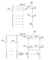
- FIG. 1is a simplified schematic circuit diagram illustrating an example of preferred embodiments of circuits, systems, and methods according to the invention
- FIG. 2is a simplified schematic circuit diagram illustrating an example of alternative preferred embodiments of circuits, systems, and methods according to the invention using PWM for regulating output;
- FIG. 3is a simplified schematic circuit diagram illustrating an example of alternative preferred embodiments of circuits, systems, and methods according to the invention implemented using a combination of super-capacitors;
- FIG. 4is a simplified schematic circuit diagram illustrating an example of alternative preferred embodiments of circuits, systems, and methods according to the invention implemented with a combination of load components;
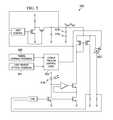
- FIG. 5is a simplified schematic circuit diagram illustrating an example of alternative preferred embodiments of circuits, systems, and methods according to the invention.
- a fully-integrated power supply and multi-channel driver for LED applicationsis configured to charge super-capacitors using a DC/DC synchronous switching boost regulator with fully integrated power switches, internal compensation, and full fault protection.
- a very low resistance driveris used to energize the driven load, in this example LEDs, with minimal loss of super-capacitor rail voltage headroom.
- the charging of the super-capacitorsis preferably accomplished operating in a regulation mode by providing current feedback to the boost regulator.
- the circuitrydraws very little quiescent current and periodically refreshes the charge on the super-capacitors as needed.
- a circuit 10is shown in which a battery 12 is coupled to a boost regulator 14 for charging two super-capacitors 16 .
- the super-capacitors 16are coupled in series with a load device, in this example an LED 18 , having fairly high voltage and current requirements relative to the battery 12 .
- the super-capacitors 16are selected for their ability to provide a relatively high current pulse at the LED 18 without overtaxing the battery 12 .
- Suitable super-capacitorsgenerally have a maximum working voltage within the range of approximately 2.5-2.7V.
- any number of super-capacitorsmay be placed in series, but on the other hand, it is desirable to minimize the number of large capacitors that must be used in a system. It is characteristic for suitable super-capacitors to have a high Equivalent Series Resistance (ESR). In order to make the most of available voltage from the high-ESR super-capacitors, it is preferred to drive the LED from the capacitors using a low-resistance switching mechanism.
- ESREquivalent Series Resistance
- the ratio of peak to average currentcan be held to approximately 1.5:1 or 2:1, which is advantageous in terms of long-term reliability and, in LED systems, for consistency in color temperature.
- the approach for ensuring sufficient drive current availability while using high ESR super-capacitorsis to directly drive the load with very low resistance switch FETs 20 .
- the boost voltageis preferably set to be just sufficient to drive the load to maximum current assuming the upper limit of the load's forward voltage. When load component mismatch, temperature, or other conditions are such that the forward voltage is less than this upper limit, the driver automatically responds accordingly, driving the FETs at a level which results in the desired average current.
- the current level in each channelis preferably controlled individually.
- PWMpulse width modulate
- the switchso that the average current through the load is set to a desired value independent of the variation in peak current caused by variations in the forward voltage drop of the load. It is desirable to choose a switching frequency which is above the audible band, but still low enough to favor system efficiency and effective regulation of the average load current during an operating cycle.
- the period under loadis on the order of approximately 30-50 ms.
- the period of a 20 kHz PWM frequencybeing 50 ⁇ S
- a pulse count of roughly 1000can easily be achieved for one flash cycle. This has been found to be ample to ensure accurate regulation of the flash current.
- FIG. 2depicts an example of a preferred embodiment of a circuit implementation of a current-controlled PWM LED driver circuit 200 .
- the battery 212is coupled to a boost regulator 214 for charging two super-capacitors 216 in the manner described previously. Coupled in series with a load 218 , the super-capacitors 216 drive the load 218 under the control of a low-voltage, current-controlled PWM switch 220 .
- the monitored DC output level 224is used to determine the suitable duty cycle to drive the load 218 , in this example, a bank of two or more LEDs placed in parallel.
- the inventionmay be practiced in implementing a flash mode, for powering episodic high-intensity events such as a camera flash, and a sustained mode for longer term operation such as for a portable projector or lighting application.
- a system switchable between the two modesit may be preferable to provide a system switchable between the two modes.
- the operational modeis preferably monitored by a watch dog timer for protection.
- the timercan be switched between a flash mode and a sustained mode.
- a maximum value selected for a flash mode eventmay correspond to a maximum duration of 1 second, and 1280 seconds ( ⁇ 21 minutes) for a sustained mode event.
- a small section of the large power FET used for flash driveis used to drive the LEDs in sustained mode.
- the power FETis operated as a linear current sink, which is preferably user-programmable, the mode being selected by a user via a serial interface.
- compensationis preferably optimized for using a combination of high-ESR super capacitors and low-ESR ceramic capacitors to supply the large short-term current demands of the load elements and their associated drivers.
- itincludes flexibility to be used for a wide range of output voltages, corresponding to a wide range of forward voltages.
- the regulatoris configured to automatically transition between pulse frequency modulation (PFM) and PWM modes to maximize efficiency based on the load demand.
- PFM architectureincludes power saving circuitry to minimize battery drain, even when the boost regulator is enabled full time.
- circuitryis configured for very low current PFM hysteretic power saving features.
- the regulatorWhen the regulator detects very light load conditions, it operates in a low duty cycle condition limited by minimum duty cycle detection in the regulator. This can cause the output voltage to reach an overvoltage condition although this voltage level is very close to the normal output voltage level with less than 3% difference and typically around 1 to 2% higher than the normal operational voltage. When this level of output voltage is detected, a low power mode is entered whereby the device is turned off for power savings.
- the regulatorhowever maintains the voltage on the output capacitors(s) by monitoring the output voltage and turning on when an undervoltage is detected. This undervoltage level is also typically less than 3% below normal operating voltage and typically 1 to 2% below the normal operational voltage. Upon detection of the undervoltage level, the circuit is turned on to charge the output capacitor(s).
- the regulatoroperates in a low power mode to conserve power hysteritically.
- This low power modesustains the charge on the output super-capacitor(s) while conserving power for the large majority of the time when the super-capacitor is charged.
- a larger number of super-capacitors 316may be placed in series and/or parallel combinations in order to apply the same methods.
- This configuration 300is shown in FIG. 3 .
- multiple driver combinationsmay be used in parallel, wherein multiple loads 418 may be driven from the same super-capacitor or combination of super-capacitors 416 , as illustrated in FIG. 4 .
- Differences in forward voltages among individual load componentsmay require different duty cycles for each, resulting in sudden differences in supply voltage, for example, in the event one LED in a load of multiple LEDs is turned off before its neighbor.
- a sense resistormay be used in series with the driver transistor in order to accurately measure the current at that point.
- the resistor valueis preferably kept very small, since there is only one large current value required.
- An improvement in system efficiencymay also be realized in some applications by implementing direct drain current sensing of the driver transistor. Again, since there is only one large value of average load current required, this can be achieved using IC design techniques known to those skilled in the arts if an integrated driver transistor is employed.
- a separate supplemental DC current source 502 or sinkmay also be used to drive the LED 518 without excessive power dissipation.
- thismay be implemented using a linear regulator in combination with a smaller drive transistor to minimize switching loss.
- Additional monitoring and control featuresmay also be included with the embodiments shown and described, such as a sensor 520 suitable for monitoring ambient temperature or light conditions and adjusting the load current accordingly, and using a look-up table for aging values of LEDs so that the current can be compensated as the system ages.
Landscapes
- Circuit Arrangement For Electric Light Sources In General (AREA)
- Led Devices (AREA)
- Dc-Dc Converters (AREA)
Abstract
Description
Claims (3)
Priority Applications (1)
| Application Number | Priority Date | Filing Date | Title |
|---|---|---|---|
| US13/037,353US8704450B2 (en) | 2010-02-26 | 2011-02-28 | Flash LED controller |
Applications Claiming Priority (2)
| Application Number | Priority Date | Filing Date | Title |
|---|---|---|---|
| US30883010P | 2010-02-26 | 2010-02-26 | |
| US13/037,353US8704450B2 (en) | 2010-02-26 | 2011-02-28 | Flash LED controller |
Publications (2)
| Publication Number | Publication Date |
|---|---|
| US20120104962A1 US20120104962A1 (en) | 2012-05-03 |
| US8704450B2true US8704450B2 (en) | 2014-04-22 |
Family
ID=45995950
Family Applications (1)
| Application Number | Title | Priority Date | Filing Date |
|---|---|---|---|
| US13/037,353Expired - Fee RelatedUS8704450B2 (en) | 2010-02-26 | 2011-02-28 | Flash LED controller |
Country Status (1)
| Country | Link |
|---|---|
| US (1) | US8704450B2 (en) |
Cited By (15)
| Publication number | Priority date | Publication date | Assignee | Title |
|---|---|---|---|---|
| US9599660B2 (en) | 2009-02-23 | 2017-03-21 | Triune Ip, Llc | Electrical interconnect status monitoring system |
| US9843314B2 (en) | 2011-07-10 | 2017-12-12 | Triune Systems, LLC | Pop and click noise reduction |
| US9853441B2 (en) | 2011-07-10 | 2017-12-26 | Triune Systems, LLC | Voltage transient protection circuitry |
| US9955429B2 (en) | 2015-11-24 | 2018-04-24 | Microsoft Technology Licensing, Llc | Battery current consumption adjustment for an illumination unit |
| US10079090B2 (en) | 2010-12-01 | 2018-09-18 | Triune Systems, LLC | Multiple coil data transmission system |
| US10186897B2 (en) | 2012-02-21 | 2019-01-22 | Triune Ip Llc | Scalable harvesting system and method |
| US10250081B2 (en) | 2012-01-17 | 2019-04-02 | Triune Systems, LLC | Method and system of wireless power transfer foreign object detection |
| USRE47441E1 (en) | 2008-07-21 | 2019-06-18 | Triune Ip Llc | Monitoring method, circuit and system |
| US10348131B2 (en) | 2010-12-01 | 2019-07-09 | Triune Systems, LLC | Couple inductor power transfer system |
| US10396590B2 (en) | 2011-03-22 | 2019-08-27 | Triune Systems, LLC | Variable power energy harvesting system |
| US10574297B2 (en) | 2009-11-25 | 2020-02-25 | Triune Ip, Llc | Multi-use wireless power and data system |
| USRE47900E1 (en) | 2008-07-21 | 2020-03-10 | Triune Ip, Llc | Memory for programming a floating gate using an analog comparison device coupled to a tunneling device |
| US10673489B2 (en) | 2014-03-04 | 2020-06-02 | Triune Ip Llc | Isolation for communication and power |
| US10854378B2 (en) | 2009-02-23 | 2020-12-01 | Triune Ip Llc | Wireless power transmittal |
| US11622428B1 (en)* | 2022-05-19 | 2023-04-04 | Pixart Imaging Inc. | Constant current LED driver, current control circuit and programmable current source |
Families Citing this family (11)
| Publication number | Priority date | Publication date | Assignee | Title |
|---|---|---|---|---|
| JP6087960B2 (en)* | 2012-03-09 | 2017-03-01 | フィリップス ライティング ホールディング ビー ヴィ | LED light source |
| KR101360685B1 (en)* | 2012-05-31 | 2014-02-10 | 엘지이노텍 주식회사 | Illumination system reduced standby power |
| US9001265B2 (en) | 2013-02-12 | 2015-04-07 | Non-Typical, Inc. | Illumination assembly for a scouting camera |
| US9585211B2 (en)* | 2013-09-17 | 2017-02-28 | Skyworks Solutions, Inc. | Flash-LED driver discharge control |
| US9648217B2 (en)* | 2015-03-21 | 2017-05-09 | Erik A. Kaiser | Selfie apparatus |
| US9801242B2 (en) | 2015-09-29 | 2017-10-24 | Skyworks Soluteqns, Enc. | Apparatus and methods for boost regulators with dynamic regulation band |
| US11436858B2 (en) | 2017-07-09 | 2022-09-06 | Ringo Ai, Inc. | Characterizing reflectance, illuminance, and sensor response for electromagnetic radiation |
| WO2019014147A2 (en) | 2017-07-09 | 2019-01-17 | Lumenetix, Inc. | TECHNIQUES FOR CREATING CHARACTERIZATION MATRICES FOR REFLECTANCE, LIGHTING OR SENSOR RESPONSE |
| US11263428B2 (en) | 2017-07-09 | 2022-03-01 | Ringo Ai, Inc. | Electromagnetic emitters and detectors for electronic devices |
| CN110505729B (en)* | 2018-05-18 | 2021-11-30 | 华润微集成电路(无锡)有限公司 | Modulation circuit for improving LED dimming depth and modulation method thereof |
| US11956551B2 (en)* | 2022-05-31 | 2024-04-09 | Microsoft Technology Licensing, Llc | Systems and methods for camera exposure controlled strobing lights |
Citations (7)
| Publication number | Priority date | Publication date | Assignee | Title |
|---|---|---|---|---|
| US6538394B2 (en)* | 2001-03-30 | 2003-03-25 | Maxim Integrated Products, Inc. | Current source methods and apparatus for light emitting diodes |
| US7250810B1 (en)* | 2005-12-27 | 2007-07-31 | Aimtron Technology Corp. | Multi-mode charge pump drive circuit with improved input noise at a moment of mode change |
| US20090108775A1 (en)* | 2007-10-30 | 2009-04-30 | Texas Instruments Deutschland Gmbh | Led driver with adaptive algorithm for storage capacitor pre-charge |
| US20090121653A1 (en)* | 2005-01-20 | 2009-05-14 | Taisuke Chida | Constant Current Circuit, Light Emitting Apparatus and Power Supply Apparatus Using That Constant Current Circuit |
| US20100327928A1 (en)* | 2009-06-26 | 2010-12-30 | Texas Instruments Incorporated | Method and apparatus to improve and control the propagation delay in a current slewing circuit |
| US7991282B1 (en)* | 2008-12-08 | 2011-08-02 | National Semiconductor Corporation | Method and circuit for charging of super capacitor as energy source for flash diodes |
| US8077139B2 (en)* | 2009-04-16 | 2011-12-13 | Chunghwa Picture Tubes, Ltd. | Driving circuit of backlight module |
- 2011
- 2011-02-28USUS13/037,353patent/US8704450B2/ennot_activeExpired - Fee Related
Patent Citations (7)
| Publication number | Priority date | Publication date | Assignee | Title |
|---|---|---|---|---|
| US6538394B2 (en)* | 2001-03-30 | 2003-03-25 | Maxim Integrated Products, Inc. | Current source methods and apparatus for light emitting diodes |
| US20090121653A1 (en)* | 2005-01-20 | 2009-05-14 | Taisuke Chida | Constant Current Circuit, Light Emitting Apparatus and Power Supply Apparatus Using That Constant Current Circuit |
| US7250810B1 (en)* | 2005-12-27 | 2007-07-31 | Aimtron Technology Corp. | Multi-mode charge pump drive circuit with improved input noise at a moment of mode change |
| US20090108775A1 (en)* | 2007-10-30 | 2009-04-30 | Texas Instruments Deutschland Gmbh | Led driver with adaptive algorithm for storage capacitor pre-charge |
| US7991282B1 (en)* | 2008-12-08 | 2011-08-02 | National Semiconductor Corporation | Method and circuit for charging of super capacitor as energy source for flash diodes |
| US8077139B2 (en)* | 2009-04-16 | 2011-12-13 | Chunghwa Picture Tubes, Ltd. | Driving circuit of backlight module |
| US20100327928A1 (en)* | 2009-06-26 | 2010-12-30 | Texas Instruments Incorporated | Method and apparatus to improve and control the propagation delay in a current slewing circuit |
Cited By (18)
| Publication number | Priority date | Publication date | Assignee | Title |
|---|---|---|---|---|
| USRE47441E1 (en) | 2008-07-21 | 2019-06-18 | Triune Ip Llc | Monitoring method, circuit and system |
| USRE47900E1 (en) | 2008-07-21 | 2020-03-10 | Triune Ip, Llc | Memory for programming a floating gate using an analog comparison device coupled to a tunneling device |
| US11309126B2 (en) | 2009-02-23 | 2022-04-19 | Triune Systems, LLC | Wireless power transmittal |
| US10854378B2 (en) | 2009-02-23 | 2020-12-01 | Triune Ip Llc | Wireless power transmittal |
| US9599660B2 (en) | 2009-02-23 | 2017-03-21 | Triune Ip, Llc | Electrical interconnect status monitoring system |
| US11368191B2 (en) | 2009-11-25 | 2022-06-21 | Triune Ip, Llc | Multi-use wireless power and data system |
| US10574297B2 (en) | 2009-11-25 | 2020-02-25 | Triune Ip, Llc | Multi-use wireless power and data system |
| US10348131B2 (en) | 2010-12-01 | 2019-07-09 | Triune Systems, LLC | Couple inductor power transfer system |
| US10079090B2 (en) | 2010-12-01 | 2018-09-18 | Triune Systems, LLC | Multiple coil data transmission system |
| US11159053B2 (en) | 2010-12-01 | 2021-10-26 | Triune Systems, LLC | Coupled inductor power transfer system |
| US10396590B2 (en) | 2011-03-22 | 2019-08-27 | Triune Systems, LLC | Variable power energy harvesting system |
| US9853441B2 (en) | 2011-07-10 | 2017-12-26 | Triune Systems, LLC | Voltage transient protection circuitry |
| US9843314B2 (en) | 2011-07-10 | 2017-12-12 | Triune Systems, LLC | Pop and click noise reduction |
| US10250081B2 (en) | 2012-01-17 | 2019-04-02 | Triune Systems, LLC | Method and system of wireless power transfer foreign object detection |
| US10186897B2 (en) | 2012-02-21 | 2019-01-22 | Triune Ip Llc | Scalable harvesting system and method |
| US10673489B2 (en) | 2014-03-04 | 2020-06-02 | Triune Ip Llc | Isolation for communication and power |
| US9955429B2 (en) | 2015-11-24 | 2018-04-24 | Microsoft Technology Licensing, Llc | Battery current consumption adjustment for an illumination unit |
| US11622428B1 (en)* | 2022-05-19 | 2023-04-04 | Pixart Imaging Inc. | Constant current LED driver, current control circuit and programmable current source |
Also Published As
| Publication number | Publication date |
|---|---|
| US20120104962A1 (en) | 2012-05-03 |
Similar Documents
| Publication | Publication Date | Title |
|---|---|---|
| US8704450B2 (en) | Flash LED controller | |
| US6873322B2 (en) | Adaptive LCD power supply circuit | |
| KR101191701B1 (en) | Integrated device providing current-regulated charge pump driver with capacitor-propotional current | |
| US8148919B2 (en) | Circuits and methods for driving light sources | |
| US9071139B2 (en) | High current switching converter for LED applications | |
| US8581514B2 (en) | Dimming circuit and method for LEDs | |
| KR20060120508A (en) | LED driving circuit | |
| US20120175956A1 (en) | Dc power supply feeding system | |
| US7489109B1 (en) | Integrated battery charger and system regulator circuit | |
| JP2017085725A (en) | Step-down dc/dc converter, control circuit thereof, and on-vehicle power supply device | |
| KR20060046370A (en) | Electronic device with boost circuit | |
| US20220173657A1 (en) | Control circuit for an electronic converter, related integrated circuit, electronic converter and method of operating an electronic converter | |
| EP2206228B1 (en) | Single inductor power supply system with extremely high psrr for dual supply active matrix oled displays | |
| JP2010154655A (en) | Power system | |
| US8531113B2 (en) | Driving apparatus and driving method of LED device | |
| US9942956B1 (en) | Boost converter design with 100%-pass mode for WLED backlight and camera flash applications | |
| US8183787B2 (en) | Power supply systems with controllable power | |
| JP4236602B2 (en) | Switching power supply circuit and electronic device using the same | |
| CN117997112A (en) | Power supply circuit and switching power supply using same | |
| JP2009118589A (en) | DC booster circuit and guide lamp device | |
| CN112020182B (en) | Load control device, load control method, and non-transitory recording medium | |
| JP2023546958A (en) | Driver circuit for GaN switch mode power converter | |
| CN107885154A (en) | Programmable logic controller (PLC) | |
| KR101730629B1 (en) | Power converting apparatus and method of sensing output current thereof | |
| JP4609285B2 (en) | Semiconductor integrated circuit for power supply and power supply device |
Legal Events
| Date | Code | Title | Description |
|---|---|---|---|
| AS | Assignment | Owner name:TRIUNE IP LLC, TEXAS Free format text:ASSIGNMENT OF ASSIGNORS INTEREST;ASSIGNORS:CHEN, WAYNE;KNIGHT, JONATHAN;TEGGATZ, ROSS;AND OTHERS;SIGNING DATES FROM 20110225 TO 20110516;REEL/FRAME:026283/0523 | |
| STCF | Information on status: patent grant | Free format text:PATENTED CASE | |
| AS | Assignment | Owner name:HSBC BANK USA, NATIONAL ASSOCIATION, CALIFORNIA Free format text:SECURITY INTEREST;ASSIGNOR:TRIUNE IP, LLC;REEL/FRAME:035732/0326 Effective date:20150513 | |
| FEPP | Fee payment procedure | Free format text:PAT HOLDER NO LONGER CLAIMS SMALL ENTITY STATUS, ENTITY STATUS SET TO UNDISCOUNTED (ORIGINAL EVENT CODE: STOL); ENTITY STATUS OF PATENT OWNER: LARGE ENTITY | |
| RF | Reissue application filed | Effective date:20160218 | |
| AS | Assignment | Owner name:HSBC BANK USA, NATIONAL ASSOCIATION, AS ADMINISTRATIVE AGENT, CALIFORNIA Free format text:SECURITY INTEREST;ASSIGNORS:SEMTECH CORPORATION;SEMTECH NEW YORK CORPORATION;SIERRA MONOLITHICS, INC.;AND OTHERS;SIGNING DATES FROM 20151115 TO 20161115;REEL/FRAME:040646/0799 Owner name:HSBC BANK USA, NATIONAL ASSOCIATION, AS ADMINISTRA Free format text:SECURITY INTEREST;ASSIGNORS:SEMTECH CORPORATION;SEMTECH NEW YORK CORPORATION;SIERRA MONOLITHICS, INC.;AND OTHERS;SIGNING DATES FROM 20151115 TO 20161115;REEL/FRAME:040646/0799 | |
| MAFP | Maintenance fee payment | Free format text:PAYMENT OF MAINTENANCE FEE, 4TH YEAR, LARGE ENTITY (ORIGINAL EVENT CODE: M1551) Year of fee payment:4 | |
| FEPP | Fee payment procedure | Free format text:MAINTENANCE FEE REMINDER MAILED (ORIGINAL EVENT CODE: REM.); ENTITY STATUS OF PATENT OWNER: LARGE ENTITY | |
| LAPS | Lapse for failure to pay maintenance fees | Free format text:PATENT EXPIRED FOR FAILURE TO PAY MAINTENANCE FEES (ORIGINAL EVENT CODE: EXP.); ENTITY STATUS OF PATENT OWNER: LARGE ENTITY | |
| STCH | Information on status: patent discontinuation | Free format text:PATENT EXPIRED DUE TO NONPAYMENT OF MAINTENANCE FEES UNDER 37 CFR 1.362 | |
| FP | Lapsed due to failure to pay maintenance fee | Effective date:20220422 | |
| AS | Assignment | Owner name:JPMORGAN CHASE BANK, N.A., AS SUCCESSOR AGENT, ILLINOIS Free format text:ASSIGNMENT OF PATENT SECURITY INTEREST PREVIOUSLY RECORDED AT REEL/FRAME (040646/0799);ASSIGNOR:HSBC BANK USA, NATIONAL ASSOCIATION, AS RESIGNING AGENT;REEL/FRAME:062781/0544 Effective date:20230210 |