US8704360B1 - Top port surface mount silicon condenser microphone package - Google Patents
Top port surface mount silicon condenser microphone packageDownload PDFInfo
- Publication number
- US8704360B1 US8704360B1US13/732,179US201213732179AUS8704360B1US 8704360 B1US8704360 B1US 8704360B1US 201213732179 AUS201213732179 AUS 201213732179AUS 8704360 B1US8704360 B1US 8704360B1
- Authority
- US
- United States
- Prior art keywords
- mems microphone
- circuit board
- printed circuit
- substrate
- metal pads
- Prior art date
- Legal status (The legal status is an assumption and is not a legal conclusion. Google has not performed a legal analysis and makes no representation as to the accuracy of the status listed.)
- Expired - Fee Related
Links
Images


Classifications
- H—ELECTRICITY
- H04—ELECTRIC COMMUNICATION TECHNIQUE
- H04R—LOUDSPEAKERS, MICROPHONES, GRAMOPHONE PICK-UPS OR LIKE ACOUSTIC ELECTROMECHANICAL TRANSDUCERS; DEAF-AID SETS; PUBLIC ADDRESS SYSTEMS
- H04R1/00—Details of transducers, loudspeakers or microphones
- H04R1/20—Arrangements for obtaining desired frequency or directional characteristics
- H04R1/22—Arrangements for obtaining desired frequency or directional characteristics for obtaining desired frequency characteristic only
- H04R1/28—Transducer mountings or enclosures modified by provision of mechanical or acoustic impedances, e.g. resonator, damping means
- H04R1/2869—Reduction of undesired resonances, i.e. standing waves within enclosure, or of undesired vibrations, i.e. of the enclosure itself
- H04R1/2892—Mountings or supports for transducers
- B—PERFORMING OPERATIONS; TRANSPORTING
- B81—MICROSTRUCTURAL TECHNOLOGY
- B81B—MICROSTRUCTURAL DEVICES OR SYSTEMS, e.g. MICROMECHANICAL DEVICES
- B81B3/00—Devices comprising flexible or deformable elements, e.g. comprising elastic tongues or membranes
- B81B3/0018—Structures acting upon the moving or flexible element for transforming energy into mechanical movement or vice versa, i.e. actuators, sensors, generators
- B81B3/0021—Transducers for transforming electrical into mechanical energy or vice versa
- B—PERFORMING OPERATIONS; TRANSPORTING
- B81—MICROSTRUCTURAL TECHNOLOGY
- B81B—MICROSTRUCTURAL DEVICES OR SYSTEMS, e.g. MICROMECHANICAL DEVICES
- B81B7/00—Microstructural systems; Auxiliary parts of microstructural devices or systems
- B81B7/0032—Packages or encapsulation
- B81B7/0035—Packages or encapsulation for maintaining a controlled atmosphere inside of the chamber containing the MEMS
- B81B7/0038—Packages or encapsulation for maintaining a controlled atmosphere inside of the chamber containing the MEMS using materials for controlling the level of pressure, contaminants or moisture inside of the package, e.g. getters
- B—PERFORMING OPERATIONS; TRANSPORTING
- B81—MICROSTRUCTURAL TECHNOLOGY
- B81B—MICROSTRUCTURAL DEVICES OR SYSTEMS, e.g. MICROMECHANICAL DEVICES
- B81B7/00—Microstructural systems; Auxiliary parts of microstructural devices or systems
- B81B7/0032—Packages or encapsulation
- B81B7/0058—Packages or encapsulation for protecting against damages due to external chemical or mechanical influences, e.g. shocks or vibrations
- B—PERFORMING OPERATIONS; TRANSPORTING
- B81—MICROSTRUCTURAL TECHNOLOGY
- B81B—MICROSTRUCTURAL DEVICES OR SYSTEMS, e.g. MICROMECHANICAL DEVICES
- B81B7/00—Microstructural systems; Auxiliary parts of microstructural devices or systems
- B81B7/0032—Packages or encapsulation
- B81B7/0061—Packages or encapsulation suitable for fluid transfer from the MEMS out of the package or vice versa, e.g. transfer of liquid, gas, sound
- B—PERFORMING OPERATIONS; TRANSPORTING
- B81—MICROSTRUCTURAL TECHNOLOGY
- B81B—MICROSTRUCTURAL DEVICES OR SYSTEMS, e.g. MICROMECHANICAL DEVICES
- B81B7/00—Microstructural systems; Auxiliary parts of microstructural devices or systems
- B81B7/0032—Packages or encapsulation
- B81B7/0064—Packages or encapsulation for protecting against electromagnetic or electrostatic interferences
- B—PERFORMING OPERATIONS; TRANSPORTING
- B81—MICROSTRUCTURAL TECHNOLOGY
- B81B—MICROSTRUCTURAL DEVICES OR SYSTEMS, e.g. MICROMECHANICAL DEVICES
- B81B7/00—Microstructural systems; Auxiliary parts of microstructural devices or systems
- B81B7/0032—Packages or encapsulation
- B81B7/007—Interconnections between the MEMS and external electrical signals
- B—PERFORMING OPERATIONS; TRANSPORTING
- B81—MICROSTRUCTURAL TECHNOLOGY
- B81C—PROCESSES OR APPARATUS SPECIALLY ADAPTED FOR THE MANUFACTURE OR TREATMENT OF MICROSTRUCTURAL DEVICES OR SYSTEMS
- B81C1/00—Manufacture or treatment of devices or systems in or on a substrate
- B81C1/00015—Manufacture or treatment of devices or systems in or on a substrate for manufacturing microsystems
- B81C1/00134—Manufacture or treatment of devices or systems in or on a substrate for manufacturing microsystems comprising flexible or deformable structures
- B81C1/00158—Diaphragms, membranes
- B—PERFORMING OPERATIONS; TRANSPORTING
- B81—MICROSTRUCTURAL TECHNOLOGY
- B81C—PROCESSES OR APPARATUS SPECIALLY ADAPTED FOR THE MANUFACTURE OR TREATMENT OF MICROSTRUCTURAL DEVICES OR SYSTEMS
- B81C1/00—Manufacture or treatment of devices or systems in or on a substrate
- B81C1/00015—Manufacture or treatment of devices or systems in or on a substrate for manufacturing microsystems
- B81C1/00261—Processes for packaging MEMS devices
- B81C1/00301—Connecting electric signal lines from the MEMS device with external electrical signal lines, e.g. through vias
- B—PERFORMING OPERATIONS; TRANSPORTING
- B81—MICROSTRUCTURAL TECHNOLOGY
- B81C—PROCESSES OR APPARATUS SPECIALLY ADAPTED FOR THE MANUFACTURE OR TREATMENT OF MICROSTRUCTURAL DEVICES OR SYSTEMS
- B81C3/00—Assembling of devices or systems from individually processed components
- H—ELECTRICITY
- H01—ELECTRIC ELEMENTS
- H01L—SEMICONDUCTOR DEVICES NOT COVERED BY CLASS H10
- H01L21/00—Processes or apparatus adapted for the manufacture or treatment of semiconductor or solid state devices or of parts thereof
- H01L21/70—Manufacture or treatment of devices consisting of a plurality of solid state components formed in or on a common substrate or of parts thereof; Manufacture of integrated circuit devices or of parts thereof
- H01L21/77—Manufacture or treatment of devices consisting of a plurality of solid state components or integrated circuits formed in, or on, a common substrate
- H01L21/78—Manufacture or treatment of devices consisting of a plurality of solid state components or integrated circuits formed in, or on, a common substrate with subsequent division of the substrate into plural individual devices
- H—ELECTRICITY
- H01—ELECTRIC ELEMENTS
- H01L—SEMICONDUCTOR DEVICES NOT COVERED BY CLASS H10
- H01L23/00—Details of semiconductor or other solid state devices
- H01L23/02—Containers; Seals
- H01L23/10—Containers; Seals characterised by the material or arrangement of seals between parts, e.g. between cap and base of the container or between leads and walls of the container
- H—ELECTRICITY
- H01—ELECTRIC ELEMENTS
- H01L—SEMICONDUCTOR DEVICES NOT COVERED BY CLASS H10
- H01L23/00—Details of semiconductor or other solid state devices
- H01L23/12—Mountings, e.g. non-detachable insulating substrates
- H01L23/14—Mountings, e.g. non-detachable insulating substrates characterised by the material or its electrical properties
- H01L23/15—Ceramic or glass substrates
- H—ELECTRICITY
- H04—ELECTRIC COMMUNICATION TECHNIQUE
- H04R—LOUDSPEAKERS, MICROPHONES, GRAMOPHONE PICK-UPS OR LIKE ACOUSTIC ELECTROMECHANICAL TRANSDUCERS; DEAF-AID SETS; PUBLIC ADDRESS SYSTEMS
- H04R1/00—Details of transducers, loudspeakers or microphones
- H04R1/02—Casings; Cabinets ; Supports therefor; Mountings therein
- H04R1/04—Structural association of microphone with electric circuitry therefor
- H—ELECTRICITY
- H04—ELECTRIC COMMUNICATION TECHNIQUE
- H04R—LOUDSPEAKERS, MICROPHONES, GRAMOPHONE PICK-UPS OR LIKE ACOUSTIC ELECTROMECHANICAL TRANSDUCERS; DEAF-AID SETS; PUBLIC ADDRESS SYSTEMS
- H04R1/00—Details of transducers, loudspeakers or microphones
- H04R1/20—Arrangements for obtaining desired frequency or directional characteristics
- H04R1/22—Arrangements for obtaining desired frequency or directional characteristics for obtaining desired frequency characteristic only
- H04R1/222—Arrangements for obtaining desired frequency or directional characteristics for obtaining desired frequency characteristic only for microphones
- H—ELECTRICITY
- H04—ELECTRIC COMMUNICATION TECHNIQUE
- H04R—LOUDSPEAKERS, MICROPHONES, GRAMOPHONE PICK-UPS OR LIKE ACOUSTIC ELECTROMECHANICAL TRANSDUCERS; DEAF-AID SETS; PUBLIC ADDRESS SYSTEMS
- H04R19/00—Electrostatic transducers
- H04R19/005—Electrostatic transducers using semiconductor materials
- H—ELECTRICITY
- H04—ELECTRIC COMMUNICATION TECHNIQUE
- H04R—LOUDSPEAKERS, MICROPHONES, GRAMOPHONE PICK-UPS OR LIKE ACOUSTIC ELECTROMECHANICAL TRANSDUCERS; DEAF-AID SETS; PUBLIC ADDRESS SYSTEMS
- H04R19/00—Electrostatic transducers
- H04R19/01—Electrostatic transducers characterised by the use of electrets
- H04R19/016—Electrostatic transducers characterised by the use of electrets for microphones
- H—ELECTRICITY
- H04—ELECTRIC COMMUNICATION TECHNIQUE
- H04R—LOUDSPEAKERS, MICROPHONES, GRAMOPHONE PICK-UPS OR LIKE ACOUSTIC ELECTROMECHANICAL TRANSDUCERS; DEAF-AID SETS; PUBLIC ADDRESS SYSTEMS
- H04R19/00—Electrostatic transducers
- H04R19/04—Microphones
- H—ELECTRICITY
- H04—ELECTRIC COMMUNICATION TECHNIQUE
- H04R—LOUDSPEAKERS, MICROPHONES, GRAMOPHONE PICK-UPS OR LIKE ACOUSTIC ELECTROMECHANICAL TRANSDUCERS; DEAF-AID SETS; PUBLIC ADDRESS SYSTEMS
- H04R23/00—Transducers other than those covered by groups H04R9/00 - H04R21/00
- H—ELECTRICITY
- H04—ELECTRIC COMMUNICATION TECHNIQUE
- H04R—LOUDSPEAKERS, MICROPHONES, GRAMOPHONE PICK-UPS OR LIKE ACOUSTIC ELECTROMECHANICAL TRANSDUCERS; DEAF-AID SETS; PUBLIC ADDRESS SYSTEMS
- H04R3/00—Circuits for transducers, loudspeakers or microphones
- H—ELECTRICITY
- H04—ELECTRIC COMMUNICATION TECHNIQUE
- H04R—LOUDSPEAKERS, MICROPHONES, GRAMOPHONE PICK-UPS OR LIKE ACOUSTIC ELECTROMECHANICAL TRANSDUCERS; DEAF-AID SETS; PUBLIC ADDRESS SYSTEMS
- H04R31/00—Apparatus or processes specially adapted for the manufacture of transducers or diaphragms therefor
- H04R31/006—Interconnection of transducer parts
- B—PERFORMING OPERATIONS; TRANSPORTING
- B81—MICROSTRUCTURAL TECHNOLOGY
- B81B—MICROSTRUCTURAL DEVICES OR SYSTEMS, e.g. MICROMECHANICAL DEVICES
- B81B2201/00—Specific applications of microelectromechanical systems
- B81B2201/02—Sensors
- B81B2201/0257—Microphones or microspeakers
- B—PERFORMING OPERATIONS; TRANSPORTING
- B81—MICROSTRUCTURAL TECHNOLOGY
- B81B—MICROSTRUCTURAL DEVICES OR SYSTEMS, e.g. MICROMECHANICAL DEVICES
- B81B2207/00—Microstructural systems or auxiliary parts thereof
- B81B2207/09—Packages
- B81B2207/091—Arrangements for connecting external electrical signals to mechanical structures inside the package
- B81B2207/092—Buried interconnects in the substrate or in the lid
- H—ELECTRICITY
- H01—ELECTRIC ELEMENTS
- H01L—SEMICONDUCTOR DEVICES NOT COVERED BY CLASS H10
- H01L2924/00—Indexing scheme for arrangements or methods for connecting or disconnecting semiconductor or solid-state bodies as covered by H01L24/00
- H01L2924/0001—Technical content checked by a classifier
- H01L2924/0002—Not covered by any one of groups H01L24/00, H01L24/00 and H01L2224/00
- H—ELECTRICITY
- H01—ELECTRIC ELEMENTS
- H01L—SEMICONDUCTOR DEVICES NOT COVERED BY CLASS H10
- H01L2924/00—Indexing scheme for arrangements or methods for connecting or disconnecting semiconductor or solid-state bodies as covered by H01L24/00
- H01L2924/10—Details of semiconductor or other solid state devices to be connected
- H01L2924/146—Mixed devices
- H01L2924/1461—MEMS
- H—ELECTRICITY
- H04—ELECTRIC COMMUNICATION TECHNIQUE
- H04R—LOUDSPEAKERS, MICROPHONES, GRAMOPHONE PICK-UPS OR LIKE ACOUSTIC ELECTROMECHANICAL TRANSDUCERS; DEAF-AID SETS; PUBLIC ADDRESS SYSTEMS
- H04R2201/00—Details of transducers, loudspeakers or microphones covered by H04R1/00 but not provided for in any of its subgroups
- H04R2201/003—Mems transducers or their use
- H—ELECTRICITY
- H04—ELECTRIC COMMUNICATION TECHNIQUE
- H04R—LOUDSPEAKERS, MICROPHONES, GRAMOPHONE PICK-UPS OR LIKE ACOUSTIC ELECTROMECHANICAL TRANSDUCERS; DEAF-AID SETS; PUBLIC ADDRESS SYSTEMS
- H04R2225/00—Details of deaf aids covered by H04R25/00, not provided for in any of its subgroups
- H04R2225/49—Reducing the effects of electromagnetic noise on the functioning of hearing aids, by, e.g. shielding, signal processing adaptation, selective (de)activation of electronic parts in hearing aid
- H—ELECTRICITY
- H04—ELECTRIC COMMUNICATION TECHNIQUE
- H04R—LOUDSPEAKERS, MICROPHONES, GRAMOPHONE PICK-UPS OR LIKE ACOUSTIC ELECTROMECHANICAL TRANSDUCERS; DEAF-AID SETS; PUBLIC ADDRESS SYSTEMS
- H04R2410/00—Microphones
- H04R2410/03—Reduction of intrinsic noise in microphones
- Y—GENERAL TAGGING OF NEW TECHNOLOGICAL DEVELOPMENTS; GENERAL TAGGING OF CROSS-SECTIONAL TECHNOLOGIES SPANNING OVER SEVERAL SECTIONS OF THE IPC; TECHNICAL SUBJECTS COVERED BY FORMER USPC CROSS-REFERENCE ART COLLECTIONS [XRACs] AND DIGESTS
- Y10—TECHNICAL SUBJECTS COVERED BY FORMER USPC
- Y10T—TECHNICAL SUBJECTS COVERED BY FORMER US CLASSIFICATION
- Y10T29/00—Metal working
- Y10T29/49—Method of mechanical manufacture
- Y10T29/49002—Electrical device making
- Y10T29/49005—Acoustic transducer
- Y—GENERAL TAGGING OF NEW TECHNOLOGICAL DEVELOPMENTS; GENERAL TAGGING OF CROSS-SECTIONAL TECHNOLOGIES SPANNING OVER SEVERAL SECTIONS OF THE IPC; TECHNICAL SUBJECTS COVERED BY FORMER USPC CROSS-REFERENCE ART COLLECTIONS [XRACs] AND DIGESTS
- Y10—TECHNICAL SUBJECTS COVERED BY FORMER USPC
- Y10T—TECHNICAL SUBJECTS COVERED BY FORMER US CLASSIFICATION
- Y10T29/00—Metal working
- Y10T29/49—Method of mechanical manufacture
- Y10T29/49002—Electrical device making
- Y10T29/4902—Electromagnet, transformer or inductor
- Y10T29/4908—Acoustic transducer
- Y—GENERAL TAGGING OF NEW TECHNOLOGICAL DEVELOPMENTS; GENERAL TAGGING OF CROSS-SECTIONAL TECHNOLOGIES SPANNING OVER SEVERAL SECTIONS OF THE IPC; TECHNICAL SUBJECTS COVERED BY FORMER USPC CROSS-REFERENCE ART COLLECTIONS [XRACs] AND DIGESTS
- Y10—TECHNICAL SUBJECTS COVERED BY FORMER USPC
- Y10T—TECHNICAL SUBJECTS COVERED BY FORMER US CLASSIFICATION
- Y10T29/00—Metal working
- Y10T29/49—Method of mechanical manufacture
- Y10T29/49789—Obtaining plural product pieces from unitary workpiece
- Y10T29/49798—Dividing sequentially from leading end, e.g., by cutting or breaking
Definitions
- This patentrelates generally to a housing for a transducer. More particularly, this patent relates to a silicon condenser microphone including a housing for shielding a transducer.
- a silicon condenser microphoneincludes a transducer and a substrate and a cover forming the housing.
- the substratemay have an upper surface with a recess formed therein allowing the transducer to be attached to the upper surface and to overlap at least a portion of the recess thus forming a back volume.
- the coveris placed over the transducer and includes an aperture adapted for allowing sound waves to reach the transducer.
- FIG. 1is a cross-sectional view of a first embodiment of a silicon condenser microphone of the present invention
- FIG. 2is a cross-sectional view of a second embodiment of a silicon condenser microphone of the present invention
- FIG. 3is a cross-sectional view of a third embodiment of a silicon condenser microphone of the present invention.
- FIG. 4is a cross-sectional view of the third embodiment of the present invention affixed to an end user circuit board;
- FIG. 5is a cross-sectional view of the third embodiment of the present invention affixed to an end user circuit board in an alternate fashion;
- FIG. 6is a plan view of a substrate to which a silicon condenser microphone is fixed;
- FIG. 7is a longitudinal cross-sectional view of a microphone package of the present invention.
- FIG. 8is a lateral cross-sectional view of a microphone package of the present invention.
- FIG. 9is a longitudinal cross-sectional view of a microphone package of the present invention.
- FIG. 10is a lateral cross-sectional view of a microphone package of the present invention.
- FIG. 11is a cross-sectional view of a top portion for a microphone package of the present invention.
- FIG. 12is a cross-sectional view of a top portion for a microphone package of the present invention.
- FIG. 13is a cross-sectional view of a top portion for a microphone package of the present invention.
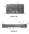
- FIG. 14 ais a cross-sectional view of a laminated bottom portion of a housing for a microphone package of the present invention
- FIG. 14 bis a plan view of a layer of the laminated bottom portion of FIG. 14 a;
- FIG. 14 cis a plan view of a layer of the laminated bottom portion of FIG. 14 a;
- FIG. 14 dis a plan view of a layer of the laminated bottom portion of FIG. 14 a;
- FIG. 15is a cross-sectional view of a bottom portion for a microphone package of the present invention.
- FIG. 16is a cross-sectional view of a bottom portion for a microphone package of the present invention.
- FIG. 17is a cross-sectional view of a bottom portion for a microphone package of the present invention.
- FIG. 18is a cross-sectional view of a bottom portion for a microphone package of the present invention.
- FIG. 19is a plan view of a side portion for a microphone package of the present invention.
- FIG. 20is a cross-sectional view of a side portion for a microphone package of the present invention.
- FIG. 21is a cross-sectional view of a side portion for a microphone package of the present invention.
- FIG. 22is a cross-sectional view of a side portion for a microphone package of the present invention.
- FIG. 23is a cross-sectional view of a microphone package of the present invention.
- FIG. 24is a cross-sectional view of a microphone package of the present invention.
- FIG. 25is a cross-sectional view of a microphone package of the present invention.
- FIG. 26is a cross-sectional view of a microphone package of the present invention.
- FIG. 27is a cross-sectional view of a microphone package of the present invention with a retaining ring
- FIG. 28is a cross-sectional view of a microphone package of the present invention with a retaining wing
- FIG. 29is a cross-sectional view of a microphone package of the present invention with a retaining ring
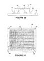
- FIG. 30is a plan view of a panel of a plurality of microphone packages.
- FIG. 31is a plan view of a microphone pair.
- the present inventionis directed to microphone packages.
- the benefits of the microphone packages disclosed herein over microphone packaging utilizing plastic body/lead framesinclude the ability to process packages in panel form allowing more units to be formed per operation and at much lower cost.
- the typical lead frame for a similarly functioning packagewould contain between 40 and 100 devices connected together.
- the present disclosurewould have approximately 14,000 devices connected together (as a panel).
- the embodiments disclosed hereinrequire minimal “hard-tooling” This allows the process to adjust to custom layout requirements without having to redesign mold, lead frame, and trim/form tooling.
- the described embodimentshave a better match of thermal coefficients of expansion with the end user's PCB, typically made of FR-4, since the microphone package is also made primarily of FR-4.
- These embodiments of the inventionmay also eliminate the need for wire bonding that is required in plastic body/lead frame packages.
- the footprintis typically smaller than that would be required for a plastic body/lead frame design since the leads may be formed by plating a through-hole in a circuit board to form the pathway to the solder pad.
- a (gull wing configurationwould be used in which the leads widen the overall foot print.
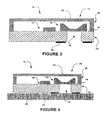
- FIGS. 1-3three embodiments of a silicon condenser microphone package 10 of the present invention are illustrated.
- a transducer 12e.g. a silicon condenser microphone as disclosed in U.S. Pat. No. 5,870,482 which is hereby incorporated by reference and an amplifier 16 .
- the packageitself includes a substrate 14 , a back volume or air cavity 18 , which provides a pressure reference for the transducer 12 , and a cover 20 .
- the substrate 14may be formed of FR-4 material allowing processing in circuit board panel form, thus taking advantage of economies of scale in manufacturing.
- FIG. 6is a plan view of the substrate 14 showing the back volume 18 surrounded a plurality of terminal pads.
- the back volume 18may be formed by a number of methods, including controlled depth drilling of an upper surface 19 of the substrate 14 to form a recess over which the transducer 12 is mounted ( FIG. 1 ); drilling and routing of several individual sheets of FR-4 and laminating the individual sheets to form the back volume 18 , which may or may not have internal support posts ( FIG. 2 ); or drilling completely through the substrate 14 and providing a sealing ring 22 on the bottom of the device that will seal the back volume 18 during surface mounting to a user's “board” 28 ( FIGS. 3-5 ).
- the combination of the substrate and the user's board 28creates the back volume 18 .
- the back volume 18is covered by the transducer 12 (e.g., a MEMS device) which may be “bumpbonded” and mounted face down. The boundary is sealed such that the back volume 18 is operably “air-tight.”
- the cover 20is attached for protection and processability.
- the cover 20contains an aperture 24 which may contain a sintered metal insert 26 to prevent water, particles and/or light from entering the package and damaging the internal components inside; i.e. semiconductor chips.
- the aperture 24is adapted for allowing sound waves to reach the transducer 12 .
- the sintered metal insert 26will also have certain acoustic properties, e.g. acoustic damping or resistance. The sintered metal insert 26 may therefore be selected such that its acoustic properties enhance the functional capability of the transducer 12 and/or the overall performance of the silicon microphone 10 .
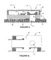
- FIGS. 4 and 5the final form of the product is a silicon condenser microphone package 10 which would most likely be attached to an end user's PCB 28 via a solder reflow process.
- FIG. 5illustrates a method of enlarging the back volume 18 by including a chamber 32 within the end user's circuit board 28 .
- FIGS. 7-10Another embodiment of a silicon condenser microphone package 40 of the present invention is illustrated in FIGS. 7-10 .
- a housing 42is formed from layers of materials, such as those used in providing circuit boards. Accordingly, the housing 42 generally comprises alternating layers of conductive and non-conductive materials 44 , 46 .
- the non-conductive layers 46are typically FR-4 board.
- the conductive layers 44are typically copper.
- This multi-layer housing constructionadvantageously permits the inclusion of circuitry, power and ground planes, solder pads, ground pads, capacitance layers and plated through holes pads within the structure of the housing itself.
- the conductive layersprovide EMI shielding while also allowing configuration as capacitors and/or inductors to filter input/output signals and/or the input power supply.
- the housing 42includes a top portion 48 and a bottom portion 50 spaced by a side portion 52 .
- the housing 42further includes an aperture or acoustic port 54 for receiving an acoustic signal and an inner chamber 56 which is adapted for housing a transducer unit 58 , typically a silicon die microphone or a ball grid array package (BGA).
- the top, bottom, and side portions 48 , 50 , 52are electrically connected, for example with a conductive adhesive 60 .
- the conductive adhesivemay be provided conveniently in the form of suitably configured sheets of dry adhesive disposed between the top, bottom and side portions 48 , 50 and 52 .
- the sheet of dry adhesivemay be activated by pressure, heat or other suitable means after the portions are brought together during assembly.
- Each portionmay comprise alternating conductive and non-conductive layers of 44 , 46 .
- the chamber 56may include an inner lining 61 .
- the inner lining 61is primarily formed by conductive material. It should be understood that the inner lining may include portions of non-conductive material, as the conductive material may not fully cover the non-conductive material.
- the inner lining 61protects the transducer 58 against electromagnetic interference and the like, much like a faraday cage.
- the inner lining 61may also be provided by suitable electrically coupling together of the various conductive layers within the top, bottom and side portions 48 , 50 and 52 of the housing.
- the portions of the housing 42 that include the aperture or acoustic port 54further include a layer of material that forms an environmental barrier 62 over or within the aperture 54 .
- This environmental barrier 62is typically a polymeric material formed to a film, such as a polytetrafluoroethylene (PTFE) or a sintered metal.
- the environmental barrier 62is supplied for protecting the chamber 56 of the housing 42 , and, consequently, the transducer unit 58 within the housing 42 , from environmental elements such as sunlight, moisture, oil, dirt, and/or dust.
- the environmental barrier 62will also have inherent acoustic properties, e.g. acoustic damping/resistance.
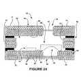
- the environmental barrier 62is chosen such that its acoustic properties cooperate with the transducer unit 58 to enhance the performance of the microphone. This is particularly true in connection with the embodiments illustrated in FIGS. 24 and 25 , which may be configured to operate as directional microphones.
- the environmental barrier layer 62is generally sealed between layers of the portion, top 48 or bottom 50 in which the acoustic port 54 is formed.
- the environmental barriermay be secured between layers of conductive material 44 thereby permitting the layers of conductive material 44 to act as a capacitor (with electrodes defined by the metal) that can be used to filter input and output signals or the input power.
- the environmental barrier layer 62may further serve as a dielectric protective layer when in contact with the conductive layers 44 in the event that the conductive layers also contain thin film passive devices such as resistors and capacitors.
- the barrier layer 62allows subsequent wet processing, board washing of the external portions of the housing 42 , and electrical connection to ground from the walls via thru hole plating.
- the environmental barrier layer 62also allows the order of manufacturing steps in the fabrication of the printed circuit board-based package to be modified. This advantage can be used to accommodate different termination styles. For example, a double sided package can be fabricated having a pair of apertures 54 (see FIG. 25 ), both including an environmental barrier layer 62 . The package would look and act the same whether it is mounted face up or face down, or the package could be mounted to provide directional microphone characteristics.
- the environmental barrier layer 62may also be selected so that its acoustic properties enhance the directional performance of the microphone.
- the transducer unit 58is generally not mounted to the top portion 48 of the housing. This definition is independent of the final mounting orientation to an end user's circuit board. It is possible for the top portion 48 to be mounted face down depending on the orientation of the transducer 58 as well as the choice for the bottom portion 50 .
- the conductive layers 44 of the top portion 48may be patterned to form circuitry, ground planes, solder pads, ground pads, capacitors and plated through hole pads. Referring to FIGS. 1-13 there may be additional alternating conductive layers 44 , non-conductive layers 46 , and environmental protective membranes 62 as the package requires. Alternatively, some layers may be deliberately excluded as well.
- the first non-conductive layer 46may be patterned so as to selectively expose certain features on the first conductive layer 44 .
- FIG. 11illustrates an alternative top portion 48 for a microphone package.
- a connection between the layerscan be formed to provide a conduit to ground.
- the top portion of FIG. 11includes ground planes and/or pattern circuitry 64 and the environmental barrier 62 .
- the ground planes and or pattern circuitry 64are connected by pins 65 .
- FIG. 12illustrates another embodiment of a top portion 48 .
- this embodimentincludes conductive bumps 66 (e.g. Pb/Sn or Ni/Au) patterned on the bottom side to allow secondary electrical contact to the transducer 58 .
- conductive circuitrywould be patterned such that electrical connection between the bumps 66 and a plated through hole termination is made.
- FIG. 13illustrates yet another embodiment of the top portion 48 .
- the top portion 48does not include an aperture or acoustic port 54 .
- the bottom portion 50is the component of the package to which the transducer 58 is primarily mounted. This definition is independent of the final mounting orientation to the end user's circuit board. It is possible for the bottom portion 50 to be mounted facing upwardly depending on the mounting orientation of the transducer 58 as well as the choice for the top portion 48 construction.
- the conductive layers 44 of the bottom portion 50may be patterned to form circuitry, ground planes, solder pads, ground pads, capacitors and plated through hole pads. As shown in FIGS. 14-18 , there may be additional alternating conductive layers 44 , non-conductive layers 46 , and environmental protective membranes 62 as the package requires. Alternatively, some layers may be deliberately excluded as well.
- the first non-conductive layer 46may be patterned so as to selectively expose certain features on the first conductive layer 44 .
- the bottom portion 50comprises a laminated, multi-layered board including layers of conductive material 44 deposited on layers of non-conductive material 46 .
- the first layer of conductive materialis used to attach wire bonds or flip chip bonds. This layer includes etched portions to define lead pads, bond pads, and ground pads. The pads would have holes drilled through them to allow the formation of plated through-holes.
- a dry film 68 of non-conductive materialcovers the conductive material.
- This illustrationshows the exposed bonding pads as well as an exposed ground pad. The exposed ground pad would come in electrical contact with the conductive epoxy and form the connection to ground of the side portion 52 and the base portion 50 .
- ground layerscan be embedded within the base portion 50 .
- the hatched arearepresents a typical ground plane 64 .
- the ground planesdo not overlap the power or output pads, but will overlap the transducer 58 .
- the bottom portion 50 of this embodimentincludes a solder mask layer 68 and alternating layers of conductive and non-conductive material 44 , 46 .
- the bottom portionfurther comprises solder pads 70 for electrical connection to an end user's board.
- FIGS. 16 and 17illustrate embodiments of the bottom portion 50 with enlarged back volumes 18 . These embodiments illustrate formation of the back volume 18 using the conductive/non-conductive layering.
- FIG. 18shows yet another embodiment of the bottom portion 50 .
- the back portion 50includes the acoustic port 54 and the environmental barrier 62 .
- the side portion 52is the component of the package that joins the bottom portion 50 and the top portion 48 .
- the side portion 52may include a single layer of a non-conductive material 46 sandwiched between two layers of conductive material 44 .
- the side portion 52forms the internal height of the chamber 56 that houses the transducer 58 .
- the side portion 52is generally formed by one or more layers of circuit board material, each having a routed window 72 (see FIG. 19 ).
- the side portion 52includes inner sidewalls 74 .
- the inner sidewalls 74are generally plated with a conductive material, typically copper, as shown in FIGS. 20 and 21 .
- the sidewalls 74are formed by the outer perimeter of the routed window 72 and coated/metallized with a conductive material.
- the sidewalls 74may be formed by may alternating layers of non-conductive material 46 and conductive material 44 , each having a routed window 72 (see FIG. 19 ).
- the outer perimeter of the window 72may not require coverage with a conductive material because the layers of conductive material 44 would provide effective shielding.
- FIGS. 23-26illustrate various embodiments of the microphone package 40 . These embodiments utilize top, bottom, and side portions 48 , 50 , and 52 which are described above. It is contemplated that each of the top, bottom, and side portion 48 , 50 , 52 embodiments described above can be utilized in any combination without departing from the invention disclosed and described herein.
- connection to an end user's boardis made through the bottom portion 50 .
- the package mounting orientationis bottom portion 50 down.
- Connection from the transducer 58 to the plated through holesis be made by wire bonding.
- the transducer back volume 18is formed by the back hole (mounted down) of the silicon microphone only. Bond pads, wire bonds and traces to the terminals are not shown. A person of ordinary skilled in the art of PCB design will understand that the traces reside on the first conductor layer 44 .
- the wire bonds from the transducer 58are be connected to exposed pads. The pads are connected to the solder pads via plated through holes and traces on the surface.
- connection to the end user's boardis also made through the bottom portion 50 .
- the package mounting orientationis bottom portion 50 .
- Connection from the transducer 58 to the plated through holesare made by wire bonding.
- the back volumeis formed by a combination of the back hole of the transducer 58 (mounted down) and the bottom portion 50 .
- connection to the end user's boardis also made through the bottom portion 50 .
- the package mounting orientationis bottom portion 50 .
- Connection from the transducer 58 to the plated through holesare made by wire bonding. With acoustic ports 54 on both sides of the package, there is no back volume. This method is suitable to a directional microphone.
- connection to the end user's boardis made through the top portion 48 or the bottom portion 53 .
- the package mounting orientationis either top portion 48 down or bottom portion 50 down.
- Connection from the transducer 58 to the plated through holesis made by flip chipping or wire bonding and trace routing.
- the back volume 18is formed by using the air cavity created by laminating the bottom portion 50 and the top portion 48 together. Some portion of the package fabrication is performed after the transducer 58 has been attached. In particular, the through hole formation, plating, and solder pad definition would be done after the transducer 58 is attached.
- the protective membrane 62is hydrophobic and prevents corrosive plating chemistry from entering the chamber 56 .
- the portion to which the transducer unit 58 is mountedmay include a retaining ring 84 .
- the retaining ring 84prevents wicking of an epoxy 86 into the transducer 58 and from flowing into the acoustic port or aperture 54 . Accordingly, the shape of the retaining ring 84 will typically match the shape of the transducer 58 foot print.
- the retaining ring 84comprises a conductive material (e.g., 3 mil. thick copper) imaged on a non-conductive layer material.
- the retaining ring 84is imaged onto a nonconductive layer.
- An epoxyis applied outside the perimeter of the retaining ring 84 , and the transducer 58 is added so that it overlaps the epoxy 86 and the retaining ring 84 . This reduces epoxy 86 wicking up the sides of the transducer's 58 etched port (in the case of a silicon die microphone).
- the retaining ring 84can be located so that the transducer 58 does not contact the retaining ring 84 .
- the retaining ring 84is slightly smaller than the foot print of the transducer 58 so that the epoxy 86 has a restricted path and is, thus, less likely to wick.
- the retaining ring 84is fabricated so that it contacts the etched port of the transducer 58 .
- Table 5describes the formation of the side portion 52 . This process involves routing a matrix of openings in FR-4 board.
- punchingis thought to be the cost effective method for manufacturing. The punching may done by punching through the entire core, or, alternatively, punching several layers of no-flow pre-preg and thin core c-stage which are then laminated to form the wall of proper thickness.
- the boardAfter routing the matrix, the board will have to be electroless or DM plated. Finally, the boards will have to be routed to match the bottom portion. This step can be done first or last. It may make the piece more workable to perform the final routing as a first step.
- Table 6describes the processing of the top portion.
- the formation of the top portion 48involves imaging a dry film cover lay or liquid solder mask on the bottom (i.e. conductive layer forming the inner layer.
- the exposed layer of the top portion 48will not have a copper coating. It can be processed this way through etching or purchased this way as a one sided laminate.
- a matrix of holesis drilled into the lid board. Drilling may occur after the imaging step. If so, then a suitable solder mask must be chosen that can survive the drilling process.
- FIG. 30is a plan view illustrating a panel 90 for forming a plurality of microphone packages 92 .
- the microphone packages 92are distributed on the panel 90 in a 14 ⁇ 24 array, or 336 microphone packages total. Fewer or more microphone packages may be disposed on the panel 90 , or on smaller or larger panels.
- the microphone packagesinclude a number of layers, such as top, bottom and side portions of the housing, environmental barriers, adhesive layers for joining the portions, and the like. To assure alignment of the portions as they are brought together, each portion may be formed to include a plurality of alignment apertures 94 . To simultaneously manufacture several hundred or even several thousand microphones, a bottom layer, such as described herein, is provided.
- a transducer, amplifier and componentsare secured at appropriate locations on the bottom layer corresponding to each of the microphones to be manufactured.
- An adhesive layersuch as a sheet of dry adhesive is positioned over the bottom layer, and a sidewall portion layer is positioned over the adhesive layer.
- An additional dry adhesive layeris positioned, followed by an environmental barrier layer, another dry adhesive layer and the top layer.
- the dry adhesive layersare activated, such as by the application of heat and/or pressure.
- the panelis then separated into individual microphone assemblies using known panel cutting and separating techniques.
- the microphone, microphone package and method of assembly herein describedfurther allow the manufacture of multiple microphone assembly, such as microphone pairs.
- two microphonesmay be left joined together, such as the microphone pair 96 shown in FIG. 31 .
- Each microphone 98 and 100 of the microphone pair 96is thus a separate, individually operable microphone in a single package sharing a common sidewall 102 .
- conductive tracesmay be formed in the various layers of either the top or bottom portion thus allowing multiple microphones to be electrically coupled.
Landscapes
- Engineering & Computer Science (AREA)
- Microelectronics & Electronic Packaging (AREA)
- Physics & Mathematics (AREA)
- Signal Processing (AREA)
- Acoustics & Sound (AREA)
- Computer Hardware Design (AREA)
- Manufacturing & Machinery (AREA)
- General Physics & Mathematics (AREA)
- Power Engineering (AREA)
- Condensed Matter Physics & Semiconductors (AREA)
- Health & Medical Sciences (AREA)
- Chemical & Material Sciences (AREA)
- Electromagnetism (AREA)
- Otolaryngology (AREA)
- Analytical Chemistry (AREA)
- General Health & Medical Sciences (AREA)
- Toxicology (AREA)
- Ceramic Engineering (AREA)
- Electrostatic, Electromagnetic, Magneto- Strictive, And Variable-Resistance Transducers (AREA)
- Pressure Sensors (AREA)
Abstract
Description
This application is a continuation of U.S. patent application Ser. No. 13/286,558 (now U.S. Pat. No. 8,358,004), filed Nov. 1, 2011, which is a continuation of U.S. patent application Ser. No. 13/111,537 (now U.S. Pat. No. 8,121,331), filed May 19, 2011, which is a continuation of U.S. patent application Ser. No. 11/741,881 (now U.S. Pat. No. 8,018,049), filed Apr. 30, 2007, which is a divisional of U.S. patent application Ser. No. 10/921,747 (now U.S. Pat. No. 7,434,305), filed Aug. 19, 2004, which is a continuation-in-part of U.S. patent application Ser. No. 09/886,854 (now U.S. Pat. No. 7,166,910), filed Jun. 21, 2001, which claims the benefit of U.S. Provisional Patent Application No. 60/253,543, filed Nov. 28, 2000. U.S. patent application Ser. No. 13/668,035, filed Nov. 2, 2012, U.S. patent application Ser. No. 13/668,103, filed Nov. 2, 2012, U.S. patent application Ser. No. 13/732,120, filed Dec. 31, 2012, U.S. patent application Ser. No. 13/732,205, filed Dec. 31, 2012, U.S. patent application Ser. No. 13/732,232, filed Dec. 31, 2012, and U.S. patent application Ser. No. 13/732,265, filed Dec. 31, 2012, are also continuations of U.S. patent application Ser. No. 13/286,558 (now U.S. Pat. No. 8,358,004). These applications are hereby incorporated by reference herein in their entireties for all purposes.
This patent relates generally to a housing for a transducer. More particularly, this patent relates to a silicon condenser microphone including a housing for shielding a transducer.
There have been a number of disclosures related to building microphone elements on the surface of a silicon die. Certain of these disclosures have come in connection with the hearing aid field for the purpose of reducing the size of the hearing aid unit. While these disclosures have reduced the size of the hearing aid, they have not disclosed how to protect the transducer from outside interferences. For instance, transducers of this type are fragile and susceptible to physical damage. Furthermore, they must be protected from light and electromagnetic interferences. Moreover, they require an acoustic pressure reference to function properly. For these reasons, the silicon die must be shielded.
Some shielding practices have been used to house these devices. For instance, insulated metal cans or discs have been provided. Additionally, DIPs and small outline integrated circuit (SOIC) packages have been utilized. However, the drawbacks associated with manufacturing these housings, such as lead time, cost, and tooling, make these options undesirable.
The present invention is directed to a silicon condenser microphone package that allows acoustic energy to contact a transducer disposed within a housing. The housing provides the necessary pressure reference while at the same time protects the transducer from light, electromagnetic interference, and physical damage. In accordance with an embodiment of the invention a silicon condenser microphone includes a transducer and a substrate and a cover forming the housing. The substrate may have an upper surface with a recess formed therein allowing the transducer to be attached to the upper surface and to overlap at least a portion of the recess thus forming a back volume. The cover is placed over the transducer and includes an aperture adapted for allowing sound waves to reach the transducer.
Other features and advantages of the invention will be apparent from the following specification taken in conjunction with the following drawings.
While the invention is susceptible of embodiments in many different forms, there is shown in the drawings and will herein be described in detail several possible embodiments of the invention with the understanding that the present disclosure is to be considered as an exemplification of the principles of the invention and is not intended to limit the broad aspect of the invention to the embodiments illustrated.
The present invention is directed to microphone packages. The benefits of the microphone packages disclosed herein over microphone packaging utilizing plastic body/lead frames include the ability to process packages in panel form allowing more units to be formed per operation and at much lower cost. The typical lead frame for a similarly functioning package would contain between 40 and 100 devices connected together. The present disclosure would have approximately 14,000 devices connected together (as a panel). Also, the embodiments disclosed herein require minimal “hard-tooling” This allows the process to adjust to custom layout requirements without having to redesign mold, lead frame, and trim/form tooling.
Moreover, many of the described embodiments have a better match of thermal coefficients of expansion with the end user's PCB, typically made of FR-4, since the microphone package is also made primarily of FR-4. These embodiments of the invention may also eliminate the need for wire bonding that is required in plastic body/lead frame packages. The footprint is typically smaller than that would be required for a plastic body/lead frame design since the leads may be formed by plating a through-hole in a circuit board to form the pathway to the solder pad. In a typical plastic body/lead frame design, a (gull wing configuration would be used in which the leads widen the overall foot print.
Now, referring toFIGS. 1-3 , three embodiments of a siliconcondenser microphone package 10 of the present invention are illustrated. Included withinsilicon microphone package 10 is atransducer 12, e.g. a silicon condenser microphone as disclosed in U.S. Pat. No. 5,870,482 which is hereby incorporated by reference and anamplifier 16. The package itself includes asubstrate 14, a back volume orair cavity 18, which provides a pressure reference for thetransducer 12, and acover 20. Thesubstrate 14 may be formed of FR-4 material allowing processing in circuit board panel form, thus taking advantage of economies of scale in manufacturing.FIG. 6 is a plan view of thesubstrate 14 showing theback volume 18 surrounded a plurality of terminal pads.
Theback volume 18 may be formed by a number of methods, including controlled depth drilling of anupper surface 19 of thesubstrate 14 to form a recess over which thetransducer 12 is mounted (FIG. 1 ); drilling and routing of several individual sheets of FR-4 and laminating the individual sheets to form theback volume 18, which may or may not have internal support posts (FIG. 2 ); or drilling completely through thesubstrate 14 and providing a sealingring 22 on the bottom of the device that will seal theback volume 18 during surface mounting to a user's “board”28 (FIGS. 3-5 ). In this example, the combination of the substrate and the user'sboard 28 creates theback volume 18. Theback volume 18 is covered by the transducer12 (e.g., a MEMS device) which may be “bumpbonded” and mounted face down. The boundary is sealed such that theback volume 18 is operably “air-tight.”
Thecover 20 is attached for protection and processability. Thecover 20 contains anaperture 24 which may contain asintered metal insert 26 to prevent water, particles and/or light from entering the package and damaging the internal components inside; i.e. semiconductor chips. Theaperture 24 is adapted for allowing sound waves to reach thetransducer 12. Thesintered metal insert 26 will also have certain acoustic properties, e.g. acoustic damping or resistance. Thesintered metal insert 26 may therefore be selected such that its acoustic properties enhance the functional capability of thetransducer 12 and/or the overall performance of thesilicon microphone 10.
Referring toFIGS. 4 and 5 the final form of the product is a siliconcondenser microphone package 10 which would most likely be attached to an end user'sPCB 28 via a solder reflow process.FIG. 5 illustrates a method of enlarging theback volume 18 by including achamber 32 within the end user'scircuit board 28.
Another embodiment of a silicon condenser microphone package40 of the present invention is illustrated inFIGS. 7-10 . In this embodiment, ahousing 42 is formed from layers of materials, such as those used in providing circuit boards. Accordingly, thehousing 42 generally comprises alternating layers of conductive andnon-conductive materials non-conductive layers 46 are typically FR-4 board. Theconductive layers 44 are typically copper. This multi-layer housing construction advantageously permits the inclusion of circuitry, power and ground planes, solder pads, ground pads, capacitance layers and plated through holes pads within the structure of the housing itself. The conductive layers provide EMI shielding while also allowing configuration as capacitors and/or inductors to filter input/output signals and/or the input power supply.
In the embodiment illustrated, thehousing 42 includes atop portion 48 and abottom portion 50 spaced by aside portion 52. Thehousing 42 further includes an aperture oracoustic port 54 for receiving an acoustic signal and aninner chamber 56 which is adapted for housing atransducer unit 58, typically a silicon die microphone or a ball grid array package (BGA). The top, bottom, andside portions conductive adhesive 60. The conductive adhesive may be provided conveniently in the form of suitably configured sheets of dry adhesive disposed between the top, bottom andside portions
Thechamber 56 may include aninner lining 61. Theinner lining 61 is primarily formed by conductive material. It should be understood that the inner lining may include portions of non-conductive material, as the conductive material may not fully cover the non-conductive material. Theinner lining 61 protects thetransducer 58 against electromagnetic interference and the like, much like a faraday cage. Theinner lining 61 may also be provided by suitable electrically coupling together of the various conductive layers within the top, bottom andside portions
In the various embodiments illustrated inFIGS. 7-10 and23-26, the portions of thehousing 42 that include the aperture oracoustic port 54 further include a layer of material that forms anenvironmental barrier 62 over or within theaperture 54. Thisenvironmental barrier 62 is typically a polymeric material formed to a film, such as a polytetrafluoroethylene (PTFE) or a sintered metal. Theenvironmental barrier 62 is supplied for protecting thechamber 56 of thehousing 42, and, consequently, thetransducer unit 58 within thehousing 42, from environmental elements such as sunlight, moisture, oil, dirt, and/or dust. Theenvironmental barrier 62 will also have inherent acoustic properties, e.g. acoustic damping/resistance. Therefore theenvironmental barrier 62 is chosen such that its acoustic properties cooperate with thetransducer unit 58 to enhance the performance of the microphone. This is particularly true in connection with the embodiments illustrated inFIGS. 24 and 25 , which may be configured to operate as directional microphones.
Theenvironmental barrier layer 62 is generally sealed between layers of the portion, top48 or bottom50 in which theacoustic port 54 is formed. For example, the environmental barrier may be secured between layers ofconductive material 44 thereby permitting the layers ofconductive material 44 to act as a capacitor (with electrodes defined by the metal) that can be used to filter input and output signals or the input power. Theenvironmental barrier layer 62 may further serve as a dielectric protective layer when in contact with theconductive layers 44 in the event that the conductive layers also contain thin film passive devices such as resistors and capacitors.
In addition to protecting thechamber 56 from environmental elements, thebarrier layer 62 allows subsequent wet processing, board washing of the external portions of thehousing 42, and electrical connection to ground from the walls via thru hole plating. Theenvironmental barrier layer 62 also allows the order of manufacturing steps in the fabrication of the printed circuit board-based package to be modified. This advantage can be used to accommodate different termination styles. For example, a double sided package can be fabricated having a pair of apertures54 (seeFIG. 25 ), both including anenvironmental barrier layer 62. The package would look and act the same whether it is mounted face up or face down, or the package could be mounted to provide directional microphone characteristics. Moreover, theenvironmental barrier layer 62 may also be selected so that its acoustic properties enhance the directional performance of the microphone.
Referring toFIGS. 7 ,8, and11-13 thetransducer unit 58 is generally not mounted to thetop portion 48 of the housing. This definition is independent of the final mounting orientation to an end user's circuit board. It is possible for thetop portion 48 to be mounted face down depending on the orientation of thetransducer 58 as well as the choice for thebottom portion 50. Theconductive layers 44 of thetop portion 48 may be patterned to form circuitry, ground planes, solder pads, ground pads, capacitors and plated through hole pads. Referring toFIGS. 1-13 there may be additional alternatingconductive layers 44,non-conductive layers 46, and environmentalprotective membranes 62 as the package requires. Alternatively, some layers may be deliberately excluded as well. The firstnon-conductive layer 46 may be patterned so as to selectively expose certain features on the firstconductive layer 44.
Referring toFIGS. 7 ,8 and14-18, thebottom portion 50 is the component of the package to which thetransducer 58 is primarily mounted. This definition is independent of the final mounting orientation to the end user's circuit board. It is possible for thebottom portion 50 to be mounted facing upwardly depending on the mounting orientation of thetransducer 58 as well as the choice for thetop portion 48 construction. Like thetop portion 48, theconductive layers 44 of thebottom portion 50 may be patterned to form circuitry, ground planes, solder pads, ground pads, capacitors and plated through hole pads. As shown inFIGS. 14-18 , there may be additional alternatingconductive layers 44,non-conductive layers 46, and environmentalprotective membranes 62 as the package requires. Alternatively, some layers may be deliberately excluded as well. The firstnon-conductive layer 46 may be patterned so as to selectively expose certain features on the firstconductive layer 44.
Referring toFIGS. 14 athrough14d, thebottom portion 50 comprises a laminated, multi-layered board including layers ofconductive material 44 deposited on layers ofnon-conductive material 46. Referring toFIG. 14 b, the first layer of conductive material is used to attach wire bonds or flip chip bonds. This layer includes etched portions to define lead pads, bond pads, and ground pads. The pads would have holes drilled through them to allow the formation of plated through-holes.
As shown inFIG. 14 c, adry film 68 of non-conductive material covers the conductive material. This illustration shows the exposed bonding pads as well as an exposed ground pad. The exposed ground pad would come in electrical contact with the conductive epoxy and form the connection to ground of theside portion 52 and thebase portion 50.
Referring toFIG. 14 d, ground layers can be embedded within thebase portion 50. The hatched area represents atypical ground plane 64. The ground planes do not overlap the power or output pads, but will overlap thetransducer 58.
Referring toFIG. 15 , an embodiment of thebottom portion 50 is illustrated. Thebottom portion 50 of this embodiment includes asolder mask layer 68 and alternating layers of conductive andnon-conductive material solder pads 70 for electrical connection to an end user's board.
Referring toFIGS. 7-10 and19-22, theside portion 52 is the component of the package that joins thebottom portion 50 and thetop portion 48. Theside portion 52 may include a single layer of anon-conductive material 46 sandwiched between two layers ofconductive material 44. Theside portion 52 forms the internal height of thechamber 56 that houses thetransducer 58. Theside portion 52 is generally formed by one or more layers of circuit board material, each having a routed window72 (seeFIG. 19 ).
Referring toFIGS. 19-22 , theside portion 52 includesinner sidewalls 74. Theinner sidewalls 74 are generally plated with a conductive material, typically copper, as shown in FIGS.20 and21. Thesidewalls 74 are formed by the outer perimeter of the routedwindow 72 and coated/metallized with a conductive material.
Alternatively, thesidewalls 74 may be formed by may alternating layers ofnon-conductive material 46 andconductive material 44, each having a routed window72 (seeFIG. 19 ). In this case, the outer perimeter of thewindow 72 may not require coverage with a conductive material because the layers ofconductive material 44 would provide effective shielding.
InFIG. 23 , connection to an end user's board is made through thebottom portion 50. The package mounting orientation isbottom portion 50 down. Connection from thetransducer 58 to the plated through holes is be made by wire bonding. The transducer backvolume 18 is formed by the back hole (mounted down) of the silicon microphone only. Bond pads, wire bonds and traces to the terminals are not shown. A person of ordinary skilled in the art of PCB design will understand that the traces reside on thefirst conductor layer 44. The wire bonds from thetransducer 58 are be connected to exposed pads. The pads are connected to the solder pads via plated through holes and traces on the surface.
InFIG. 24 , connection to the end user's board is also made through thebottom portion 50. Again, the package mounting orientation isbottom portion 50. Connection from thetransducer 58 to the plated through holes are made by wire bonding. The back volume is formed by a combination of the back hole of the transducer58 (mounted down) and thebottom portion 50.
InFIG. 25 , connection to the end user's board is also made through thebottom portion 50. Again, the package mounting orientation isbottom portion 50. Connection from thetransducer 58 to the plated through holes are made by wire bonding. Withacoustic ports 54 on both sides of the package, there is no back volume. This method is suitable to a directional microphone.
InFIG. 26 , connection to the end user's board is made through thetop portion 48 or the bottom portion53. The package mounting orientation is eithertop portion 48 down orbottom portion 50 down. Connection from thetransducer 58 to the plated through holes is made by flip chipping or wire bonding and trace routing. Theback volume 18 is formed by using the air cavity created by laminating thebottom portion 50 and thetop portion 48 together. Some portion of the package fabrication is performed after thetransducer 58 has been attached. In particular, the through hole formation, plating, and solder pad definition would be done after thetransducer 58 is attached. Theprotective membrane 62 is hydrophobic and prevents corrosive plating chemistry from entering thechamber 56.
Referring toFIGS. 27-29 , the portion to which thetransducer unit 58 is mounted may include a retainingring 84. The retainingring 84 prevents wicking of an epoxy86 into thetransducer 58 and from flowing into the acoustic port oraperture 54. Accordingly, the shape of the retainingring 84 will typically match the shape of thetransducer 58 foot print. The retainingring 84 comprises a conductive material (e.g., 3 mil. thick copper) imaged on a non-conductive layer material.
Referring toFIG. 27 , the retainingring 84 is imaged onto a nonconductive layer. An epoxy is applied outside the perimeter of the retainingring 84, and thetransducer 58 is added so that it overlaps the epoxy86 and the retainingring 84. This reduces epoxy86 wicking up the sides of the transducer's58 etched port (in the case of a silicon die microphone).
Alternatively, referring toFIG. 28 , the retainingring 84 can be located so that thetransducer 58 does not contact the retainingring 84. In this embodiment, the retainingring 84 is slightly smaller than the foot print of thetransducer 58 so that the epoxy86 has a restricted path and is, thus, less likely to wick. InFIG. 29 , the retainingring 84 is fabricated so that it contacts the etched port of thetransducer 58. The following tables provide an illustrative example of a typical circuit board processing technique for fabrication of the housing of this embodiment.
| TABLE 1 |
| Materials |
| Material | Component | Note | ||
| 1 | 0.5/0.5 oz. DST | Bottom Portion | ||
| Cu 5 core FR-4 | (Conductive Layers Non- | |||
| Conductive Layer 1) | ||||
| 2 | 0.5/0.5 oz. DST | Bottom Portion | ||
| Cu 5 core FR-4 | (Conductive Layers | |||
| 3 and 4; Non-Conductive | ||||
| Layer 2) | ||||
| 3 | 106 pre-preg | For | ||
| Material | ||||
| 1 and | ||||
| Material 2 | ||||
| 4 | 0.5/0.5 oz. DST | Side Portion | Metallized | |
| Cu 40 Core FR-4 | Afterward | |||
| 5 | Bare/0.5 oz. Cu 2 | Top Portion | ||
| core FR-4 (2 | (Each Piece Includes 1 | |||
| pieces) | Conductive and 1 | |||
| Non-Conductive Layer) | ||||
| 6 | Expanded PTFE | Environmental Barrier | ||
| TABLE 2 |
| Processing of Materials (Base Portion Material 1) |
| Step | Description | Note | ||
| 1 | Dry Film | |||
| Conductive Layers | ||||
| 2 | Expose | Mask Material 1 (Upper | Forms Ground | |
| Conductive Layer) | Plane on | |||
| Conductive Layer | ||||
| 3 | Develop | |||
| 4 | Etch Cu | No Etching on | ||
| Upper Conductive | ||||
| Layer | ||||
| 5 | Strip Dry Film | |||
| TABLE 3 |
| Processing of Materials (Bottom Portion Material 2) |
| Step | Description | Note | ||
| 1 | Dry Film | |||
| Conductive Layers | ||||
| 2 | Expose | Mask Material 2 (Upper | Forms Ground | |
| Conductive Layer) | Plane on | |||
| Conductive Layer | ||||
| 3 | Develop | |||
| 4 | Etch Cu | No Etching on Upper | ||
| Conductive | ||||
| Layer | ||||
| 5 | Strip Dry Film | |||
| TABLE 4 |
| Processing of |
| Step | Description | Note | ||
| 1 | Materials | 1 and 2 | ||
| Laminated Using | ||||
| 2 | Drill Thru Holes | Drill Bit = 0.025 in. | ||
| 3 | Direct | Plates Thru Holes | ||
| Metallization/Flash | ||||
| Copper | ||||
| 4 | Dry Film (L1 and L4) | |||
| 5 | Expose | Mask Laminated | Forms Traces | |
| and Solder Pads | ||||
| (Upper and Lower | ||||
| Conductive Layers) | ||||
| 6 | Develop | |||
| 7 | Electrolytic Cu | 1.0 mil | ||
| 8 | Electrolytic Sn | As Required | ||
| 9 | ||||
| 10 | Etch Cu | |||
| 11 | ||||
| 12 | Insert Finishing | NG Option (See | NG Option for | |
| Option Here | Table Below) | Proof of Principle | ||
| 13 | Dry Film (cover | 2.5 mil | Minimum Thickness | |
| lay) on Upper | on Upper Conductive | |||
| Conductive Layer | Layer | |||
| Only | ||||
| 14 | Expose | Mask Laminated | This mask defines an | |
| area on the upper | ||||
| (upper and lower) | conductive layer that | |||
| will receive a dry film | ||||
| solder mask (cover | ||||
| lay). The bottom layer | ||||
| will not have dry film | ||||
| applied to it. The | ||||
| plated through holes | ||||
| will be bridged | ||||
| over by the coating | ||||
| on the top. | ||||
| 15 | ||||
| 16 | Cure | Full Cure | ||
| 17 | Route Panels | Route Bit = As | Forms 4″ × 4″ pieces. | |
| Required | Conforms to finished | |||
| dims | ||||
Table 5 describes the formation of theside portion 52. This process involves routing a matrix of openings in FR-4 board. However, punching is thought to be the cost effective method for manufacturing. The punching may done by punching through the entire core, or, alternatively, punching several layers of no-flow pre-preg and thin core c-stage which are then laminated to form the wall of proper thickness.
After routing the matrix, the board will have to be electroless or DM plated. Finally, the boards will have to be routed to match the bottom portion. This step can be done first or last. It may make the piece more workable to perform the final routing as a first step.
| TABLE 5 |
| Processing of Material 4 (Side Portion) |
| Step | Description | Note | ||
| 1 | Route/Punch | Route Bit = 0.031 in. | Forms Side Portion | |
| Matrix of | ||||
| Openings | ||||
| 2 | Direct | 0.25 mil minimum | Forms Sidewalls | |
| Metallization/ | on Side | |||
| Flash Cu | ||||
| 3 | Route Panels | |||
Table 6 describes the processing of the top portion. The formation of thetop portion 48 involves imaging a dry film cover lay or liquid solder mask on the bottom (i.e. conductive layer forming the inner layer. The exposed layer of thetop portion 48 will not have a copper coating. It can be processed this way through etching or purchased this way as a one sided laminate.
A matrix of holes is drilled into the lid board. Drilling may occur after the imaging step. If so, then a suitable solder mask must be chosen that can survive the drilling process.
| TABLE 6 |
| Processing of Top Portion |
| Step | Description | Note | ||
| 1 | Dry Film | Conductive Layer | ||
| 2 | Expose | Mask Bare Layer | ||
| 3 | Develop | |||
| 4 | Cure | |||
| 5 | Drill Matrix of | Drill Bit 0.025 in. | Acoustic Ports | |
| Holes | ||||
| 6 | Laminate | PTFE (Environmental | Forms Top Portion | |
| Barrier) Between 2 Pieces | ||||
| of Material 5 | ||||
| TABLE 7 |
| Processing of |
| Step | Description | Note | ||
| 1 | Screen | |||
| Conductive | ||||
| Adhesive on | ||||
| Material 4 | ||||
| 2 | Laminate | Bottom Portion with Side | Forms Bottom | |
| Portion | Portion with Side | |||
| Portion (spacer) | ||||
| 3 | Add Transducer | Silicon Die Microphone | ||
| Assembly | and Integrated Circuit | |||
| TABLE 8 |
| Processing of |
| Step | Description | Note | ||
| 1 | Screen | |||
| Conductive | ||||
| Adhesive on | ||||
| Top Portion | ||||
| 2 | Laminate | Bottom Portion and Side | Forms Housing | |
| Portion with | ||||
| 3 | Dice | |||
| TABLE 9 |
| Finishing Option NG (Nickel/Gold) |
| Step | Description | Note | |||
| 1 | Immersion Ni | ||||
| (40-50 μ-in) | |||||
| 2 | Immersion Au | ||||
| (25-30 μ-in) | |||||
| TABLE 10 |
| Finishing Option NGT (Nickel/Gold/Tin) |
| Type | |||
| 1 | Mask L2 (using thick dry film or high tack dicing tape) | ||
| 2 | Immersion Ni (40-50 μ-in) | ||
| 3 | Immersion Au (25-30 μ-in) | ||
| 4 | Remove Mask on L2 | ||
| 5 | Mask L1 (using thick dry film or high tack dicing tape) | ||
| bridge over cavity created by wall | |||
| 6 | Immersion Sn (100-250 μ-in) | ||
| 7 | Remove Mask on L1 | ||
| TABLE 11 |
| Finishing Option ST (Silver/Tin) |
| Type | |||
| 1 | Mask L2 (using thick dry film or high tack dicing tape) | ||
| 2 | Immersion Ag (40-50 μ-in) | ||
| 3 | Remove Mask on L2 | ||
| 4 | Mask L1 (using thick dry film or high tack dicing tape) | ||
| bridge over cavity created by wall | |||
| 5 | Immersion Sn (100-250 μ-in) | ||
| 6 | Remove Mask on L1 | ||
The microphone, microphone package and method of assembly herein described further allow the manufacture of multiple microphone assembly, such as microphone pairs. In the simplest form, during separation two microphones may be left joined together, such as themicrophone pair 96 shown inFIG. 31 . Eachmicrophone microphone pair 96 is thus a separate, individually operable microphone in a single package sharing acommon sidewall 102. Alternatively, as described herein, conductive traces may be formed in the various layers of either the top or bottom portion thus allowing multiple microphones to be electrically coupled.
While specific embodiments have been illustrated and described, numerous modifications come to mind without significantly departing from the spirit of the invention, and the scope of protection is only limited by the scope of the accompanying Claims.
Claims (30)
1. A solder reflow surface mount microelectromechanical system (MEMS) microphone device comprising:
a substrate having a planar upper surface and a planar lower surface, the upper surface having an interior region and a peripheral region that completely surrounds the interior region, each substrate further comprising:
a first plurality of metal pads formed on the upper surface of the substrate;
a second plurality of metal pads formed on the lower surface of the substrate and arranged within a perimeter of the lower surface of the substrate, wherein the second plurality of metal pads are configured to mechanically attach and electrically couple the surface mount MEMS microphone device to pads on a surface of an external printed circuit board; and
one or more electrical pathways formed completely within the substrate, wherein the pathways electrically couple one or more of the first plurality of metal pads on the upper surface of the substrate to one or more of the second plurality of metal pads on the lower surface of the substrate;
a MEMS microphone die mounted to the upper surface of the substrate and electrically coupled to at least one of the first plurality of metal pads on the upper surface of the substrate; and
a single-piece cover that has a top region with an acoustic port that passes completely through the cover, and a sidewall region, the sidewall region adjoining the top region at a substantially perpendicular angle and having a predetermined height, an exterior surface, an interior surface, and a bottom surface,
wherein the bottom surface of the sidewall region is aligned with and attached to the peripheral region of the upper surface of the substrate, thereby forming a protective enclosure for the MEMS microphone die that reduces electromagnetic interference, and
wherein the predetermined height and interior surface of the sidewall region and interior surface of the top region, in cooperation with the interior region of the upper surface of the substrate, defines an acoustic chamber for the MEMS microphone die.
2. A surface mount MEMS microphone device according toclaim 1 , wherein the one or more electrical pathways are plated through-holes electrically coupling one or more of the first plurality of metal pads to one or more of the second plurality of metal pads.
3. A surface mount MEMS microphone device according toclaim 1 , further comprising a metal pad formed on the upper surface of the substrate, wherein the MEMS microphone die is mounted to the metal pad.
4. A surface mount MEMS microphone device according toclaim 1 , wherein the substrate comprises FR-4 material.
5. A surface mount MEMS microphone device according toclaim 1 , further comprising at least one passive electrical device formed within the substrate.
6. A surface mount MEMS microphone device according toclaim 1 , wherein the enclosure protects the MEMS microphone die from at least one of light and physical damage.
7. A surface mount MEMS microphone device according toclaim 6 , wherein the enclosure further comprises acoustic material that substantially blocks environmental contaminants from entering the chamber through the acoustic port.
8. A surface mount MEMS microphone device according toclaim 1 , wherein a diaphragm of the MEMS microphone die defines a front volume and a back volume in the acoustic chamber, and the acoustic port formed in the cover is acoustically coupled to the front volume.
9. A surface mount microelectromechanical system (MEMS) microphone device comprising:
a printed circuit board comprising multiple layers of non-conductive material and having a planar upper surface and a planar lower surface, the upper surface having an interior region and a peripheral region that completely surrounds the interior region, the printed circuit board comprising:
a first plurality of metal pads formed on the upper surface of the printed circuit board;
a second plurality of metal pads formed on the lower surface of the printed circuit board and arranged within a perimeter of the lower surface of the printed circuit board, wherein the second plurality of metal pads are configured to mechanically attach and electrically couple the surface mount MEMS microphone device to pads on a surface of an external printed circuit board; and
one or more electrical pathways formed completely within the printed circuit board, wherein the pathways electrically couple one or more of the first plurality of metal pads on the upper surface of the printed circuit board to one or more of the second plurality of metal pads on the lower surface of the printed circuit board;
a MEMS microphone die mounted to the upper surface of the printed circuit board and electrically coupled to at least one of the first plurality of metal pads on the upper surface of the printed circuit board; and
a single-piece cover that has a top region with an acoustic port that passes completely through the cover, and a sidewall region, the sidewall region adjoining the top region at a substantially perpendicular angle and having a predetermined height, an exterior surface, an interior surface, and a bottom surface,
wherein the bottom surface of the sidewall region is aligned with and mechanically attached to the peripheral region of the upper surface of the printed circuit board, thereby forming a protective enclosure for the MEMS microphone die that reduces electromagnetic interference, and
wherein the predetermined height and interior surface of the sidewall region, in cooperation with the interior surface of the top region, defines an acoustic chamber for the MEMS microphone die;
wherein the cover has a first length and a first width, and the printed circuit board has a second length and a second width; and
wherein the first length of the cover and second length of the printed circuit board are substantially equal, and the first width of the cover and second width of the printed circuit board are substantially equal.
10. A surface mount MEMS microphone device according toclaim 9 , wherein the one or more electrical pathways are plated through-holes electrically coupling one or more of the first plurality of metal pads to one or more of the second plurality of metal pads.
11. A surface mount MEMS microphone device according toclaim 9 , further comprising a metal pad formed on the upper surface of the printed circuit board, wherein the MEMS microphone die is mounted to the metal pad.
12. A surface mount MEMS microphone device according toclaim 9 , wherein the printed circuit board comprises FR-4 material.
13. A surface mount MEMS microphone device according toclaim 9 , further comprising at least one passive electrical device formed within the printed circuit board.
14. A surface mount MEMS microphone device according toclaim 9 , wherein the enclosure protects the MEMS microphone die from at least one of light and physical damage.
15. A surface mount MEMS microphone device according toclaim 9 , wherein the enclosure further comprises acoustic material that substantially blocks environmental contaminants from entering the acoustic chamber through the acoustic port.
16. A surface mount MEMS microphone device according toclaim 9 , wherein a diaphragm of the MEMS microphone die defines a front volume and a back volume in the acoustic chamber, and the acoustic port formed in the cover is acoustically coupled to the front volume.
17. A surface mount microelectromechanical system (MEMS) microphone device comprising:
a substrate comprising multiple layers of non-conductive material and having a planar upper surface and a planar lower surface, the upper surface having an interior region and a peripheral region that completely surrounds the interior region, the substrate further comprising:
a first plurality of metal pads formed on the upper surface of the substrate;
a second plurality of metal pads formed on the lower surface of the substrate and arranged within a perimeter of the lower surface of the substrate, wherein the second plurality of metal pads are configured to mechanically couple and electrically couple the surface mount MEMS microphone device to pads on a surface of an external printed circuit board; and
one or more electrical pathways formed completely within the substrate, wherein the pathways electrically couple one or more of the first plurality of metal pads on the upper surface of the substrate to one or more of the second plurality of metal pads on the lower surface of the substrate;
a MEMS microphone die physically coupled to the upper surface of the substrate and electrically coupled to at least one of the first plurality of metal pads on the upper surface of the substrate; and
a single-piece cover that has a top region with an acoustic port that passes completely through the cover, and a sidewall region, the sidewall region adjoining the top region at a substantially perpendicular angle and having a predetermined height, an exterior surface, an interior surface, and a bottom surface,
wherein the bottom surface of the sidewall region is aligned with and physically coupled to the peripheral region of the upper surface of the substrate, thereby forming a protective enclosure for the MEMS microphone die that reduces electromagnetic interference, and
wherein the interior of the protective enclosure is an acoustic chamber having a volume defined by the predetermined height of sidewall region, and the width and length of the top region of the cover.
18. A surface mount MEMS microphone device according toclaim 17 , wherein the one or more electrical pathways are plated through-holes electrically coupling one or more of the first plurality of metal pads to one or more of the second plurality of metal pads.
19. A surface mount MEMS microphone device according toclaim 17 , further comprising a metal pad formed on the upper surface of the substrate, wherein the MEMS microphone die is physically coupled to the metal pad.
20. A surface mount MEMS microphone device according toclaim 17 , wherein the substrate comprises FR-4 material.
21. A surface mount MEMS microphone device according toclaim 17 , further comprising at least one passive electrical device formed within the substrate.
22. A surface mount MEMS microphone device according toclaim 17 , wherein the enclosure protects the MEMS microphone die from at least one of light and physical damage.
23. A surface mount MEMS microphone device according toclaim 17 , wherein the enclosure further comprises acoustic material that substantially blocks environmental contaminants from entering the acoustic chamber through the acoustic port.
24. A surface mount MEMS microphone device according toclaim 17 , wherein a diaphragm of the MEMS microphone die defines a front volume and a back volume in the acoustic chamber, and the acoustic port formed in the cover is acoustically coupled to the front volume.
25. A surface mount MEMS microphone device according toclaim 17 , wherein the enclosure protects the MEMS microphone die from at least one of light and physical damage.
26. A surface mount MEMS microphone device according toclaim 17 , wherein the enclosure further comprises acoustic material that substantially blocks environmental contaminants from entering the acoustic chamber through the acoustic port.
27. A surface mount MEMS microphone device according toclaim 17 , wherein a diaphragm of the MEMS microphone die defines a front volume and a back volume in the acoustic chamber, and the port formed in the cover is acoustically coupled to the front volume.
28. A surface mount microelectromechanical system (MEMS) microphone device comprising:
a printed circuit board having a multi-layer core of conductive and non-conductive materials, wherein the printed circuit board has a planar upper surface and a planar lower surface, the upper surface having an interior region and a peripheral region that completely surrounds the interior region, the printed circuit board further comprising:
a first metal layer formed on the upper surface of the printed circuit board and patterned into a first plurality of metal pads, wherein at least one pad of the first plurality of metal pads is formed in the peripheral region of the upper surface of the printed circuit board;
a second metal layer formed on the lower surface of the printed circuit board and patterned into a second plurality of metal pads, the second plurality of metal pads arranged within a perimeter of the lower surface of the printed circuit board, wherein the second plurality of metal pads are configured to mechanically couple and electrically couple the surface mount MEMS microphone device to pads on a surface of an external printed circuit board; and
one or more electrical pathways formed completely within the printed circuit board, wherein the pathways electrically couple one or more of the first plurality of metal pads on the upper surface of the printed circuit board to one or more of the second plurality of metal pads on the lower surface of the printed circuit board;
a MEMS microphone die physically coupled to the upper surface of the multi-layer printed circuit board and electrically coupled to at least one of the first plurality of patterned metal pads; and
a single-piece cover that has a top region with an acoustic port that passes completely through the cover, and a sidewall region, the sidewall region adjoining the top region at a substantially perpendicular angle and having a predetermined height, an exterior sidewall surface, an interior sidewall surface, and a bottom surface,
wherein the bottom surface of the sidewall region is aligned with and physically coupled to the peripheral region of the upper surface of the printed circuit board, thereby forming a protective enclosure for the MEMS microphone die that reduces electromagnetic interference, and
wherein the interior of the protective enclosure is an acoustic chamber having a volume defined by the predetermined height of sidewall region, and the width and length of the top region of the cover.
29. A surface mount MEMS microphone device according toclaim 28 , further comprising a metal pad formed on the upper surface of the printed circuit board, wherein the MEMS microphone die is physically coupled to the metal pad.
30. A surface mount MEMS microphone device according toclaim 28 , further comprising at least one passive electrical device formed within the printed circuit board.
Priority Applications (10)
| Application Number | Priority Date | Filing Date | Title |
|---|---|---|---|
| US13/732,179US8704360B1 (en) | 2000-11-28 | 2012-12-31 | Top port surface mount silicon condenser microphone package |
| US13/838,538US8623709B1 (en) | 2000-11-28 | 2013-03-15 | Methods of manufacture of top port surface mount silicon condenser microphone packages |
| US14/149,525US9051171B1 (en) | 2000-11-28 | 2014-01-07 | Bottom port surface mount MEMS microphone |
| US14/149,373US9156684B1 (en) | 2000-11-28 | 2014-01-07 | Methods of manufacture of top port surface mount MEMS microphones |
| US14/258,870US9148731B1 (en) | 2000-11-28 | 2014-04-22 | Top port surface mount MEMS microphone |
| US14/836,499US9338560B1 (en) | 2000-11-28 | 2015-08-26 | Top port multi-part surface mount silicon condenser microphone |
| US15/135,125US9693133B2 (en) | 2000-11-28 | 2016-04-21 | Top port multi-part surface mount silicon condenser microphone |
| US15/606,686US9980038B2 (en) | 2000-11-28 | 2017-05-26 | Top port multi-part surface mount silicon condenser microphone |
| US15/968,676US10321226B2 (en) | 2000-11-28 | 2018-05-01 | Top port multi-part surface mount MEMS microphone |
| US16/392,546US10477301B2 (en) | 2000-11-28 | 2019-04-23 | Top port multi-part surface mount silicon condenser microphone |
Applications Claiming Priority (7)
| Application Number | Priority Date | Filing Date | Title |
|---|---|---|---|
| US25354300P | 2000-11-28 | 2000-11-28 | |
| US09/886,854US7166910B2 (en) | 2000-11-28 | 2001-06-21 | Miniature silicon condenser microphone |
| US10/921,747US7434305B2 (en) | 2000-11-28 | 2004-08-19 | Method of manufacturing a microphone |
| US11/741,881US8018049B2 (en) | 2000-11-28 | 2007-04-30 | Silicon condenser microphone and manufacturing method |
| US13/111,537US8121331B2 (en) | 2000-11-28 | 2011-05-19 | Surface mount silicon condenser microphone package |
| US13/286,558US8358004B2 (en) | 2000-11-28 | 2011-11-01 | Surface mount silicon condenser microphone package |
| US13/732,179US8704360B1 (en) | 2000-11-28 | 2012-12-31 | Top port surface mount silicon condenser microphone package |
Related Parent Applications (1)
| Application Number | Title | Priority Date | Filing Date |
|---|---|---|---|
| US13/286,558ContinuationUS8358004B2 (en) | 2000-11-28 | 2011-11-01 | Surface mount silicon condenser microphone package |
Related Child Applications (2)
| Application Number | Title | Priority Date | Filing Date |
|---|---|---|---|
| US13/838,538ContinuationUS8623709B1 (en) | 2000-11-28 | 2013-03-15 | Methods of manufacture of top port surface mount silicon condenser microphone packages |
| US14/258,870ContinuationUS9148731B1 (en) | 2000-11-28 | 2014-04-22 | Top port surface mount MEMS microphone |
Publications (1)
| Publication Number | Publication Date |
|---|---|
| US8704360B1true US8704360B1 (en) | 2014-04-22 |
Family
ID=35057066
Family Applications (30)
| Application Number | Title | Priority Date | Filing Date |
|---|---|---|---|
| US10/921,747Expired - LifetimeUS7434305B2 (en) | 2000-11-28 | 2004-08-19 | Method of manufacturing a microphone |
| US11/741,881Expired - LifetimeUS8018049B2 (en) | 2000-11-28 | 2007-04-30 | Silicon condenser microphone and manufacturing method |
| US11/741,884Expired - LifetimeUS7381589B2 (en) | 2000-11-28 | 2007-04-30 | Silicon condenser microphone and manufacturing method |
| US13/111,537Expired - Fee RelatedUS8121331B2 (en) | 2000-11-28 | 2011-05-19 | Surface mount silicon condenser microphone package |
| US13/286,558Expired - Fee RelatedUS8358004B2 (en) | 2000-11-28 | 2011-11-01 | Surface mount silicon condenser microphone package |
| US13/668,103Expired - LifetimeUS8629551B1 (en) | 2000-11-28 | 2012-11-02 | Bottom port surface mount silicon condenser microphone package |
| US13/668,035Expired - LifetimeUS8624384B1 (en) | 2000-11-28 | 2012-11-02 | Bottom port surface mount silicon condenser microphone package |
| US13/732,179Expired - Fee RelatedUS8704360B1 (en) | 2000-11-28 | 2012-12-31 | Top port surface mount silicon condenser microphone package |
| US13/732,205Expired - LifetimeUS8624386B1 (en) | 2000-11-28 | 2012-12-31 | Bottom port multi-part surface mount silicon condenser microphone package |
| US13/732,265Expired - LifetimeUS8629552B1 (en) | 2000-11-28 | 2012-12-31 | Top port multi-part surface mount silicon condenser microphone package |
| US13/732,120Expired - LifetimeUS8624385B1 (en) | 2000-11-28 | 2012-12-31 | Top port surface mount silicon condenser microphone package |
| US13/732,232Expired - LifetimeUS8624387B1 (en) | 2000-11-28 | 2012-12-31 | Top port multi-part surface mount silicon condenser microphone package |
| US13/839,063Expired - LifetimeUS8652883B1 (en) | 2000-11-28 | 2013-03-15 | Methods of manufacture of bottom port surface mount silicon condenser microphone packages |
| US13/841,796Expired - LifetimeUS8633064B1 (en) | 2000-11-28 | 2013-03-15 | Methods of manufacture of top port multipart surface mount silicon condenser microphone package |
| US13/838,319Expired - Fee RelatedUS8765530B1 (en) | 2000-11-28 | 2013-03-15 | Methods of manufacture of top port surface mount silicon condenser microphone packages |
| US14/149,372Expired - LifetimeUS9024432B1 (en) | 2000-11-28 | 2014-01-07 | Bottom port multi-part surface mount MEMS microphone |
| US14/149,501Expired - LifetimeUS9023689B1 (en) | 2000-11-28 | 2014-01-07 | Top port multi-part surface mount MEMS microphone |
| US14/149,506Expired - Fee RelatedUS9139421B1 (en) | 2000-11-28 | 2014-01-07 | Top port surface mount MEMS microphone |
| US14/149,525Expired - Fee RelatedUS9051171B1 (en) | 2000-11-28 | 2014-01-07 | Bottom port surface mount MEMS microphone |
| US14/155,025Expired - Fee RelatedUS9006880B1 (en) | 2000-11-28 | 2014-01-14 | Top port multi-part surface mount silicon condenser microphone |
| US14/154,822Expired - Fee RelatedUS9139422B1 (en) | 2000-11-28 | 2014-01-14 | Bottom port surface mount MEMS microphone |
| US14/159,742Expired - Fee RelatedUS9096423B1 (en) | 2000-11-28 | 2014-01-21 | Methods of manufacture of top port multi-part surface mount MEMS microphones |
| US14/182,960Expired - Fee RelatedUS9133020B1 (en) | 2000-11-28 | 2014-02-18 | Methods of manufacture of bottom port surface mount MEMS microphones |
| US14/258,870Expired - Fee RelatedUS9148731B1 (en) | 2000-11-28 | 2014-04-22 | Top port surface mount MEMS microphone |
| US14/321,525Expired - Fee RelatedUS9067780B1 (en) | 2000-11-28 | 2014-07-01 | Methods of manufacture of top port surface mount MEMS microphones |
| US14/836,499Expired - Fee RelatedUS9338560B1 (en) | 2000-11-28 | 2015-08-26 | Top port multi-part surface mount silicon condenser microphone |
| US15/135,125Expired - Fee RelatedUS9693133B2 (en) | 2000-11-28 | 2016-04-21 | Top port multi-part surface mount silicon condenser microphone |
| US15/606,686Expired - Fee RelatedUS9980038B2 (en) | 2000-11-28 | 2017-05-26 | Top port multi-part surface mount silicon condenser microphone |
| US15/968,676Expired - Fee RelatedUS10321226B2 (en) | 2000-11-28 | 2018-05-01 | Top port multi-part surface mount MEMS microphone |
| US16/392,546Expired - Fee RelatedUS10477301B2 (en) | 2000-11-28 | 2019-04-23 | Top port multi-part surface mount silicon condenser microphone |
Family Applications Before (7)
| Application Number | Title | Priority Date | Filing Date |
|---|---|---|---|
| US10/921,747Expired - LifetimeUS7434305B2 (en) | 2000-11-28 | 2004-08-19 | Method of manufacturing a microphone |
| US11/741,881Expired - LifetimeUS8018049B2 (en) | 2000-11-28 | 2007-04-30 | Silicon condenser microphone and manufacturing method |
| US11/741,884Expired - LifetimeUS7381589B2 (en) | 2000-11-28 | 2007-04-30 | Silicon condenser microphone and manufacturing method |
| US13/111,537Expired - Fee RelatedUS8121331B2 (en) | 2000-11-28 | 2011-05-19 | Surface mount silicon condenser microphone package |
| US13/286,558Expired - Fee RelatedUS8358004B2 (en) | 2000-11-28 | 2011-11-01 | Surface mount silicon condenser microphone package |
| US13/668,103Expired - LifetimeUS8629551B1 (en) | 2000-11-28 | 2012-11-02 | Bottom port surface mount silicon condenser microphone package |
| US13/668,035Expired - LifetimeUS8624384B1 (en) | 2000-11-28 | 2012-11-02 | Bottom port surface mount silicon condenser microphone package |
Family Applications After (22)
| Application Number | Title | Priority Date | Filing Date |
|---|---|---|---|
| US13/732,205Expired - LifetimeUS8624386B1 (en) | 2000-11-28 | 2012-12-31 | Bottom port multi-part surface mount silicon condenser microphone package |
| US13/732,265Expired - LifetimeUS8629552B1 (en) | 2000-11-28 | 2012-12-31 | Top port multi-part surface mount silicon condenser microphone package |
| US13/732,120Expired - LifetimeUS8624385B1 (en) | 2000-11-28 | 2012-12-31 | Top port surface mount silicon condenser microphone package |
| US13/732,232Expired - LifetimeUS8624387B1 (en) | 2000-11-28 | 2012-12-31 | Top port multi-part surface mount silicon condenser microphone package |
| US13/839,063Expired - LifetimeUS8652883B1 (en) | 2000-11-28 | 2013-03-15 | Methods of manufacture of bottom port surface mount silicon condenser microphone packages |
| US13/841,796Expired - LifetimeUS8633064B1 (en) | 2000-11-28 | 2013-03-15 | Methods of manufacture of top port multipart surface mount silicon condenser microphone package |
| US13/838,319Expired - Fee RelatedUS8765530B1 (en) | 2000-11-28 | 2013-03-15 | Methods of manufacture of top port surface mount silicon condenser microphone packages |
| US14/149,372Expired - LifetimeUS9024432B1 (en) | 2000-11-28 | 2014-01-07 | Bottom port multi-part surface mount MEMS microphone |
| US14/149,501Expired - LifetimeUS9023689B1 (en) | 2000-11-28 | 2014-01-07 | Top port multi-part surface mount MEMS microphone |
| US14/149,506Expired - Fee RelatedUS9139421B1 (en) | 2000-11-28 | 2014-01-07 | Top port surface mount MEMS microphone |
| US14/149,525Expired - Fee RelatedUS9051171B1 (en) | 2000-11-28 | 2014-01-07 | Bottom port surface mount MEMS microphone |
| US14/155,025Expired - Fee RelatedUS9006880B1 (en) | 2000-11-28 | 2014-01-14 | Top port multi-part surface mount silicon condenser microphone |
| US14/154,822Expired - Fee RelatedUS9139422B1 (en) | 2000-11-28 | 2014-01-14 | Bottom port surface mount MEMS microphone |
| US14/159,742Expired - Fee RelatedUS9096423B1 (en) | 2000-11-28 | 2014-01-21 | Methods of manufacture of top port multi-part surface mount MEMS microphones |
| US14/182,960Expired - Fee RelatedUS9133020B1 (en) | 2000-11-28 | 2014-02-18 | Methods of manufacture of bottom port surface mount MEMS microphones |
| US14/258,870Expired - Fee RelatedUS9148731B1 (en) | 2000-11-28 | 2014-04-22 | Top port surface mount MEMS microphone |
| US14/321,525Expired - Fee RelatedUS9067780B1 (en) | 2000-11-28 | 2014-07-01 | Methods of manufacture of top port surface mount MEMS microphones |
| US14/836,499Expired - Fee RelatedUS9338560B1 (en) | 2000-11-28 | 2015-08-26 | Top port multi-part surface mount silicon condenser microphone |
| US15/135,125Expired - Fee RelatedUS9693133B2 (en) | 2000-11-28 | 2016-04-21 | Top port multi-part surface mount silicon condenser microphone |
| US15/606,686Expired - Fee RelatedUS9980038B2 (en) | 2000-11-28 | 2017-05-26 | Top port multi-part surface mount silicon condenser microphone |
| US15/968,676Expired - Fee RelatedUS10321226B2 (en) | 2000-11-28 | 2018-05-01 | Top port multi-part surface mount MEMS microphone |
| US16/392,546Expired - Fee RelatedUS10477301B2 (en) | 2000-11-28 | 2019-04-23 | Top port multi-part surface mount silicon condenser microphone |
Country Status (6)
| Country | Link |
|---|---|
| US (30) | US7434305B2 (en) |
| EP (2) | EP1787491A1 (en) |
| JP (1) | JP2008510427A (en) |
| KR (1) | KR101141176B1 (en) |
| CN (1) | CN101006748B (en) |
| WO (1) | WO2006023016A1 (en) |
Cited By (17)
| Publication number | Priority date | Publication date | Assignee | Title |
|---|---|---|---|---|
| US20130100779A1 (en)* | 2011-10-24 | 2013-04-25 | Electronics & Telecommunications Research Institute | Acoustic sensor and fabrication method thereof |
| US9181086B1 (en) | 2012-10-01 | 2015-11-10 | The Research Foundation For The State University Of New York | Hinged MEMS diaphragm and method of manufacture therof |
| US9301075B2 (en) | 2013-04-24 | 2016-03-29 | Knowles Electronics, Llc | MEMS microphone with out-gassing openings and method of manufacturing the same |
| US9307328B2 (en) | 2014-01-09 | 2016-04-05 | Knowles Electronics, Llc | Interposer for MEMS-on-lid microphone |
| US9338560B1 (en)* | 2000-11-28 | 2016-05-10 | Knowles Electronics, Llc | Top port multi-part surface mount silicon condenser microphone |
| US9343455B2 (en) | 2012-12-19 | 2016-05-17 | Knowles Electronics, Llc | Apparatus and method for high voltage I/O electro-static discharge protection |
| US9369788B1 (en) | 2014-12-05 | 2016-06-14 | Industrial Technology Research Institute | MEMS microphone package |
| US9374643B2 (en) | 2011-11-04 | 2016-06-21 | Knowles Electronics, Llc | Embedded dielectric as a barrier in an acoustic device and method of manufacture |
| US9402118B2 (en) | 2012-07-27 | 2016-07-26 | Knowles Electronics, Llc | Housing and method to control solder creep on housing |
| US9420378B1 (en)* | 2010-07-12 | 2016-08-16 | Amkor Technology, Inc. | Top port MEMS microphone package and method |
| US9467785B2 (en) | 2013-03-28 | 2016-10-11 | Knowles Electronics, Llc | MEMS apparatus with increased back volume |
| US9491539B2 (en) | 2012-08-01 | 2016-11-08 | Knowles Electronics, Llc | MEMS apparatus disposed on assembly lid |
| US9554214B2 (en) | 2014-10-02 | 2017-01-24 | Knowles Electronics, Llc | Signal processing platform in an acoustic capture device |
| US9800971B2 (en) | 2015-03-17 | 2017-10-24 | Knowles Electronics, Llc | Acoustic apparatus with side port |
| US11805370B2 (en) | 2020-12-30 | 2023-10-31 | Knowles Electronics, Llc | Balanced armature receiver having diaphragm with elastomer surround |
| US11935695B2 (en) | 2021-12-23 | 2024-03-19 | Knowles Electronics, Llc | Shock protection implemented in a balanced armature receiver |
| US12108204B2 (en) | 2021-12-30 | 2024-10-01 | Knowles Electronics, Llc | Acoustic sensor assembly having improved frequency response |
Families Citing this family (232)
| Publication number | Priority date | Publication date | Assignee | Title |
|---|---|---|---|---|
| US7439616B2 (en) | 2000-11-28 | 2008-10-21 | Knowles Electronics, Llc | Miniature silicon condenser microphone |
| US7166910B2 (en)* | 2000-11-28 | 2007-01-23 | Knowles Electronics Llc | Miniature silicon condenser microphone |
| US8623710B1 (en) | 2000-11-28 | 2014-01-07 | Knowles Electronics, Llc | Methods of manufacture of bottom port multi-part surface mount silicon condenser microphone packages |
| DE10238523B4 (en)* | 2002-08-22 | 2014-10-02 | Epcos Ag | Encapsulated electronic component and method of manufacture |
| KR100544283B1 (en)* | 2004-01-20 | 2006-01-24 | 주식회사 비에스이 | A parallelepiped type condenser microphone for SMD |
| DE102004020204A1 (en)* | 2004-04-22 | 2005-11-10 | Epcos Ag | Encapsulated electrical component and method of manufacture |
| US7608789B2 (en)* | 2004-08-12 | 2009-10-27 | Epcos Ag | Component arrangement provided with a carrier substrate |
| US7795695B2 (en) | 2005-01-27 | 2010-09-14 | Analog Devices, Inc. | Integrated microphone |
| DE102005008512B4 (en)* | 2005-02-24 | 2016-06-23 | Epcos Ag | Electrical module with a MEMS microphone |
| DE102005008511B4 (en)* | 2005-02-24 | 2019-09-12 | Tdk Corporation | MEMS microphone |
| DE102005008514B4 (en)* | 2005-02-24 | 2019-05-16 | Tdk Corporation | Microphone membrane and microphone with the microphone membrane |
| US20060233412A1 (en)* | 2005-04-14 | 2006-10-19 | Siemens Audiologische Technik Gmbh | Microphone apparatus for a hearing aid |
| US7885423B2 (en) | 2005-04-25 | 2011-02-08 | Analog Devices, Inc. | Support apparatus for microphone diaphragm |
| US7825484B2 (en)* | 2005-04-25 | 2010-11-02 | Analog Devices, Inc. | Micromachined microphone and multisensor and method for producing same |
| US7449356B2 (en)* | 2005-04-25 | 2008-11-11 | Analog Devices, Inc. | Process of forming a microphone using support member |
| US7202552B2 (en) | 2005-07-15 | 2007-04-10 | Silicon Matrix Pte. Ltd. | MEMS package using flexible substrates, and method thereof |
| US20100155863A1 (en)* | 2005-08-11 | 2010-06-24 | Koninklijke Philips Electronics, N.V. | Method for manufacturing a microelectronic package comprising a silicon mems microphone |
| US20070040231A1 (en)* | 2005-08-16 | 2007-02-22 | Harney Kieran P | Partially etched leadframe packages having different top and bottom topologies |
| US7961897B2 (en)* | 2005-08-23 | 2011-06-14 | Analog Devices, Inc. | Microphone with irregular diaphragm |
| WO2007024909A1 (en)* | 2005-08-23 | 2007-03-01 | Analog Devices, Inc. | Multi-microphone system |
| JP4708134B2 (en)* | 2005-09-14 | 2011-06-22 | 日東電工株式会社 | Sound-permeable membrane, electronic component with sound-permeable membrane, and method for manufacturing circuit board mounted with the electronic component |
| DE102005050398A1 (en)* | 2005-10-20 | 2007-04-26 | Epcos Ag | Cavity housing for a mechanically sensitive electronic device and method of manufacture |
| DE102005053765B4 (en)* | 2005-11-10 | 2016-04-14 | Epcos Ag | MEMS package and method of manufacture |
| DE102005053767B4 (en)* | 2005-11-10 | 2014-10-30 | Epcos Ag | MEMS microphone, method of manufacture and method of installation |
| EP2005789B1 (en)* | 2006-03-30 | 2010-06-16 | Sonion MEMS A/S | Single die mems acoustic transducer and manufacturing method |
| JP4742972B2 (en)* | 2006-04-27 | 2011-08-10 | オムロン株式会社 | Microphone manufacturing method |
| KR100722689B1 (en) | 2006-05-03 | 2007-05-30 | 주식회사 비에스이 | Silicon Condenser Microphone with Additional Back Chamber |
| KR100722687B1 (en) | 2006-05-09 | 2007-05-30 | 주식회사 비에스이 | Directional Silicon Condenser Microphone with Additional Back Chamber |
| KR100722686B1 (en) | 2006-05-09 | 2007-05-30 | 주식회사 비에스이 | Silicon condenser microphone with additional back chamber and acoustic holes formed in the substrate |
| US7763488B2 (en)* | 2006-06-05 | 2010-07-27 | Akustica, Inc. | Method of fabricating MEMS device |
| WO2008003051A2 (en)* | 2006-06-29 | 2008-01-03 | Analog Devices, Inc. | Stress mitigation in packaged microchips |
| KR100737726B1 (en) | 2006-07-10 | 2007-07-10 | 주식회사 비에스이 | MEMS microphone packaging structure |
| EP2044802B1 (en)* | 2006-07-25 | 2013-03-27 | Analog Devices, Inc. | Multiple microphone system |
| TWI301823B (en)* | 2006-08-29 | 2008-10-11 | Ind Tech Res Inst | Package structure and packaging method of mems microphone |
| KR100740463B1 (en)* | 2006-09-09 | 2007-07-18 | 주식회사 비에스이 | Silicon condenser microphone |
| DE102006046292B9 (en)* | 2006-09-29 | 2014-04-30 | Epcos Ag | Component with MEMS microphone and method of manufacture |
| US20080175425A1 (en)* | 2006-11-30 | 2008-07-24 | Analog Devices, Inc. | Microphone System with Silicon Microphone Secured to Package Lid |
| US20080170727A1 (en)* | 2006-12-15 | 2008-07-17 | Mark Bachman | Acoustic substrate |
| US7729500B2 (en)* | 2006-12-19 | 2010-06-01 | Fortmedia, Inc. | Microphone array with electromagnetic interference shielding means |
| JP2008160352A (en)* | 2006-12-22 | 2008-07-10 | Yamaha Corp | Electrostatic capacity sensor |
| ITMI20070099A1 (en) | 2007-01-24 | 2008-07-25 | St Microelectronics Srl | ELECTRONIC DEVICE INCLUDING DIFFERENTIAL SENSOR DEVICES MEMS AND SUBSTRATES LAUNDRY |
| KR100870991B1 (en) | 2007-01-30 | 2008-12-01 | 주식회사 비에스이 | Condenser Microphone with Ceramic Package |
| TW200904222A (en)* | 2007-02-26 | 2009-01-16 | Yamaha Corp | Sensitive silicon microphone with wide dynamic range |
| JP2008278476A (en)* | 2007-04-05 | 2008-11-13 | Yamaha Corp | S/n ratio improvement method for condenser microphone, condenser microphone, and condenser microphone mounted device |
| US8705775B2 (en)* | 2007-04-25 | 2014-04-22 | University Of Florida Research Foundation, Inc. | Capacitive microphone with integrated cavity |
| TWI370101B (en)* | 2007-05-15 | 2012-08-11 | Ind Tech Res Inst | Package and packaging assembly of microelectromechanical sysyem microphone |
| TWI323242B (en)* | 2007-05-15 | 2010-04-11 | Ind Tech Res Inst | Package and packageing assembly of microelectromechanical system microphone |
| US7694610B2 (en)* | 2007-06-27 | 2010-04-13 | Siemens Medical Solutions Usa, Inc. | Photo-multiplier tube removal tool |
| JP5160984B2 (en)* | 2007-07-18 | 2013-03-13 | 日東電工株式会社 | Waterproof sound-permeable membrane, method for producing waterproof sound-permeable membrane, and electric product using the same |
| JP2009044600A (en)* | 2007-08-10 | 2009-02-26 | Panasonic Corp | Microphone device and manufacturing method thereof |
| US20090175477A1 (en)* | 2007-08-20 | 2009-07-09 | Yamaha Corporation | Vibration transducer |
| JP2009055198A (en)* | 2007-08-24 | 2009-03-12 | Rohm Co Ltd | Microphone |
| JP2009055490A (en)* | 2007-08-29 | 2009-03-12 | Rohm Co Ltd | Microphone apparatus |
| KR101008399B1 (en)* | 2007-09-03 | 2011-01-14 | 주식회사 비에스이 | Condenser microphone using ceramic package with inner wall wrapped in metallic or conductive material |
| EP2043149A1 (en)* | 2007-09-27 | 2009-04-01 | Oticon A/S | Assembly comprising an electromagnetically screened smd component, method of manufacturing the same and use |
| JP4416835B2 (en)* | 2008-02-08 | 2010-02-17 | 船井電機株式会社 | Microphone unit |
| US8223981B2 (en)* | 2008-05-23 | 2012-07-17 | Analog Devices, Inc. | Wide dynamic range microphone |
| WO2010045107A2 (en)* | 2008-10-14 | 2010-04-22 | Knowles Electronics, Llc | Microphone having multiple transducer elements |
| US8472648B2 (en)* | 2009-01-20 | 2013-06-25 | General Mems Corporation | Miniature MEMS condenser microphone package and fabrication method thereof |
| US8325951B2 (en) | 2009-01-20 | 2012-12-04 | General Mems Corporation | Miniature MEMS condenser microphone packages and fabrication method thereof |
| EP2351647B1 (en)* | 2009-01-21 | 2018-08-08 | Nitto Denko Corporation | Waterproofing sound-transmitting film, process for producing same, and electrical product employing same |
| JP2010183312A (en)* | 2009-02-05 | 2010-08-19 | Funai Electric Co Ltd | Microphone unit |
| US8030722B1 (en)* | 2009-03-04 | 2011-10-04 | Amkor Technology, Inc. | Reversible top/bottom MEMS package |
| US8115283B1 (en) | 2009-07-14 | 2012-02-14 | Amkor Technology, Inc. | Reversible top/bottom MEMS package |
| JP4935846B2 (en)* | 2009-03-31 | 2012-05-23 | ブラザー工業株式会社 | Image processing device |
| DE102009002559A1 (en)* | 2009-04-22 | 2010-10-28 | Robert Bosch Gmbh | sensor arrangement |
| WO2010122556A1 (en)* | 2009-04-23 | 2010-10-28 | Audio Pixels Ltd. | Dust protection apparatus for flat loudspeakers |
| US8330239B2 (en)* | 2009-04-29 | 2012-12-11 | Freescale Semiconductor, Inc. | Shielding for a micro electro-mechanical device and method therefor |
| US8158492B2 (en) | 2009-04-29 | 2012-04-17 | Freescale Semiconductor, Inc. | MEMS microphone with cavity and method therefor |
| US8155366B2 (en)* | 2009-05-15 | 2012-04-10 | Mwm Acoustics, Llc | Transducer package with interior support frame |
| CN201438743U (en)* | 2009-05-15 | 2010-04-14 | 瑞声声学科技(常州)有限公司 | microphone |
| US8571249B2 (en)* | 2009-05-29 | 2013-10-29 | General Mems Corporation | Silicon microphone package |
| US7790492B1 (en) | 2009-06-13 | 2010-09-07 | Mwm Acoustics, Llc | Method for fabricating a transducer package with the transducer die unsupported by a substrate |
| EP2271134A1 (en) | 2009-07-02 | 2011-01-05 | Nxp B.V. | Proximity sensor comprising an acoustic transducer for receiving sound signals in the human audible range and for emitting and receiving ultrasonic signals. |
| EP2269746B1 (en) | 2009-07-02 | 2014-05-14 | Nxp B.V. | Collapsed mode capacitive sensor |
| CN101959106A (en)* | 2009-07-16 | 2011-01-26 | 鸿富锦精密工业(深圳)有限公司 | Micro-electro-mechanical system microphone packaging structure and its packaging method |
| US9399574B2 (en) | 2009-08-13 | 2016-07-26 | Knowles Electronics Llc | MEMS package and a method for manufacturing the same |
| US8987030B2 (en)* | 2009-08-13 | 2015-03-24 | Knowles Electronics, Llc | MEMS package and a method for manufacturing the same |
| TWI416696B (en)* | 2009-09-28 | 2013-11-21 | Unimicron Technology Corp | Lid component and method of forming same, package structure having lid component and method of forming same |
| US10400451B2 (en)* | 2009-10-16 | 2019-09-03 | Donal Curtin | Composite panel |
| US20110103632A1 (en)* | 2009-10-30 | 2011-05-05 | Avago Technologies Wireless Ip (Singapore) Pte. Ltd. | Integrated acoustic horn and lead frame |
| KR101096544B1 (en)* | 2009-11-18 | 2011-12-20 | 주식회사 비에스이 | MEMS microphone package and packaging method |
| EP2501644A1 (en)* | 2009-11-20 | 2012-09-26 | Unimicron Technology Corp. | Lid, fabricating method thereof, and mems package made thereby |
| JP2011114506A (en)* | 2009-11-26 | 2011-06-09 | Funai Electric Co Ltd | Microphone unit |
| US8577063B2 (en)* | 2010-02-18 | 2013-11-05 | Analog Devices, Inc. | Packages and methods for packaging MEMS microphone devices |
| JP4947168B2 (en) | 2010-02-24 | 2012-06-06 | オムロン株式会社 | Acoustic sensor |
| CN102190282A (en)* | 2010-03-03 | 2011-09-21 | 南茂科技股份有限公司 | Micro-electromechanical chip packaging structure and manufacturing method thereof |
| US8368153B2 (en)* | 2010-04-08 | 2013-02-05 | United Microelectronics Corp. | Wafer level package of MEMS microphone and manufacturing method thereof |
| EP2381698A1 (en)* | 2010-04-21 | 2011-10-26 | Nxp B.V. | Microphone |
| DE102010018499A1 (en) | 2010-04-22 | 2011-10-27 | Schweizer Electronic Ag | PCB with cavity |
| US8551799B2 (en) | 2010-05-06 | 2013-10-08 | Stmicroelectronics S.R.L. | Encapsulated micro-electro-mechanical device, in particular a MEMS acoustic transducer |
| JP5348073B2 (en)* | 2010-06-01 | 2013-11-20 | 船井電機株式会社 | Electroacoustic transducer mounting substrate, microphone unit, and manufacturing method thereof |
| US8354747B1 (en) | 2010-06-01 | 2013-01-15 | Amkor Technology, Inc | Conductive polymer lid for a sensor package and method therefor |
| KR101362398B1 (en) | 2012-07-10 | 2014-02-13 | 앰코 테크놀로지 코리아 주식회사 | Semiconductor package and manufacturing method thereof |
| JP2012039272A (en)* | 2010-08-05 | 2012-02-23 | Funai Electric Co Ltd | Microphone unit |
| DE102010040370B4 (en)* | 2010-09-08 | 2016-10-06 | Robert Bosch Gmbh | MEMS microphone package |
| US8546903B2 (en)* | 2010-10-07 | 2013-10-01 | Texas Instruments Incorporated | Ionic isolation ring |
| WO2012051340A1 (en)* | 2010-10-12 | 2012-04-19 | Analog Devices, Inc. | Microphone package with embedded asic |
| CN102595293B (en)* | 2011-01-11 | 2015-04-08 | 歌尔声学股份有限公司 | Micro-electromechanical system (MEMS) microphone and packaging method thereof |
| US8618619B1 (en) | 2011-01-28 | 2013-12-31 | Amkor Technology, Inc. | Top port with interposer MEMS microphone package and method |
| DE102011004577B4 (en)* | 2011-02-23 | 2023-07-27 | Robert Bosch Gmbh | Component carrier, method for producing such a component carrier and component with a MEMS component on such a component carrier |
| US8921955B1 (en) | 2011-02-24 | 2014-12-30 | Amkor Technology, Inc. | Semiconductor device with micro electromechanical system die |
| US9013011B1 (en) | 2011-03-11 | 2015-04-21 | Amkor Technology, Inc. | Stacked and staggered die MEMS package and method |
| US8447057B2 (en) | 2011-03-18 | 2013-05-21 | Analog Devices, Inc. | Packages and methods for packaging MEMS microphone devices |
| US8625832B2 (en) | 2011-04-04 | 2014-01-07 | Invensense, Inc. | Packages and methods for packaging microphone devices |
| US8536663B1 (en) | 2011-04-28 | 2013-09-17 | Amkor Technology, Inc. | Metal mesh lid MEMS package and method |
| JP5799619B2 (en) | 2011-06-24 | 2015-10-28 | 船井電機株式会社 | Microphone unit |
| US8948420B2 (en)* | 2011-08-02 | 2015-02-03 | Robert Bosch Gmbh | MEMS microphone |
| US8724832B2 (en) | 2011-08-30 | 2014-05-13 | Qualcomm Mems Technologies, Inc. | Piezoelectric microphone fabricated on glass |
| US8824706B2 (en)* | 2011-08-30 | 2014-09-02 | Qualcomm Mems Technologies, Inc. | Piezoelectric microphone fabricated on glass |
| US8853839B2 (en) | 2011-10-07 | 2014-10-07 | Analog Devices, Inc. | Air-release features in cavity packages |
| US9029962B1 (en) | 2011-10-12 | 2015-05-12 | Amkor Technology, Inc. | Molded cavity substrate MEMS package fabrication method and structure |
| US20130177192A1 (en)* | 2011-10-25 | 2013-07-11 | Knowles Electronics, Llc | Vented Microphone Module |
| ITTO20110980A1 (en)* | 2011-10-27 | 2013-04-28 | St Microelectronics Srl | ENCLOSED SCREENED STRUCTURE AND RELATIVE MANUFACTURING METHOD |
| CN102378093A (en)* | 2011-10-31 | 2012-03-14 | 歌尔声学股份有限公司 | Silicon microphone |
| EP2597895B1 (en)* | 2011-11-28 | 2016-04-13 | Sivantos Pte. Ltd. | Hearing instrument and method for manufacturing a hearing in-strument |
| TWI504279B (en) | 2011-12-01 | 2015-10-11 | Ind Tech Res Inst | Mems acoustic transducer and method for manufacturing the same |
| US9153543B1 (en) | 2012-01-23 | 2015-10-06 | Amkor Technology, Inc. | Shielding technique for semiconductor package including metal lid and metalized contact area |
| US9362209B1 (en) | 2012-01-23 | 2016-06-07 | Amkor Technology, Inc. | Shielding technique for semiconductor package including metal lid |
| CN202587367U (en)* | 2012-02-21 | 2012-12-05 | 瑞声声学科技(深圳)有限公司 | Micromotor system microphone |
| DE102012203373A1 (en)* | 2012-03-05 | 2013-09-05 | Robert Bosch Gmbh | Micromechanical sound transducer arrangement and a corresponding manufacturing method |
| TWI448163B (en)* | 2012-03-05 | 2014-08-01 | Merry Electronics Co Ltd | Electret condenser microphone |
| CN104169657B (en)* | 2012-03-13 | 2017-02-22 | W.L.戈尔及同仁股份有限公司 | Venting array and manufacturing method |
| US8779535B2 (en) | 2012-03-14 | 2014-07-15 | Analog Devices, Inc. | Packaged integrated device die between an external and internal housing |
| CN103313160B (en)* | 2012-03-16 | 2017-11-21 | 美律电子(深圳)有限公司 | Thin type electric microphone module for microcomputer |
| US9238579B2 (en) | 2012-03-29 | 2016-01-19 | Robert Bosch Gmbh | Cavity package design |
| US9061884B1 (en) | 2012-04-24 | 2015-06-23 | Amkor Technology, Inc. | Integrated circuit with efficient MEMS architecture |
| NZ626714A (en) | 2012-04-26 | 2016-11-25 | Arizona Chemical Co Llc | Rejuvenation of reclaimed asphalt |
| DE102012207165A1 (en)* | 2012-04-30 | 2013-10-31 | Robert Bosch Gmbh | Micro-electromechanical device e.g. micro-electromechanical sensor such as inertial sensor, has electrically conductive metallization portion which is arranged on surface of substrate and is partially formed of chemically active getter |
| US20140037120A1 (en)* | 2012-08-01 | 2014-02-06 | Knowles Electronics, Llc | Microphone Assembly |
| US8872288B2 (en) | 2012-08-09 | 2014-10-28 | Infineon Technologies Ag | Apparatus comprising and a method for manufacturing an embedded MEMS device |
| US9078063B2 (en)* | 2012-08-10 | 2015-07-07 | Knowles Electronics, Llc | Microphone assembly with barrier to prevent contaminant infiltration |
| US9813802B2 (en) | 2012-10-18 | 2017-11-07 | Nokia Technologies Oy | Resonance damping for audio transducer systems |
| US9156680B2 (en) | 2012-10-26 | 2015-10-13 | Analog Devices, Inc. | Packages and methods for packaging |
| ITTO20120976A1 (en) | 2012-11-09 | 2014-05-10 | St Microelectronics Srl | PROCEDURE FOR THE MANUFACTURE OF A HOOD FOR A STRUCTURE OF ENCAPSULATION OF ELECTRONIC DEVICES AND HOODS FOR A STRUCTURE OF ENCAPSULATION OF ELECTRONIC DEVICES |
| US9079760B2 (en)* | 2012-12-17 | 2015-07-14 | Invensense, Inc. | Integrated microphone package |
| US9676614B2 (en) | 2013-02-01 | 2017-06-13 | Analog Devices, Inc. | MEMS device with stress relief structures |
| US8965027B2 (en)* | 2013-02-15 | 2015-02-24 | Invensense, Inc. | Packaged microphone with frame having die mounting concavity |
| US9082883B2 (en) | 2013-03-04 | 2015-07-14 | Unisem (M) Berhad | Top port MEMS cavity package and method of manufacture thereof |
| US8999757B2 (en) | 2013-03-04 | 2015-04-07 | Unisem (M) Berhad | Top port MEMS cavity package and method of manufacture thereof |
| US9809448B2 (en) | 2013-03-13 | 2017-11-07 | Invensense, Inc. | Systems and apparatus having MEMS acoustic sensors and other MEMS sensors and methods of fabrication of the same |
| US8692340B1 (en) | 2013-03-13 | 2014-04-08 | Invensense, Inc. | MEMS acoustic sensor with integrated back cavity |
| US20140367810A1 (en)* | 2013-06-18 | 2014-12-18 | Knowles Electronics, Llc | Open Cavity Substrate in a MEMS Microphone Assembly and Method of Manufacturing the Same |
| DE102013106353B4 (en)* | 2013-06-18 | 2018-06-28 | Tdk Corporation | Method for applying a structured coating to a component |
| US9296607B2 (en) | 2013-07-22 | 2016-03-29 | Invensense, Inc. | Apparatus and method for reduced strain on MEMS devices |
| US9299671B2 (en) | 2013-10-15 | 2016-03-29 | Invensense, Inc. | Integrated CMOS back cavity acoustic transducer and the method of producing the same |
| US9264832B2 (en)* | 2013-10-30 | 2016-02-16 | Solid State System Co., Ltd. | Microelectromechanical system (MEMS) microphone with protection film and MEMS microphonechips at wafer level |
| KR20150058780A (en) | 2013-11-21 | 2015-05-29 | 삼성전기주식회사 | Microphone package and mounting structure thereof |
| CN104768112A (en)* | 2014-01-03 | 2015-07-08 | 钰太芯微电子科技(上海)有限公司 | Novel microphone structure |
| US20150217991A1 (en)* | 2014-01-31 | 2015-08-06 | Invensense, Inc. | Mems device with split pad package |
| KR101857427B1 (en)* | 2014-04-22 | 2018-05-15 | 로베르트 보쉬 게엠베하 | Mems microphone package |
| TWI552614B (en)* | 2014-04-23 | 2016-10-01 | Taiwan Carol Electronics Co Ltd | Multi-tone microphone |
| CN104113795B (en)* | 2014-05-13 | 2018-01-02 | 冠研(上海)专利技术有限公司 | It is configured with the Handless wireless device of microphone or microphone array |
| US10138115B2 (en)* | 2014-08-06 | 2018-11-27 | Infineon Technologies Ag | Low profile transducer module |
| US10212501B2 (en)* | 2014-08-27 | 2019-02-19 | Goertek.Inc | MEMS device with a valve mechanism |
| US10167189B2 (en) | 2014-09-30 | 2019-01-01 | Analog Devices, Inc. | Stress isolation platform for MEMS devices |
| US10057688B2 (en) | 2014-11-06 | 2018-08-21 | Robert Bosch Gmbh | Lead frame-based chip carrier used in the fabrication of MEMS transducer packages |
| DE102014118214B4 (en)* | 2014-12-09 | 2024-02-22 | Snaptrack, Inc. | Easily manufactured electrical component and method for producing an electrical component |
| US20160167948A1 (en) | 2014-12-15 | 2016-06-16 | W. L. Gore & Associates, Inc. | Vent Attachment System For Micro-Electromechanical Systems |
| US10429509B2 (en) | 2014-12-24 | 2019-10-01 | Stmicroelectronics Pte Ltd. | Molded proximity sensor |
| KR20160087693A (en) | 2015-01-14 | 2016-07-22 | 삼성전기주식회사 | Microphone package and manufacturing method thereof |
| CN106412781A (en)* | 2015-02-17 | 2017-02-15 | 美商楼氏电子有限公司 | Use microphone subassembly of boundary belt |
| US9728510B2 (en) | 2015-04-10 | 2017-08-08 | Analog Devices, Inc. | Cavity package with composite substrate |
| CN104780490A (en)* | 2015-04-20 | 2015-07-15 | 歌尔声学股份有限公司 | MEMS microphone packaging structure and manufacturing method thereof |
| DE102015107560A1 (en)* | 2015-05-13 | 2016-11-17 | USound GmbH | Sound transducer arrangement with MEMS sound transducer |
| US9883270B2 (en)* | 2015-05-14 | 2018-01-30 | Knowles Electronics, Llc | Microphone with coined area |
| US10291973B2 (en) | 2015-05-14 | 2019-05-14 | Knowles Electronics, Llc | Sensor device with ingress protection |
| US9811121B2 (en)* | 2015-06-23 | 2017-11-07 | Apple Inc. | Liquid-resistant acoustic device gasket and membrane assemblies |
| US9794661B2 (en) | 2015-08-07 | 2017-10-17 | Knowles Electronics, Llc | Ingress protection for reducing particle infiltration into acoustic chamber of a MEMS microphone package |
| KR101657651B1 (en)* | 2015-08-31 | 2016-09-19 | 주식회사 비에스이센서스 | Mems microphone package having extension back chamber and manufacturing method thereof |
| US10131538B2 (en) | 2015-09-14 | 2018-11-20 | Analog Devices, Inc. | Mechanically isolated MEMS device |
| WO2017059898A1 (en) | 2015-10-07 | 2017-04-13 | Tdk Corporation | Top port microphone with enlarged back volume |
| US9793237B2 (en) | 2015-10-19 | 2017-10-17 | Qorvo Us, Inc. | Hollow-cavity flip-chip package with reinforced interconnects and process for making the same |
| US9799637B2 (en)* | 2016-02-12 | 2017-10-24 | Qorvo Us, Inc. | Semiconductor package with lid having lid conductive structure |
| US20170240418A1 (en)* | 2016-02-18 | 2017-08-24 | Knowles Electronics, Llc | Low-cost miniature mems vibration sensor |
| GB2547729B (en)* | 2016-02-29 | 2020-01-22 | Cirrus Logic Int Semiconductor Ltd | Integrated MEMS transducer and circuitry |
| KR101807040B1 (en) | 2016-05-26 | 2017-12-08 | 현대자동차 주식회사 | Microphone |
| FR3056978B1 (en)* | 2016-10-05 | 2019-08-16 | Commissariat A L'energie Atomique Et Aux Energies Alternatives | PRESSURE SENSOR, PARTICULARLY IMPROVED ARRANGEMENT MICROPHONE |
| US10322928B2 (en)* | 2016-11-29 | 2019-06-18 | Taiwan Semiconductor Manufacturing Co., Ltd. | Multi-layer sealing film for high seal yield |
| FR3060844B1 (en)* | 2016-12-15 | 2018-12-14 | Commissariat A L'energie Atomique Et Aux Energies Alternatives | ACOUSTIC MICROELECTRONIC DEVICE |
| WO2018136079A1 (en) | 2017-01-20 | 2018-07-26 | Hewlett-Packard Development Company, L.P. | Acoustic input devices comprising acoustic ports and transducers |
| TWM543239U (en)* | 2017-01-26 | 2017-06-11 | 日月光半導體製造股份有限公司 | MEMS package structure |
| US9932221B1 (en) | 2017-03-02 | 2018-04-03 | Amkor Technology, Inc. | Semiconductor package with multiple compartments |
| US10497650B2 (en) | 2017-04-13 | 2019-12-03 | Amkor Technology, Inc. | Semiconductor device and manufacturing method thereof |
| GB2561921A (en)* | 2017-04-28 | 2018-10-31 | Cirrus Logic Int Semiconductor Ltd | MEMS Device and process |
| EP3625554A1 (en) | 2017-05-15 | 2020-03-25 | Analog Devices Global Unlimited Company | Integrated ion sensing apparatus and methods |
| CN110710225B (en) | 2017-05-25 | 2021-05-11 | 美商楼氏电子有限公司 | Microphone device and method of manufacturing a microphone device |
| DE102017115407B3 (en)* | 2017-07-10 | 2018-12-20 | Epcos Ag | Manufacturing method for a MEMS component with particle filter |
| DE112018004658T5 (en)* | 2017-09-12 | 2020-06-10 | Knowles Electronics, Llc | Microphone package |
| EP3456682B1 (en)* | 2017-09-15 | 2023-09-13 | TE Connectivity Solutions GmbH | Sensor system, sensor arrangement, and assembly method using solder for sealing |
| CN111108758B (en)* | 2017-09-22 | 2022-01-18 | 罗伯特·博世有限公司 | MEMS microphone system |
| GB2567251B (en)* | 2017-10-05 | 2021-10-27 | Cirrus Logic Int Semiconductor Ltd | MEMS devices and processes |
| US10373883B2 (en) | 2017-10-26 | 2019-08-06 | Advanced Semiconductor Engineering, Inc. | Semiconductor package device and method of manufacturing the same |
| US10730743B2 (en) | 2017-11-06 | 2020-08-04 | Analog Devices Global Unlimited Company | Gas sensor packages |
| KR20190060158A (en) | 2017-11-24 | 2019-06-03 | (주)파트론 | Directional microphone |
| CN107948781B (en)* | 2017-11-27 | 2025-01-10 | 钰太芯微电子科技(上海)有限公司 | A novel microphone structure and flip-type electronic device |
| US10771904B2 (en) | 2018-01-24 | 2020-09-08 | Shure Acquisition Holdings, Inc. | Directional MEMS microphone with correction circuitry |
| DE102018203098B3 (en)* | 2018-03-01 | 2019-06-19 | Infineon Technologies Ag | MEMS sensor |
| CN112020865B (en)* | 2018-04-26 | 2022-06-17 | 美商楼氏电子有限公司 | Acoustic components with acoustically transparent diaphragms |
| TWM574274U (en)* | 2018-08-20 | 2019-02-11 | 和碩聯合科技股份有限公司 | Radio electronic device and its radio structure |
| CN108966103A (en)* | 2018-08-29 | 2018-12-07 | 汤小贾 | MEMS microphone package method, structure and electronic product |
| DE102018216361B3 (en) | 2018-09-25 | 2020-01-23 | Infineon Technologies Ag | DEVICE FOR SUPPRESSING INTERFERENCE RADIATION |
| US10587942B1 (en)* | 2018-09-28 | 2020-03-10 | Apple Inc. | Liquid-resistant packaging for electro-acoustic transducers and electronic devices |
| KR102085210B1 (en) | 2018-11-15 | 2020-03-04 | (주)파트론 | Directional microphone device |
| KR102085201B1 (en) | 2018-11-15 | 2020-04-20 | (주)파트론 | Directional microphone device |
| KR102106170B1 (en) | 2018-12-14 | 2020-04-29 | (주)파트론 | Directional microphone package and method for manufacturing the same |
| TWI732228B (en)* | 2019-02-19 | 2021-07-01 | 美律實業股份有限公司 | Microphone package structure |
| JP7292068B2 (en)* | 2019-03-15 | 2023-06-16 | 新科實業有限公司 | Thin film filter, thin film filter substrate, thin film filter manufacturing method, thin film filter substrate manufacturing method, MEMS microphone, and MEMS microphone manufacturing method |
| US11889670B2 (en) | 2019-04-12 | 2024-01-30 | Cochlear Limited | Electromagnetic interference shielding of MEMS microphone via printed circuit board |
| US11587839B2 (en) | 2019-06-27 | 2023-02-21 | Analog Devices, Inc. | Device with chemical reaction chamber |
| WO2020258171A1 (en)* | 2019-06-27 | 2020-12-30 | 瑞声声学科技(深圳)有限公司 | Vibration sensor and audio device |
| CN110324767A (en)* | 2019-06-28 | 2019-10-11 | 歌尔股份有限公司 | A kind of microfilter and acoustic equipment |
| DE102019125815A1 (en) | 2019-09-25 | 2021-03-25 | USound GmbH | Sound transducer unit for generating and / or detecting sound waves in the audible wavelength range and / or in the ultrasonic range |
| CN114451075B (en)* | 2019-09-30 | 2024-03-15 | 京瓷株式会社 | Cover for electronic device, package, electronic device, and electronic module |
| KR102293940B1 (en) | 2019-10-21 | 2021-08-26 | (주)파트론 | Microphone package |
| KR102209688B1 (en) | 2019-10-29 | 2021-01-29 | (주)파트론 | Directional microphone device |
| US11417611B2 (en) | 2020-02-25 | 2022-08-16 | Analog Devices International Unlimited Company | Devices and methods for reducing stress on circuit components |
| CN111383999B (en)* | 2020-03-24 | 2022-11-22 | 青岛歌尔智能传感器有限公司 | Sensor manufacturing method and sensor |
| DE102020204773A1 (en) | 2020-04-15 | 2021-10-21 | Robert Bosch Gesellschaft mit beschränkter Haftung | A sensor arrangement comprising a plurality of individual and separate sensor elements |
| KR20210128734A (en) | 2020-04-17 | 2021-10-27 | (주)파트론 | Microphone device |
| US11981560B2 (en) | 2020-06-09 | 2024-05-14 | Analog Devices, Inc. | Stress-isolated MEMS device comprising substrate having cavity and method of manufacture |
| CN113784264A (en)* | 2020-06-09 | 2021-12-10 | 通用微(深圳)科技有限公司 | Silicon-based microphone device and electronic equipment |
| US11259104B2 (en) | 2020-06-23 | 2022-02-22 | Knowles Electronics, Llc | Adapters for microphones and combinations thereof |
| KR20220001373A (en) | 2020-06-29 | 2022-01-05 | (주)파트론 | Microphone device |
| JP7534414B2 (en)* | 2020-07-31 | 2024-08-14 | 京セラ株式会社 | Package, microphone device, and electronic device |
| US11912564B2 (en)* | 2020-07-31 | 2024-02-27 | Knowles Electronics, Llc | Sensor package including a substrate with an inductor layer |
| FR3113775B1 (en)* | 2020-09-03 | 2022-09-30 | St Microelectronics Tours Sas | Microchip |
| KR102350882B1 (en) | 2020-10-29 | 2022-01-13 | (주)다빛센스 | Microphone device |
| DE102021109180A1 (en) | 2021-04-13 | 2022-10-13 | Tdk Corporation | Cap, MEMS sensor device and manufacturing method |
| CN113132888B (en)* | 2021-06-17 | 2021-08-24 | 甬矽电子(宁波)股份有限公司 | Silicon-wheat system packaging structure and preparation method thereof |
| CN114095845B (en)* | 2021-10-28 | 2023-11-17 | 中国电子科技集团公司第三研究所 | Low-frequency MEMS vector microphone and preparation method thereof |
| US11765509B1 (en)* | 2022-05-27 | 2023-09-19 | Aac Acoustic Technologies (Shenzhen) Co., Ltd. | MEMS device and electro-acoustic transducer |
Citations (139)
| Publication number | Priority date | Publication date | Assignee | Title |
|---|---|---|---|---|
| US3192086A (en) | 1960-06-16 | 1965-06-29 | Rca Corp | Methods for manufacturing multilayered monolithic ceramic bodies |
| US3567844A (en) | 1969-06-23 | 1971-03-02 | Mc Donnell Douglas Corp | Terminal pad for perforated circuit boards and substrates |
| US3735211A (en) | 1971-06-21 | 1973-05-22 | Fairchild Camera Instr Co | Semiconductor package containing a dual epoxy and metal seal between a cover and a substrate, and method for forming said seal |
| US4127840A (en) | 1977-02-22 | 1978-11-28 | Conrac Corporation | Solid state force transducer |
| US4222277A (en) | 1979-08-13 | 1980-09-16 | Kulite Semiconductor Products, Inc. | Media compatible pressure transducer |
| US4277814A (en) | 1979-09-04 | 1981-07-07 | Ford Motor Company | Semiconductor variable capacitance pressure transducer assembly |
| US4314226A (en) | 1979-02-02 | 1982-02-02 | Nissan Motor Company, Limited | Pressure sensor |
| EP0077615A1 (en) | 1981-10-19 | 1983-04-27 | Northern Telecom Limited | Electret microphone shield |
| US4456796A (en) | 1981-03-25 | 1984-06-26 | Hosiden Electronics Co., Ltd. | Unidirectional electret microphone |
| US4533795A (en) | 1983-07-07 | 1985-08-06 | American Telephone And Telegraph | Integrated electroacoustic transducer |
| US4558184A (en) | 1983-02-24 | 1985-12-10 | At&T Bell Laboratories | Integrated capacitive transducer |
| US4628740A (en) | 1983-11-21 | 1986-12-16 | Yokogawa Hokushin Electric Corporation | Pressure sensor |
| US4691363A (en) | 1985-12-11 | 1987-09-01 | American Telephone & Telegraph Company, At&T Information Systems Inc. | Transducer device |
| US4737742A (en) | 1986-01-28 | 1988-04-12 | Alps Electric Co., Ltd. | Unit carrying surface acoustic wave devices |
| US4776019A (en) | 1986-05-31 | 1988-10-04 | Horiba, Ltd. | Diaphragm for use in condenser microphone type detector |
| US4825335A (en) | 1988-03-14 | 1989-04-25 | Endevco Corporation | Differential capacitive transducer and method of making |
| US4908805A (en) | 1987-10-30 | 1990-03-13 | Microtel B.V. | Electroacoustic transducer of the so-called "electret" type, and a method of making such a transducer |
| US4984268A (en) | 1988-11-21 | 1991-01-08 | At&T Bell Laboratories | Telephone handset construction |
| US5101665A (en) | 1990-07-05 | 1992-04-07 | Mitsubishi Denki Kabushiki Kaisha | Semiconductor pressure sensor |
| US5101543A (en) | 1990-07-02 | 1992-04-07 | Gentex Corporation | Method of making a variable capacitor microphone |
| US5146435A (en) | 1989-12-04 | 1992-09-08 | The Charles Stark Draper Laboratory, Inc. | Acoustic transducer |
| US5151763A (en) | 1990-01-15 | 1992-09-29 | Robert Bosch Gmbh | Acceleration and vibration sensor and method of making the same |
| US5153379A (en) | 1990-10-09 | 1992-10-06 | Motorola, Inc. | Shielded low-profile electronic component assembly |
| US5178015A (en) | 1991-07-22 | 1993-01-12 | Monolithic Sensors Inc. | Silicon-on-silicon differential input sensors |
| US5202652A (en) | 1989-10-13 | 1993-04-13 | Hitachi, Ltd. | Surface acoustic wave filter device formed on a plurality of piezoelectric substrates |
| US5237235A (en) | 1991-09-30 | 1993-08-17 | Motorola, Inc. | Surface acoustic wave device package |
| US5257547A (en) | 1991-11-26 | 1993-11-02 | Honeywell Inc. | Amplified pressure transducer |
| US5357807A (en) | 1990-12-07 | 1994-10-25 | Wisconsin Alumni Research Foundation | Micromachined differential pressure transducers |
| US5394011A (en) | 1991-06-20 | 1995-02-28 | Iwaki Electronics Co. Ltd. | Package structure for semiconductor devices and method of manufacturing the same |
| US5408731A (en) | 1992-11-05 | 1995-04-25 | Csem Centre Suisse D'electronique Et De Microtechnique S.A. - Rechere Et Developpement | Process for the manufacture of integrated capacitive transducers |
| US5449909A (en) | 1987-11-09 | 1995-09-12 | California Institute Of Technology | Tunnel effect wave energy detection |
| US5452268A (en) | 1994-08-12 | 1995-09-19 | The Charles Stark Draper Laboratory, Inc. | Acoustic transducer with improved low frequency response |
| US5459368A (en) | 1993-08-06 | 1995-10-17 | Matsushita Electric Industrial Co., Ltd. | Surface acoustic wave device mounted module |
| US5477008A (en) | 1993-03-19 | 1995-12-19 | Olin Corporation | Polymer plug for electronic packages |
| US5490220A (en) | 1992-03-18 | 1996-02-06 | Knowles Electronics, Inc. | Solid state condenser and microphone devices |
| US5506919A (en) | 1995-03-27 | 1996-04-09 | Eastman Kodak Company | Conductive membrane optical modulator |
| US5531787A (en) | 1993-01-25 | 1996-07-02 | Lesinski; S. George | Implantable auditory system with micromachined microsensor and microactuator |
| US5545912A (en) | 1994-10-27 | 1996-08-13 | Motorola, Inc. | Electronic device enclosure including a conductive cap and substrate |
| US5592391A (en) | 1993-03-05 | 1997-01-07 | International Business Machines Corporation | Faraday cage for a printed circuit card |
| US5593926A (en) | 1993-10-12 | 1997-01-14 | Sumitomo Electric Industries, Ltd. | Method of manufacturing semiconductor device |
| EP0774888A2 (en) | 1995-11-16 | 1997-05-21 | Matsushita Electric Industrial Co., Ltd | Printing wiring board and assembly of the same |
| US5659195A (en) | 1995-06-08 | 1997-08-19 | The Regents Of The University Of California | CMOS integrated microsensor with a precision measurement circuit |
| US5712523A (en) | 1995-01-11 | 1998-01-27 | Murata Manufacturing Co., Ltd. | Surface acoustic wave device |
| US5736783A (en) | 1993-10-08 | 1998-04-07 | Stratedge Corporation. | High frequency microelectronics package |
| US5740261A (en) | 1996-11-21 | 1998-04-14 | Knowles Electronics, Inc. | Miniature silicon condenser microphone |
| US5748758A (en) | 1996-01-25 | 1998-05-05 | Menasco, Jr.; Lawrence C. | Acoustic audio transducer with aerogel diaphragm |
| US5761053A (en) | 1996-05-08 | 1998-06-02 | W. L. Gore & Associates, Inc. | Faraday cage |
| US5776798A (en) | 1996-09-04 | 1998-07-07 | Motorola, Inc. | Semiconductor package and method thereof |
| US5783748A (en) | 1995-02-28 | 1998-07-21 | Mitsubishi Denki Kabushiki Kaisha | Semiconductor sensor including protective resin package |
| US5789679A (en) | 1996-08-15 | 1998-08-04 | Mitsubishi Denki Kabushiki Kaisha | Pressure sensing device for a fuel tank including mounting member |
| US5831262A (en) | 1997-06-27 | 1998-11-03 | Lucent Technologies Inc. | Article comprising an optical fiber attached to a micromechanical device |
| US5838551A (en) | 1996-08-01 | 1998-11-17 | Northern Telecom Limited | Electronic package carrying an electronic component and assembly of mother board and electronic package |
| US5852320A (en) | 1996-02-19 | 1998-12-22 | Mitsubishi Denki Kabushiki Kaisha | Semiconductor sensor with protective cap covering exposed conductive through-holes |
| US5870482A (en) | 1997-02-25 | 1999-02-09 | Knowles Electronics, Inc. | Miniature silicon condenser microphone |
| US5886876A (en) | 1995-12-13 | 1999-03-23 | Oki Electric Industry Co., Ltd. | Surface-mounted semiconductor package and its manufacturing method |
| US5889872A (en) | 1996-07-02 | 1999-03-30 | Motorola, Inc. | Capacitive microphone and method therefor |
| US5895229A (en) | 1997-05-19 | 1999-04-20 | Motorola, Inc. | Microelectronic package including a polymer encapsulated die, and method for forming same |
| US5898574A (en) | 1997-09-02 | 1999-04-27 | Tan; Wiling | Self aligning electrical component |
| US5901046A (en) | 1996-12-10 | 1999-05-04 | Denso Corporation | Surface mount type package unit and method for manufacturing the same |
| US5923995A (en) | 1997-04-18 | 1999-07-13 | National Semiconductor Corporation | Methods and apparatuses for singulation of microelectromechanical systems |
| US5939968A (en) | 1996-06-19 | 1999-08-17 | Littelfuse, Inc. | Electrical apparatus for overcurrent protection of electrical circuits |
| US5977626A (en) | 1998-08-12 | 1999-11-02 | Industrial Technology Research Institute | Thermally and electrically enhanced PBGA package |
| US5981314A (en) | 1996-10-31 | 1999-11-09 | Amkor Technology, Inc. | Near chip size integrated circuit package |
| US5999821A (en) | 1997-01-29 | 1999-12-07 | Motorola, Inc. | Radiotelephone having a user interface module |
| US6003381A (en) | 1998-10-16 | 1999-12-21 | Mitsubishi Denki Kabushiki Kaisha | Pressure sensor |
| US6012335A (en) | 1996-05-02 | 2000-01-11 | National Semiconductor Corporation | High sensitivity micro-machined pressure sensors and acoustic transducers |
| US6052464A (en) | 1998-05-29 | 2000-04-18 | Motorola, Inc. | Telephone set having a microphone for receiving or an earpiece for generating an acoustic signal via a keypad |
| US6066882A (en) | 1998-01-12 | 2000-05-23 | Mitsubishi Denki Kabushiki Kaisha | Semiconductor pressure detecting device |
| JP2000165999A (en) | 1998-11-30 | 2000-06-16 | Hosiden Corp | Semiconductor electret condenser microphone |
| US6078245A (en) | 1998-12-17 | 2000-06-20 | Littelfuse, Inc. | Containment of tin diffusion bar |
| US6088463A (en) | 1998-10-30 | 2000-07-11 | Microtronic A/S | Solid state silicon-based condenser microphone |
| JP2000199725A (en) | 1999-01-06 | 2000-07-18 | Hokuriku Electric Ind Co Ltd | Semiconductor pressure sensor device |
| WO2000042636A2 (en) | 1999-01-12 | 2000-07-20 | Teledyne Technologies Incorporated | Micromachined device and method of forming the micromachined device |
| US6108184A (en) | 1998-11-13 | 2000-08-22 | Littlefuse, Inc. | Surface mountable electrical device comprising a voltage variable material |
| US6118881A (en) | 1997-05-13 | 2000-09-12 | Lucent Technologies Inc. | Reduction of flow-induced microphone noise |
| US6117705A (en) | 1997-04-18 | 2000-09-12 | Amkor Technology, Inc. | Method of making integrated circuit package having adhesive bead supporting planar lid above planar substrate |
| US6119920A (en) | 1996-12-20 | 2000-09-19 | Rf Monolithics, Inc. | Method of forming an electronic package with a solder seal |
| JP2000277970A (en) | 1999-03-24 | 2000-10-06 | Matsushita Electric Ind Co Ltd | Magnetic shielding device and portable information device having the same |
| US6136419A (en) | 1999-05-26 | 2000-10-24 | International Business Machines Corporation | Ceramic substrate having a sealed layer |
| US6140144A (en) | 1996-08-08 | 2000-10-31 | Integrated Sensing Systems, Inc. | Method for packaging microsensors |
| JP2000316042A (en) | 1999-04-30 | 2000-11-14 | Sharp Corp | Mobile phone |
| US6157546A (en) | 1999-03-26 | 2000-12-05 | Ericsson Inc. | Shielding apparatus for electronic devices |
| JP2000340687A (en) | 1999-05-27 | 2000-12-08 | Kyocera Corp | Package for storing semiconductor elements |
| US6163071A (en) | 1995-11-29 | 2000-12-19 | Hitachi, Ltd. | BGA type semiconductor device and electronic equipment using the same |
| US6178249B1 (en) | 1998-06-18 | 2001-01-23 | Nokia Mobile Phones Limited | Attachment of a micromechanical microphone |
| CA2315417A1 (en) | 1999-08-11 | 2001-02-11 | Hiroshi Une | Electret capacitor microphone |
| US6191928B1 (en) | 1994-05-27 | 2001-02-20 | Littelfuse, Inc. | Surface-mountable device for protection against electrostatic damage to electronic components |
| WO2001019133A1 (en) | 1999-09-06 | 2001-03-15 | Microtronic A/S | A pressure transducer |
| WO2001020948A2 (en) | 1999-09-13 | 2001-03-22 | Carnegie Mellon University | Mems digital-to-acoustic transducer with error cancellation |
| JP2001102469A (en) | 1999-09-29 | 2001-04-13 | Kyocera Corp | Package for storing semiconductor elements |
| US6242802B1 (en) | 1995-07-17 | 2001-06-05 | Motorola, Inc. | Moisture enhanced ball grid array package |
| WO2001041497A1 (en) | 1999-11-29 | 2001-06-07 | Microtronic A/S | A flexible substrate transducer assembly |
| US6282072B1 (en) | 1998-02-24 | 2001-08-28 | Littelfuse, Inc. | Electrical devices having a polymer PTC array |
| US6308398B1 (en) | 1996-09-06 | 2001-10-30 | Northrop Grumman Corporation | Method of manufacturing a wafer fabricated electroacoustic transducer |
| JP2001308217A (en) | 2000-04-27 | 2001-11-02 | Kyocera Corp | Semiconductor device |
| WO2002015636A2 (en) | 2000-08-11 | 2002-02-21 | Knowles Electronics, Llc | Miniature broadband transducer |
| US20020067663A1 (en) | 2000-08-11 | 2002-06-06 | Loeppert Peter V. | Miniature broadband acoustic transducer |
| WO2002045463A2 (en) | 2000-11-28 | 2002-06-06 | Knowles Electronics, Llc | Miniature silicon condenser microphone and method for producing same |
| US6401542B1 (en) | 2000-01-24 | 2002-06-11 | Mitsubishi Denki Kabushiki Kaisha | Pressure sensing semiconductor device comprising a semiconductor chip which has a diaphragm formed with piezoresistance |
| US6437412B1 (en) | 1999-06-17 | 2002-08-20 | Murata Manufacturing Co. Ltd. | Surface acoustic wave device having a package including a conductive cap that is coated with sealing material |
| US6441503B1 (en) | 2001-01-03 | 2002-08-27 | Amkor Technology, Inc. | Bond wire pressure sensor die package |
| US6439869B1 (en) | 2000-08-16 | 2002-08-27 | Micron Technology, Inc. | Apparatus for molding semiconductor components |
| JP2002324873A (en) | 2002-03-29 | 2002-11-08 | Oki Electric Ind Co Ltd | Semiconductor device and its manufacturing method |
| US6479320B1 (en) | 2000-02-02 | 2002-11-12 | Raytheon Company | Vacuum package fabrication of microelectromechanical system devices with integrated circuit components |
| US6483037B1 (en) | 2001-11-13 | 2002-11-19 | Motorola, Inc. | Multilayer flexible FR4 circuit |
| JP2002334951A (en) | 1994-03-18 | 2002-11-22 | Hitachi Chem Co Ltd | Substrate for semiconductor element mounting and semiconductor package |
| US6522762B1 (en) | 1999-09-07 | 2003-02-18 | Microtronic A/S | Silicon-based sensor system |
| US6526653B1 (en) | 1999-12-08 | 2003-03-04 | Amkor Technology, Inc. | Method of assembling a snap lid image sensor package |
| US6534340B1 (en) | 1998-11-18 | 2003-03-18 | Analog Devices, Inc. | Cover cap for semiconductor wafer devices |
| US20030052404A1 (en) | 2001-02-08 | 2003-03-20 | Sunil Thomas | Flip-chip assembly of protected micromechanical devices |
| US20030133588A1 (en) | 2001-11-27 | 2003-07-17 | Michael Pedersen | Miniature condenser microphone and fabrication method therefor |
| US6621392B1 (en) | 2002-04-25 | 2003-09-16 | International Business Machines Corporation | Micro electromechanical switch having self-aligned spacers |
| US6675471B1 (en) | 1999-04-09 | 2004-01-13 | Matsushita Electric Industrial Co., Ltd. | Method of producing high-frequency modules |
| US20040032705A1 (en) | 2002-08-14 | 2004-02-19 | Intel Corporation | Electrode configuration in a MEMS switch |
| US6781231B2 (en) | 2002-09-10 | 2004-08-24 | Knowles Electronics Llc | Microelectromechanical system package with environmental and interference shield |
| US20040184632A1 (en) | 2003-02-28 | 2004-09-23 | Minervini Anthony D. | Acoustic transducer module |
| US20050018864A1 (en) | 2000-11-28 | 2005-01-27 | Knowles Electronics, Llc | Silicon condenser microphone and manufacturing method |
| US6859542B2 (en) | 2001-05-31 | 2005-02-22 | Sonion Lyngby A/S | Method of providing a hydrophobic layer and a condenser microphone having such a layer |
| US20050069164A1 (en) | 2003-09-30 | 2005-03-31 | Sivakumar Muthuswamy | Microphone system for a communication device |
| US6928718B2 (en) | 2000-06-06 | 2005-08-16 | Sawtekk, Inc. | Method for array processing of surface acoustic wave devices |
| US6936918B2 (en) | 2003-12-15 | 2005-08-30 | Analog Devices, Inc. | MEMS device with conductive path through substrate |
| JP2005235377A (en) | 2004-02-16 | 2005-09-02 | Hynix Semiconductor Inc | Memory apparatus using nanotube cell |
| US20050218488A1 (en) | 2004-03-31 | 2005-10-06 | Mie Matsuo | Electronic component having micro-electrical mechanical system |
| US6962829B2 (en) | 1996-10-31 | 2005-11-08 | Amkor Technology, Inc. | Method of making near chip size integrated circuit package |
| US7003127B1 (en) | 1999-01-07 | 2006-02-21 | Sarnoff Corporation | Hearing aid with large diaphragm microphone element including a printed circuit board |
| WO2006020478A1 (en) | 2004-08-11 | 2006-02-23 | Qualcomm Incorporated | Integrated audio codec with silicon audio transducer |
| WO2006061058A1 (en) | 2004-12-06 | 2006-06-15 | Austriamicrosystems Ag | Mems microphone and method for producing said microphone |
| US20060157841A1 (en) | 2000-11-28 | 2006-07-20 | Knowles Electronics, Llc | Miniature Silicon Condenser Microphone and Method for Producing the Same |
| US7080442B2 (en) | 1997-09-03 | 2006-07-25 | Hosiden Electronics Co., Ltd. | Manufacturing method of acoustic sensor |
| JP2006283561A (en) | 2005-03-31 | 2006-10-19 | Hitachi Ltd | Pedal device and automobile equipped with the same |
| US7142682B2 (en) | 2002-12-20 | 2006-11-28 | Sonion Mems A/S | Silicon-based transducer for use in hearing instruments and listening devices |
| US7215223B2 (en) | 2004-01-13 | 2007-05-08 | Fujitsu Media Devices Limited | Surface acoustic wave device |
| US20070189568A1 (en) | 2006-01-26 | 2007-08-16 | Christopher Wilk | Elastomeric shield for miniature microphones |
| US7280855B2 (en) | 2005-06-28 | 2007-10-09 | Research In Motion Limited | Microphone coupler for a communication device |
| US7382048B2 (en) | 2003-02-28 | 2008-06-03 | Knowles Electronics, Llc | Acoustic transducer module |
| US20080247585A1 (en) | 2005-02-24 | 2008-10-09 | Epcos Ag | Electrical Module Comprising a Mems Microphone |
| US7436054B2 (en) | 2006-03-03 | 2008-10-14 | Silicon Matrix, Pte. Ltd. | MEMS microphone with a stacked PCB package and method of producing the same |
| US20110096945A1 (en) | 2001-02-02 | 2011-04-28 | Fuerst Claus Erdmann | Microphone unit with internal A/D converter |
| DE10303263B4 (en) | 2003-01-28 | 2012-01-05 | Infineon Technologies Ag | microphone array |
Family Cites Families (99)
| Publication number | Priority date | Publication date | Assignee | Title |
|---|---|---|---|---|
| US3012335A (en)* | 1957-11-16 | 1961-12-12 | Svenska Flaektfabriken Ab | Treating web-like material by a gaseous medium |
| US3735209A (en) | 1972-02-10 | 1973-05-22 | Motorola Inc | Semiconductor device package with energy absorbing layer |
| US4418248A (en)* | 1981-12-11 | 1983-11-29 | Koss Corporation | Dual element headphone |
| US4643935A (en) | 1986-01-21 | 1987-02-17 | Burroughs Corporation | Epoxy-glass integrated circuit package having bonding pads in a stepped cavity |
| JPS63275926A (en) | 1987-05-07 | 1988-11-14 | Fuji Electric Co Ltd | Semiconductor pressure sensor |
| JPH01169333A (en) | 1987-12-25 | 1989-07-04 | Hitachi Ltd | semiconductor pressure transducer |
| US4891686A (en) | 1988-04-08 | 1990-01-02 | Directed Energy, Inc. | Semiconductor packaging with ground plane conductor arrangement |
| DE3903229A1 (en) | 1989-02-03 | 1990-08-09 | Vdo Schindling | Electronic circuit |
| JPH036099A (en) | 1989-06-02 | 1991-01-11 | Canon Inc | Mounting structure of electronic equipment |
| JP2673993B2 (en) | 1990-07-02 | 1997-11-05 | 日本無線株式会社 | Surface acoustic wave device |
| JPH0799420B2 (en) | 1990-07-13 | 1995-10-25 | アルプス電気株式会社 | Ferroelectric liquid crystal element |
| US5216278A (en) | 1990-12-04 | 1993-06-01 | Motorola, Inc. | Semiconductor device having a pad array carrier package |
| US5241133A (en) | 1990-12-21 | 1993-08-31 | Motorola, Inc. | Leadless pad array chip carrier |
| WO1992016095A1 (en) | 1991-03-04 | 1992-09-17 | Motorola, Inc. | Shielding apparatus for non-conductive electronic circuit package |
| FI109960B (en) | 1991-09-19 | 2002-10-31 | Nokia Corp | Electronic device |
| JPH0590872A (en) | 1991-09-27 | 1993-04-09 | Sumitomo Electric Ind Ltd | Surface acoustic wave device |
| US6262477B1 (en) | 1993-03-19 | 2001-07-17 | Advanced Interconnect Technologies | Ball grid array electronic package |
| US5506463A (en) | 1993-08-23 | 1996-04-09 | Rohm Co., Ltd. | Packaged piezoelectric oscillator and method of making the same |
| JP3461204B2 (en) | 1993-09-14 | 2003-10-27 | 株式会社東芝 | Multi-chip module |
| DE69432396T2 (en) | 1993-12-27 | 2004-03-04 | Hitachi, Ltd. | An acceleration |
| JP3247384B2 (en) | 1994-03-18 | 2002-01-15 | 日立化成工業株式会社 | Semiconductor package manufacturing method and semiconductor package |
| JPH07303022A (en) | 1994-05-09 | 1995-11-14 | Murata Mfg Co Ltd | Surface acoustic wave device |
| US5587214A (en) | 1994-05-13 | 1996-12-24 | Media Solutions, Inc. | Laminated thermal transfer printable labels |
| JP3308759B2 (en) | 1995-04-10 | 2002-07-29 | 日本電気株式会社 | Surface acoustic wave device |
| US5729605A (en)* | 1995-06-19 | 1998-03-17 | Plantronics, Inc. | Headset with user adjustable frequency response |
| JPH09107192A (en) | 1995-10-09 | 1997-04-22 | Kitagawa Ind Co Ltd | Printed board and printed board serving also as case and portable communication appliance |
| US5903552A (en)* | 1995-10-18 | 1999-05-11 | Telefonaktiebolaget Lm Ericsson | Discriminating between channels in wireless communication systems |
| JPH09232904A (en) | 1996-02-28 | 1997-09-05 | Oki Electric Ind Co Ltd | Ceramic package for saw filter |
| US5886846A (en)* | 1996-03-13 | 1999-03-23 | Syquest Technology, Inc. | Method for applying optimal seeking technique to disk file with excessive repeatable runout |
| JP2867954B2 (en) | 1996-05-20 | 1999-03-10 | 日本電気株式会社 | Manufacturing method of chip type semiconductor device |
| JPH09318650A (en) | 1996-05-27 | 1997-12-12 | Matsushita Electric Works Ltd | Sensor device and its manufacture |
| US5790679A (en)* | 1996-06-06 | 1998-08-04 | Northern Telecom Limited | Communications terminal having a single transducer for handset and handsfree receive functionality |
| JP3209120B2 (en) | 1996-06-12 | 2001-09-17 | 松下電工株式会社 | Pressure sensor |
| FI970409L (en) | 1997-01-31 | 1998-08-01 | Nokia Mobile Phones Ltd | Method for protecting a microphone from external interference and microphone interference shield |
| US6144738A (en)* | 1997-05-05 | 2000-11-07 | Nortel Networks Corporation | Telephone handset with enhanced handset/handsfree receiving and alerting audio quality |
| JPH1188992A (en)* | 1997-09-03 | 1999-03-30 | Hosiden Corp | Integrated capacitive transducer and its manufacture |
| US5939784A (en) | 1997-09-09 | 1999-08-17 | Amkor Technology, Inc. | Shielded surface acoustical wave package |
| US6002949A (en)* | 1997-11-18 | 1999-12-14 | Nortel Networks Corporation | Handset with a single transducer for handset and handsfree functionality |
| JP3652488B2 (en) | 1997-12-18 | 2005-05-25 | Tdk株式会社 | Manufacturing method of resin package |
| JPH11239037A (en) | 1998-02-20 | 1999-08-31 | Nec Corp | Surface acoustic wave device |
| US6552469B1 (en) | 1998-06-05 | 2003-04-22 | Knowles Electronics, Llc | Solid state transducer for converting between an electrical signal and sound |
| US6428650B1 (en) | 1998-06-23 | 2002-08-06 | Amerasia International Technology, Inc. | Cover for an optical device and method for making same |
| US6389145B2 (en)* | 1998-07-24 | 2002-05-14 | Agere Systems Guardian Corp. | Methods and apparatus for controlling the output of moving armature transducers |
| GB9818474D0 (en) | 1998-08-26 | 1998-10-21 | Hughes John E | Multi-layer interconnect package for optical devices & standard semiconductor chips |
| DK173789B1 (en)* | 1998-10-05 | 2001-10-22 | Kirk Acoustics As | Electroacoustic communication device |
| DE69924225T2 (en) | 1998-12-29 | 2006-03-30 | Kabushiki Kaisha Toshiba | Acoustic surface wave arrangement |
| JP2000307289A (en) | 1999-04-19 | 2000-11-02 | Nec Corp | Electronic part assembly |
| JP3462806B2 (en) | 1999-08-06 | 2003-11-05 | 三洋電機株式会社 | Semiconductor device and manufacturing method thereof |
| GB2355128B (en)* | 1999-10-08 | 2003-04-09 | Nokia Mobile Phones Ltd | Portable electronics device |
| US6404100B1 (en) | 1999-10-18 | 2002-06-11 | Kabushiki Kaisha Toshiba | Surface acoustic wave apparatus and method of manufacturing the same |
| AU2001245295A1 (en)* | 2000-02-17 | 2001-08-27 | Millennum Pharmaceuticals, Inc. | Methods and compositions for the identification, assessment, prevention and therapy of human cancers |
| US6876052B1 (en) | 2000-05-12 | 2005-04-05 | National Semiconductor Corporation | Package-ready light-sensitive integrated circuit and method for its preparation |
| GB2364198A (en)* | 2000-06-30 | 2002-01-16 | Nokia Mobile Phones Ltd | Transducer mounting and housing for an electronic device |
| JP3386043B2 (en) | 2000-08-09 | 2003-03-10 | 株式会社村田製作所 | Surface acoustic wave device |
| US7092539B2 (en)* | 2000-11-28 | 2006-08-15 | University Of Florida Research Foundation, Inc. | MEMS based acoustic array |
| US8623710B1 (en)* | 2000-11-28 | 2014-01-07 | Knowles Electronics, Llc | Methods of manufacture of bottom port multi-part surface mount silicon condenser microphone packages |
| US6847090B2 (en) | 2001-01-24 | 2005-01-25 | Knowles Electronics, Llc | Silicon capacitive microphone |
| JP2003235087A (en)* | 2002-02-08 | 2003-08-22 | Goro Yamauchi | Windshield for water-proof microphone |
| US20040253760A1 (en) | 2003-06-13 | 2004-12-16 | Agency For Science, Technology And Research | Method to fabricate a highly perforated silicon diaphragm with controlable thickness and low stress |
| JP4261374B2 (en)* | 2004-01-09 | 2009-04-30 | 富士フイルム株式会社 | LAMINATED STRUCTURE, MANUFACTURING METHOD THEREOF, AND ULTRASONIC TRANSDUCER |
| JP2006198520A (en) | 2005-01-20 | 2006-08-03 | Canon Inc | Filter and liquid discharge head using the filter |
| US7297567B2 (en) | 2006-01-10 | 2007-11-20 | Knowles Electronics, Llc. | Method for singulating a released microelectromechanical system wafer |
| US20070215962A1 (en) | 2006-03-20 | 2007-09-20 | Knowles Elecronics, Llc | Microelectromechanical system assembly and method for manufacturing thereof |
| US8264387B2 (en)* | 2006-03-31 | 2012-09-11 | Silicon Laboratories Inc. | Transceiver having multiple signal processing modes of operation |
| US20080142475A1 (en) | 2006-12-15 | 2008-06-19 | Knowles Electronics, Llc | Method of creating solid object from a material and apparatus thereof |
| US20080217709A1 (en) | 2007-03-07 | 2008-09-11 | Knowles Electronics, Llc | Mems package having at least one port and manufacturing method thereof |
| KR101152071B1 (en) | 2007-08-02 | 2012-06-11 | 놀레스 일렉트로닉스 아시아 피티이 리미티드 | Electro-acoustic transducer comprising a mems sensor |
| KR101008399B1 (en)* | 2007-09-03 | 2011-01-14 | 주식회사 비에스이 | Condenser microphone using ceramic package with inner wall wrapped in metallic or conductive material |
| US8450817B2 (en) | 2008-08-14 | 2013-05-28 | Knowles Electronics Llc | Microelectromechanical system package with strain relief bridge |
| WO2010045107A2 (en) | 2008-10-14 | 2010-04-22 | Knowles Electronics, Llc | Microphone having multiple transducer elements |
| WO2010080820A2 (en) | 2009-01-07 | 2010-07-15 | Knowles Electronics, Llc | Microphone and orientation sensor assembly |
| JP2012527835A (en) | 2009-05-18 | 2012-11-08 | ノールズ エレクトロニクス,リミテッド ライアビリティ カンパニー | Microphone with low vibration sensitivity |
| US8987030B2 (en) | 2009-08-13 | 2015-03-24 | Knowles Electronics, Llc | MEMS package and a method for manufacturing the same |
| US9399574B2 (en) | 2009-08-13 | 2016-07-26 | Knowles Electronics Llc | MEMS package and a method for manufacturing the same |
| EP2432249A1 (en) | 2010-07-02 | 2012-03-21 | Knowles Electronics Asia PTE. Ltd. | Microphone |
| US20120161258A1 (en) | 2010-12-28 | 2012-06-28 | Loeppert Peter V | Package with a cmos die positioned underneath a mems die |
| US8781140B2 (en) | 2011-04-15 | 2014-07-15 | Knowles Electronics, Llc | Compact, highly integrated microphone assembly |
| US8879767B2 (en) | 2011-08-19 | 2014-11-04 | Knowles Electronics, Llc | Acoustic apparatus and method of manufacturing |
| US8969980B2 (en) | 2011-09-23 | 2015-03-03 | Knowles Electronics, Llc | Vented MEMS apparatus and method of manufacture |
| US20130177192A1 (en) | 2011-10-25 | 2013-07-11 | Knowles Electronics, Llc | Vented Microphone Module |
| US9374643B2 (en) | 2011-11-04 | 2016-06-21 | Knowles Electronics, Llc | Embedded dielectric as a barrier in an acoustic device and method of manufacture |
| US9485560B2 (en) | 2012-02-01 | 2016-11-01 | Knowles Electronics, Llc | Embedded circuit in a MEMS device |
| US8995694B2 (en) | 2012-02-01 | 2015-03-31 | Knowles Electronics, Llc | Embedded circuit in a MEMS device |
| US9402118B2 (en) | 2012-07-27 | 2016-07-26 | Knowles Electronics, Llc | Housing and method to control solder creep on housing |
| US20140037120A1 (en) | 2012-08-01 | 2014-02-06 | Knowles Electronics, Llc | Microphone Assembly |
| US9491539B2 (en) | 2012-08-01 | 2016-11-08 | Knowles Electronics, Llc | MEMS apparatus disposed on assembly lid |
| US20140064546A1 (en) | 2012-08-01 | 2014-03-06 | Knowles Electronics, Llc | Microphone assembly |
| US9078063B2 (en) | 2012-08-10 | 2015-07-07 | Knowles Electronics, Llc | Microphone assembly with barrier to prevent contaminant infiltration |
| US9137595B2 (en) | 2012-11-14 | 2015-09-15 | Knowles Electronics, Llc | Apparatus for prevention of pressure transients in microphones |
| US20140133686A1 (en) | 2012-11-14 | 2014-05-15 | Knowles Electronics, Llc | Apparatus to prevent excess movement of mems components |
| KR20150087410A (en) | 2012-12-19 | 2015-07-29 | 노우레스 일렉트로닉스, 엘엘시 | Apparatus and method for high voltage I/O electro-static discharge protection |
| US20140291783A1 (en) | 2013-03-21 | 2014-10-02 | Knowles Electronics, Llc | Cover for a mems microphone |
| US9467785B2 (en) | 2013-03-28 | 2016-10-11 | Knowles Electronics, Llc | MEMS apparatus with increased back volume |
| US9301075B2 (en) | 2013-04-24 | 2016-03-29 | Knowles Electronics, Llc | MEMS microphone with out-gassing openings and method of manufacturing the same |
| US20150117681A1 (en) | 2013-10-30 | 2015-04-30 | Knowles Electronics, Llc | Acoustic Assembly and Method of Manufacturing The Same |
| US20150139428A1 (en) | 2013-11-20 | 2015-05-21 | Knowles IPC (M) Snd. Bhd. | Apparatus with a speaker used as second microphone |
| US20150172825A1 (en) | 2013-12-13 | 2015-06-18 | Knowles Electronics, Llc | Method and Apparatus for an Acoustic Device Having a Coating |
| US9307328B2 (en) | 2014-01-09 | 2016-04-05 | Knowles Electronics, Llc | Interposer for MEMS-on-lid microphone |
| US20150208165A1 (en) | 2014-01-21 | 2015-07-23 | Knowles Electronics, Llc | Microphone Apparatus and Method To Provide Extremely High Acoustic Overload Points |
- 2004
- 2004-08-19USUS10/921,747patent/US7434305B2/ennot_activeExpired - Lifetime
- 2005
- 2005-06-15CNCN2005800283211Apatent/CN101006748B/ennot_activeCeased
- 2005-06-15KRKR1020077006230Apatent/KR101141176B1/ennot_activeExpired - Lifetime
- 2005-06-15EPEP05761540Apatent/EP1787491A1/ennot_activeWithdrawn
- 2005-06-15WOPCT/US2005/021276patent/WO2006023016A1/enactiveApplication Filing
- 2005-06-15JPJP2007527812Apatent/JP2008510427A/enactivePending
- 2005-06-15EPEP20110167778patent/EP2373060A3/ennot_activeWithdrawn
- 2007
- 2007-04-30USUS11/741,881patent/US8018049B2/ennot_activeExpired - Lifetime
- 2007-04-30USUS11/741,884patent/US7381589B2/ennot_activeExpired - Lifetime
- 2011
- 2011-05-19USUS13/111,537patent/US8121331B2/ennot_activeExpired - Fee Related
- 2011-11-01USUS13/286,558patent/US8358004B2/ennot_activeExpired - Fee Related
- 2012
- 2012-11-02USUS13/668,103patent/US8629551B1/ennot_activeExpired - Lifetime
- 2012-11-02USUS13/668,035patent/US8624384B1/ennot_activeExpired - Lifetime
- 2012-12-31USUS13/732,179patent/US8704360B1/ennot_activeExpired - Fee Related
- 2012-12-31USUS13/732,205patent/US8624386B1/ennot_activeExpired - Lifetime
- 2012-12-31USUS13/732,265patent/US8629552B1/ennot_activeExpired - Lifetime
- 2012-12-31USUS13/732,120patent/US8624385B1/ennot_activeExpired - Lifetime
- 2012-12-31USUS13/732,232patent/US8624387B1/ennot_activeExpired - Lifetime
- 2013
- 2013-03-15USUS13/839,063patent/US8652883B1/ennot_activeExpired - Lifetime
- 2013-03-15USUS13/841,796patent/US8633064B1/ennot_activeExpired - Lifetime
- 2013-03-15USUS13/838,319patent/US8765530B1/ennot_activeExpired - Fee Related
- 2014
- 2014-01-07USUS14/149,372patent/US9024432B1/ennot_activeExpired - Lifetime
- 2014-01-07USUS14/149,501patent/US9023689B1/ennot_activeExpired - Lifetime
- 2014-01-07USUS14/149,506patent/US9139421B1/ennot_activeExpired - Fee Related
- 2014-01-07USUS14/149,525patent/US9051171B1/ennot_activeExpired - Fee Related
- 2014-01-14USUS14/155,025patent/US9006880B1/ennot_activeExpired - Fee Related
- 2014-01-14USUS14/154,822patent/US9139422B1/ennot_activeExpired - Fee Related
- 2014-01-21USUS14/159,742patent/US9096423B1/ennot_activeExpired - Fee Related
- 2014-02-18USUS14/182,960patent/US9133020B1/ennot_activeExpired - Fee Related
- 2014-04-22USUS14/258,870patent/US9148731B1/ennot_activeExpired - Fee Related
- 2014-07-01USUS14/321,525patent/US9067780B1/ennot_activeExpired - Fee Related
- 2015
- 2015-08-26USUS14/836,499patent/US9338560B1/ennot_activeExpired - Fee Related
- 2016
- 2016-04-21USUS15/135,125patent/US9693133B2/ennot_activeExpired - Fee Related
- 2017
- 2017-05-26USUS15/606,686patent/US9980038B2/ennot_activeExpired - Fee Related
- 2018
- 2018-05-01USUS15/968,676patent/US10321226B2/ennot_activeExpired - Fee Related
- 2019
- 2019-04-23USUS16/392,546patent/US10477301B2/ennot_activeExpired - Fee Related
Patent Citations (158)
| Publication number | Priority date | Publication date | Assignee | Title |
|---|---|---|---|---|
| US3192086A (en) | 1960-06-16 | 1965-06-29 | Rca Corp | Methods for manufacturing multilayered monolithic ceramic bodies |
| US3567844A (en) | 1969-06-23 | 1971-03-02 | Mc Donnell Douglas Corp | Terminal pad for perforated circuit boards and substrates |
| US3735211A (en) | 1971-06-21 | 1973-05-22 | Fairchild Camera Instr Co | Semiconductor package containing a dual epoxy and metal seal between a cover and a substrate, and method for forming said seal |
| US4127840A (en) | 1977-02-22 | 1978-11-28 | Conrac Corporation | Solid state force transducer |
| US4314226A (en) | 1979-02-02 | 1982-02-02 | Nissan Motor Company, Limited | Pressure sensor |
| US4222277A (en) | 1979-08-13 | 1980-09-16 | Kulite Semiconductor Products, Inc. | Media compatible pressure transducer |
| US4277814A (en) | 1979-09-04 | 1981-07-07 | Ford Motor Company | Semiconductor variable capacitance pressure transducer assembly |
| US4456796A (en) | 1981-03-25 | 1984-06-26 | Hosiden Electronics Co., Ltd. | Unidirectional electret microphone |
| EP0077615A1 (en) | 1981-10-19 | 1983-04-27 | Northern Telecom Limited | Electret microphone shield |
| US4558184A (en) | 1983-02-24 | 1985-12-10 | At&T Bell Laboratories | Integrated capacitive transducer |
| US4533795A (en) | 1983-07-07 | 1985-08-06 | American Telephone And Telegraph | Integrated electroacoustic transducer |
| US4628740A (en) | 1983-11-21 | 1986-12-16 | Yokogawa Hokushin Electric Corporation | Pressure sensor |
| US4691363A (en) | 1985-12-11 | 1987-09-01 | American Telephone & Telegraph Company, At&T Information Systems Inc. | Transducer device |
| US4737742A (en) | 1986-01-28 | 1988-04-12 | Alps Electric Co., Ltd. | Unit carrying surface acoustic wave devices |
| US4776019A (en) | 1986-05-31 | 1988-10-04 | Horiba, Ltd. | Diaphragm for use in condenser microphone type detector |
| US4908805A (en) | 1987-10-30 | 1990-03-13 | Microtel B.V. | Electroacoustic transducer of the so-called "electret" type, and a method of making such a transducer |
| US4910840A (en) | 1987-10-30 | 1990-03-27 | Microtel, B.V. | Electroacoustic transducer of the so-called "electret" type, and a method of making such a transducer |
| US5449909A (en) | 1987-11-09 | 1995-09-12 | California Institute Of Technology | Tunnel effect wave energy detection |
| US4825335A (en) | 1988-03-14 | 1989-04-25 | Endevco Corporation | Differential capacitive transducer and method of making |
| US4984268A (en) | 1988-11-21 | 1991-01-08 | At&T Bell Laboratories | Telephone handset construction |
| US5202652A (en) | 1989-10-13 | 1993-04-13 | Hitachi, Ltd. | Surface acoustic wave filter device formed on a plurality of piezoelectric substrates |
| US5146435A (en) | 1989-12-04 | 1992-09-08 | The Charles Stark Draper Laboratory, Inc. | Acoustic transducer |
| US5151763A (en) | 1990-01-15 | 1992-09-29 | Robert Bosch Gmbh | Acceleration and vibration sensor and method of making the same |
| US5101543A (en) | 1990-07-02 | 1992-04-07 | Gentex Corporation | Method of making a variable capacitor microphone |
| US5101665A (en) | 1990-07-05 | 1992-04-07 | Mitsubishi Denki Kabushiki Kaisha | Semiconductor pressure sensor |
| US5153379A (en) | 1990-10-09 | 1992-10-06 | Motorola, Inc. | Shielded low-profile electronic component assembly |
| US5357807A (en) | 1990-12-07 | 1994-10-25 | Wisconsin Alumni Research Foundation | Micromachined differential pressure transducers |
| US5394011A (en) | 1991-06-20 | 1995-02-28 | Iwaki Electronics Co. Ltd. | Package structure for semiconductor devices and method of manufacturing the same |
| US5178015A (en) | 1991-07-22 | 1993-01-12 | Monolithic Sensors Inc. | Silicon-on-silicon differential input sensors |
| US5237235A (en) | 1991-09-30 | 1993-08-17 | Motorola, Inc. | Surface acoustic wave device package |
| US5257547A (en) | 1991-11-26 | 1993-11-02 | Honeywell Inc. | Amplified pressure transducer |
| US5490220A (en) | 1992-03-18 | 1996-02-06 | Knowles Electronics, Inc. | Solid state condenser and microphone devices |
| US5408731A (en) | 1992-11-05 | 1995-04-25 | Csem Centre Suisse D'electronique Et De Microtechnique S.A. - Rechere Et Developpement | Process for the manufacture of integrated capacitive transducers |
| US5531787A (en) | 1993-01-25 | 1996-07-02 | Lesinski; S. George | Implantable auditory system with micromachined microsensor and microactuator |
| US5592391A (en) | 1993-03-05 | 1997-01-07 | International Business Machines Corporation | Faraday cage for a printed circuit card |
| US5477008A (en) | 1993-03-19 | 1995-12-19 | Olin Corporation | Polymer plug for electronic packages |
| US5459368A (en) | 1993-08-06 | 1995-10-17 | Matsushita Electric Industrial Co., Ltd. | Surface acoustic wave device mounted module |
| US5736783A (en) | 1993-10-08 | 1998-04-07 | Stratedge Corporation. | High frequency microelectronics package |
| US5593926A (en) | 1993-10-12 | 1997-01-14 | Sumitomo Electric Industries, Ltd. | Method of manufacturing semiconductor device |
| JP2002334951A (en) | 1994-03-18 | 2002-11-22 | Hitachi Chem Co Ltd | Substrate for semiconductor element mounting and semiconductor package |
| US6191928B1 (en) | 1994-05-27 | 2001-02-20 | Littelfuse, Inc. | Surface-mountable device for protection against electrostatic damage to electronic components |
| US5452268A (en) | 1994-08-12 | 1995-09-19 | The Charles Stark Draper Laboratory, Inc. | Acoustic transducer with improved low frequency response |
| US5545912A (en) | 1994-10-27 | 1996-08-13 | Motorola, Inc. | Electronic device enclosure including a conductive cap and substrate |
| US5712523A (en) | 1995-01-11 | 1998-01-27 | Murata Manufacturing Co., Ltd. | Surface acoustic wave device |
| US5783748A (en) | 1995-02-28 | 1998-07-21 | Mitsubishi Denki Kabushiki Kaisha | Semiconductor sensor including protective resin package |
| US5506919A (en) | 1995-03-27 | 1996-04-09 | Eastman Kodak Company | Conductive membrane optical modulator |
| US5659195A (en) | 1995-06-08 | 1997-08-19 | The Regents Of The University Of California | CMOS integrated microsensor with a precision measurement circuit |
| US6242802B1 (en) | 1995-07-17 | 2001-06-05 | Motorola, Inc. | Moisture enhanced ball grid array package |
| EP0774888A2 (en) | 1995-11-16 | 1997-05-21 | Matsushita Electric Industrial Co., Ltd | Printing wiring board and assembly of the same |
| US6163071A (en) | 1995-11-29 | 2000-12-19 | Hitachi, Ltd. | BGA type semiconductor device and electronic equipment using the same |
| US5886876A (en) | 1995-12-13 | 1999-03-23 | Oki Electric Industry Co., Ltd. | Surface-mounted semiconductor package and its manufacturing method |
| US5748758A (en) | 1996-01-25 | 1998-05-05 | Menasco, Jr.; Lawrence C. | Acoustic audio transducer with aerogel diaphragm |
| US5852320A (en) | 1996-02-19 | 1998-12-22 | Mitsubishi Denki Kabushiki Kaisha | Semiconductor sensor with protective cap covering exposed conductive through-holes |
| US6012335A (en) | 1996-05-02 | 2000-01-11 | National Semiconductor Corporation | High sensitivity micro-machined pressure sensors and acoustic transducers |
| US5761053A (en) | 1996-05-08 | 1998-06-02 | W. L. Gore & Associates, Inc. | Faraday cage |
| US5939968A (en) | 1996-06-19 | 1999-08-17 | Littelfuse, Inc. | Electrical apparatus for overcurrent protection of electrical circuits |
| US5889872A (en) | 1996-07-02 | 1999-03-30 | Motorola, Inc. | Capacitive microphone and method therefor |
| US5838551A (en) | 1996-08-01 | 1998-11-17 | Northern Telecom Limited | Electronic package carrying an electronic component and assembly of mother board and electronic package |
| US6140144A (en) | 1996-08-08 | 2000-10-31 | Integrated Sensing Systems, Inc. | Method for packaging microsensors |
| US5789679A (en) | 1996-08-15 | 1998-08-04 | Mitsubishi Denki Kabushiki Kaisha | Pressure sensing device for a fuel tank including mounting member |
| US5776798A (en) | 1996-09-04 | 1998-07-07 | Motorola, Inc. | Semiconductor package and method thereof |
| US7927927B2 (en) | 1996-09-04 | 2011-04-19 | Freescale Semiconductor, Inc. | Semiconductor package and method therefor |
| US6308398B1 (en) | 1996-09-06 | 2001-10-30 | Northrop Grumman Corporation | Method of manufacturing a wafer fabricated electroacoustic transducer |
| US6962829B2 (en) | 1996-10-31 | 2005-11-08 | Amkor Technology, Inc. | Method of making near chip size integrated circuit package |
| US5981314A (en) | 1996-10-31 | 1999-11-09 | Amkor Technology, Inc. | Near chip size integrated circuit package |
| US6228676B1 (en) | 1996-10-31 | 2001-05-08 | Amkor Technology, Inc. | Near chip size integrated circuit package |
| US5740261A (en) | 1996-11-21 | 1998-04-14 | Knowles Electronics, Inc. | Miniature silicon condenser microphone |
| US5901046A (en) | 1996-12-10 | 1999-05-04 | Denso Corporation | Surface mount type package unit and method for manufacturing the same |
| US6352195B1 (en) | 1996-12-20 | 2002-03-05 | Rf Monolithics, Inc. | Method of forming an electronic package with a solder seal |
| US6119920A (en) | 1996-12-20 | 2000-09-19 | Rf Monolithics, Inc. | Method of forming an electronic package with a solder seal |
| US5999821A (en) | 1997-01-29 | 1999-12-07 | Motorola, Inc. | Radiotelephone having a user interface module |
| US5870482A (en) | 1997-02-25 | 1999-02-09 | Knowles Electronics, Inc. | Miniature silicon condenser microphone |
| US6117705A (en) | 1997-04-18 | 2000-09-12 | Amkor Technology, Inc. | Method of making integrated circuit package having adhesive bead supporting planar lid above planar substrate |
| US5923995A (en) | 1997-04-18 | 1999-07-13 | National Semiconductor Corporation | Methods and apparatuses for singulation of microelectromechanical systems |
| US6118881A (en) | 1997-05-13 | 2000-09-12 | Lucent Technologies Inc. | Reduction of flow-induced microphone noise |
| US6093972A (en) | 1997-05-19 | 2000-07-25 | Motorola, Inc. | Microelectronic package including a polymer encapsulated die |
| US5895229A (en) | 1997-05-19 | 1999-04-20 | Motorola, Inc. | Microelectronic package including a polymer encapsulated die, and method for forming same |
| US5831262A (en) | 1997-06-27 | 1998-11-03 | Lucent Technologies Inc. | Article comprising an optical fiber attached to a micromechanical device |
| US5898574A (en) | 1997-09-02 | 1999-04-27 | Tan; Wiling | Self aligning electrical component |
| US7080442B2 (en) | 1997-09-03 | 2006-07-25 | Hosiden Electronics Co., Ltd. | Manufacturing method of acoustic sensor |
| US6066882A (en) | 1998-01-12 | 2000-05-23 | Mitsubishi Denki Kabushiki Kaisha | Semiconductor pressure detecting device |
| US6282072B1 (en) | 1998-02-24 | 2001-08-28 | Littelfuse, Inc. | Electrical devices having a polymer PTC array |
| US6052464A (en) | 1998-05-29 | 2000-04-18 | Motorola, Inc. | Telephone set having a microphone for receiving or an earpiece for generating an acoustic signal via a keypad |
| US6178249B1 (en) | 1998-06-18 | 2001-01-23 | Nokia Mobile Phones Limited | Attachment of a micromechanical microphone |
| US5977626A (en) | 1998-08-12 | 1999-11-02 | Industrial Technology Research Institute | Thermally and electrically enhanced PBGA package |
| US6003381A (en) | 1998-10-16 | 1999-12-21 | Mitsubishi Denki Kabushiki Kaisha | Pressure sensor |
| US6088463A (en) | 1998-10-30 | 2000-07-11 | Microtronic A/S | Solid state silicon-based condenser microphone |
| US6108184A (en) | 1998-11-13 | 2000-08-22 | Littlefuse, Inc. | Surface mountable electrical device comprising a voltage variable material |
| US6534340B1 (en) | 1998-11-18 | 2003-03-18 | Analog Devices, Inc. | Cover cap for semiconductor wafer devices |
| JP2000165999A (en) | 1998-11-30 | 2000-06-16 | Hosiden Corp | Semiconductor electret condenser microphone |
| US6078245A (en) | 1998-12-17 | 2000-06-20 | Littelfuse, Inc. | Containment of tin diffusion bar |
| JP2000199725A (en) | 1999-01-06 | 2000-07-18 | Hokuriku Electric Ind Co Ltd | Semiconductor pressure sensor device |
| US7003127B1 (en) | 1999-01-07 | 2006-02-21 | Sarnoff Corporation | Hearing aid with large diaphragm microphone element including a printed circuit board |
| WO2000042636A2 (en) | 1999-01-12 | 2000-07-20 | Teledyne Technologies Incorporated | Micromachined device and method of forming the micromachined device |
| JP2000277970A (en) | 1999-03-24 | 2000-10-06 | Matsushita Electric Ind Co Ltd | Magnetic shielding device and portable information device having the same |
| US6157546A (en) | 1999-03-26 | 2000-12-05 | Ericsson Inc. | Shielding apparatus for electronic devices |
| US6675471B1 (en) | 1999-04-09 | 2004-01-13 | Matsushita Electric Industrial Co., Ltd. | Method of producing high-frequency modules |
| JP2000316042A (en) | 1999-04-30 | 2000-11-14 | Sharp Corp | Mobile phone |
| US6136419A (en) | 1999-05-26 | 2000-10-24 | International Business Machines Corporation | Ceramic substrate having a sealed layer |
| JP2000340687A (en) | 1999-05-27 | 2000-12-08 | Kyocera Corp | Package for storing semiconductor elements |
| US6437412B1 (en) | 1999-06-17 | 2002-08-20 | Murata Manufacturing Co. Ltd. | Surface acoustic wave device having a package including a conductive cap that is coated with sealing material |
| US6594369B1 (en) | 1999-08-11 | 2003-07-15 | Kyocera Corporation | Electret capacitor microphone |
| CA2315417A1 (en) | 1999-08-11 | 2001-02-11 | Hiroshi Une | Electret capacitor microphone |
| WO2001019133A1 (en) | 1999-09-06 | 2001-03-15 | Microtronic A/S | A pressure transducer |
| US8103025B2 (en) | 1999-09-07 | 2012-01-24 | Epcos Pte Ltd. | Surface mountable transducer system |
| US6522762B1 (en) | 1999-09-07 | 2003-02-18 | Microtronic A/S | Silicon-based sensor system |
| US7221767B2 (en) | 1999-09-07 | 2007-05-22 | Sonion Mems A/S | Surface mountable transducer system |
| WO2001020948A2 (en) | 1999-09-13 | 2001-03-22 | Carnegie Mellon University | Mems digital-to-acoustic transducer with error cancellation |
| JP2001102469A (en) | 1999-09-29 | 2001-04-13 | Kyocera Corp | Package for storing semiconductor elements |
| US6324907B1 (en) | 1999-11-29 | 2001-12-04 | Microtronic A/S | Flexible substrate transducer assembly |
| WO2001041497A1 (en) | 1999-11-29 | 2001-06-07 | Microtronic A/S | A flexible substrate transducer assembly |
| US6526653B1 (en) | 1999-12-08 | 2003-03-04 | Amkor Technology, Inc. | Method of assembling a snap lid image sensor package |
| US6401542B1 (en) | 2000-01-24 | 2002-06-11 | Mitsubishi Denki Kabushiki Kaisha | Pressure sensing semiconductor device comprising a semiconductor chip which has a diaphragm formed with piezoresistance |
| US6479320B1 (en) | 2000-02-02 | 2002-11-12 | Raytheon Company | Vacuum package fabrication of microelectromechanical system devices with integrated circuit components |
| JP2001308217A (en) | 2000-04-27 | 2001-11-02 | Kyocera Corp | Semiconductor device |
| US6928718B2 (en) | 2000-06-06 | 2005-08-16 | Sawtekk, Inc. | Method for array processing of surface acoustic wave devices |
| WO2002015636A2 (en) | 2000-08-11 | 2002-02-21 | Knowles Electronics, Llc | Miniature broadband transducer |
| US20020067663A1 (en) | 2000-08-11 | 2002-06-06 | Loeppert Peter V. | Miniature broadband acoustic transducer |
| US6439869B1 (en) | 2000-08-16 | 2002-08-27 | Micron Technology, Inc. | Apparatus for molding semiconductor components |
| US20060157841A1 (en) | 2000-11-28 | 2006-07-20 | Knowles Electronics, Llc | Miniature Silicon Condenser Microphone and Method for Producing the Same |
| US8358004B2 (en)* | 2000-11-28 | 2013-01-22 | Knowles Electronics Llc | Surface mount silicon condenser microphone package |
| US7537964B2 (en) | 2000-11-28 | 2009-05-26 | Knowles Electronics, Llc | Method of fabricating a miniature silicon condenser microphone |
| US7381589B2 (en) | 2000-11-28 | 2008-06-03 | Knowles Electronics, Llc | Silicon condenser microphone and manufacturing method |
| US20050018864A1 (en) | 2000-11-28 | 2005-01-27 | Knowles Electronics, Llc | Silicon condenser microphone and manufacturing method |
| US20020102004A1 (en) | 2000-11-28 | 2002-08-01 | Minervini Anthony D. | Miniature silicon condenser microphone and method for producing same |
| US7242089B2 (en) | 2000-11-28 | 2007-07-10 | Knowles Electronics, Llc | Miniature silicon condenser microphone |
| US7166910B2 (en) | 2000-11-28 | 2007-01-23 | Knowles Electronics Llc | Miniature silicon condenser microphone |
| US20050185812A1 (en) | 2000-11-28 | 2005-08-25 | Knowles Electronics, Llc | Miniature silicon condenser microphone and method for producing the same |
| US7434305B2 (en) | 2000-11-28 | 2008-10-14 | Knowles Electronics, Llc. | Method of manufacturing a microphone |
| WO2002045463A2 (en) | 2000-11-28 | 2002-06-06 | Knowles Electronics, Llc | Miniature silicon condenser microphone and method for producing same |
| US6441503B1 (en) | 2001-01-03 | 2002-08-27 | Amkor Technology, Inc. | Bond wire pressure sensor die package |
| US20110096945A1 (en) | 2001-02-02 | 2011-04-28 | Fuerst Claus Erdmann | Microphone unit with internal A/D converter |
| US20030052404A1 (en) | 2001-02-08 | 2003-03-20 | Sunil Thomas | Flip-chip assembly of protected micromechanical devices |
| USRE40781E1 (en) | 2001-05-31 | 2009-06-23 | Pulse Mems Aps | Method of providing a hydrophobic layer and condenser microphone having such a layer |
| US6859542B2 (en) | 2001-05-31 | 2005-02-22 | Sonion Lyngby A/S | Method of providing a hydrophobic layer and a condenser microphone having such a layer |
| US6483037B1 (en) | 2001-11-13 | 2002-11-19 | Motorola, Inc. | Multilayer flexible FR4 circuit |
| US20030133588A1 (en) | 2001-11-27 | 2003-07-17 | Michael Pedersen | Miniature condenser microphone and fabrication method therefor |
| JP2002324873A (en) | 2002-03-29 | 2002-11-08 | Oki Electric Ind Co Ltd | Semiconductor device and its manufacturing method |
| US6621392B1 (en) | 2002-04-25 | 2003-09-16 | International Business Machines Corporation | Micro electromechanical switch having self-aligned spacers |
| US20040032705A1 (en) | 2002-08-14 | 2004-02-19 | Intel Corporation | Electrode configuration in a MEMS switch |
| US6781231B2 (en) | 2002-09-10 | 2004-08-24 | Knowles Electronics Llc | Microelectromechanical system package with environmental and interference shield |
| US7142682B2 (en) | 2002-12-20 | 2006-11-28 | Sonion Mems A/S | Silicon-based transducer for use in hearing instruments and listening devices |
| DE10303263B4 (en) | 2003-01-28 | 2012-01-05 | Infineon Technologies Ag | microphone array |
| US20040184632A1 (en) | 2003-02-28 | 2004-09-23 | Minervini Anthony D. | Acoustic transducer module |
| US7382048B2 (en) | 2003-02-28 | 2008-06-03 | Knowles Electronics, Llc | Acoustic transducer module |
| US7501703B2 (en) | 2003-02-28 | 2009-03-10 | Knowles Electronics, Llc | Acoustic transducer module |
| US20050069164A1 (en) | 2003-09-30 | 2005-03-31 | Sivakumar Muthuswamy | Microphone system for a communication device |
| US6936918B2 (en) | 2003-12-15 | 2005-08-30 | Analog Devices, Inc. | MEMS device with conductive path through substrate |
| US7215223B2 (en) | 2004-01-13 | 2007-05-08 | Fujitsu Media Devices Limited | Surface acoustic wave device |
| JP2005235377A (en) | 2004-02-16 | 2005-09-02 | Hynix Semiconductor Inc | Memory apparatus using nanotube cell |
| US20050218488A1 (en) | 2004-03-31 | 2005-10-06 | Mie Matsuo | Electronic component having micro-electrical mechanical system |
| WO2006020478A1 (en) | 2004-08-11 | 2006-02-23 | Qualcomm Incorporated | Integrated audio codec with silicon audio transducer |
| WO2006061058A1 (en) | 2004-12-06 | 2006-06-15 | Austriamicrosystems Ag | Mems microphone and method for producing said microphone |
| US20080247585A1 (en) | 2005-02-24 | 2008-10-09 | Epcos Ag | Electrical Module Comprising a Mems Microphone |
| JP2006283561A (en) | 2005-03-31 | 2006-10-19 | Hitachi Ltd | Pedal device and automobile equipped with the same |
| US7280855B2 (en) | 2005-06-28 | 2007-10-09 | Research In Motion Limited | Microphone coupler for a communication device |
| US20070189568A1 (en) | 2006-01-26 | 2007-08-16 | Christopher Wilk | Elastomeric shield for miniature microphones |
| US7436054B2 (en) | 2006-03-03 | 2008-10-14 | Silicon Matrix, Pte. Ltd. | MEMS microphone with a stacked PCB package and method of producing the same |
Non-Patent Citations (88)
| Title |
|---|
| "Harper, Charles ed., McGraw Hill, "Electronic Packaging and Interconnection Handbook" (2000)". |
| "Pressure Transducer Handbook," pp. 4-2 to 4-5, 12-1 to 12-5, National Semiconductor Corp., USA (1977). |
| A. Dehe et al., Silicon Micromachined Microphone Chip at Siemens, 137th Regular Meeting of the Acoustical Society of America, Mar. 16, 1999, US. |
| A. J. Sprenkels, J.A. Voorthuryzen, and P. Bergveld, "A theoretical analysis of the electric airgap field-effect structure for sensors applications," 1986, US. |
| A.J. Sprenkels, W. Olthius, and P. Bergveld, "The application of silicon dioxide as an elecret materials", Proc. 6th Int. Symp. Electrets, ISE 6, p. 164-169, 1988, UK. |
| Alvarez, E. and Amkor Technology, Inc., "CABGA Optional Process Description" (Apr. 1997). |
| Amkor Technology, Inc., "Control Plan-CABGA" (Apr. 2012). |
| Arnold, David P. et al., "MEMS-Based Acoustic Array Technology," 40th AIAA Aerospace Sciences Meeting & Exhibit, Jan. 14-17, 2000, American Institute of Aeronautics and Astronautics, Reston, Virginia. |
| Arnold, David Patrick, "A MEMS-Based Directional Acoustic Array for Aeoacoustic Measurements," Master's Thesis, University of Florida (2001). |
| Balde, J.W., "Status and Prospects of Surface Mount Technology", Solid State Technol., 29(6), pp. 99-103 (1986). |
| Bever, T. et al., "BICMOS Compatible Silicon Microphone Packaged as Surface Mount Device", Sensors Expo (1999). |
| Card, D., How ETA Chose to Make a Megaboard for its Supercomputer, pp. 50-52, Electron. Bus. (1988). |
| Chung, K., et al., "Z-Axis Conductive Adhesives for Fine Pitch Interconnections", ISHM Proceedings, pp. 678-689 (1992). |
| Commission Opinion, in the Matter of Certain Silicon Microphone Packages and Products Containing the Same, ITC Inv. No. 337-TA-629 (Aug. 18, 2009). |
| Corrected Conditional Rebuttal Expert Report of Wilmer Bottoms Regarding Validity, Public Version, in the Matter of Certain Silicon Microphone Packages and Products Containing the Same, ITC Inv. No. 337-TA-825 (Mar. 7, 2013). |
| Davis, E.M., et al., "Solid Logic Technology: Versatile High-Performance Microelectronics", IBM J. Res. Devel., 8(2), pp. 102-114 (1964). |
| Dizon, C. and Amkor Technology, Inc., "CABGA Control Plan" (Dec. 1997). |
| E.H. Pederson et al., "Flip-Chip Hermetic Packaging for MEMS", Proceedings of Eurosensors XIV, Copenhagen, Denmark, Aug. 27-30, 2000 US. |
| European Search Report for Application No. 07702957.4 (Jul. 19, 2007). |
| Expert Report of Prof. Michael G. Pecht, Public Version, in the Matter of Certain Silicon Microphone Packages and Products Containing the Same, ITC Inv. No. 337-TA-825 (Mar. 7, 2013). |
| Federal Circuit Court of Appeals Opinion, Mems Technology Berhad v International Trade Commission and Knowles Electronics LLC, Case No. 2010-1018 (Jun. 3, 2011). |
| Fox, P.E,. et al., "Design of Logic-Circuit Technology for IBM System 370 Models 145 and 155", IBM J. Res. Devel. 15(2), pp. 384-390 (1971). |
| Gale, Bruce K., "MEMS Packaging," Microsystems Principles (Oct. 2001). |
| Gedney, R.W., "Trends in Packaging Technology",16th Annual Proceedings of Reliability Physics, pp. 127-129 (1978). |
| Giasolli, Robert, "MEMS Packaging Introduction" (Nov. 2000). |
| Gilleo, Ken, "Handbook of Flexible Circuits" (1992). |
| Grieg, William, "Integrated Circuit Packaging, Assembly and Interconnections" (2007). |
| Henning, Albert K. et al., "Microfluidic MEMS for Semiconductor Processing," IEEE Transaction on Components, Packaging, & Mfg. Tech., Part B, pp. 329-337, vol. 21, No. 4 (Nov. 1998). |
| Initial Determination on Violation of Section 337 and Recommended Determination on Remedy and Bond, in the Matter of Certain Silicon Microphone Packages and Products Containing the Same, ITC Inv. No. 337-TA-629 (Jan. 12, 2009). |
| Initial Determination on Violation of Section 337 and Recommended Determination on Remedy and Bond, in the Matter of Certain Silicon Microphone Packages and Products Containing the Same, ITC Inv. No. 337-TA-695 (Nov. 22, 2010). |
| Initial Determination Terminating Investigation Based on Settlement Agreement, in the Matter of Certain Silicon Microphone Packages and Products Containing the Same, ITC Inv. No. 337-TA-825 (Mar. 12, 2013). |
| Initial Post-Hearing Brief of Complainant Knowles Electronics, LLC, Public Version, in the Matter of Certain Silicon Microphone Packages and Products Containing the Same, ITC Inv. No. 337-TA-825 (Mar. 7, 2013). |
| Initial Post-Hearing Brief of Respondents Analog Devices, Inc., Amkor Technology, Inc. & Avnet, Inc., Public Version, in the Matter of Certain Silicon Microphone Packages and Products Containing the Same, ITC Inv. No. 337-TA-825 (Mar. 7, 2013). |
| Institute of Electrical and Electronics Engineers, IEEE 100 The Authoritative Dictionary of IEEE Standards Terms Seventh Edition (2000). |
| International Search Report for Application No. PCT/US05/021276 (Oct. 21, 2005). |
| J.A. Voorthuyzen and P. Bergveld, "Semiconductor-based electret sensor for sound and pressure", IEEE Trans. Dielect, Elect. Insulation, 1989, p. 267-276. |
| J.A. Voorthuyzen and P. Bergveld, "The Pressfet: An integrated electret-MOSFET based pressure sensor", Sens Actuators, 1988, p. 349-360. |
| JEDEC Standard Terms, Definitions, and Letter Symbols for Microelectronic Devices (2000). |
| Joint Electron Device Engineering Council, "JEDEC Standard, Descriptive Designation System for Semiconductor-Device Packages, JESD3O-B, Elec. Indus. Ass'n" Apr. 1995, US. |
| Joint Stipulation of Dismissal, Knowles Electronics, LLC v. Analog Devices, Inc., United States District Court for the Northern District of Illinois, Civil Action No. 1:11-cv-06804 (Mar. 12, 2013). |
| Katopis, G.A., "Delta-I Noise Specification for a High Performance Computing 'Machine'", Proc. IEEE, pp. 1405-1415 (1985). |
| Khadpe, S., "Worldwide Activities in Flip Chip, BGA and TAB Technologies and Markets", pp. 290-293, Proceedings 1995 International Flip Chip, Ball Grid Array, TAB and Advanced Packaging Symposium (1995). |
| Kourosh Amiri Jam et al., "Design Methodology of Modular Microsystems", Mar. 29, 2001, Germany. |
| Kress, H.J. et al, "Integrated Silicon Pressure Sensor for Automotive Application with Electronic Trimming," SAE International, International Congress and Exposition, Detroit, Michigan (Feb. 27, 1995-Mar. 2, 1995). |
| Kristiansen, H. et al., "Fine Pitch Connection of Flexible Circuits to Rigid Substrates Using Non-Conductive Epoxy Adhesive", IEPS, pp. 759-773 (1991). |
| Lau, John, "Chip Scale Package Design, Materials, Process, Reliability, and Applications", McGraw-Hill(1999). |
| Lau, John, ed., "Ball Grid Array Technology", McGraw Hill, Inc., USA (1995). |
| Lloyd, R.H.F., "ASLT: An Extension of Hybrid-Miniaturization Techniques", IBM J. Res. Develop.,11(4), pp. 86-92 (1967). |
| Lomeson, .R.B, "High Technology Microcircuit Packaging", International Electronic Packaging Society Proceedings, pp. 498-503 (1982). |
| M. Schuenemann et al., "A highly flexible design and production framework for modularized microelectromechanical systems", Oct. 7, 1998, pp. 153-168. |
| Malshe et al., "Challenges in the Packaging of MEMS", 1999, p. 41-47, US. |
| Masuda, N., IEEE/CHMT Japan IEMT Symposium, pp. 55-58, (1989). |
| Minges, Merrill, L., "Electronics Materials Handbook, vol. 1 Packaging" (1989). |
| Notice of a Commission Determination Not to Review an Initial Determination Terminating Investigation Based on a Settlement Agreement; Termination of the Investigation, in the Matter of Certain Silicon Microphone Packages and Products Containing the Same, ITC Inv. No. 337-TA-825 (Apr. 8, 2013). |
| Notice of Commission Determination to Review in Part an Initial Determination, in the Matter of Certain Silicon Microphone Packages and Products Containing the Same, ITC Inv. No. 337-TA-695 (Jan. 21, 2011). |
| Notice of Investigation, Inv. No. 337-TA-629, in the Matter of "Certain Silicon Microphone Packages and Products Containing the Same", United States International Trade Commission, issued Jan. 3, 2008. |
| Notification of Docket Entry, Knowles Electronics, LLC v. Analog Devices, Inc., United States District Court for the Northern District of Illinois, Civil Action No. 1:11-cv-06804 (Mar. 13, 2013). |
| Opinion and Order, Motion for Partial Summary Judgment, Knowles Electronics, LLC v. Analog Devices, Inc., United States District Court for the Northern District of Illinois, Civil Action No. 1:11-cv-06804 (Mar. 7, 2013). |
| Opinion and Order, Motion for Reconsideration of the Court's Claim Construction Ruling, Knowles Electronics, LLC v. Analog Devices, Inc., United States District Court for the Northern District of Illinois, Civil Action No. 1:11-cv-06804 (Feb. 19, 2013). |
| Pecht et al., "Electronic Packaging Materials and their Properties" (1999). |
| Pecht et al., Plastic-Encapsulated Microelectronics, 1995, p. 460, US. |
| Pecht, Michael G., "Handbook of Electronic Package Design" (1991). |
| Petersen, Kurt et al., "Silicon Accelerometer Family; Manufactured for Automotive Applications" (1992). |
| Prasad, Ray P., "Surface Mount Technology: Principles and Practices" 2nd Edition, 1997, p. 3-50, 129-135, 149-203, 339-597, 747-757, US. |
| Premachandran, C.S. et al,, "Si-based Microphone Testing Methodology and Noise Reduction," Proceedings of SPIE, vol. 4019 (2000). |
| Puttlitz & Totta, "Area Array Interconnection Handbook" (2001). |
| Reply Post-Hearing Brief of Complainant Knowles Electronics, LLC, Public Version, in the Matter of Certain Silicon Microphone Packages and Products Containing the Same, ITC Inv. No. 337-TA-825 (Mar. 7, 2013). |
| Reply Post-Hearing Brief of Respondents Analog Devices, Inc., Amkor Technology, Inc. & Avnet, Inc., Public Version, in the Matter of Certain Silicon Microphone Packages and Products Containing the Same, ITC Inv. No. 337-TA-825 (Mar. 7, 2013). |
| Respondents' Notice of Prior Art, In the Matter of Certain Silicon Microphone Packages and Products Containing the Same, ITC Inv. No. 337-TA-888 (Oct. 23, 2013). |
| Rosenberger, M.E., "Absolute Pressure Transducer for Turbo Application", pp. 77-79 (1983). |
| Rulings on Claim Construction, Knowles Electronics, LLC v. Analog Devices, Inc., United States District Court for the Northern District of Illinois, Civil Action No. 1:11-cv-06804 (May 30, 2012). |
| Sakuma, K., et al., "Chip on Glass Technology with Standard Aluminized IC Chip", ISHM, pp. 250-256 (1990). |
| Scheeper, P.R. et al., "A Review of Silicon Microphones", Sensor and Actuators Actuators, A 44, pp. 1-11 (1994). |
| Schwartz, B. et al., "Ceramics and the Micromodule", RCA Eng., 5(4), p. 56-58 (1960). |
| Smith, K., An Inexpensive High Frequency High Power VLSI Chip Carrier, IEPS. |
| Speerschneider, C.F. et al., "Solder Bump Reflow Tape Automated Bonding", pp. 7-12, Proceedings 2nd ASM International Electronic Materials and Processing Congress (1989). |
| Torkkeli, Altti et al., "Capacitive microphone with low-stress polysilicon membrane and high-stress polysilicon backplate," Sensors and Actuators (2000). |
| Torkkeli, Altti et al., "Capacitive Silicon Microphone," Physica Scripta vol. T79, pp. 275-278 (1999). |
| Tummala and Rymaszewski, "Microelectronics Packaging Handbook" (1989). |
| Tummala, Rao R., "Fundamentals of Microsystems Packaging", 2001, p. 2-42, 65-68, 81-119, 120-183, 265-294, 297-340, 543-578, 580-610, 659-693, 695-747, 678-682, 924-944, US. |
| Tummala, Rao R., "Microelectronics Packaging Handbook: Semiconductor Packaging Part II", 1997, pp. 1-42; Ch. 7 p. 11-3 to 11-128; Ch. 8.3 p. 11-136 to 11-185; Ch. 9 p. 11-284 to 11-393; Section 11.5 p. 11-516 to 11-527; Section 11.6 p. 11-528 to 11-533; Ch. 14 p. 11-873 to 11-927; Glossary pp. 11-931 to 11-976, USA. |
| U.S. Appl. No. 09/886,854, Jun. 21, 2001, Minervini. |
| U.S. Appl. No. 10/921,747, Aug. 19, 2004, Minervini. |
| U.S. Appl. No. 11/741,881, Apr. 30, 2007, Minervini. |
| U.S. Appl. No. 60/209,692, filed Jun. 6, 2000, Carpenter. |
| U.S. Appl. No. 60/253,543, Nov. 29, 2000, Minervini. |
| U.S. Appl. No. 60/450,569, Feb. 28, 2003, Minervini. |
| Wiley Electrical and Electronics Engineering Dictionary, p. 275, IEEE Press (2004). |
Cited By (24)
| Publication number | Priority date | Publication date | Assignee | Title |
|---|---|---|---|---|
| US10321226B2 (en) | 2000-11-28 | 2019-06-11 | Knowles Electronics, Llc | Top port multi-part surface mount MEMS microphone |
| US9980038B2 (en)* | 2000-11-28 | 2018-05-22 | Knowles Electronics, Llc | Top port multi-part surface mount silicon condenser microphone |
| US9338560B1 (en)* | 2000-11-28 | 2016-05-10 | Knowles Electronics, Llc | Top port multi-part surface mount silicon condenser microphone |
| US20170264997A1 (en)* | 2000-11-28 | 2017-09-14 | Knowles Electronics, Llc | Top port multi-part surface mount silicon condenser microphone |
| US9420378B1 (en)* | 2010-07-12 | 2016-08-16 | Amkor Technology, Inc. | Top port MEMS microphone package and method |
| US10327076B1 (en) | 2010-07-12 | 2019-06-18 | Amkor Technology, Inc. | Top port MEMS package and method |
| US9066184B2 (en)* | 2011-10-24 | 2015-06-23 | Electronics & Telecommunications Research Institute | Acoustic sensor and fabrication method thereof |
| US20130100779A1 (en)* | 2011-10-24 | 2013-04-25 | Electronics & Telecommunications Research Institute | Acoustic sensor and fabrication method thereof |
| US9374643B2 (en) | 2011-11-04 | 2016-06-21 | Knowles Electronics, Llc | Embedded dielectric as a barrier in an acoustic device and method of manufacture |
| US9402118B2 (en) | 2012-07-27 | 2016-07-26 | Knowles Electronics, Llc | Housing and method to control solder creep on housing |
| US9491539B2 (en) | 2012-08-01 | 2016-11-08 | Knowles Electronics, Llc | MEMS apparatus disposed on assembly lid |
| US9181086B1 (en) | 2012-10-01 | 2015-11-10 | The Research Foundation For The State University Of New York | Hinged MEMS diaphragm and method of manufacture therof |
| US9554213B2 (en) | 2012-10-01 | 2017-01-24 | The Research Foundation For The State University Of New York | Hinged MEMS diaphragm |
| US9906869B2 (en) | 2012-10-01 | 2018-02-27 | The Research Foundation For The State University Of New York | Hinged MEMS diaphragm, and method of manufacture thereof |
| US9343455B2 (en) | 2012-12-19 | 2016-05-17 | Knowles Electronics, Llc | Apparatus and method for high voltage I/O electro-static discharge protection |
| US9467785B2 (en) | 2013-03-28 | 2016-10-11 | Knowles Electronics, Llc | MEMS apparatus with increased back volume |
| US9301075B2 (en) | 2013-04-24 | 2016-03-29 | Knowles Electronics, Llc | MEMS microphone with out-gassing openings and method of manufacturing the same |
| US9307328B2 (en) | 2014-01-09 | 2016-04-05 | Knowles Electronics, Llc | Interposer for MEMS-on-lid microphone |
| US9554214B2 (en) | 2014-10-02 | 2017-01-24 | Knowles Electronics, Llc | Signal processing platform in an acoustic capture device |
| US9369788B1 (en) | 2014-12-05 | 2016-06-14 | Industrial Technology Research Institute | MEMS microphone package |
| US9800971B2 (en) | 2015-03-17 | 2017-10-24 | Knowles Electronics, Llc | Acoustic apparatus with side port |
| US11805370B2 (en) | 2020-12-30 | 2023-10-31 | Knowles Electronics, Llc | Balanced armature receiver having diaphragm with elastomer surround |
| US11935695B2 (en) | 2021-12-23 | 2024-03-19 | Knowles Electronics, Llc | Shock protection implemented in a balanced armature receiver |
| US12108204B2 (en) | 2021-12-30 | 2024-10-01 | Knowles Electronics, Llc | Acoustic sensor assembly having improved frequency response |
Also Published As
Similar Documents
| Publication | Publication Date | Title |
|---|---|---|
| US10477301B2 (en) | Top port multi-part surface mount silicon condenser microphone | |
| US8629005B1 (en) | Methods of manufacture of bottom port surface mount silicon condenser microphone packages | |
| US7537964B2 (en) | Method of fabricating a miniature silicon condenser microphone |
Legal Events
| Date | Code | Title | Description |
|---|---|---|---|
| AS | Assignment | Owner name:KNOWLES ELECTRONICS, LLC, ILLINOIS Free format text:ASSIGNMENT OF ASSIGNORS INTEREST;ASSIGNOR:MINERVINI, ANTHONY D.;REEL/FRAME:031523/0774 Effective date:20121228 | |
| STCF | Information on status: patent grant | Free format text:PATENTED CASE | |
| MAFP | Maintenance fee payment | Free format text:PAYMENT OF MAINTENANCE FEE, 4TH YEAR, LARGE ENTITY (ORIGINAL EVENT CODE: M1551) Year of fee payment:4 | |
| FEPP | Fee payment procedure | Free format text:MAINTENANCE FEE REMINDER MAILED (ORIGINAL EVENT CODE: REM.); ENTITY STATUS OF PATENT OWNER: LARGE ENTITY | |
| LAPS | Lapse for failure to pay maintenance fees | Free format text:PATENT EXPIRED FOR FAILURE TO PAY MAINTENANCE FEES (ORIGINAL EVENT CODE: EXP.); ENTITY STATUS OF PATENT OWNER: LARGE ENTITY | |
| STCH | Information on status: patent discontinuation | Free format text:PATENT EXPIRED DUE TO NONPAYMENT OF MAINTENANCE FEES UNDER 37 CFR 1.362 | |
| FP | Lapsed due to failure to pay maintenance fee | Effective date:20220422 |