US8704347B2 - Packaged semiconductor chips - Google Patents
Packaged semiconductor chipsDownload PDFInfo
- Publication number
- US8704347B2 US8704347B2US12/857,054US85705410AUS8704347B2US 8704347 B2US8704347 B2US 8704347B2US 85705410 AUS85705410 AUS 85705410AUS 8704347 B2US8704347 B2US 8704347B2
- Authority
- US
- United States
- Prior art keywords
- layer
- chip
- packaging layer
- compliant
- bond pads
- Prior art date
- Legal status (The legal status is an assumption and is not a legal conclusion. Google has not performed a legal analysis and makes no representation as to the accuracy of the status listed.)
- Active
Links
Images


Classifications
- H—ELECTRICITY
- H01—ELECTRIC ELEMENTS
- H01L—SEMICONDUCTOR DEVICES NOT COVERED BY CLASS H10
- H01L23/00—Details of semiconductor or other solid state devices
- H01L23/28—Encapsulations, e.g. encapsulating layers, coatings, e.g. for protection
- H01L23/31—Encapsulations, e.g. encapsulating layers, coatings, e.g. for protection characterised by the arrangement or shape
- H01L23/3107—Encapsulations, e.g. encapsulating layers, coatings, e.g. for protection characterised by the arrangement or shape the device being completely enclosed
- H01L23/3114—Encapsulations, e.g. encapsulating layers, coatings, e.g. for protection characterised by the arrangement or shape the device being completely enclosed the device being a chip scale package, e.g. CSP
- H—ELECTRICITY
- H01—ELECTRIC ELEMENTS
- H01L—SEMICONDUCTOR DEVICES NOT COVERED BY CLASS H10
- H01L21/00—Processes or apparatus adapted for the manufacture or treatment of semiconductor or solid state devices or of parts thereof
- H01L21/02—Manufacture or treatment of semiconductor devices or of parts thereof
- H01L21/04—Manufacture or treatment of semiconductor devices or of parts thereof the devices having potential barriers, e.g. a PN junction, depletion layer or carrier concentration layer
- H01L21/50—Assembly of semiconductor devices using processes or apparatus not provided for in a single one of the groups H01L21/18 - H01L21/326 or H10D48/04 - H10D48/07 e.g. sealing of a cap to a base of a container
- H01L21/56—Encapsulations, e.g. encapsulation layers, coatings
- H01L21/561—Batch processing
- H—ELECTRICITY
- H01—ELECTRIC ELEMENTS
- H01L—SEMICONDUCTOR DEVICES NOT COVERED BY CLASS H10
- H01L21/00—Processes or apparatus adapted for the manufacture or treatment of semiconductor or solid state devices or of parts thereof
- H01L21/67—Apparatus specially adapted for handling semiconductor or electric solid state devices during manufacture or treatment thereof; Apparatus specially adapted for handling wafers during manufacture or treatment of semiconductor or electric solid state devices or components ; Apparatus not specifically provided for elsewhere
- H01L21/683—Apparatus specially adapted for handling semiconductor or electric solid state devices during manufacture or treatment thereof; Apparatus specially adapted for handling wafers during manufacture or treatment of semiconductor or electric solid state devices or components ; Apparatus not specifically provided for elsewhere for supporting or gripping
- H01L21/6835—Apparatus specially adapted for handling semiconductor or electric solid state devices during manufacture or treatment thereof; Apparatus specially adapted for handling wafers during manufacture or treatment of semiconductor or electric solid state devices or components ; Apparatus not specifically provided for elsewhere for supporting or gripping using temporarily an auxiliary support
- H01L21/6836—Wafer tapes, e.g. grinding or dicing support tapes
- H—ELECTRICITY
- H01—ELECTRIC ELEMENTS
- H01L—SEMICONDUCTOR DEVICES NOT COVERED BY CLASS H10
- H01L24/00—Arrangements for connecting or disconnecting semiconductor or solid-state bodies; Methods or apparatus related thereto
- H01L24/01—Means for bonding being attached to, or being formed on, the surface to be connected, e.g. chip-to-package, die-attach, "first-level" interconnects; Manufacturing methods related thereto
- H01L24/02—Bonding areas ; Manufacturing methods related thereto
- H01L24/03—Manufacturing methods
- H—ELECTRICITY
- H01—ELECTRIC ELEMENTS
- H01L—SEMICONDUCTOR DEVICES NOT COVERED BY CLASS H10
- H01L24/00—Arrangements for connecting or disconnecting semiconductor or solid-state bodies; Methods or apparatus related thereto
- H01L24/01—Means for bonding being attached to, or being formed on, the surface to be connected, e.g. chip-to-package, die-attach, "first-level" interconnects; Manufacturing methods related thereto
- H01L24/02—Bonding areas ; Manufacturing methods related thereto
- H01L24/04—Structure, shape, material or disposition of the bonding areas prior to the connecting process
- H01L24/05—Structure, shape, material or disposition of the bonding areas prior to the connecting process of an individual bonding area
- H—ELECTRICITY
- H01—ELECTRIC ELEMENTS
- H01L—SEMICONDUCTOR DEVICES NOT COVERED BY CLASS H10
- H01L24/00—Arrangements for connecting or disconnecting semiconductor or solid-state bodies; Methods or apparatus related thereto
- H01L24/01—Means for bonding being attached to, or being formed on, the surface to be connected, e.g. chip-to-package, die-attach, "first-level" interconnects; Manufacturing methods related thereto
- H01L24/10—Bump connectors ; Manufacturing methods related thereto
- H01L24/11—Manufacturing methods
- H—ELECTRICITY
- H01—ELECTRIC ELEMENTS
- H01L—SEMICONDUCTOR DEVICES NOT COVERED BY CLASS H10
- H01L24/00—Arrangements for connecting or disconnecting semiconductor or solid-state bodies; Methods or apparatus related thereto
- H01L24/01—Means for bonding being attached to, or being formed on, the surface to be connected, e.g. chip-to-package, die-attach, "first-level" interconnects; Manufacturing methods related thereto
- H01L24/10—Bump connectors ; Manufacturing methods related thereto
- H01L24/12—Structure, shape, material or disposition of the bump connectors prior to the connecting process
- H—ELECTRICITY
- H01—ELECTRIC ELEMENTS
- H01L—SEMICONDUCTOR DEVICES NOT COVERED BY CLASS H10
- H01L24/00—Arrangements for connecting or disconnecting semiconductor or solid-state bodies; Methods or apparatus related thereto
- H01L24/01—Means for bonding being attached to, or being formed on, the surface to be connected, e.g. chip-to-package, die-attach, "first-level" interconnects; Manufacturing methods related thereto
- H01L24/10—Bump connectors ; Manufacturing methods related thereto
- H01L24/15—Structure, shape, material or disposition of the bump connectors after the connecting process
- H01L24/16—Structure, shape, material or disposition of the bump connectors after the connecting process of an individual bump connector
- H—ELECTRICITY
- H01—ELECTRIC ELEMENTS
- H01L—SEMICONDUCTOR DEVICES NOT COVERED BY CLASS H10
- H01L24/00—Arrangements for connecting or disconnecting semiconductor or solid-state bodies; Methods or apparatus related thereto
- H01L24/80—Methods for connecting semiconductor or other solid state bodies using means for bonding being attached to, or being formed on, the surface to be connected
- H01L24/81—Methods for connecting semiconductor or other solid state bodies using means for bonding being attached to, or being formed on, the surface to be connected using a bump connector
- H—ELECTRICITY
- H01—ELECTRIC ELEMENTS
- H01L—SEMICONDUCTOR DEVICES NOT COVERED BY CLASS H10
- H01L25/00—Assemblies consisting of a plurality of semiconductor or other solid state devices
- H01L25/03—Assemblies consisting of a plurality of semiconductor or other solid state devices all the devices being of a type provided for in a single subclass of subclasses H10B, H10D, H10F, H10H, H10K or H10N, e.g. assemblies of rectifier diodes
- H01L25/10—Assemblies consisting of a plurality of semiconductor or other solid state devices all the devices being of a type provided for in a single subclass of subclasses H10B, H10D, H10F, H10H, H10K or H10N, e.g. assemblies of rectifier diodes the devices having separate containers
- H01L25/105—Assemblies consisting of a plurality of semiconductor or other solid state devices all the devices being of a type provided for in a single subclass of subclasses H10B, H10D, H10F, H10H, H10K or H10N, e.g. assemblies of rectifier diodes the devices having separate containers the devices being integrated devices of class H10
- H—ELECTRICITY
- H01—ELECTRIC ELEMENTS
- H01L—SEMICONDUCTOR DEVICES NOT COVERED BY CLASS H10
- H01L2221/00—Processes or apparatus adapted for the manufacture or treatment of semiconductor or solid state devices or of parts thereof covered by H01L21/00
- H01L2221/67—Apparatus for handling semiconductor or electric solid state devices during manufacture or treatment thereof; Apparatus for handling wafers during manufacture or treatment of semiconductor or electric solid state devices or components; Apparatus not specifically provided for elsewhere
- H01L2221/683—Apparatus for handling semiconductor or electric solid state devices during manufacture or treatment thereof; Apparatus for handling wafers during manufacture or treatment of semiconductor or electric solid state devices or components; Apparatus not specifically provided for elsewhere for supporting or gripping
- H01L2221/68304—Apparatus for handling semiconductor or electric solid state devices during manufacture or treatment thereof; Apparatus for handling wafers during manufacture or treatment of semiconductor or electric solid state devices or components; Apparatus not specifically provided for elsewhere for supporting or gripping using temporarily an auxiliary support
- H01L2221/68327—Apparatus for handling semiconductor or electric solid state devices during manufacture or treatment thereof; Apparatus for handling wafers during manufacture or treatment of semiconductor or electric solid state devices or components; Apparatus not specifically provided for elsewhere for supporting or gripping using temporarily an auxiliary support used during dicing or grinding
- H—ELECTRICITY
- H01—ELECTRIC ELEMENTS
- H01L—SEMICONDUCTOR DEVICES NOT COVERED BY CLASS H10
- H01L2221/00—Processes or apparatus adapted for the manufacture or treatment of semiconductor or solid state devices or of parts thereof covered by H01L21/00
- H01L2221/67—Apparatus for handling semiconductor or electric solid state devices during manufacture or treatment thereof; Apparatus for handling wafers during manufacture or treatment of semiconductor or electric solid state devices or components; Apparatus not specifically provided for elsewhere
- H01L2221/683—Apparatus for handling semiconductor or electric solid state devices during manufacture or treatment thereof; Apparatus for handling wafers during manufacture or treatment of semiconductor or electric solid state devices or components; Apparatus not specifically provided for elsewhere for supporting or gripping
- H01L2221/68304—Apparatus for handling semiconductor or electric solid state devices during manufacture or treatment thereof; Apparatus for handling wafers during manufacture or treatment of semiconductor or electric solid state devices or components; Apparatus not specifically provided for elsewhere for supporting or gripping using temporarily an auxiliary support
- H01L2221/68359—Apparatus for handling semiconductor or electric solid state devices during manufacture or treatment thereof; Apparatus for handling wafers during manufacture or treatment of semiconductor or electric solid state devices or components; Apparatus not specifically provided for elsewhere for supporting or gripping using temporarily an auxiliary support used as a support during manufacture of interconnect decals or build up layers
- H—ELECTRICITY
- H01—ELECTRIC ELEMENTS
- H01L—SEMICONDUCTOR DEVICES NOT COVERED BY CLASS H10
- H01L2224/00—Indexing scheme for arrangements for connecting or disconnecting semiconductor or solid-state bodies and methods related thereto as covered by H01L24/00
- H01L2224/01—Means for bonding being attached to, or being formed on, the surface to be connected, e.g. chip-to-package, die-attach, "first-level" interconnects; Manufacturing methods related thereto
- H01L2224/02—Bonding areas; Manufacturing methods related thereto
- H01L2224/023—Redistribution layers [RDL] for bonding areas
- H01L2224/0231—Manufacturing methods of the redistribution layers
- H01L2224/02319—Manufacturing methods of the redistribution layers by using a preform
- H—ELECTRICITY
- H01—ELECTRIC ELEMENTS
- H01L—SEMICONDUCTOR DEVICES NOT COVERED BY CLASS H10
- H01L2224/00—Indexing scheme for arrangements for connecting or disconnecting semiconductor or solid-state bodies and methods related thereto as covered by H01L24/00
- H01L2224/01—Means for bonding being attached to, or being formed on, the surface to be connected, e.g. chip-to-package, die-attach, "first-level" interconnects; Manufacturing methods related thereto
- H01L2224/02—Bonding areas; Manufacturing methods related thereto
- H01L2224/04—Structure, shape, material or disposition of the bonding areas prior to the connecting process
- H01L2224/0401—Bonding areas specifically adapted for bump connectors, e.g. under bump metallisation [UBM]
- H—ELECTRICITY
- H01—ELECTRIC ELEMENTS
- H01L—SEMICONDUCTOR DEVICES NOT COVERED BY CLASS H10
- H01L2224/00—Indexing scheme for arrangements for connecting or disconnecting semiconductor or solid-state bodies and methods related thereto as covered by H01L24/00
- H01L2224/01—Means for bonding being attached to, or being formed on, the surface to be connected, e.g. chip-to-package, die-attach, "first-level" interconnects; Manufacturing methods related thereto
- H01L2224/02—Bonding areas; Manufacturing methods related thereto
- H01L2224/04—Structure, shape, material or disposition of the bonding areas prior to the connecting process
- H01L2224/05—Structure, shape, material or disposition of the bonding areas prior to the connecting process of an individual bonding area
- H01L2224/0554—External layer
- H01L2224/05599—Material
- H01L2224/056—Material with a principal constituent of the material being a metal or a metalloid, e.g. boron [B], silicon [Si], germanium [Ge], arsenic [As], antimony [Sb], tellurium [Te] and polonium [Po], and alloys thereof
- H01L2224/05617—Material with a principal constituent of the material being a metal or a metalloid, e.g. boron [B], silicon [Si], germanium [Ge], arsenic [As], antimony [Sb], tellurium [Te] and polonium [Po], and alloys thereof the principal constituent melting at a temperature of greater than or equal to 400°C and less than 950°C
- H01L2224/05624—Aluminium [Al] as principal constituent
- H—ELECTRICITY
- H01—ELECTRIC ELEMENTS
- H01L—SEMICONDUCTOR DEVICES NOT COVERED BY CLASS H10
- H01L2224/00—Indexing scheme for arrangements for connecting or disconnecting semiconductor or solid-state bodies and methods related thereto as covered by H01L24/00
- H01L2224/01—Means for bonding being attached to, or being formed on, the surface to be connected, e.g. chip-to-package, die-attach, "first-level" interconnects; Manufacturing methods related thereto
- H01L2224/02—Bonding areas; Manufacturing methods related thereto
- H01L2224/04—Structure, shape, material or disposition of the bonding areas prior to the connecting process
- H01L2224/05—Structure, shape, material or disposition of the bonding areas prior to the connecting process of an individual bonding area
- H01L2224/0554—External layer
- H01L2224/05599—Material
- H01L2224/056—Material with a principal constituent of the material being a metal or a metalloid, e.g. boron [B], silicon [Si], germanium [Ge], arsenic [As], antimony [Sb], tellurium [Te] and polonium [Po], and alloys thereof
- H01L2224/05638—Material with a principal constituent of the material being a metal or a metalloid, e.g. boron [B], silicon [Si], germanium [Ge], arsenic [As], antimony [Sb], tellurium [Te] and polonium [Po], and alloys thereof the principal constituent melting at a temperature of greater than or equal to 950°C and less than 1550°C
- H01L2224/05647—Copper [Cu] as principal constituent
- H—ELECTRICITY
- H01—ELECTRIC ELEMENTS
- H01L—SEMICONDUCTOR DEVICES NOT COVERED BY CLASS H10
- H01L2224/00—Indexing scheme for arrangements for connecting or disconnecting semiconductor or solid-state bodies and methods related thereto as covered by H01L24/00
- H01L2224/01—Means for bonding being attached to, or being formed on, the surface to be connected, e.g. chip-to-package, die-attach, "first-level" interconnects; Manufacturing methods related thereto
- H01L2224/10—Bump connectors; Manufacturing methods related thereto
- H01L2224/12—Structure, shape, material or disposition of the bump connectors prior to the connecting process
- H01L2224/13—Structure, shape, material or disposition of the bump connectors prior to the connecting process of an individual bump connector
- H01L2224/13001—Core members of the bump connector
- H01L2224/1302—Disposition
- H01L2224/13022—Disposition the bump connector being at least partially embedded in the surface
- H—ELECTRICITY
- H01—ELECTRIC ELEMENTS
- H01L—SEMICONDUCTOR DEVICES NOT COVERED BY CLASS H10
- H01L2224/00—Indexing scheme for arrangements for connecting or disconnecting semiconductor or solid-state bodies and methods related thereto as covered by H01L24/00
- H01L2224/01—Means for bonding being attached to, or being formed on, the surface to be connected, e.g. chip-to-package, die-attach, "first-level" interconnects; Manufacturing methods related thereto
- H01L2224/10—Bump connectors; Manufacturing methods related thereto
- H01L2224/12—Structure, shape, material or disposition of the bump connectors prior to the connecting process
- H01L2224/13—Structure, shape, material or disposition of the bump connectors prior to the connecting process of an individual bump connector
- H01L2224/13001—Core members of the bump connector
- H01L2224/1302—Disposition
- H01L2224/13023—Disposition the whole bump connector protruding from the surface
- H—ELECTRICITY
- H01—ELECTRIC ELEMENTS
- H01L—SEMICONDUCTOR DEVICES NOT COVERED BY CLASS H10
- H01L2224/00—Indexing scheme for arrangements for connecting or disconnecting semiconductor or solid-state bodies and methods related thereto as covered by H01L24/00
- H01L2224/01—Means for bonding being attached to, or being formed on, the surface to be connected, e.g. chip-to-package, die-attach, "first-level" interconnects; Manufacturing methods related thereto
- H01L2224/10—Bump connectors; Manufacturing methods related thereto
- H01L2224/12—Structure, shape, material or disposition of the bump connectors prior to the connecting process
- H01L2224/13—Structure, shape, material or disposition of the bump connectors prior to the connecting process of an individual bump connector
- H01L2224/13001—Core members of the bump connector
- H01L2224/13099—Material
- H01L2224/131—Material with a principal constituent of the material being a metal or a metalloid, e.g. boron [B], silicon [Si], germanium [Ge], arsenic [As], antimony [Sb], tellurium [Te] and polonium [Po], and alloys thereof
- H—ELECTRICITY
- H01—ELECTRIC ELEMENTS
- H01L—SEMICONDUCTOR DEVICES NOT COVERED BY CLASS H10
- H01L2224/00—Indexing scheme for arrangements for connecting or disconnecting semiconductor or solid-state bodies and methods related thereto as covered by H01L24/00
- H01L2224/01—Means for bonding being attached to, or being formed on, the surface to be connected, e.g. chip-to-package, die-attach, "first-level" interconnects; Manufacturing methods related thereto
- H01L2224/18—High density interconnect [HDI] connectors; Manufacturing methods related thereto
- H01L2224/23—Structure, shape, material or disposition of the high density interconnect connectors after the connecting process
- H01L2224/25—Structure, shape, material or disposition of the high density interconnect connectors after the connecting process of a plurality of high density interconnect connectors
- H01L2224/251—Disposition
- H01L2224/2518—Disposition being disposed on at least two different sides of the body, e.g. dual array
- H—ELECTRICITY
- H01—ELECTRIC ELEMENTS
- H01L—SEMICONDUCTOR DEVICES NOT COVERED BY CLASS H10
- H01L2224/00—Indexing scheme for arrangements for connecting or disconnecting semiconductor or solid-state bodies and methods related thereto as covered by H01L24/00
- H01L2224/01—Means for bonding being attached to, or being formed on, the surface to be connected, e.g. chip-to-package, die-attach, "first-level" interconnects; Manufacturing methods related thereto
- H01L2224/26—Layer connectors, e.g. plate connectors, solder or adhesive layers; Manufacturing methods related thereto
- H01L2224/28—Structure, shape, material or disposition of the layer connectors prior to the connecting process
- H01L2224/29—Structure, shape, material or disposition of the layer connectors prior to the connecting process of an individual layer connector
- H01L2224/29001—Core members of the layer connector
- H01L2224/29099—Material
- H01L2224/2919—Material with a principal constituent of the material being a polymer, e.g. polyester, phenolic based polymer, epoxy
- H—ELECTRICITY
- H01—ELECTRIC ELEMENTS
- H01L—SEMICONDUCTOR DEVICES NOT COVERED BY CLASS H10
- H01L2224/00—Indexing scheme for arrangements for connecting or disconnecting semiconductor or solid-state bodies and methods related thereto as covered by H01L24/00
- H01L2224/80—Methods for connecting semiconductor or other solid state bodies using means for bonding being attached to, or being formed on, the surface to be connected
- H01L2224/81—Methods for connecting semiconductor or other solid state bodies using means for bonding being attached to, or being formed on, the surface to be connected using a bump connector
- H01L2224/8112—Aligning
- H01L2224/81136—Aligning involving guiding structures, e.g. spacers or supporting members
- H—ELECTRICITY
- H01—ELECTRIC ELEMENTS
- H01L—SEMICONDUCTOR DEVICES NOT COVERED BY CLASS H10
- H01L2224/00—Indexing scheme for arrangements for connecting or disconnecting semiconductor or solid-state bodies and methods related thereto as covered by H01L24/00
- H01L2224/80—Methods for connecting semiconductor or other solid state bodies using means for bonding being attached to, or being formed on, the surface to be connected
- H01L2224/81—Methods for connecting semiconductor or other solid state bodies using means for bonding being attached to, or being formed on, the surface to be connected using a bump connector
- H01L2224/8119—Arrangement of the bump connectors prior to mounting
- H01L2224/81192—Arrangement of the bump connectors prior to mounting wherein the bump connectors are disposed only on another item or body to be connected to the semiconductor or solid-state body
- H—ELECTRICITY
- H01—ELECTRIC ELEMENTS
- H01L—SEMICONDUCTOR DEVICES NOT COVERED BY CLASS H10
- H01L2224/00—Indexing scheme for arrangements for connecting or disconnecting semiconductor or solid-state bodies and methods related thereto as covered by H01L24/00
- H01L2224/80—Methods for connecting semiconductor or other solid state bodies using means for bonding being attached to, or being formed on, the surface to be connected
- H01L2224/81—Methods for connecting semiconductor or other solid state bodies using means for bonding being attached to, or being formed on, the surface to be connected using a bump connector
- H01L2224/818—Bonding techniques
- H01L2224/81801—Soldering or alloying
- H—ELECTRICITY
- H01—ELECTRIC ELEMENTS
- H01L—SEMICONDUCTOR DEVICES NOT COVERED BY CLASS H10
- H01L2224/00—Indexing scheme for arrangements for connecting or disconnecting semiconductor or solid-state bodies and methods related thereto as covered by H01L24/00
- H01L2224/80—Methods for connecting semiconductor or other solid state bodies using means for bonding being attached to, or being formed on, the surface to be connected
- H01L2224/83—Methods for connecting semiconductor or other solid state bodies using means for bonding being attached to, or being formed on, the surface to be connected using a layer connector
- H01L2224/838—Bonding techniques
- H01L2224/83801—Soldering or alloying
- H01L2224/83805—Soldering or alloying involving forming a eutectic alloy at the bonding interface
- H—ELECTRICITY
- H01—ELECTRIC ELEMENTS
- H01L—SEMICONDUCTOR DEVICES NOT COVERED BY CLASS H10
- H01L2224/00—Indexing scheme for arrangements for connecting or disconnecting semiconductor or solid-state bodies and methods related thereto as covered by H01L24/00
- H01L2224/80—Methods for connecting semiconductor or other solid state bodies using means for bonding being attached to, or being formed on, the surface to be connected
- H01L2224/83—Methods for connecting semiconductor or other solid state bodies using means for bonding being attached to, or being formed on, the surface to be connected using a layer connector
- H01L2224/838—Bonding techniques
- H01L2224/83801—Soldering or alloying
- H01L2224/8381—Soldering or alloying involving forming an intermetallic compound at the bonding interface
- H—ELECTRICITY
- H01—ELECTRIC ELEMENTS
- H01L—SEMICONDUCTOR DEVICES NOT COVERED BY CLASS H10
- H01L2224/00—Indexing scheme for arrangements for connecting or disconnecting semiconductor or solid-state bodies and methods related thereto as covered by H01L24/00
- H01L2224/80—Methods for connecting semiconductor or other solid state bodies using means for bonding being attached to, or being formed on, the surface to be connected
- H01L2224/83—Methods for connecting semiconductor or other solid state bodies using means for bonding being attached to, or being formed on, the surface to be connected using a layer connector
- H01L2224/838—Bonding techniques
- H01L2224/8385—Bonding techniques using a polymer adhesive, e.g. an adhesive based on silicone, epoxy, polyimide, polyester
- H01L2224/83851—Bonding techniques using a polymer adhesive, e.g. an adhesive based on silicone, epoxy, polyimide, polyester being an anisotropic conductive adhesive
- H—ELECTRICITY
- H01—ELECTRIC ELEMENTS
- H01L—SEMICONDUCTOR DEVICES NOT COVERED BY CLASS H10
- H01L2225/00—Details relating to assemblies covered by the group H01L25/00 but not provided for in its subgroups
- H01L2225/03—All the devices being of a type provided for in the same main group of the same subclass of class H10, e.g. assemblies of rectifier diodes
- H01L2225/10—All the devices being of a type provided for in the same main group of the same subclass of class H10, e.g. assemblies of rectifier diodes the devices having separate containers
- H01L2225/1005—All the devices being of a type provided for in the same main group of the same subclass of class H10, e.g. assemblies of rectifier diodes the devices having separate containers the devices being integrated devices of class H10
- H01L2225/1011—All the devices being of a type provided for in the same main group of the same subclass of class H10, e.g. assemblies of rectifier diodes the devices having separate containers the devices being integrated devices of class H10 the containers being in a stacked arrangement
- H01L2225/1047—Details of electrical connections between containers
- H01L2225/1058—Bump or bump-like electrical connections, e.g. balls, pillars, posts
- H—ELECTRICITY
- H01—ELECTRIC ELEMENTS
- H01L—SEMICONDUCTOR DEVICES NOT COVERED BY CLASS H10
- H01L2225/00—Details relating to assemblies covered by the group H01L25/00 but not provided for in its subgroups
- H01L2225/03—All the devices being of a type provided for in the same main group of the same subclass of class H10, e.g. assemblies of rectifier diodes
- H01L2225/10—All the devices being of a type provided for in the same main group of the same subclass of class H10, e.g. assemblies of rectifier diodes the devices having separate containers
- H01L2225/1005—All the devices being of a type provided for in the same main group of the same subclass of class H10, e.g. assemblies of rectifier diodes the devices having separate containers the devices being integrated devices of class H10
- H01L2225/1011—All the devices being of a type provided for in the same main group of the same subclass of class H10, e.g. assemblies of rectifier diodes the devices having separate containers the devices being integrated devices of class H10 the containers being in a stacked arrangement
- H01L2225/1047—Details of electrical connections between containers
- H01L2225/1064—Electrical connections provided on a side surface of one or more of the containers
- H—ELECTRICITY
- H01—ELECTRIC ELEMENTS
- H01L—SEMICONDUCTOR DEVICES NOT COVERED BY CLASS H10
- H01L23/00—Details of semiconductor or other solid state devices
- H01L23/552—Protection against radiation, e.g. light or electromagnetic waves
- H01L23/556—Protection against radiation, e.g. light or electromagnetic waves against alpha rays
- H—ELECTRICITY
- H01—ELECTRIC ELEMENTS
- H01L—SEMICONDUCTOR DEVICES NOT COVERED BY CLASS H10
- H01L24/00—Arrangements for connecting or disconnecting semiconductor or solid-state bodies; Methods or apparatus related thereto
- H01L24/80—Methods for connecting semiconductor or other solid state bodies using means for bonding being attached to, or being formed on, the surface to be connected
- H01L24/83—Methods for connecting semiconductor or other solid state bodies using means for bonding being attached to, or being formed on, the surface to be connected using a layer connector
- H—ELECTRICITY
- H01—ELECTRIC ELEMENTS
- H01L—SEMICONDUCTOR DEVICES NOT COVERED BY CLASS H10
- H01L2924/00—Indexing scheme for arrangements or methods for connecting or disconnecting semiconductor or solid-state bodies as covered by H01L24/00
- H01L2924/0001—Technical content checked by a classifier
- H01L2924/00014—Technical content checked by a classifier the subject-matter covered by the group, the symbol of which is combined with the symbol of this group, being disclosed without further technical details
- H—ELECTRICITY
- H01—ELECTRIC ELEMENTS
- H01L—SEMICONDUCTOR DEVICES NOT COVERED BY CLASS H10
- H01L2924/00—Indexing scheme for arrangements or methods for connecting or disconnecting semiconductor or solid-state bodies as covered by H01L24/00
- H01L2924/01—Chemical elements
- H01L2924/01006—Carbon [C]
- H—ELECTRICITY
- H01—ELECTRIC ELEMENTS
- H01L—SEMICONDUCTOR DEVICES NOT COVERED BY CLASS H10
- H01L2924/00—Indexing scheme for arrangements or methods for connecting or disconnecting semiconductor or solid-state bodies as covered by H01L24/00
- H01L2924/01—Chemical elements
- H01L2924/01013—Aluminum [Al]
- H—ELECTRICITY
- H01—ELECTRIC ELEMENTS
- H01L—SEMICONDUCTOR DEVICES NOT COVERED BY CLASS H10
- H01L2924/00—Indexing scheme for arrangements or methods for connecting or disconnecting semiconductor or solid-state bodies as covered by H01L24/00
- H01L2924/01—Chemical elements
- H01L2924/01014—Silicon [Si]
- H—ELECTRICITY
- H01—ELECTRIC ELEMENTS
- H01L—SEMICONDUCTOR DEVICES NOT COVERED BY CLASS H10
- H01L2924/00—Indexing scheme for arrangements or methods for connecting or disconnecting semiconductor or solid-state bodies as covered by H01L24/00
- H01L2924/01—Chemical elements
- H01L2924/01019—Potassium [K]
- H—ELECTRICITY
- H01—ELECTRIC ELEMENTS
- H01L—SEMICONDUCTOR DEVICES NOT COVERED BY CLASS H10
- H01L2924/00—Indexing scheme for arrangements or methods for connecting or disconnecting semiconductor or solid-state bodies as covered by H01L24/00
- H01L2924/01—Chemical elements
- H01L2924/01028—Nickel [Ni]
- H—ELECTRICITY
- H01—ELECTRIC ELEMENTS
- H01L—SEMICONDUCTOR DEVICES NOT COVERED BY CLASS H10
- H01L2924/00—Indexing scheme for arrangements or methods for connecting or disconnecting semiconductor or solid-state bodies as covered by H01L24/00
- H01L2924/01—Chemical elements
- H01L2924/01029—Copper [Cu]
- H—ELECTRICITY
- H01—ELECTRIC ELEMENTS
- H01L—SEMICONDUCTOR DEVICES NOT COVERED BY CLASS H10
- H01L2924/00—Indexing scheme for arrangements or methods for connecting or disconnecting semiconductor or solid-state bodies as covered by H01L24/00
- H01L2924/01—Chemical elements
- H01L2924/01033—Arsenic [As]
- H—ELECTRICITY
- H01—ELECTRIC ELEMENTS
- H01L—SEMICONDUCTOR DEVICES NOT COVERED BY CLASS H10
- H01L2924/00—Indexing scheme for arrangements or methods for connecting or disconnecting semiconductor or solid-state bodies as covered by H01L24/00
- H01L2924/01—Chemical elements
- H01L2924/01049—Indium [In]
- H—ELECTRICITY
- H01—ELECTRIC ELEMENTS
- H01L—SEMICONDUCTOR DEVICES NOT COVERED BY CLASS H10
- H01L2924/00—Indexing scheme for arrangements or methods for connecting or disconnecting semiconductor or solid-state bodies as covered by H01L24/00
- H01L2924/01—Chemical elements
- H01L2924/01078—Platinum [Pt]
- H—ELECTRICITY
- H01—ELECTRIC ELEMENTS
- H01L—SEMICONDUCTOR DEVICES NOT COVERED BY CLASS H10
- H01L2924/00—Indexing scheme for arrangements or methods for connecting or disconnecting semiconductor or solid-state bodies as covered by H01L24/00
- H01L2924/01—Chemical elements
- H01L2924/01079—Gold [Au]
- H—ELECTRICITY
- H01—ELECTRIC ELEMENTS
- H01L—SEMICONDUCTOR DEVICES NOT COVERED BY CLASS H10
- H01L2924/00—Indexing scheme for arrangements or methods for connecting or disconnecting semiconductor or solid-state bodies as covered by H01L24/00
- H01L2924/013—Alloys
- H01L2924/0132—Binary Alloys
- H01L2924/01322—Eutectic Alloys, i.e. obtained by a liquid transforming into two solid phases
- H—ELECTRICITY
- H01—ELECTRIC ELEMENTS
- H01L—SEMICONDUCTOR DEVICES NOT COVERED BY CLASS H10
- H01L2924/00—Indexing scheme for arrangements or methods for connecting or disconnecting semiconductor or solid-state bodies as covered by H01L24/00
- H01L2924/013—Alloys
- H01L2924/0132—Binary Alloys
- H01L2924/01327—Intermediate phases, i.e. intermetallics compounds
- H—ELECTRICITY
- H01—ELECTRIC ELEMENTS
- H01L—SEMICONDUCTOR DEVICES NOT COVERED BY CLASS H10
- H01L2924/00—Indexing scheme for arrangements or methods for connecting or disconnecting semiconductor or solid-state bodies as covered by H01L24/00
- H01L2924/013—Alloys
- H01L2924/014—Solder alloys
- H—ELECTRICITY
- H01—ELECTRIC ELEMENTS
- H01L—SEMICONDUCTOR DEVICES NOT COVERED BY CLASS H10
- H01L2924/00—Indexing scheme for arrangements or methods for connecting or disconnecting semiconductor or solid-state bodies as covered by H01L24/00
- H01L2924/10—Details of semiconductor or other solid state devices to be connected
- H01L2924/11—Device type
- H01L2924/14—Integrated circuits
- H—ELECTRICITY
- H01—ELECTRIC ELEMENTS
- H01L—SEMICONDUCTOR DEVICES NOT COVERED BY CLASS H10
- H01L2924/00—Indexing scheme for arrangements or methods for connecting or disconnecting semiconductor or solid-state bodies as covered by H01L24/00
- H01L2924/20—Parameters
- H01L2924/203—Ultrasonic frequency ranges, i.e. KHz
- H—ELECTRICITY
- H01—ELECTRIC ELEMENTS
- H01L—SEMICONDUCTOR DEVICES NOT COVERED BY CLASS H10
- H01L2924/00—Indexing scheme for arrangements or methods for connecting or disconnecting semiconductor or solid-state bodies as covered by H01L24/00
- H01L2924/30—Technical effects
- H01L2924/301—Electrical effects
- H01L2924/3025—Electromagnetic shielding
Definitions
- the present inventionrelates to packaged semiconductor chips and to methods of manufacture thereof.
- the present inventionseeks to provide improved packaged semiconductor chips and methods of manufacture thereof.
- a chip-sized wafer level packaged deviceincluding a portion of a semiconductor wafer including a device, a packaging layer formed over the portion of the semiconductor wafer, the packaging layer including a material having thermal expansion characteristics similar to those of the semiconductor wafer and a ball grid array formed over a surface of the packaging layer and being electrically connected to the device.
- the semiconductor wafercontains at least one of silicon and Gallium Arsenide.
- the packaging layeris adhered to the portion of the semiconductor wafer by an adhesive, the adhesive having thermal expansion characteristics similar to those of the packaging layer.
- the packaging layerincludes silicon.
- the chip-sized wafer level packaged devicealso includes at least one compliant layer formed over the packaging layer and underlying the ball grid array.
- the chip-sized wafer level packaged devicealso includes metal connections formed over the compliant layer and underlying the ball grid array, the metal connections providing electrical contact between the ball grid array and the device.
- the deviceincludes a memory device.
- alpha-particle shieldingis provided between the ball grid array and the device. More preferably, the alpha-particle shielding is provided by at least one compliant layer formed over the packaging layer and underlying the ball grid array.
- the chip-sized wafer level packaged devicealso includes metal connections formed over the packaging layer and underlying the ball grid array, the metal connections providing electrical contact between the ball grid array and the device.
- a method of manufacture of chip-sized wafer level packaged devicesincluding providing a semiconductor wafer including a multiplicity of devices, forming a packaging layer over the semiconductor wafer, the packaging layer including a material having thermal expansion characteristics similar to those of the semiconductor wafer, forming ball grid arrays over a surface of the packaging layer, the ball grid arrays being electrically connected to ones of the multiplicity of devices and dicing the semiconductor wafer and the packaging layer.
- the providing a semiconductor waferincludes providing a semiconductor wafer containing at least one of silicon and Gallium Arsenide.
- the methodalso includes adhering the packaging layer to the portion of the semiconductor wafer by an adhesive, the adhesive having thermal expansion characteristics similar to those of the packaging layer.
- the forming a packaging layerincludes forming a silicon packaging layer.
- the methodalso includes forming at least one compliant layer over the packaging layer prior to forming the ball grid arrays.
- the forming at least one compliant layerincludes forming at least one electrophoretic layer.
- the forming at least one compliant layerincludes providing alpha-particle shielding between the ball grid array and the surface.
- the multiplicity of devicesinclude a memory device.
- the methodalso includes providing alpha-particle shielding between the ball grid array and the surface. Additionally or alternatively, the method also includes forming metal connections over the packaging layer and underlying the ball grid array, the metal connections providing electrical contact between the ball grid array and the device.
- a chip-sized wafer level packaged deviceincluding a portion of a semiconductor wafer including a device, a packaging layer formed over the portion of the semiconductor wafer, a compliant layer formed over the packaging layer at least some locations thereon and a ball grid array formed over a surface of the packaging layer and over the compliant layer and being electrically connected to the device.
- the packaging layerincludes a material having thermal expansion characteristics similar to those of the semiconductor wafer.
- the compliant layeris provided at locations underlying individual balls of the ball grid array. Additionally or alternatively, the compliant layer may include silicone.
- the deviceis a DRAM device.
- the compliant layerincludes platforms formed of compliant material, each of the platforms having formed thereon a ball of the ball grid array.
- the chip-sized wafer level packaged devicealso includes metal connections formed over the compliant layer and underlying the ball grid array, the metal connections providing electrical contact between the ball grid array and the device.
- alpha-particle shieldingis provided between the ball grid array and the device.
- a method of manufacture of chip-sized wafer level packaged integrated circuit devicesincluding providing a semiconductor wafer including a multiplicity of integrated circuit devices, forming a packaging layer over the semiconductor wafer, forming recesses in a replication silicon wafer in a planar arrangement corresponding to that of a desired ball grid array, placing compliant material in the recesses thereby to define an array of regions of the compliant material, planarizing the array of regions of the compliant material, attaching the silicon wafer over the packaging layer, such that planarized surfaces of the array of regions of the compliant material lie over and facing the packaging layer, removing the replication silicon wafer such that the array of regions of the compliant material remain, forming ball grid arrays over the array of regions of the compliant material, the ball grid arrays being electrically connected to the ones of the multiplicity of integrated circuit devices and dicing the semiconductor wafer and the packaging layer.
- the forming a packaging layerincludes a forming a packaging layer of a material having thermal expansion characteristics similar to those of the semiconductor wafer.
- the forming a packaging layerincludes forming a packaging layer of silicon.
- the placing compliant materialincludes placing silicone.
- the multiplicity of integrated circuit devicesincludes at least one DRAM device.
- the methodalso includes forming metal connections the compliant material prior to the forming ball grid arrays, the metal connections providing electrical contact between the ball grid arrays and ones of the multiplicity of integrated circuit devices.
- the methodalso includes forming a compliant electrophoretic coating layer over the packaging layer prior to the attaching the replication silicon wafer.
- the forming a compliant electrophoretic coating layerincludes providing alpha-particle shielding between the ball grid arrays and the integrated circuit devices.
- a chip-sized wafer level packaged deviceincluding a portion of a semiconductor wafer including a device, a passivation layer formed over the portion of the semiconductor wafer, a compliant layer formed over the passivation layer at least some locations thereon and a ball grid array formed over a surface of the passivation layer and over the compliant layer and being electrically connected to the device.
- the compliant layerincludes silicone. Additionally or alternatively, the passivation layer includes a polymer. Preferably, the passivation layer includes a polyimide.
- the passivation layerprovides alpha-particle shielding between the ball grid array and the device.
- the deviceis a DRAM device.
- the chip-sized wafer level packaged devicealso includes metal connections formed over the compliant layer and underlying the ball grid array, the metal connections providing electrical contact between the ball grid array and the device.
- a method of manufacture of chip-sized wafer level packaged devicesincluding providing a semiconductor wafer including a multiplicity of devices, forming a passivation layer over the semiconductor wafer, forming a compliant layer over the passivation layer, forming ball grid arrays over a surface of the compliant layer, the ball grid arrays being electrically connected to ones of the multiplicity of devices and dicing the semiconductor wafer and the packaging layer.
- the forming a passivation layerincludes forming the passivation layer from a polymer.
- the forming a passivation layerincludes forming the passivation layer from a polyimide.
- the forming a compliant layerincludes forming the compliant layer from silicone.
- the forming a passivation layerincludes providing alpha-particle shielding between the ball grid arrays and the device.
- the multiplicity of devicesincludes at least one DRAM device.
- the methodalso includes forming metal connections over the compliant layer and underlying the ball grid array, the metal connections providing electrical contact between the ball grid array and the device.
- a chip-sized, wafer level packaged deviceincluding a portion of a semiconductor wafer including a device, at least one packaging layer containing silicon and formed over the device, a first ball grid array formed over a surface of the at least one packaging layer and being electrically coupled to the device and a second ball grid array formed over a surface of the portion of the semiconductor wafer and being electrically connected to the device.
- the at least one packaging layerincludes a plurality of packaging layers.
- the plurality of packaging layersare disposed on the same side of the portion of the semiconductor wafer.
- the deviceis a DRAM device.
- the chip-sized wafer level packaged devicealso includes at least one compliant layer, formed over the packaging layer and underlying at least one of the first and second ball grid arrays.
- the chip-sized wafer level packaged devicealso includes metal connections formed over the at least one compliant layer and underlying at least one of the first and second ball grid arrays, the metal connections providing electrical contact between at least one of the first and second ball grid arrays and the device.
- the at least one compliant layerincludes at least one of silicon, glass and a polymeric material.
- the polymeric materialis a polyimide.
- alpha-particle shieldingis provided between at least one of the first and second ball grid arrays and the device.
- a chip-sized, wafer level packaged deviceincluding a portion of a semiconductor wafer including a device, a least one packaging layer formed over the device, a first ball grid array formed over a surface of the at least one packaging layer and being electrically connected to the device, a second ball grid array formed over a surface of the portion of the semiconductor wafer and being electrically connected to the device and a compliant electrophoretic coating layer underlying at least one of the first and second ball grid arrays.
- the at least one packaging layercontains silicon.
- the compliant electrophoretic coating layerprovides alpha-particle shielding between at least one of the first and second ball grid arrays and the device.
- the deviceis a DRAM device.
- the at least one packaging layerincludes a plurality of packaging layers.
- the plurality of packaging layersare disposed on the same side of the portion of the semiconductor wafer.
- the chip-sized wafer level packaged devicealso includes metal connections formed over the compliant electrophoretic coating layer and underlying at least one of the first and second ball grid arrays, the metal connections providing electrical contact between at least one of the first and second ball grid arrays and the device.
- the compliant electrophoretic coating layercomprises a sufficiently conductive inorganic packaging layer which is electrophoretically coated by an organic layer employing appropriate modulus which provides under-ball compliancy.
- a method of manufacture of chip-sized wafer level packaged devicesincluding providing a semiconductor wafer including a multiplicity of devices, forming at least one packaging layer including a silicon packaging layer over the semiconductor wafer, forming a first ball grid array over a surface of the at least one packaging layer and being electrically connected to ones of the multiplicity of devices, forming a second ball grid array over a surface of the portion of the semiconductor wafer and being electrically connected to ones of the multiplicity of devices and dicing the semiconductor wafer and the at least one packaging layer.
- the forming at least one packaging layerincludes forming a plurality of packaging layers.
- the forming a plurality of packaging layersincludes disposing the plurality of packaging layers on the same side of the semiconductor wafer.
- the multiplicity of devicesincludes at least one DRAM device.
- the methodalso includes forming at least one compliant layer over the packaging layer and underlying at least one of the first and second ball grid arrays.
- the methodalso includes forming metal connections over the at least one compliant layer and underlying at least one of the first and second ball grid arrays, the metal connections providing electrical contact between at least one of the first and second ball grid arrays and the device.
- the methodalso includes providing alpha-particle shielding between at least one of the first and second ball grid arrays and the device.
- a method of manufacture of chip-sized wafer level packaged devicesincluding providing a semiconductor wafer including a multiplicity of devices, forming at least one packaging layer over the semiconductor wafer, forming a first ball grid array over a surface of the at least one packaging layer and being electrically connected to ones of the multiplicity of devices, forming a second ball grid array over a surface of the portion of the semiconductor wafer and being electrically connected to ones of the multiplicity of devices, forming a compliant electrophoretic coating layer underlying at least one of the first and second ball grid arrays and dicing the semiconductor wafer and the at least one packaging layer.
- the forming at least one packaging layerincludes forming at least one packaging layer which contains silicon.
- the forming a compliant electrophoretic coating layerincludes providing alpha-particle shielding between the ball grid arrays and the device.
- the multiplicity of devicesincludes at least one DRAM device.
- the forming at least one packaging layerincludes forming a plurality of packaging layers.
- the forming a plurality of packaging layersincludes disposing the plurality of packaging layers on the same side of the semiconductor wafer.
- the methodalso includes forming metal connections over the compliant electrophoretic coating layer and underlying at least one of the first and second ball grid arrays, the metal connections providing electrical contact between at least one of the first and second ball grid arrays and ones of the multiplicity of devices.
- a chip-sized wafer level packaged deviceincluding a portion of a semiconductor wafer including a device, a packaging layer formed over the portion of the semiconductor wafer, a ball grid array formed over a surface of the packaging layer and being electrically connected to the device and metal connections interconnecting the ball grid array with the device, the metal connections including first metal connections, each extending from a bond pad of the device at a first location over the portion of the semiconductor wafer to a second location over the portion of the semiconductor wafer, transversely displaced from the first location and second metal connections, each extending from one of the first metal connections at the second location to a ball forming part of the ball grid array.
- the packaging layerincludes silicon.
- the chip-sized wafer level packaged devicealso includes a compliant layer formed over the packaging layer and underlying the ball grid array. Additionally or alternatively, the device includes a memory device.
- alpha-particle shieldingis provided between the ball grid array and the device.
- the compliant layerprovides alpha-particle shielding between the ball grid array and the device.
- the chip-sized wafer level packaged devicealso includes an encapsulant layer formed between the portion of the semiconductor wafer and the packaging layer.
- a method of manufacture of chip-sized wafer level packaged devicesincluding providing a semiconductor wafer including a multiplicity of devices, providing a packaging layer over the semiconductor wafer, forming a ball grid array over a surface of the packaging layer and electrically connecting it to ones of the multiplicity of devices by metal connections including forming first metal connections, each extending from a bond pad of the device at a first location over the portion of the semiconductor wafer to a second location over the portion of the semiconductor wafer, transversely displaced from the first location and forming second metal connections, each extending from one of the first metal connections at the second location to a ball forming part of the ball grid array and dicing the semiconductor wafer and the packaging layer.
- the providing a packaging layerincludes providing a packaging layer formed of silicon.
- the methodalso includes forming a compliant layer over the packaging layer and underlying the ball grid array.
- the multiplicity of devicesincludes a memory device.
- the methodalso includes providing alpha-particle shielding between the ball grid array and the device.
- the forming a compliant layerincludes providing alpha-particle shielding between the ball grid array and the device.
- the methodalso includes forming an encapsulant layer between the portion of the semiconductor wafer and the packaging layer.
- a chip-sized wafer level packaged deviceincluding a first portion of a first semiconductor wafer including a first active surface, a second portion of a second semiconductor wafer including a second active surface, the second portion of the second semiconductor wafer being arranged with respect to the first portion of the first semiconductor wafer such that the first and second active surfaces are in a mutually facing spatial relationship, at least one ball grid array formed over a non-active surface of at least one of the first and second portions and metal connections interconnecting the at least one ball grid array with the first and second active surfaces, the metal connections including first metal connections, each extending from a bond pad on one of the first and second active surfaces at a first location over a corresponding one of the first and second portions to a second location over the corresponding one of the first and second portions, transversely displaced from the first location and second metal connections, each extending from one of the first metal connections at the second location to a ball forming part of the at least one ball grid array
- the chip-sized wafer level packaged devicealso includes a compliant layer underlying the at least one ball grid array.
- the packaged deviceincludes a memory device.
- alpha-particle shieldingis provided between the at least one ball grid array and the first and second active surfaces.
- the compliant layerprovides alpha-particle shielding between the at least one ball grid array and the first and second active surfaces.
- the packaging layerincludes silicon.
- a method of manufacture of chip-sized wafer level packaged devicesincluding providing a first portion of a first semiconductor wafer including a first active surface, providing a second portion of a second semiconductor wafer including a second active surface, arranging the second portion of the second semiconductor wafer with respect to the first portion of the first semiconductor wafer such that the first and second active surfaces are in a mutually facing spatial relationship, forming at least one ball grid array over a non-active surface of at least one of the first and second portions and forming metal connections interconnecting the at least one ball grid array with the first and second active surfaces, including forming first metal connections, each extending from a bond pad on one of the first and second active surfaces at a first location over a corresponding one of the first and second portions to a second location over the corresponding one of the first and second portions, transversely displaced from the first location and forming second metal connections, each extending from one of the first metal connections at the second location to a ball forming
- the methodalso includes forming a compliant layer prior to forming the at least one ball grid array.
- the methodalso includes providing alpha-particle shielding between the at least one ball grid array and the first and second active surfaces.
- the forming a compliant layerincludes providing alpha-particle shielding between the at least one ball grid array and the first and second active surfaces.
- stacked chip-sized, wafer level packaged devicesincluding at least first and second chip-sized wafer level packaged devices each including a portion of a semiconductor wafer including a device, at least one packaging layer containing silicon and formed over the device, a first ball grid array formed over a surface of the at least one packaging layer and being electrically connected to the device and a second ball grid array formed over a surface of the portion of the semiconductor wafer and being electrically connected to the device, the first ball grid array of the first device being electrically connected to the second ball grid array of the second device.
- the at least one packaging layerincludes a plurality of packaging layers.
- the plurality of packaging layersare disposed on the same side of the portion of the semiconductor wafer.
- the deviceis a DRAM device.
- stacked chip-sized, wafer level packaged devicesincluding at least first and second chip-sized wafer level packaged devices each including a portion of a semiconductor wafer including a device, at least one packaging layer formed over the device, a first ball grid array formed over a surface of the at least one packaging layer and being electrically connected to the device, a second ball grid array formed over a surface of the portion of the semiconductor wafer and being electrically connected to the device and a compliant electrophoretic coating layer underlying at least one of the first and second ball grid arrays, the first ball grid array of the first device being electrically connected to the second ball grid array of the second device.
- the at least one packaging layercontains silicon.
- the compliant electrophoretic coating layerprovides alpha-particle shielding between the first and second ball grid arrays and the device.
- the deviceis a DRAM device.
- a method of manufacture of stacked chip-sized wafer level packaged devicesincluding providing at least first and second chip-sized wafer level packaged devices including, for each of the first and second chip-sized wafer level packaged devices providing a semiconductor wafer including a multiplicity of devices, forming at least one packaging layer including a silicon packaging layer over the semiconductor wafer, forming a first ball grid array over a surface of the at least one packaging layer and being electrically connected to ones of the multiplicity of devices, forming a second ball grid array over a surface of the semiconductor wafer and being electrically connected to ones of the multiplicity of devices and dicing the semiconductor wafer and the at least one packaging layer and soldering the first ball grid array of the first device to the second ball grid array of the second device.
- the forming at least one packaging layerincludes forming a plurality of packaging layers.
- the forming a plurality of packaging layersincludes disposing the plurality of packaging layers on the same side of the portion of the semiconductor wafer.
- the multiplicity of devicesincludes at least one DRAM device.
- a method of manufacture of chip-sized wafer level packaged devicesincluding providing at least first and second chip-sized wafer level packaged devices including, for each of the first and second chip-sized wafer level packaged devices, providing a semiconductor wafer including an active surface defining a multiplicity of devices, forming at least one packaging layer over the semiconductor wafer, forming a first ball grid array over a surface of the at least one packaging layer and being electrically connected to ones of the multiplicity of devices, forming a second ball grid array over a surface of the semiconductor wafer and being electrically connected to ones of the multiplicity of devices, forming a compliant electrophoretic coating layer underlying at least one of the first and second ball grid arrays and dicing the semiconductor wafer and the at least one packaging layer and soldering the first ball grid array of the first device to the second ball grid array of the second device.
- the forming at least one packaging layerincludes forming a plurality of packaging layers.
- the forming a plurality of packaging layersincludes disposing the plurality of packaging layers on the same side of the portion of the semiconductor wafer.
- the multiplicity of devicesincludes at least one DRAM device.
- a chip-sized wafer level packaged deviceincluding a portion of a semiconductor wafer including a device, a packaging layer formed over the portion of the semiconductor wafer, the packaging layer including a material having thermal expansion characteristics similar to those of the semiconductor wafer and a plurality of interconnects formed over a surface of the packaging layer and being electrically connected to the device.
- the plurality of interconnectsincludes Anisotropic Conductive Film (ACF) attachable interconnects.
- ACFAnisotropic Conductive Film
- the ACF attachable interconnectsare formed of copper.
- the chip-sized wafer level packaged devicealso includes a printed circuit board including interconnects and a conductive film bonding the interconnects of the printed circuit board to the interconnects of the packaging layer.
- the conductive filmincludes an Anisotropic Conductive Film (ACF).
- ACFAnisotropic Conductive Film
- the semiconductor wafercontains at least one of silicon and Gallium Arsenide.
- the packaging layeris adhered to the portion of the semiconductor wafer by an adhesive, the adhesive having thermal expansion characteristics similar to those of the packaging layer.
- the packaging layerincludes silicon.
- the deviceincludes a memory device.
- a method of manufacture of chip-sized wafer level packaged devicesincluding providing a semiconductor wafer including a multiplicity of devices, forming a packaging layer over the semiconductor wafer, the packaging layer including a material having thermal expansion characteristics similar to those of the semiconductor wafer, forming a plurality of interconnects over a surface of the packaging layer which are electrically connected to ones of the multiplicity of devices and dicing the semiconductor wafer and the packaging layer.
- the forming a plurality of interconnectsincludes forming ACF attachable interconnects.
- the forming ACF attachable interconnects of copperPreferably, the method also includes providing a printed circuit board including interconnects and bonding the interconnects of the printed circuit board to the attachable interconnects of the packaging layer by a conductive film.
- the bondingincludes bonding by an anisotropic conductive film.
- the providing a semiconductor waferincludes providing a semiconductor wafer containing at least one of silicon and Gallium Arsenide.
- the methodalso includes adhering the packaging layer to the semiconductor wafer by an adhesive, the adhesive having thermal expansion characteristics similar to those of the packaging layer.
- a chip-sized wafer level packaged deviceincluding a portion of a semiconductor wafer including a device, a packaging layer formed over an active surface of the portion of the semiconductor wafer, the packaging layer including a material having thermal expansion characteristics similar to those of the semiconductor wafer, metal connections formed onto the packaging layer, the metal connections being electrically connected to the device and including portions which are gold plated and a printed circuit board including metal pins, the metal pins being coated with an Indium layer, the pins being mounted onto the portions of the metal connections which are gold plated by eutectic Au/In intermetallic bonding.
- the semiconductor wafercontains at least one of silicon and Gallium Arsenide.
- the packaging layeris adhered to the portion of the semiconductor wafer by an adhesive, the adhesive having thermal expansion characteristics similar to those of the packaging layer.
- the packaging layerincludes silicon.
- the chip-sized wafer level packaged devicealso includes at least one compliant layer formed over the packaging layer and underlying the metal connections.
- the deviceincludes a memory device.
- a chip-sized wafer level packaged deviceincluding a portion of a semiconductor wafer including a device, a packaging layer formed over an active surface of the portion of the semiconductor wafer, the packaging layer including a material having thermal expansion characteristics similar to those of the semiconductor wafer, metal connections formed onto the packaging layer, the metal connections being electrically connected to the device and including portions which are gold plated and a wafer level die including a portion of a semiconductor wafer including a device, a packaging layer formed over an active surface of the portion of the semiconductor wafer, the packaging layer including a material having thermal expansion characteristics similar to those of the semiconductor wafer and metal pins coated with an Indium layer, the pins being mounted onto the portions of the metal connections which are gold plated by eutectic Au/In intermetallic bonding.
- At least one of the semiconductor waferscontains at least one of silicon and Gallium Arsenide.
- the packaging layeris adhered to the portion of the semiconductor wafer by an adhesive, the adhesive having thermal expansion characteristics similar to those of the packaging layer.
- the packaging layerincludes silicon.
- the chip-sized wafer level packaged devicealso includes at least one compliant layer formed over the packaging layer and underlying the metal connections.
- the deviceincludes a memory device.
- a method of manufacture of chip-sized wafer level packaged devicesincluding providing a portion of a semiconductor wafer including a multiplicity of devices, forming a packaging layer over an active surface of the portion of the semiconductor wafer, the packaging layer including a material having thermal expansion characteristics similar to those of the semiconductor wafer, forming metal connections mounted onto the packaging layer, the metal connections being electrically connected to the device and including portions which are gold plated, providing a printed circuit board including metal pins which are coated with an Indium layer and employing eutectic Au/In intermetallic bonding to bond the metal pins to the portions of the metal connections which are gold plated, thereby mounting the printed circuit board to the packaging layer.
- the methodalso includes adhering the packaging layer to the portion of the semiconductor wafer by an adhesive, the adhesive having thermal expansion characteristics similar to those of the packaging layer.
- the methodalso includes forming at least one compliant layer over the packaging layer and underlying the metal connections.
- a method of manufacture of chip-sized wafer level packaged devicesincluding providing a portion of a semiconductor wafer including a multiplicity of devices, forming a packaging layer over an active surface of the portion of the semiconductor wafer, the packaging layer including a material having thermal expansion characteristics similar to those of the semiconductor wafer, forming metal connections mounted onto the packaging layer, the metal connections being electrically connected to the device and including portions which are gold plated, providing a wafer level die including a portion of a semiconductor wafer including a device, a packaging layer formed over an active surface of the portion of the semiconductor wafer, the packaging layer including a material having thermal expansion characteristics similar to those of the semiconductor wafer and metal pins coated with an Indium layer and employing eutectic Au/In intermetallic bonding to bond the metal pins to the portions of the metal connections which are gold plated, thereby mounting the wafer level die onto the packaging layer.
- the methodalso includes adhering the packaging layer to the portion of the semiconductor wafer by an adhesive, the adhesive having thermal expansion characteristics similar to those of the packaging layer.
- the methodalso includes forming at least one compliant layer over the packaging layer and underlying the metal connections.
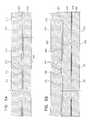
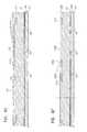
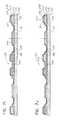
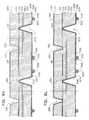
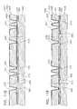
- FIGS. 1A-1Lare simplified sectional illustrations of a method for manufacturing packaged semiconductor chips in accordance with a preferred embodiment of the present invention
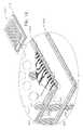
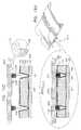
- FIG. 1Mis a simplified, partially cut away pictorial illustration of part of a packaged semiconductor chip manufactured in accordance with the method of FIGS. 1A-1L ;
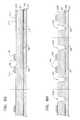
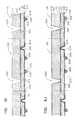
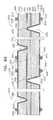
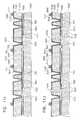
- FIGS. 2A-2Iare simplified illustrations of a method for manufacturing packaged semiconductor chips in accordance with another preferred embodiment of the present invention.
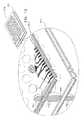
- FIG. 2Jis a simplified partially cut away pictorial illustration of part of a packaged semiconductor chip manufactured in accordance with the method of FIGS. 1A-1G and 2 A- 2 I;
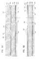
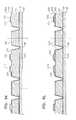
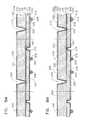
- FIGS. 3A-3Iare simplified sectional illustrations of a method for manufacturing packaged semiconductor chips in accordance with yet another preferred embodiment of the present invention.
- FIG. 3Jis a simplified partially pictorial, partially sectional illustration of part of a packaged semiconductor chip manufactured in accordance with the method of FIGS. 3A-3I ;
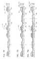
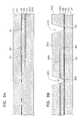
- FIGS. 4A-4Nare simplified sectional illustrations of a method for manufacturing packaged semiconductor chips in accordance with still another preferred embodiment of the present invention.
- FIG. 4Ois a simplified partially cut away pictorial illustration of part of a packaged semiconductor chip manufactured in accordance with the method of FIGS. 4A-4N ;
- FIGS. 5A-5Nare simplified sectional illustrations of a further method for manufacturing packaged semiconductor chips in accordance with a further preferred embodiment of the present invention.
- FIG. 5Ois a simplified partially cut away pictorial illustration of part of a packaged semiconductor chip manufactured in accordance with the method of FIGS. 5A-5N ;
- FIGS. 6A-6Pare simplified sectional illustrations of yet a further method for manufacturing packaged semiconductor chips in accordance with yet a further preferred embodiment of the present invention.
- FIG. 6Qis a simplified partially cut away pictorial illustration of part of a packaged semiconductor chip manufactured in accordance with the method of FIGS. 6A-6P ;
- FIGS. 7A-7Lare simplified sectional illustrations of still a further method for manufacturing packaged semiconductor chips in accordance with still a further preferred embodiment of the present invention.
- FIG. 7Mis a simplified partially cut away pictorial illustration of part of a packaged semiconductor chip manufactured in accordance with the method of FIGS. 7A-7L ;
- FIGS. 8A-8Pare simplified sectional illustrations of another method for manufacturing packaged semiconductor chips in accordance with another preferred embodiment of the present invention.
- FIG. 8Qis a simplified, partially cut away part-pictorial and part-sectional illustration of part of a packaged semiconductor chip manufactured in accordance with the method of FIGS. 8A-8P ;
- FIGS. 9A-9Qare simplified sectional illustrations of yet another method for manufacturing packaged semiconductor chips in accordance with another preferred embodiment of the present invention.
- FIG. 9Ris a simplified partially cut away part-pictorial and part-sectional illustration of part of a packaged semiconductor chip manufactured in accordance with the method of FIGS. 9A-9Q ;
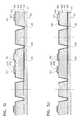
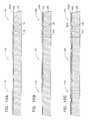
- FIGS. 10A-10Nare simplified sectional illustrations of still another method for manufacturing packaged semiconductor chips in accordance with another preferred embodiment of the present invention.
- FIG. 10Ois a simplified pictorial illustration of part of a packaged semiconductor chip manufactured in accordance with the method of FIGS. 10A-10N ;
- FIGS. 11A-11Jare simplified sectional illustrations of a method for manufacturing packaged stacked semiconductor chips in accordance with a further preferred embodiment of the present invention.
- FIG. 11Kis a simplified pictorial illustration of part of a packaged stacked semiconductor chip manufactured in accordance with the method of FIGS. 11A-11J ;
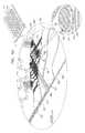
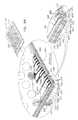
- FIG. 12is a simplified pictorial illustration of a packaged stacked semiconductor chip including semiconductor chips manufactured in accordance with the method of FIGS. 8A-8P ;
- FIG. 13is a simplified pictorial illustration of a packaged stacked semiconductor chip including semiconductor chips manufactured in accordance with the method of FIGS. 9A-9Q ;
- FIG. 14is a simplified partially sectional illustration of a packaged semiconductor chip constructed and operative in accordance with an additional preferred embodiment of the present invention.
- FIGS. 15A-15Dare simplified sectional illustrations of an additional method for manufacturing and mounting packaged semiconductor chips in accordance with a further preferred embodiment of the present invention.
- FIGS. 16A and 16Bare simplified sectional illustrations of a further method for manufacturing and mounting packaged semiconductor chips in accordance with yet a further preferred embodiment of the present invention.
- FIGS. 17A and 17Bare simplified illustrations of a method for manufacturing and mounting stacked packaged semiconductor chips in accordance with still another preferred embodiment of the present invention.
- FIGS. 18A-18Lare simplified sectional illustrations of yet a further method for manufacturing packaged semiconductor chips in accordance with yet a further preferred embodiment of the present invention.
- FIG. 18Mis a simplified partially cut away pictorial illustration of part of a packaged semiconductor chip manufactured in accordance with the method of FIGS. 18A-18L .
- FIGS. 1A-1Lare simplified sectional illustrations of a method for manufacturing packaged semiconductor chips in accordance with a preferred embodiment of the present invention.
- FIG. 1Athere is seen part of a semiconductor wafer 100 including dies 102 , each typically having an active surface 104 including electrical circuitry 106 having bond pads 108 .
- the wafer 100is typically silicon of thickness 730 microns.
- the electrical circuitry 106may be provided by any suitable conventional technique.
- the wafer 100may be any other suitable material, such as, for example, Gallium Arsenide and may be of any suitable thickness.
- FIG. 1Bshows a wafer-scale packaging layer 110 attached to wafer 100 by an adhesive 112 , such as epoxy.
- the adhesive 112covers the active surfaces 104 of dies 102 .
- the adhesiveis homogeneously applied to the packaging layer by spin bonding, as described in U.S. Pat. Nos. 5,980,663 and 6,646,289, the contents of which is hereby incorporated by reference. Alternatively, any other suitable technique may be employed.
- the forming a packaging layerincludes a forming a packaging layer of a material having thermal expansion characteristics similar to those of the semiconductor wafer.
- the forming a packaging layerincludes forming a packaging layer of silicon.
- the placing compliant materialincludes placing silicone.
- the semiconductor wafer 100is thinned as by machining its non-active surface 114 .
- the thickness of the semiconductor wafer 100 at this stage, following thinning thereof,is 300 microns.
- FIG. 1Dshows notches 120 , preferably formed by photolithography employing plasma etching or wet etching techniques, at locations which overlie bond pads 108 .
- the notches 120preferably do not extend through adhesive 112 .
- FIG. 1Eit is seen that the adhesive 112 overlying bond pads 108 and underlying notches 120 is removed, preferably by dry etching.
- FIG. 1Fshows the formation of an electrophoretic, electrically insulative compliant layer 122 over the packaging layer 110 .
- suitable compliant layersinclude Powercron 645 and Powercron 648, both commercially available from PPG of Pittsburgh, Pa., USA; Cathoguard 325, commercially available from BASF of Southfield, Mass., USA; Electrolac, commercially available from Macdermid of Waterbury, Conn., USA and Lectraseal DV494 and Lectrobase 101, both commercially available from LVH Coatings of Birmingham, UK.
- compliant layer 122encapsulates all exposed surfaces of the packaging layer 110 .
- Compliant layer 122preferably provides protection to the device from alpha particles emitted by BGA solder balls.
- FIG. 1Gillustrates the formation of a metal layer 130 , by sputtering chrome, aluminum or copper.
- Metal layer 130extends from the bond pads 108 , over the compliant layer 122 and along the inclined surfaces of the packaging layer 110 , defined by notches 120 , onto outer, generally planar surfaces of the compliant layer 122 at dies 102 .
- metal connections 132are preferably formed by patterning the metal layer 130 , preferably by 3D photolithography employing a suitable photoresist, preferably Eagle 2100, commercially available from Rohm and Haas Shipley Division of Marlborough, Mass., U.S.A.
- a suitable photoresistpreferably Eagle 2100, commercially available from Rohm and Haas Shipley Division of Marlborough, Mass., U.S.A.
- the metal connections 132may be plated with nickel, as by electroless techniques, in order to provide enhanced corrosion resistance.
- FIG. 1Iillustrates the application, preferably by spray coating, of a second, electrically insulative, encapsulant passivation layer 134 over the metal connections 132 and over the compliant layer 122 .
- encapsulant passivation layer 134comprises solder mask.
- FIG. 1Jshows patterning of the encapsulant passivation layer 134 , preferably by photolithography, to define solder bump locations 135 .
- FIG. 1Killustrates the formation of solder bumps 140 at locations 135 on the metal connections 132 , at which the encapsulant passivation layer 134 is not present.
- FIG. 1Lshows dicing of the wafer 100 and packaging layer 110 of FIG. 1K along scribe lines 142 to produce a multiplicity of individually packaged dies 144 .
- FIG. 1Mis a simplified, partially cut away pictorial illustration of part of a packaged semiconductor DRAM chip manufactured in accordance with the method of FIGS. 1A-1L .
- a notch 150corresponding to notch 120 ( FIGS. 1D-1L )
- a packaging layer 152corresponding to packaging layer 110 ( FIGS. 1B-1L )
- FIGS. 1B-1Lforms part of a die 153 , corresponding to die 144 ( FIG. 1L ).
- the notch 150exposes a row of bond pads 154 , corresponding to bond pads 108 ( FIGS. 1A-1L ).
- a layer 156 of adhesive, corresponding to layer 112 ( FIGS. 1B-1L )covers a silicon layer 158 , corresponding to semiconductor wafer 100 , of the silicon wafer die 153 other than at notch 150 , and packaging layer 152 covers the adhesive 156 .
- An electrophoretic, electrically insulative compliant layer 160covers the packaging layer 152 and extends along inclined surfaces of notch 150 , but does not cover the bond pads 154 .
- Patterned metal connections 162corresponding to metal connections 132 ( FIGS. 1H-1L ), extend from bond pads 154 along the inclined surfaces of notch 150 and over generally planar surfaces of compliant layer 160 to solder bump locations 164 , corresponding to solder bump locations 135 ( FIGS. 1J-1L ).
- An encapsulant passivation layer 166corresponding to encapsulant passivation layer 134 ( FIGS. 1I-1L ), is formed over compliant layer 160 and metal connections 162 other than at locations 164 .
- Solder bumps 168corresponding to solder bumps 140 ( FIGS. 1K and 1L ), are formed onto metal connections 162 at locations 164 .
- FIGS. 2A-2Iillustrate an alternative methodology, useful for some of the bond pads 108 .
- the methodology of FIGS. 2A-2Itakes place following the steps of FIGS. 1A-1G , and replaces steps 1 H, 1 I, 1 J, 1 K and 1 L.
- the methodology of FIGS. 1A-1G and 2 A- 2 Iis particularly useful for devices having a high density of bond pads 108 , such as DRAMs.
- FIG. 2Aillustrates patterning of metal layer 130 ( FIG. 1G ) to define metal connections 252 , preferably by 3D photolithography employing a suitable photoresist, preferably Eagle 2100, commercially available from Rohm and Haas Shipley Division of Marlborough, Mass., U.S.A.
- a suitable photoresistpreferably Eagle 2100, commercially available from Rohm and Haas Shipley Division of Marlborough, Mass., U.S.A.
- the metal connections 252may be plated with nickel, as by electroless techniques, in order to provide enhanced corrosion resistance.
- FIG. 2Bshows the application, preferably by spray coating, of a second, electrically insulative, encapsulant passivation layer 254 over the metal connections 252 and over the compliant layer 122 .
- the encapsulant passivation layer 254comprises solder mask.
- FIG. 2Cshows patterning of the encapsulant passivation layer 254 , preferably by photolithography.
- FIG. 2Dillustrates the formation of a second metal layer 260 by sputtering chrome, aluminum or copper.
- Metal layer 260extends from the metal connections 252 over the encapsulant passivation layer 254 .
- metal connections 262are preferably formed by patterning metal layer 260 , preferably by 3D photolithography employing a suitable photoresist, preferably Eagle 2100, commercially available from Rohm and Haas Shipley Division of Marlborough, Mass., U.S.A.
- a suitable photoresistpreferably Eagle 2100, commercially available from Rohm and Haas Shipley Division of Marlborough, Mass., U.S.A.
- the metal connections 262may be plated with nickel, as by electroless techniques, in order to provide enhanced corrosion resistance.
- FIG. 2Fshows the application, preferably by spray coating, of a third, electrically insulative, encapsulant passivation layer 264 over the metal connections 262 and over the encapsulant passivation layer 254 and the compliant layer 122 .
- the encapsulant passivation layer 264comprises solder mask.
- FIG. 2Gshows patterning of the encapsulant passivation layer 264 , preferably by photolithography, to define solder bump locations 266 .
- FIG. 2Hillustrates the formation of solder bumps 270 at solder bump locations 266 , at which the encapsulant passivation layer 264 is not present.
- FIG. 2Ishows dicing of the wafer 100 and packaging layer 110 of FIG. 2H along scribe lines 272 to produce a multiplicity of individually packaged dies 274 .
- FIG. 2Jis a simplified partially cut away pictorial illustration of part of a packaged semiconductor DRAM chip manufactured in accordance with the method of FIGS. 1A-1G and 2 A- 2 I.
- a notch 276corresponding to notch 120 ( FIGS. 2A-2I ) is formed in packaging layer 277 , corresponding to packaging layer 110 ( FIGS. 2A-2H ), which forms part of a silicon wafer die 278 , corresponding to die 274 ( FIG. 2I ).
- the notch 276exposes a row of bond pads 279 , corresponding to bond pads 108 ( FIGS. 2A-2I ).
- a layer 280 of adhesivecorresponding to layer 112 ( FIGS. 2A-2I ), covers a silicon layer 282 , corresponding to semiconductor wafer 100 , of silicon wafer die 278 other than at notch 276 and packaging layer 277 covers the adhesive 280 .
- An electrophoretic, electrically insulative compliant layer 284covers the packaging layer 277 and extends along inclined surfaces of notch 276 , but does not cover the bond pads 279 .
- Patterned metal connections 286corresponding to metal connections 132 ( FIGS. 1H-1L ), extend from some of bond pads 279 along the inclined surfaces of notch 276 and over generally planar surfaces of compliant layer 284 to solder bump locations 288 , corresponding to some of solder bump locations 135 ( FIGS. 1J-1L ).
- Other patterned metal connections 286corresponding to metal connections 252 ( FIGS. 2A-2I ), extend from other bond pads 279 along the inclined surfaces of notch 276 to additional locations 290 .
- An encapsulant passivation layer 292corresponding to encapsulant passivation layer 254 ( FIGS. 2B-2I ), is formed over compliant layer 284 and metal connections 286 other than at solder bump locations 288 and additional locations 290 .
- Additional metal connections 294corresponding to metal connections 262 ( FIGS. 2E-2I ), extend from additional locations 290 over generally planar surfaces of compliant layer 284 to solder bump locations 296 , corresponding to solder bump locations 266 ( FIGS. 2G-2I ).
- Solder bumps 298corresponding to solder bumps 270 ( FIGS. 2H and 2I ) are formed onto metal connections 294 at locations 296 .
- An encapsulant passivation layer 299corresponding to encapsulant passivation layer 264 ( FIGS. 2G-2I ), is formed over encapsulant passivation layer 292 and metal connections 294 other than at solder bump locations 296 .
- FIGS. 3A-3Iare simplified sectional illustrations of a method for manufacturing packaged semiconductor chips in accordance with yet another preferred embodiment of the present invention wherein the packaging layer 110 is electrically conductive.
- the method of FIGS. 3A-3Iemploys the steps described hereinabove with reference to FIGS. 1A-1C , which are followed by the steps shown in FIGS. 3A-3I .
- FIG. 3Ashows notches 300 and 302 formed in the structure of FIG. 1C , described hereinabove.
- Notches 300 and 302are preferably formed by photolithography, employing plasma etching or wet etching techniques, and preferably do not extend through adhesive 112 .
- Notches 300are formed at locations which overlie bond pads 108 and are similar to notches 120 of FIGS. 1D-1L and 2 A- 2 I.
- notches 302are wider than notches 300 and are symmetrically formed on both sides of scribe lines 304 .
- Notches 302are of varying width and depth, such that at corners of dies at which adjacent dies meet, there is provided electrically conductive continuity of the packaging layer 110 across adjacent dies 102 prior to dicing. This is achieved by decreasing the depth and corresponding width of the notches 302 at junctions of adjacent dies 102 .
- FIG. 3Bit is seen that the adhesive 112 overlying bond pads 108 and underlying notches 300 is removed, preferably by dry etching.
- FIG. 3Cshows the formation of an electrophoretic, electrically insulative compliant layer 322 over the packaging layer 110 .
- suitable materials for compliant layer 322are those described hereinabove with reference to FIG. 1F .
- compliant layer 322encapsulates all exposed surfaces of the packaging layer 110 .
- Compliant layer 322preferably provides protection to the device from alpha particles emitted by BGA solder balls.
- FIG. 3Dillustrates the formation of a metal layer 330 , by sputtering chrome, aluminum or copper.
- Metal layer 330extends from the bond pads 108 , over the compliant layer 322 and along the inclined surfaces of the packaging layer 110 , defined by notches 300 and 302 , onto outer, generally planar surfaces of the compliant layer 322 at dies 102 .
- metal connections 332are preferably formed by patterning the metal layer 330 , preferably by 3D photolithography employing a suitable photoresist, preferably Eagle 2100, commercially available from Rohm and Haas Shipley Division of Marlborough, Mass., U.S.A.
- a suitable photoresistpreferably Eagle 2100, commercially available from Rohm and Haas Shipley Division of Marlborough, Mass., U.S.A.
- the metal connections 332may be plated with nickel, as by electroless techniques, in order to provide enhanced corrosion resistance.
- FIG. 3Fillustrates the application, preferably by spray coating, of a second, electrically insulative, encapsulant passivation layer 334 over the metal connections 332 and over the compliant layer 322 .
- the encapsulant passivation layer 334comprises solder mask.
- FIG. 3Gshows patterning of the encapsulant passivation layer 334 , preferably by photolithography, to define solder bump locations 336 .
- FIG. 3Hillustrates the formation of solder bumps 340 at locations 336 on the metal connections 332 , at which the encapsulant passivation layer 334 is not present.
- FIG. 3Ishows dicing of the wafer 100 and packaging layer 110 of FIG. 3H along scribe lines 304 to produce a multiplicity of individually packaged dies 344 having inclined surfaces 346 adjacent the scribe lines 304 .
- each individually package die 344includes a straight-edged base portion 350 including an edge defined by a silicon layer 352 , corresponding to a portion of semiconductor wafer 100 ( FIGS. 3A-3I ) overlaid with a layer 354 of adhesive, corresponding to adhesive layer 112 ( FIGS. 3A-3I ).
- an inclined edge portion 358Disposed over straight-edged base portion 350 and set back slightly therefrom, other than at the corners of the packaged semiconductor DRAM chip, thereby defining a shoulder 356 , is an inclined edge portion 358 corresponding to inclined surface 346 ( FIG. 3I ). Since the depth and corresponding width of the notches 302 are decreased at junctions of adjacent dies 102 , shoulders 356 do not extend to the corners.
- the inclined edge portion 358is defined by an encapsulant passivation layer 360 , corresponding to encapsulant passivation layer 334 ( FIGS. 3F-3I ) which overlies an electrophoretic, electrically insulative compliant layer 362 , corresponding to electrophoretic, electrically insulative compliant layer 322 ( FIG. 3B-3I ), which in turn overlies a packaging layer 364 , corresponding to packaging layer 110 ( FIGS. 3A-3I ).
- each individually package die 344includes a straight-edged corner portion 370 including a corner defined by silicon layer 352 , overlaid with layer 354 of adhesive, above which is a portion of packaging layer 364 , electrophoretic, electrically insulative compliant layer 362 and encapsulant passivation layer 360 .
- FIGS. 4A-4Nare simplified sectional illustrations of a method for manufacturing packaged semiconductor chips in accordance with still another preferred embodiment of the present invention.
- FIG. 4Athere is seen part of a semiconductor wafer 500 .
- the wafer 500is typically formed of silicon and has a thickness of 730 microns.
- the wafer 500may be formed of any other suitable material and may be of any suitable thickness.
- FIG. 4Bshows the formation of a plurality of recesses 502 in a surface 504 of wafer 500 as by a conventional etching technique.
- FIG. 4Cshows filling of the recesses 502 with a compliant material 506 , preferably a silicone-based material such as Dow WL-5150, commercially available from Dow Corning, Inc., typically by use of a squeegee.
- the compliant material 506is then cured in a conventional manner.
- FIG. 4Dshows removal of excess compliant material 506 and planarization of surface 504 , as by grinding, thereby leaving platforms 507 of compliant material 506 in recesses 502 .
- FIG. 4Eshows the application of an adhesive 508 onto surface 504 , overlying recesses 502 filled with compliant material 506 defining platforms 507 , as by spin coating.
- Adhesive 508is preferably a suitable epoxy.
- FIG. 4Fshows the wafer 500 of FIG. 4E , turned upside down and bonded onto the structure of FIG. 1F , described hereinabove, and here designated by reference numeral 510 , with a surface 512 , opposite surface 504 being exposed.
- FIG. 4Gshows thinning of wafer 500 , preferably by grinding surface 512 , down to a thickness equal to the depth of recesses 502 , typically 100 microns.
- FIG. 4Hshows removal of the remainder of wafer 500 , and those portions of adhesive 508 not underlying platforms 507 of compliant material 506 , as by silicon etching and ultrasonic cleaning.
- FIG. 4Iillustrates the formation of a metal layer 514 , by sputtering chrome, aluminum or copper.
- Metal layer 514extends from the bond pads 108 , over the compliant layer 122 and along the inclined surfaces of the packaging layer 110 , defined by notches 120 , onto outer, generally planar surfaces of the compliant layer 122 and over platforms 507 at dies 102 .
- metal connections 516are preferably formed by patterning the metal layer 514 , preferably by 3D photolithography employing a suitable photoresist, preferably Eagle 2100, commercially available from Rohm and Haas Shipley Division of Marlborough, Mass., U.S.A.
- a suitable photoresistpreferably Eagle 2100, commercially available from Rohm and Haas Shipley Division of Marlborough, Mass., U.S.A.
- the metal connections 516may be plated with nickel, as by electroless techniques, in order to provide enhanced corrosion resistance.
- FIG. 4Killustrates the application, preferably by spray coating, of a second, electrically insulative, encapsulant passivation layer 518 over the metal connections 516 , over the compliant layer 122 and over platforms 507 .
- the encapsulant passivation layer 518comprises solder mask.
- FIG. 4Lshows patterning of the encapsulant passivation layer 518 , preferably by photolithography, to define solder bump locations 519 .
- FIG. 4Millustrates the formation of solder bumps 520 onto platforms 507 at locations on the metal connections 516 at which the encapsulant passivation layer 518 is not present.
- FIG. 4Nshows dicing of the wafer 100 and packaging layer 110 of FIG. 4M along scribe lines 522 to produce a multiplicity of individually packaged dies 524 .
- FIG. 4Ois a simplified partially cut away pictorial illustration of part of a packaged semiconductor DRAM chip manufactured in accordance with the method of FIGS. 4A-4N .
- a notch 550corresponding to notch 120 ( FIGS. 4F-4N ), is formed in a packaging layer 551 of a silicon wafer die 552 , corresponding to die 524 ( FIG. 4N ).
- the notch 550exposes a row of bond pads 554 , corresponding to bond pads 108 ( FIGS. 4F-4N ).
- a layer 556 of adhesive, corresponding to layer 112 ( FIGS. 4F-4N )covers a silicon layer 558 , corresponding to semiconductor wafer 100 , the silicon wafer die 552 other than at notch 550 and packaging layer 551 covers the adhesive 556 .
- An electrophoretic, electrically insulative compliant layer 560covers the packaging layer 551 and extends along inclined surfaces of notch 550 , but does not cover the bond pads 554 .
- Platforms 562corresponding to platforms 507 ( FIGS. 4D-4N ) are formed over compliant layer 560 at solder bump locations 564 , corresponding to solder bump locations 519 ( FIGS. 4L-4N ).
- Patterned metal connections 566corresponding to metal connections 516 ( FIGS. 4J-4N ), extend from bond pads 554 along the inclined surfaces of notch 550 and over generally planar surfaces of compliant layer 560 and terminate over platforms 562 .
- An encapsulant passivation layer 568corresponding to encapsulant passivation layer 518 (FIGS. 4 K- 4 N), is formed over compliant layer 560 and metal connections 562 other than at locations 564 .
- Solder bumps 570corresponding to solder bumps 520 ( FIGS. 4M and 4N ), are formed onto metal connections 566 at locations 564 .
- FIGS. 5A-5Nare simplified sectional illustrations of a further method for manufacturing packaged semiconductor chips in accordance with a further preferred embodiment of the present invention.
- FIGS. 5A-5Nemploys the steps described hereinabove with reference to FIGS. 4A-4E , which are followed by the steps shown in FIGS. 5A-5N .
- FIG. 5Ashows the wafer 500 of FIG. 4E , turned upside down and bonded onto a wafer scale packaging layer 900 , preferably a silicon wafer, with a surface 902 of packaging layer 900 being exposed.
- a wafer scale packaging layer 900preferably a silicon wafer
- FIG. 5Bshows the structure of FIG. 5A bonded at surface 902 to the structure of FIG. 1A at surface 104 thereof, preferably by means of an adhesive 904 , such as epoxy.
- FIG. 5Cshows thinning of wafer 100 , preferably by machining its non-active surface 114 .
- the thickness of the semiconductor wafer 100 at this stage, following thinning thereof,is 300 microns.
- FIG. 5Dshows thinning of wafer 500 , preferably by grinding surface 512 , down to a thickness equal to the depth of recesses 502 , typically 100 microns.
- FIG. 5Eshows removal of the remainder of wafer 500 , and those portions of adhesive 508 not underlying platforms 507 of compliant material 506 , as by silicon etching and ultrasonic cleaning.
- FIG. 5Fshows notches 920 , preferably formed by photolithography employing plasma etching or wet etching techniques, at locations which overlie bond pads 108 .
- the notchespreferably do not extend through adhesive 904 .
- FIG. 5Git is seen that the adhesive 904 overlying bond pads 108 and underlying notches 920 is removed, preferably by dry etching.
- FIG. 5Hshows the formation of an electrophoretic, electrically insulative compliant layer 922 over those portions of packaging layer 900 not underlying platforms 507 .
- suitable materials for compliant layer 922are those described hereinabove with reference to FIG. 1F .
- compliant layer 922encapsulates all exposed surfaces of the packaging layer 900 .
- Compliant layer 922preferably provides protection to the device from alpha particles emitted by BGA solder balls.
- FIG. 5Iillustrates the formation of a metal layer 924 , by sputtering chrome, aluminum or copper.
- Metal layer 924extends from the bond pads 108 , over the compliant layer 922 and along the inclined surfaces of the packaging layer 900 , defined by notches 920 , onto outer, generally planar surfaces of the compliant layer 922 and over platforms 507 at dies 102 .
- metal connections 926are preferably formed by patterning the metal layer 924 , preferably by 3D photolithography employing a suitable photoresist, preferably Eagle 2100, commercially available from Rohm and Haas Shipley Division of Marlborough, Mass., U.S.A.
- a suitable photoresistpreferably Eagle 2100, commercially available from Rohm and Haas Shipley Division of Marlborough, Mass., U.S.A.
- the metal connections 926may be plated with nickel, as by electroless techniques, in order to provide enhanced corrosion resistance.
- FIG. 5Killustrates the application, preferably by spray coating, of a second, electrically insulative, encapsulant passivation layer 930 over the metal connections 926 , over the compliant layer 922 and over platforms 507 .
- the encapsulant passivation layer 930comprises solder mask.
- FIG. 5Lshows patterning of the encapsulant passivation layer 930 , preferably by photolithography, to define solder bump locations 931 .
- FIG. 5Millustrates the formation of solder bumps 932 onto platforms 507 at locations 931 on the metal connections 926 , at which the encapsulant passivation layer 930 is not present.
- FIG. 5Nshows dicing of the wafer 100 and packaging layer 110 of FIG. 5M along scribe lines 942 to produce a multiplicity of individually packaged dies 944 .
- FIG. 5Ois a simplified partially cut away pictorial illustration of part of a packaged semiconductor DRAM chip manufactured in accordance with the method of FIGS. 5A-5N .
- a notch 950corresponding to notch 920 ( FIGS. 5F-5N ) is formed in a packaging layer 951 , corresponding to packaging layer 900 ( FIGS. 5A-5N ), of silicon wafer die 952 , corresponding to die 944 ( FIG. 5N ).
- the notch 950exposes a row of bond pads 954 , corresponding to bond pads 108 ( FIGS. 5B-5N ).
- a layer 956 of adhesive, corresponding to layer 904 ( FIGS. 5B-5N )covers a silicon layer 958 , corresponding to semiconductor wafer 100 , of the silicon wafer die 952 other than at notch 950 and packaging layer 951 covers the adhesive 956 .
- Platforms 960corresponding to platforms 507 ( FIGS. 5A-5N ) are formed over packaging layer 951 at solder bump locations 961 , corresponding to solder bump locations 931 ( FIGS. 5L-5N ).
- An electrophoretic, electrically insulative compliant layer 962covers the packaging layer 951 , surrounds platforms 960 and extends along inclined surfaces of notch 950 , but does not cover the bond pads 954 .
- Patterned metal connections 966corresponding to metal connections 926 ( FIGS. 5J-5N ), extend from bond pads 954 along the inclined surfaces of notch 950 and over generally planar surfaces of compliant layer 962 and terminate over platforms 960 .
- An encapsulant passivation layer 968corresponding to encapsulant passivation layer 930 ( FIGS. 5K-5N ), is formed over compliant layer 962 and metal connections 966 other than at locations 961 .
- Solder bumps 970corresponding to solder bumps 932 ( FIGS. 5M and 5N ), are formed onto metal connections 966 at locations 961 .
- FIGS. 6A-6Pare simplified sectional illustrations of yet a further method for manufacturing packaged semiconductor chips in accordance with yet a further preferred embodiment of the present invention.
- FIGS. 6A-6Pemploys the steps described hereinabove with reference to FIGS. 1A-1C , which are followed by the steps shown in FIGS. 6A-6P .
- FIG. 6Ashows a structure similar to the structure of FIG. 1C , but having a packaging layer 1300 which is thicker than packaging layer 110 ( FIG. 1C ).
- a packaging layer 1300which is thicker than packaging layer 110 ( FIG. 1C ).
- surface 1302undergoes electrophoretic deposition of a layer of photoresist 1306 , followed by lithography, which leaves portions 1308 of the bottom surfaces 1310 of recesses 1304 exposed to etching, as seen in FIG. 6C .
- Subsequent silicon etchingproduces an undercut recess 1312 at each recess 1304 , as seen in FIG. 6D .
- FIG. 6Eshows filling of the recesses 1312 and 1304 with a compliant material 1314 , preferably a silicone-based material such as Dow WL-5150, commercially available from Dow Corning, Inc., typically by use of a squeegee.
- a compliant material 1314preferably a silicone-based material such as Dow WL-5150, commercially available from Dow Corning, Inc., typically by use of a squeegee.
- the compliant material 1314is then cured in a conventional manner.
- FIG. 6Fshows removal of excess compliant material 1314 and planarization of surface 1302 , as by grinding, thereby leaving platforms 1316 of compliant material 1314 in recesses 1312 and 1304 .
- FIG. 6Gshows removal of the portions of packaging layer 1300 surrounding but not underlying platforms 1316 of compliant material 1314 , as by silicon etching and ultrasonic cleaning.
- FIG. 6Hshows notches 1320 , preferably formed by photolithography employing plasma etching or wet etching techniques, at locations which overlie bond pads 108 .
- the notchespreferably do not extend through adhesive 112 .
- FIG. 6Iit is seen that the adhesive 112 overlying bond pads 108 and underlying notches 1320 is removed, preferably by dry etching.
- FIG. 6Jshows the formation of an electrophoretic, electrically insulative compliant layer 1322 over those portions of packaging layer 1300 not underlying platforms 1316 .
- suitable materials for compliant layer 1322are those described hereinabove with reference to FIG. 1F .
- compliant layer 1322encapsulates all exposed surfaces of the packaging layer 1300 .
- Compliant layer 1322preferably provides protection to the device from alpha particles emitted by BGA solder balls.
- FIG. 6Killustrates the formation of a metal layer 1324 , by sputtering chrome, aluminum or copper.
- Metal layer 1324extends from the bond pads 108 , over the compliant layer 1322 and along the inclined surfaces of the packaging layer 1300 , defined by notches 1320 , onto outer, generally planar surfaces of the compliant layer 1322 and over platforms 1316 at dies 102 .
- metal connections 1326are preferably formed by patterning the metal layer 1324 , preferably by 3D photolithography employing a suitable photoresist, preferably Eagle 2100, commercially available from Rohm and Haas Shipley Division of Marlborough, Mass., U.S.A.
- a suitable photoresistpreferably Eagle 2100, commercially available from Rohm and Haas Shipley Division of Marlborough, Mass., U.S.A.
- the metal connections 1326may be plated with nickel, as by electroless techniques, in order to provide enhanced corrosion resistance.
- FIG. 6Millustrates the application, preferably by spray coating, of a second, electrically insulative, encapsulant passivation layer 1330 over the metal connections 1326 , over the compliant layer 1322 and over platforms 1316 .
- the encapsulant passivation layer 1330comprises solder mask.
- FIG. 6Nshows patterning of the encapsulant passivation layer 1330 , preferably by photolithography, to define solder bump locations 1331 .
- FIG. 6Oillustrates the formation of solder bumps 1332 onto platforms 1316 at locations 1331 on the metal connections 1326 at which the encapsulant passivation layer 1330 is not present.
- FIG. 6Pshows dicing of the wafer 100 and packaging layer 1300 of FIG. 6O along scribe lines 1342 to produce a multiplicity of individually packaged dies 1344 .
- FIG. 6Qis a simplified partially cut away pictorial illustration of part of a packaged semiconductor DRAM chip manufactured in accordance with the method of FIGS. 6A-6P .
- a notch 1350corresponding to notch 1320 ( FIGS. 6H-6P ) is formed in a packaging layer 1351 , corresponding to packaging layer 1300 ( FIGS. 6A-6P ), of a silicon wafer die 1352 , corresponding to die 1344 ( FIG. 6P ).
- the notch 1350exposes a row of bond pads 1354 , corresponding to bond pads 108 ( FIGS. 6A-6P ).
- a layer 1356 of adhesivecorresponding to layer 112 ( FIGS. 6A-6P ), covers a silicon layer 1358 , corresponding to semiconductor wafer 100 ( FIGS. 6A-6P ), of the silicon wafer die 1352 other than at notch 1350 and packaging layer 1351 covers the adhesive 1356 .
- Platforms 1360corresponding to platforms 1316 ( FIGS. 6F-6P ) are formed over packaging layer 1351 at solder bump locations 1361 , corresponding to solder bump locations 1331 ( FIGS. 6N-6P ). It is a particular feature of the embodiment of FIGS. 6A-6Q that platforms 1360 are formed directly onto the packaging layer 1351 and not, as in the embodiment of FIGS. 5A-5O , formed over a layer of adhesive.
- An electrophoretic, electrically insulative compliant layer 1362covers the packaging layer 1351 , surrounds platforms 1360 and extends along inclined surfaces of notch 1350 , but does not cover the bond pads 1354 .
- Patterned metal connections 1366corresponding to metal connections 1326 ( FIGS. 6L-6P ), extend from bond pads 1354 along the inclined surfaces of notch 1350 and over generally planar surfaces of compliant layer 1362 and terminate over platforms 1360 .
- An encapsulant passivation layer 1368corresponding to encapsulant passivation layer 1330 ( FIGS. 6M-6P ), is formed over compliant layer 1362 and metal connections 1366 other than at locations 1361 .
- Solder bumps 1370corresponding to solder bumps 1332 ( FIGS. 6O and 6P ), are formed onto metal connections 1366 at locations 1361 .
- FIGS. 7A-7Lare simplified sectional illustrations of still a further method for manufacturing packaged semiconductor chips in accordance with still a further preferred embodiment of the present invention.
- FIGS. 7A-7Lemploys the steps described hereinabove with reference to FIGS. 4A-4E , which are preceded by the steps shown in FIGS. 7A-7C and followed by the steps shown in FIGS. 7D-7L .
- FIG. 7Ashows the structure of FIG. 1A having formed thereover an encapsulant passivation layer 1700 , typically comprising a suitable polymer, such as, for example a polyimide, which provides protection to the device from alpha particles emitted by BGA solder balls.
- a suitable polymersuch as, for example a polyimide
- FIG. 7Bshows thinning of wafer 100 , preferably by machining its non-active surface 114 .
- the thickness of the semiconductor wafer 100 at this stage, following thinning thereofis 300 microns.
- FIG. 7Cshows the structure of FIG. 7B following patterning of the encapsulant passivation layer 1700 , by conventional etching methodology, to expose bond pads 108 on the active surface 104 of semiconductor wafer 100 .
- FIG. 7Dshows the wafer 500 of FIG. 4E , turned upside down and bonded onto the structure of FIG. 7C , with a surface 512 , opposite surface 504 being exposed.
- FIG. 7Eshows thinning of wafer 500 , preferably by grinding surface 512 , down to a thickness equal to the depth of recesses 502 , typically 100 microns.
- FIG. 7Fshows removal of the remainder of wafer 500 and those portions of adhesive 508 not underlying platforms 507 of compliant material 506 , as by silicon etching and ultrasonic cleaning.
- FIG. 7Gillustrates the formation of a metal layer 1714 , by sputtering chrome, aluminum or copper.
- Metal layer 1714extends from the bond pads 108 , along the inclined surfaces of encapsulant passivation layer 1700 , onto outer, generally planar surfaces of the encapsulant passivation layer 1700 and over platforms 507 at dies 102 .
- metal connections 1716are preferably formed by patterning the metal layer 1714 , preferably by 3D photolithography employing a suitable photoresist, preferably Eagle 2100, commercially available from Rohm and Haas Shipley Division of Marlborough, Mass., U.S.A.
- a suitable photoresistpreferably Eagle 2100, commercially available from Rohm and Haas Shipley Division of Marlborough, Mass., U.S.A.
- the metal connections 1716may be plated with nickel, as by electroless techniques, in order to provide enhanced corrosion resistance.
- FIG. 7Iillustrates the application, preferably by spray coating, of an electrically insulative, encapsulant passivation layer 1718 over the metal connections 1716 , over the encapsulant passivation layer 1700 and over platforms 507 .
- the encapsulant passivation layer 1718comprises solder mask.
- FIG. 7Jshows patterning of the encapsulant passivation layer 1718 , preferably by photolithography, to define solder bump locations 1719 .
- FIG. 7Killustrates the formation of solder bumps 1720 onto platforms 507 at locations 1719 on the metal connections 1716 at which the encapsulant passivation layer 1718 is not present.
- FIG. 7Lshows dicing of the wafer 100 and packaging layer of FIG. 7K along scribe lines 1722 to produce a multiplicity of individually packaged dies 1724 .
- FIG. 7Mis a simplified partially cut away pictorial illustration of part of a packaged semiconductor DRAM chip manufactured in accordance with the method of FIGS. 7A-7L .
- a notch 1740produced by patterning of an encapsulant passivation layer 1742 , corresponding to encapsulant passivation layer 1700 ( FIG. 7C ), of a silicon wafer die 1743 , corresponding to silicon wafer die 1724 ( FIG. 7L ), exposes a row of bond pads 1754 , corresponding to bond pads 108 ( FIGS. 7A-7L ).
- Platforms 1762corresponding to platforms 507 ( FIGS. 7F-7L ) are formed over encapsulant passivation layer 1742 at solder bump locations 1764 , corresponding to solder bump locations 1719 ( FIGS. 7J-7L ).
- Patterned metal connections 1766corresponding to metal connections 1716 ( FIGS. 7H-7L ), extend from bond pads 1754 along the inclined surfaces of notch 1740 and over generally planar surfaces of encapsulant passivation layer 1742 and terminate over platforms 1762 .
- An encapsulant passivation layer 1768corresponding to encapsulant passivation layer 1718 ( FIGS. 7I-7L ), is formed over encapsulant passivation layer 1742 and metal connections 1766 other than at locations 1764 .
- Solder bumps 1770corresponding to solder bumps 1720 ( FIGS. 7K and 7L ), are formed onto metal connections 1766 at locations 1764 .
- FIGS. 8A-8Pare simplified sectional illustrations of another method for manufacturing packaged semiconductor chips in accordance with another preferred embodiment of the present invention.
- the method of FIGS. 8A-8Pemploys the steps described hereinabove with reference to FIGS. 1A-1C , which are followed by the steps shown in FIGS. 8A-8P .
- FIG. 8Ashows the structure of FIG. 1C turned upside-down.
- Notches 2120preferably formed by photolithography employing plasma etching or wet etching techniques, are formed in semiconductor wafer 100 at locations which overlie, in the sense of FIG. 8A , some of bond pads 108 , here designated by reference numeral 2121 .
- FIG. 8Bshows the formation of an electrophoretic, electrically insulative compliant layer 2122 over the semiconductor wafer 100 .
- suitable materials for compliant layer 2122are those described hereinabove with reference to FIG. 1F .
- compliant layer 2122encapsulates all exposed surfaces of the semiconductor wafer 100 .
- Compliant layer 2122preferably provides protection to the device from alpha particles emitted by BGA solder balls.
- FIG. 8Cillustrates the formation of a metal layer 2130 , by sputtering chrome, aluminum or copper.
- Metal layer 2130extends from the bond pads 2121 , over the compliant layer 2122 and along the inclined surfaces of the semiconductor wafer 100 , defined by notches 2120 onto outer, generally planar surfaces of the compliant layer 2122 .
- metal connections 2132are preferably formed by patterning the metal layer 2130 , preferably by 3D photolithography employing a suitable photoresist, preferably Eagle 2100, commercially available from Rohm and Haas Shipley Division of Marlborough, Mass., U.S.A.
- a suitable photoresistpreferably Eagle 2100, commercially available from Rohm and Haas Shipley Division of Marlborough, Mass., U.S.A.
- the metal connections 2132may be plated with nickel, as by electroless techniques, in order to provide enhanced corrosion resistance.
- FIG. 8Eillustrates the application, preferably by spray coating, of a second, electrically insulative, encapsulant passivation layer 2134 over the metal connections 2132 and over the compliant layer 2122 .
- the encapsulant passivation layer 2134comprises solder mask.
- FIG. 8Fshows patterning of the encapsulant passivation layer 2134 , preferably by photolithography, to define solder bump locations 2136 .
- FIG. 8Gillustrates the formation of solder bumps 2140 at locations 2136 on the metal connections 2132 , at which the encapsulant passivation layer 2134 is not present.
- FIG. 8Hshows the structure of FIG. 8G turned upside-down.
- Notches 2150preferably formed by photolithography employing plasma etching or wet etching techniques, are formed at locations which overlie bond pads 2151 , which are some of bond pads 108 .
- the notchespreferably do not extend through adhesive 112 .
- FIG. 8Iit is seen that the adhesive 112 overlying bond pads 2151 and underlying notches 2150 is removed, preferably by dry etching.
- FIG. 8Jshows the formation of an electrophoretic, electrically insulative compliant layer 2152 over the packaging layer 110 , which is typically formed of a sufficiently conductive inorganic substrate.
- Compliant layer 2152preferably provides protection to the device from alpha particles emitted by BGA solder balls. Examples of suitable materials for compliant layer 2152 are those described hereinabove with reference to FIG. 1F . Once cured, compliant layer 2152 encapsulates all exposed surfaces of the packaging layer 110 .
- FIG. 8Killustrates the formation of a metal layer 2160 , by sputtering chrome, aluminum or copper.
- Metal layer 2160extends from the bond pads 2151 , over the compliant layer 2152 and along the inclined surfaces of the packaging layer 110 , defined by notches 2150 onto outer, generally planar surfaces of the compliant layer 2152 .
- metal connections 2162are preferably formed by patterning the metal layer 2160 , preferably by 3D photolithography employing a suitable photoresist, preferably Eagle 2100, commercially available from Rohm and Haas Shipley Division of Marlborough, Mass., U.S.A.
- a suitable photoresistpreferably Eagle 2100, commercially available from Rohm and Haas Shipley Division of Marlborough, Mass., U.S.A.
- the metal connections 2162may be plated with nickel, as by electroless techniques, in order to provide enhanced corrosion resistance.
- FIG. 8Millustrates the application, preferably by spray coating, of a second, electrically insulative, encapsulant passivation layer 2164 over the metal connections 2162 and over the compliant layer 2152 .
- the encapsulant passivation layer 2164comprises solder mask.
- FIG. 8Nshows patterning of the encapsulant passivation layer 2164 , preferably by photolithography, to define solder bump locations 2166 .
- FIG. 8Oillustrates the formation of solder bumps 2170 at locations 2166 on the metal connections 2162 at which the encapsulant passivation layer 2164 is not present.
- FIG. 8Pshows dicing of the wafer 100 and packaging layer 110 of FIG. 8O along scribe lines 2172 to produce a multiplicity of individually packaged stackable dies 2174 .
- FIG. 8Qis a simplified, partially cut away part-pictorial and part-sectional illustration of part of a packaged semiconductor DRAM chip manufactured in accordance with the method of FIGS. 8A-8P .
- a notch 2175corresponding to notch 2150 ( FIGS. 8H-8P ) is formed in a packaging layer 2176 , corresponding to packaging layer 110 ( FIG. 8A-8P ) over a first surface of a silicon wafer die 2177 , corresponding to die 2174 ( FIG. 8P ).
- the notch 2175exposes a row of bond pads 2178 , corresponding to bond pads 108 ( FIGS. 8A-8P ).
- a layer 2179 of adhesive, corresponding to layer 112 ( FIGS. 8A-8P )covers a silicon layer 2180 , corresponding to semiconductor wafer 100 of the silicon wafer die 2177 , other than at notch 2175 and packaging layer 2176 covers the adhesive 2179 .
- An electrophoretic, electrically insulative compliant layer 2181covers the packaging layer 2176 and extends along inclined surfaces of notch 2175 , but does not cover the bond pads 2178 .
- Patterned metal connections 2182corresponding to metal connections 2162 ( FIGS. 8L-8P ) extend from bond pads 2178 along the inclined surfaces of notch 2175 and over generally planar surfaces of compliant layer 2181 to solder bump locations 2183 , corresponding to solder bump locations 2166 ( FIGS. 8N-8P ).
- An encapsulant passivation layer 2184corresponding to encapsulant passivation layer 2164 ( FIGS. 8M-8P ), is formed over compliant layer 2181 and metal connections 2182 other than at locations 2183 .
- Solder bumps 2185corresponding to solder bumps 2170 ( FIGS. 8O and 8P ), are formed onto metal connections 2182 at locations 2183 .
- a plurality of bond pad specific notches 2186are shown, formed in silicon layer 2180 .
- the notches 2186each expose one of bond pads 2178 .
- An electrophoretic, electrically insulative compliant layer 2187covers the second surface and extends along inclined surfaces of notches 2186 , but does not cover the bond pads 2178 which are exposed by notches 2186 .
- Patterned metal connections 2188corresponding to metal connections 2132 ( FIGS. 8D-8P ) extend from bond pads 2178 along the inclined surfaces of notches 2186 and over generally planar surfaces of compliant layer 2187 to solder bump locations 2189 , corresponding to solder bump locations 2136 ( FIGS. 8F-8P ).
- An encapsulant passivation layer 2190corresponding to encapsulant passivation layer 2134 ( FIGS. 8E-8P ), is formed over compliant layer 2187 and metal connections 2188 other than at locations 2189 .
- Solder bumps 2192corresponding to solder bumps 2140 ( FIGS. 8G-8P ), are formed onto metal connections 2188 at locations 2189 .
- FIGS. 9A-9Qare simplified sectional illustrations of another method for manufacturing packaged semiconductor chips in accordance with another preferred embodiment of the present invention.
- FIGS. 9A-9Qemploys the steps described hereinabove with reference to FIGS. 1A-1C , which are followed by the steps shown in FIGS. 9A-9Q .
- FIG. 9Ashows the structure of FIG. 1C having bonded to surface 114 thereof an additional packaging layer 2500 , typically by means of a suitable adhesive 2502 , such as epoxy.
- FIG. 9Bshows the structure of FIG. 9A turned upside-down.
- Notches 2520preferably formed by photolithography employing plasma etching or wet etching techniques, are formed so as to extend through additional packaging layer 2500 , adhesive 2502 and semiconductor wafer 100 at locations which overlie, in the sense of FIG. 9B , some of bond pads 108 , here designated by reference numeral 2521 .
- FIG. 9Cshows the formation of an electrophoretic, electrically insulative compliant layer 2522 over the additional packaging layer 2500 .
- suitable materials for compliant layer 2522are those described hereinabove with reference to FIG. 1F .
- compliant layer 2522encapsulates all exposed surfaces of the packaging layer 2500 and semiconductor wafer 100 other than bond pads 2521 .
- Compliant layer 2522preferably provides protection to the device from alpha particles emitted by BGA solder balls.
- FIG. 9Dillustrates the formation of a metal layer 2530 , by sputtering chrome, aluminum or copper.
- Metal layer 2530extends from the bond pads 2521 , over the compliant layer 2522 and along the inclined surfaces of the additional packaging layer 2500 , adhesive 2502 and semiconductor wafer 100 , defined by notches 2520 onto outer, generally planar surfaces of the compliant layer 2522 .
- metal connections 2532are preferably formed by patterning the metal layer 2530 , preferably by 3D photolithography employing a suitable photoresist, preferably Eagle 2100, commercially available from Rohm and Haas Shipley Division of Marlborough, Mass., U.S.A.
- a suitable photoresistpreferably Eagle 2100, commercially available from Rohm and Haas Shipley Division of Marlborough, Mass., U.S.A.
- the metal connections 2532may be plated with nickel, as by electroless techniques, in order to provide enhanced corrosion resistance.
- FIG. 9Fillustrates the application, preferably by spray coating, of a second, electrically insulative, encapsulant passivation layer 2534 over the metal connections 2532 and over the compliant layer 2522 .
- the encapsulant forming the encapsulant passivation layer 2534comprises solder mask.
- FIG. 9Gshows patterning of the encapsulant passivation layer 2534 , preferably by photolithography, to define solder bump locations 2536 .
- FIG. 9Hillustrates the formation of solder bumps 2540 at locations 2536 on the metal connections 2532 , at which the encapsulant passivation layer 2534 is not present.
- FIG. 9Ishows the structure of FIG. 9H turned upside-down.
- Notches 2550preferably formed by photolithography employing plasma etching or wet etching techniques, are formed at locations which overlie bond pads 2551 , which are bond pads 108 other than bond pads 2521 .
- the notchespreferably do not extend through adhesive 112 .
- FIG. 9Jit is seen that the adhesive 112 overlying bond pads 2551 and underlying notches 2550 is removed, preferably by dry etching.
- FIG. 9Kshows the formation of an electrophoretic, electrically insulative compliant layer 2552 over the packaging layer 110 , which is typically formed of silicon, glass or a suitable polymeric material such as, for example a polyimide.
- Compliant layer 2552preferably provides protection to the device from alpha particles emitted by BGA solder balls. Examples of suitable materials for compliant layer 2552 are those described hereinabove with reference to FIG. 1F . Once cured, compliant layer 2552 encapsulates all exposed surfaces of the packaging layer 110 .
- FIG. 9Lillustrates the formation of a metal layer 2560 , by sputtering chrome, aluminum or copper.
- Metal layer 2560extends from the bond pads 2551 , over the compliant layer 2552 and along the inclined surfaces of the packaging layer 110 , defined by notches 2550 onto outer, generally planar surfaces of the compliant layer 2552 .
- metal connections 2562are preferably formed by patterning the metal layer 2560 , preferably by 3D photolithography employing a suitable photoresist, preferably Eagle 2100, commercially available from Rohm and Haas Shipley Division of Marlborough, Mass., U.S.A.
- a suitable photoresistpreferably Eagle 2100, commercially available from Rohm and Haas Shipley Division of Marlborough, Mass., U.S.A.
- the metal connections 2562may be plated with nickel, as by electroless techniques, in order to provide enhanced corrosion resistance.
- FIG. 9Nillustrates the application, preferably by spray coating, of a second, electrically insulative, encapsulant passivation layer 2564 over the metal connections 2562 and over the compliant layer 2552 .
- the encapsulant passivation layer 2564comprises solder mask.
- FIG. 9Oshows patterning of the encapsulant passivation layer 2564 , preferably by photolithography, to define solder bump locations 2566 .
- FIG. 9Pillustrates the formation of solder bumps 2570 at locations 2566 on the metal connections 2562 at which the encapsulant passivation layer 2564 is not present.
- FIG. 9Qshows dicing of the wafer 100 , packaging layer 110 and packaging layer 2500 of FIG. 9P along scribe lines 2572 to produce a multiplicity of individually packaged stackable dies 2574 .
- FIG. 9Ris a simplified partially cut away part-pictorial and part-sectional illustration of part of a packaged semiconductor DRAM chip manufactured in accordance with the method of FIGS. 9A-9Q .
- a notch 2575corresponding to notches 2550 ( FIGS. 9I-9Q ) is formed in a packaging layer 2576 , corresponding to packaging layer 110 ( FIG. 9A-9Q ) over a first surface of a silicon layer 2577 , corresponding to semiconductor wafer 100 , of silicon wafer die 2578 , corresponding to die 2574 ( FIG. 9Q ).
- the notch 2575exposes a row of bond pads 2579 , corresponding to bond pads 108 ( FIGS. 9A-9Q ).
- a layer 2580 of adhesivecorresponding to layer 112 ( FIGS. 9A-9Q ), covers the first surface of the silicon layer 2577 other than at notch 2575 and packaging layer 2576 covers the adhesive 2580 .
- An electrophoretic, electrically insulative compliant layer 2582corresponding to electrophoretic, electrically insulative compliant layer 2552 ( FIGS. 9J-9Q ), covers the packaging layer 2576 and extends along inclined surfaces of notch 2575 , but does not cover the bond pads 2579 .
- Patterned metal connections 2583corresponding to metal connections 2562 ( FIGS. 9L-9Q ) extend from bond pads 2579 along the inclined surfaces of notch 2575 and over generally planar surfaces of compliant layer 2582 to solder bump locations 2584 , corresponding to solder bump locations 2566 ( FIGS. 9O-9Q ).
- An encapsulant passivation layer 2585corresponding to encapsulant passivation layer 2564 ( FIGS. 9N-9Q ), is formed over compliant layer 2582 and metal connections 2583 other than at locations 2584 .
- Solder bumps 2586corresponding to solder bumps 2570 ( FIGS. 9P and 9Q ), are formed onto metal connections 2583 at locations 2584 .
- a packaging layer 2586corresponding to packaging layer 2500 ( FIGS. 9A-9Q ) is bonded by an adhesive layer 2590 , corresponding to adhesive 2502 ( FIGS. 9A-9Q ).
- a plurality of bond pad specific notches 2591corresponding to notches 2520 ( FIGS. 9B-9Q ), are shown, extending through packaging layer 2586 , adhesive layer 2590 and silicon layer 2577 .
- the notches 2591each expose one of bond pads 2579 .
- An electrophoretic, electrically insulative compliant layer 2592corresponding to electrophoretic, electrically insulative compliant layer 2522 ( FIGS. 9C-9Q ), covers the packaging layer 2586 and extends along inclined surfaces of notches 2591 , but does not cover the bond pads 2579 which are exposed by notches 2591 .
- Patterned metal connections 2593corresponding to metal connections 2532 ( FIGS. 9D-9Q ) extend from bond pads 2579 along the inclined surfaces of notches 2591 and over generally planar surfaces of compliant layer 2592 to solder bump locations 2594 , corresponding to solder bump locations 2536 ( FIGS. 9G-9Q ).
- An encapsulant passivation layer 2595corresponding to encapsulant passivation layer 2534 ( FIGS. 9F-9Q ), is formed over compliant layer 2592 and metal connections 2593 other than at locations 2594 .
- Solder bumps 2596corresponding to solder bumps 2540 ( FIGS. 9H-9Q ), are formed onto metal connections 2593 at locations 2594 .
- FIGS. 10A-10Iillustrate additional alternative methodologies which may be used for some or all of the bond pads 108 ( FIG. 1A ). These methodologies are particularly useful for devices, such as DRAMs, having a high density of bond pads 108 .
- FIG. 10Ashows the formation of an encapsulant passivation layer 3000 over surface 104 of the structure of FIG. 1A .
- FIG. 10Bshows patterning of the encapsulant passivation layer 3000 , preferably by photolithography, to expose bond pads 108 .
- FIG. 10Cillustrates the formation of a metal layer 3030 , by sputtering chrome, aluminum or copper over the encapsulant passivation layer 3000 .
- metal connections 3032are preferably formed by patterning the metal layer 3030 , to extend from some of the bond pads 108 and over generally planar encapsulant passivation layer 3000 .
- Metal connections 3032preferably are formed by 3D photolithography employing a suitable photoresist, preferably Eagle 2100, commercially available from Rohm and Haas Shipley Division of Marlborough, Mass., U.S.A.
- the metal connections 3032may be plated with nickel, as by electroless techniques, in order to provide enhanced corrosion resistance.
- FIG. 10Eshows a wafer-scale packaging layer 3034 attached to encapsulant passivation layer 3000 by an adhesive 3036 such as epoxy.
- FIG. 10Fshows notches 3038 , preferably formed by photolithography employing plasma etching or wet etching techniques, at locations which overlie some of bond pads 108 , here designated by reference numeral 3040 .
- FIG. 10Falso shows notches 3048 , preferably formed by photolithography employing plasma etching or wet etching techniques, at locations which overlie corresponding portions of metal connections 3032 at locations designated by reference numeral 3050 .
- the notches 3038 and 3048preferably do not extend through adhesive 3036 .
- FIG. 10Git is seen that the adhesive 3036 , overlying bond pads 3040 and locations 3050 of metal connections 3032 , is removed, preferably by dry etching.
- FIG. 10Hshows the formation of an electrophoretic, electrically insulative compliant layer 3060 over the packaging layer 3034 .
- suitable materials for compliant layer 3060are those described hereinabove with reference to FIG. 1F .
- compliant layer 3060encapsulates all exposed surfaces of the packaging layer 3034 .
- Compliant layer 3060preferably provides protection to the device from alpha particles emitted by BGA solder balls.
- FIG. 10Iillustrates the formation of a second metal layer 3070 by sputtering chrome, aluminum or copper.
- Metal layer 3070extends from the metal connections 3032 and the bond pads 3040 over the compliant layer 3060 .
- metal connections 3071 and 3072are preferably formed by patterning metal layer 3070 , preferably by 3D photolithography employing a suitable photoresist, preferably Eagle 2100, commercially available from Rohm and Haas Shipley Division of Marlborough, Mass., U.S.A.
- a suitable photoresistpreferably Eagle 2100, commercially available from Rohm and Haas Shipley Division of Marlborough, Mass., U.S.A.
- the metal connections 3071 and 3072may be plated with nickel, as by electroless techniques, in order to provide enhanced corrosion resistance. It is noted that metal connections 3071 extend from bond pads 3040 and metal connections 3072 extend from metal connections 3032 at locations 3050 .
- FIG. 10Kshows the application, preferably by spray coating, of an additional, electrically insulative, encapsulant passivation layer 3073 over the metal connections 3071 and 3072 and over the compliant layer 3060 .
- the encapsulant passivation layer 3073comprises solder mask.
- FIG. 10Lshows patterning of the encapsulant passivation layer 3073 , preferably by photolithography, to define solder bump locations 3074 and 3075 on metal connections 3071 and 3072 , respectively.
- the semiconductor wafer 100is thinned, as by machining its non-active surface 114 .
- the thickness of the semiconductor wafer 100 at this stage, following thinning thereof,is 300 microns. It is appreciated that the semiconductor wafer 100 may be thinned at any stage prior to the formation of solder bumps on dies 102 .
- FIG. 10Millustrates the formation of solder bumps 3076 at respective locations 3074 and 3075 on the metal connections 3071 and 3072 , at which the encapsulant passivation layer 3073 is not present.
- FIG. 10Nshows dicing of the wafer and packaging layer of FIG. 10M along scribe lines 3077 to produce a multiplicity of individually packaged dies 3078 .
- FIG. 10Ois a simplified pictorial illustration of part of a packaged semiconductor chip manufactured in accordance with the method of FIGS. 10A-10N .
- notches 3079 and 3080are formed in a packaging layer 3081 , corresponding to packaging layer 3034 ( FIGS. 10E-10N ), of silicon wafer die 3082 , corresponding to die 3078 ( FIG. 10N ).
- Patterned metal connections 3086corresponding to metal connections 3032 ( FIGS. 10D-10N ), extend from some of bond pads 3085 over generally planar surfaces of encapsulant passivation layer 3084 .
- Packaging layer 3081is bonded over encapsulant passivation layer 3084 and metal connections 3086 by an adhesive layer 3087 , corresponding to adhesive 3036 ( FIGS. 10E-10N ).
- Notch 3080extends through packaging layer 3081 and adhesive layer 3087 to corresponding portions of metal connections 3086 at locations designated by reference numeral 3088 , which correspond to locations 3050 ( FIGS. 10F-10N ).
- Notch 3079extends through packaging layer 3081 , adhesive layer 3087 and encapsulant passivation layer 3084 to those of bond pads 3085 which are not connected to metal connections 3086 .
- An electrophoretic, electrically insulative compliant layer 3089covers the packaging layer 3081 and extends along inclined surfaces of notches 3079 and 3080 , but does not cover the bond pads 3085 .
- Patterned metal connections 3090corresponding to metal connections 3071 ( FIGS. 10J-10N ), extend from bond pads 3085 which are not connected to metal connections 3086 , along the inclined surfaces of notch 3079 and over generally planar surfaces of compliant layer 3089 to solder bump locations 3091 , corresponding to solder bump locations 3074 ( FIGS. 10L-10N ).
- Patterned metal connections 3092corresponding to metal connections 3072 ( FIGS. 10J-10N ), extend from portions of metal connections 3085 at locations 3088 , along the inclined surfaces of notch 3080 and over generally planar surfaces of compliant layer 3089 to solder bump locations 3093 , corresponding to solder bump locations 3075 ( FIGS. 10L-10N ).
- An encapsulant passivation layer 3094corresponding to encapsulant passivation layer 3073 ( FIGS. 10K-10N ), is formed over compliant layer 3089 and metal connections 3090 and 3092 other than at locations 3091 and 3093 .
- Solder bumps 3095corresponding to solder bumps 3076 ( FIGS. 10M and 10N ), are formed onto respective metal connections 3090 and 3092 at respective locations 3091 and 3093 .
- FIGS. 11A-11Jare simplified sectional illustrations of a method for manufacturing packaged stacked semiconductor chips in accordance with a further preferred embodiment of the present invention.
- FIGS. 11A-11Jemploys the steps described hereinabove with reference to FIGS. 10A-10D , which are followed by the steps shown in FIGS. 11A-11J .
- FIG. 11Ashows face-to-face bonding of the structure of FIG. 1A , turned upside-down, here designated by reference numeral 3400 , to the structure of FIG. 10D , here designated by reference numeral 3402 , preferably by means of an adhesive 3406 such as epoxy. It is appreciated that the pitch of bond pads on structures 3400 and 3402 is typically different, as shown, and that the bond pads of structures 3400 and 3402 are typically not in registration.
- FIG. 11Bshows the formation of notches 3408 and 3409 , preferably by photolithography employing plasma etching or wet etching techniques, at locations which overlie respective bond pads 3410 and 3411 .
- FIG. 11Balso shows notches 3412 , preferably formed by photolithography employing plasma etching or wet etching techniques, at locations which overlie corresponding portions of metal connections 3032 at locations designated by reference numeral 3414 .
- the notches 3412preferably do not extend through adhesive 3406 .
- FIG. 11Cit is seen that the adhesive 3406 , overlying metal connections 3032 at locations 3414 , is removed, preferably by dry etching.
- FIG. 11Dshows the formation of an electrophoretic, electrically insulative compliant layer 3420 over exposed silicon surfaces of semiconductor wafer 100 of structure 3400 .
- suitable materials for compliant layer 3420are those described hereinabove with reference to FIG. 1F .
- compliant layer 3420encapsulates all exposed surfaces of the semiconductor wafer 100 of structure 3400 .
- Compliant layer 3420preferably provides protection to the device from alpha particles emitted by BGA solder balls.
- FIG. 11Eillustrates the formation of a metal layer 3430 by sputtering chrome, aluminum or copper.
- Metal layer 3430extends from the metal connections 3032 at locations 3414 and from bond pads 3410 and 3411 over the compliant layer 3420 .
- metal connections 3432 and 3434are preferably formed by patterning metal layer 3430 , preferably by 3D photolithography employing a suitable photoresist, preferably Eagle 2100, commercially available from Rohm and Haas Shipley Division of Marlborough, Mass., U.S.A.
- a suitable photoresistpreferably Eagle 2100, commercially available from Rohm and Haas Shipley Division of Marlborough, Mass., U.S.A.
- the metal connections 3432 and 3434may be plated with nickel, as by electroless techniques, in order to provide enhanced corrosion resistance. It is noted that metal connections 3432 extend from bond pads 3410 and metal connections 3434 interconnect metal connections 3032 at locations 3414 with bond pads 3411 .
- FIG. 11Gshows the application, preferably by spray coating, of an electrically insulative, encapsulant passivation layer 3440 over the metal connections 3432 and 3434 and over the compliant layer 3420 .
- the encapsulant forming the encapsulant passivation layer 3440comprises solder mask.
- FIG. 11Hshows patterning of the encapsulant passivation layer 3440 , preferably by photolithography, to define solder bump locations 3441 and 3442 .
- the semiconductor wafer 100 of structure 3402is thinned, as by machining its non-active surface 114 .
- the thickness of the semiconductor wafer 100 at this stage, following thinning thereof,is 300 microns. It is appreciated that the semiconductor wafer 100 of structure 3402 may be thinned at any stage prior to the formation of solder bumps on structure 3400 .
- FIG. 11Iillustrates the formation of solder bumps 3444 at respective locations 3441 and 3442 on the metal connections 3432 and 3434 , at which the encapsulant passivation layer 3440 is not present.
- FIG. 11Jshows dicing of the wafer and packaging layer of FIG. 11I along scribe lines 3448 to produce a multiplicity of individually packaged dies 3450 .
- FIG. 11Kis a simplified pictorial illustration of part of a packaged semiconductor chip manufactured in accordance with the method of FIGS. 11A-11J .
- notches 3451 , 3452 and 3453are formed in a portion of a semiconductor wafer 3454 , corresponding to a portion of semiconductor wafer 100 ( FIGS. 11A-11J ), which forms part of structure 3455 , corresponding to structure 3400 ( FIGS. 11A-11J ).
- An adhesive layer 3456joins an active surface of structure 3455 to a passivation layer 3458 , corresponding to layer 3000 ( FIGS. 10A-10D ).
- Passivation layer 3458covers an active surface of a portion of a semiconductor wafer 3459 , corresponding to a portion of a semiconductor wafer which forms part of structure 3402 ( FIGS. 11A-11J ) other than over bond pads 3460 , which correspond to bond pads 3033 ( FIG. 10D ).
- Patterned metal connections 3462corresponding to metal connections 3032 ( FIGS. 10D-10N ), extend from bond pads 3460 over generally planar surfaces of passivation layer 3458 and underlying adhesive layer 3456 .
- Notch 3453extends through the portion of semiconductor wafer 3454 and adhesive layer 3456 to portions of metal connections 3462 at locations designated by reference numeral 3464 , which correspond to locations 3414 ( FIGS. 11B-11J ).
- Notch 3451extends through the portion of semiconductor wafer 3454 to bond pad 3466 , corresponding to bond pad 3410 ( FIGS. 11A-11J ).
- Notch 3452extends through the portion of semiconductor wafer 3454 to bond pad 3468 , corresponding to bond pad 3411 ( FIGS. 11A-11J ).
- An electrophoretic, electrically insulative compliant layer 3470covers the exposed surfaces of the portion of semiconductor wafer 3454 .
- Metal connections 3472corresponding to metal connections 3432 ( FIGS. 11F-11J ), extend from bond pads 3466 over generally planar surfaces of coating 3470 to solder bump locations 3476 , corresponding to solder bump locations 3441 ( FIGS. 11I and 11J ).
- Metal connections 3478interconnect metal connections 3462 at locations 3464 with bond pads 3468 and extend over generally planar surfaces of coating 3470 to solder bump locations 3480 , corresponding to solder bump locations 3442 ( FIGS. 11I and 11J ).
- a passivation layer 3482corresponding to encapsulant layer 3440 ( FIGS. 11G-11J ) is formed over coating 3470 and metal connections 3472 and 3478 other than at locations 3476 and 3480 .
- Solder bumps 3484corresponding to solder bumps 3444 ( FIGS. 11I and 11J ), are formed onto respective metal connections 3472 and 3478 at respective locations 3476 and 3480 .
- FIG. 12illustrates a stacked structure formed of two devices of the type shown in FIG. 8Q , which correspond to individually packaged stackable dies 2174 , preferably manufactured in accordance with the description hereinabove referencing FIGS. 8A-8P . It is seen that the solder bumps 2184 ( FIG. 8Q ) of an upper one of the devices are soldered together to corresponding solder bumps 2190 ( FIG. 8Q ) of a lower one of the devices.
- FIG. 13illustrates a stacked structure formed of two devices of the type shown in FIG. 9R , which correspond to individually packaged stackable dies 2574 , preferably manufactured in accordance with the description hereinabove referencing FIGS. 9A-9Q . It is seen that the solder bumps 2584 ( FIG. 9R ) of an upper one of the devices are soldered together to corresponding solder bumps 2592 ( FIG. 9R ) of a lower one of the devices.
- FIG. 14shows a packaged semiconductor DRAM chip 4000 , which is similar in all relevant respects to the DRAM of FIG. 1M , but wherein solder bumps 168 are replaced by thickened ACF attachable interconnects 4068 , typically having a thickness of 10 microns and being formed of copper.
- an encapsulant layer 4070preferably fills the notches 150 ( FIG. 1M ).
- a PCB 4072is formed on an underside thereof with thickened ACF attachable interconnects 4074 , typically having a thickness of 10 microns and being formed of copper.
- FIGS. 15A-15Dare simplified sectional illustrations of an additional method for manufacturing and mounting packaged semiconductor chips, preferably DRAM chips, in accordance with a further preferred embodiment of the present invention.
- FIGS. 15A-15Demploys the steps described hereinabove with reference to FIGS. 1A-1I , which are followed by the steps shown in FIGS. 15A-15D .
- FIG. 15Ashows patterning of encapsulant layer 134 of the structure of FIG. 1I , preferably by photolithograpy, defining a die 4100 .
- FIG. 15Bshows gold plating of portions of metal connections 132 at locations at notches 120 where the metal connections 132 are not covered by the encapsulant layer 134 .
- the gold plating layeris designated by reference numeral 4102 .
- FIG. 15Cshows a PCB 4104 having metal pins 4106 coated with an Indium layer 4108 in registration with gold plated surfaces of notches 120 .
- FIG. 15Dshows the structure of FIG. 15B mounted onto pins 4106 of PCB 4104 by eutectic Au/In intermetallic bonding. As seen in FIG. 15D , the method of FIGS. 15A-15D can be employed for producing and mounting a DRAM chip 4110 , such as onto PCB 4104 .
- FIGS. 16A and 16Bare simplified sectional illustrations of a further method for manufacturing and mounting packaged semiconductor chips in accordance with a further preferred embodiment of the present invention.
- FIGS. 16A and 16Bemploys the steps described hereinabove with reference to FIGS. 15A and 15B , which are followed by the steps shown in FIGS. 16A and 16B .
- FIG. 16Ashows a die 4200 , similar in all relevant respects to die 144 of FIG. 1L , but having metal pins 4204 coated with an Indium layer 4206 .
- the encapsulant layer 134preferably fills the notches 120 .
- Die 4200is shown turned upside-down and having pins 4204 in registration with gold plated surfaces of notches 120 of die 4100 ( FIG. 15B ).
- FIG. 16Bshows die 4100 mounted onto pins 4204 of die 4200 by eutectic Au/In intermetallic bonding. As seen in FIG. 16B , the method of FIGS. 16A and 16B can be employed for producing and mounting a DRAM chip 4210 onto another device, such as another DRAM chip 4212 .
- FIGS. 17A and 17Bare simplified illustrations of a method for manufacturing and mounting stacked packaged semiconductor chips in accordance with a preferred embodiment of the present invention.
- FIGS. 17A and 17Bmay employ any of the semiconductor devices described hereinabove.
- a device comprising stacked, packaged semiconductor chipshere designated by reference numeral 4300 , such as a DRAM device, is formed with side contacts 4302 and is configured to be mounted on a PCB 4304 having similarly configured contracts 4306 .
- FIG. 17Bshows the DRAM device 4300 mounted onto PCB 4304 .
- FIGS. 18A-18Lare simplified sectional illustrations of yet a further method for manufacturing packaged semiconductor chips in accordance with yet a further preferred embodiment of the present invention.
- FIGS. 18A-18Lemploys the steps described hereinabove with reference to FIGS. 4A-4D , which are preceded by the steps shown in FIGS. 18A-18C and followed by the steps shown in FIGS. 18D-18L .
- FIG. 18Ashows the structure of FIG. 1A having placed thereon a punched adhesive film 4400 , preferably formed of suitable polymers, such as, for example MC-550 or MC-795 commercially available from Mitsui Chemicals Inc. of Tokyo, Japan, which include epoxy, polyimide and inorganic filler.
- the adhesive film 4400preferably has relatively high density and a thickness of 50 microns or less, thereby protecting the device from alpha particles emitted by BGA solder balls.
- the adhesive film 4400has channels 4402 punched therein, which are aligned with bond pads 108 and allow access thereto when the adhesive film 4400 is attached to wafer 100 .
- the adhesive film 4400preferably is cured following placement thereof on the wafer 100 .
- FIG. 18Bshows thinning of wafer 100 , having adhesive film 4400 attached thereto, preferably by machining its non-active surface 114 .
- the thickness of the semiconductor wafer 100 at this stage, following thinning thereof,is 300 microns.
- FIG. 18Cshows the structure of FIG. 18B following patterning of the adhesive film 4400 , preferably by dicing the adhesive film 4400 with an angled blade following curing of the adhesive.
- FIG. 18Dshows the wafer similar to wafer 500 of FIG. 4D but having deeper recesses, turned upside down and bonded onto the adhesive film 4400 of FIG. 18C , with a surface 512 , opposite surface 504 being exposed.
- FIG. 18Eshows thinning of wafer 500 , preferably by grinding surface 512 , down to a thickness equal to the depth of recesses 502 , typically 100 microns.
- FIG. 18Fshows removal of the remainder of wafer 500 surrounding platforms 507 of compliant material 506 , as by silicon etching and ultrasonic cleaning.
- FIG. 18Gillustrates the formation of a metal layer 4404 , by sputtering chrome, aluminum or copper.
- Metal layer 4404extends from the bond pads 108 , along the inclined surfaces of adhesive film 4400 , onto outer, generally planar surfaces of the adhesive film 4400 and over platforms 507 at dies 102 .
- metal connections 4406are preferably formed by patterning the metal layer 4404 , preferably by 3D photolithography employing a suitable photoresist, preferably Eagle 2100, commercially available from Rohm and Haas Shipley Division of Marlborough, Mass., U.S.A.
- a suitable photoresistpreferably Eagle 2100, commercially available from Rohm and Haas Shipley Division of Marlborough, Mass., U.S.A.
- the metal connections 4406may be plated with nickel, as by electroless techniques, in order to provide enhanced corrosion resistance.
- FIG. 18Iillustrates the application, preferably by spray coating, of an electrically insulative, encapsulant passivation layer 4408 over the metal connections 4406 , over the adhesive film 4400 and over platforms 507 .
- the encapsulant passivation layer 4408comprises solder mask.
- FIG. 18Jshows patterning of the encapsulant passivation layer 4408 , preferably by photolithography, to define solder bump locations 4409 .
- FIG. 18Killustrates the formation of solder bumps 4410 onto platforms 507 at locations 4409 on the metal connections 4406 at which the encapsulant passivation layer 4408 is not present.
- FIG. 18Lshows dicing of the wafer 100 and adhesive film 4400 of FIG. 18K along scribe lines 4412 to produce a multiplicity of individually packaged dies 4414 .
- FIG. 18Mis a simplified partially cut away pictorial illustration of part of a packaged semiconductor DRAM chip manufactured in accordance with the method of FIGS. 18A-18L .
- a channel 4440produced by punching and dicing of an adhesive film 4442 , corresponding to adhesive film 4400 ( FIG. 18A ), of a silicon wafer die 4443 , corresponding to silicon wafer die 4414 ( FIG. 18L ).
- the channel 4440exposes a row of bond pads 4454 , corresponding to bond pads 108 ( FIGS. 18A-18L ), which are formed on a substrate 4456 , corresponding to substrate 100 ( FIGS. 18A-18L ).
- Platforms 4462corresponding to platforms 507 ( FIGS. 18F-18L ) are formed over adhesive film 4442 at solder bump locations 4464 , corresponding to solder bump locations 4409 ( FIGS. 18J-18L ).
- Patterned metal connections 4466corresponding to metal connections 4406 ( FIGS. 18H-18L ), extend from bond pads 4454 along the inclined surfaces of channel 4440 and over generally planar surfaces of adhesive film 4442 and terminate over platforms 4462 .
- An encapsulant passivation layer 4468corresponding to encapsulant passivation layer 4408 ( FIGS. 18I-18L ), is formed over adhesive film 4442 and metal connections 4466 other than at locations 4464 .
- Solder bumps 4470corresponding to solder bumps 4410 ( FIGS. 18K and 18L ), are formed onto metal connections 4466 at locations 4464 .
Landscapes
- Engineering & Computer Science (AREA)
- Microelectronics & Electronic Packaging (AREA)
- Power Engineering (AREA)
- Computer Hardware Design (AREA)
- Manufacturing & Machinery (AREA)
- Physics & Mathematics (AREA)
- Condensed Matter Physics & Semiconductors (AREA)
- General Physics & Mathematics (AREA)
- Semiconductor Memories (AREA)
- Internal Circuitry In Semiconductor Integrated Circuit Devices (AREA)
Abstract
Description
Claims (20)
Priority Applications (1)
| Application Number | Priority Date | Filing Date | Title |
|---|---|---|---|
| US12/857,054US8704347B2 (en) | 2006-11-22 | 2010-08-16 | Packaged semiconductor chips |
Applications Claiming Priority (2)
| Application Number | Priority Date | Filing Date | Title |
|---|---|---|---|
| US11/604,020US7791199B2 (en) | 2006-11-22 | 2006-11-22 | Packaged semiconductor chips |
| US12/857,054US8704347B2 (en) | 2006-11-22 | 2010-08-16 | Packaged semiconductor chips |
Related Parent Applications (1)
| Application Number | Title | Priority Date | Filing Date |
|---|---|---|---|
| US11/604,020DivisionUS7791199B2 (en) | 2006-11-22 | 2006-11-22 | Packaged semiconductor chips |
Publications (2)
| Publication Number | Publication Date |
|---|---|
| US20110012259A1 US20110012259A1 (en) | 2011-01-20 |
| US8704347B2true US8704347B2 (en) | 2014-04-22 |
Family
ID=39416101
Family Applications (2)
| Application Number | Title | Priority Date | Filing Date |
|---|---|---|---|
| US11/604,020Active2027-02-27US7791199B2 (en) | 2006-11-22 | 2006-11-22 | Packaged semiconductor chips |
| US12/857,054ActiveUS8704347B2 (en) | 2006-11-22 | 2010-08-16 | Packaged semiconductor chips |
Family Applications Before (1)
| Application Number | Title | Priority Date | Filing Date |
|---|---|---|---|
| US11/604,020Active2027-02-27US7791199B2 (en) | 2006-11-22 | 2006-11-22 | Packaged semiconductor chips |
Country Status (1)
| Country | Link |
|---|---|
| US (2) | US7791199B2 (en) |
Families Citing this family (61)
| Publication number | Priority date | Publication date | Assignee | Title |
|---|---|---|---|---|
| US7829438B2 (en) | 2006-10-10 | 2010-11-09 | Tessera, Inc. | Edge connect wafer level stacking |
| US8513789B2 (en) | 2006-10-10 | 2013-08-20 | Tessera, Inc. | Edge connect wafer level stacking with leads extending along edges |
| US7901989B2 (en) | 2006-10-10 | 2011-03-08 | Tessera, Inc. | Reconstituted wafer level stacking |
| US7791199B2 (en) | 2006-11-22 | 2010-09-07 | Tessera, Inc. | Packaged semiconductor chips |
| US8569876B2 (en) | 2006-11-22 | 2013-10-29 | Tessera, Inc. | Packaged semiconductor chips with array |
| US7952195B2 (en) | 2006-12-28 | 2011-05-31 | Tessera, Inc. | Stacked packages with bridging traces |
| US8405196B2 (en) | 2007-03-05 | 2013-03-26 | DigitalOptics Corporation Europe Limited | Chips having rear contacts connected by through vias to front contacts |
| JP5572089B2 (en) | 2007-07-27 | 2014-08-13 | テッセラ,インコーポレイテッド | Reconfigured wafer stack packaging with pad extension after application |
| WO2009017835A2 (en)* | 2007-07-31 | 2009-02-05 | Tessera, Inc. | Semiconductor packaging process using through silicon vias |
| US8551815B2 (en) | 2007-08-03 | 2013-10-08 | Tessera, Inc. | Stack packages using reconstituted wafers |
| US8043895B2 (en) | 2007-08-09 | 2011-10-25 | Tessera, Inc. | Method of fabricating stacked assembly including plurality of stacked microelectronic elements |
| US20090212381A1 (en)* | 2008-02-26 | 2009-08-27 | Tessera, Inc. | Wafer level packages for rear-face illuminated solid state image sensors |
| US20100053407A1 (en)* | 2008-02-26 | 2010-03-04 | Tessera, Inc. | Wafer level compliant packages for rear-face illuminated solid state image sensors |
| JP5639052B2 (en) | 2008-06-16 | 2014-12-10 | テッセラ,インコーポレイテッド | Edge stacking at wafer level |
| WO2010104610A2 (en) | 2009-03-13 | 2010-09-16 | Tessera Technologies Hungary Kft. | Stacked microelectronic assemblies having vias extending through bond pads |
| US8415812B2 (en)* | 2009-09-03 | 2013-04-09 | Designer Molecules, Inc. | Materials and methods for stress reduction in semiconductor wafer passivation layers |
| US8677613B2 (en)* | 2010-05-20 | 2014-03-25 | International Business Machines Corporation | Enhanced modularity in heterogeneous 3D stacks |
| US8796137B2 (en) | 2010-06-24 | 2014-08-05 | Stats Chippac, Ltd. | Semiconductor device and method of forming RDL along sloped side surface of semiconductor die for z-direction interconnect |
| US8796135B2 (en) | 2010-07-23 | 2014-08-05 | Tessera, Inc. | Microelectronic elements with rear contacts connected with via first or via middle structures |
| US8791575B2 (en) | 2010-07-23 | 2014-07-29 | Tessera, Inc. | Microelectronic elements having metallic pads overlying vias |
| US9640437B2 (en) | 2010-07-23 | 2017-05-02 | Tessera, Inc. | Methods of forming semiconductor elements using micro-abrasive particle stream |
| US8847380B2 (en) | 2010-09-17 | 2014-09-30 | Tessera, Inc. | Staged via formation from both sides of chip |
| US8610259B2 (en) | 2010-09-17 | 2013-12-17 | Tessera, Inc. | Multi-function and shielded 3D interconnects |
| KR101059490B1 (en) | 2010-11-15 | 2011-08-25 | 테세라 리써치 엘엘씨 | Conductive pads constructed by embedded traces |
| US8736066B2 (en) | 2010-12-02 | 2014-05-27 | Tessera, Inc. | Stacked microelectronic assemby with TSVS formed in stages and carrier above chip |
| US8637968B2 (en) | 2010-12-02 | 2014-01-28 | Tessera, Inc. | Stacked microelectronic assembly having interposer connecting active chips |
| US8587126B2 (en) | 2010-12-02 | 2013-11-19 | Tessera, Inc. | Stacked microelectronic assembly with TSVs formed in stages with plural active chips |
| US8610264B2 (en) | 2010-12-08 | 2013-12-17 | Tessera, Inc. | Compliant interconnects in wafers |
| US8552518B2 (en) | 2011-06-09 | 2013-10-08 | Optiz, Inc. | 3D integrated microelectronic assembly with stress reducing interconnects |
| US8546900B2 (en) | 2011-06-09 | 2013-10-01 | Optiz, Inc. | 3D integration microelectronic assembly for integrated circuit devices |
| US8546951B2 (en) | 2011-06-09 | 2013-10-01 | Optiz, Inc. | 3D integration microelectronic assembly for integrated circuit devices |
| US8604576B2 (en)* | 2011-07-19 | 2013-12-10 | Opitz, Inc. | Low stress cavity package for back side illuminated image sensor, and method of making same |
| US9018725B2 (en) | 2011-09-02 | 2015-04-28 | Optiz, Inc. | Stepped package for image sensor and method of making same |
| US8823164B2 (en)* | 2011-10-28 | 2014-09-02 | International Business Machines Corporation | Heatsink attachment module |
| US8796800B2 (en) | 2011-11-21 | 2014-08-05 | Optiz, Inc. | Interposer package for CMOS image sensor and method of making same |
| US8432011B1 (en) | 2011-12-06 | 2013-04-30 | Optiz, Inc. | Wire bond interposer package for CMOS image sensor and method of making same |
| US8570669B2 (en) | 2012-01-23 | 2013-10-29 | Optiz, Inc | Multi-layer polymer lens and method of making same |
| US8692344B2 (en) | 2012-03-16 | 2014-04-08 | Optiz, Inc | Back side illuminated image sensor architecture, and method of making same |
| US9233511B2 (en) | 2012-05-10 | 2016-01-12 | Optiz, Inc. | Method of making stamped multi-layer polymer lens |
| US8921759B2 (en) | 2012-07-26 | 2014-12-30 | Optiz, Inc. | Integrated image sensor package with liquid crystal lens |
| US8759930B2 (en) | 2012-09-10 | 2014-06-24 | Optiz, Inc. | Low profile image sensor package |
| US9237648B2 (en) | 2013-02-25 | 2016-01-12 | Invensas Corporation | Carrier-less silicon interposer |
| US9219091B2 (en) | 2013-03-12 | 2015-12-22 | Optiz, Inc. | Low profile sensor module and method of making same |
| US9190443B2 (en) | 2013-03-12 | 2015-11-17 | Optiz Inc. | Low profile image sensor |
| US9142695B2 (en) | 2013-06-03 | 2015-09-22 | Optiz, Inc. | Sensor package with exposed sensor array and method of making same |
| US9496247B2 (en) | 2013-08-26 | 2016-11-15 | Optiz, Inc. | Integrated camera module and method of making same |
| US9461190B2 (en) | 2013-09-24 | 2016-10-04 | Optiz, Inc. | Low profile sensor package with cooling feature and method of making same |
| US9691693B2 (en)* | 2013-12-04 | 2017-06-27 | Invensas Corporation | Carrier-less silicon interposer using photo patterned polymer as substrate |
| US9496297B2 (en) | 2013-12-05 | 2016-11-15 | Optiz, Inc. | Sensor package with cooling feature and method of making same |
| US9667900B2 (en) | 2013-12-09 | 2017-05-30 | Optiz, Inc. | Three dimensional system-on-chip image sensor package |
| US9985063B2 (en) | 2014-04-22 | 2018-05-29 | Optiz, Inc. | Imaging device with photo detectors and color filters arranged by color transmission characteristics and absorption coefficients |
| US9524917B2 (en) | 2014-04-23 | 2016-12-20 | Optiz, Inc. | Chip level heat dissipation using silicon |
| US9666730B2 (en) | 2014-08-18 | 2017-05-30 | Optiz, Inc. | Wire bond sensor package |
| US9543347B2 (en) | 2015-02-24 | 2017-01-10 | Optiz, Inc. | Stress released image sensor package structure and method |
| US9437536B1 (en) | 2015-05-08 | 2016-09-06 | Invensas Corporation | Reversed build-up substrate for 2.5D |
| US10211160B2 (en) | 2015-09-08 | 2019-02-19 | Invensas Corporation | Microelectronic assembly with redistribution structure formed on carrier |
| US9666560B1 (en) | 2015-11-25 | 2017-05-30 | Invensas Corporation | Multi-chip microelectronic assembly with built-up fine-patterned circuit structure |
| US20170186712A1 (en)* | 2015-12-29 | 2017-06-29 | Xintec Inc. | Chip package and method for forming the same |
| US10283466B2 (en) | 2016-05-31 | 2019-05-07 | Semiconductor Components Industries, Llc | Polymer resin and compression mold chip scale package |
| US9996725B2 (en) | 2016-11-03 | 2018-06-12 | Optiz, Inc. | Under screen sensor assembly |
| US11408589B2 (en) | 2019-12-05 | 2022-08-09 | Optiz, Inc. | Monolithic multi-focus light source device |
Citations (206)
| Publication number | Priority date | Publication date | Assignee | Title |
|---|---|---|---|---|
| US4074342A (en) | 1974-12-20 | 1978-02-14 | International Business Machines Corporation | Electrical package for lsi devices and assembly process therefor |
| US4682074A (en) | 1984-11-28 | 1987-07-21 | U.S. Philips Corporation | Electron-beam device and semiconductor device for use in such an electron-beam device |
| US4765864A (en) | 1987-07-15 | 1988-08-23 | Sri International | Etching method for producing an electrochemical cell in a crystalline substrate |
| EP0316799A1 (en) | 1987-11-13 | 1989-05-24 | Nissan Motor Co., Ltd. | Semiconductor device |
| US5229647A (en) | 1991-03-27 | 1993-07-20 | Micron Technology, Inc. | High density data storage using stacked wafers |
| US5322816A (en) | 1993-01-19 | 1994-06-21 | Hughes Aircraft Company | Method for forming deep conductive feedthroughs |
| US5481133A (en) | 1994-03-21 | 1996-01-02 | United Microelectronics Corporation | Three-dimensional multichip package |
| US5686762A (en) | 1995-12-21 | 1997-11-11 | Micron Technology, Inc. | Semiconductor device with improved bond pads |
| US5700735A (en) | 1996-08-22 | 1997-12-23 | Taiwan Semiconductor Manufacturing Company, Ltd. | Method of forming bond pad structure for the via plug process |
| US5703408A (en) | 1995-04-10 | 1997-12-30 | United Microelectronics Corporation | Bonding pad structure and method thereof |
| US5808874A (en) | 1996-05-02 | 1998-09-15 | Tessera, Inc. | Microelectronic connections with liquid conductive elements |
| EP0926723A1 (en) | 1997-11-26 | 1999-06-30 | STMicroelectronics S.r.l. | Process for forming front-back through contacts in micro-integrated electronic devices |
| US6005466A (en) | 1994-07-29 | 1999-12-21 | Mitel Semiconductor Limited | Trimmable inductor structure |
| KR19990088037A (en) | 1998-05-04 | 1999-12-27 | 루센트 테크놀러지스 인크 | Bond pad design for integrated circuits |
| US6013948A (en) | 1995-11-27 | 2000-01-11 | Micron Technology, Inc. | Stackable chip scale semiconductor package with mating contacts on opposed surfaces |
| US6022758A (en) | 1994-07-10 | 2000-02-08 | Shellcase Ltd. | Process for manufacturing solder leads on a semiconductor device package |
| US6031274A (en) | 1996-10-11 | 2000-02-29 | Hamamatsu Photonics K.K. | Back irradiation type light-receiving device and method of making the same |
| US6037668A (en) | 1998-11-13 | 2000-03-14 | Motorola, Inc. | Integrated circuit having a support structure |
| US6103552A (en) | 1998-08-10 | 2000-08-15 | Lin; Mou-Shiung | Wafer scale packaging scheme |
| US6143369A (en) | 1996-01-12 | 2000-11-07 | Matsushita Electric Works, Ltd. | Process of impregnating substrate and impregnated substrate |
| US6143396A (en) | 1997-05-01 | 2000-11-07 | Texas Instruments Incorporated | System and method for reinforcing a bond pad |
| US6169319B1 (en) | 1999-08-12 | 2001-01-02 | Tower Semiconductor Ltd. | Backside illuminated image sensor |
| US6181016B1 (en) | 1999-06-08 | 2001-01-30 | Winbond Electronics Corp | Bond-pad with a single anchoring structure |
| JP2001085559A (en) | 1999-09-10 | 2001-03-30 | Dainippon Printing Co Ltd | Semiconductor device and manufacturing method thereof |
| US6261865B1 (en)* | 1998-10-06 | 2001-07-17 | Micron Technology, Inc. | Multi chip semiconductor package and method of construction |
| JP2001217386A (en) | 2000-02-03 | 2001-08-10 | Seiko Epson Corp | Semiconductor device, method of manufacturing the same, and electronic device |
| US6277669B1 (en) | 1999-09-15 | 2001-08-21 | Industrial Technology Research Institute | Wafer level packaging method and packages formed |
| US6284563B1 (en)* | 1995-10-31 | 2001-09-04 | Tessera, Inc. | Method of making compliant microelectronic assemblies |
| US6313540B1 (en) | 1998-12-25 | 2001-11-06 | Nec Corporation | Electrode structure of semiconductor element |
| US20010048591A1 (en) | 1997-11-25 | 2001-12-06 | Joseph Fjelstad | Microelectronics component with rigid interposer |
| US6362529B1 (en) | 1999-10-26 | 2002-03-26 | Sharp Kabushiki Kaisha | Stacked semiconductor device |
| US6368410B1 (en) | 1999-06-28 | 2002-04-09 | General Electric Company | Semiconductor processing article |
| US20020061723A1 (en) | 2000-11-17 | 2002-05-23 | Duescher Wayne O. | Raised island abrasive and process of manufacture |
| US6399892B1 (en) | 2000-09-19 | 2002-06-04 | International Business Machines Corporation | CTE compensated chip interposer |
| JP2002162212A (en) | 2000-11-24 | 2002-06-07 | Foundation Of River & Basin Integrated Communications Japan | Embankment strain measurement sensor |
| US20020096787A1 (en)* | 1994-12-29 | 2002-07-25 | Tessera, Inc. | Connection components with posts |
| JP2002217331A (en) | 2000-10-23 | 2002-08-02 | Matsushita Electric Ind Co Ltd | Semiconductor chip, wiring board, manufacturing method thereof, and semiconductor device |
| US20020109236A1 (en) | 2001-02-09 | 2002-08-15 | Samsung Electronics Co., Ltd. | Three-dimensional multi-chip package having chip selection pads and manufacturing method thereof |
| US20020151171A1 (en) | 2001-03-28 | 2002-10-17 | Seiko Epson Corporation | Semiconductor device and manufacturing method therefor, circuit substrate, and electronic apparatus |
| US6472247B1 (en) | 2000-06-26 | 2002-10-29 | Ricoh Company, Ltd. | Solid-state imaging device and method of production of the same |
| US6492201B1 (en) | 1998-07-10 | 2002-12-10 | Tessera, Inc. | Forming microelectronic connection components by electrophoretic deposition |
| US6498387B1 (en) | 2000-02-15 | 2002-12-24 | Wen-Ken Yang | Wafer level package and the process of the same |
| US6498381B2 (en) | 2001-02-22 | 2002-12-24 | Tru-Si Technologies, Inc. | Semiconductor structures having multiple conductive layers in an opening, and methods for fabricating same |
| JP2002373957A (en) | 2001-06-14 | 2002-12-26 | Shinko Electric Ind Co Ltd | Semiconductor device and its manufacturing method |
| US6507113B1 (en) | 1999-11-19 | 2003-01-14 | General Electric Company | Electronic interface structures and methods of fabrication |
| US20030059976A1 (en) | 2001-09-24 | 2003-03-27 | Nathan Richard J. | Integrated package and methods for making same |
| WO2003025998A2 (en) | 2001-09-14 | 2003-03-27 | Motorola, Inc. | Method of forming a bond pad and structure thereof |
| US20030071331A1 (en) | 2001-10-17 | 2003-04-17 | Yoshihide Yamaguchi | Semiconductor device and structure for mounting the same |
| US6586955B2 (en) | 2000-03-13 | 2003-07-01 | Tessera, Inc. | Methods and structures for electronic probing arrays |
| US6608377B2 (en)* | 2001-01-30 | 2003-08-19 | Samsung Electronics Co., Ltd. | Wafer level package including ground metal layer |
| US20030178714A1 (en) | 2002-03-20 | 2003-09-25 | Fujitsu Limited | Semiconductor device having a built-in contact-type sensor and manufacturing method thereof |
| US6638352B2 (en) | 2001-07-10 | 2003-10-28 | Hitachi, Ltd. | Thermal stable low elastic modulus material and device using the same |
| JP2003318178A (en) | 2002-04-24 | 2003-11-07 | Seiko Epson Corp | Semiconductor device and its manufacturing method, circuit board, and electronic equipment |
| US20040017012A1 (en) | 2000-10-23 | 2004-01-29 | Yuichiro Yamada | Semiconductor chip, wiring board and manufacturing process thereof as well as semiconductor device |
| US20040043607A1 (en) | 2002-08-29 | 2004-03-04 | Farnworth Warren M. | Methods for creating electrophoretically insulated vias in semiconductive substrates and resulting structures |
| US20040051173A1 (en) | 2001-12-10 | 2004-03-18 | Koh Philip Joseph | High frequency interconnect system using micromachined plugs and sockets |
| US20040061238A1 (en) | 2002-09-30 | 2004-04-01 | Kabushiki Kaisha Toshiba | Semiconductor device and method of manufacturing the same |
| US6716737B2 (en) | 2002-07-29 | 2004-04-06 | Hewlett-Packard Development Company, L.P. | Method of forming a through-substrate interconnect |
| US6727576B2 (en) | 2001-10-31 | 2004-04-27 | Infineon Technologies Ag | Transfer wafer level packaging |
| TW200406884A (en) | 2002-10-30 | 2004-05-01 | Intelligent Sources Dev Corp | Method of forming a stacked-gate cell structure and its NAND-type flash memory array |
| US6737300B2 (en) | 2001-01-24 | 2004-05-18 | Advanced Semiconductor Engineering, Inc. | Chip scale package and manufacturing method |
| US6743660B2 (en) | 2002-01-12 | 2004-06-01 | Taiwan Semiconductor Manufacturing Co., Ltd | Method of making a wafer level chip scale package |
| US20040104454A1 (en) | 2002-10-10 | 2004-06-03 | Rohm Co., Ltd. | Semiconductor device and method of producing the same |
| JP2004165602A (en) | 2002-09-24 | 2004-06-10 | Hamamatsu Photonics Kk | Semiconductor device and its manufacturing method |
| JP2004200547A (en) | 2002-12-20 | 2004-07-15 | Seiko Epson Corp | Semiconductor chip, semiconductor wafer, semiconductor device and manufacturing method thereof, circuit board, and electronic equipment |
| KR20040066018A (en) | 2003-01-15 | 2004-07-23 | 세이코 엡슨 가부시키가이샤 | Semiconductor chip, semiconductor wafer, semiconductor device and method of manufacturing the same, circuit board, and electronic instrument |
| US20040155354A1 (en) | 2000-06-02 | 2004-08-12 | Seiko Epson Corporation | Semiconductor device, method of fabricating the same, stack-type semiconductor device, circuit board and electronic instrument |
| US20040173891A1 (en) | 2003-03-07 | 2004-09-09 | Ngk Spark Plug Co., Ltd. | Intermediate board, intermediate board with a semiconductor device, substrate board with an intermediate board, structural member including a semiconductor device, an intermediate board and a substrate board, and method of producing an intermediate board |
| US20040178495A1 (en) | 2003-03-14 | 2004-09-16 | Yean Tay Wuu | Microelectronic devices and methods for packaging microelectronic devices |
| US20040188819A1 (en) | 2003-03-31 | 2004-09-30 | Farnworth Warren M. | Wafer level methods for fabricating multi-dice chip scale semiconductor components |
| US6812549B2 (en) | 2001-03-07 | 2004-11-02 | Seiko Epson Corporation | Wiring board and fabricating method thereof, semiconductor device and fabricating method thereof, circuit board and electronic instrument |
| US20040217483A1 (en) | 2003-04-30 | 2004-11-04 | Infineon Technologies Ag | Semiconductor device and method for fabricating the semiconductor device |
| US20040222508A1 (en) | 2003-03-18 | 2004-11-11 | Akiyoshi Aoyagi | Semiconductor device, electronic device, electronic apparatus, method of manufacturing semiconductor device, and method of manufacturing electronic device |
| EP1482553A2 (en) | 2003-05-26 | 2004-12-01 | Sanyo Electric Co., Ltd. | Semiconductor device and manufacturing method thereof |
| US6828175B2 (en) | 2002-08-29 | 2004-12-07 | Micron Technology, Inc. | Semiconductor component with backside contacts and method of fabrication |
| US20040251525A1 (en)* | 2003-06-16 | 2004-12-16 | Shellcase Ltd. | Methods and apparatus for packaging integrated circuit devices |
| US20040259292A1 (en) | 2003-04-03 | 2004-12-23 | Eric Beyne | Method for producing electrical through hole interconnects and devices made thereof |
| WO2004114397A1 (en) | 2003-06-20 | 2004-12-29 | Koninklijke Philips Electronics N.V. | Electronic device, assembly and methods of manufacturing an electronic device |
| US20050012225A1 (en) | 2002-11-15 | 2005-01-20 | Choi Seung-Yong | Wafer-level chip scale package and method for fabricating and using the same |
| JP2005026405A (en) | 2003-07-01 | 2005-01-27 | Sharp Corp | Through electrode structure and manufacturing method thereof, semiconductor chip and multichip semiconductor device |
| US20050046002A1 (en) | 2003-08-26 | 2005-03-03 | Kang-Wook Lee | Chip stack package and manufacturing method thereof |
| US6864172B2 (en) | 2002-06-18 | 2005-03-08 | Sanyo Electric Co., Ltd. | Manufacturing method of semiconductor device |
| US20050051883A1 (en) | 2003-06-19 | 2005-03-10 | Seiko Epson Corporation | Semiconductor device and method of manufacturing the same, circuit board, and electronic instrument |
| US6867123B2 (en) | 2001-02-08 | 2005-03-15 | Renesas Technology Corp. | Semiconductor integrated circuit device and its manufacturing method |
| US20050056903A1 (en) | 2003-08-28 | 2005-03-17 | Satoshi Yamamoto | Semiconductor package and method of manufacturing same |
| EP1519410A1 (en) | 2003-09-25 | 2005-03-30 | Interuniversitair Microelektronica Centrum vzw ( IMEC) | Method for producing electrical through hole interconnects and devices made thereof |
| JP2005093486A (en) | 2003-09-12 | 2005-04-07 | Seiko Epson Corp | Semiconductor device manufacturing method and semiconductor device |
| US6879049B1 (en) | 1998-01-23 | 2005-04-12 | Rohm Co., Ltd. | Damascene interconnection and semiconductor device |
| JP2005101268A (en) | 2003-09-25 | 2005-04-14 | Sanyo Electric Co Ltd | Method for manufacturing semiconductor device |
| US20050099259A1 (en) | 2003-09-30 | 2005-05-12 | Harris Edward B. | Inductor formed in an integrated circuit |
| TW200522274A (en) | 2003-12-26 | 2005-07-01 | Intelligent Sources Dev Corp | Paired stack-gate flash cell structure and its contactless nand-type flash memory arrays |
| US6914336B2 (en) | 2000-01-25 | 2005-07-05 | Nec Electronics Corporation | Semiconductor device structure and method for manufacturing the same |
| EP1551060A1 (en) | 2002-09-24 | 2005-07-06 | Hamamatsu Photonics K. K. | Photodiode array and method for manufacturing same |
| US20050148160A1 (en) | 2002-03-06 | 2005-07-07 | Farnworth Warren M. | Encapsulated semiconductor components and methods of fabrication |
| US20050156330A1 (en) | 2004-01-21 | 2005-07-21 | Harris James M. | Through-wafer contact to bonding pad |
| US6927156B2 (en) | 2003-06-18 | 2005-08-09 | Intel Corporation | Apparatus and method extending flip-chip pad structures for wirebonding on low-k dielectric silicon |
| TW200535435A (en) | 2004-03-29 | 2005-11-01 | Applied Materials Inc | High throughput measurement of via defects in interconnects |
| US20050248002A1 (en) | 2004-05-07 | 2005-11-10 | Michael Newman | Fill for large volume vias |
| US20050260794A1 (en) | 2002-09-03 | 2005-11-24 | Industrial Technology Research Institute | Method for fabrication of wafer level package incorporating dual compliant layers |
| US20050279916A1 (en) | 2004-05-03 | 2005-12-22 | Tessera, Inc. | Image sensor package and fabrication method |
| US20050282374A1 (en) | 2004-06-22 | 2005-12-22 | Samsung Electronics Co., Ltd. | Method of forming a thin wafer stack for a wafer level package |
| US20050287783A1 (en) | 2004-06-29 | 2005-12-29 | Kirby Kyle K | Microelectronic devices and methods for forming interconnects in microelectronic devices |
| US6982475B1 (en) | 1998-03-20 | 2006-01-03 | Mcsp, Llc | Hermetic wafer scale integrated circuit structure |
| US20060001174A1 (en) | 2004-06-30 | 2006-01-05 | Nec Electronics Corporation | Semiconductor device and method for manufacturing the same |
| US20060001179A1 (en) | 2004-06-30 | 2006-01-05 | Shinko Electric Industries Co., Ltd. | Interposer, method of fabricating the same, and semiconductor device using the same |
| EP1619722A1 (en) | 2003-04-16 | 2006-01-25 | Hamamatsu Photonics K. K. | Method for manufacturing backside-illuminated optical sensor |
| US20060017161A1 (en) | 2004-07-22 | 2006-01-26 | Jae-Sik Chung | Semiconductor package having protective layer for re-routing lines and method of manufacturing the same |
| US20060046463A1 (en) | 2004-08-24 | 2006-03-02 | Watkins Charles M | Method of forming vias in semiconductor substrates without damaging active regions thereof and resulting structures |
| US20060046348A1 (en) | 2004-09-01 | 2006-03-02 | Kang Byoung Y | Semiconductor chip packages and methods for fabricating the same |
| US20060043598A1 (en) | 2004-08-31 | 2006-03-02 | Kirby Kyle K | Methods of manufacture of a via structure comprising a plurality of conductive elements, semiconductor die, multichip module, and system including same |
| US20060046471A1 (en) | 2004-08-27 | 2006-03-02 | Kirby Kyle K | Methods for forming vias of varying lateral dimensions and semiconductor components and assemblies including same |
| US20060055050A1 (en) | 2004-09-10 | 2006-03-16 | Hideo Numata | Semiconductor device and manufacturing method thereof |
| US20060068580A1 (en) | 2004-09-28 | 2006-03-30 | Sharp Kabushiki Kaisha | Semiconductor device and fabrication method thereof |
| US20060071347A1 (en) | 2004-10-04 | 2006-04-06 | Sharp Kabushiki Kaisha | Semiconductor device and fabrication method thereof |
| CN1758430A (en) | 2004-09-10 | 2006-04-12 | 株式会社东芝 | Semiconductor device and manufacturing method thereof |
| US20060076019A1 (en)* | 2004-10-08 | 2006-04-13 | Ric Investments, Llc. | User interface having a pivotable coupling |
| US20060079019A1 (en) | 2004-10-08 | 2006-04-13 | Easetech Korea Co., Ltd. | Method for manufacturing wafer level chip scale package using redistribution substrate |
| EP1653521A1 (en) | 2003-07-29 | 2006-05-03 | Hamamatsu Photonics K.K. | Backside-illuminated photodetector and method for manufacturing same |
| EP1653510A2 (en) | 2004-10-28 | 2006-05-03 | Sanyo Electric Co., Ltd. | Semiconductor device and manufacturing method of the same |
| US20060094231A1 (en) | 2004-10-28 | 2006-05-04 | Lane Ralph L | Method of creating a tapered via using a receding mask and resulting structure |
| US20060115932A1 (en) | 1997-12-18 | 2006-06-01 | Farnworth Warren M | Method for fabricating semiconductor components with conductive vias |
| EP1686627A1 (en) | 2005-01-28 | 2006-08-02 | Samsung Electro-Mechanics Co., Ltd. | Semiconductor package and method of manufacturing the same |
| US20060175697A1 (en) | 2005-02-02 | 2006-08-10 | Tetsuya Kurosawa | Semiconductor device having semiconductor chips stacked and mounted thereon and manufacturing method thereof |
| US7091062B2 (en) | 2003-10-15 | 2006-08-15 | Infineon Technologies Ag | Wafer level packages for chips with sawn edge protection |
| US20060197216A1 (en) | 2005-03-02 | 2006-09-07 | Advanced Semiconductor Engineering, Inc. | Semiconductor package structure and method for manufacturing the same |
| US20060197217A1 (en) | 2005-03-02 | 2006-09-07 | Advanced Semiconductor Engineering, Inc. | Semiconductor package structure and method for manufacturing the same |
| US7112874B2 (en)* | 2002-05-20 | 2006-09-26 | Imagerlabs, Inc. | Forming a multi segment integrated circuit with isolated substrates |
| US20060264029A1 (en) | 2005-05-23 | 2006-11-23 | Intel Corporation | Low inductance via structures |
| US20060278997A1 (en) | 2004-12-01 | 2006-12-14 | Tessera, Inc. | Soldered assemblies and methods of making the same |
| US20060292866A1 (en) | 2005-06-23 | 2006-12-28 | Borwick Robert L | Low temperature method for fabricating high-aspect ratio vias and devices fabricated by said method |
| US20070035020A1 (en) | 2004-12-20 | 2007-02-15 | Sanyo Electric Co., Ltd. | Semiconductor Apparatus and Semiconductor Module |
| JP2007053149A (en) | 2005-08-16 | 2007-03-01 | Renesas Technology Corp | Semiconductor wafer and its manufacturing method |
| US20070045779A1 (en) | 2005-09-01 | 2007-03-01 | Hiatt W M | Methods for forming through-wafer interconnects, intermediate structures so formed, and devices and systems having at least one solder dam structure |
| US20070052050A1 (en) | 2005-09-07 | 2007-03-08 | Bart Dierickx | Backside thinned image sensor with integrated lens stack |
| US20070096295A1 (en) | 2003-09-26 | 2007-05-03 | Tessera, Inc. | Back-face and edge interconnects for lidded package |
| US20070126085A1 (en) | 2005-12-02 | 2007-06-07 | Nec Electronics Corporation | Semiconductor device and method of manufacturing the same |
| JP2007157844A (en) | 2005-12-01 | 2007-06-21 | Sharp Corp | Semiconductor device and manufacturing method of semiconductor device |
| KR20070065241A (en) | 2005-12-19 | 2007-06-22 | 티디케이가부시기가이샤 | Manufacturing method of IC embedded board |
| KR100750741B1 (en) | 2006-09-15 | 2007-08-22 | 삼성전기주식회사 | Cap Wafer, Semiconductor Chip Having Same, and Manufacturing Method Thereof |
| US20070194427A1 (en) | 2006-02-23 | 2007-08-23 | Choi Yun-Seok | Semiconductor package including transformer or antenna |
| US7271033B2 (en) | 2001-12-31 | 2007-09-18 | Megica Corporation | Method for fabricating chip package |
| US20070269931A1 (en) | 2006-05-22 | 2007-11-22 | Samsung Electronics Co., Ltd. | Wafer level package and method of fabricating the same |
| JP2007317887A (en) | 2006-05-25 | 2007-12-06 | Matsushita Electric Works Ltd | Method for forming through-hole electrode |
| US20070290300A1 (en) | 2006-05-22 | 2007-12-20 | Sony Corporation | Semiconductor device and method for manufacturing same |
| US20080002460A1 (en) | 2006-03-01 | 2008-01-03 | Tessera, Inc. | Structure and method of making lidded chips |
| US20080020898A1 (en) | 2005-08-29 | 2008-01-24 | Johnson Health Tech Co., Ltd. | Rapid circuit training machine with dual resistance |
| US20080032448A1 (en) | 2006-07-07 | 2008-02-07 | Juergen Simon | Semiconductor device with stacked chips and method for manufacturing thereof |
| US20080076195A1 (en) | 2006-09-26 | 2008-03-27 | Hymite A/S | Formation of through-wafer electrical interconnections and other structures using a thin dielectric membrane |
| US20080079779A1 (en) | 2006-09-28 | 2008-04-03 | Robert Lee Cornell | Method for Improving Thermal Conductivity in Micro-Fluid Ejection Heads |
| JP2008091632A (en) | 2006-10-02 | 2008-04-17 | Manabu Bonshihara | Structure of external circuit connection section in semiconductor device and method of forming the same |
| US20080090333A1 (en) | 2006-10-17 | 2008-04-17 | Tessera, Inc. | Microelectronic packages fabricated at the wafer level and methods therefor |
| US20080099907A1 (en) | 2006-10-31 | 2008-05-01 | Tessera Technologies Hungary Kft. | Wafer-level fabrication of lidded chips with electrodeposited dielectric coating |
| US20080099900A1 (en) | 2006-10-31 | 2008-05-01 | Tessera Technologies Hungary Kft. | Wafer-level fabrication of lidded chips with electrodeposited dielectric coating |
| US20080111213A1 (en) | 2004-09-02 | 2008-05-15 | Micron Technology, Inc. | Through-wafer interconnects for photoimager and memory wafers |
| US20080116544A1 (en) | 2006-11-22 | 2008-05-22 | Tessera, Inc. | Packaged semiconductor chips with array |
| US20080136038A1 (en) | 2006-12-06 | 2008-06-12 | Sergey Savastiouk | Integrated circuits with conductive features in through holes passing through other conductive features and through a semiconductor substrate |
| US20080150089A1 (en) | 2006-11-06 | 2008-06-26 | Yong-Chai Kwon | Semiconductor device having through vias and method of manufacturing the same |
| US20080157273A1 (en) | 2007-01-03 | 2008-07-03 | Stmicroelectronics Sa | Integrated electronic circuit chip comprising an inductor |
| JP2008177249A (en) | 2007-01-16 | 2008-07-31 | Sharp Corp | Bonding pad for semiconductor integrated circuit, method for manufacturing the same, semiconductor integrated circuit, and electronic device |
| US7413929B2 (en) | 2001-12-31 | 2008-08-19 | Megica Corporation | Integrated chip package structure using organic substrate and method of manufacturing the same |
| US7420257B2 (en) | 2003-07-23 | 2008-09-02 | Hamamatsu Photonics K.K. | Backside-illuminated photodetector |
| WO2008108970A2 (en) | 2007-03-05 | 2008-09-12 | Tessera, Inc. | Chips having rear contacts connected by through vias to front contacts |
| US7436069B2 (en) | 2004-12-02 | 2008-10-14 | Nec Electronics Corporation | Semiconductor device, having a through electrode semiconductor module employing thereof and method for manufacturing semiconductor device having a through electrode |
| JP2008258258A (en) | 2007-04-02 | 2008-10-23 | Sanyo Electric Co Ltd | Semiconductor device |
| US7446036B1 (en) | 2007-12-18 | 2008-11-04 | International Business Machines Corporation | Gap free anchored conductor and dielectric structure and method for fabrication thereof |
| US20080284041A1 (en) | 2007-05-18 | 2008-11-20 | Samsung Electronics Co., Ltd. | Semiconductor package with through silicon via and related method of fabrication |
| US7456479B2 (en) | 2005-12-15 | 2008-11-25 | United Microelectronics Corp. | Method for fabricating a probing pad of an integrated circuit chip |
| US20090008747A1 (en) | 2007-07-02 | 2009-01-08 | Masataka Hoshino | Semiconductor device and method for manufacturing thereof |
| US20090014843A1 (en) | 2007-06-06 | 2009-01-15 | Kawashita Michihiro | Manufacturing process and structure of through silicon via |
| US20090026566A1 (en) | 2007-07-27 | 2009-01-29 | Micron Technology, Inc. | Semiconductor device having backside redistribution layers and method for fabricating the same |
| US20090032951A1 (en) | 2007-08-02 | 2009-02-05 | International Business Machines Corporation | Small Area, Robust Silicon Via Structure and Process |
| US20090032966A1 (en) | 2007-08-01 | 2009-02-05 | Jong Ho Lee | Method of fabricating a 3-D device and device made thereby |
| US20090039491A1 (en) | 2007-08-10 | 2009-02-12 | Samsung Electronics Co., Ltd. | Semiconductor package having buried post in encapsulant and method of manufacturing the same |
| WO2009023462A1 (en) | 2007-08-10 | 2009-02-19 | Spansion Llc | Semiconductor device and method for manufacturing thereof |
| US20090065907A1 (en) | 2007-07-31 | 2009-03-12 | Tessera, Inc. | Semiconductor packaging process using through silicon vias |
| US20090133254A1 (en) | 2003-10-06 | 2009-05-28 | Tessera, Inc. | Components with posts and pads |
| US20090212381A1 (en) | 2008-02-26 | 2009-08-27 | Tessera, Inc. | Wafer level packages for rear-face illuminated solid state image sensors |
| US20090224372A1 (en) | 2008-03-07 | 2009-09-10 | Advanced Inquiry Systems, Inc. | Wafer translator having a silicon core isolated from signal paths by a ground plane |
| US20090243047A1 (en) | 2008-04-01 | 2009-10-01 | Andreas Wolter | Semiconductor Device With an Interconnect Element and Method for Manufacture |
| US20090263214A1 (en) | 2008-04-22 | 2009-10-22 | Taiwan Semiconductor Manufacturing Co., Ltd. | Fixture for p-through silicon via assembly |
| US20090267183A1 (en) | 2008-04-28 | 2009-10-29 | Research Triangle Institute | Through-substrate power-conducting via with embedded capacitance |
| US20090267194A1 (en) | 2008-04-24 | 2009-10-29 | Powertech Technology Inc. | Semiconductor chip having tsv (through silicon via) and stacked assembly including the chips |
| US20090283662A1 (en) | 2008-05-13 | 2009-11-19 | Hon Hai Precision Industry Co., Ltd. | Image sensor package, camera module having same and manufacturing method for the same |
| US20090309235A1 (en) | 2008-06-11 | 2009-12-17 | Stats Chippac, Ltd. | Method and Apparatus for Wafer Level Integration Using Tapered Vias |
| US20100013060A1 (en) | 2008-06-22 | 2010-01-21 | Taiwan Semiconductor Manufacturing Company, Ltd. | Method of forming a conductive trench in a silicon wafer and silicon wafer comprising such trench |
| JP2010028601A (en) | 2008-07-23 | 2010-02-04 | Nippon Dempa Kogyo Co Ltd | Surface-mounted oscillator and electronic device with the oscillator packaged therein |
| US20100105169A1 (en) | 2008-10-24 | 2010-04-29 | Ho-Jin Lee | Semiconductor chip having via electrodes and stacked semiconductor chips interconnected by the via electrodes |
| US7719121B2 (en) | 2006-10-17 | 2010-05-18 | Tessera, Inc. | Microelectronic packages and methods therefor |
| US20100127346A1 (en) | 2008-11-21 | 2010-05-27 | Denatale Jeffrey F | Power distribution for cmos circuits using in-substrate decoupling capacitors and back side metal layers |
| US20100148371A1 (en) | 2008-12-12 | 2010-06-17 | Qualcomm Incorporated | Via First Plus Via Last Technique for IC Interconnects |
| US20100159699A1 (en) | 2008-12-19 | 2010-06-24 | Yoshimi Takahashi | Sandblast etching for through semiconductor vias |
| US20100155940A1 (en) | 2008-12-19 | 2010-06-24 | Renesas Technology Corp. | Semiconductor device and method of manufacturing the same |
| US20100167534A1 (en) | 2007-11-21 | 2010-07-01 | Ronald Takao Iwata | Method for fabricating a semiconductor chip device having through-silicon-via (tsv) |
| US20100164062A1 (en) | 2008-12-31 | 2010-07-01 | Industrial Technology Research Institute | Method of manufacturing through-silicon-via and through-silicon-via structure |
| US7750487B2 (en) | 2004-08-11 | 2010-07-06 | Intel Corporation | Metal-metal bonding of compliant interconnect |
| US7767497B2 (en) | 2007-07-12 | 2010-08-03 | Tessera, Inc. | Microelectronic package element and method of fabricating thereof |
| KR20100087566A (en) | 2009-01-28 | 2010-08-05 | 삼성전자주식회사 | Method of forming the semiconductor device package |
| US7781781B2 (en) | 2006-11-17 | 2010-08-24 | International Business Machines Corporation | CMOS imager array with recessed dielectric |
| US7791199B2 (en) | 2006-11-22 | 2010-09-07 | Tessera, Inc. | Packaged semiconductor chips |
| US20100230795A1 (en) | 2009-03-13 | 2010-09-16 | Tessera Technologies Hungary Kft. | Stacked microelectronic assemblies having vias extending through bond pads |
| CN201910420U (en) | 2010-07-23 | 2011-07-27 | 泰瑟拉研究有限责任公司 | Microelectronic unit and system |
| US8008121B2 (en) | 2009-11-04 | 2011-08-30 | Stats Chippac, Ltd. | Semiconductor package and method of mounting semiconductor die to opposite sides of TSV substrate |
| US8008192B2 (en) | 2005-06-28 | 2011-08-30 | Micron Technology, Inc. | Conductive interconnect structures and formation methods using supercritical fluids |
| US20120025365A1 (en) | 2010-07-27 | 2012-02-02 | Tessera Research Llc | Microelectronic packages with nanoparticle joining |
| US8299608B2 (en) | 2010-07-08 | 2012-10-30 | International Business Machines Corporation | Enhanced thermal management of 3-D stacked die packaging |
| US8421193B2 (en) | 2010-11-18 | 2013-04-16 | Nanya Technology Corporation | Integrated circuit device having through via and method for preparing the same |
- 2006
- 2006-11-22USUS11/604,020patent/US7791199B2/enactiveActive
- 2010
- 2010-08-16USUS12/857,054patent/US8704347B2/enactiveActive
Patent Citations (230)
| Publication number | Priority date | Publication date | Assignee | Title |
|---|---|---|---|---|
| US4074342A (en) | 1974-12-20 | 1978-02-14 | International Business Machines Corporation | Electrical package for lsi devices and assembly process therefor |
| US4682074A (en) | 1984-11-28 | 1987-07-21 | U.S. Philips Corporation | Electron-beam device and semiconductor device for use in such an electron-beam device |
| US4765864A (en) | 1987-07-15 | 1988-08-23 | Sri International | Etching method for producing an electrochemical cell in a crystalline substrate |
| EP0316799A1 (en) | 1987-11-13 | 1989-05-24 | Nissan Motor Co., Ltd. | Semiconductor device |
| US5229647A (en) | 1991-03-27 | 1993-07-20 | Micron Technology, Inc. | High density data storage using stacked wafers |
| US5322816A (en) | 1993-01-19 | 1994-06-21 | Hughes Aircraft Company | Method for forming deep conductive feedthroughs |
| US5481133A (en) | 1994-03-21 | 1996-01-02 | United Microelectronics Corporation | Three-dimensional multichip package |
| US6022758A (en) | 1994-07-10 | 2000-02-08 | Shellcase Ltd. | Process for manufacturing solder leads on a semiconductor device package |
| US6005466A (en) | 1994-07-29 | 1999-12-21 | Mitel Semiconductor Limited | Trimmable inductor structure |
| US20020096787A1 (en)* | 1994-12-29 | 2002-07-25 | Tessera, Inc. | Connection components with posts |
| US5703408A (en) | 1995-04-10 | 1997-12-30 | United Microelectronics Corporation | Bonding pad structure and method thereof |
| US6284563B1 (en)* | 1995-10-31 | 2001-09-04 | Tessera, Inc. | Method of making compliant microelectronic assemblies |
| US6013948A (en) | 1995-11-27 | 2000-01-11 | Micron Technology, Inc. | Stackable chip scale semiconductor package with mating contacts on opposed surfaces |
| US5686762A (en) | 1995-12-21 | 1997-11-11 | Micron Technology, Inc. | Semiconductor device with improved bond pads |
| US6143369A (en) | 1996-01-12 | 2000-11-07 | Matsushita Electric Works, Ltd. | Process of impregnating substrate and impregnated substrate |
| US5808874A (en) | 1996-05-02 | 1998-09-15 | Tessera, Inc. | Microelectronic connections with liquid conductive elements |
| US5700735A (en) | 1996-08-22 | 1997-12-23 | Taiwan Semiconductor Manufacturing Company, Ltd. | Method of forming bond pad structure for the via plug process |
| US6031274A (en) | 1996-10-11 | 2000-02-29 | Hamamatsu Photonics K.K. | Back irradiation type light-receiving device and method of making the same |
| US6143396A (en) | 1997-05-01 | 2000-11-07 | Texas Instruments Incorporated | System and method for reinforcing a bond pad |
| US20010048591A1 (en) | 1997-11-25 | 2001-12-06 | Joseph Fjelstad | Microelectronics component with rigid interposer |
| EP0926723A1 (en) | 1997-11-26 | 1999-06-30 | STMicroelectronics S.r.l. | Process for forming front-back through contacts in micro-integrated electronic devices |
| US20060115932A1 (en) | 1997-12-18 | 2006-06-01 | Farnworth Warren M | Method for fabricating semiconductor components with conductive vias |
| US6879049B1 (en) | 1998-01-23 | 2005-04-12 | Rohm Co., Ltd. | Damascene interconnection and semiconductor device |
| US6982475B1 (en) | 1998-03-20 | 2006-01-03 | Mcsp, Llc | Hermetic wafer scale integrated circuit structure |
| KR19990088037A (en) | 1998-05-04 | 1999-12-27 | 루센트 테크놀러지스 인크 | Bond pad design for integrated circuits |
| US6492201B1 (en) | 1998-07-10 | 2002-12-10 | Tessera, Inc. | Forming microelectronic connection components by electrophoretic deposition |
| US6103552A (en) | 1998-08-10 | 2000-08-15 | Lin; Mou-Shiung | Wafer scale packaging scheme |
| US6261865B1 (en)* | 1998-10-06 | 2001-07-17 | Micron Technology, Inc. | Multi chip semiconductor package and method of construction |
| US6313024B1 (en) | 1998-11-13 | 2001-11-06 | Motorola, Inc. | Method for forming a semiconductor device |
| US6037668A (en) | 1998-11-13 | 2000-03-14 | Motorola, Inc. | Integrated circuit having a support structure |
| US6313540B1 (en) | 1998-12-25 | 2001-11-06 | Nec Corporation | Electrode structure of semiconductor element |
| US6181016B1 (en) | 1999-06-08 | 2001-01-30 | Winbond Electronics Corp | Bond-pad with a single anchoring structure |
| US6368410B1 (en) | 1999-06-28 | 2002-04-09 | General Electric Company | Semiconductor processing article |
| US6169319B1 (en) | 1999-08-12 | 2001-01-02 | Tower Semiconductor Ltd. | Backside illuminated image sensor |
| JP2001085559A (en) | 1999-09-10 | 2001-03-30 | Dainippon Printing Co Ltd | Semiconductor device and manufacturing method thereof |
| US6277669B1 (en) | 1999-09-15 | 2001-08-21 | Industrial Technology Research Institute | Wafer level packaging method and packages formed |
| US6362529B1 (en) | 1999-10-26 | 2002-03-26 | Sharp Kabushiki Kaisha | Stacked semiconductor device |
| US6507113B1 (en) | 1999-11-19 | 2003-01-14 | General Electric Company | Electronic interface structures and methods of fabrication |
| US6914336B2 (en) | 2000-01-25 | 2005-07-05 | Nec Electronics Corporation | Semiconductor device structure and method for manufacturing the same |
| JP2001217386A (en) | 2000-02-03 | 2001-08-10 | Seiko Epson Corp | Semiconductor device, method of manufacturing the same, and electronic device |
| US6498387B1 (en) | 2000-02-15 | 2002-12-24 | Wen-Ken Yang | Wafer level package and the process of the same |
| US6586955B2 (en) | 2000-03-13 | 2003-07-01 | Tessera, Inc. | Methods and structures for electronic probing arrays |
| US20040155354A1 (en) | 2000-06-02 | 2004-08-12 | Seiko Epson Corporation | Semiconductor device, method of fabricating the same, stack-type semiconductor device, circuit board and electronic instrument |
| US6472247B1 (en) | 2000-06-26 | 2002-10-29 | Ricoh Company, Ltd. | Solid-state imaging device and method of production of the same |
| US6399892B1 (en) | 2000-09-19 | 2002-06-04 | International Business Machines Corporation | CTE compensated chip interposer |
| JP2002217331A (en) | 2000-10-23 | 2002-08-02 | Matsushita Electric Ind Co Ltd | Semiconductor chip, wiring board, manufacturing method thereof, and semiconductor device |
| US6693358B2 (en) | 2000-10-23 | 2004-02-17 | Matsushita Electric Industrial Co., Ltd. | Semiconductor chip, wiring board and manufacturing process thereof as well as semiconductor device |
| US20040017012A1 (en) | 2000-10-23 | 2004-01-29 | Yuichiro Yamada | Semiconductor chip, wiring board and manufacturing process thereof as well as semiconductor device |
| US20020061723A1 (en) | 2000-11-17 | 2002-05-23 | Duescher Wayne O. | Raised island abrasive and process of manufacture |
| JP2002162212A (en) | 2000-11-24 | 2002-06-07 | Foundation Of River & Basin Integrated Communications Japan | Embankment strain measurement sensor |
| US6737300B2 (en) | 2001-01-24 | 2004-05-18 | Advanced Semiconductor Engineering, Inc. | Chip scale package and manufacturing method |
| US6608377B2 (en)* | 2001-01-30 | 2003-08-19 | Samsung Electronics Co., Ltd. | Wafer level package including ground metal layer |
| US6867123B2 (en) | 2001-02-08 | 2005-03-15 | Renesas Technology Corp. | Semiconductor integrated circuit device and its manufacturing method |
| US20020109236A1 (en) | 2001-02-09 | 2002-08-15 | Samsung Electronics Co., Ltd. | Three-dimensional multi-chip package having chip selection pads and manufacturing method thereof |
| US20050106845A1 (en) | 2001-02-22 | 2005-05-19 | Halahan Patrick B. | Semiconductor structures having multiple conductive layers in an opening, and methods for fabricating same |
| US6498381B2 (en) | 2001-02-22 | 2002-12-24 | Tru-Si Technologies, Inc. | Semiconductor structures having multiple conductive layers in an opening, and methods for fabricating same |
| US6812549B2 (en) | 2001-03-07 | 2004-11-02 | Seiko Epson Corporation | Wiring board and fabricating method thereof, semiconductor device and fabricating method thereof, circuit board and electronic instrument |
| US20020151171A1 (en) | 2001-03-28 | 2002-10-17 | Seiko Epson Corporation | Semiconductor device and manufacturing method therefor, circuit substrate, and electronic apparatus |
| JP2002373957A (en) | 2001-06-14 | 2002-12-26 | Shinko Electric Ind Co Ltd | Semiconductor device and its manufacturing method |
| US6638352B2 (en) | 2001-07-10 | 2003-10-28 | Hitachi, Ltd. | Thermal stable low elastic modulus material and device using the same |
| WO2003025998A2 (en) | 2001-09-14 | 2003-03-27 | Motorola, Inc. | Method of forming a bond pad and structure thereof |
| US20030059976A1 (en) | 2001-09-24 | 2003-03-27 | Nathan Richard J. | Integrated package and methods for making same |
| US20030071331A1 (en) | 2001-10-17 | 2003-04-17 | Yoshihide Yamaguchi | Semiconductor device and structure for mounting the same |
| US6727576B2 (en) | 2001-10-31 | 2004-04-27 | Infineon Technologies Ag | Transfer wafer level packaging |
| US20040051173A1 (en) | 2001-12-10 | 2004-03-18 | Koh Philip Joseph | High frequency interconnect system using micromachined plugs and sockets |
| US7271033B2 (en) | 2001-12-31 | 2007-09-18 | Megica Corporation | Method for fabricating chip package |
| US7413929B2 (en) | 2001-12-31 | 2008-08-19 | Megica Corporation | Integrated chip package structure using organic substrate and method of manufacturing the same |
| US6743660B2 (en) | 2002-01-12 | 2004-06-01 | Taiwan Semiconductor Manufacturing Co., Ltd | Method of making a wafer level chip scale package |
| US20050148160A1 (en) | 2002-03-06 | 2005-07-07 | Farnworth Warren M. | Encapsulated semiconductor components and methods of fabrication |
| US20050181540A1 (en) | 2002-03-06 | 2005-08-18 | Farnworth Warren M. | Semiconductor component and system having thinned, encapsulated dice |
| US20030178714A1 (en) | 2002-03-20 | 2003-09-25 | Fujitsu Limited | Semiconductor device having a built-in contact-type sensor and manufacturing method thereof |
| US6873054B2 (en) | 2002-04-24 | 2005-03-29 | Seiko Epson Corporation | Semiconductor device and a method of manufacturing the same, a circuit board and an electronic apparatus |
| KR20060009407A (en) | 2002-04-24 | 2006-01-31 | 세이코 엡슨 가부시키가이샤 | Semiconductor device manufacturing method |
| US20040016942A1 (en) | 2002-04-24 | 2004-01-29 | Seiko Epson Corporation | Semiconductor device and a method of manufacturing the same, a circuit board and an electronic apparatus |
| JP2003318178A (en) | 2002-04-24 | 2003-11-07 | Seiko Epson Corp | Semiconductor device and its manufacturing method, circuit board, and electronic equipment |
| US7112874B2 (en)* | 2002-05-20 | 2006-09-26 | Imagerlabs, Inc. | Forming a multi segment integrated circuit with isolated substrates |
| US6864172B2 (en) | 2002-06-18 | 2005-03-08 | Sanyo Electric Co., Ltd. | Manufacturing method of semiconductor device |
| US6716737B2 (en) | 2002-07-29 | 2004-04-06 | Hewlett-Packard Development Company, L.P. | Method of forming a through-substrate interconnect |
| US6828175B2 (en) | 2002-08-29 | 2004-12-07 | Micron Technology, Inc. | Semiconductor component with backside contacts and method of fabrication |
| US20060154446A1 (en) | 2002-08-29 | 2006-07-13 | Wood Alan G | Method for fabricating semiconductor component with thnned substrate having pin contacts |
| US20040043607A1 (en) | 2002-08-29 | 2004-03-04 | Farnworth Warren M. | Methods for creating electrophoretically insulated vias in semiconductive substrates and resulting structures |
| US7329563B2 (en)* | 2002-09-03 | 2008-02-12 | Industrial Technology Research Institute | Method for fabrication of wafer level package incorporating dual compliant layers |
| US20050260794A1 (en) | 2002-09-03 | 2005-11-24 | Industrial Technology Research Institute | Method for fabrication of wafer level package incorporating dual compliant layers |
| EP1551060A1 (en) | 2002-09-24 | 2005-07-06 | Hamamatsu Photonics K. K. | Photodiode array and method for manufacturing same |
| JP2004165602A (en) | 2002-09-24 | 2004-06-10 | Hamamatsu Photonics Kk | Semiconductor device and its manufacturing method |
| CN1490875A (en) | 2002-09-30 | 2004-04-21 | ��ʽ���綫֥ | Semiconductor device and manufacturing method thereof |
| US20040061238A1 (en) | 2002-09-30 | 2004-04-01 | Kabushiki Kaisha Toshiba | Semiconductor device and method of manufacturing the same |
| US20040104454A1 (en) | 2002-10-10 | 2004-06-03 | Rohm Co., Ltd. | Semiconductor device and method of producing the same |
| TW200406884A (en) | 2002-10-30 | 2004-05-01 | Intelligent Sources Dev Corp | Method of forming a stacked-gate cell structure and its NAND-type flash memory array |
| US20050012225A1 (en) | 2002-11-15 | 2005-01-20 | Choi Seung-Yong | Wafer-level chip scale package and method for fabricating and using the same |
| JP2004200547A (en) | 2002-12-20 | 2004-07-15 | Seiko Epson Corp | Semiconductor chip, semiconductor wafer, semiconductor device and manufacturing method thereof, circuit board, and electronic equipment |
| US20040188822A1 (en) | 2003-01-15 | 2004-09-30 | Kazumi Hara | Semiconductor chip, semiconductor wafer, semiconductor device and method of manufacturing the same, circuit board, and electronic instrument |
| KR20040066018A (en) | 2003-01-15 | 2004-07-23 | 세이코 엡슨 가부시키가이샤 | Semiconductor chip, semiconductor wafer, semiconductor device and method of manufacturing the same, circuit board, and electronic instrument |
| US20040173891A1 (en) | 2003-03-07 | 2004-09-09 | Ngk Spark Plug Co., Ltd. | Intermediate board, intermediate board with a semiconductor device, substrate board with an intermediate board, structural member including a semiconductor device, an intermediate board and a substrate board, and method of producing an intermediate board |
| US7754531B2 (en) | 2003-03-14 | 2010-07-13 | Micron Technology, Inc. | Method for packaging microelectronic devices |
| US20040178495A1 (en) | 2003-03-14 | 2004-09-16 | Yean Tay Wuu | Microelectronic devices and methods for packaging microelectronic devices |
| US20040222508A1 (en) | 2003-03-18 | 2004-11-11 | Akiyoshi Aoyagi | Semiconductor device, electronic device, electronic apparatus, method of manufacturing semiconductor device, and method of manufacturing electronic device |
| US20040188819A1 (en) | 2003-03-31 | 2004-09-30 | Farnworth Warren M. | Wafer level methods for fabricating multi-dice chip scale semiconductor components |
| US20040259292A1 (en) | 2003-04-03 | 2004-12-23 | Eric Beyne | Method for producing electrical through hole interconnects and devices made thereof |
| EP1619722A1 (en) | 2003-04-16 | 2006-01-25 | Hamamatsu Photonics K. K. | Method for manufacturing backside-illuminated optical sensor |
| US20040217483A1 (en) | 2003-04-30 | 2004-11-04 | Infineon Technologies Ag | Semiconductor device and method for fabricating the semiconductor device |
| EP1482553A2 (en) | 2003-05-26 | 2004-12-01 | Sanyo Electric Co., Ltd. | Semiconductor device and manufacturing method thereof |
| US20040251525A1 (en)* | 2003-06-16 | 2004-12-16 | Shellcase Ltd. | Methods and apparatus for packaging integrated circuit devices |
| US6927156B2 (en) | 2003-06-18 | 2005-08-09 | Intel Corporation | Apparatus and method extending flip-chip pad structures for wirebonding on low-k dielectric silicon |
| US20050051883A1 (en) | 2003-06-19 | 2005-03-10 | Seiko Epson Corporation | Semiconductor device and method of manufacturing the same, circuit board, and electronic instrument |
| WO2004114397A1 (en) | 2003-06-20 | 2004-12-29 | Koninklijke Philips Electronics N.V. | Electronic device, assembly and methods of manufacturing an electronic device |
| JP2005026405A (en) | 2003-07-01 | 2005-01-27 | Sharp Corp | Through electrode structure and manufacturing method thereof, semiconductor chip and multichip semiconductor device |
| US7420257B2 (en) | 2003-07-23 | 2008-09-02 | Hamamatsu Photonics K.K. | Backside-illuminated photodetector |
| EP1653521A1 (en) | 2003-07-29 | 2006-05-03 | Hamamatsu Photonics K.K. | Backside-illuminated photodetector and method for manufacturing same |
| US20060278898A1 (en) | 2003-07-29 | 2006-12-14 | Katusmi Shibayama | Backside-illuminated photodetector and method for manufacturing same |
| US20050046002A1 (en) | 2003-08-26 | 2005-03-03 | Kang-Wook Lee | Chip stack package and manufacturing method thereof |
| US20050056903A1 (en) | 2003-08-28 | 2005-03-17 | Satoshi Yamamoto | Semiconductor package and method of manufacturing same |
| JP2005093486A (en) | 2003-09-12 | 2005-04-07 | Seiko Epson Corp | Semiconductor device manufacturing method and semiconductor device |
| JP2005101268A (en) | 2003-09-25 | 2005-04-14 | Sanyo Electric Co Ltd | Method for manufacturing semiconductor device |
| EP1519410A1 (en) | 2003-09-25 | 2005-03-30 | Interuniversitair Microelektronica Centrum vzw ( IMEC) | Method for producing electrical through hole interconnects and devices made thereof |
| US20070096295A1 (en) | 2003-09-26 | 2007-05-03 | Tessera, Inc. | Back-face and edge interconnects for lidded package |
| US7068139B2 (en) | 2003-09-30 | 2006-06-27 | Agere Systems Inc. | Inductor formed in an integrated circuit |
| US20050099259A1 (en) | 2003-09-30 | 2005-05-12 | Harris Edward B. | Inductor formed in an integrated circuit |
| US20090133254A1 (en) | 2003-10-06 | 2009-05-28 | Tessera, Inc. | Components with posts and pads |
| US7091062B2 (en) | 2003-10-15 | 2006-08-15 | Infineon Technologies Ag | Wafer level packages for chips with sawn edge protection |
| TW200522274A (en) | 2003-12-26 | 2005-07-01 | Intelligent Sources Dev Corp | Paired stack-gate flash cell structure and its contactless nand-type flash memory arrays |
| US20050156330A1 (en) | 2004-01-21 | 2005-07-21 | Harris James M. | Through-wafer contact to bonding pad |
| TW200535435A (en) | 2004-03-29 | 2005-11-01 | Applied Materials Inc | High throughput measurement of via defects in interconnects |
| US7026175B2 (en) | 2004-03-29 | 2006-04-11 | Applied Materials, Inc. | High throughput measurement of via defects in interconnects |
| US20050279916A1 (en) | 2004-05-03 | 2005-12-22 | Tessera, Inc. | Image sensor package and fabrication method |
| US20050248002A1 (en) | 2004-05-07 | 2005-11-10 | Michael Newman | Fill for large volume vias |
| US20050282374A1 (en) | 2004-06-22 | 2005-12-22 | Samsung Electronics Co., Ltd. | Method of forming a thin wafer stack for a wafer level package |
| US7531453B2 (en) | 2004-06-29 | 2009-05-12 | Micron Technology, Inc. | Microelectronic devices and methods for forming interconnects in microelectronic devices |
| US20050287783A1 (en) | 2004-06-29 | 2005-12-29 | Kirby Kyle K | Microelectronic devices and methods for forming interconnects in microelectronic devices |
| US20060001179A1 (en) | 2004-06-30 | 2006-01-05 | Shinko Electric Industries Co., Ltd. | Interposer, method of fabricating the same, and semiconductor device using the same |
| US20060001174A1 (en) | 2004-06-30 | 2006-01-05 | Nec Electronics Corporation | Semiconductor device and method for manufacturing the same |
| US20060017161A1 (en) | 2004-07-22 | 2006-01-26 | Jae-Sik Chung | Semiconductor package having protective layer for re-routing lines and method of manufacturing the same |
| US7750487B2 (en) | 2004-08-11 | 2010-07-06 | Intel Corporation | Metal-metal bonding of compliant interconnect |
| US20060046463A1 (en) | 2004-08-24 | 2006-03-02 | Watkins Charles M | Method of forming vias in semiconductor substrates without damaging active regions thereof and resulting structures |
| US20070262464A1 (en) | 2004-08-24 | 2007-11-15 | Micron Technology, Inc. | Method of forming vias in semiconductor substrates and resulting structures |
| US20060046471A1 (en) | 2004-08-27 | 2006-03-02 | Kirby Kyle K | Methods for forming vias of varying lateral dimensions and semiconductor components and assemblies including same |
| US20060043598A1 (en) | 2004-08-31 | 2006-03-02 | Kirby Kyle K | Methods of manufacture of a via structure comprising a plurality of conductive elements, semiconductor die, multichip module, and system including same |
| KR20060020822A (en) | 2004-09-01 | 2006-03-07 | 동부아남반도체 주식회사 | Semiconductor chip package and manufacturing method thereof |
| US20060046348A1 (en) | 2004-09-01 | 2006-03-02 | Kang Byoung Y | Semiconductor chip packages and methods for fabricating the same |
| US20080111213A1 (en) | 2004-09-02 | 2008-05-15 | Micron Technology, Inc. | Through-wafer interconnects for photoimager and memory wafers |
| US20060055050A1 (en) | 2004-09-10 | 2006-03-16 | Hideo Numata | Semiconductor device and manufacturing method thereof |
| CN1758430A (en) | 2004-09-10 | 2006-04-12 | 株式会社东芝 | Semiconductor device and manufacturing method thereof |
| US20060068580A1 (en) | 2004-09-28 | 2006-03-30 | Sharp Kabushiki Kaisha | Semiconductor device and fabrication method thereof |
| US20060071347A1 (en) | 2004-10-04 | 2006-04-06 | Sharp Kabushiki Kaisha | Semiconductor device and fabrication method thereof |
| US20060079019A1 (en) | 2004-10-08 | 2006-04-13 | Easetech Korea Co., Ltd. | Method for manufacturing wafer level chip scale package using redistribution substrate |
| US20060076019A1 (en)* | 2004-10-08 | 2006-04-13 | Ric Investments, Llc. | User interface having a pivotable coupling |
| US20060094231A1 (en) | 2004-10-28 | 2006-05-04 | Lane Ralph L | Method of creating a tapered via using a receding mask and resulting structure |
| EP1653510A2 (en) | 2004-10-28 | 2006-05-03 | Sanyo Electric Co., Ltd. | Semiconductor device and manufacturing method of the same |
| US20060278997A1 (en) | 2004-12-01 | 2006-12-14 | Tessera, Inc. | Soldered assemblies and methods of making the same |
| US7436069B2 (en) | 2004-12-02 | 2008-10-14 | Nec Electronics Corporation | Semiconductor device, having a through electrode semiconductor module employing thereof and method for manufacturing semiconductor device having a through electrode |
| US20070035020A1 (en) | 2004-12-20 | 2007-02-15 | Sanyo Electric Co., Ltd. | Semiconductor Apparatus and Semiconductor Module |
| US20070249095A1 (en) | 2005-01-28 | 2007-10-25 | Samsung Electro-Mechanics Co., Ltd. | Semiconductor package and method of manufacturing the same |
| EP1686627A1 (en) | 2005-01-28 | 2006-08-02 | Samsung Electro-Mechanics Co., Ltd. | Semiconductor package and method of manufacturing the same |
| US20060175697A1 (en) | 2005-02-02 | 2006-08-10 | Tetsuya Kurosawa | Semiconductor device having semiconductor chips stacked and mounted thereon and manufacturing method thereof |
| US20060197216A1 (en) | 2005-03-02 | 2006-09-07 | Advanced Semiconductor Engineering, Inc. | Semiconductor package structure and method for manufacturing the same |
| US20060197217A1 (en) | 2005-03-02 | 2006-09-07 | Advanced Semiconductor Engineering, Inc. | Semiconductor package structure and method for manufacturing the same |
| US20060264029A1 (en) | 2005-05-23 | 2006-11-23 | Intel Corporation | Low inductance via structures |
| US20060292866A1 (en) | 2005-06-23 | 2006-12-28 | Borwick Robert L | Low temperature method for fabricating high-aspect ratio vias and devices fabricated by said method |
| US8008192B2 (en) | 2005-06-28 | 2011-08-30 | Micron Technology, Inc. | Conductive interconnect structures and formation methods using supercritical fluids |
| JP2007053149A (en) | 2005-08-16 | 2007-03-01 | Renesas Technology Corp | Semiconductor wafer and its manufacturing method |
| US20080020898A1 (en) | 2005-08-29 | 2008-01-24 | Johnson Health Tech Co., Ltd. | Rapid circuit training machine with dual resistance |
| US20070045779A1 (en) | 2005-09-01 | 2007-03-01 | Hiatt W M | Methods for forming through-wafer interconnects, intermediate structures so formed, and devices and systems having at least one solder dam structure |
| US20070052050A1 (en) | 2005-09-07 | 2007-03-08 | Bart Dierickx | Backside thinned image sensor with integrated lens stack |
| JP2007157844A (en) | 2005-12-01 | 2007-06-21 | Sharp Corp | Semiconductor device and manufacturing method of semiconductor device |
| US20070126085A1 (en) | 2005-12-02 | 2007-06-07 | Nec Electronics Corporation | Semiconductor device and method of manufacturing the same |
| US7456479B2 (en) | 2005-12-15 | 2008-11-25 | United Microelectronics Corp. | Method for fabricating a probing pad of an integrated circuit chip |
| KR20070065241A (en) | 2005-12-19 | 2007-06-22 | 티디케이가부시기가이샤 | Manufacturing method of IC embedded board |
| US20070194427A1 (en) | 2006-02-23 | 2007-08-23 | Choi Yun-Seok | Semiconductor package including transformer or antenna |
| US20080002460A1 (en) | 2006-03-01 | 2008-01-03 | Tessera, Inc. | Structure and method of making lidded chips |
| US20070269931A1 (en) | 2006-05-22 | 2007-11-22 | Samsung Electronics Co., Ltd. | Wafer level package and method of fabricating the same |
| US20070290300A1 (en) | 2006-05-22 | 2007-12-20 | Sony Corporation | Semiconductor device and method for manufacturing same |
| JP2007317887A (en) | 2006-05-25 | 2007-12-06 | Matsushita Electric Works Ltd | Method for forming through-hole electrode |
| US20080032448A1 (en) | 2006-07-07 | 2008-02-07 | Juergen Simon | Semiconductor device with stacked chips and method for manufacturing thereof |
| KR100750741B1 (en) | 2006-09-15 | 2007-08-22 | 삼성전기주식회사 | Cap Wafer, Semiconductor Chip Having Same, and Manufacturing Method Thereof |
| US7531445B2 (en) | 2006-09-26 | 2009-05-12 | Hymite A/S | Formation of through-wafer electrical interconnections and other structures using a thin dielectric membrane |
| US20080076195A1 (en) | 2006-09-26 | 2008-03-27 | Hymite A/S | Formation of through-wafer electrical interconnections and other structures using a thin dielectric membrane |
| US20080079779A1 (en) | 2006-09-28 | 2008-04-03 | Robert Lee Cornell | Method for Improving Thermal Conductivity in Micro-Fluid Ejection Heads |
| JP2008091632A (en) | 2006-10-02 | 2008-04-17 | Manabu Bonshihara | Structure of external circuit connection section in semiconductor device and method of forming the same |
| US20080090333A1 (en) | 2006-10-17 | 2008-04-17 | Tessera, Inc. | Microelectronic packages fabricated at the wafer level and methods therefor |
| US7719121B2 (en) | 2006-10-17 | 2010-05-18 | Tessera, Inc. | Microelectronic packages and methods therefor |
| WO2008054660A2 (en) | 2006-10-31 | 2008-05-08 | Tessera Technologies Hungary Kft. | Wafer-level fabrication of lidded chips with electrodeposited dielectric coating |
| US20080099900A1 (en) | 2006-10-31 | 2008-05-01 | Tessera Technologies Hungary Kft. | Wafer-level fabrication of lidded chips with electrodeposited dielectric coating |
| US20080099907A1 (en) | 2006-10-31 | 2008-05-01 | Tessera Technologies Hungary Kft. | Wafer-level fabrication of lidded chips with electrodeposited dielectric coating |
| US20080150089A1 (en) | 2006-11-06 | 2008-06-26 | Yong-Chai Kwon | Semiconductor device having through vias and method of manufacturing the same |
| US7781781B2 (en) | 2006-11-17 | 2010-08-24 | International Business Machines Corporation | CMOS imager array with recessed dielectric |
| US20080116544A1 (en) | 2006-11-22 | 2008-05-22 | Tessera, Inc. | Packaged semiconductor chips with array |
| US7791199B2 (en) | 2006-11-22 | 2010-09-07 | Tessera, Inc. | Packaged semiconductor chips |
| US20080164574A1 (en) | 2006-12-06 | 2008-07-10 | Sergey Savastiouk | Integrated circuits with conductive features in through holes passing through other conductive features and through a semiconductor substrate |
| US20080136038A1 (en) | 2006-12-06 | 2008-06-12 | Sergey Savastiouk | Integrated circuits with conductive features in through holes passing through other conductive features and through a semiconductor substrate |
| US20080157273A1 (en) | 2007-01-03 | 2008-07-03 | Stmicroelectronics Sa | Integrated electronic circuit chip comprising an inductor |
| JP2008177249A (en) | 2007-01-16 | 2008-07-31 | Sharp Corp | Bonding pad for semiconductor integrated circuit, method for manufacturing the same, semiconductor integrated circuit, and electronic device |
| CN101675516A (en) | 2007-03-05 | 2010-03-17 | 泰塞拉公司 | Has the chip that is connected to the rear side contact of front side contact by via hole |
| US20080246136A1 (en) | 2007-03-05 | 2008-10-09 | Tessera, Inc. | Chips having rear contacts connected by through vias to front contacts |
| WO2008108970A2 (en) | 2007-03-05 | 2008-09-12 | Tessera, Inc. | Chips having rear contacts connected by through vias to front contacts |
| JP2008258258A (en) | 2007-04-02 | 2008-10-23 | Sanyo Electric Co Ltd | Semiconductor device |
| US20080284041A1 (en) | 2007-05-18 | 2008-11-20 | Samsung Electronics Co., Ltd. | Semiconductor package with through silicon via and related method of fabrication |
| US20090014843A1 (en) | 2007-06-06 | 2009-01-15 | Kawashita Michihiro | Manufacturing process and structure of through silicon via |
| US20090008747A1 (en) | 2007-07-02 | 2009-01-08 | Masataka Hoshino | Semiconductor device and method for manufacturing thereof |
| US7767497B2 (en) | 2007-07-12 | 2010-08-03 | Tessera, Inc. | Microelectronic package element and method of fabricating thereof |
| US20090026566A1 (en) | 2007-07-27 | 2009-01-29 | Micron Technology, Inc. | Semiconductor device having backside redistribution layers and method for fabricating the same |
| US20090065907A1 (en) | 2007-07-31 | 2009-03-12 | Tessera, Inc. | Semiconductor packaging process using through silicon vias |
| US20090032966A1 (en) | 2007-08-01 | 2009-02-05 | Jong Ho Lee | Method of fabricating a 3-D device and device made thereby |
| US20090032951A1 (en) | 2007-08-02 | 2009-02-05 | International Business Machines Corporation | Small Area, Robust Silicon Via Structure and Process |
| WO2009023462A1 (en) | 2007-08-10 | 2009-02-19 | Spansion Llc | Semiconductor device and method for manufacturing thereof |
| US20090039491A1 (en) | 2007-08-10 | 2009-02-12 | Samsung Electronics Co., Ltd. | Semiconductor package having buried post in encapsulant and method of manufacturing the same |
| US20100167534A1 (en) | 2007-11-21 | 2010-07-01 | Ronald Takao Iwata | Method for fabricating a semiconductor chip device having through-silicon-via (tsv) |
| US7446036B1 (en) | 2007-12-18 | 2008-11-04 | International Business Machines Corporation | Gap free anchored conductor and dielectric structure and method for fabrication thereof |
| US20090212381A1 (en) | 2008-02-26 | 2009-08-27 | Tessera, Inc. | Wafer level packages for rear-face illuminated solid state image sensors |
| US20090224372A1 (en) | 2008-03-07 | 2009-09-10 | Advanced Inquiry Systems, Inc. | Wafer translator having a silicon core isolated from signal paths by a ground plane |
| US20090243047A1 (en) | 2008-04-01 | 2009-10-01 | Andreas Wolter | Semiconductor Device With an Interconnect Element and Method for Manufacture |
| US20090263214A1 (en) | 2008-04-22 | 2009-10-22 | Taiwan Semiconductor Manufacturing Co., Ltd. | Fixture for p-through silicon via assembly |
| US20090267194A1 (en) | 2008-04-24 | 2009-10-29 | Powertech Technology Inc. | Semiconductor chip having tsv (through silicon via) and stacked assembly including the chips |
| US20090267183A1 (en) | 2008-04-28 | 2009-10-29 | Research Triangle Institute | Through-substrate power-conducting via with embedded capacitance |
| US20090283662A1 (en) | 2008-05-13 | 2009-11-19 | Hon Hai Precision Industry Co., Ltd. | Image sensor package, camera module having same and manufacturing method for the same |
| US20090309235A1 (en) | 2008-06-11 | 2009-12-17 | Stats Chippac, Ltd. | Method and Apparatus for Wafer Level Integration Using Tapered Vias |
| US20100013060A1 (en) | 2008-06-22 | 2010-01-21 | Taiwan Semiconductor Manufacturing Company, Ltd. | Method of forming a conductive trench in a silicon wafer and silicon wafer comprising such trench |
| JP2010028601A (en) | 2008-07-23 | 2010-02-04 | Nippon Dempa Kogyo Co Ltd | Surface-mounted oscillator and electronic device with the oscillator packaged therein |
| US20100105169A1 (en) | 2008-10-24 | 2010-04-29 | Ho-Jin Lee | Semiconductor chip having via electrodes and stacked semiconductor chips interconnected by the via electrodes |
| US20100127346A1 (en) | 2008-11-21 | 2010-05-27 | Denatale Jeffrey F | Power distribution for cmos circuits using in-substrate decoupling capacitors and back side metal layers |
| US20100148371A1 (en) | 2008-12-12 | 2010-06-17 | Qualcomm Incorporated | Via First Plus Via Last Technique for IC Interconnects |
| US20100159699A1 (en) | 2008-12-19 | 2010-06-24 | Yoshimi Takahashi | Sandblast etching for through semiconductor vias |
| US20100155940A1 (en) | 2008-12-19 | 2010-06-24 | Renesas Technology Corp. | Semiconductor device and method of manufacturing the same |
| US20100164062A1 (en) | 2008-12-31 | 2010-07-01 | Industrial Technology Research Institute | Method of manufacturing through-silicon-via and through-silicon-via structure |
| KR20100087566A (en) | 2009-01-28 | 2010-08-05 | 삼성전자주식회사 | Method of forming the semiconductor device package |
| US20100230795A1 (en) | 2009-03-13 | 2010-09-16 | Tessera Technologies Hungary Kft. | Stacked microelectronic assemblies having vias extending through bond pads |
| US8008121B2 (en) | 2009-11-04 | 2011-08-30 | Stats Chippac, Ltd. | Semiconductor package and method of mounting semiconductor die to opposite sides of TSV substrate |
| US8299608B2 (en) | 2010-07-08 | 2012-10-30 | International Business Machines Corporation | Enhanced thermal management of 3-D stacked die packaging |
| CN201910420U (en) | 2010-07-23 | 2011-07-27 | 泰瑟拉研究有限责任公司 | Microelectronic unit and system |
| US20120025365A1 (en) | 2010-07-27 | 2012-02-02 | Tessera Research Llc | Microelectronic packages with nanoparticle joining |
| US8421193B2 (en) | 2010-11-18 | 2013-04-16 | Nanya Technology Corporation | Integrated circuit device having through via and method for preparing the same |
Non-Patent Citations (33)
| Title |
|---|
| Chinese Office Action for Application No. 201010546210.2 dated Aug. 21, 2013. |
| Chinese Office Action for Application No. 201010546793.9 dated Jun. 25, 2013. |
| David R. Lide et al: 'Handbook of Chemistry and Physics, 77th Edition, 1996-1997', Jan. 1, 1997, CRC Press, Boca Raton, New York, London, Tokyo, XP002670569, pp. 12-90-12-91. |
| International Search Report and Written Opinion for Application No. PCT/US2011/029394 dated Jun. 6, 2012. |
| International Search Report and Written Opinion for Application No. PCT/US2011/060553 dated Oct. 26, 2012. |
| International Search Report and Written Opinion for PCT/US2011/051552 dated Apr. 11, 2012. |
| International Search Report and Written Opinion for PCT/US2011/051556 dated Feb. 13, 2012. |
| International Search Report and Written Opinion, PCT/US2010/002318, dated Nov. 22, 2010. |
| International Search Report and Written Opinion, PCT/US2010/052458, dated Jan. 31, 2011. |
| International Search Report and Written Opinion, PCT/US2010/052785, Dated Dec. 20, 2010. |
| International Search Report and Written Opinion, PCT/US2011/063025, Mar. 19, 2012. |
| International Search Report Application No. PCT/US2011/029568, dated Aug. 30, 2011. |
| International Search Report Application No. PCT/US2011/029568, dated Oct. 21, 2011. |
| International Search Report, PCT/US10/52783, Dated Dec. 10, 2010. |
| International Search Report, PCT/US2008/002659. |
| International Search Report, PCT/US2008/009356. |
| International Searching Authority, Search Report for Application No. PCT/US2011/060553 dated Jun. 27, 2012. |
| International Written Opinion for Application No. PCT/US2011/063653 dated Jan. 14, 2013. |
| Japanese Office Action for Application No. 2009-552696 dated Aug. 14, 2012. |
| Japanese Office Action for Application No. 2010-519953 dated Oct. 19, 2012. |
| Partial International Search Report for Application No. PCT/US2011/063653 dated Jul. 9, 2012. |
| Partial International Search Report, PCT/US2008/002659. |
| PCT/US08/09207, "Reconstituted Wafer Stack Packaging With After Applied Pad Extensions," filed Jul. 25, 2008. |
| Supplementary European Search Report, EP 08795005 dated Jul. 5, 2010. |
| Taiwan Office Action for Application No. 100113585 dated Jun. 5, 2012. |
| Taiwanese Office Action for Application No. 099143374 dated Jun. 24, 2013. |
| U.S. Appl. No. 11/590,616, filed Oct. 31, 2006. |
| U.S. Appl. No. 11/789,694, filed Apr. 25, 2007. |
| U.S. Appl. No. 12/143,743, "Recontituted Wafer Level Stacking", filed Jun. 20, 2008. |
| U.S. Appl. No. 12/784,841. |
| U.S. Appl. No. 12/842,612. |
| U.S. Appl. No. 12/842,651. |
| U.S. Appl. No. 12/842,717. |
Also Published As
| Publication number | Publication date |
|---|---|
| US20110012259A1 (en) | 2011-01-20 |
| US7791199B2 (en) | 2010-09-07 |
| US20080116545A1 (en) | 2008-05-22 |
Similar Documents
| Publication | Publication Date | Title |
|---|---|---|
| US9548254B2 (en) | Packaged semiconductor chips with array | |
| US8704347B2 (en) | Packaged semiconductor chips | |
| US12033978B2 (en) | Semiconductor package and manufacturing method thereof | |
| US11955459B2 (en) | Package structure | |
| TWI497676B (en) | Semiconductor device and method of forming through hole vias in die extension region around periphery of die | |
| KR100881199B1 (en) | Semiconductor device having through electrode and method of manufacturing same | |
| TW202320262A (en) | Semiconductor device and method of manufacturing thereof | |
| US12362321B2 (en) | Semiconductor package | |
| CN115295507A (en) | Integrated circuit device and method of forming the same | |
| CN113782514A (en) | Semiconductor package with interposer | |
| TWI851907B (en) | Semiconductor packages and methods of forming the same | |
| CN117650063A (en) | Method for forming integrated circuit device | |
| TWI861774B (en) | Method of forming integrated circuit package | |
| TWI851040B (en) | Package, package structure, and method of forming integrated circuit package | |
| KR20240067436A (en) | Semiconductor package | |
| KR20230041274A (en) | Semiconductor package | |
| CN119650436A (en) | Semiconductor device and method for making and using dummy vias to reduce short circuits between solder bumps | |
| CN120767208A (en) | Package and method of forming the same | |
| JP2005123601A (en) | Method for fabricating semiconductor device, semiconductor device and electronic apparatus |
Legal Events
| Date | Code | Title | Description |
|---|---|---|---|
| AS | Assignment | Owner name:TESSERA, INC., CALIFORNIA Free format text:ASSIGNMENT OF ASSIGNORS INTEREST;ASSIGNORS:GRINMAN, ANDREY;OVRUTSKY, DAVID;ROSENSTEIN, CHARLES;AND OTHERS;SIGNING DATES FROM 20070126 TO 20070213;REEL/FRAME:031257/0464 | |
| STCF | Information on status: patent grant | Free format text:PATENTED CASE | |
| AS | Assignment | Owner name:ROYAL BANK OF CANADA, AS COLLATERAL AGENT, CANADA Free format text:SECURITY INTEREST;ASSIGNORS:INVENSAS CORPORATION;TESSERA, INC.;TESSERA ADVANCED TECHNOLOGIES, INC.;AND OTHERS;REEL/FRAME:040797/0001 Effective date:20161201 | |
| MAFP | Maintenance fee payment | Free format text:PAYMENT OF MAINTENANCE FEE, 4TH YEAR, LARGE ENTITY (ORIGINAL EVENT CODE: M1551) Year of fee payment:4 | |
| AS | Assignment | Owner name:BANK OF AMERICA, N.A., NORTH CAROLINA Free format text:SECURITY INTEREST;ASSIGNORS:ROVI SOLUTIONS CORPORATION;ROVI TECHNOLOGIES CORPORATION;ROVI GUIDES, INC.;AND OTHERS;REEL/FRAME:053468/0001 Effective date:20200601 | |
| AS | Assignment | Owner name:INVENSAS CORPORATION, CALIFORNIA Free format text:RELEASE BY SECURED PARTY;ASSIGNOR:ROYAL BANK OF CANADA;REEL/FRAME:052920/0001 Effective date:20200601 Owner name:PHORUS, INC., CALIFORNIA Free format text:RELEASE BY SECURED PARTY;ASSIGNOR:ROYAL BANK OF CANADA;REEL/FRAME:052920/0001 Effective date:20200601 Owner name:TESSERA, INC., CALIFORNIA Free format text:RELEASE BY SECURED PARTY;ASSIGNOR:ROYAL BANK OF CANADA;REEL/FRAME:052920/0001 Effective date:20200601 Owner name:FOTONATION CORPORATION (F/K/A DIGITALOPTICS CORPORATION AND F/K/A DIGITALOPTICS CORPORATION MEMS), CALIFORNIA Free format text:RELEASE BY SECURED PARTY;ASSIGNOR:ROYAL BANK OF CANADA;REEL/FRAME:052920/0001 Effective date:20200601 Owner name:INVENSAS BONDING TECHNOLOGIES, INC. (F/K/A ZIPTRONIX, INC.), CALIFORNIA Free format text:RELEASE BY SECURED PARTY;ASSIGNOR:ROYAL BANK OF CANADA;REEL/FRAME:052920/0001 Effective date:20200601 Owner name:TESSERA ADVANCED TECHNOLOGIES, INC, CALIFORNIA Free format text:RELEASE BY SECURED PARTY;ASSIGNOR:ROYAL BANK OF CANADA;REEL/FRAME:052920/0001 Effective date:20200601 Owner name:DTS, INC., CALIFORNIA Free format text:RELEASE BY SECURED PARTY;ASSIGNOR:ROYAL BANK OF CANADA;REEL/FRAME:052920/0001 Effective date:20200601 Owner name:DTS LLC, CALIFORNIA Free format text:RELEASE BY SECURED PARTY;ASSIGNOR:ROYAL BANK OF CANADA;REEL/FRAME:052920/0001 Effective date:20200601 Owner name:IBIQUITY DIGITAL CORPORATION, MARYLAND Free format text:RELEASE BY SECURED PARTY;ASSIGNOR:ROYAL BANK OF CANADA;REEL/FRAME:052920/0001 Effective date:20200601 | |
| MAFP | Maintenance fee payment | Free format text:PAYMENT OF MAINTENANCE FEE, 8TH YEAR, LARGE ENTITY (ORIGINAL EVENT CODE: M1552); ENTITY STATUS OF PATENT OWNER: LARGE ENTITY Year of fee payment:8 |