US8699244B1 - Electronic ballast with load-independent and self-oscillating inverter topology - Google Patents
Electronic ballast with load-independent and self-oscillating inverter topologyDownload PDFInfo
- Publication number
- US8699244B1 US8699244B1US12/915,317US91531710AUS8699244B1US 8699244 B1US8699244 B1US 8699244B1US 91531710 AUS91531710 AUS 91531710AUS 8699244 B1US8699244 B1US 8699244B1
- Authority
- US
- United States
- Prior art keywords
- resonant
- circuit
- inverter
- switching elements
- coupled
- Prior art date
- Legal status (The legal status is an assumption and is not a legal conclusion. Google has not performed a legal analysis and makes no representation as to the accuracy of the status listed.)
- Expired - Fee Related, expires
Links
- 238000004804windingMethods0.000claimsabstractdescription64
- 239000003990capacitorSubstances0.000claimsabstractdescription37
- 238000010586diagramMethods0.000description4
- 230000010355oscillationEffects0.000description4
- 230000001939inductive effectEffects0.000description3
- 230000002159abnormal effectEffects0.000description2
- 238000010438heat treatmentMethods0.000description2
- 235000014676Phragmites communisNutrition0.000description1
- XUIMIQQOPSSXEZ-UHFFFAOYSA-NSiliconChemical compound[Si]XUIMIQQOPSSXEZ-UHFFFAOYSA-N0.000description1
- 238000004590computer programMethods0.000description1
- 230000001419dependent effectEffects0.000description1
- 230000005669field effectEffects0.000description1
- 239000000463materialSubstances0.000description1
- 230000000135prohibitive effectEffects0.000description1
- 229910052710siliconInorganic materials0.000description1
- 239000010703siliconSubstances0.000description1
- 239000007787solidSubstances0.000description1
- 230000001052transient effectEffects0.000description1
Images


Classifications
- H—ELECTRICITY
- H05—ELECTRIC TECHNIQUES NOT OTHERWISE PROVIDED FOR
- H05B—ELECTRIC HEATING; ELECTRIC LIGHT SOURCES NOT OTHERWISE PROVIDED FOR; CIRCUIT ARRANGEMENTS FOR ELECTRIC LIGHT SOURCES, IN GENERAL
- H05B41/00—Circuit arrangements or apparatus for igniting or operating discharge lamps
- H05B41/14—Circuit arrangements
- H05B41/26—Circuit arrangements in which the lamp is fed by power derived from DC by means of a converter, e.g. by high-voltage DC
- H05B41/28—Circuit arrangements in which the lamp is fed by power derived from DC by means of a converter, e.g. by high-voltage DC using static converters
- H05B41/282—Circuit arrangements in which the lamp is fed by power derived from DC by means of a converter, e.g. by high-voltage DC using static converters with semiconductor devices
- H05B41/2825—Circuit arrangements in which the lamp is fed by power derived from DC by means of a converter, e.g. by high-voltage DC using static converters with semiconductor devices by means of a bridge converter in the final stage
- H05B41/2827—Circuit arrangements in which the lamp is fed by power derived from DC by means of a converter, e.g. by high-voltage DC using static converters with semiconductor devices by means of a bridge converter in the final stage using specially adapted components in the load circuit, e.g. feed-back transformers, piezoelectric transformers; using specially adapted load circuit configurations
- H—ELECTRICITY
- H02—GENERATION; CONVERSION OR DISTRIBUTION OF ELECTRIC POWER
- H02M—APPARATUS FOR CONVERSION BETWEEN AC AND AC, BETWEEN AC AND DC, OR BETWEEN DC AND DC, AND FOR USE WITH MAINS OR SIMILAR POWER SUPPLY SYSTEMS; CONVERSION OF DC OR AC INPUT POWER INTO SURGE OUTPUT POWER; CONTROL OR REGULATION THEREOF
- H02M7/00—Conversion of AC power input into DC power output; Conversion of DC power input into AC power output
- H02M7/42—Conversion of DC power input into AC power output without possibility of reversal
- H02M7/44—Conversion of DC power input into AC power output without possibility of reversal by static converters
- H02M7/48—Conversion of DC power input into AC power output without possibility of reversal by static converters using discharge tubes with control electrode or semiconductor devices with control electrode
- H02M7/53—Conversion of DC power input into AC power output without possibility of reversal by static converters using discharge tubes with control electrode or semiconductor devices with control electrode using devices of a triode or transistor type requiring continuous application of a control signal
- H02M7/537—Conversion of DC power input into AC power output without possibility of reversal by static converters using discharge tubes with control electrode or semiconductor devices with control electrode using devices of a triode or transistor type requiring continuous application of a control signal using semiconductor devices only, e.g. single switched pulse inverters
- H02M7/5383—Conversion of DC power input into AC power output without possibility of reversal by static converters using discharge tubes with control electrode or semiconductor devices with control electrode using devices of a triode or transistor type requiring continuous application of a control signal using semiconductor devices only, e.g. single switched pulse inverters in a self-oscillating arrangement
- H02M7/53832—Conversion of DC power input into AC power output without possibility of reversal by static converters using discharge tubes with control electrode or semiconductor devices with control electrode using devices of a triode or transistor type requiring continuous application of a control signal using semiconductor devices only, e.g. single switched pulse inverters in a self-oscillating arrangement in a push-pull arrangement
- Y—GENERAL TAGGING OF NEW TECHNOLOGICAL DEVELOPMENTS; GENERAL TAGGING OF CROSS-SECTIONAL TECHNOLOGIES SPANNING OVER SEVERAL SECTIONS OF THE IPC; TECHNICAL SUBJECTS COVERED BY FORMER USPC CROSS-REFERENCE ART COLLECTIONS [XRACs] AND DIGESTS
- Y02—TECHNOLOGIES OR APPLICATIONS FOR MITIGATION OR ADAPTATION AGAINST CLIMATE CHANGE
- Y02B—CLIMATE CHANGE MITIGATION TECHNOLOGIES RELATED TO BUILDINGS, e.g. HOUSING, HOUSE APPLIANCES OR RELATED END-USER APPLICATIONS
- Y02B20/00—Energy efficient lighting technologies, e.g. halogen lamps or gas discharge lamps
- Y—GENERAL TAGGING OF NEW TECHNOLOGICAL DEVELOPMENTS; GENERAL TAGGING OF CROSS-SECTIONAL TECHNOLOGIES SPANNING OVER SEVERAL SECTIONS OF THE IPC; TECHNICAL SUBJECTS COVERED BY FORMER USPC CROSS-REFERENCE ART COLLECTIONS [XRACs] AND DIGESTS
- Y02—TECHNOLOGIES OR APPLICATIONS FOR MITIGATION OR ADAPTATION AGAINST CLIMATE CHANGE
- Y02B—CLIMATE CHANGE MITIGATION TECHNOLOGIES RELATED TO BUILDINGS, e.g. HOUSING, HOUSE APPLIANCES OR RELATED END-USER APPLICATIONS
- Y02B70/00—Technologies for an efficient end-user side electric power management and consumption
- Y02B70/10—Technologies improving the efficiency by using switched-mode power supplies [SMPS], i.e. efficient power electronics conversion e.g. power factor correction or reduction of losses in power supplies or efficient standby modes
Definitions
- the present inventionrelates generally to electronic ballasts for powering discharge lamps. More particularly, the present invention relates to electronic ballasts having a self-oscillating inverter topology that is substantially load-independent in operation.
- Dimming and program-start lamp ballastsare well known in the art for their advantageous lighting features. Electronic ballasts are frequently provided for their superior ability to provide such features. Unfortunately, their complexity and resulting cost can be prohibitive for certain applications, as one or more dedicated control circuits such as a microcontroller and/or switch driver integrated circuit are required to provide the desired switching operations. This is particularly the case where more than one lamp is provided for a common light fixture.
- Self-oscillating inverter topologiesas are known in the art provide for less complexity and therefore lower cost in ballast design, but such topologies tend to be dependent on load condition (i.e., light load, heavy load and most particularly no load) such that the inverter operating frequency changes with variations in the load condition. This can make it difficult to maintain a desired frequency. Without a microprocessor to detect fault conditions and shut down the ballast, it is also desirable if not necessary to provide protection circuitry for circuit components in the event of open load and short load fault conditions.
- load conditioni.e., light load, heavy load and most particularly no load
- topologiesas are currently known in the art generally include capacitive mode switching (i.e., hard-switching) during transient operation, where inductive mode switching (i.e., soft-switching) is much more desirable to reduce stresses on circuit components.
- Various embodiments of a self-oscillating inverter topologyare provided herein for lamp ballasts, and more particularly those requiring dimming and program start functionality.
- an operating frequencyis substantially independent of load condition.
- an inherent protection functionis provided for abnormal operating conditions such as short or open loads.
- inductive switching or soft-switching operation of the inverter switching elementsis further provided.
- an inverter output to a loadhas a square waveform or quasi-square waveform so as maximize filament heating capability as compared to sinusoidal or other waveforms.
- an inverter circuit for a discharge lamp ballastincludes first and second switching elements arranged in a half-bridge configuration.
- a resonant circuithas a primary winding of a resonant inductor coupled on a first end to a node between the first and second switching elements and a resonant capacitor coupled between a second end of the resonant inductor and a negative terminal for the inverter.
- a clamping circuitis coupled to the resonant capacitor and limits the voltage across the resonant capacitor to a predetermined maximum value.
- the clamping circuit and the resonant capacitorcollectively define a capacitance compensation circuit having an equivalent capacitance greater than the capacitance of the resonant capacitor alone.
- the actual resonant frequency of the inverter circuitis less than the natural frequency of the resonant circuit whereby soft-switching of the inverter circuit is assured.
- an inverter circuit in accordance with the present inventionincludes first and second switching elements arranged in a half-bridge configuration.
- a resonant circuithas a primary winding of a resonant inductor coupled on a first end to a node between the first and second switching elements and a resonant capacitor coupled between a second end of the resonant inductor and a negative terminal for the inverter.
- a load circuitincludes a secondary winding of the resonant inductor which drives a load when an output voltage is generated across the primary winding of the resonant inductor.
- a diodeis arranged with its anode coupled to a node between the resonant capacitor and the primary winding of the resonant inductor and its cathode coupled to a positive terminal of the inverter.
- the diodeclamps the voltage across the resonant capacitor to a predetermined maximum value wherein an output voltage during a steady-state operation across the primary winding and thereby the secondary winding of the resonant inductor is a quasi-square waveform with a fixed amplitude.
- a starting circuit including at least a second secondary winding of the resonant inductorcauses self-oscillation of the first and second switching elements.
- the operating frequency of self-oscillation in the first and second switching elementsis fixed equal to the natural resonant frequency of the resonant circuit regardless of load condition, further wherein a short load condition representative of a missing load in the load circuit causes a short condition in the primary winding of the resonant inductor and interrupts self-oscillation.
- an inverter circuit in accordance with the present inventionincludes first and second switching elements arranged in a half-bridge configuration between positive and negative terminals of the inverter.
- a resonant circuithas a primary winding of a resonant inductor coupled on a first end to a node between the first and second switching elements and a resonant capacitor coupled between a second end of the resonant inductor and a negative terminal for the inverter.
- a load circuit including a secondary winding of the resonant inductoris capable of driving a load when an output voltage is generated across the primary winding of the resonant inductor.
- a clamping circuitis provided with a first diode having its anode coupled to a node between the resonant capacitor and the primary winding of the resonant inductor and its cathode coupled to the positive terminal, and a second diode having its cathode coupled to that same node and its anode coupled to the negative terminal.
- a starting circuitincludes at least a second secondary winding of the resonant inductor and causes self-oscillation of the first and second switching elements.
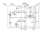
- FIG. 1is a circuit diagram showing an embodiment of an inverter topology in accordance with the present invention.
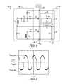
- FIG. 2is a waveform chart representing a load voltage generated by the inverter topology of FIG. 1 .
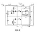
- FIG. 3is a circuit diagram showing an alternative embodiment of an inverter topology in accordance with the present invention.
- FIG. 4is a circuit diagram showing another alternative embodiment of an inverter topology in accordance with the present invention.
- FIG. 5is a circuit diagram showing another alternative embodiment of an inverter topology in accordance with the present invention.
- Coupledmeans at least either a direct electrical connection between the connected items or an indirect connection through one or more passive or active intermediary devices.
- circuitmeans at least either a single component or a multiplicity of components, either active and/or passive, that are coupled together to provide a desired function.
- signalmeans at least one current, voltage, charge, temperature, data or other signal.
- switching elementand “switch” may be used interchangeably and may refer herein to at least: a variety of transistors as known in the art (including but not limited to FET, BJT, IGBT, JFET, etc.), a switching diode, a silicon controlled rectifier (SCR), a diode for alternating current (DIAC), a triode for alternating current (TRIAC), a mechanical single pole/double pole switch (SPDT), or electrical, solid state or reed relays.
- SCRsilicon controlled rectifier
- DIACdiode for alternating current
- TRIACtriode for alternating current
- SPDTmechanical single pole/double pole switch
- FETfield effect transistor
- BJTbipolar junction transistor
- Terms such as “providing,” “processing,” “supplying,” “determining,” “calculating” or the likemay refer at least to an action of a computer system, computer program, signal processor, logic or alternative analog or digital electronic device that may be transformative of signals represented as physical quantities, whether automatically or manually initiated.
- an inverter in accordance with the present inventionincludes a pair of switching elements in a half-bridge configuration, a resonant circuit coupled to the switching elements and effective to provide an inverter output voltage to a load circuit, a clamping circuit coupled to the resonant circuit and effective to fix an operating frequency of the switching elements and further to clamp the output voltage to a constant quasi-square waveform with a predetermined amplitude, and a starting circuit to provide self-oscillation of the switching elements during a steady-state operation of the inverter.
- an inverter 10in accordance with an embodiment of the present invention includes first and second switching elements Q 1 , Q 2 arranged in a half-bridge configuration between a DC power source (V_DC), such as for example the output from a power factor correction (PFC) circuit, and an inverter ground ( 0 ).
- V_DCDC power source
- PFCpower factor correction
- a connection between the first switching element Q 1 and the DC power source V_DCmay, as described herein, further define a positive terminal 20 for the inverter 10
- a connection between the second switching element Q 2 and the inverter ground 0may, as described herein, further define a negative terminal 22 for the inverter 10 .
- a resonant circuit 12is coupled to a node between the first and second switching elements Q 1 , Q 2 , with the resonant circuit 12 as shown including a primary (first) winding Tp of a resonant inductor coupled on a first end to the node between the switching elements Q 1 , Q 2 and a resonant capacitor C 1 coupled to the second end of the primary winding Tp and to the negative terminal 22 for the inverter 10 .
- a load voltage Vload based on the output voltage Voutmay be effective to drive a load coupled to the load circuit 16 , which in various embodiments may be one or more filaments or electrodes of a lighting device such as a discharge lamp.
- the load voltage Vloadmay thus provide filament heating during a dimming or program start operation as known in the art.
- a clamping circuit 14is coupled to the resonant circuit 12 and is effective to clamp or otherwise limit the output voltage to a predetermined value whereby the output voltage and the load voltage have quasi-square waveforms regardless of the load condition.
- the clamping circuit 14as shown in FIG.
- first diode D 1having its cathode coupled to the positive terminal 20 for the inverter 10 and its anode coupled to a node between the primary winding of the resonant inductor Tp and the resonant capacitor C 1
- second diode D 2having its cathode coupled to the node between the primary winding of the resonant inductor Tp and the resonant capacitor C 1 and its anode coupled to the negative terminal 22 for the inverter 10 .
- a starting circuit 18 in an embodiment as shown in FIG. 1includes second and third secondary windings Ts 2 , Ts 3 of the resonant inductor (or alternatively stated third and fourth windings of the resonant inductor generally) which provide auxiliary feedback from the resonant circuit.
- the secondary winding Ts 2is arranged to drive the first switching element Q 1 and the secondary winding Ts 3 is arranged to drive the second switching element Q 2 .
- Resistors R 3 , R 4 , R 5 and capacitor C 2are arranged to help the switching elements Q 1 , Q 2 to begin oscillating as further described below, and resistors R 1 , R 2 may be small resistors which are arranged to reduce the oscillation on the gate drive.
- the DC power source V_DCmay charge up the capacitor C 2 in the starting circuit through the resistors R 3 , R 4 , R 5 to a value predetermined by the ratio of (R 5 /(R 3 +R 4 +R 5 )).
- the voltage across the capacitor C 2in various embodiments may be designed to turn on the first switching element Q 1 first. Once the first switching element Q 1 turns on, oscillation is initiated by the resonant circuit at the natural resonant frequency determined by the values of the resonant components Tp, C 1 .
- the voltage across the resonant capacitor C 1is clamped at maximum and minimum values (e.g., 500 Vmax and 0 Vmin).
- the voltage across the primary winding of the resonant inductor Tpwill in this case be from 500 Vmax to ⁇ 500 Vmin according to the voltage balance.
- the secondary winding Ts 2turns off the first switching element Q 1 .
- the resonant circuit(Tp, C 1 ) will continue oscillation of the switching elements Q 1 , Q 2 at the natural resonant frequency.
- the secondary winding Ts 3will turn off the second switching element Q 2 .
- the voltage across the primary winding of the resonant inductor Tpreaches a value (N*Vth, the components as described above) the voltage across the secondary winding Ts 2 turns on the first switching element Q 1 and the inverter reaches a steady-state oscillating mode.
- the voltage across the primary winding of the resonant inductor Tpwill be a quasi-square waveform with a fixed amplitude because the voltage across the resonant capacitor C 1 is clamped by the clamping circuit 14 .
- the voltage across the secondary winding Ts 1 and the load R_loadis also a quasi-square waveform with fixed amplitude as further represented in FIG. 2 .
- the clamping circuit components D 1 , D 2 and the resonant capacitor C 1may be described as further defining automatic capacitance compensation circuit.
- the equivalent capacitance (Ceq) of the capacitance compensation circuitwill be much larger than the value of the resonant capacitor C 1 , such that the actual resonant frequency of the capacitance compensation circuit and thereby the inverter itself will be less than the natural frequency of the resonant circuit: [1 ⁇ 2* ⁇ * ⁇ ( Tp*C 1)]>[1 ⁇ 2* ⁇ * ⁇ ( Tp*Ceq )
- This featuresubstantially ensures an inductive switching or soft-switching operation of the switching elements in the inverter.
- the operating frequency in an embodiment as described abovemay generally be equal to the natural resonant frequency of the resonant circuit, regardless of the load condition (i.e., whether or not there is an open circuit at the load).
- the load conditioni.e., whether or not there is an open circuit at the load.
- the inverter topology 10is similar to that represented in FIG. 1 , except that the clamping circuit 14 includes only a single diode D 1 between the resonant capacitor C 1 and the positive terminal 20 of the inverter 10 .
- both of the switching elements Q 1 , Q 2may be N-channel MOSFETs.
- the inverter topologyis similar to that represented in FIG. 1 , except that the lower side switching element (the second switching element Q 2 ) is a P-channel MOSFET.
- the starting circuit 18is further modified in such an embodiment, whereby the secondary windings Ts 2 , Ts 3 as shown in FIG. 1 are replaced with a single secondary winding Ts 2 as shown in FIG. 4 .
- the secondary winding Ts 2is coupled on a first end to the node between the switching elements Q 1 , Q 2 , and is coupled on a second end to the gate of the first switching element Q 1 and to the gate of the second switching element Q 2 .
- the inverter topology 10is similar to that represented in FIG. 4 , except that the clamping circuit 14 includes only a single diode D 1 between the resonant capacitor C 1 and the positive terminal 20 of the inverter 10 .
Landscapes
- Engineering & Computer Science (AREA)
- Power Engineering (AREA)
- Circuit Arrangements For Discharge Lamps (AREA)
- Inverter Devices (AREA)
Abstract
Description
[½*π*√(Tp*C1)]>[½*π*√(Tp*Ceq)
Claims (11)
Priority Applications (1)
| Application Number | Priority Date | Filing Date | Title |
|---|---|---|---|
| US12/915,317US8699244B1 (en) | 2010-10-29 | 2010-10-29 | Electronic ballast with load-independent and self-oscillating inverter topology |
Applications Claiming Priority (1)
| Application Number | Priority Date | Filing Date | Title |
|---|---|---|---|
| US12/915,317US8699244B1 (en) | 2010-10-29 | 2010-10-29 | Electronic ballast with load-independent and self-oscillating inverter topology |
Publications (1)
| Publication Number | Publication Date |
|---|---|
| US8699244B1true US8699244B1 (en) | 2014-04-15 |
Family
ID=50441470
Family Applications (1)
| Application Number | Title | Priority Date | Filing Date |
|---|---|---|---|
| US12/915,317Expired - Fee RelatedUS8699244B1 (en) | 2010-10-29 | 2010-10-29 | Electronic ballast with load-independent and self-oscillating inverter topology |
Country Status (1)
| Country | Link |
|---|---|
| US (1) | US8699244B1 (en) |
Cited By (3)
| Publication number | Priority date | Publication date | Assignee | Title |
|---|---|---|---|---|
| US10098202B1 (en)* | 2012-03-19 | 2018-10-09 | Universal Lighting Technologies | Constant current source with output voltage range and self-clamping output voltage |
| US11064588B1 (en) | 2019-10-07 | 2021-07-13 | Universal Lighting Technologies, Inc. | Clamped resonant tank with constant soft-switching and startup overshoot prevention |
| US20230198447A1 (en)* | 2021-12-20 | 2023-06-22 | Microchip Technology Incorporated | Circuit to provide an oscillating signal |
Citations (27)
| Publication number | Priority date | Publication date | Assignee | Title |
|---|---|---|---|---|
| US4691273A (en)* | 1986-12-11 | 1987-09-01 | Nippon Telegraph & Telephone Corp. | Series resonant converter with parallel resonant circuit |
| US4833584A (en)* | 1987-10-16 | 1989-05-23 | Wisconsin Alumni Research Foundation | Quasi-resonant current mode static power conversion method and apparatus |
| US4941076A (en)* | 1988-10-12 | 1990-07-10 | Zenith Electronics Corporation | Start-up circuit for a high voltage DC to AC converter |
| US4992919A (en)* | 1989-12-29 | 1991-02-12 | Lee Chu Quon | Parallel resonant converter with zero voltage switching |
| US5075836A (en)* | 1988-03-11 | 1991-12-24 | Origin Electric Co., Ltd. | Series resonant power converter |
| US5099407A (en)* | 1990-09-24 | 1992-03-24 | Thorne Richard L | Inverter with power factor correction circuit |
| US5349270A (en) | 1991-09-04 | 1994-09-20 | Patent-Treuhand-Gesellschaft F. Elektrische Gluehlampen Mbh | Transformerless fluorescent lamp operating circuit, particularly for a compact fluorescent lamp, with phase-shifted inverter control |
| US5448467A (en)* | 1992-04-13 | 1995-09-05 | Ferreira; Jan A. | Electrical power converter circuit |
| US5684678A (en)* | 1995-12-08 | 1997-11-04 | Delco Electronics Corp. | Resonant converter with controlled inductor |
| US5796215A (en) | 1996-01-29 | 1998-08-18 | International Rectifier Corporation | Soft start circuit for self-oscillating drivers |
| US5841240A (en) | 1995-10-20 | 1998-11-24 | U.S. Philips Corporation | Efficient discharge lamp electrode heating circuit operable over wide temperature and power range |
| US5889373A (en) | 1996-12-30 | 1999-03-30 | General Electric Company | Fluorescent lamp ballast with current feedback using a dual-function magnetic device |
| US5917289A (en) | 1997-02-04 | 1999-06-29 | General Electric Company | Lamp ballast with triggerless starting circuit |
| US5925984A (en) | 1995-12-22 | 1999-07-20 | Patent-Treuhand-Gesellschaft Fuer Elektrische Gluehlampen Mbh | Circuit arrangement having LC parallel tuned drive circuitry |
| US6031339A (en) | 1999-01-03 | 2000-02-29 | Hewlett-Packard Company | Efficient electronic ballast for fluorescent tubes |
| US6034485A (en) | 1997-11-05 | 2000-03-07 | Parra; Jorge M. | Low-voltage non-thermionic ballast-free energy-efficient light-producing gas discharge system and method |
| US6114810A (en) | 1998-01-19 | 2000-09-05 | Mass Technology (H.K.) Ltd. | Electronic ballast circuit for fluorescent lamps which have a high Q factor and high resonance voltage |
| US6150769A (en) | 1999-01-29 | 2000-11-21 | General Electric Company | Gas discharge lamp ballast with tapless feedback circuit |
| US6194840B1 (en) | 1998-12-28 | 2001-02-27 | Philips Electronics North America Corporation | Self-oscillating resonant converter with passive filter regulator |
| US6246173B1 (en) | 1997-11-18 | 2001-06-12 | Patent-Treuhand-Gesellschaft Fuer Elektrische Gluehlampen Mbh | Free-running oscillator circuit with simple starting circuit |
| US20020030451A1 (en) | 2000-02-25 | 2002-03-14 | Moisin Mihail S. | Ballast circuit having voltage clamping circuit |
| US6628090B1 (en) | 2002-05-31 | 2003-09-30 | Stmicroelectronics, S.R.L. | Resonant driving system for a fluorescent lamp |
| US6696803B2 (en) | 2000-12-14 | 2004-02-24 | Virginia Tech Intellectual Properties, Inc. | Self-oscillating electronic discharge lamp ballast with dimming control |
| US6779411B1 (en)* | 2001-12-14 | 2004-08-24 | Joe C. Spurgeon | Adaptable filter sampling device |
| US6819057B2 (en) | 2000-10-31 | 2004-11-16 | Osram Sylvania Inc. | Ballast self oscillating inverter with phase controlled voltage feedback |
| US6831423B2 (en)* | 2003-03-28 | 2004-12-14 | General Electric Company | High Q impedance matching inverter circuit with automatic line regulation |
| US6936973B2 (en) | 2002-05-31 | 2005-08-30 | Jorge M. Parra, Sr. | Self-oscillating constant-current gas discharge device lamp driver and method |
- 2010
- 2010-10-29USUS12/915,317patent/US8699244B1/ennot_activeExpired - Fee Related
Patent Citations (27)
| Publication number | Priority date | Publication date | Assignee | Title |
|---|---|---|---|---|
| US4691273A (en)* | 1986-12-11 | 1987-09-01 | Nippon Telegraph & Telephone Corp. | Series resonant converter with parallel resonant circuit |
| US4833584A (en)* | 1987-10-16 | 1989-05-23 | Wisconsin Alumni Research Foundation | Quasi-resonant current mode static power conversion method and apparatus |
| US5075836A (en)* | 1988-03-11 | 1991-12-24 | Origin Electric Co., Ltd. | Series resonant power converter |
| US4941076A (en)* | 1988-10-12 | 1990-07-10 | Zenith Electronics Corporation | Start-up circuit for a high voltage DC to AC converter |
| US4992919A (en)* | 1989-12-29 | 1991-02-12 | Lee Chu Quon | Parallel resonant converter with zero voltage switching |
| US5099407A (en)* | 1990-09-24 | 1992-03-24 | Thorne Richard L | Inverter with power factor correction circuit |
| US5349270A (en) | 1991-09-04 | 1994-09-20 | Patent-Treuhand-Gesellschaft F. Elektrische Gluehlampen Mbh | Transformerless fluorescent lamp operating circuit, particularly for a compact fluorescent lamp, with phase-shifted inverter control |
| US5448467A (en)* | 1992-04-13 | 1995-09-05 | Ferreira; Jan A. | Electrical power converter circuit |
| US5841240A (en) | 1995-10-20 | 1998-11-24 | U.S. Philips Corporation | Efficient discharge lamp electrode heating circuit operable over wide temperature and power range |
| US5684678A (en)* | 1995-12-08 | 1997-11-04 | Delco Electronics Corp. | Resonant converter with controlled inductor |
| US5925984A (en) | 1995-12-22 | 1999-07-20 | Patent-Treuhand-Gesellschaft Fuer Elektrische Gluehlampen Mbh | Circuit arrangement having LC parallel tuned drive circuitry |
| US5796215A (en) | 1996-01-29 | 1998-08-18 | International Rectifier Corporation | Soft start circuit for self-oscillating drivers |
| US5889373A (en) | 1996-12-30 | 1999-03-30 | General Electric Company | Fluorescent lamp ballast with current feedback using a dual-function magnetic device |
| US5917289A (en) | 1997-02-04 | 1999-06-29 | General Electric Company | Lamp ballast with triggerless starting circuit |
| US6034485A (en) | 1997-11-05 | 2000-03-07 | Parra; Jorge M. | Low-voltage non-thermionic ballast-free energy-efficient light-producing gas discharge system and method |
| US6246173B1 (en) | 1997-11-18 | 2001-06-12 | Patent-Treuhand-Gesellschaft Fuer Elektrische Gluehlampen Mbh | Free-running oscillator circuit with simple starting circuit |
| US6114810A (en) | 1998-01-19 | 2000-09-05 | Mass Technology (H.K.) Ltd. | Electronic ballast circuit for fluorescent lamps which have a high Q factor and high resonance voltage |
| US6194840B1 (en) | 1998-12-28 | 2001-02-27 | Philips Electronics North America Corporation | Self-oscillating resonant converter with passive filter regulator |
| US6031339A (en) | 1999-01-03 | 2000-02-29 | Hewlett-Packard Company | Efficient electronic ballast for fluorescent tubes |
| US6150769A (en) | 1999-01-29 | 2000-11-21 | General Electric Company | Gas discharge lamp ballast with tapless feedback circuit |
| US20020030451A1 (en) | 2000-02-25 | 2002-03-14 | Moisin Mihail S. | Ballast circuit having voltage clamping circuit |
| US6819057B2 (en) | 2000-10-31 | 2004-11-16 | Osram Sylvania Inc. | Ballast self oscillating inverter with phase controlled voltage feedback |
| US6696803B2 (en) | 2000-12-14 | 2004-02-24 | Virginia Tech Intellectual Properties, Inc. | Self-oscillating electronic discharge lamp ballast with dimming control |
| US6779411B1 (en)* | 2001-12-14 | 2004-08-24 | Joe C. Spurgeon | Adaptable filter sampling device |
| US6628090B1 (en) | 2002-05-31 | 2003-09-30 | Stmicroelectronics, S.R.L. | Resonant driving system for a fluorescent lamp |
| US6936973B2 (en) | 2002-05-31 | 2005-08-30 | Jorge M. Parra, Sr. | Self-oscillating constant-current gas discharge device lamp driver and method |
| US6831423B2 (en)* | 2003-03-28 | 2004-12-14 | General Electric Company | High Q impedance matching inverter circuit with automatic line regulation |
Cited By (4)
| Publication number | Priority date | Publication date | Assignee | Title |
|---|---|---|---|---|
| US10098202B1 (en)* | 2012-03-19 | 2018-10-09 | Universal Lighting Technologies | Constant current source with output voltage range and self-clamping output voltage |
| US11064588B1 (en) | 2019-10-07 | 2021-07-13 | Universal Lighting Technologies, Inc. | Clamped resonant tank with constant soft-switching and startup overshoot prevention |
| US20230198447A1 (en)* | 2021-12-20 | 2023-06-22 | Microchip Technology Incorporated | Circuit to provide an oscillating signal |
| US12255564B2 (en)* | 2021-12-20 | 2025-03-18 | Microchip Technology Incorporated | Circuit to provide an oscillating signal |
Similar Documents
| Publication | Publication Date | Title |
|---|---|---|
| US9143040B2 (en) | Hold-up time enhancement circuit for LLC resonant converter | |
| US7961482B2 (en) | Bi-directional HEMT/GaN half-bridge circuit | |
| US8274239B2 (en) | Open circuit voltage clamp for electronic HID ballast | |
| US10790762B2 (en) | Relating to power adaptors | |
| EP3195461B1 (en) | Electrodeless fluorescent ballast driving circuit and resonance circuit with added filtration and protection | |
| US9693411B1 (en) | LED driver configuration and dimming interface for dynamic adjustment of driver operating parameters | |
| US6847174B2 (en) | Drive for a half-bridge inverter | |
| US8847512B1 (en) | Program start ballast having resonant filament heating circuit with clamped quality factor | |
| US8450946B1 (en) | Zone addressing circuit for an electronic ballast | |
| US9894718B1 (en) | Constant current source LED driver circuit with self-clamped output | |
| US7098607B2 (en) | Electronic ballast with lossless snubber capacitor circuit | |
| US8699244B1 (en) | Electronic ballast with load-independent and self-oscillating inverter topology | |
| US10027233B2 (en) | Isolated single-ended primary inductor converter with voltage clamp circuit | |
| KR100994525B1 (en) | Inrush Current Reduction Circuits and Electrical Equipment | |
| JP4483867B2 (en) | Power supply | |
| US9066406B1 (en) | LED driver and protection circuit for output short conditions | |
| US8810146B1 (en) | Lighting device with circuit and method for detecting power converter activity | |
| CN109980912A (en) | A kind of easy soft starting circuit | |
| US6936974B2 (en) | Half-bridge inverter for asymmetrical loads | |
| US7432664B2 (en) | Circuit for powering a high intensity discharge lamp | |
| US20020125836A1 (en) | Inverter and lamp ignition system using the same | |
| US8324813B1 (en) | Electronic ballast with frequency independent filament voltage control | |
| US8482213B1 (en) | Electronic ballast with pulse detection circuit for lamp end of life and output short protection | |
| US8593078B1 (en) | Universal dimming ballast platform | |
| US9237617B1 (en) | LED driver with inherent current limiting and soft startup capability |
Legal Events
| Date | Code | Title | Description |
|---|---|---|---|
| AS | Assignment | Owner name:UNIVERSAL LIGHTING TECHOLOGIES, INC., ALABAMA Free format text:ASSIGNMENT OF ASSIGNORS INTEREST;ASSIGNOR:XIONG, WEI;REEL/FRAME:025767/0579 Effective date:20110121 | |
| STCF | Information on status: patent grant | Free format text:PATENTED CASE | |
| MAFP | Maintenance fee payment | Free format text:PAYMENT OF MAINTENANCE FEE, 4TH YEAR, LARGE ENTITY (ORIGINAL EVENT CODE: M1551) Year of fee payment:4 | |
| AS | Assignment | Owner name:FGI WORLDWIDE LLC, NEW YORK Free format text:SECURITY INTEREST;ASSIGNORS:UNIVERSAL LIGHTING TECHNOLOGIES, INC.;DOUGLAS LIGHTING CONTROLS, INC.;REEL/FRAME:055599/0086 Effective date:20210312 | |
| FEPP | Fee payment procedure | Free format text:MAINTENANCE FEE REMINDER MAILED (ORIGINAL EVENT CODE: REM.); ENTITY STATUS OF PATENT OWNER: LARGE ENTITY | |
| LAPS | Lapse for failure to pay maintenance fees | Free format text:PATENT EXPIRED FOR FAILURE TO PAY MAINTENANCE FEES (ORIGINAL EVENT CODE: EXP.); ENTITY STATUS OF PATENT OWNER: LARGE ENTITY | |
| STCH | Information on status: patent discontinuation | Free format text:PATENT EXPIRED DUE TO NONPAYMENT OF MAINTENANCE FEES UNDER 37 CFR 1.362 | |
| FP | Lapsed due to failure to pay maintenance fee | Effective date:20220415 |