US8697493B2 - Bonding surfaces for direct bonding of semiconductor structures - Google Patents
Bonding surfaces for direct bonding of semiconductor structuresDownload PDFInfo
- Publication number
- US8697493B2 US8697493B2US13/185,044US201113185044AUS8697493B2US 8697493 B2US8697493 B2US 8697493B2US 201113185044 AUS201113185044 AUS 201113185044AUS 8697493 B2US8697493 B2US 8697493B2
- Authority
- US
- United States
- Prior art keywords
- semiconductor structure
- dielectric material
- bonding
- semiconductor
- device structure
- Prior art date
- Legal status (The legal status is an assumption and is not a legal conclusion. Google has not performed a legal analysis and makes no representation as to the accuracy of the status listed.)
- Expired - Fee Related
Links
- 239000004065semiconductorSubstances0.000titleclaimsabstractdescription566
- 239000003989dielectric materialSubstances0.000claimsabstractdescription265
- 238000000034methodMethods0.000claimsabstractdescription172
- 230000008569processEffects0.000claimsabstractdescription102
- 239000004020conductorSubstances0.000claimsabstractdescription71
- 238000005530etchingMethods0.000claimsdescription20
- 230000000295complement effectEffects0.000claimsdescription6
- 238000007906compressionMethods0.000claimsdescription3
- 239000000463materialSubstances0.000description90
- 229910052751metalInorganic materials0.000description35
- 239000002184metalSubstances0.000description33
- 239000000203mixtureSubstances0.000description20
- 229920002120photoresistant polymerPolymers0.000description15
- 238000005498polishingMethods0.000description14
- 238000005229chemical vapour depositionMethods0.000description11
- 238000000151depositionMethods0.000description9
- RYGMFSIKBFXOCR-UHFFFAOYSA-NCopperChemical compound[Cu]RYGMFSIKBFXOCR-UHFFFAOYSA-N0.000description8
- 229910052802copperInorganic materials0.000description8
- 239000010949copperSubstances0.000description8
- 235000012431wafersNutrition0.000description8
- 229910052581Si3N4Inorganic materials0.000description7
- -1native oxides)Chemical class0.000description7
- HQVNEWCFYHHQES-UHFFFAOYSA-Nsilicon nitrideChemical compoundN12[Si]34N5[Si]62N3[Si]51N64HQVNEWCFYHHQES-UHFFFAOYSA-N0.000description7
- 238000001020plasma etchingMethods0.000description6
- 229920003229poly(methyl methacrylate)Polymers0.000description6
- 229910021420polycrystalline siliconInorganic materials0.000description6
- 239000004926polymethyl methacrylateSubstances0.000description6
- 238000003825pressingMethods0.000description6
- 230000003746surface roughnessEffects0.000description6
- 238000004519manufacturing processMethods0.000description5
- 229920005591polysiliconPolymers0.000description5
- 229910000881Cu alloyInorganic materials0.000description4
- 239000000853adhesiveSubstances0.000description4
- 230000001070adhesive effectEffects0.000description4
- 238000003486chemical etchingMethods0.000description4
- 230000010354integrationEffects0.000description4
- 239000007769metal materialSubstances0.000description4
- 238000007517polishing processMethods0.000description4
- 238000012876topographyMethods0.000description4
- 230000015572biosynthetic processEffects0.000description3
- 150000001875compoundsChemical class0.000description3
- 230000005670electromagnetic radiationEffects0.000description3
- 230000003628erosive effectEffects0.000description3
- 239000012535impuritySubstances0.000description3
- 238000000059patterningMethods0.000description3
- 238000009987spinningMethods0.000description3
- 239000000758substrateSubstances0.000description3
- 238000003631wet chemical etchingMethods0.000description3
- VYZAMTAEIAYCRO-UHFFFAOYSA-NChromiumChemical compound[Cr]VYZAMTAEIAYCRO-UHFFFAOYSA-N0.000description2
- XUIMIQQOPSSXEZ-UHFFFAOYSA-NSiliconChemical compound[Si]XUIMIQQOPSSXEZ-UHFFFAOYSA-N0.000description2
- RTAQQCXQSZGOHL-UHFFFAOYSA-NTitaniumChemical compound[Ti]RTAQQCXQSZGOHL-UHFFFAOYSA-N0.000description2
- 230000002411adverseEffects0.000description2
- 229910045601alloyInorganic materials0.000description2
- 239000000956alloySubstances0.000description2
- 229910052782aluminiumInorganic materials0.000description2
- XAGFODPZIPBFFR-UHFFFAOYSA-NaluminiumChemical compound[Al]XAGFODPZIPBFFR-UHFFFAOYSA-N0.000description2
- 230000004888barrier functionEffects0.000description2
- 229910052804chromiumInorganic materials0.000description2
- 239000011651chromiumSubstances0.000description2
- 238000009792diffusion processMethods0.000description2
- 230000007246mechanismEffects0.000description2
- 238000004377microelectronicMethods0.000description2
- 238000012986modificationMethods0.000description2
- 230000004048modificationEffects0.000description2
- 229920003023plasticPolymers0.000description2
- 239000004033plasticSubstances0.000description2
- 229910052710siliconInorganic materials0.000description2
- 239000010703siliconSubstances0.000description2
- 229910052715tantalumInorganic materials0.000description2
- GUVRBAGPIYLISA-UHFFFAOYSA-Ntantalum atomChemical compound[Ta]GUVRBAGPIYLISA-UHFFFAOYSA-N0.000description2
- 229910052719titaniumInorganic materials0.000description2
- 239000010936titaniumSubstances0.000description2
- WFKWXMTUELFFGS-UHFFFAOYSA-NtungstenChemical compound[W]WFKWXMTUELFFGS-UHFFFAOYSA-N0.000description2
- 229910052721tungstenInorganic materials0.000description2
- 239000010937tungstenSubstances0.000description2
- VYPSYNLAJGMNEJ-UHFFFAOYSA-NSilicium dioxideChemical compoundO=[Si]=OVYPSYNLAJGMNEJ-UHFFFAOYSA-N0.000description1
- 241000724291Tobacco streak virusSpecies0.000description1
- 206010044038Tooth erosionDiseases0.000description1
- 238000000137annealingMethods0.000description1
- 230000000712assemblyEffects0.000description1
- 238000000429assemblyMethods0.000description1
- 239000003990capacitorSubstances0.000description1
- 239000002131composite materialSubstances0.000description1
- 238000007772electroless platingMethods0.000description1
- 238000009713electroplatingMethods0.000description1
- 238000005516engineering processMethods0.000description1
- 230000004807localizationEffects0.000description1
- 238000004518low pressure chemical vapour depositionMethods0.000description1
- 238000002844meltingMethods0.000description1
- 230000008018meltingEffects0.000description1
- 230000005012migrationEffects0.000description1
- 238000013508migrationMethods0.000description1
- 229910052755nonmetalInorganic materials0.000description1
- 238000005289physical depositionMethods0.000description1
- 238000002360preparation methodMethods0.000description1
- 238000005204segregationMethods0.000description1
- 229910052814silicon oxideInorganic materials0.000description1
- 239000007787solidSubstances0.000description1
- 239000000126substanceSubstances0.000description1
- 238000007669thermal treatmentMethods0.000description1
Images


Classifications
- H—ELECTRICITY
- H01—ELECTRIC ELEMENTS
- H01L—SEMICONDUCTOR DEVICES NOT COVERED BY CLASS H10
- H01L24/00—Arrangements for connecting or disconnecting semiconductor or solid-state bodies; Methods or apparatus related thereto
- H01L24/80—Methods for connecting semiconductor or other solid state bodies using means for bonding being attached to, or being formed on, the surface to be connected
- H—ELECTRICITY
- H01—ELECTRIC ELEMENTS
- H01L—SEMICONDUCTOR DEVICES NOT COVERED BY CLASS H10
- H01L23/00—Details of semiconductor or other solid state devices
- H01L23/28—Encapsulations, e.g. encapsulating layers, coatings, e.g. for protection
- H01L23/31—Encapsulations, e.g. encapsulating layers, coatings, e.g. for protection characterised by the arrangement or shape
- H01L23/3157—Partial encapsulation or coating
- H01L23/3178—Coating or filling in grooves made in the semiconductor body
- H—ELECTRICITY
- H01—ELECTRIC ELEMENTS
- H01L—SEMICONDUCTOR DEVICES NOT COVERED BY CLASS H10
- H01L24/00—Arrangements for connecting or disconnecting semiconductor or solid-state bodies; Methods or apparatus related thereto
- H01L24/01—Means for bonding being attached to, or being formed on, the surface to be connected, e.g. chip-to-package, die-attach, "first-level" interconnects; Manufacturing methods related thereto
- H01L24/02—Bonding areas ; Manufacturing methods related thereto
- H01L24/03—Manufacturing methods
- H—ELECTRICITY
- H01—ELECTRIC ELEMENTS
- H01L—SEMICONDUCTOR DEVICES NOT COVERED BY CLASS H10
- H01L24/00—Arrangements for connecting or disconnecting semiconductor or solid-state bodies; Methods or apparatus related thereto
- H01L24/01—Means for bonding being attached to, or being formed on, the surface to be connected, e.g. chip-to-package, die-attach, "first-level" interconnects; Manufacturing methods related thereto
- H01L24/02—Bonding areas ; Manufacturing methods related thereto
- H01L24/04—Structure, shape, material or disposition of the bonding areas prior to the connecting process
- H01L24/05—Structure, shape, material or disposition of the bonding areas prior to the connecting process of an individual bonding area
- H—ELECTRICITY
- H01—ELECTRIC ELEMENTS
- H01L—SEMICONDUCTOR DEVICES NOT COVERED BY CLASS H10
- H01L2224/00—Indexing scheme for arrangements for connecting or disconnecting semiconductor or solid-state bodies and methods related thereto as covered by H01L24/00
- H01L2224/01—Means for bonding being attached to, or being formed on, the surface to be connected, e.g. chip-to-package, die-attach, "first-level" interconnects; Manufacturing methods related thereto
- H01L2224/02—Bonding areas; Manufacturing methods related thereto
- H01L2224/03—Manufacturing methods
- H01L2224/034—Manufacturing methods by blanket deposition of the material of the bonding area
- H01L2224/03444—Manufacturing methods by blanket deposition of the material of the bonding area in gaseous form
- H01L2224/0345—Physical vapour deposition [PVD], e.g. evaporation, or sputtering
- H—ELECTRICITY
- H01—ELECTRIC ELEMENTS
- H01L—SEMICONDUCTOR DEVICES NOT COVERED BY CLASS H10
- H01L2224/00—Indexing scheme for arrangements for connecting or disconnecting semiconductor or solid-state bodies and methods related thereto as covered by H01L24/00
- H01L2224/01—Means for bonding being attached to, or being formed on, the surface to be connected, e.g. chip-to-package, die-attach, "first-level" interconnects; Manufacturing methods related thereto
- H01L2224/02—Bonding areas; Manufacturing methods related thereto
- H01L2224/03—Manufacturing methods
- H01L2224/034—Manufacturing methods by blanket deposition of the material of the bonding area
- H01L2224/03444—Manufacturing methods by blanket deposition of the material of the bonding area in gaseous form
- H01L2224/03452—Chemical vapour deposition [CVD], e.g. laser CVD
- H—ELECTRICITY
- H01—ELECTRIC ELEMENTS
- H01L—SEMICONDUCTOR DEVICES NOT COVERED BY CLASS H10
- H01L2224/00—Indexing scheme for arrangements for connecting or disconnecting semiconductor or solid-state bodies and methods related thereto as covered by H01L24/00
- H01L2224/01—Means for bonding being attached to, or being formed on, the surface to be connected, e.g. chip-to-package, die-attach, "first-level" interconnects; Manufacturing methods related thereto
- H01L2224/02—Bonding areas; Manufacturing methods related thereto
- H01L2224/03—Manufacturing methods
- H01L2224/036—Manufacturing methods by patterning a pre-deposited material
- H01L2224/0361—Physical or chemical etching
- H01L2224/03616—Chemical mechanical polishing [CMP]
- H—ELECTRICITY
- H01—ELECTRIC ELEMENTS
- H01L—SEMICONDUCTOR DEVICES NOT COVERED BY CLASS H10
- H01L2224/00—Indexing scheme for arrangements for connecting or disconnecting semiconductor or solid-state bodies and methods related thereto as covered by H01L24/00
- H01L2224/01—Means for bonding being attached to, or being formed on, the surface to be connected, e.g. chip-to-package, die-attach, "first-level" interconnects; Manufacturing methods related thereto
- H01L2224/02—Bonding areas; Manufacturing methods related thereto
- H01L2224/03—Manufacturing methods
- H01L2224/038—Post-treatment of the bonding area
- H01L2224/0383—Reworking, e.g. shaping
- H01L2224/03831—Reworking, e.g. shaping involving a chemical process, e.g. etching the bonding area
- H—ELECTRICITY
- H01—ELECTRIC ELEMENTS
- H01L—SEMICONDUCTOR DEVICES NOT COVERED BY CLASS H10
- H01L2224/00—Indexing scheme for arrangements for connecting or disconnecting semiconductor or solid-state bodies and methods related thereto as covered by H01L24/00
- H01L2224/01—Means for bonding being attached to, or being formed on, the surface to be connected, e.g. chip-to-package, die-attach, "first-level" interconnects; Manufacturing methods related thereto
- H01L2224/02—Bonding areas; Manufacturing methods related thereto
- H01L2224/03—Manufacturing methods
- H01L2224/038—Post-treatment of the bonding area
- H01L2224/0383—Reworking, e.g. shaping
- H01L2224/03845—Chemical mechanical polishing [CMP]
- H—ELECTRICITY
- H01—ELECTRIC ELEMENTS
- H01L—SEMICONDUCTOR DEVICES NOT COVERED BY CLASS H10
- H01L2224/00—Indexing scheme for arrangements for connecting or disconnecting semiconductor or solid-state bodies and methods related thereto as covered by H01L24/00
- H01L2224/01—Means for bonding being attached to, or being formed on, the surface to be connected, e.g. chip-to-package, die-attach, "first-level" interconnects; Manufacturing methods related thereto
- H01L2224/02—Bonding areas; Manufacturing methods related thereto
- H01L2224/03—Manufacturing methods
- H01L2224/039—Methods of manufacturing bonding areas involving a specific sequence of method steps
- H01L2224/0391—Forming a passivation layer after forming the bonding area
- H—ELECTRICITY
- H01—ELECTRIC ELEMENTS
- H01L—SEMICONDUCTOR DEVICES NOT COVERED BY CLASS H10
- H01L2224/00—Indexing scheme for arrangements for connecting or disconnecting semiconductor or solid-state bodies and methods related thereto as covered by H01L24/00
- H01L2224/01—Means for bonding being attached to, or being formed on, the surface to be connected, e.g. chip-to-package, die-attach, "first-level" interconnects; Manufacturing methods related thereto
- H01L2224/02—Bonding areas; Manufacturing methods related thereto
- H01L2224/04—Structure, shape, material or disposition of the bonding areas prior to the connecting process
- H01L2224/05—Structure, shape, material or disposition of the bonding areas prior to the connecting process of an individual bonding area
- H01L2224/0554—External layer
- H01L2224/0555—Shape
- H01L2224/05556—Shape in side view
- H01L2224/05557—Shape in side view comprising protrusions or indentations
- H—ELECTRICITY
- H01—ELECTRIC ELEMENTS
- H01L—SEMICONDUCTOR DEVICES NOT COVERED BY CLASS H10
- H01L2224/00—Indexing scheme for arrangements for connecting or disconnecting semiconductor or solid-state bodies and methods related thereto as covered by H01L24/00
- H01L2224/01—Means for bonding being attached to, or being formed on, the surface to be connected, e.g. chip-to-package, die-attach, "first-level" interconnects; Manufacturing methods related thereto
- H01L2224/02—Bonding areas; Manufacturing methods related thereto
- H01L2224/04—Structure, shape, material or disposition of the bonding areas prior to the connecting process
- H01L2224/05—Structure, shape, material or disposition of the bonding areas prior to the connecting process of an individual bonding area
- H01L2224/0554—External layer
- H01L2224/0556—Disposition
- H01L2224/05571—Disposition the external layer being disposed in a recess of the surface
- H01L2224/05572—Disposition the external layer being disposed in a recess of the surface the external layer extending out of an opening
- H—ELECTRICITY
- H01—ELECTRIC ELEMENTS
- H01L—SEMICONDUCTOR DEVICES NOT COVERED BY CLASS H10
- H01L2224/00—Indexing scheme for arrangements for connecting or disconnecting semiconductor or solid-state bodies and methods related thereto as covered by H01L24/00
- H01L2224/01—Means for bonding being attached to, or being formed on, the surface to be connected, e.g. chip-to-package, die-attach, "first-level" interconnects; Manufacturing methods related thereto
- H01L2224/02—Bonding areas; Manufacturing methods related thereto
- H01L2224/04—Structure, shape, material or disposition of the bonding areas prior to the connecting process
- H01L2224/05—Structure, shape, material or disposition of the bonding areas prior to the connecting process of an individual bonding area
- H01L2224/0554—External layer
- H01L2224/05573—Single external layer
- H—ELECTRICITY
- H01—ELECTRIC ELEMENTS
- H01L—SEMICONDUCTOR DEVICES NOT COVERED BY CLASS H10
- H01L2224/00—Indexing scheme for arrangements for connecting or disconnecting semiconductor or solid-state bodies and methods related thereto as covered by H01L24/00
- H01L2224/01—Means for bonding being attached to, or being formed on, the surface to be connected, e.g. chip-to-package, die-attach, "first-level" interconnects; Manufacturing methods related thereto
- H01L2224/02—Bonding areas; Manufacturing methods related thereto
- H01L2224/04—Structure, shape, material or disposition of the bonding areas prior to the connecting process
- H01L2224/05—Structure, shape, material or disposition of the bonding areas prior to the connecting process of an individual bonding area
- H01L2224/0554—External layer
- H01L2224/05599—Material
- H01L2224/056—Material with a principal constituent of the material being a metal or a metalloid, e.g. boron [B], silicon [Si], germanium [Ge], arsenic [As], antimony [Sb], tellurium [Te] and polonium [Po], and alloys thereof
- H01L2224/05617—Material with a principal constituent of the material being a metal or a metalloid, e.g. boron [B], silicon [Si], germanium [Ge], arsenic [As], antimony [Sb], tellurium [Te] and polonium [Po], and alloys thereof the principal constituent melting at a temperature of greater than or equal to 400°C and less than 950°C
- H01L2224/05624—Aluminium [Al] as principal constituent
- H—ELECTRICITY
- H01—ELECTRIC ELEMENTS
- H01L—SEMICONDUCTOR DEVICES NOT COVERED BY CLASS H10
- H01L2224/00—Indexing scheme for arrangements for connecting or disconnecting semiconductor or solid-state bodies and methods related thereto as covered by H01L24/00
- H01L2224/01—Means for bonding being attached to, or being formed on, the surface to be connected, e.g. chip-to-package, die-attach, "first-level" interconnects; Manufacturing methods related thereto
- H01L2224/02—Bonding areas; Manufacturing methods related thereto
- H01L2224/04—Structure, shape, material or disposition of the bonding areas prior to the connecting process
- H01L2224/05—Structure, shape, material or disposition of the bonding areas prior to the connecting process of an individual bonding area
- H01L2224/0554—External layer
- H01L2224/05599—Material
- H01L2224/056—Material with a principal constituent of the material being a metal or a metalloid, e.g. boron [B], silicon [Si], germanium [Ge], arsenic [As], antimony [Sb], tellurium [Te] and polonium [Po], and alloys thereof
- H01L2224/05638—Material with a principal constituent of the material being a metal or a metalloid, e.g. boron [B], silicon [Si], germanium [Ge], arsenic [As], antimony [Sb], tellurium [Te] and polonium [Po], and alloys thereof the principal constituent melting at a temperature of greater than or equal to 950°C and less than 1550°C
- H01L2224/05647—Copper [Cu] as principal constituent
- H—ELECTRICITY
- H01—ELECTRIC ELEMENTS
- H01L—SEMICONDUCTOR DEVICES NOT COVERED BY CLASS H10
- H01L2224/00—Indexing scheme for arrangements for connecting or disconnecting semiconductor or solid-state bodies and methods related thereto as covered by H01L24/00
- H01L2224/01—Means for bonding being attached to, or being formed on, the surface to be connected, e.g. chip-to-package, die-attach, "first-level" interconnects; Manufacturing methods related thereto
- H01L2224/02—Bonding areas; Manufacturing methods related thereto
- H01L2224/04—Structure, shape, material or disposition of the bonding areas prior to the connecting process
- H01L2224/05—Structure, shape, material or disposition of the bonding areas prior to the connecting process of an individual bonding area
- H01L2224/0554—External layer
- H01L2224/05599—Material
- H01L2224/056—Material with a principal constituent of the material being a metal or a metalloid, e.g. boron [B], silicon [Si], germanium [Ge], arsenic [As], antimony [Sb], tellurium [Te] and polonium [Po], and alloys thereof
- H01L2224/05663—Material with a principal constituent of the material being a metal or a metalloid, e.g. boron [B], silicon [Si], germanium [Ge], arsenic [As], antimony [Sb], tellurium [Te] and polonium [Po], and alloys thereof the principal constituent melting at a temperature of greater than 1550°C
- H01L2224/05666—Titanium [Ti] as principal constituent
- H—ELECTRICITY
- H01—ELECTRIC ELEMENTS
- H01L—SEMICONDUCTOR DEVICES NOT COVERED BY CLASS H10
- H01L2224/00—Indexing scheme for arrangements for connecting or disconnecting semiconductor or solid-state bodies and methods related thereto as covered by H01L24/00
- H01L2224/01—Means for bonding being attached to, or being formed on, the surface to be connected, e.g. chip-to-package, die-attach, "first-level" interconnects; Manufacturing methods related thereto
- H01L2224/02—Bonding areas; Manufacturing methods related thereto
- H01L2224/04—Structure, shape, material or disposition of the bonding areas prior to the connecting process
- H01L2224/05—Structure, shape, material or disposition of the bonding areas prior to the connecting process of an individual bonding area
- H01L2224/0554—External layer
- H01L2224/05599—Material
- H01L2224/056—Material with a principal constituent of the material being a metal or a metalloid, e.g. boron [B], silicon [Si], germanium [Ge], arsenic [As], antimony [Sb], tellurium [Te] and polonium [Po], and alloys thereof
- H01L2224/05663—Material with a principal constituent of the material being a metal or a metalloid, e.g. boron [B], silicon [Si], germanium [Ge], arsenic [As], antimony [Sb], tellurium [Te] and polonium [Po], and alloys thereof the principal constituent melting at a temperature of greater than 1550°C
- H01L2224/05671—Chromium [Cr] as principal constituent
- H—ELECTRICITY
- H01—ELECTRIC ELEMENTS
- H01L—SEMICONDUCTOR DEVICES NOT COVERED BY CLASS H10
- H01L2224/00—Indexing scheme for arrangements for connecting or disconnecting semiconductor or solid-state bodies and methods related thereto as covered by H01L24/00
- H01L2224/01—Means for bonding being attached to, or being formed on, the surface to be connected, e.g. chip-to-package, die-attach, "first-level" interconnects; Manufacturing methods related thereto
- H01L2224/02—Bonding areas; Manufacturing methods related thereto
- H01L2224/04—Structure, shape, material or disposition of the bonding areas prior to the connecting process
- H01L2224/05—Structure, shape, material or disposition of the bonding areas prior to the connecting process of an individual bonding area
- H01L2224/0554—External layer
- H01L2224/05599—Material
- H01L2224/056—Material with a principal constituent of the material being a metal or a metalloid, e.g. boron [B], silicon [Si], germanium [Ge], arsenic [As], antimony [Sb], tellurium [Te] and polonium [Po], and alloys thereof
- H01L2224/05663—Material with a principal constituent of the material being a metal or a metalloid, e.g. boron [B], silicon [Si], germanium [Ge], arsenic [As], antimony [Sb], tellurium [Te] and polonium [Po], and alloys thereof the principal constituent melting at a temperature of greater than 1550°C
- H01L2224/05681—Tantalum [Ta] as principal constituent
- H—ELECTRICITY
- H01—ELECTRIC ELEMENTS
- H01L—SEMICONDUCTOR DEVICES NOT COVERED BY CLASS H10
- H01L2224/00—Indexing scheme for arrangements for connecting or disconnecting semiconductor or solid-state bodies and methods related thereto as covered by H01L24/00
- H01L2224/01—Means for bonding being attached to, or being formed on, the surface to be connected, e.g. chip-to-package, die-attach, "first-level" interconnects; Manufacturing methods related thereto
- H01L2224/02—Bonding areas; Manufacturing methods related thereto
- H01L2224/04—Structure, shape, material or disposition of the bonding areas prior to the connecting process
- H01L2224/05—Structure, shape, material or disposition of the bonding areas prior to the connecting process of an individual bonding area
- H01L2224/0554—External layer
- H01L2224/05599—Material
- H01L2224/056—Material with a principal constituent of the material being a metal or a metalloid, e.g. boron [B], silicon [Si], germanium [Ge], arsenic [As], antimony [Sb], tellurium [Te] and polonium [Po], and alloys thereof
- H01L2224/05663—Material with a principal constituent of the material being a metal or a metalloid, e.g. boron [B], silicon [Si], germanium [Ge], arsenic [As], antimony [Sb], tellurium [Te] and polonium [Po], and alloys thereof the principal constituent melting at a temperature of greater than 1550°C
- H01L2224/05684—Tungsten [W] as principal constituent
- H—ELECTRICITY
- H01—ELECTRIC ELEMENTS
- H01L—SEMICONDUCTOR DEVICES NOT COVERED BY CLASS H10
- H01L2224/00—Indexing scheme for arrangements for connecting or disconnecting semiconductor or solid-state bodies and methods related thereto as covered by H01L24/00
- H01L2224/01—Means for bonding being attached to, or being formed on, the surface to be connected, e.g. chip-to-package, die-attach, "first-level" interconnects; Manufacturing methods related thereto
- H01L2224/02—Bonding areas; Manufacturing methods related thereto
- H01L2224/07—Structure, shape, material or disposition of the bonding areas after the connecting process
- H01L2224/08—Structure, shape, material or disposition of the bonding areas after the connecting process of an individual bonding area
- H01L2224/0805—Shape
- H01L2224/0807—Shape of bonding interfaces, e.g. interlocking features
- H—ELECTRICITY
- H01—ELECTRIC ELEMENTS
- H01L—SEMICONDUCTOR DEVICES NOT COVERED BY CLASS H10
- H01L2224/00—Indexing scheme for arrangements for connecting or disconnecting semiconductor or solid-state bodies and methods related thereto as covered by H01L24/00
- H01L2224/01—Means for bonding being attached to, or being formed on, the surface to be connected, e.g. chip-to-package, die-attach, "first-level" interconnects; Manufacturing methods related thereto
- H01L2224/02—Bonding areas; Manufacturing methods related thereto
- H01L2224/07—Structure, shape, material or disposition of the bonding areas after the connecting process
- H01L2224/08—Structure, shape, material or disposition of the bonding areas after the connecting process of an individual bonding area
- H01L2224/081—Disposition
- H01L2224/0812—Disposition the bonding area connecting directly to another bonding area, i.e. connectorless bonding, e.g. bumpless bonding
- H01L2224/08135—Disposition the bonding area connecting directly to another bonding area, i.e. connectorless bonding, e.g. bumpless bonding the bonding area connecting between different semiconductor or solid-state bodies, i.e. chip-to-chip
- H01L2224/08145—Disposition the bonding area connecting directly to another bonding area, i.e. connectorless bonding, e.g. bumpless bonding the bonding area connecting between different semiconductor or solid-state bodies, i.e. chip-to-chip the bodies being stacked
- H01L2224/08147—Disposition the bonding area connecting directly to another bonding area, i.e. connectorless bonding, e.g. bumpless bonding the bonding area connecting between different semiconductor or solid-state bodies, i.e. chip-to-chip the bodies being stacked the bonding area connecting to a bonding area disposed in a recess of the surface of the body
- H—ELECTRICITY
- H01—ELECTRIC ELEMENTS
- H01L—SEMICONDUCTOR DEVICES NOT COVERED BY CLASS H10
- H01L2224/00—Indexing scheme for arrangements for connecting or disconnecting semiconductor or solid-state bodies and methods related thereto as covered by H01L24/00
- H01L2224/01—Means for bonding being attached to, or being formed on, the surface to be connected, e.g. chip-to-package, die-attach, "first-level" interconnects; Manufacturing methods related thereto
- H01L2224/02—Bonding areas; Manufacturing methods related thereto
- H01L2224/07—Structure, shape, material or disposition of the bonding areas after the connecting process
- H01L2224/08—Structure, shape, material or disposition of the bonding areas after the connecting process of an individual bonding area
- H01L2224/081—Disposition
- H01L2224/0812—Disposition the bonding area connecting directly to another bonding area, i.e. connectorless bonding, e.g. bumpless bonding
- H01L2224/08135—Disposition the bonding area connecting directly to another bonding area, i.e. connectorless bonding, e.g. bumpless bonding the bonding area connecting between different semiconductor or solid-state bodies, i.e. chip-to-chip
- H01L2224/08145—Disposition the bonding area connecting directly to another bonding area, i.e. connectorless bonding, e.g. bumpless bonding the bonding area connecting between different semiconductor or solid-state bodies, i.e. chip-to-chip the bodies being stacked
- H01L2224/08148—Disposition the bonding area connecting directly to another bonding area, i.e. connectorless bonding, e.g. bumpless bonding the bonding area connecting between different semiconductor or solid-state bodies, i.e. chip-to-chip the bodies being stacked the bonding area connecting to a bonding area protruding from the surface of the body
- H—ELECTRICITY
- H01—ELECTRIC ELEMENTS
- H01L—SEMICONDUCTOR DEVICES NOT COVERED BY CLASS H10
- H01L2224/00—Indexing scheme for arrangements for connecting or disconnecting semiconductor or solid-state bodies and methods related thereto as covered by H01L24/00
- H01L2224/80—Methods for connecting semiconductor or other solid state bodies using means for bonding being attached to, or being formed on, the surface to be connected
- H01L2224/80001—Methods for connecting semiconductor or other solid state bodies using means for bonding being attached to, or being formed on, the surface to be connected by connecting a bonding area directly to another bonding area, i.e. connectorless bonding, e.g. bumpless bonding
- H01L2224/80053—Bonding environment
- H01L2224/80095—Temperature settings
- H01L2224/80096—Transient conditions
- H01L2224/80097—Heating
- H—ELECTRICITY
- H01—ELECTRIC ELEMENTS
- H01L—SEMICONDUCTOR DEVICES NOT COVERED BY CLASS H10
- H01L2224/00—Indexing scheme for arrangements for connecting or disconnecting semiconductor or solid-state bodies and methods related thereto as covered by H01L24/00
- H01L2224/80—Methods for connecting semiconductor or other solid state bodies using means for bonding being attached to, or being formed on, the surface to be connected
- H01L2224/80001—Methods for connecting semiconductor or other solid state bodies using means for bonding being attached to, or being formed on, the surface to be connected by connecting a bonding area directly to another bonding area, i.e. connectorless bonding, e.g. bumpless bonding
- H01L2224/8012—Aligning
- H01L2224/80136—Aligning involving guiding structures, e.g. spacers or supporting members
- H01L2224/80138—Aligning involving guiding structures, e.g. spacers or supporting members the guiding structures being at least partially left in the finished device
- H01L2224/80141—Guiding structures both on and outside the body
- H—ELECTRICITY
- H01—ELECTRIC ELEMENTS
- H01L—SEMICONDUCTOR DEVICES NOT COVERED BY CLASS H10
- H01L2224/00—Indexing scheme for arrangements for connecting or disconnecting semiconductor or solid-state bodies and methods related thereto as covered by H01L24/00
- H01L2224/80—Methods for connecting semiconductor or other solid state bodies using means for bonding being attached to, or being formed on, the surface to be connected
- H01L2224/80001—Methods for connecting semiconductor or other solid state bodies using means for bonding being attached to, or being formed on, the surface to be connected by connecting a bonding area directly to another bonding area, i.e. connectorless bonding, e.g. bumpless bonding
- H01L2224/8034—Bonding interfaces of the bonding area
- H01L2224/80357—Bonding interfaces of the bonding area being flush with the surface
- H—ELECTRICITY
- H01—ELECTRIC ELEMENTS
- H01L—SEMICONDUCTOR DEVICES NOT COVERED BY CLASS H10
- H01L2224/00—Indexing scheme for arrangements for connecting or disconnecting semiconductor or solid-state bodies and methods related thereto as covered by H01L24/00
- H01L2224/80—Methods for connecting semiconductor or other solid state bodies using means for bonding being attached to, or being formed on, the surface to be connected
- H01L2224/80001—Methods for connecting semiconductor or other solid state bodies using means for bonding being attached to, or being formed on, the surface to be connected by connecting a bonding area directly to another bonding area, i.e. connectorless bonding, e.g. bumpless bonding
- H01L2224/8036—Bonding interfaces of the semiconductor or solid state body
- H01L2224/80365—Shape, e.g. interlocking features
- H—ELECTRICITY
- H01—ELECTRIC ELEMENTS
- H01L—SEMICONDUCTOR DEVICES NOT COVERED BY CLASS H10
- H01L2224/00—Indexing scheme for arrangements for connecting or disconnecting semiconductor or solid-state bodies and methods related thereto as covered by H01L24/00
- H01L2224/80—Methods for connecting semiconductor or other solid state bodies using means for bonding being attached to, or being formed on, the surface to be connected
- H01L2224/80001—Methods for connecting semiconductor or other solid state bodies using means for bonding being attached to, or being formed on, the surface to be connected by connecting a bonding area directly to another bonding area, i.e. connectorless bonding, e.g. bumpless bonding
- H01L2224/808—Bonding techniques
- H01L2224/80894—Direct bonding, i.e. joining surfaces by means of intermolecular attracting interactions at their interfaces, e.g. covalent bonds, van der Waals forces
- H01L2224/80895—Direct bonding, i.e. joining surfaces by means of intermolecular attracting interactions at their interfaces, e.g. covalent bonds, van der Waals forces between electrically conductive surfaces, e.g. copper-copper direct bonding, surface activated bonding
- H—ELECTRICITY
- H01—ELECTRIC ELEMENTS
- H01L—SEMICONDUCTOR DEVICES NOT COVERED BY CLASS H10
- H01L2224/00—Indexing scheme for arrangements for connecting or disconnecting semiconductor or solid-state bodies and methods related thereto as covered by H01L24/00
- H01L2224/80—Methods for connecting semiconductor or other solid state bodies using means for bonding being attached to, or being formed on, the surface to be connected
- H01L2224/80001—Methods for connecting semiconductor or other solid state bodies using means for bonding being attached to, or being formed on, the surface to be connected by connecting a bonding area directly to another bonding area, i.e. connectorless bonding, e.g. bumpless bonding
- H01L2224/808—Bonding techniques
- H01L2224/80894—Direct bonding, i.e. joining surfaces by means of intermolecular attracting interactions at their interfaces, e.g. covalent bonds, van der Waals forces
- H01L2224/80896—Direct bonding, i.e. joining surfaces by means of intermolecular attracting interactions at their interfaces, e.g. covalent bonds, van der Waals forces between electrically insulating surfaces, e.g. oxide or nitride layers
- H—ELECTRICITY
- H01—ELECTRIC ELEMENTS
- H01L—SEMICONDUCTOR DEVICES NOT COVERED BY CLASS H10
- H01L2224/00—Indexing scheme for arrangements for connecting or disconnecting semiconductor or solid-state bodies and methods related thereto as covered by H01L24/00
- H01L2224/80—Methods for connecting semiconductor or other solid state bodies using means for bonding being attached to, or being formed on, the surface to be connected
- H01L2224/80001—Methods for connecting semiconductor or other solid state bodies using means for bonding being attached to, or being formed on, the surface to be connected by connecting a bonding area directly to another bonding area, i.e. connectorless bonding, e.g. bumpless bonding
- H01L2224/80986—Specific sequence of steps, e.g. repetition of manufacturing steps, time sequence
- H—ELECTRICITY
- H01—ELECTRIC ELEMENTS
- H01L—SEMICONDUCTOR DEVICES NOT COVERED BY CLASS H10
- H01L2924/00—Indexing scheme for arrangements or methods for connecting or disconnecting semiconductor or solid-state bodies as covered by H01L24/00
- H01L2924/0001—Technical content checked by a classifier
- H01L2924/00014—Technical content checked by a classifier the subject-matter covered by the group, the symbol of which is combined with the symbol of this group, being disclosed without further technical details
Definitions
- the present inventionrelates to methods of directly bonding together semiconductor structures, and to bonded semiconductor structures formed using such methods.
- the three-dimensional (3D) integration of two or more semiconductor structurescan produce a number of benefits to microelectronic applications.
- 3D integration of microelectronic componentscan result in improved electrical performance and power consumption while reducing the area of the device foot print. See, for example, P. Garrou, et al., “The Handbook of 3D Integration,” Wiley-VCH (2008).
- the 3D integration of semiconductor structuresmay take place by the attachment of a semiconductor die to one or more additional semiconductor dies (i.e., die-to-die (D2D)), a semiconductor die to one or more semiconductor wafers (i.e., die-to-wafer (D2W)), as well as a semiconductor wafer to one or more additional semiconductor wafers (i.e., wafer-to-wafer (W2W)), or a combination thereof.
- D2Ddie-to-die
- D2Wdie-to-wafer
- W2Wwafer-to-wafer
- the bonding techniques used in bonding one semiconductor structure to another semiconductor structuremay be categorized in different ways, one being whether a layer of intermediate material is provided between the two semiconductor structures to bond them together, and the second being whether the bonding interface allows electrons (i.e., electrical current) to pass through the interface.
- So called “direct bonding methods”are methods in which a direct solid-to-solid chemical bond is established between two semiconductor structures to bond them together without using an intermediate bonding material between the two semiconductor structures to bond them together.
- Direct metal-to-metal bonding methodshave been developed for bonding metal material at a surface of a first semiconductor structure to metal material at a surface of a second semiconductor structure.
- Direct metal-to-metal bonding methodsmay also be categorized by the temperature range in which each is carried out. For example, some direct metal-to-metal bonding methods are carried out at relatively high temperatures resulting in at least partial melting of the metal material at the bonding interface. Such direct bonding processes may be undesirable for use in bonding processed semiconductor structures that include one or more device structures, as the relatively high temperatures may adversely affect the earlier formed device structures.
- “Thermo-compression bonding” methodsare direct bonding methods in which pressure is applied between the bonding surfaces at elevated temperatures between two hundred degrees Celsius (200° C.) and about five hundred degrees Celsius (500° C.), and often between about three hundred degrees Celsius (300° C.) and about four hundred degrees Celsius (400° C.).
- Ultra-low temperature direct bonding methodsmay be carried out by careful removal of surface impurities and surface compounds (e.g., native oxides), and by increasing the area of intimate contact between the two surfaces at the atomic scale. The area of intimate contact between the two surfaces is generally accomplished by polishing the bonding surfaces to reduce the surface roughness up to values close to the atomic scale, by applying pressure between the bonding surfaces resulting in plastic deformation, or by both polishing the bonding surfaces and applying pressure to attain such plastic deformation.
- surface impurities and surface compoundse.g., native oxides
- ultra-low temperature direct bonding methodsmay be carried out without applying pressure between the bonding surfaces at the bonding interface, although pressure may be applied between the bonding surfaces at the bonding interface in other ultra-low temperature direct bonding methods in order to achieve a suitable bond strength at the bonding interface.
- Ultra-low temperature direct bonding methods in which pressure is applied between the bonding surfacesare often referred to in the art as “surface assisted bonding” or “SAB” methods.
- the terms “surface assisted bonding” and “SAB”mean and include any direct bonding process in which a first material is directly bonded to a second material by abutting the first material against the second material and applying pressure between the bonding surfaces at the bonding interface at a temperature of two hundred degrees Celsius (200° C.) or less.
- Direct metal-to-metal bonds between active conductive features in semiconductor structuresmay, in some instances, be prone to mechanical failure or electrical failure after a period of time even though an acceptable direct metal-to-metal bond may be initially established between the conductive features of the semiconductor structures.
- failuremay be at least partially caused by one or more of three related mechanisms.
- the three related mechanismsare strain localization, which may be promoted by large grains, deformation-associated grain growth, and mass transport at the bonding interface. Such mass transport at the bonding interface may be at least partially due to electromigration, phase segregation, etc.
- Electromigrationis the migration of metal atoms in a conductive material due to an electrical current.
- Various methods for improving the electromigration lifetime of interconnectshave been discussed in the art. For example, methods for improving the electromagnetic lifetime of copper interconnects are discussed in J. Gambino et al., “Copper Interconnect Technology for the 32 nm Node and Beyond,” IEEE 2009 Custom Integrated Circuits Conference (CICC), pages 141-148.
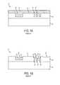
- FIGS. 1A and 1Billustrate a problem that may be encountered in direct bonding methods.
- a semiconductor structure 10is illustrated that includes a device layer 12 , which may comprise a plurality of device structures, although such structures are not illustrated in the simplified figures.
- Dielectric material 14is disposed over the device layer 12 , and a plurality of recesses 16 extend into the dielectric material 14 at locations at which it is desired to form conductive elements such as conductive pads, traces, vias, etc.
- electrically conductive metal 18e.g., copper or a copper alloy
- Excess conductive metal 18is often deposited, such that a layer of the conductive metal 18 extends over the major upper surface 15 of the dielectric material 14 , as shown in FIG. 1A .
- the excess conductive metal 18is removed from the major upper surface 15 of the dielectric material 14 to form a semiconductor structure 20 as shown in FIG. 1B . Removal of the excess conductive metal 18 defines device structures 22 that comprise the conductive metal 18 in the recesses 16 .
- CMPchemical-mechanical polishing
- the CMP process used to remove the excess conductive metal 18 from the major upper surface 15 of the dielectric material 14may result in the exposed surfaces 23 of the device structures 22 being recessed relative to the surrounding major upper surface 15 of the dielectric material 14 .
- the exposed surfaces 23may have an arcuate, concave shape as shown in FIG. 1B . This phenomenon is often referred to in the art as “dishing.”
- the CMP process used to remove the excess conductive metal 18 from the major upper surface 15 of the dielectric material 14also may cause excessive removal of the dielectric material 14 at certain locations, such as the locations 26 between closely separated device structures 22 , as well as random locations on the major upper surface 15 of the dielectric material 14 , such as the location 28 shown in FIG. 1B .
- Dishing of the exposed surfaces 23 of the device structures 22 and localized erosion of the major upper surface 15 of the dielectric material 14may adversely affect the strength of a bond and electrical connection subsequently established between the semiconductor structure 20 of FIG. 1B and another semiconductor structure (not shown) in a direct bonding process.
- the present inventionincludes methods of directly bonding a first semiconductor structure to a second semiconductor structure.
- a first semiconductor structuremay be provided that includes at least one device structure comprising a conductive material (e.g., a metal or a conductive non-metal material such as polycrystalline silicon, which is often referred to as “polysilicon”), and a dielectric material disposed adjacent the at least one device structure.
- the at least one device structure and the dielectric materialmay be exposed at a bonding surface of the first semiconductor structure.
- An exposed surface of the dielectric material at the bonding surface of the first semiconductor structuremay define a bond plane of the first semiconductor structure.
- the at least one device structure of the first semiconductor structuremay be caused to project a distance from the bond plane of the first semiconductor structure beyond the adjacent dielectric material.
- a second semiconductor structuremay be provided that includes at least one device structure comprising a conductive material, and a dielectric material disposed adjacent the at least one device structure. The at least one device structure and the dielectric material may be exposed at a bonding surface of the second semiconductor structure. An exposed surface of the dielectric material at the bonding surface of the second semiconductor structure may define a bond plane of the second semiconductor structure.
- the at least one device structure of the first semiconductor structuremay be bonded directly to the at least one device structure of the second semiconductor structure in a metal-to-metal direct bonding process.
- Additional embodiments of methods of directly bonding a first semiconductor structure to a second semiconductor structureinclude providing a first semiconductor structure, providing a second semiconductor structure, and bonding a plurality of integral protrusions of at least one device structure of the first semiconductor structure directly to a plurality of integral protrusions of the at least one device structure of the second semiconductor structure in a conductive material-to-conductive material direct bonding process (e.g., metal-to-metal, polysilicon-to-polysilicon, polysilicon-to-metal, etc.).
- the first semiconductor structuremay comprise the at least one device structure, which may comprise a conductive material, and a dielectric material disposed adjacent the at least one device structure.
- the at least one device structureincludes a plurality of integral protrusions extending from a base structure.
- the plurality of integral protrusions and the dielectric materialare exposed at a bonding surface of the first semiconductor structure.
- the dielectric materialextends over a portion of the at least one device structure between the integral protrusions of the at least one device structure.
- An exposed surface of the dielectric material at the bonding surface of the first semiconductor structuredefines a bond plane of the first semiconductor structure.
- the second semiconductor structurealso includes at least one device structure, which may comprise a conductive material, and a dielectric material disposed adjacent the at least one device structure.
- the at least one device structurecomprises a plurality of integral protrusions extending from a base structure.
- the plurality of integral protrusions and the dielectric materialare exposed at a bonding surface of the second semiconductor structure.
- the dielectric material of the second semiconductor structureextends over a portion of the at least one device structure between the integral protrusions of the plurality of integral protrusions of the at least one device structure of the second semiconductor structure.
- An exposed surface of the dielectric material at the bonding surface of the second semiconductor structuredefines a bond plane of the second semiconductor structure.
- the present inventionincludes bonded semiconductor structures.
- the bonded semiconductor structuresinclude a first semiconductor structure bonded to a second semiconductor structure.
- the first semiconductor structureincludes at least one conductive device structure at a bonding surface of the first semiconductor structure, and a dielectric material disposed adjacent the at least one conductive device structure at the bonding surface of the first semiconductor structure.
- the second semiconductor structurealso includes at least one conductive device structure at a bonding surface of the second semiconductor structure, and a dielectric material disposed adjacent the at least one conductive device structure at the bonding surface of the second semiconductor structure.
- the at least one conductive device structure of the second semiconductor structureis directly bonded to the at least one conductive device structure of the first semiconductor structure along a bonding interface therebetween.
- the dielectric material of the second semiconductor structureabuts the dielectric material of the first semiconductor structure along a bond plane.
- the bonding interface between the at least one conductive device structure of the first semiconductor structure and the at least one conductive device structure of the second semiconductor structureis separated from the bond plane by a distance.
- the present inventionincludes additional bonded semiconductor structures that include a first semiconductor structure bonded to a second semiconductor structure.
- the first semiconductor structureincludes at least one conductive device structure at a bonding surface of the first semiconductor structure, and a dielectric material disposed adjacent the at least one conductive device structure at the bonding surface of the first semiconductor structure.
- the at least one conductive device structureincludes a plurality of integral protrusions extending from a base structure, and at least a portion of the dielectric material is disposed between the integral protrusions of the at least one conductive device structure.
- the second semiconductor structurealso includes at least one conductive device structure at a bonding surface of the second semiconductor structure, and a dielectric material disposed adjacent the at least one conductive device structure at the bonding surface of the second semiconductor structure.
- the at least one conductive device structurecomprises a plurality of integral protrusions extending from a base structure, and at least a portion of the dielectric material is disposed between the integral protrusions of the at least one conductive device structure of the second semiconductor structure.
- the dielectric material of the second semiconductor structureabuts the dielectric material of the first semiconductor structure along a bond plane.
- the integral protrusions of the at least one conductive device structure of the first semiconductor structureare directly bonded to the integral protrusions of the at least one conductive device structure of the second semiconductor structure along bonded interfaces therebetween.
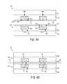
- FIGS. 1A and 1Bare simplified cross-sectional views of semiconductor structures, and are used to illustrate dishing and erosion phenomena that may occur during preparation of bonding surfaces of semiconductor structures for direct bonding processes used to directly bond semiconductor structures together;
- FIGS. 2A through 2Kare simplified cross-sectional views of semiconductor structures and illustrate embodiments of direct bonding processes of the present invention for directly bonding together semiconductor structures;
- FIGS. 3A through 3Kare simplified cross-sectional views of semiconductor structures and illustrate additional embodiments of direct bonding processes of the present invention.
- FIGS. 4A and 4Bare simplified cross-sectional views of semiconductor structures and illustrate yet further embodiments of direct bonding processes of the present invention.
- semiconductor structuremeans and includes any structure that is used in the formation of a semiconductor device.
- Semiconductor structuresinclude, for example, dies and wafers (e.g., carrier substrates, interposers, and device substrates), as well as assemblies or composite structures that include two or more dies, wafers, or combinations thereof that have been three-dimensionally integrated with one another.
- Semiconductor structuresalso include fully fabricated semiconductor devices, as well as intermediate structures formed during fabrication of semiconductor devices.
- processed semiconductor structuremeans and includes any semiconductor structure that includes one or more at least partially formed device structures. Processed semiconductor structures are a subset of semiconductor structures, and all processed semiconductor structures are semiconductor structures.
- bonded semiconductor structuremeans and includes any structure that includes two or more semiconductor structures that are attached together. Bonded semiconductor structures are a subset of semiconductor structures, and all bonded semiconductor structures are semiconductor structures. Furthermore, bonded semiconductor structures that include one or more processed semiconductor structures are also processed semiconductor structures.
- the term “device structure”means and includes any portion of a processed semiconductor structure that is, includes, or defines at least a portion of an active or passive component of a semiconductor device to be formed on or in the semiconductor structure.
- device structuresinclude active and passive components of integrated circuits such as transistors, transducers, capacitors, resistors, conductive lines, conductive vias, and conductive contact pads.
- through wafer interconnectmeans and includes any conductive via extending through at least a portion of a first semiconductor structure that is used to provide a structural and/or an electrical interconnection between the first semiconductor structure and a second semiconductor structure across an interface between the first semiconductor structure and the second semiconductor structure.
- Through wafer interconnectsare also referred to in the art by other terms, such as “through silicon vias,” “through substrate vias,” “through wafer vias,” or abbreviations of such terms, such as “TSVs” or “TWVs.”
- TWIstypically extend through a semiconductor structure in a direction generally perpendicular to the generally flat, major surfaces of the semiconductor structure (i.e., in a direction parallel to the “Z” axis).
- active surfacewhen used in relation to a processed semiconductor structure, means and includes an exposed major surface of the processed semiconductor structure that has been, or will be, processed to form one or more device structures in and/or on the exposed major surface of the processed semiconductor structure.
- back surfacewhen used in relation to a processed semiconductor structure, means and includes an exposed major surface of the processed semiconductor structure on an opposing side of the processed semiconductor structure from an active surface of the semiconductor structure.
- the present inventioncomprises improved methods of directly bonding a first semiconductor structure to a second semiconductor structure to form a bonded semiconductor structure.
- embodiments of the inventionmay comprise forming a bonding surface of a semiconductor structure to have a selected topographical pattern that is purposefully rendered non-planar on the atomic scale to improve a bond to be established between the bonding surface of the semiconductor structure and a bonding surface of another semiconductor structure in a direct bonding process such as an ultra-low temperature bonding process (e.g., a surface-assisted bonding (SAB) process), without using an intermediate adhesive material between the bonding surfaces of the semiconductor structures.
- SABsurface-assisted bonding
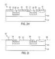
- FIGS. 2A through 2Killustrate the fabrication of a first semiconductor structure 130 shown in FIG. 2D
- FIGS. 2E through 21illustrate the fabrication of a second semiconductor structure 240 shown in FIG. 2I
- FIGS. 2J and 2Killustrate the first semiconductor structure 130 and the second semiconductor structure 240 being bonded together in a direct bonding process to form a bonded semiconductor structure 300 shown in FIG. 2K .
- a semiconductor structure 100is shown, which may be formed as previously described herein with reference to FIGS. 1A and 1B .
- the semiconductor structure 100may comprise a device layer 101 that includes one or more device structures, such as, transistors, vertically extending conductive vias, horizontally extending conductive traces, etc.
- the semiconductor structure 100includes device structures 106 that are defined by and comprise a conductive metal 105 that is disposed within recesses 104 formed or otherwise provided in the dielectric material 102 .
- the conductive material 105may comprise a commercially pure metal element such as copper, aluminum, tungsten, tantalum, titanium, chromium, or a non-metallic conductive material such as doped polysilicon, etc., or the conductive material 105 may comprise an alloy or mixture based on one or more such metal elements.
- the device structures 106may comprise different regions having different compositions.
- the recesses 104may be lined with one or more relatively thin layers of metal to provide, for example, a diffusion barrier layer, a seed layer, etc., and bulk electrically conductive metal, such as copper or a copper alloy, may substantially fill the remaining majority of the volume of the recesses 104 .
- a surface 107 of the device structures 106 that is exposed through the dielectric material 102may, in some embodiments, have a concave shape, which may result from the dishing phenomenon that has been observed upon performing a chemical-mechanical polishing (CMP) process to remove excess conductive material 105 from the semiconductor structure 100 and define the device structures 106 .
- CMPchemical-mechanical polishing
- the surfaces 107 of the device structures 106may be recessed relative to the adjacent surface 103 of the surrounding dielectric material 102 , as shown in FIG. 2A .
- the exposed major surface 103 of the dielectric material 102may not be perfectly planar, and may have pits or recesses at certain locations thereon.
- a concave recess 108is shown in the surface 103 at a location separated from the device structures 106 .
- Such recesses 108also may result from the chemical-mechanical polishing (CMP) process used to remove excess conductive metal 105 from the semiconductor structure 100 and define the device structures 106 , which involves the removal of differing materials and, hence, may be relatively less effective at attaining a planar surface compared to CMP processes that involve the removal of only a single homogeneous material (i.e., CMP processes in which the entire surface being polished has the same composition).
- CMPchemical-mechanical polishing
- a semiconductor structure 110may be formed from the semiconductor structure 100 of FIG. 2A by providing an additional dielectric material 112 over the surface 103 of the dielectric material 102 .
- the additional dielectric material 112may be provided over the dielectric material 102 to an average thickness that fills the recess 108 and the recesses defined by the concave surfaces 107 of the device structures 106 .
- the additional dielectric material 112may be provided over the dielectric material 102 , such that the average distance between the exposed major surface 114 of the additional dielectric material and the surface 103 of the underlying dielectric material 102 is at least about one hundred nanometers (100 nm), at least about five hundred nanometers (500 nm), or even at least about one thousand nanometers (1,000 nm).
- the additional dielectric materialmay comprise, for example, an oxide material such as one or more of silicon oxide, silicon nitride, and silicon oxynitride, and may be deposited using known chemical vapor deposition (CVD) processes.
- the temperature at which the additional dielectric material is depositedmay be selected so as not to damage previously fabricated devices.
- the additional dielectric material 112may be deposited in a conformal manner over the semiconductor structure 100 of FIG. 2A , such that the exposed major surface 114 of the additional dielectric material 112 also includes one or more recesses located over recesses in the underlying surface of the semiconductor structure 100 .
- a recess 116is shown in the exposed major surface 114 of the additional dielectric material 112 that is located over the recess 108 in the underlying surface 103 of the dielectric material 102 .
- additional recessesmay be formed in the exposed major surface 114 of the additional dielectric material 112 at the locations overlying the recessed surfaces 107 of the device structures 106 .
- the exposed major surface 114 of the additional dielectric material 112may be planarized to form another semiconductor structure 120 .
- the exposed major surface 114 of the additional dielectric material 112may be subjected to one or more of a chemical etching process, a mechanical polishing process, or a chemical-mechanical polishing (CMP) process to planarize the exposed major surface 114 of the additional dielectric material 112 .
- CMPchemical-mechanical polishing
- the process used to planarize the exposed major surface 114may involve removal of a portion of the additional dielectric material 112 .
- the original profile of the additional dielectric material 112is shown in FIG. 2C by a phantom line.
- the exposed major surface 114may be at least substantially planar (i.e., smooth). As the planarization process used to planarize the exposed major surface 114 involves planarization of an entire surface having the same composition (i.e., the composition of the additional dielectric material 112 ), the exposed major surface 114 may be smoother after planarization relative to the smoothness of the exposed major surface of the semiconductor structure 100 of FIG. 2A .
- the exposed major surface 114may have a root mean square (RMS) surface roughness of about one-half of a nanometer (0.5 nm) or less, about two tenths of a nanometer (0.2 nm) or less, or even about one tenth of a nanometer (0.1 nm) or less.
- RMSroot mean square
- the semiconductor structure 120 of FIG. 2Cmay be subjected to an etching process to remove the additional dielectric material 112 and a portion of the underlying dielectric material 102 to cause the device structures 106 to project a selected, predetermined distance D 1 from the exposed surface 103 of the dielectric material 102 , as shown in FIG. 2D , and form the previously mentioned first semiconductor structure 130 .
- the distance D 1may be between about one-half of a nanometer (0.5 nm) and about fifty nanometers (50 nm), between about one nanometer (1 nm) and about ten nanometers (10 nm), or even between about two nanometers (2 nm) and about seven nanometers (7 nm).
- the device structures 106 and the dielectric material 102 disposed adjacent the device structures 106are exposed at the bonding surface of the first semiconductor structure 130 .
- the exposed major surface 103 of the dielectric material 102defines a bond plane 132 of the first semiconductor structure.
- the bond plane 132may comprise the plane along which at least a majority of the bonding interface between the first semiconductor structure 130 and the second semiconductor structure 240 ( FIG. 2I ) extends after bonding the first semiconductor structure 130 and the second semiconductor structure 240 together, as discussed in further detail below with reference to FIGS. 2J and 2K .
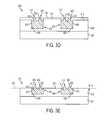
- FIGS. 2E through 2IAn example method that may be used to form the second semiconductor structure 240 of FIG. 2I is now described with reference to FIGS. 2E through 2I .
- a semiconductor structure 200may be provided.
- the semiconductor structure 200may be substantially similar to the semiconductor structure 100 of FIG. 2A , and may include a device layer 201 that includes one or more device structures, such as, transistors, vertically extending conductive vias, horizontally extending conductive traces, etc.
- the semiconductor structure 200includes a dielectric material 202 disposed over the device layer 201 , and device structures 206 that are defined by and comprise a conductive material 205 that is disposed within recesses 204 formed or otherwise provided in the dielectric material 202 .
- the conductive material 205may have a composition as previously described in relation to the conductive material 105 of FIG. 2A .
- a surface 207 of the device structures 206 that is exposed through the dielectric material 202may, in some embodiments, have a concave shape, which may result from the dishing phenomenon that has been observed upon performing a chemical-mechanical polishing (CMP) process to remove excess conductive metal 205 from the semiconductor structure 200 and define the device structures 206 .
- CMPchemical-mechanical polishing
- the surfaces 207 of the device structures 206may be recessed relative to the adjacent surface 203 of the surrounding dielectric material 202 , as shown in FIG. 2E .
- the exposed major surface 203 of the dielectric material 202may not be perfectly planar, and may have pits or recesses at certain locations thereon.
- a concave recess 208is shown in the surface 203 at a location separated from the device structures 206 .
- Such recesses 208also may result from the chemical-mechanical polishing (CMP) process used to remove excess conductive metal 205 from the semiconductor structure 200 and define the device structures 206 , as previously discussed herein.
- CMPchemical-mechanical polishing
- a semiconductor structure 210may be formed from the semiconductor structure 200 of FIG. 2E by providing an additional dielectric material 212 over the surface 203 of the dielectric material 202 .
- the additional dielectric material 212may be provided over the dielectric material 202 to an average thickness that fills the recess 208 and the recesses defined by the concave surfaces 207 of the device structures 206 .
- the additional dielectric material 212may have a composition and configuration (e.g., average thickness) as previously disclosed in relation to the additional dielectric material 112 with reference to FIG. 2B .
- the additional dielectric material 212may be deposited in a conformal manner over the semiconductor structure 200 of FIG. 2E , such that the exposed major surface 214 of the additional dielectric material 212 also includes one or more recesses located over recesses in the underlying surface of the semiconductor structure 200 .
- a recess 216is shown in the exposed major surface 214 of the additional dielectric material 212 that is located over the recess 208 in the underlying surface 203 of the dielectric material 202 .
- additional recessesmay be formed in the exposed major surface 214 of the additional dielectric material 212 at the locations overlying the recessed surfaces 207 of the device structures 206 .
- the exposed major surface 214 of the additional dielectric material 212may be planarized to form another semiconductor structure 220 in a manner like that previously described in relation to the additional dielectric material 112 with reference to FIG. 2C .
- the exposed major surface 214 of the additional dielectric material 212may be subjected to one or more of a chemical etching process, a mechanical polishing process, or a chemical-mechanical polishing (CMP) process to planarize the exposed major surface 214 of the additional dielectric material 212 .
- CMPchemical-mechanical polishing
- the process used to planarize the exposed major surface 214may involve removal of a portion of the additional dielectric material 212 .
- the original profile of the additional dielectric material 212is shown in FIG. 2G by a phantom line.
- the exposed major surface 214may be at least substantially planar (i.e., smooth).
- the exposed major surface 214may be smoother after planarization relative to the smoothness of the exposed major surface of the semiconductor structure 200 of FIG. 2E .
- the exposed major surface 214may have a root mean square (RMS) surface roughness of about one-half of a nanometer (0.5 nm) or less, about two tenths of a nanometer (0.2 nm) or less, or even about one tenth of a nanometer (0.1 nm) or less.
- RMSroot mean square
- a mask material 232may be provided over the planarized exposed major surface 214 .
- the mask material 232may be blanket deposited over at least substantially the entire exposed major surface 214 , and subsequently patterned to form apertures 234 (e.g., holes or other openings) extending through the mask material 232 .
- the apertures 234may be aligned with the device structures 206 , as shown in FIG. 2H . Further, the apertures 234 may have sizes and shapes that correspond to the sizes and shapes of the underlying device structures 206 .
- the patterned mask material 232may be used to facilitate removal of the regions of the additional dielectric material 212 overlying the device structures 206 without removing other regions of the additional dielectric material 212 .
- the mask material 232may comprise, for example, a polymeric photoresist material such as poly(methyl methacrylate) (PMMA), which may be deposited by spinning on a layer of uncured photoresist material, and subsequently subjecting certain selected regions of the uncured photoresist material to electromagnetic radiation through a patterned reticle to cure only selected regions of the uncured photoresist material. Uncured regions of the photoresist material then may be removed to form the patterned mask material 232 as shown in FIG. 2H .
- the mask material 232may comprise a hard mask material, such as silicon nitride (Si 3 N 4 ), and may be deposited using, for example, a chemical vapor deposition (CVD) process.
- Photolithographic techniquesthen may be used to pattern the deposited hard mask material to form the patterned mask material 232 , as shown in FIG. 2H .
- Various mask materials, and methods for depositing and patterning such mask materials,are known in the art and may be employed in embodiments of the invention.
- the regions of the additional dielectric material 212 that are exposed through the apertures 234 in the patterned mask material 232 overlying the device structures 206may be removed to form a semiconductor structure 240 , as shown in FIG. 2I .
- the semiconductor structure 230 of FIG. 2Hmay be exposed to one or more etchants in a wet chemical etching process or a dry reactive ion etching (RIE) process.
- RIEreactive ion etching
- the one or more etchantsmay be selected to have a composition that will etch the additional dielectric material 212 without removing the patterned mask material 232 and device structures 206 , or that will etch the additional dielectric material 212 at a higher rate relative to the rate at which the patterned mask material 232 and device structures 206 are etched by the one or more etchants, such that at least substantially all of the additional dielectric material 212 overlying the device structures 206 may be removed by the one or more etchants without etching entirely through the patterned mask material 232 .
- the patterned mask material 232may be removed, as shown in FIG. 2I .
- the exposed major surface 214 of the additional dielectric material 212may have a root mean square (RMS) surface roughness of about point five tenths of a nanometer (0.5 nm) or less, about two tenths of a nanometer (0.2 nm) or less, or even about one tenth of a nanometer (0.1 nm) or less.
- RMSroot mean square
- the etching process used to remove the regions of the additional dielectric material 212 overlying the device structures 206 that are exposed through the apertures 234 in the patterned mask material 232may cause the exposed surfaces 207 of the device structures 206 to be recessed a selected, predetermined distance D 2 from the exposed surface 214 of the surrounding additional dielectric material 212 , as shown in FIG. 2I .
- an etching process used to remove an oxidemay cause the exposed surfaces 207 of the device structures 206 to have a recessed or dished shape in embodiments in which the device structures comprise polysilicon.
- the device structures 206may be caused to have a recessed or dished shape due to a chemical-mechanical polishing (CMP) process used to remove excess conductive material 205 from the semiconductor structure 200 and define the device structures 206 , as previously described with reference to FIG. 2A .
- CMPchemical-mechanical polishing
- the distance D 2may be between about one tenth of a nanometer (0.1 nm) and about ten nanometers (10 nm), between about one nanometer (1 nm) and about ten nanometers (10 nm), or even between about two nanometers (2 nm) and about seven nanometers (7 nm).
- the distance D 2 of FIG. 2Imay be at least substantially equal to the distance D 1 of FIG. 2D . In additional embodiments, however, the distance D 2 of FIG. 2I may be less than the distance D 1 of FIG. 2D .
- the distance D 2 of FIG. 2Imay be between about 80% and about 99% of the distance D 1 of FIG. 2D , or more particularly, between about 90% and about 98% of the distance D 1 of FIG. 2D .
- the device structures 206 and the additional dielectric material 212 disposed adjacent the device structures 206are exposed at the bonding surface of the second semiconductor structure 240 .
- the exposed major surface 214 of the additional dielectric material 212defines a bond plane 242 of the second semiconductor structure 240 .
- the bond plane 242may comprise the plane along which at least a majority of the bonding interface between the first semiconductor structure 130 ( FIG. 2D ) and the second semiconductor structure 240 extends after bonding the first semiconductor structure 130 and the second semiconductor structure 240 together, as discussed in further detail below with reference to FIGS. 2J and 2K .
- the first semiconductor structure 130may be aligned with the second semiconductor structure 240 such that the device structures 106 of the first semiconductor structure 130 are aligned with the device structures 206 of the second semiconductor structure 240 .
- the exposed surfaces of the device structures 106 and the exposed major surface 103 of the surrounding dielectric material 102together define a bonding surface of the first semiconductor structure 130
- the exposed surfaces of the device structures 206 and the exposed major surface 214 of the surrounding additional dielectric material 212together define a bonding surface of the second semiconductor structure 240 .
- the topography of the bonding surface of the first semiconductor structure 130has a male configuration in which the device structures 106 project from the first semiconductor structure 130
- the topography of the bonding surface of the second semiconductor structure 240has a female configuration in which the device structures 206 are disposed in recesses that extend into the second semiconductor structure 240 .
- the projecting device structures 106 of the first semiconductor structure 130may be inserted into the recesses in which the device structures 206 of the second semiconductor structure 240 are disposed, and the bonding surface of the first semiconductor structure 130 may be abutted against the bonding surface of the second semiconductor structure 240 .
- the device structures 106 of the first semiconductor structure 130may abut directly against corresponding, respective device structures 206 of the second semiconductor structure 240 .
- no intermediate bonding materiale.g., adhesive
- the device structures 106 of the first semiconductor structure 130then may be directly bonded to the device structures 206 of the second semiconductor structure 240 to form the bonded semiconductor structure 300 shown in FIG. 2K .
- the bonding processresults in the formation of bonded conductive structures that include the device structures 106 and the device structures 206 that have been bonded together.
- the device structures 206 of the second semiconductor structure 240may be directly bonded to the device structures 106 of the first semiconductor structure 130 in a direct conductive material-to-conductive material ultra-low temperature direct bonding process carried out in an environment at a temperature or temperatures of about two hundred degrees Celsius (200° C.) or less, or even in an environment at a temperature or temperatures of about one hundred degrees Celsius (100° C.) or less. In some embodiments, such an ultra-low temperature direct bonding process may be carried out at in an environment at about room temperature (i.e., without any applied heat additional to that provided by the ambient environment).
- the first semiconductor structure 130 and the second semiconductor structure 240may be processed to remove surface impurities and undesirable surface compounds.
- the first semiconductor structure 130may be directly bonded to the second semiconductor structure 240 without applying pressure between the bonding surfaces at the bonding interface therebetween.
- pressuremay be applied between the bonding surfaces at the bonding interface in some ultra-low temperature direct bonding methods in order to achieve a suitable bond strength at the bonding interface.
- the direct bonding methods used to bond the device structures 106 of the first semiconductor structure 130 to the device structures 206 of the second semiconductor structure 240may comprise surface assisted bonding (SAB) bonding methods in some embodiments of the invention.
- SABsurface assisted bonding
- a bond interface 302may be identified between the bonded device structures 106 of the first semiconductor structure 130 and the device structures 206 of the second semiconductor structure 240 . Such a bond interface 302 may only be visible under magnification of a prepared cross-section of the bonded semiconductor structure 300 . In some instances, it may not be possible to see the bond interfaces 302 after the bonding process is complete, even with the aid of magnification. However, as shown in FIG.
- the bond interfaces 302 between the bonded device structures 106 of the first semiconductor structure 130 and the device structures 206 of the second semiconductor structure 240may be separated from a primary bonding interface plane 304 between the first semiconductor structure 130 and the second semiconductor structure 240 .
- the primary bonding interface plane 304is defined as the plane along which the major surface 214 of the additional dielectric material 212 of the second semiconductor device 240 abuts against the major surface 103 of the dielectric material 102 of the first semiconductor device 130 .
- the bond interfaces 302may be separated from the primary bonding interface plane 304 by a distance that is at least substantially equal to the distance D 1 of FIG. 2D and/or the distance D 2 of FIG. 2I .
- the distance D 2 of FIG. 2Imay be approximately equal to the distance D 1 of FIG. 2D in some embodiments.
- direct physical contactmay be sufficiently established between the device structures 106 of the first semiconductor structure 130 and the device structures 206 of the second semiconductor structure 240 during the direct bonding process may be enhanced without any problems that might arise by any expansion of the materials during subsequent annealing or other thermal treatment processes, which may improve the bond established therebetween.
- FIGS. 3A through 3Killustrate the fabrication of a first semiconductor structure 450 shown in FIG. 3E
- FIGS. 3F through 31illustrate the fabrication of a second semiconductor structure 570 shown in FIG. 3I
- FIGS. 3J and 3Killustrate the first semiconductor structure 450 and the second semiconductor structure 570 being bonded together in a direct bonding process to form a bonded semiconductor structure 600 shown in FIG. 3K .
- a semiconductor structure 400may be formed by providing a patterned mask material 418 over a semiconductor structure like the semiconductor structure 120 shown in FIG. 2C .
- the semiconductor structure 400is at least substantially similar to the semiconductor structure 120 ( FIG. 2C ), and includes a device layer 401 (comprising one or more device structures, such as, transistors, vertically extending conductive vias, horizontally extending conductive traces, etc.), a dielectric material 402 over the device layer 401 , and device structures 406 that are defined by and comprise a conductive material 405 disposed within recesses 404 formed or otherwise provided in the dielectric material 402 .
- An additional dielectric material 412 having a planarized surface 414may be provided over the dielectric material 402 , such that the additional dielectric material 412 fills any recesses 408 in the major surface 403 of the dielectric material 402 and any recesses defined by concave surfaces 407 of the device structures 406 .
- the patterned mask material 418may be disposed over the major surface 414 of the additional dielectric material 412 .
- the mask material 418may be blanket deposited over at least substantially the entire major surface 414 of the additional dielectric material 412 , and subsequently patterned to form apertures 419 (e.g., holes or other openings) extending through the mask material 418 .
- the apertures 419may be aligned with the device structures 406 , as shown in FIG. 3A .
- the apertures 419may have cross-sectional dimensions small enough to allow two or more apertures 419 to be disposed over and aligned with a single underlying device feature 406 , as shown in FIG. 3A .
- the patterned mask material 418may be used to facilitate removal of some regions of the additional dielectric material 412 overlying the device structures 406 without removing other regions of the additional dielectric material 412 .
- the mask material 418may comprise, for example, a polymeric photoresist material such as poly(methyl methacrylate) (PMMA), which may be deposited by spinning on a layer of uncured photoresist material, and subsequently subjecting certain selected regions of the uncured photoresist material to electromagnetic radiation through a patterned reticle to cure only selected regions of the uncured photoresist material. Uncured regions of the photoresist material then may be removed to form the patterned mask material 418 as shown in FIG. 3A .
- the mask material 418may comprise a hard mask material, such as silicon nitride (Si 3 N 4 ), and may be deposited using, for example, a chemical vapor deposition (CVD) process.
- Photolithographic techniquesthen may be used to pattern the deposited hard mask material to form the patterned mask material 418 , as shown in FIG. 3A .
- Various mask materials, and methods for depositing and patterning such mask materials,are known in the art and may be employed in embodiments of the invention.
- the regions of the additional dielectric material 412 that are exposed through the apertures 419 in the patterned mask material 418 overlying the device structures 406may be removed to form a semiconductor structure 420 , as shown in FIG. 3B .
- the semiconductor structure 400 of FIG. 3Amay be exposed to one or more etchants in a wet chemical etching process or a dry reactive ion etching (RIE) process.
- RIEreactive ion etching
- the one or more etchantsmay be selected to have a composition that will etch the additional dielectric material 412 without removing the patterned mask material 418 and conductive material 405 , or that will etch the additional dielectric material 412 at a higher rate relative to the rate at which the patterned mask material 418 and conductive material 405 is etched by the one or more etchants, such that the regions of the additional dielectric material 412 overlying the device structures 406 that are exposed through the apertures 419 may be removed by the one or more etchants without etching entirely through the patterned mask material 418 .
- the patterned mask material 418may be removed from the semiconductor structure to form the semiconductor structure 420 of FIG. 3B .
- the etching processis used to form a plurality of apertures 422 , each of which extends through the additional dielectric material 412 from the exposed major surface 414 thereof to the surface 407 of the device structures 406 .
- conductive materialmay be provided within the recesses 422 .
- a conductive material 432may be deposited within the recesses 422 to form the semiconductor structure 430 shown therein. In some embodiments, excess conductive material 432 may be deposited, such that a layer of the conductive material 432 covers the major surface 414 of the additional dielectric material 412 , as shown in FIG. 3C .
- the conductive material 432may, in some embodiments, have a composition that is at least substantially the same as the composition of the conductive material 405 of the device structures 406 .
- the conductive material 432may comprise a commercially pure metal element such as copper, aluminum, tungsten, tantalum, titanium, chromium, etc., or the conductive material 432 may comprise an alloy or mixture based on one or more such metal elements, or the conductive material 432 may comprise a conductive semiconductor material (e.g., polysilicon). Further, the conductive material 432 may comprise different regions having different compositions.
- the apertures 422may be lined with one or more relatively thin layers of metal to provide, for example, a diffusion barrier layer, a seed layer, etc., and bulk electrically conductive metal, such as copper or a copper alloy, may be deposited over the one or more relatively thin layers.
- the conductive material 432may be deposited using one or more of an electroless plating process, an electrolytic plating process, a physical deposition process (PVD), and a chemical vapor deposition (CVD) process (including low-pressures CVD or “LPCVD” processes.
- an electroless plating processan electrolytic plating process
- PVDphysical deposition process
- CVDchemical vapor deposition
- the excess conductive material 432 disposed over the major surface 414 of the additional dielectric material 412may be removed using, for example, one or more of a chemical etching process, a mechanical polishing process, or a chemical-mechanical polishing (CMP) process to form the semiconductor structure 440 shown in FIG. 3D .
- the excess conductive material 432may be removed by subjecting the excess conductive material 432 to a chemical-mechanical polishing (CMP) process, which may be carried out at least until the major surface 414 of the additional dielectric material 412 is exposed through the conductive material 432 , as shown in FIG. 3D .
- CMPchemical-mechanical polishing
- each of the device structures 406includes a plurality of integral protrusions 442 defined by the conductive material 432 in the apertures 422 , which integral protrusions 442 extend from a base structure defined by the conductive material 405 in the recesses 404 .
- the chemical-mechanical polishing (CMP) process used to remove the excess conductive material 432may also planarize the exposed major surface 414 of the additional dielectric material 412 .
- At least a portion of the additional dielectric material 412 laterally surrounding the integral protrusions 442may be removed to cause the integral protrusions 442 to project a selected, predetermined distance D 3 from the exposed surface 403 of the dielectric material 402 and/or from the exposed surface 414 of the additional dielectric material 412 , as shown in FIG. 3E , and form the previously mentioned first semiconductor structure 450 .
- the distance D 3may be between about one-half of a nanometer (0.5 nm) and about fifty nanometers (50 nm), between about one nanometer (1 nm) and about ten nanometers (10 nm), or even between about two nanometers (2 nm) and about seven nanometers (7 nm).
- the exposed surfaces of the integral protrusions 442 of the device structures 406 , the exposed major surface 403 of the surrounding dielectric material 402 , and/or the exposed surface 414 of the additional dielectric material 412together define a bonding surface of the first semiconductor structure 450 that will be abutted against and bonded to a complementary bonding surface of the second semiconductor structure 570 shown in FIG. 3I .
- the integral protrusions 442 of the device structures 406 , the dielectric material 402 disposed adjacent the integral protrusions 442 , and the additional dielectric material 412 disposed adjacent the integral protrusions 442are exposed at the bonding surface of the first semiconductor structure 450 . Further, portions of the additional dielectric material 412 are disposed adjacent the device structures 406 and extend over a portion of the device structures 406 between the integral protrusions 442 , as shown in FIG. 3E .
- the exposed major surface 403 of the dielectric material 402 and the exposed major surface 414 of the additional dielectric material 412define a bond plane 452 of the first semiconductor structure 450 .
- the bond plane 452may comprise the plane along which at least a majority of the bonding interface between the first semiconductor structure 450 and the second semiconductor structure 570 ( FIG. 3I ) extends after bonding the first semiconductor structure 450 and the second semiconductor structure 570 together, as discussed in further detail below with reference to FIGS. 3J and 3K .
- FIGS. 3F through 3IAn example method that may be used to form the second semiconductor structure 570 of FIG. 3I is now described with reference to FIGS. 3F through 3I .
- a semiconductor structure 500may be provided that is at least substantially similar to the semiconductor structure 440 of FIG. 3D .
- the semiconductor structure 500may include a device layer 501 that includes one or more device structures, such as, transistors, vertically extending conductive vias, horizontally extending conductive traces, etc.
- the semiconductor structure 500includes a dielectric material 502 disposed over the device layer 501 , and device structures 506 that are at least partially surrounded by the dielectric material 502 .
- the conductive material 505may have a composition as previously described in relation to the conductive material 105 of FIG. 2A .
- the semiconductor structure 500further includes an additional dielectric material 512 disposed over the surface 503 of the dielectric material 502 .
- Each of the device structures 506includes a plurality of integral protrusions 542 that extend from a base structure defined by the conductive material 505 in recesses 504 that extend into the dielectric material 502 .
- the integral protrusions 542are defined by a conductive material 532 disposed in apertures 522 that extend through the additional dielectric material 512 .
- the composition of the conductive material 532may be the same as, or different from, the composition of the conductive material 505 .
- a major surface 514 of the additional dielectric material 512 and the integral protrusions 542 of the device structures 506are exposed on the semiconductor structure 500 .
- a semiconductor structure 550may be formed from the semiconductor structure 500 of FIG. 3F by providing an additional dielectric material 552 over the surface 514 of the additional dielectric material 512 .
- a layer of the additional dielectric material 552may be provided over the additional dielectric material 512 to a desirable average thickness.
- the additional dielectric material 552may have a composition and configuration (e.g., average thickness) as previously disclosed in relation to the additional dielectric material 112 with reference to FIG. 2B .
- the exposed major surface 554 of the additional dielectric material 552optionally may be planarized.
- the exposed major surface 554 of the additional dielectric material 552may be subjected to one or more of a chemical etching process, a mechanical polishing process, or a chemical-mechanical polishing (CMP) process to planarize the exposed major surface 554 of the additional dielectric material 552 .
- CMPchemical-mechanical polishing
- the exposed major surface 554may have a root mean square (RMS) surface roughness of about one-half of a nanometer (0.5 nm) or less, about two tenths of a nanometer (0.2 nm) or less, or even about one tenth of a nanometer (0.1 nm) or less.
- RMSroot mean square
- a patterned mask material 562may be provided over the planarized exposed major surface 554 to form the semiconductor structure 560 shown in FIG. 3H .
- the mask material 562may be blanket deposited over at least substantially the entire exposed major surface 554 , and subsequently patterned to form apertures 564 (e.g., holes or other openings) extending through the mask material 562 .
- the apertures 564may be aligned with the integral protrusions 542 of the device structures 506 , as shown in FIG. 3H .
- the apertures 564may have sizes and shapes that correspond to the sizes and shapes of the underlying integral protrusions 542 of the device structures 506 .
- the patterned mask material 562may be used to facilitate removal of the regions of the additional dielectric material 552 overlying the integral protrusions 542 of the device structures 506 without removing other regions of the additional dielectric material 552 and the device structures 506 .
- the mask material 562may comprise, for example, a polymeric photoresist material such as poly(methyl methacrylate) (PMMA), which may be deposited by spinning on a layer of uncured photoresist material, and subsequently subjecting certain selected regions of the uncured photoresist material to electromagnetic radiation through a patterned reticle to cure only selected regions of the uncured photoresist material. Uncured regions of the photoresist material then may be removed to form the patterned mask material 562 as shown in FIG. 3H .
- the mask material 562may comprise a hard mask material, such as silicon nitride (Si 3 N 4 ), and may be deposited using, for example, a chemical vapor deposition (CVD) process.
- Photolithographic techniquesthen may be used to pattern the deposited hard mask material to form the patterned mask material 562 , as shown in FIG. 3H .
- Various mask materials, and methods for depositing and patterning such mask materials,are known in the art and may be employed in embodiments of the invention.
- the regions of the additional dielectric material 552 that are exposed through the apertures 564 in the patterned mask material 562 overlying the integral protrusions 542 of the device structures 506may be removed, as shown in the semiconductor structure 570 of FIG. 3I .
- the semiconductor structure 560 of FIG. 3Hmay be exposed to one or more etchants in a wet chemical etching process or a dry reactive ion etching (RIE) process.
- RIEreactive ion etching
- the one or more etchantsmay be selected to have a composition that will etch the additional dielectric material 552 without removing the patterned mask material 562 and device structures 506 , or that will etch the additional dielectric material 552 at a higher rate relative to the rate at which the patterned mask material 562 and device structures 506 are etched by the one or more etchants, such that at least substantially all of the additional dielectric material 552 overlying the integral protrusions 542 of the device structures 506 may be removed by the one or more etchants without etching entirely through the patterned mask material 562 .
- the patterned mask material 562may be removed, as shown in FIG. 3I .
- the exposed major surface 554 of the additional dielectric material 552may have a root mean square (RMS) surface roughness of about one-half of a nanometer (0.5 nm) or less, about two tenths of a nanometer (0.2 nm) or less, or even about one tenth of a nanometer (0.1 nm) or less.
- RMSroot mean square
- the etching process used to remove the regions of the additional dielectric material 552 overlying the integral protrusions 542 of the device structures 506 that are exposed through the apertures 564 in the patterned mask material 562may cause the exposed surfaces of the integral protrusions 542 of the device structures 506 to be recessed a selected, predetermined distance D 4 from the exposed surface 554 of the surrounding additional dielectric material 552 , as shown in FIG. 3I .
- apertures 555are formed, each of which extends through the additional dielectric material 552 from the exposed major surface 554 thereof to a surface of the device structures 506 .
- the distance D 4may be between about one-half of a nanometer (0.5 nm) and about fifty nanometers (50 nm), between about one nanometer (1 nm) and about ten nanometers (10 nm), or even between about two nanometers (2 nm) and about seven nanometers (7 nm).
- the distance D 4 of FIG. 3Imay be at least substantially equal to the distance D 3 of FIG. 3E . In additional embodiments, however, the distance D 4 of FIG. 3I may be greater than the distance D 3 of FIG. 3E .
- the distance D 3 of FIG. 3Emay be between about 80% and about 99% of the distance D 4 of FIG. 3I , or more particularly, between about 90% and about 98% of the distance D 4 of FIG. 3I .
- the integral protrusions 542 of the device structures 506 and the additional dielectric material 552are exposed at the bonding surface of the second semiconductor structure 570 .
- the exposed major surface 554 of the additional dielectric material 552defines a bond plane 572 of the second semiconductor structure 570 .
- the bond plane 572may comprise the plane along which at least a majority of the bonding interface between the first semiconductor structure 450 ( FIG. 3E ) and the second semiconductor structure 570 extends after bonding the first semiconductor structure 450 and the second semiconductor structure 570 together, as discussed in further detail below with reference to FIGS. 3J and 3K .
- the first semiconductor structure 450may be aligned with the second semiconductor structure 570 such that the integral protrusions 442 of the device structures 406 of the first semiconductor structure 450 are aligned with the integral protrusions 542 of the device structures 506 of the second semiconductor structure 570 .
- the exposed surfaces of the integral protrusions 442 of the device structures 406 and the exposed major surface 403 of the surrounding dielectric material 402together define a bonding surface of the first semiconductor structure 450
- the exposed surfaces of the integral protrusions 542 of the device structures 506 and the exposed major surface 554 of the surrounding additional dielectric material 552together define a bonding surface of the second semiconductor structure 570 .
- the topography of the bonding surface of the first semiconductor structure 450has a male configuration in which the integral protrusions 442 of the device structures 406 project from the first semiconductor structure 450
- the topography of the bonding surface of the second semiconductor structure 570has a female configuration in which the integral protrusions 542 of the device structures 506 are disposed in recesses that extend into the second semiconductor structure 570 .
- the projecting integral protrusions 442 of the device structures 406 of the first semiconductor structure 450may be inserted into the recesses in which the integral protrusions 542 of the device structures 506 of the second semiconductor structure 570 are disposed, and the bonding surface of the first semiconductor structure 450 may be abutted against the bonding surface of the second semiconductor structure 570 .
- the integral protrusions 442 of the device structures 406 of the first semiconductor structure 450may abut directly against corresponding, respective integral protrusions 542 of the device structures 506 of the second semiconductor structure 570 .
- no intermediate bonding materiale.g., adhesive
- adhesivemay be provided between the abutting integral protrusions 442 of the device structures 406 of the first semiconductor structure 450 and the integral protrusions 542 of the device structures 506 of the second semiconductor structure 570 .
- the integral protrusions 442 of the device structures 406 of the first semiconductor structure 450then may be directly bonded to the integral protrusions 542 of the device structures 506 of the second semiconductor structure 570 to form the bonded semiconductor structure 600 shown in FIG. 3K .
- the bonding processresults in the formation of bonded conductive structures that include the device structures 406 and the device structures 506 that have been bonded together.
- the integral protrusions 542 of the device structures 506 of the second semiconductor structure 570may be directly bonded to the integral protrusions 442 of the device structures 406 of the first semiconductor structure 450 in a direct conductive material-to-conductive material ultra-low temperature direct bonding process carried out in an environment at a temperature or temperatures of about two hundred degrees Celsius (200° C.) or less, or even in an environment at a temperature or temperatures of about one hundred degrees Celsius (100° C.) or less. In some embodiments, such an ultra-low temperature direct bonding process may be carried out at in an environment at about room temperature (i.e., without any applied heat additional to that provided by the ambient environment).
- the first semiconductor structure 450 and the second semiconductor structure 570may be processed to remove surface impurities and undesirable surface compounds.
- the first semiconductor structure 450may be directly bonded to the second semiconductor structure 570 without applying pressure between the bonding surfaces at the bonding interface therebetween.
- pressuremay be applied between the bonding surfaces at the bonding interface in some ultra-low temperature direct bonding methods in order to achieve a suitable bond strength at the bonding interface.
- the direct bonding methods used to bond the integral protrusions 442 of the device structures 406 of the first semiconductor structure 450 to the integral protrusions 542 of the device structures 506 of the second semiconductor structure 570may comprise surface assisted bonding (SAB) bonding methods in some embodiments of the invention.
- SABsurface assisted bonding
- a bond interface 602may be identified between the bonded integral protrusions 442 of the device structures 406 of the first semiconductor structure 450 and the integral protrusions 542 of the device structures 506 of the second semiconductor structure 570 .
- Such a bond interface 602may only be visible under magnification of a prepared cross-section of the bonded semiconductor structure 600 . In some instances, it may not be possible to see the bond interfaces 602 after the bonding process is complete, even with the aid of magnification. However, as shown in FIG.
- the bond interfaces 602 between the bonded integral protrusions 442 of the device structures 406 of the first semiconductor structure 450 and the integral protrusions 542 of the device structures 506 of the second semiconductor structure 570may be separated from a primary bonding interface plane 604 between the first semiconductor structure 450 and the second semiconductor structure 570 .
- the primary bonding interface plane 604is defined as the plane along which the major surface 554 of the dielectric material 552 of the second semiconductor device 570 abuts against the major surface 403 of the dielectric material 402 of the first semiconductor device 450 .
- the bond interfaces 602may be separated from the primary bonding interface plane 604 by a distance that is at least substantially equal to the distance D 3 of FIG. 3E and/or the distance D 4 of FIG. 3I .
- the bonded interface between the directly bonded conductive device structures of the first and second semiconductor structuresmay be at least substantially coplanar with the primary bonding interface between the first and second semiconductor structures.
- FIGS. 4A and 4Billustrate the direct bonding of a first semiconductor structure 440 as previously described in relation to FIG. 3D and a second semiconductor structure 500 as previously described in relation to FIG. 3F (which may, in some embodiments, be at least substantially similar to the first semiconductor structure 440 ) to form a bonded semiconductor structure 700 shown in FIG. 4B .
- the first semiconductor structure 440may be aligned with the second semiconductor structure 500 such that the integral protrusions 442 of the device structures 406 of the first semiconductor structure 440 are aligned with the integral protrusions 542 of the device structures 506 of the second semiconductor structure 500 .
- the exposed surfaces of the integral protrusions 442 of the device structures 406 and the exposed major surface 414 of the surrounding additional dielectric material 412together define an at least substantially planar bonding surface of the first semiconductor structure 440
- the exposed surfaces of the integral protrusions 542 of the device structures 506 and the exposed major surface 514 of the surrounding additional dielectric material 512together define an at least substantially planar bonding surface of the second semiconductor structure 500 .
- the bonding surface of the first semiconductor structure 440may be abutted against the bonding surface of the second semiconductor structure 500 such that the integral protrusions 442 of the device structures 406 of the first semiconductor structure 440 are abutted directly against and in direct physical contact with the integral protrusions 542 of the device structures 506 of the second semiconductor structure 500 without any intermediate bonding material (e.g., adhesive) therebetween.
- intermediate bonding materiale.g., adhesive
- the integral protrusions 442 of the device structures 406 of the first semiconductor structure 440then may be directly bonded to the integral protrusions 542 of the device structures 506 of the second semiconductor structure 500 to form the bonded semiconductor structure 700 shown in FIG. 4B .
- the bonding processmay be carried out as previously described with reference to FIGS. 2K and 3K .
- the bond interfaces 702 between the bonded integral protrusions 442 of the device structures 406 of the first semiconductor structure 440 and the integral protrusions 542 of the device structures 506 of the second semiconductor structure 500may be at least substantially coplanar with a primary bonding interface plane 704 between the first semiconductor structure 440 and the second semiconductor structure 500 , as shown in FIG. 4B .
- the primary bonding interface plane 704is defined as the plane along which the major surface 514 of the dielectric material 512 of the second semiconductor device 500 abuts against the major surface 414 of the dielectric material 412 of the first semiconductor device 440 .
- Embodiment 1A method of directly bonding a first semiconductor structure to a second semiconductor structure, comprising: providing a first semiconductor structure comprising: at least one device structure comprising a conductive material, the at least one device structure exposed at a bonding surface of the first semiconductor structure; and a dielectric material exposed at the bonding surface of the first semiconductor structure, the dielectric material disposed adjacent the at least one device structure of the first semiconductor structure, an exposed surface of the dielectric material at the bonding surface of the first semiconductor structure defining a bond plane of the first semiconductor structure; causing the at least one device structure of the first semiconductor structure to project a distance from the bond plane of the first semiconductor structure beyond the adjacent dielectric material; providing a second semiconductor structure comprising: at least one device structure comprising a conductive material, the at least one device structure exposed at a bonding surface of the second semiconductor structure; and a dielectric material exposed at the bonding surface of the second semiconductor structure, the dielectric material disposed adjacent the at least one device structure of the second semiconductor structure, an exposed surface of the dielectric material
- Embodiment 2The method of Embodiment 1, wherein causing the at least one device structure of the first semiconductor structure to project the distance from the bond plane of the first semiconductor structure beyond the adjacent dielectric material comprises removing a portion of the dielectric material from the first semiconductor structure.
- Embodiment 3The method of Embodiment 2, wherein removing the portion of the dielectric material from the first semiconductor structure comprises etching the dielectric material.
- Embodiment 4The method of any one of Embodiments 1 through 3, wherein causing the at least one device structure of the first semiconductor structure to project a distance from the bond plane of the first semiconductor structure comprises causing the at least one device structure of the first semiconductor structure to project a selected, predetermined distance from the bond plane of the first semiconductor structure.
- Embodiment 5The method of any one of Embodiments 1 through 4, further comprising causing the at least one device structure of the second semiconductor structure to be recessed a distance from the bond plane of the second semiconductor structure into a recess extending into the adjacent dielectric material.
- Embodiment 6The method of Embodiment 5, wherein causing the at least one device structure of the second semiconductor structure to be recessed the distance from the bond plane of the second semiconductor structure into the recess extending into the adjacent dielectric material comprises: depositing dielectric material over the at least one device structure of the second semiconductor structure; and etching through the dielectric material to the at least one device structure.
- Embodiment 7The method of Embodiment 5 or Embodiment 6, wherein causing the at least one device structure of the second semiconductor structure to be recessed the distance from the bond plane of the second semiconductor structure into the recess extending into the adjacent dielectric material comprises causing the at least one device structure of the second semiconductor structure to be recessed a selected, predetermined distance from the bond plane of the second semiconductor structure.
- Embodiment 8The method of any one of Embodiments 5 through 7, wherein bonding the at least one device structure of the first semiconductor structure directly to the at least one device structure of the second semiconductor structure comprises inserting the at least one device structure of the first semiconductor structure into the recess in the dielectric material of the second semiconductor structure.
- Embodiment 9The method of any one of Embodiments 1 through 8, further comprising forming the at least one device structure of the first semiconductor structure to comprise a plurality of integral protrusions, each integral protrusion of the plurality of integral protrusions projecting the distance from the bond plane of the first semiconductor structure beyond the adjacent dielectric material.
- Embodiment 10The method of Embodiment 9, further comprising: providing dielectric material over the at least one device structure of the second semiconductor structure; and etching through the dielectric material to form a plurality of recesses extending through the dielectric material to the at least one device structure of the second semiconductor structure.
- Embodiment 11The method of Embodiment 10, wherein bonding the at least one device structure of the first semiconductor structure directly to the at least one device structure of the second semiconductor structure comprises inserting each integral protrusion of the plurality of integral protrusions of the at least one device structure of the first semiconductor structure into a corresponding complementary recess of the plurality of recesses extending through the dielectric material to the at least one device structure of the second semiconductor structure.
- Embodiment 12The method of any one of Embodiments 1 through 11, wherein bonding the at least one device structure of the first semiconductor structure directly to the at least one device structure of the second semiconductor structure in a conductive material-to-conductive material direct bonding process comprises bonding the at least one device structure of the first semiconductor structure directly to the at least one device structure of the second semiconductor structure in a non thermo-compression direct bonding process.
- Embodiment 13The method of any one of Embodiments 1 through 12, wherein bonding the at least one device structure of the first semiconductor structure directly to the at least one device structure of the second semiconductor structure in a conductive material-to-conductive material direct bonding process comprises bonding the at least one device structure of the first semiconductor structure directly to the at least one device structure of the second semiconductor structure in an ultra-low temperature direct bonding process.
- Embodiment 14The method of any one of Embodiments 1 through 13, wherein bonding the at least one device structure of the first semiconductor structure directly to the at least one device structure of the second semiconductor structure in a conductive material-to-conductive material direct bonding process comprises bonding the at least one device structure of the first semiconductor structure directly to the at least one device structure of the second semiconductor structure in a surface-assisted direct bonding process.
- Embodiment 15A method of directly bonding a first semiconductor structure to a second semiconductor structure, comprising: providing a first semiconductor structure comprising: at least one device structure comprising a conductive material, the at least one device structure comprising a plurality of integral protrusions extending from a base structure, the plurality of integral protrusions exposed at a bonding surface of the first semiconductor structure; and a dielectric material exposed at the bonding surface of the first semiconductor structure, the dielectric material disposed adjacent the at least one device structure of the first semiconductor structure and extending over a portion of the at least one device structure between the integral protrusions of the plurality of integral protrusions of the at least one device structure of the first semiconductor structure, an exposed surface of the dielectric material at the bonding surface of the first semiconductor structure defining a bond plane of the first semiconductor structure; providing a second semiconductor structure comprising: at least one device structure comprising a conductive material, the at least one device structure comprising a plurality of integral protrusions extending from a base structure,
- Embodiment 16The method of Embodiment 15, wherein providing the first semiconductor structure comprises forming the plurality of integral protrusions extending from the base structure of the at least one device structure of the first semiconductor structure, forming the plurality of integral protrusions comprising: providing the dielectric material over the base structure of the at least one device structure of the first semiconductor structure; etching through the dielectric material to form a plurality of recesses extending through the dielectric material to the base structure of the at least one device structure of the first semiconductor structure; and providing the conductive material in the plurality of recesses to form the plurality of integral protrusions extending from the base structure of the at least one device structure of the first semiconductor structure.
- Embodiment 17The method of Embodiment 15 or Embodiment 16, wherein bonding the plurality of integral protrusions of the at least one device structure of the first semiconductor structure directly to the plurality of integral protrusions of the at least one device structure of the second semiconductor structure in a conductive material-to-conductive material direct bonding process comprises bonding the plurality of integral protrusions of the at least one device structure of the first semiconductor structure directly to the plurality of integral protrusions of the at least one device structure of the second semiconductor structure in at least one of an ultra-low temperature direct bonding process and a surface-assisted direct bonding process.
- Embodiment 18A bonded semiconductor structure, comprising: a first semiconductor structure, comprising: at least one conductive device structure at a bonding surface of the first semiconductor structure; and a dielectric material disposed adjacent the at least one conductive device structure at the bonding surface of the first semiconductor structure; a second semiconductor structure, comprising: at least one conductive device structure at a bonding surface of the second semiconductor structure, the at least one conductive device structure of the second semiconductor structure directly bonded to the at least one conductive device structure of the first semiconductor structure along a bonding interface therebetween; and a dielectric material disposed adjacent the at least one conductive device structure at the bonding surface of the second semiconductor structure, the dielectric material of the second semiconductor structure abutting the dielectric material of the first semiconductor structure along a bond plane; wherein the bonding interface between the at least one conductive device structure of the first semiconductor structure and the at least one conductive device structure of the second semiconductor structure is separated from the bond plane by a distance.
- Embodiment 19The bonded semiconductor structure of Embodiment 18, wherein each of the at least one conductive device structure of the first semiconductor structure and the at least one conductive device structure of the second semiconductor structure is at least substantially comprised of copper or a copper alloy.
- Embodiment 20The bonded semiconductor structure of Embodiment 18 or Embodiment 19, wherein the at least one conductive device structure of the first semiconductor structure comprises a plurality of integral protrusions extending from a base structure.
- Embodiment 21The bonded semiconductor structure of Embodiment 20, wherein the plurality of integral protrusions of the at least one conductive device structure of the first semiconductor structure extend through a plurality of recesses in the dielectric material of the second semiconductor structure.
- Embodiment 22The bonded semiconductor structure of Embodiment 21, wherein the at least one conductive device structure of the second semiconductor structure comprises a plurality of integral protrusions extending from a base structure, the plurality of integral protrusions of the at least one conductive device structure of the second semiconductor structure directly bonded to the integral protrusions of the at least one conductive device structure of the first semiconductor structure.
- Embodiment 23A bonded semiconductor structure, comprising: a first semiconductor structure, comprising: at least one conductive device structure at a bonding surface of the first semiconductor structure, the at least one conductive device structure comprising a plurality of integral protrusions extending from a base structure; and a dielectric material disposed adjacent the at least one conductive device structure at the bonding surface of the first semiconductor structure, at least a portion of the dielectric material disposed between the integral protrusions of the at least one conductive device structure of the first semiconductor structure; a second semiconductor structure, comprising: at least one conductive device structure at a bonding surface of the second semiconductor structure, the at least one conductive device structure comprising a plurality of integral protrusions extending from a base structure; and a dielectric material disposed adjacent the at least one conductive device structure at the bonding surface of the second semiconductor structure, at least a portion of the dielectric material disposed between the integral protrusions of the at least one conductive device structure of the second semiconductor structure, the dielectric material
- Embodiment 24The bonded semiconductor structure of Embodiment 23, wherein the bonded interfaces between the integral protrusions of the at least one conductive device structure of the first semiconductor structure and the integral protrusions of the at least one conductive device structure of the second semiconductor structure are separated from the bond plane.
- Embodiment 25The bonded semiconductor structure of Embodiment 23, wherein the bonded interfaces between the integral protrusions of the at least one conductive device structure of the first semiconductor structure and the integral protrusions of the at least one conductive device structure of the second semiconductor structure are at least substantially coplanar with the bond plane.
Landscapes
- Engineering & Computer Science (AREA)
- Computer Hardware Design (AREA)
- Microelectronics & Electronic Packaging (AREA)
- Power Engineering (AREA)
- Manufacturing & Machinery (AREA)
- Physics & Mathematics (AREA)
- Condensed Matter Physics & Semiconductors (AREA)
- General Physics & Mathematics (AREA)
- Internal Circuitry In Semiconductor Integrated Circuit Devices (AREA)
Abstract
Description
Claims (13)
Priority Applications (4)
| Application Number | Priority Date | Filing Date | Title |
|---|---|---|---|
| US13/185,044US8697493B2 (en) | 2011-07-18 | 2011-07-18 | Bonding surfaces for direct bonding of semiconductor structures |
| TW101120333ATWI493690B (en) | 2011-07-18 | 2012-06-06 | Improved bonding surfaces for direct bonding of semiconductor structures |
| KR1020120078214AKR101401584B1 (en) | 2011-07-18 | 2012-07-18 | Improved bonding surfaces for direct bonding of semiconductor structures |
| CN201210249557.XACN102891091B (en) | 2011-07-18 | 2012-07-18 | For the composition surface of the improvement of direct bond semiconductor structure |
Applications Claiming Priority (1)
| Application Number | Priority Date | Filing Date | Title |
|---|---|---|---|
| US13/185,044US8697493B2 (en) | 2011-07-18 | 2011-07-18 | Bonding surfaces for direct bonding of semiconductor structures |
Publications (2)
| Publication Number | Publication Date |
|---|---|
| US20130020704A1 US20130020704A1 (en) | 2013-01-24 |
| US8697493B2true US8697493B2 (en) | 2014-04-15 |
Family
ID=47555228
Family Applications (1)
| Application Number | Title | Priority Date | Filing Date |
|---|---|---|---|
| US13/185,044Expired - Fee RelatedUS8697493B2 (en) | 2011-07-18 | 2011-07-18 | Bonding surfaces for direct bonding of semiconductor structures |
Country Status (1)
| Country | Link |
|---|---|
| US (1) | US8697493B2 (en) |
Cited By (99)
| Publication number | Priority date | Publication date | Assignee | Title |
|---|---|---|---|---|
| US9653623B2 (en) | 2014-12-02 | 2017-05-16 | Samsung Electronics Co., Ltd. | Methods of manufacturing a semiconductor device |
| US10508030B2 (en) | 2017-03-21 | 2019-12-17 | Invensas Bonding Technologies, Inc. | Seal for microelectronic assembly |
| US10515913B2 (en) | 2017-03-17 | 2019-12-24 | Invensas Bonding Technologies, Inc. | Multi-metal contact structure |
| US10515925B2 (en) | 2017-04-21 | 2019-12-24 | Invensas Bonding Technologies, Inc. | Die processing |
| US10522499B2 (en) | 2017-02-09 | 2019-12-31 | Invensas Bonding Technologies, Inc. | Bonded structures |
| US10529634B2 (en) | 2017-05-11 | 2020-01-07 | Invensas Bonding Technologies, Inc. | Probe methodology for ultrafine pitch interconnects |
| US10546832B2 (en) | 2016-12-21 | 2020-01-28 | Invensas Bonding Technologies, Inc. | Bonded structures |
| US10607937B2 (en) | 2015-12-18 | 2020-03-31 | Invensas Bonding Technologies, Inc. | Increased contact alignment tolerance for direct bonding |
| US10658313B2 (en) | 2017-12-11 | 2020-05-19 | Invensas Bonding Technologies, Inc. | Selective recess |
| US10727219B2 (en) | 2018-02-15 | 2020-07-28 | Invensas Bonding Technologies, Inc. | Techniques for processing devices |
| US10777533B2 (en) | 2012-08-30 | 2020-09-15 | Invensas Bonding Technologies, Inc. | Heterogeneous device |
| US10784191B2 (en) | 2017-03-31 | 2020-09-22 | Invensas Bonding Technologies, Inc. | Interface structures and methods for forming same |
| US10790262B2 (en) | 2018-04-11 | 2020-09-29 | Invensas Bonding Technologies, Inc. | Low temperature bonded structures |
| US10796936B2 (en) | 2016-12-22 | 2020-10-06 | Invensas Bonding Technologies, Inc. | Die tray with channels |
| US10840205B2 (en) | 2017-09-24 | 2020-11-17 | Invensas Bonding Technologies, Inc. | Chemical mechanical polishing for hybrid bonding |
| US10879212B2 (en) | 2017-05-11 | 2020-12-29 | Invensas Bonding Technologies, Inc. | Processed stacked dies |
| US10879226B2 (en) | 2016-05-19 | 2020-12-29 | Invensas Bonding Technologies, Inc. | Stacked dies and methods for forming bonded structures |
| US10896902B2 (en) | 2016-01-13 | 2021-01-19 | Invensas Bonding Technologies, Inc. | Systems and methods for efficient transfer of semiconductor elements |
| US10923408B2 (en) | 2017-12-22 | 2021-02-16 | Invensas Bonding Technologies, Inc. | Cavity packages |
| US10964664B2 (en) | 2018-04-20 | 2021-03-30 | Invensas Bonding Technologies, Inc. | DBI to Si bonding for simplified handle wafer |
| US10998265B2 (en) | 2016-09-30 | 2021-05-04 | Invensas Bonding Technologies, Inc. | Interface structures and methods for forming same |
| US10998292B2 (en) | 2018-06-13 | 2021-05-04 | Invensas Bonding Technologies, Inc. | Offset pads over TSV |
| US11004757B2 (en) | 2018-05-14 | 2021-05-11 | Invensas Bonding Technologies, Inc. | Bonded structures |
| US11011503B2 (en) | 2017-12-15 | 2021-05-18 | Invensas Bonding Technologies, Inc. | Direct-bonded optoelectronic interconnect for high-density integrated photonics |
| US11011418B2 (en) | 2005-08-11 | 2021-05-18 | Invensas Bonding Technologies, Inc. | 3D IC method and device |
| US11011494B2 (en) | 2018-08-31 | 2021-05-18 | Invensas Bonding Technologies, Inc. | Layer structures for making direct metal-to-metal bonds at low temperatures in microelectronics |
| US11031285B2 (en) | 2017-10-06 | 2021-06-08 | Invensas Bonding Technologies, Inc. | Diffusion barrier collar for interconnects |
| US11056348B2 (en) | 2018-04-05 | 2021-07-06 | Invensas Bonding Technologies, Inc. | Bonding surfaces for microelectronics |
| US11056390B2 (en) | 2015-06-24 | 2021-07-06 | Invensas Corporation | Structures and methods for reliable packages |
| US11094653B2 (en)* | 2019-11-13 | 2021-08-17 | Sandisk Technologies Llc | Bonded assembly containing a dielectric bonding pattern definition layer and methods of forming the same |
| US11158606B2 (en) | 2018-07-06 | 2021-10-26 | Invensas Bonding Technologies, Inc. | Molded direct bonded and interconnected stack |
| US11158573B2 (en)* | 2018-10-22 | 2021-10-26 | Invensas Bonding Technologies, Inc. | Interconnect structures |
| US11171117B2 (en) | 2018-06-12 | 2021-11-09 | Invensas Bonding Technologies, Inc. | Interlayer connection of stacked microelectronic components |
| US11169326B2 (en) | 2018-02-26 | 2021-11-09 | Invensas Bonding Technologies, Inc. | Integrated optical waveguides, direct-bonded waveguide interface joints, optical routing and interconnects |
| US11195748B2 (en) | 2017-09-27 | 2021-12-07 | Invensas Corporation | Interconnect structures and methods for forming same |
| US11205600B2 (en) | 2014-03-12 | 2021-12-21 | Invensas Corporation | Integrated circuits protected by substrates with cavities, and methods of manufacture |
| US11205625B2 (en) | 2019-04-12 | 2021-12-21 | Invensas Bonding Technologies, Inc. | Wafer-level bonding of obstructive elements |
| US11244916B2 (en) | 2018-04-11 | 2022-02-08 | Invensas Bonding Technologies, Inc. | Low temperature bonded structures |
| US11244920B2 (en) | 2018-12-18 | 2022-02-08 | Invensas Bonding Technologies, Inc. | Method and structures for low temperature device bonding |
| US11256004B2 (en) | 2018-03-20 | 2022-02-22 | Invensas Bonding Technologies, Inc. | Direct-bonded lamination for improved image clarity in optical devices |
| US11264345B2 (en) | 2015-08-25 | 2022-03-01 | Invensas Bonding Technologies, Inc. | Conductive barrier direct hybrid bonding |
| US20220068890A1 (en)* | 2016-10-07 | 2022-03-03 | Xcelsis Corporation | 3d processor |
| US11276676B2 (en) | 2018-05-15 | 2022-03-15 | Invensas Bonding Technologies, Inc. | Stacked devices and methods of fabrication |
| US11296053B2 (en) | 2019-06-26 | 2022-04-05 | Invensas Bonding Technologies, Inc. | Direct bonded stack structures for increased reliability and improved yield in microelectronics |
| US11296044B2 (en) | 2018-08-29 | 2022-04-05 | Invensas Bonding Technologies, Inc. | Bond enhancement structure in microelectronics for trapping contaminants during direct-bonding processes |
| US11348801B2 (en) | 2016-12-28 | 2022-05-31 | Invensas Bonding Technologies, Inc. | Processing stacked substrates |
| US11355404B2 (en) | 2019-04-22 | 2022-06-07 | Invensas Bonding Technologies, Inc. | Mitigating surface damage of probe pads in preparation for direct bonding of a substrate |
| US11367652B2 (en) | 2016-12-28 | 2022-06-21 | Invensas Bonding Technologies, Inc. | Microelectronic assembly from processed substrate |
| US11373963B2 (en) | 2019-04-12 | 2022-06-28 | Invensas Bonding Technologies, Inc. | Protective elements for bonded structures |
| US11380597B2 (en) | 2017-12-22 | 2022-07-05 | Invensas Bonding Technologies, Inc. | Bonded structures |
| US11385278B2 (en) | 2019-05-23 | 2022-07-12 | Invensas Bonding Technologies, Inc. | Security circuitry for bonded structures |
| US11387214B2 (en) | 2017-06-15 | 2022-07-12 | Invensas Llc | Multi-chip modules formed using wafer-level processing of a reconstituted wafer |
| US11393779B2 (en) | 2018-06-13 | 2022-07-19 | Invensas Bonding Technologies, Inc. | Large metal pads over TSV |
| US11462419B2 (en) | 2018-07-06 | 2022-10-04 | Invensas Bonding Technologies, Inc. | Microelectronic assemblies |
| US11476213B2 (en) | 2019-01-14 | 2022-10-18 | Invensas Bonding Technologies, Inc. | Bonded structures without intervening adhesive |
| US11515291B2 (en) | 2018-08-28 | 2022-11-29 | Adeia Semiconductor Inc. | Integrated voltage regulator and passive components |
| US11538781B2 (en) | 2020-06-30 | 2022-12-27 | Adeia Semiconductor Bonding Technologies Inc. | Integrated device packages including bonded structures |
| US11610846B2 (en) | 2019-04-12 | 2023-03-21 | Adeia Semiconductor Bonding Technologies Inc. | Protective elements for bonded structures including an obstructive element |
| US11621246B2 (en) | 2019-03-29 | 2023-04-04 | Adeia Semiconductor Technologies Llc | Diffused bitline replacement in stacked wafer memory |
| US11626363B2 (en) | 2016-12-29 | 2023-04-11 | Adeia Semiconductor Bonding Technologies Inc. | Bonded structures with integrated passive component |
| US11664357B2 (en) | 2018-07-03 | 2023-05-30 | Adeia Semiconductor Bonding Technologies Inc. | Techniques for joining dissimilar materials in microelectronics |
| US11710718B2 (en) | 2015-07-10 | 2023-07-25 | Adeia Semiconductor Technologies Llc | Structures and methods for low temperature bonding using nanoparticles |
| US11715730B2 (en) | 2017-03-16 | 2023-08-01 | Adeia Semiconductor Technologies Llc | Direct-bonded LED arrays including optical elements configured to transmit optical signals from LED elements |
| US11721653B2 (en) | 2019-12-23 | 2023-08-08 | Adeia Semiconductor Bonding Technologies Inc. | Circuitry for electrical redundancy in bonded structures |
| US11728273B2 (en) | 2020-09-04 | 2023-08-15 | Adeia Semiconductor Bonding Technologies Inc. | Bonded structure with interconnect structure |
| US11735523B2 (en) | 2020-05-19 | 2023-08-22 | Adeia Semiconductor Bonding Technologies Inc. | Laterally unconfined structure |
| US11742314B2 (en) | 2020-03-31 | 2023-08-29 | Adeia Semiconductor Bonding Technologies Inc. | Reliable hybrid bonded apparatus |
| US11760059B2 (en) | 2003-05-19 | 2023-09-19 | Adeia Semiconductor Bonding Technologies Inc. | Method of room temperature covalent bonding |
| US11762200B2 (en) | 2019-12-17 | 2023-09-19 | Adeia Semiconductor Bonding Technologies Inc. | Bonded optical devices |
| US11764177B2 (en) | 2020-09-04 | 2023-09-19 | Adeia Semiconductor Bonding Technologies Inc. | Bonded structure with interconnect structure |
| US20230361067A1 (en)* | 2022-05-03 | 2023-11-09 | United Microelectronics Corp. | Semiconductor structure and manufacturing method thereof |
| US11817424B2 (en) | 2020-07-30 | 2023-11-14 | Samsung Electronics Co., Ltd. | Semiconductor package |
| US11842894B2 (en) | 2019-12-23 | 2023-12-12 | Adeia Semiconductor Bonding Technologies Inc. | Electrical redundancy for bonded structures |
| US11862604B2 (en) | 2018-06-22 | 2024-01-02 | Adeia Semiconductor Inc. | Systems and methods for releveled bump planes for chiplets |
| US11862602B2 (en) | 2019-11-07 | 2024-01-02 | Adeia Semiconductor Technologies Llc | Scalable architecture for reduced cycles across SOC |
| US11876076B2 (en) | 2019-12-20 | 2024-01-16 | Adeia Semiconductor Technologies Llc | Apparatus for non-volatile random access memory stacks |
| US11881454B2 (en) | 2016-10-07 | 2024-01-23 | Adeia Semiconductor Inc. | Stacked IC structure with orthogonal interconnect layers |
| US11901281B2 (en) | 2019-03-11 | 2024-02-13 | Adeia Semiconductor Bonding Technologies Inc. | Bonded structures with integrated passive component |
| US11908739B2 (en) | 2017-06-05 | 2024-02-20 | Adeia Semiconductor Technologies Llc | Flat metal features for microelectronics applications |
| US11929347B2 (en) | 2020-10-20 | 2024-03-12 | Adeia Semiconductor Technologies Llc | Mixed exposure for large die |
| WO2024054803A1 (en)* | 2022-09-07 | 2024-03-14 | Adeia Semiconductor Bonding Technologies Inc. | Bonded structure and method of forming same |
| US11935907B2 (en) | 2014-12-11 | 2024-03-19 | Adeia Semiconductor Technologies Llc | Image sensor device |
| US11955449B2 (en) | 2019-10-23 | 2024-04-09 | Samsung Electronics Co, Ltd. | Stacked semiconductor package |
| US11973056B2 (en) | 2016-10-27 | 2024-04-30 | Adeia Semiconductor Technologies Llc | Methods for low temperature bonding using nanoparticles |
| US12009338B2 (en) | 2020-03-19 | 2024-06-11 | Adeia Semiconductor Bonding Technologies Inc. | Dimension compensation control for directly bonded structures |
| US12074092B2 (en) | 2018-05-30 | 2024-08-27 | Adeia Semiconductor Inc. | Hard IP blocks with physically bidirectional passageways |
| US12080672B2 (en)* | 2019-09-26 | 2024-09-03 | Adeia Semiconductor Bonding Technologies Inc. | Direct gang bonding methods including directly bonding first element to second element to form bonded structure without adhesive |
| US12113054B2 (en) | 2019-10-21 | 2024-10-08 | Adeia Semiconductor Technologies Llc | Non-volatile dynamic random access memory |
| US12142528B2 (en) | 2016-10-07 | 2024-11-12 | Adeia Semiconductor Inc. | 3D chip with shared clock distribution network |
| US12191267B2 (en) | 2019-03-01 | 2025-01-07 | Adeia Semiconductor Technologies, LLC | Nanowire bonding interconnect for fine-pitch microelectronics |
| US12211809B2 (en) | 2020-12-30 | 2025-01-28 | Adeia Semiconductor Bonding Technologies Inc. | Structure with conductive feature and method of forming same |
| US12248869B2 (en) | 2017-08-03 | 2025-03-11 | Adeia Semiconductor Inc. | Three dimensional circuit implementing machine trained network |
| US12272730B2 (en) | 2018-03-29 | 2025-04-08 | Adeia Semiconductor Inc. | Transistor level interconnection methodologies utilizing 3D interconnects |
| US12300634B2 (en) | 2021-08-02 | 2025-05-13 | Adeia Semiconductor Bonding Technologies Inc. | Protective semiconductor elements for bonded structures |
| US12341083B2 (en) | 2023-02-08 | 2025-06-24 | Adeia Semiconductor Bonding Technologies Inc. | Electronic device cooling structures bonded to semiconductor elements |
| US12374641B2 (en) | 2019-06-12 | 2025-07-29 | Adeia Semiconductor Bonding Technologies Inc. | Sealed bonded structures and methods for forming the same |
| US12381128B2 (en) | 2020-12-28 | 2025-08-05 | Adeia Semiconductor Bonding Technologies Inc. | Structures with through-substrate vias and methods for forming the same |
| US12406959B2 (en) | 2018-07-26 | 2025-09-02 | Adeia Semiconductor Bonding Technologies Inc. | Post CMP processing for hybrid bonding |
| US12424584B2 (en) | 2020-10-29 | 2025-09-23 | Adeia Semiconductor Bonding Technologies Inc. | Direct bonding methods and structures |
Families Citing this family (17)
| Publication number | Priority date | Publication date | Assignee | Title |
|---|---|---|---|---|
| FR2964246A1 (en)* | 2010-09-01 | 2012-03-02 | St Microelectronics Sa | METHOD FOR ASSEMBLING TWO PARTS OF A CIRCUIT |
| FR2993400A1 (en)* | 2012-07-12 | 2014-01-17 | St Microelectronics Crolles 2 | THREE-DIMENSIONAL INTEGRATED STRUCTURE FOR DETECTING TEMPERATURE ELEVATION |
| US9443796B2 (en) | 2013-03-15 | 2016-09-13 | Taiwan Semiconductor Manufacturing Company, Ltd. | Air trench in packages incorporating hybrid bonding |
| JP5939184B2 (en)* | 2013-03-22 | 2016-06-22 | ソニー株式会社 | Manufacturing method of semiconductor device |
| WO2015040784A1 (en)* | 2013-09-17 | 2015-03-26 | パナソニックIpマネジメント株式会社 | Semiconductor device and method for manufacturing same |
| US20160093583A1 (en)* | 2014-09-25 | 2016-03-31 | Micron Technology, Inc. | Bond pad with micro-protrusions for direct metallic bonding |
| JP2016219660A (en)* | 2015-05-22 | 2016-12-22 | ソニー株式会社 | Semiconductor device, manufacturing method, solid state imaging device, and electronic apparatus |
| US20180233479A1 (en) | 2017-02-16 | 2018-08-16 | Nanya Technology Corporation | Semiconductor apparatus and method for preparing the same |
| US10937755B2 (en) | 2018-06-29 | 2021-03-02 | Advanced Micro Devices, Inc. | Bond pads for low temperature hybrid bonding |
| US11239204B2 (en)* | 2019-11-25 | 2022-02-01 | Sandisk Technologies Llc | Bonded assembly containing laterally bonded bonding pads and methods of forming the same |
| GB2589329B (en) | 2019-11-26 | 2022-02-09 | Plessey Semiconductors Ltd | Substrate bonding |
| US11456353B2 (en)* | 2020-07-16 | 2022-09-27 | Nanya Technology Corporation | Semiconductor structure and manufacturing method thereof |
| EP3945566A1 (en) | 2020-07-29 | 2022-02-02 | Imec VZW | A method for wafer to wafer hybrid bonding, enabling improved metal-to-metal contact and higher density of interconnect pads |
| CN115472494A (en)* | 2021-06-11 | 2022-12-13 | 联华电子股份有限公司 | Semiconductor structure for wafer level bonding and bonded semiconductor structure |
| CN117256049A (en)* | 2021-08-11 | 2023-12-19 | 华为技术有限公司 | Chip packaging structure and preparation method thereof |
| EP4276899A1 (en)* | 2022-05-13 | 2023-11-15 | AT & S Austria Technologie & Systemtechnik Aktiengesellschaft | Package with ic substrate and electronic component connected with direct physical contact |
| TWI822094B (en)* | 2022-06-08 | 2023-11-11 | 力晶積成電子製造股份有限公司 | Manufacturing method of semiconductor structure |
Citations (8)
| Publication number | Priority date | Publication date | Assignee | Title |
|---|---|---|---|---|
| US20040178819A1 (en) | 2003-03-12 | 2004-09-16 | Xilinx, Inc. | Multi-chip programmable logic device having configurable logic circuitry and configuration data storage on different dice |
| US6962835B2 (en) | 2003-02-07 | 2005-11-08 | Ziptronix, Inc. | Method for room temperature metal direct bonding |
| US6989314B2 (en)* | 2003-02-12 | 2006-01-24 | S.O.I.Tec Silicon On Insulator Technologies S.A. | Semiconductor structure and method of making same |
| US20080213997A1 (en) | 2006-12-06 | 2008-09-04 | Applied Materials, Inc. | Selective copper-silicon-nitride layer formation for an improved dielectric film/copper line interface |
| US20100096760A1 (en)* | 2008-10-21 | 2010-04-22 | Chen-Hua Yu | Bond Pad Design with Reduced Dishing Effect |
| US20100258890A1 (en)* | 2009-04-10 | 2010-10-14 | Siliconfile Technologies Inc. | Unit pixel of image sensor having three-dimensional structure and method for manufacturing the same |
| US20100308455A1 (en)* | 2008-12-09 | 2010-12-09 | Young Hae KIM | Method for Manufacturing Hetero-Bonded Wafer |
| US8076177B2 (en)* | 2010-05-14 | 2011-12-13 | International Business Machines Corporation | Scalable transfer-join bonding lock-and-key structures |
- 2011
- 2011-07-18USUS13/185,044patent/US8697493B2/ennot_activeExpired - Fee Related
Patent Citations (9)
| Publication number | Priority date | Publication date | Assignee | Title |
|---|---|---|---|---|
| US6962835B2 (en) | 2003-02-07 | 2005-11-08 | Ziptronix, Inc. | Method for room temperature metal direct bonding |
| US20070232023A1 (en) | 2003-02-07 | 2007-10-04 | Ziptronix, Inc. | Room temperature metal direct bonding |
| US6989314B2 (en)* | 2003-02-12 | 2006-01-24 | S.O.I.Tec Silicon On Insulator Technologies S.A. | Semiconductor structure and method of making same |
| US20040178819A1 (en) | 2003-03-12 | 2004-09-16 | Xilinx, Inc. | Multi-chip programmable logic device having configurable logic circuitry and configuration data storage on different dice |
| US20080213997A1 (en) | 2006-12-06 | 2008-09-04 | Applied Materials, Inc. | Selective copper-silicon-nitride layer formation for an improved dielectric film/copper line interface |
| US20100096760A1 (en)* | 2008-10-21 | 2010-04-22 | Chen-Hua Yu | Bond Pad Design with Reduced Dishing Effect |
| US20100308455A1 (en)* | 2008-12-09 | 2010-12-09 | Young Hae KIM | Method for Manufacturing Hetero-Bonded Wafer |
| US20100258890A1 (en)* | 2009-04-10 | 2010-10-14 | Siliconfile Technologies Inc. | Unit pixel of image sensor having three-dimensional structure and method for manufacturing the same |
| US8076177B2 (en)* | 2010-05-14 | 2011-12-13 | International Business Machines Corporation | Scalable transfer-join bonding lock-and-key structures |
Non-Patent Citations (12)
| Title |
|---|
| Chattopadhyay et al., In-situ Formation of a Copper Silicide Cap for TDDB and Electromigration Improvement, 44th Annual International Reliability Physics Symposium, San Jose, 2006, pp. 128-130. |
| Chen et al., Microstructure Evolution and Abnormal Grain Growth During Copper Wafer Bonding, Applied Physics Letters, vol. 81, No. 20, Nov. 11, 202, pp. 3774-3776. |
| French Preliminary Search Report for French Application No. 1156874 dated Mar. 30, 2012, 3 pages. |
| French Written Opinion for French Application No. 1156874 dated Mar. 30, 2012, 6 pages. |
| Gambino et al., Copper Interconnect Technology for the 32 nm Node and Beyond, IEEE 2009 Custom Intergrated Circuits Conference (CICC), 2009, pp. 141-148. |
| Gambino et al., Yield and Reliability of Cu Capped with CoWP Using a Self-Activated Process, Microelectronic Engineering, vol. 83, Issues 11-12, Nov.-Dec. 2006, pp. 2059-2067. |
| Gan et al., Effect of Passivation on Stress Relaxation in Electroplated Copper Films, J. Mater. Res., vol. 21, No. 6, Jun. 2006, pp. 1512-1518. |
| Korean Preliminary Rejection for Korean Application No. 10-2012-0078214 dated Sep. 10, 2013, 8 pages including translation. |
| Lambert et al., Study of CMOS-Compatible Copper Etching for Organic Coating, vol. 25, Issue 5-Oct. 4-Oct. 9, 2009, 1 page. |
| Lambert et al., Study of CMOS-Compatible Copper Etching for Organic Coating, vol. 25, Issue 5—Oct. 4-Oct. 9, 2009, 1 page. |
| Lu et al., Failure by Simultaneous Grain Growth, Strain Localization, and Interface Debonding in Metal Films on Polymer Substrates, J. Mater. Res., vol. 24, No. 2, Feb. 2009, pp. 379-385. |
| Yokogawa et al., Tradeoff Characteristics Between Resistivity and Reliability for Scaled-Down Cu-Based Interconnects, IEEE Transactions on Electron Devices, vol. 55, No. 1, Jan. 2008, pp. 350-357. |
Cited By (205)
| Publication number | Priority date | Publication date | Assignee | Title |
|---|---|---|---|---|
| US11760059B2 (en) | 2003-05-19 | 2023-09-19 | Adeia Semiconductor Bonding Technologies Inc. | Method of room temperature covalent bonding |
| US11289372B2 (en) | 2005-08-11 | 2022-03-29 | Invensas Bonding Technologies, Inc. | 3D IC method and device |
| US11515202B2 (en) | 2005-08-11 | 2022-11-29 | Adeia Semiconductor Bonding Technologies Inc. | 3D IC method and device |
| US11011418B2 (en) | 2005-08-11 | 2021-05-18 | Invensas Bonding Technologies, Inc. | 3D IC method and device |
| US10777533B2 (en) | 2012-08-30 | 2020-09-15 | Invensas Bonding Technologies, Inc. | Heterogeneous device |
| US11631586B2 (en) | 2012-08-30 | 2023-04-18 | Adeia Semiconductor Bonding Technologies Inc. | Heterogeneous annealing method |
| US12199069B2 (en) | 2012-08-30 | 2025-01-14 | Adeia Semiconductor Bonding Technologies Inc. | Heterogeneous annealing method and device |
| US11205600B2 (en) | 2014-03-12 | 2021-12-21 | Invensas Corporation | Integrated circuits protected by substrates with cavities, and methods of manufacture |
| US9653623B2 (en) | 2014-12-02 | 2017-05-16 | Samsung Electronics Co., Ltd. | Methods of manufacturing a semiconductor device |
| US11935907B2 (en) | 2014-12-11 | 2024-03-19 | Adeia Semiconductor Technologies Llc | Image sensor device |
| US12324268B2 (en) | 2014-12-11 | 2025-06-03 | Adeia Semiconductor Technologies Llc | Image sensor device |
| US11056390B2 (en) | 2015-06-24 | 2021-07-06 | Invensas Corporation | Structures and methods for reliable packages |
| US11710718B2 (en) | 2015-07-10 | 2023-07-25 | Adeia Semiconductor Technologies Llc | Structures and methods for low temperature bonding using nanoparticles |
| US11264345B2 (en) | 2015-08-25 | 2022-03-01 | Invensas Bonding Technologies, Inc. | Conductive barrier direct hybrid bonding |
| US11830838B2 (en) | 2015-08-25 | 2023-11-28 | Adeia Semiconductor Bonding Technologies Inc. | Conductive barrier direct hybrid bonding |
| US12381168B2 (en) | 2015-08-25 | 2025-08-05 | Adeia Semiconductor Bonding Technologies Inc. | Conductive barrier direct hybrid bonding |
| US10607937B2 (en) | 2015-12-18 | 2020-03-31 | Invensas Bonding Technologies, Inc. | Increased contact alignment tolerance for direct bonding |
| US10896902B2 (en) | 2016-01-13 | 2021-01-19 | Invensas Bonding Technologies, Inc. | Systems and methods for efficient transfer of semiconductor elements |
| US11658173B2 (en) | 2016-05-19 | 2023-05-23 | Adeia Semiconductor Bonding Technologies Inc. | Stacked dies and methods for forming bonded structures |
| US12266650B2 (en) | 2016-05-19 | 2025-04-01 | Adeia Semiconductor Bonding Technologies Inc. | Stacked dies and methods for forming bonded structures |
| US12113056B2 (en) | 2016-05-19 | 2024-10-08 | Adeia Semiconductor Bonding Technologies Inc. | Stacked dies and methods for forming bonded structures |
| US11837596B2 (en) | 2016-05-19 | 2023-12-05 | Adeia Semiconductor Bonding Technologies Inc. | Stacked dies and methods for forming bonded structures |
| US10879226B2 (en) | 2016-05-19 | 2020-12-29 | Invensas Bonding Technologies, Inc. | Stacked dies and methods for forming bonded structures |
| US10998265B2 (en) | 2016-09-30 | 2021-05-04 | Invensas Bonding Technologies, Inc. | Interface structures and methods for forming same |
| US12401010B2 (en)* | 2016-10-07 | 2025-08-26 | Adeia Semiconductor Inc. | 3D processor having stacked integrated circuit die |
| US12218059B2 (en) | 2016-10-07 | 2025-02-04 | Adeia Semiconductor Inc. | Stacked IC structure with orthogonal interconnect layers |
| US12142528B2 (en) | 2016-10-07 | 2024-11-12 | Adeia Semiconductor Inc. | 3D chip with shared clock distribution network |
| US20220068890A1 (en)* | 2016-10-07 | 2022-03-03 | Xcelsis Corporation | 3d processor |
| US11881454B2 (en) | 2016-10-07 | 2024-01-23 | Adeia Semiconductor Inc. | Stacked IC structure with orthogonal interconnect layers |
| US12027487B2 (en) | 2016-10-27 | 2024-07-02 | Adeia Semiconductor Technologies Llc | Structures for low temperature bonding using nanoparticles |
| US11973056B2 (en) | 2016-10-27 | 2024-04-30 | Adeia Semiconductor Technologies Llc | Methods for low temperature bonding using nanoparticles |
| US12100684B2 (en) | 2016-12-21 | 2024-09-24 | Adeia Semiconductor Bonding Technologies Inc. | Bonded structures |
| US10879207B2 (en) | 2016-12-21 | 2020-12-29 | Invensas Bonding Technologies, Inc. | Bonded structures |
| US10546832B2 (en) | 2016-12-21 | 2020-01-28 | Invensas Bonding Technologies, Inc. | Bonded structures |
| US11670615B2 (en) | 2016-12-21 | 2023-06-06 | Adeia Semiconductor Bonding Technologies Inc. | Bonded structures |
| US10796936B2 (en) | 2016-12-22 | 2020-10-06 | Invensas Bonding Technologies, Inc. | Die tray with channels |
| US11348801B2 (en) | 2016-12-28 | 2022-05-31 | Invensas Bonding Technologies, Inc. | Processing stacked substrates |
| US12051621B2 (en) | 2016-12-28 | 2024-07-30 | Adeia Semiconductor Bonding Technologies Inc. | Microelectronic assembly from processed substrate |
| US12374556B2 (en) | 2016-12-28 | 2025-07-29 | Adeia Semiconductor Bonding Technologies Inc. | Processing stacked substrates |
| US11367652B2 (en) | 2016-12-28 | 2022-06-21 | Invensas Bonding Technologies, Inc. | Microelectronic assembly from processed substrate |
| US12057383B2 (en) | 2016-12-29 | 2024-08-06 | Adeia Semiconductor Bonding Technologies Inc. | Bonded structures with integrated passive component |
| US11626363B2 (en) | 2016-12-29 | 2023-04-11 | Adeia Semiconductor Bonding Technologies Inc. | Bonded structures with integrated passive component |
| US10522499B2 (en) | 2017-02-09 | 2019-12-31 | Invensas Bonding Technologies, Inc. | Bonded structures |
| US10879210B2 (en) | 2017-02-09 | 2020-12-29 | Invensas Bonding Technologies, Inc. | Bonded structures |
| US11715730B2 (en) | 2017-03-16 | 2023-08-01 | Adeia Semiconductor Technologies Llc | Direct-bonded LED arrays including optical elements configured to transmit optical signals from LED elements |
| US12166024B2 (en) | 2017-03-16 | 2024-12-10 | Adeia Semiconductor Technologies Llc | Direct-bonded LED arrays drivers |
| US12199082B2 (en) | 2017-03-16 | 2025-01-14 | Adeia Semiconductor Technologies Llc | Method of direct-bonded optoelectronic devices |
| US10515913B2 (en) | 2017-03-17 | 2019-12-24 | Invensas Bonding Technologies, Inc. | Multi-metal contact structure |
| US11088099B2 (en) | 2017-03-17 | 2021-08-10 | Invensas Bonding Technologies, Inc. | Multi-metal contact structure in microelectronic component |
| US11894326B2 (en) | 2017-03-17 | 2024-02-06 | Adeia Semiconductor Bonding Technologies Inc. | Multi-metal contact structure |
| US10508030B2 (en) | 2017-03-21 | 2019-12-17 | Invensas Bonding Technologies, Inc. | Seal for microelectronic assembly |
| US12381119B2 (en) | 2017-03-21 | 2025-08-05 | Adeia Semiconductor Bonding Technologies Inc. | Seal for microelectronic assembly |
| US11257727B2 (en) | 2017-03-21 | 2022-02-22 | Invensas Bonding Technologies, Inc. | Seal for microelectronic assembly |
| US11417576B2 (en) | 2017-03-21 | 2022-08-16 | Invensas Bonding Technologies, Inc. | Seal for microelectronic assembly |
| US12322667B2 (en) | 2017-03-21 | 2025-06-03 | Adeia Semiconductor Bonding Technologies Inc. | Seal for microelectronic assembly |
| US10784191B2 (en) | 2017-03-31 | 2020-09-22 | Invensas Bonding Technologies, Inc. | Interface structures and methods for forming same |
| US10714449B2 (en) | 2017-04-21 | 2020-07-14 | Invensas Bonding Technologies, Inc. | Die processing |
| US11742315B2 (en) | 2017-04-21 | 2023-08-29 | Adeia Semiconductor Bonding Technologies Inc. | Die processing |
| US10515925B2 (en) | 2017-04-21 | 2019-12-24 | Invensas Bonding Technologies, Inc. | Die processing |
| US10985133B2 (en) | 2017-04-21 | 2021-04-20 | Invensas Bonding Technologies, Inc. | Die processing |
| US12431460B2 (en) | 2017-04-21 | 2025-09-30 | Adeia Semiconductor Bonding Technologies Inc. | Die processing |
| US10748824B2 (en) | 2017-05-11 | 2020-08-18 | Invensas Bonding Technologies, Inc. | Probe methodology for ultrafine pitch interconnects |
| US10879212B2 (en) | 2017-05-11 | 2020-12-29 | Invensas Bonding Technologies, Inc. | Processed stacked dies |
| US11652083B2 (en) | 2017-05-11 | 2023-05-16 | Adeia Semiconductor Bonding Technologies Inc. | Processed stacked dies |
| US10529634B2 (en) | 2017-05-11 | 2020-01-07 | Invensas Bonding Technologies, Inc. | Probe methodology for ultrafine pitch interconnects |
| US12068278B2 (en) | 2017-05-11 | 2024-08-20 | Adeia Semiconductor Bonding Technologies Inc. | Processed stacked dies |
| US11908739B2 (en) | 2017-06-05 | 2024-02-20 | Adeia Semiconductor Technologies Llc | Flat metal features for microelectronics applications |
| US12374656B2 (en) | 2017-06-15 | 2025-07-29 | Adeia Semiconductor Bonding Technologies Inc. | Multi-chip modules formed using wafer-level processing of a reconstituted wafer |
| US11387214B2 (en) | 2017-06-15 | 2022-07-12 | Invensas Llc | Multi-chip modules formed using wafer-level processing of a reconstituted wafer |
| US12248869B2 (en) | 2017-08-03 | 2025-03-11 | Adeia Semiconductor Inc. | Three dimensional circuit implementing machine trained network |
| US11552041B2 (en) | 2017-09-24 | 2023-01-10 | Adeia Semiconductor Bonding Technologies Inc. | Chemical mechanical polishing for hybrid bonding |
| US12381173B2 (en) | 2017-09-24 | 2025-08-05 | Adeia Semiconductor Bonding Technologies Inc. | Direct hybrid bonding of substrates having microelectronic components with different profiles and/or pitches at the bonding interface |
| US10840205B2 (en) | 2017-09-24 | 2020-11-17 | Invensas Bonding Technologies, Inc. | Chemical mechanical polishing for hybrid bonding |
| US11195748B2 (en) | 2017-09-27 | 2021-12-07 | Invensas Corporation | Interconnect structures and methods for forming same |
| US11694925B2 (en) | 2017-10-06 | 2023-07-04 | Adeia Semiconductor Bonding Technologies Inc. | Diffusion barrier collar for interconnects |
| US11031285B2 (en) | 2017-10-06 | 2021-06-08 | Invensas Bonding Technologies, Inc. | Diffusion barrier collar for interconnects |
| US12198981B2 (en) | 2017-10-06 | 2025-01-14 | Adeia Semiconductor Bonding Technologies Inc. | Diffusion barrier collar for interconnects |
| US12322650B2 (en) | 2017-10-06 | 2025-06-03 | Adeia Semiconductor Bonding Technologies Inc. | Diffusion barrier for interconnects |
| US10658313B2 (en) | 2017-12-11 | 2020-05-19 | Invensas Bonding Technologies, Inc. | Selective recess |
| US11011503B2 (en) | 2017-12-15 | 2021-05-18 | Invensas Bonding Technologies, Inc. | Direct-bonded optoelectronic interconnect for high-density integrated photonics |
| US11600542B2 (en) | 2017-12-22 | 2023-03-07 | Adeia Semiconductor Bonding Technologies Inc. | Cavity packages |
| US11948847B2 (en) | 2017-12-22 | 2024-04-02 | Adeia Semiconductor Bonding Technologies Inc. | Bonded structures |
| US10923408B2 (en) | 2017-12-22 | 2021-02-16 | Invensas Bonding Technologies, Inc. | Cavity packages |
| US11380597B2 (en) | 2017-12-22 | 2022-07-05 | Invensas Bonding Technologies, Inc. | Bonded structures |
| US11037919B2 (en) | 2018-02-15 | 2021-06-15 | Invensas Bonding Technologies, Inc. | Techniques for processing devices |
| US10727219B2 (en) | 2018-02-15 | 2020-07-28 | Invensas Bonding Technologies, Inc. | Techniques for processing devices |
| US11855064B2 (en) | 2018-02-15 | 2023-12-26 | Adeia Semiconductor Bonding Technologies Inc. | Techniques for processing devices |
| US12406975B2 (en) | 2018-02-15 | 2025-09-02 | Adeia Semiconductor Bonding Technologies Inc. | Techniques for processing devices |
| US11169326B2 (en) | 2018-02-26 | 2021-11-09 | Invensas Bonding Technologies, Inc. | Integrated optical waveguides, direct-bonded waveguide interface joints, optical routing and interconnects |
| US11860415B2 (en) | 2018-02-26 | 2024-01-02 | Adeia Semiconductor Bonding Technologies Inc. | Integrated optical waveguides, direct-bonded waveguide interface joints, optical routing and interconnects |
| US12271032B2 (en) | 2018-02-26 | 2025-04-08 | Adeia Semiconductor Bonding Technologies Inc. | Integrated optical waveguides, direct-bonded waveguide interface joints, optical routing and interconnects |
| US11256004B2 (en) | 2018-03-20 | 2022-02-22 | Invensas Bonding Technologies, Inc. | Direct-bonded lamination for improved image clarity in optical devices |
| US12270970B2 (en) | 2018-03-20 | 2025-04-08 | Adeia Semiconductor Bonding Technologies Inc. | Direct-bonded lamination for improved image clarity in optical devices |
| US12272730B2 (en) | 2018-03-29 | 2025-04-08 | Adeia Semiconductor Inc. | Transistor level interconnection methodologies utilizing 3D interconnects |
| US11056348B2 (en) | 2018-04-05 | 2021-07-06 | Invensas Bonding Technologies, Inc. | Bonding surfaces for microelectronics |
| US11804377B2 (en) | 2018-04-05 | 2023-10-31 | Adeia Semiconductor Bonding Technologies, Inc. | Method for preparing a surface for direct-bonding |
| US12341018B2 (en) | 2018-04-05 | 2025-06-24 | Adeia Semiconductor Bonding Technologies Inc. | Method for preparing a surface for direct-bonding |
| US10790262B2 (en) | 2018-04-11 | 2020-09-29 | Invensas Bonding Technologies, Inc. | Low temperature bonded structures |
| US11244916B2 (en) | 2018-04-11 | 2022-02-08 | Invensas Bonding Technologies, Inc. | Low temperature bonded structures |
| US12046571B2 (en) | 2018-04-11 | 2024-07-23 | Adeia Semiconductor Bonding Technologies Inc. | Low temperature bonded structures |
| US12100676B2 (en) | 2018-04-11 | 2024-09-24 | Adeia Semiconductor Bonding Technologies Inc. | Low temperature bonded structures |
| US12132020B2 (en) | 2018-04-11 | 2024-10-29 | Adeia Semiconductor Bonding Technologies Inc. | Low temperature bonded structures |
| US11515279B2 (en) | 2018-04-11 | 2022-11-29 | Adeia Semiconductor Bonding Technologies Inc. | Low temperature bonded structures |
| US11791307B2 (en) | 2018-04-20 | 2023-10-17 | Adeia Semiconductor Bonding Technologies Inc. | DBI to SI bonding for simplified handle wafer |
| US12300662B2 (en) | 2018-04-20 | 2025-05-13 | Adeia Semiconductor Bonding Technologies Inc. | DBI to SI bonding for simplified handle wafer |
| US10964664B2 (en) | 2018-04-20 | 2021-03-30 | Invensas Bonding Technologies, Inc. | DBI to Si bonding for simplified handle wafer |
| US12438122B2 (en) | 2018-04-20 | 2025-10-07 | Adeia Semiconductor Bonding Technologies Inc. | DBI to Si bonding for simplified handle wafer |
| US11955393B2 (en) | 2018-05-14 | 2024-04-09 | Adeia Semiconductor Bonding Technologies Inc. | Structures for bonding elements including conductive interface features |
| US11004757B2 (en) | 2018-05-14 | 2021-05-11 | Invensas Bonding Technologies, Inc. | Bonded structures |
| US11276676B2 (en) | 2018-05-15 | 2022-03-15 | Invensas Bonding Technologies, Inc. | Stacked devices and methods of fabrication |
| US12347820B2 (en) | 2018-05-15 | 2025-07-01 | Adeia Semiconductor Bonding Technologies Inc. | Stacked devices and methods of fabrication |
| US12401011B2 (en) | 2018-05-15 | 2025-08-26 | Adeia Semiconductor Bonding Technologies Inc. | Stacked devices and methods of fabrication |
| US11916054B2 (en) | 2018-05-15 | 2024-02-27 | Adeia Semiconductor Bonding Technologies Inc. | Stacked devices and methods of fabrication |
| US12074092B2 (en) | 2018-05-30 | 2024-08-27 | Adeia Semiconductor Inc. | Hard IP blocks with physically bidirectional passageways |
| US11171117B2 (en) | 2018-06-12 | 2021-11-09 | Invensas Bonding Technologies, Inc. | Interlayer connection of stacked microelectronic components |
| US11749645B2 (en) | 2018-06-13 | 2023-09-05 | Adeia Semiconductor Bonding Technologies Inc. | TSV as pad |
| US11728313B2 (en) | 2018-06-13 | 2023-08-15 | Adeia Semiconductor Bonding Technologies Inc. | Offset pads over TSV |
| US11955445B2 (en) | 2018-06-13 | 2024-04-09 | Adeia Semiconductor Bonding Technologies Inc. | Metal pads over TSV |
| US10998292B2 (en) | 2018-06-13 | 2021-05-04 | Invensas Bonding Technologies, Inc. | Offset pads over TSV |
| US12243851B2 (en) | 2018-06-13 | 2025-03-04 | Adeia Semiconductor Bonding Technologies Inc. | Offset pads over TSV |
| US12205926B2 (en) | 2018-06-13 | 2025-01-21 | Adeia Semiconductor Bonding Technologies Inc. | TSV as pad |
| US11393779B2 (en) | 2018-06-13 | 2022-07-19 | Invensas Bonding Technologies, Inc. | Large metal pads over TSV |
| US11862604B2 (en) | 2018-06-22 | 2024-01-02 | Adeia Semiconductor Inc. | Systems and methods for releveled bump planes for chiplets |
| US11664357B2 (en) | 2018-07-03 | 2023-05-30 | Adeia Semiconductor Bonding Technologies Inc. | Techniques for joining dissimilar materials in microelectronics |
| US12341025B2 (en) | 2018-07-06 | 2025-06-24 | Adeia Semiconductor Bonding Technologies Inc. | Microelectronic assemblies |
| US11837582B2 (en) | 2018-07-06 | 2023-12-05 | Adeia Semiconductor Bonding Technologies Inc. | Molded direct bonded and interconnected stack |
| US12266640B2 (en) | 2018-07-06 | 2025-04-01 | Adeia Semiconductor Bonding Technologies Inc. | Molded direct bonded and interconnected stack |
| US11462419B2 (en) | 2018-07-06 | 2022-10-04 | Invensas Bonding Technologies, Inc. | Microelectronic assemblies |
| US11158606B2 (en) | 2018-07-06 | 2021-10-26 | Invensas Bonding Technologies, Inc. | Molded direct bonded and interconnected stack |
| US12046482B2 (en) | 2018-07-06 | 2024-07-23 | Adeia Semiconductor Bonding Technologies, Inc. | Microelectronic assemblies |
| US11764189B2 (en) | 2018-07-06 | 2023-09-19 | Adeia Semiconductor Bonding Technologies Inc. | Molded direct bonded and interconnected stack |
| US12406959B2 (en) | 2018-07-26 | 2025-09-02 | Adeia Semiconductor Bonding Technologies Inc. | Post CMP processing for hybrid bonding |
| US11515291B2 (en) | 2018-08-28 | 2022-11-29 | Adeia Semiconductor Inc. | Integrated voltage regulator and passive components |
| US11894345B2 (en) | 2018-08-28 | 2024-02-06 | Adeia Semiconductor Inc. | Integrated voltage regulator and passive components |
| US12278215B2 (en) | 2018-08-28 | 2025-04-15 | Adeia Semiconductor Inc. | Integrated voltage regulator and passive components |
| US11967575B2 (en) | 2018-08-29 | 2024-04-23 | Adeia Semiconductor Bonding Technologies Inc. | Bond enhancement structure in microelectronics for trapping contaminants during direct-bonding processes |
| US11296044B2 (en) | 2018-08-29 | 2022-04-05 | Invensas Bonding Technologies, Inc. | Bond enhancement structure in microelectronics for trapping contaminants during direct-bonding processes |
| US11011494B2 (en) | 2018-08-31 | 2021-05-18 | Invensas Bonding Technologies, Inc. | Layer structures for making direct metal-to-metal bonds at low temperatures in microelectronics |
| US12136605B2 (en) | 2018-08-31 | 2024-11-05 | Adeia Semiconductor Bonding Technologies Inc. | Layer structures for making direct metal-to-metal bonds at low temperatures in microelectronics and method for forming the same |
| US20240047344A1 (en)* | 2018-10-22 | 2024-02-08 | Adeia Semiconductor Bonding Technologies Inc. | Interconnect structures |
| US11158573B2 (en)* | 2018-10-22 | 2021-10-26 | Invensas Bonding Technologies, Inc. | Interconnect structures |
| US11756880B2 (en) | 2018-10-22 | 2023-09-12 | Adeia Semiconductor Bonding Technologies Inc. | Interconnect structures |
| US12125784B2 (en)* | 2018-10-22 | 2024-10-22 | Adeia Semiconductor Bonding Technologies Inc. | Interconnect structures |
| US11244920B2 (en) | 2018-12-18 | 2022-02-08 | Invensas Bonding Technologies, Inc. | Method and structures for low temperature device bonding |
| US12154880B2 (en) | 2018-12-18 | 2024-11-26 | Adeia Semiconductor Bonding Technologies Inc. | Method and structures for low temperature device bonding |
| US11476213B2 (en) | 2019-01-14 | 2022-10-18 | Invensas Bonding Technologies, Inc. | Bonded structures without intervening adhesive |
| US11817409B2 (en) | 2019-01-14 | 2023-11-14 | Adeia Semiconductor Bonding Technologies Inc. | Directly bonded structures without intervening adhesive and methods for forming the same |
| US12191267B2 (en) | 2019-03-01 | 2025-01-07 | Adeia Semiconductor Technologies, LLC | Nanowire bonding interconnect for fine-pitch microelectronics |
| US11901281B2 (en) | 2019-03-11 | 2024-02-13 | Adeia Semiconductor Bonding Technologies Inc. | Bonded structures with integrated passive component |
| US12170268B2 (en) | 2019-03-29 | 2024-12-17 | Adeia Semiconductor Technologies Llc | Embedded metal lines |
| US11621246B2 (en) | 2019-03-29 | 2023-04-04 | Adeia Semiconductor Technologies Llc | Diffused bitline replacement in stacked wafer memory |
| US11978724B2 (en) | 2019-03-29 | 2024-05-07 | Adeia Semiconductor Technologies Llc | Diffused bitline replacement in memory |
| US12176303B2 (en) | 2019-04-12 | 2024-12-24 | Adeia Semiconductor Bonding Technologies Inc. | Wafer-level bonding of obstructive elements |
| US11373963B2 (en) | 2019-04-12 | 2022-06-28 | Invensas Bonding Technologies, Inc. | Protective elements for bonded structures |
| US11848284B2 (en) | 2019-04-12 | 2023-12-19 | Adeia Semiconductor Bonding Technologies Inc. | Protective elements for bonded structures |
| US11205625B2 (en) | 2019-04-12 | 2021-12-21 | Invensas Bonding Technologies, Inc. | Wafer-level bonding of obstructive elements |
| US11728287B2 (en) | 2019-04-12 | 2023-08-15 | Adeia Semiconductor Bonding Technologies Inc. | Wafer-level bonding of obstructive elements |
| US11610846B2 (en) | 2019-04-12 | 2023-03-21 | Adeia Semiconductor Bonding Technologies Inc. | Protective elements for bonded structures including an obstructive element |
| US11978681B2 (en) | 2019-04-22 | 2024-05-07 | Adeia Semiconductor Bonding Technologies Inc. | Mitigating surface damage of probe pads in preparation for direct bonding of a substrate |
| US12417950B2 (en) | 2019-04-22 | 2025-09-16 | Adeia Semiconductor Bonding Technologies Inc. | Mitigating surface damage of probe pads in preparation for direct bonding of a substrate |
| US11355404B2 (en) | 2019-04-22 | 2022-06-07 | Invensas Bonding Technologies, Inc. | Mitigating surface damage of probe pads in preparation for direct bonding of a substrate |
| US12174246B2 (en) | 2019-05-23 | 2024-12-24 | Adeia Semiconductor Bonding Technologies Inc. | Security circuitry for bonded structures |
| US11385278B2 (en) | 2019-05-23 | 2022-07-12 | Invensas Bonding Technologies, Inc. | Security circuitry for bonded structures |
| US12374641B2 (en) | 2019-06-12 | 2025-07-29 | Adeia Semiconductor Bonding Technologies Inc. | Sealed bonded structures and methods for forming the same |
| US11955463B2 (en) | 2019-06-26 | 2024-04-09 | Adeia Semiconductor Bonding Technologies Inc. | Direct bonded stack structures for increased reliability and improved yield in microelectronics |
| US11296053B2 (en) | 2019-06-26 | 2022-04-05 | Invensas Bonding Technologies, Inc. | Direct bonded stack structures for increased reliability and improved yield in microelectronics |
| US12272677B2 (en) | 2019-06-26 | 2025-04-08 | Adeia Semiconductor Bonding Technologies Inc. | Direct bonded stack structures for increased reliability and improved yield in microelectronics |
| US12080672B2 (en)* | 2019-09-26 | 2024-09-03 | Adeia Semiconductor Bonding Technologies Inc. | Direct gang bonding methods including directly bonding first element to second element to form bonded structure without adhesive |
| US12113054B2 (en) | 2019-10-21 | 2024-10-08 | Adeia Semiconductor Technologies Llc | Non-volatile dynamic random access memory |
| US11955449B2 (en) | 2019-10-23 | 2024-04-09 | Samsung Electronics Co, Ltd. | Stacked semiconductor package |
| US12255176B2 (en) | 2019-11-07 | 2025-03-18 | Adeia Semiconductor Technologies Llc | Scalable architecture for reduced cycles across SOC |
| US11862602B2 (en) | 2019-11-07 | 2024-01-02 | Adeia Semiconductor Technologies Llc | Scalable architecture for reduced cycles across SOC |
| US11094653B2 (en)* | 2019-11-13 | 2021-08-17 | Sandisk Technologies Llc | Bonded assembly containing a dielectric bonding pattern definition layer and methods of forming the same |
| US12153222B2 (en) | 2019-12-17 | 2024-11-26 | Adeia Semiconductor Bonding Technologies Inc. | Bonded optical devices |
| US11762200B2 (en) | 2019-12-17 | 2023-09-19 | Adeia Semiconductor Bonding Technologies Inc. | Bonded optical devices |
| US12288771B2 (en) | 2019-12-20 | 2025-04-29 | Adeia Semiconductor Technologies Llc | Apparatus for non-volatile random access memory stacks |
| US11876076B2 (en) | 2019-12-20 | 2024-01-16 | Adeia Semiconductor Technologies Llc | Apparatus for non-volatile random access memory stacks |
| US12308332B2 (en) | 2019-12-23 | 2025-05-20 | Adeia Semiconductor Bonding Technologies Inc. | Circuitry for electrical redundancy in bonded structures |
| US11721653B2 (en) | 2019-12-23 | 2023-08-08 | Adeia Semiconductor Bonding Technologies Inc. | Circuitry for electrical redundancy in bonded structures |
| US12431449B2 (en) | 2019-12-23 | 2025-09-30 | Adeia Semiconductor Bonding Technologies Inc. | Circuitry for electrical redundancy in bonded structures |
| US11842894B2 (en) | 2019-12-23 | 2023-12-12 | Adeia Semiconductor Bonding Technologies Inc. | Electrical redundancy for bonded structures |
| US12218107B2 (en) | 2019-12-23 | 2025-02-04 | Adeia Semiconductor Bonding Technologies Inc. | Electrical redundancy for bonded structures |
| US12046583B2 (en) | 2019-12-23 | 2024-07-23 | Adeia Semiconductor Bonding Technologies Inc. | Electrical redundancy for bonded structures |
| US12009338B2 (en) | 2020-03-19 | 2024-06-11 | Adeia Semiconductor Bonding Technologies Inc. | Dimension compensation control for directly bonded structures |
| US12341125B2 (en) | 2020-03-19 | 2025-06-24 | Adeia Semiconductor Bonding Technologies Inc. | Dimension compensation control for directly bonded structures |
| US11742314B2 (en) | 2020-03-31 | 2023-08-29 | Adeia Semiconductor Bonding Technologies Inc. | Reliable hybrid bonded apparatus |
| US12300661B2 (en) | 2020-03-31 | 2025-05-13 | Adeia Semiconductor Bonding Technologies Inc. | Reliable hybrid bonded apparatus |
| US11735523B2 (en) | 2020-05-19 | 2023-08-22 | Adeia Semiconductor Bonding Technologies Inc. | Laterally unconfined structure |
| US12033943B2 (en) | 2020-05-19 | 2024-07-09 | Adeia Semiconductor Bonding Technologies Inc. | Laterally unconfined structure |
| US12046569B2 (en) | 2020-06-30 | 2024-07-23 | Adeia Semiconductor Bonding Technologies Inc. | Integrated device packages with integrated device die and dummy element |
| US11538781B2 (en) | 2020-06-30 | 2022-12-27 | Adeia Semiconductor Bonding Technologies Inc. | Integrated device packages including bonded structures |
| US11631647B2 (en) | 2020-06-30 | 2023-04-18 | Adeia Semiconductor Bonding Technologies Inc. | Integrated device packages with integrated device die and dummy element |
| US11817424B2 (en) | 2020-07-30 | 2023-11-14 | Samsung Electronics Co., Ltd. | Semiconductor package |
| US12176294B2 (en) | 2020-09-04 | 2024-12-24 | Adeia Semiconductor Bonding Technologies, Inc. | Bonded structure with interconnect structure |
| US11728273B2 (en) | 2020-09-04 | 2023-08-15 | Adeia Semiconductor Bonding Technologies Inc. | Bonded structure with interconnect structure |
| US11764177B2 (en) | 2020-09-04 | 2023-09-19 | Adeia Semiconductor Bonding Technologies Inc. | Bonded structure with interconnect structure |
| US12322718B2 (en) | 2020-09-04 | 2025-06-03 | Adeia Semiconductor Bonding Technologies Inc. | Bonded structure with interconnect structure |
| US11929347B2 (en) | 2020-10-20 | 2024-03-12 | Adeia Semiconductor Technologies Llc | Mixed exposure for large die |
| US12424584B2 (en) | 2020-10-29 | 2025-09-23 | Adeia Semiconductor Bonding Technologies Inc. | Direct bonding methods and structures |
| US12381128B2 (en) | 2020-12-28 | 2025-08-05 | Adeia Semiconductor Bonding Technologies Inc. | Structures with through-substrate vias and methods for forming the same |
| US12211809B2 (en) | 2020-12-30 | 2025-01-28 | Adeia Semiconductor Bonding Technologies Inc. | Structure with conductive feature and method of forming same |
| US12300634B2 (en) | 2021-08-02 | 2025-05-13 | Adeia Semiconductor Bonding Technologies Inc. | Protective semiconductor elements for bonded structures |
| US20230361067A1 (en)* | 2022-05-03 | 2023-11-09 | United Microelectronics Corp. | Semiconductor structure and manufacturing method thereof |
| WO2024054803A1 (en)* | 2022-09-07 | 2024-03-14 | Adeia Semiconductor Bonding Technologies Inc. | Bonded structure and method of forming same |
| US12341083B2 (en) | 2023-02-08 | 2025-06-24 | Adeia Semiconductor Bonding Technologies Inc. | Electronic device cooling structures bonded to semiconductor elements |
Also Published As
| Publication number | Publication date |
|---|---|
| US20130020704A1 (en) | 2013-01-24 |
Similar Documents
| Publication | Publication Date | Title |
|---|---|---|
| US8697493B2 (en) | Bonding surfaces for direct bonding of semiconductor structures | |
| US10553562B2 (en) | Methods of forming bonded semiconductor structures, and semiconductor structures formed by such methods | |
| US11244916B2 (en) | Low temperature bonded structures | |
| US9240349B2 (en) | Interconnect structures for substrate | |
| TWI524492B (en) | 3-d integration using multi stage vias | |
| US8580682B2 (en) | Cost-effective TSV formation | |
| US9691840B2 (en) | Cylindrical embedded capacitors | |
| TWI406381B (en) | Semiconductor device and methods for froming the same | |
| US20180102351A1 (en) | Semiconductor Devices and Methods of Manufacture Thereof | |
| JP2018528622A (en) | Direct hybrid bonding of conductive barriers | |
| KR101401584B1 (en) | Improved bonding surfaces for direct bonding of semiconductor structures | |
| US20250140651A1 (en) | Semiconductor device with polymer liner and method for fabricating the same | |
| TWI722957B (en) | Semiconductor device and method of manufacturing the same | |
| US9177929B2 (en) | Techniques for fabricating fine-pitch micro-bumps | |
| JP5559773B2 (en) | Manufacturing method of laminated semiconductor device | |
| US20240395728A1 (en) | Semiconductor devices and methods of manufacture | |
| TWI640044B (en) | Methods of forming bonded semiconductor structures in 3d integration processes using recoverable substrates | |
| CN117976618A (en) | Semiconductor structure and preparation method thereof | |
| CN103367239A (en) | Method to expose through-silicon vias |
Legal Events
| Date | Code | Title | Description |
|---|---|---|---|
| AS | Assignment | Owner name:S.O.I.TEC SILICON ON INSULATOR TECHNOLOGIES, FRANC Free format text:ASSIGNMENT OF ASSIGNORS INTEREST;ASSIGNOR:SADAKA, MARIAM;REEL/FRAME:026830/0419 Effective date:20110825 | |
| AS | Assignment | Owner name:SOITEC, FRANCE Free format text:CHANGE OF NAME;ASSIGNORS:S.O.I. TEC SILICON ON INSULATOR TECHNOLOGIES;CHEMIN DES FRANQUES;PARC TECHNOLOGIES DES FONTAINES;AND OTHERS;REEL/FRAME:028138/0895 Effective date:20110906 | |
| STCF | Information on status: patent grant | Free format text:PATENTED CASE | |
| CC | Certificate of correction | ||
| FEPP | Fee payment procedure | Free format text:PAYOR NUMBER ASSIGNED (ORIGINAL EVENT CODE: ASPN); ENTITY STATUS OF PATENT OWNER: LARGE ENTITY | |
| MAFP | Maintenance fee payment | Free format text:PAYMENT OF MAINTENANCE FEE, 4TH YEAR, LARGE ENTITY (ORIGINAL EVENT CODE: M1551) Year of fee payment:4 | |
| AS | Assignment | Owner name:SONY SEMICONDUCTOR SOLUTIONS CORPORATION, JAPAN Free format text:ASSIGNMENT OF ASSIGNORS INTEREST;ASSIGNOR:SOITEC;REEL/FRAME:051707/0878 Effective date:20191209 | |
| FEPP | Fee payment procedure | Free format text:MAINTENANCE FEE REMINDER MAILED (ORIGINAL EVENT CODE: REM.); ENTITY STATUS OF PATENT OWNER: LARGE ENTITY | |
| LAPS | Lapse for failure to pay maintenance fees | Free format text:PATENT EXPIRED FOR FAILURE TO PAY MAINTENANCE FEES (ORIGINAL EVENT CODE: EXP.); ENTITY STATUS OF PATENT OWNER: LARGE ENTITY | |
| STCH | Information on status: patent discontinuation | Free format text:PATENT EXPIRED DUE TO NONPAYMENT OF MAINTENANCE FEES UNDER 37 CFR 1.362 | |
| FP | Lapsed due to failure to pay maintenance fee | Effective date:20220415 |